EP1221166B1 - Versatile charge sampling circuits - Google Patents
Versatile charge sampling circuits Download PDFInfo
- Publication number
- EP1221166B1 EP1221166B1 EP00968260A EP00968260A EP1221166B1 EP 1221166 B1 EP1221166 B1 EP 1221166B1 EP 00968260 A EP00968260 A EP 00968260A EP 00968260 A EP00968260 A EP 00968260A EP 1221166 B1 EP1221166 B1 EP 1221166B1
- Authority
- EP
- European Patent Office
- Prior art keywords
- signal
- circuit
- sampling
- input
- analog
- Prior art date
- Legal status (The legal status is an assumption and is not a legal conclusion. Google has not performed a legal analysis and makes no representation as to the accuracy of the status listed.)
- Expired - Lifetime
Links
Images


Classifications
-
- H—ELECTRICITY
- H04—ELECTRIC COMMUNICATION TECHNIQUE
- H04B—TRANSMISSION
- H04B1/00—Details of transmission systems, not covered by a single one of groups H04B3/00 - H04B13/00; Details of transmission systems not characterised by the medium used for transmission
- H04B1/0003—Software-defined radio [SDR] systems, i.e. systems wherein components typically implemented in hardware, e.g. filters or modulators/demodulators, are implented using software, e.g. by involving an AD or DA conversion stage such that at least part of the signal processing is performed in the digital domain
- H04B1/0007—Software-defined radio [SDR] systems, i.e. systems wherein components typically implemented in hardware, e.g. filters or modulators/demodulators, are implented using software, e.g. by involving an AD or DA conversion stage such that at least part of the signal processing is performed in the digital domain wherein the AD/DA conversion occurs at radiofrequency or intermediate frequency stage
-
- G—PHYSICS
- G11—INFORMATION STORAGE
- G11C—STATIC STORES
- G11C27/00—Electric analogue stores, e.g. for storing instantaneous values
- G11C27/02—Sample-and-hold arrangements
- G11C27/024—Sample-and-hold arrangements using a capacitive memory element
-
- H—ELECTRICITY
- H04—ELECTRIC COMMUNICATION TECHNIQUE
- H04B—TRANSMISSION
- H04B1/00—Details of transmission systems, not covered by a single one of groups H04B3/00 - H04B13/00; Details of transmission systems not characterised by the medium used for transmission
-
- H—ELECTRICITY
- H04—ELECTRIC COMMUNICATION TECHNIQUE
- H04B—TRANSMISSION
- H04B1/00—Details of transmission systems, not covered by a single one of groups H04B3/00 - H04B13/00; Details of transmission systems not characterised by the medium used for transmission
- H04B1/06—Receivers
- H04B1/16—Circuits
- H04B1/26—Circuits for superheterodyne receivers
- H04B1/28—Circuits for superheterodyne receivers the receiver comprising at least one semiconductor device having three or more electrodes
Definitions
- Voltage sampling is traditionally used for analog-to-digital (A/D) conversion.
- A/D analog-to-digital
- a sampling switch is placed between a signal source and a capacitor. Between two sampling moments, the capacitor voltage tracks the signal voltage accurately. At the sampling moment, the switch is turned off to hold the capacitor voltage.
- the two processes become increasingly difficult when the signal frequency increases.
- thermal noise and switching noise set a minimum allowable capacitance while the tracking speed set a maximum allowable capacitance or switch resistance. It becomes impossible when the maximum is smaller than the minimum.
- the clock jitter and finite turning-off speed (nonzero sampling aperture) make the sampling timing inaccurate.
- the bandwidth of a voltage sampling circuit must be much larger than the signal bandwidth. This makes direct sampling of high frequency radio signal extremely difficult. Sub-sampling can reduce the sampling rate but not the bandwidth of sampling circuit and not the demands on small clock jitter and small sampling aperture.
- US 5,414,311 discloses a high speed sample and hold circuit that comprises an amplifier for producing an output current which is a linear function of an input voltage.
- a capacitor is responsive to the output current for producing an output voltage representative of the integral of the output current over a predetermined period of time.
- a switch selectively connects the amplifier to the capacitor during the predetermined period of time.
- a circuit for discharging the capacitor is also provided.
- a circuit for producing clock pulses controls the operation of the switch and the discharge circuit.
- a finite impulse response filter may be constructed around the sample and hold circuit.
- US 5,698,999 discloses a signal node for receiving a signal, a reference node having a reference voltage, an operational amplifier having an input terminal and an output terminal, a first capacitor, and a second capacitor equivalent in capacitance to the first capacitor connectable by a combination of switches responsive to a control signal for connecting the first capacitor between the signal node and the reference node and the second capacitor between the input terminal and the output terminal of the operational amplifier, and to an inverted signal of the control signal for connecting the second capacitor between the signal node and the reference node and the first capacitor between the input terminal and the output terminal of the operational amplifier, the control signal and the inverted signal thereof being complementary to each other so as to be alternately effective.
- the invention provides a charge sampling (CS) circuit according to claim 1, a differential CS circuit according to claim 4, parallel CS circuits according to claims 6 and 7, and a method according to claim 13.
- CS charge sampling
- An advantage of the charge sampling circuit according to the invention is that the bandwidth of the charge sampling circuit does not have to be much larger than the signal bandwidth. Another important background is that for a radio signal, no matter how high is the carrier frequency, the signal bandwidth (the base band) remains a small fraction of the full band between DC to the carrier frequency. It is therefore unnecessary to convert the full band but just the band with the signal.
- the frequencies of the signals possibly to be sampled by the CS circuits are higher or much higher than that of the voltage sampling circuits at a given accuracy.
- sampling capacitors used in the CS circuits are larger or much larger than the ones used in the voltage sampling circuits, giving advantages of low noise and low clock-and-charge feed-through.
- This technique is very useful for the purpose of system-on-chip, which requires a simple and highly digitized architecture.
- the present invention is a charge sampling (CS) circuit or a band-pass charge sampling (BPCS) circuit, sampling a signal by integrating its current in a given time window, and the resulting charge represents the signal sample at the center time of the window.
- CS charge sampling
- BPCS band-pass charge sampling
- the signal output of the switch 2 is applied to the signal input of the integrator 3, and a resetting signal from the control signal generator 4 is applied to the control input of the integrator 3.
- the current of the analog input signal to the CS circuit 1 is integrated during sampling phase, and the integrated charge produces a proportional voltage or current sample at the signal output of the CS circuit at the end of the sampling phase. The sample is held until the resetting phase of the resetting signal begins, and the time interval in between is the holding phase. A sequence of samples are produced when the phases are repeated, and the signal output is the signal output of said CS circuit.
- the control signal generator 4 has a clock input, which is the clock input of the CS circuit, a sampling signal output connected to the control input of the switch 2 and a resetting signal output connected to the control input of the intergrator 3 as mentioned above.
- the integrator 3 comprises a capacitor 3-1, a resetting switch 3-2 and an optional resistor 3-3 in this embodiment.
- the integrator 3 can, however, have a different configuration in other embodiments.
- An analog signal is applied to the input of the sampling switch 2.
- the charge sampling process involves three successive phases: resetting, sampling (t 1 to t 2 ) and holding. The time from t 1 to t 2 is defined as the sampling window.
- FIG. 1B shows its working waveforms.
- the resetting phase only the resetting switch 3-2 is turned on and the capacitor 3-1 is reset.
- the sampling switch 2 is turned on, and the signal current is integrated onto the capacitor 3-1.
- the time constant is large enough to be able to obtain a linear charging when the signal comes from a voltage source (the usual case). If the on-resistance of the switch 2 is too small, the optional resistor 3-3 can be added. During the holding phase, both switches are in off-state, and the output voltage of the integrator 3 is held for further use.
- a pair of interconnected CS circuits, forming a differential CS circuit provide differential outputs to cancel common mode effects, using a differential input signal and sharing the control signal generator 4.
- the CS circuits or circuit pairs are used in parallel to increase the sampling rate and to make the time interval between two sampling points possibly less than the sampling window, by time-interleaving both sampling and resetting signals.
- I i (t s ) I i sin ( ⁇ i t s + ⁇ i )
- the ith frequency component has been precisely sampled at time t s . Since all frequency components are sampled at t s , the total charge on the capacitor naturally represents the signal sample at t s , i.e. t s is the equivalent sampling time point.
- DSP digital signal processing
- a band pass charge sampling (BPCS) circuit comprises two switches, a weighting-and-sampling (W&S) element, an integrator, and a control signal generator generating a clock, an inverse clock, a W&S signal and a resetting signal.
- W&S weighting-and-sampling
- a control signal generator generating a clock, an inverse clock, a W&S signal and a resetting signal.
- Two ends of a differential signal are applied to the two switch inputs respectively.
- the two switches, controlled by the clock and the inverse clock respectively, are turned on altemately. Both switch outputs are fed to the W&S element input.
- the output of W&S element is fed to the integrator input. It works in three successive phases: resetting, sampling and holding.
- the integrator is reset by the resetting signal.
- Each sampling phase includes n clock cycles, during which the signal current is weighted in the W&S element and integrated in the integrator.
- the holding phase the
- FIG 2A One embodiment of a band-pass charge sampling (BPCS) circuit 5 is shown in FIG 2A . It comprises two switches 2A and 2B, a weighting-and-sampling (W&S) element 6, an integrator 3 and a control signal generator 7 generating a clock, an inverse clock, a W&S signal and a resetting signal. Two ends of a differential analog signal are applied to the inputs of switches 2A and 2B respectively. The switches 2A and 2B, controlled by the clock and the inverse clock respectively, are turned on alternately. Both outputs of switch 2A and 2B are fed to the input of W&S element 6. The current passing through the W&S element 6 is controlled by the W&S signal. The output of W&S element 6 is fed to the input of integrator 3.
- W&S weighting-and-sampling
- FIG. 2B shows the working waveforms.
- the integrator is reset.
- Each sampling phase includes n clock cycles forming a sampling window.
- the signal current through W&S element equals zero outside the sampling window and is weighted according to the weighting function (constant, linear, Gauss or other fuctions) within the sampling window.
- the weighting function depends on the combination of the W&S element 6 and the W&S signal.
- the three W&S signals shown in FIG. 2B corresponding to the three weighting functions (constant, linear and Gauss) are specifically used for a W&S element in which the current is linearly controlled by the W&S signal.
- the output voltage of integrator 3 is held for further use.
- a differential BPCS circuit 8 is shown in FIG 3 . It comprises four switches 2A, 2B, 2C and 2D, a differential W&S (D-W&S) element 9, a differential integrator 10, and a control signal generator 7, as connected.
- the shown type of D-W&S element 9 comprises two parallel W&S elements 6A and 6B, and the shown type of differential integrator comprises two parallel integrators 3A and 3B.
- the D-W&S element 9 and the differential integrator 10 may be in other types.
- the differential BPCS circuit 8 works in the same way as the single ended BPCS circuit 5 except to produce two outputs differentially.
- the differential BPCS circuit 8 effectively cancels the common mode effects and gives more accurate results.
- FIG 4 shows a parallel differential BPCS circuit 11. It comprises four switches 2A, 2B, 2C and 2D, a number of D-W&S elements 9A, 9B, ..., 9X, a number of differential integrators 10A, 10B, ..., 10X, a multiplexer (MUX) 12 and a control signal generator 13, as connected.
- Each pair of the D-W &S element and the differential integrator, 9A+10A, 9B+10B, ..., 9X+10X, together with the switches 2A, 2B, 2C and 2D work in the same way as the differential BPCS circuit 8.
- the W&S signals and the resetting signals to these pairs, generated by the control signal generator 13, are evenly time-interleaved.
- the MUX 12 multiplexes the outputs of the differential integrators 10A, 10B, ..., 10X to the differential outputs when they are in the holding phase, controlled by the multiplexing signals from the control signal generator 13.
- the parallel BPCS circuit gives a higher sampling rate and makes the time interval between two successive sampling points possibly less than the sampling window. If switches 2C and 2D are removed, and the differential W&S elements and the differential integrators are replaced by single-ended versions, it becomes a parallel single-ended BPCS circuit.
- FIG 5 A filter function of the BPCS circuits is illustrated in FIG 5 . From top-down, the frequency increases from DC to 3f, c where f c is the clock frequency. Note that during the negative clock phase the same signal is connected oppositely, which is reflected in the diagram by changing the signal sign.
- the normalized amplitudes of resulting charges, i.e. the sums of the areas, integrated in n clock cycles are listed in FIG 5 respectively. It is obvious that for input signals with frequencies much higher or lower than f c , the charges cancel each other almost completely, resulting in nearly zero output. For input signals with certain frequencies like f c /4, f c /2, 2f c , ..., the charges are completely cancelled no matter what are their phases.
- the output frequency f out equals
- f in (2p-1)f c
- the output is a DC voltage, and its amplitude depends on the phase relation of f in and f c .
- the amplitudes of far-end frequency components are reduced with the increase of n, but the maximum adjacent peaks in both cases remain almost unchanged, around -13 dB.
- FIG. 9A and FIG 9B the ideal frequency responses of a Gauss-weighting BPCS circuit are shown.
- Gauss-weighting means that during the sampling phase the weight of the current varies according to the Gauss function exp(-t 2 /2 ⁇ 2 ) for a given ⁇ , symmetric to the center of the sampling window.
- the 3 dB bandwidths are both 0.025f c .
- the 3 dB bandwidths are both 0.0025f c .
- the amplitudes of far-end frequency components and the adjacent peaks are substantially reduced with the Gauss-weighting.
- the maximum adjacent peaks are in the range of -61 dB to -78 dB.
- FIG 10 An implementation 14 of the core of the differential BPCS circuit 8, using n-MOS transistors, is shown in FIG 10 .
- the clocked switches are n-MOS transistors 15A, 15B, 15C and 15D.
- the W&S elements are n-MOS transistors 16A and 16B.
- the resetting switches are n-MOS transistors 18A and 18B.
- the capacitors are on-chip MOS capacitors 17A and 17B.
- the clocks are in sinuous waves but quasi-square waves can also be used.
- the implementation 14 works in all CMOS processes. Parameters of a 0.8 ⁇ m CMOS process, however, is used in the HSPICE simulations. The following three implementations are based on the implementation 14 with particular component values and W&S signal parameters.
- the clocked switches are n-MOS transistors 20A, 20B, 20C and 20D.
- the W&S elements are n-MOS transistors 21A and 21B.
- the resetting switches are n-MOS transistors 23A and 23B. They all have the minimum size, 2 ⁇ m/0.8 ⁇ m (width/length).
- the capacitors are MOS capacitors 22A and 22B, both 40 pF.
- the maximum differential output sample voltage is around 100 mV.
- the clocked switches are n-MOS transistors 25A, 25B, 25C and 25D, 10 ⁇ m/0.8 ⁇ m.
- the W&S elements are n-MOS transistors 27A and 27B, 2 ⁇ m/16 ⁇ m. Note that the lengths of 27A and 27B are increased to 16 ⁇ m to limit the signal current and the capacitor voltage dung such a long charging period (599 ns).
- the resetting switches are n-MOS transistors 23A and 23B, 2 ⁇ m/0.8 ⁇ m.
- the capacitors are MOS capacitors 28A and 28B, both 20 pF.
- FIG 14A and FIG 14B show active integrators for improving output swing and linearity, respectively.
- a single ended active integrator 29 is shown in FIG 14A . It comprises a differential-in-single-out amplifier 30, an inverter 35, a capacitor 31, and switches 32, 33 and 34, as connected.
- An active integrator always keeps the signal input at virtual ground, eliminating the impact of capacitor voltage on the signal current.
- the bandwidth of amplifier 30 needs only to cover the signal base-band not the carrier, which makes it feasible.
- the inverter 35 produces an inverted resetting signal with a delay, using the resetting signal as the input, to control the switch 33 while the resetting signal controls the switches 32 and 34. During the resetting phase, the switches 32 and 34 are turned on, and the switch 33 is turned off.
- a differential active integrator 36 is shown in FIG 14B . It comprises a differential-in-differential-out amplifier 37, two capacitors 31A and 31B, an inverter 35, and switches 32A, 32B, 33A, 33B, 34A and 34B. It works basically in the same way as the integrator 29 except uses a differential input signal and gives differential outputs.
- the integrator 29 can replace the integrator 3 in FIG 1A while the integrator 36 can replace the integrator 10 in FIG 3 .
- FIG 15 shows a two-step BPCS circuit 38. It comprises a first BPCS circuit 39, a chopping circuit 40, an amplifier 41, a second BPCS circuit 42, and a clock signal generator 43 generating a second clock.
- the first BPCS circuit 39 and the second BPCS circuit 42 can be any type of the BPCS circuits 5, 8, 11, 19, 24 and 26.
- To the first BPCS circuit 39 two ends of a differential analog signal are applied to its two inputs respectively, and a first clock is applied to its clock input. Signal samples with a first sample rate are produced from the first BPCS circuit 39 and fed to the chopping circuit 40. The samples are chopped symmetrically in time, controlled by the second clock.
- the chopped signal with a new carrier frequency equal to the chopping frequency is fed to the amplifier 41, and the amplified differential signals are fed to two inputs of second BPCS circuit 42 respectively. Controlled by the second clock, the second BPCS circuit 42 produces the final sample output with a second sample rate.
- the two-step BPCS circuit 38 gives flexibility in performance trade-off. BPCS circuits in more steps can be built based on the two-step BPCS circuit 38.
- a front-end sampling radio receiver architecture 44 is shown in FIG 16 . It comprises a low pass filter 45 with f pass ⁇ 2f c a differential-out low noise amplifier (LNA) 46, two BPCS circuits 47A and 47B, a 90° phase shifter 48, and a local oscillator 49.
- the radio signal from antenna is applied to the input of the low pass filter 45.
- the frequency components above 2f c are greatly attenuated.
- the output of the low pass filter 45 is fed to the LNA 46 to produce differential outputs with a large enough amplitude.
- the differential outputs are fed to the inputs of BPCS circuits 47A and 47B simultaneously.
- the radio receiver architecture 44 has filtering, mixing and sampling functions simultaneously at the front-end, which relaxes the performance demands on A/D conversion, avoids analog filters, and highly utilizes the capability of DSP. In principle, any narrow bandwidth, i.e. any high Q value, is possible.
- the center frequency of the filtering function can be easily programmed. It is indeed a superior radio receiver architecture with a wide application scope.
- sampling capacitors used in the CS and the BPCS circuits are much larger than that used in a voltage sampling circuit, resulting in low noise and low charge and clock feed-through.
- the BPCS circuit is simultaneously a filter, a mixer and a sampler, capable of working at radio frequencies.
- the center frequency, the bandwidth and the adjacent selectivity can be set by the clock frequency, the number n and the shape of W&S signal, particularly useful for front-end sampling radio receiver and system-on-chip.
Landscapes
- Engineering & Computer Science (AREA)
- Computer Networks & Wireless Communication (AREA)
- Signal Processing (AREA)
- Analogue/Digital Conversion (AREA)
- Networks Using Active Elements (AREA)
- Peptides Or Proteins (AREA)
- Separation By Low-Temperature Treatments (AREA)
- Transition And Organic Metals Composition Catalysts For Addition Polymerization (AREA)
- Glass Compositions (AREA)
Abstract
Description
- Voltage sampling is traditionally used for analog-to-digital (A/D) conversion. In a voltage sampler, a sampling switch is placed between a signal source and a capacitor. Between two sampling moments, the capacitor voltage tracks the signal voltage accurately. At the sampling moment, the switch is turned off to hold the capacitor voltage. The two processes become increasingly difficult when the signal frequency increases. For a given accuracy, thermal noise and switching noise set a minimum allowable capacitance while the tracking speed set a maximum allowable capacitance or switch resistance. It becomes impossible when the maximum is smaller than the minimum. Moreover, the clock jitter and finite turning-off speed (nonzero sampling aperture) make the sampling timing inaccurate. In fact, the bandwidth of a voltage sampling circuit must be much larger than the signal bandwidth. This makes direct sampling of high frequency radio signal extremely difficult. Sub-sampling can reduce the sampling rate but not the bandwidth of sampling circuit and not the demands on small clock jitter and small sampling aperture.
-
US 5,414,311 discloses a high speed sample and hold circuit that comprises an amplifier for producing an output current which is a linear function of an input voltage. A capacitor is responsive to the output current for producing an output voltage representative of the integral of the output current over a predetermined period of time. A switch selectively connects the amplifier to the capacitor during the predetermined period of time. A circuit for discharging the capacitor is also provided. A circuit for producing clock pulses controls the operation of the switch and the discharge circuit. A finite impulse response filter may be constructed around the sample and hold circuit. -
US 5,698,999 discloses a signal node for receiving a signal, a reference node having a reference voltage, an operational amplifier having an input terminal and an output terminal, a first capacitor, and a second capacitor equivalent in capacitance to the first capacitor connectable by a combination of switches responsive to a control signal for connecting the first capacitor between the signal node and the reference node and the second capacitor between the input terminal and the output terminal of the operational amplifier, and to an inverted signal of the control signal for connecting the second capacitor between the signal node and the reference node and the first capacitor between the input terminal and the output terminal of the operational amplifier, the control signal and the inverted signal thereof being complementary to each other so as to be alternately effective. - The object of the invention is to provide an improved sampling circuit and a method of sampling an analog signal, which overcomes the above mentioned problems.
- In order to achieve said object the invention provides a charge sampling (CS) circuit according to
claim 1, a differential CS circuit according toclaim 4, parallel CS circuits according toclaims claim 13. - An advantage of the charge sampling circuit according to the invention is that the bandwidth of the charge sampling circuit does not have to be much larger than the signal bandwidth. Another important background is that for a radio signal, no matter how high is the carrier frequency, the signal bandwidth (the base band) remains a small fraction of the full band between DC to the carrier frequency. It is therefore unnecessary to convert the full band but just the band with the signal.
- The frequencies of the signals possibly to be sampled by the CS circuits are higher or much higher than that of the voltage sampling circuits at a given accuracy.
- The sampling capacitors used in the CS circuits are larger or much larger than the ones used in the voltage sampling circuits, giving advantages of low noise and low clock-and-charge feed-through.
- The CS circuits are simple and can be easily implemented in CMOS or other processes.
- This technique is very useful for the purpose of system-on-chip, which requires a simple and highly digitized architecture.
- It should be emphasised that the term "comprises/comprising" when used in this specification is taken to specify the presence of stated features, integers, steps or components and does not preclude the presence or addition of one or more other features, integers, steps, components or groups thereof.
- In order to explain the invention in more detail and the advantages and features of the invention a preferred embodiment will be described in detail below, reference being made to the accompanying drawings, in which
-
FIG 1A is a block diagram of a first embodiment of a charge sampling (CS) circuit according to the invention, -
FIG 1B shows the working waveforms of the charge sampling (CS) circuit inFIG 1A , -
FIG 1C shows the frequency response of the charge sampling (CS) circuit inFIG 1A , -
FIG 2A is a block diagram of a first embodiment of a a band pass charge sampling (BPCS) circuit according to the invention, -
FIG 2B shows the working waveforms of the band pass charge sampling (BPCS) circuit inFIG 2A , -
FIG 3 is a block diagram of a first embodiment of a differential BPCS circuit according to the invention, -
FIG 4 is a block diagram of a first embodiment of a parallel differential BPCS circuit according to the invention -
FIG 5 shows an illustration of the filter function for the BPCS circuits according to the invention -
FIG 6A is the ideal frequency response of a constant-weighting BPCS circuit according to the invention with n=10, -
FIG 6B is the output sample waveforms of a constant-weighting BPCS circuit with n=10, -
FIG 7A is the ideal frequency responses of a constant-weighting BPCS circuit with n=50, -
FIG 7B is the ideal frequency responses of a constant-weighting BPCS circuit with n=500, -
FIG 8A is the ideal frequency responses of a linear-weighting BPCS circuit with n=50, -
FIG 8B is the ideal frequency responses of a linear-weighting BPCS circuit with n=500, -
FIG 9A is the ideal frequency responses of a Gauss-weighting BPCS circuit with n=75 and n=87, -
FIG 9B is the ideal frequency responses of a Gauss-weighting BPCS circuit with n=750 and n=870, -
FIG 10 is a circuit diagram of the first embodiment of the differential BPCS circuit inFIG 3 , -
FIG 11A shows the circuit diagram according toFIG 10 with n=10 in constant weighting at 1000 MHz -
FIG 11B shows the resulting frequency response of the circuit inFIG 11A , -
FIG 12A is the circuit diagram according toFIG 10 with n=59 in linear weighting at 1000 MHz, -
FIG 12B is the resulting frequency response of the the circuit inFIG 12A , -
FIG 13A is the circuit diagram according toFIG 10 with n=599 in linear weighting at 1000 MHz, -
FIG 13B is the resulting frequency response of the circuit inFIG 13A , -
FIG 14A is a circuit diagram of a single ended active integrator, -
FIG 14B is a circuit diagram of a differential active integrator, -
FIG 15 is a block diagram of a two-step BPCS circuit, and -
FIG 16 is a block diagram of a front-end sampling radio receiver architecture. - The present invention is a charge sampling (CS) circuit or a band-pass charge sampling (BPCS) circuit, sampling a signal by integrating its current in a given time window, and the resulting charge represents the signal sample at the center time of the window.
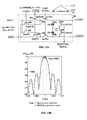
- With reference to
FIG 1A , a first embodiment of a charge sampling (CS)circuit 1 according to the invention is shown. It comprisessampling switch 2, anintegrator 3 and acontrol signal generator 4. Theswitch 2 has a signal input, a signal output and a control input. An analog signal is applied to the signal input of the switch, which is the signal input of thecharge sampling circuit 1, and a sampling signal is applied to the control input from thecontrol signal generator 4. The swith is on, i.e the signal input is connected to the signal output of the switch, only when the sampling signal is in the sampling phase. Theintegrator 3 has a signal input, a signal output, and a control input. The signal output of theswitch 2 is applied to the signal input of theintegrator 3, and a resetting signal from thecontrol signal generator 4 is applied to the control input of theintegrator 3. The current of the analog input signal to theCS circuit 1 is integrated during sampling phase, and the integrated charge produces a proportional voltage or current sample at the signal output of the CS circuit at the end of the sampling phase. The sample is held until the resetting phase of the resetting signal begins, and the time interval in between is the holding phase. A sequence of samples are produced when the phases are repeated, and the signal output is the signal output of said CS circuit. Thecontrol signal generator 4 has a clock input, which is the clock input of the CS circuit, a sampling signal output connected to the control input of theswitch 2 and a resetting signal output connected to the control input of theintergrator 3 as mentioned above. - The
integrator 3 comprises a capacitor 3-1, a resetting switch 3-2 and an optional resistor 3-3 in this embodiment. Theintegrator 3 can, however, have a different configuration in other embodiments. An analog signal is applied to the input of thesampling switch 2. As described, the charge sampling process involves three successive phases: resetting, sampling (t1 to t2) and holding. The time from t1 to t2 is defined as the sampling window.FIG. 1B shows its working waveforms. During the resetting phase, only the resetting switch 3-2 is turned on and the capacitor 3-1 is reset. During the sampling phase, only thesampling switch 2 is turned on, and the signal current is integrated onto the capacitor 3-1. The time constant is large enough to be able to obtain a linear charging when the signal comes from a voltage source (the usual case). If the on-resistance of theswitch 2 is too small, the optional resistor 3-3 can be added. During the holding phase, both switches are in off-state, and the output voltage of theintegrator 3 is held for further use. A pair of interconnected CS circuits, forming a differential CS circuit, provide differential outputs to cancel common mode effects, using a differential input signal and sharing thecontrol signal generator 4. The CS circuits or circuit pairs are used in parallel to increase the sampling rate and to make the time interval between two sampling points possibly less than the sampling window, by time-interleaving both sampling and resetting signals. The signal current can be represented as I(t) =ΣIisin(ωit+φi), i=1, 2, ..., m. The total integrated charge is Q=ΣQi where Qi= (Ii/ωi) (cos (ωit1+φi) -cos (ωit2+φi)) . If ts is the center time of the sampling window, and 2Δt=(t2-t1) is the window width, Qi=(2sin(ωiΔt/ωi)Iisin(ωits+φi)= 2Δt (sin (ωiΔt) / (ωiΔt)) Iisin(ωits,+φi). - Compared with the instant value of the ith component at ts, Ii (ts)=Iisin (ωits+φi), the difference is ki=2Δt(sin(ωiΔt/ωiΔt)), a sampling coefficient depending on frequency ωi and Δt. With this coefficient, the ith frequency component has been precisely sampled at time ts. Since all frequency components are sampled at ts, the total charge on the capacitor naturally represents the signal sample at ts, i.e. ts is the equivalent sampling time point. The frequency response of the CS circuit depends on the function sin(ωiΔt/ωiΔt), shown in
FIG. 1C . Its 3 dB bandwidth equals Δf3dB=1.4/(2πΔt), i.e. 1 GHz for a sampling window of 450 ps, independent of resolution. For voltage sampling, however, the sampling aperture must be smaller than 1 ps for an 8-bit resolution at 1 GHz. Since the function sin(ωiΔt/ωiΔt) is well defined, frequency compensation becomes possible. One way is to let the analog signal pass through a network with a frequency response of (ωiΔt)/sin(ωiΔt) before sampling. Another alternative is to use digital signal processing (DSP) after A/D conversion to compensate the frequency response. - Further, a band pass charge sampling (BPCS) circuit comprises two switches, a weighting-and-sampling (W&S) element, an integrator, and a control signal generator generating a clock, an inverse clock, a W&S signal and a resetting signal. Two ends of a differential signal are applied to the two switch inputs respectively. The two switches, controlled by the clock and the inverse clock respectively, are turned on altemately. Both switch outputs are fed to the W&S element input. The output of W&S element is fed to the integrator input. It works in three successive phases: resetting, sampling and holding. During the resetting phase, the integrator is reset by the resetting signal. Each sampling phase includes n clock cycles, during which the signal current is weighted in the W&S element and integrated in the integrator. During the holding phase, the integrator output is held.
- One embodiment of a band-pass charge sampling (BPCS)
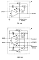
circuit 5 is shown inFIG 2A . It comprises twoswitches element 6, anintegrator 3 and acontrol signal generator 7 generating a clock, an inverse clock, a W&S signal and a resetting signal. Two ends of a differential analog signal are applied to the inputs ofswitches switches switch W&S element 6. The current passing through theW&S element 6 is controlled by the W&S signal. The output ofW&S element 6 is fed to the input ofintegrator 3. Three successive phases are involved for each BPCS process: resetting, sampling and holding.FIG. 2B shows the working waveforms. During the resetting phase, the integrator is reset. Each sampling phase includes n clock cycles forming a sampling window. The signal current through W&S element equals zero outside the sampling window and is weighted according to the weighting function (constant, linear, Gauss or other fuctions) within the sampling window. The weighting function depends on the combination of theW&S element 6 and the W&S signal. The three W&S signals shown inFIG. 2B , corresponding to the three weighting functions (constant, linear and Gauss) are specifically used for a W&S element in which the current is linearly controlled by the W&S signal. During the holding phase, the output voltage ofintegrator 3 is held for further use. - A
differential BPCS circuit 8 is shown inFIG 3 . It comprises fourswitches element 9, adifferential integrator 10, and acontrol signal generator 7, as connected. The shown type ofD-W&S element 9 comprises twoparallel W&S elements parallel integrators D-W&S element 9 and thedifferential integrator 10 may be in other types. Thedifferential BPCS circuit 8 works in the same way as the single endedBPCS circuit 5 except to produce two outputs differentially. Thedifferential BPCS circuit 8 effectively cancels the common mode effects and gives more accurate results. -
FIG 4 shows a paralleldifferential BPCS circuit 11. It comprises fourswitches D-W&S elements differential integrators control signal generator 13, as connected. Each pair of the D-W &S element and the differential integrator, 9A+10A, 9B+10B, ..., 9X+10X, together with theswitches differential BPCS circuit 8. The W&S signals and the resetting signals to these pairs, generated by thecontrol signal generator 13, are evenly time-interleaved. TheMUX 12 multiplexes the outputs of thedifferential integrators control signal generator 13. As a whole, the parallel BPCS circuit gives a higher sampling rate and makes the time interval between two successive sampling points possibly less than the sampling window. Ifswitches 2C and 2D are removed, and the differential W&S elements and the differential integrators are replaced by single-ended versions, it becomes a parallel single-ended BPCS circuit. - A filter function of the BPCS circuits is illustrated in
FIG 5 . From top-down, the frequency increases from DC to 3f,c where fc is the clock frequency. Note that during the negative clock phase the same signal is connected oppositely, which is reflected in the diagram by changing the signal sign. The normalized amplitudes of resulting charges, i.e. the sums of the areas, integrated in n clock cycles are listed inFIG 5 respectively. It is obvious that for input signals with frequencies much higher or lower than fc, the charges cancel each other almost completely, resulting in nearly zero output. For input signals with certain frequencies like fc/4, fc/2, 2fc, ..., the charges are completely cancelled no matter what are their phases. For input signals with frequencies near to fc, the charges are only partly cancelled. When fin=fc, the charges are fully added to each other if it is in-phase with fc while fully cancelled when it is in π/2 phase with fc (not shown inFIG. 5 ). There is a bandwidth in which the signal charges can be effectively integrated. Outside the bandwidth, the signal charges are either completely or substantially cancelled. This is obviously a filter function. It means that the noise with frequencies outside the bandwidth will be cancelled as well. - An ideal frequency response of a BPCS circuit is shown in
FIG 6A , which corresponds to a mathematically accurate integration of the signal current in the sampling window. InFIG 6A , n=10 and constant-weighting are assumed, meaning that the weight of the current is kept constant in the 10-clock-cycle sampling window. Further,FIG 6A shows the frequency response from fin= 0 to fin=8fc, where the y-axis is the maximum output amplitude of different frequency components normalized by the maximum output amplitude in the whole frequency range while the x-axis is input frequencies normalized by fc. It can be seen that the same frequency response is repeated after fin>2fc but with lower amplitudes. The output frequency fout equals |fin- (2p-1) fc| for 2 (p-1)fc≤;fin≤2pfc, where p is an integer (≥1). When fin=(2p-1)fc, the output is a DC voltage, and its amplitude depends on the phase relation of fin and fc. For a given p, the same output frequency is obtained for input frequencies finl (<(2p-1)fc) and fin2 (> (2P-1) fc) when (2P-1) fc-finl=fin2-(2p-1)fc, but their phases are different.FIG. 6B shows the output sample waveforms at different input frequencies with fc=1000 MHz and both I (solid line) and Q (dots) phases. It shows that the BPCS circuit is a filter, a mixer and a sampler simultaneously. - In
FIG 7A and FIG 7B , the ideal frequency responses of a constant-weighting BPCS circuit with n=50 and n=500 are shown respectively.FIG 7A shows the frequency response with n=50 in the range of 0< fin <2fc and in the fine range of 0.95fc<fin<1.05fc.FIG 7B shows the frequency response with n=500 in the range of 0<fin<2fc and in the fine range of 0.995fc<fin<1.005fc. It can be seen that Δf3dB=0.018fc with n=50 and Δf3dB=0.0018fc with n=500, i.e. the bandwidth is inversely proportional to n. The amplitudes of far-end frequency components are reduced with the increase of n, but the maximum adjacent peaks in both cases remain almost unchanged, around -13 dB. - An ideal frequency responses of a linear-weighting BPCS circuit with n=50 and n=500 are shown in
FIG 8A and FIG 8B , respectively. Linear-weighting means that during the sampling phase the weight of the current is first linearly increase and then linearly decrease, symmetric to the center of the sampling window.FIG 8A shows the frequency response with n=50 in the range of 0<fin<2fc and in the fine range of 0.9fc<fin<1.1fc.FIG 8B shows the frequency response with n=500 in the range of 0<fin<2fc and in the fine range of 0.99fc<fin<1.01fc. It can be seen that Δf3dB=0.025fc with n=50 and Δf3dB=0.0025fc with n=500, slightly increasing compared to the constant-weighting cases. The amplitudes of far-end frequency components are rapidly reduced with the increase of n. The maximum adjacent peaks are reduced to -26 dB and -27 dB respectively, compared to those of the constant-weighting cases. - In
FIG 9A and FIG 9B , the ideal frequency responses of a Gauss-weighting BPCS circuit are shown. Gauss-weighting means that during the sampling phase the weight of the current varies according to the Gauss function exp(-t2/2σ2) for a given σ, symmetric to the center of the sampling window. The ratio Δt/σ, where Δt is half of the sampling window and σ the standard deviation, is a weighting parameter.FIG. 9A shows the frequency responses of n=75 with Δt/σ=3.5 and n=87 with Δt/σ=4 respectively in the range of 0<fin<2fc. The 3 dB bandwidths are both 0.025fc.FIG 9B shows the frequency responses of n=750 with Δt/σ=3.5 and n=870 with Δt/σ=4 respectively in the range of 0.9fc<fin<1.1 fc The 3 dB bandwidths are both 0.0025fc. The amplitudes of far-end frequency components and the adjacent peaks are substantially reduced with the Gauss-weighting. The maximum adjacent peaks are in the range of -61 dB to -78 dB. - An
implementation 14 of the core of thedifferential BPCS circuit 8, using n-MOS transistors, is shown inFIG 10 . The clocked switches are n-MOS transistors MOS transistors MOS transistors chip MOS capacitors implementation 14 works in all CMOS processes. Parameters of a 0.8 µm CMOS process, however, is used in the HSPICE simulations. The following three implementations are based on theimplementation 14 with particular component values and W&S signal parameters. - An implementation 19 with n=10 in constant-weighting at fc=1000 MHz is shown in
FIG 11A . The clocked switches are n-MOS transistors MOS transistors MOS transistors MOS capacitors FIG 11B shows both the theoretical frequency response in solid line and the HSPICE simulated frequency response in dots for fin=900-1100 MHz. The simulated frequency response is closely in accordance with the theoretical frequency response. In both cases, the maximum adjacent peaks are -13 dB and Δf3dB=18 MHz. - In
FIG 12A , animplementation 24 with n=59 in linear-weighting at fc=1000 MHz is shown. The clocked switches are n-MOS transistors MOS transistors MOS transistors MOS capacitors FIG 12B shows the theoretical frequency response in solid line and the HSPICE simulated frequency response in dots for fin=900-1100 MHz. The simulated frequency response is basically in accordance with the theoretical frequency response. Both have Δf3dB=21 MHz. For theimplementation 24, however, the maximum adjacent peak is -30 dB, lower than that of the theoretical response. This is because the conductance of n-MOS transistors - An
implementation 26 with n=599 in linear weighting at fc=1000 MHz is shown inFIG 13A . The clocked switches are n-MOS transistors MOS transistors MOS transistors MOS capacitors FIG 13B shows the theoretical frequency response in solid line and the HSPICE simulated frequency response in dots for fin=990-1010 MHz. The simulated frequency response is basically in accordance with the theoretical frequency response. Both have Δf3dB=2 MHz. For the same reason mentioned above, the maximum adjacent peak of theimplementation 26 is -30 dB, lower than that of the theoretical response. -
FIG 14A and FIG 14B show active integrators for improving output swing and linearity, respectively. A single endedactive integrator 29 is shown inFIG 14A . It comprises a differential-in-single-out amplifier 30, aninverter 35, acapacitor 31, and switches 32, 33 and 34, as connected. An active integrator always keeps the signal input at virtual ground, eliminating the impact of capacitor voltage on the signal current. The bandwidth ofamplifier 30 needs only to cover the signal base-band not the carrier, which makes it feasible. Theinverter 35 produces an inverted resetting signal with a delay, using the resetting signal as the input, to control theswitch 33 while the resetting signal controls theswitches switches switch 33 is turned off. The voltage ofcapacitor 31 is reset to the input offset voltage of theamplifier 30. During the sampling phase, theswitches switch 33 is turned on. Thecapacitor 31 is charged by the signal current. In the same time, the offset voltage of theamplifier 30 is cancelled. A differentialactive integrator 36 is shown inFIG 14B . It comprises a differential-in-differential-out amplifier 37, twocapacitors 31A and 31B, aninverter 35, and switches 32A, 32B, 33A, 33B, 34A and 34B. It works basically in the same way as theintegrator 29 except uses a differential input signal and gives differential outputs. Theintegrator 29 can replace theintegrator 3 inFIG 1A while theintegrator 36 can replace theintegrator 10 inFIG 3 . -
FIG 15 shows a two-step BPCS circuit 38. It comprises afirst BPCS circuit 39, a choppingcircuit 40, anamplifier 41, asecond BPCS circuit 42, and aclock signal generator 43 generating a second clock. Thefirst BPCS circuit 39 and thesecond BPCS circuit 42 can be any type of theBPCS circuits first BPCS circuit 39, two ends of a differential analog signal are applied to its two inputs respectively, and a first clock is applied to its clock input. Signal samples with a first sample rate are produced from thefirst BPCS circuit 39 and fed to thechopping circuit 40. The samples are chopped symmetrically in time, controlled by the second clock. From the choppingcircuit 40, the chopped signal with a new carrier frequency equal to the chopping frequency is fed to theamplifier 41, and the amplified differential signals are fed to two inputs ofsecond BPCS circuit 42 respectively. Controlled by the second clock, thesecond BPCS circuit 42 produces the final sample output with a second sample rate. The two-step BPCS circuit 38 gives flexibility in performance trade-off. BPCS circuits in more steps can be built based on the two-step BPCS circuit 38. - A front-end sampling
radio receiver architecture 44 is shown inFIG 16 . It comprises alow pass filter 45 with fpass<2fc a differential-out low noise amplifier (LNA) 46, twoBPCS circuits phase shifter 48, and alocal oscillator 49. The radio signal from antenna is applied to the input of thelow pass filter 45. The frequency components above 2fc are greatly attenuated. The output of thelow pass filter 45 is fed to theLNA 46 to produce differential outputs with a large enough amplitude. The differential outputs are fed to the inputs ofBPCS circuits local oscillator 49 is fed to theBPCS circuit 47A while the Q-clock signal reproduced by the 90°phase shifter 48 from the I-clock signal is fed to theBPCS circuit 47B. TheBPCS circuits BPCS circuits BPCS circuits radio receiver architecture 44 has filtering, mixing and sampling functions simultaneously at the front-end, which relaxes the performance demands on A/D conversion, avoids analog filters, and highly utilizes the capability of DSP. In principle, any narrow bandwidth, i.e. any high Q value, is possible. The center frequency of the filtering function can be easily programmed. It is indeed a superior radio receiver architecture with a wide application scope. - The sampling capacitors used in the CS and the BPCS circuits are much larger than that used in a voltage sampling circuit, resulting in low noise and low charge and clock feed-through.
- The BPCS circuit is simultaneously a filter, a mixer and a sampler, capable of working at radio frequencies. The center frequency, the bandwidth and the adjacent selectivity can be set by the clock frequency, the number n and the shape of W&S signal, particularly useful for front-end sampling radio receiver and system-on-chip.
- It is to be understood that even though numerous characteristics and features of the present invention have been set forth in the description, together with details of the function of the invention, the disclosure is illustrative only and changes may be made in detail within the scope of the invention defined by the following claims.
Claims (14)
- A charge sampling (CS) circuit (1), comprising a control signal generator (4) for controlling an analog input signal to the charge sampling circuit (1) to be integrated by an integrator (3) during a sampling phase responsive to a sampling signal from the control signal generator (4), wherein the current of the analog input signal is integrated to an integrated charge for producing a proportional voltage or current sample at a signal output at the end of the sampling phase; wherein said sampling phase is from time t1 to time t2, wherein said sample represents the instant value of said analog signal at time ts=(t1+t2)/2 and differs from said instant value with a coefficient comprising a constant part and a frequency dependent part (sin(2πfiΔt))/(2πfiΔt), where fi is the frequency of the ith component of said analog signal and Δt=(t2 - t1)/2, i.e half of the width of said sampling phase; characterized by
a frequency compensating circuit with a frequency response proportional to (2πfiΔt)/(sin(2πfiΔt)), wherein the frequency compensating circuit is either an analog frequency compensating circuit for passing through of an analog signal before sampling or a digital frequency compensating circuit for compensation of the frequency response after A/D conversion. - A charge sampling (CS) circuit (1) according to claim 1, characterised by a sampling switch (2) having a signal input for analog input signals, a signal output connected to a signal input of said integrator (3), and a control input connected to a sampling signal output of said control signal generator (4) for controlling the switch to be on only when said sampling signal from the generator (4) is in a sampling phase.
- A charge sampling (CS) circuit (1) according to claim 1 or 2, characterised in that the control signal generator (4) is adapted to control the integrator (3) to hold the sample until a resetting signal from the generator (4) is applied to a control input of the integrator (3).
- A differential charge sampling (CS) circuit, characterised by a first and second CS circuit according to any of the claims 1-3, wherein all control signal generators of said CS circuits are replaced by a common control signal generator (4), the signal input of said first CS circuit is a first analog input of said differential CS circuit, the signal input of said second CS circuit is a second input of said differential CS circuit for a differential analog signal, the signal output of said first CS circuit and the signal output of said second CS circuit are the first signal output and the second signal output of said differential CS circuit.
- A differential charge sampling (CS) circuit according to claim 4, characterised in that the integrator (3) of said first CS circuit and the integrator (3) of said second CS circuit forming a single differential integrator with two inputs for integrating the differential current of said analog signal and producing differential samples at said first signal output and a second signal output.
- A parallel CS circuit, comprising a number of CS circuits according to any of the preceding claims 1-3, characterised in that all first signal inputs are connected together as a first analog signal input of said parallel CS circuit, all control signal generators of said CS circuits are replaced by a common control signal generator, a multiplexer having said number signal inputs connected to the signal outputs of said CS circuits respectively, control inputs connected to multiplexing signal outputs of said common control signal generator, and a signal output, for multiplexing the outputs of said CS circuits to the output of said parallel CS circuit when the outputs of said CS circuits are in holding phases, wherein said parallel CS circuit increases the sampling rate and makes the time interval between two successive sampling points short, and the parallel CS circuit is in a single ended version.
- A parallel CS circuit, comprising a number of differential CS circuits according to claim 4 or 5, characterised in that all first inputs are connected together as the first signal input of said parallel CS circuit for receiving a first end of a differential analog signal, all second inputs are connected together as the second signal input of said parallel CS circuit for receiving a second end of said differential analog signal, and all control signal generators of said CS circuits are replaced by a common control signal generator, a multiplexer having said number signal input pairs connected to the signal output pairs of said CS circuits respectively, control inputs connected to multiplexing signal outputs of said common control signal generator, and a signal output pair, for multiplexing the output pairs of said CS circuits to the output pair of said parallel CS circuit when the output pairs of said CS circuits are in holding phases, wherein said parallel CS circuit increases the sampling rate and makes the time interval between two successive sampling points short, and the parallel CS circuit is in a differential version.
- A parallel CS circuit according to claim 6 or 7, characterised in that said control signal generator has a clock input, said number of sampling signal outputs, said number of resetting signal outputs and said number of multiplexing signal outputs, for generating said number of sampling signals at the sampling signal outputs connected to the control inputs of the switches of said CS circuits respectively, and for generating said number of resetting signals at said resetting signal outputs connected to the control inputs of the integrators of the CS circuits respectively, and said number of multiplexing signals are generated at the multiplexing signal outputs, and said resetting signals, said sampling signals and said multiplexing signals are evenly timeinterleaved.
- A CS circuit according to any of the claims 1-3, or 6, characterised in that the frequency compensating circuit is an analog frequency compensating circuit having a signal input for receiving an analog signal, and a signal output, with a frequency response proportional to (2πfiΔt)/(sin(2πfiΔt)), wherein the signal output is connected to the signal input of said CS.
- A CS circuit according to any of the claims 4, 5, or 7, characterised in that the frequency compensating circuit is an analog frequency compensating circuit having a signal input pair for receiving an analog signal, and a signal output pair, with a frequency response proportional to (2πfiΔt)/(sin(2πfiΔt)), wherein the signal output pair is connected to the first signal input and the second signal input of said CS circuit.
- A CS circuit according to any of the claims 1-3, or 6, characterised in that the frequency compensating circuit is a digital frequency compensating circuit with a frequency response proportional to (2πfiΔt)/(sin(2πfiΔt)) connected after an A/D converter converting the signal output of said CS circuits to a digital signal.
- A CS circuit according to any of the claims 4-5, or 7, characterised in that the frequency compensating circuit is a digital frequency compensating circuit with a frequency response proportional to (2πfiΔt)/(sin(2πfiΔt)) connected after an A/D converter converting the signal output pair of said CS circuits to a digital signal.
- A method of charge sampling, comprising the steps of:integrating an analog input signal during a sampling phase, wherein the current of the analog input signal is integrated to an integrated charge, andproducing a proportional voltage or current sample of said integrated charge at the end of said sampling phase,wherein if said sampling phase is from time t1 to time t2, said sample represents the instant value of said analog signal at time ts=(t1+t2)/2 and differs from said instant value with a coefficient consisting of a constant part and a frequency dependent part (sin(2πfiΔt))/(2πfiΔt), where fi is the frequency of the ith component of said analog signal and Δt = (t2 - t1)/2, i.e half of the width of said sampling phase; characterized byperforming frequency compensation with a frequency compensating circuit with a frequency response proportional to (2πtfiΔt)/(sin(2πfiΔt)), wherein the frequency compensating circuit is either an analog frequency compensating circuit for passing through of an analog signal before sampling or a digital frequency compensating circuit for compensation of the frequency response after A/D conversion..
- A method according to claim 13, characterised in that said analog input signal is a differential analog signal, and said proportional voltage or current sample of said integrated charge is a differential signal.
Priority Applications (1)
| Application Number | Priority Date | Filing Date | Title |
|---|---|---|---|
| EP10168098A EP2228800A3 (en) | 1999-09-28 | 2000-09-25 | Versatile charge sampling circuits |
Applications Claiming Priority (3)
| Application Number | Priority Date | Filing Date | Title |
|---|---|---|---|
| SE9903532 | 1999-09-28 | ||
| SE9903532A SE9903532D0 (en) | 1999-09-28 | 1999-09-28 | Versatile charge sampling circuits |
| PCT/SE2000/001854 WO2001024192A1 (en) | 1999-09-28 | 2000-09-25 | Versatile charge sampling circuits |
Related Child Applications (1)
| Application Number | Title | Priority Date | Filing Date |
|---|---|---|---|
| EP10168098.1 Division-Into | 2010-07-01 |
Publications (2)
| Publication Number | Publication Date |
|---|---|
| EP1221166A1 EP1221166A1 (en) | 2002-07-10 |
| EP1221166B1 true EP1221166B1 (en) | 2011-04-20 |
Family
ID=20417207
Family Applications (2)
| Application Number | Title | Priority Date | Filing Date |
|---|---|---|---|
| EP10168098A Withdrawn EP2228800A3 (en) | 1999-09-28 | 2000-09-25 | Versatile charge sampling circuits |
| EP00968260A Expired - Lifetime EP1221166B1 (en) | 1999-09-28 | 2000-09-25 | Versatile charge sampling circuits |
Family Applications Before (1)
| Application Number | Title | Priority Date | Filing Date |
|---|---|---|---|
| EP10168098A Withdrawn EP2228800A3 (en) | 1999-09-28 | 2000-09-25 | Versatile charge sampling circuits |
Country Status (9)
| Country | Link |
|---|---|
| US (3) | US7053673B1 (en) |
| EP (2) | EP2228800A3 (en) |
| JP (2) | JP4685310B2 (en) |
| CN (2) | CN1551505A (en) |
| AT (1) | ATE506677T1 (en) |
| AU (1) | AU7820100A (en) |
| DE (1) | DE60045867D1 (en) |
| SE (1) | SE9903532D0 (en) |
| WO (1) | WO2001024192A1 (en) |
Families Citing this family (17)
| Publication number | Priority date | Publication date | Assignee | Title |
|---|---|---|---|---|
| WO2005031755A1 (en) * | 2003-09-29 | 2005-04-07 | Nokia Corporation | Active current mode sampling circuit |
| JP5046622B2 (en) | 2005-12-13 | 2012-10-10 | パナソニック株式会社 | Sampling filter device |
| US7671658B2 (en) | 2006-05-24 | 2010-03-02 | Panasonic Corporation | Mixer having frequency selection function |
| JP5258559B2 (en) * | 2006-06-08 | 2013-08-07 | パナソニック株式会社 | Discrete filter, sampling mixer and radio apparatus |
| JP2008017220A (en) * | 2006-07-06 | 2008-01-24 | Sony Corp | Charged main filter circuit |
| WO2008050630A1 (en) | 2006-10-23 | 2008-05-02 | Panasonic Corporation | Sampling filter device and radio communication device |
| FR2911449B1 (en) * | 2007-01-16 | 2009-02-27 | Commissariat Energie Atomique | SAMPLE FILTER WITH FINITE IMPULSE RESPONSE |
| US8385874B2 (en) | 2007-03-06 | 2013-02-26 | Panasonic Corporation | Discrete time direct sampling circuit and receiver |
| WO2008142486A1 (en) * | 2007-05-18 | 2008-11-27 | Nokia Corporation | Analogue-to-digital converter |
| WO2009090883A1 (en) * | 2008-01-16 | 2009-07-23 | Panasonic Corporation | Sampling filter device |
| EP2483891A2 (en) * | 2009-09-28 | 2012-08-08 | Arctic Silicon Devices As | Input configuration for analog to digital converter |
| FR2954628B1 (en) * | 2009-12-18 | 2012-02-24 | Commissariat Energie Atomique | DEVICE AND METHOD FOR RECEIVING RF SIGNALS BASED ON A HETERODYNE ARCHITECTURE WITH UNDER-SAMPLING COMPLEX IF |
| US9287851B2 (en) | 2011-03-22 | 2016-03-15 | Ess Technology, Inc. | Finite impulse response filter for producing outputs having different phases |
| WO2012129271A1 (en) * | 2011-03-22 | 2012-09-27 | Ess Technology, Inc. | Finite impulse response filter for producing outputs having different phases |
| ITFO20110009A1 (en) * | 2011-08-12 | 2013-02-13 | Marco Bennati | SYSTEM AND METHOD OF REDUCTION OF NOISE IN CHAMPIONSHIP AMPLIFIERS. |
| US20140049291A1 (en) | 2012-08-14 | 2014-02-20 | Luxen Technologies, Inc. | Noise-resistant sampling circuit and image sensor |
| CN107918443B (en) * | 2016-10-11 | 2020-04-24 | 深圳市中兴微电子技术有限公司 | Signal generation method and device |
Family Cites Families (30)
| Publication number | Priority date | Publication date | Assignee | Title |
|---|---|---|---|---|
| IT1186340B (en) * | 1985-10-29 | 1987-11-26 | Sgs Microelettronica Spa | DIFFERENTIAL INTEGRATOR WITH SWITCHED CONDENSER USING A SINGLE INTEGRATION CONDENSER |
| JPS62145927A (en) * | 1985-12-20 | 1987-06-30 | Hitachi Ltd | Data converter |
| IT1227615B (en) * | 1988-12-22 | 1991-04-22 | Sgs Thomson Microelectronics | FILTER COMPLETELY DIFFERENTIAL WITH SWITCHED CAPACITORS USING OPERATIONAL AMPLIFIERS CMOS WITHOUT COMMON MODE FEEDBACK |
| US5128966A (en) * | 1989-02-15 | 1992-07-07 | Samsung Electronics Co., Ltd. | System for demodulating frequency- or phase-modulated signals by quadrature-phase |
| US5162670A (en) * | 1990-01-26 | 1992-11-10 | Kabushiki Kaisha Toshiba | Sample-and-hold circuit device |
| JP3337241B2 (en) * | 1991-07-26 | 2002-10-21 | テキサス インスツルメンツ インコーポレイテツド | Improved multi-channel sensor interface circuit and manufacturing method thereof |
| JPH06236698A (en) * | 1993-02-10 | 1994-08-23 | Tamagawa Seiki Co Ltd | Sample-hold method and circuit of sine wave |
| EP0620442B1 (en) * | 1993-04-08 | 2001-07-25 | Lecroy S.A. | Charge sampling circuit |
| US5414311A (en) | 1993-09-14 | 1995-05-09 | Carnegie Mellon University | Sample and hold circuit and finite impulse response filter constructed therefrom |
| US5392043A (en) * | 1993-10-04 | 1995-02-21 | General Electric Company | Double-rate sampled signal integrator |
| US5617093A (en) * | 1994-09-30 | 1997-04-01 | Imp, Inc. | Switched capacitor analog circuits with low input capacitance |
| JP2708007B2 (en) * | 1995-03-31 | 1998-02-04 | 日本電気株式会社 | Sample and hold circuit |
| JPH0983588A (en) * | 1995-09-18 | 1997-03-28 | Mitsubishi Electric Corp | Demodulator modulation/demodulation system and demodulation method |
| US5617063A (en) * | 1995-12-13 | 1997-04-01 | Pacific Communication Sciences, Inc. | Matched filters for processing related signal components |
| JP3392670B2 (en) * | 1996-11-28 | 2003-03-31 | 株式会社東芝 | Sampling device |
| EP0863606B1 (en) * | 1997-03-05 | 2003-09-24 | Nec Corporation | Direct conversion receiver capable of cancelling DC offset voltages |
| JPH1127569A (en) * | 1997-07-01 | 1999-01-29 | Fuji Film Micro Device Kk | Signal-sampling device |
| US5982315A (en) * | 1997-09-12 | 1999-11-09 | Qualcomm Incorporated | Multi-loop Σ Δ analog to digital converter |
| US6320459B2 (en) * | 1997-11-24 | 2001-11-20 | Mccullough Rob | Notch filter implemented using analog sampling |
| US6243430B1 (en) * | 1998-01-09 | 2001-06-05 | Qualcomm Incorporated | Noise cancellation circuit in a quadrature downconverter |
| JPH11234150A (en) * | 1998-02-09 | 1999-08-27 | Toshiba Corp | Digital demodulator |
| FI120124B (en) * | 1998-05-29 | 2009-06-30 | Nokia Corp | A method and circuit for sampling a signal at a high sampling rate |
| US6181748B1 (en) * | 1998-07-07 | 2001-01-30 | Macronix International Co. | Pulse shaper apparatus and method for ISDN U-interface |
| JP3568102B2 (en) * | 1998-07-24 | 2004-09-22 | 松下電器産業株式会社 | Direct conversion receiver |
| US6157331A (en) * | 1998-10-01 | 2000-12-05 | Tritech Microelectronics, Ltd. | Sigma delta modulator with automatic saturation detection and recovery |
| US6246867B1 (en) * | 1998-11-17 | 2001-06-12 | Telefonaktiebolaget Lm Ericsson (Publ) | Method and apparatus for saving current while performing signal strength measurements in a homodyne receiver |
| US6366622B1 (en) * | 1998-12-18 | 2002-04-02 | Silicon Wave, Inc. | Apparatus and method for wireless communications |
| US6757340B1 (en) * | 1999-02-22 | 2004-06-29 | Telefonaktiebolaget L M Ericsson (Publ) | Radio receiver and method for preloading an average DC-offset into a channel filter |
| US6201835B1 (en) * | 1999-03-05 | 2001-03-13 | Burr-Brown Corporation | Frequency-shaped pseudo-random chopper stabilization circuit and method for delta-sigma modulator |
| US6943618B1 (en) * | 1999-05-13 | 2005-09-13 | Honeywell International Inc. | Compensation mechanism for compensating bias levels of an operation circuit in response to supply voltage changes |
-
1999
- 1999-09-28 SE SE9903532A patent/SE9903532D0/en unknown
-
2000
- 2000-09-25 EP EP10168098A patent/EP2228800A3/en not_active Withdrawn
- 2000-09-25 EP EP00968260A patent/EP1221166B1/en not_active Expired - Lifetime
- 2000-09-25 JP JP2001527292A patent/JP4685310B2/en not_active Expired - Fee Related
- 2000-09-25 CN CNA2004100598399A patent/CN1551505A/en active Pending
- 2000-09-25 AT AT00968260T patent/ATE506677T1/en not_active IP Right Cessation
- 2000-09-25 CN CNB008135592A patent/CN1174431C/en not_active Expired - Fee Related
- 2000-09-25 DE DE60045867T patent/DE60045867D1/en not_active Expired - Lifetime
- 2000-09-25 AU AU78201/00A patent/AU7820100A/en not_active Abandoned
- 2000-09-25 WO PCT/SE2000/001854 patent/WO2001024192A1/en active Application Filing
- 2000-09-28 US US09/672,803 patent/US7053673B1/en not_active Expired - Fee Related
-
2005
- 2005-04-06 US US11/099,460 patent/US8035421B2/en not_active Expired - Fee Related
- 2005-04-06 US US11/099,488 patent/US7023245B2/en not_active Expired - Fee Related
-
2010
- 2010-12-09 JP JP2010274877A patent/JP4875201B2/en not_active Expired - Fee Related
Also Published As
| Publication number | Publication date |
|---|---|
| JP4875201B2 (en) | 2012-02-15 |
| CN1551505A (en) | 2004-12-01 |
| DE60045867D1 (en) | 2011-06-01 |
| US8035421B2 (en) | 2011-10-11 |
| CN1377504A (en) | 2002-10-30 |
| JP2011103666A (en) | 2011-05-26 |
| WO2001024192A1 (en) | 2001-04-05 |
| EP1221166A1 (en) | 2002-07-10 |
| EP2228800A3 (en) | 2010-09-29 |
| AU7820100A (en) | 2001-04-30 |
| US20050168371A1 (en) | 2005-08-04 |
| SE9903532D0 (en) | 1999-09-28 |
| JP2003510933A (en) | 2003-03-18 |
| JP4685310B2 (en) | 2011-05-18 |
| EP2228800A2 (en) | 2010-09-15 |
| US7023245B2 (en) | 2006-04-04 |
| CN1174431C (en) | 2004-11-03 |
| US20050176397A1 (en) | 2005-08-11 |
| ATE506677T1 (en) | 2011-05-15 |
| US7053673B1 (en) | 2006-05-30 |
Similar Documents
| Publication | Publication Date | Title |
|---|---|---|
| US7023245B2 (en) | Versatile charge sampling circuits | |
| Jakonis et al. | A 2.4-GHz RF sampling receiver front-end in 0.18-/spl mu/m CMOS | |
| Yuan | A charge sampling mixer with embedded filter function for wireless applications | |
| FI120124B (en) | A method and circuit for sampling a signal at a high sampling rate | |
| US7079826B2 (en) | Digitally controlled analog RF filtering in subsampling communication receiver architecture | |
| Song | A fourth-order bandpass delta-sigma modulator with reduced numbers of op amps | |
| WO1996002977A1 (en) | Method and apparatus for alias-driven frequency downconversion (mixing) | |
| Lindfors et al. | A 3-v 230-mhz cmos decimation subsampler | |
| Karvonen et al. | A CMOS quadrature charge-domain sampling circuit with 66-dB SFDR up to 100 MHz | |
| US7003276B2 (en) | Subsampling communication receiver architecture with gain control and RSSI generation | |
| Karvonen et al. | A quadrature charge-domain sampler with embedded FIR and IIR filtering functions | |
| EP1668647B1 (en) | Active current mode sampling circuit | |
| JPH10190468A (en) | Delta sigma type a/d converter | |
| Karvonen et al. | A Hilbert sampler/filter and complex bandpass SC filter for I/Q demodulation | |
| Lindfors et al. | A novel technique for noise reduction in CMOS subsamplers | |
| Xu et al. | A CMOS analog FIR filter with low phase distortion | |
| JPS60154399A (en) | Sample and hold circuit | |
| GB2073979A (en) | Digital-to-analog converter deglitching circuit | |
| Yim et al. | A 200-MHz CMOS I/Q downconverter | |
| Lippolis et al. | Overview on band-pass sampling approaches for on-board processing | |
| Patel et al. | The effect of oversampling on aperture jitter in bandpass sampling receivers | |
| Eriksson et al. | A model for predicting sampler RF bandwidth and conversion loss | |
| Fakatselis et al. | Subsampling digital IF receiver implementations | |
| Capodiferro et al. | A direct wireless signals receivers architecture with noise sources modeling | |
| Takahashi et al. | A voice band Hilbert transformer using switched capacitor technology |
Legal Events
| Date | Code | Title | Description |
|---|---|---|---|
| PUAI | Public reference made under article 153(3) epc to a published international application that has entered the european phase |
Free format text: ORIGINAL CODE: 0009012 |
|
| 17P | Request for examination filed |
Effective date: 20020228 |
|
| AK | Designated contracting states |
Kind code of ref document: A1 Designated state(s): AT BE CH CY DE DK ES FI FR GB GR IE IT LI LU MC NL PT SE |
|
| AX | Request for extension of the european patent |
Free format text: AL;LT;LV;MK;RO;SI |
|
| RAP1 | Party data changed (applicant data changed or rights of an application transferred) |
Owner name: TELEFONAKTIEBOLAGET LM ERICSSON (PUBL) |
|
| 17Q | First examination report despatched |
Effective date: 20070816 |
|
| GRAP | Despatch of communication of intention to grant a patent |
Free format text: ORIGINAL CODE: EPIDOSNIGR1 |
|
| GRAS | Grant fee paid |
Free format text: ORIGINAL CODE: EPIDOSNIGR3 |
|
| GRAA | (expected) grant |
Free format text: ORIGINAL CODE: 0009210 |
|
| AK | Designated contracting states |
Kind code of ref document: B1 Designated state(s): AT BE CH CY DE DK ES FI FR GB GR IE IT LI LU MC NL PT SE |
|
| AX | Request for extension of the european patent |
Extension state: AL LT LV MK RO SI |
|
| REG | Reference to a national code |
Ref country code: GB Ref legal event code: FG4D |
|
| REG | Reference to a national code |
Ref country code: CH Ref legal event code: EP |
|
| REG | Reference to a national code |
Ref country code: IE Ref legal event code: FG4D |
|
| REF | Corresponds to: |
Ref document number: 60045867 Country of ref document: DE Date of ref document: 20110601 Kind code of ref document: P |
|
| REG | Reference to a national code |
Ref country code: DE Ref legal event code: R096 Ref document number: 60045867 Country of ref document: DE Effective date: 20110601 |
|
| REG | Reference to a national code |
Ref country code: NL Ref legal event code: T3 |
|
| LTIE | Lt: invalidation of european patent or patent extension |
Effective date: 20110420 |
|
| PG25 | Lapsed in a contracting state [announced via postgrant information from national office to epo] |
Ref country code: PT Free format text: LAPSE BECAUSE OF FAILURE TO SUBMIT A TRANSLATION OF THE DESCRIPTION OR TO PAY THE FEE WITHIN THE PRESCRIBED TIME-LIMIT Effective date: 20110822 Ref country code: SE Free format text: LAPSE BECAUSE OF FAILURE TO SUBMIT A TRANSLATION OF THE DESCRIPTION OR TO PAY THE FEE WITHIN THE PRESCRIBED TIME-LIMIT Effective date: 20110420 |
|
| PG25 | Lapsed in a contracting state [announced via postgrant information from national office to epo] |
Ref country code: FI Free format text: LAPSE BECAUSE OF FAILURE TO SUBMIT A TRANSLATION OF THE DESCRIPTION OR TO PAY THE FEE WITHIN THE PRESCRIBED TIME-LIMIT Effective date: 20110420 Ref country code: BE Free format text: LAPSE BECAUSE OF FAILURE TO SUBMIT A TRANSLATION OF THE DESCRIPTION OR TO PAY THE FEE WITHIN THE PRESCRIBED TIME-LIMIT Effective date: 20110420 Ref country code: CY Free format text: LAPSE BECAUSE OF FAILURE TO SUBMIT A TRANSLATION OF THE DESCRIPTION OR TO PAY THE FEE WITHIN THE PRESCRIBED TIME-LIMIT Effective date: 20110420 Ref country code: ES Free format text: LAPSE BECAUSE OF FAILURE TO SUBMIT A TRANSLATION OF THE DESCRIPTION OR TO PAY THE FEE WITHIN THE PRESCRIBED TIME-LIMIT Effective date: 20110731 Ref country code: AT Free format text: LAPSE BECAUSE OF FAILURE TO SUBMIT A TRANSLATION OF THE DESCRIPTION OR TO PAY THE FEE WITHIN THE PRESCRIBED TIME-LIMIT Effective date: 20110420 Ref country code: GR Free format text: LAPSE BECAUSE OF FAILURE TO SUBMIT A TRANSLATION OF THE DESCRIPTION OR TO PAY THE FEE WITHIN THE PRESCRIBED TIME-LIMIT Effective date: 20110721 |
|
| PLBE | No opposition filed within time limit |
Free format text: ORIGINAL CODE: 0009261 |
|
| STAA | Information on the status of an ep patent application or granted ep patent |
Free format text: STATUS: NO OPPOSITION FILED WITHIN TIME LIMIT |
|
| PG25 | Lapsed in a contracting state [announced via postgrant information from national office to epo] |
Ref country code: DK Free format text: LAPSE BECAUSE OF FAILURE TO SUBMIT A TRANSLATION OF THE DESCRIPTION OR TO PAY THE FEE WITHIN THE PRESCRIBED TIME-LIMIT Effective date: 20110420 |
|
| 26N | No opposition filed |
Effective date: 20120123 |
|
| PG25 | Lapsed in a contracting state [announced via postgrant information from national office to epo] |
Ref country code: MC Free format text: LAPSE BECAUSE OF NON-PAYMENT OF DUE FEES Effective date: 20110930 |
|
| REG | Reference to a national code |
Ref country code: CH Ref legal event code: PL |
|
| REG | Reference to a national code |
Ref country code: DE Ref legal event code: R097 Ref document number: 60045867 Country of ref document: DE Effective date: 20120123 |
|
| PG25 | Lapsed in a contracting state [announced via postgrant information from national office to epo] |
Ref country code: IT Free format text: LAPSE BECAUSE OF FAILURE TO SUBMIT A TRANSLATION OF THE DESCRIPTION OR TO PAY THE FEE WITHIN THE PRESCRIBED TIME-LIMIT Effective date: 20110420 |
|
| REG | Reference to a national code |
Ref country code: IE Ref legal event code: MM4A |
|
| REG | Reference to a national code |
Ref country code: FR Ref legal event code: ST Effective date: 20120531 |
|
| PG25 | Lapsed in a contracting state [announced via postgrant information from national office to epo] |
Ref country code: IE Free format text: LAPSE BECAUSE OF NON-PAYMENT OF DUE FEES Effective date: 20110925 Ref country code: LI Free format text: LAPSE BECAUSE OF NON-PAYMENT OF DUE FEES Effective date: 20110930 Ref country code: CH Free format text: LAPSE BECAUSE OF NON-PAYMENT OF DUE FEES Effective date: 20110930 |
|
| PG25 | Lapsed in a contracting state [announced via postgrant information from national office to epo] |
Ref country code: FR Free format text: LAPSE BECAUSE OF NON-PAYMENT OF DUE FEES Effective date: 20110930 |
|
| PG25 | Lapsed in a contracting state [announced via postgrant information from national office to epo] |
Ref country code: LU Free format text: LAPSE BECAUSE OF NON-PAYMENT OF DUE FEES Effective date: 20110925 |
|
| REG | Reference to a national code |
Ref country code: DE Ref legal event code: R081 Ref document number: 60045867 Country of ref document: DE Owner name: OPTIS WIRELESS TECHNOLOGY, LLC, PLANO, US Free format text: FORMER OWNER: TELEFONAKTIEBOLAGET LM ERICSSON (PUBL), STOCKHOLM, SE Effective date: 20140618 Ref country code: DE Ref legal event code: R082 Ref document number: 60045867 Country of ref document: DE Representative=s name: HOFFMANN - EITLE, DE Effective date: 20140618 Ref country code: DE Ref legal event code: R082 Ref document number: 60045867 Country of ref document: DE Representative=s name: HOFFMANN - EITLE, DE Effective date: 20120419 Ref country code: DE Ref legal event code: R082 Ref document number: 60045867 Country of ref document: DE Representative=s name: GRUENECKER, KINKELDEY, STOCKMAIR & SCHWANHAEUS, DE Effective date: 20140618 Ref country code: DE Ref legal event code: R082 Ref document number: 60045867 Country of ref document: DE Representative=s name: GRUENECKER, KINKELDEY, STOCKMAIR & SCHWANHAEUS, DE Effective date: 20120419 Ref country code: DE Ref legal event code: R082 Ref document number: 60045867 Country of ref document: DE Representative=s name: GRUENECKER PATENT- UND RECHTSANWAELTE PARTG MB, DE Effective date: 20120419 Ref country code: DE Ref legal event code: R082 Ref document number: 60045867 Country of ref document: DE Representative=s name: GRUENECKER PATENT- UND RECHTSANWAELTE PARTG MB, DE Effective date: 20140618 |
|
| REG | Reference to a national code |
Ref country code: DE Ref legal event code: R082 Ref document number: 60045867 Country of ref document: DE Representative=s name: GRUENECKER, KINKELDEY, STOCKMAIR & SCHWANHAEUS, DE Ref country code: DE Ref legal event code: R082 Ref document number: 60045867 Country of ref document: DE Representative=s name: GRUENECKER PATENT- UND RECHTSANWAELTE PARTG MB, DE |
|
| REG | Reference to a national code |
Ref country code: GB Ref legal event code: 732E Free format text: REGISTERED BETWEEN 20150528 AND 20150603 |
|
| REG | Reference to a national code |
Ref country code: NL Ref legal event code: SD Effective date: 20150629 |
|
| PGFP | Annual fee paid to national office [announced via postgrant information from national office to epo] |
Ref country code: NL Payment date: 20160824 Year of fee payment: 17 |
|
| PGFP | Annual fee paid to national office [announced via postgrant information from national office to epo] |
Ref country code: DE Payment date: 20160823 Year of fee payment: 17 Ref country code: GB Payment date: 20160825 Year of fee payment: 17 |
|
| REG | Reference to a national code |
Ref country code: DE Ref legal event code: R119 Ref document number: 60045867 Country of ref document: DE |
|
| REG | Reference to a national code |
Ref country code: NL Ref legal event code: MM Effective date: 20171001 |
|
| GBPC | Gb: european patent ceased through non-payment of renewal fee |
Effective date: 20170925 |
|
| PG25 | Lapsed in a contracting state [announced via postgrant information from national office to epo] |
Ref country code: NL Free format text: LAPSE BECAUSE OF NON-PAYMENT OF DUE FEES Effective date: 20171001 |
|
| PG25 | Lapsed in a contracting state [announced via postgrant information from national office to epo] |
Ref country code: DE Free format text: LAPSE BECAUSE OF NON-PAYMENT OF DUE FEES Effective date: 20180404 Ref country code: GB Free format text: LAPSE BECAUSE OF NON-PAYMENT OF DUE FEES Effective date: 20170925 |