CN1334603A - Planar plastic packaged module of integrated circuit - Google Patents
Planar plastic packaged module of integrated circuit Download PDFInfo
- Publication number
- CN1334603A CN1334603A CN01122637A CN01122637A CN1334603A CN 1334603 A CN1334603 A CN 1334603A CN 01122637 A CN01122637 A CN 01122637A CN 01122637 A CN01122637 A CN 01122637A CN 1334603 A CN1334603 A CN 1334603A
- Authority
- CN
- China
- Prior art keywords
- lead
- wire
- tce
- chip package
- lead frame
- Prior art date
- Legal status (The legal status is an assumption and is not a legal conclusion. Google has not performed a legal analysis and makes no representation as to the accuracy of the status listed.)
- Granted
Links
Images


Classifications
-
- H—ELECTRICITY
- H01—ELECTRIC ELEMENTS
- H01L—SEMICONDUCTOR DEVICES NOT COVERED BY CLASS H10
- H01L23/00—Details of semiconductor or other solid state devices
- H01L23/16—Fillings or auxiliary members in containers or encapsulations, e.g. centering rings
-
- H—ELECTRICITY
- H01—ELECTRIC ELEMENTS
- H01L—SEMICONDUCTOR DEVICES NOT COVERED BY CLASS H10
- H01L23/00—Details of semiconductor or other solid state devices
- H01L23/48—Arrangements for conducting electric current to or from the solid state body in operation, e.g. leads, terminal arrangements ; Selection of materials therefor
- H01L23/488—Arrangements for conducting electric current to or from the solid state body in operation, e.g. leads, terminal arrangements ; Selection of materials therefor consisting of soldered or bonded constructions
- H01L23/495—Lead-frames or other flat leads
- H01L23/49503—Lead-frames or other flat leads characterised by the die pad
- H01L23/4951—Chip-on-leads or leads-on-chip techniques, i.e. inner lead fingers being used as die pad
-
- H—ELECTRICITY
- H01—ELECTRIC ELEMENTS
- H01L—SEMICONDUCTOR DEVICES NOT COVERED BY CLASS H10
- H01L23/00—Details of semiconductor or other solid state devices
- H01L23/48—Arrangements for conducting electric current to or from the solid state body in operation, e.g. leads, terminal arrangements ; Selection of materials therefor
- H01L23/488—Arrangements for conducting electric current to or from the solid state body in operation, e.g. leads, terminal arrangements ; Selection of materials therefor consisting of soldered or bonded constructions
- H01L23/495—Lead-frames or other flat leads
- H01L23/49541—Geometry of the lead-frame
- H01L23/49548—Cross section geometry
- H01L23/49551—Cross section geometry characterised by bent parts
-
- H—ELECTRICITY
- H01—ELECTRIC ELEMENTS
- H01L—SEMICONDUCTOR DEVICES NOT COVERED BY CLASS H10
- H01L2224/00—Indexing scheme for arrangements for connecting or disconnecting semiconductor or solid-state bodies and methods related thereto as covered by H01L24/00
- H01L2224/01—Means for bonding being attached to, or being formed on, the surface to be connected, e.g. chip-to-package, die-attach, "first-level" interconnects; Manufacturing methods related thereto
- H01L2224/02—Bonding areas; Manufacturing methods related thereto
- H01L2224/04—Structure, shape, material or disposition of the bonding areas prior to the connecting process
- H01L2224/05—Structure, shape, material or disposition of the bonding areas prior to the connecting process of an individual bonding area
- H01L2224/0554—External layer
- H01L2224/05599—Material
-
- H—ELECTRICITY
- H01—ELECTRIC ELEMENTS
- H01L—SEMICONDUCTOR DEVICES NOT COVERED BY CLASS H10
- H01L2224/00—Indexing scheme for arrangements for connecting or disconnecting semiconductor or solid-state bodies and methods related thereto as covered by H01L24/00
- H01L2224/01—Means for bonding being attached to, or being formed on, the surface to be connected, e.g. chip-to-package, die-attach, "first-level" interconnects; Manufacturing methods related thereto
- H01L2224/42—Wire connectors; Manufacturing methods related thereto
- H01L2224/44—Structure, shape, material or disposition of the wire connectors prior to the connecting process
- H01L2224/45—Structure, shape, material or disposition of the wire connectors prior to the connecting process of an individual wire connector
- H01L2224/45001—Core members of the connector
- H01L2224/4501—Shape
- H01L2224/45012—Cross-sectional shape
- H01L2224/45015—Cross-sectional shape being circular
-
- H—ELECTRICITY
- H01—ELECTRIC ELEMENTS
- H01L—SEMICONDUCTOR DEVICES NOT COVERED BY CLASS H10
- H01L2224/00—Indexing scheme for arrangements for connecting or disconnecting semiconductor or solid-state bodies and methods related thereto as covered by H01L24/00
- H01L2224/01—Means for bonding being attached to, or being formed on, the surface to be connected, e.g. chip-to-package, die-attach, "first-level" interconnects; Manufacturing methods related thereto
- H01L2224/42—Wire connectors; Manufacturing methods related thereto
- H01L2224/47—Structure, shape, material or disposition of the wire connectors after the connecting process
- H01L2224/48—Structure, shape, material or disposition of the wire connectors after the connecting process of an individual wire connector
- H01L2224/4805—Shape
- H01L2224/4809—Loop shape
- H01L2224/48091—Arched
-
- H—ELECTRICITY
- H01—ELECTRIC ELEMENTS
- H01L—SEMICONDUCTOR DEVICES NOT COVERED BY CLASS H10
- H01L2224/00—Indexing scheme for arrangements for connecting or disconnecting semiconductor or solid-state bodies and methods related thereto as covered by H01L24/00
- H01L2224/01—Means for bonding being attached to, or being formed on, the surface to be connected, e.g. chip-to-package, die-attach, "first-level" interconnects; Manufacturing methods related thereto
- H01L2224/42—Wire connectors; Manufacturing methods related thereto
- H01L2224/47—Structure, shape, material or disposition of the wire connectors after the connecting process
- H01L2224/48—Structure, shape, material or disposition of the wire connectors after the connecting process of an individual wire connector
- H01L2224/481—Disposition
- H01L2224/48151—Connecting between a semiconductor or solid-state body and an item not being a semiconductor or solid-state body, e.g. chip-to-substrate, chip-to-passive
- H01L2224/48221—Connecting between a semiconductor or solid-state body and an item not being a semiconductor or solid-state body, e.g. chip-to-substrate, chip-to-passive the body and the item being stacked
- H01L2224/48245—Connecting between a semiconductor or solid-state body and an item not being a semiconductor or solid-state body, e.g. chip-to-substrate, chip-to-passive the body and the item being stacked the item being metallic
- H01L2224/48247—Connecting between a semiconductor or solid-state body and an item not being a semiconductor or solid-state body, e.g. chip-to-substrate, chip-to-passive the body and the item being stacked the item being metallic connecting the wire to a bond pad of the item
-
- H—ELECTRICITY
- H01—ELECTRIC ELEMENTS
- H01L—SEMICONDUCTOR DEVICES NOT COVERED BY CLASS H10
- H01L2224/00—Indexing scheme for arrangements for connecting or disconnecting semiconductor or solid-state bodies and methods related thereto as covered by H01L24/00
- H01L2224/01—Means for bonding being attached to, or being formed on, the surface to be connected, e.g. chip-to-package, die-attach, "first-level" interconnects; Manufacturing methods related thereto
- H01L2224/42—Wire connectors; Manufacturing methods related thereto
- H01L2224/47—Structure, shape, material or disposition of the wire connectors after the connecting process
- H01L2224/48—Structure, shape, material or disposition of the wire connectors after the connecting process of an individual wire connector
- H01L2224/481—Disposition
- H01L2224/48151—Connecting between a semiconductor or solid-state body and an item not being a semiconductor or solid-state body, e.g. chip-to-substrate, chip-to-passive
- H01L2224/48221—Connecting between a semiconductor or solid-state body and an item not being a semiconductor or solid-state body, e.g. chip-to-substrate, chip-to-passive the body and the item being stacked
- H01L2224/48245—Connecting between a semiconductor or solid-state body and an item not being a semiconductor or solid-state body, e.g. chip-to-substrate, chip-to-passive the body and the item being stacked the item being metallic
- H01L2224/4826—Connecting between the body and an opposite side of the item with respect to the body
-
- H—ELECTRICITY
- H01—ELECTRIC ELEMENTS
- H01L—SEMICONDUCTOR DEVICES NOT COVERED BY CLASS H10
- H01L2224/00—Indexing scheme for arrangements for connecting or disconnecting semiconductor or solid-state bodies and methods related thereto as covered by H01L24/00
- H01L2224/01—Means for bonding being attached to, or being formed on, the surface to be connected, e.g. chip-to-package, die-attach, "first-level" interconnects; Manufacturing methods related thereto
- H01L2224/42—Wire connectors; Manufacturing methods related thereto
- H01L2224/47—Structure, shape, material or disposition of the wire connectors after the connecting process
- H01L2224/48—Structure, shape, material or disposition of the wire connectors after the connecting process of an individual wire connector
- H01L2224/484—Connecting portions
- H01L2224/48463—Connecting portions the connecting portion on the bonding area of the semiconductor or solid-state body being a ball bond
- H01L2224/48465—Connecting portions the connecting portion on the bonding area of the semiconductor or solid-state body being a ball bond the other connecting portion not on the bonding area being a wedge bond, i.e. ball-to-wedge, regular stitch
-
- H—ELECTRICITY
- H01—ELECTRIC ELEMENTS
- H01L—SEMICONDUCTOR DEVICES NOT COVERED BY CLASS H10
- H01L2224/00—Indexing scheme for arrangements for connecting or disconnecting semiconductor or solid-state bodies and methods related thereto as covered by H01L24/00
- H01L2224/80—Methods for connecting semiconductor or other solid state bodies using means for bonding being attached to, or being formed on, the surface to be connected
- H01L2224/85—Methods for connecting semiconductor or other solid state bodies using means for bonding being attached to, or being formed on, the surface to be connected using a wire connector
- H01L2224/8538—Bonding interfaces outside the semiconductor or solid-state body
- H01L2224/85399—Material
-
- H—ELECTRICITY
- H01—ELECTRIC ELEMENTS
- H01L—SEMICONDUCTOR DEVICES NOT COVERED BY CLASS H10
- H01L24/00—Arrangements for connecting or disconnecting semiconductor or solid-state bodies; Methods or apparatus related thereto
- H01L24/01—Means for bonding being attached to, or being formed on, the surface to be connected, e.g. chip-to-package, die-attach, "first-level" interconnects; Manufacturing methods related thereto
- H01L24/42—Wire connectors; Manufacturing methods related thereto
- H01L24/47—Structure, shape, material or disposition of the wire connectors after the connecting process
- H01L24/48—Structure, shape, material or disposition of the wire connectors after the connecting process of an individual wire connector
-
- H—ELECTRICITY
- H01—ELECTRIC ELEMENTS
- H01L—SEMICONDUCTOR DEVICES NOT COVERED BY CLASS H10
- H01L2924/00—Indexing scheme for arrangements or methods for connecting or disconnecting semiconductor or solid-state bodies as covered by H01L24/00
- H01L2924/0001—Technical content checked by a classifier
- H01L2924/00014—Technical content checked by a classifier the subject-matter covered by the group, the symbol of which is combined with the symbol of this group, being disclosed without further technical details
-
- H—ELECTRICITY
- H01—ELECTRIC ELEMENTS
- H01L—SEMICONDUCTOR DEVICES NOT COVERED BY CLASS H10
- H01L2924/00—Indexing scheme for arrangements or methods for connecting or disconnecting semiconductor or solid-state bodies as covered by H01L24/00
- H01L2924/01—Chemical elements
- H01L2924/01029—Copper [Cu]
-
- H—ELECTRICITY
- H01—ELECTRIC ELEMENTS
- H01L—SEMICONDUCTOR DEVICES NOT COVERED BY CLASS H10
- H01L2924/00—Indexing scheme for arrangements or methods for connecting or disconnecting semiconductor or solid-state bodies as covered by H01L24/00
- H01L2924/10—Details of semiconductor or other solid state devices to be connected
- H01L2924/102—Material of the semiconductor or solid state bodies
- H01L2924/1025—Semiconducting materials
- H01L2924/10251—Elemental semiconductors, i.e. Group IV
- H01L2924/10253—Silicon [Si]
-
- H—ELECTRICITY
- H01—ELECTRIC ELEMENTS
- H01L—SEMICONDUCTOR DEVICES NOT COVERED BY CLASS H10
- H01L2924/00—Indexing scheme for arrangements or methods for connecting or disconnecting semiconductor or solid-state bodies as covered by H01L24/00
- H01L2924/10—Details of semiconductor or other solid state devices to be connected
- H01L2924/11—Device type
- H01L2924/14—Integrated circuits
Abstract
A semiconductor module includes a semiconductor chip, a lead frame having lead fingers, and a down set member within an encapsulant for reduce warpage and providing a more planar package by balancing thermal stress between the lead fingers and the encapsulant. The down set member can be a bent portion of the lead frame. It can also be a separate body, such as a dummy semiconductor chip.
Description
Present invention generally relates to the plastic package of integrated circuit.Relate to more precisely that to be used for reducing plastic packaged module crooked and the improvement structure of more smooth module is provided.The improvement of the module that more exactly relates to provide more smooth lead frame.
Usually, integrated circuit (IC) chip is electrically connected to the outside by the lead frame of highly conductive.The wire bonds solder joint of chip is that the wire of 1mil is connected to thicker and more tough and tensile lead frame conductor by the diameter of jewelry, expensive clothing and other valuables.The wire of chip, jewelry, expensive clothing and other valuables and the adjacent part of lead frame are encapsulated in the moulded plastic; injury-free with protection chip and wire; simultaneously, the lead frame conductor part that extends plastics can be used for being welded to following one deck of the Equipment Part such as printed circuit board (PCB).There is every year thousands of such module selling.
A lot of problems are considered to be related with this encapsulation notion.One of them is exactly crooked.Make the high stress of finished product module bending that integrated circuit (IC) chip is broken and make it cisco unity malfunction.In encapsulation process, or after chip package has been installed in the electronic device that the client uses, can occur crooked and break.The decline of rate of finished products has obviously increased the cost of packaged chip, and the inefficacy that occurs in using can make the client angry.
Even chip does not break, the bending of packaging part also can cause serious problem to the module lead frame attachment in the welding process of printed circuit board.If the plastic packaged module bending, the plane just may be shifted out in the position of lead ends, and some lead ends may not touch the solder joint on the plate in welding step.For fear of this problem, a kind of industrial complanation standard MS-024 that is set up by JEDEC stipulates that all lead-in wires must be smooth, can not exist two lead-in wires that depart from each other above 4mil.
If packaging part is made up of the different materials with different heat expansion coefficient (TCE), will produce the packaging part bending.Silicon, die-attach area and plastic encapsulation agent have very different TCE usually, and in manufacture process or in the use, packaging part will experience the significant change of temperature.So, need a kind of better solution of Plastic Package, avoid causing crooked temperature stress, following the invention provides this solution.
Therefore, an object of the present invention is to provide a kind of method that reduces or eliminates the plastic package bending.
Another object of the present invention provides a kind of crooked leadframe design that reduces.
Another object of the present invention provides each power of a kind of balance, so that avoid crooked lead frame when temperature change.
A feature of the present invention is, lead frame has the element that is used for being electrically connected to chip on a layer, and has on the second layer in the plastic encapsulation agent and be used for the extra element of equilibrium stress.
Advantage of the present invention is that when packaging part stood the big change of temperature, stress was balanced and has avoided bending.
These and other objects of the present invention, characteristics and advantage, have the contact semiconductor chip of solder joint and the chip package of lead frame is implemented by means of comprising, this lead frame has and contact solder joint and separate at least the first distance and be positioned at the lead-in wire finger that is close on the ground floor that contacts solder joint.Encapsulation agent is sealed chip and part lead frame.Be arranged in material on the second layer also at encapsulation agent.This material has the area that comprises length and width on this second layer.This material also has thickness, than thickness big length and width.This material extends second distance from chip, and wherein said second distance is greater than first distance.Material on the second layer is used to provide more smooth packaging part by means of the thermal stress between balance lead frame and the encapsulation agent.
The inventor recognizes that when chip had the area that is significantly less than packaging part, buckling problem was more serious usually.Therefore, along with generations of chip with littler size production, and packaging part is when still keeping identical size, buckling problem just increases.The invention provides a kind ofly provides littler chip and does not increase crooked method in packaging part.In a preferred embodiment of the invention, material is an integral part of lead frame.This be with that part of different layers that are electrically connected to chip on encapsulation agent in the sweep of lead frame.When encapsulation was finished, this material can comprise that part of lead frame that is not electrically connected to lead-in wire.In the another one embodiment, this material is the object that is electrically connected to the bonding welding point of chip such as the wire of no use of second semiconductor chip.Second semiconductor chip can be installed to the band that is used for keeping its position in assembling process.
From following detailed description of the present invention described in the accompanying drawing, above-mentioned purpose, characteristics and advantage with other of the present invention will be apparent, wherein:
Fig. 1 a. is the 3-D view that comprises a semiconductor chip and a module of the lead frame with the underlying part of separating with the lead-in wire finger;
Fig. 1 b. is the 3-D view of the lead frame of Fig. 1 a, shows the underlying part that is connected to lead frame finger link;
Fig. 2 is the 3-D view of another embodiment, shows a module that comprises semiconductor chip and have the lead frame of band underlying part;
Fig. 3 is the 3-D view of another embodiment, shows a module that comprises semiconductor chip and have the lead frame of the underlying part that is connected to the lead-in wire finger;
Fig. 4 a is the 3-D view of another embodiment, shows a module that comprises semiconductor chip, lead frame and analog chip, and this analog chip is positioned at following one deck of lead-in wire finger;
Fig. 4 b is the vertical view of two embodiments, and that of the left side shows and comprise the module that is fixed on the object of one deck under Fig. 4 a analog chip by support, and that of the right shows thickness similar in appearance to chip and be fixed to the object of lead frame connecting rod with band;
Fig. 4 c is the profile of Fig. 4 b embodiment;
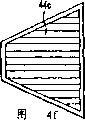
Fig. 4 d-4f is the vertical view with object of different shape; And
Fig. 4 g-4i is the corresponding profile of Fig. 4 d-4f embodiment.
The inventor recognizes, by each power in the balance plastic package, can reduce or avoid crooked.They recognize, when the thickness below the thickness of the plastics above the lead frame is different from lead frame, packaging part just looks like to be bimetal strip, and according to temperature and bending.In order to reduce or to avoid crooked, the inventor provides extra material layer in the plastics at the layer place that is different from lead frame connection lead-in wire, so that each power of balance.In one embodiment, the part of lead frame material is bent to the layer that is different from as the lead frame remainder, so that each power of balance.In another embodiment, the lead-in wire finger is bent downwardly again replys upwards, so that each power better on the balance lead-in wire finger.
As shown in Figure 1a, the curved some 24a of the underlying connecting rod 20 of lead frame 22 in plastic encapsulation agent 26 puts the layer 28 that the 24b place is bent to lead-in wire finger 32 aspects 30 that are starkly lower than lead frame 22 with bending.Layer 28 is selected to provide two material bending power, and this power makes the lead-in wire finger 32 of module 36 and some or all the power on the integrated circuit (IC) chip 34 obtain balance.In addition, underlying connecting rod 20 extends to the position at adjacent chips 34 edges from the position of contiguous packaging part one end, so that make the area maximum of underlying connecting rod 20, and makes underlying effect maximum.So the bending of packaging part is reduced or eliminates.Underlying connecting rod 20 preferably has the A glyph shape, so that provide maximum area in the space that lead-in wire finger 32 is provided, and provides mechanical strength and hardness.By providing several support bars 20 ', also increased stability in underlying connecting rod 20 inside.Support bar 20 ' is oriented the flow direction that is parallel to liquid plastics compound in the patternmaking process, makes when the liquid plastics compound is filled object, and connecting rod is not lifted.The maximum area as far as possible of underlying connecting rod 20 is provided, offsets the power of higher lead-in wire finger 32 with regard to maximum power is provided.Underlying connecting rod 20 is preferably parallel with lead-in wire finger 32, but on different planes.Curved some 24a, 24b clamp the lead frame 22 of contiguous connecting rod 20 by tool using, when finishing with bending operation then and underlying connecting rod 20 instrument of enough bendings is provided when being placed in desirable height and being parallel to lead-in wire finger 32, push down connecting rod 20 and realize.It is 32mil to the minimum interval at chip 34 edges of nominal size and placement is 23mil that underlying connecting rod 20 is designed to make the minimum interval of contiguous lead-in wire finger 32, so that avoid electrical short or mechanical engagement in the module 36.These sizes have ± tolerance of 1mil.Underlying connecting rod 20 also can be provided as has downward slope in encapsulation agent 26.
Desirable is that the lead-in wire finger 2 that is connected to the bonding welding point 35 of chip 34 by bonding wire 37 is arranged in encapsulation agent 26 eminences.Stress between the printed circuit board (not shown) that module 36 and it are fixed thereon is reduced to the degree that lead-in wire finger 32 is lifted in the encapsulation agent 26 of module 36.Therefore, high like that when encapsulation agent 26 comes out by means of a lead-in wire finger 32 is provided as with it, just strengthened connection reliability, simultaneously to circuit board, by means of providing underlying connecting rod 20 to come thermal stress in the balance encapsulation agent 26, the high stress that caused of placing in the module 36 have just been reduced.
Finish with plastics seal after, the lead-in wire finger 32 link 38 (Fig. 1 b) be cut off, and the lead-in wire finger 32 bend in order to be installed to the position of printed circuit board.The link 38 ' (Fig. 1 b) that extends the underlying connecting rod 20 of encapsulation agent 26 is cut off by the edge 26 ' along encapsulation agent 26.Now, underlying connecting rod 20 just separates with chip 34 fully with the remainder of lead frame 22.
The bending that the introducing of underlying connecting rod 20 will approach little profile plastic package (TSOP) has reduced to 2mil from 3.5mil, has promptly reduced 42%.The plastic package that this 40mil is thick has used TCE to be about 13 molded encapsulation agent, has TCE and is 3.5 silicon and be about the lead frame that 4 alloy 42 is made by TCE.To be about 5mil thick for lead-in wire finger 32, and be positioned at apart from the about 9mil of encapsulation agent 26 top surfaces and bottom the encapsulation agent place of about 26mil.It is thick that chip 34 is about 12mil, and be positioned at apart from the about 17mil of encapsulation agent 26 top surfaces place.The tape 46a of the thick about 3mil of lead-in wire finger 32 usefulness is installed in (Fig. 4) on the chip 34.Underlying connecting rod 20, is improved so that provide crooked than the 32 low about 15mil places of the lead-in wire finger in the encapsulation agent 26 by underlying.By means of area that increases underlying connecting rod 20 or increase underlying amount, can obtain crooked further improvement.It is 32mil that underlying connecting rod 20 is designed to make the minimum interval of contiguous lead-in wire finger 32, and is 23mil to the minimum interval of chip 34 ends, so that avoid module 36 interior electrical short or mechanical engagement.
As shown in Figure 2, in flexible embodiment, the various piece of lead-in wire finger 32a is provided with downwards along regional 32a '.In this case, lead-in wire finger 32a has curved some 40a and 40b, so that provide underlying zone 32a ' at layer 30 lower layer 28 place than the lead-in wire finger 32a of lead frame 22a.Except or without underlying connecting rod 20, the underlying part 32a ' of lead-in wire finger 32a can be provided.In addition, the extra finger 33 with underlying zone 33 ' may be provided in the common unappropriated space that respectively goes between between the finger 32a.
As shown in Figure 3, in another flexible embodiment, underlying connecting rod 20a can be connected to one or more lead-in wire finger 32b.In this case, curved some 24a ' and 24b ' provide underlying connecting rod 20a at layer 30 lower layer 28 place than the lead-in wire finger 32a of lead frame 22a.Underlying connecting rod 20a connects lead-in wire finger 32b thereon, preferably is electrically connected to ground.As shown in Figure 3, if desired, underlying connecting rod 20a can be rived.
Shown in Fig. 4 a, in another flexible embodiment, be provided at than layer 28 place in the lower encapsulation agent 26 of the layer 30 of lead-in wire finger 32a such as the object 44 of analog semiconductor chip.The power that object 44 provides power to come balance lead-in wire finger 32a to be provided.Object 44 can be placed on the roughly the same layer of integrated circuit (IC) chip 34 on.In this case, object 44 and chip 34 all are installed in and are used on the tape 46a and 46b of in assembling process fixed object 44 and chip 34 positions.As an alternative, shown in Fig. 4 b and Fig. 4 c, object 44 ' can be placed on the position lower than chip 34.In this case, pillar 50 usefulness tapes are connected to lead-in wire finger 32a to object 44.Utilize the height of pillar can control.Pillar 50 can be in aggregates with object 44 ', and can make in cast or punching operation.Except semiconductor, object 44,44 ' can use the metal such as alloy 42, invar, kovar teleoseal or copper-invar-copper to make.Also can make by enough insulators such as pottery or liquid crystal polymer.Shown in Fig. 4 d-4f, object 44,44 ' can have various shape 44a, 44b, 44c.Can design these shapes and control flowing of encapsulation agent in the assembling process,, thereby object 44,44 ' is locked on the position in the encapsulation agent so that divide big flat surfaces.Provide local extension to pass through object 44,44 ' cavity, flat surfaces is broken, thereby strengthened and the contacting of encapsulation agent, and the problem of having avoided moisture to cause.
Though describe and set forth in the accompanying drawings several embodiment of the present invention and correction thereof herein in detail, obviously, can in the process of design down set member, make multiple further correction and do not depart from scope of the present invention.In above-mentioned specification, do not limit the present invention than claims narrowlyer.The example that provides is just in order to set forth rather than exclusiveness.
Claims (38)
1. chip package comprises:
(a) has the semiconductor chip that contacts solder joint;
(b) have and the described lead frame that contacts welded spot pitch at least the first distance and be positioned at the lead-in wire finger on the ground floor that is close to described contact solder joint;
(c) seal the encapsulation agent of described chip and the described lead frame of part; And
(d) material in the described encapsulation agent, described material is positioned on the second layer, and on the described second layer, has an area that comprises length and width, described material also comprises thickness, described length and width are all greater than described thickness, described material extends second distance from described chip, and wherein said second distance is greater than described first distance, and the described material on the described second layer provides more smooth packaging part by the thermal stress between described lead-in wire finger of balance and the described encapsulation agent.
2. the described chip package of claim 1 is characterized in that, wherein said chip has the area that is significantly less than packaging part.
3. the described chip package of claim 1 is characterized in that, its chips has top surface and the described lead-in wire finger that extends on the described top surface, and wherein said ground floor is determined by described top surface.
4. the described chip package of claim 1 is characterized in that, wherein said material is a lead frame material.
5. the described chip package of claim 4 is characterized in that, wherein said material comprises the sweep of described lead frame, and wherein said sweep is in described encapsulation agent.
6. the described chip package of claim 5 is characterized in that, wherein said sweep extends to the position at contiguous described chip edge from the position at the edge of contiguous described encapsulation agent.
7. the described chip package of claim 5 is characterized in that, wherein said sweep has the A word shape.
8. the described chip package of claim 5 is characterized in that, wherein said sweep comprises and is orientated the support bar that is parallel to the flow direction of liquid plastics compound in the casting process.
9. the described chip package of claim 5 is characterized in that, wherein said material comprises encapsulation is not electrically connected to the lead-in wire finger when finishing the described lead frame of part.
10. the described chip package of claim 9 is characterized in that, wherein said material is separated fully with the lead-in wire finger, to avoid the short circuit of lead-in wire finger.
11. the described chip package of claim 4 is characterized in that, wherein said material comprises the part lead-in wire finger that is bent.
12. the described chip package of claim 1 is characterized in that wherein said encapsulation agent has a TCE, described lead frame has the 2nd TCE, described chip has the 3rd TCE, and described material has the 4th TCE, and wherein said the 4th TCE is significantly less than a described TCE.
13. the described chip package of claim 12 is characterized in that, wherein said the 4th TCE described second and described the 3rd TCE between.
14. the described chip package of claim 12 is characterized in that, wherein the 4th TCE approximates described the 2nd TCE.
15. the described chip package of claim 1 is characterized in that, wherein said contact solder joint is connected to described lead-in wire by wire, and wherein said material comprises the object that is electrically connected to described lead-in wire without wire.
16. the described chip package of claim 15 is characterized in that, also comprises tape, wherein said tape connects described object and described lead-in wire finger, is used for fixing in assembling process the position of described object.
17. the described chip package of claim 16 is characterized in that wherein said object also comprises pillar, wherein said pillar is installed to the described tape that is used for fixing described object space in assembling process.
18. the described chip package of claim 1, it is characterized in that, wherein said lead-in wire finger has the zone that is used for being connected to substrate in described encapsulation agent outside, described lead-in wire finger extends the described encapsulation agent on the described ground floor on the described zone that is used for being connected to substrate, and the wherein said second layer is below ground floor.
19. a method of making chip package comprises the following step:
(a) provide semiconductor chip with contact solder joint;
(b) provide and have and the described lead frame that contacts welded spot pitch at least the first distance and be positioned at the lead-in wire on the ground floor of contiguous described contact solder joint;
(c) seal the described lead frame of described chip and part; And
(d) in described encapsulation agent, provide material, described material is positioned on the second layer, and on the described second layer, has an area that comprises length and width, described material also comprises thickness, described length and described width are all greater than described thickness, described material extends second distance from described chip, and wherein said second distance is greater than described first distance, and the described material on the described second layer provides more smooth packaging part by the thermal stress between described lead-in wire of balance and the described encapsulation agent.
20. the described method of claim 19 is characterized in that wherein said chip has the area that is significantly less than packaging part.
21. the described method of claim 19 is characterized in that, its chips has top surface and extends in described lead-in wire on the described top surface, and wherein said ground floor is determined by described top surface.
22. the described method of claim 19 is characterized in that, wherein said material is an integral part of described lead frame.
23. the described method of claim 22 is characterized in that, the wherein said step (b) that provides comprises the step of the described lead frame of sweep with the described material that forms described step (d), and wherein said sweep is in described encapsulation agent.
24. the described method of claim 23, it is characterized in that, wherein comprise the first curved point and second in the step of the described lead frame of described sweep and bend point, described like this partial parallel is in the other parts of described lead frame, and is positioned at the specified distance below the described other parts of described lead frame.
25. the described method of claim 24 is characterized in that, wherein said bending step (b) comprises with instrument clamps described lead frame and pushes down described part so that the step of the described first and second curved points to be provided.
26. the described chip package of claim 23 is characterized in that, wherein said sweep extends to the position at contiguous described chip edge from the position at contiguous described encapsulation agent edge.
27. the described chip package of claim 23 is characterized in that wherein said sweep has the A word shape.
28. the described method of claim 23 is characterized in that, wherein said sweep comprises encapsulation is not electrically connected to the lead-in wire finger when finishing the described lead frame of part.
29. the described method of claim 23 is characterized in that, the described step that provides step (b) to comprise sweep lead-in wire finger.
30. the described chip package of claim 23 is characterized in that wherein said sweep tilts in described encapsulation agent.
31. the described method of claim 19 is characterized in that wherein said encapsulation agent has a TCE, described lead frame has the 2nd TCE, and described chip has the 3rd TCE, and described material has the 4th TCE, and wherein the 4th TCE is significantly less than a described TCE.
32. the described method of claim 31 is characterized in that, wherein said the 4th TCE is between described the 2nd TCE and described the 3rd TCE.
33. the described method of claim 31 is characterized in that, wherein the 4th TCE approximates described the 2nd TCE.
34. the described method of claim 19 is characterized in that, wherein said contact solder joint is connected to described lead-in wire by wire, wherein saidly provides step (d) to comprise the object that is not electrically connected to described lead-in wire by wire is provided.
35. the described chip package of claim 34 is characterized in that also comprising tape, wherein said tape connects described object and described lead-in wire finger, is used for fixing in assembling process the position of described object.
36. the described chip package of claim 35 is characterized in that wherein said object also comprises pillar, wherein said pillar is installed to the described tape that is used for fixing described object space in assembling process.
37. the described method of claim 19, it is characterized in that, wherein said lead-in wire finger has the zone that is used for being connected to substrate in the encapsulation agent outside, described lead-in wire finger extends the described encapsulation agent on the described ground floor on the described zone that is used for being connected to substrate, and the wherein said second layer is below described ground floor.
38. the described method of claim 19 is characterized in that wherein said encapsulation agent has top surface and lower surface, and wherein said lead-in wire finger extends apart from the described top surface encapsulation agent nearer than described lower surface.
Applications Claiming Priority (3)
| Application Number | Priority Date | Filing Date | Title |
|---|---|---|---|
| US09/605,173 US6603195B1 (en) | 2000-06-28 | 2000-06-28 | Planarized plastic package modules for integrated circuits |
| US09/605173 | 2000-06-28 | ||
| US09/605,173 | 2000-06-28 |
Publications (2)
| Publication Number | Publication Date |
|---|---|
| CN1334603A true CN1334603A (en) | 2002-02-06 |
| CN1180478C CN1180478C (en) | 2004-12-15 |
Family
ID=24422553
Family Applications (1)
| Application Number | Title | Priority Date | Filing Date |
|---|---|---|---|
| CNB011226374A Expired - Fee Related CN1180478C (en) | 2000-06-28 | 2001-06-27 | Planar plastic packaged module of integrated circuit |
Country Status (9)
| Country | Link |
|---|---|
| US (1) | US6603195B1 (en) |
| JP (1) | JP2002043494A (en) |
| KR (1) | KR100444242B1 (en) |
| CN (1) | CN1180478C (en) |
| BR (1) | BR0102606A (en) |
| CA (1) | CA2350057A1 (en) |
| HK (1) | HK1042591B (en) |
| MY (1) | MY119889A (en) |
| TW (1) | TWI231026B (en) |
Cited By (5)
| Publication number | Priority date | Publication date | Assignee | Title |
|---|---|---|---|---|
| CN101540307B (en) * | 2008-03-20 | 2010-10-20 | 力成科技股份有限公司 | Semiconductor encapsulation structure with pins on chip |
| CN101483166B (en) * | 2008-01-10 | 2011-09-07 | 力成科技股份有限公司 | Conductive wire rack with downset spoiler connecting structure and semi-conductor encapsulation construction |
| CN103624909A (en) * | 2012-08-24 | 2014-03-12 | 无锡华润安盛科技有限公司 | Clamp and method for reducing bending of plastic-sealed body |
| CN104956782A (en) * | 2013-01-09 | 2015-09-30 | 德克萨斯仪器股份有限公司 | Integrated circuit module |
| CN115274571A (en) * | 2022-09-30 | 2022-11-01 | 东屹半导体科技(江苏)有限公司 | Semiconductor packaging module with tilting component |
Families Citing this family (7)
| Publication number | Priority date | Publication date | Assignee | Title |
|---|---|---|---|---|
| US7323765B2 (en) * | 2004-10-13 | 2008-01-29 | Atmel Corporation | Die attach paddle for mounting integrated circuit die |
| JP4755214B2 (en) * | 2008-02-22 | 2011-08-24 | 力成科技股▲分▼有限公司 | Lead frame and semiconductor device using the same |
| US7812430B2 (en) * | 2008-03-04 | 2010-10-12 | Powertech Technology Inc. | Leadframe and semiconductor package having downset baffle paddles |
| US7750444B2 (en) * | 2008-05-19 | 2010-07-06 | Powertech Technology Inc. | Lead-on-chip semiconductor package and leadframe for the package |
| US9496214B2 (en) | 2013-05-22 | 2016-11-15 | Toyota Motor Engineering & Manufacturing North American, Inc. | Power electronics devices having thermal stress reduction elements |
| US20140374892A1 (en) * | 2013-06-24 | 2014-12-25 | Yit Meng LEE | Lead frame and semiconductor device using same |
| US9917039B2 (en) * | 2016-04-20 | 2018-03-13 | Amkor Technology, Inc. | Method of forming a semiconductor package with conductive interconnect frame and structure |
Family Cites Families (16)
| Publication number | Priority date | Publication date | Assignee | Title |
|---|---|---|---|---|
| US5229329A (en) * | 1991-02-28 | 1993-07-20 | Texas Instruments, Incorporated | Method of manufacturing insulated lead frame for integrated circuits |
| US5585600A (en) * | 1993-09-02 | 1996-12-17 | International Business Machines Corporation | Encapsulated semiconductor chip module and method of forming the same |
| US5686698A (en) | 1994-06-30 | 1997-11-11 | Motorola, Inc. | Package for electrical components having a molded structure with a port extending into the molded structure |
| US5789806A (en) | 1995-08-02 | 1998-08-04 | National Semiconductor Corporation | Leadframe including bendable support arms for downsetting a die attach pad |
| KR0184076B1 (en) * | 1995-11-28 | 1999-03-20 | 김광호 | Three-dimensional stacked package |
| JP3108856B2 (en) | 1995-12-28 | 2000-11-13 | ローム株式会社 | Resin package type semiconductor device and electronic circuit board mounting the same |
| JPH09186286A (en) * | 1996-01-05 | 1997-07-15 | Matsushita Electron Corp | Lead frame and mounting method for semiconductor chip |
| US5872398A (en) * | 1996-01-11 | 1999-02-16 | Micron Technology, Inc. | Reduced stress LOC assembly including cantilevered leads |
| US6277225B1 (en) * | 1996-03-13 | 2001-08-21 | Micron Technology, Inc. | Stress reduction feature for LOC lead frame |
| KR100196285B1 (en) * | 1996-04-18 | 1999-06-15 | 윤종용 | Addition method of lead and chip, of lead on chip package |
| KR0174983B1 (en) * | 1996-05-10 | 1999-02-01 | 김광호 | Semiconductor chip mounting method and leadframe of loc type semiconductor package |
| US5733800A (en) * | 1996-05-21 | 1998-03-31 | Micron Technology, Inc. | Underfill coating for LOC package |
| JPH09312367A (en) | 1996-05-23 | 1997-12-02 | Mitsubishi Electric Corp | High-frequency semiconductor device |
| JPH1070230A (en) * | 1996-08-27 | 1998-03-10 | Hitachi Cable Ltd | Lead frame for loc |
| KR100216991B1 (en) * | 1996-09-11 | 1999-09-01 | 윤종용 | Leadframe having adhesive layer |
| US6522299B2 (en) * | 1999-04-08 | 2003-02-18 | Cypress Semiconductor Corp. | PC card retractable antenna |
-
2000
- 2000-06-28 US US09/605,173 patent/US6603195B1/en not_active Expired - Lifetime
-
2001
- 2001-06-04 KR KR10-2001-0031081A patent/KR100444242B1/en not_active IP Right Cessation
- 2001-06-07 CA CA002350057A patent/CA2350057A1/en not_active Abandoned
- 2001-06-21 MY MYPI20012927A patent/MY119889A/en unknown
- 2001-06-22 TW TW090115294A patent/TWI231026B/en not_active IP Right Cessation
- 2001-06-27 CN CNB011226374A patent/CN1180478C/en not_active Expired - Fee Related
- 2001-06-27 JP JP2001194587A patent/JP2002043494A/en active Pending
- 2001-06-28 BR BR0102606-2A patent/BR0102606A/en not_active IP Right Cessation
-
2002
- 2002-06-03 HK HK02104209.7A patent/HK1042591B/en not_active IP Right Cessation
Cited By (8)
| Publication number | Priority date | Publication date | Assignee | Title |
|---|---|---|---|---|
| CN101483166B (en) * | 2008-01-10 | 2011-09-07 | 力成科技股份有限公司 | Conductive wire rack with downset spoiler connecting structure and semi-conductor encapsulation construction |
| CN101540307B (en) * | 2008-03-20 | 2010-10-20 | 力成科技股份有限公司 | Semiconductor encapsulation structure with pins on chip |
| CN103624909A (en) * | 2012-08-24 | 2014-03-12 | 无锡华润安盛科技有限公司 | Clamp and method for reducing bending of plastic-sealed body |
| CN103624909B (en) * | 2012-08-24 | 2016-09-07 | 无锡华润安盛科技有限公司 | For reducing fixture and the method thereof of plastic-sealed body bending |
| CN104956782A (en) * | 2013-01-09 | 2015-09-30 | 德克萨斯仪器股份有限公司 | Integrated circuit module |
| CN104956782B (en) * | 2013-01-09 | 2018-05-11 | 德克萨斯仪器股份有限公司 | Integrated circuit modules |
| CN115274571A (en) * | 2022-09-30 | 2022-11-01 | 东屹半导体科技(江苏)有限公司 | Semiconductor packaging module with tilting component |
| CN115274571B (en) * | 2022-09-30 | 2022-12-16 | 东屹半导体科技(江苏)有限公司 | Semiconductor packaging module with tilting component |
Also Published As
| Publication number | Publication date |
|---|---|
| CN1180478C (en) | 2004-12-15 |
| BR0102606A (en) | 2002-02-13 |
| HK1042591B (en) | 2005-05-13 |
| CA2350057A1 (en) | 2001-12-28 |
| KR100444242B1 (en) | 2004-08-11 |
| MY119889A (en) | 2005-07-29 |
| KR20020001521A (en) | 2002-01-09 |
| TWI231026B (en) | 2005-04-11 |
| JP2002043494A (en) | 2002-02-08 |
| US6603195B1 (en) | 2003-08-05 |
| HK1042591A1 (en) | 2002-08-16 |
Similar Documents
| Publication | Publication Date | Title |
|---|---|---|
| US10796983B2 (en) | Positional relationship among components of semiconductor device | |
| US5783861A (en) | Semiconductor package and lead frame | |
| US6949816B2 (en) | Semiconductor component having first surface area for electrically coupling to a semiconductor chip and second surface area for electrically coupling to a substrate, and method of manufacturing same | |
| KR960005042B1 (en) | Semiconductor package | |
| CN1180478C (en) | Planar plastic packaged module of integrated circuit | |
| CN1153997A (en) | Improved integrated chip package with reduced dimensions | |
| US7439612B2 (en) | Integrated circuit package structure with gap through lead bar between a die edge and an attachment point corresponding to a conductive connector | |
| US20170047273A1 (en) | Package structure and the method to fabricate thereof | |
| EP0118237B1 (en) | Lead frame for a semiconductor element | |
| WO2006091940A1 (en) | Integrated circuit package with lead stops | |
| US20100314728A1 (en) | Ic package having an inductor etched into a leadframe thereof | |
| KR19980055815A (en) | Ball Grid Array Semiconductor Package | |
| US6921967B2 (en) | Reinforced die pad support structure | |
| US6455922B1 (en) | Deformation-absorbing leadframe for semiconductor devices | |
| EP0443044A1 (en) | Lead frame for semiconductor device and semiconductor device using the lead frame | |
| CN112956005A (en) | Integrated circuit package including inwardly bent leads | |
| US20230260879A1 (en) | Three-dimensional functional integration | |
| JP3211116B2 (en) | Electronic component and its module structure | |
| KR930020648A (en) | Semiconductor lead frame | |
| KR100525452B1 (en) | Semiconductor package & PCB mounted with the same | |
| JP2504901B2 (en) | Method for manufacturing multiple electronic component packages | |
| KR19990039945U (en) | Semiconductor package | |
| KR20000051981A (en) | Lead frame structure for preventing the warping of semiconductor package body | |
| JPS61166054A (en) | Semiconductor device | |
| KR19990085636A (en) | Copper-based lead frame and semiconductor chip package using same |
Legal Events
| Date | Code | Title | Description |
|---|---|---|---|
| C10 | Entry into substantive examination | ||
| SE01 | Entry into force of request for substantive examination | ||
| C06 | Publication | ||
| PB01 | Publication | ||
| C14 | Grant of patent or utility model | ||
| GR01 | Patent grant | ||
| C17 | Cessation of patent right | ||
| CF01 | Termination of patent right due to non-payment of annual fee |
Granted publication date: 20041215 Termination date: 20120627 |