CN1267996C - Semiconductor device and its manufacturing method - Google Patents
Semiconductor device and its manufacturing method Download PDFInfo
- Publication number
- CN1267996C CN1267996C CNB018083439A CN01808343A CN1267996C CN 1267996 C CN1267996 C CN 1267996C CN B018083439 A CNB018083439 A CN B018083439A CN 01808343 A CN01808343 A CN 01808343A CN 1267996 C CN1267996 C CN 1267996C
- Authority
- CN
- China
- Prior art keywords
- mentioned
- storage card
- semiconductor device
- mounting portion
- basal substrate
- Prior art date
- Legal status (The legal status is an assumption and is not a legal conclusion. Google has not performed a legal analysis and makes no representation as to the accuracy of the status listed.)
- Expired - Fee Related
Links
Images


Classifications
-
- G—PHYSICS
- G06—COMPUTING; CALCULATING OR COUNTING
- G06K—GRAPHICAL DATA READING; PRESENTATION OF DATA; RECORD CARRIERS; HANDLING RECORD CARRIERS
- G06K19/00—Record carriers for use with machines and with at least a part designed to carry digital markings
- G06K19/06—Record carriers for use with machines and with at least a part designed to carry digital markings characterised by the kind of the digital marking, e.g. shape, nature, code
- G06K19/067—Record carriers with conductive marks, printed circuits or semiconductor circuit elements, e.g. credit or identity cards also with resonating or responding marks without active components
- G06K19/07—Record carriers with conductive marks, printed circuits or semiconductor circuit elements, e.g. credit or identity cards also with resonating or responding marks without active components with integrated circuit chips
- G06K19/077—Constructional details, e.g. mounting of circuits in the carrier
-
- G—PHYSICS
- G06—COMPUTING; CALCULATING OR COUNTING
- G06K—GRAPHICAL DATA READING; PRESENTATION OF DATA; RECORD CARRIERS; HANDLING RECORD CARRIERS
- G06K19/00—Record carriers for use with machines and with at least a part designed to carry digital markings
- G06K19/06—Record carriers for use with machines and with at least a part designed to carry digital markings characterised by the kind of the digital marking, e.g. shape, nature, code
- G06K19/067—Record carriers with conductive marks, printed circuits or semiconductor circuit elements, e.g. credit or identity cards also with resonating or responding marks without active components
- G06K19/07—Record carriers with conductive marks, printed circuits or semiconductor circuit elements, e.g. credit or identity cards also with resonating or responding marks without active components with integrated circuit chips
- G06K19/077—Constructional details, e.g. mounting of circuits in the carrier
- G06K19/0772—Physical layout of the record carrier
- G06K19/07732—Physical layout of the record carrier the record carrier having a housing or construction similar to well-known portable memory devices, such as SD cards, USB or memory sticks
-
- G—PHYSICS
- G06—COMPUTING; CALCULATING OR COUNTING
- G06K—GRAPHICAL DATA READING; PRESENTATION OF DATA; RECORD CARRIERS; HANDLING RECORD CARRIERS
- G06K19/00—Record carriers for use with machines and with at least a part designed to carry digital markings
- G06K19/06—Record carriers for use with machines and with at least a part designed to carry digital markings characterised by the kind of the digital marking, e.g. shape, nature, code
- G06K19/067—Record carriers with conductive marks, printed circuits or semiconductor circuit elements, e.g. credit or identity cards also with resonating or responding marks without active components
- G06K19/07—Record carriers with conductive marks, printed circuits or semiconductor circuit elements, e.g. credit or identity cards also with resonating or responding marks without active components with integrated circuit chips
- G06K19/077—Constructional details, e.g. mounting of circuits in the carrier
- G06K19/07737—Constructional details, e.g. mounting of circuits in the carrier the record carrier consisting of two or more mechanically separable parts
- G06K19/07739—Constructional details, e.g. mounting of circuits in the carrier the record carrier consisting of two or more mechanically separable parts comprising a first part capable of functioning as a record carrier on its own and a second part being only functional as a form factor changing part, e.g. SIM cards type ID 0001, removably attached to a regular smart card form factor
-
- G—PHYSICS
- G06—COMPUTING; CALCULATING OR COUNTING
- G06K—GRAPHICAL DATA READING; PRESENTATION OF DATA; RECORD CARRIERS; HANDLING RECORD CARRIERS
- G06K19/00—Record carriers for use with machines and with at least a part designed to carry digital markings
- G06K19/06—Record carriers for use with machines and with at least a part designed to carry digital markings characterised by the kind of the digital marking, e.g. shape, nature, code
- G06K19/067—Record carriers with conductive marks, printed circuits or semiconductor circuit elements, e.g. credit or identity cards also with resonating or responding marks without active components
- G06K19/07—Record carriers with conductive marks, printed circuits or semiconductor circuit elements, e.g. credit or identity cards also with resonating or responding marks without active components with integrated circuit chips
- G06K19/077—Constructional details, e.g. mounting of circuits in the carrier
- G06K19/07743—External electrical contacts
-
- G—PHYSICS
- G11—INFORMATION STORAGE
- G11C—STATIC STORES
- G11C5/00—Details of stores covered by group G11C11/00
- G11C5/02—Disposition of storage elements, e.g. in the form of a matrix array
- G11C5/04—Supports for storage elements, e.g. memory modules; Mounting or fixing of storage elements on such supports
-
- H—ELECTRICITY
- H01—ELECTRIC ELEMENTS
- H01L—SEMICONDUCTOR DEVICES NOT COVERED BY CLASS H10
- H01L23/00—Details of semiconductor or other solid state devices
- H01L23/52—Arrangements for conducting electric current within the device in operation from one component to another, i.e. interconnections, e.g. wires, lead frames
- H01L23/538—Arrangements for conducting electric current within the device in operation from one component to another, i.e. interconnections, e.g. wires, lead frames the interconnection structure between a plurality of semiconductor chips being formed on, or in, insulating substrates
- H01L23/5388—Arrangements for conducting electric current within the device in operation from one component to another, i.e. interconnections, e.g. wires, lead frames the interconnection structure between a plurality of semiconductor chips being formed on, or in, insulating substrates for flat cards, e.g. credit cards
-
- H—ELECTRICITY
- H01—ELECTRIC ELEMENTS
- H01L—SEMICONDUCTOR DEVICES NOT COVERED BY CLASS H10
- H01L24/00—Arrangements for connecting or disconnecting semiconductor or solid-state bodies; Methods or apparatus related thereto
- H01L24/93—Batch processes
- H01L24/95—Batch processes at chip-level, i.e. with connecting carried out on a plurality of singulated devices, i.e. on diced chips
- H01L24/97—Batch processes at chip-level, i.e. with connecting carried out on a plurality of singulated devices, i.e. on diced chips the devices being connected to a common substrate, e.g. interposer, said common substrate being separable into individual assemblies after connecting
-
- H—ELECTRICITY
- H01—ELECTRIC ELEMENTS
- H01L—SEMICONDUCTOR DEVICES NOT COVERED BY CLASS H10
- H01L25/00—Assemblies consisting of a plurality of individual semiconductor or other solid state devices ; Multistep manufacturing processes thereof
- H01L25/18—Assemblies consisting of a plurality of individual semiconductor or other solid state devices ; Multistep manufacturing processes thereof the devices being of types provided for in two or more different subgroups of the same main group of groups H01L27/00 - H01L33/00, or in a single subclass of H10K, H10N
-
- H—ELECTRICITY
- H05—ELECTRIC TECHNIQUES NOT OTHERWISE PROVIDED FOR
- H05K—PRINTED CIRCUITS; CASINGS OR CONSTRUCTIONAL DETAILS OF ELECTRIC APPARATUS; MANUFACTURE OF ASSEMBLAGES OF ELECTRICAL COMPONENTS
- H05K5/00—Casings, cabinets or drawers for electric apparatus
- H05K5/02—Details
- H05K5/0256—Details of interchangeable modules or receptacles therefor, e.g. cartridge mechanisms
- H05K5/026—Details of interchangeable modules or receptacles therefor, e.g. cartridge mechanisms having standardized interfaces
-
- H—ELECTRICITY
- H05—ELECTRIC TECHNIQUES NOT OTHERWISE PROVIDED FOR
- H05K—PRINTED CIRCUITS; CASINGS OR CONSTRUCTIONAL DETAILS OF ELECTRIC APPARATUS; MANUFACTURE OF ASSEMBLAGES OF ELECTRICAL COMPONENTS
- H05K5/00—Casings, cabinets or drawers for electric apparatus
- H05K5/02—Details
- H05K5/0256—Details of interchangeable modules or receptacles therefor, e.g. cartridge mechanisms
- H05K5/0282—Adapters for connecting cards having a first standard in receptacles having a second standard
-
- H—ELECTRICITY
- H01—ELECTRIC ELEMENTS
- H01L—SEMICONDUCTOR DEVICES NOT COVERED BY CLASS H10
- H01L2224/00—Indexing scheme for arrangements for connecting or disconnecting semiconductor or solid-state bodies and methods related thereto as covered by H01L24/00
- H01L2224/01—Means for bonding being attached to, or being formed on, the surface to be connected, e.g. chip-to-package, die-attach, "first-level" interconnects; Manufacturing methods related thereto
- H01L2224/02—Bonding areas; Manufacturing methods related thereto
- H01L2224/04—Structure, shape, material or disposition of the bonding areas prior to the connecting process
- H01L2224/05—Structure, shape, material or disposition of the bonding areas prior to the connecting process of an individual bonding area
- H01L2224/0554—External layer
- H01L2224/0555—Shape
- H01L2224/05552—Shape in top view
- H01L2224/05554—Shape in top view being square
-
- H—ELECTRICITY
- H01—ELECTRIC ELEMENTS
- H01L—SEMICONDUCTOR DEVICES NOT COVERED BY CLASS H10
- H01L2224/00—Indexing scheme for arrangements for connecting or disconnecting semiconductor or solid-state bodies and methods related thereto as covered by H01L24/00
- H01L2224/01—Means for bonding being attached to, or being formed on, the surface to be connected, e.g. chip-to-package, die-attach, "first-level" interconnects; Manufacturing methods related thereto
- H01L2224/02—Bonding areas; Manufacturing methods related thereto
- H01L2224/04—Structure, shape, material or disposition of the bonding areas prior to the connecting process
- H01L2224/05—Structure, shape, material or disposition of the bonding areas prior to the connecting process of an individual bonding area
- H01L2224/0554—External layer
- H01L2224/05599—Material
-
- H—ELECTRICITY
- H01—ELECTRIC ELEMENTS
- H01L—SEMICONDUCTOR DEVICES NOT COVERED BY CLASS H10
- H01L2224/00—Indexing scheme for arrangements for connecting or disconnecting semiconductor or solid-state bodies and methods related thereto as covered by H01L24/00
- H01L2224/01—Means for bonding being attached to, or being formed on, the surface to be connected, e.g. chip-to-package, die-attach, "first-level" interconnects; Manufacturing methods related thereto
- H01L2224/42—Wire connectors; Manufacturing methods related thereto
- H01L2224/44—Structure, shape, material or disposition of the wire connectors prior to the connecting process
- H01L2224/45—Structure, shape, material or disposition of the wire connectors prior to the connecting process of an individual wire connector
- H01L2224/45001—Core members of the connector
- H01L2224/45099—Material
- H01L2224/451—Material with a principal constituent of the material being a metal or a metalloid, e.g. boron (B), silicon (Si), germanium (Ge), arsenic (As), antimony (Sb), tellurium (Te) and polonium (Po), and alloys thereof
- H01L2224/45138—Material with a principal constituent of the material being a metal or a metalloid, e.g. boron (B), silicon (Si), germanium (Ge), arsenic (As), antimony (Sb), tellurium (Te) and polonium (Po), and alloys thereof the principal constituent melting at a temperature of greater than or equal to 950°C and less than 1550°C
- H01L2224/45144—Gold (Au) as principal constituent
-
- H—ELECTRICITY
- H01—ELECTRIC ELEMENTS
- H01L—SEMICONDUCTOR DEVICES NOT COVERED BY CLASS H10
- H01L2224/00—Indexing scheme for arrangements for connecting or disconnecting semiconductor or solid-state bodies and methods related thereto as covered by H01L24/00
- H01L2224/01—Means for bonding being attached to, or being formed on, the surface to be connected, e.g. chip-to-package, die-attach, "first-level" interconnects; Manufacturing methods related thereto
- H01L2224/42—Wire connectors; Manufacturing methods related thereto
- H01L2224/47—Structure, shape, material or disposition of the wire connectors after the connecting process
- H01L2224/48—Structure, shape, material or disposition of the wire connectors after the connecting process of an individual wire connector
- H01L2224/481—Disposition
- H01L2224/48151—Connecting between a semiconductor or solid-state body and an item not being a semiconductor or solid-state body, e.g. chip-to-substrate, chip-to-passive
- H01L2224/48221—Connecting between a semiconductor or solid-state body and an item not being a semiconductor or solid-state body, e.g. chip-to-substrate, chip-to-passive the body and the item being stacked
- H01L2224/48225—Connecting between a semiconductor or solid-state body and an item not being a semiconductor or solid-state body, e.g. chip-to-substrate, chip-to-passive the body and the item being stacked the item being non-metallic, e.g. insulating substrate with or without metallisation
- H01L2224/48227—Connecting between a semiconductor or solid-state body and an item not being a semiconductor or solid-state body, e.g. chip-to-substrate, chip-to-passive the body and the item being stacked the item being non-metallic, e.g. insulating substrate with or without metallisation connecting the wire to a bond pad of the item
-
- H—ELECTRICITY
- H01—ELECTRIC ELEMENTS
- H01L—SEMICONDUCTOR DEVICES NOT COVERED BY CLASS H10
- H01L2224/00—Indexing scheme for arrangements for connecting or disconnecting semiconductor or solid-state bodies and methods related thereto as covered by H01L24/00
- H01L2224/80—Methods for connecting semiconductor or other solid state bodies using means for bonding being attached to, or being formed on, the surface to be connected
- H01L2224/85—Methods for connecting semiconductor or other solid state bodies using means for bonding being attached to, or being formed on, the surface to be connected using a wire connector
- H01L2224/8538—Bonding interfaces outside the semiconductor or solid-state body
- H01L2224/85399—Material
-
- H—ELECTRICITY
- H01—ELECTRIC ELEMENTS
- H01L—SEMICONDUCTOR DEVICES NOT COVERED BY CLASS H10
- H01L24/00—Arrangements for connecting or disconnecting semiconductor or solid-state bodies; Methods or apparatus related thereto
- H01L24/01—Means for bonding being attached to, or being formed on, the surface to be connected, e.g. chip-to-package, die-attach, "first-level" interconnects; Manufacturing methods related thereto
- H01L24/42—Wire connectors; Manufacturing methods related thereto
- H01L24/44—Structure, shape, material or disposition of the wire connectors prior to the connecting process
- H01L24/45—Structure, shape, material or disposition of the wire connectors prior to the connecting process of an individual wire connector
-
- H—ELECTRICITY
- H01—ELECTRIC ELEMENTS
- H01L—SEMICONDUCTOR DEVICES NOT COVERED BY CLASS H10
- H01L24/00—Arrangements for connecting or disconnecting semiconductor or solid-state bodies; Methods or apparatus related thereto
- H01L24/01—Means for bonding being attached to, or being formed on, the surface to be connected, e.g. chip-to-package, die-attach, "first-level" interconnects; Manufacturing methods related thereto
- H01L24/42—Wire connectors; Manufacturing methods related thereto
- H01L24/47—Structure, shape, material or disposition of the wire connectors after the connecting process
- H01L24/48—Structure, shape, material or disposition of the wire connectors after the connecting process of an individual wire connector
-
- H—ELECTRICITY
- H01—ELECTRIC ELEMENTS
- H01L—SEMICONDUCTOR DEVICES NOT COVERED BY CLASS H10
- H01L2924/00—Indexing scheme for arrangements or methods for connecting or disconnecting semiconductor or solid-state bodies as covered by H01L24/00
- H01L2924/0001—Technical content checked by a classifier
- H01L2924/00014—Technical content checked by a classifier the subject-matter covered by the group, the symbol of which is combined with the symbol of this group, being disclosed without further technical details
-
- H—ELECTRICITY
- H01—ELECTRIC ELEMENTS
- H01L—SEMICONDUCTOR DEVICES NOT COVERED BY CLASS H10
- H01L2924/00—Indexing scheme for arrangements or methods for connecting or disconnecting semiconductor or solid-state bodies as covered by H01L24/00
- H01L2924/01—Chemical elements
- H01L2924/01039—Yttrium [Y]
-
- H—ELECTRICITY
- H01—ELECTRIC ELEMENTS
- H01L—SEMICONDUCTOR DEVICES NOT COVERED BY CLASS H10
- H01L2924/00—Indexing scheme for arrangements or methods for connecting or disconnecting semiconductor or solid-state bodies as covered by H01L24/00
- H01L2924/01—Chemical elements
- H01L2924/01078—Platinum [Pt]
-
- H—ELECTRICITY
- H01—ELECTRIC ELEMENTS
- H01L—SEMICONDUCTOR DEVICES NOT COVERED BY CLASS H10
- H01L2924/00—Indexing scheme for arrangements or methods for connecting or disconnecting semiconductor or solid-state bodies as covered by H01L24/00
- H01L2924/01—Chemical elements
- H01L2924/01079—Gold [Au]
-
- H—ELECTRICITY
- H01—ELECTRIC ELEMENTS
- H01L—SEMICONDUCTOR DEVICES NOT COVERED BY CLASS H10
- H01L2924/00—Indexing scheme for arrangements or methods for connecting or disconnecting semiconductor or solid-state bodies as covered by H01L24/00
- H01L2924/10—Details of semiconductor or other solid state devices to be connected
- H01L2924/1015—Shape
- H01L2924/1016—Shape being a cuboid
- H01L2924/10161—Shape being a cuboid with a rectangular active surface
-
- H—ELECTRICITY
- H01—ELECTRIC ELEMENTS
- H01L—SEMICONDUCTOR DEVICES NOT COVERED BY CLASS H10
- H01L2924/00—Indexing scheme for arrangements or methods for connecting or disconnecting semiconductor or solid-state bodies as covered by H01L24/00
- H01L2924/10—Details of semiconductor or other solid state devices to be connected
- H01L2924/11—Device type
- H01L2924/14—Integrated circuits
-
- H—ELECTRICITY
- H01—ELECTRIC ELEMENTS
- H01L—SEMICONDUCTOR DEVICES NOT COVERED BY CLASS H10
- H01L2924/00—Indexing scheme for arrangements or methods for connecting or disconnecting semiconductor or solid-state bodies as covered by H01L24/00
- H01L2924/15—Details of package parts other than the semiconductor or other solid state devices to be connected
- H01L2924/181—Encapsulation
Abstract
An adapter fitting portion (3a) having a projection in cross section is provided to a cap (3) of a small-sized memory card (1) and integrally fitted into a recess portion of an adapter (2) in a detachable way. The size compatibility of the memory card (1) with an existing memory card is achieved. The memory card (1) can be used also for an apparatus adapted to an existing memory card.
Description
Technical field
The present invention relates to semiconductor device and manufacturing technology thereof, for example, relate in semiconductor memory card (below, abbreviate storage card as) and using and otherwise effective technique.
Background technology
The storage card of multimedia card (U.S. Sun Disk company) or SD card (Panasonic, Toshiba, Sun Disk) etc. and so on is one of the storage device of the semiconductor memory chips inner storag information of portion within it.If use this storage card, owing to directly and electrically carry out access for the nonvolatile memory that on semiconductor memory chips, forms, so compare with other storage device, the time that writes, reads is wanted a fast amount that does not have mechanical system control, and the exchange of medium is possible.In addition, because shape is more small-sized and in light weight, so mainly as the auxilary unit use of the equipment of the generic request handlability of portable personal computer, mobile phone or digital camera etc.The miniaturization of these equipment is in the last few years constantly advanced, and requires the further miniaturization of storage card with it together everywhere.In addition, storage card is a kind of new technology, and the specification on its size is not completely unified as yet.
Summary of the invention
Yet, the size that will reduce storage card or size because of the different situation of country under, how could make both kept and existing storage card between interchangeability on the size, can use existing storage card reply equipment again, just become an important problem.
The object of the present invention is to provide the technology that can improve the semiconductor device versatility.
Above-mentioned and other purpose and novel characteristics of the present invention can make with accompanying drawing from telling about of this specification and understand.
Within the invention disclosed, briefly, representational brief summary of the invention is as follows in this application.
In other words, the present invention is such invention: adopt to make to be used for the way that the recess of metallic auxiliary implement of planar dimension of resin system housing of the built-in semiconductor chip of conversion cooperates, can be installed to the mounting portion of the cross section convex on the above-mentioned housing at following above-mentioned auxiliary implement of detachable state, be arranged on the above-mentioned housing.The state of the mounting portion of wherein above-mentioned cross section convex is asymmetric in the surface of above-mentioned housing one side and the back side one side.On the other hand, the width of the mounting portion of the above-mentioned cross section convex of surface one side of above-mentioned housing, wideer than the width of the mounting portion of the above-mentioned cross section convex of surface opposite one side that is positioned at above-mentioned housing.On the other hand, in the part of being seized on both sides by the arms, ditch portion is set,, is fixed on the above-mentioned housing at following above-mentioned auxiliary implement of detachable state so that hook the claw of above-mentioned auxiliary implement by the mounting portion of above-mentioned cross section convex.On the other hand, in above-mentioned semiconductor chip, be formed with memory circuitry.
In addition, the present invention is such invention: have make the component mounting face shield of the substrate that loads the semiconductor-on-insulator chip get up the resinous housing that covers like that the area of plane half or half below the substrate of area.
The present invention is such invention: have the cavity depth ingot casting mould bigger than the cavity depth of patrix that uses counterdie, moulding is used for the operation of housing that the component mounting face shield of the substrate that loads the semiconductor-on-insulator chip is got up.
In addition, the present invention is like this: have housing, the ditch that on a face of above-mentioned housing, forms, at the substrate that under the state of component mounting face, is installed in the above-mentioned ditch, the a plurality of semiconductor chips on the above-mentioned component mounting face have been loaded into, form shortlyer than the total length of the long side direction of above-mentioned housing along the length of the long side direction of above-mentioned housing in above-mentioned ditch and aforesaid substrate, in aforesaid substrate or above-mentioned ditch, the corner part that is positioned at housing central authorities one side has carried out chamfering.
By an effect that example obtains of the present invention, as follows in fact simply.
In other words, employing is in the part of the housing of built-in semiconductor chip, the way of mounting portion of cross section convex of the recess of the metal auxiliary implement that can cooperate the planar dimension that is used for strengthening above-mentioned housing is set, can improves the versatility of semiconductor device.
In addition, in the ditch of the housing of substrate and installation base plate, the corner part that is positioned at housing central authorities one side is carried out the way of chamfering, can improve the bending strength of semiconductor device.
The present invention can be applied to semiconductor device and manufacture method thereof.
Description of drawings
Fig. 1 is as the semiconductor device of an example of the present invention and the oblique view of auxiliary implement.
The oblique view of Fig. 2 (a) shows the outward appearance of surface one side of the semiconductor device of Fig. 1, and oblique view (b) shows the outward appearance of the back side one side of this semiconductor device.
Fig. 3 (a) is the plane graph of surface one side of the semiconductor device of Fig. 1, (b) is the end view of the semiconductor device of (a), (c) is the back view of the semiconductor device of (a), (d) is the plane graph of the back side one side of the semiconductor device of (a).
Fig. 4 (a) is that the major part of auxiliary implement mounting portion of the semiconductor device long side direction of Fig. 1 enlarges plane graph, (b) is that the major part of the auxiliary implement mounting portion of semiconductor device short side direction enlarges plane graph.
Fig. 5 (a) is the profile of Fig. 3 (a) A-A line, (b) is the expansion profile of the major part of (a).
Fig. 6 is the plane graph of basal substrate of the semiconductor device of Fig. 1.
Fig. 7 (a) is the plane graph of surface one side of the secondary base of Fig. 1, (b) be the end view of the auxiliary implement of (a), (c) be the back view of the auxiliary implement of (a), (d) be the plane graph of the back side one side of the auxiliary implement of (a), (e) be (a) auxiliary implement claw and support the major part of part to enlarge profile.
Fig. 8 (a) is the plane graph on the surface of the semiconductor device of Fig. 1 and auxiliary implement, (b) is the end view of (a), (c) is the plane graph at the back side of (a).
Fig. 9 (a) is the plane graph on the surface of existing full-scale semiconductor device, (b) is the end view of (a), (c) is the plane graph at the back side of (a).
Figure 10 (a) be Fig. 8 state semiconductor device auxiliary implement pawl mounting portion, and the claw of auxiliary implement between the major part of bonding part enlarge profile, (b) be the major part expansion profile of the bonding part between the recess of auxiliary implement mounting portion and auxiliary implement of semiconductor device of state of Fig. 8.
Figure 11 is used for the profile of mould of a member of semiconductor device of moulding Fig. 1.
Figure 12 (a) to (c) is that the major part of Figure 11 enlarges profile.
Figure 13 (a) is all plane graphs of semiconductor device, (b) is that a substrate in batch of the semiconductor device of (a) installs to all plane graphs under the situation about using in the full-scale semiconductor device.
Figure 14 is the semiconductor device of another example of the present invention and the oblique view of auxiliary implement.
The oblique view of Figure 15 (a) and (b) shows surface one side of semiconductor device of Figure 14 and the outward appearance of the back side one side.
Figure 16 (a) is the plane graph of surface one side of the semiconductor device of Figure 14, (b) is the end view of the semiconductor device of (a), (c) is the back view of the semiconductor device of (a), (d) is the plane graph of the back side one side of the semiconductor device of (a).
Figure 17 (a) is the plane graph on the surface of the semiconductor device of Figure 14 and auxiliary implement, (b) is the end view of (a), (c) is the plane graph at the back side of (a).
Figure 18 is the plane graph of the back side one side of the semiconductor device of another example of the present invention.
Figure 19 is the plane graph on surface of the basal substrate of the semiconductor device studied of present inventor.
Figure 20 is the plane graph at the back side of the basal substrate of Figure 19.
Figure 21 is the plane graph on surface of the device cap of the full-scale semiconductor device by using studied of present inventor.
Figure 22 is the plane graph at the back side of the device cap of Figure 21.
Figure 23 is the plane graph at the back side of the full-scale semiconductor device after being installed to Figure 19 and basal substrate shown in Figure 20 in the ditch of device cap of Figure 21 and Figure 22.
Figure 24 is the plane graph on surface of the basal substrate of the formation semiconductor device in the example of the present invention.
Figure 25 is the plane graph at the back side of the basal substrate of Figure 24.
Figure 26 is the plane graph on surface of device cap that loads the full-scale semiconductor device by using of Figure 24 and basal substrate shown in Figure 25.
Figure 27 is the plane graph at the back side of the device cap of Figure 26.
Figure 28 is the plane graph at the back side of the full-scale semiconductor device after being installed to Figure 24 and basal substrate shown in Figure 25 in the device cap of Figure 26 and Figure 27.
The profile of the A1-A1 line of Figure 28 of Figure 29.
Figure 30 is result's the key diagram of the bending strength test of semiconductor device shown in Figure 23.
Figure 31 is result's the key diagram of the bending strength test of semiconductor device shown in Figure 23.
Figure 32 is result's the key diagram of the bending strength test of semiconductor device shown in Figure 23.
Figure 33 is the key diagram as the result of the bending strength test of the semiconductor device of an example of the present invention.
Figure 34 is the key diagram as the result of the bending strength test of the semiconductor device of an example of the present invention.
Figure 35 is the key diagram as the result of the bending strength test of the semiconductor device of an example of the present invention.
Figure 36 is the plane graph as the back side of the device cap of the semiconductor device of an example of the present invention.
Figure 37 is the major part expansion profile as the semiconductor device of an example of the present invention.
Figure 38 is the profile of moulding Figure 26 to an example of the mould of the device cap of the semiconductor device shown in Figure 29 etc.
The plane graph on the surface of the basal substrate of Figure 39 shows the configuration example as the chip of the semiconductor device of an example of the present invention.
The plane graph on the surface of the basal substrate of Figure 40 shows the configuration example as the chip of the semiconductor device of an example of the present invention.
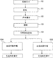
Figure 41 is the flow chart as the assembling procedure of the semiconductor device of an example of the present invention.
Figure 42 is the plane graph on the surface of the basal substrate in the assembling procedure of semiconductor device of Figure 41.
Figure 43 is the plane graph that is connected on the surface of the basal substrate in the assembling procedure of semiconductor device of Figure 42 back.
Figure 44 is the plane graph that is connected on the surface of the basal substrate in the assembling procedure of semiconductor device of Figure 43 back.
Figure 45 is the plane graph that is connected on the surface of the basal substrate in the assembling procedure ground of semiconductor device of Figure 44 back.
Figure 46 is the plane graph that is connected on the surface of the basal substrate in the assembling procedure of semiconductor device of Figure 45 back.
Figure 47 is the plane graph as the back side of the full-scale semiconductor device of another example of the present invention.
Figure 48 is the expansion plane graph of the regional Z1 of Figure 47.
Figure 49 is the plane graph as the back side of the full-scale semiconductor device of another example of the present invention.
Figure 50 is the expansion plane graph of the regional Z2 of Figure 49.
Figure 51 is the plane graph as the back side of the full-scale semiconductor device of another example of the present invention.
Figure 52 is the plane graph as the surface of the semiconductor device of the half-size scale of another example of the present invention.
Figure 53 is the plane graph at the back side of the semiconductor device of Figure 52.
Figure 54 is the plane graph as the surface of the semiconductor device of the half-size scale of another example of the present invention.
Figure 55 is the plane graph as the back side of the semiconductor device of the half-size scale of another example of the present invention.
Figure 56 is the profile as the full-scale semiconductor device of another example of the present invention.
Figure 57 is that the major part of Figure 56 enlarges profile.
Embodiment
In following example, for convenience of explanation, will be divided into a plurality of parts or example when needed describes, but, outside removing under the situation of special instruction, relation between them is a side for the variation of part or all of the opposing party, in detail, the relation of supplementary notes etc., rather than it doesn't matter each other.
In addition, in following example, mentioning under the number of the key element situation of (comprising number, numerical value, amount, scope etc.), remove outside situation about expressing especially and the situation that obviously will be defined in certain number from the principle, also can be that certain number is above or following and be not limited to this certain number.
Also have, in following example, its inscape (also comprising key element step etc.), removing situation about expressing especially and being considered to from the principle obviously is outside the necessary situation etc., self-evident be not necessary can not.
Equally, in following example, when referring to the shape of inscape, position relation etc., to remove situation about expressing especially and be considered to from the principle outside the obviously really not so situation etc., regulation also comprises in fact the approximate or similar relation etc. with this shape etc.This situation also is same for above-mentioned numerical value and scope.
In addition, the part that has same function in being used for illustrating all figure of this example is all given same label, and the explanation of its repetition is omitted.
In addition, in example of the present invention, even if plane graph for the ease of watching, has sometimes also added hacures.
Below, explain example of the present invention with reference to the accompanying drawings.
(example 1)
Fig. 1 is as the semiconductor device of an example of the present invention and the oblique view of auxiliary implement, Fig. 2 (a), (b) oblique view shows surface one side of semiconductor device of Fig. 1 and the outward appearance of the back side one side, Fig. 3 (a) is the plane graph of surface one side of the semiconductor device of Fig. 1, Fig. 3 (b) is the end view of the semiconductor device of (a), Fig. 3 (c) is the back view of the semiconductor device of (a), Fig. 3 (d) is the plane graph of the back side one side of the semiconductor device of (a), Fig. 4 (a) is that the major part of auxiliary implement mounting portion of the semiconductor device long side direction of Fig. 1 enlarges plane graph, Fig. 4 (b) is that the major part of the auxiliary implement mounting portion of semiconductor device short side direction enlarges plane graph, Fig. 5 (a) is the profile of the short direction (A-A line) of the semiconductor device of Fig. 3 (a), Fig. 5 (b) is the expansion profile of the major part of Fig. 5 (a), and Fig. 6 shows the plane graph of the basal substrate of this semiconductor device.
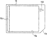
The semiconductor device of this example for example is to can be used as the storage card 1 that the auxilary unit of the electronic installation of information equipment or communication equipment etc. and so on uses.This storage card 1, for example the little thin plate by planar rectangular shape constitutes, its overall dimension, for example long limit is about 24mm, and minor face is about 18mm, and thickness is about 1.4mm.If constant same as before overall dimension, though then in the small-sized electronic installation of for example mobile phone or digital camera etc. and so on, use, but, just become the structure that can in the large-scale relatively electronic installation of portable personal computer etc. and so on, use for also by means of installing metal adapter (auxiliary implement) 2.Exception is called full-scale storage card to the storage card that intactly can use in above-mentioned large-scale electronic installation, the storage card 1 of this example that can use in above-mentioned compact electronic device is called the storage card of half-size scale.
Form the device cap (housing) 3 of the profile of this storage card 1, for example, lightweight from seeking, the viewpoint of ease of processing and flexibility is considered, by ABS resin or PPE (Poly PhenyleneEther, polyphenylene oxide) etc. such resin with insulating properties constitutes, in basal substrate 4, feasible fit on semiconductor chip (below, abbreviate chip as) 5a, 5a, the component mounting face of 5b covers like that and has covered, in device cap 3, form the adapter mounting portion 3a of cross section convexs at 2 local places of two corner parts of the back side of storage card 1 side.This adapter mounting portion 3a, it is the position that cooperates the recess 2a of adapter 2, adopt and to form the surface of device cap 3, side and the back side than surface, side and the back side of the part beyond the adapter mounting portion 3a in the device cap 3, the part formation of the amount of the thickness of slab of lucky recessed adapter 2.In other words, adapter mounting portion 3a is formed and makes its thickness more thinner slightly than the thickness of storage card 1.
In this example, adopt the way of the adapter mounting portion 3a that forms being made to become the cross section convex on the device cap 3 of storage card 1, with comparison under the situation that 3a work in adapter mounting portion is become concavity, can bring up to the mechanical strength of adapter mounting portion 3a more than 2 times or 2 times.
In that adapter mounting portion 3a is done to become under the situation of cross section convex, 2 protuberances must be set on the thickness direction of storage card 1.But, owing to for the thickness of storage card 1, exist a upper limit, so the unlikely thickness of guaranteeing its each protuberance.Because the viewpoint of device cap 3, ease of processing lightweight from seeking and flexibility etc. is considered to be made of resin, so, then can not guarantee mechanical strength if the thickness of the protuberance separately of the recess of formation adapter mounting portion forms too thinly.On the other hand, if the protuberance separately of recess all forms too thickly, the formation of recess self difficulty that will become.To this, adapter mounting portion 3a is done to become under the situation of cross section convex resembling this example, an adapter mounting portion 3 is set on the thickness direction of storage card 1 gets final product.In other words, can focus on a place to the protuberance separately under the situation that in recess, forms adapter mounting portion 3, form thick relatively protuberance.Here, can the thickness of the adapter mounting portion 3a of cross section convex half (d1/2) form thick reach with pit thickness d 2 equal.In other words, can make to become Max (d1/2)=d2 (arriving (c) and Fig. 4 (a)) referring to Fig. 3 (a).Therefore, owing to can form adapter mounting portion 3a thicklyer, so even if also can guarantee mechanical strength with the adapter mounting portion 3a of the part formation of resinous device cap 3.In addition, adapter mounting portion 3a also is easy owing to be the cross section convex so form.In addition,, then can guarantee the equal extent intensity of d1=d2, can make d1 be thinned to d1=d/3 if consider to use the situation that forms adapter mounting portion 3a with device cap 3 same resins.
In addition, in this example, employing is provided with the way of adapter mounting portion 3a in 2 places of two corner parts of the back side of storage card 1 side, owing to adapter 2 is coupled to securely on two ends of long side direction of the back side one side of storage card 1, so can improve stability when being installed on the storage card 1 to adapter 2.
In addition, in this example, in device cap 3, by the adapter mounting portion 3a of above-mentioned two corner parts, place that 3a seizes on both sides by the arms, in other words, in the central authorities of the long side direction of the back side of storage card 1 side, be formed with the thickness of storage card 1 and equate substantially, become to thicker than adapter mounting portion 3a.By means of this, the back side one side that makes storage card 1 with long side direction along storage card 1 all attenuation situation relatively, can improve the mechanical strength of the junction between device cap 3 and the adapter 2.
In addition, in this example, adopt the way of adapter mounting portion 3a being made to become the cross section convex, just can guarantee to be length (length of the short side direction of the storage card 1) L1 of adapter mounting portion 3a fully, in other words, make the recess 2a of adapter 2 be coupled to the length of the direction in the 3a of adapter mounting portion, be again this recess 2a and adapter mounting portion 3a flatness carry out overlapping length.Adapter mounting portion 3a is being done to become under the situation of cross section convex, as mentioned above,, then can not form above-mentioned length L 1 oversizely if the intensity of each protuberance of this recess is guaranteed in consideration.To this, under the situation of this example,, can guarantee the mechanical strength of adapter mounting portion 3a, to above-mentioned length L 1 so can form longly to a certain degree owing to can guarantee the thickness of adapter mounting portion 3a.Here, length ㈠ becomes longer than the thickness d 1 of adapter mounting portion 2a.As mentioned above, have benefited from the way that forms longly to the length L 1 of adapter mounting portion 3, owing to can catch the adapter mounting portion 3a of storage card 1 with the recess 2a of adapter 2 securely, so can guarantee the rigidity of the office, joint portion between storage card 1 and the adapter 2.Therefore, can reduce or prevent to result from bending etc. and make the joint portion disjunction between storage card 1 and the adapter 2 fall such accident.
In addition, in this example, become to asymmetric on the surface of storage card 1 and the state of the adapter mounting portion 3a of place, the back side.Specifically, the width of adapter mounting portion 3a (length of the long side direction of storage card 1) W1, W2 become to asymmetric, its width W 1 separately, the size difference (referring to Fig. 3) of W2.This is because will make the not mistaken cause of installation direction of adapter 2.In other words, because the size of the width W 1 of adapter mounting portion 3a, W2 is different, if the installation direction of adapter 2 made a mistake then the result just becomes to can not mounting adapter 2.By means of this, just can prevent to result from the setup error of adapter 2 and phenomenon that storage card 1 is caused damage or destroys.In addition, since needn't pay special attention to adapter 2 installation direction to mistake, so when can storage card 1 being installed relievedly, can also stably operate to blocking erection unit.
In addition, in this example, near the back side one side at the back side of storage card 1, the central authorities at the long side direction of storage card 1 form adapter pawl mounting portion 3b.This adapter pawl mounting portion 3b is the place that the claw 2b of adapter 2 is tightly hooked, and has pit portion 3b1 and the 3b2 of ditch portion.Pit portion 3b1 adopts the 3b2 of portion that strides over a ditch from the back side of storage card 1 that the way of amount of thickness of slab of the lucky recessed adapter 2 in the back side of device cap 3 is formed.In addition, enter way in the 3b2 of this ditch portion by means of the claw 2b that makes adapter 2, the result just become for storage card 1 and adapter 2 securely in conjunction with being fixed up.
In addition, near the back side one side on the surface of storage card 1, the central authorities at the long side direction of storage card form card and take out ditch 3c.This card takes out ditch 3c, is when above-mentioned electronic installation takes out storage card 1, the ditch that taking-up is assisted.In other words,, adopt the way that lifts finger with the surface of device cap 2 abreast, just can from above-mentioned electronic installation, extract storage card 1 out in that finger touches is taken out to this card under the state on ditch 3c.The depth d 2 of the 2b2 of ditch portion at the back side of said memory card 1 is formed the depth d 3 darker (referring to Fig. 5 (b)) that the card that makes than the surface of storage card 1 takes out ditch 2c.
In addition, the angle of front one side of storage card 1 is cut off for the viewpoint of installation direction that is easy to identification memory card 1 etc.In addition, on the surface of the device cap 3 of storage card 1, near the side front of storage card 1 is formed with and is illustrated in the mark 3d that storage card 1 is installed to the plane trigonometry shape of the direction of insertion when going in the above-mentioned electronic installation.
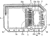
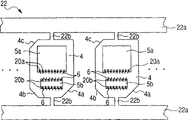
Be assemblied in 2 chip block 5a, the 5a of basal substrate 4 tops of said memory card 1, have same overall dimension, form the flash memory (EEPROM) of same capacity.These chips 5a, 5a are assembled to basal substrate 4 tops under the opposing party's the state on a side top on overlapping.The chip 5a of lower floor joins on the upper surface of basal substrate with bonding agent etc., and the chip 5a on upper strata then joins on the upper surface of chip 5a of lower floor with bonding agent.On the other hand, the chip 5b that controller is used is assembled near basal substrate 4 tops of the chip 5a that memory uses, joins on the upper surface of basal substrate 4 with bonding agent etc. equally.This 3 chip block 5a, 5a, 5b are no matter which all is assembled on the basal substrate 4 making under its interarea (device formation face) state up.
On the interarea separately of the 2 chip block 5a, the 5a that have formed flash memory (EEPROM), be formed with a plurality of bonding welding pads in a row ground on one side along it.In other words, the chip 5a that memory is used adopts on device forms the peripheral part of face and forms bonding welding pad, and along one side one row of these bonding welding pads the monolateral pad mode that is configured.On the other hand, on the interarea of the chip 5b that controller is used, one row ground, every limit forms a plurality of bonding welding pads along for example in opposite directions 2 long limits.
2 chip block 5a, 5a are overlapping each other under unidirectional state, and the bonding welding pad of the bonding welding pad of a side chip 5a and the opposing party's chip 5a is configured contiguously.In addition, the chip 5a on upper strata, its part departs under the state that comes on the direction (directions X) parallel with one side of the chip 5a of lower floor and vertical with it direction (Y direction) and is configured.
Near said chip 5a, 5b basal substrate 4 tops form a plurality of electrodes, with the corresponding electrode of chip 5a, 5a, 5b separately, are electrically connected by the bonding welding wire 6 by gold formations such as (Au).On the bonding welding pad of chip 5a, by above-mentioned electrode be electrically connected to the wiring of the basal substrate 4 on the electrode, be electrically connected on splicing ear 7 that forms on the end of basal substrate 4 and the testing weld pad 8 that forming on the other end.Splicing ear 7 is used as the splicing ear when being installed on the above-mentioned electronic equipment to this storage card 1.And be electrically connected to by through hole 10 on the external connection terminals 9 of lower surface of basal substrate 4.In addition, testing weld pad 8 is used for measuring electrology characteristic in the assembling procedure of this storage card 1. Such chip 5a, 5b, more than half (the removing the periphery of splicing ear 7 and testing weld pad 8 and configuring area thereof) of the component mounting face of bonding welding pad 6 and basal substrate 4, sealing resin 11 linings that for example constituted by epoxy resin etc.
Secondly, above-mentioned adapter 2 is described.Fig. 7 (a) is the plane graph of surface one side of adapter 2, (b) be the end view of the adapter 2 of (a), (c) be the prior figures of the adapter 2 of (a), (d) be the plane graph of the back side one side of the adapter 2 of (a), (e) be (a) adapter 2 claw 2b and support the major part of part 2c to enlarge profile.
In addition, the recess 2a of adapter 2, can adopt the bending two ends of the long side direction of adapter 2 is that the way that makes it to become for substantially U-shaped forms.For this reason, adapter 2 has empty zone to a certain degree on its thickness direction.Also can form hollow form to adapter 2.
As mentioned above, in this example, adapter 2 can adopt way crooked 1 metallic plate or form ditch 2d or hole 2e and so on this metallic plate to form.Do not use the cutting technology of the precision machined metal of needs etc. in other words.In addition, components number is few.Therefore, can reduce the cost of adapter 2.
In adapter 2, from its front, along the short direction (above-below direction of Fig. 7 (a), (d)) of adapter until form 2 above-mentioned ditch 2d that extend abreast till the median-plane location, way of its short direction bandedly.By this ditch 2d flatness of 2 on the part (the long side direction central authorities of adapter 2) of seizing on both sides by the arms, form above-mentioned support part 2c.On the other end of supporting part 2c, become to forming above-mentioned claw 2a.Support part 2c to have function, be formed rectangular shape from the plane as leaf spring (elastomer), in addition, from section from adapter 2 surface towards the back side little by little bending like that, in other words, at the state compacted under that makes it to have deflection.As mentioned above, adopt the raising make the way of supporting part 2c to have deflection seek elastic force and as the raising of elastomeric durability.As mentioned above, supporting part 2c to it is desirable to its length is designed to purpose and has appropriate flexible length for making it.
In addition, near the side of the back side of adapter 2, formed the opening of hole 2e.Under the state that adapter 2 is assembled on the above-mentioned memory 1, after being assembled to it in the electronic installation, when from electronic installation, taking out this storage card 1, when this taking-up can not successfully be carried out etc., just can be hooked to taking-up storage card 1 in the 2e of this hole to pawl or instrument.Hole 2e also can make to become the impression shape of ditch etc. and not do to become the hole.
Fig. 8 (a) shows the state after being assembled on the said memory card 1 to above-mentioned adapter 2, and Fig. 8 (a) is the plane graph on the surface of its storage card 1 and adapter 2, (b) is the end view of (a), (c) is the plane graph at the back side of (a).In addition, Fig. 9 in order to compare, shows above-mentioned full-scale storage card 50.Fig. 9 (a) is the plane graph on the surface of storage card 50, (b) is its end view, (c) is the plane graph at its back side.Have again, Figure 10 (a) show storage card 1 adapter pawl mounting portion 3b, and the claw 2 of adapter 2 between the profile of bonding part, (b) be the profile of the bound fraction between the recess 2a of the mounting portion 3a of storage card 1 and adapter 2.
The claw 2b of adapter 2, in the last direction of Figure 10 (a), in other words, with device cap 3 direction in opposite directions on have under the state of elastic force, be embedded into securely in the 3b2 of ditch portion of adapter pawl mounting portion 3a of storage card 1.By means of this, just can positively combine storage card 1 and adapter 2.And, the adapter mounting portion 3a of embedding storage card 1 in the recess 2a of adapter 2.By means of this, just can have good stability ground storage card 1 and adapter 2 are combined.
Will be when storage card 1 takes off adapter 2, be from the support part 2c of the direction pushing adapter 2 at the one side direction back side, surface of adapter 2, the claw 2b that takes away the top of supporting part 2c from the adapter pawl mounting portion 3b of storage card 1 gets final product.Therefore, even if also can take away adapter 2 simply with a hand, it takes off operation and can extremely easily carry out for this reason, and the length of the support part 2c that can observe from the surface of storage card 1 when it assembles it is desirable to the sort of degree that people's finger can enter.In addition, support part 2c, as mentioned above,, will get back to original shape after taking away adapter 2 owing to have elasticity.
An example of the mould that uses when secondly, the formation of device cap 3 of said memory card 1 being described.Figure 11 is the profile of this mould 15, shows the profile with the same position of Fig. 5.In addition, Figure 12, the major part that is Figure 11 enlarges profile, (a) be the back side one side and the profile same position of Fig. 5 (b) of device cap 3, (b) be the profile at the position corresponding, (c) be front one side and the profile same position of Fig. 5 of device cap 3 with the adapter mounting portion 3a of the back side one side of device cap 3.
On the part that counterdie 15a and patrix 15b are piled up, form and be used for the cavity 15c of moulding device cap 3.In this example, having become towards the corner part α 1~α 11 of the mould 15 (counterdie 15a and patrix 15b) of this cavity 15c etc. is 90 degree or more than 90 degree (referring to Figure 12).By means of this, just can easily carry out the moulding of device cap 3.If above-mentioned angle [alpha] 1~α 11 to 90 degree are little, then after 3 moulding of device cap, device cap 3 just is difficult to peel off from mould 15 and since just become for or only form a device cap 3 at every turn, perhaps need special mould, so cost increases.With respect to this, in this example, have benefited from that work such as angle [alpha] 1~α 11 becomes 90 degree or more than 90 degree, owing to can not produce such shortcoming, be state that can volume production so just become.In addition, do not need special mould yet.Therefore, can reduce the cost of storage card 1.With the angle of the corner part at surface, side and the back side of the device cap 3 of such mould 15 moulding, becoming is 90 degree or more than 90 degree.
In addition, in this example, this squarely becomes deeplyer than the degree of depth (equal with thickness d 7 substantially) at the cavity 15c at the patrix 15b one side place of the outer surface that forms device cap 3 in the degree of depth (thickness is d5+d6 substantially) of the cavity 15c at the counterdie 15a one side place of the medial surface that forms device cap 3.Therefore, on the part that is equivalent to thickness d 6, more than half cast gate of using to counterdie 15a one side inflow resin that forms.Why dark this side of the degree of depth of the cavity 15c of counterdie 15a one side is, is because this side of inboard (bottom surface one side) of the cavity 15c of counterdie 15a one side is concavo-convex many with step, if there is not capacity to a certain degree, and the cause of potting resin satisfactorily just.In addition, in thickness d 5 in d7, thickness d 6 size maximums.This is because will improve the cause of the fillibility of the resin that flows into from cast gate in cavity 15c.In other words, if this thickness d 6 is too thin, just can not resin be flowed in cavity 15c by cast gate.Here, thickness d 5 for example is about 0.5mm, and thickness d 6 for example is about 0.6mm, and thickness d 7 for example is about 0.3mm.
In this example, the way moulding of employing potting resin in the cavity of such mould 15 after the device cap 3, cover this device cap 3, make the component mounting face of the basal substrate 4 that loads chip 5a, 5b is covered, to make the said storage card 1 in top.
Secondly, the example of assemble method of the semiconductor device of this example is described.Figure 13 is the key diagram that is used for illustrating this example, (a) is all plane graphs of storage card 1, (b) is the basal substrate 4 of storage card 1 is assembled into all plane graphs under the situation about using on the full-scale storage card.The part of band shade is represented the plane of basal substrate 4.
In this example, in full-scale storage card 1A, maintain the original state and use the basal substrate 4 (basal substrate 4 of the state of fit on chip 5a etc.) that in the assembling of the storage card 1 of half-size scale, uses unchangeably.In other words, make to become the storage card 1 that makes total planar dimension different, the part of 1A.
Because the cost of storage card is more than half for the cost of basal substrate 4 occupies,, be effective aspect the cost that reduces storage card 1 so reduce the cost of basal substrate 4.But, in the storage card 1 of half-size scale and full-scale storage card 1a, separately make under the situation of basal substrate 4, owing to need manufacturing process, manufacturing installation and personnel etc. separately respectively,, the cost of storage card raise so will cause the increase of the cost of basal substrate 4.With respect to this, adopt to make storage card 1, the total way of 1A since half-size scale and full-scale in no longer need to be provided with separately manufacturing process, manufacturing installation and the personnel of basal substrate 4, so can reduce the cost of storage card 1,1A significantly.
Under the situation that adopts such assemble method, shown in Figure 13 (b), on full-scale storage card 1A, assemble the basal substrate 4 of half or half following area of plane of the area of plane of its device cap 16.
(example 2)
Figure 14 is the semiconductor device of another example of the present invention and the oblique view of auxiliary implement, Figure 15 (a), (b) oblique view shows surface one side of semiconductor device of Figure 14 and the outward appearance of the back side one side, Figure 16 (a) is the plane graph of surface one side of the semiconductor device of Figure 14, Figure 16 (b) is the end view of the semiconductor device of (a), Figure 16 (c) is the back view of the semiconductor device of (a), Figure 16 (d) is the plane graph of the back side one side of the semiconductor device of (a), Figure 17 (a) is the plane graph on the surface of the semiconductor device of Figure 14 and auxiliary implement, (b) being the end view of (a), (c) is the plane graph at the back side of (a).
This example, remove the shape of the binding site between storage card 1 and the adapter 2 and above-mentioned example 1 different outside, with above-mentioned example 1 be same.In other words, the side of the adapter mounting portion 3a of storage card 1 is formed the side that makes it with storage card 1 and becomes and be same plane.In other words, the lateral parts of adapter mounting portion 3a is not dented.In addition, on the side of storage card 1, also partly form such ditch 2a1: the lateral parts of above-mentioned adapter mounting portion 3a enters in the part of the recess 2a that will be coupled to the adapter 2 on the 3a of this adapter mounting portion.
Even if under these circumstances, as shown in figure 17, also can be under the state of neat and tidy, adapter 2 is installed on the storage card 1 and can combining between storage card 1 and adapter 2 do not produce concavo-convex or shortcoming on the side.
In this sample example, also can obtain the effect same with above-mentioned example 1.
(example 3)
Figure 18 shows the plane graph as the back side one side of the semiconductor device of another example of the present invention.In this example, in the back side of storage card one side, near the long side direction along storage card 1 3a of adapter mounting portion disposes a plurality of splicing ears 17 regularly with lining up.Splicing ear 17 is arranged on the back side one side of basal substrate 4, is electrically connected by the wiring of basal substrate 4 and the memory circuitry that forms in basal substrate 4 tops.The test that this splicing ear 17 is above-mentioned memory circuitries is used or function is appended the terminal of usefulness.
(example 4)
At first, the problem that the inventor in the technology that the inventor studied at first finds is described to Figure 23 with Figure 19.
Figure 19 and Figure 20 show the surface (component mounting face) of above-mentioned basal substrate 4 and the plane graph of the back side (external connection terminals formation face) respectively.Basal substrate 4 planar rectangular shape ground forms, and an one corner part corresponding site carries out chamfering to the turning and forms chamfered part (the 3rd chamfered part) 4a.Chamfered part 4a is formed along the chamfering that goes up location (index) usefulness that forms on the top, front of storage card (installation end).
Device cap (the 1st housing) 16 the surface and the plane graph at the back side of the above-mentioned full-scale storage card 6 that Figure 21 and Figure 22 show the inventor respectively and studied.This device cap 16 can be with the same formation such as resin of the device cap used with above-mentioned half-size scale 3.In device cap 16, form chamfered part (the 2nd chamfered part) 16a of above-mentioned location usefulness at the side place of the corner part of the front of storage card one side.This chamfered part 16a is provided with for the viewpoint of the installation direction that is easy to discern full-scale storage card.
In addition, at the back side of device cap 16, form ditch 16b in the front of said memory card one side.This ditch 16b is to be used for basal substrate 4 is installed to the ditch of device cap 16, be formed make occupy near the top of device cap 16 till the shorter position of half of the long side direction of device cap 16.The flat shape of ditch 16b and size are used and basal substrate 4 same flat shapes, and, use than the bigger size of basal substrate 4 to form, so that can take in basal substrate 4 and cooperate well.Therefore, in ditch 16b, a side's of front one side of device cap 16 corner part chamfering forms chamfered part 16b1.In addition, the long limit of the long side direction of the device cap 16 within 2 long limits of ditch 16b central authorities one side formation and 2 minor faces of ditch 16b intersect squarely.In addition, in the periphery, formation is inboard thicker than it in the zone of ditch 16b, and, than the thinner step part 16e in the outside of ditch 16b.Be engraved in a plurality of contact pin vestige 16f on this step part show with mould molding after the device cap 16 when from mould, taking out ejector (ejector) vestige that contact pin contacted.
In addition, in the surface and the back side of this device cap 16, near the side, form card and take out ditch 16c1,16c2 overleaf.This card takes out ditch 16c1,16c2 and has the ditch that card with explanation in above-mentioned example 1 takes out ditch 3c (referring to Fig. 1 etc.) said function.The degree of depth of the 16c2 of ditch portion of a side forms deeplyer than the card taking-up ditch 16c1 in a surperficial side overleaf.This card takes out ditch 16c1,16c2 also can only be arranged on either party.In addition, on the surface of device cap 16, near an in front side, formation is illustrated in the mark 16d of the plane triangle shape of the direction of insertion when being installed in the above-mentioned electronic installation to full-scale storage card.In addition, more than half part on the surface of device cap 16, the shallow pit 16g of the rectangular shape of formation plane fillet.This pit 16g is to be used for pasting the pit that shows all information labels such as storage card classification.
Figure 23 shows the plane graph at the back side of the full-scale storage card 1A after being installed in the ditch 16b of Figure 21 and device cap 16 shown in Figure 22 to Figure 19 and basal substrate 4 shown in Figure 20.Basal substrate 4 is incorporated in one-sided substantially half the zone of long side direction of device cap 16, and installs well.
The inventor has carried out bending strength test to full-scale storage card 1A shown in Figure 23.This bending strength test for example carries out as described as follows.At first, under the state of the upper surface of testing stand, storage card 1A mounting is arrived the testing stand top at the back side that makes storage card 1A.At this moment, do to become make near the two ends of the long side direction of storage card 1A 2 in the localities, between the back side of storage card 1A and testing stand upper surface, exist support member, between the upper surface of the back side of storage card 1A and testing stand, form the gap of given size.Under this state, adopt and add that the way of the loading of ormal weight makes storage card 1A deflection estimate breakdown strength on the surface of storage card 1A, for long side direction central authorities.
The inventor finds for the 1st time: the result who carries out this test, such storage card 1A shown in Figure 23, in full-scale storage card, and the storage card that the work of the planar dimension between basal substrate and the device cap is become the structure of equal extent compares, a little less than the bending strength, in the back side of storage card 1A central authorities, boundary member (interstitial fraction) between device cap 16 and basal substrate 4 is located basal substrate 4 and is peeled off, perhaps the long limit that forms with long side direction central authorities one side of the device cap 16 within the long limit of the ditch 16b of device cap 16 and 2 decussate parts of minor face of ditch 16b are starting point, the shortcoming that cracks on device cap 16 and so on.
So, in this example, in the only about half of full-scale storage card of the planar dimension that the planar dimension of basal substrate work is become the device cap, make to become the structure that improves above-mentioned bending strength.Specifically, for example as described below.
Figure 24 and Figure 25 show the surface (component mounting face) of the basal substrate 4 of this example 4 and the plane graph of the back side (outside terminal formation face) respectively.In the basal substrate 4 of this example 4, remove outside the above-mentioned chamfered part 4a, make the turning chamfering at 2 suitable positions of corner part form chamfered part (the 1st chamfered part) 4b, 4c.This chamfered part 4b, 4c chamfering are littler than chamfered part 4a, form with same size and shape and make mutual left-right symmetric, in addition, with the situation of explanation in above-mentioned example 1, Figure 19 and Figure 20 etc. be same.
Figure 26 and Figure 27 show the surface of the device cap 16 that the full-scale storage card that loads Figure 25 and basal substrate 4 shown in Figure 26 uses and the plane graph of the back side (basal substrate installed surface) respectively.The device cap 16 of this example 4, the shape of ditch (the 1st ditch) 16b of installation basal substrate 4 is different with the said shape in top.In addition formation and is same in above-mentioned example 1, Figure 21 and formation illustrated in fig. 22.In other words, in this example 4, the flat shape of ditch 16b and size are used to form with its basal substrate 4 same flat shapes and than the bigger planar dimension of basal substrate 4 to make and can take in Figure 24 and basal substrate 4 shown in Figure 25 and can cooperate well.Therefore, long limit 16b2 that long side direction central authorities one side of the device cap 16 within 2 long limits of ditch 16b in this case forms and 2 minor face 16b3, the 16b3 of ditch 16b do not carry out right-angle crossing, its part of intersecting is originally then carried out chamfering, forms chamfered part (the 1st chamfered part) 16b4,16b5.In other words, ditch 16b becomes and is such structure: its long limit 16b2 and minor face 16b3 to each other, by being configured to make chamfered part 16b4,16b5 optionally change for their diagonal cross.Perhaps, doing becomes such structure: in ditch 16b, originally will be in 2 corner part offices that the central side of the long side direction of device 16 forms, and enhancing part 16h1, the 16h2 of configuration right angle 2 equilateral triangle shapes under the state that the right angle part is coincide.The chamfering that constitutes of this chamfered part 16b4,16b5 must be littler than chamfered part 16a, and form left-right symmetric each other with same size and shape.
Figure 28 shows the plane graph at the back side of the full-scale storage card 1A after being installed on the device cap 16 of Figure 26 and Figure 27 to Figure 24 and basal substrate 4 shown in Figure 25, and Figure 29 shows the A1-A1 line profile of Figure 28.In this example 4, basal substrate 4 makes its surface towards the ditch 16b at the back side of device cap 16 side, and chamfered part 4b, the 4c that makes basal substrate 4 is installed in the ditch 16b respectively with under chamfered part 16b4, the 16b5 state in opposite directions of ditch 16b.Basal substrate 4, the state that touches with its surperficial outer peripheral portion on the step part 16e in the ditch 16b of device cap 16 is supported.
In this example 4, owing to can form the contact length between basal substrate 4 and the ditch 16b longer than situation shown in Figure 23, so can improve the bond strength between basal substrate 4 and the device cap 16.Can adopt in addition chamfered part 4b, 4c are set on basal substrate 4, chamfered part 16b4,16b5 are set on ditch 16b, the way of the right angle part that is easy to concentrate of eliminating stress, dispersive stress.By means of these, when carrying out above-mentioned bending strength test, just can suppress or prevent peeling off of basal substrate 4, in addition, can also suppress or prevent on device cap 16, to crack.
In addition, the structure that improves above-mentioned bending strength does not need to append other new member, only is the simple structure that the corner part of the ditch 16b of the corner part of basal substrate 4 and device cap 16 is carried out chamfering, and its formation is easy.Therefore, can provide the reliability height and can not influence productive full-scale storage card 1A.
In addition, the full-scale storage card 1A of this example 4 is also favourable structure in the electrostatic breakdown test even if be made to.In this electrostatic breakdown test, under the state that storage card is installed on the experimental rig, one side adds static from the back side.In full-scale storage card, under the situation of the structure that the planar dimension of basal substrate and device cap work is become equal extent, because till being set to basal substrate near the back side one side of storage card always, thus the conductive path till from the back side one side of storage card to the chip of front one side apart from lacking.With respect to this, under the situation of the storage card 1A of this example 4, from its back side to long side direction substantially about half till form with the device cap 16 of insulating properties, because the distance of the conductive path till from its back side one side to the chip of front one side, so become in the electrostatic breakdown test, being difficult to produce the structure of destruction.
Have again, in full-scale storage card 1A, in the planar dimension of basal substrate 4 is made to the structure about half of the planar dimension of device cap 16, with the planar dimension of basal substrate and full-scale device cap is made to become the structure ratio that equates, owing to can reduce the area of basal substrate 4 and the volume of sealing resin 11, so storage card 1A can form gently.Particularly under the situation of the storage card 1A of this example 4 because as mentioned above also to basal substrate, corner part carry out chamfering, so can advance lightweight.Therefore, can improve the Portability of full-scale storage card 1A.
Figure 30 is to Figure 32, shows result's the key diagram of the bending strength test of storage card 1A shown in Figure 23.As can be known in the storage card 1A of this structure, locate at the basal substrate 4 and the boudary portion between the device cap 16 (position b3, b4) of the middle body substantially of the long side direction of device cap 16, bending strength sharply and rectangular shape ground descend very greatly.Label b1 makes the position relation that can understand in Figure 32 to each other at Figure 30 show the position like that to b4 in addition.
On the other hand, at Figure 33 in Figure 35, the result's of the bending strength test of the storage card 1A shown in Figure 28 of showing at this example 4 waits key diagram.As can be known, in this example 4 storage card 1A, the basal substrate 4 and the boudary portion between the device cap 16 (position b5, b6, b4) of central authorities substantially at the long side direction of device cap 16 are located, the decline of bending strength is milder, and simultaneously the ratio of its minimum and Figure 31 and Figure 32 becomes and is high value.In other words, can improve the bending strength of full-scale storage card 1A.
Secondly according to Figure 36 and Figure 37 the definition of the size aspect of the full-scale storage card 1A of this example 4 is described.
Figure 36 shows the plane graph at the back side of the device cap 16 of this example 4.Length (in other words, the size of the short direction of the basal substrate 4 substantially) X1 of the short direction of ditch 16d is than the also little (X1<X/2) of half of the total length X2 of the long side direction of device cap 16.This is because will make to become the cause that can use basal substrate 4 full-scale and this two side of half-size scale.In other words, if width X1 equal total length X2 half or also longer than half, then in the storage card 1 of the half-size scale of above-mentioned example 6 explanations, just no longer can use this basal substrate.Length X 1 for example is about 14.5mm, and total length X2 for example is about 32mm.
In addition, in this example 4, in chamfered part 16b4,16b5, the length Y1 of the short direction of the length X 3 of the long side direction of device cap 16 and device cap 16 is made to become equal (X3=Y1).Therefore, angle θ is 45 degree.In theory, be because this situation can integrally improve the cause of the bending strength in the corner part zone.In addition, if adopt the inventor's research, even if supposition Y1>X3 also can obtain good result on bending strength.Length X 3, Y1 for example are about 2mm.
The length L 2 of chamfered part 16a, than length X 3, Y1 also long (L2>X3, Y1).This is because when length X 3, Y1 are too big, and it is too small that the area of basal substrate 4 will become, become can not the mounting chip cause.Length L 2 for example is about 5.66mm.
In addition, this length X 3, Y1 than thickness d 8, d9, d10 big (X3, Y1>d8, d9, d10).This is because if length X 3, Y1 are littler than thickness d 8, d9, d10, then because of the too little cause that can not obtain above-mentioned bending strength fully of chamfering amount.Thickness d 8 for example is about 1mm, and thickness d 9, d10 for example are about 0.6mm.
In addition, Figure 37 shows the expansion profile of major part of the storage card 1A of this example 4.The gross thickness of storage card 1A is equivalent to the thickness d 11 of device cap 16.This thickness d 11 is equal to or greater than thickness d 12 (d11 〉=d12).Thickness d 12 is the thickness till from the surface of device cap 16 to the back side of basal substrate 4.The reason of above-mentioned size regulation is: if this thickness d 12 is also thicker than thickness d 11, then do not conform with the specification of storage card.The degree of depth of depth d 13 expression ditch 16b.Thickness d 11 for example is that thickness d 12 for example is equal to or less than about 1.4mm about 1.4mm.Depth d 13 for example is about 1.04mm, and thickness d 14 for example is about 0.28mm.
Secondly, an example of the mould that uses during to the formation of the device cap 16 of the full-scale usefulness shown in Figure 29 grade at Figure 26 with Figure 38 explanation.Figure 38 is the profile of this mould 15.Its structure is identical substantially with the structure that illustrates in Figure 11 of above-mentioned example 1 and Figure 12 (a), (c).Length till different is from the central authorities substantially of the long side direction of cavity 15c to the part of the back portion that forms device cap 16 is longer than the length of Figure 11 and part shown in Figure 12.
Secondly, the configuration example of chip of the basal substrate 4 of this example 4 is described with Figure 39 and Figure 40.Figure 39 and Figure 40 show the plane graph on the surface (component mounting face) of the basal substrate 4 of this example 4.
In this example 4, on the surface of basal substrate 4, be mounted with chip 5b that chip 5a that 1 memory uses and 1 controller use etc.The long side direction (disposing in other words, the direction of a plurality of external connection terminals 9 (referring to Figure 25, Figure 28)) that these 2 chip 5a, 5b are configured to along basal substrate 4 is arranged.The chip 5a that relatively big memory is used is configured on the chamfering 4a of location one side position far away.The chip 5b that relatively little on the other hand controller is used then is configured in apart from the near side of chamfered part 4a of location one side.Owing to such configuration, can realize small-sized and jumbo storage card.
In the chip 5a that above-mentioned memory is used, form for example memory circuitry of 16M, 32 bytes of memory capacity.This side of chip 5a that memory is used is made to more approaching foursquare shape than controller with chip 5b.The length L 3 on one side of the chip 5a that memory is used is formed to such an extent that one side length L 4 of extending on long side direction of the chip 5b that uses than controller is longer.On the interarea of the chip 5a that memory is used, near on one side, on one side dispose a plurality of bonding welding pad 20a along this.The chip 5a that memory is used makes it dispose long side direction central authorities one side that is configured in basal substrate 4 of a plurality of bonding welding pad 20a one side be loaded, and is configured in chip 5b one side that controller is used in other words.This bonding welding pad 20a is electrically connected by the wiring of bonding welding wire 6 with the surface of basal substrate 4.
On the other hand, on the interarea of the chip 5b that controller is used, near 2 long limits, dispose a plurality of bonding welding pad 20b along this length limit.The chip 5b that controller is used is loaded in the surperficial top of basal substrate 4 and makes its long limit become to parallel for disposing memory one side with a plurality of bonding welding pad 20a of chip 5a.This bonding welding pad 20b is electrically connected by the wiring of bonding welding wire 6 with the surface of basal substrate 4.Such chip 5a, the configuration of 5b also can be applied to above-mentioned example 1 to example 3.
In addition, top one side (having formed the side of chamfered part 4a) at the long side direction on the surface of basal substrate 4 forms by means of the gold-plated metal level 21 that forms that waits.This metal level 21 is parts of the cast gate of configuration mould when sealing chip 5a, 5b.In other words, make when forming sealing resin 11 (referring to Figure 29) that the configuring area of the chip 5b that uses by controller from these metal level 21 1 sides flows into resin to memory with the configuring area of chip 5a.
Secondly, the example of assemble method of the semiconductor device of this example 4 is described.This assembling procedure is identical with operation illustrated in fig. 13 at above-mentioned example 1.Here the flow chart along Figure 41 illustrates this assembling procedure with Figure 42 to Figure 46.
At first, prepare the sort of basal substrate organizator 22 shown in Figure 42.On the framework 22a of this basal substrate organizator 22, a plurality of basal substrates 4 are coupled together by the fine linking portion 22b in 2 minor face central authorities that are connected to each basal substrate 4.In this stage, form framework 22a, linking portion 22b and basal substrate 4.In addition, chamfered part 4b, the 4c of basal substrate 4 have also been formed.Then, as shown in figure 43, chip 5a, 5b (operation 100 of Figure 41) are loaded in the surperficial top of each basal substrate 4 of basad substrate organizator 22.At this moment, relatively big memory is loaded into apart from chamfered part 4a place far away with chip 5a,, is loaded into apart from the near place of chamfered part 4a relatively little controller chip 5b.Then, implement for example plasma clean operation (operation 101 of Figure 41) that purpose is the cleaning surfacesization of the wiring that makes basal substrate 4 and chip 5a, 5b, electrode (comprising bonding welding pad 20a, 20b).The purpose of this operation is: adopt the way that the surface that forms thinly Gold plated Layer is cleaned, make that the connection status between the welding wire and Gold plated Layer becomes well when being connected on the bonding welding wire operation of this operation back.
Then, as shown in figure 44, in each basal substrate 4, by bonding welding wire 6 wiring and the electrode of bonding welding pad 20a, the 20b of chip 5a, 5b and basal substrate 4 are electrically connected (operation 102 of Figure 41).Then, as shown in figure 45, in each basal substrate 4, chip 5a, 5b and bonding welding wire 6 etc. sealed (operation 103 of Figure 41) with continuous automatic mold casting.After above-mentioned welding wire bond sequence, before the die casting operation, also can implement above-mentioned purified treatment to basal substrate 4 for the viewpoint of the cementability that improves sealing resin.Then, as shown in figure 46, adopt the way of cutting off linking portion 22b, basal substrate 4 is separated (operation 104 of Figure 41) from basal substrate organizator 22.After handling in this wise, form basal substrate 4.
Then, under the situation of the storage card 1A that will make full-scale (FS), above-mentioned basal substrate 4 is installed in the ditch 16 of Figure 26 and device cap 16 shown in Figure 27 the back and fixes (the operation 105A of Figure 41) with bonding agent etc.On the other hand, under the situation of the storage card 1 of making half-size scale (HS) (or minification (RS)), then fix (the operation 105B of Figure 41) in the ditch at the back side of the device cap 3 that illustrates in Fig. 5 etc. of Fig. 1 that basal substrate 4 is installed at above-mentioned example 1 (flat shape of the ditch here is formed in the shape that Figure 27 illustrates in Figure 29) and with bonding agent etc.
As mentioned above, in this example, can make full-scale and half-size scale so 2 kinds storage card 1,1A with 1 basal substrate 4.In other words because the manufacturing process of the storage card 1 of full-scale and half-size scale, 1A and member can commonization of part, so with situation about making separately under compare, the reduction of the simplification of manufacturing process, the shortening of manufacturing time and manufacturing cost just becomes possibility.
(example 5)
In this example 5, illustrate in the full-scale storage card about half of the planar dimension of the planar dimension of basal substrate being made become the device cap, improve the variation of the structure of above-mentioned bending strength.
Figure 47 shows the plane graph at the back side of the full-scale storage card 1A of example 5, and Figure 48 shows the expansion plane graph of the regional Z1 of Figure 47.In this example 5, in basal substrate 4, near two corner parts of long side direction central authorities one side that is positioned at full-scale device cap 16, form the concavo-convex 4d of fine rectangular shape, near the corner part of the ditch 16b of corresponding with it device cap 16, also form the concavo-convex 16b7 of fine rectangular shape, make it to be coupled to well in the fine concavo-convex 4d of basal substrate 4.Concavo-convex 4d, 16b7 that this is fine are formed left-right symmetric in Figure 47.In addition with in example 1 to 4 explanation be same.Above-mentioned concavo-convex 4d, 16b7 also can be arranged on long limit one side of the long limit 16b2 of ditch 16b and corresponding with it basal substrate 4.
In this example 5,,, can improve above-mentioned bending strength so can suppress or prevent the crackle of device cap 16 or peeling off of basal substrate 4 owing to, also increase the contact area between basal substrate 4 and the device cap 16 in the relatively weak corner part office of intensity.
(example 6)
In this example 6, illustrate in the full-scale storage card about half of the planar dimension of the planar dimension of basal substrate being made become the device cap, improve another variation of the structure of above-mentioned bending strength.
Figure 49 shows the plane graph at the back side of the full-scale storage card 1A of example 6, and Figure 50 shows the expansion plane graph of the regional Z2 of Figure 50.In this example 6, same with above-mentioned example 5, be positioned at basal substrate 4 and with it near the corner part of the ditch 16b of corresponding device cap 16, also forming fine concavo-convex 4d, 16b7.Different with above-mentioned example is to form taper on the side of each fine concavo-convex 4d, 16b7.In this case, with under the situation of example 5 relatively, the fine easier cooperation of concavo-convex 4d of the fine concavo-convex 4d of basal substrate 4 and the ditch 16b7 of device cap 16.In addition with in example 1 to 5 explanation be same.Above-mentioned concavo-convex 4d, 16b7 also can be arranged on long limit one side of the long limit 16b2 of ditch 16b and corresponding with it basal substrate 4.
(example 7)
In this example 7, illustrate in the full-scale storage card about half of the planar dimension of the planar dimension of basal substrate being made become the device cap, improve another variation of the structure of above-mentioned bending strength.
Figure 51 shows the plane graph at the back side of the full-scale storage card 1A of this example 7.In this example 7, in basal substrate 4, long limit in central authorities' one side of the long side direction that is positioned at full-scale device cap 16, near two corner parts of vertical with it minor face, form jagged fine concavo-convex 4d, on the long limit of the ditch 16b of corresponding with it device cap 16 and minor face, also form fine jagged concavo-convex 16b7, make it to be coupled to well in the fine concavo-convex 4d of basal substrate 4.In addition with in example 1 to 4 explanation be same.Therefore, in this example 7, also can obtain effect with the same bending strength aspect of above-mentioned example 4 to 6.
(example 8)
In this example 8, use in above-mentioned example 4 is described at the storage card of the half-size scale of the basal substrate shown in Figure 24 and Figure 25 etc.
Figure 52 and Figure 53 divide the surface of storage card 1 of half-size scale of another edition of a book example 8 and the plane graph at the back side.On the front of the device cap (the 2nd housing) 3 of storage card 1, a side corner part chamfering forms the chamfered part 3e of above-mentioned location usefulness.This chamfered part 3e is provided with for the feasible viewpoint that is easy to the installation direction of identification memory card 1.In addition, on the surface of device cap 3,, form the back side from storage card 1 to the sagittate mark 3d2 that extends previously in chamfered part 3e one side.This mark 3d2 represents storage card 1 is installed to direction of insertion when going in the above-mentioned electronic installation.In the storage card 1 of the half-size scale of this example 8, though with top of its short direction for being installed to anteriorly in the electronic installation, but, because such fixed idea is arranged in general: storage card is that the front is installed in the electronic installation with the top of its long side direction, so will represent mark 3d more greatly in order to avoid produce mistake.In addition, on the surface of device cap 3, on the zone of leaving chamfered part 3e, forming shallow ditch 3f this shallow ditch 3f of plane square shape, is the zone of label of the content of the stickup record data that show storage card 1.
In addition, on the back side of the device cap 3 of this example 8, formation and its basal substrate 4 same flat shapes and planar dimension be than bigger ditch (the 2nd ditch) 3g of basal substrate 4, makes can take in Figure 24 and basal substrate 4 shown in Figure 25 and can cooperate well.Therefore, among the ditch 3g in this case, near the long limit 3g1 the back side of storage card 1 intersects with 2 minor face 3g2, the 3g2 out of plumb of ditch 3g, forms chamfered part (the 1st chamfered part) 3g3,3g4 after the part chamfering that it intersects originally.About the structure (comprising chamfered part 3g3,3g4) of this ditch 3g, be the same with the ditch 16b of full-scale device cap 16 of explanation in above-mentioned example 4.Therefore, no matter can as fired basis substrate 4 in half-size scale in full-scale.In addition, the installment state of basal substrate 4 in ditch 3g also with in above-mentioned example 4 explanation be identical.Extension ditch when in addition, the above-mentioned ditch 3b2 of portion at the back side of device cap 3 also plays a part storage card taken out from electronic installation.
(example 9)
In this example 9, illustrate according to the specification of storage card to change reply example under the situation of number of external connection terminals 9 at the back side.
Figure 54 shows the example under the number of external connection terminals 9 of the storage card 1 that makes this example 9 situation consistent with the number of the external connection terminals of SD card (Panasonic, Toshiba, Sun Dsik).On the back side (back side of basal substrate 4) of storage card 1, configuration adds up to 9 external connection terminals 9.In addition, Figure 55 shows the example under the number of external connection terminals 9 of the storage card 1 that makes this example 9 situation consistent with the number of the external connection terminals of IC-card.The part of the external connection terminals 9 that adds up to 13 is become be 2 to be configured, the problem that has nothing special no matter any situation can be tackled capablely.
(example 10)
In this example 10, illustrate in the full-scale storage card about half of the planar dimension of the planar dimension of basal substrate being made become the device cap, improve another variation of the structure of above-mentioned bending strength.
Figure 56 shows the profile of the full-scale storage card 1A of this example 10, and Figure 57 is that the major part of Figure 56 enlarges profile.In this example 10, on the long limit 16b2 of the ditch 16b of device cap 16, the brim of a hat part 16i is set integratedly.The brim of a hat part 16i both can extend along long limit 16b2, also can form in the part that is distributed to long limit 16b2.Employing resembles way that the brim of a hat part 16i is set in this wise (in other words, adopting the way that reinforcement is set), formation recess 16j on the side of long limit 1,6b2 one side of ditch 16b.So, be coupled in this recess 16j, just become to firmly fixing the structure of basal substrate 4 by means of the part of the back side one side that makes basal substrate 4.Here, for basal substrate 4 is coupled in the recess 16j, the part of the back side one side of basal substrate 4 is because of being etched away half attenuation.Have benefited from such structure, owing to can improve above-mentioned bending strength, so can suppress or prevent peeling off or the destruction of device cap 16 of basal substrate 4.Under the situation of the structure that adopts this example 10, though also chamfered part 16b4,16b5 can be set on ditch 16b,, have benefited from being provided with chamfered part 16b4,16b5, can further improve bending strength.In addition, in this case, also the brim of a hat part 16i can be set in the place of its chamfered part 16b4,16b5.
More than, though specifically understand the invention of inventing according to example by the inventor,, the present invention is not limited to above-mentioned example, and is self-evident, in the scope that does not deviate from main idea of the present invention all changes can be arranged.
For example, the shape or the number of the support of adapter part are not limited to above-mentioned example, and all changes can be arranged.
In addition, chip is removed outside the connection of welding wire bonding mode, also can adopt the connected mode of using prominent point electrode.
In the above description, though mainly at built-in as situation about using in the storage card of invention for the flash memory that utilizes the field (RRPROM) of its background that is undertaken by the inventor is illustrated, but, be not limited thereto, for example also can in the storage card of for example other memory circuitry of built-in SRAM (static RAM), FRAM (ferroelectric RAM) or MRAM (magnetic RAM) etc. and so on, use.
Claims (11)
1. semiconductor device, on the part of the resin system housing that the component mounting face of the substrate that will be mounted with semiconductor chip covers, the mounting portion of the cross section convex that can cooperate with the recess of the metallic auxiliary implement that is used to strengthen above-mentioned resin system housing planar dimension is set, it is characterized in that:
The state of the mounting portion of above-mentioned cross section convex is asymmetric in the surface of above-mentioned housing one side and the back side one side.
2. semiconductor device according to claim 1 is characterized in that:
The width of the mounting portion of the above-mentioned cross section convex of surface one side of above-mentioned resin system housing, wideer than the width of the mounting portion of the above-mentioned cross section convex of surface opposite one side that is positioned at above-mentioned resin system housing.
3. semiconductor device according to claim 1 is characterized in that:
In the part of being seized on both sides by the arms, ditch portion is set,, is fixed on the above-mentioned resin system housing at following above-mentioned metallic auxiliary implement of detachable state so that hook the claw of above-mentioned metallic auxiliary implement by the mounting portion of above-mentioned cross section convex.
4. semiconductor device according to claim 1 is characterized in that:
In above-mentioned semiconductor chip, be formed with memory circuitry.
5. semiconductor device according to claim 1 is characterized in that:
The mounting portion of an above-mentioned cross section convex is set on the thickness direction of housing.
6. semiconductor device according to claim 1 is characterized in that:
In the mounting portion of above-mentioned cross section convex, cooperate the length of the direction of above-mentioned metallic auxiliary implement recess, greater than the thickness of the mounting portion of above-mentioned cross section convex.
7. semiconductor device according to claim 3 is characterized in that:
Above-mentioned claw is arranged at the top of the support part that forms on the metallic auxiliary implement.
8. semiconductor device according to claim 7 is characterized in that:
Above-mentioned support partly has elastic force.
9. semiconductor device according to claim 7 is characterized in that:
Above-mentioned support part forms with leaf spring.
10. semiconductor device according to claim 1 is characterized in that:
The mounting portion of above-mentioned cross section convex in above-mentioned resin system housing, is provided with in two corner part offices of face one side that cooperates above-mentioned auxiliary implement.
11. semiconductor device according to claim 1 is characterized in that:
By the part that seize on both sides by the arms the mounting portion of above-mentioned cross section convex, relatively thicker than the thickness of this mounting portion.
Applications Claiming Priority (3)
| Application Number | Priority Date | Filing Date | Title |
|---|---|---|---|
| JP103535/2001 | 2001-04-02 | ||
| JP103535/01 | 2001-04-02 | ||
| JP2001103535 | 2001-04-02 |
Related Child Applications (4)
| Application Number | Title | Priority Date | Filing Date |
|---|---|---|---|
| CNA2006100818701A Division CN101004944A (en) | 2001-04-02 | 2001-12-28 | Memory card |
| CNA2006100818720A Division CN1866277A (en) | 2001-04-02 | 2001-12-28 | Memory card |
| CNB2006100818716A Division CN100501767C (en) | 2001-04-02 | 2001-12-28 | Memory card |
| CNB2006100818699A Division CN100435170C (en) | 2001-04-02 | 2001-12-28 | Memory card |
Publications (2)
| Publication Number | Publication Date |
|---|---|
| CN1439144A CN1439144A (en) | 2003-08-27 |
| CN1267996C true CN1267996C (en) | 2006-08-02 |
Family
ID=18956580
Family Applications (5)
| Application Number | Title | Priority Date | Filing Date |
|---|---|---|---|
| CNA2006100818701A Pending CN101004944A (en) | 2001-04-02 | 2001-12-28 | Memory card |
| CNA2006100818720A Pending CN1866277A (en) | 2001-04-02 | 2001-12-28 | Memory card |
| CNB018083439A Expired - Fee Related CN1267996C (en) | 2001-04-02 | 2001-12-28 | Semiconductor device and its manufacturing method |
| CNB2006100818699A Expired - Fee Related CN100435170C (en) | 2001-04-02 | 2001-12-28 | Memory card |
| CNB2006100818716A Expired - Fee Related CN100501767C (en) | 2001-04-02 | 2001-12-28 | Memory card |
Family Applications Before (2)
| Application Number | Title | Priority Date | Filing Date |
|---|---|---|---|
| CNA2006100818701A Pending CN101004944A (en) | 2001-04-02 | 2001-12-28 | Memory card |
| CNA2006100818720A Pending CN1866277A (en) | 2001-04-02 | 2001-12-28 | Memory card |
Family Applications After (2)
| Application Number | Title | Priority Date | Filing Date |
|---|---|---|---|
| CNB2006100818699A Expired - Fee Related CN100435170C (en) | 2001-04-02 | 2001-12-28 | Memory card |
| CNB2006100818716A Expired - Fee Related CN100501767C (en) | 2001-04-02 | 2001-12-28 | Memory card |
Country Status (9)
| Country | Link |
|---|---|
| US (8) | US6858925B2 (en) |
| EP (2) | EP1788512A1 (en) |
| JP (2) | JP3943502B2 (en) |
| KR (1) | KR100551658B1 (en) |
| CN (5) | CN101004944A (en) |
| AT (1) | ATE360859T1 (en) |
| DE (1) | DE60128151T2 (en) |
| TW (1) | TWI234273B (en) |
| WO (1) | WO2002082364A1 (en) |
Families Citing this family (70)
| Publication number | Priority date | Publication date | Assignee | Title |
|---|---|---|---|---|
| JP3822768B2 (en) * | 1999-12-03 | 2006-09-20 | 株式会社ルネサステクノロジ | IC card manufacturing method |
| CN101004944A (en) * | 2001-04-02 | 2007-07-25 | 株式会社日立制作所 | Memory card |
| JP3850812B2 (en) * | 2003-05-23 | 2006-11-29 | 三和電気工業株式会社 | Memory card adapter |
| JP2003258033A (en) * | 2002-03-06 | 2003-09-12 | Seiko Epson Corp | Electronic device and its manufacturing method and electronic equipment |
| JP2006509277A (en) * | 2002-11-18 | 2006-03-16 | ストーカード・インコーポレーテッド | Secure transaction card with mass storage volume |
| CN1287455C (en) * | 2002-11-29 | 2006-11-29 | 株式会社东芝 | Semiconductor integrated circuit device and electronic card using smae |
| CN1311398C (en) * | 2003-06-04 | 2007-04-18 | 三和电气工业株式会社 | Adapter for memory card |
| JP4447553B2 (en) * | 2003-07-03 | 2010-04-07 | 株式会社ルネサステクノロジ | Multifunction card device |
| JP4347018B2 (en) * | 2003-10-24 | 2009-10-21 | モレックス インコーポレイテド | Memory card compatible device and memory card module |
| US20050155787A1 (en) * | 2004-01-20 | 2005-07-21 | Pierre Liu | Transparent small memory card |
| JP4651332B2 (en) * | 2004-04-26 | 2011-03-16 | ルネサスエレクトロニクス株式会社 | Memory card |
| TWI257583B (en) * | 2004-07-28 | 2006-07-01 | C One Technology Corp | Expandable reduced-size memory card and corresponding extended memory card |
| KR100599341B1 (en) | 2004-07-30 | 2006-08-14 | (주)테라빛 | Method for Manufacturing Memory Card Having Improved Mounting Density |
| US20060027906A1 (en) * | 2004-08-03 | 2006-02-09 | Sheng-Chih Hsu | Exclusive memory structure applicable for multi media card and secure digital card |
| US7055751B2 (en) * | 2004-08-09 | 2006-06-06 | Chong-Ia Precision Industry Co. Ltd. | Extension piece for length-reduced memory card |
| FR2875625B1 (en) * | 2004-09-20 | 2006-12-08 | Gemplus Sa | UNLOADABLE CHIP CARD ADAPTER SUPPORT AND METHOD FOR MANUFACTURING THE SUPPORT |
| JP2006092094A (en) * | 2004-09-22 | 2006-04-06 | Sony Corp | Memory card |
| JP4506389B2 (en) * | 2004-09-30 | 2010-07-21 | ソニー株式会社 | Card type peripheral device |
| JP2006128459A (en) * | 2004-10-29 | 2006-05-18 | Renesas Technology Corp | Semiconductor device and manufacturing method therefor |
| KR100574996B1 (en) * | 2004-11-25 | 2006-05-02 | 삼성전자주식회사 | Semiconductor package and memory card using the same, and mold for fabricating the memory card |
| JP2006155521A (en) * | 2004-12-01 | 2006-06-15 | Oki Electric Ind Co Ltd | Ic card |
| CN1864979A (en) * | 2005-05-10 | 2006-11-22 | 刘钦栋 | Memory card packaging method |
| TWI249772B (en) * | 2005-06-07 | 2006-02-21 | Siliconware Precision Industries Co Ltd | Semiconductor device for accommodating large chip, fabrication method thereof, and carrier used in the semiconductor device |
| US7345848B2 (en) * | 2005-11-14 | 2008-03-18 | Sun-Light Electronic Technologies Inc. | Packaging structure of mini SD memory card |
| JP4815212B2 (en) * | 2005-12-26 | 2011-11-16 | 株式会社ディスコ | Memory card manufacturing method |
| JP2007179176A (en) * | 2005-12-27 | 2007-07-12 | Disco Abrasive Syst Ltd | Wiring board and manufacturing method for memory card |
| JP4867990B2 (en) * | 2006-04-21 | 2012-02-01 | パナソニック株式会社 | Memory card |
| KR100828956B1 (en) * | 2006-06-27 | 2008-05-13 | 하나 마이크론(주) | Universal Serial Bus memory package and manufacturing method the same |
| JP2009545781A (en) * | 2006-08-03 | 2009-12-24 | インフェイズ テクノロジーズ インコーポレイテッド | Small single-actuator scanner for angle multiplexing with circularization and pitch correction functions |
| US7705475B2 (en) * | 2006-08-03 | 2010-04-27 | Stats Chippac Ltd. | Integrated circuit package system |
| EP2067078A4 (en) | 2006-08-28 | 2009-11-25 | Inphase Tech Inc | Shift tolerant lens optimized for phase conjugating holographic systems |
| CA2664676A1 (en) * | 2006-09-29 | 2008-04-10 | Inphase Technologies, Inc. | Magnetic field position feedback for holographic storage scanner |
| US20080102895A1 (en) * | 2006-10-26 | 2008-05-01 | Sandisk Il Ltd. | Method Of Extracting A Smart Card From A Smart Card Socket |
| US7950586B2 (en) * | 2006-10-26 | 2011-05-31 | Sandisk Il Ltd. | SIM card handle |
| US20080239428A1 (en) * | 2007-04-02 | 2008-10-02 | Inphase Technologies, Inc. | Non-ft plane angular filters |
| US8256677B2 (en) * | 2007-07-10 | 2012-09-04 | Inphase Technologies, Inc. | Enabling holographic media backwards compatibility with dual-use media card connector |
| US8141782B2 (en) * | 2007-07-10 | 2012-03-27 | Inphase Technologies, Inc. | Dual-use media card connector for backwards compatible holographic media card |
| US7872483B2 (en) | 2007-12-12 | 2011-01-18 | Samsung Electronics Co., Ltd. | Circuit board having bypass pad |
| TWI358911B (en) * | 2007-12-24 | 2012-02-21 | Ind Tech Res Inst | Receiver with discrete-time down-conversion and fi |
| TWI347097B (en) * | 2007-12-31 | 2011-08-11 | Ind Tech Res Inst | Circuit with programmable signal bandwidth and method thereof |
| KR20100041515A (en) * | 2008-10-14 | 2010-04-22 | 삼성전자주식회사 | Method for testing a solid state drive having a removable auxiliary test terminals |
| KR20100041514A (en) * | 2008-10-14 | 2010-04-22 | 삼성전자주식회사 | Solid state drive apparatus reducing a test time and method for testing the same |
| JP2011048756A (en) | 2009-08-28 | 2011-03-10 | Toshiba Corp | Memory module |
| US8469271B2 (en) | 2009-10-22 | 2013-06-25 | Intellipaper, Llc | Electronic storage devices, programming methods, and device manufacturing methods |
| US8469280B2 (en) | 2009-10-22 | 2013-06-25 | Intellipaper, Llc | Programming devices and programming methods |
| US8561910B2 (en) | 2009-10-22 | 2013-10-22 | Intellipaper, Llc | Memory programming methods and memory programming devices |
| WO2011127328A2 (en) | 2010-04-07 | 2011-10-13 | Intellipaper, Llc | Electronic assemblies and methods of forming electronic assemblies |
| USD667830S1 (en) * | 2011-11-29 | 2012-09-25 | Samsung Electronics Co., Ltd. | SD memory card |
| USD669479S1 (en) * | 2012-01-13 | 2012-10-23 | Research In Motion Limited | Device smart card |
| USD669478S1 (en) * | 2012-01-13 | 2012-10-23 | Research In Motion Limited | Device smart card |
| US20130258576A1 (en) * | 2012-03-29 | 2013-10-03 | Gadi Ben-Gad | Memory Card |
| US9136621B1 (en) * | 2012-08-14 | 2015-09-15 | Ciena Corporation | Guides and tab arrangement to retain a card having an edge connector and method of use |
| KR101893032B1 (en) | 2012-11-08 | 2018-10-04 | 삼성전자주식회사 | Memory card adapter |
| US9722653B2 (en) | 2012-11-08 | 2017-08-01 | Samsung Electronics Co., Ltd. | Memory card adapter |
| USD707682S1 (en) * | 2012-12-05 | 2014-06-24 | Logomotion, S.R.O. | Memory card |
| JP5942078B2 (en) * | 2013-01-28 | 2016-06-29 | 本多通信工業株式会社 | Card connector |
| USD758372S1 (en) * | 2013-03-13 | 2016-06-07 | Nagrastar Llc | Smart card interface |
| US9888283B2 (en) | 2013-03-13 | 2018-02-06 | Nagrastar Llc | Systems and methods for performing transport I/O |
| USD759022S1 (en) * | 2013-03-13 | 2016-06-14 | Nagrastar Llc | Smart card interface |
| US9647997B2 (en) | 2013-03-13 | 2017-05-09 | Nagrastar, Llc | USB interface for performing transport I/O |
| USD729808S1 (en) | 2013-03-13 | 2015-05-19 | Nagrastar Llc | Smart card interface |
| CA2908813A1 (en) | 2013-04-05 | 2014-10-09 | Pny Technologies, Inc. | Reduced length memory card |
| USD734756S1 (en) * | 2014-04-04 | 2015-07-21 | Pny Technologies, Inc. | Reduced length memory card |
| USD732038S1 (en) * | 2014-05-04 | 2015-06-16 | Pierce Schiller | Memory card component |
| USD780763S1 (en) | 2015-03-20 | 2017-03-07 | Nagrastar Llc | Smart card interface |
| USD864968S1 (en) | 2015-04-30 | 2019-10-29 | Echostar Technologies L.L.C. | Smart card interface |
| KR102409892B1 (en) | 2015-08-20 | 2022-06-15 | 삼성전자주식회사 | Memory card adapter and memory apparatus |
| JP6915093B2 (en) | 2017-06-05 | 2021-08-04 | キオクシア株式会社 | Memory card, host device, memory card connector and memory card adapter |
| US11166363B2 (en) * | 2019-01-11 | 2021-11-02 | Tactotek Oy | Electrical node, method for manufacturing electrical node and multilayer structure comprising electrical node |
| US11653463B2 (en) * | 2020-05-20 | 2023-05-16 | Western Digital Technologies, Inc. | Removable memory card with efficient card lock mechanism and pads layout |
Family Cites Families (70)
| Publication number | Priority date | Publication date | Assignee | Title |
|---|---|---|---|---|
| DE368082C (en) * | 1913-11-19 | 1923-02-20 | George Bloesy | Process for the production of hydraulic limes and cements from the residues of all kinds of combustion systems |
| CA1204213A (en) * | 1982-09-09 | 1986-05-06 | Masahiro Takeda | Memory card having static electricity protection |
| US4727246A (en) * | 1984-08-31 | 1988-02-23 | Casio Computer Co., Ltd. | IC card |
| JPS62183396A (en) | 1986-02-07 | 1987-08-11 | 株式会社日立製作所 | External memory card |
| JPS636872U (en) | 1986-06-27 | 1988-01-18 | ||
| JPS639586A (en) * | 1986-06-30 | 1988-01-16 | 株式会社東芝 | Memory card |
| JPS63212595A (en) | 1987-03-02 | 1988-09-05 | 三菱電機株式会社 | Substrate for manufacturing semiconductor module |
| JPH01184192A (en) | 1988-01-20 | 1989-07-21 | Matsushita Electric Ind Co Ltd | Preparation of module for ic card |
| JPH0719859B2 (en) | 1988-12-12 | 1995-03-06 | 松下電器産業株式会社 | Method for manufacturing IC card module |
| JPH02158394A (en) | 1988-12-13 | 1990-06-18 | Fujitsu Ltd | Semiconductor ic device for ic card |
| JPH02301155A (en) | 1989-05-16 | 1990-12-13 | Citizen Watch Co Ltd | Method of fixing ic module |
| JPH03114788A (en) | 1989-09-29 | 1991-05-15 | Citizen Watch Co Ltd | Structure of ic card |
| JPH03158297A (en) | 1989-11-15 | 1991-07-08 | Sharp Corp | Ic card |
| JP2560895B2 (en) | 1990-07-25 | 1996-12-04 | 三菱電機株式会社 | IC card manufacturing method and IC card |
| DE4105869C2 (en) | 1991-02-25 | 2000-05-18 | Edgar Schneider | IC card and method of making it |
| JP2672924B2 (en) * | 1992-07-30 | 1997-11-05 | 三菱電機株式会社 | Non-contact IC card, manufacturing method and testing method thereof |
| US5341141A (en) * | 1993-03-09 | 1994-08-23 | Hughes Missile Systems Company | Three dimensional imaging radar |
| JPH0668865U (en) | 1993-03-11 | 1994-09-27 | セイコーエプソン株式会社 | IC card |
| JPH06318390A (en) | 1993-03-11 | 1994-11-15 | Toshiba Corp | Ic memory card |
| JPH0737049A (en) | 1993-07-23 | 1995-02-07 | Toshiba Corp | External storage |
| US7137011B1 (en) * | 1993-09-01 | 2006-11-14 | Sandisk Corporation | Removable mother/daughter peripheral card |
| JPH07117385A (en) | 1993-09-01 | 1995-05-09 | Toshiba Corp | Thin ic card and manufacture thereof |
| US5887145A (en) * | 1993-09-01 | 1999-03-23 | Sandisk Corporation | Removable mother/daughter peripheral card |
| JPH07210645A (en) * | 1994-01-24 | 1995-08-11 | Sony Corp | Memory card |
| JPH07214957A (en) * | 1994-01-31 | 1995-08-15 | Mitsubishi Electric Corp | Ic card |
| USD368082S (en) | 1994-05-07 | 1996-03-19 | Sony Corporation | Memory card |
| JP3256374B2 (en) * | 1994-05-27 | 2002-02-12 | 本田技研工業株式会社 | Multi-beam radar equipment |
| JP3660382B2 (en) | 1995-02-03 | 2005-06-15 | 株式会社東芝 | Information storage device and connector portion used therefor |
| EP0766197A4 (en) * | 1995-04-13 | 1999-12-29 | Dainippon Printing Co Ltd | Ic card and ic module |
| US5663825A (en) * | 1995-06-07 | 1997-09-02 | Martin Marietta Corporation | Stabilized step/stare scanning device |
| JPH09147545A (en) * | 1995-09-19 | 1997-06-06 | Ricoh Co Ltd | Memory card and information processing device |
| JPH09147068A (en) * | 1995-11-17 | 1997-06-06 | Toshiba Corp | Ic card reader/writer |
| JPH09171863A (en) * | 1995-12-19 | 1997-06-30 | Mitsubishi Electric Corp | Ic card adapter, and connecting structure of this adapter to ic card |
| DE19606789C2 (en) * | 1996-02-23 | 1998-07-09 | Orga Kartensysteme Gmbh | Plastic card with a mini chip card that can be removed from it |
| JPH09286187A (en) | 1996-04-22 | 1997-11-04 | Toppan Printing Co Ltd | Ic card, intermediate for producing ic card and production of ic card |
| JPH09315061A (en) * | 1996-06-03 | 1997-12-09 | Minolta Co Ltd | Ic card and ic card-mounting apparatus |
| DE19626791C2 (en) * | 1996-07-03 | 2002-10-31 | Gemplus Gmbh | Chip card and method for producing a chip card |
| JPH1095031A (en) * | 1996-09-24 | 1998-04-14 | Dainippon Printing Co Ltd | Method and mold for molding information card and information card |
| DE19713641A1 (en) * | 1997-04-02 | 1998-10-08 | Ods Gmbh & Co Kg | Mini chip card and process for its manufacture |
| KR100255108B1 (en) | 1997-06-18 | 2000-05-01 | Samsung Electronics Co Ltd | Chip card |
| JPH1131207A (en) * | 1997-07-11 | 1999-02-02 | Toppan Printing Co Ltd | Non-contact ic card and its reading method in emergency |
| US5987357A (en) * | 1997-07-30 | 1999-11-16 | Intermedics Inc. | Stackable microelectronic components with self-addressing scheme |
| JP2000011130A (en) * | 1998-03-26 | 2000-01-14 | Toshiba Corp | Storage device and card type storage device and electronic device |
| TW407364B (en) * | 1998-03-26 | 2000-10-01 | Toshiba Corp | Memory apparatus, card type memory apparatus, and electronic apparatus |
| US6040622A (en) | 1998-06-11 | 2000-03-21 | Sandisk Corporation | Semiconductor package using terminals formed on a conductive layer of a circuit board |
| US6193163B1 (en) * | 1998-08-31 | 2001-02-27 | The Standard Register Company | Smart card with replaceable chip |
| US6279114B1 (en) * | 1998-11-04 | 2001-08-21 | Sandisk Corporation | Voltage negotiation in a single host multiple cards system |
| JP2000148953A (en) | 1998-11-16 | 2000-05-30 | Hitachi Ltd | Memory card |
| JP3391375B2 (en) * | 1999-03-02 | 2003-03-31 | 日本電気株式会社 | Battery for mobile phone with IC card |
| FI107973B (en) | 1999-03-11 | 2001-10-31 | Nokia Mobile Phones Ltd | Method and means for using option cards in a mobile station |
| JP2000276573A (en) * | 1999-03-23 | 2000-10-06 | Hitachi Ferrite Electronics Ltd | Memory card and memory card adapter |
| JP3590543B2 (en) | 1999-04-09 | 2004-11-17 | 新日本製鐵株式会社 | How to inject iron-containing powder into the blast furnace |
| JP2000305662A (en) * | 1999-04-23 | 2000-11-02 | Jst Mfg Co Ltd | Adapter for card connection |
| DE19922063A1 (en) * | 1999-05-14 | 2000-11-23 | Bosch Gmbh Robert | Adaptor card for adapting chip card to predetermined standard, has identification devices for determining identity of chip inserted into adaptor card |
| DE19929912A1 (en) * | 1999-06-29 | 2001-01-18 | Orga Kartensysteme Gmbh | Carrier element for an IC chip |
| JP2001043700A (en) * | 1999-08-02 | 2001-02-16 | Fujitsu Ltd | Semiconductor memory |
| FI109447B (en) * | 1999-08-10 | 2002-07-31 | Nokia Corp | card adapter |
| JP2001067303A (en) * | 1999-08-24 | 2001-03-16 | Toshiba Corp | Card utilizing device and card utilizing method in the same |
| JP3822768B2 (en) | 1999-12-03 | 2006-09-20 | 株式会社ルネサステクノロジ | IC card manufacturing method |
| JP2001184475A (en) | 1999-12-27 | 2001-07-06 | Hitachi Ltd | Memory card |
| JP3768761B2 (en) | 2000-01-31 | 2006-04-19 | 株式会社日立製作所 | Semiconductor device and manufacturing method thereof |
| KR100335717B1 (en) | 2000-02-18 | 2002-05-08 | 윤종용 | High Density Memory Card |
| JP2001297307A (en) * | 2000-04-12 | 2001-10-26 | Sony Corp | Adapter and electronic card module |
| KR100335716B1 (en) | 2000-05-23 | 2002-05-08 | 윤종용 | Memory Card |
| US7107378B1 (en) * | 2000-09-01 | 2006-09-12 | Sandisk Corporation | Cooperative interconnection and operation of a non-volatile memory card and an input-output card |
| US6624005B1 (en) | 2000-09-06 | 2003-09-23 | Amkor Technology, Inc. | Semiconductor memory cards and method of making same |
| US6462273B1 (en) | 2001-03-16 | 2002-10-08 | Micron Technology, Inc. | Semiconductor card and method of fabrication |
| CN101004944A (en) * | 2001-04-02 | 2007-07-25 | 株式会社日立制作所 | Memory card |
| US6774851B1 (en) * | 2001-09-28 | 2004-08-10 | Her Majesty In Right Of Canada, As Represented By The Minister Of Industry | Antenna with variable phase shift |
| WO2008057286A2 (en) * | 2006-10-27 | 2008-05-15 | Clariant Technologies Corp. | Method and apparatus for microwave and millimeter-wave imaging |
-
2001
- 2001-12-28 CN CNA2006100818701A patent/CN101004944A/en active Pending
- 2001-12-28 US US10/240,187 patent/US6858925B2/en not_active Expired - Lifetime
- 2001-12-28 WO PCT/JP2001/011640 patent/WO2002082364A1/en active IP Right Grant
- 2001-12-28 KR KR1020027014021A patent/KR100551658B1/en not_active IP Right Cessation
- 2001-12-28 JP JP2002580253A patent/JP3943502B2/en not_active Expired - Fee Related
- 2001-12-28 EP EP07003853A patent/EP1788512A1/en not_active Withdrawn
- 2001-12-28 CN CNA2006100818720A patent/CN1866277A/en active Pending
- 2001-12-28 CN CNB018083439A patent/CN1267996C/en not_active Expired - Fee Related
- 2001-12-28 AT AT01274083T patent/ATE360859T1/en not_active IP Right Cessation
- 2001-12-28 EP EP01274083A patent/EP1376452B1/en not_active Expired - Lifetime
- 2001-12-28 CN CNB2006100818699A patent/CN100435170C/en not_active Expired - Fee Related
- 2001-12-28 DE DE60128151T patent/DE60128151T2/en not_active Expired - Lifetime
- 2001-12-28 CN CNB2006100818716A patent/CN100501767C/en not_active Expired - Fee Related
-
2002
- 2002-02-08 TW TW091102479A patent/TWI234273B/en not_active IP Right Cessation
- 2002-10-10 US US10/267,784 patent/US7053471B2/en not_active Expired - Fee Related
-
2003
- 2003-02-12 US US10/364,345 patent/US20030117785A1/en not_active Abandoned
-
2005
- 2005-08-16 US US11/203,969 patent/US7233058B2/en not_active Expired - Fee Related
- 2005-08-16 US US11/204,047 patent/US7239011B2/en not_active Expired - Fee Related
-
2006
- 2006-05-10 US US11/431,072 patent/US7294918B2/en not_active Expired - Fee Related
- 2006-05-10 US US11/431,074 patent/US7271475B2/en not_active Expired - Fee Related
-
2009
- 2009-02-19 JP JP2009036042A patent/JP2009151815A/en active Pending
- 2009-07-23 US US12/508,089 patent/US20090283885A1/en not_active Abandoned
Also Published As
Similar Documents
| Publication | Publication Date | Title |
|---|---|---|
| CN1267996C (en) | Semiconductor device and its manufacturing method | |
| CN1155084C (en) | Leading Frame and manufacture thereof, semiconductor device and manufacture thereof | |
| CN1118380C (en) | Card mounted with circuit chip and circuit chip module | |
| CN1324701C (en) | Semiconductor device | |
| CN1514499A (en) | Piezoelectric oscillator, and portable phone and electronic device using the same | |
| CN1512445A (en) | IC card and its producing method | |
| CN1834997A (en) | Adapter for a memory card and a memory card | |
| CN1519948A (en) | Semiconductor wafer, solid imaging element optical element modular and mfg. method for both | |
| CN1237610C (en) | Method for producing plate shape body and semiconductor device | |
| CN1167127C (en) | Semiconductor device | |
| CN1351376A (en) | Semiconductor modules and manufacture thereof | |
| CN1918783A (en) | Piezo-oscillator and manufacturing method thereof | |
| JP3838571B2 (en) | Method for manufacturing solid-state imaging device | |
| CN1196576A (en) | Plastic-encapsulated semiconductor device and fabrication method thereof | |
| CN1610194A (en) | IC card | |
| CN1469461A (en) | Semiconductor device and methods for producing semiconductor device | |
| CN1925320A (en) | Surface mount type piezoelectric vibrator and its fabricating method, oscillator, electronic apparatus and radio wave timepiece | |
| US9368424B2 (en) | Method of fabricating a semiconductor device used in a stacked-type semiconductor device | |
| CN1201381C (en) | Semiconductor device manufacturing method press die and guide rail | |
| CN1203343C (en) | Platform and optical module, its mfg. method and optical transmission device | |
| CN1245854C (en) | Panel and its making method and installation method for electronic circuit component | |
| CN1839473A (en) | Semiconductor package and manufacturing method thereof | |
| JP2005209805A (en) | Semiconductor device and its manufacturing method | |
| CN1823338A (en) | Ic card and information storage/transmitter | |
| JP2006302278A (en) | Memory card |
Legal Events
| Date | Code | Title | Description |
|---|---|---|---|
| C06 | Publication | ||
| PB01 | Publication | ||
| C10 | Entry into substantive examination | ||
| SE01 | Entry into force of request for substantive examination | ||
| C14 | Grant of patent or utility model | ||
| GR01 | Patent grant | ||
| C41 | Transfer of patent application or patent right or utility model | ||
| TR01 | Transfer of patent right |
Effective date of registration: 20160729 Address after: Tokyo, Japan Patentee after: Renesas Electronics Corporation Address before: Tokyo, Japan Patentee before: Hitachi Ltd. Patentee before: Hitachi Superlarge-Scale Integrated Circuit System Co., Ltd. |
|
| CF01 | Termination of patent right due to non-payment of annual fee | ||
| CF01 | Termination of patent right due to non-payment of annual fee |
Granted publication date: 20060802 Termination date: 20171228 |