CN1248186C - 显示器件 - Google Patents
显示器件 Download PDFInfo
- Publication number
- CN1248186C CN1248186C CNB011372427A CN01137242A CN1248186C CN 1248186 C CN1248186 C CN 1248186C CN B011372427 A CNB011372427 A CN B011372427A CN 01137242 A CN01137242 A CN 01137242A CN 1248186 C CN1248186 C CN 1248186C
- Authority
- CN
- China
- Prior art keywords
- circuit
- display device
- rectangular area
- common edge
- zone
- Prior art date
- Legal status (The legal status is an assumption and is not a legal conclusion. Google has not performed a legal analysis and makes no representation as to the accuracy of the status listed.)
- Expired - Fee Related
Links
- 239000003990 capacitor Substances 0.000 claims description 11
- 239000010409 thin film Substances 0.000 claims description 6
- 238000010586 diagram Methods 0.000 description 7
- 230000007704 transition Effects 0.000 description 5
- 238000005516 engineering process Methods 0.000 description 4
- 238000003384 imaging method Methods 0.000 description 4
- 239000000758 substrate Substances 0.000 description 4
- XUIMIQQOPSSXEZ-UHFFFAOYSA-N Silicon Chemical compound [Si] XUIMIQQOPSSXEZ-UHFFFAOYSA-N 0.000 description 3
- 238000006243 chemical reaction Methods 0.000 description 3
- 230000003287 optical effect Effects 0.000 description 3
- 229910052710 silicon Inorganic materials 0.000 description 3
- 239000010703 silicon Substances 0.000 description 3
- 230000008901 benefit Effects 0.000 description 2
- 239000013078 crystal Substances 0.000 description 2
- 238000005265 energy consumption Methods 0.000 description 2
- 206010070834 Sensitisation Diseases 0.000 description 1
- 230000005540 biological transmission Effects 0.000 description 1
- 230000008878 coupling Effects 0.000 description 1
- 238000010168 coupling process Methods 0.000 description 1
- 238000005859 coupling reaction Methods 0.000 description 1
- 230000002950 deficient Effects 0.000 description 1
- 238000007599 discharging Methods 0.000 description 1
- 239000010408 film Substances 0.000 description 1
- 230000006870 function Effects 0.000 description 1
- 230000006698 induction Effects 0.000 description 1
- 238000009434 installation Methods 0.000 description 1
- 239000007788 liquid Substances 0.000 description 1
- 238000004020 luminiscence type Methods 0.000 description 1
- 230000003278 mimic effect Effects 0.000 description 1
- 238000012544 monitoring process Methods 0.000 description 1
- 230000005693 optoelectronics Effects 0.000 description 1
- 230000008447 perception Effects 0.000 description 1
- 230000004044 response Effects 0.000 description 1
- 230000008313 sensitization Effects 0.000 description 1
- 238000001228 spectrum Methods 0.000 description 1
- 230000001052 transient effect Effects 0.000 description 1
Images


Classifications
-
- G—PHYSICS
- G09—EDUCATION; CRYPTOGRAPHY; DISPLAY; ADVERTISING; SEALS
- G09G—ARRANGEMENTS OR CIRCUITS FOR CONTROL OF INDICATING DEVICES USING STATIC MEANS TO PRESENT VARIABLE INFORMATION
- G09G3/00—Control arrangements or circuits, of interest only in connection with visual indicators other than cathode-ray tubes
- G09G3/20—Control arrangements or circuits, of interest only in connection with visual indicators other than cathode-ray tubes for presentation of an assembly of a number of characters, e.g. a page, by composing the assembly by combination of individual elements arranged in a matrix no fixed position being assigned to or needed to be assigned to the individual characters or partial characters
- G09G3/22—Control arrangements or circuits, of interest only in connection with visual indicators other than cathode-ray tubes for presentation of an assembly of a number of characters, e.g. a page, by composing the assembly by combination of individual elements arranged in a matrix no fixed position being assigned to or needed to be assigned to the individual characters or partial characters using controlled light sources
- G09G3/30—Control arrangements or circuits, of interest only in connection with visual indicators other than cathode-ray tubes for presentation of an assembly of a number of characters, e.g. a page, by composing the assembly by combination of individual elements arranged in a matrix no fixed position being assigned to or needed to be assigned to the individual characters or partial characters using controlled light sources using electroluminescent panels
- G09G3/32—Control arrangements or circuits, of interest only in connection with visual indicators other than cathode-ray tubes for presentation of an assembly of a number of characters, e.g. a page, by composing the assembly by combination of individual elements arranged in a matrix no fixed position being assigned to or needed to be assigned to the individual characters or partial characters using controlled light sources using electroluminescent panels semiconductive, e.g. using light-emitting diodes [LED]
- G09G3/3208—Control arrangements or circuits, of interest only in connection with visual indicators other than cathode-ray tubes for presentation of an assembly of a number of characters, e.g. a page, by composing the assembly by combination of individual elements arranged in a matrix no fixed position being assigned to or needed to be assigned to the individual characters or partial characters using controlled light sources using electroluminescent panels semiconductive, e.g. using light-emitting diodes [LED] organic, e.g. using organic light-emitting diodes [OLED]
- G09G3/3225—Control arrangements or circuits, of interest only in connection with visual indicators other than cathode-ray tubes for presentation of an assembly of a number of characters, e.g. a page, by composing the assembly by combination of individual elements arranged in a matrix no fixed position being assigned to or needed to be assigned to the individual characters or partial characters using controlled light sources using electroluminescent panels semiconductive, e.g. using light-emitting diodes [LED] organic, e.g. using organic light-emitting diodes [OLED] using an active matrix
- G09G3/3258—Control arrangements or circuits, of interest only in connection with visual indicators other than cathode-ray tubes for presentation of an assembly of a number of characters, e.g. a page, by composing the assembly by combination of individual elements arranged in a matrix no fixed position being assigned to or needed to be assigned to the individual characters or partial characters using controlled light sources using electroluminescent panels semiconductive, e.g. using light-emitting diodes [LED] organic, e.g. using organic light-emitting diodes [OLED] using an active matrix with pixel circuitry controlling the voltage across the light-emitting element
-
- G—PHYSICS
- G09—EDUCATION; CRYPTOGRAPHY; DISPLAY; ADVERTISING; SEALS
- G09G—ARRANGEMENTS OR CIRCUITS FOR CONTROL OF INDICATING DEVICES USING STATIC MEANS TO PRESENT VARIABLE INFORMATION
- G09G2300/00—Aspects of the constitution of display devices
- G09G2300/04—Structural and physical details of display devices
- G09G2300/0404—Matrix technologies
- G09G2300/0417—Special arrangements specific to the use of low carrier mobility technology
-
- G—PHYSICS
- G09—EDUCATION; CRYPTOGRAPHY; DISPLAY; ADVERTISING; SEALS
- G09G—ARRANGEMENTS OR CIRCUITS FOR CONTROL OF INDICATING DEVICES USING STATIC MEANS TO PRESENT VARIABLE INFORMATION
- G09G2300/00—Aspects of the constitution of display devices
- G09G2300/08—Active matrix structure, i.e. with use of active elements, inclusive of non-linear two terminal elements, in the pixels together with light emitting or modulating elements
- G09G2300/0809—Several active elements per pixel in active matrix panels
- G09G2300/0842—Several active elements per pixel in active matrix panels forming a memory circuit, e.g. a dynamic memory with one capacitor
-
- G—PHYSICS
- G09—EDUCATION; CRYPTOGRAPHY; DISPLAY; ADVERTISING; SEALS
- G09G—ARRANGEMENTS OR CIRCUITS FOR CONTROL OF INDICATING DEVICES USING STATIC MEANS TO PRESENT VARIABLE INFORMATION
- G09G2310/00—Command of the display device
- G09G2310/02—Addressing, scanning or driving the display screen or processing steps related thereto
- G09G2310/0243—Details of the generation of driving signals
- G09G2310/0259—Details of the generation of driving signals with use of an analog or digital ramp generator in the column driver or in the pixel circuit
-
- G—PHYSICS
- G09—EDUCATION; CRYPTOGRAPHY; DISPLAY; ADVERTISING; SEALS
- G09G—ARRANGEMENTS OR CIRCUITS FOR CONTROL OF INDICATING DEVICES USING STATIC MEANS TO PRESENT VARIABLE INFORMATION
- G09G3/00—Control arrangements or circuits, of interest only in connection with visual indicators other than cathode-ray tubes
- G09G3/20—Control arrangements or circuits, of interest only in connection with visual indicators other than cathode-ray tubes for presentation of an assembly of a number of characters, e.g. a page, by composing the assembly by combination of individual elements arranged in a matrix no fixed position being assigned to or needed to be assigned to the individual characters or partial characters
- G09G3/2007—Display of intermediate tones
- G09G3/2014—Display of intermediate tones by modulation of the duration of a single pulse during which the logic level remains constant
-
- H—ELECTRICITY
- H10—SEMICONDUCTOR DEVICES; ELECTRIC SOLID-STATE DEVICES NOT OTHERWISE PROVIDED FOR
- H10K—ORGANIC ELECTRIC SOLID-STATE DEVICES
- H10K59/00—Integrated devices, or assemblies of multiple devices, comprising at least one organic light-emitting element covered by group H10K50/00
- H10K59/10—OLED displays
- H10K59/12—Active-matrix OLED [AMOLED] displays
Landscapes
- Engineering & Computer Science (AREA)
- Physics & Mathematics (AREA)
- Computer Hardware Design (AREA)
- General Physics & Mathematics (AREA)
- Theoretical Computer Science (AREA)
- Control Of El Displays (AREA)
- Electroluminescent Light Sources (AREA)
- Control Of Indicators Other Than Cathode Ray Tubes (AREA)
- Devices For Indicating Variable Information By Combining Individual Elements (AREA)
Abstract
一种显示器件,包括多个像素,每个像素含有一个发光元件以及多个基本上为矩形的电路区域,所述电路区域包括两个电流镜电路区域和两个输入对电路区域;所述两个电流镜电路区域互相毗邻以具有其矩形区域的一个公共边,两个输入对电路区域互相毗邻以具有其矩形区域的一个公共边,所有输入对电路区域毗邻相应的一个电流镜电路区域以具有其矩形区域的一个公共边。这种电路区域布局克服了TFT特性的空间变化,同时避免了使用补偿电路。另外,这种电路区域布局能够将各像素内所需的p型和n型偏置区域减至最小。
Description
技术领域
本发明涉及显示器件,更具体地涉及包含多个像素,其中的每个像素含有一个发光元件以及多个电路元件的显示器件。本发明还涉及含有此显示器件的电子设备。
背景技术
公知的显示器件存在一定的缺陷。例如,希望在一单独的衬底上使用大量的薄膜晶体管(下文称作TFT)来制造上述类型的显示器件。但是,在一单独的衬底上含有大量TFT的器件存在相对较大的晶体管特性的空间变化问题。这一问题足以严重到导致一些模拟电路完全未能工作在其设计标准。虽然在至少某些器件中有可能通过引入补偿电路来克服这一问题;但是这一做法增加了元件数目,所需衬底的面积以及工作能耗。此外,例如,目前还没有公知的利用CMOS晶体管的这种补偿电路的设计。
发明内容
本发明的目的是提供一种改进的显示器件。本发明的一个具体实施例的目的是提供一种能用TFT实现的显示器件,以避免使用补偿电路并能可靠地实现其设计标准。
根据本发明提供了一种显示器件,包括:多个像素,每个像素含有一个发光元件以及多个大体为矩形的电路区域,该电路区域包括两个电流镜电路区域和两个输入对电路区域;两个电流镜电路区域互相毗邻以具有其矩形区域的公共边,两个输入对电路区域互相毗邻以具有其矩形区域的公共边,所有的输入对电路区域各自毗邻一个电流镜电路区域,以使每个输入对电路区域具有其矩形区域的公共边。
上述电路区域的布置已显示出其优点。例如,它在避免使用补偿电路时克服了特性的空间变化问题。另外,由于TFT实现上述电路区域布置可将各个像素内所要求的p型和n型掺杂面积减少至最小。
附图说明
通过进一步的例子并参照相应的附图将更为详细地描述本发明的是实施例。
图1是应用本发明的像素级电路的电路图;
图2是图1所示电路中的比较器的电路及波形图;
图3说明按照本发明的一个实施例的在各个像素内的电路元件的详细布置;
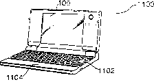
图4是包括本发明显示器件的便携式个人电脑的示意图;
图5是包括本发明显示器件的移动电话的示意图;
图6是包括本发明显示器件的数字照相机的示意图。
具体实施方式
英国专利申请0023787.5描述了一种包含有机电致发光有源阵列的显示器件,它包含可在一个帧周期内调整像素的通态工作周期以提供灰度调整的驱动电路。该显示器提供像素的接通时间的脉宽调制并且人眼的综合功能觉察到这一作为发射光强度的调制。接通时间的调制与常规的亮度控制完全相反以提供在这样的器件中的灰度调整,也就是供给电流的瞬态幅度的控制。图1是英国专利申请0023787.5所公开的像素级电路的电路图。
图1是在一有源阵列OELD显示屏内的一单独的像素10的电路图。该电路利用多晶硅TFT元件来实现,包括一个MOS输入比较器12以及两个选通门T1和T2。比较器12包括一个长尾差动对(long tail differential pair)16以及一个反相器18。使用选通门可避免所谓的“馈通”,即与其他电路电压的耦合。比较器12的反相输入端(+)连到一波形源VDRV。非反相输入端(-)连到一存储电容C1和选通门T1。选通门T1受波形VSCAN控制。比较器的输出端连到选通门T2。选通门T2控制流入有机发光元件14的电流。通过向VDRV施加一时变信号,根据施加到选通门T1的相对于电容C1和比较器12的另一端的数据电压VDAT的值,发光元件14被接通一段时间。
在行式驱动设计中,VSCAN将像素单元的选通门T1的状态设置在相同的行。当选通门T1关闭时,数据电压VDAT被传送到比较器12的反相输入端以及电容C1。随后,当选通门T1打开时,数据电压由电容C1存储。然后触发VDRV。当比较器12的反相输入端的电压V+小于比较器12的非反相输入端的电压V-时,比较器输出LO信号,该信号使发光元件14进入通态。当比较器12的反相输入端的电压V+大于比较器12的非反相输入端的电压V-时,比较器输出HI信号,该信号使发光元件14处于断路状态。由此生成的并由电容C1存储的数据电压将发光元件14保持的通态持续时间调整为一个帧周期。
帧周期一般为20mS并且由于发光元件14的响应时间为毫微秒级,多晶硅TFT的速度以及任何寄生电容变为驱动设计工作中的限制因素。也就是说,可以达到特别有效的转换。
在图1所示的电路中,公共工作电压VOELD被用于所有相同类型的OELD像素。电压VOELD有外部设置并且独立于驱动电路的供给电压VDD。这就大大地增加了控制用于OELD偏置条件的灵活性。
将给出适用于图1电路中的比较器12的详细原理的描述。
由于独立的比较器被提供给各个像素,所以应尽可能地保持电路面积最小以及比较器的能耗最低。此外,为了实现高数量的灰度级,比较器必须能识别输入电压的微小差异。例如,如果希望实现256灰度级而电压摆动为0V至5V,那么很显然ΔV=19.5Mv是最合适的。因此转换必须很快速,但是从先前的讨论中可知,最好应在所述电路的性能之内。
实现图1中的比较器12的的详细电路图在图2示出。图2的电路包括两个单元:一个CMOS差分放大器16,以及一个CMOS反相器18。CMOS反相器18快速地将选通门T2转到全开或全关。为了电平变换目的,反相器18的电源供给可以与差分单元16的不同。
差分单元16包括连接在VDD线与地之间的晶体管T3,T4和T6的漏级-源级串联连接电路,以及类似的晶体管T3,T5和T7连接电路,其中晶体管T5和T7与晶体管T4和T6并联连接。晶体管T4和T5的各自的栅极构成比较器12的两个输入端(+),(-),而晶体管T3的门接收偏置电压VBLAS。输出单元18包括两个晶体管T8和T9,它们是漏级-源级串联连接在VDD线与地之间的。比较器的输出端VOUT取自晶体管T8和T9之间的连接处,晶体管T8和T9的栅极接收自晶体管T4和T6之间的接合处。图2所示的电路使用了7个TFT。如果T1和T2分别使用TFT,每个像素的TFT总数达到9。如同所示出的,薄膜晶体管T1,T2,T3,T4,T5以及T8是p型的,薄膜晶体管T6,T7,以及T9是n型的。所有这些薄膜晶体管,以及存储电容器,OELD和所有连接引线必须被容纳于一个像素区域内。具体地,像素面积可为70.5μm2,OELD(在图3中标为“LEP”)可指定为直径为30μm的圆形区域。
如图3所示,电路元件被分配在15μm×15μm的矩形区域内。这比得上一可达到的10μm/μm的TFT大小(W/L)。一般地,各个电路面积最好是等于发光元件面积的四分之一。十个矩形电路区域的布置如图3所示。它们包括:一个电流源区域20,两个输入对区域22,两个电流镜电路区域24,两个电平移位器区域26,一个转换区域28以及一个存储电容器区域30。
按照本发明,可以确定最敏感地感知晶体管特性变化的器件元件。已经测定最敏感的感知元件是输入对(22)以及电流镜对(24)。输入对由晶体管T4和T5构成,电流镜对由晶体管T6和T7构成。本发明从某种程度上属于将两个电流镜电路区域24布置为互相毗邻以具有其矩形区域的一个公共边,将两个输入对电路区域22布置为互相毗邻以具有其矩形区域的一个公共边,并将所有的输入对电路区域布置为与相应的一个电流镜电路区域毗邻以各具有其矩形区域的一个公共边。即,这四个电路区域形成一个正方形,该正方形的一半被两个输入对晶体管占据,而另一半被两个电流镜晶体管占据。
最好是,两个电流镜电路区域互相毗邻以具有其矩形区域的一个公共边,两个输入对电路区域互相毗邻以具有其矩形区域的一个公共边,两个电平移位器电路区域互相毗邻以具有其矩形区域的一个公共边,所有输入对电路区域毗邻相应的一个电流镜电路区域,以及一个电流镜电路区域毗邻一个电平移位器电路区域以具有其矩形区域的一个公共边。最好是,电流源电路区域毗邻其中一个输入对电路区域以具有其矩形区域的一个公共边。最好是,电流源电路区域毗邻其中一个电平移位器电路区域以具有其矩形区域的一个公共边。最好是,电容器电路区域毗邻其中一个电流镜电路区域以具有其矩形区域的一个公共边。最好是,一个转换区域毗邻其中一个输入对电路区域以具有其矩形区域的一个公共边。最好是,所述的一个转换区域毗邻所述电容器电路区域以具有其矩形区域的一个公共边。最好是,第二个转换区域毗邻其中一个电流镜电路区域以具有其矩形区域的一个公共边。最好是,第二个转换区域毗邻其中一个电平移位器电路区域以具有其矩形区域的一个公共边。图3所示的这些优选方式,使得像素内的p型和n型掺杂区域保持在最小。
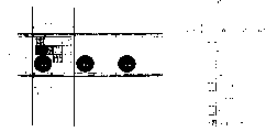
邻近的像素可布置为具有不同的波长输出的发光元件。因此,图3中的3个LEP元件可具有例如在光谱的红,绿,蓝区域中各自的输出。由此实现彩色显示。
尽管前面涉及到有源阵列OELD显示屏,但是本发明并不限于这样的显示屏。本发明可用于由多个按照本发明布置的电路区域的像素所构成的任何显示器件。同样地,尽管当本发明用于采用TFT技术制造的显示器件时能获得特别的益处,但是并不限于采用TFT技术实现的显示器件。本发明不仅可适用于薄膜晶体管技术,而且可适用于硅晶体管。可以使用几种不同的方式将硅晶体管放置在显示器衬底上。例如,可将硅晶体管放置在液态内。
本发明适用于小型的、便携式电子产品,例如移动电话,计算机,CD播放机,DVD播放机等等,本发明并不限于这些产品。
现在将说明几种使用上述有机电致发光显示器件的电子设备。
<1:便携式计机>
将描述采用按照上述一个实施例的显示器的便携式个人计算机的例子。
图4是表示个人计算机结构的等角视图。图中,个人计算机1100具有包括键盘1102及显示单元1106的机身1104。显示单元1106使用按照如上所述的本发明制造的显示屏来实现。
<2:移动电话>
下面,将描述将显示器用于移动电话的显示部分的例子。图5是表示移动电话结构的等角视图。图中,移动电话1200具有多个操作键1202,一个听筒1204,一个话筒1206,以及一个显示屏100。显示屏100使用按照如上所述的本发明制造的显示屏来实现。
<3:数字静态照相机>
下面,将描述使用OEL显示器作取景器的数字静态照相机。图6是表示数字静态照相机结构以及与外部主要装置的连接的等角视图。
普通的照相机根据物体的光学图像在胶片上感光,而数字静态照相机1300通过使用例如,电荷耦合器件(CCD)的光电转换来产生来自物体的光学图像的成像信号。数字静态照相机1300具有一个位于壳体1302的背面的OEL元件100以根据来自CCD的成像信号执行显像。因此,显示屏100用作用于显像物体的取景器。含有光学镜头的照片接收单元1304以及CCD位于壳体1302的前部(图中在后)。
当摄影师确定显像在OEL元件板100上的物体图像并释放快门时,来自CCD的成像信号被传送并存储到电路板1308内的存储器中。在数字静态照相机1300中,用于数据传输的视频信号输出端1312以及输入/输出端1314设置在壳体1302的一侧。如图中所示,如果需要,电视监视器1430以及个人计算机1440可以分别接到视频信号输出端1312以及输入/输出端1314。存储在电路板1308的存储器内的成像信号通过给定的操作可以输出到电视监视器1430以及个人计算机1440。
除了图4所示的个人计算机,图5所示的移动电话,以及图6所示的数字静态照相机外,电子装置的例子还包括电视机,探视器型和监控型视频磁带录像机,汽车导航系统,寻呼机,电子笔记本,便携式计算器,文字处理器,工作站,电视电话机,销售点系统(POS)终端,以及具有触摸屏的设备。当然,本发明的上述实施例可以应用到这些电子设备的显示部件上。
Claims (12)
1.一种显示器件,包括多个像素,每个像素含有一个发光元件以及多个矩形的电路区域,所述电路区域包括:一个电流源电路区域,两个电平移位器电路区域,一个转换电路区域,一个电容器电路区域,两个电流镜电路区域,和两个输入对电路区域,其中
所述两个电流镜电路区域互相毗邻以具有其矩形区域的一个公共边;
所述两个输入对电路区域互相毗邻以具有其矩形区域的一个公共边;
所有输入对电路区域毗邻相应的一个电流镜电路区域以使每一个具有其矩形区域的一个公共边;所述两个电平移位器电路区域互相毗邻以具有其矩形区域的一个公共边,并且一个电流镜电路区域毗邻一个电平移位器电路区域以具有其矩形区域的一个公共边;
所述转换电路区域毗邻输入对电路区域中的一个以具有其矩形区域的一个公共边;以及
所述电容器电路区域毗邻电流镜电路区域中的一个以具有其矩形区域的一个公共边。
2.如权利要求1所述的显示器件,其特征是,所述电流源电路区域毗邻输入对电路区域中的一个以具有其矩形区域的一个公共边。
3.如权利要求1所述的显示器件,其特征是,所述电流源电路区域毗邻所述电平移位器电路区域中的一个以具有其矩形区域的一个公共边。
4.如权利要求1所述的显示器件,其特征是,所述转换电路区域毗邻所述电容器电路区域以具有其矩形区域的一个公共边。
5.如权利要求1所述的显示器件,其特征是,所述多个电路区域的每一个包括一个第二转换电路区域。
6.如权利要求5所述的显示器件,其特征是,所述第二转换电路区域毗邻所述电流镜电路区域中的一个以具有其矩形区域的一个公共边。
7.如权利要求5所述的显示器件,其特征是,所述第二转换电路区域毗邻所述电平移位器电路区域中的一个以具有其矩形区域的一个公共边。
8.如权利要求1所述的显示器件,其特征是,所述多个电路区域的每一个具有相同的大小。
9.如权利要求1所述的显示器件,其特征是,各个像素为矩形,并且各个发光元件位于各自的像素的一角内。
10.如权利要求1所述的显示器件,其特征是,所述多个电路区域的每一个的面积等于所述发光元件面积的1/π。
11.如权利要求1所述的显示器件,其特征是,所述多个电路区域的一个或多个包括薄膜晶体管。
12.如权利要求1所述的显示器件,其特征是,所述发光元件是有机电致发光元件。
Applications Claiming Priority (2)
| Application Number | Priority Date | Filing Date | Title |
|---|---|---|---|
| GB0023789A GB2367414A (en) | 2000-09-28 | 2000-09-28 | Display device using TFT's |
| GB0023789.1 | 2000-09-28 |
Publications (2)
| Publication Number | Publication Date |
|---|---|
| CN1346121A CN1346121A (zh) | 2002-04-24 |
| CN1248186C true CN1248186C (zh) | 2006-03-29 |
Family
ID=9900305
Family Applications (1)
| Application Number | Title | Priority Date | Filing Date |
|---|---|---|---|
| CNB011372427A Expired - Fee Related CN1248186C (zh) | 2000-09-28 | 2001-09-28 | 显示器件 |
Country Status (4)
| Country | Link |
|---|---|
| US (1) | US7002536B2 (zh) |
| JP (1) | JP2002189446A (zh) |
| CN (1) | CN1248186C (zh) |
| GB (2) | GB2367414A (zh) |
Families Citing this family (18)
| Publication number | Priority date | Publication date | Assignee | Title |
|---|---|---|---|---|
| GB2367413A (en) * | 2000-09-28 | 2002-04-03 | Seiko Epson Corp | Organic electroluminescent display device |
| JP3899886B2 (ja) | 2001-10-10 | 2007-03-28 | 株式会社日立製作所 | 画像表示装置 |
| JP3859483B2 (ja) * | 2001-10-26 | 2006-12-20 | 沖電気工業株式会社 | 駆動回路 |
| SG110023A1 (en) * | 2002-03-01 | 2005-04-28 | Semiconductor Energy Lab | Display device, light emitting device, and electronic eqipment |
| JP2005536771A (ja) * | 2002-08-21 | 2005-12-02 | コーニンクレッカ フィリップス エレクトロニクス エヌ ヴィ | 表示装置 |
| CN100440291C (zh) * | 2002-09-23 | 2008-12-03 | 皇家飞利浦电子股份有限公司 | 带有光敏单元的矩阵显示器件 |
| GB0224277D0 (en) * | 2002-10-18 | 2002-11-27 | Koninkl Philips Electronics Nv | Electroluminescent display devices |
| JP4350370B2 (ja) * | 2002-12-27 | 2009-10-21 | 株式会社半導体エネルギー研究所 | 電子回路及び電子機器 |
| US7333099B2 (en) * | 2003-01-06 | 2008-02-19 | Semiconductor Energy Laboratory Co., Ltd. | Electronic circuit, display device, and electronic apparatus |
| FR2857146A1 (fr) * | 2003-07-03 | 2005-01-07 | Thomson Licensing Sa | Dispositif d'affichage d'images a matrice active |
| JP4501785B2 (ja) * | 2004-09-30 | 2010-07-14 | セイコーエプソン株式会社 | 画素回路及び電子機器 |
| CN101840455B (zh) * | 2010-04-23 | 2012-01-25 | 汕头超声显示器(二厂)有限公司 | 一种tft有源阵列周边电路的设计方法 |
| JP6157178B2 (ja) | 2013-04-01 | 2017-07-05 | ソニーセミコンダクタソリューションズ株式会社 | 表示装置 |
| CN110796985B (zh) * | 2018-07-24 | 2022-03-11 | 群创光电股份有限公司 | 电子装置 |
| US10885830B2 (en) * | 2018-07-24 | 2021-01-05 | Innolux Corporation | Electronic device capable of reducing color shift |
| US11710445B2 (en) | 2019-01-24 | 2023-07-25 | Google Llc | Backplane configurations and operations |
| CN111489687B (zh) * | 2020-04-24 | 2021-08-06 | 厦门天马微电子有限公司 | 一种像素驱动电路、显示面板、显示装置以及驱动方法 |
| CN113948040B (zh) * | 2021-11-22 | 2023-07-07 | 视涯科技股份有限公司 | 显示面板 |
Family Cites Families (12)
| Publication number | Priority date | Publication date | Assignee | Title |
|---|---|---|---|---|
| US4528480A (en) * | 1981-12-28 | 1985-07-09 | Nippon Telegraph & Telephone | AC Drive type electroluminescent display device |
| US5734297A (en) * | 1996-03-29 | 1998-03-31 | Philips Electronics North America Corporation | Rail-to-rail input stages with constant gm and constant common-mode output currents |
| US5903246A (en) * | 1997-04-04 | 1999-05-11 | Sarnoff Corporation | Circuit and method for driving an organic light emitting diode (O-LED) display |
| US6054874A (en) * | 1997-07-02 | 2000-04-25 | Cypress Semiconductor Corp. | Output driver circuit with switched current source |
| JP3552500B2 (ja) * | 1997-11-12 | 2004-08-11 | セイコーエプソン株式会社 | 論理振幅レベル変換回路,液晶装置及び電子機器 |
| GB9812739D0 (en) * | 1998-06-12 | 1998-08-12 | Koninkl Philips Electronics Nv | Active matrix electroluminescent display devices |
| JP3858486B2 (ja) * | 1998-11-26 | 2006-12-13 | セイコーエプソン株式会社 | シフトレジスタ回路、電気光学装置および電子機器 |
| US6744299B2 (en) * | 1999-01-06 | 2004-06-01 | Victorian Systems, Inc. | Electronic array having nodes and methods |
| GB2349996A (en) * | 1999-05-12 | 2000-11-15 | Sharp Kk | Voltage level converter for an active matrix LCD |
| TW518642B (en) * | 2000-06-27 | 2003-01-21 | Semiconductor Energy Lab | Level shifter |
| US6566970B2 (en) * | 2001-02-02 | 2003-05-20 | Broadcom Corporation | High-speed, high PSRR, wide operating range voltage controlled oscillator |
| JP4103468B2 (ja) * | 2002-06-28 | 2008-06-18 | 日本電気株式会社 | 差動回路と増幅回路及び該増幅回路を用いた表示装置 |
-
2000
- 2000-09-28 GB GB0023789A patent/GB2367414A/en not_active Withdrawn
-
2001
- 2001-09-26 US US09/962,586 patent/US7002536B2/en not_active Expired - Fee Related
- 2001-09-27 GB GB0123272A patent/GB2370906B/en not_active Expired - Fee Related
- 2001-09-27 JP JP2001296484A patent/JP2002189446A/ja active Pending
- 2001-09-28 CN CNB011372427A patent/CN1248186C/zh not_active Expired - Fee Related
Also Published As
| Publication number | Publication date |
|---|---|
| JP2002189446A (ja) | 2002-07-05 |
| US7002536B2 (en) | 2006-02-21 |
| GB0123272D0 (en) | 2001-11-21 |
| GB2370906A (en) | 2002-07-10 |
| GB2367414A (en) | 2002-04-03 |
| US20020047817A1 (en) | 2002-04-25 |
| CN1346121A (zh) | 2002-04-24 |
| GB0023789D0 (en) | 2000-11-08 |
| GB2370906B (en) | 2002-12-18 |
Similar Documents
| Publication | Publication Date | Title |
|---|---|---|
| CN1248186C (zh) | 显示器件 | |
| US10818226B2 (en) | Pixel circuit, method for driving the same, and display apparatus | |
| US11961477B2 (en) | Pixel driving circuit, and display panel and driving method thereof | |
| US11328670B2 (en) | Pixel circuit, driving method thereof, and display apparatus | |
| CN107342044B (zh) | 像素电路、显示面板和像素电路的驱动方法 | |
| US7187355B2 (en) | Display device, method of driving a display device, electronic apparatus | |
| KR100997977B1 (ko) | 광센서 및 이를 이용한 표시 장치 | |
| US11741909B2 (en) | Pixel circuit and driving method therefor, and display substrate and display device | |
| WO2019214286A1 (zh) | 像素电路和电致发光显示面板、其驱动方法及显示装置 | |
| US10657888B2 (en) | Driving method for pixel driving circuit, display panel and display device | |
| US11156868B2 (en) | Charge release circuit and driving method therefor, and display device | |
| US11348517B2 (en) | Pixel circuit, driving method thereof and display device | |
| KR20030063188A (ko) | 전기 회로 | |
| US11367393B2 (en) | Display panel, driving method thereof and display device | |
| TWI408658B (zh) | 畫素電路、具有畫素電路的顯示裝置以及操作畫素電路的方法 | |
| US10553159B2 (en) | Pixel circuit, display panel and display device | |
| KR20020032571A (ko) | 문턱 전압 변동을 상쇄하는 상보형 구동 트랜지스터를구비한 유기 전계 발광 디스플레이 등의 전류 구동 전기광학 장치 | |
| CN111383598A (zh) | 像素补偿电路及其控制方法、显示驱动装置、显示设备 | |
| US11074860B2 (en) | Optical signal noise reduction circuit, optical signal noise reduction method and display panel | |
| CN115101022A (zh) | 一种像素驱动电路、显示面板及显示装置 | |
| CN112086069B (zh) | 分区显示结构、显示面板、有机发光二极管显示面板 | |
| US7292210B2 (en) | Circuit for driving flat panel display | |
| US11735111B1 (en) | Driving circuit, driving method and display panel | |
| US20240169892A1 (en) | Driving circuit, display panel, and driving method thereof | |
| US20050140304A1 (en) | Organic electroluminescent device and driving circuit thereof |
Legal Events
| Date | Code | Title | Description |
|---|---|---|---|
| C06 | Publication | ||
| PB01 | Publication | ||
| C10 | Entry into substantive examination | ||
| SE01 | Entry into force of request for substantive examination | ||
| C14 | Grant of patent or utility model | ||
| GR01 | Patent grant | ||
| CF01 | Termination of patent right due to non-payment of annual fee |
Granted publication date: 20060329 Termination date: 20150928 |
|
| EXPY | Termination of patent right or utility model |