CN1246504C - Apparatus and method for electrolytically depositing copper on semiconductor workpiece - Google Patents
Apparatus and method for electrolytically depositing copper on semiconductor workpiece Download PDFInfo
- Publication number
- CN1246504C CN1246504C CNB998041289A CN99804128A CN1246504C CN 1246504 C CN1246504 C CN 1246504C CN B998041289 A CNB998041289 A CN B998041289A CN 99804128 A CN99804128 A CN 99804128A CN 1246504 C CN1246504 C CN 1246504C
- Authority
- CN
- China
- Prior art keywords
- layer
- copper
- workpiece
- metal
- complexing agent
- Prior art date
- Legal status (The legal status is an assumption and is not a legal conclusion. Google has not performed a legal analysis and makes no representation as to the accuracy of the status listed.)
- Expired - Fee Related
Links
- 229910052802 copper Inorganic materials 0.000 title claims abstract description 147
- 239000010949 copper Substances 0.000 title claims abstract description 147
- RYGMFSIKBFXOCR-UHFFFAOYSA-N Copper Chemical compound [Cu] RYGMFSIKBFXOCR-UHFFFAOYSA-N 0.000 title claims abstract description 145
- 238000000034 method Methods 0.000 title claims abstract description 80
- 238000000151 deposition Methods 0.000 title claims description 35
- 239000004065 semiconductor Substances 0.000 title description 27
- 230000004888 barrier function Effects 0.000 claims abstract description 14
- 238000001465 metallisation Methods 0.000 claims abstract description 3
- 238000007747 plating Methods 0.000 claims description 100
- KRKNYBCHXYNGOX-UHFFFAOYSA-N citric acid Chemical compound OC(=O)CC(O)(C(O)=O)CC(O)=O KRKNYBCHXYNGOX-UHFFFAOYSA-N 0.000 claims description 73
- 229910052751 metal Inorganic materials 0.000 claims description 68
- 239000002184 metal Substances 0.000 claims description 68
- 239000008139 complexing agent Substances 0.000 claims description 44
- KCXVZYZYPLLWCC-UHFFFAOYSA-N EDTA Chemical compound OC(=O)CN(CC(O)=O)CCN(CC(O)=O)CC(O)=O KCXVZYZYPLLWCC-UHFFFAOYSA-N 0.000 claims description 30
- 230000000903 blocking effect Effects 0.000 claims description 30
- 238000009713 electroplating Methods 0.000 claims description 26
- 238000005240 physical vapour deposition Methods 0.000 claims description 21
- 238000005728 strengthening Methods 0.000 claims description 21
- 230000008021 deposition Effects 0.000 claims description 19
- 238000005516 engineering process Methods 0.000 claims description 18
- 239000002253 acid Substances 0.000 claims description 17
- 238000011049 filling Methods 0.000 claims description 15
- 230000008569 process Effects 0.000 claims description 14
- 230000002787 reinforcement Effects 0.000 claims description 14
- 229910000365 copper sulfate Inorganic materials 0.000 claims description 12
- ARUVKPQLZAKDPS-UHFFFAOYSA-L copper(II) sulfate Chemical compound [Cu+2].[O-][S+2]([O-])([O-])[O-] ARUVKPQLZAKDPS-UHFFFAOYSA-L 0.000 claims description 12
- 239000007788 liquid Substances 0.000 claims description 12
- 239000003513 alkali Substances 0.000 claims description 11
- 239000000758 substrate Substances 0.000 claims description 11
- 239000000428 dust Substances 0.000 claims description 10
- 239000003792 electrolyte Substances 0.000 claims description 10
- 230000005518 electrochemistry Effects 0.000 claims description 8
- JPVYNHNXODAKFH-UHFFFAOYSA-N Cu2+ Chemical compound [Cu+2] JPVYNHNXODAKFH-UHFFFAOYSA-N 0.000 claims description 7
- 150000001735 carboxylic acids Chemical class 0.000 claims description 6
- 150000003839 salts Chemical class 0.000 claims description 5
- 238000004062 sedimentation Methods 0.000 claims description 4
- 150000002739 metals Chemical class 0.000 claims description 3
- 230000015572 biosynthetic process Effects 0.000 claims description 2
- 230000000536 complexating effect Effects 0.000 claims description 2
- 238000007670 refining Methods 0.000 claims description 2
- 238000005406 washing Methods 0.000 claims 3
- 229910021645 metal ion Inorganic materials 0.000 claims 2
- 229910000906 Bronze Inorganic materials 0.000 claims 1
- 239000010974 bronze Substances 0.000 claims 1
- 238000010668 complexation reaction Methods 0.000 claims 1
- KUNSUQLRTQLHQQ-UHFFFAOYSA-N copper tin Chemical compound [Cu].[Sn] KUNSUQLRTQLHQQ-UHFFFAOYSA-N 0.000 claims 1
- 210000000438 stratum basale Anatomy 0.000 claims 1
- 238000005019 vapor deposition process Methods 0.000 claims 1
- 239000011248 coating agent Substances 0.000 abstract description 32
- 238000000576 coating method Methods 0.000 abstract description 32
- 239000000463 material Substances 0.000 abstract description 19
- 238000004070 electrodeposition Methods 0.000 abstract description 12
- 238000005137 deposition process Methods 0.000 abstract 1
- 235000012431 wafers Nutrition 0.000 description 24
- 235000015165 citric acid Nutrition 0.000 description 18
- BFNBIHQBYMNNAN-UHFFFAOYSA-N ammonium sulfate Chemical compound N.N.OS(O)(=O)=O BFNBIHQBYMNNAN-UHFFFAOYSA-N 0.000 description 13
- 229910052921 ammonium sulfate Inorganic materials 0.000 description 13
- 235000011130 ammonium sulphate Nutrition 0.000 description 13
- 239000000243 solution Substances 0.000 description 13
- LYCAIKOWRPUZTN-UHFFFAOYSA-N Ethylene glycol Chemical compound OCCO LYCAIKOWRPUZTN-UHFFFAOYSA-N 0.000 description 11
- 239000011810 insulating material Substances 0.000 description 9
- QPLDLSVMHZLSFG-UHFFFAOYSA-N Copper oxide Chemical compound [Cu]=O QPLDLSVMHZLSFG-UHFFFAOYSA-N 0.000 description 8
- KGBXLFKZBHKPEV-UHFFFAOYSA-N boric acid Chemical compound OB(O)O KGBXLFKZBHKPEV-UHFFFAOYSA-N 0.000 description 8
- 241000196324 Embryophyta Species 0.000 description 7
- 239000004327 boric acid Substances 0.000 description 7
- 238000005229 chemical vapour deposition Methods 0.000 description 7
- 238000012546 transfer Methods 0.000 description 7
- 238000004519 manufacturing process Methods 0.000 description 6
- 239000000203 mixture Substances 0.000 description 6
- 150000001875 compounds Chemical class 0.000 description 5
- 230000000875 corresponding effect Effects 0.000 description 5
- 229960004643 cupric oxide Drugs 0.000 description 5
- XLYOFNOQVPJJNP-UHFFFAOYSA-N water Substances O XLYOFNOQVPJJNP-UHFFFAOYSA-N 0.000 description 5
- 229910000838 Al alloy Inorganic materials 0.000 description 4
- PXHVJJICTQNCMI-UHFFFAOYSA-N Nickel Chemical compound [Ni] PXHVJJICTQNCMI-UHFFFAOYSA-N 0.000 description 4
- VYPSYNLAJGMNEJ-UHFFFAOYSA-N Silicium dioxide Chemical compound O=[Si]=O VYPSYNLAJGMNEJ-UHFFFAOYSA-N 0.000 description 4
- 150000001412 amines Chemical class 0.000 description 4
- 238000000137 annealing Methods 0.000 description 4
- 230000008901 benefit Effects 0.000 description 4
- 238000006243 chemical reaction Methods 0.000 description 4
- 239000004020 conductor Substances 0.000 description 4
- 239000008367 deionised water Substances 0.000 description 4
- 229910021641 deionized water Inorganic materials 0.000 description 4
- 238000010586 diagram Methods 0.000 description 4
- 239000006259 organic additive Substances 0.000 description 4
- XUIMIQQOPSSXEZ-UHFFFAOYSA-N Silicon Chemical compound [Si] XUIMIQQOPSSXEZ-UHFFFAOYSA-N 0.000 description 3
- HEMHJVSKTPXQMS-UHFFFAOYSA-M Sodium hydroxide Chemical compound [OH-].[Na+] HEMHJVSKTPXQMS-UHFFFAOYSA-M 0.000 description 3
- 125000003277 amino group Chemical group 0.000 description 3
- 238000005868 electrolysis reaction Methods 0.000 description 3
- 238000004377 microelectronic Methods 0.000 description 3
- 238000012545 processing Methods 0.000 description 3
- 238000004626 scanning electron microscopy Methods 0.000 description 3
- 239000010703 silicon Substances 0.000 description 3
- 229910052710 silicon Inorganic materials 0.000 description 3
- -1 tantalum nitrides Chemical class 0.000 description 3
- 238000013519 translation Methods 0.000 description 3
- QGZKDVFQNNGYKY-UHFFFAOYSA-O Ammonium Chemical compound [NH4+] QGZKDVFQNNGYKY-UHFFFAOYSA-O 0.000 description 2
- VHUUQVKOLVNVRT-UHFFFAOYSA-N Ammonium hydroxide Chemical compound [NH4+].[OH-] VHUUQVKOLVNVRT-UHFFFAOYSA-N 0.000 description 2
- 239000005751 Copper oxide Substances 0.000 description 2
- XEEYBQQBJWHFJM-UHFFFAOYSA-N Iron Chemical compound [Fe] XEEYBQQBJWHFJM-UHFFFAOYSA-N 0.000 description 2
- NINIDFKCEFEMDL-UHFFFAOYSA-N Sulfur Chemical compound [S] NINIDFKCEFEMDL-UHFFFAOYSA-N 0.000 description 2
- NRTOMJZYCJJWKI-UHFFFAOYSA-N Titanium nitride Chemical group [Ti]#N NRTOMJZYCJJWKI-UHFFFAOYSA-N 0.000 description 2
- 239000000908 ammonium hydroxide Substances 0.000 description 2
- QVGXLLKOCUKJST-UHFFFAOYSA-N atomic oxygen Chemical compound [O] QVGXLLKOCUKJST-UHFFFAOYSA-N 0.000 description 2
- 239000002585 base Substances 0.000 description 2
- 230000008859 change Effects 0.000 description 2
- 239000003795 chemical substances by application Substances 0.000 description 2
- 239000002131 composite material Substances 0.000 description 2
- 150000001879 copper Chemical class 0.000 description 2
- 229910000431 copper oxide Inorganic materials 0.000 description 2
- 230000002950 deficient Effects 0.000 description 2
- 238000009792 diffusion process Methods 0.000 description 2
- 230000000694 effects Effects 0.000 description 2
- 230000005611 electricity Effects 0.000 description 2
- 239000007789 gas Substances 0.000 description 2
- 238000009413 insulation Methods 0.000 description 2
- 229910052759 nickel Inorganic materials 0.000 description 2
- 229910052760 oxygen Inorganic materials 0.000 description 2
- 239000001301 oxygen Substances 0.000 description 2
- 239000002245 particle Substances 0.000 description 2
- 238000001259 photo etching Methods 0.000 description 2
- 230000009467 reduction Effects 0.000 description 2
- 238000007789 sealing Methods 0.000 description 2
- 229910052814 silicon oxide Inorganic materials 0.000 description 2
- 229910052717 sulfur Inorganic materials 0.000 description 2
- 239000011593 sulfur Substances 0.000 description 2
- WGTYBPLFGIVFAS-UHFFFAOYSA-M tetramethylammonium hydroxide Chemical compound [OH-].C[N+](C)(C)C WGTYBPLFGIVFAS-UHFFFAOYSA-M 0.000 description 2
- 238000007740 vapor deposition Methods 0.000 description 2
- 230000000007 visual effect Effects 0.000 description 2
- 239000011800 void material Substances 0.000 description 2
- 241000370738 Chlorion Species 0.000 description 1
- 239000005749 Copper compound Substances 0.000 description 1
- JJLJMEJHUUYSSY-UHFFFAOYSA-L Copper hydroxide Chemical compound [OH-].[OH-].[Cu+2] JJLJMEJHUUYSSY-UHFFFAOYSA-L 0.000 description 1
- 239000005750 Copper hydroxide Substances 0.000 description 1
- 229910000881 Cu alloy Inorganic materials 0.000 description 1
- 240000004859 Gamochaeta purpurea Species 0.000 description 1
- 229910000990 Ni alloy Inorganic materials 0.000 description 1
- 229910000831 Steel Inorganic materials 0.000 description 1
- NSOXQYCFHDMMGV-UHFFFAOYSA-N Tetrakis(2-hydroxypropyl)ethylenediamine Chemical compound CC(O)CN(CC(C)O)CCN(CC(C)O)CC(C)O NSOXQYCFHDMMGV-UHFFFAOYSA-N 0.000 description 1
- HCHKCACWOHOZIP-UHFFFAOYSA-N Zinc Chemical compound [Zn] HCHKCACWOHOZIP-UHFFFAOYSA-N 0.000 description 1
- 229910001297 Zn alloy Inorganic materials 0.000 description 1
- 239000000654 additive Substances 0.000 description 1
- 230000000996 additive effect Effects 0.000 description 1
- 239000000853 adhesive Substances 0.000 description 1
- 230000001070 adhesive effect Effects 0.000 description 1
- 229910045601 alloy Inorganic materials 0.000 description 1
- 239000000956 alloy Substances 0.000 description 1
- 239000004411 aluminium Substances 0.000 description 1
- 229910052782 aluminium Inorganic materials 0.000 description 1
- XAGFODPZIPBFFR-UHFFFAOYSA-N aluminium Chemical compound [Al] XAGFODPZIPBFFR-UHFFFAOYSA-N 0.000 description 1
- 239000012298 atmosphere Substances 0.000 description 1
- 238000005282 brightening Methods 0.000 description 1
- 239000000919 ceramic Substances 0.000 description 1
- 238000004140 cleaning Methods 0.000 description 1
- 239000010941 cobalt Substances 0.000 description 1
- 229910017052 cobalt Inorganic materials 0.000 description 1
- GUTLYIVDDKVIGB-UHFFFAOYSA-N cobalt atom Chemical compound [Co] GUTLYIVDDKVIGB-UHFFFAOYSA-N 0.000 description 1
- RIVZIMVWRDTIOQ-UHFFFAOYSA-N cobalt iron Chemical compound [Fe].[Co].[Co].[Co] RIVZIMVWRDTIOQ-UHFFFAOYSA-N 0.000 description 1
- 238000010276 construction Methods 0.000 description 1
- 150000001880 copper compounds Chemical class 0.000 description 1
- 229910001956 copper hydroxide Inorganic materials 0.000 description 1
- 229910001431 copper ion Inorganic materials 0.000 description 1
- TVZPLCNGKSPOJA-UHFFFAOYSA-N copper zinc Chemical compound [Cu].[Zn] TVZPLCNGKSPOJA-UHFFFAOYSA-N 0.000 description 1
- 230000002596 correlated effect Effects 0.000 description 1
- 238000005260 corrosion Methods 0.000 description 1
- 230000007797 corrosion Effects 0.000 description 1
- 230000001934 delay Effects 0.000 description 1
- 238000009826 distribution Methods 0.000 description 1
- 238000001035 drying Methods 0.000 description 1
- 239000008151 electrolyte solution Substances 0.000 description 1
- 230000002349 favourable effect Effects 0.000 description 1
- 238000011010 flushing procedure Methods 0.000 description 1
- 238000009499 grossing Methods 0.000 description 1
- 239000001257 hydrogen Substances 0.000 description 1
- 229910052739 hydrogen Inorganic materials 0.000 description 1
- WGCNASOHLSPBMP-UHFFFAOYSA-N hydroxyacetaldehyde Natural products OCC=O WGCNASOHLSPBMP-UHFFFAOYSA-N 0.000 description 1
- 239000004615 ingredient Substances 0.000 description 1
- 239000012774 insulation material Substances 0.000 description 1
- 229910052742 iron Inorganic materials 0.000 description 1
- 238000005304 joining Methods 0.000 description 1
- 230000005012 migration Effects 0.000 description 1
- 238000013508 migration Methods 0.000 description 1
- 230000003647 oxidation Effects 0.000 description 1
- 238000007254 oxidation reaction Methods 0.000 description 1
- 229910001950 potassium oxide Inorganic materials 0.000 description 1
- 230000001376 precipitating effect Effects 0.000 description 1
- 238000001556 precipitation Methods 0.000 description 1
- 238000003825 pressing Methods 0.000 description 1
- 239000000700 radioactive tracer Substances 0.000 description 1
- 230000000306 recurrent effect Effects 0.000 description 1
- 230000001105 regulatory effect Effects 0.000 description 1
- 229920006395 saturated elastomer Polymers 0.000 description 1
- 239000000377 silicon dioxide Substances 0.000 description 1
- 229960001866 silicon dioxide Drugs 0.000 description 1
- 235000012239 silicon dioxide Nutrition 0.000 description 1
- 239000010959 steel Substances 0.000 description 1
- 239000000126 substance Substances 0.000 description 1
- 229910052715 tantalum Inorganic materials 0.000 description 1
- MZLGASXMSKOWSE-UHFFFAOYSA-N tantalum nitride Chemical compound [Ta]#N MZLGASXMSKOWSE-UHFFFAOYSA-N 0.000 description 1
- 235000012976 tarts Nutrition 0.000 description 1
- 238000001149 thermolysis Methods 0.000 description 1
- 239000012745 toughening agent Substances 0.000 description 1
- 239000000080 wetting agent Substances 0.000 description 1
- 229910052725 zinc Inorganic materials 0.000 description 1
- 239000011701 zinc Substances 0.000 description 1
Images


Classifications
-
- H—ELECTRICITY
- H01—ELECTRIC ELEMENTS
- H01L—SEMICONDUCTOR DEVICES NOT COVERED BY CLASS H10
- H01L21/00—Processes or apparatus adapted for the manufacture or treatment of semiconductor or solid state devices or of parts thereof
- H01L21/02—Manufacture or treatment of semiconductor devices or of parts thereof
- H01L21/04—Manufacture or treatment of semiconductor devices or of parts thereof the devices having at least one potential-jump barrier or surface barrier, e.g. PN junction, depletion layer or carrier concentration layer
- H01L21/18—Manufacture or treatment of semiconductor devices or of parts thereof the devices having at least one potential-jump barrier or surface barrier, e.g. PN junction, depletion layer or carrier concentration layer the devices having semiconductor bodies comprising elements of Group IV of the Periodic System or AIIIBV compounds with or without impurities, e.g. doping materials
- H01L21/20—Deposition of semiconductor materials on a substrate, e.g. epitaxial growth solid phase epitaxy
-
- C—CHEMISTRY; METALLURGY
- C25—ELECTROLYTIC OR ELECTROPHORETIC PROCESSES; APPARATUS THEREFOR
- C25D—PROCESSES FOR THE ELECTROLYTIC OR ELECTROPHORETIC PRODUCTION OF COATINGS; ELECTROFORMING; APPARATUS THEREFOR
- C25D7/00—Electroplating characterised by the article coated
- C25D7/12—Semiconductors
- C25D7/123—Semiconductors first coated with a seed layer or a conductive layer
-
- C—CHEMISTRY; METALLURGY
- C23—COATING METALLIC MATERIAL; COATING MATERIAL WITH METALLIC MATERIAL; CHEMICAL SURFACE TREATMENT; DIFFUSION TREATMENT OF METALLIC MATERIAL; COATING BY VACUUM EVAPORATION, BY SPUTTERING, BY ION IMPLANTATION OR BY CHEMICAL VAPOUR DEPOSITION, IN GENERAL; INHIBITING CORROSION OF METALLIC MATERIAL OR INCRUSTATION IN GENERAL
- C23C—COATING METALLIC MATERIAL; COATING MATERIAL WITH METALLIC MATERIAL; SURFACE TREATMENT OF METALLIC MATERIAL BY DIFFUSION INTO THE SURFACE, BY CHEMICAL CONVERSION OR SUBSTITUTION; COATING BY VACUUM EVAPORATION, BY SPUTTERING, BY ION IMPLANTATION OR BY CHEMICAL VAPOUR DEPOSITION, IN GENERAL
- C23C28/00—Coating for obtaining at least two superposed coatings either by methods not provided for in a single one of groups C23C2/00 - C23C26/00 or by combinations of methods provided for in subclasses C23C and C25C or C25D
- C23C28/30—Coatings combining at least one metallic layer and at least one inorganic non-metallic layer
- C23C28/32—Coatings combining at least one metallic layer and at least one inorganic non-metallic layer including at least one pure metallic layer
- C23C28/322—Coatings combining at least one metallic layer and at least one inorganic non-metallic layer including at least one pure metallic layer only coatings of metal elements only
-
- C—CHEMISTRY; METALLURGY
- C23—COATING METALLIC MATERIAL; COATING MATERIAL WITH METALLIC MATERIAL; CHEMICAL SURFACE TREATMENT; DIFFUSION TREATMENT OF METALLIC MATERIAL; COATING BY VACUUM EVAPORATION, BY SPUTTERING, BY ION IMPLANTATION OR BY CHEMICAL VAPOUR DEPOSITION, IN GENERAL; INHIBITING CORROSION OF METALLIC MATERIAL OR INCRUSTATION IN GENERAL
- C23C—COATING METALLIC MATERIAL; COATING MATERIAL WITH METALLIC MATERIAL; SURFACE TREATMENT OF METALLIC MATERIAL BY DIFFUSION INTO THE SURFACE, BY CHEMICAL CONVERSION OR SUBSTITUTION; COATING BY VACUUM EVAPORATION, BY SPUTTERING, BY ION IMPLANTATION OR BY CHEMICAL VAPOUR DEPOSITION, IN GENERAL
- C23C28/00—Coating for obtaining at least two superposed coatings either by methods not provided for in a single one of groups C23C2/00 - C23C26/00 or by combinations of methods provided for in subclasses C23C and C25C or C25D
- C23C28/30—Coatings combining at least one metallic layer and at least one inorganic non-metallic layer
- C23C28/34—Coatings combining at least one metallic layer and at least one inorganic non-metallic layer including at least one inorganic non-metallic material layer, e.g. metal carbide, nitride, boride, silicide layer and their mixtures, enamels, phosphates and sulphates
-
- C—CHEMISTRY; METALLURGY
- C25—ELECTROLYTIC OR ELECTROPHORETIC PROCESSES; APPARATUS THEREFOR
- C25D—PROCESSES FOR THE ELECTROLYTIC OR ELECTROPHORETIC PRODUCTION OF COATINGS; ELECTROFORMING; APPARATUS THEREFOR
- C25D3/00—Electroplating: Baths therefor
- C25D3/02—Electroplating: Baths therefor from solutions
- C25D3/38—Electroplating: Baths therefor from solutions of copper
-
- C—CHEMISTRY; METALLURGY
- C25—ELECTROLYTIC OR ELECTROPHORETIC PROCESSES; APPARATUS THEREFOR
- C25D—PROCESSES FOR THE ELECTROLYTIC OR ELECTROPHORETIC PRODUCTION OF COATINGS; ELECTROFORMING; APPARATUS THEREFOR
- C25D5/00—Electroplating characterised by the process; Pretreatment or after-treatment of workpieces
- C25D5/10—Electroplating with more than one layer of the same or of different metals
-
- C—CHEMISTRY; METALLURGY
- C25—ELECTROLYTIC OR ELECTROPHORETIC PROCESSES; APPARATUS THEREFOR
- C25D—PROCESSES FOR THE ELECTROLYTIC OR ELECTROPHORETIC PRODUCTION OF COATINGS; ELECTROFORMING; APPARATUS THEREFOR
- C25D5/00—Electroplating characterised by the process; Pretreatment or after-treatment of workpieces
- C25D5/627—Electroplating characterised by the visual appearance of the layers, e.g. colour, brightness or mat appearance
-
- H—ELECTRICITY
- H01—ELECTRIC ELEMENTS
- H01L—SEMICONDUCTOR DEVICES NOT COVERED BY CLASS H10
- H01L21/00—Processes or apparatus adapted for the manufacture or treatment of semiconductor or solid state devices or of parts thereof
- H01L21/02—Manufacture or treatment of semiconductor devices or of parts thereof
- H01L21/04—Manufacture or treatment of semiconductor devices or of parts thereof the devices having at least one potential-jump barrier or surface barrier, e.g. PN junction, depletion layer or carrier concentration layer
- H01L21/18—Manufacture or treatment of semiconductor devices or of parts thereof the devices having at least one potential-jump barrier or surface barrier, e.g. PN junction, depletion layer or carrier concentration layer the devices having semiconductor bodies comprising elements of Group IV of the Periodic System or AIIIBV compounds with or without impurities, e.g. doping materials
- H01L21/28—Manufacture of electrodes on semiconductor bodies using processes or apparatus not provided for in groups H01L21/20 - H01L21/268
- H01L21/283—Deposition of conductive or insulating materials for electrodes conducting electric current
- H01L21/288—Deposition of conductive or insulating materials for electrodes conducting electric current from a liquid, e.g. electrolytic deposition
- H01L21/2885—Deposition of conductive or insulating materials for electrodes conducting electric current from a liquid, e.g. electrolytic deposition using an external electrical current, i.e. electro-deposition
-
- H—ELECTRICITY
- H01—ELECTRIC ELEMENTS
- H01L—SEMICONDUCTOR DEVICES NOT COVERED BY CLASS H10
- H01L21/00—Processes or apparatus adapted for the manufacture or treatment of semiconductor or solid state devices or of parts thereof
- H01L21/70—Manufacture or treatment of devices consisting of a plurality of solid state components formed in or on a common substrate or of parts thereof; Manufacture of integrated circuit devices or of parts thereof
- H01L21/71—Manufacture of specific parts of devices defined in group H01L21/70
- H01L21/768—Applying interconnections to be used for carrying current between separate components within a device comprising conductors and dielectrics
- H01L21/76838—Applying interconnections to be used for carrying current between separate components within a device comprising conductors and dielectrics characterised by the formation and the after-treatment of the conductors
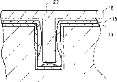
- H01L21/76841—Barrier, adhesion or liner layers
- H01L21/76843—Barrier, adhesion or liner layers formed in openings in a dielectric
-
- H—ELECTRICITY
- H01—ELECTRIC ELEMENTS
- H01L—SEMICONDUCTOR DEVICES NOT COVERED BY CLASS H10
- H01L21/00—Processes or apparatus adapted for the manufacture or treatment of semiconductor or solid state devices or of parts thereof
- H01L21/70—Manufacture or treatment of devices consisting of a plurality of solid state components formed in or on a common substrate or of parts thereof; Manufacture of integrated circuit devices or of parts thereof
- H01L21/71—Manufacture of specific parts of devices defined in group H01L21/70
- H01L21/768—Applying interconnections to be used for carrying current between separate components within a device comprising conductors and dielectrics
- H01L21/76838—Applying interconnections to be used for carrying current between separate components within a device comprising conductors and dielectrics characterised by the formation and the after-treatment of the conductors
- H01L21/76841—Barrier, adhesion or liner layers
- H01L21/76868—Forming or treating discontinuous thin films, e.g. repair, enhancement or reinforcement of discontinuous thin films
-
- H—ELECTRICITY
- H01—ELECTRIC ELEMENTS
- H01L—SEMICONDUCTOR DEVICES NOT COVERED BY CLASS H10
- H01L21/00—Processes or apparatus adapted for the manufacture or treatment of semiconductor or solid state devices or of parts thereof
- H01L21/70—Manufacture or treatment of devices consisting of a plurality of solid state components formed in or on a common substrate or of parts thereof; Manufacture of integrated circuit devices or of parts thereof
- H01L21/71—Manufacture of specific parts of devices defined in group H01L21/70
- H01L21/768—Applying interconnections to be used for carrying current between separate components within a device comprising conductors and dielectrics
- H01L21/76838—Applying interconnections to be used for carrying current between separate components within a device comprising conductors and dielectrics characterised by the formation and the after-treatment of the conductors
- H01L21/76841—Barrier, adhesion or liner layers
- H01L21/76871—Layers specifically deposited to enhance or enable the nucleation of further layers, i.e. seed layers
- H01L21/76873—Layers specifically deposited to enhance or enable the nucleation of further layers, i.e. seed layers for electroplating
-
- H—ELECTRICITY
- H01—ELECTRIC ELEMENTS
- H01L—SEMICONDUCTOR DEVICES NOT COVERED BY CLASS H10
- H01L21/00—Processes or apparatus adapted for the manufacture or treatment of semiconductor or solid state devices or of parts thereof
- H01L21/70—Manufacture or treatment of devices consisting of a plurality of solid state components formed in or on a common substrate or of parts thereof; Manufacture of integrated circuit devices or of parts thereof
- H01L21/71—Manufacture of specific parts of devices defined in group H01L21/70
- H01L21/768—Applying interconnections to be used for carrying current between separate components within a device comprising conductors and dielectrics
- H01L21/76838—Applying interconnections to be used for carrying current between separate components within a device comprising conductors and dielectrics characterised by the formation and the after-treatment of the conductors
- H01L21/76877—Filling of holes, grooves or trenches, e.g. vias, with conductive material
-
- H—ELECTRICITY
- H01—ELECTRIC ELEMENTS
- H01L—SEMICONDUCTOR DEVICES NOT COVERED BY CLASS H10
- H01L2221/00—Processes or apparatus adapted for the manufacture or treatment of semiconductor or solid state devices or of parts thereof covered by H01L21/00
- H01L2221/10—Applying interconnections to be used for carrying current between separate components within a device
- H01L2221/1068—Formation and after-treatment of conductors
- H01L2221/1073—Barrier, adhesion or liner layers
- H01L2221/1084—Layers specifically deposited to enhance or enable the nucleation of further layers, i.e. seed layers
- H01L2221/1089—Stacks of seed layers
-
- H—ELECTRICITY
- H05—ELECTRIC TECHNIQUES NOT OTHERWISE PROVIDED FOR
- H05K—PRINTED CIRCUITS; CASINGS OR CONSTRUCTIONAL DETAILS OF ELECTRIC APPARATUS; MANUFACTURE OF ASSEMBLAGES OF ELECTRICAL COMPONENTS
- H05K3/00—Apparatus or processes for manufacturing printed circuits
- H05K3/40—Forming printed elements for providing electric connections to or between printed circuits
- H05K3/42—Plated through-holes or plated via connections
- H05K3/423—Plated through-holes or plated via connections characterised by electroplating method
Abstract
Description
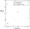
| Wafer | Solution when strengthening plating | Current density | Ununiformity standard deviation (%, 1 σ) |
| 1 | Citric acid | 3 minutes 2mA/cm 2 | 7.321 |
| 2 | EDTA | 3 minutes 2mA/cm 2 | 6.233 |
| 3 | Do not have | 0 | 46.10 |
Claims (50)
Applications Claiming Priority (4)
| Application Number | Priority Date | Filing Date | Title |
|---|---|---|---|
| US09/045,245 | 1998-03-20 | ||
| US09/045,245 US6197181B1 (en) | 1998-03-20 | 1998-03-20 | Apparatus and method for electrolytically depositing a metal on a microelectronic workpiece |
| US8567598P | 1998-05-15 | 1998-05-15 | |
| US60/085,675 | 1998-05-15 |
Publications (2)
| Publication Number | Publication Date |
|---|---|
| CN1293719A CN1293719A (en) | 2001-05-02 |
| CN1246504C true CN1246504C (en) | 2006-03-22 |
Family
ID=26722541
Family Applications (1)
| Application Number | Title | Priority Date | Filing Date |
|---|---|---|---|
| CNB998041289A Expired - Fee Related CN1246504C (en) | 1998-03-20 | 1999-03-22 | Apparatus and method for electrolytically depositing copper on semiconductor workpiece |
Country Status (7)
| Country | Link |
|---|---|
| US (6) | US6290833B1 (en) |
| EP (1) | EP1064417A4 (en) |
| JP (1) | JP4642229B2 (en) |
| KR (1) | KR100420157B1 (en) |
| CN (1) | CN1246504C (en) |
| TW (2) | TWI223678B (en) |
| WO (1) | WO1999047731A1 (en) |
Families Citing this family (172)
| Publication number | Priority date | Publication date | Assignee | Title |
|---|---|---|---|---|
| US7126195B1 (en) * | 1996-06-03 | 2006-10-24 | Micron Technology, Inc. | Method for forming a metallization layer |
| US6429120B1 (en) | 2000-01-18 | 2002-08-06 | Micron Technology, Inc. | Methods and apparatus for making integrated-circuit wiring from copper, silver, gold, and other metals |
| US6752584B2 (en) * | 1996-07-15 | 2004-06-22 | Semitool, Inc. | Transfer devices for handling microelectronic workpieces within an environment of a processing machine and methods of manufacturing and using such devices in the processing of microelectronic workpieces |
| US6921467B2 (en) * | 1996-07-15 | 2005-07-26 | Semitool, Inc. | Processing tools, components of processing tools, and method of making and using same for electrochemical processing of microelectronic workpieces |
| US7244677B2 (en) | 1998-02-04 | 2007-07-17 | Semitool. Inc. | Method for filling recessed micro-structures with metallization in the production of a microelectronic device |
| US6565729B2 (en) * | 1998-03-20 | 2003-05-20 | Semitool, Inc. | Method for electrochemically depositing metal on a semiconductor workpiece |
| US6197181B1 (en) | 1998-03-20 | 2001-03-06 | Semitool, Inc. | Apparatus and method for electrolytically depositing a metal on a microelectronic workpiece |
| TWI223678B (en) | 1998-03-20 | 2004-11-11 | Semitool Inc | Process for applying a metal structure to a workpiece, the treated workpiece and a solution for electroplating copper |
| EP1091024A4 (en) * | 1998-04-30 | 2006-03-22 | Ebara Corp | Method and device for plating substrate |
| US7338908B1 (en) | 2003-10-20 | 2008-03-04 | Novellus Systems, Inc. | Method for fabrication of semiconductor interconnect structure with reduced capacitance, leakage current, and improved breakdown voltage |
| CA2702148C (en) * | 1999-01-06 | 2014-03-04 | Genenews Inc. | Method of profiling gene expression in a human subject having an infectious disease |
| US6221763B1 (en) * | 1999-04-05 | 2001-04-24 | Micron Technology, Inc. | Method of forming a metal seed layer for subsequent plating |
| US6582578B1 (en) | 1999-04-08 | 2003-06-24 | Applied Materials, Inc. | Method and associated apparatus for tilting a substrate upon entry for metal deposition |
| US20060157355A1 (en) * | 2000-03-21 | 2006-07-20 | Semitool, Inc. | Electrolytic process using anion permeable barrier |
| CN1217034C (en) | 1999-04-13 | 2005-08-31 | 塞米用具公司 | Workpiece processor having processing chamber with improved processing fluid flow |
| US8852417B2 (en) | 1999-04-13 | 2014-10-07 | Applied Materials, Inc. | Electrolytic process using anion permeable barrier |
| US6916412B2 (en) * | 1999-04-13 | 2005-07-12 | Semitool, Inc. | Adaptable electrochemical processing chamber |
| US8236159B2 (en) * | 1999-04-13 | 2012-08-07 | Applied Materials Inc. | Electrolytic process using cation permeable barrier |
| US6159853A (en) * | 1999-08-04 | 2000-12-12 | Industrial Technology Research Institute | Method for using ultrasound for assisting forming conductive layers on semiconductor devices |
| US6413858B1 (en) | 1999-08-27 | 2002-07-02 | Micron Technology, Inc. | Barrier and electroplating seed layer |
| JP3498306B2 (en) * | 1999-09-16 | 2004-02-16 | 石原薬品株式会社 | Void-free copper plating method |
| US6423200B1 (en) | 1999-09-30 | 2002-07-23 | Lam Research Corporation | Copper interconnect seed layer treatment methods and apparatuses for treating the same |
| US6440849B1 (en) * | 1999-10-18 | 2002-08-27 | Agere Systems Guardian Corp. | Microstructure control of copper interconnects |
| KR100760337B1 (en) * | 1999-12-15 | 2007-09-20 | 롬 앤드 하스 일렉트로닉 머트어리얼즈, 엘.엘.씨 | Seed layer repair method |
| US6650957B1 (en) * | 2000-01-03 | 2003-11-18 | Advanced Micro Devices, Inc. | Method and apparatus for run-to-run control of deposition process |
| US6420262B1 (en) | 2000-01-18 | 2002-07-16 | Micron Technology, Inc. | Structures and methods to enhance copper metallization |
| US6376370B1 (en) * | 2000-01-18 | 2002-04-23 | Micron Technology, Inc. | Process for providing seed layers for using aluminum, copper, gold and silver metallurgy process for providing seed layers for using aluminum, copper, gold and silver metallurgy |
| US20060189129A1 (en) * | 2000-03-21 | 2006-08-24 | Semitool, Inc. | Method for applying metal features onto barrier layers using ion permeable barriers |
| US6582579B1 (en) * | 2000-03-24 | 2003-06-24 | Nutool, Inc. | Methods for repairing defects on a semiconductor substrate |
| US8475636B2 (en) * | 2008-11-07 | 2013-07-02 | Novellus Systems, Inc. | Method and apparatus for electroplating |
| EP1139396A3 (en) * | 2000-03-31 | 2003-08-27 | Texas Instruments Incorporated | Fixture and method for uniform electroless metal deposition on integrated circuit bond pads |
| US6913680B1 (en) | 2000-05-02 | 2005-07-05 | Applied Materials, Inc. | Method of application of electrical biasing to enhance metal deposition |
| EP1337693A2 (en) * | 2000-05-23 | 2003-08-27 | Applied Materials, Inc. | Method and apparatus to overcome anomalies in copper seed layers and to tune for feature size and aspect ratio |
| US20050006245A1 (en) | 2003-07-08 | 2005-01-13 | Applied Materials, Inc. | Multiple-step electrodeposition process for direct copper plating on barrier metals |
| US7273535B2 (en) * | 2003-09-17 | 2007-09-25 | Applied Materials, Inc. | Insoluble anode with an auxiliary electrode |
| US20050284751A1 (en) * | 2004-06-28 | 2005-12-29 | Nicolay Kovarsky | Electrochemical plating cell with a counter electrode in an isolated anolyte compartment |
| US20050145499A1 (en) * | 2000-06-05 | 2005-07-07 | Applied Materials, Inc. | Plating of a thin metal seed layer |
| US20050109627A1 (en) * | 2003-10-10 | 2005-05-26 | Applied Materials, Inc. | Methods and chemistry for providing initial conformal electrochemical deposition of copper in sub-micron features |
| TW562878B (en) * | 2000-06-30 | 2003-11-21 | Ebara Corp | Copper-plating liquid, plating method and plating apparatus |
| US6660153B2 (en) * | 2000-10-20 | 2003-12-09 | Shipley Company, L.L.C. | Seed layer repair bath |
| US20020090484A1 (en) * | 2000-10-20 | 2002-07-11 | Shipley Company, L.L.C. | Plating bath |
| US6660154B2 (en) | 2000-10-25 | 2003-12-09 | Shipley Company, L.L.C. | Seed layer |
| US6824665B2 (en) * | 2000-10-25 | 2004-11-30 | Shipley Company, L.L.C. | Seed layer deposition |
| US6797146B2 (en) | 2000-11-02 | 2004-09-28 | Shipley Company, L.L.C. | Seed layer repair |
| EP1215305B1 (en) | 2000-12-13 | 2010-05-05 | Imec | Method for preparing an electroplating bath and related copper plating process |
| AU2002248343A1 (en) * | 2001-01-12 | 2002-08-19 | University Of Rochester | Methods and systems for electro-or electroless-plating of metal in high-aspect ratio features |
| JP2002289559A (en) * | 2001-02-01 | 2002-10-04 | Texas Instr Inc <Ti> | Production method for integrated circuit |
| CN1253606C (en) * | 2001-02-23 | 2006-04-26 | 株式会社荏原制作所 | Copper-plating solution, plating method and plating apparatus |
| US20050081744A1 (en) * | 2003-10-16 | 2005-04-21 | Semitool, Inc. | Electroplating compositions and methods for electroplating |
| US6730857B2 (en) | 2001-03-13 | 2004-05-04 | International Business Machines Corporation | Structure having laser ablated features and method of fabricating |
| US6740221B2 (en) | 2001-03-15 | 2004-05-25 | Applied Materials Inc. | Method of forming copper interconnects |
| TW529090B (en) | 2001-04-04 | 2003-04-21 | Koninkl Philips Electronics Nv | Back-end metallisation process |
| US6506668B1 (en) * | 2001-06-22 | 2003-01-14 | Advanced Micro Devices, Inc. | Utilization of annealing enhanced or repaired seed layer to improve copper interconnect reliability |
| US6664122B1 (en) | 2001-10-19 | 2003-12-16 | Novellus Systems, Inc. | Electroless copper deposition method for preparing copper seed layers |
| US20050051432A1 (en) * | 2001-12-13 | 2005-03-10 | Mitsuhiko Shirakashi | Electrolytic processing apparatus and method |
| AU2003217197A1 (en) * | 2002-01-10 | 2003-07-30 | Semitool, Inc. | Method for applying metal features onto barrier layers using electrochemical deposition |
| US7239747B2 (en) * | 2002-01-24 | 2007-07-03 | Chatterbox Systems, Inc. | Method and system for locating position in printed texts and delivering multimedia information |
| TWI275436B (en) * | 2002-01-31 | 2007-03-11 | Ebara Corp | Electrochemical machining device, and substrate processing apparatus and method |
| US20030188974A1 (en) * | 2002-04-03 | 2003-10-09 | Applied Materials, Inc. | Homogeneous copper-tin alloy plating for enhancement of electro-migration resistance in interconnects |
| US20030201185A1 (en) * | 2002-04-29 | 2003-10-30 | Applied Materials, Inc. | In-situ pre-clean for electroplating process |
| US6911136B2 (en) * | 2002-04-29 | 2005-06-28 | Applied Materials, Inc. | Method for regulating the electrical power applied to a substrate during an immersion process |
| US6893505B2 (en) * | 2002-05-08 | 2005-05-17 | Semitool, Inc. | Apparatus and method for regulating fluid flows, such as flows of electrochemical processing fluids |
| US6875331B2 (en) * | 2002-07-11 | 2005-04-05 | Applied Materials, Inc. | Anode isolation by diffusion differentials |
| US20040217005A1 (en) * | 2002-07-24 | 2004-11-04 | Aron Rosenfeld | Method for electroplating bath chemistry control |
| US7128823B2 (en) | 2002-07-24 | 2006-10-31 | Applied Materials, Inc. | Anolyte for copper plating |
| US7247222B2 (en) * | 2002-07-24 | 2007-07-24 | Applied Materials, Inc. | Electrochemical processing cell |
| US7223323B2 (en) * | 2002-07-24 | 2007-05-29 | Applied Materials, Inc. | Multi-chemistry plating system |
| US7025866B2 (en) | 2002-08-21 | 2006-04-11 | Micron Technology, Inc. | Microelectronic workpiece for electrochemical deposition processing and methods of manufacturing and using such microelectronic workpieces |
| US7897198B1 (en) | 2002-09-03 | 2011-03-01 | Novellus Systems, Inc. | Electroless layer plating process and apparatus |
| US20040118699A1 (en) * | 2002-10-02 | 2004-06-24 | Applied Materials, Inc. | Homogeneous copper-palladium alloy plating for enhancement of electro-migration resistance in interconnects |
| US7902062B2 (en) | 2002-11-23 | 2011-03-08 | Infineon Technologies Ag | Electrodepositing a metal in integrated circuit applications |
| DE10254815A1 (en) * | 2002-11-23 | 2004-06-09 | Infineon Technologies Ag | Process for the galvanic application of a metal, in particular copper, use of this process and integrated circuit arrangement |
| US7147767B2 (en) * | 2002-12-16 | 2006-12-12 | 3M Innovative Properties Company | Plating solutions for electrochemical or chemical deposition of copper interconnects and methods therefor |
| US6884338B2 (en) * | 2002-12-16 | 2005-04-26 | 3M Innovative Properties Company | Methods for polishing and/or cleaning copper interconnects and/or film and compositions therefor |
| US6858124B2 (en) * | 2002-12-16 | 2005-02-22 | 3M Innovative Properties Company | Methods for polishing and/or cleaning copper interconnects and/or film and compositions therefor |
| US7198705B2 (en) * | 2002-12-19 | 2007-04-03 | Texas Instruments Incorporated | Plating-rinse-plating process for fabricating copper interconnects |
| US20040154926A1 (en) * | 2002-12-24 | 2004-08-12 | Zhi-Wen Sun | Multiple chemistry electrochemical plating method |
| US20040200725A1 (en) * | 2003-04-09 | 2004-10-14 | Applied Materials Inc. | Application of antifoaming agent to reduce defects in a semiconductor electrochemical plating process |
| US20040206628A1 (en) * | 2003-04-18 | 2004-10-21 | Applied Materials, Inc. | Electrical bias during wafer exit from electrolyte bath |
| US7473339B2 (en) * | 2003-04-18 | 2009-01-06 | Applied Materials, Inc. | Slim cell platform plumbing |
| US7311810B2 (en) * | 2003-04-18 | 2007-12-25 | Applied Materials, Inc. | Two position anneal chamber |
| US7297247B2 (en) * | 2003-05-06 | 2007-11-20 | Applied Materials, Inc. | Electroformed sputtering target |
| US20040253386A1 (en) * | 2003-06-13 | 2004-12-16 | Sarojini Deevi | Preparation of intermetallics by metallo-organic decomposition |
| KR100545192B1 (en) * | 2003-06-19 | 2006-01-24 | 동부아남반도체 주식회사 | Deposition stop time detect apparatus and copper wiring formation apparatus of semiconductor device using the same |
| US20070125657A1 (en) * | 2003-07-08 | 2007-06-07 | Zhi-Wen Sun | Method of direct plating of copper on a substrate structure |
| US20060283716A1 (en) * | 2003-07-08 | 2006-12-21 | Hooman Hafezi | Method of direct plating of copper on a ruthenium alloy |
| US7654221B2 (en) | 2003-10-06 | 2010-02-02 | Applied Materials, Inc. | Apparatus for electroless deposition of metals onto semiconductor substrates |
| US7827930B2 (en) | 2004-01-26 | 2010-11-09 | Applied Materials, Inc. | Apparatus for electroless deposition of metals onto semiconductor substrates |
| US20050085031A1 (en) * | 2003-10-15 | 2005-04-21 | Applied Materials, Inc. | Heterogeneous activation layers formed by ionic and electroless reactions used for IC interconnect capping layers |
| US8372757B2 (en) | 2003-10-20 | 2013-02-12 | Novellus Systems, Inc. | Wet etching methods for copper removal and planarization in semiconductor processing |
| US7972970B2 (en) | 2003-10-20 | 2011-07-05 | Novellus Systems, Inc. | Fabrication of semiconductor interconnect structure |
| US20050092611A1 (en) * | 2003-11-03 | 2005-05-05 | Semitool, Inc. | Bath and method for high rate copper deposition |
| US20050092616A1 (en) * | 2003-11-03 | 2005-05-05 | Semitool, Inc. | Baths, methods, and tools for superconformal deposition of conductive materials other than copper |
| US7205233B2 (en) | 2003-11-07 | 2007-04-17 | Applied Materials, Inc. | Method for forming CoWRe alloys by electroless deposition |
| US7214297B2 (en) | 2004-06-28 | 2007-05-08 | Applied Materials, Inc. | Substrate support element for an electrochemical plating cell |
| US20060045666A1 (en) * | 2004-07-09 | 2006-03-02 | Harris Randy A | Modular tool unit for processing of microfeature workpieces |
| EP1842939B1 (en) | 2005-01-25 | 2011-02-09 | Nippon Mining & Metals Co., Ltd. | Copper electrolysis solution containing compound having specific skeleton as additive, and electrolytic copper foil produced therefrom |
| US7438949B2 (en) * | 2005-01-27 | 2008-10-21 | Applied Materials, Inc. | Ruthenium containing layer deposition method |
| US20060162658A1 (en) * | 2005-01-27 | 2006-07-27 | Applied Materials, Inc. | Ruthenium layer deposition apparatus and method |
| US20060246217A1 (en) | 2005-03-18 | 2006-11-02 | Weidman Timothy W | Electroless deposition process on a silicide contact |
| US7651934B2 (en) | 2005-03-18 | 2010-01-26 | Applied Materials, Inc. | Process for electroless copper deposition |
| TW200707640A (en) | 2005-03-18 | 2007-02-16 | Applied Materials Inc | Contact metallization scheme using a barrier layer over a silicide layer |
| FR2890984B1 (en) * | 2005-09-20 | 2009-03-27 | Alchimer Sa | ELECTRODEPOSITION PROCESS FOR COATING A SURFACE OF A SUBSTRATE WITH A METAL |
| FR2890983B1 (en) * | 2005-09-20 | 2007-12-14 | Alchimer Sa | ELECTRODEPOSITION COMPOSITION FOR COATING A SURFACE OF A SUBSTRATE WITH A METAL |
| US20070071888A1 (en) * | 2005-09-21 | 2007-03-29 | Arulkumar Shanmugasundram | Method and apparatus for forming device features in an integrated electroless deposition system |
| US7456102B1 (en) | 2005-10-11 | 2008-11-25 | Novellus Systems, Inc. | Electroless copper fill process |
| US7605082B1 (en) | 2005-10-13 | 2009-10-20 | Novellus Systems, Inc. | Capping before barrier-removal IC fabrication method |
| US9127362B2 (en) | 2005-10-31 | 2015-09-08 | Applied Materials, Inc. | Process kit and target for substrate processing chamber |
| US8647484B2 (en) | 2005-11-25 | 2014-02-11 | Applied Materials, Inc. | Target for sputtering chamber |
| US7579274B2 (en) * | 2006-02-21 | 2009-08-25 | Alchimer | Method and compositions for direct copper plating and filing to form interconnects in the fabrication of semiconductor devices |
| US7655126B2 (en) | 2006-03-27 | 2010-02-02 | Federal Mogul World Wide, Inc. | Fabrication of topical stopper on MLS gasket by active matrix electrochemical deposition |
| EP1845554A3 (en) * | 2006-04-10 | 2011-07-13 | Imec | A method to create super secondary grain growth in narrow trenches |
| US9822461B2 (en) | 2006-08-16 | 2017-11-21 | Novellus Systems, Inc. | Dynamic current distribution control apparatus and method for wafer electroplating |
| US7799684B1 (en) | 2007-03-05 | 2010-09-21 | Novellus Systems, Inc. | Two step process for uniform across wafer deposition and void free filling on ruthenium coated wafers |
| US20080264774A1 (en) * | 2007-04-25 | 2008-10-30 | Semitool, Inc. | Method for electrochemically depositing metal onto a microelectronic workpiece |
| US8968536B2 (en) | 2007-06-18 | 2015-03-03 | Applied Materials, Inc. | Sputtering target having increased life and sputtering uniformity |
| JP5358145B2 (en) * | 2007-09-28 | 2013-12-04 | 富士フイルム株式会社 | Conductive material manufacturing method and conductive material manufacturing apparatus |
| US7901552B2 (en) | 2007-10-05 | 2011-03-08 | Applied Materials, Inc. | Sputtering target with grooves and intersecting channels |
| US8237892B1 (en) | 2007-11-30 | 2012-08-07 | Sipix Imaging, Inc. | Display device with a brightness enhancement structure |
| US7830592B1 (en) * | 2007-11-30 | 2010-11-09 | Sipix Imaging, Inc. | Display devices having micro-reflectors |
| US8118988B2 (en) * | 2008-01-31 | 2012-02-21 | Eci Technology, Inc. | Analysis of copper ion and complexing agent in copper plating baths |
| US7964506B1 (en) * | 2008-03-06 | 2011-06-21 | Novellus Systems, Inc. | Two step copper electroplating process with anneal for uniform across wafer deposition and void free filling on ruthenium coated wafers |
| US8513124B1 (en) | 2008-03-06 | 2013-08-20 | Novellus Systems, Inc. | Copper electroplating process for uniform across wafer deposition and void free filling on semi-noble metal coated wafers |
| US8703615B1 (en) | 2008-03-06 | 2014-04-22 | Novellus Systems, Inc. | Copper electroplating process for uniform across wafer deposition and void free filling on ruthenium coated wafers |
| US8437069B2 (en) * | 2008-03-11 | 2013-05-07 | Sipix Imaging, Inc. | Luminance enhancement structure for reflective display devices |
| WO2009114361A1 (en) | 2008-03-11 | 2009-09-17 | Sipix Imaging, Inc. | Luminance enhancement structure for reflective display devices |
| US8858774B2 (en) | 2008-11-07 | 2014-10-14 | Novellus Systems, Inc. | Electroplating apparatus for tailored uniformity profile |
| US8107254B2 (en) * | 2008-11-20 | 2012-01-31 | International Business Machines Corporation | Integrating capacitors into vias of printed circuit boards |
| US8441414B2 (en) * | 2008-12-05 | 2013-05-14 | Sipix Imaging, Inc. | Luminance enhancement structure with Moiré reducing design |
| US9025234B2 (en) * | 2009-01-22 | 2015-05-05 | E Ink California, Llc | Luminance enhancement structure with varying pitches |
| CN102395712A (en) | 2009-02-12 | 2012-03-28 | 技术研究及发展基金有限公司 | A process for electroplating of copper |
| US8120836B2 (en) * | 2009-03-09 | 2012-02-21 | Sipix Imaging, Inc. | Luminance enhancement structure for reflective display devices |
| US8714780B2 (en) * | 2009-04-22 | 2014-05-06 | Sipix Imaging, Inc. | Display devices with grooved luminance enhancement film |
| JP5388191B2 (en) * | 2009-05-26 | 2014-01-15 | Jx日鉱日石金属株式会社 | Plating object having through silicon via and method for forming the same |
| US8797633B1 (en) | 2009-07-23 | 2014-08-05 | Sipix Imaging, Inc. | Display device assembly and manufacture thereof |
| US8456589B1 (en) | 2009-07-27 | 2013-06-04 | Sipix Imaging, Inc. | Display device assembly |
| KR20120080595A (en) | 2009-09-02 | 2012-07-17 | 노벨러스 시스템즈, 인코포레이티드 | Reduced isotropic etchant material consumption and waste generation |
| US8242384B2 (en) | 2009-09-30 | 2012-08-14 | International Business Machines Corporation | Through hole-vias in multi-layer printed circuit boards |
| JP2011097038A (en) * | 2009-10-02 | 2011-05-12 | Ibiden Co Ltd | Ceramic wiring substrate and manufacturing method of the same |
| US8432027B2 (en) * | 2009-11-11 | 2013-04-30 | International Business Machines Corporation | Integrated circuit die stacks with rotationally symmetric vias |
| US8315068B2 (en) | 2009-11-12 | 2012-11-20 | International Business Machines Corporation | Integrated circuit die stacks having initially identical dies personalized with fuses and methods of manufacturing the same |
| US8310841B2 (en) | 2009-11-12 | 2012-11-13 | International Business Machines Corporation | Integrated circuit die stacks having initially identical dies personalized with switches and methods of making the same |
| US8258619B2 (en) | 2009-11-12 | 2012-09-04 | International Business Machines Corporation | Integrated circuit die stacks with translationally compatible vias |
| US9646947B2 (en) * | 2009-12-22 | 2017-05-09 | Lenovo Enterprise Solutions (Singapore) Pte. Ltd. | Integrated circuit with inductive bond wires |
| US8168540B1 (en) * | 2009-12-29 | 2012-05-01 | Novellus Systems, Inc. | Methods and apparatus for depositing copper on tungsten |
| US20110192462A1 (en) * | 2010-01-03 | 2011-08-11 | Alchimer, S.A. | Solar cells |
| US20110162701A1 (en) * | 2010-01-03 | 2011-07-07 | Claudio Truzzi | Photovoltaic Cells |
| JP5750626B2 (en) * | 2010-03-19 | 2015-07-22 | 石原ケミカル株式会社 | Electro copper plating method |
| US9714474B2 (en) * | 2010-04-06 | 2017-07-25 | Tel Nexx, Inc. | Seed layer deposition in microscale features |
| US9005409B2 (en) | 2011-04-14 | 2015-04-14 | Tel Nexx, Inc. | Electro chemical deposition and replenishment apparatus |
| US9017528B2 (en) | 2011-04-14 | 2015-04-28 | Tel Nexx, Inc. | Electro chemical deposition and replenishment apparatus |
| US8575028B2 (en) | 2011-04-15 | 2013-11-05 | Novellus Systems, Inc. | Method and apparatus for filling interconnect structures |
| US8496790B2 (en) * | 2011-05-18 | 2013-07-30 | Applied Materials, Inc. | Electrochemical processor |
| CN102251269B (en) * | 2011-08-19 | 2013-07-03 | 银都餐饮设备股份有限公司 | Electrochemical surface treatment device |
| JP6021441B2 (en) | 2012-05-25 | 2016-11-09 | ラピスセミコンダクタ株式会社 | Semiconductor device |
| US9909228B2 (en) | 2012-11-27 | 2018-03-06 | Lam Research Corporation | Method and apparatus for dynamic current distribution control during electroplating |
| US9670588B2 (en) | 2013-05-01 | 2017-06-06 | Lam Research Corporation | Anisotropic high resistance ionic current source (AHRICS) |
| TWI653367B (en) * | 2013-06-11 | 2019-03-11 | 美商應用材料股份有限公司 | Electrochemical deposition on a workpiece having high sheet resistance |
| US9303329B2 (en) | 2013-11-11 | 2016-04-05 | Tel Nexx, Inc. | Electrochemical deposition apparatus with remote catholyte fluid management |
| US20150197870A1 (en) * | 2014-01-15 | 2015-07-16 | The Board Of Trustees Of The Leland Stanford Junior University | Method for Plating Fine Grain Copper Deposit on Metal Substrate |
| KR102041646B1 (en) * | 2014-05-13 | 2019-11-07 | 삼성전기주식회사 | Electrode structure |
| CN104313657A (en) * | 2014-11-10 | 2015-01-28 | 临安振有电子有限公司 | Electro-deposition device of through hole of HDI printed circuit board |
| US10648096B2 (en) * | 2014-12-12 | 2020-05-12 | Infineon Technologies Ag | Electrolyte, method of forming a copper layer and method of forming a chip |
| US9752248B2 (en) | 2014-12-19 | 2017-09-05 | Lam Research Corporation | Methods and apparatuses for dynamically tunable wafer-edge electroplating |
| US9816194B2 (en) | 2015-03-19 | 2017-11-14 | Lam Research Corporation | Control of electrolyte flow dynamics for uniform electroplating |
| DE102016113641A1 (en) * | 2016-07-25 | 2018-01-25 | Christian-Albrechts-Universität Zu Kiel | Aluminum-copper connector having a heterostructure and method of making the heterostructure |
| JP6272431B2 (en) * | 2016-10-04 | 2018-01-31 | ラピスセミコンダクタ株式会社 | Semiconductor device and manufacturing method thereof |
| US10930511B2 (en) * | 2018-03-30 | 2021-02-23 | Lam Research Corporation | Copper electrodeposition sequence for the filling of cobalt lined features |
| JP6926294B2 (en) * | 2018-11-29 | 2021-08-25 | ラピスセミコンダクタ株式会社 | Manufacturing method of semiconductor devices |
| CN111315146A (en) * | 2020-02-27 | 2020-06-19 | 清华大学 | Method for manufacturing flexible composite circuit |
| CN113363152A (en) * | 2020-03-06 | 2021-09-07 | 长鑫存储技术有限公司 | Semiconductor structure and manufacturing method thereof |
| CN115498050B (en) * | 2022-09-23 | 2024-03-29 | 通威太阳能(成都)有限公司 | Solar cell and preparation method thereof |
Family Cites Families (168)
| Publication number | Priority date | Publication date | Assignee | Title |
|---|---|---|---|---|
| US1526644A (en) * | 1922-10-25 | 1925-02-17 | Williams Brothers Mfg Company | Process of electroplating and apparatus therefor |
| US2411674A (en) * | 1943-03-04 | 1946-11-26 | Little Inc A | Art of electrodeposition of copper |
| NL170870B (en) * | 1952-07-05 | Koninklijke Hoogovens En Staal | PROCESS FOR FIRE-PROOF CLADING OF OVEN WALLS AND AN THIS MANUFACTURED METALLURGIC SHAFT OVEN. | |
| NL291575A (en) | 1962-04-16 | |||
| US3309263A (en) * | 1964-12-03 | 1967-03-14 | Kimberly Clark Co | Web pickup and transfer for a papermaking machine |
| US3328273A (en) | 1966-08-15 | 1967-06-27 | Udylite Corp | Electro-deposition of copper from acidic baths |
| US3495940A (en) * | 1967-09-28 | 1970-02-17 | Celanese Corp | Production of high temperature resistant continuous filaments |
| US3664933A (en) * | 1969-06-19 | 1972-05-23 | Udylite Corp | Process for acid copper plating of zinc |
| US3684666A (en) * | 1970-03-19 | 1972-08-15 | Pfizer & Co C | Copper electroplating in a citric acid bath |
| US3716462A (en) * | 1970-10-05 | 1973-02-13 | D Jensen | Copper plating on zinc and its alloys |
| US3930963A (en) * | 1971-07-29 | 1976-01-06 | Photocircuits Division Of Kollmorgen Corporation | Method for the production of radiant energy imaged printed circuit boards |
| BE791401A (en) * | 1971-11-15 | 1973-05-14 | Monsanto Co | ELECTROCHEMICAL COMPOSITIONS AND PROCESSES |
| US3770598A (en) | 1972-01-21 | 1973-11-06 | Oxy Metal Finishing Corp | Electrodeposition of copper from acid baths |
| US3798003A (en) * | 1972-02-14 | 1974-03-19 | E Ensley | Differential microcalorimeter |
| DE2244434C3 (en) * | 1972-09-06 | 1982-02-25 | Schering Ag, 1000 Berlin Und 4619 Bergkamen | Aqueous bath for the galvanic deposition of gold and gold alloys |
| US4022679A (en) * | 1973-05-10 | 1977-05-10 | C. Conradty | Coated titanium anode for amalgam heavy duty cells |
| US4001094A (en) * | 1974-09-19 | 1977-01-04 | Jumer John F | Method for incremental electro-processing of large areas |
| US4072557A (en) * | 1974-12-23 | 1978-02-07 | J. M. Voith Gmbh | Method and apparatus for shrinking a travelling web of fibrous material |
| US4000046A (en) | 1974-12-23 | 1976-12-28 | P. R. Mallory & Co., Inc. | Method of electroplating a conductive layer over an electrolytic capacitor |
| JPS5216433A (en) | 1975-07-30 | 1977-02-07 | Furukawa Electric Co Ltd | Method of producing very thin copper foil |
| US4137867A (en) * | 1977-09-12 | 1979-02-06 | Seiichiro Aigo | Apparatus for bump-plating semiconductor wafers |
| US4134802A (en) | 1977-10-03 | 1979-01-16 | Oxy Metal Industries Corporation | Electrolyte and method for electrodepositing bright metal deposits |
| US4279948A (en) | 1978-05-25 | 1981-07-21 | Macdermid Incorporated | Electroless copper deposition solution using a hypophosphite reducing agent |
| US4246088A (en) * | 1979-01-24 | 1981-01-20 | Metal Box Limited | Method and apparatus for electrolytic treatment of containers |
| SU921124A1 (en) | 1979-06-19 | 1982-04-15 | Институт Физико-Химических Основ Переработки Минерального Сырья Со Ан Ссср | Method of metallization of printed circuit board apertures |
| US4272335A (en) | 1980-02-19 | 1981-06-09 | Oxy Metal Industries Corporation | Composition and method for electrodeposition of copper |
| US4259166A (en) * | 1980-03-31 | 1981-03-31 | Rca Corporation | Shield for plating substrate |
| US4437943A (en) * | 1980-07-09 | 1984-03-20 | Olin Corporation | Method and apparatus for bonding metal wire to a base metal substrate |
| EP0047132B1 (en) * | 1980-09-02 | 1985-07-03 | Heraeus Quarzschmelze Gmbh | Method of and apparatus for transferring semiconductor wafers between carrier members |
| US4323433A (en) * | 1980-09-22 | 1982-04-06 | The Boeing Company | Anodizing process employing adjustable shield for suspended cathode |
| US4443117A (en) * | 1980-09-26 | 1984-04-17 | Terumo Corporation | Measuring apparatus, method of manufacture thereof, and method of writing data into same |
| JPS57198315U (en) * | 1981-06-12 | 1982-12-16 | ||
| JPS584382A (en) * | 1981-06-26 | 1983-01-11 | ファナック株式会社 | Control system for industrial robot |
| US4378283A (en) * | 1981-07-30 | 1983-03-29 | National Semiconductor Corporation | Consumable-anode selective plating apparatus |
| US4384930A (en) * | 1981-08-21 | 1983-05-24 | Mcgean-Rohco, Inc. | Electroplating baths, additives therefor and methods for the electrodeposition of metals |
| JPS58149189A (en) * | 1982-03-01 | 1983-09-05 | セイコーインスツルメンツ株式会社 | Turning lifting mechanism of industrial robot |
| US4440597A (en) * | 1982-03-15 | 1984-04-03 | The Procter & Gamble Company | Wet-microcontracted paper and concomitant process |
| US4449885A (en) * | 1982-05-24 | 1984-05-22 | Varian Associates, Inc. | Wafer transfer system |
| US4451197A (en) * | 1982-07-26 | 1984-05-29 | Advanced Semiconductor Materials Die Bonding, Inc. | Object detection apparatus and method |
| US4585539A (en) * | 1982-08-17 | 1986-04-29 | Technic, Inc. | Electrolytic reactor |
| US4500394A (en) * | 1984-05-16 | 1985-02-19 | At&T Technologies, Inc. | Contacting a surface for plating thereon |
| US4673469A (en) * | 1984-06-08 | 1987-06-16 | Mcgean-Rohco, Inc. | Method of plating plastics |
| US4634503A (en) * | 1984-06-27 | 1987-01-06 | Daniel Nogavich | Immersion electroplating system |
| US4639028A (en) * | 1984-11-13 | 1987-01-27 | Economic Development Corporation | High temperature and acid resistant wafer pick up device |
| DE3500005A1 (en) * | 1985-01-02 | 1986-07-10 | ESB Elektrostatische Sprüh- und Beschichtungsanlagen G.F. Vöhringer GmbH, 7758 Meersburg | COATING CABIN FOR COATING THE SURFACE OF WORKPIECES WITH COATING POWDER |
| US4576685A (en) * | 1985-04-23 | 1986-03-18 | Schering Ag | Process and apparatus for plating onto articles |
| US4648944A (en) * | 1985-07-18 | 1987-03-10 | Martin Marietta Corporation | Apparatus and method for controlling plating induced stress in electroforming and electroplating processes |
| US4624749A (en) | 1985-09-03 | 1986-11-25 | Harris Corporation | Electrodeposition of submicrometer metallic interconnect for integrated circuits |
| FR2587915B1 (en) * | 1985-09-27 | 1987-11-27 | Omya Sa | DEVICE FOR CONTACTING FLUIDS IN THE FORM OF DIFFERENT PHASES |
| JPH088723B2 (en) * | 1985-11-02 | 1996-01-29 | 日立機電工業株式会社 | Conveyor device using linear motor |
| BR8607061A (en) * | 1985-12-24 | 1988-02-23 | Gould Inc | PROCESS AND APPLIANCE FOR ELECTROGALVANIZATION OF COPPER SHEET |
| JP2624703B2 (en) * | 1987-09-24 | 1997-06-25 | 株式会社東芝 | Method and apparatus for forming bump |
| DE3735449A1 (en) * | 1987-10-20 | 1989-05-03 | Convac Gmbh | MANUFACTURING SYSTEM FOR SEMICONDUCTOR SUBSTRATES |
| US4902398A (en) * | 1988-04-27 | 1990-02-20 | American Thim Film Laboratories, Inc. | Computer program for vacuum coating systems |
| US5235995A (en) * | 1989-03-27 | 1993-08-17 | Semitool, Inc. | Semiconductor processor apparatus with dynamic wafer vapor treatment and particulate volatilization |
| US4988533A (en) * | 1988-05-27 | 1991-01-29 | Texas Instruments Incorporated | Method for deposition of silicon oxide on a wafer |
| DE3818757A1 (en) * | 1988-05-31 | 1989-12-07 | Mannesmann Ag | PORTAL OF AN INDUSTRIAL ROBOT |
| US4959278A (en) * | 1988-06-16 | 1990-09-25 | Nippon Mining Co., Ltd. | Tin whisker-free tin or tin alloy plated article and coating technique thereof |
| US4990224A (en) | 1988-12-21 | 1991-02-05 | International Business Machines Corporation | Copper plating bath and process for difficult to plate metals |
| US5021129A (en) | 1989-09-25 | 1991-06-04 | International Business Machines Corporation | Multilayer structures of different electroactive materials and methods of fabrication thereof |
| JPH03125453A (en) * | 1989-10-09 | 1991-05-28 | Toshiba Corp | Semiconductor wafer transfer device |
| US5000827A (en) * | 1990-01-02 | 1991-03-19 | Motorola, Inc. | Method and apparatus for adjusting plating solution flow characteristics at substrate cathode periphery to minimize edge effect |
| DE69102553T2 (en) * | 1990-02-09 | 1994-10-20 | Nihon Parkerizing | Process for the surface treatment of titanium-containing metal objects. |
| JPH04120290A (en) * | 1990-02-26 | 1992-04-21 | Ishihara Chem Co Ltd | Copper electroplating solution |
| US5186594A (en) * | 1990-04-19 | 1993-02-16 | Applied Materials, Inc. | Dual cassette load lock |
| US5370741A (en) * | 1990-05-15 | 1994-12-06 | Semitool, Inc. | Dynamic semiconductor wafer processing using homogeneous chemical vapors |
| KR0153250B1 (en) * | 1990-06-28 | 1998-12-01 | 카자마 겐쥬 | Vertical heat-treating apparatus |
| US5368711A (en) * | 1990-08-01 | 1994-11-29 | Poris; Jaime | Selective metal electrodeposition process and apparatus |
| JP2524436B2 (en) * | 1990-09-18 | 1996-08-14 | インターナショナル・ビジネス・マシーンズ・コーポレイション | Surface treatment method |
| US5115430A (en) | 1990-09-24 | 1992-05-19 | At&T Bell Laboratories | Fair access of multi-priority traffic to distributed-queue dual-bus networks |
| US5151168A (en) * | 1990-09-24 | 1992-09-29 | Micron Technology, Inc. | Process for metallizing integrated circuits with electrolytically-deposited copper |
| US5078852A (en) * | 1990-10-12 | 1992-01-07 | Microelectronics And Computer Technology Corporation | Plating rack |
| US5096550A (en) * | 1990-10-15 | 1992-03-17 | The United States Of America As Represented By The United States Department Of Energy | Method and apparatus for spatially uniform electropolishing and electrolytic etching |
| JP2768390B2 (en) | 1990-12-11 | 1998-06-25 | インターナショナル・ビジネス・マシーンズ・コーポレイション | Method of conditioning a substrate for electroless metal deposition |
| DE69220519T2 (en) * | 1991-03-04 | 1998-02-19 | Toda Kogyo Corp | Process for plating a bonded magnet and bonded magnet with a metal coating |
| EP1120817B8 (en) * | 1991-03-26 | 2007-10-10 | Ngk Insulators, Ltd. | Use of a corrosion-resistant member |
| US5178512A (en) * | 1991-04-01 | 1993-01-12 | Equipe Technologies | Precision robot apparatus |
| JPH0544075A (en) * | 1991-08-15 | 1993-02-23 | Nippon Riironaale Kk | Copper striking method substituted for electroless copper plating |
| US5209817A (en) * | 1991-08-22 | 1993-05-11 | International Business Machines Corporation | Selective plating method for forming integral via and wiring layers |
| US5399564A (en) * | 1991-09-03 | 1995-03-21 | Dowelanco | N-(4-pyridyl or 4-quinolinyl) arylacetamide and 4-(aralkoxy or aralkylamino) pyridine pesticides |
| JP3057186B2 (en) | 1991-11-22 | 2000-06-26 | 横河電機株式会社 | Waveform analyzer |
| US5252196A (en) * | 1991-12-05 | 1993-10-12 | Shipley Company Inc. | Copper electroplating solutions and processes |
| US5301700A (en) * | 1992-03-05 | 1994-04-12 | Tokyo Electron Limited | Washing system |
| US5501768A (en) * | 1992-04-17 | 1996-03-26 | Kimberly-Clark Corporation | Method of treating papermaking fibers for making tissue |
| EP0582019B1 (en) * | 1992-08-04 | 1995-10-18 | International Business Machines Corporation | Fully automated and computerized conveyor based manufacturing line architectures adapted to pressurized sealable transportable containers |
| US5372848A (en) * | 1992-12-24 | 1994-12-13 | International Business Machines Corporation | Process for creating organic polymeric substrate with copper |
| US5302278A (en) * | 1993-02-19 | 1994-04-12 | Learonal, Inc. | Cyanide-free plating solutions for monovalent metals |
| US5284548A (en) | 1993-03-03 | 1994-02-08 | Microelectronics And Computer Technology Corporation | Process for producing electrical circuits with precision surface features |
| US5719447A (en) | 1993-06-03 | 1998-02-17 | Intel Corporation | Metal alloy interconnections for integrated circuits |
| JPH06349952A (en) * | 1993-06-14 | 1994-12-22 | Oki Electric Ind Co Ltd | Wiring forming method |
| US5489341A (en) * | 1993-08-23 | 1996-02-06 | Semitool, Inc. | Semiconductor processing with non-jetting fluid stream discharge array |
| US5472502A (en) | 1993-08-30 | 1995-12-05 | Semiconductor Systems, Inc. | Apparatus and method for spin coating wafers and the like |
| US5391517A (en) * | 1993-09-13 | 1995-02-21 | Motorola Inc. | Process for forming copper interconnect structure |
| US5409587A (en) | 1993-09-16 | 1995-04-25 | Micron Technology, Inc. | Sputtering with collinator cleaning within the sputtering chamber |
| ATE163453T1 (en) * | 1993-11-16 | 1998-03-15 | Scapa Group Plc | PAPER MACHINE CLOTHING |
| JPH07193214A (en) * | 1993-12-27 | 1995-07-28 | Mitsubishi Electric Corp | Via-hole and its formation |
| US5391285A (en) * | 1994-02-25 | 1995-02-21 | Motorola, Inc. | Adjustable plating cell for uniform bump plating of semiconductor wafers |
| DE9404771U1 (en) * | 1994-03-21 | 1994-06-30 | Thyssen Aufzuege Gmbh | Locking device |
| JPH07283077A (en) * | 1994-04-11 | 1995-10-27 | Ngk Spark Plug Co Ltd | Thin film capacitor |
| US5405518A (en) * | 1994-04-26 | 1995-04-11 | Industrial Technology Research Institute | Workpiece holder apparatus |
| JP3621151B2 (en) * | 1994-06-02 | 2005-02-16 | 株式会社半導体エネルギー研究所 | Method for manufacturing semiconductor device |
| US5472592A (en) * | 1994-07-19 | 1995-12-05 | American Plating Systems | Electrolytic plating apparatus and method |
| US5512319A (en) * | 1994-08-22 | 1996-04-30 | Basf Corporation | Polyurethane foam composite |
| JP3143770B2 (en) * | 1994-10-07 | 2001-03-07 | 東京エレクトロン株式会社 | Substrate transfer device |
| US5625233A (en) * | 1995-01-13 | 1997-04-29 | Ibm Corporation | Thin film multi-layer oxygen diffusion barrier consisting of refractory metal, refractory metal aluminide, and aluminum oxide |
| US5593545A (en) * | 1995-02-06 | 1997-01-14 | Kimberly-Clark Corporation | Method for making uncreped throughdried tissue products without an open draw |
| US5482891A (en) | 1995-03-17 | 1996-01-09 | Motorola, Inc. | VCSEL with an intergrated heat sink and method of making |
| US5549808A (en) * | 1995-05-12 | 1996-08-27 | International Business Machines Corporation | Method for forming capped copper electrical interconnects |
| US5741435A (en) * | 1995-08-08 | 1998-04-21 | Nano Systems, Inc. | Magnetic memory having shape anisotropic magnetic elements |
| TW340139B (en) * | 1995-09-16 | 1998-09-11 | Moon Sung-Soo | Process for plating palladium or palladium alloy onto iron-nickel alloy substrate |
| US5807469A (en) * | 1995-09-27 | 1998-09-15 | Intel Corporation | Flexible continuous cathode contact circuit for electrolytic plating of C4, tab microbumps, and ultra large scale interconnects |
| KR0182006B1 (en) * | 1995-11-10 | 1999-04-15 | 김광호 | Semiconductor device |
| US5597460A (en) * | 1995-11-13 | 1997-01-28 | Reynolds Tech Fabricators, Inc. | Plating cell having laminar flow sparger |
| US5620581A (en) * | 1995-11-29 | 1997-04-15 | Aiwa Research And Development, Inc. | Apparatus for electroplating metal films including a cathode ring, insulator ring and thief ring |
| JPH09157846A (en) * | 1995-12-01 | 1997-06-17 | Teisan Kk | Temperature controller |
| EP0811083B1 (en) | 1995-12-19 | 2000-05-31 | FSI International | Electroless deposition of metal films with spray processor |
| US6709562B1 (en) * | 1995-12-29 | 2004-03-23 | International Business Machines Corporation | Method of making electroplated interconnection structures on integrated circuit chips |
| US5824599A (en) | 1996-01-16 | 1998-10-20 | Cornell Research Foundation, Inc. | Protected encapsulation of catalytic layer for electroless copper interconnect |
| US5891513A (en) | 1996-01-16 | 1999-04-06 | Cornell Research Foundation | Electroless CU deposition on a barrier layer by CU contact displacement for ULSI applications |
| US5674787A (en) | 1996-01-16 | 1997-10-07 | Sematech, Inc. | Selective electroless copper deposited interconnect plugs for ULSI applications |
| US5683568A (en) * | 1996-03-29 | 1997-11-04 | University Of Tulsa | Electroplating bath for nickel-iron alloys and method |
| US5871805A (en) * | 1996-04-08 | 1999-02-16 | Lemelson; Jerome | Computer controlled vapor deposition processes |
| US5576052A (en) | 1996-04-22 | 1996-11-19 | Motorola, Inc. | Method of metallizing high aspect ratio apertures |
| US6051284A (en) * | 1996-05-08 | 2000-04-18 | Applied Materials, Inc. | Chamber monitoring and adjustment by plasma RF metrology |
| US5730854A (en) | 1996-05-30 | 1998-03-24 | Enthone-Omi, Inc. | Alkoxylated dimercaptans as copper additives and de-polarizing additives |
| US6168695B1 (en) * | 1999-07-12 | 2001-01-02 | Daniel J. Woodruff | Lift and rotate assembly for use in a workpiece processing station and a method of attaching the same |
| US6672820B1 (en) * | 1996-07-15 | 2004-01-06 | Semitool, Inc. | Semiconductor processing apparatus having linear conveyer system |
| US5731678A (en) * | 1996-07-15 | 1998-03-24 | Semitool, Inc. | Processing head for semiconductor processing machines |
| US5723387A (en) | 1996-07-22 | 1998-03-03 | Industrial Technology Research Institute | Method and apparatus for forming very small scale Cu interconnect metallurgy on semiconductor substrates |
| US5695810A (en) | 1996-11-20 | 1997-12-09 | Cornell Research Foundation, Inc. | Use of cobalt tungsten phosphide as a barrier material for copper metallization |
| DE69620273T2 (en) * | 1996-12-20 | 2002-07-18 | Alcatel Sa | Process for the production of spacers on an electrical circuit board |
| US5913147A (en) | 1997-01-21 | 1999-06-15 | Advanced Micro Devices, Inc. | Method for fabricating copper-aluminum metallization |
| AUPO473297A0 (en) * | 1997-01-22 | 1997-02-20 | Industrial Automation Services Pty Ltd | Coating thickness control |
| EP0905285B1 (en) | 1997-02-03 | 2000-12-27 | Okuno Chemical Industries Co., Ltd. | Method for electroplating nonconductive material |
| US6174425B1 (en) * | 1997-05-14 | 2001-01-16 | Motorola, Inc. | Process for depositing a layer of material over a substrate |
| US6221230B1 (en) * | 1997-05-15 | 2001-04-24 | Hiromitsu Takeuchi | Plating method and apparatus |
| US5969422A (en) | 1997-05-15 | 1999-10-19 | Advanced Micro Devices, Inc. | Plated copper interconnect structure |
| US6069068A (en) | 1997-05-30 | 2000-05-30 | International Business Machines Corporation | Sub-quarter-micron copper interconnections with improved electromigration resistance and reduced defect sensitivity |
| US6565731B1 (en) * | 1997-06-03 | 2003-05-20 | Shipley Company, L.L.C. | Electroplating process |
| US5972192A (en) | 1997-07-23 | 1999-10-26 | Advanced Micro Devices, Inc. | Pulse electroplating copper or copper alloys |
| US6053687A (en) * | 1997-09-05 | 2000-04-25 | Applied Materials, Inc. | Cost effective modular-linear wafer processing |
| US5882498A (en) | 1997-10-16 | 1999-03-16 | Advanced Micro Devices, Inc. | Method for reducing oxidation of electroplating chamber contacts and improving uniform electroplating of a substrate |
| US5897368A (en) | 1997-11-10 | 1999-04-27 | General Electric Company | Method of fabricating metallized vias with steep walls |
| US6159354A (en) * | 1997-11-13 | 2000-12-12 | Novellus Systems, Inc. | Electric potential shaping method for electroplating |
| US6027631A (en) * | 1997-11-13 | 2000-02-22 | Novellus Systems, Inc. | Electroplating system with shields for varying thickness profile of deposited layer |
| US6179983B1 (en) * | 1997-11-13 | 2001-01-30 | Novellus Systems, Inc. | Method and apparatus for treating surface including virtual anode |
| JP3501937B2 (en) * | 1998-01-30 | 2004-03-02 | 富士通株式会社 | Method for manufacturing semiconductor device |
| US5932077A (en) | 1998-02-09 | 1999-08-03 | Reynolds Tech Fabricators, Inc. | Plating cell with horizontal product load mechanism |
| US6197688B1 (en) | 1998-02-12 | 2001-03-06 | Motorola Inc. | Interconnect structure in a semiconductor device and method of formation |
| EP1055020A2 (en) * | 1998-02-12 | 2000-11-29 | ACM Research, Inc. | Plating apparatus and method |
| TWI223678B (en) | 1998-03-20 | 2004-11-11 | Semitool Inc | Process for applying a metal structure to a workpiece, the treated workpiece and a solution for electroplating copper |
| US6197181B1 (en) | 1998-03-20 | 2001-03-06 | Semitool, Inc. | Apparatus and method for electrolytically depositing a metal on a microelectronic workpiece |
| US6565729B2 (en) * | 1998-03-20 | 2003-05-20 | Semitool, Inc. | Method for electrochemically depositing metal on a semiconductor workpiece |
| US6113771A (en) * | 1998-04-21 | 2000-09-05 | Applied Materials, Inc. | Electro deposition chemistry |
| US6497801B1 (en) * | 1998-07-10 | 2002-12-24 | Semitool Inc | Electroplating apparatus with segmented anode array |
| US6303010B1 (en) * | 1999-07-12 | 2001-10-16 | Semitool, Inc. | Methods and apparatus for processing the surface of a microelectronic workpiece |
| JP2003520898A (en) | 1998-07-10 | 2003-07-08 | セミトゥール・インコーポレイテッド | Method and apparatus for performing copper plating using chemical plating and electroplating |
| US6017820A (en) * | 1998-07-17 | 2000-01-25 | Cutek Research, Inc. | Integrated vacuum and plating cluster system |
| DE19840109A1 (en) * | 1998-09-03 | 2000-03-09 | Agfa Gevaert Ag | Color photographic material, e.g. film or paper, contains anilino pyrazolone magenta coupler and alpha-benzoyl-alpha-tetrazolylthio-acetamide development inhibitor releasing coupler |
| US6319831B1 (en) | 1999-03-18 | 2001-11-20 | Taiwan Semiconductor Manufacturing Company | Gap filling by two-step plating |
| US7020537B2 (en) * | 1999-04-13 | 2006-03-28 | Semitool, Inc. | Tuning electrodes used in a reactor for electrochemically processing a microelectronic workpiece |
| CN1217034C (en) * | 1999-04-13 | 2005-08-31 | 塞米用具公司 | Workpiece processor having processing chamber with improved processing fluid flow |
| US20030038035A1 (en) * | 2001-05-30 | 2003-02-27 | Wilson Gregory J. | Methods and systems for controlling current in electrochemical processing of microelectronic workpieces |
| US6277607B1 (en) * | 1999-05-24 | 2001-08-21 | Sanjay Tyagi | High specificity primers, amplification methods and kits |
| KR100760337B1 (en) * | 1999-12-15 | 2007-09-20 | 롬 앤드 하스 일렉트로닉 머트어리얼즈, 엘.엘.씨 | Seed layer repair method |
| EP1481114A4 (en) * | 2001-08-31 | 2005-06-22 | Semitool Inc | Apparatus and methods for electrochemical processing of microelectronic workpieces |
| US6678055B2 (en) * | 2001-11-26 | 2004-01-13 | Tevet Process Control Technologies Ltd. | Method and apparatus for measuring stress in semiconductor wafers |
| AU2003217197A1 (en) * | 2002-01-10 | 2003-07-30 | Semitool, Inc. | Method for applying metal features onto barrier layers using electrochemical deposition |
-
1999
- 1999-03-20 TW TW088104516A patent/TWI223678B/en not_active IP Right Cessation
- 1999-03-20 TW TW089120978A patent/TW593731B/en not_active IP Right Cessation
- 1999-03-22 CN CNB998041289A patent/CN1246504C/en not_active Expired - Fee Related
- 1999-03-22 KR KR10-2000-7008286A patent/KR100420157B1/en not_active IP Right Cessation
- 1999-03-22 WO PCT/US1999/006306 patent/WO1999047731A1/en active IP Right Grant
- 1999-03-22 EP EP99912827A patent/EP1064417A4/en not_active Withdrawn
- 1999-03-22 JP JP2000536908A patent/JP4642229B2/en not_active Expired - Fee Related
- 1999-08-31 US US09/387,033 patent/US6290833B1/en not_active Expired - Lifetime
- 1999-08-31 US US09/387,099 patent/US6277263B1/en not_active Expired - Lifetime
-
2001
- 2001-06-20 US US09/885,232 patent/US6811675B2/en not_active Expired - Lifetime
-
2004
- 2004-11-02 US US10/980,618 patent/US20050173252A1/en not_active Abandoned
-
2005
- 2005-02-25 US US11/067,241 patent/US20050150770A1/en not_active Abandoned
- 2005-02-25 US US11/067,278 patent/US20050139478A1/en not_active Abandoned
Also Published As
| Publication number | Publication date |
|---|---|
| KR100420157B1 (en) | 2004-03-02 |
| JP4642229B2 (en) | 2011-03-02 |
| US20050150770A1 (en) | 2005-07-14 |
| US20050139478A1 (en) | 2005-06-30 |
| TW593731B (en) | 2004-06-21 |
| EP1064417A1 (en) | 2001-01-03 |
| KR20010034468A (en) | 2001-04-25 |
| EP1064417A4 (en) | 2006-07-05 |
| TWI223678B (en) | 2004-11-11 |
| JP2002506927A (en) | 2002-03-05 |
| US6290833B1 (en) | 2001-09-18 |
| US20010042689A1 (en) | 2001-11-22 |
| WO1999047731A1 (en) | 1999-09-23 |
| US6277263B1 (en) | 2001-08-21 |
| US6811675B2 (en) | 2004-11-02 |
| CN1293719A (en) | 2001-05-02 |
| US20050173252A1 (en) | 2005-08-11 |
Similar Documents
| Publication | Publication Date | Title |
|---|---|---|
| CN1246504C (en) | Apparatus and method for electrolytically depositing copper on semiconductor workpiece | |
| US6197181B1 (en) | Apparatus and method for electrolytically depositing a metal on a microelectronic workpiece | |
| US7135404B2 (en) | Method for applying metal features onto barrier layers using electrochemical deposition | |
| TW200304966A (en) | ||
| US20020108862A1 (en) | Electroplating apparatus with vertical electrical contact | |
| US6858121B2 (en) | Method and apparatus for filling low aspect ratio cavities with conductive material at high rate | |
| CN1882719A (en) | Improved copper bath for electroplating fine circuitry on semiconductor chips | |
| CN1076154C (en) | Copper foil and high-density multi-layered printed circuit board using the copper foil for inner layer circuit | |
| CN1250545A (en) | Wiring forming method for semiconductor device and semiconductor device | |
| US20030188974A1 (en) | Homogeneous copper-tin alloy plating for enhancement of electro-migration resistance in interconnects | |
| CN1537971A (en) | Electroplating pretreatment solution and electroplating pretreatment method | |
| JP2001271197A (en) | Electroplating solution for depositing metal providing high proof stress strength and improved adhesiveness in integrated circuit | |
| CN1714438A (en) | Method for electrodepositing a metal, especially copper, use of said method and integrated circuit | |
| Sun et al. | APPLICATION OF AN ELECTROCHEMICAL COPPER METALLIZATION-PLANARIZATION PROCESS TO SUB-0.25 µ FEATURES |
Legal Events
| Date | Code | Title | Description |
|---|---|---|---|
| C06 | Publication | ||
| PB01 | Publication | ||
| C10 | Entry into substantive examination | ||
| SE01 | Entry into force of request for substantive examination | ||
| C14 | Grant of patent or utility model | ||
| GR01 | Patent grant | ||
| ASS | Succession or assignment of patent right |
Owner name: APPLIED MATERIALS INC. Free format text: FORMER OWNER: SEMITOOL, INC. Effective date: 20120518 |
|
| C41 | Transfer of patent application or patent right or utility model | ||
| TR01 | Transfer of patent right |
Effective date of registration: 20120518 Address after: American California Patentee after: Applied Materials Inc. Address before: Montana Patentee before: Semitool, INC. |
|
| C17 | Cessation of patent right | ||
| CF01 | Termination of patent right due to non-payment of annual fee |
Granted publication date: 20060322 Termination date: 20140322 |