CN1239589A - Chip scale ball grid array for intergrated circuit package - Google Patents
Chip scale ball grid array for intergrated circuit package Download PDFInfo
- Publication number
- CN1239589A CN1239589A CN97180210A CN97180210A CN1239589A CN 1239589 A CN1239589 A CN 1239589A CN 97180210 A CN97180210 A CN 97180210A CN 97180210 A CN97180210 A CN 97180210A CN 1239589 A CN1239589 A CN 1239589A
- Authority
- CN
- China
- Prior art keywords
- layer
- polymer
- encapsulation
- supporting structure
- intermediate circuit
- Prior art date
- Legal status (The legal status is an assumption and is not a legal conclusion. Google has not performed a legal analysis and makes no representation as to the accuracy of the status listed.)
- Pending
Links
Images


Classifications
-
- H—ELECTRICITY
- H01—ELECTRIC ELEMENTS
- H01L—SEMICONDUCTOR DEVICES NOT COVERED BY CLASS H10
- H01L24/00—Arrangements for connecting or disconnecting semiconductor or solid-state bodies; Methods or apparatus related thereto
- H01L24/01—Means for bonding being attached to, or being formed on, the surface to be connected, e.g. chip-to-package, die-attach, "first-level" interconnects; Manufacturing methods related thereto
- H01L24/26—Layer connectors, e.g. plate connectors, solder or adhesive layers; Manufacturing methods related thereto
- H01L24/31—Structure, shape, material or disposition of the layer connectors after the connecting process
- H01L24/32—Structure, shape, material or disposition of the layer connectors after the connecting process of an individual layer connector
-
- H—ELECTRICITY
- H01—ELECTRIC ELEMENTS
- H01L—SEMICONDUCTOR DEVICES NOT COVERED BY CLASS H10
- H01L23/00—Details of semiconductor or other solid state devices
- H01L23/32—Holders for supporting the complete device in operation, i.e. detachable fixtures
-
- H—ELECTRICITY
- H01—ELECTRIC ELEMENTS
- H01L—SEMICONDUCTOR DEVICES NOT COVERED BY CLASS H10
- H01L23/00—Details of semiconductor or other solid state devices
- H01L23/28—Encapsulations, e.g. encapsulating layers, coatings, e.g. for protection
- H01L23/31—Encapsulations, e.g. encapsulating layers, coatings, e.g. for protection characterised by the arrangement or shape
- H01L23/3107—Encapsulations, e.g. encapsulating layers, coatings, e.g. for protection characterised by the arrangement or shape the device being completely enclosed
- H01L23/3121—Encapsulations, e.g. encapsulating layers, coatings, e.g. for protection characterised by the arrangement or shape the device being completely enclosed a substrate forming part of the encapsulation
-
- H—ELECTRICITY
- H01—ELECTRIC ELEMENTS
- H01L—SEMICONDUCTOR DEVICES NOT COVERED BY CLASS H10
- H01L23/00—Details of semiconductor or other solid state devices
- H01L23/48—Arrangements for conducting electric current to or from the solid state body in operation, e.g. leads, terminal arrangements ; Selection of materials therefor
- H01L23/488—Arrangements for conducting electric current to or from the solid state body in operation, e.g. leads, terminal arrangements ; Selection of materials therefor consisting of soldered or bonded constructions
- H01L23/498—Leads, i.e. metallisations or lead-frames on insulating substrates, e.g. chip carriers
- H01L23/49811—Additional leads joined to the metallisation on the insulating substrate, e.g. pins, bumps, wires, flat leads
- H01L23/49816—Spherical bumps on the substrate for external connection, e.g. ball grid arrays [BGA]
-
- H—ELECTRICITY
- H01—ELECTRIC ELEMENTS
- H01L—SEMICONDUCTOR DEVICES NOT COVERED BY CLASS H10
- H01L23/00—Details of semiconductor or other solid state devices
- H01L23/48—Arrangements for conducting electric current to or from the solid state body in operation, e.g. leads, terminal arrangements ; Selection of materials therefor
- H01L23/488—Arrangements for conducting electric current to or from the solid state body in operation, e.g. leads, terminal arrangements ; Selection of materials therefor consisting of soldered or bonded constructions
- H01L23/498—Leads, i.e. metallisations or lead-frames on insulating substrates, e.g. chip carriers
- H01L23/49827—Via connections through the substrates, e.g. pins going through the substrate, coaxial cables
-
- H—ELECTRICITY
- H01—ELECTRIC ELEMENTS
- H01L—SEMICONDUCTOR DEVICES NOT COVERED BY CLASS H10
- H01L23/00—Details of semiconductor or other solid state devices
- H01L23/48—Arrangements for conducting electric current to or from the solid state body in operation, e.g. leads, terminal arrangements ; Selection of materials therefor
- H01L23/488—Arrangements for conducting electric current to or from the solid state body in operation, e.g. leads, terminal arrangements ; Selection of materials therefor consisting of soldered or bonded constructions
- H01L23/498—Leads, i.e. metallisations or lead-frames on insulating substrates, e.g. chip carriers
- H01L23/4985—Flexible insulating substrates
-
- H—ELECTRICITY
- H01—ELECTRIC ELEMENTS
- H01L—SEMICONDUCTOR DEVICES NOT COVERED BY CLASS H10
- H01L24/00—Arrangements for connecting or disconnecting semiconductor or solid-state bodies; Methods or apparatus related thereto
- H01L24/01—Means for bonding being attached to, or being formed on, the surface to be connected, e.g. chip-to-package, die-attach, "first-level" interconnects; Manufacturing methods related thereto
- H01L24/42—Wire connectors; Manufacturing methods related thereto
- H01L24/47—Structure, shape, material or disposition of the wire connectors after the connecting process
- H01L24/49—Structure, shape, material or disposition of the wire connectors after the connecting process of a plurality of wire connectors
-
- H—ELECTRICITY
- H01—ELECTRIC ELEMENTS
- H01L—SEMICONDUCTOR DEVICES NOT COVERED BY CLASS H10
- H01L24/00—Arrangements for connecting or disconnecting semiconductor or solid-state bodies; Methods or apparatus related thereto
- H01L24/93—Batch processes
- H01L24/95—Batch processes at chip-level, i.e. with connecting carried out on a plurality of singulated devices, i.e. on diced chips
- H01L24/97—Batch processes at chip-level, i.e. with connecting carried out on a plurality of singulated devices, i.e. on diced chips the devices being connected to a common substrate, e.g. interposer, said common substrate being separable into individual assemblies after connecting
-
- H—ELECTRICITY
- H01—ELECTRIC ELEMENTS
- H01L—SEMICONDUCTOR DEVICES NOT COVERED BY CLASS H10
- H01L2224/00—Indexing scheme for arrangements for connecting or disconnecting semiconductor or solid-state bodies and methods related thereto as covered by H01L24/00
- H01L2224/01—Means for bonding being attached to, or being formed on, the surface to be connected, e.g. chip-to-package, die-attach, "first-level" interconnects; Manufacturing methods related thereto
- H01L2224/26—Layer connectors, e.g. plate connectors, solder or adhesive layers; Manufacturing methods related thereto
- H01L2224/2612—Auxiliary members for layer connectors, e.g. spacers
-
- H—ELECTRICITY
- H01—ELECTRIC ELEMENTS
- H01L—SEMICONDUCTOR DEVICES NOT COVERED BY CLASS H10
- H01L2224/00—Indexing scheme for arrangements for connecting or disconnecting semiconductor or solid-state bodies and methods related thereto as covered by H01L24/00
- H01L2224/01—Means for bonding being attached to, or being formed on, the surface to be connected, e.g. chip-to-package, die-attach, "first-level" interconnects; Manufacturing methods related thereto
- H01L2224/26—Layer connectors, e.g. plate connectors, solder or adhesive layers; Manufacturing methods related thereto
- H01L2224/31—Structure, shape, material or disposition of the layer connectors after the connecting process
- H01L2224/32—Structure, shape, material or disposition of the layer connectors after the connecting process of an individual layer connector
- H01L2224/321—Disposition
- H01L2224/32151—Disposition the layer connector connecting between a semiconductor or solid-state body and an item not being a semiconductor or solid-state body, e.g. chip-to-substrate, chip-to-passive
- H01L2224/32221—Disposition the layer connector connecting between a semiconductor or solid-state body and an item not being a semiconductor or solid-state body, e.g. chip-to-substrate, chip-to-passive the body and the item being stacked
- H01L2224/32225—Disposition the layer connector connecting between a semiconductor or solid-state body and an item not being a semiconductor or solid-state body, e.g. chip-to-substrate, chip-to-passive the body and the item being stacked the item being non-metallic, e.g. insulating substrate with or without metallisation
-
- H—ELECTRICITY
- H01—ELECTRIC ELEMENTS
- H01L—SEMICONDUCTOR DEVICES NOT COVERED BY CLASS H10
- H01L2224/00—Indexing scheme for arrangements for connecting or disconnecting semiconductor or solid-state bodies and methods related thereto as covered by H01L24/00
- H01L2224/01—Means for bonding being attached to, or being formed on, the surface to be connected, e.g. chip-to-package, die-attach, "first-level" interconnects; Manufacturing methods related thereto
- H01L2224/42—Wire connectors; Manufacturing methods related thereto
- H01L2224/47—Structure, shape, material or disposition of the wire connectors after the connecting process
- H01L2224/48—Structure, shape, material or disposition of the wire connectors after the connecting process of an individual wire connector
- H01L2224/4805—Shape
- H01L2224/4809—Loop shape
- H01L2224/48091—Arched
-
- H—ELECTRICITY
- H01—ELECTRIC ELEMENTS
- H01L—SEMICONDUCTOR DEVICES NOT COVERED BY CLASS H10
- H01L2224/00—Indexing scheme for arrangements for connecting or disconnecting semiconductor or solid-state bodies and methods related thereto as covered by H01L24/00
- H01L2224/01—Means for bonding being attached to, or being formed on, the surface to be connected, e.g. chip-to-package, die-attach, "first-level" interconnects; Manufacturing methods related thereto
- H01L2224/42—Wire connectors; Manufacturing methods related thereto
- H01L2224/47—Structure, shape, material or disposition of the wire connectors after the connecting process
- H01L2224/48—Structure, shape, material or disposition of the wire connectors after the connecting process of an individual wire connector
- H01L2224/481—Disposition
- H01L2224/48151—Connecting between a semiconductor or solid-state body and an item not being a semiconductor or solid-state body, e.g. chip-to-substrate, chip-to-passive
- H01L2224/48221—Connecting between a semiconductor or solid-state body and an item not being a semiconductor or solid-state body, e.g. chip-to-substrate, chip-to-passive the body and the item being stacked
- H01L2224/48225—Connecting between a semiconductor or solid-state body and an item not being a semiconductor or solid-state body, e.g. chip-to-substrate, chip-to-passive the body and the item being stacked the item being non-metallic, e.g. insulating substrate with or without metallisation
- H01L2224/48227—Connecting between a semiconductor or solid-state body and an item not being a semiconductor or solid-state body, e.g. chip-to-substrate, chip-to-passive the body and the item being stacked the item being non-metallic, e.g. insulating substrate with or without metallisation connecting the wire to a bond pad of the item
- H01L2224/48228—Connecting between a semiconductor or solid-state body and an item not being a semiconductor or solid-state body, e.g. chip-to-substrate, chip-to-passive the body and the item being stacked the item being non-metallic, e.g. insulating substrate with or without metallisation connecting the wire to a bond pad of the item the bond pad being disposed in a recess of the surface of the item
-
- H—ELECTRICITY
- H01—ELECTRIC ELEMENTS
- H01L—SEMICONDUCTOR DEVICES NOT COVERED BY CLASS H10
- H01L2224/00—Indexing scheme for arrangements for connecting or disconnecting semiconductor or solid-state bodies and methods related thereto as covered by H01L24/00
- H01L2224/01—Means for bonding being attached to, or being formed on, the surface to be connected, e.g. chip-to-package, die-attach, "first-level" interconnects; Manufacturing methods related thereto
- H01L2224/42—Wire connectors; Manufacturing methods related thereto
- H01L2224/47—Structure, shape, material or disposition of the wire connectors after the connecting process
- H01L2224/48—Structure, shape, material or disposition of the wire connectors after the connecting process of an individual wire connector
- H01L2224/481—Disposition
- H01L2224/48151—Connecting between a semiconductor or solid-state body and an item not being a semiconductor or solid-state body, e.g. chip-to-substrate, chip-to-passive
- H01L2224/48221—Connecting between a semiconductor or solid-state body and an item not being a semiconductor or solid-state body, e.g. chip-to-substrate, chip-to-passive the body and the item being stacked
- H01L2224/48225—Connecting between a semiconductor or solid-state body and an item not being a semiconductor or solid-state body, e.g. chip-to-substrate, chip-to-passive the body and the item being stacked the item being non-metallic, e.g. insulating substrate with or without metallisation
- H01L2224/48237—Connecting between a semiconductor or solid-state body and an item not being a semiconductor or solid-state body, e.g. chip-to-substrate, chip-to-passive the body and the item being stacked the item being non-metallic, e.g. insulating substrate with or without metallisation connecting the wire to a die pad of the item
-
- H—ELECTRICITY
- H01—ELECTRIC ELEMENTS
- H01L—SEMICONDUCTOR DEVICES NOT COVERED BY CLASS H10
- H01L2224/00—Indexing scheme for arrangements for connecting or disconnecting semiconductor or solid-state bodies and methods related thereto as covered by H01L24/00
- H01L2224/01—Means for bonding being attached to, or being formed on, the surface to be connected, e.g. chip-to-package, die-attach, "first-level" interconnects; Manufacturing methods related thereto
- H01L2224/42—Wire connectors; Manufacturing methods related thereto
- H01L2224/47—Structure, shape, material or disposition of the wire connectors after the connecting process
- H01L2224/48—Structure, shape, material or disposition of the wire connectors after the connecting process of an individual wire connector
- H01L2224/481—Disposition
- H01L2224/48151—Connecting between a semiconductor or solid-state body and an item not being a semiconductor or solid-state body, e.g. chip-to-substrate, chip-to-passive
- H01L2224/48221—Connecting between a semiconductor or solid-state body and an item not being a semiconductor or solid-state body, e.g. chip-to-substrate, chip-to-passive the body and the item being stacked
- H01L2224/48225—Connecting between a semiconductor or solid-state body and an item not being a semiconductor or solid-state body, e.g. chip-to-substrate, chip-to-passive the body and the item being stacked the item being non-metallic, e.g. insulating substrate with or without metallisation
- H01L2224/4824—Connecting between the body and an opposite side of the item with respect to the body
-
- H—ELECTRICITY
- H01—ELECTRIC ELEMENTS
- H01L—SEMICONDUCTOR DEVICES NOT COVERED BY CLASS H10
- H01L2224/00—Indexing scheme for arrangements for connecting or disconnecting semiconductor or solid-state bodies and methods related thereto as covered by H01L24/00
- H01L2224/01—Means for bonding being attached to, or being formed on, the surface to be connected, e.g. chip-to-package, die-attach, "first-level" interconnects; Manufacturing methods related thereto
- H01L2224/42—Wire connectors; Manufacturing methods related thereto
- H01L2224/47—Structure, shape, material or disposition of the wire connectors after the connecting process
- H01L2224/49—Structure, shape, material or disposition of the wire connectors after the connecting process of a plurality of wire connectors
- H01L2224/491—Disposition
- H01L2224/49105—Connecting at different heights
- H01L2224/49109—Connecting at different heights outside the semiconductor or solid-state body
-
- H—ELECTRICITY
- H01—ELECTRIC ELEMENTS
- H01L—SEMICONDUCTOR DEVICES NOT COVERED BY CLASS H10
- H01L2224/00—Indexing scheme for arrangements for connecting or disconnecting semiconductor or solid-state bodies and methods related thereto as covered by H01L24/00
- H01L2224/01—Means for bonding being attached to, or being formed on, the surface to be connected, e.g. chip-to-package, die-attach, "first-level" interconnects; Manufacturing methods related thereto
- H01L2224/42—Wire connectors; Manufacturing methods related thereto
- H01L2224/47—Structure, shape, material or disposition of the wire connectors after the connecting process
- H01L2224/49—Structure, shape, material or disposition of the wire connectors after the connecting process of a plurality of wire connectors
- H01L2224/491—Disposition
- H01L2224/4912—Layout
- H01L2224/49175—Parallel arrangements
-
- H—ELECTRICITY
- H01—ELECTRIC ELEMENTS
- H01L—SEMICONDUCTOR DEVICES NOT COVERED BY CLASS H10
- H01L2224/00—Indexing scheme for arrangements for connecting or disconnecting semiconductor or solid-state bodies and methods related thereto as covered by H01L24/00
- H01L2224/73—Means for bonding being of different types provided for in two or more of groups H01L2224/10, H01L2224/18, H01L2224/26, H01L2224/34, H01L2224/42, H01L2224/50, H01L2224/63, H01L2224/71
- H01L2224/732—Location after the connecting process
- H01L2224/73201—Location after the connecting process on the same surface
- H01L2224/73215—Layer and wire connectors
-
- H—ELECTRICITY
- H01—ELECTRIC ELEMENTS
- H01L—SEMICONDUCTOR DEVICES NOT COVERED BY CLASS H10
- H01L2224/00—Indexing scheme for arrangements for connecting or disconnecting semiconductor or solid-state bodies and methods related thereto as covered by H01L24/00
- H01L2224/73—Means for bonding being of different types provided for in two or more of groups H01L2224/10, H01L2224/18, H01L2224/26, H01L2224/34, H01L2224/42, H01L2224/50, H01L2224/63, H01L2224/71
- H01L2224/732—Location after the connecting process
- H01L2224/73251—Location after the connecting process on different surfaces
- H01L2224/73265—Layer and wire connectors
-
- H—ELECTRICITY
- H01—ELECTRIC ELEMENTS
- H01L—SEMICONDUCTOR DEVICES NOT COVERED BY CLASS H10
- H01L2224/00—Indexing scheme for arrangements for connecting or disconnecting semiconductor or solid-state bodies and methods related thereto as covered by H01L24/00
- H01L2224/93—Batch processes
- H01L2224/95—Batch processes at chip-level, i.e. with connecting carried out on a plurality of singulated devices, i.e. on diced chips
- H01L2224/97—Batch processes at chip-level, i.e. with connecting carried out on a plurality of singulated devices, i.e. on diced chips the devices being connected to a common substrate, e.g. interposer, said common substrate being separable into individual assemblies after connecting
-
- H—ELECTRICITY
- H01—ELECTRIC ELEMENTS
- H01L—SEMICONDUCTOR DEVICES NOT COVERED BY CLASS H10
- H01L24/00—Arrangements for connecting or disconnecting semiconductor or solid-state bodies; Methods or apparatus related thereto
- H01L24/01—Means for bonding being attached to, or being formed on, the surface to be connected, e.g. chip-to-package, die-attach, "first-level" interconnects; Manufacturing methods related thereto
- H01L24/42—Wire connectors; Manufacturing methods related thereto
- H01L24/47—Structure, shape, material or disposition of the wire connectors after the connecting process
- H01L24/48—Structure, shape, material or disposition of the wire connectors after the connecting process of an individual wire connector
-
- H—ELECTRICITY
- H01—ELECTRIC ELEMENTS
- H01L—SEMICONDUCTOR DEVICES NOT COVERED BY CLASS H10
- H01L24/00—Arrangements for connecting or disconnecting semiconductor or solid-state bodies; Methods or apparatus related thereto
- H01L24/73—Means for bonding being of different types provided for in two or more of groups H01L24/10, H01L24/18, H01L24/26, H01L24/34, H01L24/42, H01L24/50, H01L24/63, H01L24/71
-
- H—ELECTRICITY
- H01—ELECTRIC ELEMENTS
- H01L—SEMICONDUCTOR DEVICES NOT COVERED BY CLASS H10
- H01L2924/00—Indexing scheme for arrangements or methods for connecting or disconnecting semiconductor or solid-state bodies as covered by H01L24/00
- H01L2924/0001—Technical content checked by a classifier
- H01L2924/00014—Technical content checked by a classifier the subject-matter covered by the group, the symbol of which is combined with the symbol of this group, being disclosed without further technical details
-
- H—ELECTRICITY
- H01—ELECTRIC ELEMENTS
- H01L—SEMICONDUCTOR DEVICES NOT COVERED BY CLASS H10
- H01L2924/00—Indexing scheme for arrangements or methods for connecting or disconnecting semiconductor or solid-state bodies as covered by H01L24/00
- H01L2924/0001—Technical content checked by a classifier
- H01L2924/00015—Technical content checked by a classifier the subject-matter covered by the group, the symbol of which is combined with the symbol of this group, being disclosed as prior art
-
- H—ELECTRICITY
- H01—ELECTRIC ELEMENTS
- H01L—SEMICONDUCTOR DEVICES NOT COVERED BY CLASS H10
- H01L2924/00—Indexing scheme for arrangements or methods for connecting or disconnecting semiconductor or solid-state bodies as covered by H01L24/00
- H01L2924/01—Chemical elements
- H01L2924/01005—Boron [B]
-
- H—ELECTRICITY
- H01—ELECTRIC ELEMENTS
- H01L—SEMICONDUCTOR DEVICES NOT COVERED BY CLASS H10
- H01L2924/00—Indexing scheme for arrangements or methods for connecting or disconnecting semiconductor or solid-state bodies as covered by H01L24/00
- H01L2924/01—Chemical elements
- H01L2924/01006—Carbon [C]
-
- H—ELECTRICITY
- H01—ELECTRIC ELEMENTS
- H01L—SEMICONDUCTOR DEVICES NOT COVERED BY CLASS H10
- H01L2924/00—Indexing scheme for arrangements or methods for connecting or disconnecting semiconductor or solid-state bodies as covered by H01L24/00
- H01L2924/01—Chemical elements
- H01L2924/01013—Aluminum [Al]
-
- H—ELECTRICITY
- H01—ELECTRIC ELEMENTS
- H01L—SEMICONDUCTOR DEVICES NOT COVERED BY CLASS H10
- H01L2924/00—Indexing scheme for arrangements or methods for connecting or disconnecting semiconductor or solid-state bodies as covered by H01L24/00
- H01L2924/01—Chemical elements
- H01L2924/01014—Silicon [Si]
-
- H—ELECTRICITY
- H01—ELECTRIC ELEMENTS
- H01L—SEMICONDUCTOR DEVICES NOT COVERED BY CLASS H10
- H01L2924/00—Indexing scheme for arrangements or methods for connecting or disconnecting semiconductor or solid-state bodies as covered by H01L24/00
- H01L2924/01—Chemical elements
- H01L2924/01015—Phosphorus [P]
-
- H—ELECTRICITY
- H01—ELECTRIC ELEMENTS
- H01L—SEMICONDUCTOR DEVICES NOT COVERED BY CLASS H10
- H01L2924/00—Indexing scheme for arrangements or methods for connecting or disconnecting semiconductor or solid-state bodies as covered by H01L24/00
- H01L2924/01—Chemical elements
- H01L2924/01022—Titanium [Ti]
-
- H—ELECTRICITY
- H01—ELECTRIC ELEMENTS
- H01L—SEMICONDUCTOR DEVICES NOT COVERED BY CLASS H10
- H01L2924/00—Indexing scheme for arrangements or methods for connecting or disconnecting semiconductor or solid-state bodies as covered by H01L24/00
- H01L2924/01—Chemical elements
- H01L2924/01028—Nickel [Ni]
-
- H—ELECTRICITY
- H01—ELECTRIC ELEMENTS
- H01L—SEMICONDUCTOR DEVICES NOT COVERED BY CLASS H10
- H01L2924/00—Indexing scheme for arrangements or methods for connecting or disconnecting semiconductor or solid-state bodies as covered by H01L24/00
- H01L2924/01—Chemical elements
- H01L2924/01029—Copper [Cu]
-
- H—ELECTRICITY
- H01—ELECTRIC ELEMENTS
- H01L—SEMICONDUCTOR DEVICES NOT COVERED BY CLASS H10
- H01L2924/00—Indexing scheme for arrangements or methods for connecting or disconnecting semiconductor or solid-state bodies as covered by H01L24/00
- H01L2924/01—Chemical elements
- H01L2924/01047—Silver [Ag]
-
- H—ELECTRICITY
- H01—ELECTRIC ELEMENTS
- H01L—SEMICONDUCTOR DEVICES NOT COVERED BY CLASS H10
- H01L2924/00—Indexing scheme for arrangements or methods for connecting or disconnecting semiconductor or solid-state bodies as covered by H01L24/00
- H01L2924/01—Chemical elements
- H01L2924/0105—Tin [Sn]
-
- H—ELECTRICITY
- H01—ELECTRIC ELEMENTS
- H01L—SEMICONDUCTOR DEVICES NOT COVERED BY CLASS H10
- H01L2924/00—Indexing scheme for arrangements or methods for connecting or disconnecting semiconductor or solid-state bodies as covered by H01L24/00
- H01L2924/01—Chemical elements
- H01L2924/01057—Lanthanum [La]
-
- H—ELECTRICITY
- H01—ELECTRIC ELEMENTS
- H01L—SEMICONDUCTOR DEVICES NOT COVERED BY CLASS H10
- H01L2924/00—Indexing scheme for arrangements or methods for connecting or disconnecting semiconductor or solid-state bodies as covered by H01L24/00
- H01L2924/01—Chemical elements
- H01L2924/01061—Promethium [Pm]
-
- H—ELECTRICITY
- H01—ELECTRIC ELEMENTS
- H01L—SEMICONDUCTOR DEVICES NOT COVERED BY CLASS H10
- H01L2924/00—Indexing scheme for arrangements or methods for connecting or disconnecting semiconductor or solid-state bodies as covered by H01L24/00
- H01L2924/01—Chemical elements
- H01L2924/01074—Tungsten [W]
-
- H—ELECTRICITY
- H01—ELECTRIC ELEMENTS
- H01L—SEMICONDUCTOR DEVICES NOT COVERED BY CLASS H10
- H01L2924/00—Indexing scheme for arrangements or methods for connecting or disconnecting semiconductor or solid-state bodies as covered by H01L24/00
- H01L2924/01—Chemical elements
- H01L2924/01077—Iridium [Ir]
-
- H—ELECTRICITY
- H01—ELECTRIC ELEMENTS
- H01L—SEMICONDUCTOR DEVICES NOT COVERED BY CLASS H10
- H01L2924/00—Indexing scheme for arrangements or methods for connecting or disconnecting semiconductor or solid-state bodies as covered by H01L24/00
- H01L2924/01—Chemical elements
- H01L2924/01078—Platinum [Pt]
-
- H—ELECTRICITY
- H01—ELECTRIC ELEMENTS
- H01L—SEMICONDUCTOR DEVICES NOT COVERED BY CLASS H10
- H01L2924/00—Indexing scheme for arrangements or methods for connecting or disconnecting semiconductor or solid-state bodies as covered by H01L24/00
- H01L2924/01—Chemical elements
- H01L2924/01079—Gold [Au]
-
- H—ELECTRICITY
- H01—ELECTRIC ELEMENTS
- H01L—SEMICONDUCTOR DEVICES NOT COVERED BY CLASS H10
- H01L2924/00—Indexing scheme for arrangements or methods for connecting or disconnecting semiconductor or solid-state bodies as covered by H01L24/00
- H01L2924/013—Alloys
- H01L2924/0132—Binary Alloys
- H01L2924/01327—Intermediate phases, i.e. intermetallics compounds
-
- H—ELECTRICITY
- H01—ELECTRIC ELEMENTS
- H01L—SEMICONDUCTOR DEVICES NOT COVERED BY CLASS H10
- H01L2924/00—Indexing scheme for arrangements or methods for connecting or disconnecting semiconductor or solid-state bodies as covered by H01L24/00
- H01L2924/013—Alloys
- H01L2924/014—Solder alloys
-
- H—ELECTRICITY
- H01—ELECTRIC ELEMENTS
- H01L—SEMICONDUCTOR DEVICES NOT COVERED BY CLASS H10
- H01L2924/00—Indexing scheme for arrangements or methods for connecting or disconnecting semiconductor or solid-state bodies as covered by H01L24/00
- H01L2924/10—Details of semiconductor or other solid state devices to be connected
- H01L2924/102—Material of the semiconductor or solid state bodies
- H01L2924/1025—Semiconducting materials
- H01L2924/10251—Elemental semiconductors, i.e. Group IV
- H01L2924/10253—Silicon [Si]
-
- H—ELECTRICITY
- H01—ELECTRIC ELEMENTS
- H01L—SEMICONDUCTOR DEVICES NOT COVERED BY CLASS H10
- H01L2924/00—Indexing scheme for arrangements or methods for connecting or disconnecting semiconductor or solid-state bodies as covered by H01L24/00
- H01L2924/10—Details of semiconductor or other solid state devices to be connected
- H01L2924/11—Device type
- H01L2924/12—Passive devices, e.g. 2 terminal devices
- H01L2924/1204—Optical Diode
- H01L2924/12044—OLED
-
- H—ELECTRICITY
- H01—ELECTRIC ELEMENTS
- H01L—SEMICONDUCTOR DEVICES NOT COVERED BY CLASS H10
- H01L2924/00—Indexing scheme for arrangements or methods for connecting or disconnecting semiconductor or solid-state bodies as covered by H01L24/00
- H01L2924/10—Details of semiconductor or other solid state devices to be connected
- H01L2924/11—Device type
- H01L2924/14—Integrated circuits
-
- H—ELECTRICITY
- H01—ELECTRIC ELEMENTS
- H01L—SEMICONDUCTOR DEVICES NOT COVERED BY CLASS H10
- H01L2924/00—Indexing scheme for arrangements or methods for connecting or disconnecting semiconductor or solid-state bodies as covered by H01L24/00
- H01L2924/15—Details of package parts other than the semiconductor or other solid state devices to be connected
- H01L2924/151—Die mounting substrate
- H01L2924/153—Connection portion
- H01L2924/1531—Connection portion the connection portion being formed only on the surface of the substrate opposite to the die mounting surface
- H01L2924/15311—Connection portion the connection portion being formed only on the surface of the substrate opposite to the die mounting surface being a ball array, e.g. BGA
-
- H—ELECTRICITY
- H01—ELECTRIC ELEMENTS
- H01L—SEMICONDUCTOR DEVICES NOT COVERED BY CLASS H10
- H01L2924/00—Indexing scheme for arrangements or methods for connecting or disconnecting semiconductor or solid-state bodies as covered by H01L24/00
- H01L2924/15—Details of package parts other than the semiconductor or other solid state devices to be connected
- H01L2924/181—Encapsulation
-
- H—ELECTRICITY
- H01—ELECTRIC ELEMENTS
- H01L—SEMICONDUCTOR DEVICES NOT COVERED BY CLASS H10
- H01L2924/00—Indexing scheme for arrangements or methods for connecting or disconnecting semiconductor or solid-state bodies as covered by H01L24/00
- H01L2924/30—Technical effects
- H01L2924/301—Electrical effects
- H01L2924/3025—Electromagnetic shielding
-
- H—ELECTRICITY
- H01—ELECTRIC ELEMENTS
- H01L—SEMICONDUCTOR DEVICES NOT COVERED BY CLASS H10
- H01L2924/00—Indexing scheme for arrangements or methods for connecting or disconnecting semiconductor or solid-state bodies as covered by H01L24/00
- H01L2924/30—Technical effects
- H01L2924/35—Mechanical effects
- H01L2924/351—Thermal stress
Abstract
A chip scale ball grid array for integrated circuit packaging having a nonpolymer layer (50) or support structure positioned between a semiconductor die (52) and a substrate (76). The nonpolymer support structure acts to increase circuit reliability by reducing thermal stress effects and/or by reducing or eliminating formation of voids in an integrated circuit package. A nonpolymer support structure may be a material, such as copper foil, having sufficient rigidity to allow processing of chip scale package in strip format.
Description
Background of invention
1. technical field
The present invention relates generally to the encapsulation of integrated circuit, relates more specifically to ball grid array.Particularly, the present invention relates to adopt the chip scale ball grill designs of flexibility band with non-polymer supporting structure.
2. background technology is described
The requirement that electronic component dimensions reduces to increase with complexity has promoted electronics industry and has produced littler and more complicated integrated circuit (IC).These identical trend have forced the IC encapsulation to have the littler more number of leads of topped scope and better electricity and hot property.Meanwhile, also require these IC encapsulation to satisfy the acceptable reliability standard.
The corresponding raising with circuit complexity of reducing along with device size requires the integrated circuit encapsulation to have littler more number of leads of topped scope and electricity and the hot property of Geng Gao.
Ball grid array (BGA) encapsulation is to develop for the needs that satisfy the integrated circuit encapsulation with higher number of leads and littler topped scope.Normally square encapsulation of BGA encapsulation, its terminal has usually from the form of the solder ball array of the base projections of encapsulation.These terminals are designed to be seated on a plurality of welding gaskets on printed circuit board (PCB) (PCB) or other suitable substrate.
Recently, utilize the automatic welding of band (TAB) process and the flexible circuit of forming by the copper track on the thin polyimide substrate usually (being sometimes referred to as TAB is with) to prepare the BGA encapsulation.Can be with conductive lead wire superimposed a side and both sides at the TAB band.This BGA design usually is called band BGA (TBGA).In TBGA design, with on circuit have by any conventional method and be connected to lead-in wire on the semiconductor die (die) such as wire bonds and hot pressing welding or flip-chip.If all there is this circuit in the both sides at band, so, conductive through hole can extend to another layer from one deck circuit by this band.
For some application, even BGA is big too sometimes such as portable electronic component (cellular phone, disc driver, beep-pager etc.).Therefore, sometimes welding column directly is deposited on the surface of IC self, goes up (the direct chip that is commonly referred to flip-chip connects) for attachment to PCB.Yet there are many problems in this method.At first, the deposit of soldered ball needs the high processing step of many costs.In addition, usually must be below matrix deposit one layer of polymeric underfilling so that the reliability that flip-chip is attached on the PCB arrives the acceptable degree.Requiring the polymer base coat filler is the usually relative very high thermal stress that causes (" thermal mismatch stress ") of expansion PCB in order to reduce lower owing to the thermal expansion of matrix.Deposit underfilling polymer is a technical process that cost is high, and it can eliminate the ability that element is reworked.Therefore, if find any defective, valuable PCB just must be abandoned.
In order to solve and the relevant problem of the little blade technolgy of upside-down mounting, so develop another kind of BGA encapsulation.This class BGA encapsulation can be called chip scale ball grid array or wafer-level package (CSP).Why be called wafer-level package and be because whole package dimension and IC self size quite or at the worst how much.In wafer-level package, solder ball terminal is deposited on the below of semiconductor die usually, to reduce package dimension.The example of CSP is the product by the what is called " MICRO BGA " of TESSERA development.This product is made up of the flexible circuit that the soft adaptation elastomer layer of one deck (perhaps elastomer liner) is arranged between matrix and circuit.This flexible member is made of the polymeric material such as silicone, and thickness is about the 5-7 mil usually.An elastomeric purposes is to obtain suitable reliability by making thermal mismatch stress between matrix and the PCB reduce to minimum, does not need the material of expensive underfilling.
Although the design of current wafer-level package has improved the space utilization of circuit board and has been easy to surface mount component,, also there are many shortcomings in these products.At first, usually, be difficult to find and satisfy low moisture absorption, low exhaust and can bear the suitable elastomeric material of industrial requirements such as cleaning solvent commonly used in the industry.For example, known silicone is by some cleaning solvent breakdown commonly used, and polymeric material always can moisture absorption and put moisture.If moisture absorption is too high, so, the quick drain of this moisture will cause form the space on component interface under reflux temperature, even encapsulation is broken.For example, moisture can discharge and be trapped in the die attach adhesive from the polymeric material the band.When this moisture that is absorbed in expands, then the space can be formed during the circuit board assemblies heating operation, crackle and encapsulation failure can be caused usually.This space that forms may be violent especially during the backflow of PCB is fixing.
Another significant challenge of wafer-level package design be elastomer be fixed to flexibility with on process.A kind of method commonly used is to search elastomer liner and place it on each position, and another kind of method is the silk screen printing fluid polymer, then is cured.In both of these case, all be difficult to satisfy CSP and use required harsh tolerance limit requirement.Another problem is the evenness of encapsulation.In typical C SP design, encapsulation evenness (coplanarity) should be less than about 1 mil, and to guarantee that all soldered balls contact with PCB when refluxing, this is very crucial.This level of evenness or coplanarity is difficult to realize with flexible polymer and elastomeric material commonly used.At last, if matrix is not suitably isolated with other parts of encapsulation, so, may cause the premature failure of solder ball joints owing to the thermal stress that produces between assembled matrix and the substrate such as circuit board.
Owing to occurred the equipment of a large amount of this structures of processing at present, needed to handle the IC encapsulation of strips usually.For example, the lead frame of square planar packing is handled in the band of four to eight unit usually.Plastics BGA encapsulation and some TBGA encapsulation have also been done and have been in strip so that in handling in assembling.This band is loaded in the hopper, and hopper is used to die attach, wire bonds, mold/sealing excessively, ball attach and other treatment step to present mounting equipment.Although some assembler may carry out these processing with a volume roll form,, majority may be still with traditional strips.Yet, adopt the traditional C P design of elastic insert to lack enough hardness for handling without traditional strips in some additional rigidity sources.For example, TESSERA " MICRO BGA " designs on the outer rim of the band that adopts metal frame to be adhered to parts, handles to allow strips.It is inconvenient adopting this frame, and increases the ultimate cost of product, because it can increase the complexity and the number of element in the tape handling design and need to increase step, adheres to during handling and removes frame.Therefore,, the strips processing adopts although being integrated circuit package always,, the wafer-level package of strips design does not at present but exist.
In other CSP design, elastomer liner directly is folded on circuit and the semiconductor die, does not adopt adhesive phase, has therefore eliminated forming the space in adhesive phase.Yet still there is the problem of thermal stress in this design and does not have sufficiently high robustness for the processing that band forms.
In other CSP designs, as " the MICRO STARBGA " of TEXAS INSTRUMENTS company, IC is directly bonded on the surface of flexible circuit, without polymer or elastomer liner.This structure can not be removed the coupling of matrix and PCB, therefore, needs to adopt expensive underfill material to make pad reach required reliability.In addition, the moisture that has been found that the polymeric material that adopts from this designing institute causes the space of adhesive discharging die attach adhesive setting up period.
Therefore, need the wafer-level package of a kind of low cost and anti-solvent, it has sufficiently high coplanarity and does not have the problem relevant with moisture and thermal stress.Also need a kind of wafer-level package that is easy to strips production.
Brief summary of the invention
Disclosed method and apparatus relates to the chip scale ball grid array of integrated circuit encapsulation.These products can be used to provide wafer-level package cheaply, and they have high reliability and can simplify technology.
In the disclosed embodiment, between semiconductor die and accessory circuit thereof, use a kind of non-polymer layer or supporting structure.When the supporting structure, non-polymer layer can be used to provide firm substantially and the surface plane, and matrix is separated or uncoupling mutually with substrate such as printed circuit board (PCB) (PCB).In typical embodiment, between the non-polymer supporting structure of wafer-level package assembly and adjacent elements, can also use adhesive material, so that matrix and substrate attachment are together, and further remove and be coupled.By removing the coupling of matrix and substrate, the non-polymer supporting structure can reduce thermal stress.Because supporting structure is a non-polymer material, has eliminated the formation in space between supporting structure and the matrix basically.The non-polymer supporting structure also has enough hardness, allows to carry out integrated circuit with strip-shaped form and handles.When being used as the layer that thickness is thinner than support layers and the hardness ratio support layers is littler, except other thing, the effect of non-polymer material is the formation of eliminating the space basically.
In one aspect, the present invention is a kind of encapsulation of integrated circuit, comprises intermediate circuit with electricity interlinkage array and the non-polymer layer of one deck at least with first and second sides.First side of non-polymer layer and integrated circuit structure coupling, second side of non-polymer layer and the coupling of intermediate circuit structure.
In one aspect of the method, the present invention is a kind of method that forms the integrated circuit encapsulation, comprise step: provide one to comprise the intermediate circuit of electricity interlinkage array and one deck non-polymer layer at least is provided, it has first side that is suitable for the integrated circuit structure coupling.This method also comprises step: make second side and the coupling of intermediate circuit structure of non-polymer layer.
In one aspect of the method, the present invention is a kind of Electronic Packaging, comprises the flexibility band with one deck patterned conductive layer and at least one layer pattern dielectric.This encapsulation comprises that also at least one has the non-polymer supporting structure of first and second sides.First side of supporting structure is coupled with second side structure of the conductive layer of flexible band.
In one aspect of the method, the present invention is a kind of Electronic Packaging, comprises the figuratum conductive layer with first and second sides and an outer boundaries.Conductive layer is carried out patterning to form the conductive region of the peripheral conductive features that is provided with around the circumference of outer boundaries, as the electrical connection of semiconductor device.This encapsulation comprises that also having first and second sides and circumference has a pattern dielectric layer less than the outer boundaries of the circumference that the pattern conductive layer is arranged.Dielectric layer is carried out patterning pass a plurality of perforates that dielectric layer extends with formation, each perforate in the perforate is set to receive a soldered ball.First side of conductive layer is connected to second side of dielectric layer, so that make a plurality of perforates in the dielectric layer and the regional alignment of partially conductive at least of conductive layer, and the peripheral conductive features of conductive layer is extended to beyond the outer boundaries of dielectric member.Firm substantially non-polymer supporting structure with first and second sides also is provided, and its modulus of elasticity is greater than about 1Mpsi.First side of supporting structure is coupled on second side of conductive layer by structure.First side structure of semiconductor device is coupled on second side of non-polymer supporting structure.Semiconductor device comprises a plurality of electric contact points, has at least in the contact site on the peripheral conductive features that is electrically coupled to conductive layer.On first side of dielectric layer a plurality of soldered balls are set, each soldered ball is positioned in the perforate of a plurality of perforates in the dielectric layer and is electrically connected on the conduction region of conductive layer.
The accompanying drawing summary
Fig. 1 is that the cross section of a kind of conventional core chip level package design of prior art is represented.
Fig. 2 is that the cross section of the another kind of conventional core chip level package design of prior art is represented.
Fig. 3 represents according to the cross section of the wafer-level package design of an embodiment of institute's revealing method and device.
Fig. 3 A represents according to the cross section of another wafer-level package design of an embodiment of institute's revealing method and device.
Fig. 3 B represents according to the cross section of another wafer-level package design of an embodiment of institute's revealing method and device.
Fig. 3 C represents according to the cross section of another wafer-level package design of an embodiment of institute's revealing method and device.
Fig. 3 D represents according to the cross section of another wafer-level package design of an embodiment of institute's revealing method and device.
Fig. 4 illustrates that an embodiment according to institute's revealing method and device represents the cross section that adhesive layer is folded on the thin non-polymer material.
Fig. 5 is the vertical view that passes through the non-polymer material sheet of perforation with the adhesive phase superimposition according to an embodiment of institute's revealing method and device.
Fig. 6 is according to the non-polymer material sheet shown in Figure 5 of an embodiment of institute's revealing method and device and the superimposed vertical view of flexible circuit.
Fig. 6 A is that the non-polymer material sheet shown in Figure 5 according to an embodiment of institute's revealing method and device has the vertical view that adheres to the wire bonds matrix.
Fig. 7 represents according to the cross section of the wafer-level package band in the locator that is positioned at welding usefulness of an embodiment of institute's revealing method and device.
Fig. 8 represents according to the cross section that is positioned the wafer-level package band band in the locator during crossing mold of an embodiment of institute's revealing method and device.
Fig. 9 represents with the cross section of the wafer-level package band on the locator in sealing according to the matrix of an embodiment of institute's revealing method and device.
Figure 10 represents according to the cross section of the completed wafer-level package of an embodiment of institute's revealing method and device.
The description of specific embodiment
Fig. 1 is illustrated in the conventional core chip level packaged integrated circuits package design of placing an elastomer liner 10 between semiconductor die 12 and the double-deck flexible circuit band 18.Elastomer liner 10 is usually as the part of band, and each side is provided with adhesive layer 16 and adhesive layer 24.Usually adopt the odt circuit band, certainly, also can use the circuit band of three layers or multilayer.In one approach, double-deck flexible circuit band 18 is attached on the elastomer liner 10, comprises figuratum medium (being generally polyimides) layer 20 and figuratum conductive layer 21 with adhesive layer 16.Other method, adhesive layer 16 and/or 24 can not have, and for example by silk screen printing elastic insert is applied to and is with on 18.Double-deck flexibility be with 18 can be for example by with conductive metal layer 21 direct evaporations or sputter on the dielectric layer 20 and form.Conductive layer 21 can form pattern with selectivity evaporation and etching method.For example, conducting metal forms conductive layer 21 on the dielectric layer 20 by directly being sputtered at.Dielectric layer 20 is formed with the pattern of the perforate (or through hole) 22 of accepting soldered ball (or welding column) 14, thereby makes soldered ball 14 realize electrically contacting with pattern conductive layer 21 is arranged.
As shown in Figure 1, adhesive layer 16 can be in the distortion (or being compressed) between pattern electric conducting material and the elastomer liner 10 that has of layer 21, meanwhile, in the zone that forms patterns of conductive materials, the filling space between elastomer liner 10 and the dielectric layer 20 does not exist.For example, the thickness of adhesive layer 16 the distortion precontract be 2 mils, between figuratum conductive layer 21 and the elastomer liner 10 thickness be compressed between about 0.5 mil and 1.5 mils.With adhesive layer 24 semiconductor die 12 is attached on the elastomer liner 10.In wafer-level package design shown in Figure 1, between circuit lead 42 and matrix liner 44, provide the lead welding.With leaving sealant 46 in the sealant capsule 48 in, comprise that the lead weld zone seals with the edge of semiconductor die 12.
In conventional core chip level package design shown in Figure 1, elastomer liner 10 is the relatively low elastomer of modulus of elasticity normally, be used to make integrated circuit and the pad isolated or " uncoupling " that is made on PCB or other substrate, to reduce the stress and the reliability that increases circuit in the thermal cycle cycle on the pad.Yet in all conventional core chip level package design as shown in Figure 1, the selection of suitable elastomeric usually is difficult.This is because be difficult to find the elastomeric material that satisfies the harsh requirement of integrated circuit encapsulation.In addition, the process that elastomer liner is attached on other circuit element is full of challenge usually, for example will realize accurately locating or relates to silk screen printing or solidify the trouble that often has.The typical elastomeric material that adopts comprises based on the material of silicone and the epoxy resin of low modulus.
Fig. 2 illustrates another conventional core chip level encapsulated integrated circuit design that utilizes three layers of flexible circuit band and " punching press " through hole.In Fig. 2, utilize the dielectric layer 220 that adhesive layer 217 will be thicker to be welded on the figuratum conductive circuit layer 216, form three layers of band.Thicker polymer covering 211 directly is deposited on three layers and is with on 218 and is attached on the semiconductor die 212 with adhesive layer 224.Cover layer 211 normally has thin section thickness (about 1 mil), but modulus is higher than the polymeric material of Fig. 1 elastomer liner 10.Usually, cover layer 211 is based on the material of epoxy resin.In this tradition was used, three layers of band/flexible circuit combination were configured to one " band " usually, are quite firm, just band can be unloaded or are placed in the fixture that makes the excessive mold of matrix so that need not crooked welding lead 240 in transfer step.
Still with reference to figure 2, when die attach adhesive 224 solidifies (under about 150 ℃ of temperature, carrying out usually), owing to,, in adhesive layer 224, can form the space as the moisture that discharges in dielectric layer 220 (being generally polyimides) and the cover layer 211 from polymer.Usually can further produce the space during on being fixed to soldered ball 214 backflows such as the substrate of pcb board 236.In addition, in soldered ball 215, may form fire check.Fire check is normally caused by the thermal stress that produces between matrix 212 and the attaching substrates 236.This fire check may be the cause of solder ball joints 238 premature failure.
The wafer-level package assembly that does not have the non-polymer supporting structure
In the embodiment of institute's revealing method and device, between semiconductor device or integrated circuit (for example semiconductor die) and accessory circuit, adopt a kind of non-polymer supporting structure (or liner) that the surface on firm substantially and plane is provided and make matrix and substrate isolates or uncoupling such as PCB.In typical embodiment, for adhering to and further remove and being coupled of matrix and substrate is provided, between the non-polymer supporting structure of wafer-level package assembly and adjacent elements, also adopt adhesive material.Usually, adopt thermal coefficient of expansion (CTE) to approach the non-polymer supporting structure of the substrate heat coefficient of expansion, make the thermal stress effects on the pad reduce to minimum.
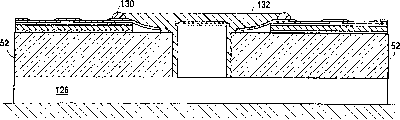
Fig. 3 illustrates the sectional view according to the design of the wafer-level package of an embodiment of institute's revealing method and device, between semiconductor die 52 and the intermediate circuit that comprises two-layer flex circuit band (or flexible circuit or TAB be with) 58 a non-polymer supporting structure 50 is set.In the present embodiment, non-polymer supporting structure 50 is by adhesive layer 64 and the coupling of matrix 52 implementation structures.Just as used herein, " structure coupling " mean utilize any suitable manner (as by deposit, adopt adhesive or other Type of Welding) make two elements directly coupling or indirect coupling (for example, use between the two insert layer or other element).As shown in Figure 3, semiconductor die 52 has matrix bonding pad or contact 84 usually.Second adhesive layer 56 is attached to flexibility with non-polymer liner 50 and is with on 58.Although Fig. 3 illustrates an embodiment of the wafer-level package design of adopting the two-layer flex circuit band, but, should be understood that the benefit of present disclosure is, adopt the intermediate circuit of other type, the inflexibility circuit band or the flexible circuit band that for example have three layers or multilayer also are fine.For example, Fig. 3 C illustrates and adopts three layers with 19 and an embodiment of wire bonds.In this embodiment, be with 19 to comprise dielectric layer 60, conductive layer 59 and second dielectric layer (being generally polyimides) 60a for three layers.Between layer 59 and 60a, adopt adhesive layer 60b.
Intermediate circuit generally includes the interconnection array that is connected with electricity such as the substrate of PCB.What in the embodiment shown in fig. 3, two-layer flex circuit band 58 generally included figuratum dielectric layer 60 and had each conductive bond pads 59a has a pattern plane conductive layer 59.Soldered ball conductive bond pads 59a general diameter is between 200 microns to 600 microns, and the spacing between the two is between 300 microns to 1250 microns.Can form by any electric conducting material that forms pattern of the circuit that is suitable for forming basic plane by pattern conductive layer 59, comprise such as silicon and polysilicon, tungsten, titanium, aluminium, based on the metal or the conductor of metal (as aluminium alloy), copper and the alloy and the combination etc. of aluminium, but be not limited thereto.(for present disclosure, term " metal " is defined as and comprises metal, refractory metal, interphase etc. and combination thereof).It is most typical that pattern conductive layer 59 is arranged is copper.Figuratum dielectric layer 60 can comprise polyimides or polyester, but be not limited thereto by being suitable for that any dielectric material that forms pattern of conductive layer 59 insulation is formed.Most typical dielectric layer 60 is polyimides, as " DUPONT KAPTON " or " UBE UPILEX ".The thickness of figuratum conductive layer 59 is usually between 0.5 mil to 1.5 mil.The thickness of figuratum dielectric layer 60 is usually between 1 mil to 3 mil.
In order to form ball grid array 57, conductive weld (or welding column) 54 be attached to flexibility with on 58 and the perforate (or through hole) 62 that forms by pattern in dielectric layer 60 contact with each welding gasket 59a electricity.Form perforate 62 patterns in mode, make each perforate cover each conductive bond pads 59a with each conductive bond pads 59a complementation.Soldered ball 54 can be to be adapted to pass through Any shape and the size that perforate 62 is connected with welding gasket 59a.Usually, soldered ball 54 is spherical substantially, and diameter is between 250 microns to 750 microns, and is the most frequently used between 300 microns to 600 microns.The traditional burner such as infrared, convection current or vapour phase of normally utilizing soldered ball refluxes fixing.Make the shape and size of perforate 62 be suitable for accepting soldered ball 54 by this way, promptly can with welding gasket 59a electricity contact mutually.Usually, perforate 62 is circular, and diameter is between 250 microns to 600 microns, and is the most frequently used between 300 microns to 500 microns.Conductive weld can be made of any suitable electric conducting material, comprises gold, solder flux or copper, but is not limited thereto.
In the embodiment shown in fig. 3, figuratum conductive layer 59 has a plurality of welding leads 82, each welding lead and conductive bond pads 59a electric coupling usually.Usually, the width of welding lead 82 is between 25 microns to 100 microns.Lead-in wire 82 is to be welded on the matrix liner 84 by for example lead to realize and being electrically connected of semiconductor die 52, and therefore disposes the spacing similar to matrix liner 84, length be enough to allow to go between 82 and liner 84 between pairing.Yet, also can go between 82, utilize the wire bonds 82a shown in Fig. 3 A to make liner 83 wire bonds on semiconductor die 52.In two kinds of situations, when each welding lead 82 is connected on each matrix 84 by electricity, between each soldered ball 54 and corresponding matrix liner 84, realize a circuit.When so constituting for the formation ball grid array, each soldered ball 54 of design is used as makes each " pin " that each matrix liner 84 is connected with corresponding welding gasket 75 electricity on the substrate 76.The spacing of ball grid array has corresponding substrate welding matrix liner 75, usually between 300 microns to 1250 microns as shown in Figure 6.Usually, substrate is printed circuit board (PCB) (" PCB "), but also can be any other circuit, comprises flexible circuit, silicon, substrate etc., but is not limited thereto.
As shown in Figure 3, sealed dose of 86 sealings usually of matrix 52 and lead bonding pad, sealant 86 is placed in the sealed enclosure 88.Sealant 86 can be any suitable sealant well-known to those skilled in the art, comprises epoxy resin and silicone, but is not limited thereto.Sealant capsule 88 can be any suitable sealant storage configuration, comprises for example epoxy resin, adhesive tape etc.Although embodiment shown in Figure 3 illustrates the wafer-level package design of adopting the figuratum conductive layer 59 of individual layer,, should be understood that benefit of the present invention is, embodiment also can adopt two-layer or multilayer that the conductive layer of pattern (or not having pattern) is arranged.
In the embodiments of figure 3, non-polymer liner 50 can be suitably firm so that handle and/or thermal coefficient of expansion approaches the substrate heat coefficient of expansion so that the stress on the pad reduces to minimum any material.Utilize such non-polymer gasket construction, can reduce or eliminate substantially in die attach adhesive 64 forming the space.This is because directly matrix 52 is welded on the non-polymer liner 60 with adhesive 64, therefore, does not have the moisture from polymeric material, and can not enter the interface between these two elements.
Except reducing thermal stress and space form, the non-polymer gasket construction of the method and apparatus that is disclosed also provides other significant advantage.For example, comprise the surface that the wafer-level package band of non-polymer supporting structure 10 provides, its evenness and surface uniformity increase than traditional elastic body liner.The evenness on grid matrix supporting structure surface is a key factor that guarantees that all soldered balls 54 contact with liner 75 on the substrate 76.More satisfactory ground, the coplanarity of wafer-level package supporting structure is about 2 mils or lower, more desirably, is about 1 mil or lower.This coplanarity adopts the traditional soft elastomer liner to be difficult to realize.The non-polymer supporting structure provides more flat surface for ball attach, therefore allow between semiconductor die and the substrate be connected more reliable.
Except above-mentioned benefit, can adopt thermal conducting non-polymer (is metal forming as sheet metal) as non-polymer supporting structure 50, for the heat dissipation of the front of semiconductor die from Fig. 3 52 back side of semiconductor die 52 (or among Fig. 3 A) provides good heat passage.This thermal conducting non-polymer supporting structure 50 can also be effectively heat conduction to soldered ball 54.
Usually one type the thermal conducting non-polymer that adopts is that sheet metal is a metal forming, and copper is the metal that is particularly suitable for this.Except thermal conductance, sheet metal can also improve the electric screen of conductive layer 59 and help to make cross (talk) to reduce to minimum.In addition, sheet metal provides the surface that is suitable for as ground plane.Therefore, sheet metal can also be used to provide a kind of ground plane easily (if necessary, or power planes), for example by soldered ball 54a directly is electrically connected with sheet metal 53, shown in Fig. 3 B.This can be for example adhesive phase 56 by through hole among the conductive gasket 59b 55 and below carry out, making selected ground connection connect soldered ball 54a can be electrically connected with sheet metal 53.Then, by lead or by wire bonds 82b the grounding gaskets in the matrix is connected with ground connection soldered ball 54a, shown in Fig. 3 B.Advantageously, when the sheet metal that adopts such as Copper Foil, can obtain these advantages with relatively low cost.Appropriate sheet of metal comprises any figuratum metal forming that enough hardness and/or thermal expansion quality are provided, comprise the metal forming of making by copper, stainless steel, alloy 42, tungsten, titanium, aluminium, based on metal (as aluminium alloy) and the alloy and the combination thereof etc. of aluminium, but be not limited thereto.Also can apply thin welding coating, good Weldability, low cost and/or reduction oxidation are provided to Copper Foil.The example of suitable coating comprises electronickelling, nickel/boron, black copper oxide, tin/the lead tin/lead alloy of the high lead content of 37% lead (as be higher than) or noble metal, as silver or golden overlay coating, but is not limited thereto.The most normally, the non-polymer supporting structure is the figuratum Copper Foil of thickness between 4 mil to 10 mils, and more normally, thickness is between 5 mil to 7 mils.Copper alloy as lead frame, as 194, is suitable for and should uses usually most.
When adopting the non-polymer liner of suitable stiffness, the typical chamber device for feeding process chip level encapsulation band commonly used with lead frame may be favourable." suitable hardness ", this is meant that modulus is greater than 1Mpsi (1 * 106 PSI).Example with non-polymer material of suitable stiffness comprises pottery and such as above-mentioned these metal forming.Yet, should be understood that the benefit of utilizing modulus also can realize institute's institute's revealing method and device less than the non-polymer of about 1Mpsi.These benefits comprise described these the benefit in other places in the literary composition.
With reference to figure 3, adhesive phase 56 and 64 can be fit to non-polymer liner 50 be fixed to flexibility with 58 and semiconductor die 52 on any adhesive.Usually, adhesive phase 56 and 64 is selected from dielectric material, dielectric material with non-polymer liner 50 effect be to have the matrix of making 52 and substrate (or PCB) 76 isolated or " uncoupling ", therefore further alleviate the stress on the pad and improve reliability.The also promising insertion socket of the effect of this adhesive provides a spot of Z axle compliance.The example of suitable bonding comprises " PYRALUX ", epoxy resin of acrylic acid PSA, thermoplastic polyimide (as " KJ " material of DuPont), polyolefin, DuPont company and composition thereof, but is not limited thereto.Usually adopt thermoplastic polyimide as adhesive phase 56 and 64.
Can as any thickness that forms welding between matrix or the circuit trace adhesive be put on the non-polymer liner with being suitable at elastomer liner and adjacently situated surfaces.Usually, adhesive phase 56 and 64 thickness are between 1 mil to 3 mil, and thickness more commonly used is between 1 mil to 2 mil.
Although the embodiment that illustrates adopts single non-polymer supporting structure,, should be appreciated that benefit of the present invention is, in chip stacked level packaging belt assembly, can adopt more than one non-polymer supporting structure.For example, can adopt the metal support structure of two or more electric isolation, use it for form to divide other circuit pathways (as ground plane and power planes the two), perhaps the combination of metal and nonmetal non-polymer supporting structure also is to be, as the glass epoxy printed board material.
In another embodiment shown in Fig. 3 D, mounting layer 351 can be copied the layer of deposit non-polymer material 350 and be used between semiconductor die 352 and the accessory circuit.For example, mounting layer 351 can be adhered on two-layer flex circuit band 318 or other intermediate circuit and with adhesive phase 364 with adhesive phase 356 and be adhered on the semiconductor circuit chip 352.When not being that the effect of non-polymer layer 350 is to escape into the formation that reduces or eliminate substantially the space in the die attach adhesive 364 by basic prevention moisture when adopting above-described non-polymer supporting structure embodiment.Can advantageously produce the mounting layer of copying the non-polymer material pattern in many ways, comprise as being with element separately or being attached to TAB and being with, but be not limited thereto.In some cases, utilize the mounting layer of copying the non-polymer material pattern may be cheaper than the embodiment of foregoing non-polymer supporting structure.
Still with reference to figure 3D, non-polymer layer 350 can be included as these materials of listing as the non-polymer supporting structure by being suitable for stoping moisture migration to be formed to any non-polymer material in the adhesive phase 364.Mounting layer 351 can be any material that is suitable for forming non-polymer layer 350 patterns or deposit, is included as these dielectric materials of listing as forming the dielectric material of pattern.Equally, adhesive phase 356 and 364 can be any suitable bonding or attachment means, is included as these that list for the non-polymer supporting structure uses.Common non-polymer layer 350 is thickness copper layers between 1 micron to 2 microns, and mounting layer 351 is thickness polyimide layers between 1 mil to 3 mil.More generally, non-polymer layer 350 is thickness copper layers between 5 microns to 10 microns, and mounting layer 351 is polyimide layers that thickness is about 2 mils.
Fig. 3 D is illustrated in to be similar to and has used the mounting layer 351 of copying non-polymer layer 350 in the application shown in Fig. 3 A.The same with the embodiment of non-polymer supporting structure, can make many variations for the structure shown in Fig. 3 D.For example, conduction non-polymer layer 350 can be used as ground plane, power planes or finish the circuit pathways of other type, as being the shown mode of non-polymer supporting structure to be similar to Fig. 3 B.Mounting layer 351 and non-polymer layer 351 also can use with having three layers or more multi-layered intermediate circuit, as being that the shown embodiment of non-polymer supporting structure is similar to Fig. 3 C.In addition, can adopt more than one non-polymer layer 350.
The manufacturing of wafer-level package element and assembling
Can form the wafer-level package device of disclosed method and apparatus in many ways, and use it in many different application with non-polymer supporting structure (or " liner ").For example, a kind of method that structure has the wafer-level package band of non-polymer liner comprises step: adhesive is folded on the cylinder of non-polymer material (as metal forming), with required form punching press or mold pressing non-polymer material, crooked circuit (or circuit trace) is aimed at non-polymer and bonding, formed the wafer-level package band form of band (for example with).In another diverse ways, by non-polymer material (figure metal forming) is struck out required form, adhesive films is struck out identical shape, the two is aimed at the circuit trace to make film and paillon foil, and make structure superposition, can form the wafer-level package band.In both of these case, the circuit trace is accurately with aiming at of non-polymer supporting structure, also is cheaper.Can carry out multiple different step, utilize described just now wafer-level package band or band to form the wafer-level package device.These steps comprise: die attach, lead-in wire and/or lead weld, cross mold and/or ball attach step.Advantageously, the assembling according to the wafer-level package device of these processes is more effective, direct and cost-effective.
Fig. 4 illustrates the both sides that adhesive phase 56 and 64 is folded into the thin reel of copper sheet (or paper tinsel) 50.Usually, adopt to have the adhesive laminate of cover layer (or release liner), release liner is left on adhesive phase 56 and 64 to deviate from this side of Copper Foil 50.The adhesive laminate that adds release liner comprises acrylic acid PSA type adhesive.As shown in Figure 4, the superimposed adhesive that is used to form adhesive phase 56 and 64 normally utilizes cylinder lamination 100 to apply.Yet, should be understood that benefit of the present invention is, can utilize any suitable method, include, but is not limited to silk screen printing and spray sedimentation, apply such as foregoing these adhesives.
Fig. 5 illustrates the vertical view of the non-polymer sheet 50 that is superimposed together with adhesive phase 56 and 64.In Fig. 5,50 punching presses of non-polymer sheet or mold pressing have been formed have be connected groove zone 110 around the pattern of matrix square 51.Matrix square 51 is constructed with and complementary mutually shape of semiconductor die 52 and littler area, and the matrix liner 84 of being connected in the link slot zone 110 for 82 (the perhaps wire bonds) that go between leaves the gap.Link slot 110 provides the space for utilizing lead welding, wire bonds or other suitable method of attachment to be connected on the matrix liner 84.Altogether, matrix square 51 and link slot 110 are of a size of semiconductor die 52 each platform are provided.
Should be appreciated that benefit of the present invention is, mold pressing or punching operation can utilize any any punching press or mould pressing method that is suitable for the integrated circuit encapsulation to carry out in the method that is disclosed.By chemical etching, utilize the steel ruler matrix or utilize the chemical etching matrix also can make non-polymer form pattern.Also can stamping tool hole 112 in sheet 50, help the accurate aligning of circuit.
Then, as shown in Figure 6, utilize tooling hole 112 to make to have the flexibility of the through hole 62 of accepting soldered ball to aim at and be folded on the side of copper sheet 50 with 58.The superimposed of circuit can carry out in many ways, comprises with cylinder-cylinder method (as cylinder-cylinder method of utilizing sprocket hole) or with method for stamping.In the present embodiment, before superimposed, tear release liner off usually, utilize, the panel or the band of circuit is folded on the sheet 50 mutatis mutandis tooling hole from adhesive phase 56.Yet, can adopt other bonding and folding method, method as previously described.
At this moment, the adhering to and weld and can interruptedly not continue of integrated circuit, the flexibility that is attached is with 58 can be sent to other places, for further assembling.In the later case, before conveying, be with 58 to cut into strips non-polymer sheet 50 and the flexibility of adhering to usually.Use strips, single wafer-level package band has several usually and divides other matrix square 51.In both of these case, further assembling is usually directed to remove second release liner from adhesive phase 64, prepares for matrix is installed on the non-polymer sheet 50.In the situation of strips technology, the band of non-polymer sheet and the circuit that adheres to are loaded in the hopper of handling usefulness.Then matrix is placed on the viscosity side (relative) of non-polymer band, makes it if necessary to solidify with the side that circuit is arranged.Yet, should be understood that benefit of the present invention is, matrix also can tested and is placed on the volume non-polymer sheet (relative with band), and semiconductor die can be placed with its circuit, and is adjacent with the non-polymer sheet or relative.Also can make the matrix side of non-polymer band stay exposed adhesive and die attach adhesive (being generally material), for the use of adhering to of matrix based on epoxy resin.
Then, make band (comprising circuit and one or more matrix) upside-down mounting and be placed in the standard hopper, it for example is loaded in lead welding machine or the thermocompression bonder.As shown in Figure 7, each lead-in wire 120 that utilizes soldering appliance for example 124 to carry in the future is welded on the matrix liner 122.Utilize the fixture 126 flexible bands of supporting (comprising matrix), thereby lead-in wire 120 is ruptured in frangible part (or indentation) 126 during welding process.As shown in Figure 8, then, by making band cross mold with sealant 132 filling slots 110.Usually, sealant is blocked parts 130 and contains, and utilizes suitable curing, is cured as ultraviolet or by the use of thermal means.Perhaps, as shown in Figure 9, can with the band upside-down mounting on fixture surface 140,, need not the sealant stop member with the matrix one side filling slot 110 of sealant 132 from band.Shown in Fig. 3 A and 3B, matrix 52 also can utilize wire bonds 82a to be connected on the circuit trace layer 59, for example, when semiconductor die is " flip-chip ", makes the matrix liner of circuit layer and semiconductor die be oriented to the direction that deviates from supporting structure.Fig. 6 A illustrates the vertical view of this embodiment.
As shown in figure 10, then soldered ball (or welding column) 54 can be contained in the perforate (or through hole) 62 of formation, for example in the perforate by etching in polyimide layer 60.Utilization is suitable for forming any method that firm electricity is connected between ball 54 and conductive solder liner 59a, comprises that any traditional means of for example utilizing such as infrared, convection current or vapour phase heats and refluxes, and can make soldered ball 54 be attached on the band.Although it is not shown,, through hole 62 also can be treated to electroplating ventilating hole (PTH) and/or fill different conductive fill agent materials before ball attach.
At this moment, can cut, form the wafer-level package (Figure 10 illustrates the encapsulation 150 of a single matrix) of single or multiple matrixs band or reel.This can utilize such as any suitable cutting method of punching press, cutting or other similar procedure and finish.
Should be understood that benefit of the present invention is, utilize this method, can prepare the structure of other wafer-level package, comprise encapsulation with an above semiconductor die.In addition, utilize disclosed method and apparatus notion can make the structure of the non-wafer-level package that encapsulates such as traditional B GA.Be to be further appreciated that, though the method for describing and illustrating just now is to make integrated circuit in order to utilize band to form, but, when being used to utilize other process and form to make integrated circuit, comprise and utilize cylinder-cylinder (perhaps reel-reel) form to form integrated circuit, but be not limited thereto, also can obtain the benefit of these methods.In this respect, with the compatible mutually form of existing industrial foundation structure with use the form of the current renewal that is developed to realize the benefit of institute's institute's revealing method and device.Be to be further appreciated that above-mentioned encapsulation process can be carried out with the matrix in the substrate form still.For example, can make the non-polymer sheet aim at and be directly bonded on the substrate and chip that welds.As previously mentioned, use the sealant filling slot then, adhere to soldered ball and punching press or cut each packaging part.
The present invention can be suitable for various improvement and version,, has illustrated and described specific embodiment by way of example here.Yet, should be understood that and not wish that the present invention is limited to disclosed concrete form.But the present invention's covering drops on the interior all improvement of the spirit and scope of the present invention defined in the appended claims.Equivalence and alternative.
Claims (32)
1. the encapsulation of an integrated circuit is characterized in that it comprises:
The intermediate circuit that comprises the electronic interconnection array;
The non-polymer layer of one deck at least with first and second sides, first side of described layer and the coupling of described integrated circuit phase structure, second side of described layer and the coupling of described intermediate circuit phase structure.
2. encapsulation as claimed in claim 1 is characterized in that: described integrated circuit has a plurality of electric contact points, and the described electrical interconnection of described contact site and described intermediate circuit is electrical couplings mutually.
3. encapsulation as claimed in claim 2 is characterized in that: the described electric contact points of described integrated circuit by wire bonds on the described electrical interconnection of described intermediate circuit.
4. encapsulation as claimed in claim 2 is characterized in that: the described electric contact points of described integrated circuit is received on the described electrical interconnection of described intermediate circuit by thermocompression bonding.
5. encapsulation as claimed in claim 1 is characterized in that: described non-polymer layer conducts electricity, and described non-polymer layer is electrically coupled on the described integrated circuit, forms power supply or ground plane.
6. encapsulation as claimed in claim 1 is characterized in that: described non-polymer layer is the non-polymer supporting structure of modulus greater than about 1Mpsi.
7. encapsulation as claimed in claim 1 is characterized in that: the non-polymer supporting structure that described non-polymer layer is made up of the metal forming of thickness between 4 mil to 10 mils.
8. encapsulation as claimed in claim 1 is characterized in that: the non-polymer supporting structure that described non-polymer layer is made up of Copper Foil.
9. encapsulation as claimed in claim 1, it is characterized in that further comprising mounting layer with first and second sides, second side phase structure coupling, second side of described mounting layer and the coupling of described intermediate circuit phase structure of first side of described mounting layer and described non-polymer layer.
10. encapsulation as claimed in claim 9 is characterized in that: described mounting layer is the polyimide layer of thickness between 1 mil to 3 mil, and described non-polymer layer is the copper layer of thickness between 1 micron to 20 microns.
11. encapsulation as claimed in claim 1 is characterized in that: described intermediate circuit is a flexible circuit.
12. encapsulation as claimed in claim 1 is characterized in that: described intermediate circuit has first and second sides, the second side phase structure coupling of first side of described intermediate circuit and described non-polymer layer; With
Further comprise a plurality of and described the intermediate circuit soldered ball or the welding column of electrical couplings mutually; The second side phase structure coupling of described a plurality of soldered ball or welding column and described intermediate circuit.
13. a method that forms the integrated circuit encapsulation is characterized in that described method comprises step:
One intermediate circuit that comprises the electricity interlinkage array is provided;
One deck at least with first and second sides non-polymer layer is provided; First side of described non-polymer layer is suitable for and described integrated circuit phase structure coupling; With
Second side structure of described non-polymer layer is coupled on the described intermediate circuit.
14. method as claimed in claim 13 is characterized in that further comprising described integrated circuit structurally is coupled to step on described first side of described non-polymer layer.
15. method as claimed in claim 14 is characterized in that: described integrated circuit has a plurality of electric contact points, further comprises described contact site in the step that is coupled on the electricity on the described electricity interlinkage of described intermediate circuit.
16. method as claimed in claim 14 is characterized in that: described contact site electricity is coupled to step on the described electricity interlinkage comprises step on the described electricity interlinkage of described intermediate circuit is received in the described contact site wire bonds of described integrated circuit or thermocompression bonding.
17. method as claimed in claim 14 is characterized in that: described non-polymer layer conducts electricity, and further comprises described non-polymer supporting structure is electrically coupled on the described integrated circuit, forms the step of power supply and ground plane.
18. method as claimed in claim 13 is characterized in that: described non-polymer layer is the non-polymer supporting structure of modulus greater than about 1Mpsi.
19. method as claimed in claim 13 is characterized in that: described non-polymer layer is non-polymeric support structure, is the metal forming of thickness between 4 mil to 10 mils.
20. method as claimed in claim 13 is characterized in that: described non-polymer layer is the non-polymer supporting structure that comprises Copper Foil.
21. method as claimed in claim 13 is characterized in that: described non-polymer layer is the copper layer of thickness between 1 micron to 20 microns.
22. method as claimed in claim 13 is characterized in that: described intermediate circuit is a flexible circuit.
23. method as claimed in claim 13 is characterized in that: described intermediate circuit has first and second sides; The described step that described intermediate circuit structure is coupled to described non-polymer layer comprises the step that first side of described intermediate circuit structurally is connected to second side of described non-polymer layer; Further comprise the step that a plurality of soldered balls or welding column is electrically coupled to described intermediate circuit; Described a plurality of soldered ball or welding column are coupled to described second side of described intermediate circuit by structure.
24. an Electronic Packaging is characterized in that it comprises:
Comprise the figuratum conductive layer of one deck and the flexibility band of the figuratum dielectric layer of one deck at least;
Non-polymer supporting structure with first and second sides, first side of described supporting structure is coupled on second side of the described flexible described conductive layer of being with by structure.
25. encapsulation as claimed in claim 24, it is characterized in that: described conductive layer has first and second sides and impressing pattern to form conductive region, described dielectric layer has first and second sides and carries out pattern and handle a plurality of perforates of passing described dielectric layer extension with formation, in the described perforate each is configured to receive a soldered ball, first side of conductive layer described here is connected to second side of described dielectric layer, thereby makes aligning to the described conductive region of small part of described a plurality of perforates in the described dielectric layer and described conductive layer.
26. encapsulation as claimed in claim 25, it is characterized in that further comprising that its first side is coupled to the semiconductor device of second side of described non-polymer supporting structure by structure, described semiconductor device comprises a plurality of electric contact points, and described contact site is electrically coupled on the described conductive layer of described flexible band.
27. encapsulation as claimed in claim 26, it is characterized in that further comprising a plurality of soldered balls or welding column on first side of the described dielectric layer that is arranged on described flexible band, each in described soldered ball or the welding column is positioned in the perforate of a plurality of perforates described in the described dielectric layer and is electrically connected on the described conduction region of described conductive layer of described flexible band.
28. encapsulation as claimed in claim 27 is characterized in that: the modulus of described non-polymer supporting structure is greater than about 1Mpsi.
29. encapsulation as claimed in claim 27 is characterized in that: described non-polymer supporting structure is the Copper Foil of thickness between 4 mil to 10 mils.
30. an Electronic Packaging is characterized in that it comprises:
What have first and second sides and an outer boundaries has a pattern conductive layer, and described conductive layer is carried out patterning to form the conductive region that peripheral conductive features is set around the circumference of described outer boundaries, as the electrical connection of semiconductor device;
Have first and second sides and circumference and the pattern dielectric layer arranged less than the outer boundaries of the described described circumference that the pattern conductive layer arranged, described dielectric layer is carried out patterning pass a plurality of perforates that described dielectric layer extends with formation, each perforate in the described perforate is set to receive a soldered ball, here, first side of described conductive layer is connected to second side of described dielectric layer, so that the aligning to the described conductive region of small part of described a plurality of perforates in the described dielectric layer and described conductive layer, the described peripheral conductive features of described conductive layer extends to beyond the outer boundaries of described dielectric member;
Non-polymer supporting structure with first and second sides, described supporting structure are firm substantially and have modulus of elasticity greater than about 1Mpsi that first side of described supporting structure is coupled on second side of described conductive layer by structure;
Semiconductor device with first side, described first side is coupled on second side of described non-polymer supporting structure by structure, described semiconductor device comprises a plurality of electric contact points, has at least in the described contact site on the described peripheral conductive features that is electrically coupled to described conductive layer; And
Be arranged on a plurality of soldered balls on first side of described dielectric layer, each in the described soldered ball is positioned in the perforate of a plurality of perforates described in the described dielectric layer and is electrically connected on the described conduction region of described conductive layer.
31. encapsulation as claimed in claim 30 is characterized in that: the described electric contact points of described semiconductor device is to adopt the means of wire bonds, lead or its combination to be electrically coupled on the described peripheral conductive features of described conductive layer.
32. encapsulation as claimed in claim 30, it is characterized in that: described non-polymer supporting structure conducts electricity, described non-polymer supporting structure between at least one position and the described conductive layer, is made described non-polymer supporting structure form electric circuit between described semiconductor device and described conductive layer by electric coupling in the described electric contact points of described semiconductor device.
Applications Claiming Priority (2)
| Application Number | Priority Date | Filing Date | Title |
|---|---|---|---|
| US08/759,253 | 1996-12-02 | ||
| US08/759,253 US5990545A (en) | 1996-12-02 | 1996-12-02 | Chip scale ball grid array for integrated circuit package |
Publications (1)
| Publication Number | Publication Date |
|---|---|
| CN1239589A true CN1239589A (en) | 1999-12-22 |
Family
ID=25054972
Family Applications (1)
| Application Number | Title | Priority Date | Filing Date |
|---|---|---|---|
| CN97180210A Pending CN1239589A (en) | 1996-12-02 | 1997-04-02 | Chip scale ball grid array for intergrated circuit package |
Country Status (12)
| Country | Link |
|---|---|
| US (1) | US5990545A (en) |
| EP (1) | EP0948814B1 (en) |
| JP (1) | JP2001506057A (en) |
| KR (1) | KR100532179B1 (en) |
| CN (1) | CN1239589A (en) |
| AT (1) | ATE273564T1 (en) |
| AU (1) | AU2435397A (en) |
| CA (1) | CA2272434A1 (en) |
| DE (1) | DE69730239D1 (en) |
| HK (1) | HK1023225A1 (en) |
| MY (1) | MY119341A (en) |
| WO (1) | WO1998025303A1 (en) |
Cited By (2)
| Publication number | Priority date | Publication date | Assignee | Title |
|---|---|---|---|---|
| CN108122873A (en) * | 2016-11-28 | 2018-06-05 | 日月光半导体制造股份有限公司 | The semiconductor packages of connection column are moulded including filling |
| CN112180128A (en) * | 2020-09-29 | 2021-01-05 | 西安微电子技术研究所 | Interconnection substrate with elastic conductive micro-bumps and KGD socket based on interconnection substrate |
Families Citing this family (89)
| Publication number | Priority date | Publication date | Assignee | Title |
|---|---|---|---|---|
| JP2891665B2 (en) | 1996-03-22 | 1999-05-17 | 株式会社日立製作所 | Semiconductor integrated circuit device and method of manufacturing the same |
| US20040061220A1 (en) * | 1996-03-22 | 2004-04-01 | Chuichi Miyazaki | Semiconductor device and manufacturing method thereof |
| JP3195236B2 (en) | 1996-05-30 | 2001-08-06 | 株式会社日立製作所 | Wiring tape having adhesive film, semiconductor device and manufacturing method |
| US6962829B2 (en) * | 1996-10-31 | 2005-11-08 | Amkor Technology, Inc. | Method of making near chip size integrated circuit package |
| US6150193A (en) * | 1996-10-31 | 2000-11-21 | Amkor Technology, Inc. | RF shielded device |
| US5981314A (en) | 1996-10-31 | 1999-11-09 | Amkor Technology, Inc. | Near chip size integrated circuit package |
| DE69830883T2 (en) * | 1997-03-10 | 2006-04-20 | Seiko Epson Corp. | Semiconductor device and equipped with this device circuit board |
| JP3301355B2 (en) * | 1997-07-30 | 2002-07-15 | 日立電線株式会社 | Semiconductor device, TAB tape for semiconductor device, method of manufacturing the same, and method of manufacturing semiconductor device |
| US5888850A (en) * | 1997-09-29 | 1999-03-30 | International Business Machines Corporation | Method for providing a protective coating and electronic package utilizing same |
| US6310298B1 (en) * | 1997-12-30 | 2001-10-30 | Intel Corporation | Printed circuit board substrate having solder mask-free edges |
| US6574858B1 (en) | 1998-02-13 | 2003-06-10 | Micron Technology, Inc. | Method of manufacturing a chip package |
| JP3481117B2 (en) * | 1998-02-25 | 2003-12-22 | 富士通株式会社 | Semiconductor device and manufacturing method thereof |
| US6166433A (en) * | 1998-03-26 | 2000-12-26 | Fujitsu Limited | Resin molded semiconductor device and method of manufacturing semiconductor package |
| US6265776B1 (en) * | 1998-04-27 | 2001-07-24 | Fry's Metals, Inc. | Flip chip with integrated flux and underfill |
| US6089920A (en) * | 1998-05-04 | 2000-07-18 | Micron Technology, Inc. | Modular die sockets with flexible interconnects for packaging bare semiconductor die |
| WO2000005765A1 (en) * | 1998-07-22 | 2000-02-03 | Dyconex Patente Ag | Method for producing rewiring substrates for semiconductor chip packages |
| US6479887B1 (en) | 1998-08-31 | 2002-11-12 | Amkor Technology, Inc. | Circuit pattern tape for wafer-scale production of chip size semiconductor packages |
| US6428641B1 (en) | 1998-08-31 | 2002-08-06 | Amkor Technology, Inc. | Method for laminating circuit pattern tape on semiconductor wafer |
| KR20010099684A (en) | 1998-10-14 | 2001-11-09 | 스프레이그 로버트 월터 | Tape ball grid array with interconnected ground plane |
| JP2000138317A (en) | 1998-10-31 | 2000-05-16 | Anam Semiconductor Inc | Semiconductor device and its manufacture |
| JP2000138262A (en) | 1998-10-31 | 2000-05-16 | Anam Semiconductor Inc | Chip-scale semiconductor package and manufacture thereof |
| TW434850B (en) * | 1998-12-31 | 2001-05-16 | World Wiser Electronics Inc | Packaging equipment and method for integrated circuit |
| US6175160B1 (en) * | 1999-01-08 | 2001-01-16 | Intel Corporation | Flip-chip having an on-chip cache memory |
| US6377464B1 (en) * | 1999-01-29 | 2002-04-23 | Conexant Systems, Inc. | Multiple chip module with integrated RF capabilities |
| US6341418B1 (en) | 1999-04-29 | 2002-01-29 | International Business Machines Corporation | Method for direct chip attach by solder bumps and an underfill layer |
| US6191483B1 (en) * | 1999-05-06 | 2001-02-20 | Philips Electronics North America Corporation | Package structure for low cost and ultra thin chip scale package |
| JP3397725B2 (en) * | 1999-07-07 | 2003-04-21 | 沖電気工業株式会社 | Semiconductor device, manufacturing method thereof, and manufacturing method of semiconductor device mounting tape |
| JP3521325B2 (en) * | 1999-07-30 | 2004-04-19 | シャープ株式会社 | Manufacturing method of resin-encapsulated semiconductor device |
| US6285077B1 (en) * | 1999-08-19 | 2001-09-04 | Lsi Logic Corporation | Multiple layer tape ball grid array package |
| JP2001156212A (en) * | 1999-09-16 | 2001-06-08 | Nec Corp | Resin sealed semiconductor device and producing method therefor |
| US6656765B1 (en) | 2000-02-02 | 2003-12-02 | Amkor Technology, Inc. | Fabricating very thin chip size semiconductor packages |
| US6560108B2 (en) * | 2000-02-16 | 2003-05-06 | Hughes Electronics Corporation | Chip scale packaging on CTE matched printed wiring boards |
| US6686652B1 (en) | 2000-03-20 | 2004-02-03 | National Semiconductor | Locking lead tips and die attach pad for a leadless package apparatus and method |
| US6452255B1 (en) | 2000-03-20 | 2002-09-17 | National Semiconductor, Corp. | Low inductance leadless package |
| US6372539B1 (en) | 2000-03-20 | 2002-04-16 | National Semiconductor Corporation | Leadless packaging process using a conductive substrate |
| US6399415B1 (en) * | 2000-03-20 | 2002-06-04 | National Semiconductor Corporation | Electrical isolation in panels of leadless IC packages |
| DE10014380A1 (en) * | 2000-03-23 | 2001-10-04 | Infineon Technologies Ag | Device for packaging electronic components |
| US6444499B1 (en) * | 2000-03-30 | 2002-09-03 | Amkor Technology, Inc. | Method for fabricating a snapable multi-package array substrate, snapable multi-package array and snapable packaged electronic components |
| US6320137B1 (en) * | 2000-04-11 | 2001-11-20 | 3M Innovative Properties Company | Flexible circuit with coverplate layer and overlapping protective layer |
| TW466720B (en) * | 2000-05-22 | 2001-12-01 | Siliconware Precision Industries Co Ltd | Semiconductor package with flash-prevention structure and manufacture method |
| US6501170B1 (en) | 2000-06-09 | 2002-12-31 | Micron Technology, Inc. | Substrates and assemblies including pre-applied adhesion promoter |
| US6710456B1 (en) * | 2000-08-31 | 2004-03-23 | Micron Technology, Inc. | Composite interposer for BGA packages |
| JP4570809B2 (en) * | 2000-09-04 | 2010-10-27 | 富士通セミコンダクター株式会社 | Multilayer semiconductor device and manufacturing method thereof |
| US6624005B1 (en) | 2000-09-06 | 2003-09-23 | Amkor Technology, Inc. | Semiconductor memory cards and method of making same |
| US6809935B1 (en) | 2000-10-10 | 2004-10-26 | Megic Corporation | Thermally compliant PCB substrate for the application of chip scale packages |
| US6552436B2 (en) * | 2000-12-08 | 2003-04-22 | Motorola, Inc. | Semiconductor device having a ball grid array and method therefor |
| DE10064691A1 (en) * | 2000-12-22 | 2002-07-04 | Infineon Technologies Ag | Electronic component comprises a semiconductor chip with copper conducting pathways for connecting semiconductor electrode surfaces of elements of the chip to copper contact surfaces |
| US6770963B1 (en) | 2001-01-04 | 2004-08-03 | Broadcom Corporation | Multi-power ring chip scale package for system level integration |
| DE10120408B4 (en) * | 2001-04-25 | 2006-02-02 | Infineon Technologies Ag | Electronic component with a semiconductor chip, electronic assembly of stacked semiconductor chips and method for their production |
| US7115986B2 (en) | 2001-05-02 | 2006-10-03 | Micron Technology, Inc. | Flexible ball grid array chip scale packages |
| EP1280204A3 (en) * | 2001-06-27 | 2004-09-01 | Shinko Electric Industries Co. Ltd. | Wiring substrate having position problem |
| US6793759B2 (en) * | 2001-10-09 | 2004-09-21 | Dow Corning Corporation | Method for creating adhesion during fabrication of electronic devices |
| US6873059B2 (en) * | 2001-11-13 | 2005-03-29 | Texas Instruments Incorporated | Semiconductor package with metal foil attachment film |
| US6664615B1 (en) * | 2001-11-20 | 2003-12-16 | National Semiconductor Corporation | Method and apparatus for lead-frame based grid array IC packaging |
| US6657134B2 (en) | 2001-11-30 | 2003-12-02 | Honeywell International Inc. | Stacked ball grid array |
| SG104291A1 (en) * | 2001-12-08 | 2004-06-21 | Micron Technology Inc | Die package |
| SG104293A1 (en) | 2002-01-09 | 2004-06-21 | Micron Technology Inc | Elimination of rdl using tape base flip chip on flex for die stacking |
| SG115455A1 (en) | 2002-03-04 | 2005-10-28 | Micron Technology Inc | Methods for assembly and packaging of flip chip configured dice with interposer |
| SG111935A1 (en) * | 2002-03-04 | 2005-06-29 | Micron Technology Inc | Interposer configured to reduce the profiles of semiconductor device assemblies and packages including the same and methods |
| SG115456A1 (en) | 2002-03-04 | 2005-10-28 | Micron Technology Inc | Semiconductor die packages with recessed interconnecting structures and methods for assembling the same |
| SG121707A1 (en) | 2002-03-04 | 2006-05-26 | Micron Technology Inc | Method and apparatus for flip-chip packaging providing testing capability |
| US6975035B2 (en) | 2002-03-04 | 2005-12-13 | Micron Technology, Inc. | Method and apparatus for dielectric filling of flip chip on interposer assembly |
| SG115459A1 (en) | 2002-03-04 | 2005-10-28 | Micron Technology Inc | Flip chip packaging using recessed interposer terminals |
| US7132173B2 (en) * | 2002-06-28 | 2006-11-07 | Advanced Bionics Corporation | Self-centering braze assembly |
| US20040036170A1 (en) | 2002-08-20 | 2004-02-26 | Lee Teck Kheng | Double bumping of flexible substrate for first and second level interconnects |
| US6921975B2 (en) * | 2003-04-18 | 2005-07-26 | Freescale Semiconductor, Inc. | Circuit device with at least partial packaging, exposed active surface and a voltage reference plane |
| US7266869B2 (en) * | 2003-07-30 | 2007-09-11 | Kyocera Corporation | Method for manufacturing a piezoelectric oscillator |
| US20050056946A1 (en) * | 2003-09-16 | 2005-03-17 | Cookson Electronics, Inc. | Electrical circuit assembly with improved shock resistance |
| JP3929966B2 (en) * | 2003-11-25 | 2007-06-13 | 新光電気工業株式会社 | Semiconductor device and manufacturing method thereof |
| US7075016B2 (en) * | 2004-02-18 | 2006-07-11 | Taiwan Semiconductor Manufacturing Co., Ltd. | Underfilling efficiency by modifying the substrate design of flip chips |
| US11081370B2 (en) * | 2004-03-23 | 2021-08-03 | Amkor Technology Singapore Holding Pte. Ltd. | Methods of manufacturing an encapsulated semiconductor device |
| DE102004020580A1 (en) * | 2004-04-27 | 2005-11-17 | Infineon Technologies Ag | Method of manufacturing a BGA chip module and BGA chip module |
| US7071559B2 (en) * | 2004-07-16 | 2006-07-04 | International Business Machines Corporation | Design of beol patterns to reduce the stresses on structures below chip bondpads |
| US8125076B2 (en) * | 2004-11-12 | 2012-02-28 | Stats Chippac Ltd. | Semiconductor package system with substrate heat sink |
| JP4343117B2 (en) * | 2005-01-07 | 2009-10-14 | 株式会社ルネサステクノロジ | Semiconductor device and manufacturing method thereof |
| US7968371B2 (en) * | 2005-02-01 | 2011-06-28 | Stats Chippac Ltd. | Semiconductor package system with cavity substrate |
| US7316572B2 (en) * | 2005-02-03 | 2008-01-08 | International Business Machines Corporation | Compliant electrical contacts |
| US20070018308A1 (en) * | 2005-04-27 | 2007-01-25 | Albert Schott | Electronic component and electronic configuration |
| JP4548264B2 (en) * | 2005-08-01 | 2010-09-22 | 株式会社デンソー | Vehicle alternator |
| DE102006015222B4 (en) * | 2006-03-30 | 2018-01-04 | Robert Bosch Gmbh | QFN package with optimized pad geometry |
| US7788960B2 (en) * | 2006-10-27 | 2010-09-07 | Cummins Filtration Ip, Inc. | Multi-walled tube and method of manufacture |
| US7573131B2 (en) * | 2006-10-27 | 2009-08-11 | Compass Technology Co., Ltd. | Die-up integrated circuit package with grounded stiffener |
| TWI352406B (en) * | 2006-11-16 | 2011-11-11 | Nan Ya Printed Circuit Board Corp | Embedded chip package with improved heat dissipati |
| US7944029B2 (en) * | 2009-09-16 | 2011-05-17 | Sandisk Corporation | Non-volatile memory with reduced mobile ion diffusion |
| JP5642473B2 (en) * | 2010-09-22 | 2014-12-17 | セイコーインスツル株式会社 | BGA semiconductor package and manufacturing method thereof |
| US9159649B2 (en) * | 2011-12-20 | 2015-10-13 | Intel Corporation | Microelectronic package and stacked microelectronic assembly and computing system containing same |
| TWI544583B (en) * | 2012-04-18 | 2016-08-01 | 鴻海精密工業股份有限公司 | Chip assembly and chip assembling method |
| TWI480989B (en) | 2012-10-02 | 2015-04-11 | 矽品精密工業股份有限公司 | Semiconductor package and fabrication method thereof |
| US20160317068A1 (en) * | 2015-04-30 | 2016-11-03 | Verily Life Sciences Llc | Electronic devices with encapsulating silicone based adhesive |
Family Cites Families (22)
| Publication number | Priority date | Publication date | Assignee | Title |
|---|---|---|---|---|
| FR2439478A1 (en) * | 1978-10-19 | 1980-05-16 | Cii Honeywell Bull | FLAT HOUSING FOR DEVICES WITH INTEGRATED CIRCUITS |
| US5148265A (en) * | 1990-09-24 | 1992-09-15 | Ist Associates, Inc. | Semiconductor chip assemblies with fan-in leads |
| US5148266A (en) * | 1990-09-24 | 1992-09-15 | Ist Associates, Inc. | Semiconductor chip assemblies having interposer and flexible lead |
| US5216278A (en) * | 1990-12-04 | 1993-06-01 | Motorola, Inc. | Semiconductor device having a pad array carrier package |
| US5241133A (en) * | 1990-12-21 | 1993-08-31 | Motorola, Inc. | Leadless pad array chip carrier |
| JPH05160292A (en) * | 1991-06-06 | 1993-06-25 | Toshiba Corp | Multilayer package |
| US5311059A (en) * | 1992-01-24 | 1994-05-10 | Motorola, Inc. | Backplane grounding for flip-chip integrated circuit |
| US5214845A (en) * | 1992-05-11 | 1993-06-01 | Micron Technology, Inc. | Method for producing high speed integrated circuits |
| US5592025A (en) * | 1992-08-06 | 1997-01-07 | Motorola, Inc. | Pad array semiconductor device |
| US5468994A (en) * | 1992-12-10 | 1995-11-21 | Hewlett-Packard Company | High pin count package for semiconductor device |
| US5420460A (en) * | 1993-08-05 | 1995-05-30 | Vlsi Technology, Inc. | Thin cavity down ball grid array package based on wirebond technology |
| US5397921A (en) * | 1993-09-03 | 1995-03-14 | Advanced Semiconductor Assembly Technology | Tab grid array |
| US5477611A (en) * | 1993-09-20 | 1995-12-26 | Tessera, Inc. | Method of forming interface between die and chip carrier |
| US5548091A (en) * | 1993-10-26 | 1996-08-20 | Tessera, Inc. | Semiconductor chip connection components with adhesives and methods for bonding to the chip |
| US5473512A (en) * | 1993-12-16 | 1995-12-05 | At&T Corp. | Electronic device package having electronic device boonded, at a localized region thereof, to circuit board |
| TW258829B (en) * | 1994-01-28 | 1995-10-01 | Ibm | |
| EP0751561A4 (en) * | 1994-03-18 | 1997-05-07 | Hitachi Chemical Co Ltd | Semiconductor package manufacturing method and semiconductor package |
| US5741729A (en) * | 1994-07-11 | 1998-04-21 | Sun Microsystems, Inc. | Ball grid array package for an integrated circuit |
| JP2616565B2 (en) * | 1994-09-12 | 1997-06-04 | 日本電気株式会社 | Electronic component assembly |
| US5528083A (en) * | 1994-10-04 | 1996-06-18 | Sun Microsystems, Inc. | Thin film chip capacitor for electrical noise reduction in integrated circuits |
| JP3123638B2 (en) * | 1995-09-25 | 2001-01-15 | 株式会社三井ハイテック | Semiconductor device |
| US5674785A (en) * | 1995-11-27 | 1997-10-07 | Micron Technology, Inc. | Method of producing a single piece package for semiconductor die |
-
1996
- 1996-12-02 US US08/759,253 patent/US5990545A/en not_active Expired - Fee Related
-
1997
- 1997-04-02 WO PCT/US1997/005489 patent/WO1998025303A1/en active IP Right Grant
- 1997-04-02 AU AU24353/97A patent/AU2435397A/en not_active Abandoned
- 1997-04-02 DE DE69730239T patent/DE69730239D1/en not_active Expired - Lifetime
- 1997-04-02 EP EP97920070A patent/EP0948814B1/en not_active Expired - Lifetime
- 1997-04-02 JP JP52554098A patent/JP2001506057A/en active Pending
- 1997-04-02 CN CN97180210A patent/CN1239589A/en active Pending
- 1997-04-02 CA CA002272434A patent/CA2272434A1/en not_active Abandoned
- 1997-04-02 AT AT97920070T patent/ATE273564T1/en not_active IP Right Cessation
- 1997-04-02 KR KR10-1999-7004813A patent/KR100532179B1/en not_active IP Right Cessation
- 1997-11-28 MY MYPI97005743A patent/MY119341A/en unknown
-
2000
- 2000-04-10 HK HK00102180A patent/HK1023225A1/en not_active IP Right Cessation
Cited By (3)
| Publication number | Priority date | Publication date | Assignee | Title |
|---|---|---|---|---|
| CN108122873A (en) * | 2016-11-28 | 2018-06-05 | 日月光半导体制造股份有限公司 | The semiconductor packages of connection column are moulded including filling |
| CN112180128A (en) * | 2020-09-29 | 2021-01-05 | 西安微电子技术研究所 | Interconnection substrate with elastic conductive micro-bumps and KGD socket based on interconnection substrate |
| CN112180128B (en) * | 2020-09-29 | 2023-08-01 | 珠海天成先进半导体科技有限公司 | Interconnection substrate with elastic conductive micro-bumps and KGD socket based on interconnection substrate |
Also Published As
| Publication number | Publication date |
|---|---|
| EP0948814A1 (en) | 1999-10-13 |
| JP2001506057A (en) | 2001-05-08 |
| HK1023225A1 (en) | 2000-09-01 |
| EP0948814B1 (en) | 2004-08-11 |
| CA2272434A1 (en) | 1998-06-11 |
| WO1998025303A1 (en) | 1998-06-11 |
| AU2435397A (en) | 1998-06-29 |
| KR20000057332A (en) | 2000-09-15 |
| DE69730239D1 (en) | 2004-09-16 |
| KR100532179B1 (en) | 2005-12-01 |
| US5990545A (en) | 1999-11-23 |
| MY119341A (en) | 2005-05-31 |
| ATE273564T1 (en) | 2004-08-15 |
Similar Documents
| Publication | Publication Date | Title |
|---|---|---|
| CN1239589A (en) | Chip scale ball grid array for intergrated circuit package | |
| CN1274474A (en) | Chip scale ball grid array for integrated circuit package | |
| JP3598060B2 (en) | CIRCUIT COMPONENT MODULE, MANUFACTURING METHOD THEREOF, AND RADIO DEVICE | |
| US7948076B2 (en) | Semiconductor chip assembly with post/base heat spreader and vertical signal routing | |
| US7888174B2 (en) | Embedded chip package process | |
| CN1230894C (en) | Semiconductor package and making method thereof | |
| JP5198265B2 (en) | Apparatus and method for forming a flat surface of a thin flexible substrate | |
| CN1352804A (en) | High-density electronic package and method for making same | |
| JP2008103615A (en) | Electronic component mounting multilayer wiring board and its manufacturing method | |
| US7951622B2 (en) | Method of making a semiconductor chip assembly with a post/base heat spreader and a signal post | |
| CN1674277A (en) | Circuit device | |
| KR20010014930A (en) | Semiconductor device | |
| US20020100969A1 (en) | Flip chip package with improved cap design and process for making thereof | |
| CN1207583A (en) | Semiconductor device and wiring tape for semiconductor device | |
| CN1591841A (en) | Tape circuit substrate and semiconductor chip package using the same | |
| US6489668B1 (en) | Semiconductor device and method for manufacturing the same | |
| JP4939916B2 (en) | Multilayer printed wiring board and manufacturing method thereof | |
| JP2012074497A (en) | Circuit board | |
| CN1193417C (en) | Method for producing circuit device | |
| CN112701055B (en) | Packaging method and packaging structure of embedded element | |
| TW201110250A (en) | Package substrate structure and method of forming same | |
| JP2003318234A (en) | Electronic component and manufacturing method thereof | |
| CN101064259A (en) | Semiconductor package and its chip bearing structure and production method | |
| JP2004006954A (en) | Semiconductor device | |
| JP2008172176A (en) | Semiconductor element mounting substrate and its manufacturing method |
Legal Events
| Date | Code | Title | Description |
|---|---|---|---|
| C06 | Publication | ||
| PB01 | Publication | ||
| C10 | Entry into substantive examination | ||
| SE01 | Entry into force of request for substantive examination | ||
| C02 | Deemed withdrawal of patent application after publication (patent law 2001) | ||
| WD01 | Invention patent application deemed withdrawn after publication | ||
| REG | Reference to a national code |
Ref country code: HK Ref legal event code: GR Ref document number: 1071389 Country of ref document: HK |