CN1210718C - Film magnetic body storage possessing highly integrated storage array - Google Patents
Film magnetic body storage possessing highly integrated storage array Download PDFInfo
- Publication number
- CN1210718C CN1210718C CNB011231084A CN01123108A CN1210718C CN 1210718 C CN1210718 C CN 1210718C CN B011231084 A CNB011231084 A CN B011231084A CN 01123108 A CN01123108 A CN 01123108A CN 1210718 C CN1210718 C CN 1210718C
- Authority
- CN
- China
- Prior art keywords
- mentioned
- data
- write
- magnetic storage
- read
- Prior art date
- Legal status (The legal status is an assumption and is not a legal conclusion. Google has not performed a legal analysis and makes no representation as to the accuracy of the status listed.)
- Expired - Fee Related
Links
Images


Classifications
-
- G—PHYSICS
- G11—INFORMATION STORAGE
- G11C—STATIC STORES
- G11C11/00—Digital stores characterised by the use of particular electric or magnetic storage elements; Storage elements therefor
- G11C11/02—Digital stores characterised by the use of particular electric or magnetic storage elements; Storage elements therefor using magnetic elements
- G11C11/14—Digital stores characterised by the use of particular electric or magnetic storage elements; Storage elements therefor using magnetic elements using thin-film elements
- G11C11/15—Digital stores characterised by the use of particular electric or magnetic storage elements; Storage elements therefor using magnetic elements using thin-film elements using multiple magnetic layers
-
- G—PHYSICS
- G11—INFORMATION STORAGE
- G11C—STATIC STORES
- G11C5/00—Details of stores covered by group G11C11/00
- G11C5/02—Disposition of storage elements, e.g. in the form of a matrix array
- G11C5/025—Geometric lay-out considerations of storage- and peripheral-blocks in a semiconductor storage device
-
- B—PERFORMING OPERATIONS; TRANSPORTING
- B82—NANOTECHNOLOGY
- B82Y—SPECIFIC USES OR APPLICATIONS OF NANOSTRUCTURES; MEASUREMENT OR ANALYSIS OF NANOSTRUCTURES; MANUFACTURE OR TREATMENT OF NANOSTRUCTURES
- B82Y10/00—Nanotechnology for information processing, storage or transmission, e.g. quantum computing or single electron logic
-
- G—PHYSICS
- G11—INFORMATION STORAGE
- G11C—STATIC STORES
- G11C11/00—Digital stores characterised by the use of particular electric or magnetic storage elements; Storage elements therefor
- G11C11/02—Digital stores characterised by the use of particular electric or magnetic storage elements; Storage elements therefor using magnetic elements
- G11C11/16—Digital stores characterised by the use of particular electric or magnetic storage elements; Storage elements therefor using magnetic elements using elements in which the storage effect is based on magnetic spin effect
- G11C11/165—Auxiliary circuits
- G11C11/1653—Address circuits or decoders
- G11C11/1657—Word-line or row circuits
-
- G—PHYSICS
- G11—INFORMATION STORAGE
- G11C—STATIC STORES
- G11C11/00—Digital stores characterised by the use of particular electric or magnetic storage elements; Storage elements therefor
- G11C11/02—Digital stores characterised by the use of particular electric or magnetic storage elements; Storage elements therefor using magnetic elements
- G11C11/16—Digital stores characterised by the use of particular electric or magnetic storage elements; Storage elements therefor using magnetic elements using elements in which the storage effect is based on magnetic spin effect
- G11C11/165—Auxiliary circuits
- G11C11/1659—Cell access
-
- G—PHYSICS
- G11—INFORMATION STORAGE
- G11C—STATIC STORES
- G11C11/00—Digital stores characterised by the use of particular electric or magnetic storage elements; Storage elements therefor
- G11C11/02—Digital stores characterised by the use of particular electric or magnetic storage elements; Storage elements therefor using magnetic elements
- G11C11/16—Digital stores characterised by the use of particular electric or magnetic storage elements; Storage elements therefor using magnetic elements using elements in which the storage effect is based on magnetic spin effect
- G11C11/165—Auxiliary circuits
- G11C11/1673—Reading or sensing circuits or methods
-
- G—PHYSICS
- G11—INFORMATION STORAGE
- G11C—STATIC STORES
- G11C11/00—Digital stores characterised by the use of particular electric or magnetic storage elements; Storage elements therefor
- G11C11/02—Digital stores characterised by the use of particular electric or magnetic storage elements; Storage elements therefor using magnetic elements
- G11C11/16—Digital stores characterised by the use of particular electric or magnetic storage elements; Storage elements therefor using magnetic elements using elements in which the storage effect is based on magnetic spin effect
- G11C11/165—Auxiliary circuits
- G11C11/1675—Writing or programming circuits or methods
-
- G—PHYSICS
- G11—INFORMATION STORAGE
- G11C—STATIC STORES
- G11C11/00—Digital stores characterised by the use of particular electric or magnetic storage elements; Storage elements therefor
- G11C11/02—Digital stores characterised by the use of particular electric or magnetic storage elements; Storage elements therefor using magnetic elements
- G11C11/16—Digital stores characterised by the use of particular electric or magnetic storage elements; Storage elements therefor using magnetic elements using elements in which the storage effect is based on magnetic spin effect
- G11C11/165—Auxiliary circuits
- G11C11/1693—Timing circuits or methods
-
- H—ELECTRICITY
- H10—SEMICONDUCTOR DEVICES; ELECTRIC SOLID-STATE DEVICES NOT OTHERWISE PROVIDED FOR
- H10B—ELECTRONIC MEMORY DEVICES
- H10B61/00—Magnetic memory devices, e.g. magnetoresistive RAM [MRAM] devices
- H10B61/20—Magnetic memory devices, e.g. magnetoresistive RAM [MRAM] devices comprising components having three or more electrodes, e.g. transistors
- H10B61/22—Magnetic memory devices, e.g. magnetoresistive RAM [MRAM] devices comprising components having three or more electrodes, e.g. transistors of the field-effect transistor [FET] type
Landscapes
- Engineering & Computer Science (AREA)
- Computer Hardware Design (AREA)
- Chemical & Material Sciences (AREA)
- Nanotechnology (AREA)
- Physics & Mathematics (AREA)
- Mathematical Physics (AREA)
- Theoretical Computer Science (AREA)
- Crystallography & Structural Chemistry (AREA)
- Microelectronics & Electronic Packaging (AREA)
- Mram Or Spin Memory Techniques (AREA)
- Hall/Mr Elements (AREA)
- Semiconductor Memories (AREA)
Abstract
Description
技术领域technical field
本发明涉及薄膜磁性体存储器,更特定地说,涉及具备有磁隧道结(MTJ)的存储单元的随机存取存储器。The present invention relates to a thin film magnetic memory, and more particularly, to a random access memory including a memory cell having a magnetic tunnel junction (MTJ).
背景技术Background technique
作为能以低功耗来存储非易失性的数据的存储器,MRAM(磁随机存取存储器)器件正在引起人们的注意。MRAM器件是使用在半导体集成电路上形成的多个薄膜磁性体进行非易失性的数据存储、能对于薄膜磁性体的每一个进行随机存取的存储器。As a memory capable of storing nonvolatile data with low power consumption, MRAM (Magnetic Random Access Memory) devices are attracting attention. The MRAM device is a memory that stores nonvolatile data using a plurality of thin-film magnetic bodies formed on a semiconductor integrated circuit, and can perform random access for each of the thin-film magnetic bodies.
特别是,已发表了近年来通过将利用了磁隧道结(MTJ)的薄膜磁性体作为存储单元来使用、MRAM装置的性能得到了飞跃的进步的情况。关于具备有磁隧道结的存储单元的MRAM器件,在“A 10ns Read andWrite Non-Volatile Memory Array Using a Magnetic TunnelJunction and FET Switch in each Cell(在每个单元中使用磁隧道结和FET开关的10ns读写非易失性存储器阵列)”,ISSCC Digest ofTechnical Papers,TA7.2,Feb.2000.和“Nonvolatile RAM based onMagnetic Tunnel Junction Element(基于磁隧道结元件的非易失性RAM)”,ISSCC Digest of Technical Papers,TA7.3,Feb.2000.等的技术文献中已公开了。In particular, it has been reported that the performance of an MRAM device has dramatically improved by using a thin-film magnetic body utilizing a magnetic tunnel junction (MTJ) as a memory cell in recent years. Regarding MRAM devices with memory cells with magnetic tunnel junctions, see "A 10ns Read and Write Non-Volatile Memory Array Using a Magnetic TunnelJunction and FET Switch in each Cell" Write non-volatile memory array)", ISSCC Digest ofTechnical Papers, TA7.2, Feb.2000. and "Nonvolatile RAM based on Magnetic Tunnel Junction Element (non-volatile RAM based on magnetic tunnel junction element)", ISSCC Digest of It has been disclosed in technical documents such as Technical Papers, TA7.3, Feb.2000.
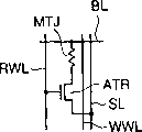
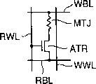
图88是示出具有磁隧道结部的存储单元(以下,也简单地称为「MTJ存储单元」)的结构的概略图。FIG. 88 is a schematic diagram showing the structure of a memory cell having a magnetic tunnel junction (hereinafter also simply referred to as "MTJ memory cell").
参照图88,MTJ存储单元具备其电阻值根据存储数据的数据电平而变化的磁隧道结部MTJ和存取晶体管ATR。存取晶体管ATR由场效应晶体管形成,被结合在磁隧道结部MTJ与接地电压Vss之间。Referring to FIG. 88, the MTJ memory cell includes a magnetic tunnel junction MTJ whose resistance value changes according to the data level of stored data, and an access transistor ATR. The access transistor ATR is formed of a field effect transistor, and is coupled between the magnetic tunnel junction MTJ and the ground voltage Vss.
对于MTJ存储单元来说,配置指示数据写入用的写入字线WWL、指示数据读出用的读出字线RWL和在数据读出时和数据写入时传递与存储数据的电平对应的电信号用的数据线、即位线BL。For the MTJ memory cell, configure the writing word line WWL for indicating data writing, the reading word line RWL for indicating data reading, and transfer the level corresponding to the stored data when reading and writing data. The data line for the electrical signal, that is, the bit line BL.
图89是说明来自MTJ存储单元的数据读出工作的概念图。Fig. 89 is a conceptual diagram illustrating an operation of reading data from an MTJ memory cell.
参照图89,磁隧道结部MTJ具有有恒定方向的固定磁场的磁性体层(以下,也简单地称为「固定磁层」)FL和有自由磁场的磁性体层(以下,也简单地称为「自由磁层」)VL。在固定磁层FL与自由磁层VL之间配置用绝缘体膜形成的隧道势垒TB。在自由磁层VL中,根据存储数据的电平,以非易失性的方式写入与固定磁层FL相同的方向的磁场和与固定磁层FL不同的方向的磁场的某一方。Referring to FIG. 89 , the magnetic tunnel junction MTJ has a magnetic layer (hereinafter, simply referred to as "fixed magnetic layer") FL having a fixed magnetic field in a constant direction and a magnetic layer (hereinafter, also simply referred to as "fixed magnetic layer") FL having a free magnetic field. is the "free magnetosphere") VL. Tunnel barrier TB formed of an insulator film is disposed between fixed magnetic layer FL and free magnetic layer VL. In free magnetic layer VL, either a magnetic field in the same direction as that of fixed magnetic layer FL or a magnetic field in a direction different from that of fixed magnetic layer FL is written in a nonvolatile manner depending on the level of stored data.
在数据读出时,存取晶体管ATR根据读出字线RWL的激活而被导通。由此,在位线BL~磁隧道结部MTJ~存取晶体管ATR~接地电压Vss的电流路径中,从未图示的控制电路流过作为恒定电流供给的读出电流Is。When reading data, access transistor ATR is turned on by activation of read word line RWL. Accordingly, the read current Is supplied as a constant current flows through a control circuit (not shown) in the current path from the bit line BL to the magnetic tunnel junction MTJ to the access transistor ATR to the ground voltage Vss.
磁隧道结部MTJ的电阻值根据固定磁层FL与自由磁层VL之间的磁场方向的相对关系而变化。具体地说,在固定磁层FL的磁场方向与写入到自由磁层VL中的磁场方向为相同的情况下,与两者的磁场方向不同的情况相比,磁隧道结部MTJ的电阻值变小。The resistance value of the magnetic tunnel junction MTJ varies according to the relative relationship of the magnetic field directions between the fixed magnetic layer FL and the free magnetic layer VL. Specifically, when the magnetic field direction of the fixed magnetic layer FL is the same as the magnetic field direction written in the free magnetic layer VL, the resistance value of the magnetic tunnel junction MTJ is lower than when the magnetic field directions of the two are different. get smaller.
因而,在数据读出时,由读出电流Is在磁隧道结部MTJ中产生的电压变化根据在自由磁层VL中存储的磁场方向而不同。由此如果在一度将位线BL预充电到规定的电压的状态后开始读出电流Is的供给,则利用位线BL的电压电平变化的监视,可读出MTJ存储单元的存储数据的电平。Therefore, at the time of data reading, the voltage change in the magnetic tunnel junction MTJ caused by the read current Is differs depending on the direction of the magnetic field stored in the free magnetic layer VL. Thus, if the supply of the sense current Is is started after the bit line BL is once precharged to a predetermined voltage, the voltage of the stored data in the MTJ memory cell can be read by monitoring the change in the voltage level of the bit line BL. flat.
图90是说明对于MTJ存储单元的数据写入工作的概念图。Fig. 90 is a conceptual diagram illustrating a data writing operation to an MTJ memory cell.
参照图90,在数据写入时,读出字线RWL被非激活,存取晶体管ATR被关断。在该状态下,对自由磁层VL写入磁场用的数据写入电流分别流过写入字线WWL和位线BL。自由磁层VL的磁场方向由分别流过写入字线WWL和位线BL的数据写入电流的方向的组合来决定。Referring to FIG. 90, during data writing, read word line RWL is deactivated, and access transistor ATR is turned off. In this state, a data write current for writing a magnetic field to free magnetic layer VL flows through write word line WWL and bit line BL, respectively. The direction of the magnetic field of the free magnetic layer VL is determined by a combination of directions of data write currents flowing through the write word line WWL and the bit line BL, respectively.
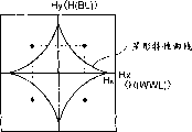
图91是说明数据写入时的数据写入电流的方向与磁场方向的关系的概念图。FIG. 91 is a conceptual diagram illustrating the relationship between the direction of the data writing current and the direction of the magnetic field during data writing.
参照图91,用横轴示出的磁场Hx表示由流过写入字线WWL的数据写入电流产生的磁场H(WWL)的方向。另一方面,在纵轴上示出的磁场Hy表示由流过位线BL的数据写入电流产生的磁场H(BL)的方向。Referring to FIG. 91 , the magnetic field Hx indicated by the horizontal axis indicates the direction of the magnetic field H(WWL) generated by the data write current flowing through the write word line WWL. On the other hand, the magnetic field Hy shown on the vertical axis indicates the direction of the magnetic field H(BL) generated by the data write current flowing through the bit line BL.
只在磁场H(WWL)与H(BL)的和到达图中示出的星形特性线的外侧的情况下,新写入在自由磁层VL中存储的磁场方向。即,在施加了与星形特性线的内侧的区域相当的磁场的情况下,不更新在自由磁层VL中存储的磁场方向。The magnetic field direction stored in the free magnetic layer VL is newly written only when the sum of the magnetic fields H(WWL) and H(BL) reaches the outside of the star-shaped characteristic line shown in the figure. That is, when a magnetic field corresponding to a region inside the star-shaped characteristic line is applied, the magnetic field direction stored in the free magnetic layer VL is not updated.
因而,为了利用写入工作来更新磁隧道结部MTJ的存储数据,必须使电流流过写入字线WWL和~这两者。在磁隧道结部MTJ中一度存储的磁场方向、即存储数据,在进行新的数据写入之前的期间内,以非易失性的方式被保持。Therefore, in order to update the stored data in the magnetic tunnel junction MTJ by the write operation, it is necessary to flow a current through both of the write word lines WWL and ˜. The magnetic field direction once stored in the magnetic tunnel junction MTJ, that is, stored data is held in a non-volatile manner until new data is written.
在数据读出时,在位线BL中也流过读出电流Is。但是,一般来说,由于将读出电流Is设定为比上述的数据写入电流小约1~2数量级,故因读出电流Is的影响而在数据读出时错误地改写MTJ存储单元的存储数据的可能性很小。During data reading, a read current Is also flows through the bit line BL. However, generally speaking, since the read current Is is set to be about 1 to 2 orders of magnitude smaller than the above-mentioned data write current, the MTJ memory cell is erroneously rewritten due to the influence of the read current Is during data read. There is little chance of storing data.
在上述的技术文献中,公开了在半导体衬底上集成这样的MTJ存储单元、构成作为随机存取存储器的MRAM器件的技术。The aforementioned technical documents disclose techniques for integrating such MTJ memory cells on a semiconductor substrate to constitute an MRAM device as a random access memory.
图92是示出以集成方式配置成行列状的MTJ存储单元的概念图。FIG. 92 is a conceptual diagram showing MTJ memory cells integrated in a matrix.
参照图92,通过在半导体衬底上将MTJ存储单元配置成行列状,可实现高集成化的MRAM器件。在图92中,示出将MTJ存储单元配置成n行×m列(n、m:自然数)的情况。Referring to FIG. 92, by arranging MTJ memory cells in rows and columns on a semiconductor substrate, a highly integrated MRAM device can be realized. FIG. 92 shows a case where MTJ memory cells are arranged in n rows×m columns (n, m: natural numbers).
如已说明的那样,对于各MTJ存储单元,必须配置位线BL、写入字线WWL和读出字线RWL。因而,对于配置成行列状的n×m个MTJ存储单元,必须配置n条写入字线WWL1~WWLn和读出字线RWL1~RWLn以及m条位线BL1~BLm。即,必须成为设置分别与读出工作和写入工作对应的、独立的字线的结构。As already described, bit line BL, write word line WWL, and read word line RWL must be arranged for each MTJ memory cell. Therefore, for n×m MTJ memory cells arranged in rows and columns, n write word lines WWL1 to WWLn, read word lines RWL1 to RWLn and m bit lines BL1 to BLm must be arranged. That is, it is necessary to have a structure in which independent word lines corresponding to the read operation and the write operation are respectively provided.
图93是在半导体衬底上配置的MTJ存储单元的结构图。Fig. 93 is a structural diagram of an MTJ memory cell arranged on a semiconductor substrate.
参照图93,在半导体主衬底SUB上的p型区PAR中形成存取晶体管ATR。存取晶体管ATR具有作为n型区的源/漏区110、120和栅130。源/漏区110经在第1金属布线层M1中形成的金属布线与接地电压Vss结合。使用在第2金属布线层M2中形成的金属布线作为写入字线WWL。此外,在第3金属布线层M3中设置位线BL。Referring to FIG. 93, an access transistor ATR is formed in a p-type region PAR on the semiconductor main substrate SUB. The access transistor ATR has source/
磁隧道结部MTJ配置在设置写入字线WWL的第2金属布线层M2与设置位线BL的第3金属布线层M3之间。存取晶体管ATR的源/漏区120经在接触孔中形成的金属膜150、第1和第2金属布线层M1和M2以及阻挡金属140与磁隧道结部MTJ导电性地结合。阻挡金属140是为了导电性地结合磁隧道结部MTJ与金属布线之间而设置的缓冲材料。The magnetic tunnel junction MTJ is arranged between the second metal wiring layer M2 on which the write word line WWL is provided and the third metal wiring layer M3 on which the bit line BL is provided. The source/
如已说明的那样,在各MTJ存储单元中,作为独立的布线,设置读出字线RWL和写入字线WWL。此外,必须在数据写入时在写入字线WWL和位线BL中流过发生规定值以上的大小的磁场用的数据写入电流。因而,使用金属布线来形成位线BL和写入字线WWL。As already described, in each MTJ memory cell, a read word line RWL and a write word line WWL are provided as independent wirings. In addition, a data write current for generating a magnetic field having a magnitude equal to or greater than a predetermined value must flow through write word line WWL and bit line BL at the time of data write. Thus, the bit line BL and the write word line WWL are formed using metal wiring.
另一方面,读出字线RWL是为了控制存取晶体管ATR的栅电压而设置的,没有必要以积极的方式流过电流。因而,从提高集成度的观点来看,不是新设置独立的金属布线层、而是在与栅130为同一的布线层中使用多晶硅层或多晶硅硅化物(policide)结构来形成读出字线RWL。On the other hand, the read word line RWL is provided to control the gate voltage of the access transistor ATR, and it is not necessary to flow a positive current. Therefore, from the viewpoint of improving integration, instead of newly providing an independent metal wiring layer, a polysilicon layer or a polysilicon silicide (poliicide) structure is used in the same wiring layer as the
这样,因为在数据读出和数据写入中必要的布线很多,故在半导体衬底上以集成的方式配置MTJ存储单元的情况下,存在因这些布线的配置空间的关系而使单元尺寸变得大型化的问题。In this way, since there are many wirings necessary for data reading and data writing, when MTJ memory cells are arranged in an integrated manner on a semiconductor substrate, there is a possibility that the cell size becomes smaller due to the arrangement space of these wirings. problem of overscaling.
此外,为了谋求MTJ存储单元的集成化,必须减小布线的间距或增加布线层的数目,导致了因处理工序的复杂化引起的制造成本的上升。Furthermore, in order to integrate MTJ memory cells, it is necessary to reduce the wiring pitch or increase the number of wiring layers, resulting in an increase in manufacturing cost due to the complexity of the processing steps.
再者,因为布线数和布线层数很多,不得不采用分别在字线与位线的交点处配置MTJ存储单元的所谓的交叉点配置,故难以充分地确保在数据读出和数据写入的工作容限。Furthermore, since the number of wiring lines and the number of wiring layers are large, a so-called cross-point configuration in which MTJ memory cells are respectively arranged at the intersections of word lines and bit lines has to be adopted, so it is difficult to sufficiently ensure the gap between data read and data write. working tolerance.
此外,在数据写入时,必须在位线BL中流过较大的数据写入电流,而且,根据写入数据的电平,必须控制该数据写入电流的方向。因此,也存在控制数据写入电流用的电路变得复杂的问题。Also, at the time of data writing, a large data writing current must flow through the bit line BL, and the direction of the data writing current must be controlled according to the level of the data to be written. Therefore, there is also a problem that the circuit for controlling the data writing current becomes complicated.
发明内容Contents of the invention
本发明的目的在于,在具有MTJ存储单元的MRAM器件中,削减在存储器阵列的整体中配置的布线数,谋求MRAM器件的高集成化。An object of the present invention is to reduce the number of wires arranged in the entire memory array in an MRAM device having an MTJ memory cell, and achieve high integration of the MRAM device.
如果将本发明归纳起来,则它是一种薄膜磁性体存储器,具备存储器阵列、多条读出字线、多条数据线、多条写入字线和多条基准电压布线。存储器阵列的具有配置成行列状的多个磁性体存储单元的每一个包括:磁存储部,其电阻值根据由第1和第2数据写入电流写入的存储数据的电平而变化;以及存储单元选择门,用来在数据读出时使数据读出电流(Is)通过上述磁存储部。多条读出字线与上述磁性体存储单元的行对应地设置,用来在上述数据读出时根据行选择结果使对应的上述存储单元选择门工作。多条数据线与上述磁性体存储单元的列对应地设置,用来在数据写入时和上述数据读出时分别流过上述第1数据写入电流和上述数据读出电流。多条写入字线上述行对应地设置,为了在上述数据写入时流过上述第2数据写入电流,根据行选择结果有选择地被激活。多条基准电压布线与行和上述列的某一个对应地设置,供给在上述数据读出时使用的基准电压。邻接的上述磁性体存储单元共有上述多条写入字线、上述多条读出字线、上述多条数据线和上述多条基准电压布线中的至少1个中的对应的1条。If the present invention is summed up, it is a thin film magnetic memory, which has a memory array, a plurality of read word lines, a plurality of data lines, a plurality of write word lines and a plurality of reference voltage wirings. Each of the plurality of magnetic memory cells arranged in rows and columns of the memory array includes: a magnetic storage portion whose resistance value changes according to the level of stored data written by the first and second data writing currents; and The memory cell selection gate is used to pass the data read current (Is) through the above-mentioned magnetic storage part when reading data. A plurality of read word lines are arranged corresponding to the rows of the magnetic memory cells, and are used to make the corresponding memory cell selection gates work according to the row selection results when the data is read. A plurality of data lines are provided corresponding to the columns of the magnetic memory cells, for passing the first data writing current and the data reading current during data writing and data reading, respectively. A plurality of write word lines are provided corresponding to the rows, and are selectively activated according to a row selection result in order to flow the second data write current during the data write. A plurality of reference voltage wirings are provided corresponding to any one of the row and the column, and supply the reference voltage used for reading the data. Adjacent magnetic memory cells share at least one corresponding one of the plurality of write word lines, the plurality of read word lines, the plurality of data lines, and the plurality of reference voltage wirings.
因而,本发明的主要的优点是,在具备使用写入字线、读出字线、数据线和基准电压布线进行数据读出和数据写入的磁性体存储单元的薄膜磁性体存储器中,可削减在存储器阵列中设置的布线数。其结果,可使存储器阵列实现高集成化、削减芯片面积。Therefore, the main advantage of the present invention is that in a thin-film magnetic storage device that uses a write-in word line, a read-out word line, a data line, and a reference voltage wiring to perform data readout and data write-in magnetic memory cells, The number of wires provided in the memory array is reduced. As a result, the memory array can be highly integrated and the chip area can be reduced.
按照本发明的另一方面,是一种薄膜磁性体存储器,具备存储器阵列、多条读出字线、多条数据线、多条写入字线和字线电流控制电路。存储器阵列具有配置成行列状的多个磁性体存储单元。上述多个磁性体存储单元的每一个包括:磁存储部,其电阻值根据由第1和第2数据写入电流写入的存储数据的电平而变化;以及存储单元选择门,用来在数据读出时使数据读出电流通过上述磁存储部。多条读出字线与上述磁性体存储单元的行对应地设置,在上述数据读出时根据行选择结果使对应的上述存储单元选择门工作。多条数据线与上述磁性体存储单元的列对应地设置,在数据写入时和上述数据读出时分别流过上述第1数据写入电流和上述数据读出电流。多条写入字线与上述行对应地设置,为了在上述数据写入时流过上述第2数据写入电流,根据行选择结果有选择地被激活。字线电流控制电路结合在数据读出中使用的基准电压(Vss)与上述多条写入字线。邻接的上述磁性体存储单元共有上述多条写入字线、上述多条读出字线和上述多条数据线中的至少1个中的对应的1条。According to another aspect of the present invention, it is a thin film magnetic memory, which has a memory array, a plurality of read word lines, a plurality of data lines, a plurality of write word lines and a word line current control circuit. A memory array has a plurality of magnetic memory cells arranged in rows and columns. Each of the plurality of magnetic memory cells includes: a magnetic memory portion whose resistance value varies according to the level of stored data written by the first and second data write currents; and a memory cell selection gate for When data is read, a data read current is passed through the magnetic storage unit. A plurality of read word lines are provided corresponding to the rows of the magnetic memory cells, and the corresponding memory cell selection gates are operated according to the row selection results when the data is read. A plurality of data lines are provided corresponding to the columns of the magnetic memory cells, and the first data writing current and the data reading current flow respectively during data writing and data reading. A plurality of write word lines are provided corresponding to the row, and are selectively activated in accordance with a row selection result in order to flow the second data write current during the data write. The word line current control circuit combines a reference voltage (Vss) used in data readout with the above-mentioned plurality of write word lines. The adjacent magnetic memory cells share at least one corresponding one of the plurality of write word lines, the plurality of read word lines, and the plurality of data lines.
因而,可削减在配置使用写入字线、读出字线和数据线进行数据读出和数据写入的磁性体存储单元的存储器阵列中设置的布线数。其结果,可使存储器阵列实现高集成化、削减芯片面积。Therefore, it is possible to reduce the number of wires provided in a memory array in which magnetic memory cells for data reading and data writing are arranged using write word lines, read word lines, and data lines. As a result, the memory array can be highly integrated and the chip area can be reduced.
按照本发明的又一方面,是一种薄膜磁性体存储器,具备存储器阵列、多条读出字线、多条信号布线、读出写入控制电路、多条写入字线和多个控制开关。存储器阵列具有配置成行列状的多个磁性体存储单元。上述多个磁性体存储单元的每一个包括:磁存储部,其电阻值根据由第1和第2数据写入电流写入的存储数据的电平而变化;以及存储单元选择门,用来在数据读出时使数据读出电流(Is)通过上述磁存储部。多条读出字线与上述磁性体存储单元的行对应地设置,在上述数据读出时根据行选择结果使对应的上述存储单元选择门工作。多条信号布线与上述磁性体存储单元的列对应地设置。在行方向上邻接的上述磁性体存储单元共有上述多条信号布线中的对应的1条。读出写入控制电路在数据写入时和上述数据读出时将上述第1数据写入电流和上述数据读出电流供给上述信号布线。多条写入字线与上述行对应地设置,为了在上述数据写入时流过上述第2数据写入电流,根据行选择结果有选择地被激活。多个控制开关分别与上述多条信号布线对应地设置,导电性地结合在上述数据读出中使用的基准电压与上述多条信号布线中的对应的1条。上述多个控制开关将与各上述磁性体存储单元对应的2条上述信号布线中的根据上述列选择结果被选择的1条与上述基准电压结合。According to still another aspect of the present invention, it is a thin film magnetic memory, comprising a memory array, a plurality of read word lines, a plurality of signal wiring lines, a read write control circuit, a plurality of write word lines, and a plurality of control switches . A memory array has a plurality of magnetic memory cells arranged in rows and columns. Each of the plurality of magnetic memory cells includes: a magnetic memory portion whose resistance value varies according to the level of stored data written by the first and second data write currents; and a memory cell selection gate for When data is read, a data read current (Is) is passed through the magnetic storage unit. A plurality of read word lines are provided corresponding to the rows of the magnetic memory cells, and the corresponding memory cell selection gates are operated according to the row selection results when the data is read. A plurality of signal wires are provided corresponding to the columns of the above-mentioned magnetic memory cells. The magnetic memory cells adjacent in the row direction share a corresponding one of the plurality of signal wirings. The read/write control circuit supplies the first data write current and the data read current to the signal wiring during data writing and data reading. A plurality of write word lines are provided corresponding to the row, and are selectively activated in accordance with a row selection result in order to flow the second data write current during the data write. A plurality of control switches are provided corresponding to the plurality of signal wirings, and conductively connect the reference voltage used for the data readout to a corresponding one of the plurality of signal wirings. The plurality of control switches connect one of the two signal wires corresponding to each of the magnetic memory cells selected based on the column selection result to the reference voltage.
在这样的薄膜磁性体存储器中,可削减共有布线的布线数、在存储器阵列中配置使用同时具有写入字线、读出字线、数据线和基准电压布线的功能的共有布线进行数据读出和数据写入的磁性体存储单元。其结果,可使存储器阵列实现高集成化、削减芯片面积。In such a thin film magnetic memory, the number of common wirings can be reduced, and data can be read by arranging and using shared wirings that simultaneously function as write word lines, read word lines, data lines, and reference voltage wirings in the memory array. And the magnetic storage unit for data writing. As a result, the memory array can be highly integrated and the chip area can be reduced.
按照本发明的又一方面,是一种薄膜磁性体存储器,具备存储器阵列、多条写入字线、多条读出字线、多条写入数据线和多条读出数据线。存储器阵列具有配置成行列状的多个磁性体存储单元。多个磁性体存储单元的每一个包括:磁存储部,其电阻值根据在由第1和第2数据写入电流施加的数据写入磁场比规定磁场大的情况下写入的存储数据的电平而变化;以及存储单元选择门,用来在数据读出时使数据读出电流(Is)通过上述磁存储部。多条写入字线与上述行对应地设置,为了在数据写入时流过上述第2数据写入电流,根据行选择结果有选择地被激活。多条读出字线与上述磁性体存储单元的行对应地设置,在数据读出时根据行选择结果使对应的上述存储单元选择门工作。多条写入数据线与上述磁性体存储单元的列对应地设置,用来在上述数据写入时流过上述第2数据写入电流。多条读出数据线与上述磁性体存储单元的列对应地设置,在数据读出时流过数据读出电流。邻接的磁性体存储单元共有多条写入字线、多条读出字线、多条读出数据线和多条写入数据线中的至少1个中的对应的1条。According to still another aspect of the present invention, it is a thin film magnetic memory, which includes a memory array, a plurality of write word lines, a plurality of read word lines, a plurality of write data lines, and a plurality of read data lines. A memory array has a plurality of magnetic memory cells arranged in rows and columns. Each of the plurality of magnetic memory cells includes a magnetic storage portion whose resistance value is based on the electrical resistance of the stored data written when the data writing magnetic field applied by the first and second data writing currents is larger than a predetermined magnetic field. and a memory cell selection gate for passing a data read current (Is) through the above-mentioned magnetic storage portion when reading data. A plurality of write word lines are provided corresponding to the row, and are selectively activated in accordance with a row selection result so that the second data write current flows during data writing. A plurality of read word lines are arranged corresponding to the rows of the magnetic memory cells, and the corresponding memory cell selection gates are activated according to the row selection results during data reading. A plurality of write data lines are provided corresponding to the columns of the magnetic memory cells for passing the second data write current during the data write. A plurality of read data lines are provided corresponding to the columns of the magnetic memory cells, and a data read current flows during data read. Adjacent magnetic memory cells share at least one corresponding one of the plurality of write word lines, the plurality of read word lines, the plurality of read data lines, and the plurality of write data lines.
在这样的薄膜磁性体存储器中,可削减在配置使用写入字线、读出字线、写入数据线和读出数据线进行数据读出和数据写入的磁性体存储单元的存储器阵列中设置的布线数。其结果,可使存储器阵列实现高集成化、削减芯片面积。In such a thin-film magnetic memory, it is possible to reduce the number of memory arrays in which magnetic memory cells that use write word lines, read word lines, write data lines, and read data lines for data read and data write are arranged. The number of wires to set. As a result, the memory array can be highly integrated and the chip area can be reduced.
通过参照附图的后述的本发明的详细的说明,本发明的上述和其它的目的、特征、方面和优点会变得更加明白。The above and other objects, features, aspects, and advantages of the present invention will become more apparent from the detailed description of the present invention to be described later with reference to the accompanying drawings.
附图说明Description of drawings
图1是示出本发明的实施例1的MRAM器件1的整体结构的概略框图。FIG. 1 is a schematic block diagram showing the overall configuration of an
图2是示出实施例1的MTJ存储单元与信号布线之间的连接关系的电路图。FIG. 2 is a circuit diagram showing a connection relationship between an MTJ memory cell and signal wiring in
图3是说明对于实施例1的存储单元的数据写入和数据读出的时序图。3 is a timing chart illustrating data writing and data reading to the memory cell of the first embodiment.
图4是说明实施例1的存储单元的配置的结构图。FIG. 4 is a structural diagram illustrating the configuration of a memory cell of
图5是示出实施例1的存储器阵列10的结构的框图。FIG. 5 is a block diagram showing the structure of the
图6是示出实施例1的变形例1的存储器阵列10的结构的框图。FIG. 6 is a block diagram showing the configuration of a
图7是示出实施例1的变形例2的存储器阵列10的结构的框图。FIG. 7 is a block diagram showing the configuration of a
图8A和图8B是说明写入字线WWL的配置的结构图。8A and 8B are structural diagrams illustrating the configuration of write word lines WWL.
图9是示出实施例1的变形例3的存储器阵列10的结构的框图。FIG. 9 is a block diagram showing the configuration of a
图10是示出实施例1的变形例4的存储器阵列10的结构的框图。FIG. 10 is a block diagram showing the configuration of a
图11是示出实施例1的变形例5的存储器阵列10和外围电路的结构的框图。FIG. 11 is a block diagram showing configurations of a
图12是示出与共同布线控制晶体管CCT的导通/关断对应的共同布线SBL的工作的时序图。FIG. 12 is a timing chart showing the operation of the common wiring SBL corresponding to on/off of the common wiring control transistor CCT.
图13是示出实施例2的存储器阵列10和外围电路的结构的框图。FIG. 13 is a block diagram showing the configuration of the
图14是示出数据写入电路50w和数据读出电路50r的结构的电路图。FIG. 14 is a circuit diagram showing configurations of a
图15是示出实施例2的变形例1的存储器阵列10和外围电路的结构的框图。FIG. 15 is a block diagram showing configurations of a
图16是示出实施例2的变形例2的存储器阵列10和外围电路的结构的框图。FIG. 16 is a block diagram showing the configuration of a
图17是示出数据读出电路50r的结构的电路图。FIG. 17 is a circuit diagram showing the configuration of the
图18是示出实施例3的存储单元与信号布线之间的连接关系的电路图。FIG. 18 is a circuit diagram showing a connection relationship between memory cells and signal wirings in Embodiment 3. FIG.
图19是说明实施例3的存储单元的配置的结构图。FIG. 19 is a structural diagram illustrating the configuration of a memory cell of Embodiment 3. FIG.
图20是示出实施例3的存储器阵列10的结构的框图。FIG. 20 is a block diagram showing the structure of the
图21是示出实施例3的变形例1的存储器阵列10的结构的框图。FIG. 21 is a block diagram showing the configuration of a
图22是示出实施例3的变形例2的存储器阵列10的结构的框图。FIG. 22 is a block diagram showing the configuration of a
图23是示出实施例3的变形例3的存储器阵列10的结构的框图。FIG. 23 is a block diagram showing the configuration of a
图24是示出实施例3的变形例4的存储器阵列10的结构的框图。FIG. 24 is a block diagram showing the configuration of a
图25是示出实施例3的变形例5的存储器阵列10和外围电路的结构的框图。FIG. 25 is a block diagram showing configurations of a
图26是示出实施例3的变形例6的存储器阵列10和外围电路的结构的框图。FIG. 26 is a block diagram showing configurations of a
图27是示出实施例3的变形例7的存储器阵列10和外围电路的结构的框图。FIG. 27 is a block diagram showing the configuration of a
图28是示出实施例3的变形例8的存储器阵列10和外围电路的结构的框图。FIG. 28 is a block diagram showing the configuration of a
图29是示出实施例4的存储单元与信号布线之间的连接关系的电路图。FIG. 29 is a circuit diagram showing a connection relationship between memory cells and signal wirings in
图30是说明实施例4的存储单元的配置的结构图。Fig. 30 is a structural diagram illustrating the configuration of a memory cell of the fourth embodiment.
图31是示出实施例4的存储器阵列10的结构的框图。FIG. 31 is a block diagram showing the structure of the
图32是示出实施例4的变形例1的存储器阵列10的结构的框图。FIG. 32 is a block diagram showing the configuration of a
图33是示出实施例4的变形例2的存储器阵列10的结构的框图。FIG. 33 is a block diagram showing the configuration of a
图34是示出实施例4的变形例3的存储器阵列10的结构的框图。FIG. 34 is a block diagram showing the configuration of a
图35是示出实施例4的变形例4的存储器阵列10的结构的框图。FIG. 35 is a block diagram showing the configuration of a
图36是示出实施例4的变形例5的存储器阵列10的结构的框图。FIG. 36 is a block diagram showing the configuration of a
图37是示出实施例4的变形例6的存储器阵列10和外围电路的结构的框图。FIG. 37 is a block diagram showing configurations of a
图38是示出实施例4的变形例7的存储器阵列10和外围电路的结构的框图。FIG. 38 is a block diagram showing the configuration of a
图39是示出实施例4的变形例8的存储器阵列10和外围电路的结构的框图。FIG. 39 is a block diagram showing the configuration of a
图40是示出实施例5的存储单元与信号布线之间的连接关系的电路图。FIG. 40 is a circuit diagram showing a connection relationship between memory cells and signal wirings in
图41是说明实施例5的存储单元的配置的结构图。Fig. 41 is a structural diagram illustrating the configuration of a memory cell of the fifth embodiment.
图42是示出实施例5的存储器阵列10的结构的框图。FIG. 42 is a block diagram showing the structure of the
图43是示出实施例5的变形例1的存储器阵列10的结构的框图。FIG. 43 is a block diagram showing the configuration of a
图44是示出实施例5的变形例2的存储器阵列10的结构的框图。FIG. 44 is a block diagram showing the configuration of a
图45是示出实施例5的变形例3的存储器阵列10的结构的框图。FIG. 45 is a block diagram showing the configuration of a
图46是示出实施例5的变形例4的存储器阵列10的结构的框图。FIG. 46 is a block diagram showing the configuration of a
图47是示出实施例5的变形例5的存储器阵列10的结构的框图。FIG. 47 is a block diagram showing the configuration of a
图48是示出实施例5的变形例6的存储器阵列10和外围电路的结构的框图。FIG. 48 is a block diagram showing the configuration of a
图49是示出实施例5的变形例7的存储器阵列10和外围电路的结构的框图。FIG. 49 is a block diagram showing the configuration of a
图50是示出实施例5的变形例8的存储器阵列10和外围电路的结构的框图。FIG. 50 is a block diagram showing the configuration of a
图51是示出实施例6的MTJ存储单元与信号布线之间的连接关系的电路图。FIG. 51 is a circuit diagram showing the connection relationship between the MTJ memory cell and the signal wiring of the sixth embodiment.
图52是说明实施例6的MTJ存储单元的配置的结构图。Fig. 52 is a structural diagram illustrating the arrangement of an MTJ memory cell of the sixth embodiment.
图53是示出实施例6的存储器阵列10的结构的框图。FIG. 53 is a block diagram showing the structure of the
图54是示出实施例6的变形例1的存储器阵列10的结构的框图。FIG. 54 is a block diagram showing the configuration of a
图55是示出实施例6的变形例2的存储器阵列10的结构的框图。FIG. 55 is a block diagram showing the configuration of a
图56是示出实施例6的变形例3的存储器阵列10的结构的框图。FIG. 56 is a block diagram showing the configuration of a
图57是示出实施例6的变形例4的存储器阵列10和外围电路的结构的框图。FIG. 57 is a block diagram showing the configuration of a
图58是示出实施例6的变形例5的存储器阵列10和外围电路的结构的框图。FIG. 58 is a block diagram showing the configuration of a
图59是示出实施例6的变形例6的存储器阵列10和外围电路的结构的框图。FIG. 59 is a block diagram showing configurations of a
图60是示出实施例7的存储单元与信号布线之间的连接关系的电路图。FIG. 60 is a circuit diagram showing the connection relationship between memory cells and signal wirings in
图61是说明实施例7的存储单元的配置的结构图。Fig. 61 is a structural diagram illustrating the arrangement of memory cells of the seventh embodiment.
图62是示出实施例7的存储器阵列10的结构的框图。FIG. 62 is a block diagram showing the structure of the
图63是示出实施例7的变形例1的存储器阵列10的结构的框图。FIG. 63 is a block diagram showing the configuration of a
图64是示出实施例7的变形例2的存储器阵列10的结构的框图。FIG. 64 is a block diagram showing the configuration of a
图65是示出实施例7的变形例3的存储器阵列10的结构的框图。FIG. 65 is a block diagram showing the configuration of a
图66是示出实施例7的变形例4的存储器阵列10和外围电路的结构的框图。FIG. 66 is a block diagram showing the configuration of a
图67是示出实施例7的变形例5的存储器阵列10和外围电路的结构的框图。FIG. 67 is a block diagram showing the configuration of a
图68是示出实施例7的变形例6的存储器阵列10和外围电路的结构的框图。FIG. 68 is a block diagram showing the configuration of a
图69是示出实施例8的存储单元与信号布线之间的连接关系的电路图。FIG. 69 is a circuit diagram showing the connection relationship between memory cells and signal wirings in the eighth embodiment.
图70是说明对于实施例8的MTJ存储单元的数据写入和数据读出的时序图。Fig. 70 is a timing chart explaining data writing and data reading with respect to the MTJ memory cell of the eighth embodiment.
图71是说明实施例8的MTJ存储单元的配置的结构图。Fig. 71 is a structural diagram illustrating the arrangement of an MTJ memory cell of the eighth embodiment.
图72是示出实施例8的存储器阵列10的结构的框图。FIG. 72 is a block diagram showing the structure of the
图73是示出实施例8的变形例1的存储器阵列10的结构的框图。FIG. 73 is a block diagram showing the configuration of a
图74是示出实施例8的变形例2的存储器阵列10的结构的框图。FIG. 74 is a block diagram showing the configuration of a
图75是示出实施例8的变形例3的存储器阵列10的结构的框图。FIG. 75 is a block diagram showing the configuration of a
图76是示出实施例8的变形例4的存储器阵列10和外围电路的结构的框图。FIG. 76 is a block diagram showing the configuration of a
图77是示出实施例8的变形例5的存储器阵列10和外围电路的结构的框图。FIG. 77 is a block diagram showing the configuration of a
图78是示出实施例8的变形例6的存储器阵列10和外围电路的结构的框图。FIG. 78 is a block diagram showing the configuration of a
图79是示出实施例9的存储单元与信号布线之间的连接关系的电路图。FIG. 79 is a circuit diagram showing the connection relationship between memory cells and signal wirings in Embodiment 9. FIG.
图80是说明实施例9的MTJ存储单元的配置的结构图。Fig. 80 is a structural diagram illustrating the arrangement of an MTJ memory cell of the ninth embodiment.
图81是示出实施例9的存储器阵列10的结构的框图。FIG. 81 is a block diagram showing the structure of the
图82是示出实施例9的变形例1的存储器阵列10的结构的框图。FIG. 82 is a block diagram showing the configuration of a
图83是示出实施例9的变形例2的存储器阵列10的结构的框图。FIG. 83 is a block diagram showing the configuration of a
图84是示出实施例9的变形例3的存储器阵列10的结构的框图。FIG. 84 is a block diagram showing the configuration of a
图85是示出实施例9的变形例4的存储器阵列10和外围电路的结构的框图。FIG. 85 is a block diagram showing the configuration of a
图86是示出实施例9的变形例5的存储器阵列10和外围电路的结构的框图。FIG. 86 is a block diagram showing the configuration of a
图87是示出实施例9的变形例6的存储器阵列10和外围电路的结构的框图。FIG. 87 is a block diagram showing the configuration of a
图88是示出具有磁隧道结部的存储单元的结构的概略图。FIG. 88 is a schematic diagram showing the structure of a memory cell having a magnetic tunnel junction.
图89是说明来自MTJ存储单元的数据读出工作的概念图。Fig. 89 is a conceptual diagram illustrating an operation of reading data from an MTJ memory cell.
图90是说明对于MTJ存储单元的数据写入工作的概念图。Fig. 90 is a conceptual diagram illustrating a data writing operation to an MTJ memory cell.
图91是说明数据写入时的数据写入电流的方向与磁场方向的关系的概念图。FIG. 91 is a conceptual diagram illustrating the relationship between the direction of the data writing current and the direction of the magnetic field during data writing.
图92是示出以集成的方式配置成行列状的MTJ存储单元的概念图。FIG. 92 is a conceptual diagram showing MTJ memory cells integrated in a matrix.
图93是在半导体衬底上配置的MTJ存储单元的结构图。Fig. 93 is a structural diagram of an MTJ memory cell arranged on a semiconductor substrate.
具体实施方式Detailed ways
以下,参照附图详细地说明本发明的实施例。Hereinafter, embodiments of the present invention will be described in detail with reference to the drawings.
实施例1Example 1
参照图1,本发明的实施例1的MRAM器件1响应于来自外部的控制信号CMD和地址信号ADD进行随机存取,进行写入数据DIN的输入和读出数据DOUT的输出。Referring to FIG. 1 , the
MRAM器件1具备:响应于控制信号CMD来控制MRAM器件1的整体工作的控制电路5;以及具有配置成行列状的多个MTJ存储单元(以下,也简单地称为「存储单元」)的存储器阵列10。存储器阵列10的结构在后面详细地说明,但与MTJ存储单元的行(以下,也简单地称为「存储单元行」)对应地配置多条写入字线WWL和读出字线RWL,与MTJ存储单元的列(以下,也简单地称为「存储单元列」)对应地配置多条位线BL和基准电压布线SL。The
MRAM器件1还具备:行译码器20,根据由地址信号ADD示出的行地址RA的译码结果,进行存储器阵列10中的行选择;列译码器25,根据由地址信号ADD示出的列地址CA的译码结果,进行存储器阵列10中的列选择;字线驱动器30,用来根据行译码器20的行选择结果有选择地激活读出字线RWL和写入字线WWL;字线电流控制电路40,用来在数据写入时在写入字线WWL中流过数据写入电流;读出/写入控制电路50、60,用来在数据读出和数据写入时分别流过数据写入电流和读出电流。The
读出/写入控制电路50、60控制存储器阵列10的两端部的位线BL的电压电平,在位线BL中流过用来分别进行数据写入和数据读出的数据写入电流和读出电流。The read/
存储单元的结构和工作The structure and operation of the storage unit
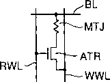
参照图2,对于实施例1的MTJ存储单元,设置读出字线RWL、写入字线WWL、位线BL和基准电压布线SL。Referring to FIG. 2, for the MTJ memory cell of
存储单元包含串联地结合的磁隧道结部MTJ和存取晶体管ATR。如已说明的那样,代表性地应用在半导体衬底上形成的场效应晶体管、即MOS晶体管作为存取晶体管ATR。The memory cell includes a magnetic tunnel junction MTJ and an access transistor ATR coupled in series. As already described, a field effect transistor formed on a semiconductor substrate, that is, a MOS transistor is typically used as the access transistor ATR.
存取晶体管ATR的栅与读出字线RWL结合。如果读出字线RWL被激活为选择状态(高电平,电源电压Vcc),则存取晶体管ATR导通,导电性地结合磁隧道结部MTJ与基准电压布线SL。基准电压布线SL供给接地电压Vss。将磁隧道结部MTJ导电性地结合在位线BL与存取晶体管ATR之间。The gate of access transistor ATR is coupled to read word line RWL. When read word line RWL is activated in a selected state (high level, power supply voltage Vcc), access transistor ATR is turned on, and magnetic tunnel junction MTJ and reference voltage line SL are electrically connected. The ground voltage Vss is supplied to the reference voltage line SL. Magnetic tunnel junction MTJ is conductively coupled between bit line BL and access transistor ATR.
因而,响应于存取晶体管ATR的导通,形成位线BL~磁隧道结部MTJ~存取晶体管ATR~基准电压布线SL的电流路径。通过使读出电流Is流过该电流路径,在位线BL上产生与磁隧道结部MTJ的存储数据的电平对应的电压变化。Therefore, in response to the conduction of the access transistor ATR, a current path from the bit line BL to the magnetic tunnel junction MTJ to the access transistor ATR to the reference voltage wiring SL is formed. By passing the read current Is through this current path, a voltage change corresponding to the level of the stored data in the magnetic tunnel junction MTJ occurs on the bit line BL.
另一方面,在读出字线RWL被非激活为非选择状态(低电平,接地电压Vss)的情况下,存取晶体管ATR被关断,导电性地隔断位线BL与存取晶体管ATR之间。On the other hand, when the read word line RWL is deactivated to a non-selected state (low level, ground voltage Vss), the access transistor ATR is turned off, and the bit line BL and the access transistor ATR are electrically isolated. between.
与读出字线RWL平行地、接近于磁隧道结部MTJ设置写入字线WWL。在数据写入时,在写入字线WWL和位线BL中流过数据写入电流。利用由这些数据写入电流分别产生的磁场的和改写存储单元的存储数据的电平。Write word line WWL is provided in parallel to read word line RWL and close to magnetic tunnel junction MTJ. At the time of data writing, a data writing current flows through writing word line WWL and bit line BL. The levels of the stored data of the memory cells are rewritten by the sum of the magnetic fields respectively generated by these data writing currents.
其次,使用图3,说明对于实施例1的存储单元的数据写入和数据读出。Next, data writing and data reading with respect to the memory cell of Example 1 are demonstrated using FIG. 3. FIG.
首先,说明数据写入时的工作。First, the operation at the time of data writing will be described.
字线驱动器30根据行译码器20的行选择结果,将与选择行对应的写入字线WWL的电压驱动为选择状态(高电平)。在非选择行中,将写入字线WWL的电压电平维持为非选择状态(低电平)。The
读出字线RWL在数据写入时不被激活,维持为非选择状态(低电平)。由于利用字线电流控制电路40将各写入字线WWL与接地电压Vss结合,故在选择行的写入字线WWL中流过数据写入电流Ip。另一方面,在非选择行的写入字线WWL中不流过数据写入电流。Read word line RWL is not activated during data writing, and remains in a non-selected state (low level). Since each write word line WWL is connected to the ground voltage Vss by the word line
读出/写入控制电路50和60通过控制存储器阵列10两端的位线BL的电压,产生与写入数据的数据电平对应的方向的数据写入电流。例如,在写入“1”的存储数据的情况下,将读出/写入控制电路60侧的位线电压设定为高电压状态(电源电压Vcc),将相反一侧的读出/写入控制电路50侧的位线电压设定为低电压状态(接地电压Vss)。由此,在从读出/写入控制电路60朝向50的方向上,数据写入电流+Iw流过位线BL。另一方面,在写入“0”的存储数据的情况下,将读出/写入控制电路50侧和60侧的位线电压分别设定为高电压状态(电源电压Vcc)和低电压状态(接地电压Vss),在从读出/写入控制电路50朝向60的方向上,数据写入电流-Iw流过位线BL。The read/
此时,没有必要使数据写入电流±Iw流过各位线BL,读出/写入控制电路50和60根据列译码器25的列选择结果,可这样来控制上述的位线BL的电压,使数据写入电流±Iw有选择地流过与选择列对应的至少1条位线。At this time, it is not necessary to flow the data write current ±Iw through the bit lines BL, and the read/
这样,通过设定数据写入电流Ip和±Iw的方向,在数据写入时,根据被写入的存储数据的电平“1”、“0”,选择反方向的数据写入电流+Iw和-Iw的某一方,将写入字线WWL的数据写入电流Ip与数据电平无关地固定为恒定方向,由此,可始终使流过写入字线WWL的数据写入电流Ip的方向为恒定。其结果,如以下所说明的那样,可简化字线电流控制电路40的结构。In this way, by setting the direction of the data writing current Ip and ±Iw, during data writing, according to the level "1" and "0" of the stored data to be written, the data writing current +Iw in the opposite direction is selected. One of -Iw and -Iw fixes the data writing current Ip in the writing word line WWL to a constant direction regardless of the data level, thereby making it possible to always make the data writing current Ip flowing in the writing word line WWL direction is constant. As a result, the configuration of the word line
其次,说明数据读出时的工作。Next, the operation at the time of data reading will be described.
在数据读出时,字线驱动器30根据行译码器20的行选择结果,将与选择行对应的读出字线RWL的电压驱动为选择状态(高电平)。在非选择行中,将读出字线RWL的电压电平维持为非选择状态(低电平)。在数据写入时写入字线WWL不被激活,维持为非选择状态(低电平)。When reading data,
在数据读出之前,例如将位线BL预充电为高电压状态(电源电压Vcc)。如果从该状态起开始数据读出,在选择行中将读出字线RWL激活为高电平,则对应的存取晶体管ATR导通。Before data reading, for example, the bit line BL is precharged to a high voltage state (power supply voltage Vcc). When data reading is started from this state, and the read word line RWL is activated to a high level in the selected row, the corresponding access transistor ATR is turned on.
与此对应,在存储单元中,经存取晶体管ATR在供给接地电压Vss的基准电压布线SL与位线BL之间形成读出电流Is的电流路径。利用读出电流Is在位线BL中产生根据存储单元的存储数据的数据电平而不同的电压降。在图3中,在作为一例存储的数据电平为“1”的情况下,如果将固定磁层FL与自由磁层VL磁场方向定为相同,则在存储数据为“1”的情况下,位线BL的电压降ΔV1小,在存储数据为“0”的情况下的位线BL的电压降ΔV2比ΔV1大。通过检测这些电压降ΔV1和ΔV2的差,可读出在存储单元中已被存储的数据的电平。Correspondingly, in the memory cell, a current path of the sense current Is is formed between the reference voltage line SL supplying the ground voltage Vss and the bit line BL via the access transistor ATR. A voltage drop that differs depending on the data level of the storage data of the memory cell is generated on the bit line BL by the sense current Is. In FIG. 3, when the data level stored as an example is "1", if the fixed magnetic layer FL and the free magnetic layer VL have the same magnetic field direction, then when the stored data is "1", The voltage drop ΔV1 of the bit line BL is small, and the voltage drop ΔV2 of the bit line BL when the stored data is “0” is larger than ΔV1. By detecting the difference between these voltage drops ΔV1 and ΔV2, the level of data stored in the memory cell can be read.
在数据读出时,为了流过数据写入电流Ip,必须将基准电压布线SL的电压电平设定为接地电压Vss。另一方面,在数据写入时,由于存取晶体管ATR被关断,故基准电压布线SL不会对磁隧道结部MTJ产生特别的影响。因此,与数据读出时相同,可将基准电压布线SL的电压电平设定为接地电压Vss。因而,使基准电压布线SL成为与供给接地电压Vss的节点结合的形态即可。During data reading, the voltage level of the reference voltage line SL must be set to the ground voltage Vss in order to flow the data writing current Ip. On the other hand, during data writing, since the access transistor ATR is turned off, the reference voltage line SL has no particular influence on the magnetic tunnel junction MTJ. Therefore, the voltage level of the reference voltage line SL can be set to the ground voltage Vss as in the case of data reading. Therefore, the reference voltage line SL may be connected to a node to which the ground voltage Vss is supplied.
参照图4,在半导体主衬底SUB上的p型区PAR中形成存取晶体管ATR。将基准电压布线SL配置在第1金属布线层M1中,与存取晶体管ATR的源/漏区110导电性地结合。此外,基准电压布线SL在半导体衬底上的某一个节点中,与供给接地电压Vss的节点结合。Referring to FIG. 4, an access transistor ATR is formed in a p-type region PAR on a semiconductor main substrate SUB. The reference voltage line SL is arranged in the first metal line layer M1, and is electrically connected to the source/
另一方的源/漏区120经由在第1金属布线层M1和第2金属布线层M2中设置的金属布线、在接触孔中形成的金属膜150和阻挡金属140,与磁隧道结部MTJ结合。接近于磁隧道结部在第2金属布线层M2中设置写入字线WWL。在与存取晶体管ATR的栅130为同一的层中配置读出字线RWL。The other source/
在第3金属布线层M3中配置位线BL,使其与磁隧道结部MTJ导电性地结合。The bit line BL is arranged in the third metal wiring layer M3 so as to be conductively coupled to the magnetic tunnel junction MTJ.
存储器阵列中的信号线的共有The signal lines in the memory array share a common
参照图5,实施例1的存储器阵列10具有配置成行列状的多个存储单元MC。在实施例1的结构中,与各存储单元行对应地配置读出字线RWL和写入字线WWL,与各存储单元列对应地配置位线BL和基准电压布线SL。沿行方向配置读出字线RWL和写入字线WWL。沿列方向配置位线BL和基准电压布线SL。Referring to FIG. 5 ,
在行方向上邻接的存储单元共有同一基准电压布线SL。例如,属于第1和第2存储单元列的存储单元组共有1条基准电压布线SL1。对于其它的存储单元列,也同样地配置基准电压布线SL。由于基本上对基准电压布线SL供给恒定电压(在本实施例中,是接地电压Vss),故可以这种方式来共有,而不进行特别的电压控制。Memory cells adjacent in the row direction share the same reference voltage line SL. For example, the memory cell groups belonging to the first and second memory cell columns share one reference voltage line SL1. The reference voltage line SL is similarly arranged for other memory cell columns. Since a constant voltage (ground voltage Vss in this embodiment) is basically supplied to the reference voltage line SL, it can be shared in this way without special voltage control.
字线电流控制电路40将各写入字线WWL与接地电压Vss结合。由此,在将写入字线WWL激活为选择状态(高电平,电源电压Vcc)的情况下,可在各写入字线中流过数据写入电流Ip。The word line
再有,以下,在总括地表示写入字线、读出字线、位线和基准电压布线的情况下,分别使用符号WWL、RWL、BL和SL,在表示特定的写入字线、读出字线、位线和基准电压布线的情况下,对这些符号附加添加字,如RWL1、WWL1那样来表示。In addition, in the following, when the write word line, the read word line, the bit line, and the reference voltage wiring are collectively indicated, symbols WWL, RWL, BL, and SL are used respectively to indicate a specific write word line, read line, and reference voltage line. When a word line, a bit line, and a reference voltage wiring are provided, words are added to these symbols and expressed as RWL1 and WWL1.
通过在行方向上邻接的存储单元间共有基准电压布线SL,可削减在存储器阵列10整体中配置的布线数。其结果,可使存储器阵列10实现高集成化、削减MRAM器件的芯片面积。By sharing the reference voltage line SL between adjacent memory cells in the row direction, the number of lines arranged in the
实施例1的变形例1
参照图6,在实施例1的变形例1的存储器阵列10中,在行方向上邻接的存储单元共有同一位线BL。例如,属于第1和第2存储单元列的存储单元组共有1条位线BL1。对于其它的存储单元列,也同样地配置位线BL。Referring to FIG. 6 , in
但是,如果多个存储单元MC与同一位线BL对应地成为数据读出或数据写入的对象,则发生数据冲突,产生MRAM器件的误操作。因而,在实施例1的变形例1的存储器阵列10中,对于存储单元行和存储单元列的每一个,隔开1行和1列配置存储单元MC。以下,也将存储器阵列10中的这样的存储单元的配置称为「交替配置」。另一方面,在每个存储单元列中配置基准电压布线SL。However, if a plurality of memory cells MC are targeted for data reading or data writing corresponding to the same bit line BL, data collision occurs and malfunction of the MRAM device occurs. Therefore, in
由于其它的部分的结构、数据读出及数据写入时的各存储单元的工作与实施例1相同,故不重复进行详细的说明。Since the structure of other parts and the operation of each memory cell during data reading and data writing are the same as those of
通过作成这样的结构,可缓和存储器阵列10中的位线BL的布线间距。其结果,可有效地配置存储单元MC,可使存储器阵列10实现高集成化、削减MRAM器件的芯片面积。With such a configuration, the wiring pitch of the bit lines BL in the
实施例1的变形例2Modification 2 of
参照图7,在实施例1的变形例2的存储器阵列10中,在列方向上邻接的存储单元共有同一写入字线WWL。例如,属于第1和第2存储单元行的存储单元组共有1条写入字线WWL1。对于其它的存储单元行,也同样地配置写入字线WWL。Referring to FIG. 7 , in
在此,为了正常地进行数据写入,必须不存在多个配置在同一写入字线WWL与同一位线BL的交点处的存储单元MC。因而,与实施例1的变形例1相同,交替地配置存储单元MC。Here, in order to write data normally, it is necessary that there are not a plurality of memory cells MC arranged at intersections of the same write word line WWL and the same bit line BL. Therefore, as in
在图7中,示出了在每个存储单元列中配置基准电压布线SL的结构,但也可与图5的结构同样地作成在每个由邻接的2个存储单元列形成的存储单元列的组中共有基准电压布线SL的结构。In FIG. 7, the structure in which the reference voltage line SL is arranged in each memory cell column is shown, but similarly to the structure in FIG. The configuration of the reference voltage wiring SL is shared among the groups.
由于其它的部分的结构、数据读出及数据写入时的各存储单元的工作与实施例1相同,故不重复进行详细的说明。Since the structure of other parts and the operation of each memory cell during data reading and data writing are the same as those of
通过作成这样的结构,可缓和存储器阵列10中的写入字线WWL的布线间距。其结果,可有效地配置存储单元MC,可使存储器阵列10实现高集成化、削减MRAM器件的芯片面积。With such a configuration, the wiring pitch of the write word lines WWL in the
此外,利用写入字线WWL的布线间距的缓和,可更宽地确保写入字线WWL的布线宽度。由此,还产生以下所述的效果。In addition, by relaxing the wiring pitch of the writing word line WWL, a wider wiring width of the writing word line WWL can be ensured. Thereby, the effects described below are also produced.
在图8A中示出与图5和图6的结构对应的存储单元的结构。在图8A的结构中,由于邻接的存储单元列间不共有写入字线WWL,故难以确保写入字线WWL的布线宽度。The structure of the memory cell corresponding to the structure of FIGS. 5 and 6 is shown in FIG. 8A. In the structure of FIG. 8A , since the write word line WWL is not shared between adjacent memory cell columns, it is difficult to ensure the wiring width of the write word line WWL.
如已说明的那样,在数据写入时,必须使数据写入电流流过位线BL和写入字线WWL这两者中。由于经布线层间绝缘膜将写入字线WWL配置在与磁隧道结部MTJ之间,故在高度方向上的写入字线WWL与磁隧道结部MTJ之间的距离比位线BL与磁隧道结部MTJ之间的距离大。因而,在数据写入时,为了在磁隧道结部MTJ中产生相同的强度的磁场,对于与磁隧道结部MTJ之间的距离大的写入字线WWL,必须流过更大的电流。As already described, at the time of data writing, a data writing current must flow through both bit line BL and writing word line WWL. Since the write word line WWL is disposed between the magnetic tunnel junction MTJ via the wiring interlayer insulating film, the distance between the write word line WWL and the magnetic tunnel junction MTJ in the height direction is larger than that between the bit line BL and the magnetic tunnel junction MTJ. The distance between the magnetic tunnel junctions MTJ is large. Therefore, in order to generate a magnetic field of the same strength in the magnetic tunnel junction MTJ at the time of data writing, a larger current must flow to the write word line WWL having a larger distance from the magnetic tunnel junction MTJ.
另一方面,在形成写入字线WWL的金属布线中,如果电流密度过大,则由于被称为电迁移的现象而存在发生断线或布线间短路的可能。因而,希望减小写入字线WWL的电流密度。On the other hand, in the metal wiring forming the write word line WWL, if the current density is too high, disconnection or short circuit between wirings may occur due to a phenomenon called electromigration. Thus, it is desirable to reduce the current density of the write word line WWL.
在图8B中示出与图7的结构对应的存储单元的结构。在图8B的结构中,由于邻接的存储单元列间共有写入字线WWL,故可使用2行存储单元行的配置空间来配置写入字线WWL。因而,可加宽各写入字线WWL的布线宽度,确保至少比位线BL宽的布线宽度、即确保大的剖面面积。其结果,可抑制写入字线WWL中的电流密度,可提高MRAM器件的可靠性。The structure of the memory cell corresponding to the structure of FIG. 7 is shown in FIG. 8B. In the structure of FIG. 8B, since the write word line WWL is shared between adjacent memory cell columns, the write word line WWL can be arranged using the arrangement space of two memory cell rows. Therefore, the wiring width of each write word line WWL can be widened, and at least a wiring width wider than that of the bit line BL can be secured, that is, a large cross-sectional area can be secured. As a result, the current density in the write word line WWL can be suppressed, and the reliability of the MRAM device can be improved.
此外,利用抗电迁移的性能高的材料形成与磁隧道结部MTJ之间的距离大的金属布线(在图8A和图8B中,写入字线WWL)这一点在可靠性的提高方面也有效果。例如,在用铝合金(Al合金)来形成其它的金属布线的情况下,利用铜(Cu)来形成必须考虑抗电迁移的性能的金属布线即可。In addition, forming a metal wiring (write word line WWL in FIGS. 8A and 8B ) with a large distance from the magnetic tunnel junction MTJ using a material with high electromigration resistance also improves reliability. Effect. For example, when aluminum alloy (Al alloy) is used to form other metal wirings, copper (Cu) may be used to form the metal wirings that must take electromigration resistance into consideration.
实施例1的变形例3Modification 3 of
参照图9,在实施例1的变形例3的存储器阵列10中,在列方向上邻接的存储单元共有同一读出字线RWL。例如,属于第1和第2存储单元行的存储单元组共有1条读出字线RWL1。对于其它的存储单元行,也同样地配置读出字线RWL。Referring to FIG. 9 , in
在此,为了正常地减小数据读出,被同一读出字线RWL选择的多个存储单元MC必须不同时与同一位线BL结合。因而,与实施例1的变形例1的情况相同,交替地配置存储单元MC。Here, in order to reduce data read normally, it is necessary that a plurality of memory cells MC selected by the same read word line RWL are not combined with the same bit line BL at the same time. Therefore, as in the case of
示出了在每个存储单元列中配置基准电压布线SL的结构,但也可与图5的结构同样地作成在每个由邻接的2个存储单元列形成的存储单元列的组中共有基准电压布线SL的结构。Although the structure in which the reference voltage wiring SL is arranged in each memory cell column is shown, it is also possible to share the reference voltage line SL in each group of memory cell columns formed by two adjacent memory cell columns in the same manner as in the structure of FIG. 5 . The structure of the voltage wiring SL.
由于其它的部分的结构、数据读出及数据写入时的各存储单元的工作与实施例1相同,故不重复进行详细的说明。Since the structure of other parts and the operation of each memory cell during data reading and data writing are the same as those of
通过作成这样的结构,可缓和存储器阵列10中的写入字线WWL的布线间距。其结果,可有效地配置存储单元MC,可使存储器阵列10实现高集成化、削减MRAM器件的芯片面积。With such a configuration, the wiring pitch of the write word lines WWL in the
实施例1的变形例4
参照图10,在实施例1的变形例4的存储器阵列10中,与实施例1的变形例同样,在列方向上邻接的存储单元共有同一写入字线WWL。例如,属于第1和第2存储单元行的存储单元组共有1条写入字线WWL1。对于其它的存储单元行,也同样地配置写入字线WWL。Referring to FIG. 10 , in
再者,在列方向上邻接的存储单元共有读出字线RWL。例如,属于第2和第3存储单元行的存储单元组共有读出字线RWL2。对于以后的存储单元行,也同样地配置读出字线RWL。Furthermore, memory cells adjacent in the column direction share read word line RWL. For example, memory cell groups belonging to the second and third memory cell rows share read word line RWL2. Read word lines RWL are similarly arranged for subsequent memory cell rows.
如已说明的那样,为了正常地进行数据读出和数据写入,被1条读出字线RWL选择的多个存储单元MC必须不同时与位线BL结合和被1条写入字线WWL同时选择的多个存储单元MC必须不同时从同一位线BL供给数据写入磁场。因而,在实施例1的变形例4中也交替地配置存储单元MC。As already explained, in order to normally perform data reading and data writing, a plurality of memory cells MC selected by one read word line RWL must not be combined with a bit line BL and be simultaneously connected to a write word line WWL. A plurality of memory cells MC selected at the same time must not be supplied with a data writing magnetic field from the same bit line BL at the same time. Therefore, also in
示出了在每个存储单元列中配置基准电压布线SL的结构,但也可与图5的结构同样地作成在每个由邻接的2个存储单元列形成的存储单元列的组中共有基准电压布线SL的结构。Although the structure in which the reference voltage wiring SL is arranged in each memory cell column is shown, it is also possible to share the reference voltage line SL in each group of memory cell columns formed by two adjacent memory cell columns in the same manner as in the structure of FIG. 5 . The structure of the voltage wiring SL.
由于其它的部分的结构、数据读出及数据写入时的各存储单元的工作与实施例1相同,故不重复进行详细的说明。Since the structure of other parts and the operation of each memory cell during data reading and data writing are the same as those of
通过作成这样的结构,可缓和存储器阵列10中的写入字线WWL和读出字线RWL的布线间距。其结果,可有效地配置存储单元MC,与实施例1的变形例2和3的情况相比,可进一步使存储器阵列10实现高集成化、削减MRAM器件的芯片面积。With such a structure, the wiring pitch of the write word line WWL and the read word line RWL in the
此外,与实施例1的变形例2的情况相同,可提高写入字线WWL的抗电迁移的性能,可提高MRAM器件的的可靠性。In addition, as in the case of Modification 2 of
实施例1的变形例5
参照图11,在实施例1的变形例5的存储器阵列10中,将基准电压布线SL和位线BL统一合成为共同布线SBL。共同布线SBL分别与存储单元列对应的配置。在图11中,代表性地示出分别与从第1到第5存储单元列对应的共同布线SBL1~SBL5。Referring to FIG. 11 , in the
读出/写入控制电路50包含用来供给数据写入电流和读出电流的电流供给电路51和与存储单元列对应的分别配置的列选择门。在图11中,代表性地示出分别与共同布线SBL1~SBL5对应的列选择门CSG1~CSG5。以下,总称这些多个列选择门,也单单称为列选择门CSG。The read/
列译码器25根据列选择结果,将与存储单元列对应地分别设置的多条列选择线中的1条激活为选择状态。在图11中,代表性地示出分别与共同布线SBL1~SBL5对应的列选择线CSL1~CSL5。以下,总称这些多条列选择线,也单单称为列选择线CSL。The
各列选择门CSG根据对应的列选择线CSL的电压电平而导通。Each column selection gate CSG is turned on according to the voltage level of the corresponding column selection line CSL.
读出/写入控制电路60包含用来供给数据写入电流的电流供给电路61和与存储单元列对应的分别配置的写入列选择门。在图11中,代表性地示出分别与共同布线SBL1~SBL5对应的写入列选择门WCG1~WCG5和共同布线控制晶体管CCT1~CCT5。以下,在总称这些多个写入列选择门和共有布线控制晶体管的情况下,假定分别使用符号WCG和CCT。The read/
列译码器25根据列地址CA的译码结果,将与存储单元列对应地分别设置的多条写入列选择线中的1条激活为选择状态。写入列选择线只在数据写入时成为激活的对象。在图11中,代表性地示出分别与共同布线SBL1~SBL5对应的写入列选择线WCSL1~WCSL5。以下,总称这些多条写入列选择线,也单单称为写入列选择线WCSL。The
各写入列选择门WCG根据对应的写入列选择线WCSL的电压电平而导通。Each write column select gate WCG is turned on according to the voltage level of the corresponding write column select line WCSL.
为了对于共同布线SBL同时具有基准电压布线SL和位线BL的功能而设置共同布线控制晶体管CCT。The common wiring control transistor CCT is provided so that the common wiring SBL functions as both the reference voltage wiring SL and the bit line BL.
由于共同布线SBL也起到位线BL的功能,故必须将存储单元MC配置成不会与同一共同布线SBL对应地使多个存储单元MC成为数据读出或数据写入的对象。因而,在实施例1的变形例5的存储器阵列10中,也交替地配置存储单元MC。Since common wiring SBL also functions as bit line BL, it is necessary to arrange memory cells MC so that multiple memory cells MC do not become targets of data reading or data writing corresponding to the same common wiring SBL. Therefore, also in
参照图12,写入字线WWL和读出字线RWL的数据写入时和数据读出时的工作与图3中已说明的工作相同。Referring to FIG. 12 , the operations of write word line WWL and read word line RWL at the time of data writing and data reading are the same as those described in FIG. 3 .
在共同布线控制晶体管CCT导通的情况下,对应的共同布线SBL与接地电压Vss结合,起到基准电压布线SL的功能。When the common wiring control transistor CCT is turned on, the corresponding common wiring SBL is connected to the ground voltage Vss and functions as the reference voltage wiring SL.
另一方面,在对应的共同布线控制晶体管CCT被关断的情况下,共同布线SBL经列选择门CSG和写入列选择门WCG被结合在电流供给电路51与61之间。On the other hand, in a case where the corresponding common wiring control transistor CCT is turned off, the common wiring SBL is coupled between the
在数据写入时,根据列选择结果,列选择门CSG和写入列选择门WCG导通,在共同布线SBL中流过与图3的情况相同的数据写入电流。During data writing, column selection gate CSG and write column selection gate WCG are turned on according to the column selection result, and the same data writing current as in the case of FIG. 3 flows through common line SBL.
在数据读出时,根据列选择结果,列选择门CSG导通,在共同布线SBL中流过读出电流。在使用共同布线SBL的结构中,通过使数据读出前的预充电电压为接地电压Vss,可平滑地进行由共同布线SBL得到的位线BL和基准电压布线SL的共用。因而,根据从接地电压Vss算起的电压上升量,可检测成为数据读出的对象的存储单元中保持的存储数据的电平。At the time of data reading, the column selection gate CSG is turned on according to the column selection result, and a read current flows through the common line SBL. In the configuration using the common wiring SBL, the bit line BL and the reference voltage wiring SL shared by the common wiring SBL can be smoothly performed by setting the precharge voltage before data readout to the ground voltage Vss. Therefore, based on the amount of voltage increase from the ground voltage Vss, the level of the stored data held in the memory cell to be read out can be detected.
再者,在数据读出时,关于使各共同布线SBL作为基准电压布线SL和位线BL的哪一方来工作,必须与行译码结果对应地来确定。即,在选择行的存储单元MC中,必须使与存取晶体管ATR结合的一侧的共同布线SBL起到基准电压布线SL的功能,使与磁隧道结部MTJ结合的一侧的共同布线SBL起到位线BL的功能。Furthermore, at the time of data reading, it is necessary to determine which of the reference voltage line SL and the bit line BL to operate as each common line SBL according to the result of row decoding. That is, in the memory cell MC of the selected row, the common wiring SBL on the side connected to the access transistor ATR must function as the reference voltage line SL, and the common wiring SBL on the side connected to the magnetic tunnel junction MTJ must function as the reference voltage line SL. It functions as a bit line BL.
对于与第奇数的存储单元列对应地设置的共同布线控制晶体管CCT1、CCT3、…的栅,输入控制信号RA1。在数据读出时,在选择了第奇数的存储单元行的情况下,控制信号RA1被激活为高电平。A control signal RA1 is input to the gates of the common wiring control transistors CCT1 , CCT3 , . . . provided corresponding to odd-numbered memory cell columns. When data is read, when an odd-numbered memory cell row is selected, control signal RA1 is activated to a high level.
对于与第偶数的存储单元列对应地设置的共同布线控制晶体管CCT2、CCT4、…的栅,输入控制信号/RA1。在数据读出时,在选择了第偶数的存储单元行的情况下,控制信号/RA1被激活为高电平。A control signal /RA1 is input to the gates of the common wiring control transistors CCT2 , CCT4 , . . . provided corresponding to the even-numbered memory cell columns. When data is read, when an even-numbered memory cell row is selected, control signal /RA1 is activated to a high level.
在数据写入时,控制信号RA1和/RA1这两者被非激活为低电平。由此,由于各共同布线控制晶体管CCT被关断,故根据列选择结果,在共同布线SBL中流过数据写入电流±Iw。At the time of data writing, both control signals RA1 and /RA1 are deactivated to a low level. Accordingly, since each common wiring control transistor CCT is turned off, data write current ±Iw flows through the common wiring SBL according to the column selection result.
通过作成这样的结构,使用统一合成了基准电压布线SL和位线BL的功能的共同布线SBL,可进行与实施例1同样的数据读出和数据写入。With such a configuration, the same data reading and data writing as in the first embodiment can be performed by using the common wiring SBL in which the functions of the reference voltage wiring SL and the bit line BL are integrated.
其结果,通过缓和列方向的写入字线WWL的信号线间距、有效地配置存储单元MC,可使存储器阵列10实现高集成化。As a result, the memory cell MC can be efficiently arranged by reducing the signal line pitch of the write word line WWL in the column direction, thereby achieving high integration of the
再者,在图11中,与实施例1的变形例2相同,列方向上邻接的存储单元共有同一写入字线WWL。In addition, in FIG. 11 , as in Modification 2 of
因而,可缓和存储器阵列10中的写入字线WWL的布线间距。其结果,可进一步使存储器阵列10实现高集成化、削减MRAM器件的芯片面积。此外,可提高写入字线WWL的抗电迁移的性能,可提高MRAM器件的的可靠性。Therefore, the wiring pitch of the write word lines WWL in the
再有,关于该变形例中示出的由共同布线SBL得到的基准电压布线SL和位线BL的统一合成,除了上述的情况外,也可将实施例1的变形例3和4中分别已说明的在邻接的存储单元行间的读出字线RWL的共有和在邻接的存储单元行间的读出字线RWL和写入字线WWL这两者的共有的某一方组合起来应用。In addition, regarding the collective combination of the reference voltage wiring SL and the bit line BL obtained from the common wiring SBL shown in this modification, in addition to the above-mentioned cases, the respective existing ones in
实施例2Example 2
在实施例2中,说明折叠型位线结构的应用。In Embodiment 2, the application of the folded bit line structure will be described.
参照图13,实施例2的存储器阵列10具有配置成行列状的多个存储单元MC。分别与各存储单元行对应地沿行方向配置读出字线RWL和写入字线WWL,分别与各存储单元列对应地沿列方向配置位线BL。此外,在每个由邻接的2个存储单元列形成的存储单元列的组中配置基准电压布线SL,在属于同一组的存储单元列间被共有。字线电流控制电路40将各写入字线WWL与接地电压Vss结合。由此,由此,在将写入字线WWL激活为选择状态(高电平,电源电压Vcc)的情况下,可在各写入字线中流过数据写入电流Ip。Referring to FIG. 13 , the
由于在存储单元行和存储单元列的每1行和1列中交替地配置存储单元MC,故对于各位线BL来说,隔开1行连接存储单元MC。因而,可在每个由邻接的2个存储单元列形成的存储单元列的组中,使用对应的2条位线构成位线对。例如,可利用分别与第1和第2存储单元列对应的位线BL1和BL2,构成位线对BLP1。此时,由于位线BL2传递与位线BL1互补的数据,故也记为位线/BL1。对于以后的存储单元列,也同样地配置各位线,以便在每个存储单元列的组中构成位线对。Since memory cells MC are arranged alternately in each row and column of memory cell rows and memory cell columns, memory cells MC are connected to each bit line BL by one row apart. Therefore, in each group of memory cell columns formed by two adjacent memory cell columns, corresponding two bit lines can be used to form a bit line pair. For example, bit line pair BLP1 can be formed by using bit lines BL1 and BL2 respectively corresponding to the first and second memory cell columns. At this time, since the bit line BL2 transmits data complementary to the bit line BL1, it is also referred to as bit line /BL1. For subsequent memory cell columns, bit lines are similarly arranged so that bit line pairs are formed in each group of memory cell columns.
以下,也将构成各位线对的位线中的与第奇数的存储单元列对应的一方和与第偶数的存储单元列对应的另一方的每一个总称为位线BL和/BL。由此,根据所谓的折叠型位线结构,可进行数据读出和数据写入。Hereinafter, among the bit lines constituting the bit line pair, one corresponding to the odd-numbered memory cell column and the other corresponding to the even-numbered memory cell column are collectively referred to as bit lines BL and /BL. Thus, data reading and data writing can be performed according to a so-called folded bit line structure.
读出/写入控制电路60具有根据位线均衡化信号BLEQ而导通/关断的均衡化晶体管和根据位线预充电信号BLPR而导通/关断的预充电晶体管。The read/
在每个位线对中,在每个存储单元列的列的组中设置均衡化晶体管。在图13中,代表性地示出与位线BL1和BL2(/BL1)对应的均衡化晶体管62-1和与位线BL3和BL4(/BL3)对应的均衡化晶体管62-2。例如,均衡化晶体管62-1响应于位线均衡化信号BLEQ的激活(高电平),导电性地结合位线BL1与BL2(/BL1)。以下,总称这些多个均衡化晶体管,也单单称为均衡化晶体管62。In each bit line pair, equalization transistors are provided in groups of columns for each column of memory cells. In FIG. 13 , equalization transistors 62-1 corresponding to bit lines BL1 and BL2 (/BL1) and equalization transistors 62-2 corresponding to bit lines BL3 and BL4 (/BL3) are representatively shown. For example, the equalization transistor 62-1 is conductively coupled to the bit lines BL1 and BL2 (/BL1) in response to the activation (high level) of the bit line equalization signal BLEQ. Hereinafter, these equalization transistors are collectively referred to as the equalization transistor 62 .
与其它的位线对的每一个对应地设置的均衡化晶体管62也同样地响应于位线均衡化信号BLEQ的激活,导电性地结合构成对应的位线BL与/BL间。Equalization transistors 62 provided corresponding to the other bit line pairs are also electrically connected between the corresponding bit lines BL and /BL in response to activation of the bit line equalization signal BLEQ.
由控制电路5生成位线均衡化信号BLEQ。在MRAM器件1的备用期间内、MRAM器件1的激活期间中的存储器阵列10为非选择状态的情况和在激活期间内在数据写入工作时,为了使构成各位线对的位线间短路,将位线均衡化信号BLEQ激活为高电平。The bit line equalization signal BLEQ is generated by the
另一方面,在MRAM器件的激活期间中的数据读出工序数,位线均衡化信号BLEQ被非激活为低电平。响应于此,隔断构成各位线对的位线BL与/BL间。On the other hand, in the number of data read steps in the active period of the MRAM device, the bit line equalization signal BLEQ is deactivated to a low level. In response to this, the bit line BL and /BL constituting the bit line pair are blocked.
在每条位线中设置预充电晶体管。在图13中,代表性地示出分别与位线BL1~BL4对应的预充电晶体管64-1~64-4。以下,总称这些多个预充电晶体管,也单单称为预充电晶体管64。与其它每一条位线相对应,也同样地配置预充电晶体管64。A precharge transistor is provided in each bit line. In FIG. 13 , precharge transistors 64 - 1 to 64 - 4 respectively corresponding to bit lines BL1 to BL4 are representatively shown. Hereinafter, these plurality of precharge transistors are collectively referred to as the precharge transistor 64 alone. Corresponding to each of the other bit lines, the precharge transistor 64 is similarly arranged.
利用控制电路5生成位线预充电信号BLPR。在MRAM器件1的激活期间中,在数据读出工作的开始之前,将位线预充电信号BLPR激活为高电平。响应于此,通过各预充电晶体管64导通,将各位线预充电到规定的预充电电压。在图13中,例示了预充电电压为电源电压Vcc的情况的结构。The bit line precharge signal BLPR is generated by the
在每个位线对中、即在每个存储单元列的组中设置列选择线。在图13中,代表性地示出与第1和第2存储单元列对应的列选择线CSL1和与第3和第4存储单元列对应的列选择线CSL2。列译码器25根据列选择结果,将多条列选择线CSL中的1条激活为选择状态(高电平)。Column selection lines are provided in each pair of bit lines, that is, in groups of each column of memory cells. In FIG. 13 , column selection lines CSL1 corresponding to the first and second memory cell columns and column selection lines CSL2 corresponding to the third and fourth memory cell columns are representatively shown. The
数据I/O线对DI/OP包含数据线IO和/IO,传递在数据写入时的数据写入电流±Iw和数据读出时的读出电流Is。即,数据I/O线对DI/OP在数据读出时和数据写入时被共有。The data I/O line pair DI/OP includes data lines IO and /IO, and transmits a data writing current ±Iw during data writing and a read current Is during data reading. That is, the data I/O line pair DI/OP is shared between data reading and data writing.
其次,说明在读出/写入控制电路50中包含的列选择门、数据写入电路50w、数据读出电路50r和电流切换电路53a的结构。Next, the structures of the column selection gate, the data write
与存储单元列对应地分别配置列选择门。在图13中,代表性地示出与第1~第4存储单元列对应的列选择门CSG1~CSG4。Column selection gates are respectively arranged corresponding to memory cell columns. In FIG. 13 , column selection gates CSG1 to CSG4 corresponding to the first to fourth memory cell columns are representatively shown.
与同一位线对对应的2个列选择门CSG根据共同的列选择线CSL而导通。例如,与位线对BLP1对应的列选择门CSG1和CSG2根据共同的列选择线CSL1的电压电平而导通/关断。Two column selection gates CSG corresponding to the same bit line pair are turned on by a common column selection line CSL. For example, the column selection gates CSG1 and CSG2 corresponding to the bit line pair BLP1 are turned on/off according to the voltage level of the common column selection line CSL1.
根据列地址CA的译码结果、即列选择结果,选择某一个位线对。响应于根据列选择结果被激活的列选择线CSL,对应的列选择门CSG导通。其结果,构成被选择了的位线BL和/BL与构成数据I/O线对DI/OP的数据线IO和/IO的每一个导电性地结合。A certain bit line pair is selected based on the decoding result of the column address CA, that is, the column selection result. In response to the column selection line CSL being activated according to the column selection result, the corresponding column selection gate CSG is turned on. As a result, the selected bit lines BL and /BL are electrically connected to each of the data lines IO and /IO constituting the data I/O line pair DI/OP.
参照图14,数据写入电路50w响应于在数据写入时被激活的控制信号WE而工作。数据写入电路50w包含用来对节点NwO供给恒定电流的P型MOS晶体管151、构成用来控制晶体管151的通过电流的电流镜象电路的P型MOS晶体管152和电流源153。Referring to FIG. 14, the
数据写入电路50w还具有从节点NwO接受工作电流的供给而工作的倒相器154、155和156。倒相器154反转写入数据DIN的电压电平,传递到节点Nw1。倒相器155反转写入数据DIN的电压电平,传递到倒相器156的输入节点。倒相器156反转倒相器154的输出,传递到节点Nw2。因而,数据写入电路50w根据写入数据DIN的电压电平,将节点Nw1和节点Nw2的电压电平设定为电源电压Vcc和接地电压Vss的各一方。
数据读出电路50r响应于在数据读出时被激活的控制信号RE而工作,输出读出数据DOUT。The
数据读出电路50r具有:电流源161和162,用来接受电源电压Vcc,分别对节点Ns1和Ns2供给恒定电流;N型MOS晶体管163,导电性地结合在节点Ns1与Nr1之间;N型MOS晶体管164,导电性地结合在节点Ns2与Nr2之间;以及放大器165,放大节点Ns1与Ns2之间的电压差,输出读出数据DOUT。The
对晶体管163和164的栅供给参照电压Vref。根据读出电流Is的电流量来设定电流源161和162的供给电流量和参照电压Vref。电阻166和167而为了将节点Ns1和Ns2下拉到接地电压Vss而设置的。通过作成这样的结构,数据读出电路50r可从节点Nr1与Nr2的每一个供给读出电流Is。A reference voltage Vref is supplied to the gates of the
再者,数据读出电路50r根据经列选择门和位线对连接的存储单元的存储数据的电平放大在节点Nr1与Nr2中分别产生的电压变化,输出读出数据DOUT。Furthermore, the
电流切换电路53a具有:开关SW1a,用来有选择地结合数据写入电路50w的节点Nw1和数据读出电路50r的节点Nr1的一方与数据线IO;开关SW1b,有选择地结合数据写入电路50w的节点Nw2和数据读出电路50r的节点Nr2的一方与数据线IO。The
开关SW1a和开关SW1b根据分别在数据读出时和数据写入时信号电平不同的控制信号RWS来工作。The switch SW1a and the switch SW1b operate according to the control signal RWS having different signal levels at the time of data reading and at the time of data writing, respectively.
在数据读出时,开关SW1a和开关SW1b分别结合数据读出电路50r的节点Nr2和Nr2与数据线IO和/IO。另一方面,在数据写入时,开关SW1a和开关SW1b分别结合数据写入电路50w的节点Nw2和Nw2与数据线IO和/IO。During data reading, the switch SW1a and the switch SW1b connect the nodes Nr2 and Nr2 of the
再参照图13,说明数据读出和数据写入时的工作。以下,作为一例,说明选择了第3个存储单元列的情况。Referring again to Fig. 13, the operation at the time of data reading and data writing will be described. Hereinafter, as an example, a case where the third memory cell column is selected will be described.
首先,说明数据写入时的工作。响应于列选择结果,列选择线CSL被激活为选择状态(高电平),列选择门CSG3和CSG4导通。由此,数据线IO和/IO分别与构成位线对BLP2的位线BL3和BL4(/BL3)导电性地结合。此外,在数据写入时,由于各均衡化晶体管62导通,故位线BL3与BL4(/BL3)之间被短路。First, the operation at the time of data writing will be described. In response to the column selection result, the column selection line CSL is activated to a selection state (high level), and the column selection gates CSG3 and CSG4 are turned on. Accordingly, the data lines IO and /IO are electrically connected to the bit lines BL3 and BL4 (/BL3) constituting the bit line pair BLP2, respectively. Also, at the time of data writing, since each equalizing transistor 62 is turned on, the bit lines BL3 and BL4 (/BL3) are short-circuited.
数据写入电路50w将经电流切换电路53a连接的数据线IO和/IO的电压电平,设定为电源电压Vcc和接地电压Vss的各一方。例如,在写入数据DIN的数据电平为低电平的情况下,由于图14中示出的倒相器154和156的输出分别被设定为电源电压Vcc(高电压状态)和接地电压Vss(低电压状态),故在数据线IO中流过用来写入低电平数据的数据写入电流-Iw。The
经列选择门CSG3将数据写入电流-Iw供给位线BL3。被传递到位线BL3的数据写入电流-Iw即使被均衡化晶体管62-2转向,在另一方的BL4(/BL3)中也作为相反方向的数据写入电流+Iw被传递。经列选择门CSG4将流过BL4(/BL3)的数据写入电流+Iw传递数据线/IO。因而,没有必要在读出/写入控制电路60中设置用来设置电流吸收的装置,可简化其结构。The data writing current -Iw is supplied to the bit line BL3 through the column selection gate CSG3. Even if the data write current -Iw passed to the bit line BL3 is diverted by the equalizing transistor 62-2, it is passed as the data write current +Iw in the opposite direction to the other BL4 (/BL3). The data writing current +Iw flowing through BL4 (/BL3) is transferred to the data line /IO through the column selection gate CSG4. Therefore, there is no need to provide means for setting current sink in the read/
在数据写入时,写入字线WWL的某一条被激活为选择状态(高电平),流过数据写入电流Ip。因而,在与位线BL3对应的存储单元列中,对于在对应的写入字线WWL中流过了数据写入电流Ip的存储单元,进行低电平数据的数据写入。When writing data, one of the write word lines WWL is activated in a selected state (high level), and a data write current Ip flows. Therefore, in the memory cell column corresponding to bit line BL3 , data writing of low-level data is performed on the memory cells in which the data writing current Ip flows through the corresponding writing word line WWL.
另一方面,在写入数据DIN的数据电平为高电平的情况下,节点Nw1和Nw2的对应的电平的设定与上述的情况相反,在位线BL3和BL4(/BL3)中流过与上述相反方向的数据写入电流,写入与上述相反的数据电平。这样,利用均衡化晶体管62将具有的方向的数据写入电流±Iw转向,供给位线BL和/BL。On the other hand, when the data level of the write data DIN is at a high level, the setting of the corresponding levels of the nodes Nw1 and Nw2 is reversed from the above, and the bit lines BL3 and BL4 (/BL3) flow The data level opposite to the above is written by passing the data writing current in the opposite direction to the above. In this way, the equalizing transistor 62 diverts the data write current ±Iw in the direction it has, and supplies it to the bit lines BL and /BL.
以上,说明了选择第奇数的存储单元列的情况的数据写入。在该情况下,对于与位线BL结合的存储单元MC,直接写入写入数据DIN的数据电平。In the above, data writing in the case of selecting an odd-numbered memory cell column has been described. In this case, the data level of the write data DIN is directly written to the memory cell MC coupled to the bit line BL.
由于在位线/BL中流过与位线BL相反方向的数据写入电流,故在选择了第偶数个存储单元列的情况下,将与写入数据DIN的数据电平相反的数据电平写入到与位线/BL结合的存储单元MC中。但是,如以下的说明中可明白的那样,此时,也可准确地读出写入数据DIN的数据电平。Since the data write current in the opposite direction to the bit line BL flows in the bit line /BL, when the even-numbered memory cell column is selected, the data level opposite to the data level of the write data DIN is written. into memory cell MC coupled to bit line /BL. However, as will be apparent from the following description, the data level of the write data DIN can also be accurately read at this time.
其次,说明数据读出。Next, data reading will be described.
存储单元MC在每1行中各与位线BL和/BL的某一方结合。例如,属于第1存储单元行的存储单元MC与位线BL1、BL3、…、即、BL结合,第2行的存储单元与位线BL2、BL4、…、即、/BL结合。以下,以同样的方式,存储单元的每一个在奇数行中与各位线对的各一方的BL连接,在偶数行中与各位线对的各另一方的/BL连接。Memory cells MC are connected to one of bit lines BL and /BL in each row. For example, memory cells MC belonging to the first memory cell row are connected to bit lines BL1, BL3, . . . , BL, and memory cells in the second row are connected to bit lines BL2, BL4, . Hereinafter, in the same manner, each of the memory cells is connected to BL of one bit line pair in odd-numbered rows, and is connected to /BL of the other bit line pair in even-numbered rows.
其结果,如果读出字线RWL根据行选择结果有选择地被结合,则在各位线对中,位线BL和/BL的某一方与存储单元MC结合。As a result, if read word line RWL is selectively coupled according to the row selection result, one of bit line BL and /BL is coupled to memory cell MC in the bit line pair.
存储器阵列10还具有与存储单元列对应地分别设置的多个虚设存储单元DMC。虚设存储单元DMC与虚设读出字线DRWL1和DRWL2的某一方结合,配置成2行×多列。与虚设读出字线DRWL1结合的虚设存储单元分别与位线BL1、BL3、…(即,各位线对中的一方的位线BL)结合。另一方面,与虚设读出字线DRWL2结合的剩下的虚设存储单元分别与位线BL2、BL4、…(即,各位线对中的另一方的位线/BL)结合。The
与各位线对的一方BL和另一方/BL中的被选择了的存储单元行相对应,有选择地激活虚设读出字线DRWL1和DRWL2,以便成为与存储单元MC为非连接的一方分别与虚设存储单元DMC激活。例如,根据行选择结果,在选择了第奇数的存储单元行的情况下,为了在各位线对中连接位线/BL与虚设存储单元DMC,将虚设读出字线DRWL2激活为选择状态。相反,在选择了第偶数个存储单元行的情况下,将虚设读出字线DRWL1激活为选择状态。Corresponding to the selected memory cell row in one side BL and the other side /BL of the bit line pair, the dummy read word lines DRWL1 and DRWL2 are selectively activated so as to become the non-connected side with the memory cell MC, respectively. The dummy memory cell DMC is activated. For example, when an odd-numbered memory cell row is selected based on the row selection result, dummy read word line DRWL2 is activated to a selected state in order to connect bit line /BL and dummy memory cell DMC to each bit line pair. Conversely, when an even-numbered memory cell row is selected, dummy read word line DRWL1 is activated to a selected state.
其结果,构成各位线对的位线BL和/BL分别与被选择了的存储单元行对应的存储单元和虚设存储单元DMC的一方结合。As a result, the bit lines BL and /BL constituting the bit line pair are respectively connected to one of the memory cell corresponding to the selected memory cell row and the dummy memory cell DMC.
在数据读出时,也说明选择了第3个存储单元列的情况作为一例。In data reading, the case where the third memory cell column is selected will also be described as an example.
在数据读出工作之前,在一定的期间内将位线预充电信号BLPR激活为高电平,将各位线预充电到电源电压Vcc。Before the data read operation, the bit line precharge signal BLPR is activated to a high level for a certain period of time, and each bit line is precharged to the power supply voltage Vcc.
在预充电之后,响应于列选择结果,将列选择线CSL2激活为选择状态(高电平)。响应于此,列选择门CSG3和4导通。其结果,构成数据I/O线对DI/OP的数据线IO和/IO与数据写入时同样地分别与位线BL3和BL4(/BL3)结合。After the precharge, the column selection line CSL2 is activated to a selection state (high level) in response to a column selection result. In response to this, the column selection gates CSG3 and 4 are turned on. As a result, the data lines IO and /IO constituting the data I/O line pair DI/OP are connected to the bit lines BL3 and BL4 (/BL3), respectively, as in the case of data writing.
数据读出电路50r经电流切换电路53a对数据线IO和/IO供给同一方向的读出电流Is。在数据读出时,由于均衡化晶体管62-2被关断,故从数据读出电路50r供给的读出电流Is在同一方向上流过位线BL3和BL4(/BL3)。The
根据行选择结果,读出字线RWL被激活为选择状态(高电平),对应的存储单元与位线BL3和BL4(/BL3)的一方结合。此外,虚设读出字线DRWL1和DRWL2的一方被激活,不与存储单元连接。位线BL3和BL4(/BL3)的另一方与虚设存储单元DMC结合。According to the row selection result, read word line RWL is activated to a selected state (high level), and the corresponding memory cell is connected to one of bit lines BL3 and BL4 (/BL3). Also, one of the dummy read word lines DRWL1 and DRWL2 is activated, and is not connected to the memory cell. The other of bit lines BL3 and BL4 (/BL3) is connected to dummy memory cell DMC.
如已说明的那样,存储单元MC的电阻值随存储数据的电平而变化。在此,如果将存储了高电平数据的情况下的存储单元MC的电阻值定为Rh,将存储了低电平数据的情况下的存储单元MC的电阻值定为Rl,则将虚设存储单元DMC的电阻值Rm设定为R1和Rh的中间值。As already explained, the resistance value of the memory cell MC changes according to the level of stored data. Here, if the resistance value of the memory cell MC in the case of storing high-level data is set as Rh, and the resistance value of the memory cell MC in the case of storing low-level data is set as Rl, then the dummy memory The resistance value Rm of the unit DMC is set to an intermediate value between R1 and Rh.
因而,通过用数据读出电路50r比较由读出电流Is在结合到虚设存储单元上的位线的一方中产生的电压变化与结合到存储单元MC上的位线的另一方中产生的电压变化,可检测成为数据读出的对象的存储数据的电平。Therefore, by using the
在位线BL3与BL4(/BL3)之间产生的电压差经数据I/O线对DI/OP传递到数据读出电路50r中的节点Ns1和Ns2。利用放大器165放大节点Ns1与Ns2的电压差,输出读出数据DOUT。The voltage difference generated between the bit lines BL3 and BL4 (/BL3) is transferred to the nodes Ns1 and Ns2 in the
因而,在与位线BL3(BL)结合的存储单元中存储了低电平数据的情况下和在与位线BL4(/BL)结合的存储单元MC中存储了高电平数据的情况下,在读出数据DOUT中输出低电平。相反,在与位线BL3(BL)结合的存储单元中存储了高电平数据的情况下和在与位线BL4(/BL)结合的存储单元MC中存储了低电平数据的情况下,在读出数据DOUT中输出高电平。Therefore, in the case where low-level data is stored in the memory cell coupled to the bit line BL3 (BL) and in the case of high-level data is stored in the memory cell MC coupled to the bit line BL4 (/BL), A low level is output in the read data DOUT. Conversely, in the case where high-level data is stored in the memory cell coupled to the bit line BL3 (BL) and in the case where low-level data is stored in the memory cell MC coupled to the bit line BL4 (/BL), A high level is output in the read data DOUT.
这样,可根据折叠型位线结构进行数据读出和数据写入。其结果,可确保数据读出和数据写入的工作容限。In this way, data reading and data writing can be performed according to the folded bit line structure. As a result, operating margins for data reading and data writing can be ensured.
此外,由于利用均衡化晶体管62使数据写入电流转向,流过构成位线对的位线BL和/BL,故可进行数据写入而不使用极性不同的电压(负电压)。再者,只通过将数据线IO和/IO的电压设定为电源电压Vcc和接地电压Vss的某一方来切换数据写入电流的方向。因而,可简化数据写入电路50w的电路结构。读出/写入控制电路也同样,可用均衡化晶体管62简单地形成,而不具备吸收电流的装置。In addition, since the equalizing transistor 62 diverts the data writing current to flow through the bit lines BL and /BL constituting the bit line pair, data writing can be performed without using a voltage with a different polarity (negative voltage). Furthermore, the direction of the data writing current is switched only by setting the voltage of the data lines IO and /IO to one of the power supply voltage Vcc and the ground voltage Vss. Therefore, the circuit configuration of the
再者,由于在互相抵消的方向上发生分别因以折叠的方式供给的互补的数据写入电流引起的磁场噪声,故可谋求降低数据写入噪声。Furthermore, since the magnetic field noises caused by the complementary data write currents supplied in a folded manner are generated in directions that cancel each other out, it is possible to reduce the data write noise.
实施例2的变形例1
在实施例2的变形例1中,除了实施例2中示出的折叠型位线结构外,可谋求邻接的存储单元间的写入字线WWL的共有。In
参照图15,在实施例2的变形例1的存储器阵列10中,在列方向上邻接的存储单元共有同一写入字线WWL。Referring to FIG. 15 , in
在读出字线RWL被激活的数据读出时,由于对于各位线以隔开1条的方式连接存储单元,故在每个由邻接的2个存储单元列形成的存储单元列的组中形成位线对,可进行基于折叠型位线结构的、与实施例2的情况相同的数据读出。At the time of data reading in which the read word line RWL is activated, since the memory cells are connected to each bit line at intervals of one, each memory cell column group formed by two adjacent memory cell columns is formed. For the bit line pair, the same data reading as in the case of the second embodiment can be performed based on the folded bit line structure.
另一方面,在属于不同的行的存储单元间被共有的写入字线WWL被激活的数据写入时,不能进行基于折叠型位线结构的数据写入。因而,必须独立地进行数据读出时和数据写入时的列选择。On the other hand, during data writing in which the write word line WWL shared by memory cells belonging to different rows is activated, data writing by the folded bit line structure cannot be performed. Therefore, it is necessary to independently perform column selection for data reading and data writing.
在实施例2的变形例1中,将列选择门分割为读出列选择门RCG和写入列选择门WCG而配置。同样,将列选择线分割为读出列选择线RCSL和写入列选择线WCSL而配置。In
读出列选择线RCSL和读出列选择门RCG与图13中的列选择线CSL和列选择门CSG同样地配置,在每个与各位线对对应的存储单元列的组中被控制。因而,与实施例2的结构相同,可确保数据读出的工作容限。Read column select line RCSL and read column select gate RCG are arranged in the same manner as column select line CSL and column select gate CSG in FIG. 13 , and are controlled for each memory cell column group corresponding to each bit line pair. Therefore, similar to the structure of the second embodiment, the operating margin of data reading can be ensured.
另一方面,写入列选择线WCSL和写入列选择门WCG分别与存储单元列对应地配置,与各存储单元列对应地独立地被控制。On the other hand, write column select line WCSL and write column select gate WCG are respectively arranged corresponding to memory cell columns, and are independently controlled corresponding to each memory cell column.
与第奇数的存储单元列对应地设置的写入列选择门WCG1、WCG3、…是为了根据列选择结果导电性地结合对应的位线BL1、BL3、…与数据线IO而配置的。另一方面,与第偶数的存储单元列对应地设置的写入列选择门WCG2、WCG4、…是为了根据列选择结果导电性地结合对应的位线BL2、BL4、…与数据线/IO而配置的。Write column selection gates WCG1 , WCG3 , . On the other hand, the write column selection gates WCG2, WCG4, . configured.
读出/写入控制电路60包含与存储单元列对应地分别配置的写入电流控制晶体管。写入电流控制晶体管响应于对应的列选择线的激活而导通。在图11中,代表性地示出与第1至第4存储单元列、即位线BL1~BL4对应地分别设置的写入电流控制晶体管63-1~63-4。以下,在总称转向多个写入电流控制晶体管的情况下,使用符号63。另一方面,预充电晶体管64的配置与图13的情况相同。The read/
与第奇数的存储单元列对应地设置的写入电流控制晶体管63-1、63-3、…是为了根据列选择结果导电性地结合对应的位线BL1、BL3、…与数据线/IO而配置的。另一方面,与第偶数的存储单元列对应地设置的写入电流控制晶体管63-2、63-4、…是为了根据列选择结果导电性地结合对应的位线BL2、BL4、…与数据线IO而配置的。Write current control transistors 63-1, 63-3, . configured. On the other hand, write current control transistors 63-2, 63-4, . Configured for line IO.
因而,在被选择了存储单元列中,可在数据线IO(/IO)~写入列选择门WCG~位线BL~写入电流控制晶体管63~数据线/IO(IO)的路径上流过数据写入电流±Iw。再有,可与实施例2同样地设定数据线IO、/IO的电压来控制数据写入电流±Iw的方向。因而,可与实施例2同样地使与数据写入相关的外围电路、即数据写入电路50w和读出/写入控制电路60的结构变得简单。Therefore, in the selected memory cell column, the memory cell can flow on the path from the data line IO (/IO) to the write column selection gate WCG to the bit line BL to the write current control transistor 63 to the data line /IO (IO). Data write current ±Iw. Furthermore, the direction of the data writing current ±Iw can be controlled by setting the voltages of the data lines IO, /IO in the same manner as in the second embodiment. Therefore, the configurations of peripheral circuits related to data writing, that is, the
此外,虽然不能进行基于折叠型位线结构的数据写入,但可缓和存储器阵列10中的写入字线WWL的布线间距。其结果,与实施例1的变形例2的情况相同,可谋求因存储器阵列10的高集成化引起的MRAM器件的芯片面积的削减和因写入字线WWL的抗电迁移的性能提高引起的MRAM器件的可靠性提高。Also, although data writing by the folded bit line structure cannot be performed, the wiring pitch of the write word line WWL in the
实施例2的变形例2Modification 2 of Embodiment 2
在实施例2的变形例2中,除了实施例2中示出的折叠型位线结构外,可谋求邻接的存储单元间的读出字线RWL的共有。In Modification 2 of Embodiment 2, in addition to the folded bit line structure shown in Embodiment 2, read word lines RWL can be shared between adjacent memory cells.
参照图16,在实施例2的变形例2的存储器阵列10中,在列方向上邻接的存储单元共有同一读出字线RWL。Referring to FIG. 16 , in
读出/写入控制电路60基于与实施例2同样地配置的均衡化晶体管62和预充电晶体管64。The read/
在写入字线WWL被激活的数据写入时,由于对于各位线以隔开1条的方式连接存储单元,故可在每个由邻接的2个存储单元列形成的存储单元列的组中形成位线对。其结果,可进行基于折叠型位线结构的、与实施例2的情况相同的数据读出。因而,可与实施例2同样地确保数据写入的工作容限。此外,可简化与数据写入相关的外围电路、即数据写入电路50w和读出/写入控制电路60的结构,同时可降低数据写入时的噪声。At the time of data writing in which the write word line WWL is activated, since the memory cells are connected to each bit line at intervals of one, each memory cell column group formed by two adjacent memory cell columns can be Form a pair of bit lines. As a result, the same data reading as in the second embodiment can be performed based on the folded bit line structure. Therefore, similarly to the second embodiment, the operating margin of data writing can be ensured. In addition, the configuration of the peripheral circuits related to data writing, that is, the
另一方面,在多个存储单元行间被共有的读出字线RWL被激活的数据读出时,不能进行基于折叠型位线结构的数据读出。但是,在数据读出时,虽然必须在与已被选择的存储单元列对应的数据线IO和/IO的某一方中流过读出电流,但对于数据线IO和/IO的另一方,即使成为浮置状态,也不会对数据读出工作产生不良影响。因而,可使列选择线和列选择门的配置与图13的情况相同。On the other hand, during data reading in which the read word line RWL common to a plurality of memory cell rows is activated, data reading cannot be performed based on the folded bit line structure. However, at the time of data reading, although a read current must flow through one of the data lines IO and /IO corresponding to the selected memory cell column, for the other data line IO and /IO, even if it becomes The floating state will not have adverse effects on the data readout work. Therefore, the arrangement of column selection lines and column selection gates can be made the same as in the case of FIG. 13 .
即,在数据读出时,数据线IO和/IO的每一条作为独立的数据线IO1和IO2来工作,根据列选择结果,对某一方供给读出电流。That is, at the time of data reading, each of the data lines IO and /IO operates as independent data lines IO1 and IO2, and a read current is supplied to one of them according to the column selection result.
另一方面,在数据写入时,数据线IO和/IO与图13的情况同样地形成数据I/O线对DI/OP,起到互补的数据写入电流的供给线的作用。On the other hand, at the time of data writing, data lines IO and /IO form a data I/O line pair DI/OP similarly to the case of FIG. 13 , and function as supply lines for complementary data writing currents.
再有,与图15中示出的实施例2的变形例1的情况相同,也可作成以读/写的方式独立地配置列选择门和列选择线的结构。此时,在图15的结构中,分别调换读出列选择门RCG与写入列选择门WCG的配置和读出列选择线RCSL与写入列选择线WCSL的配置即可。In addition, as in the case of
在实施例2的变形例2的结构中,分别配置电流切换电路53b和数据读出电路51r来代替电流切换电路53a和数据读出电路50r。In the configuration of Modification 2 of Embodiment 2, a
图17是示出数据读出电路51r的电路图。FIG. 17 is a circuit diagram showing the
参照图17,数据读出电路51r与图14中示出的数据读出电路50r比较,在只对降低Nr1供给读出电流Is这一点上不同。与此相对应,省略图14中示出的晶体管164,只对晶体管163的栅输入参照电压Vref。Referring to FIG. 17, the
数据读出电路51r将由读出电流Is产生的电压降与作为基准的电压降ΔVr比较,检测读出数据DOUT的数据电平。如果将读出高电平数据的情况下的数据线的电压降定为ΔVh,将读出低电平数据的情况下的数据线的电压降定为ΔVl,则将ΔVr设定为ΔVh与ΔVl的中间值。The data read
因而,在数据读出电路51r中,设定电阻167的电阻值,使得节点Ns2的电压电平为(Vcc-ΔVr)。Therefore, in the
再参照图16,电流切换电路53b根据控制信号RRS,控制数据读出电路51r的输出节点Nr1与数据线IO1(IO)和IO2(/IO)之间的连接。在数据读出时,根据列选择结果,连接数据读出电路51r的输出节点Nr1与数据线IO1(IO)和IO2(/IO)的一方。Referring again to FIG. 16, the
具体地说,在选择了第奇数的存储单元列的情况下,为了对数据线IO1(IO)供给读出电流Is,电流切换电路53b连接节点Nr1与数据线IO1(IO)。使数据线IO2(/IO)成为原有的预充电电压的浮置状态。Specifically, when an odd-numbered memory cell column is selected,
相反,在选择了第偶数的存储单元列的情况下,为了对数据线IO2(/IO)供给读出电流Is,电流切换电路53b连接节点Nr1与数据线IO2(/IO)。使数据线IO1(IO)成为原有的预充电电压的浮置状态。Conversely, when an even-numbered memory cell column is selected,
另一方面,在利用数据写入电路50w在数据线IO、/IO中流过数据写入电流的数据写入时,电流切换电路53b不使输出节点Nr1与数据线IO和/IO的任一方连接。On the other hand, at the time of data writing in which a data writing current flows through the data lines IO and /IO by the
通过作成这样的结构,在数据读出时,虽然不能谋求因折叠型位线结构引起的工作容限的确保,但可缓和存储器阵列10中的读出字线RWL的布线间距,正常地进行数据读出。再者,在进行基于折叠型位线结构的数据写入的同时,与实施例1的变形例3的情况相同,可谋求因存储器阵列10的高集成化引起的MRAM器件的芯片面积的削减。By making such a structure, although it is not possible to ensure the operation margin due to the folded bit line structure during data reading, the wiring pitch of the read word line RWL in the
实施例3Example 3
在实施例3以后,说明具有其它结构的存储单元的配置中的信号布线的共有。Sharing of signal wiring in the arrangement of memory cells having other structures will be described after Embodiment 3. FIG.
参照图18,实施例3的存储单元包含串联地结合的磁隧道结部MTJ和存取晶体管ATR。存取晶体管ATR导电性地结合在磁隧道结部MTJ与位线BL之间。存取晶体管ATR的栅与读出字线RWL结合。Referring to FIG. 18, the memory cell of Example 3 includes a magnetic tunnel junction MTJ and an access transistor ATR coupled in series. Access transistor ATR is conductively coupled between magnetic tunnel junction MTJ and bit line BL. The gate of access transistor ATR is coupled to read word line RWL.
磁隧道结部MTJ导电性地结合在供给接地电压Vss的基准电压布线SL与存取晶体管ATR之间。因而,位线BL不直接与磁隧道结部MTJ结合,而是经存取晶体管ATR连接。The magnetic tunnel junction MTJ is conductively coupled between the reference voltage line SL supplied with the ground voltage Vss and the access transistor ATR. Therefore, the bit line BL is not directly connected to the magnetic tunnel junction MTJ, but is connected via the access transistor ATR.
实施例3的存储单元与实施例1的存储单元比较,相当于调换基准电压布线SL与位线BL进行了配置的存储单元。因而,被配置的信号线的种类与实施例1的情况相同,由于数据读出和数据写入时的各信号线的电压和电流波形与实施例1相同,故不重复进行详细的说明。Compared with the memory cell of the first embodiment, the memory cell of the third embodiment corresponds to a memory cell in which the arrangement of the reference voltage line SL and the bit line BL are reversed. Therefore, the types of signal lines to be arranged are the same as those in
参照图4,在半导体主衬底SUB上的p型区PAR中形成存取晶体管ATR。在第1金属布线层M1中形成位线BL,与存取晶体管ATR的一方的源/漏区110导电性地结合。Referring to FIG. 4, an access transistor ATR is formed in a p-type region PAR on a semiconductor main substrate SUB. A bit line BL is formed in the first metal wiring layer M1, and is electrically connected to one source/
另一方的源/漏区120经由在第1金属布线层M1和第2金属布线层M2中设置的金属布线、在接触孔中形成的金属膜150和阻挡金属140,与磁隧道结部MTJ结合。接近于磁隧道结部在第2金属布线层M2中设置写入字线WWL。在与存取晶体管ATR的栅130为同一的层中配置读出字线RWL。The other source/
在独立的金属布线层、即第3金属布线层M3中配置基准电压布线SL。基准电压布线SL在半导体衬底上的某一个节点中与供给接地电压Vss的节点结合。The reference voltage line SL is arranged on the third metal wiring layer M3 which is an independent metal wiring layer. The reference voltage line SL is connected to a node to which the ground voltage Vss is supplied, among nodes on the semiconductor substrate.
这样,在实施例3的存储单元中,磁隧道结部MTJ与位线BL不直接结合,而是经存取晶体管ATR结合。由此,各位线BL不直接与属于对应的存储单元列的多个磁隧道结部MTJ结合,只与成为数据读出的对象的、即属于对应的读出字线RWL被激活为选择状态(高电平)的存储单元行的存储单元导电性地结合。因而,可抑制位线BL的电容,特别是可使数据读出时的工作高速化。Thus, in the memory cell of the third embodiment, the magnetic tunnel junction MTJ is not directly connected to the bit line BL, but is connected via the access transistor ATR. As a result, each bit line BL is not directly connected to a plurality of magnetic tunnel junctions MTJ belonging to the corresponding memory cell column, and only the corresponding read word line RWL that is the target of data reading is activated in a selected state ( High level) the memory cells of the memory cell row are electrically connected. Therefore, the capacitance of the bit line BL can be suppressed, and especially the operation at the time of data reading can be accelerated.
参照图20,在存储器阵列10中,将具有图18中示出的结构的存储单元MC配置成行列状。再者,与图5中示出的实施例1的结构相同,在行方向上邻接的存储单元共有同一基准电压布线SL。Referring to FIG. 20 , in
由于关于读出字线RWL、写入字线WWL、位线BL的配置和字线电流控制电路40的结构与图5相同,故不重复进行说明。Since the arrangement of the read word line RWL, the write word line WWL, and the bit line BL and the structure of the word line
这样,在实施例3的存储单元的配置中,也可在多个存储单元列间共有基准电压布线SL。由此,可削减在存储器阵列10整体中配置的布线数。其结果,可使存储器阵列10实现高集成化、削减MRAM器件的芯片面积。In this way, also in the memory cell arrangement of the third embodiment, the reference voltage line SL can be shared among a plurality of memory cell columns. Accordingly, the number of wires arranged in the
实施例3的变形例1
参照图21,在实施例3的变形例1的存储器阵列10中,在行方向上邻接的存储单元与图6的情况相同,共有同一位线BL。另一方面,在每个存储单元列中配置基准电压布线SL。Referring to FIG. 21 , in
由于其它的部分的结构、数据读出和数据写入时的各存储单元的工作与实施例3相同,故不重复进行详细的说明。Since the structure of other parts and the operation of each memory cell during data reading and data writing are the same as those in Embodiment 3, detailed description will not be repeated.
通过作成这样的结构,即使在配置可谋求数据读出的高速化的实施例3的存储单元的情况下,也可缓和存储器阵列10中的位线BL的布线间距。其结果,可有效地配置存储单元MC,可使存储器阵列10实现高集成化、削减MRAM器件的芯片面积。With such a configuration, even when the memory cells of the third embodiment capable of speeding up data reading are arranged, the wiring pitch of the bit lines BL in the
此外,在实施例3的存储单元的结构中,由于位线BL与磁隧道结部MTJ之间的距离比写入字线WWL与磁隧道结部MTJ之间的距离大,故必须利用位线BL流过更大的数据写入电流。因而,考虑位线BL的抗电迁移的性能,对于提高MRAM器件的可靠性是有效的。In addition, in the structure of the memory cell of Embodiment 3, since the distance between the bit line BL and the magnetic tunnel junction MTJ is larger than the distance between the write word line WWL and the magnetic tunnel junction MTJ, it is necessary to use the bit line BL flows a larger data write current. Therefore, considering the performance of the electromigration resistance of the bit line BL is effective for improving the reliability of the MRAM device.
即,在实施例3的存储单元的配置中,通过将位线BL的布线宽度(剖面面积)确保为比与磁隧道结部的距离小的写入字线WWL的布线宽度大,可提高位线BL的抗电迁移的性能,可提高MRAM器件的可靠性。此外,在材料方面来说,也希望用抗电迁移的性能高的材料来形成位线BL。That is, in the arrangement of the memory cell of the third embodiment, by ensuring the wiring width (sectional area) of the bit line BL to be larger than the wiring width of the write word line WWL whose distance from the magnetic tunnel junction is smaller, the bit line can be improved. The anti-electromigration performance of the line BL can improve the reliability of the MRAM device. In addition, in terms of materials, it is also desirable to use a material with high electromigration resistance to form the bit line BL.
实施例3的变形例2Modification 2 of Embodiment 3
参照图22,在实施例3的变形例2的存储器阵列10中,在列方向上邻接的存储单元与图7的情况同样地共有同一写入字线WWL。根据与图7的情况同样的原因,交替地配置存储单元MC。此外,在图22中,示出了在每个存储单元列中配置基准电压布线SL的结构,但也可与图20的结构同样,作成在列方向上邻接的存储单元间共有基准电压布线SL的结构。Referring to FIG. 22 , in
由于其它的部分的结构、数据读出和数据写入时的各存储单元的工作与实施例3相同,故不重复进行详细的说明。Since the structure of other parts and the operation of each memory cell during data reading and data writing are the same as those in Embodiment 3, detailed description will not be repeated.
通过作成这样的结构,即使在实施例3的存储单元的配置中,也可缓和存储器阵列10中的写入字线WWL的布线间距。其结果,可有效地配置存储单元MC,可使存储器阵列10实现高集成化、削减MRAM器件的芯片面积。With such a configuration, even in the arrangement of the memory cells of the third embodiment, the wiring pitch of the write word lines WWL in the
实施例3的变形例3Modification 3 of Embodiment 3
参照图23,在实施例3的变形例3的存储器阵列10中,在列方向上邻接的存储单元与图9的情况同样地共有同一读出字线RWL。根据与图9的情况同样的原因,交替地配置存储单元MC。此外,在图23中,示出了在每个存储单元列中配置基准电压布线SL的结构,但也可与图20的结构同样,作成每个由邻接的2个存储单元列形成的存储单元列的组中共有基准电压布线SL的结构。Referring to FIG. 23 , in
由于其它的部分的结构、数据读出和数据写入时的各存储单元的工作与实施例3相同,故不重复进行详细的说明。Since the structure of other parts and the operation of each memory cell during data reading and data writing are the same as those in Embodiment 3, detailed description will not be repeated.
通过作成这样的结构,即使在实施例3的存储单元的配置中,也可缓和存储器阵列10中的读出字线RWL的布线间距。其结果,可有效地配置存储单元MC,可使存储器阵列10实现高集成化、削减MRAM器件的芯片面积。With such a structure, even in the arrangement of the memory cells of the third embodiment, the wiring pitch of the read word lines RWL in the
实施例3的变形例4
参照图24,在实施例3的变形例4的存储器阵列10中,与实施例3的变形例2相同,在列方向上邻接的存储单元共有同一写入字线WWL。再者,在列方向上邻接的存储单元间也共有读出字线RWL。例如,属于第2行和第3行的存储单元行的存储单元组共有同一读出字线RWL2。对于以后的存储单元行,也同样地配置读出字线RWL和写入字线WWL。Referring to FIG. 24 , in
根据与图10的情况同样的原因,交替地配置存储单元MC。此外,在图24中,示出了在每个存储单元列中配置基准电压布线SL的结构,但也可与图20的结构同样,作成由列方向上邻接的存储单元共有基准电压布线SL的结构。For the same reason as in the case of FIG. 10, the memory cells MC are alternately arranged. In addition, in FIG. 24, the structure in which the reference voltage line SL is arranged in each memory cell column is shown, but similarly to the structure in FIG. structure.
由于其它的部分的结构、数据读出和数据写入时的各存储单元的工作与实施例3相同,故不重复进行详细的说明。Since the structure of other parts and the operation of each memory cell during data reading and data writing are the same as those in Embodiment 3, detailed description will not be repeated.
通过作成这样的结构,即使在实施例3的存储单元的配置中,也可缓和存储器阵列10中的写入字线WWL和读出字线RWL两者的布线间距。其结果,可有效地配置存储单元MC,与实施例3的变形例2和3的情况相比,可使存储器阵列10实现高集成化、削减MRAM器件的芯片面积。With such a structure, even in the memory cell arrangement of the third embodiment, the wiring pitch of both the write word line WWL and the read word line RWL in the
实施例3的变形例5
参照图25,实施例3的变形例5的存储器阵列10和外围电路的结构与图11中示出的实施例1的变形例5的结构类似。Referring to FIG. 25 , the configurations of
在实施例3的存储单元中,在数据读出时,必须使与存取晶体管ATR结合的共同布线SBL起到位线BL的功能,使与磁隧道结部MTJ结合的共同布线SBL起到基准电压布线SL的功能。这一点与实施例1的变形例5的共同布线SBL的功能的设定相反。In the memory cell of the third embodiment, when data is read, the common wiring SBL connected to the access transistor ATR must function as a bit line BL, and the common wiring SBL connected to the magnetic tunnel junction MTJ must function as a reference voltage. function of the wiring SL. This point is contrary to the setting of the function of the common wiring SBL in the
即,与实施例1的变形例5的情况相比,必须调换与行选择结果对应的共同布线控制晶体管CCT的导通/关断。因而,因而,在实施例3的变形例5中,对与第奇数的存储单元列对应地设置的共同布线控制晶体管CCT1、CCT3、…的栅输入控制信号/RA1。对与第偶数的存储单元列对应地设置的共同布线控制晶体管CCT2、CCT4、…的栅输入控制信号RA1。控制信号RA1和/RA1的设定与实施例1的变形例5相同。That is, compared with the case of
由于关于共同布线控制晶体管CCT的控制以外的方面与实施例1的变形例5相同,不重复进行详细的说明。Since the points other than the control of the common wiring control transistor CCT are the same as those of
通过作成这样的结构,即使在实施例3的存储单元的配置中,也可使用统一合成了基准电压布线SL和位线BL的功能的共同布线SBL来进行与实施例1相同的数据读出和数据写入。With such a structure, even in the arrangement of the memory cells of the third embodiment, the same data read and write operations as those of the first embodiment can be performed using the common line SBL that combines the functions of the reference voltage line SL and the bit line BL. Data is written.
其结果,通过缓和列方向的布线间距、有效地配置存储单元MC,可使存储器阵列10实现高集成化。再者,可确保在数据写入时流过大的数据写入电流的共同布线SBL的布线宽度、即剖面面积,可提高共同布线SBL的抗电迁移的性能,提高MRAM器件的的可靠性。As a result, by reducing the wiring pitch in the column direction and efficiently arranging the memory cells MC, the
此外,在图25中,与实施例3的变形例2相同,列方向上邻接的存储单元MC共有1条写入字线WWL。In addition, in FIG. 25 , as in Modification 2 of Embodiment 3, memory cells MC adjacent in the column direction share one write word line WWL.
可缓和存储器阵列10中的写入字线WWL的布线间距。其结果,可有效地配置存储单元MC,可使存储器阵列10实现高集成化、削减MRAM器件的芯片面积。The wiring pitch of the write word lines WWL in the
再有,关于该变形例中示出的由共同布线SBL得到的基准电压布线SL和位线BL的统一合成,除了上述的情况外,也可将实施例3的变形例3和4中分别已说明的在邻接的存储单元行间的读出字线RWL的共有和在邻接的存储单元行间的读出字线RWL和写入字线WWL这两者的共有的某一方组合起来应用。In addition to the above-mentioned case, in addition to the above-mentioned case, regarding the collective combination of the reference voltage line SL and the bit line BL obtained from the common line SBL shown in this modification example, it is also possible to combine The shared read word line RWL between adjacent memory cell rows described above and the shared read word line RWL and write word line WWL between adjacent memory cell rows are used in combination.
实施例3的变形例6Modification 6 of Embodiment 3
参照图26,对于配置成行列状的实施例3的存储单元,与实施例2相同,在每个由邻接的2个存储单元列形成的存储单元列的组中,使用对应的2条位线实现折叠型位线结构。Referring to FIG. 26 , for the memory cells of Embodiment 3 arranged in rows and columns, as in Embodiment 2, in each group of memory cell columns formed by adjacent two memory cell columns, corresponding two bit lines are used. A folded bit line structure is realized.
在图26中,在各存储单元MC中,存取晶体管ATR与位线连接、磁隧道结部MTJ与基准电压布线SL连接这一点与图13的结构不同。In FIG. 26 , in each memory cell MC, the access transistor ATR is connected to the bit line, and the magnetic tunnel junction MTJ is connected to the reference voltage line SL, which is different from the configuration in FIG. 13 .
由于其它的部分的结构、数据读出和数据写入时的各存储单元的工作与图13的情况相同,故不重复进行详细的说明。Since the structure of other parts and the operation of each memory cell during data reading and data writing are the same as those in FIG. 13, detailed descriptions will not be repeated.
因而,即使在实施例3的存储单元的配置中,也可使用折叠型位线结构来确保数据读出和数据写入的工作容限。此外,与实施例2相同,可谋求外围电路的简化和数据写入噪声的降低。Therefore, even in the configuration of the memory cell of Embodiment 3, the operation margin of data reading and data writing can be ensured by using the folded type bit line structure. In addition, as in the second embodiment, the simplification of peripheral circuits and the reduction of data writing noise can be achieved.
实施例3的变形例7
在实施例3的变形例7中,除了实施例3的变形例6中示出的折叠型位线结构外,可谋求邻接的存储单元行间的写入字线WWL的共有。In
在图27中,在各存储单元MC中,存取晶体管ATR与位线BL连接、磁隧道结部MTJ与基准电压布线SL连接这一点与图15的结构不同。In FIG. 27 , in each memory cell MC, the access transistor ATR is connected to the bit line BL, and the magnetic tunnel junction MTJ is connected to the reference voltage line SL, which is different from the configuration in FIG. 15 .
由于其它的部分的结构、数据读出和数据写入时的各存储单元的工作与图13的情况相同,故不重复进行详细的说明。Since the structure of other parts and the operation of each memory cell during data reading and data writing are the same as those in FIG. 13, detailed descriptions will not be repeated.
因而,即使在实施例3的存储单元的配置中,也可兼顾因基于折叠型位线结构的数据读出得到的工作容限的确保和基于写入字线的共有化的存储器阵列10的高集成化来实现。Therefore, even in the configuration of the memory cell of the third embodiment, both the securing of the operating margin by reading data by the folded bit line structure and the high performance of the
实施例3的变形例8Modification 8 of Embodiment 3
在实施例3的变形例8中,除了实施例3的变形例6中示出的折叠型位线结构外,可谋求邻接的存储单元行间的读出字线RWL的共有。In Modification 8 of Embodiment 3, in addition to the folded bit line structure shown in Modification 6 of Embodiment 3, read word lines RWL can be shared between adjacent memory cell rows.
在图28中,在各存储单元MC中,存取晶体管ATR与位线连接、磁隧道结部MTJ与基准电压布线SL连接这一点与图16的结构不同。In FIG. 28 , in each memory cell MC, the access transistor ATR is connected to the bit line, and the magnetic tunnel junction MTJ is connected to the reference voltage line SL, which is different from the configuration in FIG. 16 .
由于其它的部分的结构、数据读出和数据写入时的各存储单元的工作与图13的情况相同,故不重复进行详细的说明。Since the structure of other parts and the operation of each memory cell during data reading and data writing are the same as those in FIG. 13, detailed descriptions will not be repeated.
因而,即使在实施例3的存储单元的配置中,也可兼顾因基于折叠型位线结构的数据写入得到的工作容限的确保、外围电路的简化和数据写入噪声的降低和基于读出字线的共有化的存储器阵列10的高集成化来实现。Therefore, even in the configuration of the memory cell of Embodiment 3, it is possible to achieve a balance between ensuring the operation margin by writing data based on the folded bit line structure, simplifying peripheral circuits, and reducing noise in data writing and based on reading. High integration of the
实施例4Example 4
参照图29,对于实施例4的存储单元,对于存储单元设置读出字线RWL、写入字线WWL、位线BL和基准电压布线SL。Referring to FIG. 29, for the memory cell of the fourth embodiment, a read word line RWL, a write word line WWL, a bit line BL, and a reference voltage wiring SL are provided for the memory cell.
存取晶体管ATR导电性地结合在磁隧道结部MTJ与供给接地电压Vss的基准电压布线SL之间。存取晶体管ATR的栅与读出字线RWL结合。磁隧道结部MTJ与位线BL结合。The access transistor ATR is conductively coupled between the magnetic tunnel junction MTJ and the reference voltage line SL supplied with the ground voltage Vss. The gate of access transistor ATR is coupled to read word line RWL. The magnetic tunnel junction MTJ is coupled to the bit line BL.
沿存储单元的行方向配置读出字线RWL。与读出字线RWL平行地、接近于磁隧道结部MTJ设置写入字线WWL。基准电压布线SL与写入字线WWL和读出字线RWL平行地配置。Read word lines RWL are arranged along the row direction of the memory cells. Write word line WWL is provided in parallel to read word line RWL and close to magnetic tunnel junction MTJ. Reference voltage line SL is arranged in parallel to write word line WWL and read word line RWL.
如果将实施例4的存储单元与实施例1的存储单元比较,则只是沿行方向、即与读出字线RWL和写入字线WWL平行地配置基准电压布线SL这一点不同。因而,被配置的信号线的种类与实施例1的情况相同,由于数据读出和数据写入时的各信号线的电压和电流波形与实施例1相同,故不重复进行详细的说明。Comparing the memory cell of Example 4 with the memory cell of Example 1, the only difference is that reference voltage line SL is arranged in the row direction, that is, parallel to read word line RWL and write word line WWL. Therefore, the types of signal lines to be arranged are the same as those in
参照图30,在半导体主衬底SUB上的p型区PAR中形成存取晶体管ATR。在第1金属布线层M1中形成基准电压布线SL,与存取晶体管ATR的一方的源/漏区110导电性地结合。此外,基准电压布线SL在半导体衬底上的某一个节点中,与供给接地电压Vss的节点结合。Referring to FIG. 30, an access transistor ATR is formed in a p-type region PAR on the semiconductor main substrate SUB. A reference voltage wiring SL is formed in the first metal wiring layer M1, and is electrically connected to one source/
另一方的源/漏区120经由在第1金属布线层M1和第2金属布线层M2中设置的金属布线、在接触孔中形成的金属膜150和阻挡金属140,与磁隧道结部MTJ结合。接近于磁隧道结部在第2金属布线层M2中设置写入字线WWL。在与存取晶体管ATR的栅130为同一的层中配置读出字线RWL。The other source/
在作为独立的金属布线层的第3金属布线层M3中配置位线BL,使其与磁隧道结部MTJ导电性地结合。The bit line BL is arranged in the third metal wiring layer M3 which is an independent metal wiring layer, and is electrically coupled to the magnetic tunnel junction MTJ.
参照图31,在存储器阵列10中,将具有图29中示出的结构的存储单元MC配置成行列状。在列方向上邻接的存储单元共有同一基准电压布线SL。例如,属于第1和第2存储单元行的存储单元组共有1条基准电压布线SL1。对于其它的存储单元列,也同样地配置基准电压布线SL。由于基本上对基准电压布线SL供给恒定电压(在本实施例中,是接地电压Vss),故可以这种方式来共有,而不进行特别的电压控制。Referring to FIG. 31 , in
由于关于读出字线RWL、写入字线WWL、位线BL的配置和字线电流控制电路40的结构与图5相同,故不重复进行说明。Since the arrangement of the read word line RWL, the write word line WWL, and the bit line BL and the structure of the word line
这样,在沿行方向配置基准电压布线SL的实施例4的存储单元的配置中,也可在邻接的存储单元间共有基准电压布线SL。由此,可削减在存储器阵列10整体中配置的布线数,可使存储器阵列10实现高集成化、削减MRAM器件的芯片面积。In this way, also in the arrangement of the memory cells of the fourth embodiment in which the reference voltage lines SL are arranged in the row direction, the reference voltage lines SL can be shared between adjacent memory cells. Accordingly, the number of wires arranged in the
实施例4的变形例1
参照图32,在实施例4的变形例1的存储器阵列10中,在行方向上邻接的存储单元共有同一位线BL。例如,属于第1和第2存储单元列的存储单元组共有1条位线BL1。对于其它的存储单元列,也同样地配置位线BL。Referring to FIG. 32 , in
由于其它的部分的结构、数据读出和数据写入时的各存储单元的工作与图13的情况相同,故不重复进行详细的说明。Since the structure of other parts and the operation of each memory cell during data reading and data writing are the same as those in FIG. 13, detailed descriptions will not be repeated.
通过作成这样的结构,即使在配置实施例4的存储单元的情况下,也可缓和存储器阵列10中的位线BL的布线间距。其结果,可有效地配置存储单元MC,可使存储器阵列10实现高集成化、削减MRAM器件的芯片面积。With such a structure, even when the memory cells of the fourth embodiment are arranged, the wiring pitch of the bit lines BL in the
实施例4的变形例2Modification 2 of
参照图33,在实施例4的变形例2的存储器阵列10中,共有基准电压布线SL和位线BL这两者。基准电压布线SL,与图31相同,被在列方向上邻接的存储单元所共有,位线BL,与图32相同,被在行方向上邻接的存储单元所共有。Referring to FIG. 33 , in
通过作成这样的结构,可削减沿行方向和列方向分别配置的布线这两者,使存储器阵列10进一步实现高集成化、削减MRAM器件的芯片面积。With such a structure, it is possible to reduce the number of wires arranged separately in the row direction and the column direction, thereby achieving further high integration of the
实施例4的变形例3Modification 3 of
参照图34,在实施例4的变形例3的存储器阵列10中,除了基准电压布线SL被共有的图31的结构外,还由列方向上邻接的存储单元共有同一写入字线WWL。根据与图7的情况同样的原因,交替地配置存储单元MC。Referring to FIG. 34 , in
由于其它的部分的结构、数据读出和数据写入时的各存储单元的工作与图13的情况相同,故不重复进行详细的说明。Since the structure of other parts and the operation of each memory cell during data reading and data writing are the same as those in FIG. 13, detailed descriptions will not be repeated.
通过作成这样的结构,即使在配置实施例4的存储单元的情况下,也可缓和存储器阵列10中的写入字线WWL的布线间距。其结果,可有效地配置存储单元MC,可使存储器阵列10实现高集成化、削减MRAM器件的芯片面积。With such a structure, even when the memory cells of the fourth embodiment are arranged, the wiring pitch of the write word lines WWL in the
此外,在实施例4的存储单元的结构中,由于写入字线WWL与磁隧道结部MTJ之间的距离变大,故与实施例1的存储单元的情况相同,必须在写入字线WWL中流过大的数据写入电流。In addition, in the structure of the memory cell of
因而,如果通过用写入字线WWL的布线间距的缓和来确保剖面面积以减少写入字线WWL的电流密度,则可谋求提高抗电迁移的性能,可提高MRAM器件的可靠性。此外,在材料方面来说,也希望用比位线BL的KK高的材料来形成写入字线WWL。Therefore, by reducing the current density of the write word line WWL by securing the cross-sectional area by relaxing the wiring pitch of the write word line WWL, the electromigration resistance performance can be improved, and the reliability of the MRAM device can be improved. In addition, in terms of materials, it is also desirable to use a material higher in KK than that of the bit line BL to form the write word line WWL.
实施例4的变形例4
参照图35,在实施例4的变形例4的存储器阵列10中,除了基准电压布线SL和位线BL被共有的图33的结构外,还由列方向上邻接的存储单元共有同一读出字线RWL。例如,属于第1和第2存储单元行的存储单元组共有1条读出字线RWL1。对于其它的存储单元行,也同样地配置读出字线RWL。Referring to FIG. 35, in
由于其它的部分的结构、数据读出和数据写入时的各存储单元的工作与图13的情况相同,故不重复进行详细的说明。Since the structure of other parts and the operation of each memory cell during data reading and data writing are the same as those in FIG. 13, detailed descriptions will not be repeated.
通过作成这样的结构,即使在实施例4的存储单元的配置中,也可缓和存储器阵列10中的读出字线RWL的布线间距。其结果,可有效地配置存储单元MC,可使存储器阵列10实现高集成化、削减MRAM器件的芯片面积。With such a structure, even in the arrangement of the memory cells of the fourth embodiment, the wiring pitch of the read word lines RWL in the
实施例4的变形例5
参照图36,在实施例4的变形例5的存储器阵列10中,与实施例4的变形例3相同,列方向上邻接的存储单元共有同一写入字线WWL。此外,列方向上邻接的存储单元共有同一基准电压布线SL。Referring to FIG. 36 , in
在实施例4的变形例5中,还在列方向上邻接的存储单元间共有读出字线RWL。例如,属于第2行和第3行的存储单元行的存储单元组共有同一读出字线RWL2。对于以后的存储单元行,也同样地配置读出字线RWL和写入字线WWL。In
根据与图10的情况同样的原因,交替地配置存储单元MC。此外,基准电压布线SL与写入字线WWL同样地被列方向上邻接的存储单元共有。For the same reason as in the case of FIG. 10, the memory cells MC are alternately arranged. In addition, like the write word line WWL, the reference voltage line SL is shared by adjacent memory cells in the column direction.
由于其它的部分的结构、数据读出和数据写入时的各存储单元的工作与图13的情况相同,故不重复进行详细的说明。Since the structure of other parts and the operation of each memory cell during data reading and data writing are the same as those in FIG. 13, detailed descriptions will not be repeated.
通过作成这样的结构,即使在实施例4的存储单元的配置中,也可缓和存储器阵列10中的写入字线WWL和读出字线RWL这两者的布线间距。其结果,可更有效地配置存储单元MC,与实施例4的变形例3和4的情况相比,可使存储器阵列10进一步实现高集成化、削减MRAM器件的芯片面积。With such a configuration, even in the arrangement of the memory cells of the fourth embodiment, the wiring pitch of both the write word line WWL and the read word line RWL in the
实施例4的变形例6Modification 6 of
参照图37,对于配置成行列状的实施例3的存储单元,与实施例2相同,在每个由邻接的2个存储单元列形成的存储单元列的组中,使用对应的2条位线实现折叠型位线结构。Referring to FIG. 37 , for the memory cells of Embodiment 3 arranged in rows and columns, as in Embodiment 2, in each group of memory cell columns formed by adjacent two memory cell columns, corresponding two bit lines are used. A folded bit line structure is realized.
在图37中,在行方向上配置基准电压布线SL这一点上与图13的结构不同。In FIG. 37 , the configuration of FIG. 13 is different in that the reference voltage wiring SL is arranged in the row direction.
由于其它的部分的结构、数据读出和数据写入时的工作与图13的情况相同,故不重复进行详细的说明。Since the configuration of other parts and the operations during data reading and data writing are the same as those in Fig. 13, detailed descriptions will not be repeated.
因而,即使在实施例4的存储单元的配置中,也可使用折叠型位线结构来确保数据读出和数据写入的工作容限。此外,与实施例2相同,可谋求数据写入电路50w和读出/写入控制电路60的外围电路的结构的简化,同时可降低数据写入噪声。Therefore, even in the configuration of the memory cell of
实施例4的变形例7
在实施例4的变形例7中,除了实施例4的变形例6中示出的折叠型位线结构外,可谋求邻接的存储单元行间的写入字线WWL的共有。In
在图38中,在行方向上配置基准电压布线SL这一点上与图15的结构不同。In FIG. 38 , the configuration of FIG. 15 is different in that the reference voltage wiring SL is arranged in the row direction.
由于其它的部分的结构、数据读出和数据写入时的工作与图15的情况相同,故不重复进行详细的说明。Since the configuration of other parts and the operations during data reading and data writing are the same as those in Fig. 15, detailed descriptions will not be repeated.
因而,即使在实施例4的存储单元的配置中,也可兼顾因基于折叠型位线结构的数据写入得到的工作容限的确保和基于写入字线的共有化的存储器阵列10的高集成化来实现。Therefore, even in the configuration of the memory cell of
实施例4的变形例8Modification 8 of
在实施例4的变形例8中,除了实施例4的变形例6中示出的折叠型位线结构外,可谋求邻接的存储单元行间的读出字线RWL的共有。In Modification 8 of
在图39中,在行方向上配置基准电压布线SL这一点上与图16的结构不同。In FIG. 39 , the configuration of FIG. 16 is different in that the reference voltage wiring SL is arranged in the row direction.
由于其它的部分的结构、数据读出和数据写入时的工作与图16的情况相同,故不重复进行详细的说明。Since the configuration of other parts and the operations during data reading and data writing are the same as those in Fig. 16, detailed descriptions will not be repeated.
因而,即使在实施例4的存储单元的配置中,也可兼顾因基于折叠型位线结构的数据写入得到的工作容限的确保、外围电路的简化和数据写入噪声的降低和基于读出字线的共有化的存储器阵列10的高集成化来实现。Therefore, even in the configuration of the memory cell of
实施例5Example 5
参照图40,实施例5的存储单元包含串联地结合的磁隧道结部MTJ和存取晶体管ATR。存取晶体管ATR导电性地结合在磁隧道结部MTJ与位线BL之间。存取晶体管ATR的栅与读出字线RWL结合。与实施例4相同,沿行方向配置基准电压布线SL。Referring to FIG. 40, the memory cell of Example 5 includes a magnetic tunnel junction MTJ and an access transistor ATR coupled in series. Access transistor ATR is conductively coupled between magnetic tunnel junction MTJ and bit line BL. The gate of access transistor ATR is coupled to read word line RWL. As in the fourth embodiment, the reference voltage wiring SL is arranged along the row direction.
磁隧道结部MTJ导电性地结合在供给接地电压Vss的基准电压布线SL与存取晶体管ATR之间。因而,位线BL不直接与磁隧道结部MTJ结合,而是经存取晶体管ATR连接。The magnetic tunnel junction MTJ is conductively coupled between the reference voltage line SL supplied with the ground voltage Vss and the access transistor ATR. Therefore, the bit line BL is not directly connected to the magnetic tunnel junction MTJ, but is connected via the access transistor ATR.
实施例5的存储单元与实施例4的存储单元比较,相当于调换基准电压布线SL与位线BL、磁隧道结部MTJ与存取晶体管ATR的连接关系进行了配置的存储单元。因而,被配置的信号线的种类与实施例1的情况相同,由于数据读出和数据写入时的各信号线的电压和电流波形与实施例1相同,故不重复进行详细的说明。Compared with the memory cell of the fourth embodiment, the memory cell of the fifth embodiment corresponds to a memory cell in which the connection relationship between the reference voltage line SL and the bit line BL, the magnetic tunnel junction MTJ and the access transistor ATR is reversed. Therefore, the types of signal lines to be arranged are the same as those in
参照图41,在半导体主衬底SUB上的p型区PAR中形成存取晶体管ATR。在第1金属布线层M1中形成位线BL,与存取晶体管ATR的一方的源/漏区110导电性地结合。Referring to FIG. 41, an access transistor ATR is formed in a p-type region PAR on the semiconductor main substrate SUB. A bit line BL is formed in the first metal wiring layer M1, and is electrically connected to one source/
另一方的源/漏区120经由在第1金属布线层M1和第2金属布线层M2中设置的金属布线、在接触孔中形成的金属膜150和阻挡金属140,与磁隧道结部MTJ结合。接近于磁隧道结部在第2金属布线层M2中设置写入字线WWL。在与存取晶体管ATR的栅130为同一的层中配置读出字线RWL。The other source/
在作为独立的金属布线层的第3金属布线层M3中配置基准电压布线SL。基准电压布线SL在在半导体衬底上的某一个节点中,与供给接地电压Vss的节点结合。The reference voltage wiring SL is arranged in the third metal wiring layer M3 which is an independent metal wiring layer. The reference voltage line SL is connected to a node to which the ground voltage Vss is supplied, among nodes on the semiconductor substrate.
这样,在实施例5的存储单元中,磁隧道结部MTJ与位线BL不直接结合,而是经存取晶体管ATR结合。由此,各位线BL不直接与属于对应的存储单元列的多个磁隧道结部MTJ结合,只与成为数据读出的对象的、即属于对应的读出字线RWL被激活为选择状态(高电平)的存储单元行的存储单元导电性地结合。因而,可抑制位线BL的电容,特别是可使数据读出时的工作高速化。Thus, in the memory cell of the fifth embodiment, the magnetic tunnel junction MTJ is not directly connected to the bit line BL, but is connected via the access transistor ATR. As a result, each bit line BL is not directly connected to a plurality of magnetic tunnel junctions MTJ belonging to the corresponding memory cell column, and only the corresponding read word line RWL that is the target of data reading is activated in a selected state ( High level) the memory cells of the memory cell row are electrically connected. Therefore, the capacitance of the bit line BL can be suppressed, and especially the operation at the time of data reading can be accelerated.
参照图42,在存储器阵列10中,将具有图40中示出的结构的存储单元MC配置成行列状。再者,与图31中示出的实施例4的结构相同,在行方向上邻接的存储单元共有同一基准电压布线SL。Referring to FIG. 42, in
由于关于读出字线RWL、写入字线WWL、位线BL的配置和字线电流控制电路40的结构与图31相同,故不重复进行说明。Since the arrangement of the read word line RWL, the write word line WWL, and the bit line BL and the structure of the word line
这样,在实施例5的存储单元的配置中,也可在列方向上邻接的存储单元间共有基准电压布线SL。由此,可削减在存储器阵列10整体中配置的布线数。其结果,可使存储器阵列10实现高集成化、削减MRAM器件的芯片面积。In this way, in the memory cell arrangement of the fifth embodiment, the reference voltage line SL can be shared between adjacent memory cells in the column direction. Accordingly, the number of wires arranged in the
实施例5的变形例1
参照图43,在实施例5的变形例1的存储器阵列10中,在行方向上邻接的存储单元与图32的情况相同,共有同一位线BL。另一方面,在每个存储单元列中配置基准电压布线SL。Referring to FIG. 43 , in
由于其它的部分的结构、数据读出和数据写入时的各存储单元的工作与实施例5相同,故不重复进行详细的说明。Since the structure of other parts and the operation of each memory cell during data reading and data writing are the same as those of
通过作成这样的结构,即使在配置可谋求数据读出的高速化的实施例5的存储单元的情况下,也可缓和存储器阵列10中的位线BL的布线间距。其结果,可有效地配置存储单元MC,可使存储器阵列10实现高集成化、削减MRAM器件的芯片面积。With such a configuration, even when the memory cells of the fifth embodiment capable of speeding up data reading are arranged, the wiring pitch of the bit lines BL in the
此外,在实施例5的存储单元的结构中,与实施例3的情况相同,由于位线BL与磁隧道结部MTJ之间的距离比写入字线WWL与磁隧道结部MTJ之间的距离大,故必须利用位线BL流过更大的数据写入电流。因而,考虑位线BL的KK,对于提高MRAM器件的可靠性是有效的。In addition, in the structure of the memory cell of
即,在实施例5的存储单元的配置中,通过将位线BL的布线宽度(剖面面积)确保为比与磁隧道结部的距离小的写入字线WWL的布线宽度大,可提高位线BL的KK,可提高MRAM器件的可靠性。此外,在材料方面来说,也希望用KK高的材料来形成位线BL。That is, in the configuration of the memory cell of the fifth embodiment, by ensuring the wiring width (sectional area) of the bit line BL to be larger than the wiring width of the write word line WWL whose distance from the magnetic tunnel junction is smaller, the bit line can be improved. The KK of the line BL can improve the reliability of the MRAM device. In addition, in terms of materials, it is also desirable to use a material with a high KK to form the bit line BL.
实施例5的变形例2Modification 2 of
参照图44,在实施例5的变形例2的存储器阵列10中,与图33的情况相同,共有基准电压布线SL和位线BL这两者。基准电压布线SL,与图42相同,被在列方向上邻接的存储单元所共有,位线BL,与图43相同,被在行方向上邻接的存储单元所共有。Referring to FIG. 44 , in the
由于其它的部分的结构、数据读出和数据写入时的各存储单元的工作与实施例5相同,故不重复进行详细的说明。Since the structure of other parts and the operation of each memory cell during data reading and data writing are the same as those of
通过作成这样的结构,可削减沿行方向和列方向分别配置的布线这两者,使存储器阵列10进一步实现高集成化、削减MRAM器件的芯片面积。With such a structure, it is possible to reduce the number of wires arranged separately in the row direction and the column direction, thereby achieving further high integration of the
实施例5的变形例3Modification 3 of
参照图45,在实施例5的变形例3的存储器阵列10中,除了基准电压布线SL被共有的图42的结构外,还由列方向上邻接的存储单元共有同一写入字线WWL。根据与图7的情况同样的原因,交替地配置存储单元MC。Referring to FIG. 45 , in
由于其它的部分的结构、数据读出和数据写入时的各存储单元的工作与实施例5相同,故不重复进行详细的说明。Since the structure of other parts and the operation of each memory cell during data reading and data writing are the same as those of
通过作成这样的结构,即使在配置实施例5的存储单元的情况下,也可缓和存储器阵列10中的写入字线WWL的布线间距。其结果,可有效地配置存储单元MC,可使存储器阵列10实现高集成化、削减MRAM器件的芯片面积。With such a structure, even when the memory cells of the fifth embodiment are arranged, the wiring pitch of the write word lines WWL in the
实施例5的变形例4
参照图46,在实施例5的变形例4的存储器阵列10中,在列方向上邻接的存储单元共有同一读出字线RWL。此外,根据与图9的情况同样的原因,交替地配置存储单元MC。Referring to FIG. 46 , in
由于其它的部分的结构、数据读出和数据写入时的各存储单元的工作与实施例5相同,故不重复进行详细的说明。Since the structure of other parts and the operation of each memory cell during data reading and data writing are the same as those of
通过作成这样的结构,即使在实施例5的存储单元的配置中,也可缓和存储器阵列10中的读出字线RWL的布线间距。其结果,可有效地配置存储单元MC,可使存储器阵列10实现高集成化、削减MRAM器件的芯片面积。With such a structure, even in the arrangement of the memory cells of the fifth embodiment, the wiring pitch of the read word lines RWL in the
实施例5的变形例5
参照图47,在实施例5的变形例5的存储器阵列10中,与实施例5的变形例2相同,在列方向上邻接的存储单元共有同一写入字线WWL。再者,在列方向上邻接的存储单元间也共有读出字线RWL。例如,属于第2行和第3行的存储单元行的存储单元组共有同一读出字线RWL2。对于以后的存储单元行,也同样地配置读出字线RWL和写入字线WWL。根据与图10的情况同样的原因,交替地配置存储单元MC。此外,与写入字线WWL同样,基准电压布线SL被在列方向上邻接的存储单元所共有。Referring to FIG. 47 , in
由于其它的部分的结构、数据读出和数据写入时的各存储单元的工作与实施例5相同,故不重复进行详细的说明。Since the structure of other parts and the operation of each memory cell during data reading and data writing are the same as those of
通过作成这样的结构,即使在实施例5的存储单元的配置中,也可缓和存储器阵列10中的写入字线WWL和读出字线RWL这两者的布线间距。其结果,可有效地配置存储单元MC,与实施例5的变形例3和4的情况相比,可进一步使存储器阵列10实现高集成化、削减MRAM器件的芯片面积。With such a structure, even in the arrangement of the memory cells of the fifth embodiment, the wiring pitch of both the write word line WWL and the read word line RWL in the
实施例5的变形例6Modification 6 of
参照图48,在实施例5的变形例6的存储器阵列10中,与实施例2相同,在每个由邻接的2个存储单元列形成的存储单元列的组中,使用对应的2条位线实现折叠型位线结构。Referring to FIG. 48, in the
在图48中,在各存储单元MC中存取晶体管ATR和磁隧道结部MTJ分别与位线BL和基准电压布线SL连接这一点和在行方向上配置基准电压布线SL这一点上与图13的结构不同。In FIG. 48, in each memory cell MC, access transistor ATR and magnetic tunnel junction MTJ are connected to bit line BL and reference voltage line SL, respectively, and reference voltage line SL is arranged in the row direction. The structure is different.
由于其它的部分的结构、数据读出和数据写入时的工作与图13的情况相同,故不重复进行详细的说明。Since the configuration of other parts and the operations during data reading and data writing are the same as those in Fig. 13, detailed descriptions will not be repeated.
因而,即使在实施例5的存储单元的配置中,也可使用折叠型位线结构来确保数据读出和数据写入的工作容限。此外,与实施例2相同,可谋求数据写入电路50w和读出/写入控制电路60的外围电路的结构的简化,同时可降低数据写入噪声。Therefore, even in the configuration of the memory cell of
实施例5的变形例7
在实施例5的变形例7中,除了实施例5的变形例6中示出的折叠型位线结构外,可谋求邻接的存储单元行间的写入字线WWL的共有。In
在图49中,在各存储单元MC中存取晶体管ATR和磁隧道结部MTJ分别与位线BL和基准电压布线SL连接这一点和在行方向上配置基准电压布线SL这一点上与图15的结构不同。In FIG. 49, in each memory cell MC, access transistor ATR and magnetic tunnel junction MTJ are respectively connected to bit line BL and reference voltage wiring SL, and reference voltage wiring SL is arranged in the row direction. The structure is different.
由于其它的部分的结构、数据读出和数据写入时的工作与图15的情况相同,故不重复进行详细的说明。Since the configuration of other parts and the operations during data reading and data writing are the same as those in Fig. 15, detailed descriptions will not be repeated.
因而,即使在实施例4的存储单元的配置中,也可兼顾因基于折叠型位线结构的数据写入得到的工作容限的确保和基于写入字线的共有化的存储器阵列10的高集成化来实现。Therefore, even in the configuration of the memory cell of
实施例5的变形例8Modification 8 of
在实施例5的变形例8中,除了实施例5的变形例6中示出的折叠型位线结构外,可谋求邻接的存储单元行间的读出字线RWL的共有。In Modification 8 of
在图50中,在各存储单元MC中存取晶体管ATR和磁隧道结部MTJ分别与位线BL和基准电压布线SL连接这一点和在行方向上配置基准电压布线SL这一点上与图16的结构不同。In FIG. 50, in each memory cell MC, access transistor ATR and magnetic tunnel junction MTJ are connected to bit line BL and reference voltage line SL, respectively, and reference voltage line SL is arranged in the row direction. The structure is different.
由于其它的部分的结构、数据读出和数据写入时的工作与图16的情况相同,故不重复进行详细的说明。Since the configuration of other parts and the operations during data reading and data writing are the same as those in Fig. 16, detailed descriptions will not be repeated.
因而,即使在实施例5的存储单元的配置中,也可兼顾因基于折叠型位线结构的数据写入得到的工作容限的确保、外围电路的简化和数据写入噪声的降低和基于读出字线的共有化的存储器阵列10的高集成化来实现。Therefore, even in the configuration of the memory cell of
实施例6Example 6
参照图51,存取晶体管ATR导电性地结合在磁隧道结部MTJ与写入字线WWL之间。磁隧道结部MTJ导电性地结合在存取晶体管ATR与位线BL之间。存取晶体管ATR的栅与读出字线RWL结合。Referring to FIG. 51, access transistor ATR is conductively coupled between magnetic tunnel junction MTJ and write word line WWL. Magnetic tunnel junction MTJ is conductively coupled between access transistor ATR and bit line BL. The gate of access transistor ATR is coupled to read word line RWL.
写入字线WWL在数据读出时被设定为接地电压Vss。由此,如果在数据读出时读出字线RWL被激活为选择状态(高电平),则存取晶体管ATR导通,在位线BL~磁隧道结部MTJ~存取晶体管ATR~写入字线WWL的路径中流过读出电流Is。Write word line WWL is set to ground voltage Vss during data reading. Thus, when the read word line RWL is activated to the selected state (high level) during data reading, the access transistor ATR is turned on, and the bit line BL~magnetic tunnel junction MTJ~access transistor ATR~write A sense current Is flows through a path into word line WWL.
另一方面,在数据写入时,存取晶体管ATR关断,通过在位线BL和写入字线WWL流过数据写入电流,可发生与在磁隧道结部MTJ中已被写入的存储数据的电平对应的磁场。On the other hand, at the time of data writing, the access transistor ATR is turned off, and the data writing current flows through the bit line BL and the writing word line WWL, and the data written in the magnetic tunnel junction MTJ can be generated. The magnetic field corresponding to the level at which data is stored.
参照图52,在第1金属布线层M1和第2金属布线层M2中分别配置写入字线WWL和位线BL。在与存取晶体管ATR的栅130为同一的层中配置读出字线RWL。Referring to FIG. 52, a write word line WWL and a bit line BL are arranged in the first metal wiring layer M1 and the second metal wiring layer M2, respectively. Read word line RWL is arranged in the same layer as
通过将写入字线WWL在数据读出时设定为接地电压Vss,可在不设置基准电压布线SL的情况下利用2层金属布线层M1和M2来配置MTJ存储单元。其结果,可削减金属布线层的数目,降低制造成本。By setting write word line WWL to ground voltage Vss during data reading, an MTJ memory cell can be configured using two metal wiring layers M1 and M2 without providing reference voltage line SL. As a result, the number of metal wiring layers can be reduced and the manufacturing cost can be reduced.
其次,说明对于实施例6的MTJ存储单元的数据读出和数据写入工作。Next, the data read and data write operations for the MTJ memory cell of the sixth embodiment will be described.
再参照图3,在数据读出时,写入字线WWL被维持为非选择状态(低电平)。由于利用字线电流控制电路40使写入字线WWL与接地电压Vss结合,故在数据读出时的写入字线WWL的电压是与基准电压布线SL的电压电平为同一的接地电压Vss。另一方面,在数据写入时,由于在基准电压布线SL中不流过电流,故对于MTJ存储单元来说,不会发生磁场。Referring again to FIG. 3 , during data reading, write word line WWL is maintained in a non-selected state (low level). Since the write word line WWL is connected to the ground voltage Vss by the word line
因而,即使省略基准电压布线SL,也可与图3同样地设定写入字线WWL、读出字线RWL和位线BL的电压和电流,对于实施例6的MTJ存储单元进行数据读出和数据写入。Therefore, even if the reference voltage line SL is omitted, the voltage and current of the write word line WWL, the read word line RWL, and the bit line BL can be set in the same manner as in FIG. 3, and data can be read from the MTJ memory cell of the sixth embodiment. and data writing.
参照图53,在实施例6的存储器阵列10中,在行方向上邻接的存储单元共有同一位线BL。例如,属于第1和第2存储单元列的存储单元组共有同一位线BL1。由于读出字线RWL、写入字线WWL和字线电流控制电路40的结构、在数据读出和数据写入时的各存储单元的工作与图5相同,故不重复进行说明。Referring to FIG. 53, in the
通过作成这样的结构,即使在配置可用较少的布线数进行数据读出和数据写入的实施例6的存储单元的情况下,也可缓和存储器阵列10中的位线BL的布线间距。其结果,可有效地配置存储单元MC,可使存储器阵列10实现高集成化、削减MRAM器件的芯片面积。With such a structure, even when the memory cell of the sixth embodiment capable of reading and writing data is arranged with a small number of wirings, the wiring pitch of the bit lines BL in the
实施例6的变形例1
参照图54,在实施例6的变形例1的存储器阵列10中,在列方向上邻接的存储单元共有同一写入字线WWL。根据与图7的情况同样的原因,交替地配置存储单元MC。Referring to FIG. 54 , in
由于其它的部分的结构、数据读出和数据写入时的各存储单元的工作与实施例6相同,故不重复进行详细的说明。Since the structure of other parts and the operation of each memory cell during data reading and data writing are the same as those of Embodiment 6, detailed descriptions will not be repeated.
通过作成这样的结构,即使在实施例6的存储单元的配置的情况下,也可缓和存储器阵列10中的写入字线WWL的布线间距。其结果,可有效地配置存储单元MC,可使存储器阵列10实现高集成化、削减MRAM器件的芯片面积。With such a configuration, even in the case of the memory cell arrangement of the sixth embodiment, the wiring pitch of the write word lines WWL in the
此外,在实施例6的存储单元的结构中,与实施例1的情况相同,由于写入字线WWL与磁隧道结部MTJ之间的距离比位线BL与磁隧道结部MTJ之间的距离大,故必须利用写入字线WWL流过更大的数据写入电流。因而,考虑写入字线WWL的KK,对于提高MRAM器件的可靠性是有效的。In addition, in the structure of the memory cell of Embodiment 6, as in the case of
即,即使在实施例6的存储单元的配置中,通过将写入字线WWL的布线宽度(剖面面积)确保为比与磁隧道结部的距离小的位线BL的布线宽度大,可提高写入字线WWL的KK,可提高MRAM器件的可靠性。此外,在材料方面来说,也希望用KK高的材料来形成写入字线WWL。That is, even in the configuration of the memory cell of Embodiment 6, by ensuring the wiring width (sectional area) of the write word line WWL to be larger than the wiring width of the bit line BL whose distance from the magnetic tunnel junction is smaller, the improvement can be achieved. Writing KK of the word line WWL can improve the reliability of the MRAM device. In addition, in terms of materials, it is also desirable to use a material with a high KK to form the write word line WWL.
实施例6的变形例2Modification 2 of Embodiment 6
参照图55,在实施例6的变形例2的存储器阵列10中,在列方向上邻接的存储单元共有同一读出字线RWL。此外,根据与图9的情况同样的原因,交替地配置存储单元MC。由于其它的部分的结构、数据读出和数据写入时的各存储单元的工作与实施例6相同,故不重复进行详细的说明。Referring to FIG. 55 , in
通过作成这样的结构,即使在实施例6的存储单元的配置中,也可缓和存储器阵列10中的读出字线RWL的布线间距。其结果,可有效地配置存储单元MC,可使存储器阵列10实现高集成化、削减MRAM器件的芯片面积。With such a structure, even in the arrangement of the memory cells of the sixth embodiment, the wiring pitch of the read word lines RWL in the
实施例6的变形例3Modification 3 of Embodiment 6
参照图56,在实施例6的变形例3的存储器阵列10中,与实施例6的变形例1相同,在列方向上邻接的存储单元共有同一写入字线WWL。再者,在列方向上邻接的存储单元间也共有读出字线RWL。例如,属于第2行和第3行的存储单元行的存储单元组共有同一读出字线RWL2。对于以后的存储单元行,也同样地配置读出字线RWL和写入字线WWL。Referring to FIG. 56 , in
根据与图10的情况同样的原因,交替地配置存储单元MC。For the same reason as in the case of FIG. 10, the memory cells MC are alternately arranged.
由于其它的部分的结构、数据读出和数据写入时的各存储单元的工作与实施例6相同,故不重复进行详细的说明。Since the structure of other parts and the operation of each memory cell during data reading and data writing are the same as those of Embodiment 6, detailed descriptions will not be repeated.
通过作成这样的结构,即使在实施例6的存储单元的配置中,也可缓和存储器阵列10中的写入字线WWL和读出字线RWL这两者的布线间距。其结果,可有效地配置存储单元MC,与实施例6的变形例1和2的情况相比,可进一步使存储器阵列10实现高集成化、削减MRAM器件的芯片面积。With such a structure, even in the memory cell arrangement of the sixth embodiment, the wiring pitch of both the write word line WWL and the read word line RWL in the
实施例6的变形例4
参照图57,在实施例6的变形例4的存储器阵列10中,与实施例2相同,在每个由邻接的2个存储单元列形成的存储单元列的组中,使用对应的2条位线实现折叠型位线结构。Referring to FIG. 57, in the
在图57中,在省略基准电压布线SL的配置这一点和读出字线RWL、写入字线WWL和位线BL的信号布线与存储单元MC之间的连接关系这一点上与图13的结构不同。由于对于位线BL供给数据写入电流和读出电流的外围电路的结构、数据读出和数据写入时的工作与图13的情况相同,故不重复进行详细的说明。In FIG. 57 , the configuration of the reference voltage line SL is omitted, and the connection relationship between the signal lines of the read word line RWL, write word line WWL, and bit line BL and the memory cell MC is different from that of FIG. 13 . The structure is different. Since the configuration of peripheral circuits for supplying data writing current and reading current to the bit line BL, and the operations during data reading and data writing are the same as those in FIG. 13 , detailed descriptions will not be repeated.
因而,即使在实施例6的存储单元的配置中,也可使用折叠型位线结构来确保数据读出和数据写入的工作容限。此外,与实施例2相同,可谋求数据写入电路50w和读出/写入控制电路60的外围电路的结构的简化,同时可降低数据写入噪声。Therefore, even in the configuration of the memory cell of Embodiment 6, the operation margin of data reading and data writing can be ensured by using the folded bit line structure. In addition, similarly to the second embodiment, the structure of the peripheral circuits of the
实施例6的变形例5
在实施例6的变形例5中,除了实施例6的变形例4中示出的折叠型位线结构外,可谋求邻接的存储单元行间的写入字线WWL的共有。In
在图58中,在省略基准电压布线SL的配置这一点和读出字线RWL、写入字线WWL和位线BL的信号布线与存储单元MC之间的连接关系这一点上与图15的结构不同。由于对于位线BL供给数据写入电流和读出电流的外围电路的结构、数据读出和数据写入时的工作与图15的情况相同,故不重复进行详细的说明。In FIG. 58 , the configuration of the reference voltage line SL is omitted, and the connection relationship between the signal lines of the read word line RWL, write word line WWL, and bit line BL and the memory cell MC is different from that of FIG. 15 . The structure is different. Since the configuration of peripheral circuits for supplying data writing current and reading current to the bit line BL and the operations during data reading and data writing are the same as those in FIG. 15 , detailed descriptions will not be repeated.
因而,即使在实施例6的存储单元的配置中,也可兼顾因基于折叠型位线结构的数据读出得到的工作容限的确保和基于写入字线的共有化的存储器阵列10的高集成化来实现。Therefore, even in the configuration of the memory cell of the sixth embodiment, both the securing of the operating margin due to the data reading by the folded bit line structure and the high performance of the
实施例6的变形例6Modification 6 of Embodiment 6
在实施例6的变形例6中,除了实施例6的变形例4中示出的折叠型位线结构外,可谋求邻接的存储单元行间的读出字线RWL的共有。In Modification 6 of Embodiment 6, in addition to the folded bit line structure shown in
在图59中,在省略基准电压布线SL的配置这一点和读出字线RWL、写入字线WWL和位线BL的信号布线与存储单元MC之间的连接关系这一点上与图16的结构不同。由于对于位线BL供给数据写入电流和读出电流的外围电路的结构、数据读出和数据写入时的工作与图16的情况相同,故不重复进行详细的说明。In FIG. 59 , the configuration of the reference voltage line SL is omitted, and the connection relationship between the signal lines of the read word line RWL, write word line WWL, and bit line BL and the memory cell MC is different from that of FIG. 16 . The structure is different. Since the configuration of peripheral circuits for supplying data writing current and reading current to the bit line BL, and the operations during data reading and data writing are the same as those in FIG. 16 , detailed descriptions will not be repeated.
因而,即使在实施例6的存储单元的配置中,也可兼顾因基于折叠型位线结构的数据写入得到的工作容限的确保、外围电路的简化和数据写入噪声的降低和基于读出字线的共有化的存储器阵列10的高集成化来实现。Therefore, even in the configuration of the memory cell of Embodiment 6, it is possible to achieve a balance between securing of the operating margin due to data writing based on the folded bit line structure, simplification of peripheral circuits, and reduction of data writing noise and based on reading. High integration of the
实施例7Example 7
参照图60,位线BL经存取晶体管ATR与磁隧道结部MTJ导电性地结合。磁隧道结部MTJ导电性地结合在写入字线WWL与存取晶体管ATR之间。读出字线RWL与存取晶体管ATR的栅结合。读出字线RWL与写入字线WWL平行地配置,在与这些字线交叉的方向上配置位线BL。Referring to FIG. 60, the bit line BL is electrically coupled to the magnetic tunnel junction MTJ via the access transistor ATR. Magnetic tunnel junction MTJ is conductively coupled between write word line WWL and access transistor ATR. Read word line RWL is coupled to the gate of access transistor ATR. Read word lines RWL and write word lines WWL are arranged in parallel, and bit lines BL are arranged in a direction intersecting these word lines.
实施例7的存储单元与实施例6的存储单元比较,相当于调换位线BL和写入字线WWL与磁隧道结部MTJ和存取晶体管ATR的连接关系进行了配置的存储单元。因而,被配置的信号线的种类与实施例6的情况相同,由于数据读出和数据写入时的各信号线的电压和电流波形与实施例6相同,故不重复进行详细的说明。Compared with the memory cell of the sixth embodiment, the memory cell of the seventh embodiment corresponds to a memory cell in which the connection relationship between the bit line BL and the write word line WWL, the magnetic tunnel junction MTJ, and the access transistor ATR is reversed. Therefore, the types of signal lines to be arranged are the same as those in Embodiment 6, and the voltage and current waveforms of each signal line during data reading and data writing are the same as those in Embodiment 6, so detailed descriptions will not be repeated.
参照图61,在第1金属布线层M1和第2金属布线层M2中分别配置位线BL和写入字线WWL。在与存取晶体管ATR的栅130为同一的层中配置读出字线RWL。磁隧道结部MTJ直接与写入字线WWL结合。Referring to FIG. 61, a bit line BL and a write word line WWL are arranged in the first metal wiring layer M1 and the second metal wiring layer M2, respectively. Read word line RWL is arranged in the same layer as
这样,在实施例7的存储单元的结构中,也省略基准电压布线SL,可使用2个金属布线层M1和M2来配置MTJ存储单元。In this way, also in the structure of the memory cell of the seventh embodiment, the reference voltage line SL is omitted, and the MTJ memory cell can be configured using the two metal wiring layers M1 and M2.
此外,由于成为位线BL经存取晶体管ATR与磁隧道结部MTJ结合的结构,故各位线BL只与成为数据读出的对象的、即属于对应的读出字线RWL被激活为选择状态(高电平)的存储单元行的MTJ存储单元导电性地结合。其结果,与实施例相同,可抑制位线BL的电容,特别是可使数据读出时的工作高速化。In addition, since the bit line BL is connected to the magnetic tunnel junction MTJ via the access transistor ATR, only the read word line RWL corresponding to the bit line BL that is the target of data reading is activated in a selected state. The MTJ memory cells in the memory cell row (high level) are electrically coupled. As a result, similarly to the embodiment, the capacitance of the bit line BL can be suppressed, and especially the operation at the time of data reading can be accelerated.
参照图62,在实施例7的存储器阵列10中,在行方向上邻接的存储单元共有同一位线BL。Referring to FIG. 62, in the
由于读出字线RWL、写入字线WWL和字线电流控制电路40的结构、在数据读出和数据写入时的各存储单元的工作与实施例6相同,故不重复进行说明。Since the structure of read word line RWL, write word line WWL and word line
通过作成这样的结构,即使在配置可进行信号布线数的削减和谋求数据读出的高速化的实施例7的存储单元的情况下,也可缓和存储器阵列10中的位线BL的布线间距。其结果,可有效地配置存储单元MC,可使存储器阵列10实现高集成化、削减MRAM器件的芯片面积。With such a configuration, even when the memory cell of the seventh embodiment capable of reducing the number of signal wires and speeding up data reading is arranged, the wiring pitch of the bit lines BL in the
此外,在实施例7的存储单元的结构中,与实施例3的情况相同,由于位线BL与磁隧道结部MTJ之间的距离比写入字线WWL与磁隧道结部MTJ之间的距离大,故必须利用位线BL流过更大的数据写入电流。因而,考虑位线BL的KK,对于提高MRAM器件的可靠性是有效的。In addition, in the structure of the memory cell of
即,即使在实施例7的存储单元的配置中,通过将位线BL的布线宽度(剖面面积)确保为比与磁隧道结部的距离小的写入字线WWL的布线宽度大,可提高位线BL的KK,可提高MRAM器件的可靠性。此外,在材料方面来说,也希望用KK高的材料来形成位线BL。That is, even in the arrangement of the memory cell according to the seventh embodiment, by ensuring the wiring width (sectional area) of the bit line BL to be larger than the wiring width of the write word line WWL whose distance from the magnetic tunnel junction is smaller, the improvement can be achieved. The KK of the bit line BL can improve the reliability of the MRAM device. In addition, in terms of materials, it is also desirable to use a material with a high KK to form the bit line BL.
实施例7的变形例1
参照图63,在实施例7的变形例1的存储器阵列10中,在列方向上邻接的存储单元与图54的情况同样地共有同一写入字线WWL。因而,根据与图7的情况同样的原因,交替地配置存储单元MC。Referring to FIG. 63 , in
由于其它的部分的结构、数据读出和数据写入时的各存储单元的工作与实施例7相同,故不重复进行详细的说明。Since the structure of other parts and the operation of each memory cell during data reading and data writing are the same as those of
通过作成这样的结构,即使在实施例7的存储单元的配置的情况下,也可缓和存储器阵列10中的写入字线WWL的布线间距。其结果,可有效地配置存储单元MC,可使存储器阵列10实现高集成化、削减MRAM器件的芯片面积。With such a configuration, even in the case of the arrangement of the memory cells of the seventh embodiment, the wiring pitch of the write word lines WWL in the
实施例7的变形例2Modification 2 of
参照图64,在实施例7的变形例2的存储器阵列10中,在列方向上邻接的存储单元与图55的情况同样地共有同一读出字线RWL。此外,根据与图9的情况同样的原因,交替地配置存储单元MC。Referring to FIG. 64 , in
由于其它的部分的结构、数据读出和数据写入时的各存储单元的工作与实施例7相同,故不重复进行详细的说明。Since the structure of other parts and the operation of each memory cell during data reading and data writing are the same as those of
通过作成这样的结构,即使在实施例7的存储单元的配置中,也可缓和存储器阵列10中的读出字线RWL的布线间距。其结果,可有效地配置存储单元MC,可使存储器阵列10实现高集成化、削减MRAM器件的芯片面积。With such a structure, even in the arrangement of the memory cells of the seventh embodiment, the wiring pitch of the read word lines RWL in the
实施例7的变形例3Modification 3 of
参照图65,在实施例7的变形例3的存储器阵列10中,与实施例7的变形例1相同,在列方向上邻接的存储单元共有同一写入字线WWL。再者,在列方向上邻接的存储单元间也共有读出字线RWL。例如,属于第2行和第3行的存储单元行的存储单元组共有同一读出字线RWL2。对于以后的存储单元行,也同样地配置读出字线RWL和写入字线WWL。与图10的情况同样,交替地配置存储单元MC。Referring to FIG. 65 , in
由于其它的部分的结构、数据读出和数据写入时的各存储单元的工作与实施例7相同,故不重复进行详细的说明。Since the structure of other parts and the operation of each memory cell during data reading and data writing are the same as those of
通过作成这样的结构,即使在实施例7的存储单元的配置中,也可缓和存储器阵列10中的写入字线WWL和读出字线RWL这两者的布线间距。其结果,可有效地配置存储单元MC,与实施例7的变形例1和2的情况相比,可进一步使存储器阵列10实现高集成化、削减MRAM器件的芯片面积。With such a structure, even in the memory cell arrangement of the seventh embodiment, the wiring pitch of both the write word line WWL and the read word line RWL in the
实施例7的变形例4
参照图66,在实施例7的变形例4的存储器阵列10中,与实施例2相同,在每个由邻接的2个存储单元列形成的存储单元列的组中,使用对应的2条位线实现折叠型位线结构。Referring to FIG. 66 , in the
在图66中,在各存储单元MC中存取晶体管ATR与位线BL连接、磁隧道结部MTJ与写入字线WWL连接这一点上与图57的结构不同。In FIG. 66 , each memory cell MC differs from the configuration in FIG. 57 in that access transistor ATR is connected to bit line BL, and magnetic tunnel junction MTJ is connected to write word line WWL.
由于其它的部分的结构、数据读出和数据写入时的工作与图57的情况相同,故不重复进行详细的说明。Since the configuration of other parts and the operations during data reading and data writing are the same as those in Fig. 57, detailed descriptions will not be repeated.
因而,即使在实施例7的存储单元的配置中,也可使用折叠型位线结构来确保数据读出和数据写入的工作容限。此外,与实施例2相同,可谋求数据写入电路50w和读出/写入控制电路60的外围电路的结构的简化,同时可降低数据写入噪声。Therefore, even in the configuration of the memory cell of
实施例7的变形例5
在实施例7的变形例5中,除了实施例7的变形例4中示出的折叠型位线结构外,可谋求邻接的存储单元行间的写入字线WWL的共有。In
在图67中,在各存储单元MC中存取晶体管ATR与位线BL连接、磁隧道结部MTJ与写入字线WWL连接这一点上与图58的结构不同。In FIG. 67 , each memory cell MC differs from the configuration in FIG. 58 in that access transistor ATR is connected to bit line BL, and magnetic tunnel junction MTJ is connected to write word line WWL.
由于其它的部分的结构、数据读出和数据写入时的工作与图58的情况相同,故不重复进行详细的说明。Since the configuration of other parts and the operations during data reading and data writing are the same as those in Fig. 58, detailed descriptions will not be repeated.
因而,即使在实施例7的存储单元的配置中,也可兼顾因基于折叠型位线结构的数据读出得到的工作容限的确保和基于写入字线的共有化的存储器阵列10的高集成化来实现。Therefore, even in the configuration of the memory cell of the seventh embodiment, both the securing of the operating margin obtained by reading data by the folded bit line structure and the high performance of the
实施例7的变形例6Modification 6 of
在实施例7的变形例6中,除了实施例7的变形例4中示出的折叠型位线结构外,可谋求邻接的存储单元行间的读出字线RWL的共有。In Modification 6 of
在图68中,在各存储单元MC中存取晶体管ATR与位线BL连接、磁隧道结部MTJ与写入字线WWL连接这一点上与图59的结构不同。In FIG. 68 , each memory cell MC differs from the configuration in FIG. 59 in that access transistor ATR is connected to bit line BL, and magnetic tunnel junction MTJ is connected to write word line WWL.
由于其它的部分的结构、数据读出和数据写入时的工作与图59的情况相同,故不重复进行详细的说明。Since the configuration of other parts and the operations during data reading and data writing are the same as those in Fig. 59, detailed descriptions will not be repeated.
因而,即使在实施例7的存储单元的配置中,也可兼顾因基于折叠型位线结构的数据写入得到的工作容限的确保、外围电路的简化和数据写入噪声的降低和基于读出字线的共有化的存储器阵列10的高集成化来实现。Therefore, even in the configuration of the memory cell of
实施例8Example 8
参照图69,在实施例8中,独立地设置在数据读出时供给读出电流Is用的读出位线RBL和在数据写入时供给数据写入电流±Iw用的写入位线WBL。Referring to FIG. 69, in Embodiment 8, the read bit line RBL for supplying the read current Is at the time of data reading and the write bit line WBL for supplying the data write current ±Iw at the time of data writing are independently provided. .
存取晶体管ATR导电性地结合在磁隧道结部MTJ与读出位线RBL之间。即,读出位线RBL经存取晶体管ATR与磁隧道结部MTJ导电性地结合。Access transistor ATR is conductively coupled between magnetic tunnel junction MTJ and read bit line RBL. That is, read bit line RBL is electrically coupled to magnetic tunnel junction MTJ via access transistor ATR.
磁隧道结部MTJ与存取晶体管ATR和写入位线WBL结合。在与读出位线RBL和写入位线WBL交叉的方向上设置读出字线RWL和写入字线WWL。读出字线RWL与存取晶体管ATR的栅结合。Magnetic tunnel junction MTJ is coupled to access transistor ATR and write bit line WBL. Read word line RWL and write word line WWL are provided in a direction intersecting read bit line RBL and write bit line WBL. Read word line RWL is coupled to the gate of access transistor ATR.
首先,说明数据写入时的工作。First, the operation at the time of data writing will be described.
字线驱动器30根据行译码器20的选择结果,将与选择行对应的写入字线WWL的电压驱动为选择状态(高电平)。在非选择行中,写入字线WWL的电压电平为非选择状态(低电平)。通过利用字线电流控制电路40将写入字线WWL与接地电压Vss结合,可在选择行中、在写入字线WWL中流过数据写入电流Ip。The
此外,通过与图3中已说明的数据写入时的位线BL的电压同样地控制写入位线WBL的电压,可在写入位线WBL中流过与被写入的存储数据的数据电平对应的数据写入电流±Iw。由此,可进行与MTJ存储单元对应的数据写入。In addition, by controlling the voltage of the write bit line WBL in the same manner as the voltage of the bit line BL at the time of data writing described in FIG. The corresponding data write current ±Iw. Thus, data writing corresponding to the MTJ memory cell can be performed.
在数据写入时,将读出字线RWL按原样维持为非选择状态(低电平)。将读出位线RBL预充电到高电压状态(Vcc)。由于将存取晶体管ATR维持为关断状态,故在数据写入时在读出位线RBL中不流过电流。During data writing, the read word line RWL is kept in the unselected state (low level) as it is. The read bit line RBL is precharged to a high voltage state (Vcc). Since the access transistor ATR is kept off, no current flows through the read bit line RBL during data writing.
另一方面,在数据读出时,将写入字线WWL维持为非选择状态(低电平),利用字线电流控制电路40将其电压电平固定为接地电压Vss。On the other hand, during data reading, the write word line WWL is kept in the unselected state (low level), and its voltage level is fixed to the ground voltage Vss by the word line
字线驱动器30根据行译码器20的选择结果,将与选择行对应的读出字线RWL的电压驱动为选择状态(高电平)。在非选择行中,读出字线RWL的电压电平为非选择状态(低电平)。读出/写入控制电路50和60对读出位线RBL供给进行数据读出用的恒定量的读出电流Is,同时将写入位线WBL的电压设定为接地电压Vss。
由于读出位线RBL在数据读出前被预充电到高电压状态(Vcc),故利用响应于读出字线RWL的激活的存取晶体管ATR的导通,可在读出位线RBL~存取晶体管ATR~磁隧道结部MTJ~写入位线WBL(接地电压Vss)中形成读出电流Is的电流路径。由此,可在读出位线RBL上呈现与存储数据对应的电压降,故可进行与图3中示出的工作相同的数据读出工作。Since the read bit line RBL is precharged to a high voltage state (Vcc) before data read, the conduction of the access transistor ATR in response to the activation of the read word line RWL can be used in the read bit line RBL~ A current path of the read current Is is formed from the access transistor ATR to the magnetic tunnel junction MTJ to the write bit line WBL (ground voltage Vss). As a result, a voltage drop corresponding to the stored data can appear on the read bit line RBL, so that the same data read operation as that shown in FIG. 3 can be performed.
参照图71,在第1金属布线层M1中形成读出位线RBL,与存取晶体管ATR的源/漏区110结合。在第2金属布线层M2中配置写入字线WWL。写入位线WBL与磁隧道结部MTJ结合,在第3金属布线层M3中形成。MTJ存储单元经在第1和第2金属布线层M1、M2、金属膜150和阻挡金属140与存取晶体管ATR的源/漏区120结合。Referring to FIG. 71, a read bit line RBL is formed in the first metal wiring layer M1, and is connected to the source/
读出位线RBL与磁隧道结部MTJ不直接结合,而是经存取晶体管ATR只与成为数据读出的对象的MTJ存储单元的磁隧道结部MTJ连接。因而,可抑制读出位线RBL的电容,特别是可使数据读出时的工作高速化。Read bit line RBL is not directly connected to magnetic tunnel junction MTJ, but is connected only to magnetic tunnel junction MTJ of the MTJ memory cell from which data is to be read via access transistor ATR. Therefore, the capacitance of the read bit line RBL can be suppressed, and in particular, the operation at the time of data reading can be accelerated.
关于写入位线WBL,由于可减小与磁隧道结部MTJ的距离,故可将数据写入时的磁耦合设定得较大,可减小数据写入时流过写入位线WBL的数据写入电流±Iw。其结果,利用由数据写入电流发生的磁噪声的减少或写入位线的电流密度的抑制,可提高工作的可靠性。Regarding the write bit line WBL, since the distance from the magnetic tunnel junction MTJ can be reduced, the magnetic coupling at the time of data writing can be set to be large, and the flow through the write bit line WBL at the time of data writing can be reduced. The data write current ±Iw. As a result, the reliability of operation can be improved by reducing the magnetic noise generated by the data write current and suppressing the current density of the write bit line.
通过分割地配置读出位线RBL和写入位线WBL,可兼顾上述的效果。By arranging the read bit line RBL and the write bit line WBL separately, the above effects can be achieved.
参照图72,在实施例8的存储器阵列10中,将具有图69中示出的结构的存储单元MC配置成行列状。沿行方向配置读出字线RWL和写入字线WWL,沿列方向配置读出位线RBL和写入位线WBL。Referring to FIG. 72, in
字线电流控制电路40将各写入字线WWL与接地电压Vss结合。由此,可将数据读出时和数据写入时的写入字线WWL的电压和电流控制成如图70中所示那样。The word line
在行方向上邻接的存储单元共有读出位线RBL和写入位线WBL的某一方。Memory cells adjacent in the row direction share one of read bit line RBL and write bit line WBL.
例如,属于第1和第2存储单元列的存储单元组共有1条读出位线RBL1,属于第2和第3存储单元列的存储单元组共有1条写入位线WBL2。对于以后的存储单元列,也同样交替地配置读出位线RBL和写入位线WBL。For example, memory cell groups belonging to the first and second memory cell columns share one read bit line RBL1, and memory cell groups belonging to the second and third memory cell columns share one write bit line WBL2. Also in subsequent memory cell columns, read bit lines RBL and write bit lines WBL are alternately arranged.
如果多个存储单元MC与同一读出位线RBL或写入位线WBL对应地成为数据读出或数据写入的对象,则发生数据冲突,因此,交替地配置存储单元MC。If a plurality of memory cells MC are targeted for data reading or data writing corresponding to the same read bit line RBL or write bit line WBL, data collision occurs, so memory cells MC are alternately arranged.
通过作成这样的结构,可缓和存储器阵列10中的读出位线RBL和写入位线WBL的布线间距。其结果,可有效地配置存储单元MC,可使存储器阵列10实现高集成化、削减MRAM器件的芯片面积。With such a structure, the wiring pitch of the read bit line RBL and the write bit line WBL in the
其次,说明流过数据写入电流±Iw和读出电流Is用的外围电路的结构。Next, the configuration of peripheral circuits for passing data write current ±Iw and read current Is will be described.
在每个存储单元列中,即在每条位线中在数据读出用和数据写入用方面独立地设置列选择线。在图72中,代表性地示出分别与第1~第2存储单元列对应的读出列选择线RCSL1~RCSL2和分别与第1~第3存储单元列对应的写入列选择线WCSL1~WCSL3。以下,在总称这些多条读出列选择线和写入列选择线的情况下,分别使用符号RCSL和WCSL。Column selection lines are provided independently for each memory cell column, that is, for each bit line, for data reading and data writing. In FIG. 72, read column select lines RCSL1-RCSL2 corresponding to the first to second memory cell columns and write column select lines WCSL1-RCSL respectively corresponding to the first to third memory cell columns are representatively shown. WCSL3. Hereinafter, when these plural read column selection lines and write column selection lines are collectively referred to, symbols RCSL and WCSL are used, respectively.
列译码器25根据列选择结果,在数据读出时将多条读出列选择线RCSL中的1条激活为选择状态(高电平),在数据写入时将多条写入列选择线WCSL中的1条激活为选择状态(高电平)。According to the column selection result, the
与列选择线同样,在每个存储单元列中在数据读出用和数据写入用方面独立地设置列选择门。在图72中,代表性地示出分别与第1~第2存储单元列对应的读出列选择门RCG1~RCG2和分别与第1~第3存储单元列对应的写入列选择门WCG1~WCG3。Similar to the column selection lines, column selection gates are independently provided for data reading and data writing for each memory cell column. In FIG. 72, the read column select gates RCG1-RCG2 respectively corresponding to the first to the second memory cell columns and the write column select gates WCG1-RCG2 respectively corresponding to the first to third memory cell columns are shown representatively. WCG3.
写入列选择门WCG导电性地结合在对应的写入位线WBL与数据线IO之间。读出列选择门RCG导电性地结合在对应的读出位线RBL与数据线/IO之间。The write column select gate WCG is conductively coupled between the corresponding write bit line WBL and the data line IO. The read column select gate RCG is conductively coupled between the corresponding read bit line RBL and the data line /IO.
由数据线IO和/IO构成的数据I/O线对DI/OP传递数据写入时的数据写入电流±Iw。另一方面,利用一方的数据线/IO传递数据读出时的读出电流。A data I/O line composed of data lines IO and /IO transmits a data write current ±Iw to DI/OP when writing data. On the other hand, a read current at the time of data read is transmitted through one data line /IO.
供给数据写入电流±Iw用的数据写入电路50w的节点Nw1和Nw2分别与数据线IO和/IO连接。数据读出电路51r的节点Nr1与数据线/IO连接。由于数据写入电路50w和数据读出电路51r的结构和工作与在图14和17中分别已说明的相同,故不重复进行详细的说明。Nodes Nw1 and Nw2 of data write
各读出列选择线RCSL和各读出列选择门RCG与各写入列选择线WCSL和各写入列选择门WCG分别为1对1的对应关系。例如,与位线BL1对应的读出列选择门RCG1和写入列选择门WCG1分别根据读出列选择线RCSL1和写入列选择线WCSL1的电压电平而导通/关断。Each read column select line RCSL and each read column select gate RCG are in a one-to-one correspondence with each write column select line WCSL and each write column select gate WCG, respectively. For example, read column select gate RCG1 and write column select gate WCG1 corresponding to bit line BL1 are turned on/off according to voltage levels of read column select line RCSL1 and write column select line WCSL1 , respectively.
根据列地址CA的译码结果、即列选择结果,选择某一条字线。响应于根据列选择结果被激活的读出列选择线RCSL或写入列选择线WCSL,对应的写入列选择门WCG或读出列选择门RCG导通。其结果,被选择了的位线BL与构成数据I/O线对DI/OP的数据线IO和/IO的一方导电性地结合。A certain word line is selected based on the decoding result of the column address CA, that is, the column selection result. In response to the read column select line RCSL or write column select line WCSL activated according to the column selection result, the corresponding write column select gate WCG or read column select gate RCG is turned on. As a result, the selected bit line BL is electrically connected to one of the data lines IO and /IO constituting the data I/O line pair DI/OP.
读出/写入控制电路60包含分别与存储单元列对应地配置的写入电流控制晶体管、预充电晶体管和写入位线电压控制晶体管。在图72中,代表性地示出分别与第1至第3存储单元列、即写入位线WBL1~WBL3对应地设置的写入电流控制晶体管63-1~63-3和位线电压控制晶体管65-1~65-3以及分别与读出位线RBL1~RBL3对应地设置的预充电晶体管641~64-3。以下,在总称这些多个写入位线电压控制晶体管的情况下,使用符号65。The read/
位线电压控制晶体管65的每一个在数据读出时导通,为了确保读出电流Is的电流路径,将对应的写入位线WBL与接地电压Vss结合。在数据读出时以外,各位线电压控制晶体管65关断,各写入位线WBL与接地电压Vss隔开。由于写入电流控制晶体管63和预充电晶体管64的配置和工作与图15的情况相同,故不重复进行说明。Each of the bit line voltage control transistors 65 is turned on during data reading, and connects the corresponding write bit line WBL to the ground voltage Vss in order to secure a current path for the read current Is. Except when reading data, the bit line voltage control transistor 65 is turned off, and each write bit line WBL is separated from the ground voltage Vss. Since the configuration and operation of the write current control transistor 63 and the precharge transistor 64 are the same as in the case of FIG. 15, the description thereof will not be repeated.
通过作成这样的结构,在数据写入时,在被选择了的存储单元列中,可在数据线IO~写入列选择门WCG~写入位线WBL~写入电流控制晶体管63~数据线/IO的路径中流过数据写入电流±Iw。再有,通过与实施例2同样地设定数据线IO、/IO的的电压,可控制数据写入电流±Iw的方向。因而,与实施例2相同,可简化与数据写入相关的外围电路、即数据写入电路50w和读出/写入控制电路60的结构。By making such a structure, when data is written, in the selected memory cell column, data line IO ~ write column select gate WCG ~ write bit line WBL ~ write current control transistor 63 ~ data line A data write current ±Iw flows through the path of /IO. Furthermore, by setting the voltages of the data lines IO and /IO in the same manner as in the second embodiment, the direction of the data write current ±Iw can be controlled. Therefore, as in the second embodiment, the peripheral circuits related to data writing, that is, the configurations of the
这样,即使在独立地设置读出位线RBL和写入位线WBL的结构中,也可根据行选择结果和列选择结果,进行图70中示出的那样的数据读出和数据写入。In this way, even in the structure in which read bit line RBL and write bit line WBL are provided independently, data reading and data writing as shown in FIG. 70 can be performed according to the result of row selection and the result of column selection.
实施例8的变形例1
参照图73,在存储器阵列10中,与实施例8相同,在行方向上邻接的存储单元共有读出位线RBL和写入位线WBL的某一方。再者,在实施例8的变形例1中,在列方向上邻接的存储单元共有同一写入字线WWL。例如,属于第1和第2存储单元行的存储单元组共有1条写入字线WWL1。此外,交替地配置存储单元MC。Referring to FIG. 73, in
由于其它的部分的结构、数据读出和数据写入时的各存储单元的工作与实施例8相同,故不重复进行详细的说明。Since the structure of other parts and the operation of each memory cell during data reading and data writing are the same as those of Embodiment 8, detailed descriptions will not be repeated.
通过作成这样的结构,即使在实施例8的存储单元的配置中,也可缓和存储器阵列10中的写入字线WWL的布线间距。其结果,可有效地配置存储单元MC,可使存储器阵列10实现高集成化、削减MRAM器件的芯片面积。With such a structure, even in the arrangement of the memory cells of the eighth embodiment, the wiring pitch of the write word lines WWL in the
此外,在实施例8的存储单元的结构中,由于写入字线WWL与磁隧道结部MTJ之间的距离比写入位线WBL与磁隧道结部MTJ之间的距离大,故与实施例1的存储单元的情况相同,必须在写入字线WWL中流过大的数据写入电流。In addition, in the structure of the memory cell of the eighth embodiment, since the distance between the write word line WWL and the magnetic tunnel junction MTJ is larger than the distance between the write bit line WBL and the magnetic tunnel junction MTJ, it is different from the embodiment 8. The same applies to the memory cell of Example 1, and a large data write current must flow through write word line WWL.
因而,通过缓和写入字线WWL的布线间距来确保剖面面积,可减少写入字线WWL的电流密度。由此,可谋求提高流过大的数据写入电流的写入字线WWL的KK、提高MRAM器件的可靠性。此外,在材料方面来说,也希望用KK高的材料来形成写入字线WWL和写入位线WBL。Therefore, the current density of the write word line WWL can be reduced by reducing the wiring pitch of the write word line WWL to ensure a cross-sectional area. Accordingly, the KK of the write word line WWL through which a large data write current flows can be improved, and the reliability of the MRAM device can be improved. In addition, in terms of materials, it is also desirable to use a material with a high KK to form the write word line WWL and the write bit line WBL.
实施例8的变形例2Modification 2 of Embodiment 8
参照图74,在存储器阵列10中,与实施例8相同,在行方向上邻接的存储单元共有读出位线RBL和写入位线WBL的某一方。再者,在实施例8的变形例2中,在列方向上邻接的存储单元共有同一读出字线RWL。例如,属于第1和第2存储单元行的存储单元组共有1条读出字线RWL1。此外,交替地配置存储单元MC。Referring to FIG. 74, in
由于其它的部分的结构、数据读出和数据写入时的各存储单元的工作与实施例8相同,故不重复进行详细的说明。Since the structure of other parts and the operation of each memory cell during data reading and data writing are the same as those of Embodiment 8, detailed descriptions will not be repeated.
通过作成这样的结构,即使在独立地配置读出位线RBL和写入位线WBL的实施例8的存储单元的配置中,也可缓和存储器阵列10中的读出字线RWL的布线间距。其结果,可有效地配置存储单元MC,可使存储器阵列10实现高集成化、削减MRAM器件的芯片面积。With such a configuration, even in the memory cell arrangement of the eighth embodiment in which read bit line RBL and write bit line WBL are independently arranged, the wiring pitch of read word line RWL in
实施例8的变形例3Modification 3 of Embodiment 8
参照图75,在实施例8的变形例3的存储器阵列10中,与实施例8的变形例1相同,在列方向上邻接的存储单元共有同一写入字线WWL。再者,在列方向上邻接的存储单元间也共有读出字线RWL。例如,属于第2行和第3行的存储单元行的存储单元组共有同一读出字线RWL2。对于以后的存储单元行,也同样地配置读出字线RWL和写入字线WWL。Referring to FIG. 75 , in
但是,在共有读出字线RWL和写入字线WWL这两者的配置中,不能在行方向上邻接的存储单元间共有共有读出位线RBL或写入位线WBL。因而,在图75的结构中,在每个存储单元列中配置读出位线RBL和写入位线WBL。However, in an arrangement where both read word line RWL and write word line WWL are shared, memory cells adjacent in the row direction cannot share common read bit line RBL or write bit line WBL. Therefore, in the structure of FIG. 75, read bit line RBL and write bit line WBL are arranged for each memory cell column.
由于其它的部分的结构、数据读出和数据写入时的各存储单元的工作与实施例8相同,故不重复进行详细的说明。再有,在标记方面,在图75中省略了图示,但与图72~图74的情况相同,与各读出位线RBL对应地配置预充电晶体管64。Since the structure of other parts and the operation of each memory cell during data reading and data writing are the same as those of Embodiment 8, detailed descriptions will not be repeated. In addition, although notation is omitted in FIG. 75 , the precharge transistor 64 is arranged corresponding to each read bit line RBL as in the case of FIGS. 72 to 74 .
通过作成这样的结构,即使在实施例8的存储单元的配置中,也可缓和存储器阵列10中的写入字线WWL和读出字线RWL这两者的布线间距。其结果,可集中地缓和在行方向上配置的布线的间距,可配置存储单元MC。由此,可使存储器阵列10实现高集成化、削减MRAM器件的芯片面积。With such a structure, even in the memory cell arrangement of the eighth embodiment, the wiring pitch of both the write word line WWL and the read word line RWL in the
实施例8的变形例4
参照图76,在配置成行列状的实施例8的存储单元中,与实施例2相同,在每个由邻接的2个存储单元列形成的存储单元列的组中,使用对应的2条读出位线和写入位线实现折叠型位线结构。例如,可利用分别与第1和第2存储单元列对应的写入位线WBL1和WBL2构成写入位线对。此时,由于写入位线WBL2传递与写入位线WBL1互补的数据,故也记为位线/WBL1。同样,可利用分别与第1和第2存储单元列对应的读出位线RBL1和RBL2(/RBL1)构成读出位线对。Referring to FIG. 76, in the memory cells of Embodiment 8 arranged in rows and columns, as in Embodiment 2, in each group of memory cell columns formed by adjacent two memory cell columns, corresponding two read lines are used. The output bit line and the write bit line implement a folded bit line structure. For example, a write bit line pair can be formed by using write bit lines WBL1 and WBL2 respectively corresponding to the first and second memory cell columns. At this time, since write bit line WBL2 transmits data complementary to write bit line WBL1, it is also referred to as bit line /WBL1. Similarly, a read bit line pair can be formed by using read bit lines RBL1 and RBL2 (/RBL1) respectively corresponding to the first and second memory cell columns.
对于以后的存储单元列,也同样地配置各读出位线RBL和各写入位线WBL,以便在每个存储单元列的组中构成写入位线对和读出位线对。Also for subsequent memory cell columns, each read bit line RBL and each write bit line WBL are similarly arranged so that a write bit line pair and a read bit line pair are formed for each memory cell column group.
以下,也将构成各写入位线对的写入位线中的与第奇数的存储单元列对应的一方和与第偶数的存储单元列对应的另一方的每一个总称为写入位线WBL和/WBL。由此,可根据所谓的折叠型位线结构进行数据写入。Hereinafter, among the write bit lines constituting each write bit line pair, one corresponding to the odd-numbered memory cell column and the other corresponding to the even-numbered memory cell column are also collectively referred to as a write bit line WBL. and /WBL. Thus, data writing can be performed according to a so-called folded bit line structure.
同样,也将构成各读出位线对的读出位线中的与第奇数的存储单元列对应的一方和与第偶数的存储单元列对应的另一方的每一个总称为读出位线RBL和/RBL。在数据读出中,对于读出位线RBL使用与实施例2同样地配置的虚设存储单元来进行。由此,可根据所谓的折叠型位线结构进行数据读出。Similarly, among the read bit lines constituting each pair of read bit lines, one corresponding to the odd-numbered memory cell column and the other corresponding to the even-numbered memory cell column are collectively referred to as read bit lines RBL. and /RBL. Data reading is performed using dummy memory cells arranged in the same manner as in the second embodiment for the read bit line RBL. Thus, data reading can be performed according to a so-called folded bit line structure.
在每个读出位线对和写入位线对中,即在每个存储单元列的组中设置读出列选择线和写入列选择线。因而,与同一组对应的2个读出列选择门RCG和写入列选择门WCG分别响应于共同的读出列选择线RCSL和写入列选择线WCSL而导通/关断。A read column select line and a write column select line are provided in each pair of read bit lines and write bit lines, that is, in groups of each column of memory cells. Therefore, the two read column select gates RCG and write column select gates WCG corresponding to the same group are turned on/off in response to the common read column select line RCSL and write column select line WCSL, respectively.
例如,与第1和第2存储单元列对应的读出列选择线RCSL1和RCG2根据共同的读出列选择线RCSL1来工作。同样,写入列选择门WCG1和WCG2根据共同的写入列选择线WCSL1来工作。For example, read column select lines RCSL1 and RCG2 corresponding to the first and second memory cell columns operate based on a common read column select line RCSL1. Likewise, write column select gates WCG1 and WCG2 operate based on a common write column select line WCSL1.
与奇数列的写入位线WBL对应地设置的写入列选择门WCG1、WCG3、…导电性地结合在对应的写入位线WBL与数据线IO之间。另一方面,与偶数列的写入位线/WBL对应地设置的写入列选择门WCG2、WCG4、…导电性地结合在对应的写入位线/WBL与数据线/IO之间。Write column selection gates WCG1 , WCG3 , . On the other hand, write column select gates WCG2 , WCG4 , .
同样,与奇数列的读出位线RBL对应地设置的读出列选择门RCG1、RCG3、…导电性地结合在对应的读出位线RBL与数据线IO之间。另一方面,与偶数列的读出位线/RBL对应地设置的读出列选择门RCG2、RCG4、…导电性地结合在对应的读出位线/RBL与数据线/IO之间。Similarly, read column selection gates RCG1 , RCG3 , . On the other hand, read column select gates RCG2 , RCG4 , .
由数据线IO和/IO构成的数据I/O线对DI/OP在数据写入时传递数据写入电流±Iw,在数据读出时传递读出电流。The data I/O line pair DI/OP composed of the data lines IO and /IO transmits a data write current ±Iw when data is written, and transmits a read current when data is read.
供给数据写入电流±Iw用的数据写入电路50w和数据读出电路50r经电流切换电路53a与数据线IO、/IO连接。由于数据写入电路50w、数据读出电路50r和电流切换电路53a的结构和工作与在图14中已说明的相同,故不重复进行详细的说明。A
响应于根据列地址CA的译码结果、即列选择结果被激活的读出列选择线RCSL或写入列选择线WCSL,对应的2个读出列选择门RCG或写入列选择门WCG导通。其结果,构成被选择了的读出位线对的读出位线RBL和/RBL或构成被选择了的写入位线对的写入位线WBL和/WBL与构成数据I/O线对DI/OP的数据线IO和/IO的一方导电性地结合。In response to the read column selection line RCSL or the write column selection line WCSL activated according to the decoding result of the column address CA, that is, the column selection result, the corresponding two read column selection gates RCG or write column selection gates WCG are activated. Pass. As a result, the read bit lines RBL and /RBL constituting the selected read bit line pair or the write bit lines WBL and /WBL constituting the selected write bit line pair are connected to the data I/O line pair. One of the data lines IO and /IO of the DI/OP is electrically connected.
读出/写入控制电路60包含与各写入位线对对应地设置的、根据控制信号WE而导通/关断的均衡化晶体管62和与各写入位线WBL对应地设置的、在数据读出时导电性地结合对应的写入位线与接地电压Vss的位线电压控制晶体管65。再者,在图76中虽然省略了图示,但与图72~图74同样,与各读出位线RBL对应地配置根据位线预充电信号BLPR而导通/关断的预充电晶体管64。The read/
通过作成这样的结构,被选择了的读出位线对与数据读出时的实施例2的位线对同样地流过读出电流,进行数据读出。同样,被选择了的写入位线对经对应的均衡化晶体管62与数据写入时的实施例2的位线对同样地流过数据写入电流,进行数据写入。With such a configuration, a read current flows through the selected read bit line pair in the same manner as the bit line pair in the second embodiment during data read, and data read is performed. Similarly, a data writing current flows through the corresponding equalizing transistor 62 to the selected writing bit line pair in the same manner as the bit line pair of the second embodiment during data writing, and data writing is performed.
因而,即使在实施例8的存储单元的配置中,也可使用折叠型位线结构来确保数据读出和数据写入的工作容限。此外,与实施例2相同,可谋求数据写入电路50w和读出/写入控制电路60的外围电路的结构的简化,同时可降低数据写入噪声。Therefore, even in the configuration of the memory cell of Embodiment 8, the operation margin of data reading and data writing can be ensured by using the folded type bit line structure. In addition, similarly to the second embodiment, the structure of the peripheral circuits of the
实施例8的变形例5
在实施例8的变形例5中,除了实施例8的变形例4中示出的折叠型位线结构外,可谋求邻接的存储单元行间的写入字线WWL的共有。In
参照图77,在实施例8的变形例5的存储器阵列10中,在列方向上邻接的存储单元共有同一写入字线WWL。Referring to FIG. 77 , in
在读出字线RWL被激活的数据读出时,由于对于各读出位线RBL隔开1条连接存储单元,故在每个由邻接的2个存储单元列形成的存储单元列的组中形成读出位线对,可进行基于折叠型位线结构的、与实施例8的变形例4同样的数据读出。At the time of data reading in which the read word line RWL is activated, since each read bit line RBL is separated by one connected memory cell, in each group of memory cell columns formed by adjacent two memory cell columns, By forming a read bit line pair, the same data read as in the fourth modification of the eighth embodiment can be performed based on the folded bit line structure.
另一方面,在多个存储单元行间被共有的写入字线WWL被激活的数据写入时,不能进行基于折叠型位线结构的数据写入。因而,在实施例8的变形例5中,在每个存储单元列中控制数据写入时的列选择线的激活。On the other hand, at the time of data writing in which the write word line WWL shared between a plurality of memory cell rows is activated, data writing by the folded bit line structure cannot be performed. Therefore, in
读出/写入控制电路60包含分别与存储单元列对应地配置的写入电流控制晶体管63,来代替均衡化晶体管62。写入电流控制晶体管响应于对应的写入列选择线的激活而导通。在图77中,代表性地示出分别与第1至第4存储单元列、即写入位线WBL1~WBL4对应地设置的写入电流控制晶体管63-1~63-4。虽然图示被省略,但与图72~74的情况同样,与各读出位线RBL对应地配置预充电晶体管64。The read/
与第奇数的存储单元列对应地设置的写入电流控制晶体管63-1、63-3、…是为了根据列选择结果使对应的写入位线WBL1、WBL3、…与数据线/IO导电性地结合而配置的。另一方面,与第奇数的存储单元列对应地设置的写入电流控制晶体管63-2、63-4、…是为了根据列选择结果使对应的写入位线WBL2、WBL4、…与数据线IO导电性地结合而配置的。The writing current control transistors 63-1, 63-3, . Combined and configured. On the other hand, the write current control transistors 63-2, 63-4, . The IOs are conductively combined and configured.
因而,在被选择的存储单元列中,可在可在数据线IO(/IO)~写入列选择门WCG~写入位线WBL~写入电流控制晶体管63~数据线/IO(IO)的路径中流过数据写入电流±Iw。再有,通过与实施例2同样地设定数据线IO、/IO的的电压,可控制数据写入电流+Iw的方向。因而,与实施例2相同,可简化与数据写入相关的外围电路、即数据写入电路50w和读出/写入控制电路60的结构。Therefore, in the selected column of memory cells, data lines IO (/IO) ~ write column selection gate WCG ~ write bit line WBL ~ write current control transistor 63 ~ data line /IO (IO) can be used. The data writing current ±Iw flows in the path of . Furthermore, by setting the voltages of the data lines IO and /IO in the same manner as in the second embodiment, the direction of the data writing current +Iw can be controlled. Therefore, as in the second embodiment, the peripheral circuits related to data writing, that is, the configurations of the
此外,虽然不能进行基于折叠型位线结构的数据写入,但可缓和存储器阵列10中的写入字线WWL的布线间距。其结果,与实施例8的变形例1的情况相同,可谋求因存储器阵列10的高集成化导致的MRAM器件的芯片面积削减和因写入字线WWL的KK提高导致的MRAM器件的可靠性的提高。Also, although data writing by the folded bit line structure cannot be performed, the wiring pitch of the write word line WWL in the
实施例8的变形例6Modification 6 of Embodiment 8
在实施例8的变形例6中,除了实施例8的变形例4中示出的折叠型位线结构外,可谋求邻接的存储单元行间的读出字线RWL的共有。In Modification 6 of Embodiment 8, in addition to the folded bit line structure shown in
参照图78,在实施例8的变形例6的存储器阵列10中,在列方向上邻接的存储单元共有同一读出字线RWL。Referring to FIG. 78, in
读出/写入控制电路60包含与实施例8的变形例4同样地配置的均衡化晶体管62和位线电压控制晶体管65。虽然图示被省略,但读出/写入控制电路60与图72~图74相同,还具有与各读出位线RBL对应地配置的预充电晶体管64。The read/
在写入字线WWL被激活的数据写入时,由于对于各写入位线WBL隔开1条连接存储单元,故在每个由邻接的2个存储单元列形成的存储单元列的组中形成写入位线对,可进行基于折叠型位线结构的、与实施例8的变形例4同样的数据写入。因而,与实施例2相同,可确保数据写入的工作容限。此外,可简化与数据写入相关的外围电路、即数据写入电路50w和读出/写入控制电路60等的电路结构,同时可减少在数据写入时发生的磁场噪声。At the time of data writing in which write word line WWL is activated, since each write bit line WBL is separated by one connected memory cell, in each group of memory cell columns formed by adjacent two memory cell columns, By forming a pair of write bit lines, data writing similar to that of
另一方面,在多个存储单元行间被共有的读出字线RWL被激活的数据读出时,不能进行基于折叠型位线结构的数据读出。On the other hand, during data reading in which the read word line RWL common to a plurality of memory cell rows is activated, data reading cannot be performed based on the folded bit line structure.
在实施例8的变形例6的结构中,分别配置电流切换电路53b和数据读出电路51r,来代替电流切换电路53a和数据读出电路50r。关于电流切换电路53b和数据读出电路51r的结构和工作,由于在图16和图17中已说明了,故不重复进行详细的说明。In the configuration of Modification 6 of Embodiment 8, a
通过作成这样的结构,虽然不能谋求因折叠型位线结构导致的读出工作容限的确保,但可缓和存储器阵列10中的读出字线RWL的布线间距,可正常地进行数据读出。其结果,与实施例2的变形例3的情况相同,可谋求因存储器阵列10的高集成化导致的MRAM器件的芯片面积削减。With such a structure, although the read operation margin due to the folded bit line structure cannot be ensured, the wiring pitch of the read word lines RWL in the
因而,即使在实施例8的存储单元的配置中,也可兼顾因基于折叠型位线结构的数据写入得到的工作容限的确保、外围电路的简化和数据写入噪声的降低和基于读出字线RWL的共有化的存储器阵列10的高集成化来实现。Therefore, even in the configuration of the memory cell according to the eighth embodiment, it is possible to achieve a balance between ensuring the operating margin by writing data based on the folded bit line structure, simplifying peripheral circuits, and reducing noise in data writing and based on reading. High integration of the
实施例9Example 9
参照图79,在实施例9的存储单元中,存取晶体管ATR导电性地结合在读出位线RBL与磁隧道结部MTJ之间。磁隧道结部MTJ导电性地结合在存取晶体管ATR与写入字线WWL之间。存取晶体管ATR的栅与读出字线RWL结合。Referring to FIG. 79, in the memory cell of the ninth embodiment, access transistor ATR is conductively coupled between read bit line RBL and magnetic tunnel junction MTJ. Magnetic tunnel junction MTJ is conductively coupled between access transistor ATR and write word line WWL. The gate of access transistor ATR is coupled to read word line RWL.
如图70中已说明的那样,由于将数据读出时的写入字线WWL的电压电平设定为接地电压Vss,故可将写入字线WWL代替读出位线RBL与磁隧道结部MTJ结合。由此,在数据读出时,响应于读出字线RWL的激活,存取晶体管ATR导通,在读出位线RBL~存取晶体管ATR~磁隧道结部MTJ~写入字线WWL之间形成读出电流Is的电流路径,可在读出位线RBL中产生与磁隧道结部MTJ的存储数据对应的电压变化。As already explained in FIG. 70, since the voltage level of the write word line WWL at the time of data reading is set to the ground voltage Vss, the write word line WWL can replace the read bit line RBL and the magnetic tunnel junction. Ministry of MTJ binding. Thus, during data reading, the access transistor ATR is turned on in response to the activation of the read word line RWL, and the connection between the read bit line RBL, the access transistor ATR, the magnetic tunnel junction MTJ, and the write word line WWL is turned on. A current path of the read current Is is formed between them, and a voltage change corresponding to the stored data in the magnetic tunnel junction MTJ can be generated in the read bit line RBL.
另一方面,在数据写入时,利用分别流过写入字线WWL和写入位线WBL的数据写入电流可在磁隧道结部MTJ中发生互相正交的磁场。On the other hand, at the time of data writing, mutually orthogonal magnetic fields can be generated in the magnetic tunnel junction MTJ by the data writing currents flowing through the writing word line WWL and the writing bit line WBL respectively.
因而,对于实施例9的MTJ存储单元的数据写入和数据读出工作,可通过与图70同样地设定读出字线RWL、写入字线WWL、读出位线RBL和写入位线WBL的电压和电流来进行。Therefore, for the data writing and data reading operations of the MTJ memory cell of Embodiment 9, the read word line RWL, write word line WWL, read bit line RBL, and write bit line can be set in the same manner as in FIG. The voltage and current of line WBL are carried out.
参照图80,在实施例9中,由于没有必要使写入位线WBL与其它布线或MTJ存储单元结合,故可以与磁隧道结部MTJ的磁耦合为优先、自由地配置。使用例如第2金属布线层M2,在磁隧道结部MTJ的正下方配置写入位线WBL。Referring to FIG. 80, in Embodiment 9, since it is not necessary to combine write bit line WBL with other wiring or MTJ memory cells, the magnetic coupling with magnetic tunnel junction MTJ can be preferentially and freely arranged. The write bit line WBL is arranged directly under the magnetic tunnel junction MTJ using, for example, the second metal wiring layer M2.
写入字线WWL与磁隧道结部MTJ导电性地结合,被配置在第3金属布线层M3中。由于关于读出字线RWL、存取晶体管ATR和读出位线RBL的配置与图71相同,故不重复进行说明。Write word line WWL is electrically coupled to magnetic tunnel junction MTJ, and is arranged in third metal wiring layer M3. Since the arrangement of read word line RWL, access transistor ATR, and read bit line RBL is the same as that of FIG. 71, the description thereof will not be repeated.
通过作成这样的结构,由于读出位线RBL经存取晶体管ATR与磁隧道结部MTJ结合,故读出位线RBL不会与属于同一存储单元列的多个磁隧道结部MTJ直接连接,可抑制读出位线RBL的电容。其结果,可使数据读出工作高速化。With such a structure, since the read bit line RBL is coupled to the magnetic tunnel junction MTJ via the access transistor ATR, the read bit line RBL is not directly connected to a plurality of magnetic tunnel junctions MTJ belonging to the same memory cell column. Capacitance of read bit line RBL can be suppressed. As a result, the data reading operation can be accelerated.
此外,由于磁隧道结部MTJ与写入字线WWL的间隔可变窄,故可增大在数据写入时的磁耦合,可将写入字线WWL的数据写入电流Ip设定得较小。其结果,通过由数据写入电流发生的磁噪声的减少或写入位线的电流密度的抑制,可提高工作的可靠性。In addition, since the distance between the magnetic tunnel junction MTJ and the write word line WWL can be narrowed, the magnetic coupling during data writing can be increased, and the data write current Ip of the write word line WWL can be set lower. Small. As a result, the reliability of operation can be improved by reducing the magnetic noise generated by the data write current and suppressing the current density of the write bit line.
因而,与实施例8的存储单元相同,通过分割地配置读出位线RBL和写入位线WBL,在数据读出和数据写入这两方面中,可兼顾上述的效果。Therefore, similar to the memory cell of the eighth embodiment, by arranging the read bit line RBL and the write bit line WBL separately, the above-mentioned effects can be achieved in both data reading and data writing.
参照图81,在实施例9的存储器阵列10中,与图72的情况相同,在行方向上邻接的存储单元共有读出位线RBL和写入位线WBL的某一方。Referring to FIG. 81 , in
例如,属于第1和第2存储单元列的存储单元组共有1条读出位线RBL1,属于第2和第3存储单元列的存储单元组共有1条写入位线WBL2。对于以后的存储单元列,也同样交替地配置读出位线RBL和写入位线WBL。For example, memory cell groups belonging to the first and second memory cell columns share one read bit line RBL1, and memory cell groups belonging to the second and third memory cell columns share one write bit line WBL2. Also in subsequent memory cell columns, read bit lines RBL and write bit lines WBL are alternately arranged.
此外,在存储单元的结构方面,不需要读出/写入控制电路60中的位线电压控制晶体管65的配置。Furthermore, in terms of the structure of the memory cell, the configuration of the bit line voltage control transistor 65 in the read/
由于存储单元MC、读出字线RWL、写入字线WWL、字线电流控制电路40和根据列选择结果供给数据写入电流和读出电流用的外围电路的配置和结构与实施例8相同,故不重复进行说明。Since the configuration and structure of the memory cell MC, the read word line RWL, the write word line WWL, the word line
通过作成这样的结构,即使在配置实施例9的存储单元的情况下,也可缓和存储器阵列10中的读出位线RBL和写入位线WBL这两者的布线间距。其结果,可有效地配置存储单元MC,可使存储器阵列10实现高集成化、削减MRAM器件的芯片面积。With such a structure, even when the memory cells of the ninth embodiment are arranged, the wiring pitch of both the read bit line RBL and the write bit line WBL in the
此外,在实施例9的存储单元的结构中,由于写入位线WBL与磁隧道结部MTJ之间的距离比写入字线WWL与磁隧道结部MTJ之间的距离大,故必须利用写入位线WBL流过更大的数据写入电流。因而,考虑写入位线WBL的KK,对于提高MRAM器件的可靠性是有效的。In addition, in the memory cell structure of Embodiment 9, since the distance between the write bit line WBL and the magnetic tunnel junction MTJ is larger than the distance between the write word line WWL and the magnetic tunnel junction MTJ, it is necessary to use A larger data write current flows through write bit line WBL. Therefore, considering the KK of the write bit line WBL is effective for improving the reliability of the MRAM device.
即,即使在实施例9的存储单元的配置中,通过将写入位线WBL的布线宽度(剖面面积)确保为比与磁隧道结部的距离小的写入字线WWL的布线宽度大,可提高写入位线WBL的KK,可提高MRAM器件的可靠性。此外,在材料方面来说,也希望用KK高的材料来形成写入位线WBL。That is, even in the arrangement of the memory cell of the ninth embodiment, by ensuring the wiring width (sectional area) of the write bit line WBL to be larger than the wiring width of the write word line WWL whose distance from the magnetic tunnel junction is smaller, The KK of the write bit line WBL can be improved, and the reliability of the MRAM device can be improved. In addition, in terms of materials, it is also desirable to use a material with a high KK to form the write bit line WBL.
实施例9的变形例1
参照图82,在实施例9的变形例1的存储器阵列10中,在列方向上邻接的存储单元共有同一写入字线WWL。Referring to FIG. 82 , in
由于其它的部分的结构、数据读出和数据写入时的各存储单元的工作与实施例9相同,故不重复进行详细的说明。Since the structure of other parts and the operation of each memory cell during data reading and data writing are the same as those of Embodiment 9, detailed description will not be repeated.
通过作成这样的结构,即使在实施例9的存储单元的配置中,也可缓和存储器阵列10中的写入字线WWL的布线间距。其结果,可有效地配置存储单元MC,可使存储器阵列10实现高集成化、削减MRAM器件的芯片面积。With such a configuration, even in the memory cell arrangement of the ninth embodiment, the wiring pitch of the write word lines WWL in the
实施例9的变形例2Modification 2 of Embodiment 9
参照图83,在实施例9的变形例2的存储器阵列10中,在列方向上邻接的存储单元与图74的情况同样地共有同一读出字线RWL。Referring to FIG. 83 , in
由于其它的部分的结构、数据读出和数据写入时的各存储单元的工作与实施例9相同,故不重复进行详细的说明。Since the structure of other parts and the operation of each memory cell during data reading and data writing are the same as those of Embodiment 9, detailed description will not be repeated.
通过作成这样的结构,即使在实施例9的存储单元的配置中,也可缓和存储器阵列10中的读出字线RWL的布线间距。其结果,可有效地配置存储单元MC,可使存储器阵列10实现高集成化、削减MRAM器件的芯片面积。With such a structure, even in the memory cell arrangement of the ninth embodiment, the wiring pitch of the read word lines RWL in the
实施例9的变形例3Modification 3 of Embodiment 9
参照图84,在实施例9的变形例3的存储器阵列10中,与实施例9的变形例1相同,在列方向上邻接的存储单元共有同一写入字线WWL。再者,在列方向上邻接的存储单元间也共有读出字线RWL。例如,属于第2行和第3行的存储单元行的存储单元组共有同一读出字线RWL2。对于以后的存储单元行,也同样地配置读出字线RWL和写入字线WWL。Referring to FIG. 84 , in
与图75的情况相同,在共有读出字线RWL和写入字线WWL这两者的配置中,在行方向上邻接的存储单元间不能共有读出位线RBL和写入位线WBL。在每个存储单元列中配置读出位线RBL和写入位线WBL。As in the case of FIG. 75 , in the configuration where both read word line RWL and write word line WWL are shared, memory cells adjacent in the row direction cannot share read bit line RBL and write bit line WBL. Read bit line RBL and write bit line WBL are arranged in each memory cell column.
由于其它的部分的结构、数据读出和数据写入时的各存储单元的工作与实施例9相同,故不重复进行详细的说明。Since the structure of other parts and the operation of each memory cell during data reading and data writing are the same as those of Embodiment 9, detailed description will not be repeated.
通过作成这样的结构,即使在实施例9的存储单元的配置中,也可缓和存储器阵列10中的写入字线WWL和读出字线RWL这两者的布线间距。其结果,可集中地缓和在行方向上配置的布线的间距,可配置存储单元MC。由此,可使存储器阵列10实现高集成化、削减MRAM器件的芯片面积。With such a structure, even in the memory cell arrangement of the ninth embodiment, the wiring pitch of both the write word line WWL and the read word line RWL in the
实施例9的变形例4
参照图85,在实施例9的变形例4的存储器阵列10中,与实施例8的变形例4相同,在每个由邻接的2个存储单元列形成的存储单元列的组中,使用对应的2条读出位线和写入位线实现折叠型位线结构。Referring to FIG. 85 , in the
在图85中,在各存储单元MC中写入字线WWL与磁隧道结部MTJ连接、写入位线WBL不与磁隧道结部MTJ连接这一点上与实施例8的变形例4的图76的结构不同。此外,在存储单元的结构方面,不需要读出/写入控制电路60中的位线电压控制晶体管65的配置。In FIG. 85 , in each memory cell MC, the write word line WWL is connected to the magnetic tunnel junction MTJ, and the write bit line WBL is not connected to the magnetic tunnel junction MTJ. 76 is structured differently. Furthermore, in terms of the structure of the memory cell, the configuration of the bit line voltage control transistor 65 in the read/
由于其它的部分的结构、数据读出和数据写入时的工作与图76的情况相同,故不重复进行详细的说明。Since the configuration of other parts and the operations during data reading and data writing are the same as those in Fig. 76, detailed descriptions will not be repeated.
因而,即使在实施例9的存储单元的配置中,也可使用折叠型位线结构来确保数据读出和数据写入的工作容限。此外,与实施例2相同,可简化数据写入电路50w和读出/写入控制电路60的外围电路的结构,同时可降低数据写入噪声。Therefore, even in the configuration of the memory cell of Embodiment 9, the operation margin of data reading and data writing can be ensured by using the folded bit line structure. In addition, similarly to the second embodiment, the configurations of the peripheral circuits of the
实施例9的变形例5
在实施例9的变形例5中,除了实施例9的变形例4中示出的折叠型位线结构外,可谋求邻接的存储单元行间的写入字线WWL的共有。In
在图86中,在各存储单元MC中写入字线WWL与磁隧道结部MTJ连接、写入位线WBL不与磁隧道结部MTJ连接这一点上与实施例8的变形例5的图77的结构不同。此外,在存储单元的结构方面,不需要读出/写入控制电路60中的位线电压控制晶体管65的配置。In FIG. 86 , in each memory cell MC, the write word line WWL is connected to the magnetic tunnel junction MTJ, and the write bit line WBL is not connected to the magnetic tunnel junction MTJ. 77 is structured differently. Furthermore, in terms of the structure of the memory cell, the configuration of the bit line voltage control transistor 65 in the read/
由于其它的部分的结构、数据读出和数据写入时的工作与图77的情况相同,故不重复进行详细的说明。Since the configuration of other parts and the operations during data reading and data writing are the same as those in Fig. 77, detailed descriptions will not be repeated.
因而,即使在实施例9的存储单元的配置中,也可兼顾因基于折叠型位线结构的数据读出得到的工作容限的确保和基于写入字线的共有化的存储器阵列10的高集成化来实现。Therefore, even in the configuration of the memory cell according to the ninth embodiment, it is possible to achieve both the securing of the operating margin due to data reading by the folded bit line structure and the high performance of the
实施例9的变形例6Modification 6 of Embodiment 9
在实施例9的变形例6中,除了实施例9的变形例4中示出的折叠型位线结构外,可谋求邻接的存储单元行间的读出字线RWL的共有。In Modification 6 of Embodiment 9, in addition to the folded bit line structure shown in
在图87中,在各存储单元MC中写入字线WWL与磁隧道结部MTJ连接、写入位线WBL不与磁隧道结部MTJ连接这一点上与实施例8的变形例6的图78的结构不同。此外,在存储单元的结构方面,不需要读出/写入控制电路60中的位线电压控制晶体管65的配置。In FIG. 87 , in each memory cell MC, the write word line WWL is connected to the magnetic tunnel junction MTJ, and the write bit line WBL is not connected to the magnetic tunnel junction MTJ. 78 is structured differently. Furthermore, in terms of the structure of the memory cell, the configuration of the bit line voltage control transistor 65 in the read/
由于其它的部分的结构、数据读出和数据写入时的工作与图78的情况相同,故不重复进行详细的说明。Since the configuration of other parts and the operations during data reading and data writing are the same as those in Fig. 78, detailed descriptions will not be repeated.
因而,即使在实施例9的存储单元的配置中,也可兼顾因基于折叠型位线结构的数据写入得到的工作容限的确保、外围电路的简化和数据写入噪声的降低和基于读出字线的共有化的存储器阵列10的高集成化来实现。Therefore, even in the configuration of the memory cell of Embodiment 9, it is possible to achieve a balance between ensuring the operation margin by writing data based on the folded bit line structure, simplifying peripheral circuits, and reducing noise in data writing and based on reading. High integration of the
以上,参照附图详细地说明了本发明,但这些说明始终是例示性的,而不是在任何意义上来限定本发明,本发明的要旨和范围只由后附的权利要求书来限定,包含与权利要求的范围均等的意义和范围内的全部的变更。Above, the present invention has been described in detail with reference to the accompanying drawings, but these descriptions are illustrative all the way, rather than limit the present invention in any sense, the gist and scope of the present invention are only limited by the appended claims, including and All modifications within the equal meaning and scope of the claims are intended.
Claims (18)
Applications Claiming Priority (4)
| Application Number | Priority Date | Filing Date | Title |
|---|---|---|---|
| JP346896/2000 | 2000-11-14 | ||
| JP346896/00 | 2000-11-14 | ||
| JP2000346896A JP4726292B2 (en) | 2000-11-14 | 2000-11-14 | Thin film magnetic memory device |
| DE10123332A DE10123332A1 (en) | 2000-11-14 | 2001-05-14 | Thin film magnetic memory device e.g. MRAM enables adjacent magnetic memory cells to share mutual write word lines that are selectively activated based on row selection result |
Publications (2)
| Publication Number | Publication Date |
|---|---|
| CN1353421A CN1353421A (en) | 2002-06-12 |
| CN1210718C true CN1210718C (en) | 2005-07-13 |
Family
ID=26009282
Family Applications (1)
| Application Number | Title | Priority Date | Filing Date |
|---|---|---|---|
| CNB011231084A Expired - Fee Related CN1210718C (en) | 2000-11-14 | 2001-07-13 | Film magnetic body storage possessing highly integrated storage array |
Country Status (6)
| Country | Link |
|---|---|
| US (5) | US6608776B2 (en) |
| JP (1) | JP4726292B2 (en) |
| KR (1) | KR100440559B1 (en) |
| CN (1) | CN1210718C (en) |
| DE (1) | DE10123332A1 (en) |
| TW (1) | TW514917B (en) |
Families Citing this family (151)
| Publication number | Priority date | Publication date | Assignee | Title |
|---|---|---|---|---|
| US6244331B1 (en) * | 1999-10-22 | 2001-06-12 | Intel Corporation | Heatsink with integrated blower for improved heat transfer |
| JP2002170377A (en) * | 2000-09-22 | 2002-06-14 | Mitsubishi Electric Corp | Thin film magnetic storage device |
| JP4667594B2 (en) | 2000-12-25 | 2011-04-13 | ルネサスエレクトロニクス株式会社 | Thin film magnetic memory device |
| JP3812805B2 (en) * | 2001-01-16 | 2006-08-23 | 日本電気株式会社 | Semiconductor memory device using tunnel magnetoresistive element |
| JP2002299575A (en) * | 2001-03-29 | 2002-10-11 | Toshiba Corp | Semiconductor storage device |
| JP5019681B2 (en) * | 2001-04-26 | 2012-09-05 | ルネサスエレクトロニクス株式会社 | Thin film magnetic memory device |
| JP2002368196A (en) * | 2001-05-30 | 2002-12-20 | Internatl Business Mach Corp <Ibm> | Memory cell, storage circuit block, data write method and data read method |
| JP4780874B2 (en) * | 2001-09-04 | 2011-09-28 | ルネサスエレクトロニクス株式会社 | Thin film magnetic memory device |
| JP3546036B2 (en) * | 2001-10-17 | 2004-07-21 | 松下電器産業株式会社 | Nonvolatile semiconductor memory device |
| JP2003151260A (en) * | 2001-11-13 | 2003-05-23 | Mitsubishi Electric Corp | Thin film magnetic storage device |
| US6791859B2 (en) * | 2001-11-20 | 2004-09-14 | Micron Technology, Inc. | Complementary bit PCRAM sense amplifier and method of operation |
| US6743641B2 (en) * | 2001-12-20 | 2004-06-01 | Micron Technology, Inc. | Method of improving surface planarity prior to MRAM bit material deposition |
| JP2003196973A (en) * | 2001-12-21 | 2003-07-11 | Mitsubishi Electric Corp | Thin film magnetic material storage device |
| US6735111B2 (en) * | 2002-01-16 | 2004-05-11 | Micron Technology, Inc. | Magnetoresistive memory devices and assemblies |
| US6665205B2 (en) * | 2002-02-20 | 2003-12-16 | Hewlett-Packard Development Company, Lp. | Shared global word line magnetic random access memory |
| KR100464536B1 (en) * | 2002-03-22 | 2005-01-03 | 주식회사 하이닉스반도체 | Magnetoresistive RAM |
| US6967350B2 (en) * | 2002-04-02 | 2005-11-22 | Hewlett-Packard Development Company, L.P. | Memory structures |
| US6940748B2 (en) * | 2002-05-16 | 2005-09-06 | Micron Technology, Inc. | Stacked 1T-nMTJ MRAM structure |
| WO2003098636A2 (en) * | 2002-05-16 | 2003-11-27 | Micron Technology, Inc. | STACKED 1T-nMEMORY CELL STRUCTURE |
| US7042749B2 (en) * | 2002-05-16 | 2006-05-09 | Micron Technology, Inc. | Stacked 1T-nmemory cell structure |
| KR100448853B1 (en) * | 2002-05-20 | 2004-09-18 | 주식회사 하이닉스반도체 | Magnetic random access memory |
| KR100434958B1 (en) * | 2002-05-24 | 2004-06-11 | 주식회사 하이닉스반도체 | Magnetic random access memory |
| JP2004013961A (en) * | 2002-06-04 | 2004-01-15 | Mitsubishi Electric Corp | Thin film magnetic body storage device |
| JP4208500B2 (en) * | 2002-06-27 | 2009-01-14 | 株式会社ルネサステクノロジ | Thin film magnetic memory device |
| US6882553B2 (en) * | 2002-08-08 | 2005-04-19 | Micron Technology Inc. | Stacked columnar resistive memory structure and its method of formation and operation |
| US7209378B2 (en) | 2002-08-08 | 2007-04-24 | Micron Technology, Inc. | Columnar 1T-N memory cell structure |
| JP4219141B2 (en) * | 2002-09-13 | 2009-02-04 | 株式会社ルネサステクノロジ | Thin film magnetic memory device |
| JP2004133990A (en) * | 2002-10-09 | 2004-04-30 | Renesas Technology Corp | Thin film magnetic substance storage device |
| CN100421172C (en) * | 2002-10-30 | 2008-09-24 | 印芬龙科技股份有限公司 | Magnetic Tunnel Junction Memory Cell Structure |
| US6944049B2 (en) * | 2002-10-30 | 2005-09-13 | Infineon Technologies Ag | Magnetic tunnel junction memory cell architecture |
| JP4632625B2 (en) * | 2002-11-14 | 2011-02-16 | ルネサスエレクトロニクス株式会社 | Thin film magnetic memory device |
| JP2004164766A (en) * | 2002-11-14 | 2004-06-10 | Renesas Technology Corp | Nonvolatile storage device |
| US6801448B2 (en) * | 2002-11-26 | 2004-10-05 | Sharp Laboratories Of America, Inc. | Common bit/common source line high density 1T1R R-RAM array |
| US7251156B2 (en) * | 2002-11-28 | 2007-07-31 | Nxp B.V. | Magnetic memory architecture with shared current line |
| JP4355136B2 (en) | 2002-12-05 | 2009-10-28 | シャープ株式会社 | Nonvolatile semiconductor memory device and reading method thereof |
| JP2004185755A (en) * | 2002-12-05 | 2004-07-02 | Sharp Corp | Nonvolatile semiconductor storage device |
| JP3704128B2 (en) * | 2003-02-17 | 2005-10-05 | 株式会社東芝 | Magnetic random access memory and reading method thereof |
| JP3795875B2 (en) * | 2003-05-22 | 2006-07-12 | 東芝マイクロエレクトロニクス株式会社 | Magnetic random access memory and data read method thereof |
| US6956762B2 (en) * | 2003-05-23 | 2005-10-18 | Hewlett-Packard Development Company, L.P. | Method and system for data communication on a chip |
| JP2005026576A (en) * | 2003-07-04 | 2005-01-27 | Sony Corp | Storage device |
| EP1661183A4 (en) * | 2003-08-12 | 2009-05-20 | Univ Fraser Simon | APPARATUS AND SYSTEM FOR MULTIMODE DIGITAL IMAGING |
| US6990012B2 (en) * | 2003-10-07 | 2006-01-24 | Hewlett-Packard Development Company, L.P. | Magnetic memory device |
| US7367739B2 (en) * | 2004-08-02 | 2008-05-06 | Clark Equipment Company | Two component seal |
| JP2006114087A (en) * | 2004-10-13 | 2006-04-27 | Sony Corp | Storage device and semiconductor device |
| CN101277997B (en) * | 2005-10-07 | 2011-11-09 | 柯尼卡美能达精密光学株式会社 | Method for producing cellulose ester film, cellulose ester film, polarizing plate and liquid crystal display |
| KR100785008B1 (en) * | 2006-02-22 | 2007-12-11 | 삼성전자주식회사 | Magnetic memory device and data recording method |
| JP4799218B2 (en) * | 2006-03-03 | 2011-10-26 | 株式会社東芝 | Spin injection writing type magnetic memory device |
| JP5170845B2 (en) * | 2006-03-06 | 2013-03-27 | 日本電気株式会社 | Semiconductor memory device and operation method thereof |
| US7397689B2 (en) * | 2006-08-09 | 2008-07-08 | Micron Technology, Inc. | Resistive memory device |
| JP4987386B2 (en) * | 2006-08-16 | 2012-07-25 | 株式会社東芝 | Semiconductor memory having variable resistance element |
| TWI449040B (en) * | 2006-10-06 | 2014-08-11 | Crocus Technology Sa | System and method for providing content-addressable magnetoresistive random access memory cells |
| US7514271B2 (en) * | 2007-03-30 | 2009-04-07 | International Business Machines Corporation | Method of forming high density planar magnetic domain wall memory |
| US20080273369A1 (en) * | 2007-05-02 | 2008-11-06 | Michael Angerbauer | Integrated Circuit, Memory Module, Method of Operating an Integrated Circuit, and Computing System |
| ITMI20071012A1 (en) | 2007-05-18 | 2008-11-19 | St Microelectronics Srl | MEMORY DEVICE IMPROVED AT FAST PROGRAMMING |
| US7561480B2 (en) * | 2007-06-22 | 2009-07-14 | Intel Corporation | Ground biased bitline register file |
| US8179739B2 (en) | 2007-08-10 | 2012-05-15 | Renesas Electronics Corporation | Semiconductor device and its manufacturing method |
| JP4504402B2 (en) * | 2007-08-10 | 2010-07-14 | 株式会社東芝 | Nonvolatile semiconductor memory device |
| US8094482B2 (en) * | 2007-10-29 | 2012-01-10 | Panasonic Corporation | Nonvolatile memory apparatus and nonvolatile data storage medium |
| JP5150936B2 (en) * | 2007-12-28 | 2013-02-27 | ルネサスエレクトロニクス株式会社 | Semiconductor device |
| JP5331998B2 (en) * | 2008-01-04 | 2013-10-30 | ルネサスエレクトロニクス株式会社 | Nonvolatile semiconductor memory device |
| US7916544B2 (en) * | 2008-01-25 | 2011-03-29 | Micron Technology, Inc. | Random telegraph signal noise reduction scheme for semiconductor memories |
| ATE538474T1 (en) * | 2008-04-07 | 2012-01-15 | Crocus Technology Sa | SYSTEM AND METHOD FOR WRITING DATA TO MAGNETORRESISTIVE RANDOM ACCESS MEMORY CELLS |
| EP2124228B1 (en) | 2008-05-20 | 2014-03-05 | Crocus Technology | Magnetic random access memory with an elliptical junction |
| JP5100514B2 (en) * | 2008-06-02 | 2012-12-19 | 株式会社東芝 | Semiconductor memory |
| US8031519B2 (en) | 2008-06-18 | 2011-10-04 | Crocus Technology S.A. | Shared line magnetic random access memory cells |
| JP2010016193A (en) * | 2008-07-03 | 2010-01-21 | Toshiba Corp | Resistance change memory |
| JP4749453B2 (en) * | 2008-08-22 | 2011-08-17 | ルネサスエレクトロニクス株式会社 | Storage device |
| JP4698712B2 (en) * | 2008-09-05 | 2011-06-08 | ルネサスエレクトロニクス株式会社 | Thin film magnetic memory device |
| JP4679627B2 (en) * | 2008-10-29 | 2011-04-27 | ルネサスエレクトロニクス株式会社 | Thin film magnetic memory device |
| JP5197477B2 (en) * | 2009-04-30 | 2013-05-15 | 株式会社東芝 | Semiconductor memory device |
| JP4796640B2 (en) | 2009-05-19 | 2011-10-19 | シャープ株式会社 | Semiconductor memory device and electronic device |
| US8208290B2 (en) * | 2009-08-26 | 2012-06-26 | Qualcomm Incorporated | System and method to manufacture magnetic random access memory |
| JP5106513B2 (en) * | 2009-10-28 | 2012-12-26 | ルネサスエレクトロニクス株式会社 | Thin film magnetic memory device |
| US20110141802A1 (en) * | 2009-12-15 | 2011-06-16 | Grandis, Inc. | Method and system for providing a high density memory cell for spin transfer torque random access memory |
| US9130151B2 (en) | 2010-01-11 | 2015-09-08 | Samsung Electronics Co., Ltd. | Method and system for providing magnetic tunneling junctions usable in spin transfer torque magnetic memories |
| JP5054803B2 (en) | 2010-05-26 | 2012-10-24 | シャープ株式会社 | Semiconductor memory device |
| JP5149414B2 (en) | 2010-07-16 | 2013-02-20 | シャープ株式会社 | Semiconductor memory device and driving method thereof |
| JP2012059326A (en) * | 2010-09-10 | 2012-03-22 | Toshiba Corp | Semiconductor storage device |
| US8488357B2 (en) * | 2010-10-22 | 2013-07-16 | Magic Technologies, Inc. | Reference cell architectures for small memory array block activation |
| WO2012081453A1 (en) * | 2010-12-14 | 2012-06-21 | 日本電気株式会社 | Semiconductor storage device |
| US10606973B2 (en) * | 2011-02-08 | 2020-03-31 | Iii Holdings 1, Llc | Memory cell layout for low current field-induced MRAM |
| JP2012204399A (en) * | 2011-03-23 | 2012-10-22 | Toshiba Corp | Resistance change memory |
| US8766383B2 (en) | 2011-07-07 | 2014-07-01 | Samsung Electronics Co., Ltd. | Method and system for providing a magnetic junction using half metallic ferromagnets |
| JP5870634B2 (en) * | 2011-11-09 | 2016-03-01 | 凸版印刷株式会社 | Non-volatile memory |
| US9431083B2 (en) | 2014-03-25 | 2016-08-30 | Samsung Electronics Co., Ltd. | Nonvolatile memory device and storage device having the same |
| KR102154076B1 (en) * | 2014-04-10 | 2020-09-10 | 에스케이하이닉스 주식회사 | Electronic device |
| KR20150117494A (en) * | 2014-04-10 | 2015-10-20 | 에스케이하이닉스 주식회사 | Electronic device |
| KR20150124032A (en) | 2014-04-25 | 2015-11-05 | 에스케이하이닉스 주식회사 | Electronic device |
| KR20150124033A (en) * | 2014-04-25 | 2015-11-05 | 에스케이하이닉스 주식회사 | Electronic device |
| US9472256B1 (en) * | 2014-10-01 | 2016-10-18 | Everspin Technologies, Inc. | Magnetic memory having two transistors and two magnetic tunnel junctions per memory cell |
| US10163479B2 (en) | 2015-08-14 | 2018-12-25 | Spin Transfer Technologies, Inc. | Method and apparatus for bipolar memory write-verify |
| KR102485297B1 (en) | 2015-12-11 | 2023-01-05 | 삼성전자주식회사 | Magnetoresistive random access device and method of manufacturing the same |
| US11119936B2 (en) | 2016-09-27 | 2021-09-14 | Spin Memory, Inc. | Error cache system with coarse and fine segments for power optimization |
| US10546625B2 (en) | 2016-09-27 | 2020-01-28 | Spin Memory, Inc. | Method of optimizing write voltage based on error buffer occupancy |
| US10446210B2 (en) | 2016-09-27 | 2019-10-15 | Spin Memory, Inc. | Memory instruction pipeline with a pre-read stage for a write operation for reducing power consumption in a memory device that uses dynamic redundancy registers |
| US10818331B2 (en) | 2016-09-27 | 2020-10-27 | Spin Memory, Inc. | Multi-chip module for MRAM devices with levels of dynamic redundancy registers |
| US10366774B2 (en) | 2016-09-27 | 2019-07-30 | Spin Memory, Inc. | Device with dynamic redundancy registers |
| US11119910B2 (en) | 2016-09-27 | 2021-09-14 | Spin Memory, Inc. | Heuristics for selecting subsegments for entry in and entry out operations in an error cache system with coarse and fine grain segments |
| US11151042B2 (en) | 2016-09-27 | 2021-10-19 | Integrated Silicon Solution, (Cayman) Inc. | Error cache segmentation for power reduction |
| US10460781B2 (en) | 2016-09-27 | 2019-10-29 | Spin Memory, Inc. | Memory device with a dual Y-multiplexer structure for performing two simultaneous operations on the same row of a memory bank |
| US10360964B2 (en) | 2016-09-27 | 2019-07-23 | Spin Memory, Inc. | Method of writing contents in memory during a power up sequence using a dynamic redundancy register in a memory device |
| US10437723B2 (en) | 2016-09-27 | 2019-10-08 | Spin Memory, Inc. | Method of flushing the contents of a dynamic redundancy register to a secure storage area during a power down in a memory device |
| US10437491B2 (en) | 2016-09-27 | 2019-10-08 | Spin Memory, Inc. | Method of processing incomplete memory operations in a memory device during a power up sequence and a power down sequence using a dynamic redundancy register |
| US10529439B2 (en) | 2017-10-24 | 2020-01-07 | Spin Memory, Inc. | On-the-fly bit failure detection and bit redundancy remapping techniques to correct for fixed bit defects |
| US10656994B2 (en) | 2017-10-24 | 2020-05-19 | Spin Memory, Inc. | Over-voltage write operation of tunnel magnet-resistance (“TMR”) memory device and correcting failure bits therefrom by using on-the-fly bit failure detection and bit redundancy remapping techniques |
| US10489245B2 (en) | 2017-10-24 | 2019-11-26 | Spin Memory, Inc. | Forcing stuck bits, waterfall bits, shunt bits and low TMR bits to short during testing and using on-the-fly bit failure detection and bit redundancy remapping techniques to correct them |
| US10481976B2 (en) | 2017-10-24 | 2019-11-19 | Spin Memory, Inc. | Forcing bits as bad to widen the window between the distributions of acceptable high and low resistive bits thereby lowering the margin and increasing the speed of the sense amplifiers |
| US10395712B2 (en) | 2017-12-28 | 2019-08-27 | Spin Memory, Inc. | Memory array with horizontal source line and sacrificial bitline per virtual source |
| US10891997B2 (en) | 2017-12-28 | 2021-01-12 | Spin Memory, Inc. | Memory array with horizontal source line and a virtual source line |
| US10811594B2 (en) | 2017-12-28 | 2020-10-20 | Spin Memory, Inc. | Process for hard mask development for MRAM pillar formation using photolithography |
| US10424726B2 (en) | 2017-12-28 | 2019-09-24 | Spin Memory, Inc. | Process for improving photoresist pillar adhesion during MRAM fabrication |
| US10360962B1 (en) | 2017-12-28 | 2019-07-23 | Spin Memory, Inc. | Memory array with individually trimmable sense amplifiers |
| US10395711B2 (en) | 2017-12-28 | 2019-08-27 | Spin Memory, Inc. | Perpendicular source and bit lines for an MRAM array |
| US10546624B2 (en) | 2017-12-29 | 2020-01-28 | Spin Memory, Inc. | Multi-port random access memory |
| US10886330B2 (en) | 2017-12-29 | 2021-01-05 | Spin Memory, Inc. | Memory device having overlapping magnetic tunnel junctions in compliance with a reference pitch |
| US10784439B2 (en) | 2017-12-29 | 2020-09-22 | Spin Memory, Inc. | Precessional spin current magnetic tunnel junction devices and methods of manufacture |
| US10424723B2 (en) | 2017-12-29 | 2019-09-24 | Spin Memory, Inc. | Magnetic tunnel junction devices including an optimization layer |
| US10840436B2 (en) | 2017-12-29 | 2020-11-17 | Spin Memory, Inc. | Perpendicular magnetic anisotropy interface tunnel junction devices and methods of manufacture |
| US10367139B2 (en) | 2017-12-29 | 2019-07-30 | Spin Memory, Inc. | Methods of manufacturing magnetic tunnel junction devices |
| US10840439B2 (en) | 2017-12-29 | 2020-11-17 | Spin Memory, Inc. | Magnetic tunnel junction (MTJ) fabrication methods and systems |
| US10438996B2 (en) | 2018-01-08 | 2019-10-08 | Spin Memory, Inc. | Methods of fabricating magnetic tunnel junctions integrated with selectors |
| US10438995B2 (en) * | 2018-01-08 | 2019-10-08 | Spin Memory, Inc. | Devices including magnetic tunnel junctions integrated with selectors |
| US10446743B2 (en) | 2018-01-11 | 2019-10-15 | Qualcomm Incorporated | Double-patterned magneto-resistive random access memory (MRAM) for reducing magnetic tunnel junction (MTJ) pitch for increased MRAM bit cell density |
| US10446744B2 (en) | 2018-03-08 | 2019-10-15 | Spin Memory, Inc. | Magnetic tunnel junction wafer adaptor used in magnetic annealing furnace and method of using the same |
| US11107974B2 (en) | 2018-03-23 | 2021-08-31 | Spin Memory, Inc. | Magnetic tunnel junction devices including a free magnetic trench layer and a planar reference magnetic layer |
| US11107978B2 (en) | 2018-03-23 | 2021-08-31 | Spin Memory, Inc. | Methods of manufacturing three-dimensional arrays with MTJ devices including a free magnetic trench layer and a planar reference magnetic layer |
| US10734573B2 (en) | 2018-03-23 | 2020-08-04 | Spin Memory, Inc. | Three-dimensional arrays with magnetic tunnel junction devices including an annular discontinued free magnetic layer and a planar reference magnetic layer |
| US10784437B2 (en) | 2018-03-23 | 2020-09-22 | Spin Memory, Inc. | Three-dimensional arrays with MTJ devices including a free magnetic trench layer and a planar reference magnetic layer |
| US10411185B1 (en) | 2018-05-30 | 2019-09-10 | Spin Memory, Inc. | Process for creating a high density magnetic tunnel junction array test platform |
| US10559338B2 (en) | 2018-07-06 | 2020-02-11 | Spin Memory, Inc. | Multi-bit cell read-out techniques |
| US10692569B2 (en) | 2018-07-06 | 2020-06-23 | Spin Memory, Inc. | Read-out techniques for multi-bit cells |
| US10600478B2 (en) | 2018-07-06 | 2020-03-24 | Spin Memory, Inc. | Multi-bit cell read-out techniques for MRAM cells with mixed pinned magnetization orientations |
| US10593396B2 (en) | 2018-07-06 | 2020-03-17 | Spin Memory, Inc. | Multi-bit cell read-out techniques for MRAM cells with mixed pinned magnetization orientations |
| US10650875B2 (en) | 2018-08-21 | 2020-05-12 | Spin Memory, Inc. | System for a wide temperature range nonvolatile memory |
| US10699761B2 (en) | 2018-09-18 | 2020-06-30 | Spin Memory, Inc. | Word line decoder memory architecture |
| US11621293B2 (en) | 2018-10-01 | 2023-04-04 | Integrated Silicon Solution, (Cayman) Inc. | Multi terminal device stack systems and methods |
| US10971680B2 (en) | 2018-10-01 | 2021-04-06 | Spin Memory, Inc. | Multi terminal device stack formation methods |
| US11107979B2 (en) | 2018-12-28 | 2021-08-31 | Spin Memory, Inc. | Patterned silicide structures and methods of manufacture |
| US10878930B1 (en) * | 2019-07-12 | 2020-12-29 | Taiwan Semiconductor Manufacturing Company Ltd. | Layout structure of memory array |
| KR20210022976A (en) * | 2019-08-21 | 2021-03-04 | 삼성전자주식회사 | Semiconductor device and data reading method using therefore |
| JP2021048190A (en) * | 2019-09-17 | 2021-03-25 | キオクシア株式会社 | Magnetic memory |
| US11556616B2 (en) | 2019-10-17 | 2023-01-17 | Sandisk Technologies Llc | Methods to tolerate programming and retention errors of crossbar memory arrays |
| CN114616666A (en) * | 2020-02-07 | 2022-06-10 | Tdk株式会社 | Magnetic recording array and reservoir element |
| JP2021150497A (en) * | 2020-03-19 | 2021-09-27 | キオクシア株式会社 | Storage device |
| CN113497083B (en) | 2020-04-01 | 2023-09-22 | 联华电子股份有限公司 | Magnetic memory device with common source and bit lines |
| US11145347B1 (en) * | 2020-05-21 | 2021-10-12 | Taiwan Semiconductor Manufacturing Company, Ltd. | Memory device and memory circuit |
| US11145676B1 (en) * | 2020-05-22 | 2021-10-12 | Taiwan Semiconductor Manufacturing Company, Ltd. | Memory device and multi-level memory cell having ferroelectric storage element and magneto-resistive storage element |
| CN113782077A (en) * | 2020-06-09 | 2021-12-10 | 上海磁宇信息科技有限公司 | magnetic random access memory |
| CN114068611A (en) | 2020-08-04 | 2022-02-18 | 联华电子股份有限公司 | Layout pattern of magnetoresistive random access memory |
| CN113851161A (en) * | 2021-09-28 | 2021-12-28 | 紫光国芯微电子股份有限公司 | Electronic devices and their smart cards and storage devices |
| US11729969B1 (en) * | 2022-02-15 | 2023-08-15 | Taiwan Semiconductor Manufacturing Company Ltd. | Semiconductor device and method of operating the same |
Family Cites Families (22)
| Publication number | Priority date | Publication date | Assignee | Title |
|---|---|---|---|---|
| US3849768A (en) * | 1972-12-18 | 1974-11-19 | Honeywell Inf Systems | Selection apparatus for matrix array |
| JPH05190922A (en) * | 1992-01-09 | 1993-07-30 | Hitachi Ltd | Quantum memory device |
| US5276650A (en) * | 1992-07-29 | 1994-01-04 | Intel Corporation | Memory array size reduction |
| US5448515A (en) * | 1992-09-02 | 1995-09-05 | Mitsubishi Denki Kabushiki Kaisha | Magnetic thin film memory and recording/reproduction method therefor |
| US5619447A (en) * | 1995-05-02 | 1997-04-08 | Motorola, Inc. | Ferro-electric memory array architecture and method for forming the same |
| US5650958A (en) | 1996-03-18 | 1997-07-22 | International Business Machines Corporation | Magnetic tunnel junctions with controlled magnetic response |
| US5640343A (en) | 1996-03-18 | 1997-06-17 | International Business Machines Corporation | Magnetic memory array using magnetic tunnel junction devices in the memory cells |
| US5835314A (en) | 1996-04-17 | 1998-11-10 | Massachusetts Institute Of Technology | Tunnel junction device for storage and switching of signals |
| US5734605A (en) | 1996-09-10 | 1998-03-31 | Motorola, Inc. | Multi-layer magnetic tunneling junction memory cells |
| JP3501916B2 (en) * | 1997-02-28 | 2004-03-02 | シャープ株式会社 | Semiconductor memory device and batch erase verify method thereof |
| JPH10320989A (en) * | 1997-05-16 | 1998-12-04 | Toshiba Microelectron Corp | Non-volatile semiconductor memory |
| US5852574A (en) * | 1997-12-24 | 1998-12-22 | Motorola, Inc. | High density magnetoresistive random access memory device and operating method thereof |
| US5936882A (en) * | 1998-03-31 | 1999-08-10 | Motorola, Inc. | Magnetoresistive random access memory device and method of manufacture |
| US5946227A (en) * | 1998-07-20 | 1999-08-31 | Motorola, Inc. | Magnetoresistive random access memory with shared word and digit lines |
| US6111781A (en) * | 1998-08-03 | 2000-08-29 | Motorola, Inc. | Magnetic random access memory array divided into a plurality of memory banks |
| JP2000132961A (en) * | 1998-10-23 | 2000-05-12 | Canon Inc | Magnetic thin film memory, method for reading out magnetic thin film memory, and method for writing to magnetic thin film memory |
| US6055178A (en) * | 1998-12-18 | 2000-04-25 | Motorola, Inc. | Magnetic random access memory with a reference memory array |
| JP2001084758A (en) * | 1999-09-17 | 2001-03-30 | Fujitsu Ltd | Ferromagnetic tunnel junction random access memory, spin valve random access memory, single ferromagnetic film random access memory, and memory cell array using them |
| JP3848119B2 (en) * | 2000-09-27 | 2006-11-22 | キヤノン株式会社 | Nonvolatile solid-state memory using magnetoresistance effect |
| JP4726290B2 (en) * | 2000-10-17 | 2011-07-20 | ルネサスエレクトロニクス株式会社 | Semiconductor integrated circuit |
| JP4667594B2 (en) * | 2000-12-25 | 2011-04-13 | ルネサスエレクトロニクス株式会社 | Thin film magnetic memory device |
| JP2008091703A (en) * | 2006-10-03 | 2008-04-17 | Toshiba Corp | Semiconductor storage device |
-
2000
- 2000-11-14 JP JP2000346896A patent/JP4726292B2/en not_active Expired - Fee Related
-
2001
- 2001-04-11 US US09/832,025 patent/US6608776B2/en not_active Expired - Lifetime
- 2001-05-14 DE DE10123332A patent/DE10123332A1/en not_active Ceased
- 2001-07-11 TW TW090116945A patent/TW514917B/en not_active IP Right Cessation
- 2001-07-13 KR KR10-2001-0042325A patent/KR100440559B1/en not_active Expired - Fee Related
- 2001-07-13 CN CNB011231084A patent/CN1210718C/en not_active Expired - Fee Related
-
2003
- 2003-07-09 US US10/615,379 patent/US6975534B2/en not_active Expired - Fee Related
-
2005
- 2005-11-02 US US11/264,090 patent/US7133310B2/en not_active Expired - Fee Related
-
2006
- 2006-10-16 US US11/580,942 patent/US7505305B2/en not_active Expired - Fee Related
-
2009
- 2009-02-13 US US12/370,989 patent/US7719885B2/en not_active Expired - Fee Related
Also Published As
| Publication number | Publication date |
|---|---|
| US7719885B2 (en) | 2010-05-18 |
| JP2002151661A (en) | 2002-05-24 |
| US20060056236A1 (en) | 2006-03-16 |
| US20040047196A1 (en) | 2004-03-11 |
| KR100440559B1 (en) | 2004-07-19 |
| CN1353421A (en) | 2002-06-12 |
| US7505305B2 (en) | 2009-03-17 |
| US20070091670A1 (en) | 2007-04-26 |
| US20090154225A1 (en) | 2009-06-18 |
| TW514917B (en) | 2002-12-21 |
| US20020057593A1 (en) | 2002-05-16 |
| JP4726292B2 (en) | 2011-07-20 |
| US6608776B2 (en) | 2003-08-19 |
| US6975534B2 (en) | 2005-12-13 |
| US7133310B2 (en) | 2006-11-07 |
| DE10123332A1 (en) | 2002-11-28 |
| KR20020037438A (en) | 2002-05-21 |
Similar Documents
| Publication | Publication Date | Title |
|---|---|---|
| CN1210718C (en) | Film magnetic body storage possessing highly integrated storage array | |
| CN1199186C (en) | Thin film magnetic storaging apparatus having storing unit with magnetic tunnel joint part | |
| CN1231917C (en) | Thin film magnet memory able to stable read out datas and write in datas | |
| CN1294596C (en) | Magnetic random access memory and readout method and mfg. method | |
| CN1310253C (en) | Magnetic random access memory and mfg. method thereof | |
| CN1186780C (en) | Film magnet memory capable of fast and stable reading data | |
| CN1207718C (en) | Thin film magnet storage device for writing easy-control data into current | |
| CN1263040C (en) | Film magnetic storing device for writing data by magetic field exerting | |
| CN1269134C (en) | Magnetic random access memory and mfg. method thereof | |
| CN1286115C (en) | Magnetic random access storage device and its read-out circuit and producing method thereof | |
| CN1197084C (en) | magnetic random access memory | |
| CN1305140C (en) | Magnetic RAM and its data reading method | |
| CN1269133C (en) | Film magnet memory making data write by bidirection data writing in magnetic field | |
| CN1402254A (en) | Thin film magnetic storage device with storage unit contg. magnetic tunnel node | |
| CN1442859A (en) | Magnetic random access storage device | |
| CN1448943A (en) | magnetic storage device | |
| CN1385860A (en) | Film magnet memory with magnetic tunnel junction | |
| CN100338682C (en) | Non-volatile memory and semi-conductor integrated circuit device | |
| CN1469386A (en) | Magnetic random access storage device | |
| CN1276436C (en) | Film magnetic storage of shared storage element between multiple storage locations | |
| CN1308960C (en) | Magnetic random access memory | |
| CN1841768A (en) | Spin Injection Field Effect Transistors, Magnetic Random Access Memory, and Reconfigurable Logic Circuits | |
| CN1505038A (en) | Storage apparatus capable of prolixity displacement and high-speed reading-out | |
| CN1956207A (en) | Spin-injection magnetic random access memory | |
| CN1373479A (en) | High data read-out allowance memory for storing data using change of resistance quantity |
Legal Events
| Date | Code | Title | Description |
|---|---|---|---|
| C10 | Entry into substantive examination | ||
| SE01 | Entry into force of request for substantive examination | ||
| C06 | Publication | ||
| PB01 | Publication | ||
| C14 | Grant of patent or utility model | ||
| GR01 | Patent grant | ||
| ASS | Succession or assignment of patent right |
Owner name: RENESAS ELECTRONICS CORPORATION Free format text: FORMER OWNER: MISSUBISHI ELECTRIC CORP. Effective date: 20140416 |
|
| C41 | Transfer of patent application or patent right or utility model | ||
| TR01 | Transfer of patent right |
Effective date of registration: 20140416 Address after: Kawasaki, Kanagawa, Japan Patentee after: Renesas Electronics Corporation Address before: Tokyo, Japan, Japan Patentee before: Missubishi Electric Co., Ltd. |
|
| CF01 | Termination of patent right due to non-payment of annual fee | ||
| CF01 | Termination of patent right due to non-payment of annual fee |
Granted publication date: 20050713 Termination date: 20160713 |