JP2004013961A - Thin film magnetic body storage device - Google Patents
Thin film magnetic body storage device Download PDFInfo
- Publication number
- JP2004013961A JP2004013961A JP2002163135A JP2002163135A JP2004013961A JP 2004013961 A JP2004013961 A JP 2004013961A JP 2002163135 A JP2002163135 A JP 2002163135A JP 2002163135 A JP2002163135 A JP 2002163135A JP 2004013961 A JP2004013961 A JP 2004013961A
- Authority
- JP
- Japan
- Prior art keywords
- memory cells
- dummy
- data
- memory cell
- spare
- Prior art date
- Legal status (The legal status is an assumption and is not a legal conclusion. Google has not performed a legal analysis and makes no representation as to the accuracy of the status listed.)
- Pending
Links
Images


Classifications
-
- G—PHYSICS
- G11—INFORMATION STORAGE
- G11C—STATIC STORES
- G11C11/00—Digital stores characterised by the use of particular electric or magnetic storage elements; Storage elements therefor
- G11C11/02—Digital stores characterised by the use of particular electric or magnetic storage elements; Storage elements therefor using magnetic elements
- G11C11/14—Digital stores characterised by the use of particular electric or magnetic storage elements; Storage elements therefor using magnetic elements using thin-film elements
- G11C11/15—Digital stores characterised by the use of particular electric or magnetic storage elements; Storage elements therefor using magnetic elements using thin-film elements using multiple magnetic layers
-
- G—PHYSICS
- G11—INFORMATION STORAGE
- G11C—STATIC STORES
- G11C11/00—Digital stores characterised by the use of particular electric or magnetic storage elements; Storage elements therefor
- G11C11/02—Digital stores characterised by the use of particular electric or magnetic storage elements; Storage elements therefor using magnetic elements
- G11C11/16—Digital stores characterised by the use of particular electric or magnetic storage elements; Storage elements therefor using magnetic elements using elements in which the storage effect is based on magnetic spin effect
- G11C11/165—Auxiliary circuits
- G11C11/1653—Address circuits or decoders
- G11C11/1655—Bit-line or column circuits
-
- G—PHYSICS
- G11—INFORMATION STORAGE
- G11C—STATIC STORES
- G11C11/00—Digital stores characterised by the use of particular electric or magnetic storage elements; Storage elements therefor
- G11C11/02—Digital stores characterised by the use of particular electric or magnetic storage elements; Storage elements therefor using magnetic elements
- G11C11/16—Digital stores characterised by the use of particular electric or magnetic storage elements; Storage elements therefor using magnetic elements using elements in which the storage effect is based on magnetic spin effect
- G11C11/165—Auxiliary circuits
- G11C11/1673—Reading or sensing circuits or methods
-
- G—PHYSICS
- G11—INFORMATION STORAGE
- G11C—STATIC STORES
- G11C11/00—Digital stores characterised by the use of particular electric or magnetic storage elements; Storage elements therefor
- G11C11/02—Digital stores characterised by the use of particular electric or magnetic storage elements; Storage elements therefor using magnetic elements
- G11C11/16—Digital stores characterised by the use of particular electric or magnetic storage elements; Storage elements therefor using magnetic elements using elements in which the storage effect is based on magnetic spin effect
- G11C11/165—Auxiliary circuits
- G11C11/1675—Writing or programming circuits or methods
-
- G—PHYSICS
- G11—INFORMATION STORAGE
- G11C—STATIC STORES
- G11C29/00—Checking stores for correct operation ; Subsequent repair; Testing stores during standby or offline operation
- G11C29/04—Detection or location of defective memory elements, e.g. cell constructio details, timing of test signals
- G11C29/08—Functional testing, e.g. testing during refresh, power-on self testing [POST] or distributed testing
- G11C29/12—Built-in arrangements for testing, e.g. built-in self testing [BIST] or interconnection details
- G11C29/18—Address generation devices; Devices for accessing memories, e.g. details of addressing circuits
- G11C29/24—Accessing extra cells, e.g. dummy cells or redundant cells
-
- G—PHYSICS
- G11—INFORMATION STORAGE
- G11C—STATIC STORES
- G11C29/00—Checking stores for correct operation ; Subsequent repair; Testing stores during standby or offline operation
- G11C29/70—Masking faults in memories by using spares or by reconfiguring
- G11C29/78—Masking faults in memories by using spares or by reconfiguring using programmable devices
- G11C29/80—Masking faults in memories by using spares or by reconfiguring using programmable devices with improved layout
- G11C29/804—Masking faults in memories by using spares or by reconfiguring using programmable devices with improved layout to prevent clustered faults
-
- G—PHYSICS
- G11—INFORMATION STORAGE
- G11C—STATIC STORES
- G11C29/00—Checking stores for correct operation ; Subsequent repair; Testing stores during standby or offline operation
- G11C29/70—Masking faults in memories by using spares or by reconfiguring
- G11C29/78—Masking faults in memories by using spares or by reconfiguring using programmable devices
- G11C29/80—Masking faults in memories by using spares or by reconfiguring using programmable devices with improved layout
- G11C29/816—Masking faults in memories by using spares or by reconfiguring using programmable devices with improved layout for an application-specific layout
-
- G—PHYSICS
- G11—INFORMATION STORAGE
- G11C—STATIC STORES
- G11C29/00—Checking stores for correct operation ; Subsequent repair; Testing stores during standby or offline operation
- G11C29/70—Masking faults in memories by using spares or by reconfiguring
- G11C29/78—Masking faults in memories by using spares or by reconfiguring using programmable devices
- G11C29/84—Masking faults in memories by using spares or by reconfiguring using programmable devices with improved access time or stability
- G11C29/848—Masking faults in memories by using spares or by reconfiguring using programmable devices with improved access time or stability by adjacent switching
Abstract
Description
【0001】
【発明の属する技術分野】
この発明は、薄膜磁性体記憶装置に関し、より特定的には冗長構成を備えた薄膜磁性体記憶装置に関する。
【0002】
【従来の技術】
低消費電力で不揮発的なデータの記憶が可能な記憶装置として、MRAM(Magnetic Random Access Memory)デバイスが注目されている。MRAMデバイスは、半導体集積回路に形成された複数の薄膜磁性体を用いて不揮発的なデータ記憶を行ない、薄膜磁性体の各々に対してランダムアクセスが可能な記憶装置である。
【0003】
特に、近年では磁気トンネル接合(MTJ:Magnetic Tunnel Junction)を利用した薄膜磁性体をメモリセルとして用いることによって、MRAMデバイスの性能が飛躍的に進歩することが発表されている。磁気トンネル接合を有するメモリセルを備えたMRAMデバイスについては、“A 10ns Read and Write Non−Volatile Memory Array Using a Magnetic Tunnel Junction and FET Switch in each Cell”, ISSCC Digest of Technical Papers, TA7.2, Feb. 2000.、“Nonvolatile RAM based on Magnetic Tunnel Junction Elements”, ISSCC Digest of Technical Papers, TA7.3, Feb. 2000.、および“A 256kb 3.0V 1T1MTJ Nonvolatile Magnetoresistive RAM”, ISSCC Digest of Technical Papers, TA7.6, Feb.2000.等の技術文献に開示されている。
【0004】
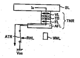
図17は、磁気トンネル接合部を有するメモリセル(以下、単に「MTJメモリセル」とも称する)の構成を示す概略図である。
【0005】
図17を参照して、MTJメモリセルは、記憶データレベルに応じて電気抵抗が変化するトンネル磁気抵抗素子TMRと、データ読出時にトンネル磁気抵抗素子TMRを通過するセンス電流Isの経路を形成するためのアクセス素子ATRとを備える。アクセス素子ATRは、代表的には電界効果型トランジスタで形成されるので、以下においては、アクセス素子ATRをアクセストランジスタATRとも称する。アクセストランジスタATRは、トンネル磁気抵抗素子TMRと固定電圧(接地電圧Vss)との間に結合される。
【0006】
MTJメモリセルに対して、データ書込を指示するためのライトワード線WWLと、データ読出を実行するためのリードワード線RWLと、データ読出およびデータ書込において、記憶データのデータレベルに対応した電気信号を伝達するためのデータ線であるビット線BLとが配置される。
【0007】
図18は、MTJメモリセルからのデータ読出動作を説明する概念図である。
図18を参照して、トンネル磁気抵抗素子TMRは、固定された一定の磁化方向を有する強磁性体層(以下、単に「固定磁化層」とも称する)FLと、外部かの印加磁界に応じた方向に磁化される強磁性体層(以下、単に「自由磁化層」とも称する)VLとを有する。固定磁化層FLおよび自由磁化層VLの間には、絶縁体膜で形成されるトンネルバリア(トンネル膜)TBが設けられる。自由磁化層VLは、書込まれる記憶データのレベルに応じて、固定磁化層FLと同一方向または固定磁化層FLと反対方向に磁化される。固定磁化層FL、トンネルバリアTBおよび自由磁化層VLによって、磁気トンネル接合が形成される。
【0008】
データ読出時においては、リードワード線RWLの活性化に応じてアクセストランジスタATRがターンオンする。これにより、ビット線BL〜トンネル磁気抵抗素子TMR〜アクセストランジスタATR〜接地電圧Vssの電流経路に、センス電流Isを流すことができる。
【0009】
トンネル磁気抵抗素子TMRの電気抵抗は、固定磁化層FLおよび自由磁化層VLのそれぞれの磁化方向の相対関係に応じて変化する。具体的には、固定磁化層FLの磁化方向と、自由磁化層VLの磁化方向とが同一(平行)である場合には、両者の磁化方向が反対(反平行)方向である場合に比べてトンネル磁気抵抗素子TMRは小さくなる。
【0010】
したがって、自由磁化層VLを記憶データに応じた方向に磁化すれば、センス電流Isによってトンネル磁気抵抗素子TMRで生じる電圧変化は、記憶データレベルに応じて異なる。したがって、たとえばビット線BLを一定電圧にプリチャージした後に、トンネル磁気抵抗素子TMRにセンス電流Isを流せば、ビット線BLの電圧を検知することによって、MTJメモリセルの記憶データを読出すことができる。
【0011】
図19は、MTJメモリセルに対するデータ書込動作を説明する概念図である。
【0012】
図19を参照して、データ書込時においては、リードワード線RWLが非活性化され、アクセストランジスタATRはターンオフされる。この状態で、自由磁化層VLを書込データに応じた方向に磁化するためのデータ書込電流が、ライトワード線WWLおよびビット線BLにそれぞれ流される。自由磁化層VLの磁化方向は、ライトワード線WWLおよびビット線BLをそれぞれ流れるデータ書込電流によって決定される。
【0013】
図20は、MTJメモリセルに対するデータ書込時におけるデータ書込電流とトンネル磁気抵抗素子の磁気方向との関係を説明する概念図である。
【0014】
図20を参照して、横軸H(EA)は、トンネル磁気抵抗素子TMR内の自由磁化層VLにおいて磁化容易軸(EA:Easy Axis)方向に印加される磁界を示す。一方、縦軸H(HA)は、自由磁化層VLにおいて磁化困難軸(HA:HardAxis)方向に作用する磁界を示す。磁界H(EA)およびH(HA)は、ビット線BLおよびライトワード線WWLをそれぞれ流れる電流によって生じる2つの磁界の一方ずつにそれぞれ対応する。
【0015】
MTJメモリセルにおいては、固定磁化層FLの固定された磁化方向は、自由磁化層VLの磁化容易軸に沿っており、自由磁化層VLは、記憶データのレベル(“1”および“0”)に応じて、磁化容易軸方向に沿って、固定磁化層FLと平行(同一)あるいは反平行(反対)方向に磁化される。以下、本明細書においては、自由磁化層VLの2種類の磁化方向にそれぞれ対応するトンネル磁気抵抗素子TMRの電気抵抗をR1およびR0(ただし、R1>R0)でそれぞれ示すこととする。MTJメモリセルは、このような自由磁化層VLの2種類の磁化方向と対応させて、1ビットのデータ(“1”および“0”)を記憶することができる。
【0016】
自由磁化層VLの磁化方向は、印加される磁界H(EA)およびH(HA)の和が、図中に示されるアステロイド特性線の外側の領域に達する場合においてのみ新たに書換えることができる。すなわち、印加されたデータ書込磁界がアステロイド特性線の内側の領域に相当する強度である場合には、自由磁化層VLの磁化方向は変化しない。
【0017】
アステロイド特性線に示されるように、自由磁化層VLに対して磁化困難軸方向の磁界を印加することによって、磁化容易軸に沿った磁化方向を変化させるのに必要な磁化しきい値が下げることができる。
【0018】
図20の例のようにデータ書込時の動作点を設計した場合には、データ書込対象であるMTJメモリセルにおいて、磁化容易軸方向のデータ書込磁界は、その強度がHWRとなるように設計される。すなわち、このデータ書込磁界HWRが得られるように、ビット線BLまたはライトワード線WWLを流されるデータ書込電流の値が設計される。一般的に、データ書込磁界HWRは、磁化方向の切換えに必要なスイッチング磁界HSWと、マージン分ΔHとの和で示される。すなわち、HWR=HSW+ΔHで示される。
【0019】
MTJメモリセルの記憶データ、すなわちトンネル磁気抵抗素子TMRの磁化方向を書換えるためには、ライトワード線WWLとビット線BLとの両方に所定レベル以上のデータ書込電流を流す必要がある。これにより、トンネル磁気抵抗素子TMR中の自由磁化層VLは、磁化容易軸(EA)に沿ったデータ書込磁界の向きに応じて、固定磁化層FLと平行もしくは、反対(反平行)方向に磁化される。トンネル磁気抵抗素子TMRに一旦書込まれた磁化方向、すなわちMTJメモリセルの記憶データは、新たなデータ書込が実行されるまでの間不揮発的に保持される。
【0020】
このようにトンネル磁気抵抗素子TMRは、印加されるデータ書込磁界によって書換可能な磁化方向に応じてその電気抵抗が変化するので、トンネル磁気抵抗素子TMR中の自由磁化層VLの2通りの磁化方向と、記憶データのレベル(“1”および“0”)とそれぞれ対応付けることによって、不揮発的なデータ記憶を実行することができる。
【0021】
【発明が解決しようとする課題】
このように、MRAMデバイスにおいては、記憶データレベルの違いに対応したトンネル磁気抵抗素子TMRでの接合抵抗差である電気抵抗差ΔR=(Rmax−Rmin)を利用してデータ読出が実行される。すなわち、選択メモリセルの通過電流、すなわちセンス電流Isの検知に基づいてデータ読出が実行される。
【0022】
一般的には、データ記憶を実行するための正規のMTJメモリセルとは別に、当該選択メモリセルの比較対象となるダミーメモリセルが設けられる。これらのダミーメモリセルは、MTJメモリセルの記憶データレベルに応じた2種類の電気抵抗RmaxおよびRminの中間レベルの電気抵抗を有するように作製する必要がある。このような電気抵抗を実現するためには、ダミーメモリセルについて特別の設計および作製を行なう必要がある。ダミーメモリセルの電気抵抗が設計値通りに仕上がらなかった場合には、データ読出マージンを損なってしまう。
【0023】
また、一般的にメモリデバイスにおいては、製造歩留りを向上させるために、アドレス信号に応じてアドレス選択される複数の正規メモリセルを備えた上で、欠陥が生じた正規メモリセルを救済するための冗長構成が備えられている。このような冗長構成においては、余分に設けられたスペアメモリセルによって、区分ごとに欠陥メモリセルが置換救済される。
【0024】
MRAMデバイスにおける冗長構成においては、十分なデータ読出マージンを確保するためには、正規のMTJメモリセルのみならず上述したダミーメモリセルについても、置換救済可能な構成としておく必要がある。すなわち、ダミーメモリセルの置換をも考慮に入れて、スペアメモリセルの配置を効率的にする必要がある。
【0025】
この発明は、このような問題点を解決するためになされたものであって、この発明の目的は、データ記憶を実行する正規のMTJメモリセルおよび、データ読出時に正規のMTJメモリセルの比較対象として設けられるダミーメモリセルの両方を効率的に置換救済可能な冗長構成を備えた薄膜磁性体記憶装置を提供することである。
【0026】
【課題を解決するための手段】
請求項1記載の薄膜磁性体記憶装置は、行および列にわたって行列状に配置され、各々が磁気的に書込まれたデータに応じた電気抵抗を有する複数のメモリセルと、各々が所定の電気抵抗を有し、複数のメモリセルとの間で行および列の一方を共有して、行および列の他方を形成するように配置された複数のダミーメモリセルと、複数のメモリセルのうちの選択された1個と、複数のダミーメモリセルのうちの1個との電気抵抗差に基づいてデータ読出を行なうデータ読出回路と、複数のメモリセルおよび複数のダミーメモリセル中の不良メモリセルを、行および列の一方を単位として置換するための冗長ユニットとを備え、冗長ユニットは、行および列の一方に沿って配置される、複数の第1のスペアメモリセル、および少なくとも1個の第2のスペアメモリセルとを含み、複数の第1のスペアメモリセルは、複数のメモリセル中の不良メモリセルを置換するために、複数のメモリセルとの間で行および列の他方を共有するように配置され、第2のスペアメモリセルは、複数のダミーメモリセル中の不良メモリセルを置換するために、複数のダミーメモリセルとの間で行および列の他方を共有するように配置される。
【0027】
請求項2に記載の薄膜磁性体記憶装置は、請求項1に記載の薄膜磁性体記憶装置であって、複数のダミーメモリセルは、行を形成するように配置され、複数のダミーメモリメモリセルは、列選択結果に基づいて、データ読出回路と選択的に接続される、。
【0028】
請求項3に記載の薄膜磁性体記憶装置は、請求項1に記載の薄膜磁性体記憶装置であって、複数のダミーメモリセルは、少なくとも1つの行を形成するように配置され、薄膜磁性体記憶装置は、複数のメモリセルの行にそれぞれ対応して設けられ、行の選択に用いられる複数の第1信号線と、ダミーメモリセルの少なくとも1つの行にそれぞれ対応して設けられ、ダミーメモリセル行の選択に用いられる複数の第2信号線とをさらに備え、複数の第1のスペアメモリセルに関する行選択は、複数の第1信号線によって実行され、複数の第2のスペアメモリセルに関する行選択は、複数の第2信号線によって実行される。
【0029】
請求項4に記載の薄膜磁性体記憶装置は、請求項1に記載の薄膜磁性体記憶装置であって、複数のダミーメモリセルは、列を形成するように配置され、薄膜磁性体記憶装置は、複数のメモリセルの列にそれぞれ対応して設けられる複数のビット線と、複数のダミーメモリセルの列に対応して設けられるダミービット線とをさらに備え、複数のメモリセルの列の各々において、対応するメモリセルおよび対応する第1のスペアメモリセルは、複数のビット線のうちの対応する1本と接続され、複数のダミーメモリセルの列において、複数のダミーメモリセルおよび第2のスペアメモリセルは、ダミービット線と接続される。
【0030】
請求項5に記載の薄膜磁性体記憶装置は、行および列にわたって行列状に配置され、各々が磁気的に書込まれたデータに応じた電気抵抗を有する複数のメモリセルと、各々が各メモリセルと同様の電気抵抗特性を有し、所定レベルのデータを予め書込まれた複数のダミーメモリセルとを備え、各複数のダミーメモリセルは、行および列の一方を複数のメモリセルとの間で共有して、行および列の他方を形成するように配置され、1個ずつのメモリセルおよびダミーメモリセルの少なくとも一方に対して、所定の電気抵抗を電気的に結合するための抵抗調整部と、複数のメモリセルのうちの選択された1個および抵抗調整部の合成抵抗と、複数のダミーメモリセルのうちの1個および抵抗調整部の合成抵抗との差に基づいてデータ読出を行なうデータ読出回路と、複数のメモリセルおよび複数のダミーメモリセル中の不良メモリセルを、行および列の他方を単位として置換するための冗長ユニットとを備え、冗長ユニットは、行および列の一方を複数のメモリセルおよび複数のダミーメモリセルと共有するように、行および列の他方に沿って配置された複数のスペアメモリセルを含み、各スペアメモリセルは、各メモリセルと同様の電気抵抗特性を有する。
【0031】
請求項6に記載の薄膜磁性体記憶装置は、請求項5に記載の薄膜磁性体記憶装置であって、各メモリセルは、データに応じて、第1および第2の電気抵抗の一方を有し、ダミーメモリセルは、第1の電気抵抗を有し、抵抗調整部と各ダミーメモリセルとの合成抵抗は、抵抗調整部と各メモリセルとのデータに応じた2通りの合成抵抗の中間値である。
【0032】
請求項7に記載の薄膜磁性体記憶装置は、請求項6に記載の薄膜磁性体記憶装置であって、記第1の電気抵抗は、第2の電気抵抗よりも小さい。
【0033】
請求項8に記載の薄膜磁性体記憶装置は、請求項5に記載の薄膜磁性体記憶装置であって、複数のダミーメモリセルおよび複数のスペアメモリセルは、行をそれぞれ形成するように配置され、薄膜磁性体記憶装置は、不良メモリセルを示す不良アドレスとアクセス対象を示すためのアドレス入力との比較に応じて、複数のメモリセル、複数のダミーメモリセルおよび複数のスペアメモリセルへのアクセスを制御するための冗長制御回路をさらに備え、冗長制御回路は、不良メモリセルが複数のダミーメモリセル中に存在する場合には、データ読出時において不良アドレスとアドレス入力とが一致したときに、複数のダミーメモリセルの行に代えて複数のスペアメモリセルの行へのアクセスを指示する。
【0034】
請求項9に記載の薄膜磁性体記憶装置は、請求項5に記載の薄膜磁性体記憶装置であって、複数のダミーメモリセルおよび複数のスペアメモリセルは、列をそれぞれ形成するように配置され、薄膜磁性体記憶装置は、データ読出時に、データ読出回路と電気的に結合される第1および第2のデータ線と、複数のメモリセルの列にそれぞれ対応して設けられ、選択されたメモリセルと第1のデータ線とを接続するための複数の第1の選択ゲートと、複数のダミーメモリセルの列に対応して設けられ、複数のダミーメモリセルのうちの1個と第2のデータ線とを接続するための複数の第2の選択ゲートと、複数のスペアメモリセルのうちの1個を第1のデータと接続するために設けられた第1のスペア選択ゲートと、複数のスペアメモリセルのうちの1個を第1のデータと接続するために設けられた第2のスペア選択ゲートとをさらに備え、第1および第2のスペア選択ゲートは、データ読出時にいて、不良メモリセルを示す不良アドレスとアクセス対象を示すためのアドレス入力とが一致した場合に、不良メモリセルが複数のメモリセルおよび複数のダミーメモリセルのいずれの中に存在するかに応じて相補的にオン・オフする。
【0035】
請求項10に記載の薄膜磁性体記憶装置は、mビット(m:2以上の整数)のデータを並列に入出力可能な薄膜磁性体記憶装置であって、各々が、行および列にわたって行列状に配置された複数のメモリセルと、列を複数のメモリセルと共有してダミーメモリセル行を形成するように配置された複数のダミーメモリセルとを含む複数のブロックを備え、各メモリセルは、磁気的に書込まれたデータに応じた電気抵抗を有し、各複数のダミーメモリセルは、所定の電気抵抗を有し、各グループは、複数のメモリセルおよび複数のダミーメモリセルによって構成された(m+1)個のメモリセル列と、(m+1)個のメモリセル列にそれぞれ対応して設けられ、相補の第1および第2のデータ線から構成される(m+1)個のデータ線対とをさらに含み、各第1および第2のデータ線は、対応するブロックからのデータ読出時において、対応するメモリセル列に属するメモリセルの1個およびダミーメモリセルのうちの1個の一方ずつとそれぞれ接続され、薄膜磁性体記憶装置は、外部との間でデータを授受するためのm個のデータ端子と、選択されたブロック中のメモリセルおよびダミーメモリセルに不良が存在する場合に、選択されたブロックにおいて、不良を接続されたデータ線対を除くm個のデータ線対を用いて、m個のデータ端子で授受されたデータを読出および書込するためのシフトリダンダンシ回路とをさらに備える。
【0036】
請求項11に記載の薄膜磁性体記憶装置は、請求項10に記載の薄膜磁性体記憶装置であって、シフトリダンダンシ回路は、選択されたブロックの(m+1)個のデータ線対にそれぞれ対応するように設けられる(m+1)個のデータノードと、(m+1)個のデータノードにそれぞれ対応して設けられ、各々が、対応するデータノードと対応するデータ線対に接続されたメモリセルとの間でデータ読出およびデータ書込を実行するためのデータ読出書込回路と、m個のデータ端子とそれぞれ対応するように設けられ、(m+1)個のデータノードの隣接する2個ずつの間にそれぞれ配置されたm個のシフトスイッチと、不良を含むブロックを示す不良アドレスと複数のブロックを選択するためのアドレス入力とを比較するための冗長制御回路とを含み、m個のシフトスイッチの接続は、冗長制御回路での比較に基づいて、選択されたブロックにおいて、不良を有するメモリセルまたはダミーメモリセルと接続されたデータ線対を除くm個のデータ線対とm個のデータ端子とをそれぞれ順に接続するように制御される。
【0037】
請求項12に記載の薄膜磁性体記憶装置は、各々が磁気的に書込まれたデータに応じた電気抵抗を有する複数のメモリセルと、各々が所定の電気抵抗を有する複数のダミーメモリセルと、所定のデータ読出電流の供給を受けて、通常のデータ読出時に複数のメモリセルのうちの1個および複数のダミーメモリセルのうちの1個の一方ずつとそれぞれ接続される第1および第2のデータ線と、第1および第2のデータ線の電圧差に基づいてデータ読出を行なうデータ読出回路とを備え、テスト時に、第1および第2のデータ線の一方のデータ線は、複数のダミーメモリセルのうちの1個と接続され、テスト時に、第1および第2のデータ線の他方のデータ線に対して、複数のメモリセルのうちの1個に代えて接続されるダミー基準電位発生部をさらに備え、ダミー基準電位発生部は、所定の電気抵抗が接続された状態での一方のデータ線の電位とは異なる電位を他方のデータ線へ印加する。
【0038】
請求項13に記載の薄膜磁性体記憶装置は、請求項12に記載の薄膜磁性体記憶装置であって、各メモリセルは、データに応じて、第1および第2の電気抵抗の一方を有し、ダミー基準電位発生部は、抵抗素子と、テスト時にオンして抵抗素子にデータ読出電流を通過させるためのスイッチ素子とを含み、スイッチ素子のオン時における、抵抗素子およびスイッチ素子の電気抵抗は、第1および第2の電気抵抗のいずれかに相当する。
【0039】
【発明の実施の形態】
以下において、本発明の実施の形態について図面を参照して詳しく説明する。
【0040】
[実施の形態1]
図1は、本発明の実施の形態に従うMRAMデバイス1の全体構成を示す概略ブロック図である。
【0041】
図1は、本発明の実施の形態に従うMRAMデバイス1の全体構成を示す概略ブロック図である。
【0042】
図1を参照して、MRAMデバイス1は、外部からの制御信号CMDおよびアドレス信号ADDに応じてランダムアクセスを実行し、書込データDINの入力および読出データDOUTの出力を実行する。MRAMデバイス1におけるデータ読出動作およびデータ書込動作は、たとえば、外部からのクロック信号CLKに同期したタイミングで実行される。あるいは、外部からクロック信号CLKを受けることなく、内部で動作タイミングを定めてもよい。
【0043】
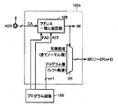
MRAMデバイス1は、アドレス信号ADDの入力を受けるアドレス端子2と、制御信号CMDおよびクロック信号CLKの入力を受ける制御信号端子3と、プログラム動作時に活性化されるプログラム信号PRGの入力を受ける信号端子4aと、制御信号CMDおよびクロック信号CLKに応答してMRAMデバイス1の全体動作を制御するためのコントロール回路5と、行列状に配置された複数のMTJメモリセルを有するメモリアレイ10とを備える。
【0044】
メモリアレイ10の構成については、後ほど詳細に説明するが、メモリアレイ10は、アドレス信号ADDによってアドレス選択可能な、行列状に配置された複数の正規のMTJメモリセル(以下、単に、「正規メモリセル」とも称する)と、アクセス対象としてアドレス選択された正規メモリセル(以下「選択メモリセル」とも称する)とのデータ読出時における比較対象として設けられた複数のダミーメモリセルと、不良が生じた正規メモリセルまたはダミーメモリセル(以下、共通に「不良メモリセル」とも称する)を所定の冗長救済区分を単位として置換救済するための冗長回路(図示せず)がさらに配置される。一般的に、冗長救済区分は、行単位、列単位、あるいはデータI/O線単位に設定される。これらの場合において、各冗長回路は、冗長ロウ、冗長コラムあるいはスペアI/O線に対応する冗長ブロックとにそれぞれ相当する。
【0045】
ダミーメモリセルは、行および列の一方を正規メモリセル列と共有するように配置される。以下においては、正規メモリセルのみで構成された行、および正規メモリセルおよびダミーメモリセルによって共有された行の両方を、総括的に「メモリセル行」と称することとする。同様に、正規メモリセルのみで構成された列、および正規メモリセルおよびダミーメモリセルによって共有された列のいずれについても総括的に、「メモリセル行」と称することとする。
【0046】
メモリセル行にそれぞれ対応して複数のライトワード線およびリードワード線RWLが配置される。また、メモリセル列にそれぞれ対応して、ビット線対を構成する相補のビット線BLおよび/BLが配置される。
【0047】
MRAMデバイス1は、さらに、行デコーダ20と、列デコーダ25と、ワード線ドライバ30と、読出/書込制御回路50,60とを備える。
【0048】
行デコーダ20は、アドレス信号ADDによって示されるロウアドレスRAに応じて、メモリアレイ10における行選択を実行する。列デコーダ25は、アドレス信号ADDによって示されるコラムアドレスCAに応じて、メモリアレイ10における列選択を実行する。ワード線ドライバ30は、行デコーダ20の行選択結果に基づいて、リードワード線RWLもしくはライトワード線WWLを選択的に活性化する。ロウアドレスRAおよびコラムアドレスCAによって、データ読出もしくはデータ書込対象に選択されたメモリセル(以下、「選択メモリセル」とも称する)が示される。
【0049】
ライトワード線WWLは、ワード線ドライバ30が配置されるのとメモリアレイ10を挟んで反対側の領域40において、接地電圧Vssと結合される。読出/書込制御回路50,60は、データ読出およびデータ書込時において、選択メモリセルに対応するメモリセル列(以下、「選択列」とも称する)のビット線BLおよび/BLに対してデータ書込電流およびセンス電流(データ読出電流)を流すために、メモリアレイ10に隣接する領域に配置される回路群を総称したものである。
【0050】
MRAMデバイス1は、さらに、プログラム回路100と、冗長制御回路105とを備える。プログラム回路100は、不良メモリセルを特定するための不良アドレスをプログラム情報として不揮発的に保持する。当該不良アドレスは、たとえば、不良メモリセルが存在するメモリセル行(以下、「不良ロウ」とも称する)を示すロウアドレス、または不良メモリセルが存在するメモリセル列(以下、「不良コラム」とも称する)を示すコラムアドレスに相当する。
【0051】
これらの不良アドレスは、アドレス信号ADDに基づくアクセスが要求されるデータ書込時およびデータ読出時において、コントロール回路5からの指示に基づいて読出され、冗長制御回路105へ伝達される。冗長制御回路105は、プログラム回路100から伝達された不良アドレスと、アドレス端子に入力されたアドレス信号ADDとの一致比較を行なう。なお、プログラム回路100および冗長制御回路105の機能を行デコーダ20または列デコーダ25に内包する構成とすることもできる。
【0052】
以下、実施の形態1においては、冗長コラムによってメモリセル列を置換単位とした冗長救済が行なわれる構成について説明する。
【0053】
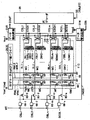
図2は、メモリアレイにおける正規メモリセル、ダミーメモリセルおよびスペアメモリセルの配置を詳細に説明する回路図である。
【0054】
図2を参照して、メモリアレイ10は、行列状に配置された複数のメモリセルMCと、複数のダミーメモリセルDMCと、冗長コラム11Cとを含む。各正規メモリセルMCの構成は、図17で説明したのと同様であり、その電気抵抗は、磁気的に書込まれたデータに応じて、RmaxおよびRminのいずれかに設定されている。
【0055】
複数のダミーメモリセルDMCは、正規メモリセルMCとメモリセル列を共有して、2個のダミーメモリセル行を形成するように行方向に沿って配置される。各ダミーメモリセルDMCは、ダミー抵抗素子TMRdおよびダミーアクセストランジスタATRdとを有する。選択時、すなわちダミーアクセストランジスタATRdのターンオン時における各ダミーメモリセルDMCは、所定の電気抵抗を有する。具体的には、選択時におけるダミーメモリセルの電気抵抗は、正規メモリセルの2種類の電気抵抗RmaxおよびRminの中間レベル、好ましくは、Rmin+ΔR/2に設定される。
【0056】
たとえば、ダミー抵抗素子TMRdを、正規メモリセルMC内のトンネル磁気抵抗素子TMRと同様の設計とし、かつ電気抵抗Rminに対応する記憶データを予め書込んだ上で、ダミーアクセストランジスタATRdのトランジスタサイズをアクセストランジスタATRと異ならせたり、ダミー抵抗素子TMRdの電気抵抗を特定値に設計することによって、このような特性のダミーメモリセルDMCが実現される。ダミーメモリセルDMCに対しては、その電気抵抗を所定値に維持される必要があるので、通常動作時のデータ書込は実行されない。
【0057】
冗長コラム11Cは、列方向に沿って配置されたスペアメモリセルSMCおよびスペアダミーメモリセルSDMCを有する。スペアメモリセルSMCは、各々が正規メモリセルMCと同様の構成および特性を有し、正規メモリセルMCとメモリセル行を共有するように配置される。スペアダミーメモリセルSDMCは、各々がダミーメモリセルDMCと同様の構成および特性を有し、ダミーメモリセルDMCとダミーメモリセル行を共有するように配置される。
【0058】
メモリアレイ10においては、正規メモリセルMCおよびスペアメモリセルSMCにおいて共有される複数のメモリセル行にそれぞれ対応してリードワード線RWLおよびライトワード線WWLが配置され、ダミーメモリセルDMCおよびスペアダミーメモリセルSDMCによって共有される2個のダミーメモリセル行にそれぞれ対応して、ダミーリードワード線DRWL0およびDRWL1が設けられる。したがって、同一のメモリセル行に属する正規メモリセルMCおよびスペアメモリセルSMCは、共通のリードワード線RWL(データ読出時)およびライトワード線WWL(データ書込時)によって選択され、同一のダミーメモリセル行に属するダミーメモリセルDMCおよびスペアダミーメモリセルSDMCは、データ読出時に、共通のダミーリードワード線DRWL0またはDRWL1によって選択される。
【0059】
さらに、正規メモリセルMCおよびダミーメモリセルDMCによって共有されるm個(m:自然数)のメモリセル列にそれぞれ対応して、相補のビット線BLおよび/BLが配置され、冗長コラム11Cに対応して、相補のスペアビット線SBLおよび/SBLが設けられる。
【0060】
以下においては、ライトワード線、リードワード線およびビット線のそれぞれを総括的に表現する場合には、符号WWL、RWLおよびBL(/BL)をそれぞれ用いて表記することとし、特定のライトワード線、リードワード線およびビット線を示す場合には、これら符号に添え字を付して、WWL1、RWL1およびBL1(/BL1)のように表記するものとする。また、信号および信号線の高電圧状態(電源電圧Vcc1,Vcc2)および低電圧状態(接地電圧Vss)のそれぞれを、単に「Hレベル」および「Lレベル」とも称する。
【0061】
正規メモリセルMCは、1行ごとにビット線BLおよび/BLのいずれか一方と接続される。たとえば、第1番目のメモリセル列に属する正規メモリセルについて説明すれば、第1行目の正規メモリセルは、ビット線BLと結合され、第2行目の正規メモリセルはビット線/BL1と結合され、以下同様に、正規メモリセルおよびスペアメモリセルの各々は、奇数行において一方のビット線BL1〜BLmと接続され、偶数行において、他方のビット線/BL1〜/BLmと接続される。
【0062】
ダミーメモリセルDMCは、ダミーリードワード線DRWL0およびDRWL1のいずれか一方と対応するように、2行×m列に配置される。ダミーリードワード線DRWL0によって選択されるダミーメモリセルは、ビット線BL1〜BLmとそれぞれ結合される。一方、ダミーリードワード線DRWL1によって選択される残りのダミーメモリセルは、ビット線/BL1〜/BLmとそれぞれ結合される。
【0063】
正規メモリセルMCと同様に、スペアメモリセルSMCは、奇数行においてスペアビット線SBLと接続され、偶数行において、スペアビット線/SBLと接続される。同様に、ダミーリードワード線DRWL0およびDRWL1によってそれぞれ選択されるスペアダミーメモリセルSDMCは、スペアビット線SBLおよび/SBLとそれぞれ接続される。
【0064】
図2においては、第1番目および第m番目のメモリセル列および第1番目および第2番目のメモリセル行に対応するリードワード線RWL1,RWL2、ライトワード線WWL1,WWL2、ビット線BL1,/BL1,BLm,/BLmが代表的に示されるが、その他のメモリセルおよびメモリセル列においても、同様の構成が設けられている。
【0065】
データ読出時において、ワード線ドライバ30は、行選択結果に応じて、各リードワード線RWLおよびダミーリードワード線DRWL0,DRWL1を選択的にHレベル(電源電圧Vcc1)に活性化する。具体的には、奇数行が選択されて、選択行の正規メモリセルおよびスペアメモリセルがビット線BL1〜BLmおよびスペアビット線SBLと接続される場合には、ダミーリードワード線DRWL1がさらに活性化されて、ダミーメモリセルDMC群およびスペアダミーメモリセルSDMCが、ビット線/BL1〜/BLmおよびスペアビット線/SBL1〜/SBLkと接続される。反対に、偶数行が選択される場合には、選択行のリードワード線に加えて、ダミーリードワード線DRWL0が活性化される。
【0066】
ワード線ドライバ30は、データ書込時において、選択行のライトワード線WWLの一端を、電源電圧Vcc2と結合する。これにより、選択行のライトワード線WWL上に、ワード線ドライバ30から領域40へ向かう方向に、行方向のデータ書込電流Ipを流すことができる。一方、非選択行のライトワード線は、ワード線ドライバ30によって、接地電圧Vssと結合される。
【0067】
メモリセル列にそれぞれ対応して、列選択を実行するためのコラム選択線CSL1〜CSLmが設けられる。さらに、冗長コラム11Cに対応して、スペアコラム選択線SCSLが配置される。列デコーダ25は、コラムアドレスCAのデコード結果、すなわち列選択結果に応じて、データ書込およびデータ読出時の各々において、コラム選択線CSL1〜CSLmおよびスペアコラム選択線SCSLの1本を選択的に活性化(Hレベルへ)する。なお、列選択の詳細については、後程詳細に説明する。
【0068】
さらに、メモリアレイ10の周辺部において、相補のデータバスDBおよび/DBが配置される。また、図1に示した読出/書込制御回路50は、データ書込回路51Wと、データ読出回路51Rと、メモリセル列にそれぞれ対応して設けられるコラム選択ゲートCSG1〜CSGmと、冗長コラム11Cに対応して設けられるスペアコラム選択ゲートSCSGとを含む。以下においては、コラム選択線CSL1〜CSLmおよびコラム選択ゲートCSG1〜CSGmをそれぞれ総称して、単に、コラム選択線CSLおよびコラム選択ゲートCSGとも称する。
【0069】
各コラム選択ゲートCSGは、データバスDBと対応するビット線BLとの間に電気的に結合されるトランジスタスイッチと、データバス/DBと対応するビット線/BLとの間に電気的に結合されるトランジスタスイッチとを有する。これらのトランジスタスイッチは、対応するコラム選択線CSLの電圧に応じてオン・オフする。すなわち、対応するコラム選択線CSLが選択状態(Hレベル)に活性化された場合には、各コラム選択ゲートCSGは、データバスDBおよび/DBを、対応するビット線BLおよび/BLのそれぞれと電気的に結合する。
【0070】
スペアコラム選択ゲートSCSGも、コラム選択ゲートCSGと同様の構成を有し、スペアコラム選択線SCSLが選択状態(Hレベル)に活性化された場合に、スペアビット線SBLおよび/SBLを、データバスDBおよび/DBのそれぞれと電気的に結合する。
【0071】
次に、MRAMデバイス1における列選択動作を説明する。列選択動作には不良コラムを置換救済するための冗長制御が含まれる。
【0072】
図3は、図1に示された冗長制御回路105の構成を示すブロック図である。図3では、一例として、不良アドレスFADは、正規メモリセルMCおよびダミーメモリセルDMCの少なくとも一方に不良メモリセルが存在する不良コラムを示す(i+1)ビット(i:自然数)で構成されるものとする。なお、不良アドレスFADについて、そのうちの1ビットを特定するときは不良アドレスビットFAD<0>のように表記することとする。また、複数ビットをまとめて示すときには、不良アドレスビットFAD<0:i>のように表記することとする。この場合、FAD<0:i>は、FAD<0>〜FAD<i>を総括的に示している。本明細書において、同様の表記は、コラムアドレスCA,ロウアドレスRA等の複数ビットから構成される他の信号にも適用される。
【0073】
図3を参照して、アドレス端子2には、不良アドレスビットFAD<0:i>と対応するコラムアドレスCAが入力される。コラムアドレスCAは、コラムアドレスビットCA<0>〜CA<i>を含む。
【0074】
冗長制御回路105は、コラムアドレスビットCA<0>〜CA<i>にそれぞれ対応して設けられた一致比較ゲート107−0〜107−iと、論理ゲート108および109とを含む。プログラム回路100は、冗長制御回路105に対して、不良アドレスビットFAD<0:i>から構成される不良アドレスFADおよび冗長コラム活性化信号ACTを与える。冗長コラム活性化信号ACTは、不良メモリセルを置換救済するために冗長コラムの使用が指示される場合に、プログラム回路100に不揮発的に記憶された情報に基づいて、Hレベルに設定される。一方、正規メモリセルおよびダミーメモリセル中に不良メモリセルが存在しない場合には、冗長コラム活性化信号ACTはLレベルに維持される。
【0075】
一致比較ゲート107−0〜107−iは、コラムアドレスCA<0:i>と不良アドレスFAD<0:i>の間で一致比較を実行する。たとえば、一致比較ゲート107−0は、コラムアドレスビットCA<0>および不良アドレスビットFAD<0>を比較して、両者が一致する場合にHレベルの信号を出力し、両者が不一致の場合にはLレベルの信号を出力する。論理ゲート108は、一致比較ゲート107−0〜107−iのそれぞれの出力間のAND演算結果を出力する。論理ゲート109は、論理ゲート108の出力とプログラム回路100からの冗長コラム活性化信号ACTとのAND論理演算結果を、スペアイネーブル信号SEとして出力する。
【0076】
したがって、論理ゲート108の出力は、コラムアドレスビットCA<0:i>と不良アドレスビットFAD<0:i>とが完全に一致した場合、すなわちコラムアドレスCAと不良アドレスFADとが完全に一致したにHレベルに設定される。また、論理ゲート109から出力するスペアイネーブル信号SEは、当該冗長コラムの使用が指示されて、かつ不良アドレスFADおよびコラムアドレスCAが一致した場合にHレベルに設定される。
【0077】
図示しないが、スペアイネーブル信号SEの反転信号はノーマルイネーブル信号として列デコーダ25へ伝達される。列デコーダ25は、ノーマルイネーブル信号がHレベルへ設定された場合には、コラムアドレスCAに基づいてコラム選択線CSL1〜CSLmの1本をHレベルへ活性化し、スペアコラム選択線SCSLはLレベルに非活性化する。これに対して、ノーマルイネーブル信号がLレベルへ設定された場合には、列デコーダ25は、スペアイネーブル信号SEに応答してスペアコラム選択線SCSLをHレベルへ活性化するとともに、各コラム選択線CSL1〜CSLmをLレベルへ非活性化する。
【0078】
再び図2を参照して、メモリセル列にそれぞれ対応して、対応するビット線BLおよび/BLの他端側同士の間を短絡するためのトランジスタスイッチ62と、トランジスタスイッチ62のオン・オフを制御する制御ゲート66とが配置される。図2においては、ビット線BL1,/BL1およびBLm,/BLmにそれぞれ対応するトランジスタスイッチ62−1および62−mと、対応する制御ゲート66−1および66−mとが代表的に示される。各トランジスタスイッチ62のゲートには、対応する制御ゲート66の出力が入力される。各制御ゲート66は、対応するメモリセル列のコラム選択線CSLの電圧レベルと、データ書込動作時にHレベルに活性化される制御信号WEとのAND論理演算結果を出力する。
【0079】
同様の構成が、冗長コラム11Cに対応して設けられる。すなわち、スペアビット線SBLおよび/SBLの他端側の間には、トランジスタスイッチ62−sが設けられ、トランジスタスイッチ62−sのゲートには、制御ゲート66−sの出力が与えられる。制御ゲート66−sは、スペアコラム選択線SCSLおよび制御信号WEの電圧レベルのAND論理演算結果を出力する。
【0080】
したがって、データ書込動作時には、コラムアドレスCAに対応する選択列もしくは冗長コラム11Cにおいて、ビット線BLおよび/BLまたは、スペアビット線SBLおよび/SBLの一端同士は、トランジスタスイッチ62によって電気的に結合される。
【0081】
また、各ビット線BL,/BLおよび各スペアビット線SBL,/SBLは、図示しないプリチャージスイッチによって、MRAMデバイス1のアクティブ期間において、少なくともデータ読出実行前の所定期間において、接地電圧Vssにプリチャージされる。一方、MRAMデバイス1のアクティブ期間のうちのデータ読出動作時およびデータ書込動作時においては、当該プリチャージスイッチはオフされて、各ビット線BL,/BLおよび各スペアビット線SBL,/SBLは、接地電圧Vss(プリチャージ電圧)から切離される。
【0082】
図4は、MRAMデバイスにおける置換救済を説明するためのデータ読出動作およびデータ書込動作時の動作波形図である。
【0083】
まず、データ書込時の動作について説明する。ワード線ドライバ30は、行デコーダ20の行選択結果に応じて、選択行に対応するライトワード線WWLを活性化して、電源電圧Vcc2と接続する。これにより、選択行のライトワード線WWLには、ワード線ドライバ30から領域40に向かう方向にデータ書込電流Ipが流される。一方、非選択行においては、ライトワード線WWLは非活性状態(Lレベル:接地電圧Vss)に維持されるので、データ書込電流は流れない。
【0084】
コラムアドレスCAが不良アドレスFADと一致しない場合には、選択列のコラム選択線CSLが選択状態(Hレベル)に活性化されて、選択列のビット線BLおよび/BLの一端ずつは、データバスDBおよび/DBとそれぞれ結合される。さらに、対応するトランジスタスイッチ62がターンオンして、選択列のビット線BLおよび/BLの他端(コラム選択ゲートCSGの反対側)同士を短絡する。
【0085】
一方、コラムアドレスCAが不良アドレスFADと一致した場合には、スペアコラム選択線SCSLが選択状態(Hレベル)に活性化されて、選択列のビット線BLおよび/BLに代えて、対応するスペアビット線SBLおよび/SBLの一端ずつが、データバスDBおよび/DBとそれぞれ結合される。さらに、トランジスタスイッチ62−sがターンオンして、対応するスペアビット線SBLおよび/SBLの他端(スペアコラム選択ゲートSCSGの反対側)同士を短絡する。
【0086】
データ書込回路51Wは、データバスDBおよび/DBを、電源電圧Vcc2(Hレベル)および接地電圧Vss(Lレベル)のいずれか一方ずつに設定する。たとえば、書込データDINのデータレベルがLレベルである場合には、データバスDBにLレベルデータを書込むためのデータ書込電流−Iwが流される。データ書込電流−Iwは、コラム選択ゲートCSGまたはスペアコラム選択ゲートSCSGを介して、選択列のビット線BLまたは対応するスペアビット線SBLに供給される。
【0087】
選択列のビット線BLまたは対応するスペアビット線SBLに流されるデータ書込電流−Iwは、ターンオンしたトランジスタスイッチ62によって折返される。これにより、他方のビット線/BLまたはスペアビット線/SBLにおいては、反対方向のデータ書込電流+Iwが流される。ビット線/BLまたはスペアビット線/SBLを流れるデータ書込電流+Iwは、コラム選択ゲートCSGまたはスペアコラム選択ゲートSCSGを介してデータバス/DBに伝達される。
【0088】
書込データDINのデータレベルがHレベルである場合には、データバスDBおよび/DBの電圧設定を入換えることによって、反対方向のデータ書込電流を、選択列のビット線BL,/BLまたは対応するスペアビット線SBL,/SBLに流すことができる。
【0089】
これにより、コラムアドレスCAが不良アドレスFADと一致しない場合には、対応するライトワード線WWLおよびビット線BL(/BL)の両方にデータ書込電流が流された正規メモリセル(選択メモリセル)がアクセス対象とされて、当該選択メモリセルへのデータ書込が実行される。一方、コラムアドレスCAが不良アドレスFADと一致した場合には、上記選択メモリセルと同一メモリセル行に属するスペアメモリセルSMCがアクセス対象とされる。すなわち、対応するライトワード線WWLおよびスペアビット線SBL(/SBL)の両方にデータ書込電流を流すことによって、スペアメモリセルSMCへのデータ書込が実行される。
【0090】
データ書込時においては、リードワード線RWLおよびダミーリードワード線DRWL0,DRWL1は非選択状態(Lレベル)に維持される。
【0091】
次に、データ読出動作について説明する。
データ読出時において、ワード線ドライバ30は、行デコーダ20の行選択結果に応じて、選択行に対応するリードワード線RWLをHレベルに活性化する。非選択行においては、リードワード線RWLの電圧レベルは非活性状態(Lレベル)に維持される。さらに、既に説明したように、選択行が偶数行および奇数行のいずれであるかに応じて、ダミーリードワード線DRWL0,DRWL1の一方が、選択行のリードワード線RWLと同様のタイミングでHレベルへ活性化される。
【0092】
データ読出が開始され、選択行のリードワード線RWLがHレベルに活性化されて、対応するアクセストランジスタATRがターンオンすると、選択行に対応する正規メモリセルMCおよびスペアメモリセルSMCは、アクセストランジスタATRを介して、ビット線BL,/BLおよびスペアビット線SBL,/SBLと、接地電圧Vssとの間に電気的に結合される。
【0093】
データ読出回路51Rは、データバスDBおよび/DBの各々を、電源電圧Vcc1でプルアップして、一定のセンス電流Isを供給する。
【0094】
さらに、データ書込時と同様に、コラムアドレスCAに応じて、選択列のコラム選択線CSLまたは、対応するスペアコラム選択線SCSLが選択的に活性化(Hレベル)される。
【0095】
コラムアドレスCAが不良アドレスFADと一致しない場合には、選択列のコラム選択線CSLの活性化に応答して、選択メモリセル(正規メモリセル)および選択メモリセルと同一メモリセル列に属するダミーメモリセルDMCのうちの1個がアクセス対象として、選択列のビット線BLおよび/BLの一方ずつを介して、データバスDBおよび/DBの一方ずつと接続される。データ読出回路51Rからのセンス電流Isによって、選択列のビット線BLおよび/BLの一方およびデータバスDB,/DBの一方には、トンネル磁気抵抗素子TMRの電気抵抗(Rmax,Rmin)、すなわち選択メモリセル記憶データのレベルに応じた電圧変化が生じる。同様に、選択列のビット線BL,/BLの他方およびデータバスDB,/DBの他方には、選択メモリセルと同一のメモリセル列に属するダミーメモリセルDMCの中間的な電気抵抗に応じた電圧変化が生じる。
【0096】
たとえば、選択メモリセルの記憶データが、電気抵抗Rmaxに対応するレベルである場合には、選択メモリセルと結合されたビット線BLおよび/BLの一方には、ダミーメモリセルDMCと結合されたビット線BLおよび/BLの他方に生じる電圧変化ΔVmよりも大きい電圧変化ΔV1(ΔV1>ΔVm)が生じる。同様に、データバスDB,/DBにおいても、電圧変化ΔVb1およびΔVbmが生じる(ΔVbm>ΔVb1)。このようにして生じたデータバスDBおよび/DBの間の電圧差をデータ読出回路51Rによって検知増幅して、選択メモリセルの記憶データを読出データDOUTとして出力することができる。
【0097】
一方、コラムアドレスCAが不良アドレスFADと一致した場合には、選択列のコラム選択線CSLに代えてスペアコラム選択線SCSLが活性化される。この結果、選択メモリセル(正規メモリセル)に代えて、選択メモリセルと同一メモリセル行に属するスペアメモリセルSMCがアクセス対象として、スペアビット線SBLおよび/SBLの一方を介して、データバスDBおよび/DBの一方と接続される。
【0098】
同様に、選択列のダミーメモリセルDMCに代えて、当該ダミーメモリセルと同一ダミーメモリセル行に属するスペアダミーメモリセルSDMCがアクセス対象とされる。当該スペアダミーメモリセルSDMCは、当該ダミーメモリセルと共通のダミーリードワード線DRWL0もしくはDRWL1の活性化に応答してスペアビット線SBLおよび/SBLの他方と接続されて、センス電流Isを受ける。
【0099】
このように、スペアメモリセルSMCおよびスペアダミーメモリセルSDMCは、正規メモリセルMCおよびダミーメモリセルDMCとの間で、メモリセル行およびダミーメモリセル行をそれぞれ共有しているので、共通のリードワード線RWL,ライトワード線WWL、およびダミーリードワード線DRWL0,DRWL1を用いて、スペアメモリセルSMCおよびスペアダミーメモリセルSDMCの行選択をも実行できる。すなわち、冗長コラム11C中において、スペアメモリセルSMCおよびスペアダミーメモリセルSDMCを選択するための専用の構成は不要となっている。
【0100】
データ読出回路51Rからセンス電流Isを同様に供給することによって、スペアビット線SBLおよび/SBLの一方およびデータバスDB,/DBの一方には、選択メモリセルに対応するスペアメモリセルの記憶データ(電気抵抗Rmax,Rmin)に応じた電圧変化が生じる。また、スペアビット線SBL,/SBLの当該他方およびデータバスDB,/DBの他方には、ダミーメモリセルDMCがアクセス対象であるときと同様の電圧変化(ΔVm,ΔVbm)が生じる。
【0101】
このように、コラムアドレスCAによって不良コラムが選択された場合でも、冗長コラム11Cに配置された、スペアメモリセルSMCおよびスペアダミーメモリセルSDMCをアクセス対象として、データ書込およびデータ読出を正常に実行できる。すなわち、冗長コラム11Cによって、不良メモリセルをメモリセル列単位で置換救済することができる。
【0102】
なお、図4において、ビット線BL,/BLおよびスペアビット線SBL,/SBLのプリチャージ電圧を接地電圧Vssとしているので、非選択列において、選択行のリードワード線RWLが活性化に応答してターンオンしたアクセストランジスタを介して、ビット線BL,/BLおよびスペアビット線SBL,/SBLから放電電流が生じることがない。この結果、プリチャージ動作時のビット線およびサブビット線の充放電による消費電力を削減できる。
【0103】
また、データ書込回路51Wの動作電源電圧であるVcc2は、データ読出回路51Rの動作電源電圧であるVcc1よりも高く設定される。データ書込時において、選択メモリセルのトンネル磁気抵抗素子TMRを磁化するために必要なデータ書込電流Ip、±Iwは、データ読出に必要なセンス電流Isよりも大きいからである。たとえば、電源電圧Vcc2には、MRAMデバイス1外部から供給される外部電源電圧をそのまま適用し、さらに、この外部電源電圧を図示しない電圧降下回路によって降下させて、電源電圧Vcc1を発生する構成とすれば、上記のこれらの電源電圧Vcc1およびVcc2を効率的に供給することができる。
【0104】
以上説明したように、実施の形態1に従う構成においては、ダミーメモリセルDMCの配置方向(行方向)と、スペアメモリセルSMCおよびスペアダミーメモリセルSDMCの配置方向(列方向)とが異なっているので、スペアメモリセルSMCおよびスペアダミーメモリセルSDMCの両方を含む冗長コラム11Cによって、正規メモリセルMCのみならずダミーメモリセルDMCについても、メモリセル列単位で不良を置換救済できる。
【0105】
言換えれば、ダミーメモリセル行が形成されるメモリアレイ配置において、メモリセル行単位で置換救済する構成とすれば、上述したスペアメモリセルSMCおよびスペアダミーメモリセルSDMCのそれぞれについて独立の冗長ロウおよび、当該冗長ロウをそれぞれ選択するための独立の信号配線を設ける必要が生じる。特に、図2に示したように折返し型ビット線構成を採用した場合には、ダミーメモリセル行を置換するための2個の冗長ロウが必要となってしまうが、冗長コラム11Cによって、正規メモリセルMCおよびダミーメモリセルDMCの両方を置換救済可能な構成とすることにより、スペアメモリセルSMCおよびスペアダミーメモリセルSDMCの配置面積を削減して、メモリアレイの小面積化を図ることができる。
【0106】
[実施の形態1の変形例1]
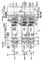
図5は、実施の形態1の変形例1に従うメモリアレイの構成を示す回路図である。
【0107】
図5を参照して、実施の形態1の変形例1に従う構成においては、図2に示した実施の形態1に従うメモリアレイ構成と比較して、ダミーメモリセルDMCが、各メモリセル列ごとに1個ずつ配置される点が異なる。各メモリセル列において、正規メモリセルMCは、ビット線BL1,BL2,…BLmに接続され、ダミーメモリセルDMCが、もう一方のビット線/BL1,/BL2,…/BLmと固定的に接続される。
【0108】
さらに、ダミーリードワード線DRWL0およびDRWL1の配置が省略され、ダミーメモリセルDMCの選択もコラム選択線CSL1〜CSLmによって実行される。すなわち、各ダミーメモリセルDMCにおいて、ダミーアクセストランジスタATRdのゲートは、対応するコラム選択線CSLと接続される。
【0109】
冗長コラム11Cにおいても、正規メモリセルMCを置換するためのスペアメモリセルSMCはスペアビット線SBLと接続され、ダミーメモリセルDMCを置換するためのスペアダミーメモリセルSDMCはスペアビット線/SBLと接続される。スペアダミーメモリセルSDMCは、スペアコラム選択線SCSLによって選択される。
【0110】
実施の形態1の変形例1に従う構成においては、さらに、データ書込を実行するための、反転ライトデータバス/WDBが備えられるとともに、トランジスタスイッチ62−1〜62−m,62−sに代えて、トランジスタスイッチ63−1〜63−m,63−sがそれぞれ設けられる。ビット線BL1〜BLmの各々は、トランジスタスイッチ63−1〜63−mをそれぞれ介して、反転ライトデータバス/WDBと接続される。スペアビット線SBLは、トランジスタスイッチ63−sを介して反転ライトデータバス/WDBと接続される。
【0111】
トランジスタスイッチ63−1〜63−m,63−sのオン・オフは、トランジスタスイッチ62−1〜62−mと同様に、制御ゲート66−1〜66−m,66−sによってそれぞれ制御される。以下においては、トランジスタスイッチ63−1〜63−mを総称して、単にトランジスタスイッチ63とも称する。その他の部分の構成および動作は、実施の形態1と同様であるので、詳細な説明は繰り返さない。
【0112】
データ書込において、選択列が不良メモリセルを含むか否かに応じて、選択列のコラム選択線CSLおよびスペアコラム選択線SCSLの一方が選択的に活性化される。
【0113】
これに応じて、選択列が不良メモリセルを含まない場合には、選択列において、対応するコラム選択ゲートCSGおよびトランジスタスイッチ63がターンオンする。この結果、選択列のビット線BLは、データバスDBおよび反転ライトデータバス/WDBの間に電気的に結合される。これに対して、選択列が不良メモリセルを含む場合には、活性化されたスペアイネーブル信号SEに応答して、スペアコラム選択線SCSLが活性化されて、トランジスタスイッチ63−sおよびスペアコラム選択ゲートSCSGがターンオンして、スペアビット線SBLは、データバスDBおよび反転ライトデータバス/WDBの間に接続される。
【0114】
この状態で、データ書込回路51Wは、図4で説明したのと同様に、書込データDINに応じて、データバスDBおよび反転ライトデータバス/WDBを、電源電圧Vcc2(Hレベル)および接地電圧Vss(Lレベル)の一方ずつに設定する。
【0115】
データ読出時においては、トランジスタスイッチ63−1〜63−m,63−sの各々がターンオフされる。さらに、選択列が不良メモリセルを含むか否かに応じて、選択列のコラム選択線CSLおよびスペアコラム選択線SCSLの一方が選択的に活性化される。
【0116】
この結果、選択列が不良メモリセルを含まない場合には、選択列のビット線BLおよび/BLを介して、選択メモリセルおよび対応するダミーメモリセルが、データバスDBおよび/DBとそれぞれ接続される。これに対して、選択列が不良メモリセルを含む場合には、スペアビット線SBLおよび/SBLを介して、選択メモリセルと同一メモリセル行のスペアメモリセルSMCおよびスペアダミーメモリセルSDMCが、データバスDBおよび/DBとそれぞれ接続される。
【0117】
この状態で、データ読出回路51Rは、図4で説明したのと同様に、データバスDBおよび/DBへセンス電流Isを供給するとともに、データバスDBおよび/DB間の電圧差に応じて読出データDOUTを生成する。
【0118】
したがって、実施の形態1の変形例1に従う構成においても、正規メモリセルMCに対応するメモリセル列と同様の構成を有する冗長コラム11Cを用いて、正規メモリセルMCおよびダミーメモリセルDMCの両方について置換救済を実行できる。
【0119】
特に、実施の形態1の変形例1に従う構成においては、ダミーメモリセルDMCおよびスペアダミーメモリセルSDMCを列選択結果に基づいて選択しているので、非選択メモリセル列および非使用時の冗長コラム11Cにおいて、ダミーメモリセルDMCおよびスペアダミーメモリセルSDMCへの無用な通過電流の発生を防止して、消費電力の低減および高速動作化を図ることができる。また、同一のメモリセル列に配置された各正規メモリセルMC(またはスペアメモリセルSMC)と比較して相対的にアクセス頻度の高いダミーメモリセルDMC(またはスペアダミーメモリセルSDMC)について、不要なアクセスを回避して動作信頼性の向上を図ることもできる。
【0120】
[実施の形態1の変形例2]
図6は、実施の形態1の変形例2に従うメモリアレイ構成を示す回路図である。
【0121】
図6を参照して、実施の形態1の変形例2に従う構成においては、図2に示した実施の形態1に従うメモリアレイ構成と比較して、ダミーリードワード線DRWL0およびDRWL1に代えて、ダミーセル選択ゲートDCG1,/DCG1〜DCGm,/DCGmおよびスペアダミーセル選択ゲートDCGs,/DCGsが配置される点で異なる。
【0122】
ダミーセル選択ゲートDCG1〜DCGmは、ビット線/BL1〜/BLmに接続されるダミーメモリセルDMCにそれぞれ対応して設けられ、スペアダミーセル選択ゲートDCGsは、スペアビット線/SBLに接続されるスペアダミーメモリセルSDMCに対応して設けられる。同様に、ダミーセル選択ゲート/DCG1〜/DCGmは、ビット線BL1〜BLmに接続されるダミーメモリセルDMCにそれぞれ対応して設けられ、スペアダミーセル選択ゲート/DCGsは、スペアビット線SBLに接続されるスペアダミーメモリセルSDMCに対応して設けられる。
【0123】
以下においては、ダミーセル選択ゲートDCG1〜DCGmを総称して単にダミーセル選択ゲートDCGとも称し、ダミーセル選択ゲート/DCG1〜/DCGmを総称して単にダミーセル選択ゲート/DCGとも称する。
【0124】
ダミーセル選択ゲートDCGの各々は、奇数行の選択時にHレベルに設定される制御信号RA0と,対応するコラム選択線CSLとのAND論理演算結果を、対応するダミーメモリセルDMC中のダミーアクセストランジスタATRdのゲートに出力する。一方、ダミーセル選択ゲート/DCGは、偶数行の選択時にHレベルに設定される制御信号/RA0(RA0の反転信号)と,対応するコラム選択線CSLとのAND論理演算結果を、対応するダミーメモリセルDMC中のダミーアクセストランジスタATRdのゲートに出力する。その他の部分の構成および動作は、実施の形態1と同様であるので、詳細な説明は繰り返さない。
【0125】
このような構成とすることにより、データ読出時には、ダミーメモリセルDMCおよびスペアダミーメモリセルSDMCを列選択結果に基づいて選択した上で、選択メモリセル(または対応するスペアメモリセル)およびダミーメモリセルDMC(またはスペアダミーメモリセルSDMC)に対して、冗長制御を反映したアクセスを実行することができる。
【0126】
したがって、実施の形態1の変形例2に従う構成と同様に、非選択メモリセル列および非使用時の冗長コラム11Cにおける、ダミーメモリセルDMCおよびスペアダミーメモリセルSDMCへの無用な通過電流の発生を防止して、消費電力低減、高速動作化、ならびにダミーメモリセルDMCおよびスペアダミーメモリセルSDMC)の動作信頼性向上を図ることもできる。
【0127】
[実施の形態1の変形例3]
図7は、実施の形態1の変形例3に従うメモリアレイ構成を示す回路図である。
【0128】
図7を参照して、実施の形態1の変形例3に従う構成においては、メモリアレイ10は、2つのメモリブロックMBaおよびMBbに分割される。メモリブロックMBaおよびMBbの各々は、m個の正規メモリセル列と、冗長コラム11Cとを有する。
【0129】
メモリブロックMBaにおいて、m個の正規メモリセル列にそれぞれ対応してビット線BL1〜BLmがそれぞれ配置され、冗長コラム11Cに対応してスペアビット線SBLが配置される。ダミーメモリセルDMCは、メモリセル列ごとに配置され、ビット線BL1〜BLmとそれぞれ接続される。
【0130】
冗長コラム11Cは、列方向に沿って配置された、正規メモリセルMCを置換救済するためのスペアメモリセルSMCおよびダミーメモリセルDMCを置換救済するためのスペアダミーメモリセルSDMCを有する。スペアメモリセルSMCは、正規メモリセルMCとメモリセル行を共有するように配置され、スペアダミーメモリセルSDMCは、ダミーメモリセルDMCと同一のダミーメモリセル行を形成するように配置される。冗長コラム11Cにおいて、スペアメモリセルSMCおよびスペアダミーメモリセルSDMCは、スペアビット線SBLと接続される。
【0131】
ビット線BL1〜BLmおよびスペアビット線SBLは、コラム選択ゲートCSGa1〜CSGamおよびスペアコラム選択ゲートSCSGaをそれぞれ介して、データバスDBと接続される。
【0132】
正規メモリセルMCとスペアメモリセルSMCとで共有されるメモリセル行にそれぞれ対応して、リードワード線RWLa1,RWLa2,…およびライトワード線WWLa1,WWLa2,…が配置される。一方、複数のダミーメモリセルDMCおよびスペアダミーメモリセルSDMCを選択する構成として、メモリセル列にそれぞれ対応するダミー選択ゲートDSGa1〜DSGamおよび、冗長コラム11Cに対応するスペアダミー選択ゲートDSGsaが設けられる。
【0133】
メモリブロックMBbもメモリブロックMBaと同様の構成を有する。すなわち、メモリブロックMBbにおいては、m個の正規メモリセル列にそれぞれ対応してビット線/BL1〜/BLmがそれぞれ配置され、冗長コラム11Cに対応してスペアビット線/SBLが配置される。ダミーメモリセルDMCは、メモリセル列ごとに配置され、ビット線/BL1〜/BLmとそれぞれ接続される。冗長コラム11Cにおいて、スペアメモリセルSMCおよびスペアダミーメモリセルSDMCは、スペアビット線/SBLと接続される。ビット線/BL1〜/BLmおよびスペアビット線/SBLは、コラム選択ゲートCSGb1〜CSGbmおよびスペアコラム選択ゲートをそれぞれ介して、データバス/DBと接続される。
【0134】
さらに、メモリブロックMBbには、正規メモリセルMCとスペアメモリセルSMCとで共有されるメモリセル行にそれぞれ対応して、リードワード線RWLb1,RWLb2,…およびライトワード線WWLb1,WWLb2,…が配置される。また、複数のダミーメモリセルDMCおよびスペアダミーメモリセルSDMCを選択するために、メモリセル列にそれぞれ対応するダミー選択ゲートDSG1b〜DSGmbおよび、冗長コラム11Cに対応するスペアダミー選択ゲートDSGsbが設けられる。
【0135】
コラム選択線CSL1〜CSLmおよびスペアコラム選択線SCSLは、メモリブロックMBaおよびMBbで共有されるように、列方向に沿って配置される。コラム選択ゲートCSGa1〜CSGamおよびCSGb1〜CSGbmは、対応するコラム選択線CSL1〜CSLmに応答してオン・オフし、スペアコラム選択ゲートSCSGa,SCSGbは、スペアコラム選択線SCSLに応答してオン・オフする。
【0136】
メモリブロックMBa中のダミー選択ゲートDSG1a〜DSGmaは、メモリブロックMBbの選択時にHレベルに活性化されるアドレスビットRAxと、対応するコラム選択線CSL1〜CSLmとのAND論理演算結果を、対応するダミーメモリセルDMC中のダミーアクセストランジスタATRdのゲートに入力する。同様に、メモリブロックMBa中のスペアダミー選択ゲートDSGsaは、アドレスビットRAxおよびスペアコラム選択線SCSLのAND論理演算結果を、対応するスペアダミーメモリセルSDMC中のダミーアクセストランジスタATRdのゲートに入力する。
【0137】
同様に、メモリブロックMBb中のダミー選択ゲートDSG1b〜DSGmbは、メモリブロックMBaの選択時にHレベルに活性化されるアドレスビット/RAx(RAxの反転信号)と対応するコラム選択線CSL1〜CSLmとのAND論理演算結果を、対応するダミーメモリセルDMC中のダミーアクセストランジスタATRdのゲートに入力する。同様に、メモリブロックMBb中のスペアダミー選択ゲートDSGsbは、アドレスビット/RAxおよびスペアコラム選択線SCSLのAND論理演算結果を、対応するスペアダミーメモリセルSDMC中のダミーアクセストランジスタATRdのゲートに入力する。
【0138】
なお、図7においては、ダミーメモリセルDMCおよびスペアダミーメモリセルSDMCの配置を主に説明するために、データ読出に関連する回路のみを記載しているが、データ書込関連回路についても、各メモリブロックにおいて図5と同様の構成が設けられているものとする。
【0139】
次に、データ読出時における動作を説明する。ここでは、一例として、選択メモリセルがメモリブロックMBaに含まれる場合について説明する。
【0140】
データ読出時において、選択メモリセル列が不良メモリセル列を含まないときには、選択列のコラム選択線CSLの活性化に応答して、メモリブロックMBaでは、選択列のビット線BLを介して選択メモリセルがデータバスDBと接続される。一方、メモリブロックMBbにおいては、選択メモリセル列のビット線/BLを介して、ダミーメモリセルDMCがデータバス/DBと接続される。
【0141】
これに対して、選択メモリセル列が不良メモリセル列を含んでいる場合には、当該選択列に対応するコラム選択線CSLに代えて、スペアコラム選択線SCSLが活性化されるので、メモリブロックMBaでは、スペアビット線SBLを介してスペアメモリセルSMCがデータバスDBと接続され、メモリブロックMBbでは、スペアビット線/SBLを介して、スペアダミーメモリセルSDMCがデータバス/DBと接続される。
【0142】
この状態で、データバスDBおよび/DBにデータ読出回路51Rからセンス電流を供給し、データバスDBおよび/DB間の電圧差を検知することによって、選択メモリセルからのデータ読出を実行することができる。
【0143】
なお、選択メモリセルがメモリブロックMBbに含まれる場合には、データバスDBおよび/DBへの接続関係が上記と入れ替わる。このようにして、メモリブロックに分割されたメモリアレイ構成においても、正規メモリセルMCおよびダミーメモリセルDMCの両方を各メモリブロックに配置された冗長コラム11Cによって置換救済して、実施の形態1およびその変形例1および2と同様の効果を享受することができる。
【0144】
[実施の形態2]
実施の形態2においては、ダミーメモリセルが正規メモリセルと同様の構成および特性を有するように設計された場合における、ダミーメモリセルの効率的な置換方式について説明する。
【0145】
図8は、実施の形態2に従うメモリアレイ構成および当該メモリアレイからのデータ読出構成を示す回路図である。
【0146】
図8を参照して、実施の形態2に従う構成においては、図2に示したメモリアレイ構成と同様に、正規メモリセルMCおよびダミーメモリセルDMC#が折返し型ビット線構成に基づいて1行ごとに交互配置される。すなわち、図8に示した構成においては、図2に示された正規メモリセルMCおよびダミーメモリセルDMCの配置において、ダミーメモリセルDMCに代えてダミーメモリセルDMC#がダミーメモリセル行を形成するように配置されている。ダミーメモリセルDMC#は、正規メモリセルMCと同様の構成および形状を有するので、同一のメモリアレイ内に連続的に作製されたMTJメモリセルの一部を用いて構成できる。すなわち、ダミーメモリセルを作製するために特別の設計や製造工程を必要としないため、構造の複雑化によるチップ面積の増大およびメモリアレイの加工マージンの低下等といった問題を招くことがない。ダミーメモリセルDMC#は、所定の電気抵抗、たとえばRminを有するような方向に予め磁化される。
【0147】
実施の形態2に従う構成においては、正規メモリセルMCと同様の特性を有するダミーメモリセルを参照してデータ読出を行なうために、データバスDBおよび/DBとデータ読出回路51Rとの間に抵抗調整部200がさらに設けられる。
【0148】
抵抗調整部200は、接続切換回路210と、ダミー抵抗220とを有する。ダミー抵抗220は、センス入力ノード/Nsiに対して直列に接続される。ダミー抵抗220の電気抵抗は、実施の形態1およびその変形例におけるダミーメモリセルDMCの電気抵抗と、Rminとの差(好ましくはΔR/2)に相当する。たとえば、ダミー抵抗220を、ゲートに可変の制御電圧Vrdが与えられたMOSトランジスタで構成することにより、それ電気抵抗を微調整可能となる。
【0149】
接続切換回路210は、センス入力ノードNsiおよび/NsiとデータバスDBとの間に電気的にそれぞれ結合されるトランジスタスイッチ211および212と、センス入力ノードNsiおよび/Nsiとデータバス/DBとの間に電気的にそれぞれ結合されるトランジスタスイッチ213および214とを有する。トランジスタスイッチ211および214の各ゲートには、奇数行の選択時にHレベルに設定されるアドレス信号RA0が入力され、トランジスタスイッチ212および213の各ゲートには、偶数行の選択時にHレベルに設定されるアドレス信号/RA0が入力される。この結果、奇数行および偶数行選択時のいずれにおいても、センス入力ノードNsiに対して選択メモリセルが直列に接続され、センス入力ノード/Nsiに対してダミーメモリセルDMCが直列に接続される。
【0150】
したがって、データ読出時には、行選択結果にかかわらず、ダミーメモリセルDMCと抵抗調整部200との合成電気抵抗は、“Rmin+ΔR/2(ダミー抵抗220)”に設定される。一方、選択メモリセルと抵抗調整部200との合成電気抵抗は、選択メモリセルの記憶データに応じて、RmaxおよびRminのいずれかであるので、データ読出回路51Rによって、センス入力ノードNsi,/Nsiにセンス電流を供給するとともに、センス入力ノードNsi,/Nsi間の電圧差を検知することによって、選択メモリセルおよびダミーメモリセル間の電気抵抗に応じたデータ読出を実行できる。
【0151】
次に、実施の形態2に従う構成における冗長救済方式について説明する。
さらに、実施の形態2に従う構成においては、図2における冗長コラム11Cに代えて、正規メモリセル行およびダミーメモリセル行の置換救済に共用される冗長ロウ11Rが配置される。冗長ロウ11Rは、ビット線BL1〜BLmと接続されたスペアメモリセルSMCで構成されたもの(奇数行置換用)と、ビット線/BL1〜/BLmと接続されたスペアメモリセルSMCで構成されたもの(偶数行置換用)とを少なくとも1個ずつ設ける必要がある。
【0152】
各スペアメモリセルSMCは、正規メモリセルMCと同様の構成および形状を有するので、同一のメモリアレイ内に連続的に作製されたMTJメモリセルの一部を用いて構成できる。各冗長ロウ11Rに対応して、スペアリードワード線SRWLおよびスペアライトワード線SWWLが配置される。図8には、奇数行置換用および偶数行置換用の1個ずつの冗長ロウ11Rと、対応するスペアリードワード線SRWL0、SRWL1およびスペアライトワード線SWWL0,SWWL1とが示される。その他の部分の構成は、実施の形態1と同様であるので詳細な説明は繰り返さない。なお、図8においても、ダミーメモリセルDMC#およびその置換救済方式を主に説明するために、データ読出に関連する回路のみを記載しているが、データ書込関連回路についても、図2と同様の構成が設けられているものとする。
【0153】
実施の形態2に従う構成では、冗長ロウ11Rによって、正規メモリセルMCおよびダミーメモリセルDMC♯の両方を置換する必要があるので、冗長制御方式が実施の形態1とは異なってくる。
【0154】
図9は、実施の形態2に従う冗長制御回路の構成を示す回路図である。
図9を参照して、実施の形態2に従う構成においては、プログラム回路100は、正規メモリセルMCの不良行を示す不良アドレスFAD(n)と、ダミーメモリセルDMCの不良行を示す不良アドレスFAD(d)の両方を記憶可能である。ただし、1つの冗長ロウ11Rによって、スペアメモリセルSMCおよびダミーメモリセルDMC♯の両方を置換することはできないため、プログラム回路100においては、不良アドレスFAD(n)およびFAD(d)のいずれか一方のみが記憶されているものとする。不良アドレスFAD(n)が記憶されている場合、すなわち正規メモリセルMCを置換救済する必要がある場合には、冗長ロウ活性化信号ACT(d)がHレベルへ活性化される。
【0155】
これに対して、不良アドレスFAD(d)が記憶されている場合、すなわちダミーメモリセルDMCの不良を置換救済する必要がある場合には、冗長ロウ活性化信号ACT(d)がHレベルへ活性化される。なお、この場合には、各スペアメモリセルSMCに対して、ダミーメモリセルDMC#の所定の電気抵抗(Rmin)に対応した記憶データの書込を予め実行する必要がある。
【0156】
不良アドレスFAD(n)は、正規メモリセルMCの不良が存在する不良コラムを示す(j+1)ビット(i:自然数)で構成されるものとする。一方、不良アドレスFAD(d)は、2個のダミーメモリセル行のいずれに不良が存在するかを示す1ビットで構成される。
【0157】
実施の形態2に従う冗長制御回路105aは、アドレス一致比較回路120と、ダミーアドレス一致比較回路122と、論理ゲート124と、インバータ128とを含む。アドレス一致比較回路120は、図3に示した冗長制御回路105と同様の構成を有し、ロウアドレスRAおよび不良アドレスFAD(n)の間で(j+1)ビットのそれぞれにおいて一致比較を実行する。アドレス一致比較回路120は、冗長ロウ活性化信号ACT(n)が活性化(Hレベル)され、かつ、ロウアドレスRAおよび不良アドレスFAD(n)が一致したときに、スペアロウイネーブル信号SREをHレベルに活性化する。
【0158】
ダミーアドレス一致比較回路122は、ロウアドレスRA中の偶数行/奇数行のいずれが選択されたかを示すアドレスビットRA<0>(たとえば、最下位ビット)と、不良アドレスFAD(d)との一致比較を実行する。ダミーアドレス一致比較回路122は、冗長ロウ活性化信号ACT(d)が活性化(Hレベル)され、かつ、アドレスビットRA<0>と不良アドレスFAD(d)が一致したときに、スペアダミーロウイネーブル信号SDREをHレベルに活性化する。
【0159】
論理ゲート124は、スペアロウイネーブル信号SREおよびスペアダミーロウイネーブル信号SDREのOR演算結果をスペアイネーブル信号SEとして出力する。また、インバータ128は、スペアダミーロウイネーブル信号SDREを反転して、ノーマルダミーロウイネーブル信号NDREとして出力する。
【0160】
行デコーダ20は、行アドレスプリデコーダ21と、論理ゲート22とを含む。行アドレスプリデコーダ21は、ロウアドレスRAを受けて、そのプリデコード結果(複数ビット)を出力する。論理ゲート22は、行アドレスプリデコーダ21から出力されたプリデコード結果のそれぞれとスペアロウイネーブル信号SREとの間のNOR演算結果をロウデコード信号RDとして出力する。ロウデコード信号RDは、ワード線ドライバ30へ伝達されて、リードワード線RWLおよびライトワード線WWLの選択に用いられる。一方、偶数行および奇数行の選択結果を示す制御信号RA0も、ダミーリードワード線DRWL0およびDRWL1の選択を実行するために、ワード線ドライバ30へ伝達される。
【0161】
ロウデコード信号RDは、スペアロウイネーブル信号SREがHレベルに活性化されると、すなわちロウアドレスRAが不良アドレスFAD(n)と一致したときには、全ビットがLレベルに設定される。これに応じて、ワード線ドライバ30は、正規メモリセルに対応するリードワード線RWLおよびライトワード線WWLの各々を非活性化する。
【0162】
これに対して、ロウアドレスRAと不良アドレスFAD(n)とが不一致のときには、ロウデコード信号RDは、行アドレスプリデコーダ21のプリデコード結果に応じて設定されて、ワード線ドライバ30は、選択行に対応するリードワード線RWL(データ読出時)もしくはライトワード線WWL(データ書込時)が活性化される。
【0163】
ワード線ドライバ30は、さらに、スペアリードワード線SRWL1,SRWL2およびスペアライトワード線SWWL1,SWWL2の活性化を、制御信号RA0および冗長制御回路105aからのスペアロウイネーブル信号SREに基づいて制御する。具体的には、不良の正規メモリセル行を置換する場合、すなわちスペアロウイネーブル信号SREが活性化されたときには、制御信号RA0に基づいて、データ読出時にはスペアリードワード線SRWL1およびSRWL2の一方を選択的に活性化し、データ書込時にはスペアライトワード線SWWL1およびSWWL2の一方を選択的に活性化する。
【0164】
これに対して、不良のダミーメモリセル行を置換する場合、すなわちスペアダミーロウイネーブル信号SDREが活性化された場合には、データ読出時には、ロウデコード信号RDに基づいて選択行のリードワード線RWLが活性化されるとともに、ダミーリードワード線DRWL0およびDRWL1に代えて、スペアリードワード線SRWL1およびSRWL2の一方が、制御信号RA0に応じて選択的に活性化される。これに対して、データ書込時には、ダミーメモリセルDMCへのアクセスが必要ないことから、スペアライトワード線SWWL1およびSWWL2の各々が非活性化(Lレベル)されたままで、ロウデコード信号RDに基づいて選択行のライトワード線WWLが活性化される。
【0165】
このような冗長判定方式を採用することにより、正規メモリセルと同様の構成のダミーメモリセルがダミーメモリ行を形成するように配置されたメモリアレイ構成において、冗長ロウを構成するように効率的に配置されたスペアメモリセルSMCを共用して、不良の正規メモリセルMCおよびダミーメモリセルDMC#のいずれをも置換救済することができる。
【0166】
[実施の形態2の変形例1]
図10は、実施の形態2の変形例1に従うメモリアレイ構成および当該メモリアレイからのデータ読出構成を示す回路図である。
【0167】
図10を参照して、実施の形態2の変形例1に従う構成においては、図8に示した実施の形態2に従う構成と比較して、抵抗調整部200に代えて、抵抗調整部201が配置される点が異なる。抵抗調整部201は、抵抗調整部200と比較して、ダミー抵抗220がセンス入力ノードNsiに対してのみ並列に接続される点が異なる。ダミー抵抗220は、制御電圧Vrdに応じて電気抵抗Rddを有するものとする。その他の部分の構成および動作は実施の形態2と同様であるので詳細な説明は繰返さない。
【0168】
既に説明したように、センス入力ノードNsiは、接続切換回路210によって、アドレス選択結果(奇数行/偶数行の選択)にかかわらず選択メモリセル(電気抵抗RmaxまたはRmin)と電気的に結合され、センス入力ノード/Nsiは、ダミーメモリセル(電気抵抗Rmin)と直列に接続される。したがって、ダミー抵抗220の電気抵抗は、ダミーメモリセルDMC#と抵抗調整部201との合成抵抗(すなわち、ダミーメモリセルDMC#の電気抵抗Rmin)が、選択メモリセルと抵抗調整部201との合成抵抗、すなわち、2種類の電気抵抗Rmax,Rminとダミー抵抗220(Rdd)との並列接続による合成抵抗である、(Rmin//Rdd)および(Rmax//Rdd)の中間レベルとなるように設定される。したがって、このような構成としても、実施の形態2と同様の効果を享受することができる。
【0169】
[実施の形態2の変形例2]
図11は、実施の形態2の変形例2に従うメモリアレイ構成および当該メモリアレイからのデータ読出構成を示す回路図である。
【0170】
図11を参照して、実施の形態2の変形例2に従う構成においては、図8に示した実施の形態2に従う構成と比較して、抵抗調整部200に代えて、抵抗調整部202が配置される点が異なる。抵抗調整部202は、抵抗調整部200と比較して、ダミー抵抗220に代えて、センス入力ノードNsiおよび/Nsiのそれぞれに対して直列に接続されるダミー抵抗221および222を有する点が異なる。
【0171】
接続切換回路210によって、アドレス選択結果にかかわらず、ダミー抵抗221は選択メモリセルと直列に接続され、ダミー抵抗222はダミーメモリセルDMC#と直列に接続される。その他の部分の構成および動作は実施の形態2と同様であるので詳細な説明は繰返さない。
【0172】
ダミー抵抗221,222の電気抵抗は、ダミーメモリセルDMC#と抵抗調整部202(ダミー抵抗221)との合成抵抗が、選択メモリセルの2種類の電気抵抗(Rmax,Rmin)と抵抗調整部202(ダミー抵抗222)の合成抵抗との2種類の電気抵抗の中間レベルとなるように設定される。たとえば、ダミーメモリセルの電気抵抗がRminに設定されているときには、ダミー抵抗221の電気抵抗をΔR/2とし、ダミー抵抗222の電気抵抗をΔRとすれば、下記(1)式のようにして、上記の条件を満足できる。
【0173】
Rmin+ΔR/2<Rmin+ΔR<Rmax+ΔR/2 …(1)
図11には、このように設計されたダミー抵抗221および222の構成例が示される。ダミー抵抗221は、並列接続されたMOSトランジスタ223,224を有し、ダミー抵抗222は、ダミー抵抗221の半分の個数、すなわち1個の電界効果型トランジスタによって構成される。トランジスタ222〜234の各ゲートには、共通の制御電圧Vrdが入力される。これにより、ダミー抵抗221の電気抵抗をダミー抵抗221の電気抵抗の1/2に設定することができる。すなわち、ダミー抵抗222の電気抵抗がΔRとなるように制御電圧Vrdを調整すれば、これに追随して、ダミー抵抗221の電気抵抗をΔR/2に設定できる。したがって、このような構成としても、実施の形態2と同様の効果を享受することができる。
【0174】
なお、実施の形態2およびその変形例(図8、9および11)においては、ダミーメモリセルの電気抵抗がRminに予め設定される場合について説明してきた。これは、MRAMデバイスの製造工程において、メモリアレイ10の作製後に実行される、図18に示した固定磁化層FLの磁化工程を終了時において、固定磁化層FLおよび自由磁化層VLの磁化方向が揃うため、ダミーメモリセルの電気抵抗がRminになるからである。したがって、ダミーメモリセルDMC#中の電気抵抗をRmaxに設定するためには、専用の磁化工程が新たに必要となってしまう。言換えれば、ダミーメモリセルDMC#の電気抵抗をRminとすることによって、ダミーメモリセル専用の新たな磁化工程が不要となる。
【0175】
しかしながら、ダミーメモリセルDMCの電気抵抗をRmaxに予め設定する場合においても、実施の形態2およびその変形例に示す構成を適用することが可能である。このような場合には、図8および10の構成においては、ダミー抵抗220が接続されるセンス入力ノードを切換えればよく、図11の構成においては、ダミー抵抗221および222の配置を入換える構成とすれば、同様のデータ読出を実行することが可能である。
【0176】
[実施の形態3]
実施の形態3においては、実施の形態1と同様のダミーメモリセルDMCが、ダミーメモリセル列を形成するように配置されたメモリアレイ構成における、ダミーメモリセルの効率的な置換方式について説明する。
【0177】
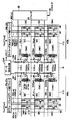
図12は、実施の形態3に従うメモリアレイ構成を示す回路図である。
図12を参照して、実施の形態3に従う構成においては、m個の正規メモリセル列と、ダミーメモリセル列とが別々に配置される。m個の正規メモリセル列およびダミーメモリセル列にそれぞれ対応して、ビット線BL1〜BLmおよびダミービット線DBLがそれぞれ配置される。
【0178】
正規メモリセルMCとダミーメモリセルDMCとはメモリセル行を共有するように配置される。すなわち、共通のリードワード線RWLおよびライトワード線WWLによって、正規メモリセルMCおよびダミーメモリセルDMCの行選択が実行される。
【0179】
さらに、これらの正規メモリセルMCおよびダミーメモリセルDMC中の不良を置換救済するために、冗長ロウ11Rが配置される。冗長ロウ11Rは、行方向に沿って配置されたスペアメモリセルSMCおよびスペアダミーメモリセルSDMCを有する。スペアメモリセルSMCは、各メモリセル列においてビット線BLと接続され、ダミーメモリ列において、スペアダミーメモリセルSDMCは、ダミービット線DBLと配置される。冗長ロウ11Rに対しては、当該冗長ロウ11Rをデータ読出時およびデータ書込時にそれぞれ選択するためのスペアリードワード線SRWLおよびスペアライトワード線SWWLが配置される。スペアメモリセルSMCおよびスペアダミーメモリセルSDMCの各ゲートは、スペアリードワード線SRWLと接続される。
【0180】
実施の形態3に従う構成においては、不良メモリセルまたは不良ダミーメモリセルの置換は、メモリセル行単位で実行される。すなわち、正規メモリセルMCおよびダミーメモリセルDMCの少なくとも一方に不良を有する不良ロウがアクセス対象に選択された場合は、当該選択行に代えて、冗長ロウ11Rがアクセス対象に指定される。すなわち、スペアリードワード線SRWL(データ読出時)またはスペアライトワード線SWWL(データ書込時)が不良ロウのリードワード線RWLまたはライトワード線WWLに代えて活性化される。この結果、不良ロウが選択されたデータ読出時には、選択列のビット線およびダミービット線DBLに対して、スペアメモリセルSMCおよびスペアダミーメモリセルSDMCをそれぞれ接続して、図2で説明したのと同様にデータ読出を実行することができる。
【0181】
また、図2と同様の、反転ライトデータバス/WDB、トランジスタスイッチ63−1〜63−mおよび制御ゲート66−1〜66−mを配置することによって、不良ロウが選択されたデータ書込時には、選択列のビット線およびスペアライトワード線SWWLにデータ書込電流を流すことによって、選択メモリセルに変えてスペアメモリセルSMCへのデータ書込を実行できる。
【0182】
以上説明したように、実施の形態3に従う構成においては、ダミーメモリセルDMCの配置方向(列方向)と、スペアメモリセルSMCおよびスペアダミーメモリセルSDMCの配置方向(行方向)とが異なっているので、スペアメモリセルSMCおよびスペアダミーメモリセルSDMCの両方を含む冗長ロウ11Rによって、正規メモリセルMCのみならずダミーメモリセルDMCについても、メモリセル行単位で不良を置換救済できる。
【0183】
言換えれば、ダミーメモリセル列が形成されるメモリアレイ配置において、メモリセル列単位で置換救済する構成とすれば、上述したスペアメモリセルSMCおよびスペアダミーメモリセルSDMCのそれぞれについて独立の冗長コラムおよび、当該冗長コラムをそれぞれ選択するための独立の信号配線を設ける必要が生じるが、冗長ロウ11Rによって、正規メモリセルMCおよびダミーメモリセルDMCの両方を置換救済可能な構成とすることにより、スペアメモリセルSMCおよびスペアダミーメモリセルSDMCの配置面積を削減して、メモリアレイの小面積化を図ることができる。
【0184】
[実施の形態4]
実施の形態4においては、正規メモリセルMCと同様の構成を有するダミーメモリセルDMC♯がダミーメモリセル列を形成するように配置されたメモリアレイ構成における、冗長救済構成について説明する。
【0185】
図13は、実施の形態4に従うメモリアレイ構成を示す回路図である。
図13を参照して、実施の形態4に従う構成においては、図12に示されたメモリアレイ構成におけるダミーメモリセルDMCに代えて、ダミーメモリセルDMC#がダミーメモリセル列を形成するように配置されている。ダミーメモリセルDMC#については、図8で説明したのと同様であるので、詳細な説明は繰り返さない。すなわち、ダミーメモリセルDMC#中は、所定の電気抵抗、たとえばRminを有するような方向に予め磁化される。
【0186】
m個の正規メモリセル列およびダミーメモリセル列にそれぞれ対応するビット線BL1〜BLmおよびダミービット線DBL、データバスDB,/DB、反転ライトデータバス/WDB、トランジスタスイッチ63−1〜63−mおよび制御ゲート66−1〜66−mについても、図12と同様に配置される。
【0187】
また、正規メモリセルMCと同様の特性を有するダミーメモリセルを参照してデータ読出を行なうために、データバス/DBに対して直列に、図8に示したダミー抵抗220が接続される。図13に示すメモリアレイ構成においては、データ読出時に、データバスDBおよび/DBは、選択メモリセルおよびダミーメモリセルと、行選択結果にかかわらず固定的にそれぞれ接続されるので、接続切換回路210の配置は不要である。
【0188】
次に、実施の形態4に従う構成における冗長救済方式について説明する。
さらに、実施の形態4に従う構成においては、図12における冗長ロウ11Rに代えて、正規メモリセル行およびダミーメモリセル行の置換救済に共用される冗長コラム11Cが配置される。冗長コラム11Cは、メモリセル行にそれぞれ対応して、列方向に沿って設けられた複数のスペアメモリセルSMCを有する。既に説明したように、各スペアメモリセルSMCは、正規メモリセルMCと同様の構成および形状を有している。
【0189】
スペアメモリセルSMCは、正規メモリセルMCおよびダミーメモリセルDMCと共有されたリードワード線RWLおよびライトワード線WWLによって選択される。各スペアメモリセルSMCは、冗長コラム11Cに対応して設けられたスペアビット線SBLと接続される。
【0190】
スペアビット線SBLは、スペアコラム選択ゲートSCSGを介してデータバスDBと接続され、スペアダミーコラム選択ゲートSDCGを介してデータバス/DBと接続される。スペアコラム選択ゲートSCSGは、スペアコラム選択線SCSLの活性化(Hレベル)に応答してオンする。スペアダミーコラム選択ゲートSDCGは、スペアダミーコラム選択線SCDSLの活性化(Hレベル)に応答してオンする。
【0191】
実施の形態4に従う構成においても、実施の形態2に従う構成と同様に、正規メモリセルMCの不良有無(図9における冗長ロウ活性化信号ACT(n)に相当)、不良メモリセルを含むメモリセル列を示す不良アドレス(図9における不良アドレスFAD(n)に相当)、およびダミーメモリセル列の不良有無(図9における冗長ロウ活性化信号ACT(d))がプログラム回路100にプログラムされる。
【0192】
そして、冗長制御回路は、図9に示したスペアロウイネーブル信号SREおよびスペアダミーロウイネーブル信号SDREに代えて、図示しないスペアコラムイネーブル信号SCEおよびスペアダミーコラムイネーブル信号SDCEを生成する。スペアコラムイネーブル信号SCEは、コラムアドレスCAが不良アドレスと一致したときにHレベルに設定され、その他ではLレベルへ非活性化される。スペアダミーコラムイネーブル信号SDCEは、ダミーメモリセルDMC#中に不良が存在し、ダミーメモリセル列を置換する必要がある場合にHレベルへ活性化される。また、スペアメモリセルSMCによるダミーメモリセルDMC#の置換救済がプログラムされる場合には、各スペアメモリセルSMCに対して、ダミーメモリセルDMC#の所定の電気抵抗(Rmin)に対応した記憶データの書込が予め実行される。
【0193】
列デコーダ25は、コラムアドレスCAならびに、冗長制御回路からのスペアコラムイネーブル信号SCEおよびスペアダミーコラムイネーブル信号SDCEに基いて、コラム選択線CSL1〜CSLm、ダミーコラム選択線DCSLおよびスペアダミーコラム選択線SCDSLを選択的に活性化(Hレベル)する。
【0194】
具体的には、不良の正規メモリセル列を置換する場合、すなわちスペアコラムイネーブル信号SCEが活性化されたときには、データ読出およびデータ書込時のそれぞれにおいて、選択列のコラム選択線に代えてダミーコラム選択線DCSLを活性化する。
【0195】
これに対して、不良のダミーメモリセル列を置換する場合、すなわちスペアダミーコラムイネーブル信号SDCEが活性化された場合には、データ読出時には、選択列のコラム選択線に代えてスペアダミーコラム選択線SDCSLが活性化される。一方、データ書込時には、ダミーメモリセルDMCへのアクセスが必要ないことから、コラムアドレスCAに基いて選択列のコラム選択線がそのまま活性化(Hレベル)される。
【0196】
このような冗長判定方式を採用することにより、ダミーメモリセルDMC#に不良が発生しても、データ読出時に、当該不良ダミーメモリセルを置換するスペアメモリセルSMCをデータバス/DBへ接続できる。また、正規メモリセルMCに不良が発生しても、データ書込およびデータ読出時のそれぞれにおいて、不良コラムの正規メモリセルMCを置換するスペアメモリセルSMCをデータバスDBへ接続できる。
【0197】
したがって、正規メモリセルと同様の構成のダミーメモリセルDMC#がダミーメモリ列を形成するように配置されたメモリアレイ構成において、冗長コラムを構成するように効率的に配置されたスペアメモリセルSMCを共用して、不良の正規メモリセルMCおよびダミーメモリセルDMC#のいずれをも置換救済することができる。
【0198】
なお、データバス/DBに対して直列に接続されるダミー抵抗220に代えて、図10と同様にデータバスDBに対して並列にダミー抵抗220を接続する構成や、図11と同様にデータバスDBおよび/DBに対してダミー抵抗221および222をそれぞれ直列に接続する構成を用いても、同様の効果を得ることができる。あるいは、実施の形態2での説明で言及したように、上述のダミー抵抗とデータバスDB、/DBとの接続関係を反対にして、電気抵抗Rmaxを有するように各ダミーメモリセルDMC#を予め磁化してもよい。
【0199】
[実施の形態5]
実施の形態5においては、シフトコラム冗長構成に基づく不良コラムの救済方式について説明する。
【0200】
図14は、実施の形態5に従うメモリアレイ構成および当該メモリアレイからのデータ読出およびデータ書込構成を示す回路図である。
【0201】
図14を参照して、実施の形態5に従う構成においては、並列にmビット(m:自然数)のデータが並列に読出または書込されるものとする。並列に入出力される書込データDIN(1)〜DIN(m)およびDOUT(1)〜DOUT(m)は、総括的に表記されたデータ端子4を構成するデータ入出力端子DP(1)〜DP(m)によって、MRAMデバイス外部と授受される。
【0202】
全体の図示は省略するが、メモリアレイ10は、各々がmビットのデータ読出あるいはデータ書込を実行するための複数のブロックに分割される。これらのブロックの各々は、(m+1)個のメモリセル列を有する。(m+1)個のメモリセル列にそれぞれ対応してビット線対BLP1〜BLPmが設けられる。ビット線対BLP1〜BLPmの各々は、相補のビット線BLおよび/BLから構成される。
【0203】
図2に示した構成と同様に、各メモリセル列において、正規メモリセルMCおよびダミーメモリセルDMCは、相補のビット線BL,/BLに対して、1行おきに交互に接続される。また、図示しないが、ビット線BLおよび/BLの一端側には、図2と同様のトランジスタスイッチ62および制御ゲート66が、各メモリセル列に対応して配置されているものとする。したがって、選択されたブロックの各メモリセル列において、データ読出時にはビット線BLおよび/BLは、選択メモリセルおよびダミーメモリセルDMCの一方ずつと接続され、データ書込時には、ビット線BLおよび/BLの当該一端同士が図示しないトランジスタスイッチによって接続される。
【0204】
なお、図14においては、選択されたブロックのみを代表的に図示している。各ブロックに対して、選択時におけるデータ読出およびデータ書込は、以下の説明と同様に実行される。
【0205】
メモリセル列単位でいわゆる「シフトリダンダンシ」を実行するために、選択ブロックの(m+1)個のメモリセル列にそれぞれ対応して、データノードNd(1)〜Nd(m+1)、リードアンプRAP(1)〜RAP(m+1)、およびライトドライバWRD(1)〜WRD(m+1)がそれぞれ設けられる。なお、以下においては、データノードNd(1)〜Nd(m+1)、リードアンプRAP(1)〜RAP(m+1)、およびライトドライバWRD(1)〜WRD(m+1)を総称して、データノードNd、リードアンプRAP、およびライトドライバWRDともそれぞれ表記する。
【0206】
各リードアンプRAPは、選択されたブロック中の対応するビット線BLおよび/BLへセンス電流を供給するとともに、当該ビット線BLおよび/BL間の電圧差に応じた読出データを対応するデータノードNdへそれぞれ生成する。
【0207】
各ライトドライバWRDは、シフトスイッチSSW(1)〜SSW(m)によって、対応するデータノードNdへ書込データが伝達された場合には、対応するビット線BLおよび/BLを書込データに応じてHレベル(電源電圧Vcc2)およびLレベル(接地電圧Vss)の一方ずつへ駆動する。この結果、対応するビット線BLおよび/BLに対して、伝達された記憶データに応じた方向のデータ書込電流を供給できる。これに対して、各ライトドライバWRDは、対応するデータノードNdへ書込データが伝達されない場合には、対応するビット線BLおよび/BLの各々をLレベル(接地電圧Vss)へ駆動する。この結果、対応するビット線BLおよび/BLに対してデータ書込電流は供給されない。
【0208】
たとえば、各ブロックの(m+1)個のビット線対と、とリードアンプRAP(1)〜RAP(m+1)およびライトドライバWRD(1)〜WRD(m+1)との間に、ブロック選択結果に応じてオン・オフする選択スイッチ(図示せず)を配置することによって、シフトリダンダンシに用いられる回路群を複数のブロック間で共有できる。
【0209】
データ入出力端子DP(1)〜DP(m)にそれぞれ対応するシフトスイッチSSW(1)〜SSW(m)は、順番に配列されたデータノードNd(1)〜Nd(m+1)の隣接する2個ずつの間にそれぞれ配置される。シフトスイッチSSW(1)〜SSW(m)の各々は、対応する2個のデータノードの一方を、データ入出力端子DP(1)〜DP(m)の対応する1つと接続する。
【0210】
シフトスイッチSSW(1)〜SSW(m)の接続方向は、冗長制御回路105bからの、冗長判定結果に基づいたシフト制御信号SF(1)〜SF(m)によってそれぞれ制御される。実施の形態5に従う構成においては、各ブロックにおいて1個余分に設けられた(m+1)個のメモリセル列を用いて、不良コラムをスキップするようにm個のメモリセル列を選択するシフトリダンダンシによって、メモリセル列を単位とする冗長救済が実行される。
【0211】
たとえば、第1番目のシフトスイッチSSW(1)は、シフト制御信号SF(1)に応じて、データノードNd(1)およびNd(2)の一方をデータ入出力端子DP(1)と選択的に接続し、第m番目(最終)の、シフトスイッチSSW(m)は、シフト制御信号SF(m)に応じて、データノードNd(m−1)およびNd(m)の一方をデータ入出力端子DP(m)と選択的に接続する。以下においては、シフトスイッチSSW(1)〜SSW(m)を総称する場合には、単にシフトスイッチSSWとも表記する。
【0212】
各シフトスイッチSSWは、不良が存在するメモリセル列に対応するデータノードNdを境に、その接続方向が変化する。たとえば、図14の構成において、第j番目(j:2〜(m+1)の自然数)のメモリセル列が不良メモリセルを含む場合には、シフトスイッチSSW(1)〜SSW(j−1)の接続方向は、ノーマル側(図14における上方向)に設定され、シフトスイッチSSW(j)〜SSW(M)の接続方向は、シフト側(図14における下方向)に設定される。また、第1番目のメモリセル列が不良メモリセル列を含む場合には、シフトスイッチSSW(1)〜SSW(m+1)の各々の接続方向は、シフト側(図14における下方向)に設定される。
【0213】
これに対して、各メモリセル列に不良コラムが存在せず、シフトリダンダンシが不要である場合には、シフトスイッチSSW(1)〜SSW(m)の各々の接続方向はノーマル側(図14における上方向)に設定される。
【0214】
図15は、実施の形態5に従う冗長制御回路の構成を示す回路図である。
図15を参照して、実施の形態5に従う構成においては、プログラム回路100は、不良コラムを含むブロックを示す不良アドレスFADと、当該ブロックの選択時に不良コラムをシフトリダンダンシによって救済するためのシフト制御信号SF(1)〜SF(m)の設定を不揮発的に記憶する。シフト制御信号SF(1)〜SF(m)は、上述したように不良コラムの位置に応じて設定される。
【0215】
冗長制御回路105bは、プログラム回路100からの不良アドレスFAD(不良コラムを示す)と、アドレス端子2に入力されたアドレスADD(ブロック選択情報)との一致比較を実行するアドレス一致比較回路120と、セレクタ125とを含む。アドレス一致比較回路120は、不良アドレスFADおよびアドレス信号ADDが一致したとき、すなわち選択されたブロックが不良コラムを含むときには、スペアイネーブル信号SEをHレベルへ活性化し、それ以外のときにはLレベルへ非活性化する。
【0216】
セレクタ125は、スペアイネーブル信号SEがHレベルに活性化されたときには、シフト制御信号SF(1)〜SF(m)をプログラム回路100でのプログラム値に基いて設定する。一方、スペアイネーブル信号SEがLレベルに活性化されているとき、すなわち選択されたブロックが不良コラムを含まないときには、各シフトスイッチSSWの接続方向がノーマル側になるように、シフト制御信号SF(1)〜SF(m)が設定される。
【0217】
このような構成とすることにより、各ブロックにおいて、余分に設けられたメモリセル列を用いたシフトリダンダンシによって、正規メモリセルMCおよびダミーメモリセルDMCの両方を、メモリセル列単位で不良を置換救済できる。なお、図14においては、図2と同様のメモリセル配置に対してシフトリダンダンシを適用する冗長構成を示したが、図5〜7と同様のメモリセル配置に対しても、シフトリダンダンシを適用することが可能である。
【0218】
[実施の形態6]
実施の形態6においては、実施の形態1〜実施の形態5において被置換対象として説明したダミーメモリセルDMC(DMC#)の不良検出を行なうためのテスト構成について説明する。
【0219】
図16は、実施の形態6に従うダミーメモリセルのテスト回路を示す回路図である。
【0220】
図16を参照して、メモリアレイ10は、図2と同様の構成を有する。したがって、通常のデータ読出時には、行選択および列選択結果に応じて、選択列のリードワード線RWL、ダミーリードワード線DRWL0またはDRWL1、および選択列のコラム選択線CSLを活性化することにより、データバスDBおよび/DBに対して、選択メモリセル(正規メモリセルMC)およびダミーメモリセルDMCの一方ずつが接続される。
【0221】
実施の形態6に従う構成においては、データバスDBおよび/DBにそれぞれ対応してダミーメモリセルDMCの不良検出のためのダミー基準電位生成回路250aおよび250bが設けられる。
【0222】
ダミー基準電位生成回路250aは、データバスDBおよび接地電圧Vssの間に直列に接続される、テストスイッチ260aおよびテスト抵抗265aを有する。テストスイッチ260aは、ゲートにテスト信号TSTaを受けるMOSトランジスタで構成される。テスト信号TSTaの活性化時において、テストスイッチ260aおよびテスト抵抗265aの電気抵抗の和が、ダミーメモリセルの不良検出テストに相応しいレベルとなるように、ダミー基準電位生成回路250aは設計される。
【0223】
ダミー基準電位生成回路250bもダミー基準電位生成回路250aと同様に設計され、データバス/DBおよび接地電圧Vssの間に直列に接続される、テストスイッチ260bおよびテスト抵抗265bを有する。
【0224】
ダミーメモリセルDMCの不良検出が実行されるテストモードにおいて、各リードワード線RWLおよびライトワード線WWLは非活性化され、ダミーリードワード線DRWL0,DRWL1の一方が活性化される。これに応答して、データバスDBおよび/DBの一方が、ダミーメモリセルDMCを介して接地電圧Vssでプルダウンされる。さらに、データバスDBおよび/DBの他方が、テスト抵抗265aまたは265bを介して接地電圧へプルダウンされるように、テスト信号TSTaおよびTSTbの一方が活性化される。
【0225】
このような構成とすることにより、たとえば、テスト信号TSTaおよびTSTbの活性化時における、ダミー基準電位生成回路250a,250bの電気抵抗が、正規メモリセルの所定電気抵抗、すなわちRmaxまたはRminとなるように設計することにより、データバスDB,/DBの一方ずつに対して、被試験対象のダミーメモリセルの電気抵抗に応じた電圧、および、ダミー基準電位生成回路250a,250bによるテスト用基準電位をそれぞれ生じさせることができる。すなわち、当該テスト用基準電位は、設計値どおりの電気抵抗を有するダミーメモリセルDMCがデータバスDB,/DBに生じさせる電位とは異なるレベルに設計されている。
【0226】
したがって、データ読出回路51RがデータバスDB,/DB間の電圧比較に基いて生成する読出データDOUTに基いて、ダミーメモリセルDMCの不良を検出できる。具体的には、ダミー基準電位生成回路250a,250bの電気抵抗と、ダミーメモリセルDMCの所定抵抗レベル(Rmin+ΔR/2)との大小関係に応じた極性を、当該読出データDOUTが有しているか否かによって、ダミーメモリセルDMCの不良を検出できる。
【0227】
なお、実施の形態6に従うダミーメモリセルのテスト構成は、特にメモリアレイ10の構成に限定されず適用することができる。すなわち、テストモード時に、ダミーメモリセルDMCを接続可能なデータ線が存在すれば、当該データ線の比較対象として、図16に示したダミー基準電位生成回路250a,250bを設けることにより、同様の効果を享受することができる。
【0228】
今回開示された実施の形態はすべての点で例示であって制限的なものではないと考えられるべきである。本発明の範囲は上記した説明ではなくて特許請求の範囲によって示され、特許請求の範囲と均等の意味および範囲内でのすべての変更が含まれることが意図される。
【0229】
【発明の効果】
請求項1に記載の薄膜磁性体記憶装置は、ダミーメモリセルの配置方向と、第1および第2のスペアメモリセルの配置方向とが異なっているので、第1および第2のスペアメモリセルの両方を含む冗長ユニットCによって、正規のメモリセルのみならずダミーメモリセルについても、メモリセル列単位で不良を置換救済できる。すなわち、第1および第2のスペアメモリセルの配置面積を削減して、メモリアレイの小面積化を図ることができる。
【0230】
請求項2に記載の薄膜磁性体記憶装置は、ダミーメモリセルを列選択結果に基づいて選択しているので、非選択メモリセル列において、ダミーメモリセルおよび第2のスペアメモリセルへの無用な通過電流の発生を防止できるので、請求項1に記載の薄膜磁性体記憶装置が奏する効果に加えて、消費電力の低減および高速動作化を図ることができる。また、同一メモリセル列に配置された正規のメモリセルまたは第1のスペアメモリセルと比較して相対的にアクセス頻度の高いダミーメモリセルまたは第2のスペアメモリセルについて、不要なアクセスを回避することで動作信頼性の向上を図ることもできる。
【0231】
請求項3および4に記載の薄膜磁性体記憶装置は、冗長ユニット中における第1および第2のスペアメモリセルを選択するための構成を新たに設ける必要がないので、請求項1に記載の薄膜磁性体記憶装置が奏する効果に加えて、メモリアレイの小面積化をさらに図ることができる。
【0232】
請求項5、6、8および9に記載の薄膜磁性体記憶装置は、メモリセルと同様の構成のダミーメモリセルが配置されたメモリアレイ構成において、スペアメモリセルによって構成される単一の冗長ユニットを用いて、不良のメモリセルおよびダミーメモリセルのいずれをも、行単位または列単位で置換救済することができる。さらに、ダミーメモリセルがメモリセルと同様の構成および形状を有するので、ダミーメモリセルを作製するために特別の設計や製造工程を必要としないため、構造の複雑化によるチップ面積の増大およびメモリアレイの加工マージンの低下等といった問題を招くことがない。
【0233】
請求項7に記載の薄膜磁性体記憶装置は、請求項6に記載の薄膜磁性体記憶装置が奏する効果に加えて、ダミーメモリセルの電気抵抗を設定するための専用の新たな磁化工程が不要となる。
【0234】
請求項10および11に記載の薄膜磁性体記憶装置は、複数ビットのデータを並列に書込・読出可能なブロックごとに、余分に設けられたメモリセル列を用いたシフトリダンダンシを実行して、メモリセルおよびダミーメモリセルの両方について、メモリセル列単位で不良を置換救済できる。したがって、多ビットを並列に入出力するメモリアレイ構成において、冗長構成を効率化できる。
【0235】
請求項12および13に記載の薄膜磁性体記憶装置は、通常動作時に用いられるデータ読出回路を共用して、テスト時にダミーメモリセルの不良を検知することができる。
【図面の簡単な説明】
【図1】本発明の実施の形態に従うMRAMデバイスの全体構成を示す概略ブロック図である。
【図2】実施の形態1に従うメモリアレイの構成を説明する回路図である。
【図3】図1に示された冗長制御回路105の構成を示すブロック図である。
【図4】MRAMデバイスにおける置換救済を説明するためのデータ読出動作およびデータ書込動作時の動作波形図である。
【図5】実施の形態1の変形例1に従うメモリアレイの構成を示す回路図である。
【図6】実施の形態1の変形例2に従うメモリアレイ構成を示す回路図である。
【図7】実施の形態1の変形例3に従うメモリアレイ構成を示す回路図である。
【図8】実施の形態2に従うメモリアレイ構成および当該メモリアレイからのデータ読出構成を示す回路図である。
【図9】実施の形態2に従う冗長制御回路の構成を示す回路図である。
【図10】実施の形態2の変形例1に従うメモリアレイ構成および当該メモリアレイからのデータ読出構成を示す回路図である。
【図11】実施の形態2の変形例2に従うメモリアレイ構成および当該メモリアレイからのデータ読出構成を示す回路図である。
【図12】実施の形態3に従うメモリアレイ構成を示す回路図である。
【図13】実施の形態4に従うメモリアレイ構成を示す回路図である。
【図14】実施の形態5に従うメモリアレイ構成および当該メモリアレイからのデータ読出およびデータ書込構成を示す回路図である。
【図15】図14に示される冗長制御回路の構成を示すブロック図である。
【図16】実施の形態6に従うダミーメモリセルのテスト回路を示す回路図である。
【図17】MTJメモリセルの構成を示す概略図である。
【図18】MTJメモリセルからのデータ読出動作を説明する概念図である。
【図19】MTJメモリセルに対するデータ書込動作を説明する概念図である。
【図20】MTJメモリセルに対するデータ書込時におけるデータ書込電流とトンネル磁気抵抗素子の磁気方向との関係を説明する概念図である。
【符号の説明】
1 MRAMデバイス、4 データ端子、10 メモリアレイ、11R 冗長ロウ、11C 冗長コラム、20 行デコーダ、25 列デコーダ、30 ワード線ドライバ、51W データ書込回路、51R データ読出回路、100 プログラム回路、105,105a,105b 冗長制御回路、200〜202 抵抗調整部、210 接続切換回路、220〜222 ダミー抵抗、250a,250b ダミー基準電位生成回路、260a,260b テストスイッチ、265a,265b テスト抵抗、BL,/BL ビット線、DB,/DB データバス、DCG,/DCG ダミーセル選択ゲート、DCGs,/DCGs スペアダミーセル選択ゲート、Nsi,/Nsi センス入力ノード、SBL,/SBL スペアビット線、/WDB 反転ライトデータバス、ADD アドレス信号、ATR アクセストランジスタ、ATRd ダミーアクセストランジスタ、BLP1〜BLPm ビット線対、CA コラムアドレス、CSG,CSGa,CSGb コラム選択ゲート、CSL コラム選択線、DBL ダミービット線、DCSL ダミーコラム選択線、DIN 書込データ、DMC ダミーメモリセル、DOUT 読出データ、DP(1)〜DP(m) データ入出力端子、DRWL0,DRWL1 ダミーリードワード線、DSG1a,DSG1b ダミー選択ゲート、DSGsa,DSGsb スペアダミー選択ゲート、FAD 不良アドレス、Ip データ書込電流、Is センス電流、MBa,MBb メモリブロック、MC メモリセル(正規メモリセル)、RA ロウアドレス、RAP リードアンプ、RD ロウデコード信号、RWL リードワード線、SBL,/SBL スペアビット線、SCDSL スペアダミーコラム選択線、SCSL スペアコラム選択線、SDMC スペアダミーメモリセル、SE スペアイネーブル信号、SF(1)〜SF(m) シフト制御信号、SMC スペアメモリセル、SRWL,SRWL0,SRWL1 スペアリードワード線、SSW(1)〜SSW(m) シフトスイッチ、SWWL,SWWL0,SWWL1 スペアライトワード線、TB トンネルバリア、TMR トンネル磁気抵抗素子、TMRd ダミー抵抗素子、WRD 各ライトドライバ、WWL ライトワード線。[0001]
TECHNICAL FIELD OF THE INVENTION
The present invention relates to a thin-film magnetic storage device, and more particularly, to a thin-film magnetic storage device having a redundant configuration.
[0002]
[Prior art]
As a storage device capable of storing nonvolatile data with low power consumption, an MRAM (Magnetic Random Access Memory) device has attracted attention. An MRAM device is a storage device that performs non-volatile data storage using a plurality of thin-film magnetic materials formed in a semiconductor integrated circuit, and enables random access to each of the thin-film magnetic materials.
[0003]
In particular, in recent years, it has been announced that the performance of an MRAM device will be drastically improved by using a thin-film magnetic material using a magnetic tunnel junction (MTJ: Magnetic Tunnel Junction) as a memory cell. For an MRAM device having a memory cell having a magnetic tunnel junction, see "A 10 ns Read and Write Non-Volatile Memory Array Using a Magnetic Tunnel Junction and FET Touch Cell Access Cell Touch Desc. . 2000. , "Nonvolatile RAM based on Magnetic Tunnel Junction Elements", ISSCC Digest of Technical Papers, TA7.3, Feb. 2000. And “A 256 kb 3.0V 1T1MTJ Nonvolatile Magnetoresistive RAM”, ISSCC Digest of Technical Papers, TA7.6, Feb. 2000. And the like.
[0004]
FIG. 17 is a schematic diagram showing a configuration of a memory cell having a magnetic tunnel junction (hereinafter, also simply referred to as “MTJ memory cell”).
[0005]
Referring to FIG. 17, the MTJ memory cell forms a path for tunneling magneto-resistance element TMR whose electric resistance changes according to the storage data level and a path for sense current Is passing through tunneling magneto-resistance element TMR during data reading. And an access element ATR. Since access element ATR is typically formed of a field effect transistor, access element ATR is also referred to as access transistor ATR below. Access transistor ATR is coupled between tunneling magneto-resistance element TMR and a fixed voltage (ground voltage Vss).
[0006]
Write word line WWL for instructing data write to MTJ memory cell, read word line RWL for executing data read, and data level corresponding to storage data in data read and data write. Bit lines BL, which are data lines for transmitting electric signals, are arranged.
[0007]
FIG. 18 is a conceptual diagram illustrating an operation of reading data from an MTJ memory cell.
Referring to FIG. 18, tunneling magneto-resistance element TMR has a fixed ferromagnetic layer FL having a fixed magnetization direction (hereinafter, also simply referred to as "fixed magnetization layer") FL and an externally applied magnetic field. And a ferromagnetic layer (hereinafter, also simply referred to as “free magnetic layer”) VL that is magnetized in the direction. A tunnel barrier (tunnel film) TB formed of an insulator film is provided between the fixed magnetic layer FL and the free magnetic layer VL. Free magnetic layer VL is magnetized in the same direction as fixed magnetic layer FL or in the opposite direction to fixed magnetic layer FL, depending on the level of the stored data to be written. A magnetic tunnel junction is formed by fixed magnetic layer FL, tunnel barrier TB, and free magnetic layer VL.
[0008]
At the time of data reading, access transistor ATR is turned on in response to activation of read word line RWL. Thus, the sense current Is can flow through the current path from the bit line BL, the tunneling magneto-resistance element TMR, the access transistor ATR, and the ground voltage Vss.
[0009]
The electric resistance of tunneling magneto-resistance element TMR changes according to the relative relationship between the magnetization directions of fixed magnetic layer FL and free magnetic layer VL. Specifically, when the magnetization direction of the fixed magnetic layer FL and the magnetization direction of the free magnetic layer VL are the same (parallel), the magnetization directions of the two are opposite (anti-parallel) as compared with the case where the magnetization directions are opposite (anti-parallel). Tunneling magneto-resistance element TMR becomes smaller.
[0010]
Therefore, if free magnetic layer VL is magnetized in the direction corresponding to the storage data, the voltage change generated in tunneling magneto-resistance element TMR by sense current Is differs according to the storage data level. Therefore, if bit line BL is precharged to a constant voltage and then sense current Is is applied to tunneling magneto-resistance element TMR, the data stored in the MTJ memory cell can be read by detecting the voltage on bit line BL. it can.
[0011]
FIG. 19 is a conceptual diagram illustrating a data write operation to an MTJ memory cell.
[0012]
Referring to FIG. 19, at the time of data writing, read word line RWL is inactivated, and access transistor ATR is turned off. In this state, a data write current for magnetizing free magnetic layer VL in a direction corresponding to the write data flows through write word line WWL and bit line BL. The magnetization direction of free magnetic layer VL is determined by the data write current flowing through write word line WWL and bit line BL, respectively.
[0013]
FIG. 20 is a conceptual diagram illustrating the relationship between the data write current and the magnetic direction of the tunnel magnetoresistive element when writing data to the MTJ memory cell.
[0014]
Referring to FIG. 20, a horizontal axis H (EA) indicates a magnetic field applied in an easy axis (EA) direction in free magnetic layer VL in tunneling magneto-resistance element TMR. On the other hand, the vertical axis H (HA) indicates a magnetic field acting in the direction of the hard axis (HA: HardAxis) in the free magnetic layer VL. Magnetic fields H (EA) and H (HA) respectively correspond to two magnetic fields generated by currents flowing through bit line BL and write word line WWL, respectively.
[0015]
In the MTJ memory cell, the fixed magnetization direction of fixed magnetic layer FL is along the easy axis of free magnetic layer VL, and free magnetic layer VL is at the level of stored data (“1” and “0”). Along the easy axis direction, the magnetization is magnetized in a direction parallel (identical) or antiparallel (opposite) to the fixed magnetization layer FL. Hereinafter, in this specification, the electric resistances of tunneling magneto-resistance element TMR corresponding to the two types of magnetization directions of free magnetic layer VL are indicated by R1 and R0 (where R1> R0). The MTJ memory cell can store 1-bit data (“1” and “0”) in correspondence with such two kinds of magnetization directions of the free magnetic layer VL.
[0016]
The magnetization direction of free magnetic layer VL can be rewritten only when the sum of applied magnetic fields H (EA) and H (HA) reaches a region outside the asteroid characteristic line shown in the figure. it can. That is, when the applied data write magnetic field has a strength corresponding to the region inside the asteroid characteristic line, the magnetization direction of free magnetic layer VL does not change.
[0017]
As shown by the asteroid characteristic line, by applying a magnetic field in the direction of the hard axis to the free magnetic layer VL, the magnetization threshold required for changing the magnetization direction along the easy axis is reduced. be able to.
[0018]
When the operating point at the time of data writing is designed as in the example of FIG. 20, in the MTJ memory cell to which data is written, the intensity of the data writing magnetic field in the easy axis direction is H. WR It is designed to be. That is, the data write magnetic field H WR Is designed so that the value of the data write current flowing through bit line BL or write word line WWL is obtained. Generally, the data write magnetic field H WR Is the switching magnetic field H required for switching the magnetization direction. SW And a margin ΔH. That is, H WR = H SW + ΔH.
[0019]
In order to rewrite the storage data of the MTJ memory cell, that is, the magnetization direction of tunneling magneto-resistance element TMR, it is necessary to flow a data write current of a predetermined level or more to both write word line WWL and bit line BL. Thereby, free magnetic layer VL in tunneling magneto-resistance element TMR is parallel or opposite (anti-parallel) to fixed magnetic layer FL, depending on the direction of the data write magnetic field along the easy axis (EA). Magnetized. The magnetization direction once written in tunneling magneto-resistance element TMR, that is, the data stored in the MTJ memory cell, is held in a nonvolatile manner until new data writing is performed.
[0020]
As described above, the tunneling magneto-resistance element TMR changes its electric resistance in accordance with the rewritable magnetization direction by the applied data write magnetic field, and thus the two magnetizations of the free magnetic layer VL in the tunneling magneto-resistance element TMR. By associating the directions with the levels (“1” and “0”) of the storage data, nonvolatile data storage can be performed.
[0021]
[Problems to be solved by the invention]
As described above, in the MRAM device, data reading is performed using the electric resistance difference ΔR = (Rmax−Rmin) which is the junction resistance difference in the tunneling magneto-resistance element TMR corresponding to the difference in the storage data level. That is, data reading is performed based on the detection of the passing current of the selected memory cell, that is, the sense current Is.
[0022]
Generally, a dummy memory cell to be compared with the selected memory cell is provided separately from a normal MTJ memory cell for executing data storage. These dummy memory cells need to be manufactured so as to have an intermediate level of electrical resistance between two types of electrical resistances Rmax and Rmin according to the storage data level of the MTJ memory cell. In order to realize such electric resistance, it is necessary to perform special design and fabrication for the dummy memory cell. If the electrical resistance of the dummy memory cell is not finished as designed, the data read margin is impaired.
[0023]
In general, a memory device includes a plurality of normal memory cells which are selected in accordance with an address signal in order to improve a manufacturing yield, and is used to repair a defective normal memory cell. A redundant configuration is provided. In such a redundant configuration, defective memory cells are replaced and remedied for each section by extra spare memory cells.
[0024]
In the redundant configuration of the MRAM device, in order to secure a sufficient data read margin, it is necessary to provide not only the normal MTJ memory cell but also the above-described dummy memory cell in a configuration capable of replacing and replacing. That is, it is necessary to efficiently arrange the spare memory cells in consideration of the replacement of the dummy memory cells.
[0025]
An object of the present invention is to solve such a problem, and an object of the present invention is to compare a normal MTJ memory cell for executing data storage and a normal MTJ memory cell for reading data. It is an object of the present invention to provide a thin-film magnetic memory device having a redundant configuration capable of efficiently replacing and relieving both dummy memory cells provided as.
[0026]
[Means for Solving the Problems]
A thin-film magnetic memory device according to
[0027]
The thin-film magnetic memory device according to
[0028]
The thin-film magnetic memory device according to
[0029]
A thin-film magnetic storage device according to a fourth aspect is the thin-film magnetic storage device according to the first aspect, wherein the plurality of dummy memory cells are arranged so as to form a column. A plurality of bit lines provided corresponding to the columns of the plurality of memory cells, and a dummy bit line provided corresponding to the columns of the plurality of dummy memory cells. , The corresponding memory cell and the corresponding first spare memory cell are connected to a corresponding one of the plurality of bit lines, and in the column of the plurality of dummy memory cells, the plurality of dummy memory cells and the second spare memory cell are connected. The memory cells are connected to dummy bit lines.
[0030]
6. A thin-film magnetic memory device according to
[0031]
A thin film magnetic memory device according to a sixth aspect is the thin film magnetic memory device according to the fifth aspect, wherein each memory cell has one of the first and second electric resistances according to data. The dummy memory cell has a first electrical resistance, and the combined resistance of the resistance adjustment unit and each of the dummy memory cells is intermediate between the two types of combined resistances according to the data of the resistance adjustment unit and each of the memory cells. Value.
[0032]
A thin-film magnetic memory device according to a seventh aspect is the thin-film magnetic memory device according to the sixth aspect, wherein the first electric resistance is smaller than the second electric resistance.
[0033]
The thin film magnetic memory device according to claim 8 is the thin film magnetic memory device according to
[0034]
A thin-film magnetic storage device according to a ninth aspect is the thin-film magnetic storage device according to the fifth aspect, wherein the plurality of dummy memory cells and the plurality of spare memory cells are arranged so as to form columns. And a thin-film magnetic memory device, which is provided corresponding to the first and second data lines electrically coupled to the data read circuit and the column of the plurality of memory cells at the time of data reading, respectively. A plurality of first selection gates for connecting the cells to the first data lines; and a plurality of first selection gates provided corresponding to the columns of the plurality of dummy memory cells, wherein one of the plurality of dummy memory cells and the second A plurality of second selection gates for connecting to the data line; a first spare selection gate provided for connecting one of the plurality of spare memory cells to the first data; Spare memory cells And a second spare selection gate provided for connecting one of the first and second data to the first data, wherein the first and second spare selection gates are at the time of data reading and have a defective address indicating a defective memory cell. When the address matches the address input for indicating the access target, the defective memory cell is turned on / off complementarily depending on which of the plurality of memory cells and the plurality of dummy memory cells exists.
[0035]
The thin-film magnetic memory device according to
[0036]
The thin film magnetic memory device according to an eleventh aspect is the thin film magnetic memory device according to the tenth aspect, wherein the shift redundancy circuit corresponds to (m + 1) data line pairs of the selected block. Provided between the (m + 1) data nodes and the (m + 1) data nodes, respectively, between each of the corresponding data nodes and the memory cells connected to the corresponding data line pair. And a data read / write circuit for executing data read and data write, respectively, and m data terminals, respectively, and are provided between two adjacent (m + 1) data nodes, respectively. A redundancy control circuit for comparing the arranged m shift switches with a defective address indicating a block including a defect and an address input for selecting a plurality of blocks. The connection of the m shift switches is based on the comparison in the redundancy control circuit, and in the selected block, the number of the m shift switches excluding the data line pair connected to the defective memory cell or the dummy memory cell is The data line pair and the m data terminals are controlled so as to be connected in order.
[0037]
The thin-film magnetic memory device according to claim 12, wherein a plurality of memory cells each having an electric resistance according to magnetically written data, and a plurality of dummy memory cells each having a predetermined electric resistance. Receiving a predetermined data read current and connecting to one of the plurality of memory cells and one of the plurality of dummy memory cells during normal data read, respectively. And a data read circuit for performing data read based on a voltage difference between the first and second data lines. During a test, one of the first and second data lines has a plurality of data lines. A dummy reference potential connected to one of the dummy memory cells and connected to the other of the first and second data lines in place of one of the plurality of memory cells during a test; Generation part Comprising the al, dummy reference voltage generating unit applies a different potential to the other data line from the potential of one of the data lines in a state in which a predetermined electric resistance is connected.
[0038]
A thin-film magnetic storage device according to a thirteenth aspect is the thin-film magnetic storage device according to the twelfth aspect, wherein each memory cell has one of the first and second electric resistances according to data. The dummy reference potential generating section includes a resistance element and a switch element that is turned on during a test to allow a data read current to pass through the resistance element, and that when the switch element is turned on, the electrical resistance of the resistance element and the switch element is reduced. Corresponds to one of the first and second electric resistances.
[0039]
BEST MODE FOR CARRYING OUT THE INVENTION
Hereinafter, embodiments of the present invention will be described in detail with reference to the drawings.
[0040]
[Embodiment 1]
FIG. 1 is a schematic block diagram showing an overall configuration of an
[0041]
FIG. 1 is a schematic block diagram showing an overall configuration of an
[0042]
Referring to FIG. 1,
[0043]
[0044]
Although the configuration of the
[0045]
The dummy memory cells are arranged such that one of the rows and columns is shared with the normal memory cell columns. In the following, both a row composed of only normal memory cells and a row shared by normal memory cells and dummy memory cells will be collectively referred to as a “memory cell row”. Similarly, a column formed only of normal memory cells and a column shared by the normal memory cells and the dummy memory cells are collectively referred to as “memory cell rows”.
[0046]
A plurality of write word lines and read word lines RWL are arranged corresponding to the respective memory cell rows. Complementary bit lines BL and / BL forming a bit line pair are arranged corresponding to the respective memory cell columns.
[0047]
The
[0048]
[0049]
Write word line WWL is coupled to ground voltage Vss in a
[0050]
The
[0051]
These defective addresses are read based on an instruction from
[0052]
Hereinafter, in the first embodiment, a description will be given of a configuration in which redundancy repair is performed using a memory cell column as a replacement unit by a redundant column.
[0053]
FIG. 2 is a circuit diagram illustrating in detail the arrangement of normal memory cells, dummy memory cells, and spare memory cells in the memory array.
[0054]
Referring to FIG. 2,
[0055]
The plurality of dummy memory cells DMC are arranged along the row direction so as to form two dummy memory cell rows, sharing a memory cell column with normal memory cells MC. Each dummy memory cell DMC has a dummy resistance element TMRd and a dummy access transistor ATRd. When selected, that is, when the dummy access transistor ATRd is turned on, each dummy memory cell DMC has a predetermined electric resistance. Specifically, the electric resistance of the dummy memory cell at the time of selection is set to an intermediate level between the two kinds of electric resistances Rmax and Rmin of the normal memory cell, preferably, Rmin + ΔR / 2.
[0056]
For example, dummy resistance element TMRd is designed in the same manner as tunneling magneto-resistance element TMR in normal memory cell MC, and after storing data corresponding to electric resistance Rmin in advance, the size of dummy access transistor ATRd is reduced. By making the resistance different from that of the access transistor ATR or designing the electric resistance of the dummy resistance element TMRd to a specific value, the dummy memory cell DMC having such characteristics is realized. Since the electrical resistance of dummy memory cell DMC needs to be maintained at a predetermined value, data writing during normal operation is not performed.
[0057]
[0058]
In
[0059]
Further, complementary bit lines BL and / BL are arranged corresponding to m (m: natural number) memory cell columns shared by normal memory cells MC and dummy memory cells DMC, respectively, and correspond to
[0060]
Hereinafter, when each of the write word line, the read word line, and the bit line is collectively expressed, the write word line, the read word line, and the bit line are represented by reference numerals WWL, RWL, and BL (/ BL). , Read word lines and bit lines are denoted by subscripts and are denoted by WWL1, RWL1, and BL1 (/ BL1). Further, the high voltage state (power supply voltages Vcc1 and Vcc2) and the low voltage state (ground voltage Vss) of the signal and the signal line, respectively, are also simply referred to as “H level” and “L level”.
[0061]
Normal memory cells MC are connected to one of bit lines BL and / BL for each row. For example, as for the normal memory cells belonging to the first memory cell column, the normal memory cells in the first row are connected to the bit line BL, and the normal memory cells in the second row are connected to the bit line / BL1. Similarly, each of the normal memory cell and the spare memory cell is connected to one bit line BL1 to BLm in an odd row, and connected to the other bit line / BL1 to / BLm in an even row.
[0062]
Dummy memory cells DMC are arranged in 2 rows × m columns so as to correspond to one of dummy read word lines DRWL0 and DRWL1. Dummy memory cells selected by dummy read word line DRWL0 are coupled to bit lines BL1 to BLm, respectively. On the other hand, the remaining dummy memory cells selected by dummy read word line DRWL1 are coupled to bit lines / BL1 to / BLm, respectively.
[0063]
Similarly to normal memory cell MC, spare memory cell SMC is connected to spare bit line SBL in an odd-numbered row and connected to spare bit line / SBL in an even-numbered row. Similarly, spare dummy memory cells SDMC selected by dummy read word lines DRWL0 and DRWL1 are connected to spare bit lines SBL and / SBL, respectively.
[0064]
In FIG. 2, read word lines RWL1, RWL2, write word lines WWL1, WWL2, bit lines BL1, / BL correspond to the first and mth memory cell columns and the first and second memory cell rows. Although BL1, BLm, and / BLm are representatively shown, similar configurations are provided in other memory cells and memory cell columns.
[0065]
At the time of data reading,
[0066]
[0067]
Column selection lines CSL1 to CSLm for executing column selection are provided corresponding to the respective memory cell columns. Further, spare column select line SCSL is arranged corresponding to
[0068]
Further, complementary data buses DB and / DB are arranged in the peripheral portion of
[0069]
Each column select gate CSG is electrically coupled between a data bus DB and a corresponding bit line BL, and is electrically coupled between a data bus / DB and a corresponding bit line / BL. Transistor switch. These transistor switches are turned on / off according to the voltage of the corresponding column selection line CSL. That is, when corresponding column select line CSL is activated to the selected state (H level), each column select gate CSG connects data buses DB and / DB to corresponding bit lines BL and / BL, respectively. Electrically coupled.
[0070]
Spare column select gate SCSG has the same structure as column select gate CSG, and sets spare bit lines SBL and / SBL to data bus when spare column select line SCSL is activated to a selected state (H level). It is electrically coupled to each of DB and / DB.
[0071]
Next, a column selecting operation in the
[0072]
FIG. 3 is a block diagram showing a configuration of
[0073]
Referring to FIG. 3, column address CA corresponding to defective address bits FAD <0: i> is input to address
[0074]
[0075]
Match comparison gates 107-0 to 107-i perform match comparison between column address CA <0: i> and defective address FAD <0: i>. For example, match comparison gate 107-0 compares column address bit CA <0> and defective address bit FAD <0> and outputs an H-level signal when they match, and outputs an H level signal when they do not match. Outputs an L level signal.
[0076]
Therefore, the output of
[0077]
Although not shown, an inverted signal of the spare enable signal SE is transmitted to the
[0078]
Referring to FIG. 2 again, a
[0079]
A similar configuration is provided corresponding to
[0080]
Therefore, at the time of data write operation, one end of bit lines BL and / BL or spare bit lines SBL and / SBL are electrically coupled by
[0081]
Further, each bit line BL, / BL and each spare bit line SBL, / SBL are precharged to the ground voltage Vss by an unillustrated precharge switch at least during a predetermined period before data reading is executed during an active period of the
[0082]
FIG. 4 is an operation waveform diagram at the time of a data read operation and a data write operation for describing replacement relief in the MRAM device.
[0083]
First, the operation at the time of data writing will be described. The
[0084]
When column address CA does not match defective address FAD, column select line CSL of the selected column is activated to a selected state (H level), and one end of each of bit lines BL and / BL of the selected column is connected to data bus. DB and / DB. Further, the corresponding
[0085]
On the other hand, when column address CA matches defective address FAD, spare column select line SCSL is activated to the selected state (H level), and the corresponding spare is selected instead of bit lines BL and / BL of the selected column. One ends of bit lines SBL and / SBL are coupled to data buses DB and / DB, respectively. Further, transistor switch 62-s is turned on, and the other ends of corresponding spare bit lines SBL and / SBL (opposite to spare column selection gate SCSG) are short-circuited.
[0086]
[0087]
The data write current -Iw flowing through the bit line BL of the selected column or the corresponding spare bit line SBL is turned back by the turned-on
[0088]
When the data level of write data DIN is at the H level, the voltage setting of data buses DB and / DB is exchanged, so that the data write current in the opposite direction can be changed to bit line BL, / BL or BL of the selected column. The current can flow to corresponding spare bit lines SBL, / SBL.
[0089]
Thus, when column address CA does not match defective address FAD, a normal memory cell (selected memory cell) in which a data write current has flowed to both corresponding write word line WWL and bit line BL (/ BL) Are to be accessed, and data writing to the selected memory cell is executed. On the other hand, when the column address CA matches the defective address FAD, the spare memory cell SMC belonging to the same memory cell row as the selected memory cell is set as an access target. That is, by writing a data write current to both the corresponding write word line WWL and spare bit line SBL (/ SBL), data writing to spare memory cell SMC is performed.
[0090]
At the time of data writing, read word line RWL and dummy read word lines DRWL0 and DRWL1 are maintained in a non-selected state (L level).
[0091]
Next, a data read operation will be described.
At the time of data reading,
[0092]
When data reading is started, read word line RWL of the selected row is activated to H level, and corresponding access transistor ATR is turned on, normal memory cell MC and spare memory cell SMC corresponding to the selected row become access transistor ATR. , Are electrically coupled between bit lines BL, / BL and spare bit lines SBL, / SBL and ground voltage Vss.
[0093]
Data read
[0094]
Further, as in the data writing, column selection line CSL of the selected column or a corresponding spare column selection line SCSL is selectively activated (H level) in accordance with column address CA.
[0095]
If the column address CA does not match the defective address FAD, the selected memory cell (normal memory cell) and the dummy memory belonging to the same memory cell column as the selected memory cell are responded to activation of the column selection line CSL of the selected column. One of the cells DMC is connected to one of the data buses DB and / DB via one of the bit lines BL and / BL of the selected column as an access target. By the sense current Is from the data read
[0096]
For example, when the storage data of the selected memory cell is at a level corresponding to electric resistance Rmax, one of bit lines BL and / BL coupled to the selected memory cell has a bit coupled to dummy memory cell DMC. A voltage change ΔV1 (ΔV1> ΔVm) larger than a voltage change ΔVm generated on the other of lines BL and / BL occurs. Similarly, voltage changes ΔVb1 and ΔVbm also occur in data buses DB and / DB (ΔVbm> ΔVb1). The voltage difference between data buses DB and / DB generated in this manner can be detected and amplified by data read
[0097]
On the other hand, when column address CA matches defective address FAD, spare column select line SCSL is activated instead of column select line CSL of the selected column. As a result, instead of the selected memory cell (normal memory cell), the spare memory cell SMC belonging to the same memory cell row as the selected memory cell is accessed and the data bus DB is connected via one of the spare bit lines SBL and / SBL. And / DB.
[0098]
Similarly, instead of the dummy memory cell DMC in the selected column, a spare dummy memory cell SDMC belonging to the same dummy memory cell row as the dummy memory cell is to be accessed. Spare dummy memory cell SDMC is connected to the other of spare bit lines SBL and / SBL in response to activation of dummy read word line DRWL0 or DRWL1 common to the dummy memory cell, and receives sense current Is.
[0099]
As described above, since the spare memory cell SMC and the spare dummy memory cell SDMC share the memory cell row and the dummy memory cell row with the normal memory cell MC and the dummy memory cell DMC, respectively, the common read word Using the line RWL, the write word line WWL, and the dummy read word lines DRWL0 and DRWL1, row selection of the spare memory cells SMC and the spare dummy memory cells SDMC can also be performed. That is, a dedicated configuration for selecting the spare memory cell SMC and the spare dummy memory cell SDMC in the
[0100]
By supplying sense current Is in the same manner from data read
[0101]
As described above, even when a defective column is selected by column address CA, data writing and data reading are normally performed with spare memory cell SMC and spare dummy memory cell SDMC arranged in
[0102]
In FIG. 4, since the precharge voltages of bit lines BL and / BL and spare bit lines SBL and / SBL are set to ground voltage Vss, the read word line RWL of the selected row responds to the activation in the non-selected columns. No discharge current is generated from the bit lines BL and / BL and the spare bit lines SBL and / SBL via the access transistor that is turned on. As a result, power consumption due to charging and discharging of the bit lines and sub-bit lines during the precharge operation can be reduced.
[0103]
Vcc2, which is the operation power supply voltage of data write
[0104]
As described above, in the configuration according to the first embodiment, the arrangement direction (row direction) of dummy memory cells DMC is different from the arrangement direction (column direction) of spare memory cells SMC and spare dummy memory cells SDMC. Therefore, with the
[0105]
In other words, in a memory array arrangement in which a dummy memory cell row is formed, if replacement and repair is performed in units of memory cell rows, independent redundant rows and spare rows are provided for each of the above-described spare memory cells SMC and spare dummy memory cells SDMC. In addition, it is necessary to provide independent signal lines for selecting the redundant rows. In particular, when a folded bit line configuration is employed as shown in FIG. 2, two redundant rows for replacing a dummy memory cell row are required. By providing both the cell MC and the dummy memory cell DMC with a configuration capable of replacing and replacing, the arrangement area of the spare memory cell SMC and the spare dummy memory cell SDMC can be reduced, and the area of the memory array can be reduced.
[0106]
[
FIG. 5 is a circuit diagram showing a configuration of the memory array according to the first modification of the first embodiment.
[0107]
Referring to FIG. 5, in the configuration according to the first modification of the first embodiment, dummy memory cells DMC are provided for each memory cell column, as compared with the memory array configuration according to the first embodiment shown in FIG. The difference is that they are arranged one by one. In each memory cell column, normal memory cells MC are connected to bit lines BL1, BL2,... BLm, and dummy memory cells DMC are fixedly connected to the other bit lines / BL1, / BL2,. You.
[0108]
Further, the arrangement of dummy read word lines DRWL0 and DRWL1 is omitted, and selection of dummy memory cells DMC is also performed by column selection lines CSL1 to CSLm. That is, in each dummy memory cell DMC, the gate of the dummy access transistor ATRd is connected to the corresponding column selection line CSL.
[0109]
Also in
[0110]
The configuration according to the first modification of the first embodiment further includes an inverted write data bus / WDB for executing data writing, and replaces transistor switches 62-1 to 62-m and 62-s. Thus, transistor switches 63-1 to 63-m and 63-s are provided, respectively. Each of bit lines BL1 to BLm is connected to inverted write data bus / WDB via transistor switches 63-1 to 63-m, respectively. Spare bit line SBL is connected to inverted write data bus / WDB via transistor switch 63-s.
[0111]
On / off of the transistor switches 63-1 to 63-m and 63-s is controlled by control gates 66-1 to 66-m and 66-s, respectively, similarly to the transistor switches 62-1 to 62-m. . Hereinafter, the transistor switches 63-1 to 63-m are collectively referred to simply as a
[0112]
In data writing, one of column selection line CSL and spare column selection line SCSL of the selected column is selectively activated according to whether or not the selected column includes a defective memory cell.
[0113]
Accordingly, when the selected column does not include a defective memory cell, the corresponding column selection gate CSG and
[0114]
In this state, data write
[0115]
At the time of data reading, each of the transistor switches 63-1 to 63-m and 63-s is turned off. Further, one of the column selection line CSL and the spare column selection line SCSL of the selected column is selectively activated according to whether or not the selected column includes a defective memory cell.
[0116]
As a result, when the selected column does not include a defective memory cell, the selected memory cell and the corresponding dummy memory cell are connected to data buses DB and / DB via bit lines BL and / BL of the selected column, respectively. You. On the other hand, when the selected column includes a defective memory cell, the spare memory cell SMC and the spare dummy memory cell SDMC in the same memory cell row as the selected memory cell are connected to via the spare bit lines SBL and / SBL. Connected to buses DB and / DB, respectively.
[0117]
In this state, data read
[0118]
Therefore, in the configuration according to the first modification of the first embodiment, both normal memory cell MC and dummy memory cell DMC are formed using
[0119]
Particularly, in the configuration according to the first modification of the first embodiment, dummy memory cell DMC and spare dummy memory cell SDMC are selected based on the result of column selection. In 11C, generation of unnecessary passing current to dummy memory cell DMC and spare dummy memory cell SDMC can be prevented, and power consumption can be reduced and high-speed operation can be achieved. In addition, unnecessary dummy memory cells DMC (or spare dummy memory cells SDMC) that are relatively frequently accessed compared to the normal memory cells MC (or spare memory cells SMC) arranged in the same memory cell column are unnecessary. Access reliability can be improved by avoiding access.
[0120]
[
FIG. 6 is a circuit diagram showing a memory array configuration according to the second modification of the first embodiment.
[0121]
Referring to FIG. 6, the configuration according to the second modification of the first embodiment differs from the memory array configuration according to the first embodiment shown in FIG. 2 in that dummy read word lines DRWL0 and DRWL1 are replaced by dummy cells. The difference is that select gates DCG1, / DCG1 to DCGm, / DCGm and spare dummy cell select gates DCGs, / DCGs are arranged.
[0122]
Dummy cell selection gates DCG1 to DCGm are provided corresponding to dummy memory cells DMC connected to bit lines / BL1 to / BLm, respectively. Spare dummy cell selection gates DCGs are provided for spare dummy memory connected to spare bit line / SBL. It is provided corresponding to cell SDMC. Similarly, dummy cell selection gates / DCG1 to / DCGm are provided corresponding to dummy memory cells DMC connected to bit lines BL1 to BLm, respectively, and spare dummy cell selection gates / DCGs are connected to spare bit line SBL. It is provided corresponding to spare dummy memory cell SDMC.
[0123]
Hereinafter, the dummy cell selection gates DCG1 to DCGm are collectively referred to simply as a dummy cell selection gate DCG, and the dummy cell selection gates / DCG1 to / DCGm are also referred to simply as a dummy cell selection gate / DCG.
[0124]
Each of the dummy cell selection gates DCG outputs an AND logical operation result between a control signal RA0 set to H level when an odd row is selected and a corresponding column selection line CSL, to a dummy access transistor ATRd in a corresponding dummy memory cell DMC. Output to the gate. On the other hand, the dummy cell selection gate / DCG stores an AND logical operation result of a control signal / RA0 (an inverted signal of RA0) set to H level when an even-numbered row is selected and a corresponding column selection line CSL in a corresponding dummy memory. Output to the gate of the dummy access transistor ATRd in the cell DMC. Other configurations and operations are the same as those in the first embodiment, and thus detailed description will not be repeated.
[0125]
With this configuration, at the time of data reading, after selecting the dummy memory cell DMC and the spare dummy memory cell SDMC based on the column selection result, the selected memory cell (or the corresponding spare memory cell) and the dummy memory cell An access reflecting the redundancy control can be executed on the DMC (or the spare dummy memory cell SDMC).
[0126]
Therefore, similarly to the configuration according to the second modification of the first embodiment, generation of unnecessary passing current to dummy memory cell DMC and spare dummy memory cell SDMC in unselected memory cell column and unused
[0127]
[Third Modification of First Embodiment]
FIG. 7 is a circuit diagram showing a memory array configuration according to a third modification of the first embodiment.
[0128]
Referring to FIG. 7, in a configuration according to the third modification of the first embodiment,
[0129]
In memory block MBa, bit lines BL1 to BLm are arranged corresponding to m normal memory cell columns, respectively, and spare bit lines SBL are arranged corresponding to
[0130]
The
[0131]
Bit lines BL1 to BLm and spare bit line SBL are connected to data bus DB via column selection gates CSGa1 to CSGam and spare column selection gate SCSGa, respectively.
[0132]
Read word lines RWLa1, RWLa2, ... and write word lines WWLa1, WWLa2, ... are arranged corresponding to memory cell rows shared by normal memory cells MC and spare memory cells SMC, respectively. On the other hand, as a configuration for selecting a plurality of dummy memory cells DMC and spare dummy memory cells SDMC, dummy select gates DSGa1 to DSGam respectively corresponding to the memory cell columns and spare dummy select gate DSGsa corresponding to
[0133]
Memory block MBb has the same configuration as memory block MBa. That is, in memory block MBb, bit lines / BL1 to / BLm are arranged corresponding to m normal memory cell columns, respectively, and spare bit line / SBL is arranged corresponding to
[0134]
Further, read word lines RWLb1, RWLb2, ... and write word lines WWLb1, WWLb2, ... are arranged in memory block MBb corresponding to memory cell rows shared by normal memory cells MC and spare memory cells SMC, respectively. Is done. In order to select a plurality of dummy memory cells DMC and spare dummy memory cells SDMC, dummy select gates DSG1b to DSGmb respectively corresponding to the memory cell columns and spare dummy select gate DSGsb corresponding to
[0135]
Column select lines CSL1 to CSLm and spare column select line SCSL are arranged along the column direction so as to be shared by memory blocks MBa and MBb. Column select gates CSGa1 to CSGam and CSGb1 to CSGbm turn on / off in response to corresponding column select lines CSL1 to CSLm, and spare column select gates SCSGa and SCSGb turn on / off in response to spare column select line SCSL. I do.
[0136]
Dummy select gates DSG1a to DSGma in memory block MBa output the AND logic operation result of address bit RAx activated to H level when memory block MBb is selected and corresponding column select lines CSL1 to CSLm, to the corresponding dummy. Input to the gate of the dummy access transistor ATRd in the memory cell DMC. Similarly, spare dummy select gate DSGsa in memory block MBa inputs the address bit RAx and the AND operation result of spare column select line SCSL to the gate of dummy access transistor ATRd in corresponding spare dummy memory cell SDMC.
[0137]
Similarly, dummy select gates DSG1b to DSGmb in memory block MBb are connected to column select lines CSL1 to CSLm corresponding to address bits / RAx (inverted signal of RAx) activated to H level when memory block MBa is selected. The result of the AND logic operation is input to the gate of dummy access transistor ATRd in corresponding dummy memory cell DMC. Similarly, spare dummy select gate DSGsb in memory block MBb inputs the address bit / RAx and the AND operation result of spare column select line SCSL to the gate of dummy access transistor ATRd in corresponding spare dummy memory cell SDMC. .
[0138]
In FIG. 7, only circuits related to data reading are shown in order to mainly explain the arrangement of dummy memory cells DMC and spare dummy memory cells SDMC. It is assumed that the same configuration as that of FIG. 5 is provided in the memory block.
[0139]
Next, an operation at the time of data reading will be described. Here, a case where the selected memory cell is included in memory block MBa will be described as an example.
[0140]
At the time of data reading, when the selected memory cell column does not include a defective memory cell column, the memory block MBa responds to the activation of the column selection line CSL of the selected column, via the bit line BL of the selected column. The cell is connected to the data bus DB. On the other hand, in memory block MBb, dummy memory cell DMC is connected to data bus / DB via bit line / BL of the selected memory cell column.
[0141]
On the other hand, when the selected memory cell column includes a defective memory cell column, the spare column selection line SCSL is activated instead of the column selection line CSL corresponding to the selected column. In MBa, spare memory cell SMC is connected to data bus DB via spare bit line SBL, and in memory block MBb, spare dummy memory cell SDMC is connected to data bus / DB via spare bit line / SBL. .
[0142]
In this state, a sense current is supplied from data read
[0143]
When the selected memory cell is included in memory block MBb, the connection relation to data buses DB and / DB is switched as described above. In this manner, even in a memory array configuration divided into memory blocks, both normal memory cells MC and dummy memory cells DMC are replaced and replaced by
[0144]
[Embodiment 2]
In the second embodiment, an efficient replacement method of a dummy memory cell when the dummy memory cell is designed to have the same configuration and characteristics as a normal memory cell will be described.
[0145]
FIG. 8 is a circuit diagram showing a memory array configuration and a configuration for reading data from the memory array according to the second embodiment.
[0146]
Referring to FIG. 8, in the configuration according to the second embodiment, similar to the memory array configuration shown in FIG. 2, normal memory cells MC and dummy memory cells DMC # are arranged for each row based on a folded bit line configuration. Are alternately arranged. That is, in the configuration shown in FIG. 8, in the arrangement of normal memory cells MC and dummy memory cells DMC shown in FIG. 2, dummy memory cells DMC # form dummy memory cell rows instead of dummy memory cells DMC. Are arranged as follows. Since the dummy memory cell DMC # has the same configuration and shape as the normal memory cell MC, it can be configured using a part of the MTJ memory cells continuously manufactured in the same memory array. That is, since no special design or manufacturing process is required to manufacture the dummy memory cell, problems such as an increase in the chip area due to a complicated structure and a reduction in the processing margin of the memory array are not caused. Dummy memory cell DMC # is magnetized in advance in a direction having a predetermined electric resistance, for example, Rmin.
[0147]
In the structure according to the second embodiment, in order to read data with reference to a dummy memory cell having the same characteristics as normal memory cell MC, resistance adjustment is performed between data buses DB and / DB and data read
[0148]
The
[0149]
[0150]
Therefore, at the time of data reading, the combined electrical resistance of dummy memory cell DMC and
[0151]
Next, a redundancy repair method in the configuration according to the second embodiment will be described.
Further, in the configuration according to the second embodiment, a
[0152]
Each spare memory cell SMC has the same configuration and shape as the regular memory cell MC, and therefore can be configured using a part of the MTJ memory cells continuously manufactured in the same memory array. A spare read word line SRWL and a spare write word line SWWL are arranged corresponding to each
[0153]
In the configuration according to the second embodiment, it is necessary to replace both normal memory cell MC and dummy memory cell DMC # with
[0154]
FIG. 9 is a circuit diagram showing a configuration of the redundancy control circuit according to the second embodiment.
Referring to FIG. 9, in the configuration according to the second embodiment,
[0155]
On the other hand, when defective address FAD (d) is stored, that is, when replacement of defective dummy memory cell DMC needs to be relieved, redundant row activation signal ACT (d) is activated to the H level. Be converted to In this case, it is necessary to previously write storage data corresponding to a predetermined electric resistance (Rmin) of dummy memory cell DMC # to each spare memory cell SMC.
[0156]
It is assumed that the defective address FAD (n) is composed of (j + 1) bits (i: natural number) indicating a defective column in which a defective normal memory cell MC exists. On the other hand, the defective address FAD (d) is composed of one bit indicating which of the two dummy memory cell rows has a defective.
[0157]
[0158]
The dummy address
[0159]
[0160]
[0161]
All bits of row decode signal RD are set to L level when spare row enable signal SRE is activated to H level, that is, when row address RA matches defective address FAD (n). In response,
[0162]
On the other hand, when the row address RA and the defective address FAD (n) do not match, the row decode signal RD is set according to the predecode result of the
[0163]
[0164]
On the other hand, when a defective dummy memory cell row is replaced, that is, when spare dummy row enable signal SDRE is activated, at the time of data reading, read word line RWL of a selected row is selected based on row decode signal RD. Is activated, and instead of dummy read word lines DRWL0 and DRWL1, one of spare read word lines SRWL1 and SRWL2 is selectively activated according to control signal RA0. On the other hand, at the time of data writing, since access to the dummy memory cell DMC is not required, each of the spare write word lines SWWL1 and SWWL2 is kept inactive (L level) and based on the row decode signal RD. Thus, the write word line WWL of the selected row is activated.
[0165]
By adopting such a redundancy determination method, it is possible to efficiently configure a redundant row in a memory array configuration in which dummy memory cells having the same configuration as normal memory cells are arranged to form a dummy memory row. By sharing the arranged spare memory cell SMC, both the defective normal memory cell MC and the dummy memory cell DMC # can be replaced and repaired.
[0166]
[
FIG. 10 is a circuit diagram showing a memory array configuration and a data read configuration from the memory array according to the first modification of the second embodiment.
[0167]
Referring to FIG. 10, in the configuration according to the first modification of the second embodiment,
[0168]
As described above, sense input node Nsi is electrically coupled to selected memory cell (electric resistance Rmax or Rmin) by
[0169]
[
FIG. 11 is a circuit diagram showing a memory array configuration and a data reading configuration from the memory array according to the second modification of the second embodiment.
[0170]
Referring to FIG. 11, in the configuration according to the second modification of the second embodiment,
[0171]
By the
[0172]
The electrical resistance of the
[0173]
Rmin + ΔR / 2 <Rmin + ΔR <Rmax + ΔR / 2 (1)
FIG. 11 shows a configuration example of the
[0174]
In the second embodiment and its modifications (FIGS. 8, 9 and 11), a case has been described where the electric resistance of the dummy memory cell is set to Rmin in advance. This is because the magnetization directions of the fixed magnetic layer FL and the free magnetic layer VL are changed when the magnetization step of the fixed magnetic layer FL shown in FIG. This is because the electrical resistance of the dummy memory cells becomes Rmin because they are aligned. Therefore, in order to set the electric resistance in the dummy memory cell DMC # to Rmax, a new dedicated magnetization step is required. In other words, by setting the electric resistance of the dummy memory cell DMC # to Rmin, a new magnetization step dedicated to the dummy memory cell is not required.
[0175]
However, even when the electric resistance of dummy memory cell DMC is set to Rmax in advance, the configurations shown in the second embodiment and its modifications can be applied. In such a case, in the configuration of FIGS. 8 and 10, the sense input node to which the
[0176]
[Embodiment 3]
In the third embodiment, an efficient replacement method of the dummy memory cells in a memory array configuration in which the same dummy memory cells DMC as in the first embodiment are arranged to form a dummy memory cell column will be described.
[0177]
FIG. 12 is a circuit diagram showing a memory array configuration according to the third embodiment.
Referring to FIG. 12, in the configuration according to the third embodiment, m normal memory cell columns and dummy memory cell columns are separately arranged. Bit lines BL1 to BLm and dummy bit line DBL are arranged corresponding to the m normal memory cell columns and the dummy memory cell columns, respectively.
[0178]
Normal memory cells MC and dummy memory cells DMC are arranged to share a memory cell row. That is, the row selection of the normal memory cell MC and the dummy memory cell DMC is executed by the common read word line RWL and write word line WWL.
[0179]
Further, a
[0180]
In the configuration according to the third embodiment, replacement of a defective memory cell or a defective dummy memory cell is performed in units of memory cell rows. That is, when a defective row having a defect in at least one of the normal memory cell MC and the dummy memory cell DMC is selected as an access target, the
[0181]
By arranging inverted write data bus / WDB, transistor switches 63-1 to 63-m and control gates 66-1 to 66-m as in FIG. 2, at the time of data writing in which a defective row is selected. By supplying a data write current to the bit line of the selected column and the spare write word line SWWL, data can be written to the spare memory cell SMC instead of the selected memory cell.
[0182]
As described above, in the configuration according to the third embodiment, the arrangement direction (column direction) of dummy memory cells DMC is different from the arrangement direction (row direction) of spare memory cells SMC and spare dummy memory cells SDMC. Therefore, with the
[0183]
In other words, in the memory array arrangement in which the dummy memory cell columns are formed, if the replacement and replacement are performed in units of memory cell columns, independent redundant columns and spare columns are provided for each of the above-described spare memory cells SMC and spare dummy memory cells SDMC. Although it is necessary to provide independent signal lines for selecting the respective redundant columns, the spare row can be replaced by the
[0184]
[Embodiment 4]
In the fourth embodiment, a redundancy repair configuration in a memory array configuration in which dummy memory cells DMC # having the same configuration as normal memory cells MC are arranged to form dummy memory cell columns will be described.
[0185]
FIG. 13 is a circuit diagram showing a memory array configuration according to the fourth embodiment.
Referring to FIG. 13, in the configuration according to the fourth embodiment, dummy memory cells DMC # are arranged so as to form a dummy memory cell column instead of dummy memory cells DMC in the memory array configuration shown in FIG. Have been. Dummy memory cell DMC # is the same as that described in FIG. 8, and thus detailed description will not be repeated. That is, in dummy memory cell DMC #, it is magnetized in advance in a direction having a predetermined electric resistance, for example, Rmin.
[0186]
Bit lines BL1 to BLm and dummy bit lines DBL, data buses DB and / DB, inverted write data bus / WDB, and transistor switches 63-1 to 63-m respectively corresponding to the m normal memory cell columns and the dummy memory cell columns. Also, control gates 66-1 to 66-m are arranged similarly to FIG.
[0187]
In order to read data with reference to a dummy memory cell having the same characteristics as normal memory cell MC,
[0188]
Next, a redundancy repair method in the configuration according to the fourth embodiment will be described.
Further, in the configuration according to the fourth embodiment, instead of
[0189]
Spare memory cell SMC is selected by read word line RWL and write word line WWL shared with normal memory cell MC and dummy memory cell DMC. Each spare memory cell SMC is connected to a spare bit line SBL provided corresponding to
[0190]
Spare bit line SBL is connected to data bus DB via spare column select gate SCSG, and is connected to data bus / DB via spare dummy column select gate SDCG. Spare column selection gate SCSG is turned on in response to activation (H level) of spare column selection line SCSL. Spare dummy column selection gate SDCG turns on in response to activation (H level) of spare dummy column selection line SCDSL.
[0191]
In the configuration according to the fourth embodiment, similarly to the configuration according to the second embodiment, the presence / absence of a defect of normal memory cell MC (corresponding to redundant row activation signal ACT (n) in FIG. 9), the memory cell including the defective memory cell The defective address indicating the column (corresponding to the defective address FAD (n) in FIG. 9) and the presence / absence of a defect in the dummy memory cell column (redundant row activation signal ACT (d) in FIG. 9) are programmed in the
[0192]
Then, the redundancy control circuit generates a spare column enable signal SCE and a spare dummy column enable signal SDCE (not shown) instead of the spare row enable signal SRE and the spare dummy row enable signal SDRE shown in FIG. Spare column enable signal SCE is set to H level when column address CA matches the defective address, and is inactivated to L level otherwise. Spare dummy column enable signal SDCE is activated to an H level when a defect exists in dummy memory cell DMC # and it is necessary to replace the dummy memory cell column. When replacement and replacement of the dummy memory cell DMC # by the spare memory cell SMC are programmed, the storage data corresponding to the predetermined electric resistance (Rmin) of the dummy memory cell DMC # is provided to each spare memory cell SMC. Is written in advance.
[0193]
Based on column address CA and spare column enable signal SCE and spare dummy column enable signal SDCE from the redundancy control circuit,
[0194]
Specifically, when a defective normal memory cell column is replaced, that is, when spare column enable signal SCE is activated, dummy data is used instead of the column selection line of the selected column in each of data reading and data writing. Activate column select line DCSL.
[0195]
On the other hand, when a defective dummy memory cell column is replaced, that is, when spare dummy column enable signal SDCE is activated, at the time of data reading, a spare dummy column selection line is used instead of a column selection line of a selected column. SDCSL is activated. On the other hand, at the time of data writing, since access to the dummy memory cell DMC is not required, the column selection line of the selected column is activated (H level) based on the column address CA.
[0196]
By adopting such a redundancy determination method, even when a defect occurs in dummy memory cell DMC #, a spare memory cell SMC that replaces the defective dummy memory cell can be connected to data bus / DB during data reading. Further, even if a defect occurs in the normal memory cell MC, a spare memory cell SMC that replaces the normal memory cell MC in the defective column can be connected to the data bus DB in each of data writing and data reading.
[0197]
Therefore, in a memory array configuration in which dummy memory cells DMC # having the same configuration as normal memory cells are arranged to form a dummy memory column, spare memory cells SMC efficiently arranged to form redundant columns are replaced with spare memory cells SMC. In common, both the defective normal memory cell MC and the dummy memory cell DMC # can be replaced and repaired.
[0198]
Note that, instead of the
[0199]
[Embodiment 5]
In the fifth embodiment, a method of relieving a defective column based on a shift column redundant configuration will be described.
[0200]
FIG. 14 is a circuit diagram showing a memory array configuration according to the fifth embodiment and a configuration for reading and writing data from and to the memory array.
[0201]
Referring to FIG. 14, in the configuration according to the fifth embodiment, it is assumed that data of m bits (m: natural number) is read or written in parallel. The write data DIN (1) to DIN (m) and DOUT (1) to DOUT (m) input / output in parallel are referred to as data input / output terminals DP (1) constituting the data terminal 4 described as a whole. DPDP (m) is transmitted / received to / from the outside of the MRAM device.
[0202]
Although illustration of the whole is omitted, the
[0203]
As in the configuration shown in FIG. 2, in each memory cell column, normal memory cells MC and dummy memory cells DMC are alternately connected to complementary bit lines BL and / BL every other row. Although not shown, a
[0204]
In FIG. 14, only the selected block is representatively shown. Data reading and data writing for each block at the time of selection are performed in the same manner as described below.
[0205]
In order to execute so-called “shift redundancy” in memory cell column units, data nodes Nd (1) to Nd (m + 1) and read amplifier RAP (1) correspond to (m + 1) memory cell columns in the selected block, respectively. ) To RAP (m + 1) and write drivers WRD (1) to WRD (m + 1). In the following, data nodes Nd (1) to Nd (m + 1), read amplifiers RAP (1) to RAP (m + 1), and write drivers WRD (1) to WRD (m + 1) are collectively referred to as data nodes Nd. , Read amplifier RAP, and write driver WRD.
[0206]
Each read amplifier RAP supplies a sense current to corresponding bit lines BL and / BL in the selected block, and reads data corresponding to a voltage difference between the bit lines BL and / BL to corresponding data node Nd. Respectively.
[0207]
When write data is transmitted to corresponding data node Nd by shift switches SSW (1) to SSW (m), each write driver WRD sets corresponding bit lines BL and / BL according to the write data. Drive to one of H level (power supply voltage Vcc2) and L level (ground voltage Vss). As a result, a data write current in a direction corresponding to transmitted storage data can be supplied to corresponding bit lines BL and / BL. On the other hand, when write data is not transmitted to corresponding data node Nd, each write driver WRD drives each of corresponding bit lines BL and / BL to L level (ground voltage Vss). As a result, no data write current is supplied to corresponding bit lines BL and / BL.
[0208]
For example, between (m + 1) bit line pairs of each block, and read amplifiers RAP (1) to RAP (m + 1) and write drivers WRD (1) to WRD (m + 1) according to the block selection result. By disposing a selection switch (not shown) for turning on / off, a circuit group used for shift redundancy can be shared between a plurality of blocks.
[0209]
The shift switches SSW (1) to SSW (m) respectively corresponding to the data input / output terminals DP (1) to DP (m) are adjacent to the data nodes Nd (1) to Nd (m + 1) arranged in order. It is arranged between each piece. Each of shift switches SSW (1) to SSW (m) connects one of two corresponding data nodes to a corresponding one of data input / output terminals DP (1) to DP (m).
[0210]
The connection directions of the shift switches SSW (1) to SSW (m) are controlled by shift control signals SF (1) to SF (m) from the
[0211]
For example, the first shift switch SSW (1) selectively connects one of the data nodes Nd (1) and Nd (2) to the data input / output terminal DP (1) in response to the shift control signal SF (1). And the m-th (final) shift switch SSW (m) inputs / outputs one of the data nodes Nd (m-1) and Nd (m) in response to the shift control signal SF (m). Selectively connected to terminal DP (m). Hereinafter, when the shift switches SSW (1) to SSW (m) are collectively referred to, they are simply described as shift switches SSW.
[0212]
The connection direction of each shift switch SSW changes at the data node Nd corresponding to the memory cell column in which a defect exists. For example, in the configuration of FIG. 14, when the j-th (j: 2 to (m + 1) natural number) memory cell column includes a defective memory cell, the shift switches SSW (1) to SSW (j-1) The connection direction is set to the normal side (upward in FIG. 14), and the connection direction of the shift switches SSW (j) to SSW (M) is set to the shift side (downward in FIG. 14). When the first memory cell column includes a defective memory cell column, the connection direction of each of shift switches SSW (1) to SSW (m + 1) is set to the shift side (downward in FIG. 14). You.
[0213]
On the other hand, if there is no defective column in each memory cell column and shift redundancy is unnecessary, the connection direction of each of the shift switches SSW (1) to SSW (m) is on the normal side (see FIG. 14). (Upward).
[0214]
FIG. 15 is a circuit diagram showing a configuration of the redundancy control circuit according to the fifth embodiment.
Referring to FIG. 15, in the configuration according to the fifth embodiment,
[0215]
The
[0216]
[0219]
By adopting such a configuration, in each block, both the normal memory cell MC and the dummy memory cell DMC are replaced and remedied in units of memory cell columns by shift redundancy using extra memory cell columns. it can. Although FIG. 14 shows a redundant configuration in which shift redundancy is applied to the same memory cell arrangement as in FIG. 2, shift redundancy is also applied to memory cell arrangements as in FIGS. It is possible.
[0218]
Embodiment 6
In the sixth embodiment, a description will be given of a test configuration for detecting a failure of dummy memory cell DMC (DMC #) described as a replacement target in the first to fifth embodiments.
[0219]
FIG. 16 is a circuit diagram showing a test circuit for dummy memory cells according to the sixth embodiment.
[0220]
Referring to FIG. 16,
[0221]
In the configuration according to the sixth embodiment, dummy reference
[0222]
Dummy reference
[0223]
Dummy reference
[0224]
In the test mode in which the failure detection of the dummy memory cell DMC is executed, each of the read word lines RWL and the write word lines WWL are inactivated, and one of the dummy read word lines DRWL0 and DRWL1 is activated. In response, one of data buses DB and / DB is pulled down by ground voltage Vss via dummy memory cell DMC. Further, one of test signals TSTa and TSTb is activated such that the other of data buses DB and / DB is pulled down to the ground voltage via
[0225]
With such a configuration, for example, when test signals TSTa and TSTb are activated, the electrical resistance of dummy reference
[0226]
Therefore, a defect in dummy memory cell DMC can be detected based on read data DOUT generated by data read
[0227]
The test configuration of the dummy memory cell according to the sixth embodiment can be applied without being particularly limited to the configuration of
[0228]
The embodiments disclosed this time are to be considered in all respects as illustrative and not restrictive. The scope of the present invention is defined by the terms of the claims, rather than the description above, and is intended to include any modifications within the scope and meaning equivalent to the terms of the claims.
[0229]
【The invention's effect】
In the thin-film magnetic memory device according to the first aspect, the arrangement direction of the dummy memory cells is different from the arrangement direction of the first and second spare memory cells. With the redundant unit C including both of them, not only the normal memory cells but also the dummy memory cells can be replaced and remedied for each defective memory cell column. That is, the area for arranging the first and second spare memory cells can be reduced, and the area of the memory array can be reduced.
[0230]
In the thin-film magnetic memory device according to the second aspect, the dummy memory cell is selected based on the column selection result. Therefore, in the non-selected memory cell column, unnecessary use of the dummy memory cell and the second spare memory cell is prevented. Since the generation of the passing current can be prevented, the power consumption can be reduced and the operation speed can be increased in addition to the effect of the thin film magnetic memory device according to the first aspect. In addition, unnecessary access is avoided for a dummy memory cell or a second spare memory cell that has a relatively higher access frequency than a regular memory cell or a first spare memory cell arranged in the same memory cell column. This can improve the operation reliability.
[0231]
In the thin film magnetic memory device according to the third and fourth aspects, it is not necessary to newly provide a configuration for selecting the first and second spare memory cells in the redundant unit. In addition to the effect provided by the magnetic storage device, the area of the memory array can be further reduced.
[0232]
10. The thin-film magnetic memory device according to
[0233]
According to the thin-film magnetic storage device of the seventh aspect, in addition to the effect of the thin-film magnetic storage device of the sixth aspect, a new dedicated magnetization step for setting the electric resistance of the dummy memory cell is unnecessary. It becomes.
[0234]
The thin-film magnetic memory device according to
[0235]
In the thin film magnetic memory device according to the twelfth and thirteenth aspects, it is possible to detect a defect of the dummy memory cell at the time of the test by sharing the data read circuit used during the normal operation.
[Brief description of the drawings]
FIG. 1 is a schematic block diagram showing an overall configuration of an MRAM device according to an embodiment of the present invention.
FIG. 2 is a circuit diagram illustrating a configuration of a memory array according to the first embodiment.
FIG. 3 is a block diagram showing a configuration of a
FIG. 4 is an operation waveform diagram at the time of a data read operation and a data write operation for explaining replacement relief in the MRAM device.
FIG. 5 is a circuit diagram showing a configuration of a memory array according to a first modification of the first embodiment.
FIG. 6 is a circuit diagram showing a memory array configuration according to a second modification of the first embodiment.
FIG. 7 is a circuit diagram showing a memory array configuration according to a third modification of the first embodiment.
FIG. 8 is a circuit diagram showing a memory array configuration and a data reading configuration from the memory array according to the second embodiment.
FIG. 9 is a circuit diagram showing a configuration of a redundancy control circuit according to a second embodiment.
FIG. 10 is a circuit diagram showing a memory array configuration according to a first modification of the second embodiment and a configuration for reading data from the memory array;
FIG. 11 is a circuit diagram showing a memory array configuration and a data reading configuration from the memory array according to a second modification of the second embodiment.
FIG. 12 is a circuit diagram showing a memory array configuration according to a third embodiment.
FIG. 13 is a circuit diagram showing a memory array configuration according to a fourth embodiment.
FIG. 14 is a circuit diagram showing a memory array configuration according to a fifth embodiment and a configuration for reading and writing data from and to the memory array.
15 is a block diagram showing a configuration of the redundancy control circuit shown in FIG.
FIG. 16 is a circuit diagram showing a test circuit of a dummy memory cell according to a sixth embodiment.
FIG. 17 is a schematic diagram showing a configuration of an MTJ memory cell.
FIG. 18 is a conceptual diagram illustrating an operation of reading data from an MTJ memory cell.
FIG. 19 is a conceptual diagram illustrating a data write operation to an MTJ memory cell.
FIG. 20 is a conceptual diagram illustrating a relationship between a data write current and a magnetic direction of a tunneling magneto-resistance element when data is written to an MTJ memory cell.
[Explanation of symbols]
1 MRAM device, 4 data terminals, 10 memory arrays, 11R redundant rows, 11C redundant columns, 20 row decoders, 25 column decoders, 30 word line drivers, 51W data write circuits, 51R data read circuits, 100 program circuits, 105, 105a, 105b Redundancy control circuit, 200-202 resistance adjustment unit, 210 connection switching circuit, 220-222 dummy resistance, 250a, 250b dummy reference potential generation circuit, 260a, 260b test switch, 265a, 265b test resistance, BL, / BL Bit line, DB, / DB data bus, DCG, / DCG dummy cell selection gate, DCGs, / DCGs spare dummy cell selection gate, Nsi, / Nsi sense input node, SBL, / SBL spare bit line, / WDB inverted write data bus ADD address signal, ATR access transistor, ATRd dummy access transistor, BLP1 to BLPm bit line pair, CA column address, CSG, CSGa, CSGb column select gate, CSL column select line, DBL dummy bit line, DCSL dummy column select line, DIN write data, DMC dummy memory cell, DOUT read data, DP (1) to DP (m) data input / output terminals, DRWL0, DRWL1 dummy read word lines, DSG1a, DSG1b dummy select gate, DSGsa, DSGsb spare dummy select gate , FAD defective address, Ip data write current, Is sense current, MBa, MBb memory block, MC memory cell (regular memory cell), RA row address, RAP read amplifier, RD row data Read signal, RWL read word line, SBL, / SBL spare bit line, SCDSL spare dummy column select line, SCSL spare column select line, SDMC spare dummy memory cell, SE spare enable signal, SF (1) to SF (m) Shift control signal, SMC spare memory cell, SRWL, SRWL0, SRWL1 spare read word line, SSW (1) to SSW (m) shift switch, SWWL, SWWL0, SWWL1 spare write word line, TB tunnel barrier, TMR tunnel magnetoresistive element , TMRd dummy resistance element, WRD write driver, WWL write word line.
Claims (13)
各々が所定の電気抵抗を有し、前記複数のメモリセルとの間で前記行および列の一方を共有して、前記行および列の他方を形成するように配置された複数のダミーメモリセルと、
前記複数のメモリセルのうちの選択された1個と、前記複数のダミーメモリセルのうちの1個との電気抵抗差に基づいてデータ読出を行なうデータ読出回路と、
前記複数のメモリセルおよび前記複数のダミーメモリセル中の不良メモリセルを、前記行および列の前記一方を単位として置換するための冗長ユニットとを備え、
前記冗長ユニットは、前記行および列の前記一方に沿って配置される、複数の第1のスペアメモリセル、および少なくとも1個の第2のスペアメモリセルとを含み、
前記複数の第1のスペアメモリセルは、前記複数のメモリセル中の前記不良メモリセルを置換するために、前記複数のメモリセルとの間で前記行および列の前記他方を共有するように配置され、
前記第2のスペアメモリセルは、前記複数のダミーメモリセル中の前記不良メモリセルを置換するために、前記複数のダミーメモリセルとの間で前記行および列の前記他方を共有するように配置される、薄膜磁性体記憶装置。A plurality of memory cells arranged in a matrix across rows and columns, each having an electrical resistance corresponding to the magnetically written data;
A plurality of dummy memory cells each having a predetermined electric resistance, sharing one of the row and column with the plurality of memory cells, and forming the other of the row and column; ,
A data read circuit for performing data read based on a difference in electrical resistance between a selected one of the plurality of memory cells and one of the plurality of dummy memory cells;
A redundant unit for replacing the defective memory cells in the plurality of memory cells and the plurality of dummy memory cells with the one of the row and the column as a unit;
The redundant unit includes a plurality of first spare memory cells and at least one second spare memory cell arranged along the one of the rows and columns;
The plurality of first spare memory cells are arranged to share the other of the rows and columns with the plurality of memory cells in order to replace the defective memory cells in the plurality of memory cells. And
The second spare memory cells are arranged to share the other of the rows and columns with the plurality of dummy memory cells to replace the defective memory cells in the plurality of dummy memory cells. A thin film magnetic storage device.
前記複数のダミーメモリメモリセルは、列選択結果に基づいて、前記データ読出回路と選択的に接続される、請求項1に記載の薄膜磁性体記憶装置。The plurality of dummy memory cells are arranged to form the row;
2. The thin-film magnetic memory device according to claim 1, wherein the plurality of dummy memory cells are selectively connected to the data read circuit based on a column selection result.
前記薄膜磁性体記憶装置は、
前記複数のメモリセルの行にそれぞれ対応して設けられ、前記行の選択に用いられる複数の第1信号線と、
前記ダミーメモリセルの少なくとも1つの行にそれぞれ対応して設けられ、前記ダミーメモリセル行の選択に用いられる複数の第2信号線とをさらに備え、
前記複数の第1のスペアメモリセルに関する行選択は、前記複数の第1信号線によって実行され、
前記複数の第2のスペアメモリセルに関する行選択は、前記複数の第2信号線によって実行される、請求項1に記載の薄膜磁性体記憶装置。The plurality of dummy memory cells are arranged to form at least one of the rows;
The thin-film magnetic memory device,
A plurality of first signal lines provided corresponding to each of the plurality of memory cell rows and used for selecting the row;
A plurality of second signal lines provided corresponding to at least one row of the dummy memory cells and used for selecting the dummy memory cell row,
Row selection for the plurality of first spare memory cells is performed by the plurality of first signal lines,
2. The thin-film magnetic memory device according to claim 1, wherein the row selection for the plurality of second spare memory cells is performed by the plurality of second signal lines.
前記薄膜磁性体記憶装置は、
前記複数のメモリセルの列にそれぞれ対応して設けられる複数のビット線と、
前記複数のダミーメモリセルの列に対応して設けられるダミービット線とをさらに備え、
前記複数のメモリセルの列の各々において、対応するメモリセルおよび対応する第1のスペアメモリセルは、前記複数のビット線のうちの対応する1本と接続され、
前記複数のダミーメモリセルの列において、前記複数のダミーメモリセルおよび前記第2のスペアメモリセルは、前記ダミービット線と接続される、請求項1に記載の薄膜磁性体記憶装置。The plurality of dummy memory cells are arranged to form the column;
The thin-film magnetic memory device,
A plurality of bit lines provided respectively corresponding to the plurality of memory cell columns;
A dummy bit line provided corresponding to a column of the plurality of dummy memory cells,
In each of the columns of the plurality of memory cells, a corresponding memory cell and a corresponding first spare memory cell are connected to a corresponding one of the plurality of bit lines,
2. The thin-film magnetic memory device according to claim 1, wherein in the column of the plurality of dummy memory cells, the plurality of dummy memory cells and the second spare memory cell are connected to the dummy bit line.
各々が各前記メモリセルと同様の電気抵抗特性を有し、所定レベルのデータを予め書込まれた複数のダミーメモリセルとを備え、
各前記複数のダミーメモリセルは、前記行および列の一方を前記複数のメモリセルとの間で共有して、前記行および列の他方を形成するように配置され、
前記1個ずつのメモリセルおよびダミーメモリセルの少なくとも一方に対して、所定の電気抵抗を電気的に結合するための抵抗調整部と、
前記複数のメモリセルのうちの選択された1個および前記抵抗調整部の合成抵抗と、前記複数のダミーメモリセルのうちの1個および前記抵抗調整部の合成抵抗との差に基づいてデータ読出を行なうデータ読出回路と、
前記複数のメモリセルおよび前記複数のダミーメモリセル中の不良メモリセルを、前記行および列の前記他方を単位として置換するための冗長ユニットとを備え、
前記冗長ユニットは、前記行および列の前記一方を前記複数のメモリセルおよび前記複数のダミーメモリセルと共有するように、前記行および列の前記他方に沿って配置された複数のスペアメモリセルを含み、
各前記スペアメモリセルは、各前記メモリセルと同様の電気抵抗特性を有する、薄膜磁性体記憶装置。A plurality of memory cells arranged in a matrix across rows and columns, each having an electrical resistance corresponding to the magnetically written data;
Each having a similar electric resistance characteristic to each of the memory cells, and including a plurality of dummy memory cells in which data of a predetermined level is written in advance,
Each of the plurality of dummy memory cells is arranged to share one of the row and column with the plurality of memory cells to form the other of the row and column,
A resistance adjuster for electrically coupling a predetermined electric resistance to at least one of the one memory cell and the dummy memory cell;
Data reading is performed based on a difference between a selected one of the plurality of memory cells and the combined resistance of the resistance adjustment unit and a combination of one of the plurality of dummy memory cells and the combined resistance of the resistance adjustment unit. A data read circuit for performing
A redundant unit for replacing the defective memory cells in the plurality of memory cells and the plurality of dummy memory cells with the other of the rows and columns as a unit,
The redundant unit includes a plurality of spare memory cells arranged along the other of the rows and columns such that the one of the rows and columns is shared with the plurality of memory cells and the plurality of dummy memory cells. Including
The thin-film magnetic memory device, wherein each of the spare memory cells has the same electric resistance characteristic as each of the memory cells.
各前記ダミーメモリセルは、前記第1の電気抵抗を有し、
前記抵抗調整部と各前記ダミーメモリセルとの合成抵抗は、前記抵抗調整部と各前記メモリセルとの前記データに応じた2通りの合成抵抗の中間値である、請求項5に記載の薄膜磁性体記憶装置。Each of the memory cells has one of first and second electrical resistances according to the data,
Each of the dummy memory cells has the first electric resistance,
The thin film according to claim 5, wherein the combined resistance of the resistance adjustment unit and each of the dummy memory cells is an intermediate value between two kinds of combined resistances of the resistance adjustment unit and each of the memory cells according to the data. Magnetic storage device.
前記薄膜磁性体記憶装置は、
前記不良メモリセルを示す不良アドレスとアクセス対象を示すためのアドレス入力との比較に応じて、前記複数のメモリセル、前記複数のダミーメモリセルおよび前記複数のスペアメモリセルへのアクセスを制御するための冗長制御回路をさらに備え、
前記冗長制御回路は、前記不良メモリセルが前記複数のダミーメモリセル中に存在する場合には、データ読出時において前記不良アドレスと前記アドレス入力とが一致したときに、前記複数のダミーメモリセルの行に代えて前記複数のスペアメモリセルの行へのアクセスを指示する、請求項5に記載の薄膜磁性体記憶装置。The plurality of dummy memory cells and the plurality of spare memory cells are arranged to form the rows, respectively.
The thin-film magnetic memory device,
To control access to the plurality of memory cells, the plurality of dummy memory cells, and the plurality of spare memory cells in accordance with a comparison between a defective address indicating the defective memory cell and an address input for indicating an access target. Further comprising a redundant control circuit,
The redundancy control circuit, when the defective memory cell is present in the plurality of dummy memory cells, when the defective address matches the address input during data reading, 6. The thin-film magnetic memory device according to claim 5, wherein an access to a row of said plurality of spare memory cells is instructed instead of a row.
前記薄膜磁性体記憶装置は、
データ読出時に、前記データ読出回路と電気的に結合される第1および第2のデータ線と、
前記複数のメモリセルの列にそれぞれ対応して設けられ、前記選択されたメモリセルと前記第1のデータ線とを接続するための複数の第1の選択ゲートと、
前記複数のダミーメモリセルの列に対応して設けられ、前記複数のダミーメモリセルのうちの1個と前記第2のデータ線とを接続するための複数の第2の選択ゲートと、
前記複数のスペアメモリセルのうちの1個を前記第1のデータと接続するために設けられた第1のスペア選択ゲートと、
前記複数のスペアメモリセルのうちの1個を前記第1のデータと接続するために設けられた第2のスペア選択ゲートとをさらに備え、
前記第1および第2のスペア選択ゲートは、データ読出時にいて、前記不良メモリセルを示す不良アドレスとアクセス対象を示すためのアドレス入力とが一致した場合に、前記不良メモリセルが前記複数のメモリセルおよび前記複数のダミーメモリセルのいずれの中に存在するかに応じて相補的にオン・オフする、請求項5に記載の薄膜磁性体記憶装置。The plurality of dummy memory cells and the plurality of spare memory cells are arranged to form the columns, respectively.
The thin-film magnetic memory device,
At the time of data reading, first and second data lines electrically coupled to the data reading circuit;
A plurality of first selection gates provided corresponding to the columns of the plurality of memory cells, respectively, for connecting the selected memory cell and the first data line;
A plurality of second selection gates provided corresponding to the columns of the plurality of dummy memory cells, for connecting one of the plurality of dummy memory cells to the second data line;
A first spare select gate provided for connecting one of the plurality of spare memory cells to the first data;
A second spare select gate provided for connecting one of the plurality of spare memory cells to the first data;
The first and second spare selection gates are used for reading the defective memory cells when the defective address indicating the defective memory cell coincides with an address input for indicating an access target during data reading. 6. The thin-film magnetic memory device according to claim 5, wherein the thin-film magnetic memory device turns on / off complementarily depending on which of the cell and the dummy memory cell is present.
各々が、行および列にわたって行列状に配置された複数のメモリセルと、前記列を前記複数のメモリセルと共有してダミーメモリセル行を形成するように配置された複数のダミーメモリセルとを含む複数のブロックを備え、
各前記メモリセルは、磁気的に書込まれたデータに応じた電気抵抗を有し、
各前記複数のダミーメモリセルは、所定の電気抵抗を有し、
各前記グループは、
前記複数のメモリセルおよび前記複数のダミーメモリセルによって構成された(m+1)個のメモリセル列と、
前記(m+1)個のメモリセル列にそれぞれ対応して設けられ、相補の第1および第2のデータ線から構成される(m+1)個のデータ線対とをさらに含み、
各前記第1および第2のデータ線は、対応するブロックからのデータ読出時において、対応するメモリセル列に属するメモリセルの1個およびダミーメモリセルのうちの1個の一方ずつとそれぞれ接続され、
前記薄膜磁性体記憶装置は, 外部との間で前記データを授受するためのm個のデータ端子と、
選択されたブロック中のメモリセルおよびダミーメモリセルに不良が存在する場合に、前記選択されたブロックにおいて、前記不良を接続されたデータ線対を除くm個のデータ線対を用いて、前記m個のデータ端子で授受された前記データを読出および書込するためのシフトリダンダンシ回路とをさらに備える、薄膜磁性体記憶装置。A thin film magnetic storage device capable of inputting and outputting m bits (m: an integer of 2 or more) of data in parallel,
A plurality of memory cells each arranged in a matrix over rows and columns, and a plurality of dummy memory cells arranged to form a dummy memory cell row by sharing the column with the plurality of memory cells. With multiple blocks, including
Each of the memory cells has an electric resistance according to magnetically written data,
Each of the plurality of dummy memory cells has a predetermined electric resistance,
Each said group
(M + 1) memory cell columns constituted by the plurality of memory cells and the plurality of dummy memory cells;
And (m + 1) data line pairs provided corresponding to the (m + 1) memory cell columns and composed of complementary first and second data lines, respectively.
Each of the first and second data lines is connected to one of the memory cells belonging to the corresponding memory cell column and one of the dummy memory cells at the time of reading data from the corresponding block. ,
The thin-film magnetic memory device includes m data terminals for exchanging the data with the outside,
When there is a defect in the memory cell and the dummy memory cell in the selected block, in the selected block, using the m data line pairs excluding the data line pair connected to the defect, the m And a shift redundancy circuit for reading and writing the data transmitted and received at the data terminals.
選択されたブロックの(m+1)個のデータ線対にそれぞれ対応するように設けられる(m+1)個のデータノードと、
前記(m+1)個のデータノードにそれぞれ対応して設けられ、各々が、対応するデータノードと対応するデータ線対に接続されたメモリセルとの間でデータ読出およびデータ書込を実行するためのデータ読出書込回路と、
前記m個のデータ端子とそれぞれ対応するように設けられ、前記(m+1)個のデータノードの隣接する2個ずつの間にそれぞれ配置されたm個のシフトスイッチと、
前記不良を含むブロックを示す不良アドレスと前記複数のブロックを選択するためのアドレス入力とを比較するための冗長制御回路とを含み、
前記m個のシフトスイッチの接続は、前記冗長制御回路での比較に基づいて、選択されたブロックにおいて、不良を有するメモリセルまたはダミーメモリセルと接続されたデータ線対を除くm個のデータ線対と前記m個のデータ端子とをそれぞれ順に接続するように制御される、請求項10に記載の薄膜磁性体記憶装置。The shift redundancy circuit,
(M + 1) data nodes provided to respectively correspond to (m + 1) data line pairs of the selected block;
Provided for each of the (m + 1) data nodes, respectively, for executing data read and data write between a corresponding data node and a memory cell connected to a corresponding data line pair. A data read / write circuit;
M shift switches provided so as to correspond to the m data terminals, respectively, and arranged between every two adjacent (m + 1) data nodes;
A redundancy control circuit for comparing a defective address indicating the block containing the defect and an address input for selecting the plurality of blocks,
The connection of the m shift switches is performed based on the comparison in the redundancy control circuit, and the m data lines excluding the data line pair connected to the defective memory cell or the dummy memory cell in the selected block. The thin-film magnetic memory device according to claim 10, wherein the thin film magnetic memory device is controlled so as to sequentially connect the pair and the m data terminals.
各々が所定の電気抵抗を有する複数のダミーメモリセルと、
所定のデータ読出電流の供給を受けて、通常のデータ読出時に前記複数のメモリセルのうちの1個および前記複数のダミーメモリセルのうちの1個の一方ずつとそれぞれ接続される第1および第2のデータ線と、
前記第1および第2のデータ線の電圧差に基づいてデータ読出を行なうデータ読出回路とを備え、
前記テスト時に、前記第1および第2のデータ線の一方のデータ線は、前記複数のダミーメモリセルのうちの1個と接続され、
テスト時に、前記第1および第2のデータ線の他方のデータ線に対して、前記複数のメモリセルのうちの1個に代えて接続されるダミー基準電位発生部をさらに備え、
前記ダミー基準電位発生部は、前記所定の電気抵抗が接続された状態での前記一方のデータ線の電位とは異なる電位を前記他方のデータ線へ印加する、薄膜磁性体記憶装置。A plurality of memory cells each having an electrical resistance according to magnetically written data;
A plurality of dummy memory cells each having a predetermined electrical resistance,
In response to the supply of a predetermined data read current, the first and second memory cells are respectively connected to one of the plurality of memory cells and one of the plurality of dummy memory cells during normal data read. Two data lines,
A data read circuit for performing data read based on a voltage difference between the first and second data lines,
During the test, one of the first and second data lines is connected to one of the plurality of dummy memory cells,
A dummy reference potential generating unit connected to the other of the first and second data lines instead of one of the plurality of memory cells during a test;
The thin-film magnetic memory device, wherein the dummy reference potential generator applies a potential different from the potential of the one data line in a state where the predetermined electric resistance is connected to the other data line.
前記ダミー基準電位発生部は、
抵抗素子と、
前記テスト時にオンして前記抵抗素子に前記データ読出電流を通過させるためのスイッチ素子とを含み、
前記スイッチ素子のオン時における、前記抵抗素子およびスイッチ素子の電気抵抗は、前記第1および第2の電気抵抗のいずれかに相当する、請求項12に記載の薄膜磁性体記憶装置。Each of the memory cells has one of first and second electrical resistances according to the data,
The dummy reference potential generation section includes:
A resistance element;
A switch element that is turned on during the test and passes the data read current to the resistance element,
13. The thin-film magnetic memory device according to claim 12, wherein electric resistances of the resistance element and the switch element when the switch element is turned on correspond to one of the first and second electric resistances.
Priority Applications (9)
| Application Number | Priority Date | Filing Date | Title |
|---|---|---|---|
| JP2002163135A JP2004013961A (en) | 2002-06-04 | 2002-06-04 | Thin film magnetic body storage device |
| TW091124251A TW575878B (en) | 2002-06-04 | 2002-10-21 | Thin film magnetic memory device having redundant configuration |
| US10/316,082 US6876576B2 (en) | 2002-06-04 | 2002-12-11 | Thin film magnetic memory device having redundant configuration |
| CNB031043992A CN100338681C (en) | 2002-06-04 | 2003-02-12 | Thin film magnetic memory device having redundant configuration |
| DE10305826A DE10305826A1 (en) | 2002-06-04 | 2003-02-12 | Magnetic thin film storage device with redundancy structure |
| KR1020030008770A KR100560136B1 (en) | 2002-06-04 | 2003-02-12 | Thin film magnetic memory device having redundant configuration |
| US11/038,064 US7110288B2 (en) | 2002-06-04 | 2005-01-21 | Thin film magnetic memory device having redundant configuration |
| US11/519,053 US7257020B2 (en) | 2002-06-04 | 2006-09-12 | Thin film magnetic memory device having redundant configuration |
| US11/822,784 US7486549B2 (en) | 2002-06-04 | 2007-07-10 | Thin film magnetic memory device having redundant configuration |
Applications Claiming Priority (1)
| Application Number | Priority Date | Filing Date | Title |
|---|---|---|---|
| JP2002163135A JP2004013961A (en) | 2002-06-04 | 2002-06-04 | Thin film magnetic body storage device |
Related Child Applications (1)
| Application Number | Title | Priority Date | Filing Date |
|---|---|---|---|
| JP2008278599A Division JP4679627B2 (en) | 2008-10-29 | 2008-10-29 | Thin film magnetic memory device |
Publications (2)
| Publication Number | Publication Date |
|---|---|
| JP2004013961A true JP2004013961A (en) | 2004-01-15 |
| JP2004013961A5 JP2004013961A5 (en) | 2005-10-13 |
Family
ID=29561695
Family Applications (1)
| Application Number | Title | Priority Date | Filing Date |
|---|---|---|---|
| JP2002163135A Pending JP2004013961A (en) | 2002-06-04 | 2002-06-04 | Thin film magnetic body storage device |
Country Status (6)
| Country | Link |
|---|---|
| US (4) | US6876576B2 (en) |
| JP (1) | JP2004013961A (en) |
| KR (1) | KR100560136B1 (en) |
| CN (1) | CN100338681C (en) |
| DE (1) | DE10305826A1 (en) |
| TW (1) | TW575878B (en) |
Cited By (3)
| Publication number | Priority date | Publication date | Assignee | Title |
|---|---|---|---|---|
| JP2007012140A (en) * | 2005-06-29 | 2007-01-18 | Renesas Technology Corp | Nonvolatile storage device |
| JP2010238362A (en) * | 2004-07-13 | 2010-10-21 | Headway Technologies Inc | Write-in condition setting method for magnetic memory device |
| JP2011525680A (en) * | 2008-06-23 | 2011-09-22 | サンディスク アイエル リミテッド | Ad hoc flash memory reference cell |
Families Citing this family (26)
| Publication number | Priority date | Publication date | Assignee | Title |
|---|---|---|---|---|
| JP4159095B2 (en) * | 2003-12-03 | 2008-10-01 | インターナショナル・ビジネス・マシーンズ・コーポレーション | Magnetic storage |
| US7086020B2 (en) * | 2003-12-11 | 2006-08-01 | International Business Machines Corporation | Circuits and methods for matching device characteristics for analog and mixed-signal designs |
| US7380161B2 (en) * | 2005-02-11 | 2008-05-27 | International Business Machines Corporation | Switching a defective signal line with a spare signal line without shutting down the computer system |
| FR2888660B1 (en) * | 2005-07-13 | 2007-10-05 | St Microelectronics Sa | COLUMN REDUNDANCY SYSTEM FOR INTEGRATED CIRCUIT MEMORY |
| KR100824798B1 (en) * | 2005-11-08 | 2008-04-24 | 삼성전자주식회사 | Memory core capable of writing a full data pattern to edge sub arrays, semiconductor memory device having the same, and method for testing edge sub arrays |
| TWI316712B (en) * | 2006-06-27 | 2009-11-01 | Silicon Motion Inc | Non-volatile memory, repair circuit, and repair method thereof |
| US7907466B2 (en) * | 2007-03-09 | 2011-03-15 | Hynix Semiconductor Inc. | Semiconductor memory apparatus |
| JP5131348B2 (en) * | 2008-03-19 | 2013-01-30 | 富士通セミコンダクター株式会社 | Semiconductor memory, system, semiconductor memory operating method, and semiconductor memory manufacturing method |
| AU2009202180B2 (en) * | 2008-06-05 | 2014-10-23 | Bissell Inc. | Cyclonic vacuum cleaner with improved collection chamber |
| IT1392913B1 (en) * | 2008-12-30 | 2012-04-02 | St Microelectronics Srl | METHOD FOR IMPLEMENTING VARIATIONS OF THE FUNCTIONALITY OF A PROJECT LAYOUT OF AN INTEGRATED DEVICE, IN PARTICULAR A SINGLE CHIP OR SYSTEM-ON-CHIP SYSTEM USING FILLING CELLS PROGRAMMABLE THROUGH THE MASK |
| US7830710B2 (en) * | 2009-01-30 | 2010-11-09 | Panasonic Corporation | Semiconductor memory device |
| KR200451938Y1 (en) * | 2009-06-29 | 2011-01-25 | 주식회사 에이프로테크놀로지 | Infrared camera |
| US8107285B2 (en) * | 2010-01-08 | 2012-01-31 | International Business Machines Corporation | Read direction for spin-torque based memory device |
| JP2012018718A (en) * | 2010-07-07 | 2012-01-26 | Toshiba Corp | Semiconductor memory device |
| US8638596B2 (en) * | 2011-07-25 | 2014-01-28 | Qualcomm Incorporated | Non-volatile memory saving cell information in a non-volatile memory array |
| US9111624B2 (en) * | 2013-03-22 | 2015-08-18 | Katsuyuki Fujita | Semiconductor memory device |
| CN105336376A (en) * | 2014-07-30 | 2016-02-17 | 中芯国际集成电路制造(上海)有限公司 | Memory array, memory as well as programming method and non-redundancy/redundancy reading operation method |
| KR102217244B1 (en) | 2014-10-28 | 2021-02-18 | 삼성전자주식회사 | Resistive Memory Device, Resistive Memory System and Operating Method thereof |
| JP2016178229A (en) * | 2015-03-20 | 2016-10-06 | 株式会社東芝 | Reconfigurable circuit |
| US10649690B2 (en) * | 2015-12-26 | 2020-05-12 | Intel Corporation | Fast memory initialization |
| CN106205732B (en) * | 2016-07-12 | 2019-08-06 | 北京兆易创新科技股份有限公司 | A kind of the column restorative procedure and device of Multi-plane structure nonvolatile memory |
| CN107767918A (en) * | 2016-08-16 | 2018-03-06 | 上海磁宇信息科技有限公司 | A kind of MRAM chip and its method of testing |
| JP2019054200A (en) * | 2017-09-19 | 2019-04-04 | 東芝メモリ株式会社 | Resistance change type memory |
| CN110797071B (en) * | 2019-10-31 | 2021-10-22 | 西安紫光国芯半导体有限公司 | Method for repairing defects of multi-subblock NAND flash memory |
| US11164610B1 (en) | 2020-06-05 | 2021-11-02 | Qualcomm Incorporated | Memory device with built-in flexible double redundancy |
| US11177010B1 (en) * | 2020-07-13 | 2021-11-16 | Qualcomm Incorporated | Bitcell for data redundancy |
Family Cites Families (40)
| Publication number | Priority date | Publication date | Assignee | Title |
|---|---|---|---|---|
| US5031151A (en) * | 1988-04-01 | 1991-07-09 | International Business Machines Corporation | Wordline drive inhibit circuit implementing worldline redundancy without an access time penalty |
| JP2863937B2 (en) | 1989-12-29 | 1999-03-03 | 株式会社トプコン | Perimeter measurement device |
| JPH03237610A (en) | 1990-02-13 | 1991-10-23 | Matsushita Electric Ind Co Ltd | Magnetic recording medium |
| US5687330A (en) * | 1993-06-18 | 1997-11-11 | Digital Equipment Corporation | Semiconductor process, power supply and temperature compensated system bus integrated interface architecture with precision receiver |
| JPH07153287A (en) | 1993-12-02 | 1995-06-16 | Toshiba Corp | Non-volatile semiconductor memory |
| JP2914171B2 (en) * | 1994-04-25 | 1999-06-28 | 松下電器産業株式会社 | Semiconductor memory device and driving method thereof |
| JP3774500B2 (en) | 1995-05-12 | 2006-05-17 | 株式会社ルネサステクノロジ | Semiconductor memory device |
| US5638318A (en) * | 1995-09-11 | 1997-06-10 | Micron Technology, Inc. | Ferroelectric memory using ferroelectric reference cells |
| US5894447A (en) * | 1996-09-26 | 1999-04-13 | Kabushiki Kaisha Toshiba | Semiconductor memory device including a particular memory cell block structure |
| US5933376A (en) * | 1997-02-28 | 1999-08-03 | Lucent Technologies Inc. | Semiconductor memory device with electrically programmable redundancy |
| US6188618B1 (en) | 1998-04-23 | 2001-02-13 | Kabushiki Kaisha Toshiba | Semiconductor device with flexible redundancy system |
| US6865099B2 (en) * | 1999-01-14 | 2005-03-08 | Silicon Storage Technology, Inc. | Wide dynamic range and high speed voltage mode sensing for a multilevel digital non-volatile memory |
| JP2000235800A (en) * | 1999-02-12 | 2000-08-29 | Mitsubishi Electric Corp | Semiconductor memory |
| JP2000285694A (en) * | 1999-03-30 | 2000-10-13 | Mitsubishi Electric Corp | Semiconductor memory and semiconductor integrated circuit mounting semiconductor memory |
| JP2001036033A (en) * | 1999-07-16 | 2001-02-09 | Mitsubishi Electric Corp | Semiconductor memory device |
| JP3415502B2 (en) * | 1999-07-30 | 2003-06-09 | Necエレクトロニクス株式会社 | Semiconductor storage device |
| DE19956069A1 (en) * | 1999-11-22 | 2001-05-31 | Infineon Technologies Ag | Integrated memory with memory cells and reference cells |
| US6473336B2 (en) * | 1999-12-16 | 2002-10-29 | Kabushiki Kaisha Toshiba | Magnetic memory device |
| JP2001264456A (en) | 2000-03-22 | 2001-09-26 | Nippon Telegr & Teleph Corp <Ntt> | Meteorological information providing method and its device |
| JP4250299B2 (en) | 2000-03-29 | 2009-04-08 | 川崎マイクロエレクトロニクス株式会社 | Place and route method |
| EP1160795B1 (en) * | 2000-05-31 | 2007-12-19 | STMicroelectronics S.r.l. | Reference cells matrix structure for reading data in a nonvolatile memory device |
| JP2002042495A (en) * | 2000-07-21 | 2002-02-08 | Mitsubishi Electric Corp | Redundancy relieving circuit and method, and semiconductor device |
| JP2002176150A (en) * | 2000-09-27 | 2002-06-21 | Canon Inc | Nonvolatile solid-state memory element utilizing magnetoresistance effect, memory, and its recording/ reproducing method |
| JP4726290B2 (en) * | 2000-10-17 | 2011-07-20 | ルネサスエレクトロニクス株式会社 | Semiconductor integrated circuit |
| TW584976B (en) * | 2000-11-09 | 2004-04-21 | Sanyo Electric Co | Magnetic memory device |
| JP4726292B2 (en) * | 2000-11-14 | 2011-07-20 | ルネサスエレクトロニクス株式会社 | Thin film magnetic memory device |
| US6563743B2 (en) * | 2000-11-27 | 2003-05-13 | Hitachi, Ltd. | Semiconductor device having dummy cells and semiconductor device having dummy cells for redundancy |
| JP2002230965A (en) * | 2001-01-24 | 2002-08-16 | Internatl Business Mach Corp <Ibm> | Non-volatile memory device |
| JP2002237196A (en) * | 2001-02-13 | 2002-08-23 | Nec Corp | Memory and its operating method |
| JP4637388B2 (en) * | 2001-03-23 | 2011-02-23 | ルネサスエレクトロニクス株式会社 | Thin film magnetic memory device |
| JP4073690B2 (en) | 2001-11-14 | 2008-04-09 | 株式会社ルネサステクノロジ | Thin film magnetic memory device |
| JP4229607B2 (en) | 2001-11-27 | 2009-02-25 | 株式会社ルネサステクノロジ | Thin film magnetic memory device |
| US6740940B2 (en) * | 2001-11-27 | 2004-05-25 | Samsung Electronics Co., Ltd. | Semiconductor memory devices having dummy active regions |
| JP3983048B2 (en) * | 2001-12-18 | 2007-09-26 | シャープ株式会社 | Semiconductor memory device and information equipment |
| JP4046513B2 (en) * | 2002-01-30 | 2008-02-13 | 株式会社ルネサステクノロジ | Semiconductor integrated circuit |
| JP3772774B2 (en) * | 2002-03-22 | 2006-05-10 | セイコーエプソン株式会社 | Ferroelectric memory device |
| JP4071531B2 (en) * | 2002-04-23 | 2008-04-02 | 株式会社ルネサステクノロジ | Thin film magnetic memory device |
| JP4084089B2 (en) * | 2002-05-30 | 2008-04-30 | 株式会社ルネサステクノロジ | Thin film magnetic memory device |
| US6687150B1 (en) * | 2002-09-04 | 2004-02-03 | Infineon Technologies Aktiengesellschaft | Reference voltage generation for memory circuits |
| US6885600B2 (en) * | 2002-09-10 | 2005-04-26 | Silicon Storage Technology, Inc. | Differential sense amplifier for multilevel non-volatile memory |
-
2002
- 2002-06-04 JP JP2002163135A patent/JP2004013961A/en active Pending
- 2002-10-21 TW TW091124251A patent/TW575878B/en not_active IP Right Cessation
- 2002-12-11 US US10/316,082 patent/US6876576B2/en not_active Expired - Fee Related
-
2003
- 2003-02-12 CN CNB031043992A patent/CN100338681C/en not_active Expired - Fee Related
- 2003-02-12 DE DE10305826A patent/DE10305826A1/en not_active Withdrawn
- 2003-02-12 KR KR1020030008770A patent/KR100560136B1/en not_active IP Right Cessation
-
2005
- 2005-01-21 US US11/038,064 patent/US7110288B2/en not_active Expired - Fee Related
-
2006
- 2006-09-12 US US11/519,053 patent/US7257020B2/en not_active Expired - Fee Related
-
2007
- 2007-07-10 US US11/822,784 patent/US7486549B2/en not_active Expired - Fee Related
Cited By (4)
| Publication number | Priority date | Publication date | Assignee | Title |
|---|---|---|---|---|
| JP2010238362A (en) * | 2004-07-13 | 2010-10-21 | Headway Technologies Inc | Write-in condition setting method for magnetic memory device |
| JP2007012140A (en) * | 2005-06-29 | 2007-01-18 | Renesas Technology Corp | Nonvolatile storage device |
| JP4731219B2 (en) * | 2005-06-29 | 2011-07-20 | ルネサスエレクトロニクス株式会社 | Nonvolatile memory device |
| JP2011525680A (en) * | 2008-06-23 | 2011-09-22 | サンディスク アイエル リミテッド | Ad hoc flash memory reference cell |
Also Published As
| Publication number | Publication date |
|---|---|
| CN100338681C (en) | 2007-09-19 |
| DE10305826A1 (en) | 2004-01-08 |
| CN1467740A (en) | 2004-01-14 |
| US7110288B2 (en) | 2006-09-19 |
| US20030223269A1 (en) | 2003-12-04 |
| KR20030095203A (en) | 2003-12-18 |
| US6876576B2 (en) | 2005-04-05 |
| US20080037318A1 (en) | 2008-02-14 |
| US20070008772A1 (en) | 2007-01-11 |
| TW575878B (en) | 2004-02-11 |
| KR100560136B1 (en) | 2006-03-13 |
| US20050122774A1 (en) | 2005-06-09 |
| US7486549B2 (en) | 2009-02-03 |
| US7257020B2 (en) | 2007-08-14 |
Similar Documents
| Publication | Publication Date | Title |
|---|---|---|
| US7110288B2 (en) | Thin film magnetic memory device having redundant configuration | |
| JP4073690B2 (en) | Thin film magnetic memory device | |
| US7126845B2 (en) | Memory device capable of performing high speed reading while realizing redundancy replacement | |
| US20070253246A1 (en) | Thin film magnetic memory device provided with program element | |
| JP2004253054A (en) | Magnetic storage device | |
| JP2004110992A (en) | Thin film magnetic substance storage device | |
| JP4229607B2 (en) | Thin film magnetic memory device | |
| JP4208507B2 (en) | Thin film magnetic memory device | |
| JP2004103179A (en) | Thin film magnetic memory device and its manufacturing method | |
| JP4679627B2 (en) | Thin film magnetic memory device | |
| JP2004133990A (en) | Thin film magnetic substance storage device | |
| JP4698716B2 (en) | Thin film magnetic memory device |
Legal Events
| Date | Code | Title | Description |
|---|---|---|---|
| A521 | Written amendment |
Free format text: JAPANESE INTERMEDIATE CODE: A523 Effective date: 20050531 |
|
| A621 | Written request for application examination |
Free format text: JAPANESE INTERMEDIATE CODE: A621 Effective date: 20050531 |
|
| A977 | Report on retrieval |
Free format text: JAPANESE INTERMEDIATE CODE: A971007 Effective date: 20080410 |
|
| A131 | Notification of reasons for refusal |
Free format text: JAPANESE INTERMEDIATE CODE: A131 Effective date: 20080902 |
|
| A02 | Decision of refusal |
Free format text: JAPANESE INTERMEDIATE CODE: A02 Effective date: 20090106 |