CN1179314C - Plasma display, driving apparatus of plasma display panel and driving system thereof - Google Patents
Plasma display, driving apparatus of plasma display panel and driving system thereof Download PDFInfo
- Publication number
- CN1179314C CN1179314C CNB971227497A CN97122749A CN1179314C CN 1179314 C CN1179314 C CN 1179314C CN B971227497 A CNB971227497 A CN B971227497A CN 97122749 A CN97122749 A CN 97122749A CN 1179314 C CN1179314 C CN 1179314C
- Authority
- CN
- China
- Prior art keywords
- electrode group
- electrode
- pulse
- charged particle
- discharge
- Prior art date
- Legal status (The legal status is an assumption and is not a legal conclusion. Google has not performed a legal analysis and makes no representation as to the accuracy of the status listed.)
- Expired - Fee Related
Links
Images


Classifications
-
- G—PHYSICS
- G09—EDUCATION; CRYPTOGRAPHY; DISPLAY; ADVERTISING; SEALS
- G09G—ARRANGEMENTS OR CIRCUITS FOR CONTROL OF INDICATING DEVICES USING STATIC MEANS TO PRESENT VARIABLE INFORMATION
- G09G3/00—Control arrangements or circuits, of interest only in connection with visual indicators other than cathode-ray tubes
- G09G3/20—Control arrangements or circuits, of interest only in connection with visual indicators other than cathode-ray tubes for presentation of an assembly of a number of characters, e.g. a page, by composing the assembly by combination of individual elements arranged in a matrix no fixed position being assigned to or needed to be assigned to the individual characters or partial characters
- G09G3/2007—Display of intermediate tones
- G09G3/2018—Display of intermediate tones by time modulation using two or more time intervals
- G09G3/2022—Display of intermediate tones by time modulation using two or more time intervals using sub-frames
- G09G3/2033—Display of intermediate tones by time modulation using two or more time intervals using sub-frames with splitting one or more sub-frames corresponding to the most significant bits into two or more sub-frames
-
- G—PHYSICS
- G09—EDUCATION; CRYPTOGRAPHY; DISPLAY; ADVERTISING; SEALS
- G09G—ARRANGEMENTS OR CIRCUITS FOR CONTROL OF INDICATING DEVICES USING STATIC MEANS TO PRESENT VARIABLE INFORMATION
- G09G3/00—Control arrangements or circuits, of interest only in connection with visual indicators other than cathode-ray tubes
- G09G3/20—Control arrangements or circuits, of interest only in connection with visual indicators other than cathode-ray tubes for presentation of an assembly of a number of characters, e.g. a page, by composing the assembly by combination of individual elements arranged in a matrix no fixed position being assigned to or needed to be assigned to the individual characters or partial characters
- G09G3/22—Control arrangements or circuits, of interest only in connection with visual indicators other than cathode-ray tubes for presentation of an assembly of a number of characters, e.g. a page, by composing the assembly by combination of individual elements arranged in a matrix no fixed position being assigned to or needed to be assigned to the individual characters or partial characters using controlled light sources
- G09G3/28—Control arrangements or circuits, of interest only in connection with visual indicators other than cathode-ray tubes for presentation of an assembly of a number of characters, e.g. a page, by composing the assembly by combination of individual elements arranged in a matrix no fixed position being assigned to or needed to be assigned to the individual characters or partial characters using controlled light sources using luminous gas-discharge panels, e.g. plasma panels
- G09G3/288—Control arrangements or circuits, of interest only in connection with visual indicators other than cathode-ray tubes for presentation of an assembly of a number of characters, e.g. a page, by composing the assembly by combination of individual elements arranged in a matrix no fixed position being assigned to or needed to be assigned to the individual characters or partial characters using controlled light sources using luminous gas-discharge panels, e.g. plasma panels using AC panels
- G09G3/291—Control arrangements or circuits, of interest only in connection with visual indicators other than cathode-ray tubes for presentation of an assembly of a number of characters, e.g. a page, by composing the assembly by combination of individual elements arranged in a matrix no fixed position being assigned to or needed to be assigned to the individual characters or partial characters using controlled light sources using luminous gas-discharge panels, e.g. plasma panels using AC panels controlling the gas discharge to control a cell condition, e.g. by means of specific pulse shapes
- G09G3/292—Control arrangements or circuits, of interest only in connection with visual indicators other than cathode-ray tubes for presentation of an assembly of a number of characters, e.g. a page, by composing the assembly by combination of individual elements arranged in a matrix no fixed position being assigned to or needed to be assigned to the individual characters or partial characters using controlled light sources using luminous gas-discharge panels, e.g. plasma panels using AC panels controlling the gas discharge to control a cell condition, e.g. by means of specific pulse shapes for reset discharge, priming discharge or erase discharge occurring in a phase other than addressing
- G09G3/2927—Details of initialising
-
- G—PHYSICS
- G09—EDUCATION; CRYPTOGRAPHY; DISPLAY; ADVERTISING; SEALS
- G09G—ARRANGEMENTS OR CIRCUITS FOR CONTROL OF INDICATING DEVICES USING STATIC MEANS TO PRESENT VARIABLE INFORMATION
- G09G3/00—Control arrangements or circuits, of interest only in connection with visual indicators other than cathode-ray tubes
- G09G3/20—Control arrangements or circuits, of interest only in connection with visual indicators other than cathode-ray tubes for presentation of an assembly of a number of characters, e.g. a page, by composing the assembly by combination of individual elements arranged in a matrix no fixed position being assigned to or needed to be assigned to the individual characters or partial characters
- G09G3/22—Control arrangements or circuits, of interest only in connection with visual indicators other than cathode-ray tubes for presentation of an assembly of a number of characters, e.g. a page, by composing the assembly by combination of individual elements arranged in a matrix no fixed position being assigned to or needed to be assigned to the individual characters or partial characters using controlled light sources
- G09G3/28—Control arrangements or circuits, of interest only in connection with visual indicators other than cathode-ray tubes for presentation of an assembly of a number of characters, e.g. a page, by composing the assembly by combination of individual elements arranged in a matrix no fixed position being assigned to or needed to be assigned to the individual characters or partial characters using controlled light sources using luminous gas-discharge panels, e.g. plasma panels
- G09G3/288—Control arrangements or circuits, of interest only in connection with visual indicators other than cathode-ray tubes for presentation of an assembly of a number of characters, e.g. a page, by composing the assembly by combination of individual elements arranged in a matrix no fixed position being assigned to or needed to be assigned to the individual characters or partial characters using controlled light sources using luminous gas-discharge panels, e.g. plasma panels using AC panels
- G09G3/291—Control arrangements or circuits, of interest only in connection with visual indicators other than cathode-ray tubes for presentation of an assembly of a number of characters, e.g. a page, by composing the assembly by combination of individual elements arranged in a matrix no fixed position being assigned to or needed to be assigned to the individual characters or partial characters using controlled light sources using luminous gas-discharge panels, e.g. plasma panels using AC panels controlling the gas discharge to control a cell condition, e.g. by means of specific pulse shapes
- G09G3/294—Control arrangements or circuits, of interest only in connection with visual indicators other than cathode-ray tubes for presentation of an assembly of a number of characters, e.g. a page, by composing the assembly by combination of individual elements arranged in a matrix no fixed position being assigned to or needed to be assigned to the individual characters or partial characters using controlled light sources using luminous gas-discharge panels, e.g. plasma panels using AC panels controlling the gas discharge to control a cell condition, e.g. by means of specific pulse shapes for lighting or sustain discharge
-
- G—PHYSICS
- G09—EDUCATION; CRYPTOGRAPHY; DISPLAY; ADVERTISING; SEALS
- G09G—ARRANGEMENTS OR CIRCUITS FOR CONTROL OF INDICATING DEVICES USING STATIC MEANS TO PRESENT VARIABLE INFORMATION
- G09G3/00—Control arrangements or circuits, of interest only in connection with visual indicators other than cathode-ray tubes
- G09G3/20—Control arrangements or circuits, of interest only in connection with visual indicators other than cathode-ray tubes for presentation of an assembly of a number of characters, e.g. a page, by composing the assembly by combination of individual elements arranged in a matrix no fixed position being assigned to or needed to be assigned to the individual characters or partial characters
- G09G3/22—Control arrangements or circuits, of interest only in connection with visual indicators other than cathode-ray tubes for presentation of an assembly of a number of characters, e.g. a page, by composing the assembly by combination of individual elements arranged in a matrix no fixed position being assigned to or needed to be assigned to the individual characters or partial characters using controlled light sources
- G09G3/28—Control arrangements or circuits, of interest only in connection with visual indicators other than cathode-ray tubes for presentation of an assembly of a number of characters, e.g. a page, by composing the assembly by combination of individual elements arranged in a matrix no fixed position being assigned to or needed to be assigned to the individual characters or partial characters using controlled light sources using luminous gas-discharge panels, e.g. plasma panels
- G09G3/288—Control arrangements or circuits, of interest only in connection with visual indicators other than cathode-ray tubes for presentation of an assembly of a number of characters, e.g. a page, by composing the assembly by combination of individual elements arranged in a matrix no fixed position being assigned to or needed to be assigned to the individual characters or partial characters using controlled light sources using luminous gas-discharge panels, e.g. plasma panels using AC panels
- G09G3/298—Control arrangements or circuits, of interest only in connection with visual indicators other than cathode-ray tubes for presentation of an assembly of a number of characters, e.g. a page, by composing the assembly by combination of individual elements arranged in a matrix no fixed position being assigned to or needed to be assigned to the individual characters or partial characters using controlled light sources using luminous gas-discharge panels, e.g. plasma panels using AC panels using surface discharge panels
- G09G3/2983—Control arrangements or circuits, of interest only in connection with visual indicators other than cathode-ray tubes for presentation of an assembly of a number of characters, e.g. a page, by composing the assembly by combination of individual elements arranged in a matrix no fixed position being assigned to or needed to be assigned to the individual characters or partial characters using controlled light sources using luminous gas-discharge panels, e.g. plasma panels using AC panels using surface discharge panels using non-standard pixel electrode arrangements
- G09G3/2986—Control arrangements or circuits, of interest only in connection with visual indicators other than cathode-ray tubes for presentation of an assembly of a number of characters, e.g. a page, by composing the assembly by combination of individual elements arranged in a matrix no fixed position being assigned to or needed to be assigned to the individual characters or partial characters using controlled light sources using luminous gas-discharge panels, e.g. plasma panels using AC panels using surface discharge panels using non-standard pixel electrode arrangements with more than 3 electrodes involved in the operation
-
- G—PHYSICS
- G09—EDUCATION; CRYPTOGRAPHY; DISPLAY; ADVERTISING; SEALS
- G09G—ARRANGEMENTS OR CIRCUITS FOR CONTROL OF INDICATING DEVICES USING STATIC MEANS TO PRESENT VARIABLE INFORMATION
- G09G2310/00—Command of the display device
- G09G2310/06—Details of flat display driving waveforms
- G09G2310/066—Waveforms comprising a gently increasing or decreasing portion, e.g. ramp
-
- G—PHYSICS
- G09—EDUCATION; CRYPTOGRAPHY; DISPLAY; ADVERTISING; SEALS
- G09G—ARRANGEMENTS OR CIRCUITS FOR CONTROL OF INDICATING DEVICES USING STATIC MEANS TO PRESENT VARIABLE INFORMATION
- G09G2320/00—Control of display operating conditions
- G09G2320/02—Improving the quality of display appearance
- G09G2320/0228—Increasing the driving margin in plasma displays
-
- G—PHYSICS
- G09—EDUCATION; CRYPTOGRAPHY; DISPLAY; ADVERTISING; SEALS
- G09G—ARRANGEMENTS OR CIRCUITS FOR CONTROL OF INDICATING DEVICES USING STATIC MEANS TO PRESENT VARIABLE INFORMATION
- G09G2320/00—Control of display operating conditions
- G09G2320/02—Improving the quality of display appearance
- G09G2320/0238—Improving the black level
-
- G—PHYSICS
- G09—EDUCATION; CRYPTOGRAPHY; DISPLAY; ADVERTISING; SEALS
- G09G—ARRANGEMENTS OR CIRCUITS FOR CONTROL OF INDICATING DEVICES USING STATIC MEANS TO PRESENT VARIABLE INFORMATION
- G09G3/00—Control arrangements or circuits, of interest only in connection with visual indicators other than cathode-ray tubes
- G09G3/20—Control arrangements or circuits, of interest only in connection with visual indicators other than cathode-ray tubes for presentation of an assembly of a number of characters, e.g. a page, by composing the assembly by combination of individual elements arranged in a matrix no fixed position being assigned to or needed to be assigned to the individual characters or partial characters
- G09G3/2007—Display of intermediate tones
- G09G3/2018—Display of intermediate tones by time modulation using two or more time intervals
-
- G—PHYSICS
- G09—EDUCATION; CRYPTOGRAPHY; DISPLAY; ADVERTISING; SEALS
- G09G—ARRANGEMENTS OR CIRCUITS FOR CONTROL OF INDICATING DEVICES USING STATIC MEANS TO PRESENT VARIABLE INFORMATION
- G09G3/00—Control arrangements or circuits, of interest only in connection with visual indicators other than cathode-ray tubes
- G09G3/20—Control arrangements or circuits, of interest only in connection with visual indicators other than cathode-ray tubes for presentation of an assembly of a number of characters, e.g. a page, by composing the assembly by combination of individual elements arranged in a matrix no fixed position being assigned to or needed to be assigned to the individual characters or partial characters
- G09G3/22—Control arrangements or circuits, of interest only in connection with visual indicators other than cathode-ray tubes for presentation of an assembly of a number of characters, e.g. a page, by composing the assembly by combination of individual elements arranged in a matrix no fixed position being assigned to or needed to be assigned to the individual characters or partial characters using controlled light sources
- G09G3/28—Control arrangements or circuits, of interest only in connection with visual indicators other than cathode-ray tubes for presentation of an assembly of a number of characters, e.g. a page, by composing the assembly by combination of individual elements arranged in a matrix no fixed position being assigned to or needed to be assigned to the individual characters or partial characters using controlled light sources using luminous gas-discharge panels, e.g. plasma panels
- G09G3/288—Control arrangements or circuits, of interest only in connection with visual indicators other than cathode-ray tubes for presentation of an assembly of a number of characters, e.g. a page, by composing the assembly by combination of individual elements arranged in a matrix no fixed position being assigned to or needed to be assigned to the individual characters or partial characters using controlled light sources using luminous gas-discharge panels, e.g. plasma panels using AC panels
- G09G3/291—Control arrangements or circuits, of interest only in connection with visual indicators other than cathode-ray tubes for presentation of an assembly of a number of characters, e.g. a page, by composing the assembly by combination of individual elements arranged in a matrix no fixed position being assigned to or needed to be assigned to the individual characters or partial characters using controlled light sources using luminous gas-discharge panels, e.g. plasma panels using AC panels controlling the gas discharge to control a cell condition, e.g. by means of specific pulse shapes
Abstract
A plasma display panel driving system having X electrodes arranged on a front glass substrate driven in common, Y electrodes arranged parallel to the common X electrodes on the front glass substrate driven independently, address A electrodes arranged perpendicular to the X electrodes and the Y electrodes on the back glass substrate driven independently, and means for performing at least one electric discharge for equalizing electrically charged particles in a cell in which another electrically charged particle is produced beforehand, thereby improving contrast. Erasing and polarization of electrically charged particles are performed by a fine line erasing pulse after a sustaining period, and an equalizing pulse having a high voltage level is supplied to the independent Y electrode to which the last fine line erasing pulse is supplied, and a regulating pulse is supplied to the common X electrode after supplying the equalizing pulse. Further, a field block having plurality of sub-fields are provided, and a full writing electric discharge and a fine line erasing electric discharge are performed in the first sub-field of each field block for reducing the number of electric discharges.
Description
The present invention relates to the Drive And Its Driving Method of a kind of plasma scope, plasma display panel, be used for display device, as the thin type wall-hanging TV receptacle and the display device of advertisement and information such as personal computer or workstation.The present invention is preferably used in the plasma scope of AC type.
In plasma scope, a field (field) image is divided into several times field (subfield), wherein each pixel (luminescence unit) is luminous by adopting a ultraviolet ray exited fluorophor, and described ultraviolet ray produces by discharging in luminescence unit.The luminous of luminescence unit discharged and realized by carrying out the address between the two arrays of electrodes, and described two arrays of electrodes is separately positioned on front glass substrate and the rear glass substrate in orthogonal mode and can be driven respectively.
Jap.P. discloses first kind of known technology about Plasma Display open No.1994/186927 number.According to this known technology, charged particle in all luminescence units is by equalization, do not need the luminous luminescence unit can be not luminous so that guarantee some, and in each time field, carry out two groups of light emission discharges, promptly write discharge and full blanking discharge entirely, so that can adopt lower voltage to the address discharge.So just reduced contrast, because when showing black background, can on entire display panel, produce the light emission.
Jap.P. discloses another kind of known technology open No.1995/49663 number.According to this known technology, several time fields with same brightness grade are combined constitutes a piece one time, and several such time pieces are provided.In a described inferior piece, comprise that in one time one writes discharge and the preliminary electric discharge that thin horizontal blanking is discharged entirely, only carries out write-once discharge and blanking discharge to a pixel.Like this, just slowed down deterioration, improved contrast display board.Above-mentioned second kind of known technology provides a kind of scheme that is used to improve contrast, but for one time piece by a plurality of another arenaes, but without any the known technology that can improve its contrast with different brightness degrees.
The delegation that writes plasma display panel needs the time of about 3-4 μ s, and general TV shows to have 480 row.If be 3 μ s the write cycle of delegation, then be 1.44ms the write cycle of whole screen, needs 1.44ms * 9 ≈ 13ms one write cycle.One cycle is 16.7ms.16.7ms deduct a write cycle and preliminary electric discharge after the cycle, remaining is to continue the cycle, so lasting cycle falls short of.In addition, if adopt the high resolution of a screen 760 row to show, perhaps adopt to have 8 times to realize the demonstration of 256 brightness degrees, write cycle is just more not much of that.
The objective of the invention is to improve contrast.
Another object of the present invention is to improve contrast by reducing full blanking discharge and writing discharge entirely.
A further object of the present invention is to improve contrast by reducing preliminary electric discharge under the situation that does not change inferior (subfield) number.
To achieve these goals, according to a first aspect of the invention, provide a kind of plasma displaying-board driving method that is used for display board, this display board has a plurality of electrodes and forms the unit, comprise the first electrode group, be arranged on the substrate of penetrability, and can be driven jointly; The second electrode group is arranged on the described substrate that penetrability arranged in the mode that is parallel to the described first electrode group, and can be driven independently; The third electrode group is arranged on another substrate in the mode perpendicular to the described first and second electrode groups, and can be driven independently; Described driving method may further comprise the steps:
Described first electrode group or the described second electrode group are applied first voltage, with be demonstration and after the continuous discharge at least discharge once, thereby the charged particle that produces by near the continuous discharge described first electrode group and the described second electrode group with the mode blanking of electricity; And
During near in collecting the described first electrode group and the second electrode group arbitrary group electronegative particle, the identical electrodes that is added with described first voltage is applied second voltage with the level that can not cause any discharge.
According to a second aspect of the invention, provide a kind of sacrificial vessel that the display panel used driving apparatus for plasma display panel of a plurality of unit is arranged, having comprised:
The first electrode group is arranged on the substrate of penetrability, and can be driven jointly;
The second electrode group is arranged on the described substrate that penetrability arranged in the mode that is parallel to the described first electrode group, and can be driven independently;
The third electrode group is arranged on another substrate in the mode perpendicular to the described first and second electrode groups, and can be driven independently; And
Pulse generating unit, be used for described first electrode group or the described second electrode group are applied first voltage, with be demonstration and after the continuous discharge at least the discharge once, and, during near in collecting the described first electrode group and the second electrode group arbitrary group electronegative particle, the identical electrodes that is added with described first voltage is applied second voltage with the level that can not cause any discharge.
According to a third aspect of the invention we, provide a kind of plasma scope, having comprised with a plurality of unit:
The first electrode group is arranged on the substrate with penetrability, and can be driven jointly;
The second electrode group is arranged on the described substrate with penetrability in the mode that is parallel to the described first electrode group, and can be driven independently;
The third electrode group is arranged on another substrate in the mode perpendicular to the described first and second electrode groups, and can be driven independently; And
Pulse generating unit, be used for described first electrode group or the described second electrode group are applied first voltage, with be demonstration and after the continuous discharge at least the discharge once, and, during near in collecting the described first electrode group and the second electrode group arbitrary group electronegative particle, the identical electrodes that is added with described first voltage is applied second voltage with the level that can not cause any discharge.
According to a forth aspect of the invention, provide a kind of plasma displaying-board driving method that is used for display board, this display board has a plurality of electrodes and forms the unit, and comprises: the first electrode group is arranged on the substrate with penetrability, and can be driven jointly; The second electrode group is arranged on the described substrate with penetrability in the mode that is parallel to the described first electrode group, and can be driven independently; The third electrode group is arranged on another substrate in the mode perpendicular to the described first and second electrode groups, and can be driven independently; An equalizing device, be used for the unit that carried out continuous discharge with near the state of the charged particle the described first, second, third electrode group once, and between by the described first electrode group in all unit and the second electrode group, apply a voltage and never carried out in the unit of continuous discharge, near the state of the charged particle the described first, second, third electrode group is carried out equilibrium; An address electric discharge device is used for determining to want luminous unit by apply a voltage between described second electrode group and described third electrode group; And a continuous discharge device, be used for realizing the light emission by between described first electrode group and the described second electrode group, applying a voltage; Described driving method may further comprise the steps:
Only in such unit, produce a discharge, in this unit, the thin horizontal blanking impulse that utilization provides after continuous discharge finishes has been realized described continuous discharge, thus near the charged particle that described first electrode group and the described second electrode group, produces by this continuous discharge blanking;
Near the described first and second electrode groups, by the voltage of described thin horizontal blanking impulse, assemble with described thin horizontal blanking impulse and cause the opposite polarity charged particle of charged particle that produces before the described discharge, and the voltage of charged particle in the offset unit space;
The identical electrodes group that is added with described thin horizontal blanking impulse is applied an equalizing pulse, and will stay particle and electronegative particle that the described charged particle that is not cancelled voltage in the described unitary space is polarized to positively charged;
Will the voltage identical offer with described equalizing pulse polarity described first and the described second electrode group in a group before, with described equalizing pulse offer described first and the described second electrode group in another the group, be used to make the charged particle that once accumulated in a kind of polarity on the described electrode group that provides described equalizing pulse to flock together; And
Charged particle with another kind of polarity is accumulated on the third electrode group.
According to a fifth aspect of the invention, provide a kind of plasma displaying-board driving method that is used for display board, this display board has a plurality of electrodes and forms the unit, and comprises: the first electrode group is arranged on first substrate, and can be driven jointly; The second electrode group is arranged on described first substrate in the mode that is parallel to the described first electrode group, and can be driven independently; The third electrode group is arranged in the face of on second substrate of described first substrate in the mode perpendicular to the described first and second electrode groups, and can be driven independently; Described driving method may further comprise the steps:
Produce a continuous discharge by a lasting pulse being added to the described first and second electrode groups;
A thin horizontal blanking impulse is applied near the charged particle that the described first electrode group or the second electrode group are come up and produced described first electrode group of blanking and the described second electrode group;
Assemble and to stay in the unitary space, polarized and near the charged particle described first electrode group and the described second electrode group;
An equalizing pulse is offered an identical group that is added with described thin horizontal blanking impulse in the described first electrode group and the described second electrode group;
The adjustment pulse that its rising edge is later than described equalizing pulse offers another group in described first electrode group and the described second electrode group; And
Not producing discharge by applying an equalizing pulse accumulates near the described third electrode group charged particle with another kind of polarity.
According to a sixth aspect of the invention, provide a kind of plasma display panel driving circuit, having comprised:
The first electrode group is arranged on first substrate, and is driven with common method;
The second electrode group is arranged on described first substrate in the mode that is parallel to the described first electrode group, and is driven independently;
The third electrode group is arranged in the face of on second substrate of described first substrate in the mode perpendicular to the described first and second electrode groups, and is controlled independently;
First driving circuit is connected with the described first electrode group, is used to provide first driving pulse;
Second driving circuit is connected with the described second electrode group, is used to provide second driving pulse;
The 3rd driving circuit is connected with described third electrode group, is used to provide an address driving pulse;
Be used for after continuous discharge, a thin horizontal blanking impulse offered the device of at least one electrode group in the described first and second electrode groups that are connected with this driving circuit by described driving circuit;
During near in collecting described first electrode group and the described second electrode group arbitrary group electronegative particle, a voltage that will be had the level that can not cause any discharge by described driving circuit offers the device of a described electrode group that is connected with this driving circuit and be added with last described thin horizontal blanking impulse;
Identical with an equalizing pulse polarity and offer described another electrode group by the described driving circuit that is connected with another electrode group in the described second electrode group with the described first electrode group from a voltage of this equalizing pulse rise edge delay with one, be used for making the charged particle of a kind of polarity of opposite polarity accumulate in the described first and second electrode groups near, make the charged particle of another kind of polarity accumulate near the described third electrode group device.
According to a seventh aspect of the invention, provide a kind of plasma scope, having comprised:
The first electrode group be arranged on first substrate, and common method is driven;
The second electrode group is arranged on described first substrate in the mode that is parallel to the described first electrode group, and is controlled independently;
The third electrode group is arranged on second substrate relative with described first substrate in the mode perpendicular to the described first and second electrode groups, and is controlled independently;
The a plurality of unit that on the point of crossing of described first, second and third electrode group, are provided with;
Be used for the charged particle that produces in such unit blanking and the device that discharges near the described first and second electrode groups, this unit is after continuous discharge and just in time carry out continuous discharge in the time cycle before an address cycle begins;
Make a voltage with a thin horizontal blanking impulse cause that the opposite polarity charged particle of the charged particle that exists before the discharge accumulates near the device the described first electrode group and each group of the described second electrode group; And
By applying a voltage with the level that can not cause any discharge makes the charged particle state equalization in all unit device.
According to an eighth aspect of the invention, provide a kind of plasma scope, having comprised:
The first electrode group is arranged on first substrate, and is driven with common method;
The second electrode group is arranged on first substrate in the mode that is parallel to the described first electrode group, and is controlled independently;
The third electrode group is arranged in the face of on second substrate of first substrate in the mode perpendicular to the described first and second electrode groups, and is controlled independently;
The a plurality of unit that on the point of crossing of described first, second and third electrode group, are provided with;
Produce address discharge to determine the device of luminescence unit by described third electrode group being applied a positive voltage;
Be used for utilizing after a continuous discharge and thin horizontal blanking impulse be provided and produce discharge for an electrode of described first electrode group and the described second electrode group, and the device that is used near the charged particle that blanking produces the described first and second electrode groups of unit by described continuous discharge;
Make a voltage with a thin horizontal blanking impulse cause that the opposite polarity charged particle of the charged particle that exists before the discharge accumulates near the device the described first electrode group and each group of the described second electrode group; And
Be used for providing equalizing pulse and by providing the adjustment pulse to another electrode group in described first electrode group and the described second electrode group with the voltage level that can not cause any discharge by an electrode group of being added with described thin horizontal blanking impulse for described first electrode group and the described second electrode group, make charged particle accumulate near described first electrode group and the described second electrode group with negative polarity, and make charged particle accumulate near the device of described third electrode group with positive polarity, thereby can produce address discharge, it is added to described third electrode group by the voltage with a positive polarity and has determined luminescence unit.
By below in conjunction with accompanying drawing to the further describing of the embodiment of the invention, above-mentioned and other purposes, formation and effect of the present invention will become more clear.
Fig. 1 is the decomposition diagram of plasma display panel of the present invention;
Fig. 2 is plasma display panel of the present invention cut-open view on the arrow A direction in Fig. 1;
Fig. 3 is plasma display panel of the present invention cut-open view on the arrow B direction in Fig. 1;
Fig. 4 is the electrode of plasma display panel as shown in Figure 1 and the circuit that is connected with electrode;
Fig. 5 A is a sequential chart, shows according to first embodiment of the invention time situation of field is set in one;
Fig. 5 B is the drive waveforms that first kind of embodiment offers public X electrode according to the present invention;
Fig. 5 C is the drive waveforms that first kind of embodiment offers an address A electrode according to the present invention;
Fig. 5 D is the drive waveforms that first kind of embodiment offers one first independent Y electrode according to the present invention;
Fig. 5 E is the drive waveforms that first kind of embodiment offers one second independent Y electrode according to the present invention;
Fig. 6 is the cut-open view of plasma display panel, shows to be right after in energized and after an equalizing pulse and one protection pulse is provided the charged particle distribution situation in luminescence unit;
Fig. 7 is the cut-open view of plasma display panel, shows after carrying out primary address discharge the charged particle distribution situation in luminescence unit;
Fig. 8 is the cut-open view of plasma display panel, shows after a thin horizontal blanking impulse is provided the charged particle distribution situation in luminescence unit;
Fig. 9 is the cut-open view of plasma display panel, and showing provides in second after the equalizing pulse, the charged particle distribution situation in luminescence unit;
Figure 10 is the cut-open view of plasma display panel, and showing provides one to adjust after the pulse in second, the charged particle distribution situation in luminescence unit;
Figure 11 A is a sequential chart, shows according to the present invention time situation of field is set in one;
Figure 11 B is the drive waveforms that second kind of embodiment offers public X electrode according to the present invention;
Figure 11 C is the drive waveforms that second kind of embodiment offers an address A electrode according to the present invention;
Figure 11 D is the drive waveforms that second kind of embodiment offers one first independent Y electrode according to the present invention;
Figure 11 E is the drive waveforms that second kind of embodiment offers one second independent Y electrode according to the present invention;
Figure 12 A is a sequential chart, shows according to the present invention time situation of field is set in one;
Figure 12 B is the drive waveforms that the third embodiment offers public X electrode according to the present invention;
Figure 12 C is the drive waveforms that the third embodiment offers an address A electrode according to the present invention;
Figure 12 D is the drive waveforms that the third embodiment offers one first independent Y electrode according to the present invention;
Figure 12 E is the drive waveforms that the third embodiment offers one second independent Y electrode according to the present invention;
Figure 13 A is a sequential chart, shows according to the present invention time situation of field is set in one;
Figure 13 B is the drive waveforms that the 4th kind of embodiment offers public X electrode according to the present invention;
Figure 13 C is the drive waveforms that the 4th kind of embodiment offers an address A electrode according to the present invention;
Figure 13 D is the drive waveforms that the 4th kind of embodiment offers one first independent Y electrode according to the present invention;
Figure 13 E is the drive waveforms that the 4th kind of embodiment offers one second independent Y electrode according to the present invention;
Figure 14 A is a sequential chart, shows according to the present invention time situation of field is set in one;
Figure 14 E is the drive waveforms that the 5th kind of embodiment offers public X electrode according to the present invention;
Figure 14 C is the drive waveforms that the 5th kind of embodiment offers an address A electrode according to the present invention;
Figure 14 D is the drive waveforms that the 5th kind of embodiment offers one first independent Y electrode according to the present invention;
Figure 14 E is the drive waveforms that the 5th kind of embodiment offers one second independent Y electrode according to the present invention;
Figure 15 A is a sequential chart, shows according to the present invention time situation of field is set in one;
Figure 15 B is the drive waveforms that the 6th kind of embodiment offers public X electrode according to the present invention;
Figure 15 C is the drive waveforms that the 6th kind of embodiment offers an address A electrode according to the present invention;
Figure 15 D is the drive waveforms that the 6th kind of embodiment offers one first independent Y electrode according to the present invention;
Figure 15 E is the drive waveforms that the 6th kind of embodiment offers one second independent Y electrode according to the present invention;
Figure 16 A is a sequential chart, shows according to the present invention time situation of field is set in one;
Figure 16 B is the drive waveforms that the 7th kind of embodiment offers public X electrode according to the present invention;
Figure 16 C is the drive waveforms that the 7th kind of embodiment offers an address A electrode according to the present invention;
Figure 16 D is the drive waveforms that the 7th kind of embodiment offers one first independent Y electrode according to the present invention;
Figure 16 E is the drive waveforms that the 7th kind of embodiment offers one second independent Y electrode according to the present invention;
Figure 17 A is a sequential chart, shows according to the present invention time situation of field is set in one;
Figure 17 B is the drive waveforms that the 8th kind of embodiment offers public X electrode according to the present invention;
Figure 17 C is the drive waveforms that the 8th kind of embodiment offers an address A electrode according to the present invention;
Figure 17 D is the drive waveforms that the 8th kind of embodiment offers one first independent Y electrode according to the present invention;
Figure 17 E is the drive waveforms that the 8th kind of embodiment offers one second independent Y electrode according to the present invention;
Figure 18 A is a sequential chart, shows according to the present invention time situation of field is set in one;
Figure 18 B is the drive waveforms that the 9th kind of embodiment offers public X electrode according to the present invention;
Figure 18 C is the drive waveforms that the 9th kind of embodiment offers an address A electrode according to the present invention;
Figure 18 D is the drive waveforms that the 9th kind of embodiment offers one first independent Y electrode according to the present invention;
Figure 18 E is the drive waveforms that the 9th kind of embodiment offers one second independent Y electrode according to the present invention;
Figure 19 is the cut-open view of plasma display panel, shows according to the 9th kind of embodiment of the present invention, is being right after energized and is providing after an equalizing pulse and one adjusts pulse, the charged particle distribution situation in luminescence unit;
Figure 20 is the cut-open view of plasma display panel, shows according to the 9th kind of embodiment of the present invention, and after carrying out primary address discharge, the charged particle distribution situation in luminescence unit;
Figure 21 is the cut-open view of plasma display panel, shows according to the 9th kind of embodiment of the present invention, and after a thin horizontal blanking impulse is provided, the charged particle distribution situation in luminescence unit;
Figure 22 is the cut-open view of plasma display panel, shows according to the 9th kind of embodiment of the present invention, and the charged particle distribution situation in luminescence unit is provided in second after the equalizing pulse;
Figure 23 is the cut-open view of plasma display panel, shows according to the 9th kind of embodiment of the present invention, provides one to adjust after the pulse in second, the charged particle distribution situation in luminescence unit;
Figure 24 A is a sequential chart, shows according to the present invention time situation of field is set in one;
Figure 24 B is the drive waveforms that the tenth kind of embodiment offers public X electrode according to the present invention;
Figure 24 C is the drive waveforms that the tenth kind of embodiment offers an address A electrode according to the present invention;
Figure 24 D is the drive waveforms that the tenth kind of embodiment offers one first independent Y electrode according to the present invention;
Figure 24 E is the drive waveforms that the tenth kind of embodiment offers one second independent Y electrode according to the present invention;
Figure 25 A is a sequential chart, shows according to the present invention time situation of field is set in one;
Figure 25 B is the drive waveforms that the 11 kind of embodiment offers public X electrode according to the present invention;
Figure 25 C is the drive waveforms that the 11 kind of embodiment offers an address A electrode according to the present invention;
Figure 25 D is the drive waveforms that the 11 kind of embodiment offers one first independent Y electrode according to the present invention;
Figure 25 E is the drive waveforms that the 11 kind of embodiment offers one second independent Y electrode according to the present invention;
Figure 26 A is a sequential chart, shows according to the present invention time situation of field is set in one;
Figure 26 B is the drive waveforms that the 12 kind of embodiment offers public X electrode according to the present invention;
Figure 26 C is the drive waveforms that the 12 kind of embodiment offers an address A electrode according to the present invention;
Figure 26 D is the drive waveforms that the 12 kind of embodiment offers one first independent Y electrode according to the present invention;
Figure 26 E is the drive waveforms that the 12 kind of embodiment offers one second independent Y electrode according to the present invention;
Figure 27 A is a sequential chart, shows according to the present invention time situation of field is set in one;
Figure 27 B is the drive waveforms that the 13 kind of embodiment offers public X electrode according to the present invention;
Figure 27 C is the drive waveforms that the 13 kind of embodiment offers an address A electrode according to the present invention;
Figure 27 D is the drive waveforms that the 13 kind of embodiment offers one first independent Y electrode according to the present invention;
Figure 27 E is the drive waveforms that the 13 kind of embodiment offers one second independent Y electrode according to the present invention;
Figure 28 A is a sequential chart, shows according to second embodiment of the invention time situation of field is set in one;
Figure 28 B is the drive waveforms that the 14 kind of embodiment offers public X electrode according to the present invention;
Figure 28 C is the drive waveforms that the 14 kind of embodiment offers an address A electrode according to the present invention;
Figure 28 D is the drive waveforms that the 14 kind of embodiment offers one first independent Y electrode according to the present invention;
Figure 28 E is the drive waveforms that the 14 kind of embodiment offers one second independent Y electrode according to the present invention;
Figure 28 F is the drive waveforms that the 14 kind of embodiment offers one the 3rd independent Y electrode according to the present invention;
Figure 28 G is the drive waveforms that the 14 kind of embodiment offers one the 4th independent Y electrode according to the present invention;
Figure 29 is the cut-open view of plasma display panel, show according to the embodiment shown in Figure 28 A-28G of the present invention, provide continue pulse after, the charged particle distribution situation in luminescence unit;
Figure 30 is the cut-open view of plasma display panel, shows according to the embodiment shown in Figure 28 A-28G of the present invention, and by selecting in the process that a discharge pulse discharges, the charged particle distribution situation in luminescence unit;
Figure 31 is the cut-open view of plasma display panel, shows according to the embodiment shown in Figure 28 A-28G of the present invention, and in the process that the charged particle gating pulse is provided, the charged particle distribution situation in luminescence unit;
Figure 32 is the cut-open view of plasma display panel, shows according to the embodiment shown in Figure 28 A-28G of the present invention, and after a thin horizontal blanking impulse is provided, the charged particle distribution situation in luminescence unit;
Figure 33 is time sequential chart of field, shows the drive system of the third embodiment according to the present invention;
Figure 34 is time sequential chart of field, shows the drive system of the 4th kind of embodiment according to the present invention;
Figure 35 is time sequential chart of field, shows the drive system of the 5th kind of embodiment according to the present invention.
Below in conjunction with accompanying drawing most preferred embodiment of the present invention is elaborated.
Fig. 1 is the decomposition diagram of the plasma display panel of first kind of embodiment of the present invention.
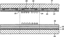
Be provided with transparent public X electrode 22 and transparent independent Y electrode 23 below glass prebasal plate 21, X bus electrode 24 and Y bus electrode 25 have superposeed respectively on electrode 21 and 22.On above-mentioned electrode 22,23,24,25, one deck dielectric layer 26 and protective seam 27 are provided, for example magnesium oxide (MgO).Be arranged on address A electrode 29 on the glass metacoxal plate 28 perpendicular to the public X electrode 22 and the independent Y electrode 23 that are arranged on the glass prebasal plate 21.Described address A electrode 29 is covered by one deck dielectric layer 30, and is provided with the partition wall 31 that parallels with address A electrode 29 on electrode 29.Fluorophor 32 is coated on partition wall 31 and the address A electrode 29.
Fig. 2 cut-open view of direction shown in the arrow A that is plasma display panel in Fig. 1.Address A electrode 29 is placed in the centre of two partition walls.Between glass prebasal plate 21 and glass metacoxal plate 38, filled the discharge gas such as neon and xenon in the formed space 33.
Fig. 3 cut-open view of direction shown in the arrow B that is plasma display panel in Fig. 1.The border with dashed lines of each luminescence unit represents that public X electrode 22 and independent Y electrode 23 are staggered.In the plasma display panel of AC type, the charged particle that is arranged near the dielectric layer public X electrode 22 and the independent Y electrode 23 is divided into positive charged particles and negative charge particle, and they have formed an electric field, thereby can discharge by this electric field.
Fig. 4 shows electrode and the circuit that is connected with the electrode of plasma display panel shown in Figure 1.Public X electrode 22 is connected with one or more lead-out terminals of X electrode drive circuit 35, and this circuit is delivered to public X electrode 22 with the driving pulse that is produced.Each independent Y electrode 23 is connected with the lead-out terminal of Y electrode drive circuit 36 respectively.Each address A electrode 29 is connected with the lead-out terminal of A electrode drive circuit 37 respectively.
Fig. 5 shows first drive system of first kind of embodiment of the present invention.Fig. 5 A is provided with time sequential chart of field in one according to the present invention.In the figure, one of Reference numeral 1 expression, abscissa express time wherein, ordinate is represented the delegation of luminescence unit.One is divided into 8 times, that is 2 to the 8th fields 9, the field first time.Set gradually charged particle balanced cycle 2A-9A, address cycle 2B-9B in the field each time, continuing cycle 2C-9C.Marked out the discharge time to each time, display gray scale then depends on the total degree of discharge.Order of presentation with time field of predetermined discharge number of times can be arbitrarily, but in this embodiment, is to arrange time field according to the ascending order of discharge time.
Fig. 5 A-5E shows the waveform that is respectively the pulse that public X electrode, address A electrode, the first and second independent Y electrodes provided.Among the figure, pulse waveform 10 is a part of drive pulse waveform that provided for public X electrode 22 in, pulse waveform 11 is a part of drive pulse waveform that provided for one of them ground also location A electrode 29, and a part of drive pulse waveform that is provided such as the first and second independent Y electrodes 23 is provided pulse waveform the 12, the 13rd.
The pulse waveform 10 that field interval is provided for public X electrode 22 in the first time comprises the adjustment pulse 40 and the lasting pulse 41 that is arranged in lasting cycle 2C that are lasted till address cycle 2B by the balanced cycle 2A of charged particle always.In this embodiment, the voltage of adjusting pulse 40 is lower than the voltage that continues pulse 41.The pulse waveform 11 that is applied to an address A electrode 29 comprises an address pulse 42 among the address cycle 2B, and this address pulse 42 is corresponding to the radiative luminescence unit of needs.If do not need luminous luminescence unit, just do not produce above-mentioned address pulse 42.In other words, with address pulse 42 deliver to need be more luminous luminescence unit, do not need luminous luminous glaze unit that address pulse 42 then is not provided for other.Deliver to first electrode of independent Y electrode 23 and the pulse waveform 12,13 of adjacent second electrode and be included in discharge particle equalizing pulse 43A, the 43B... that produces among the balanced cycle 2A of charged particle of the field first time, the scanning impulse 44A, the 44B... that in address cycle 2B, produce, and the lasting pulse 45A, the 45B... that in continuing cycle 2C, produce and thin horizontal blanking impulse 46A, 46B....In the present embodiment, the voltage of scanning impulse 44A, 44B... is lower than the voltage that continues pulse 45A, 45B....Thin horizontal blanking impulse 46A, 46B... are sent to identical electrode with equalizing pulse 43A, 43B....In addition, preferably the pulse width of thin horizontal blanking impulse 46A, 46B... is chosen as 0.5 μ sec-2 μ sec.
Introduce the working method of plasma display panel below.In Fig. 5, discharge in all luminescence units is carried out between independent Y electrode 28 and independent X electrode 22 by equalizing pulse 43A, 43B... are provided to independent Y electrode, in the balanced cycle 2A of charged particle that is right after after providing power supply for display, the negative charge particle forms in the dielectric of contiguous independent Y electrode 23.Discharge by equalizing pulse 43A, 43B... only occurs once when beginning, and just no longer occurs subsequently.In other words, discharge only occurs once, just no longer occurs when being in abnomal condition in the space 33 of luminescence unit.In the 0.3 μ sec-2 μ sec after equalizing pulse 43A, 43B... rising edge occurring, will adjust pulse 40 and deliver to public X electrode 22.Near formation negative charge particle public X electrode 22, and near address A electrode 29 the formation positive charged particles.
Why set the rising edge of equalizing pulse 43A, 43B... and adjust time relationship between the rising edge of pulse 40 according to above-mentioned requirements, be because if the time interval between the forward position of pulse 43A, 43B... and pulse 40 is oversize, will make too much negative charge particle accumulate near the independent Y electrode 23 public X electrodes 22; If the above-mentioned time interval is too short, positive charged particles can not accumulate on the address A electrode 22 the negative charge particle yet with regard to not accumulating in independent Y electrode 23.
It is that the negative charge particle is attracted to public X electrode 22 that the fundamental purpose of adjusting pulse 40 is provided, and forms positive charged particles on address A electrode 29.Another purpose is the discharge that helps when advancing the discharge of cloth address between address A electrode 29 and the independent Y electrode 23 between public X electrode 22 and the independent Y electrode 23.
When article one line of simultaneously scanning impulse 44A being delivered to independent Y electrode 23, address pulse 42 is delivered to address A electrode 29, thereby when making positive charged particles accumulate on the independent Y electrode 23, that luminescence unit that is positioned on the point of crossing of an article one line of independent Y electrode 23 and an address A electrode 22 carries out the address discharge.On the other hand, when the address pulse 42 corresponding to scanning impulse 44B... is not sent to the second line of independent Y electrode 23, thereby make when not having charged particle to assemble on the independent Y electrode 23, discharge just can not occur.Address pulse 42 is sent to address A electrode 29, it is corresponding to the luminous luminescence unit of needs, select all luminescence units on the point of crossing of all address A electrodes 29, and scanning impulse 44A or 44B... delivered to independent Y electrode 23, thereby between address A electrode 29 and independent Y electrode 23, discharge.
Subsequently, in lasting cycle 2C, discharge between the public X electrode 22 of such luminescence unit and independent Y electrode 23 by continuing pulse 41,45A, 45B..., this luminescence unit makes positive charged particles accumulate in independent Y electrode 23 1 sides by the discharge of being carried out among the address cycle 2B.After this,, between independent Y electrode 23 and public X electrode 22, discharge by thin horizontal blanking impulse 46A, 46B... are delivered to independent Y electrode 23, the charged particle in the blanking luminescence unit, thereby produce in the blanking luminescence unit be used for luminous charged particle.The pulse width of thin horizontal blanking impulse 46A, 46B... is slightly greater than the discharge period, because of than making the negative charge particle accumulate near the independent Y electrode 23 the dielectric layer.In the luminescence unit that does not occur discharging,, therefore can not carry out the blanking discharge owing to there is not charged particle.Like this, formed negative charge particle will remain unchanged near independent Y electrode 23.
Under these circumstances, equalizing pulse 43A, 43B... are delivered to independent Y electrode 23 discharge just can not occur,, be not enough to produce the electric field of discharge thereby have to form because the negative charge particle in the luminescence unit has been offset the voltage of equalizing pulse 43A, 43B....After this, even in all time fields, provide equalizing pulse, can not produce discharge yet.Like this, in first time field that after energized, is right after, can not produce discharge, thereby in black display, can not produce light emission.
In addition, for the linearity by the lasting determined display gray scale of pulse number, once discharge is littler than twice discharge influence.According to the present invention, the equilibrium of charged particle is to realize by discharging in the luminescence unit that continues into thousand discharge, and is therefore very little to the influence of the linearity of display gray scale.
Carry out identical driving operation in during 3 to the 8th fields 9, the field second time, thereby finish one screen.
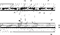
Fig. 6-the 10th, the cut-open view of plasma display panel, show after energized the first time field to for the second time up to equalizing pulse being provided and adjusting pulse, charged particle carries out the situation of continuous discharge in luminescence unit.In these figure, reference number 60 expression positive charged particles, reference number 61 expression negative charge particles.In addition, show the charged particle distribution situation of the luminescence unit that is arranged in Fig. 6-7 middle body.
Fig. 6 is the cut-open view of the Plasma Display utmost point, the figure shows to be right after in energized and after providing balanced and adjusting pulse the distribution situation of charged particle in luminescence unit.The figure shows at first after energized, then equalizing pulse 43A, 43B... are delivered to independent Y electrode 23, provide at last when adjusting pulse 40, for the first time the distribution situation of the charged particle in.In all luminescence units, by equalizing pulse 43A, 43B... being offered independent Y electrode 23, between public X electrode 22 and independent Y electrode 23, produce discharge, negative charge particle 61 accumulates near independent Y electrode 23 and the public X electrode 22 the dielectric layer, and positive charged particles 60 accumulates on the side of address A electrode 29.
Fig. 7 is the cut-open view of plasma display panel, shows the distribution situation of charged particle in luminescence unit after carrying out the address discharge.In Fig. 7, show and address pulse 42 is being delivered to address A electrode 29, and the charged particle distribution situation after discharge in the generation address between address A electrode 29 and independent Y electrode 23.Positive charged particles 60 accumulates near the independent Y electrode 23 the dielectric layer, because the voltage on the independent Y electrode 23 is lower than the voltage on address A electrode 29 and the public X electrode 22.Fig. 7 shows the distribution situation of charged particle.By positive charged particles 60 and offer the lasting pulse 45A of independent Y electrode 23, first pulse of 45B..., between independent Y electrode 23 and public X electrode 22, produce discharge.This is a kind of continuous discharge.At this moment, by by continuing the discharge that pulse 45A, 45B... produce, negative charge particle 61 is accumulated in around the independent Y electrode 23, positive charged particles 62 accumulates in public X electrode 22.Like this, by continuing first pulse of pulse, between independent Y electrode 23 and public X electrode 22, produce continuous discharge.In lasting cycle 2C, above-mentioned discharge is repeatedly carried out.
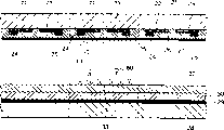
Fig. 8 is the cut-open view of the Plasma Display utmost point, there is shown the charged particle distribution situation in the luminescence unit after thin horizontal blanking impulse is provided.Fig. 8 shows in that last lasting pulse 41 is offered public X electrode 22, and thin horizontal blanking impulse 46a is provided then, the charged particle distribution situation after the 46b....
In the end after the discharge of lasting pulse 41 generations, the distribution situation of charged particle is identical with distribution situation shown in Figure 7.
The pulse width of thin horizontal blanking impulse 46A, 46B... is longer than the discharge period, so the negative charge particle 61 of rapid movement accumulates on the dielectric layer of contiguous independent Y electrode 23.Like this, just realized the separation of charged particle.Moving slowly in the space, positive charged particles is suspended in the luminescence unit.The negative charge particle is done of short duration suspension in discharge space.
Fig. 9 is the cut-open view of plasma display panel, and showing is providing the charged particle distribution situation in the luminescence unit after the equalizing pulse in the field for the second time.Fig. 9 shows after providing equalizing pulse 43A, 43B... in the field second time, the distribution situation of charged particle.The voltage of equalizing pulse 43A, 43B... is offset by negative charge, does not reach sparking voltage, thereby can not produce discharge.The voltage of independent Y electrode 23 is higher than the voltage of other electrodes, so negative charge attracted to independent Y electrode 23.
Figure 10 is the cut-open view of plasma display panel, shows after providing the adjustment pulse in the field second time charged particle distribution situation in the luminescence unit.
This illustrates and offers public X electrode 22 charged particle distribution situation afterwards with adjusting pulse 40.The negative charge particle accumulates on the dielectric layer of contiguous public X electrode 22, and positive charged particles accumulates on the address A electrode 29.Like this, do not need to produce discharge, just can realize and an identical driving for the first time by equalizing pulse 43A, 43B....Under these circumstances, the voltage of equalizing pulse 43A, 43B... is reduced by the negative charge particle on the independent Y electrode 23, therefore can not produce discharge between independent Y electrode 23 and public X electrode 22.
Can under the situation that field is not each time write fully discharge and thin horizontal blanking discharge, realize the driving of article on plasma body display board.Consequently for the black brightness blanking that shows unnecessary light emission, thereby improved contrast.
Below second kind of embodiment of the present invention described.Figure 11 shows the second kind of drive system of second kind of embodiment according to the present invention.Figure 11 A is a sequential chart, has represented to be provided with in one according to the present invention time situation of field.As Fig. 5, the figure illustrates Jiang Yichang and be divided into the several times field.Wherein abscissa is the time, and ordinate is the row of luminescence unit.
Figure 11 B-11E shows the pulse waveform that offers public X electrode, address A electrode and the first and second independent Y electrodes respectively.
Pulse waveform 70 is the parts that offer the drive waveforms of public X electrode 22 in.Pulse waveform 71 provides the part to the drive waveforms of an address A electrode 29.Pulse waveform 72 and 73 provides to the part such as the drive waveforms of the first and second independent Y electrodes 23.
Pulse waveform 70 offers public X electrode 22 in first time field, it comprises the adjustment pulse 40 that is extended to address cycle 2B by the balanced cycle 2A of charged particle, and lasting pulse in continuing cycle 2C 41 and thin horizontal blanking impulse 74.The pulse waveform 71 that offers address A electrode 29 comprises the address pulse 42 among the address cycle 2B, and it is corresponding to the luminous luminescence unit of needs.When not needing luminous luminescence unit, just do not provide above-mentioned address pulse 42.Offer first electrode of independent Y electrode 23 and independent Y electrode 23 the pulse waveform of second electrode comprise: charged particle equalizing pulse 43A, the 43B... of charged particle in the balanced cycle for the first time, and scanning impulse 44A, 44B... among the address cycle 2B, continue lasting pulse 45A, 45B... and first thin horizontal blanking impulse 75A, the 75B... among the cycle 2C.
In these cases, the pulse width of first thin horizontal blanking impulse 75A, 75B... is equal to or less than the pulse width of the second thin horizontal blanking impulse 74.As shown in figure 11, the number of thin horizontal blanking impulse is an even number, that is first and second thin horizontal blanking impulse 75A, 75B... and 74, first thin horizontal blanking impulse 75A, 75B... and the equalizing pulse 43a as last blanking pulse, 43b is sent to identical electrode, that is independent Y electrode 23 shown in Figure 11.The second thin horizontal blanking impulse 74 is sent to another electrode, that is public X electrode 22.
In this embodiment, last lasting pulse is sent to independent Y electrode 23.The first thin horizontal blanking impulse 75a is being provided, and after the 75b, the distribution situation of the distribution situation of charged particle and first embodiment shown in Figure 8 is basic identical.Charged particle distribution situation in the 3-9 of other times field also is identical.In addition, the blanking of charged particle and polarization are undertaken by above-mentioned thin horizontal blanking impulse, so these blanking pulses are called as the polarization pulse group.In this embodiment, by adopting first and second thin horizontal blanking impulse 75A, the 75B..., 74, can carry out blanking and polarization effectively, keep the discharge time in the discharge cycle of address constant.
Below the third embodiment of the present invention is described.Figure 12 shows the third drive system of the third embodiment according to the present invention.Figure 12 A is a sequential chart, shows according to the present invention time situation of field is set in one.As Fig. 5, this accompanying drawing has shown that Jiang Yichang is divided into the situation of several times field.Wherein abscissa is the time, and ordinate is the row of luminescence unit.
Figure 12 B-12E shows the pulse waveform that offers public X electrode, address A electrode and the first and second independent Y electrodes respectively.
Pulse waveform 80 is the parts that offer the drive waveforms of public X electrode 22 in the first time in the field.Pulse waveform 81 provides the part to the drive waveforms of an address A electrode 29.Pulse waveform 82 and 83 provides to the part such as the drive waveforms of the first and second independent Y electrodes 23.
Pulse waveform 80 offers public X electrode 22 in first time field, it comprises the adjustment pulse 40 that is extended to address cycle 2B by the balanced cycle 2A of charged particle, and the lasting pulse 41 and the second thin horizontal blanking impulse 84 in continuing cycle 2C.The pulse waveform 81 that offers address A electrode 29 comprises the address pulse 42 among the address cycle 2B, and it is corresponding to the luminous luminescence unit of needs.When not needing luminous luminescence unit, just do not provide above-mentioned address pulse 42.Offering first electrode of independent Y electrode 23 and the second electrode pulse waveform 82,83 of independent Y electrode 23 comprises: charged particle equalizing pulse 43A, 43B... among the cycle 2A of the charged particle of field equilibrium for the first time, scanning impulse 44A, 44B... among the address cycle 2B continue lasting pulse 45A, 45B..., the 3rd thin horizontal blanking impulse 85A, 85B... and first thin horizontal blanking impulse 86A, the 86B... among the cycle 2C.
In these cases, the pulse width of the second thin horizontal blanking impulse 84 is equal to or less than the pulse width of the 3rd thin horizontal blanking impulse 85A, 85B....
The pulse width of first thin horizontal blanking impulse 86A, 86B... is equal to or less than the pulse width of the second thin horizontal blanking impulse 84.
As shown in figure 12, if the number of thin horizontal blanking impulse is an odd number, that is first to the 3rd thin horizontal blanking impulse, first thin horizontal blanking impulse 86A, the 86B... and equalizing pulse 43A, 43B... as the blanking pulse that provides at last are sent to identical electrode, that is independent Y electrode 23 shown in Figure 12.The 3rd thin horizontal blanking impulse 85 as the thin horizontal blanking impulse that at first provides is sent to and the identical electrode of electrode that provides first thin horizontal blanking impulse 86A, the 86B..., that is independent Y electrode 23.Therefore, last lasting pulse is sent to public X electrode 22.The distribution situation of charged particle distribution situation after first thin horizontal blanking impulse 86A, the 86B... is provided and first kind of embodiment of the present invention shown in Figure 8 is basic identical.Discharged condition in all the other times 3-9 is identical.In this embodiment, by adopting first, second, third thin horizontal blanking impulse 86A, 86B, 84,85A, 85B, can more effectively carry out blanking and polarization, it is constant that the discharge in the interdischarge interval of address can keep.According to the experiment that the present inventor carried out, for thin horizontal blanking, adopting many thin horizontal blanking impulses to 3 is effectively, and adopts the thin horizontal blanking impulse more than 4 just so ineffective.
Below the 4th kind of embodiment of the present invention described.Figure 13 shows the 4th kind of drive system of the 4th kind of embodiment according to the present invention.Figure 13 A is a sequential chart, shows according to the present invention time situation of field is set in one.As Fig. 5, this accompanying drawing has shown that Jiang Yichang is divided into the situation of several times field.Wherein abscissa is the time, and ordinate is the row of luminescence unit.
Figure 13 B-13E shows the pulse waveform that offers public X electrode, address A electrode and the first and second independent Y electrodes respectively.
Pulse waveform 90 is the parts that offer the drive waveforms of public X electrode 22 in the first time in the field.Pulse waveform 91 provides the part to the drive waveforms of an address A electrode 29.Pulse waveform 92 and 93 provides to the part such as the drive waveforms of the first and second independent Y electrodes 23.
Pulse waveform 90 offers public X electrode 22 in first time field, it comprises the adjustment pulse 94 that is extended to address cycle 2B by the balanced cycle 2A of charged particle, and the lasting pulse 41 among the lasting cycle 2C.
The voltage of adjustment pulse 94 is identical with the voltage of lasting pulse 41, thereby makes driving circuit obtain simplifying, because can adopt identical power supply.
The pulse waveform 91 that offers an address A electrode 29 comprises the address pulse 42 among the address cycle 2B, and it is corresponding to the luminous luminescence unit of needs.When not needing luminous luminescence unit, just do not provide above-mentioned address pulse.The pulse waveform 92,93 that offers second electrode of first electrode of independent Y electrode 23 and adjacent independent Y electrode 23 comprises: charged particle equalizing pulse 43A, the 43B... among the balanced cycle 2A of charged particle for the first time, scanning impulse 44A, 44B... among the address cycle 2B continue lasting pulse 45A, 45B... and thin horizontal blanking impulse 46A, 46B... among the cycle 2C.The charged particle distribution situation of charged particle distribution situation after thin horizontal blanking impulse 46A, 46B... are provided and first kind of embodiment of the present invention shown in Figure 8 is essentially identical.Charged particle distribution situation in remaining time 3-9 is identical.In this embodiment, the voltage of adjustment pulse 94 that offers public X electrode 22 is identical with the voltage of lasting pulse, thereby has simplified the circuit structure of driving circuit.
Below the 5th kind of embodiment of the present invention described.Figure 14 shows the 5th kind of drive system of the 5th kind of embodiment of the present invention.Figure 14 A is a sequential chart, shows according to the present invention time situation of field is set in one.As Fig. 5, this accompanying drawing has shown that Jiang Yichang is divided into the situation of several times field.Wherein abscissa is the time, and ordinate is the row of luminescence unit.Figure 14 B-14E shows the pulse waveform that offers public X electrode, address A electrode and the first and second independent Y electrodes respectively.
The pulse waveform 100 that offers public X electrode 22 in first time field comprises the adjustment pulse 94 that is extended to address cycle 2B by the balanced cycle 2A of charged particle, and the lasting pulse 41 among the lasting cycle 2C.As the 4th kind of embodiment shown in Figure 13, the voltage of adjusting pulse 94 is identical with the voltage of lasting pulse 41, thereby has simplified driving circuit, because can adopt identical power supply.The pulse waveform 101 that offers an address A electrode 29 comprises the address pulse 42 among the address cycle 2B, and it is corresponding to the luminous luminescence unit of needs.When not needing luminous luminescence unit, just do not provide above-mentioned address pulse 42.The pulse waveform 102,103 that offers second electrode of first electrode of independent Y electrode 23 and adjacent independent Y electrode 23 comprises: charged particle equalizing pulse 43A, the 43B... among the balanced cycle 2A of charged particle for the first time, scanning impulse 104A, 104B... among the address cycle 2B continue lasting pulse 45A, 45B... and thin horizontal blanking impulse 46A, 46B... among the cycle 2C.Independent Y electrode 23 is identical with the voltage of lasting pulse 45A, 45B... at the voltage of address cycle 2C, thereby has simplified driving circuit, because can adopt identical power supply.The charged particle distribution situation of charged particle distribution situation after thin horizontal blanking impulse 46A, 46B... are provided and first kind of embodiment of the present invention shown in Figure 8 is essentially identical.Charged particle distribution situation in remaining time 3-9 is identical.
Below the 6th kind of embodiment of the present invention described.Figure 15 shows the 6th kind of drive system of the 6th kind of embodiment of the present invention.Figure 15 A is a sequential chart, shows according to the present invention time situation of field is set in one.As Fig. 5, this accompanying drawing has shown that Jiang Yichang is divided into the situation of several times field.Wherein abscissa is the time, and ordinate is the row of luminescence unit.Figure 15 B-15E shows the pulse waveform that offers public X electrode, address A electrode and the first and second independent Y electrodes respectively.
Pulse waveform 110 is the parts that offer the drive waveforms of public X electrode 22 in the first time in the field.Pulse waveform 111 provides the part to the drive waveforms of an address A electrode 29.Pulse waveform 112 and 113 provides to the part such as the drive waveforms of the first and second independent Y electrodes 23.
The pulse waveform 100 that offers public X electrode 22 in first time field comprises by first among the balanced cycle 2A of charged particle adjusts pulse 114, and second among the address cycle 2B adjusts pulse 115, and the lasting pulse 41 among the lasting cycle 2C.The adjustment pulse that is provided to public X electrode 22 is divided into first among the balanced cycle 2a of charged particle and adjusts second among pulse 114 and the address cycle 2b and adjust pulse 115.The pulse waveform 111 that offers an address A electrode 29 comprises the address pulse 42 among the address cycle 2B, its corresponding with need luminous luminescence unit.When not needing luminous luminescence unit, just do not provide above-mentioned address pulse 42.The pulse waveform 112,113 that offers second electrode of first electrode of independent Y electrode 23 and adjacent independent Y electrode 23 comprises: charged particle equalizing pulse 43A, the 43B... among the balanced cycle 2A of charged particle for the first time, scanning impulse 114A, 114B... among the address cycle 2B continue lasting pulse 45A, 45B... and thin horizontal blanking impulse 46A, 46B... among the cycle 2C.The charged particle distribution situation of charged particle distribution situation after thin horizontal blanking impulse 46A, 46B... are provided and first kind of embodiment of the present invention shown in Figure 8 is essentially identical.Charged particle distribution situation in remaining time 3-9 is identical.In Figure 15, discharge thereby prevented from owing to error to produce between public X electrode 22 and independent Y electrode slightly early than the back edge of equalizing pulse 43A in the first back edge of adjusting pulse.In addition, the forward position of the second adjustment pulse and the forward position of scanning impulse 115 occur simultaneously, thereby have prevented the generation discharge between public X electrode 22 and independent Y electrode 23 owing to slip up.
Deliver to the first adjustment pulse 114 of public X electrode 22 and can adopt identical voltage with lasting pulse 41.
Below the 7th kind of embodiment of the present invention described.Figure 16 shows the 7th kind of drive system of the 7th kind of embodiment according to the present invention.Figure 16 A is a sequential chart, shows according to the present invention time situation of field is set in one.As Fig. 5, this accompanying drawing has shown that Jiang Yichang is divided into the situation of several times field.Wherein abscissa is the time, and ordinate is the row of luminescence unit.
Figure 16 B-16E shows the pulse waveform that offers public X electrode, address A electrode and the first and second independent Y electrodes respectively.
Pulse waveform 130 is the parts that offer the drive waveforms of public X electrode 22 in the first time in the field.Pulse waveform 131 provides the part to the drive waveforms of an address A electrode 29.Pulse waveform 132 and 133 provides to the part such as the drive waveforms of the first and second independent Y electrodes 23.
The pulse waveform 131 that offers public X electrode 22 in first time field comprises that first of the balanced cycle 2A of charged particle adjusts pulse 134, continues second among the cycle 2B and adjusts pulse 135, and the lasting pulse 41 among the lasting cycle 2C.Address pulse 42 among the address cycle 2B that the pulse waveform 131 that offers an address A electrode 29 comprises for the first time, it is corresponding to the luminous luminescence unit of needs.When not needing luminous luminescence unit, just do not provide above-mentioned address pulse 42.The pulse waveform 132,133 that offers second electrode of first electrode of independent Y electrode 23 and adjacent with it independent Y electrode 23 comprises: charged particle equalizing pulse 136A, the 136B... among the balanced cycle 2A of charged particle for the first time, scanning impulse 137A, 137B... among the address cycle 2B continue lasting pulse 45A, 45B... and thin horizontal blanking impulse 46A, 46B... among the cycle 2C.
According to present embodiment, the back edge of equalizing pulse 136A, 136B... is zero in less than the time of 1 μ s, and this point is different from aforesaid embodiment.Adjust pulse 135 and scanning impulse 137A, 137B... for second, can provide and lasting pulse 41, voltage that 45A, 45B... are identical.The charged particle distribution situation of charged particle distribution situation after thin horizontal blanking impulse 46A, 46B... are provided and first kind of embodiment of the present invention shown in Figure 8 is essentially identical.Charged particle distribution situation in remaining time 3-9 is identical.
In this embodiment, as shown in figure 16, first adjusts the whereabouts of the whereabouts at pulse 139 edges early than the equalizing pulse edge, thereby has prevented the generation discharge between public X electrode 22 and independent Y electrode owing to slip up.
Below the 8th kind of embodiment of the present invention described.Figure 17 shows the 8th kind of drive system of the 8th kind of embodiment according to the present invention.Figure 17 A is a sequential chart, shows according to the present invention time situation of field is set in one.As Fig. 5, this accompanying drawing has shown that Jiang Yichang is divided into the situation of several times field.Wherein abscissa is the time, and ordinate is the row of luminescence unit.Figure 17 B-17E shows the pulse waveform that offers public X electrode, address A electrode and the first and second independent Y electrodes respectively.
The pulse waveform 141 that offers public X electrode 22 in first time field comprises the adjustment pulse 144 among the balanced cycle 2A of charged particle, second adjusts pulse 145 in address cycle 2B, and the lasting pulse 41 among the lasting cycle 2C.
According to present embodiment, first voltage of adjusting pulse 144 is higher than the voltage that continues pulse 41.The pulse waveform 141 that offers an address A electrode 29 comprises the address pulse 42 among the address cycle 2B of first another arena, and it is corresponding to the luminous luminescence unit of needs.When not needing luminous luminescence unit, just do not provide above-mentioned address pulse 42.The pulse waveform 142,143 that offers second electrode of first electrode of independent Y electrode 23 and adjacent with it independent Y electrode 23 comprises: charged particle equalizing pulse 136A, the 136B... among the balanced cycle 2A of charged particle for the first time, scanning impulse 137A, 137B... among the address cycle 2B continue lasting pulse 45A, 45B... and thin horizontal blanking impulse 46A, 46B... among the cycle 2C.
The voltage of the second adjustment pulse 144 and the voltage of scanning impulse 137A, 137B... can be identical with the voltage of lasting pulse 41,45A, 45B....The charged particle distribution situation of charged particle distribution situation after thin horizontal blanking impulse 46A, 46B... are provided and first kind of embodiment of the present invention shown in Figure 8 is essentially identical.Charged particle distribution situation in remaining time 3-9 is identical.
According to present embodiment, first voltage of adjusting pulse 144 is higher than the voltage that continues pulse 41.Adopt higher voltage by adjusting pulse to first, just can collect many negative charge particles, consequently many positive charged particles are collected into address A electrode 29 1 sides, thereby can very easily carry out the address discharge.
Below the 9th kind of embodiment of the present invention described.Figure 18 shows the 9th kind of drive system of the 9th kind of embodiment of the present invention.Figure 18 A is a sequential chart, shows according to the present invention time situation of field is set in one.As Fig. 5, this accompanying drawing has shown that Jiang Yichang is divided into the situation of several times field.Wherein abscissa is the time, and ordinate is the row of luminescence unit.Figure 18 B-18E shows the pulse waveform that offers public X electrode, address A electrode and the first and second independent Y electrodes respectively.
The pulse waveform 151 that offers public X electrode 22 in for the first time comprises the equalizing pulse 153 among the balanced cycle 2A of charged particle, second adjusts pulse 154 in address cycle 2B, and lasting pulse among the lasting cycle 2C 41 and thin horizontal blanking impulse 155.
According to present embodiment, provide unique thin horizontal blanking impulse 155.As at the 5th kind of embodiment, equalizing pulse 153 is offered that electrode of accepting thin horizontal blanking impulse 155.When the number of thin horizontal blanking impulse as second kind and the third embodiment is 2 or 3 (referring to Figure 11 and Figure 12), this equalizing pulse is offered that electrode that last thin horizontal blanking impulse offers.
The pulse waveform 151 that offers an address A electrode 29 comprises the address pulse 42 among the address cycle 2B of first subdomain, and it is corresponding to the luminous luminescence unit of needs.When not needing luminous luminescence unit, just do not provide above-mentioned address pulse 42.The pulse waveform 152,153 that offers second electrode of first electrode of independent Y electrode 23 and adjacent with it independent Y electrode 23 comprises: the first equalizing pulse 156A, the 156B... among the balanced cycle 2A of charged particle for the first time, scanning impulse 137A, 137B... among the address cycle 2B continue lasting pulse 45A, 45B... among the cycle 2C.
In this embodiment, provide first to adjust pulse 156A, 156B... in the 0.3-2 μ s time durations after the forward position of equalizing pulse 153.
As the 5th kind of embodiment (referring to Figure 14), the voltage of the second adjustment pulse 144 and the voltage of scanning impulse 137A, 137B... can be identical with the voltage of lasting pulse 41,45A, 45B....The charged particle distribution situation of charged particle distribution situation after thin horizontal blanking impulse 46A, 46B... are provided and first kind of embodiment of the present invention shown in Figure 8 is essentially identical.Charged particle distribution situation in remaining time 3-9 is identical.
According to this embodiment, the first adjustment pulse 43A, 43B... are similar to equalizing pulse 43A, 43B... shown in Figure 15, but according to the present invention, an equalizing pulse at first occurs in the balanced cycle at charged particle.Adjust in the forward position of equalizing pulse 153 and first and between the forward position of pulse 156A, 156B... the reason in the time interval of 0.3-2 μ s is set and explains in front.
Figure 19-the 23rd, the cut-open view of the plasma display panel of the 9th kind of embodiment according to the present invention, they show the second time field of the field first time till equalizing pulse is provided and adjusts pulse after energized, the situation that the charged particle in the luminescence unit discharges for the light emission.In these figure, Reference numeral 60 is used to represent positive charged particles, Reference numeral 61 expression negative charge particles.In addition, there is shown the charged particle distribution situation of the luminescence unit that is positioned at Figure 19-23 middle part.
Figure 19 is the cut-open view of a plasma display panel, show to be right after in energized, and provide subsequently equalizing pulse and the protection pulse after the time the charged particle distribution situation.The figure shows in energized at first, then equalizing pulse 153 offered public X electrode 22, provide first to adjust after pulse 156A, the 156B... at last, for the first time in the distribution situation of charged particle.By equalizing pulse 153 being offered the independent Y electrode 23 in all luminescence units, between public X electrode 22 and independent Y electrode 23, produce discharge, negative charge particle 61 accumulate in independent Y electrode 23 and public X electrode 22 near, and positive charged particles 60 accumulates in address A electrode 29 1 sides.
Figure 20 is the cut-open view of the plasma display panel of the 9th kind of embodiment of the present invention, shows after carrying out address discharge the charged particle distribution situation in the luminescence unit.Figure 20 shows address pulse 42 is offered address A electrode 29, the situation after discharging between address A electrode 29 and the independent Y electrode 23.Because the voltage of independent Y electrode 23 is lower than the voltage of address A electrode 29 and public X electrode 22, so positive charged particles 60 accumulates near the independent Y electrode 23 the dielectric layer.Negative charge particle 61 accumulates in a side of other electrodes.
Figure 20 shows the distribution situation of charged particle.Offer independent Y electrode 23 by first pulse, between independent Y electrode 23 and public X electrode 22, produce continuous discharge positive charged particles 60 and lasting pulse 45A, 45B....Continuous discharge that Here it is.
Figure 21 is the cut-open view of the Plasma Display utmost point, shows the charged particle distribution situation after thin horizontal blanking impulse is provided.In Figure 21, show last lasting pulse 45A, 45B... are offered after the independent Y electrode 23, the charged particle distribution situation when then thin horizontal blanking impulse 155 being offered public X electrode 22.
The pulse width of thin horizontal blanking impulse 155 is longer than the discharge period, thereby makes the negative charge particle 61 that moves rapidly accumulate near the public X electrode 22 the dielectric layer, and moving slowly in the space, positive charged particles 60 then is suspended in the luminescence unit.The negative charge particle only suspends in discharge space the short time.
Figure 22 is the cut-open view of the plasma display panel of the 9th kind of embodiment of the present invention, and showing is providing equalizing pulse charged particle distribution situation afterwards in the field for the second time.
In Figure 22, showing is providing equalizing pulse 153 discharged condition afterwards in the field for the second time.The voltage of equalizing pulse 153 is offset by negative charge particle 61, does not reach sparking voltage, therefore any discharge can not occur.
Figure 23 is the cut-open view of plasma display panel, and showing is providing the adjustment pulse distribution situation of charged particle in luminescence unit afterwards in the field for the second time.
In the figure, show and adjusting pulse 156A, the 156B... charged particle distribution situation after offering independent Y electrode 23 first.Negative charge particle 61 accumulates near public X electrode 22 and the independent Y electrode 23 the dielectric layer, and positive charged particles 60 accumulates on the address A electrode 29.Like this, need not produce discharge, just can realize and an identical driving for the first time by equalizing pulse 153.
Below the of the present invention ten kind of embodiment described.Figure 24 shows the tenth kind of drive system of the tenth kind of embodiment according to the present invention.Figure 24 A is a sequential chart, shows according to the present invention time situation of field is set in one.As Figure 18, the figure illustrates the situation that Jiang Yichang is divided into the several times field.Wherein abscissa is the time, and ordinate is the row of luminescence unit.Figure 24 B-24E shows the pulse waveform that offers public X electrode, address A electrode and the first and second independent Y electrodes respectively.
The pulse waveform 160 that offers public X electrode 22 in first time field comprises the equalizing pulse 163 among the balanced cycle 2A of charged particle, equalizing pulse 164 continuities from balanced cycle 2A of charged particle and address cycle 2B, second adjusts pulse 165, and lasting pulse among the lasting cycle 2C 41 and thin horizontal blanking impulse 155.
According to present embodiment, only provide a thin horizontal blanking impulse.As first kind of embodiment, equalizing pulse 164 is offered that electrode that thin horizontal blanking impulse 155 is offered.If the number of thin horizontal blanking impulse is two or three as second embodiment or the 3rd embodiment (referring to Figure 11 and Figure 12), then equalizing pulse is offered that electrode that last thin horizontal blanking impulse offers.Address pulse 42 among the address cycle 2B that the pulse waveform 161 that offers an address A electrode 29 comprises for the first time, it is corresponding to the luminous luminescence unit of needs.When not needing luminous luminescence unit, just do not provide above-mentioned address pulse 42.The pulse waveform 162,163 that offers second electrode of first electrode of independent Y electrode 23 and adjacent independent Y electrode 23 comprises: first among the balanced cycle 2A of charged particle adjusts pulse 156A, 156B... for the first time, scanning impulse 137A, 137B... among the address cycle 2B continue lasting pulse 45A, 45B... among the cycle 2C.In this embodiment, provide first to adjust pulse 156A, 156B... in the 0.3-2 μ s time durations after the forward position of equalizing pulse 153.As the 9th kind of embodiment (referring to Figure 18), the voltage of the second adjustment pulse 165 and the voltage of scanning impulse 137A, 137B... can be identical with the voltage of lasting pulse 41,45A, 45B....Situation among all the other times 3-9 is with the field is identical for the first time.
Charged particle distribution situation after thin horizontal blanking impulse 46A, 46B... are provided and situation shown in Figure 8 are basic identical, the figure shows the charged particle distribution situation of first kind of embodiment of the present invention.Charged particle distribution situation in all the other times 3-9 kind is identical.
According to present embodiment, the purpose that the voltage of equalizing pulse 164 is set to high voltage be with the negative charge particle collection in public X electrode one side, and positive charged particles as much as possible is collected on the independent Y electrode 29.In addition, second purpose of adjusting the voltage of pulse 165 being set in address cycle among the 2B is to prevent to produce between public X electrode 22 and independent Y electrode 23 wrong discharge.
Below the 11 kind of embodiment of the present invention described.Figure 25 shows the 11 kind of drive system of the 11 kind of embodiment according to the present invention.Figure 25 A is a sequential chart, shows according to the present invention time situation of field is set in one.As Fig. 5, this accompanying drawing has shown that Jiang Yichang is divided into the situation of several times field.Wherein abscissa is the time, and ordinate is the row of luminescence unit.Figure 25 B-25E shows the pulse waveform that offers public X electrode, address A electrode and the first and second independent Y electrodes respectively.
Pulse waveform 170 is the parts that offer the drive waveforms of public X electrode 22 in the first time in the field.Pulse waveform 171 provides the part to the drive waveforms of an address A electrode 29.Pulse waveform 172 and 173 provides to the part such as the drive waveforms of the first and second independent Y electrodes 23.
The pulse waveform 170 that offers public X electrode 22 in first time field comprises the adjustment pulse 40 that is extended to address cycle 2B by the balanced cycle 2A of charged particle, and the lasting pulse 41 among the lasting cycle 2C.The pulse waveform 171 that offers an address A electrode 29 comprises: voltage keeps pulse 174, chooses the voltage of this pulse, makes to be unlikely to cause discharge at scanning impulse 44A, 44B...; Address pulse 42 in the address cycle 2B of the first address cycle 2B, it is corresponding to Optical Transmit Unit and between address A electrode 29 and independent Y electrode 23.When not needing luminous luminescence unit, just do not provide address pulse 42.According to present embodiment, keep the voltage of pulse 174 and the voltage sum of address pulse 175 for the address required voltage of discharge equals voltage, thereby reduced the voltage of address pulse 175.When not needing luminous luminescence unit, just do not provide address pulse 175.The pulse waveform 172,173 that offers second electrode of first electrode of independent Y electrode 23 and adjacent independent Y electrode 23 comprises: equalizing pulse 43A, the 43B... among the balanced cycle 2A of charged particle for the first time, scanning impulse 44A, 44B... among the address cycle 2B continue lasting pulse 45A, 45B... among the cycle 2C.The voltage of adjusting pulse 40 and scanning impulse 44A, 44B... can be identical with the voltage of lasting pulse 41,45A, 45B....
Charged particle distribution situation after thin horizontal blanking impulse 46A, 46B... are provided and situation shown in Figure 8 are basic identical, the figure shows the charged particle distribution situation of first kind of embodiment of the present invention.Charged particle distribution situation in all the other times 3-9 kind is identical.
Below the 12 kind of embodiment of the present invention described.Figure 26 shows the 12 kind of drive system of the 12 kind of embodiment according to the present invention.Figure 26 A is a sequential chart, shows according to the present invention time situation of field is set in one.As Fig. 5, this accompanying drawing has shown that Jiang Yichang is divided into the situation of several times field.Wherein abscissa is the time, and ordinate is the row of luminescence unit.Figure 26 B-26E shows the pulse waveform that offers public X electrode, address A electrode and the first and second independent Y electrodes respectively.
Pulse waveform 180 is the parts that offer the drive waveforms of public X electrode 22 in the first time in the field.Pulse waveform 181 provides the part to the drive waveforms of an address A electrode 29.Pulse waveform 182 and 183 provides to the part such as the drive waveforms of the first and second independent Y electrodes 23.
The pulse waveform 180 that offers public X electrode 22 in first time field comprises the adjustment pulse 184 among the balanced cycle 2A of charged particle, and the lasting pulse 41 among the lasting cycle 2C.
The pulse waveform 171 that offers an address A electrode 29 is included in the address pulse 42 among the address cycle 2B of the first address cycle field, and it is corresponding to the luminous luminescence unit of needs.If do not need luminous luminescence unit, just do not provide address pulse 42.Offering first electrode of independent Y electrode 23 and the second electrode pulse waveform 182,183 of adjacent independent Y electrode 23 comprises: the first equalizing pulse 43A, the 43B... among the balanced cycle 2A of charged particle for the first time, scanning impulse 137A, 137B... among the address cycle 2B, lasting pulse 185A, 185B... among the address cycle 2B, and lasting pulse 45A, 45B... among the lasting cycle 2C and thin horizontal blanking impulse 46A, 46B....The voltage of adjusting pulse 184 can be identical with the voltage of lasting pulse 41.
Charged particle distribution situation after thin horizontal blanking impulse 46A, 46B... are provided and situation shown in Figure 8 are basic identical, the figure shows the charged particle distribution situation of first kind of embodiment of the present invention.Charged particle distribution situation in all the other times 3-9 is identical.According to present embodiment, the voltage of scanning impulse 185A, 185B... is negative voltage, and the voltage of address pulse 42 is positive voltage, so voltage difference becomes very big, thereby can guarantee to produce discharge.
Below the 13 kind of embodiment of the present invention described.Figure 27 shows the 13 kind of drive system of the 13 kind of embodiment according to the present invention.Figure 27 A is a sequential chart, shows according to the present invention time situation of field is set in one.As Figure 18, this accompanying drawing has shown that Jiang Yichang is divided into the situation of several times field.Wherein abscissa is the time, and ordinate is the row of luminescence unit.Figure 27 B-27E shows the pulse waveform that offers public X electrode, address A electrode and the first and second independent Y electrodes respectively.
The pulse waveform 190 that offers public X electrode 22 in the 8th time and after this field blank cycle 9D comprises among the balanced cycle 2A of charged particle and is extended to adjustment pulse 40 among the address cycle 2B by balanced cycle 2A, and the lasting pulse 41 among the lasting cycle 2G and write pulse 194 entirely.In this embodiment,, thereby can both produce discharge no matter whether carried out continuous discharge entirely it is enough high to write the voltage of pulse 194.Like this, the charged particle in all luminescence units is by equilibrium.Above-mentioned blank cycle 9D is provided between inferior.In addition, also several blank cycles 9D can be set in one.The pulse waveform 191 that offers an address A electrode 29 comprises the address pulse 42 among the address cycle 2B.If do not need luminous luminescence unit, just do not provide address pulse 42.The pulse waveform 192,193 that offers second electrode of first electrode of independent Y electrode 23 and adjacent independent Y electrode 23 comprises: equalizing pulse 43A, 43B... among the balanced cycle 2A of charged particle, scanning impulse 44A, 44B... among the address cycle 2B, continue lasting pulse 45A, 45B... among the cycle 2C, and thin horizontal blanking impulse 195A, 195B... among the blank cycle 9D.The voltage of adjusting pulse 40 and scanning impulse 44A, 44B... can be identical with the voltage of lasting pulse 41.Charged particle distribution situation after thin horizontal blanking impulse 195A, 195B... are provided and situation shown in Figure 8 are basic identical, the figure shows the charged particle distribution situation of first kind of embodiment of the present invention.Charged particle distribution situation in all the other times 3-9 is identical.
According to present embodiment, when black partly continued to cross in the several times field, any charged particle in the luminescence unit all will not keep, and did not produce the address discharge in the cycle at next address.In order to prevent this situation, write pulse 194 entirely by the field and between public X electrode 22 and independent Y electrode 23, carry out forced electric discharge.
As mentioned above, adopt first kind of Plasma Display drive system of the present invention to the 12 kind of embodiment, write discharge and blanking discharge entirely not adopting, so that in whole luminescence units, under the situation of balanced charged particle, also can drive plasma display panel.
To introduce another embodiment of the present invention below.
Figure 28 shows the plasma display board driving system of the plasma display panel embodiment according to the present invention.Figure 28 A is a sequential chart, shows the situation that field for the first time is divided into the several times field.Wherein abscissa is the time, and ordinate is the row of luminescence unit.Figure 28 B-28g shows the pulse waveform that offers public X electrode, address A electrode and the 4th independent Y electrode respectively.In the figure, one of Reference numeral 201 expression, Reference numeral 202-209 represents time field, the Reference numeral 202A-209A presentation address cycle, Reference numeral 202B-209B represents the cycle that continues, and Reference numeral 210-213 represents a piece, and Reference numeral 210A-213A represents full write cycle.Waveform 220 is drive waveforms of delivering to public X electrode, and waveform 221 is drive waveforms of delivering to address A electrode 29, and waveform 222-225 is a drive waveforms of delivering to first, second, third, fourth electrode of independent Y electrode 23.
In Figure 28 A, a field duration 201 is divided into a 202-209 8 times, and a field piece is made of two adjacent time fields, and therefore a field duration 201 is made of 4 field pieces.
In each piece, each of on the scene 210-213 is for the first time in 202,204,206,208, provide be arranged in time full write cycle of 210A, 211A, 212A, the 213A of period 1.After write cycle 210A-213A, provide address cycle 202A, 204A, 206A, 208A and lasting cycle 202B, 204B, 206B, 208B.At first provide address cycle 203A, 205A, 207A, 209A in the field 203,205,207,209 second time after a 202-208 for the first time, and lasting cycle 203B, 205B, 207B, 209B are provided then.
To each lasting cycle 202B-209B, all marked out photoemissive number of times, the combination by the light emitting times influences the gray-scale displayed grade.The order of photoemissive number of times and time field all is arbitrarily.In this embodiment, photoemissive order is arranged according to the ascending order of sequence number that continues cycle 202B, 204B, 206B, 208B, 203B, 205B, 207B, 209B.Lasting cycle 202B, 204B, 206B, 208B before time field 203,205,207,209 that writes blanking cycle entirely is not provided have less light emitting times.
Figure 28 B shows a piece 210, and remaining piece has similar structure.The drive waveforms that offers public X electrode 220 comprise be arranged in for the first time 202 first write blanking cycle 210A entirely write pulse 240 and polarization pulse 241 entirely, high impulse 242 in address cycle 202A subsequently, and the lasting pulse 243 among the lasting cycle 202B subsequently, charged particle gating pulse 244 and thin horizontal blanking impulse 245, and further comprise high impulse 246 and the lasting pulse 247 that is arranged in next field.
The voltage of charged particle gating pulse 244 and thin horizontal blanking impulse 245 is equal to or less than the voltage that continues pulse 243.Continuing after the pulse 247 is a piece 211.The voltage that writes pulse 240 entirely be rise stepped.This voltage is typically about 300V, and why adopting the stair-stepping voltage that rises is in order to make circuit more simple, might not need always to adopt to be the stair-stepping pulse 240 that writes entirely of rising.
The drive waveforms 221 that offers address A electrode 29 shown in Figure 28 A comprises: a plurality of address pulse 248A, 248B... in for the first time, they only relate to which need be in address cycle 202A radiative luminescence unit; Also comprise a plurality of address pulse 249A, 249B... among inferior 203 the address cycle 203A subsequently.
Figure 28 D-28G shows the drive waveforms 222,223,224,225 that offers 4 independent Y electrodes of arranging side by side 23, comprising: be arranged in scanning impulse 250A, 250B, 250C, the 250D... of the address cycle 202A of field 202 for the first time; Continue lasting pulse 251A, 251B, 251C, 251D... among the cycle 222B, discharge strobe pulse 252A, 252B, 252C, 252D..., thin horizontal blanking impulse 253A, 253B, 253C, 253D...; Also be included in scanning impulse 254A, 254B, 254C, 254D... among inferior 203 the address cycle 203A subsequently; Continue lasting pulse 255A, 255B, 255C, 255D... among the cycle 203B.
The voltage of discharge strobe pulse 252A, 252B, 252C, 252D... and the voltage of charged particle gating pulse 244 are basic identical, a hysteresis has been compared with the forward position of discharge strobe pulse 252A, 252B, 252C, 252D... in the forward position of charged particle gating pulse 244, and retardation time, T1 was 0.1-1.5 μ s.The back edge of charged particle gating pulse 244 is early than the back edge of discharge strobe pulse 252A, 252B, 252C, 252D..., and this time interval T2 is 0.1-1.0 μ s.The reason that is set to above-mentioned numerical value time lag between the forward position of discharge strobe pulse 252A-252D and the forward position of charged particle gating pulse 244 is: if be longer than above-mentioned numerical value retardation time at interval, just have many negative charge particles and accumulate on the independent Y electrode 23, and less negative charge particle is assembled on the public X electrode 22.In addition, the forward position of discharge strobe pulse 252A-252D is provided with to such an extent that slightly be: discharge by selecting discharge between public X electrode 22 and independent Y electrode 23, to produce early than the reason in the forward position of charged particle gating pulse 244.The reason that charged particle pulse 244 is fallen is to make charged particle between public X electrode 22 and the independent Y electrode 23 depend on the appearance on edge behind the strobe pulse 252A-252D that discharges.
In time field 203 subsequently of the field piece 210 shown in Figure 28 A, do not provide discharge strobe pulse 252A, 252B, 252C, 252D..., thin horizontal blanking impulse 253A, 253B, 253C, 253D... and discharge particle gating pulse 244.
Along with will continue pulse 255A, 255B, 255C, 255D... offer independent Y electrode 23, inferior 203 lasting pulse will stop.
In other field piece 211-213, adopt identical drive waveforms, but the number that continues pulse is different.Discharge strobe pulse, charged particle gating pulse and thin horizontal blanking impulse all are on the scene 210-213 first time provides in the field 204,206,208.
Function below in conjunction with Figure 29-32 pair the foregoing description describes.
In the field piece 210 shown in Figure 28 A-28B, offer public X electrode 22 by writing pulse entirely, form charged particle, in all luminescence units, produce discharge.Under these circumstances, negative charge particle 61 accumulates in address A electrode 29 1 sides.Produce the discharge that is used to polarize by polarization pulse 241, make the discharge particle polarization that accumulates on public X electrode 22 1 sides and independent Y electrode 23 1 sides.
The scanning impulse 250A of waveform 222 is provided for first row of independent Y electrode 23, in address cycle 202A subsequently, address pulse 248A delivered to simultaneously predetermined address A electrode 29, thereby the luminescence unit on the point of crossing of first row that is arranged in independent Y electrode 23 and address A electrode 29 produces and writes discharge entirely, and the formation charged particle, positive charged particles accumulates on independent Y electrode 23 1 examples in the luminescence unit.
Similarly, the scanning impulse 250C of drive waveforms 224 is delivered to the 3rd independent Y electrode 23, address pulse 248B is delivered to predetermined address A electrode 29, thereby the luminescence unit on the point of crossing of the third line that is arranged in independent Y electrode 23 and address A electrode 29 produces and writes discharge entirely, and the formation charged particle, positive charged particles 60 accumulates on independent Y electrode 23 1 sides in the luminescence unit.
When predetermined luminescence unit does not need when luminous, to not provide and deliver to the corresponding address pulse of scanning impulse 250B, 250D of the drive waveforms 223,225 of the second and the 4th independent Y electrode 23, so just can not produce and write discharge, on independent Y electrode 23 1 sides, can not form charged particle.
In positive charged particles accumulates in luminescence unit on independent Y electrode 23 1 sides, by the lasting pulse 234 of drive waveforms 220 and lasting pulse 251A, 251B, 251C, the 251D... of drive waveforms 222,223,224,225, produce the continuous discharge and the light emission discharge that continue among the cycle 202B.
Forming enough luminescence units that is used for photoemissive charged particle by discharge, producing the best or select discharge by discharge strobe pulse 252A, 252B, 252C, 252D....Before the discharge that discharge strobe pulse 252A, 252B, 252C, 252D are produced finishes,, make positive charged particles 60 accumulate in address A electrode 29 1 sides by charged particle gating pulse 244 being offered public X electrode 22.
After this, by the thin horizontal blanking impulse 245 of waveform 220 is delivered to public X electrode 22, thin horizontal blanking impulse 253A, 253B, 253C, the 253D... of waveform 222 are delivered to independent Y electrode 23, generation blanking discharge, with accumulate on public X electrode 22 and independent Y electrode 23 1 sides charged particle basically blanking fall.Like this, in all generations in the luminescence unit of discharge, the distribution situation of charged particle is just basically with to write the charged particle distribution situation of blanking cycle 210A after finishing entirely identical.
On the other hand, at the luminescence unit that light emission discharge do not occurring being used for, can not produce the address discharge or write discharge, to finish charged particle distribution situation afterwards identical with writing blanking cycle 210A entirely for the distribution situation of charged particle.
As mentioned above, on the time point after for the first time providing thin horizontal blanking impulse 245,253A, 253B, 253C, 253D... in 202, can make charged particle distribution situation in all luminescence units with to write blanking cycle 210A charged particle distribution situation afterwards entirely identical.Like this, in time field subsequently, do not need to provide to write blanking cycle entirely, just can in all luminescence units, produce the address discharge.
Repeat identical functions among the on the scene 211-213, constitute one screen.
Figure 29-the 32nd, the cut-open view of plasma display panel shows the charged particle distribution situation in the luminescence unit that carries out continuous discharge.Referring to these accompanying drawings, wherein similar parts adopt similar Reference numeral to represent, Reference numeral 60 expression positive charged particles, Reference numeral 61 negative charge particles.In these figure, only show the charged particle distribution situation that is arranged in that middle luminescence unit in 3 luminescence units.
Figure 29 is the cut-open view of plasma display panel, show adopt as Figure 28 A-28 illustrated embodiment after lasting pulse is provided, the charged particle distribution situation in luminescence unit.After last pulse that will continue pulse 243 offered public X electrode 22, negative charge particle 61 accumulated on the dielectric layer 26 of public X electrode 22 1 sides, and positive charged particles 60 accumulates on the dielectric layer 26 of independent Y electrode 23 1 sides.
Figure 30 is the cut-open view of plasma display panel, shows the embodiment of employing shown in Figure 28 A-28E, is producing in the process of discharge the charged particle distribution situation in the luminescence unit by the discharge strobe pulse.When will discharge strobe pulse 252A, 252B, 252C, 252D... offer independent Y electrode 23, voltage by discharge strobe pulse 252A, 252B, 252C, 252D... and the voltage that accumulates in the positive charged particles on the dielectric layer of independent Y electrode 23 form between independent Y electrode 23 and public X electrode 22 and discharge.Like this, many positive charged particles and negative charge particle in discharge space, have been produced.
Figure 31 is the cut-open view of plasma display panel, shows the embodiment of employing shown in Figure 28 A-28E, when the charged particle gating pulse is provided, and the charged particle distribution situation in the luminescence unit.When charged particle gating pulse 244 being offered public X electrode 22, positive charged particles accumulates on the address A electrode 29, because public X electrode 22 is substantially the same with the voltage of independent Y electrode 23, this voltage is higher than the voltage on the address A electrode 29.Still need to come the blanking charged particle by blanking pulse, because still also have charged particle in public X electrode 22 1 sides, independent Y electrode 23 1 sides and discharge space, they are not neutralized and blanking as yet.
Figure 32 is the cut-open view of plasma display panel, shows in the embodiment shown in Figure 28 A-28E, and after thin horizontal blanking impulse is provided, the charged particle distribution situation in the luminescence unit.Positive charged particles 60 accumulates in address A electrode 29 1 sides, and the negative charge particle accumulates on public X electrode 22 and independent Y electrode 23 1 sides.The distribution situation of charged particle is with to write the situation of blanking cycle 210A after finishing entirely identical.
In continuing cycle 202B, kept writing blanking cycle 210A entirely and finished charged particle distribution situation afterwards, because in the luminescence unit that does not carry out continuous discharge, can not carry out the address discharge.Equally, can not form any discharge by discharge strobe pulse 252A, 252B, 252C, 252D..., even charged particle gating pulse 244 and blanking pulse are provided, the distribution situation of charged particle can not change yet yet.Therefore, the charged particle distribution situation in all luminescence units is all identical with the situation that writes entirely after the blanking cycle 210A, produces the address discharge or writes discharge in next time 203, thereby contrast has been increased by one times.
With respect to address pulse 249A in other time field 202,204,206,208 and the voltage of 249B, by increase be not provided with write full blanking cycle times 203,205,207,209 in address pulse 249A and the voltage of 249B, even in the luminescence unit that does not carry out continuous discharge, also can produce address discharge reliably, because reduced the positive charged particles 60 that accumulates on the address A electrode 29 gradually by neutralization.
Figure 33 is time sequential chart of field, shows the drive system of the third embodiment according to the present invention.In this accompanying drawing, abscissa express time, ordinate are represented each row of luminescence unit.270 one field duration of expression of Reference numeral, 271-276 represents time field, and in the 271A-276A presentation address cycle, 271B-276B represents the cycle that continues, 277 and 278 an expression piece, and 277A and 278A represent to write full blanking cycle.
One field duration 270 was divided into a 271-276 6 times, and preceding 3 271-273 have constituted a piece 277, and back 3 274-276 have constituted a piece 278.
In the period 1 of above-mentioned piece 277 and 278, be provided with and write blanking cycle 277A and 278A entirely.In each time 271-276, address cycle 271A-276A and lasting cycle 271B-276B are set, do not write blanking cycle 277A, 278A entirely but be not provided with.In other words, on the scene 277, first time of 278 are provided with in 271,274 the first of field and write blanking cycle 277A, 278A entirely.Marked photoemissive number of times to continuing cycle 271B-276B, the gray-scale displayed grade is to be undertaken by the combination of light emitting times.According to the 15 kind of embodiment, increase photoemissive number of times according to inferior 271,272,273 order.
Provide discharge strobe pulse 252A-252D, charged particle gating pulse 244 and thin horizontal blanking impulse 245, the 253A-253D that is adopted among the 14 kind of embodiment on the scene 277,278 two times 271,272,274,275, and in remaining (last) inferior, do not provide above-mentioned pulse.In addition, with these discharge strobe pulses, charged particle gating pulse and thin horizontal blanking impulse are arranged on and continue cycle 271B, 272B, 274B, the decline of 275B, like this, at lasting cycle 271B, 272B, 274B, after 275B finishes, charged particle distribution situation in all luminescence units is remained with to write the charged particle distribution situation of blanking cycle 277A after finishing entirely identical, so just can be except times 272 271 and 274 for the first time, 273,275, cancellation writes blanking cycle 210A entirely in 276, and in last time field, do not need to provide discharge strobe pulse 252A-252D and charged particle gating pulse 244, just can be at address cycle 272A, 273A, 275A, carry out the address discharge among the 276A.Therefore, contrast has improved 3 times.
Figure 34 is time sequential chart of field, shows the drive system according to the 15 kind of embodiment of the present invention.Referring to this accompanying drawing, abscissa express time wherein, ordinate are represented each row of luminescence unit.280 one field duration of expression of Reference numeral, 281-286 represents time field, and in the 281A-288A presentation address cycle, 281B-288B represents the cycle that continues, 289 and 290 an expression piece, and 289A, 290A represent to write full blanking cycle.
One field duration 280 was divided into field 281-288 8 times, constituted a piece 289 with preceding 4 281-284, used 4 285-288 subsequently to constitute another piece 290.
Above-mentioned piece 289 and period 1 of 290 comprise and write blanking cycle 289A and 290A entirely, in each time 281-288 address cycle 281A-288A and lasting cycle 281B-288B are set.In other words, write entirely that blanking cycle 289A and 209A are set up on the scene 289 and first time of 209 field 281 and 285 first in.Marked photoemissive number of times to continuing cycle 281B-288B, the combination by the light emitting times realizes the gray-scale displayed grade.According to the 16 kind of embodiment of the present invention, increase photoemissive number of times according to order inferior 281,282,283....
In preceding 3 times 281,282,283 and 285,286,287 lasting cycle 281B, 282B, 283B and 285B, the 286B of each piece 287 and 290,287B, provide discharge strobe pulse 252A-252D, charged particle gating pulse 244 and thin horizontal blanking impulse 245, the 253A-253B that is adopted among the 14 kind of embodiment.In remaining (last) inferior field, do not provide these pulses.
On the scene 289 time field 281,282,283 lasting cycle 281B, 282B, time field 285 of a 283B and a piece 290,286,287 lasting cycle 285B, 286B, after 287B finishes, charged particle distribution situation in all luminescence units can also remain with to write the charged particle distribution situation of blanking cycle 289A after finishing entirely identical, therefore except 3 times 282 281 and 285 for the first time, 283,284 and 286,287, can cancel in 288 and write blanking cycle entirely, and in last time field, do not need to provide discharge strobe pulse 252A-252D and charged particle gating pulse 244, just can be at address cycle 282A, 283A, 284A, 286A, 287A, carry out the address discharge among the 288A.Therefore, contrast has improved 4 times.
Figure 35 is time sequential chart of field, shows the drive system according to the 17 kind of embodiment of the present invention.Referring to this accompanying drawing, abscissa express time wherein, ordinate are represented each row of luminescence unit.300 one field duration of expression of Reference numeral, 301-308 represents time field, and in the 301A-308A presentation address cycle, 301B-308B represents the cycle that continues, 309 an expression piece, and 309 expressions write blanking cycle entirely.
One field duration 300 was divided into a 301-308 8 times, and a piece 309 is made of all times 301-308 in.The period 1 of piece 309 comprises and writes blanking cycle 309A entirely.In each time 301-308, address cycle 301A-308A and lasting cycle 301B-308B subsequently are set.In other words, writing blanking cycle 309A entirely is set at for the first time in 302 the first.Marked photoemissive number of times to continuing cycle 301B-308B, the combination by the light emitting times realizes the gray-scale displayed grade.
Discharge strobe pulse 252A-252D, charged particle gating pulse 244 and the thin horizontal blanking impulse 245, the 253A-253B that are adopted among the 14 kind of embodiment are provided in the lasting cycle 301B-307B of preceding 7 times 301-307, will write blanking cycle 309a entirely and only be arranged on for the first time in 301.Even cancellation writes blanking cycle 309A entirely in a time 302-308 who follows closely for the first time after 301, can realize in address cycle 302A-308A that also the address discharges.Like this, just contrast has been improved 8 times.
According to these embodiment, write blanking cycle entirely by cancellation in some times field, improved contrast.The actual contrast of cathode-ray tube display for example is 150: 1, adopts the plasm display device shown in Figure 33 or 34 can obtain suitable contrast.
Inferior number of fields order in inferior frame number in one and the field piece is arbitrarily, and the number that is not limited to adopt in the foregoing description can adopt any combination.
According to the present invention, cancel or reduced writing discharge and blanking discharge entirely, thereby improved the demonstration contrast.
According to the present invention, can in every several times field, be provided with one and write blanking cycle entirely, thereby improve contrast.
Although the above-mentioned some embodiments of the present invention of having introduced, the present invention is not limited to this, and the technician in the described field can also make all improvement to the present invention, these improvement and changing all below within the protection domain of described claim.
Claims (34)
1, a kind of plasma displaying-board driving method that is used for display board, this display board have a plurality of electrodes and form the unit, comprise the first electrode group, are arranged on the substrate of penetrability, and can be driven jointly; The second electrode group is arranged on the described substrate that penetrability arranged in the mode that is parallel to the described first electrode group, and can be driven independently; The third electrode group is arranged on another substrate in the mode perpendicular to the described first and second electrode groups, and can be driven independently; Described driving method may further comprise the steps:
Described first electrode group or the described second electrode group are applied first voltage, with be demonstration and after the continuous discharge at least discharge once, thereby the charged particle that produces by near the continuous discharge described first electrode group and the described second electrode group with the mode blanking of electricity; And
During near in collecting the described first electrode group and the second electrode group arbitrary group electronegative particle, the identical electrodes that is added with described first voltage is applied second voltage with the level that can not cause any discharge.
2, a kind of sacrificial vessel has the display panel used driving apparatus for plasma display panel of a plurality of unit, comprising:
The first electrode group is arranged on the substrate of penetrability, and can be driven jointly;
The second electrode group is arranged on the described substrate that penetrability arranged in the mode that is parallel to the described first electrode group, and can be driven independently;
The third electrode group is arranged on another substrate in the mode perpendicular to the described first and second electrode groups, and can be driven independently; And
Pulse generating unit, be used for described first electrode group or the described second electrode group are applied first voltage, with be demonstration and after the continuous discharge at least the discharge once, and, during near in collecting the described first electrode group and the second electrode group arbitrary group electronegative particle, the identical electrodes that is added with described first voltage is applied second voltage with the level that can not cause any discharge.
3, a kind of plasma scope with a plurality of unit comprises:
The first electrode group is arranged on the substrate with penetrability, and can be driven jointly;
The second electrode group is arranged on the described substrate with penetrability in the mode that is parallel to the described first electrode group, and can be driven independently;
The third electrode group is arranged on another substrate in the mode perpendicular to the described first and second electrode groups, and can be driven independently; And
Pulse generating unit, be used for described first electrode group or the described second electrode group are applied first voltage, with be demonstration and after the continuous discharge at least the discharge once, and, during near in collecting the described first electrode group and the second electrode group arbitrary group electronegative particle, the identical electrodes that is added with described first voltage is applied second voltage with the level that can not cause any discharge.
4, a kind of plasma displaying-board driving method that is used for display board, this display board have a plurality of electrodes and form the unit, and comprising: the first electrode group is arranged on the substrate with penetrability, and can be driven jointly; The second electrode group is arranged on the described substrate with penetrability in the mode that is parallel to the described first electrode group, and can be driven independently; The third electrode group is arranged on another substrate in the mode perpendicular to the described first and second electrode groups, and can be driven independently; An equalizing device, be used for the unit that carried out continuous discharge with near the state of the charged particle the described first, second, third electrode group once, and between by the described first electrode group in all unit and the second electrode group, apply a voltage and never carried out in the unit of continuous discharge, near the state of the charged particle the described first, second, third electrode group is carried out equilibrium; An address electric discharge device is used for determining to want luminous unit by apply a voltage between described second electrode group and described third electrode group; And a continuous discharge device, be used for realizing the light emission by between described first electrode group and the described second electrode group, applying a voltage; Described driving method may further comprise the steps:
Only in such unit, produce a discharge, in this unit, the thin horizontal blanking impulse that utilization provides after continuous discharge finishes has been realized described continuous discharge, thus near the charged particle that described first electrode group and the described second electrode group, produces by this continuous discharge blanking;
Near the described first and second electrode groups, by the voltage of described thin horizontal blanking impulse, assemble with described thin horizontal blanking impulse and cause the opposite polarity charged particle of charged particle that produces before the described discharge, and the voltage of charged particle in the offset unit space;
The identical electrodes group that is added with described thin horizontal blanking impulse is applied an equalizing pulse, and will stay particle and electronegative particle that the described charged particle that is not cancelled voltage in the described unitary space is polarized to positively charged;
Will the voltage identical offer with described equalizing pulse polarity described first and the described second electrode group in a group before, with described equalizing pulse offer described first and the described second electrode group in another the group, be used to make the charged particle that once accumulated in a kind of polarity on the described electrode group that provides described equalizing pulse to flock together; And
Charged particle with another kind of polarity is accumulated on the third electrode group.
5, a kind of plasma displaying-board driving method that is used for display board, this display board have a plurality of electrodes and form the unit, and comprising: the first electrode group is arranged on first substrate, and can be driven jointly; The second electrode group is arranged on described first substrate in the mode that is parallel to the described first electrode group, and can be driven independently; The third electrode group is arranged in the face of on second substrate of described first substrate in the mode perpendicular to the described first and second electrode groups, and can be driven independently; Described driving method may further comprise the steps:
Produce a continuous discharge by a lasting pulse being added to the described first and second electrode groups;
A thin horizontal blanking impulse is applied near the charged particle that the described first electrode group or the second electrode group are come up and produced described first electrode group of blanking and the described second electrode group;
Assemble and to stay in the unitary space, polarized and near the charged particle described first electrode group and the described second electrode group;
An equalizing pulse is offered an identical group that is added with described thin horizontal blanking impulse in the described first electrode group and the described second electrode group;
The adjustment pulse that its rising edge is later than described equalizing pulse offers another group in described first electrode group and the described second electrode group; And
Not producing discharge by applying an equalizing pulse accumulates near the described third electrode group charged particle with another kind of polarity.
6, as claim 4 or 5 described plasma displaying-board driving methods, further comprise step: by after energized, described equalizing pulse being offered a described electrode group, between described first electrode group and the described second electrode group, produce discharge, and after described equalizing pulse is provided by described adjustment pulse is provided, charged particle with a kind of polarity is accumulated near described first electrode group and the described second electrode group, make the charged particle with another kind of polarity accumulate in described third electrode group near.
7, as claim 4 or 5 described plasma displaying-board driving methods, further comprise step: make the charged particle with a kind of polarity accumulate in the described first and second electrode groups near, and the charged particle with another kind of polarity is accumulated in after near described third electrode group, between described second electrode group and described third electrode group, produce an address discharge, and carry out continuous discharge.
8, as claim 4 or 5 described plasma displaying-board driving methods, further comprise step: in the 0.3-2 μ s after described equalizing pulse being offered a described electrode group, described adjustment pulse is offered described another electrode group.
9, as claim 4 or 5 described plasma displaying-board driving methods, further comprise step: some thin horizontal blanking impulses are set, this thin horizontal blanking impulse comprises that a pulse width is the first thin horizontal blanking impulse of 0.5-2 μ s, and at least one second thin horizontal blanking impulse, its pulse width is equal to or less than the pulse width of the described first thin horizontal blanking impulse, the continuous discharge by using the thin horizontal blanking impulse produced, near the discharge particle that produces the described first and second electrode groups is carried out blanking, and by a voltage of described thin horizontal blanking impulse, the opposite polarity charged particle of the charged particle that produces before the described discharge that will cause with described thin horizontal blanking impulse accumulates near the described first and second electrode groups.
10, as claim 4 or 5 described plasma displaying-board driving methods, further comprise step: described equalizing pulse is offered the described second electrode group, and constantly described adjustment pulse is offered the described first electrode group, want luminous unit up to having selected, be used to make charged particle to gather a predetermined electrode group.
11, as claim 4,5 or 10 described plasma displaying-board driving methods, further comprise step: second pulse that described adjustment pulse is divided into first pulse that is used for described in balanced all unit near the charged particle state first, second and the third electrode group and is used for providing between the haplophase of wanting luminous selecting.
12, as claim 4 or 5 described plasma displaying-board driving methods, further comprise step: the voltage of setting described adjustment pulse makes it to be substantially equal to the voltage of described lasting pulse, is used to show discharge.
13, plasma displaying-board driving method as claimed in claim 11, further comprise step: set the negative edge of described equalizing pulse later at described first negative edge of adjusting pulse, make it begin to descend and the voltage that within 1 μ s, changes equalizing pulse to zero.
14, as claim 4 or 5 described plasma displaying-board driving methods, further comprise step: after carrying out continuous discharge, offer in the described first and second electrode groups one by each or every several voltages that once or for several times will in all unit, discharge, described thin horizontal blanking impulse is provided then, be used for discharging in all unit, so that the blanking charged particle, thereby the charged particle with positive-negative polarity is accumulated near the described first and second electrode groups respectively.
15, as claim 4 or 5 described plasma displaying-board driving methods, further comprise step: alternately a plurality of thin horizontal blanking impulses are offered the described first and second electrode groups, and shorten the pulse width of the described thin horizontal blanking impulse provide subsequently, and last thin horizontal blanking impulse is offered a described electrode group.
16,, make the negative edge of described equalizing pulse have in greater than the 1 μ s time change in voltage characteristic to zero as claim 4,5,6 or 8 described plasma displaying-board driving methods.
17, a kind of plasma display panel driving circuit comprises:
The first electrode group is arranged on first substrate, and is driven with common method;
The second electrode group is arranged on described first substrate in the mode that is parallel to the described first electrode group, and is driven independently;
The third electrode group is arranged in the face of on second substrate of described first substrate in the mode perpendicular to the described first and second electrode groups, and is controlled independently;
First driving circuit is connected with the described first electrode group, is used to provide first driving pulse;
Second driving circuit is connected with the described second electrode group, is used to provide second driving pulse;
The 3rd driving circuit is connected with described third electrode group, is used to provide an address driving pulse;
Be used for after continuous discharge, a thin horizontal blanking impulse offered the device of at least one electrode group in the described first and second electrode groups that are connected with this driving circuit by described driving circuit;
During near in collecting described first electrode group and the described second electrode group arbitrary group electronegative particle, a voltage that will be had the level that can not cause any discharge by described driving circuit offers the device of a described electrode group that is connected with this driving circuit and be added with last described thin horizontal blanking impulse;
Identical with an equalizing pulse polarity and offer described another electrode group by the described driving circuit that is connected with another electrode group in the described second electrode group with the described first electrode group from a voltage of this equalizing pulse rise edge delay with one, be used for making the charged particle of a kind of polarity of opposite polarity accumulate in the described first and second electrode groups near, make the charged particle of another kind of polarity accumulate near the described third electrode group device.
18, this display panel drive circuit of plasma as claimed in claim 17 further comprises: within the 0.3-2 μ s after described equalizing pulse being offered a described electrode group, the voltage of described delay is offered the device of described another electrode group.
19, as claim 17 or 18 described plasma display panel driving circuits, further comprise: the device that produces a plurality of thin horizontal blanking impulses by described first driving circuit and described second driving circuit, wherein the pulse width of the first thin horizontal blanking impulse is within 0.5-2 μ s, and the pulse width of the second thin horizontal blanking impulse is equal to or less than the pulse width of the described first thin horizontal blanking impulse.
20, as claim 17,18 or 19 described plasma display panel driving circuits, further comprise: in the process of wanting luminous element address, described equalizing pulse is offered the described second electrode group and the voltage of described delay is offered the device of the described first electrode group by described first driving circuit by described second driving circuit.
21, as claim 17,18 or 19 described plasma display panel driving circuits, further comprise: the device that produces the first and second adjustment pulses by the described driving circuit that is connected with a described electrode group.
22, plasma display panel driving circuit as claimed in claim 17 further comprises: the voltage of setting described adjustment pulse makes it the device that equates substantially with the voltage of described lasting pulse.
23, as claim 17,18 or 20 described plasma display panel driving circuits, the negative edge of described equalizing pulse has in greater than the 1 μ s time change in voltage characteristic to zero.
24, plasma display panel driving circuit as claimed in claim 17, further comprise: after carrying out continuous discharge, by a driving circuit, provide a voltage to a described electrode group to carry out each or every several devices of discharge once or for several times, a described electrode group is to be connected with a described driving circuit of described first driving circuit and described second driving circuit.
25, plasma display panel driving circuit as claimed in claim 21 further comprises: the negative edge of setting described equalizing pulse later at described first negative edge of adjusting pulse makes it begin to descend and the voltage that changes equalizing pulse within the 1 μ s device to zero.
26, a kind of plasma scope comprises:
The first electrode group is arranged on first substrate, and is driven with common method;
The second electrode group is arranged on described first substrate in the mode that is parallel to the described first electrode group, and is controlled independently;
The third electrode group is arranged on second substrate relative with described first substrate in the mode perpendicular to the described first and second electrode groups, and is controlled independently;
The a plurality of unit that on the point of crossing of described first, second and third electrode group, are provided with;
Be used for the charged particle that produces in such unit blanking and the device that discharges near the described first and second electrode groups, this unit is after continuous discharge and just in time carry out continuous discharge in the time cycle before an address cycle begins;
Make a voltage with a thin horizontal blanking impulse cause that the opposite polarity charged particle of the charged particle that exists before the discharge accumulates near the device the described first electrode group and each group of the described second electrode group; And
By applying a voltage with the level that can not cause any discharge makes the charged particle state equalization in all unit device.
27, a kind of plasma scope comprises:
The first electrode group is arranged on first substrate, and is driven with common method;
The second electrode group is arranged on first substrate in the mode that is parallel to the described first electrode group, and is controlled independently;
The third electrode group is arranged in the face of on second substrate of first substrate in the mode perpendicular to the described first and second electrode groups, and is controlled independently;
The a plurality of unit that on the point of crossing of described first, second and third electrode group, are provided with;
Produce address discharge to determine the device of luminescence unit by described third electrode group being applied a positive voltage;
Be used for utilizing after a continuous discharge and thin horizontal blanking impulse be provided and produce discharge for an electrode of described first electrode group and the described second electrode group, and the device that is used near the charged particle that blanking produces the described first and second electrode groups of unit by described continuous discharge;
Make a voltage with a thin horizontal blanking impulse cause that the opposite polarity charged particle of the charged particle that exists before the discharge accumulates near the device the described first electrode group and each group of the described second electrode group; And
Be used for providing equalizing pulse and by providing the adjustment pulse to another electrode group in described first electrode group and the described second electrode group with the voltage level that can not cause any discharge by an electrode group of being added with described thin horizontal blanking impulse for described first electrode group and the described second electrode group, make charged particle accumulate near described first electrode group and the described second electrode group with negative polarity, and make charged particle accumulate near the device of described third electrode group with positive polarity, thereby can produce address discharge, it is added to described third electrode group by the voltage with a positive polarity and has determined luminescence unit.
28, plasma scope as claimed in claim 27, further comprise: be used in the 0.3-2 μ s after described equalizing pulse being offered a described electrode group, described adjustment pulse is offered the device of another electrode group, be used for charged particle with a kind of polarity be collected in the described first and second electrode groups near, and with the charged particle of another kind of polarity be collected in described third electrode group near.
29, plasma scope as claimed in claim 27 further comprises: first driving circuit that is connected with the described first electrode group; Second driving circuit that is connected with the described second electrode group; Be used to produce the device of a plurality of described thin horizontal blanking impulses, described thin horizontal blanking impulse comprises that pulse width is the first thin horizontal blanking impulse and the second thin horizontal blanking impulse of 0.5-2 μ s, comprises that also a pulse width after the described second thin horizontal blanking impulse is equal to or less than the thin horizontal blanking impulse of the described second thin horizontal blanking impulse; Be used for last pulse of described thin horizontal blanking impulse is offered the device of a group in the described first and second electrode groups; And the device that is used near the charged particle that produces of the first and second electrode groups described in the blanking unit.
30, plasma scope as claimed in claim 29, further comprise: be used for described equalizing pulse is offered the described second electrode group by described second driving circuit, and the device that is used for keeping described adjustment pulse is offered by described first driving circuit in the addressing process of wanting luminous unit the described first electrode group.
31, plasma scope as claimed in claim 29 further comprises: be used for producing first and second devices of adjusting pulses by first driving circuit that is connected to the described first electrode group and second driving circuit that is connected to the described second electrode group.
32, plasma scope as claimed in claim 27 further comprises: first driving circuit that is connected with the described first electrode group; Second driving circuit that is connected with the described second electrode group, and by driving circuit in described first and second driving circuits, the voltage of setting described adjustment pulse make it the device that equates substantially with the voltage of described lasting pulse.
33, plasma scope as claimed in claim 27 further comprises: a driving circuit that is connected with one of described second electrode group with the described first electrode group; And the negative edge of the described equalizing pulse that is produced by this driving circuit has in greater than 1 μ s time change in voltage to zero characteristic.
34, plasma scope as claimed in claim 27 further comprises: first driving circuit that is connected with the first electrode group; Second driving circuit that is connected with the second electrode group; And be used for producing primary voltages at a circuit of described first and second driving circuits once or for several times or for every several for each generation, with the device that after continuous discharge is finished, in all unit, discharges.
Applications Claiming Priority (6)
| Application Number | Priority Date | Filing Date | Title |
|---|---|---|---|
| JP267264/1996 | 1996-10-08 | ||
| JP26726496 | 1996-10-08 | ||
| JP267264/96 | 1996-10-08 | ||
| JP33059696 | 1996-12-11 | ||
| JP330596/96 | 1996-12-11 | ||
| JP330596/1996 | 1996-12-11 |
Publications (2)
| Publication Number | Publication Date |
|---|---|
| CN1190232A CN1190232A (en) | 1998-08-12 |
| CN1179314C true CN1179314C (en) | 2004-12-08 |
Family
ID=26547785
Family Applications (1)
| Application Number | Title | Priority Date | Filing Date |
|---|---|---|---|
| CNB971227497A Expired - Fee Related CN1179314C (en) | 1996-10-08 | 1997-10-08 | Plasma display, driving apparatus of plasma display panel and driving system thereof |
Country Status (7)
| Country | Link |
|---|---|
| US (2) | US6320560B1 (en) |
| EP (1) | EP0836171A3 (en) |
| KR (1) | KR100337743B1 (en) |
| CN (1) | CN1179314C (en) |
| ID (1) | ID19361A (en) |
| SG (1) | SG64446A1 (en) |
| TW (1) | TW349217B (en) |
Families Citing this family (44)
| Publication number | Priority date | Publication date | Assignee | Title |
|---|---|---|---|---|
| EP1174850A1 (en) * | 2000-01-26 | 2002-01-23 | Deutsche Thomson-Brandt Gmbh | Method for processing video pictures for display on a display device |
| US6787995B1 (en) * | 1992-01-28 | 2004-09-07 | Fujitsu Limited | Full color surface discharge type plasma display device |
| SG64446A1 (en) * | 1996-10-08 | 1999-04-27 | Hitachi Ltd | Plasma display driving apparatus of plasma display panel and driving method thereof |
| US6614413B2 (en) * | 1998-04-22 | 2003-09-02 | Pioneer Electronic Corporation | Method of driving plasma display panel |
| JP4210805B2 (en) | 1998-06-05 | 2009-01-21 | 株式会社日立プラズマパテントライセンシング | Driving method of gas discharge device |
| JP3424587B2 (en) | 1998-06-18 | 2003-07-07 | 富士通株式会社 | Driving method of plasma display panel |
| JP3556097B2 (en) | 1998-06-30 | 2004-08-18 | 富士通株式会社 | Plasma display panel driving method |
| KR100893993B1 (en) | 1998-09-04 | 2009-04-20 | 파나소닉 주식회사 | A plasma display panel driving method and image display device |
| JP3399852B2 (en) | 1998-09-30 | 2003-04-21 | 三菱電機株式会社 | Display panel drive circuit |
| JP3466098B2 (en) | 1998-11-20 | 2003-11-10 | 富士通株式会社 | Driving method of gas discharge panel |
| KR100665582B1 (en) * | 1998-11-27 | 2007-01-10 | 오리온피디피주식회사 | Method of driving a plasma display panel |
| US6597331B1 (en) * | 1998-11-30 | 2003-07-22 | Orion Electric Co. Ltd. | Method of driving a plasma display panel |
| EP1020838A1 (en) * | 1998-12-25 | 2000-07-19 | Pioneer Corporation | Method for driving a plasma display panel |
| TW516014B (en) * | 1999-01-22 | 2003-01-01 | Matsushita Electric Ind Co Ltd | Driving method for AC plasma display panel |
| JP3805126B2 (en) * | 1999-03-04 | 2006-08-02 | パイオニア株式会社 | Driving method of display panel |
| JP3692827B2 (en) | 1999-04-20 | 2005-09-07 | 松下電器産業株式会社 | Driving method of AC type plasma display panel |
| KR100319098B1 (en) * | 1999-06-28 | 2001-12-29 | 김순택 | Method and Apparatus for driving a plasma display panel with a function of automatic power control |
| CN1295733C (en) | 1999-12-14 | 2007-01-17 | 松下电器产业株式会社 | AC type plasma display panel capable of high definition high brightness image display, and excitation of driving the same |
| KR100378622B1 (en) * | 2001-02-09 | 2003-04-03 | 엘지전자 주식회사 | Method and Apparatus for Driving Plasma Display Panel Using Selective Write And Selective Erase |
| KR100373528B1 (en) * | 2001-01-18 | 2003-02-25 | 엘지전자 주식회사 | Method of Driving Plasma Display Panel in High Speed |
| JP2001306030A (en) * | 2000-04-25 | 2001-11-02 | Pioneer Electronic Corp | Method for driving plasma display panel |
| JP4229577B2 (en) * | 2000-06-28 | 2009-02-25 | パイオニア株式会社 | AC type plasma display driving method |
| JP2002132207A (en) * | 2000-10-26 | 2002-05-09 | Nec Corp | Driving method for plasma display panel |
| DE10162258A1 (en) * | 2001-03-23 | 2002-09-26 | Samsung Sdi Co | Operating plasma display involves inhibiting reset discharge in cells in which address discharge can occur in address interval, allowing reset discharge in cells without this characteristic |
| WO2002101705A1 (en) | 2001-06-12 | 2002-12-19 | Matsushita Electric Industrial Co., Ltd. | Plasma display |
| US7012579B2 (en) | 2001-12-07 | 2006-03-14 | Lg Electronics Inc. | Method of driving plasma display panel |
| KR100458569B1 (en) * | 2002-02-15 | 2004-12-03 | 삼성에스디아이 주식회사 | A driving method of plasma display panel |
| JP2003330411A (en) * | 2002-05-03 | 2003-11-19 | Lg Electronics Inc | Method and device for driving plasma display panel |
| JP4617052B2 (en) * | 2002-07-22 | 2011-01-19 | 日立プラズマディスプレイ株式会社 | Driving method of plasma display panel |
| KR100524306B1 (en) * | 2003-06-10 | 2005-10-28 | 엘지전자 주식회사 | Reset method and apparatus of plasma display panel |
| KR20050020863A (en) * | 2003-08-22 | 2005-03-04 | 삼성전자주식회사 | Plasma display panel device using sub-field method and driving method thereof |
| KR100515845B1 (en) * | 2003-10-09 | 2005-09-21 | 삼성에스디아이 주식회사 | Plasma display panel comprising a back panel and manufacturing method of the back panel of plasma display panel |
| KR100560477B1 (en) * | 2003-11-29 | 2006-03-13 | 삼성에스디아이 주식회사 | Driving method of plasma display panel |
| KR100521471B1 (en) * | 2004-05-28 | 2005-10-13 | 삼성에스디아이 주식회사 | A method for driving plasma display panel for preventing variation of position of subfields and apparatus thereof |
| KR100637512B1 (en) * | 2004-11-09 | 2006-10-23 | 삼성에스디아이 주식회사 | Driving method of plasma display panel and plasma display device |
| JP2006194951A (en) * | 2005-01-11 | 2006-07-27 | Fujitsu Hitachi Plasma Display Ltd | Driving method for plasma display panel and plasma display apparatus |
| KR100784543B1 (en) * | 2005-02-23 | 2007-12-11 | 엘지전자 주식회사 | Plasma Display Apparatus and Driving Method thereof |
| KR100645791B1 (en) * | 2005-03-22 | 2006-11-23 | 엘지전자 주식회사 | Method of Driving Plasma Display Panel |
| KR100844819B1 (en) * | 2006-08-16 | 2008-07-09 | 엘지전자 주식회사 | Plasma Display Apparatus |
| KR100814830B1 (en) * | 2006-11-22 | 2008-03-20 | 삼성에스디아이 주식회사 | Plasma display device and driving method thereof |
| KR100895333B1 (en) * | 2007-11-01 | 2009-05-07 | 엘지전자 주식회사 | Method for driving plasma display panel and plasma display device thereof |
| US8440237B2 (en) | 2009-04-27 | 2013-05-14 | Mary Kay Inc. | Botanical anti-acne formulations |
| CN107961192B (en) | 2011-12-19 | 2021-09-24 | 玫琳凯有限公司 | Application of composition containing red bean extract |
| KR102323049B1 (en) | 2014-03-10 | 2021-11-05 | 마리 케이 인코포레이티드 | Skin lightening compositions |
Family Cites Families (14)
| Publication number | Priority date | Publication date | Assignee | Title |
|---|---|---|---|---|
| JP2692692B2 (en) | 1991-12-20 | 1997-12-17 | 富士通株式会社 | Display panel driving method and device |
| JP3025598B2 (en) * | 1993-04-30 | 2000-03-27 | 富士通株式会社 | Display driving device and display driving method |
| JP2639311B2 (en) | 1993-08-09 | 1997-08-13 | 日本電気株式会社 | Driving method of plasma display panel |
| JP3307486B2 (en) * | 1993-11-19 | 2002-07-24 | 富士通株式会社 | Flat panel display and control method thereof |
| JP2772753B2 (en) * | 1993-12-10 | 1998-07-09 | 富士通株式会社 | Plasma display panel, driving method and driving circuit thereof |
| US5656893A (en) * | 1994-04-28 | 1997-08-12 | Matsushita Electric Industrial Co., Ltd. | Gas discharge display apparatus |
| JP3429075B2 (en) | 1994-08-26 | 2003-07-22 | 三菱電機株式会社 | Gas discharge display element and method of erasing gas discharge display element |
| JP3555995B2 (en) * | 1994-10-31 | 2004-08-18 | 富士通株式会社 | Plasma display device |
| JP3549597B2 (en) | 1994-12-12 | 2004-08-04 | 三菱電機株式会社 | Driving method of plasma display panel |
| JP3372706B2 (en) * | 1995-05-26 | 2003-02-04 | 株式会社日立製作所 | Driving method of plasma display |
| US5745086A (en) * | 1995-11-29 | 1998-04-28 | Plasmaco Inc. | Plasma panel exhibiting enhanced contrast |
| JP3433032B2 (en) * | 1995-12-28 | 2003-08-04 | パイオニア株式会社 | Surface discharge AC type plasma display device and driving method thereof |
| JP3704813B2 (en) * | 1996-06-18 | 2005-10-12 | 三菱電機株式会社 | Method for driving plasma display panel and plasma display |
| SG64446A1 (en) * | 1996-10-08 | 1999-04-27 | Hitachi Ltd | Plasma display driving apparatus of plasma display panel and driving method thereof |
-
1997
- 1997-09-22 SG SG1997003480A patent/SG64446A1/en unknown
- 1997-10-01 TW TW086114309A patent/TW349217B/en not_active IP Right Cessation
- 1997-10-06 EP EP97117253A patent/EP0836171A3/en not_active Withdrawn
- 1997-10-07 ID IDP973375A patent/ID19361A/en unknown
- 1997-10-07 KR KR1019970051384A patent/KR100337743B1/en not_active IP Right Cessation
- 1997-10-08 CN CNB971227497A patent/CN1179314C/en not_active Expired - Fee Related
- 1997-10-08 US US08/941,098 patent/US6320560B1/en not_active Expired - Fee Related
-
2001
- 2001-11-14 US US09/987,333 patent/US6512500B2/en not_active Expired - Fee Related
Also Published As
| Publication number | Publication date |
|---|---|
| KR100337743B1 (en) | 2002-11-23 |
| EP0836171A3 (en) | 1998-07-15 |
| US6320560B1 (en) | 2001-11-20 |
| US20020030643A1 (en) | 2002-03-14 |
| ID19361A (en) | 1998-07-02 |
| TW349217B (en) | 1999-01-01 |
| US6512500B2 (en) | 2003-01-28 |
| EP0836171A2 (en) | 1998-04-15 |
| CN1190232A (en) | 1998-08-12 |
| SG64446A1 (en) | 1999-04-27 |
| KR19980032606A (en) | 1998-07-25 |
Similar Documents
| Publication | Publication Date | Title |
|---|---|---|
| CN1179314C (en) | Plasma display, driving apparatus of plasma display panel and driving system thereof | |
| CN1175461C (en) | Plane display panel, method for manufacturing the same, controller for controlling the same, and method for driving the same | |
| CN100343886C (en) | Method for driving plasma display panel | |
| CN1192345C (en) | Display and method for driving the same | |
| CN1270285C (en) | Driving method and device for plasma display screen | |
| CN1277246C (en) | VF image processing method and device | |
| CN1218357C (en) | Plasma display panel | |
| CN1848217A (en) | Plasma display apparatus and method of driving the same | |
| CN1192344C (en) | Driving method and apparatus for plasma display panel with high image quality and high luminous efficiency | |
| CN1296954C (en) | Image display device for image forming using multiple luminous points | |
| CN1203460C (en) | Method for driving plasma display panel | |
| CN1264129C (en) | Display and its driving method | |
| CN1263069C (en) | Display device and method for driving display panel | |
| CN1881393A (en) | Plasma display apparatus and driving method thereof | |
| CN1689061A (en) | Drive circuit and drive method | |
| CN1672185A (en) | Plasma display device and its driving method | |
| CN1450511A (en) | Photoelectric device driving device, display device, driving method and weight determining method | |
| CN1750078A (en) | Plasma display panel driver and plasma display | |
| CN1554081A (en) | Plasma display panel driving method and plasma display panel driver | |
| CN1845227A (en) | Plasma display apparatus and driving method thereof | |
| CN1592920A (en) | Plasma display driving method and device | |
| CN1855189A (en) | Plasma display apparatus and driving method thereof | |
| CN1663008A (en) | Coplanar discharge faceplates for plasma display panel providing adapted surface potential distribution | |
| CN1596428A (en) | Plasma display panel driving method and apparatus | |
| CN1577427A (en) | Display panel driver device |
Legal Events
| Date | Code | Title | Description |
|---|---|---|---|
| C10 | Entry into substantive examination | ||
| SE01 | Entry into force of request for substantive examination | ||
| C06 | Publication | ||
| PB01 | Publication | ||
| C14 | Grant of patent or utility model | ||
| GR01 | Patent grant | ||
| REG | Reference to a national code |
Ref country code: HK Ref legal event code: WD Ref document number: 1015504 Country of ref document: HK |
|
| C19 | Lapse of patent right due to non-payment of the annual fee | ||
| CF01 | Termination of patent right due to non-payment of annual fee |