CN1174281C - Improved electrophoretic display and novel manufacture method thereof - Google Patents
Improved electrophoretic display and novel manufacture method thereof Download PDFInfo
- Publication number
- CN1174281C CN1174281C CNB018002277A CN01800227A CN1174281C CN 1174281 C CN1174281 C CN 1174281C CN B018002277 A CNB018002277 A CN B018002277A CN 01800227 A CN01800227 A CN 01800227A CN 1174281 C CN1174281 C CN 1174281C
- Authority
- CN
- China
- Prior art keywords
- epd
- display device
- electrophoretic display
- solvent
- miniature cup
- Prior art date
- Legal status (The legal status is an assumption and is not a legal conclusion. Google has not performed a legal analysis and makes no representation as to the accuracy of the status listed.)
- Expired - Lifetime
Links
Images


Classifications
-
- G—PHYSICS
- G02—OPTICS
- G02F—OPTICAL DEVICES OR ARRANGEMENTS FOR THE CONTROL OF LIGHT BY MODIFICATION OF THE OPTICAL PROPERTIES OF THE MEDIA OF THE ELEMENTS INVOLVED THEREIN; NON-LINEAR OPTICS; FREQUENCY-CHANGING OF LIGHT; OPTICAL LOGIC ELEMENTS; OPTICAL ANALOGUE/DIGITAL CONVERTERS
- G02F1/00—Devices or arrangements for the control of the intensity, colour, phase, polarisation or direction of light arriving from an independent light source, e.g. switching, gating or modulating; Non-linear optics
- G02F1/01—Devices or arrangements for the control of the intensity, colour, phase, polarisation or direction of light arriving from an independent light source, e.g. switching, gating or modulating; Non-linear optics for the control of the intensity, phase, polarisation or colour
- G02F1/165—Devices or arrangements for the control of the intensity, colour, phase, polarisation or direction of light arriving from an independent light source, e.g. switching, gating or modulating; Non-linear optics for the control of the intensity, phase, polarisation or colour based on translational movement of particles in a fluid under the influence of an applied field
- G02F1/166—Devices or arrangements for the control of the intensity, colour, phase, polarisation or direction of light arriving from an independent light source, e.g. switching, gating or modulating; Non-linear optics for the control of the intensity, phase, polarisation or colour based on translational movement of particles in a fluid under the influence of an applied field characterised by the electro-optical or magneto-optical effect
- G02F1/167—Devices or arrangements for the control of the intensity, colour, phase, polarisation or direction of light arriving from an independent light source, e.g. switching, gating or modulating; Non-linear optics for the control of the intensity, phase, polarisation or colour based on translational movement of particles in a fluid under the influence of an applied field characterised by the electro-optical or magneto-optical effect by electrophoresis
-
- B—PERFORMING OPERATIONS; TRANSPORTING
- B29—WORKING OF PLASTICS; WORKING OF SUBSTANCES IN A PLASTIC STATE IN GENERAL
- B29C—SHAPING OR JOINING OF PLASTICS; SHAPING OF MATERIAL IN A PLASTIC STATE, NOT OTHERWISE PROVIDED FOR; AFTER-TREATMENT OF THE SHAPED PRODUCTS, e.g. REPAIRING
- B29C39/00—Shaping by casting, i.e. introducing the moulding material into a mould or between confining surfaces without significant moulding pressure; Apparatus therefor
- B29C39/02—Shaping by casting, i.e. introducing the moulding material into a mould or between confining surfaces without significant moulding pressure; Apparatus therefor for making articles of definite length, i.e. discrete articles
- B29C39/026—Shaping by casting, i.e. introducing the moulding material into a mould or between confining surfaces without significant moulding pressure; Apparatus therefor for making articles of definite length, i.e. discrete articles characterised by the shape of the surface
-
- B—PERFORMING OPERATIONS; TRANSPORTING
- B29—WORKING OF PLASTICS; WORKING OF SUBSTANCES IN A PLASTIC STATE IN GENERAL
- B29C—SHAPING OR JOINING OF PLASTICS; SHAPING OF MATERIAL IN A PLASTIC STATE, NOT OTHERWISE PROVIDED FOR; AFTER-TREATMENT OF THE SHAPED PRODUCTS, e.g. REPAIRING
- B29C39/00—Shaping by casting, i.e. introducing the moulding material into a mould or between confining surfaces without significant moulding pressure; Apparatus therefor
- B29C39/02—Shaping by casting, i.e. introducing the moulding material into a mould or between confining surfaces without significant moulding pressure; Apparatus therefor for making articles of definite length, i.e. discrete articles
- B29C39/04—Shaping by casting, i.e. introducing the moulding material into a mould or between confining surfaces without significant moulding pressure; Apparatus therefor for making articles of definite length, i.e. discrete articles using movable moulds not applied
- B29C39/06—Shaping by casting, i.e. introducing the moulding material into a mould or between confining surfaces without significant moulding pressure; Apparatus therefor for making articles of definite length, i.e. discrete articles using movable moulds not applied continuously movable, e.g. along a production line
-
- G—PHYSICS
- G02—OPTICS
- G02F—OPTICAL DEVICES OR ARRANGEMENTS FOR THE CONTROL OF LIGHT BY MODIFICATION OF THE OPTICAL PROPERTIES OF THE MEDIA OF THE ELEMENTS INVOLVED THEREIN; NON-LINEAR OPTICS; FREQUENCY-CHANGING OF LIGHT; OPTICAL LOGIC ELEMENTS; OPTICAL ANALOGUE/DIGITAL CONVERTERS
- G02F1/00—Devices or arrangements for the control of the intensity, colour, phase, polarisation or direction of light arriving from an independent light source, e.g. switching, gating or modulating; Non-linear optics
- G02F1/01—Devices or arrangements for the control of the intensity, colour, phase, polarisation or direction of light arriving from an independent light source, e.g. switching, gating or modulating; Non-linear optics for the control of the intensity, phase, polarisation or colour
- G02F1/165—Devices or arrangements for the control of the intensity, colour, phase, polarisation or direction of light arriving from an independent light source, e.g. switching, gating or modulating; Non-linear optics for the control of the intensity, phase, polarisation or colour based on translational movement of particles in a fluid under the influence of an applied field
- G02F1/1675—Constructional details
- G02F1/16755—Substrates
-
- G—PHYSICS
- G02—OPTICS
- G02F—OPTICAL DEVICES OR ARRANGEMENTS FOR THE CONTROL OF LIGHT BY MODIFICATION OF THE OPTICAL PROPERTIES OF THE MEDIA OF THE ELEMENTS INVOLVED THEREIN; NON-LINEAR OPTICS; FREQUENCY-CHANGING OF LIGHT; OPTICAL LOGIC ELEMENTS; OPTICAL ANALOGUE/DIGITAL CONVERTERS
- G02F1/00—Devices or arrangements for the control of the intensity, colour, phase, polarisation or direction of light arriving from an independent light source, e.g. switching, gating or modulating; Non-linear optics
- G02F1/01—Devices or arrangements for the control of the intensity, colour, phase, polarisation or direction of light arriving from an independent light source, e.g. switching, gating or modulating; Non-linear optics for the control of the intensity, phase, polarisation or colour
- G02F1/165—Devices or arrangements for the control of the intensity, colour, phase, polarisation or direction of light arriving from an independent light source, e.g. switching, gating or modulating; Non-linear optics for the control of the intensity, phase, polarisation or colour based on translational movement of particles in a fluid under the influence of an applied field
- G02F1/1675—Constructional details
- G02F1/1679—Gaskets; Spacers; Sealing of cells; Filling or closing of cells
-
- G—PHYSICS
- G02—OPTICS
- G02F—OPTICAL DEVICES OR ARRANGEMENTS FOR THE CONTROL OF LIGHT BY MODIFICATION OF THE OPTICAL PROPERTIES OF THE MEDIA OF THE ELEMENTS INVOLVED THEREIN; NON-LINEAR OPTICS; FREQUENCY-CHANGING OF LIGHT; OPTICAL LOGIC ELEMENTS; OPTICAL ANALOGUE/DIGITAL CONVERTERS
- G02F1/00—Devices or arrangements for the control of the intensity, colour, phase, polarisation or direction of light arriving from an independent light source, e.g. switching, gating or modulating; Non-linear optics
- G02F1/01—Devices or arrangements for the control of the intensity, colour, phase, polarisation or direction of light arriving from an independent light source, e.g. switching, gating or modulating; Non-linear optics for the control of the intensity, phase, polarisation or colour
- G02F1/13—Devices or arrangements for the control of the intensity, colour, phase, polarisation or direction of light arriving from an independent light source, e.g. switching, gating or modulating; Non-linear optics for the control of the intensity, phase, polarisation or colour based on liquid crystals, e.g. single liquid crystal display cells
- G02F1/133—Constructional arrangements; Operation of liquid crystal cells; Circuit arrangements
- G02F1/1333—Constructional arrangements; Manufacturing methods
- G02F1/133305—Flexible substrates, e.g. plastics, organic film
-
- G—PHYSICS
- G02—OPTICS
- G02F—OPTICAL DEVICES OR ARRANGEMENTS FOR THE CONTROL OF LIGHT BY MODIFICATION OF THE OPTICAL PROPERTIES OF THE MEDIA OF THE ELEMENTS INVOLVED THEREIN; NON-LINEAR OPTICS; FREQUENCY-CHANGING OF LIGHT; OPTICAL LOGIC ELEMENTS; OPTICAL ANALOGUE/DIGITAL CONVERTERS
- G02F1/00—Devices or arrangements for the control of the intensity, colour, phase, polarisation or direction of light arriving from an independent light source, e.g. switching, gating or modulating; Non-linear optics
- G02F1/01—Devices or arrangements for the control of the intensity, colour, phase, polarisation or direction of light arriving from an independent light source, e.g. switching, gating or modulating; Non-linear optics for the control of the intensity, phase, polarisation or colour
- G02F1/13—Devices or arrangements for the control of the intensity, colour, phase, polarisation or direction of light arriving from an independent light source, e.g. switching, gating or modulating; Non-linear optics for the control of the intensity, phase, polarisation or colour based on liquid crystals, e.g. single liquid crystal display cells
- G02F1/133—Constructional arrangements; Operation of liquid crystal cells; Circuit arrangements
- G02F1/1333—Constructional arrangements; Manufacturing methods
- G02F1/133377—Cells with plural compartments or having plurality of liquid crystal microcells partitioned by walls, e.g. one microcell per pixel
-
- G—PHYSICS
- G02—OPTICS
- G02F—OPTICAL DEVICES OR ARRANGEMENTS FOR THE CONTROL OF LIGHT BY MODIFICATION OF THE OPTICAL PROPERTIES OF THE MEDIA OF THE ELEMENTS INVOLVED THEREIN; NON-LINEAR OPTICS; FREQUENCY-CHANGING OF LIGHT; OPTICAL LOGIC ELEMENTS; OPTICAL ANALOGUE/DIGITAL CONVERTERS
- G02F1/00—Devices or arrangements for the control of the intensity, colour, phase, polarisation or direction of light arriving from an independent light source, e.g. switching, gating or modulating; Non-linear optics
- G02F1/01—Devices or arrangements for the control of the intensity, colour, phase, polarisation or direction of light arriving from an independent light source, e.g. switching, gating or modulating; Non-linear optics for the control of the intensity, phase, polarisation or colour
- G02F1/13—Devices or arrangements for the control of the intensity, colour, phase, polarisation or direction of light arriving from an independent light source, e.g. switching, gating or modulating; Non-linear optics for the control of the intensity, phase, polarisation or colour based on liquid crystals, e.g. single liquid crystal display cells
- G02F1/133—Constructional arrangements; Operation of liquid crystal cells; Circuit arrangements
- G02F1/1333—Constructional arrangements; Manufacturing methods
- G02F1/1339—Gaskets; Spacers; Sealing of cells
Abstract
This invention relates to an electrophoretic display comprising cells of well-defined shape, size and aspect ratio which cells are filled with charged pigment particles dispersed in a solvent, and novel processes for its manufacture.
Description
Background of invention
A) technical field under the present invention
The present invention relates to a kind of electrophoretic display device (EPD), it comprises has the clearly box of definition to shape, size and aspect ratio, and this box is filled with the charged pigment particles that is dispersed in the solvent; The invention still further relates to the novel method of making this display.
B) background technology related to the present invention
This electrophoretic display device (EPD) is a kind of non-emanative device of making according to the electrophoresis that is suspended in the charged pigment particles in the solvent.This electrophoretic display device (EPD) was proposed first in 1969.This display comprises the two boards with electrode usually, and this two boards is disposed opposite to each other and is separated by sept.In this battery lead plate one is normally transparent.A kind of suspension that includes once hyperchromatic solvent and charged pigment particles is encapsulated between this two battery lead plate.When applying a voltage difference between two electrodes, this pigment particle will be moved to a side, and the color of this pigment or the color of this solvent manifest according to the polarity of voltage difference.
Move (such as precipitation) for fear of undesirable particle, the someone proposes the space between two electrodes is divided into smaller units.Yet, under the situation of cellular-type electrophoretic display device (EPD), in the process of making the sealing of separator and suspension, can run into some problems.In addition, in the cellular-type electrophoretic display device (EPD), the suspension of different colours also is difficult to separated from one another.
Afterwards, the someone attempted suspension is sealed in the microcapsules.United States Patent (USP) the 5th, 961, No. 804 and the 5th, 930, No. 026 the electrophoretic display device (EPD) to microencapsulation is illustrated.Described display as a reference has the microcapsules of primarily two-dimensional to be arranged, and each microcapsules has the electrophoresis liquid that comprises a kind of dielectric fluid and a kind of charged pigment particles suspension (visually with the dielectric solvent contrast) and forms.These microcapsules can be by interfacial polymerization, in-situ polymerization, or other existent method (for example solidifying in physics processing procedure, the liquid or simple/complicated cohesion) forms.After it formed, these microcapsules can be injected in the box that two electrodes spaced apart are housed, or are " printed " or are applied on the nesa coating.These microcapsules also can be fixed on a transparent base or be clipped in the bonding agent between two electrodes.
Utilize these existing processes, particularly United States Patent (USP) the 5th, 930, and No. 026, the 5th, 961, No. 804 and the 6th, 017, the electrophoretic display device (EPD) of No. 584 disclosed microcapsule method preparations has many shortcomings.For example, the electrophoretic display device (EPD) made from microcapsule method is because the chemical property of microcapsule wall is subjected to the adverse effect of the susceptibility susceptibility of humidity and temperature (particularly for) to environmental change.The second, the electrophoretic display device (EPD) of making based on this microcapsules is owing to the thin-walled and the bulky grain size of microcapsules has not good resistance to scraping.For improving the operability of this display, microcapsules are embedded in a large amount of polymeric substrates.But,, make the reaction time elongated because two electrode separations increase.Because charge control agent tends to be diffused into water/oily interface during this microcapsules manufacturing, so the also very difficult surface charge density that increases on this pigment particle.The low charge density of pigment particle or zeta potential also can make the speed of response reduce in these microcapsules.In addition because the big particle size of microcapsules and with distribute on a large scale, for color was used, resolution and addressing capability that the electrophoretic display device (EPD) of the prior art of this type has were lower.
The present invention's summary
First aspect of the present invention is about a kind of electrophoretic display device (EPD), and it comprises that shape, size and aspect ratio have the clearly box of definition.This box is filled with the charged pigment particles that is dispersed in the dielectric solvent.
Another aspect of the present invention provides a kind of manufacturing process that is used to make the novelty of this electrophoretic display device (EPD).
Another aspect of the present invention provides to have the clearly preparation method of the box of shape, size and the aspect ratio of definition.This box will be dispersed in the charged pigment particles sealing in the dielectric solvent, and be made of the miniature cup of the made according to the present invention.In brief, the method for preparing miniature cup comprises with a preformed punch, and thermoplasticity or the thermoset precursors thing layer that is coated on the conducting film carried out mold pressing; Then make this thermoset precursors thing layer sclerosis with radiation, cooling, solvent evaporation or other method; Between hardening period or afterwards, with its demoulding.In addition, the formation of this miniature cup can be carried out graph exposure by the conducting film that will scribble the radiation curing layer, after this exposure area hardening, removes unexposed area then.
The size that miniature cup had of anti-dissolving and thermo-mechanical robust, shape and opening proportional range are very wide, can make of any method in above-mentioned two kinds of methods.The charged pigment particles suspension that is used in then in the dielectric solvent is filled this miniature cup and sealing.
Another aspect of the present invention is to disperse the miniature cup of the electrophoretic fluid of thing that encapsulating method is provided to being filled with the charged pigment particles that is suspended in the dielectric solvent.Can finish sealing by several different methods.Preferably, before this filling step, a kind of thermoplasticity or thermoset precursors thing are dispersed in this electrophoretic fluid.This thermoplasticity or thermoset precursors thing and this dielectric solvent do not dissolve each other, and have than this solvent and the low proportion of pigment particle.After filling, thermoplasticity or thermoset precursors thing will be separated with electrophoretic fluid, and form a floating layer on the surface of this fluid.Then,, make this precursor layer sclerosis, finish the sealing of miniature cup at an easy rate by solvent evaporation, interfacial reaction, moisture, heat or radiation.Though can use the combination of two or more above-mentioned curing mechanisms to increase sealing productive capacity, be preferably ultraviolet light (UV) method of radiating.In addition, sealing can be finished on this electrophoretic fluid by the solution coat that will include this thermoplasticity or thermoset precursors thing.Then by the combined method of solvent evaporation, interfacial reaction, moisture, heat, radiation or curing mechanism, make this precursor layer sclerosis and finish sealing.These encapsulating methods are specific characteristics of the present invention.
Another aspect of the present invention provides a kind of rapid method of multistep that is used to make the monochromatic electrophoretic display of the box that includes the shape and size that clearly define.This treatment step comprises one of any method that use is above-mentioned preparation miniature cup, with the miniature cup sealing, and at last with one second conducting film of pre-coating glue-line and the miniature cup array stack that has sealed.The rapid processing of this multistep can be carried out continuously by roll-to-roll mode.
Another aspect of the present invention provides a kind of method that is used to make full-color electrophoretic display device (EPD), is layered on the preformed miniature cup by the photoresist that uses a positivity effect; By with the positive photoresist graph exposure, the photoresist that develops is then optionally opened the miniature cup of some; Use painted electrophoretic fluid to fill the miniature cup of having opened; The miniature cup that to fill with a kind of encapsulating method seals.These steps can repeat, to form the sealing miniature cup of filling the different colours electrophoretic fluid.
The disclosed rapid method of these multisteps can be carried out continuously or semi-continuously by roll-to-roll mode.Therefore, these methods are applicable in enormous quantities and produce cheaply.And compare with other a large amount of production operation technologies, the efficient height and the cost of these methods are low.The electrophoretic display device (EPD) of made is for environment, particularly for humidity and temperature-insensitive according to the present invention.The characteristics of this display be approach, tool pliability, durable, easy to operate and form is flexible.Because it is satisfactory and shape and size are had clearly the box of definition that the electrophoretic display device (EPD) of made comprises aspect ratio according to the present invention, so this dual steady reflection formula display has splendid color addressing capability, high-contrast and fast switching rate.Therefore, eliminated the shortcoming of the electrophoretic display device (EPD) of technology formerly.
Brief Description Of Drawings
Fig. 1 is the synoptic diagram of electrophoretic display device (EPD) of the present invention.
Fig. 2 a and 2b diagram are used for the roll-to-roll technology that electrophoretic display device (EPD) is made, and particularly carry out mold pressing by the conducting film that will be coated with a uv-curable component and make miniature cup.
A kind of typical method of making little mold pressing with punch of Fig. 3 a to 3d explanation.
Fig. 4 a to 4c represents a kind of typical miniature cup array by little mold pressing made.
Fig. 5 a to 5c represents to make other making step of miniature cup by the conducting film that is coated with one deck ultraviolet radiation thermoset precursors thing being carried out graph exposure.
Fig. 6 is a process flow diagram of making black/white electrophoretic display or other monochromatic electrophoretic display.
Fig. 7 a to 7h is the process flow diagram that is used to make the multiple colour electrophoretic display.
The present invention describes in detail
Definition
Unless definition is arranged in patent specification in addition, this all technical term all be according to persons skilled in the art usually with and the habitual definition understood use.
Term " miniature cup " refers to the cup-shaped recess by little mold pressing or graph exposure made.
In patent specification, term " box " is to be expressed to be referred to by the formed unit of the miniature cup of a sealing. This box is filled with the charged pigment particles that is dispersed in solvent or the solvent mixture.
Term " clearly definition " means this miniature cup or box and has the predetermined clear and definite shape of special parameter, size and aspect ratio according to this method when this miniature cup of explanation or box.
The term that term " aspect ratio " is in the electrophoretic display technology usually to be known. In patent specification, it refers to the degree of depth of this miniature cup and the ratio of width or the degree of depth and length.
Preferred embodiment
As shown in Figure 1, electrophoretic display device (EPD) of the present invention includes two battery lead plates (10,11) (one of them is transparent (10) at least), and one deck is contained in the box layer (12) between these two electrodes.This box has the clearly shape and size of definition, and fills with the charged pigment particles that is dispersed in painted dielectric solvent.When applying a voltage difference between two electrodes, this charged particles is moved to a side, can see the color of pigment or solvent by nesa coating.One of at least two conductors are prefabricated figures.The method that is used to prepare this type of electrophoretic display device (EPD) comprises a lot of aspects.
The preparation of I miniature cup
I (a) prepares miniature cup with die pressing
Procedure of processing is seen Fig. 2 a and Fig. 2 b.Punch (20) can be placed on web (24) top, and (Fig. 2 a) or below (Fig. 2 b).This electrically conducting transparent pole plate is to make by coating layer of transparent conducting film (21) on a glass plate or plastic plate.Then thermoplasticity or thermoset precursors thing layer (22) are coated on this conducting film.This thermoplasticity or thermoset precursors thing layer are being higher than under its glass temperature, carry out mold pressing with roller, plate or banding pattern punch.The thermoplasticity or the thermoset precursors thing that are used to make this miniature cup can be multi-functional acrylate or methacrylate, vinethene, epoxide and their oligomer, polymkeric substance and and analog.Preferably multi-functional acrylate and oligomer thereof.For obtaining desirable physical and mechanical properties, multi-group ring oxide and multi-functional acrylate's combination is also very useful.Usually also add such as urethanes acrylate or polyester acrylate etc. and strengthen flexible crosslinkable oligomers, the bending strength of the miniature cup that is pressed into enhancement mode.This component can comprise polymkeric substance, oligomer, monomer and adjuvant, and oligomer, monomer and adjuvant are perhaps only arranged.The glass temperature of this material (Tg) is preferably-20 ℃ to 50 ℃ approximately usually about-70 ℃ 150 ℃ scope.This little mold pressing is made usually being higher than under the temperature of glass temperature and is carried out.A punch or the temperature and pressure that can be used for controlling little mold pressing through the base plate (mould leans against and carries out mold pressing on it) that heats through heating.
Shown in Fig. 2 a and Fig. 2 b, during the sclerosis of this thermoset precursors thing layer or afterwards,, show miniature cup array (23) with this punch demoulding.The sclerosis of this precursor layer can cause crosslinked finishing by cooling, radiation, heat or moisture.If the curing of this thermoset precursors thing is to finish by ultraviolet radiation, then ultraviolet light can be radiated on the nesa coating from the bottom or the top of web, as shown in two figure.In addition, ultraviolet lamp can be installed in this mould inside.In this case, mould must be transparent, so that ultraviolet light can see through preformed punch radiation heat solidity precursor layer.
The preparation of punch
Punch can be handled by photoresist, carries out etching then or electroplate preparing.Fig. 3 provides a kind of representative embodiment that is used to prepare punch.(Fig. 3 a) goes up spraying plating one deck seed thin metal layer (31) (being generally 3000_), for example inconel (chrome inconel) at a glass substrate (30) to use plating.Then be coated with one deck photoresist layer (32), and use ultraviolet photoetching.Between this ultraviolet light and photoresist layer (32), place a photomask (34).The exposure area hardening of this photoresist.Clean with appropriate solvent then, remove unexposed area.The sclerosis photoresist that oven dry is remaining, and spraying plating one deck seed thin metal layer once more.Prepared once main mould (Fig. 3 b) then, can carry out electroforming.The typical material that is used for electrotyping process is nickel cobalt (alloy) (33).In addition, this main mould can be made by nickel, as photo-optics Instrumentation Engineering teacher association journal volume 1663, " the continuous making of flash plating optical medium " (" Continuousmanufacturing of thin cover sheet optical media " among the pp.324 (1992), SPIE Proc.) illustrated in, adopt nickel sulfamic acid (nickel sulfamate) electroforming or electroless nickel deposition.About 50 to 400 microns usually of the base plates of this mould (22).This main mould also can be made of other little engineerings, comprise that electron beam writes, dry-etching, chemical etching, laser writes or laser interference, see photo-optics Instrumentation Engineering teacher association journal (" Replication techniques for micro-optics " as " precision optics reproduction technology ", SPIE Proc.) volume 3099, explanation among the pp.76-82 (1997).In addition, this mould can use plastics, pottery, metal, utilizes the light processing and fabricating.
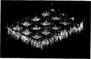
Fig. 4 a is the three-D profile of measuring by the optical profile of the typical miniature cup of little mold pressing made.Fig. 4 b is the light micrograph vertical view of this miniature cup opening of expression.Fig. 4 c is the optical profile longitudinal profile view of a row miniature cup of its degree of depth of expression.
I (b) makes miniature cup by graph exposure
As the method that another kind is made miniature cup, can utilize the radiation of ultraviolet light or other form, pass photomask (50), will be coated on radiation curing material (51) on the conducting film (52) and carry out graph exposure (Fig. 5 is a).This conducting film (52) is coated on the plastic base (53).
With regard to roll-to-roll technology, photomask can be synchronous with web, promptly moves with the speed identical with web.In the photomask (50) of Fig. 5 a, dark square (54) is represented opaque zone, and the space between this darkened boxes (55) then represent unscreened zone.Ultraviolet light passes unscreened zone (55) and is radiated on the radiation curing material.Through the exposed areas hardening, then unexposed area (zone of opacity of photomask is protected) is removed with appropriate solvent or developer, form miniature cup (56).This solvent or developer are selected from the material that butanone, toluene, acetone, isopropyl alcohol or analog etc. are generally used for dissolving or reducing radiation curing material viscosity.
Fig. 5 b and Fig. 5 c explanation prepare other two kinds of optional methods of miniature cup with graph exposure.These two illustrated characteristics are basic identical with Fig. 5 a, and corresponding assembly is also used identical figure denote.In Fig. 5 b, the opaque and prefabricated figure of employed conducting film (52).In this case, it is favourable utilizing conductive pattern as photomask photosensitive material to be carried out graph exposure.Behind ultraviolet radiation, remove unexposed area, make miniature cup (56).In Fig. 5 c, conducting film (52) also is opaque and district's band picture case is arranged.Make this radiation curing material exposure from the bottom by district's band pattern conducting film (52) as first photomask.By having patterned second photomask in the district vertical (50), carry out second exposure from opposite side with district's band of this conducting film.Remove unexposed area with solvent or developer then, manifest miniature cup (56).
Usually, this miniature cup can be an arbitrary shape, and its size and shape can change.In a system, this miniature cup can have roughly the same size and dimension.Yet,, can make the different mixing miniature cup of shape and size in order to make the optical effect maximization.For example, can have different shapes or size with green miniature cup or blue miniature cup with the red miniature cup that disperses thing to fill.In addition, pixel can be made up of the miniature cup of the different colours of different numbers.For example, a pixel can be made up of a plurality of little green miniature cups, a plurality of big red miniature cup and a plurality of little blue miniature cup.Three kinds of colors needn't be of similar shape and number.
The opening of this miniature cup can be circle, square, rectangle, sexangle or any other shape.Interval region between the opening is preferably smaller, so that when keeping desirable engineering properties, obtains higher color saturation and contrast.Therefore, other shape of honeycomb aperture efficiency (for example circular) opening is better.
For reflective electrophoretic display device (EPD), the size of each miniature cup can be about 10
2To about 5 * 10
5In the scope of square micron, be preferably about 10
3To about 5 * 10
4Square micron.The degree of depth of miniature cup is preferably about 10 to about 50 microns about 3 to about 100 microns scope.Opening about 0.05 to about 100 scope, is preferably about 0.4 to about 20 to the ratio of wall.The distance of opening (by the distance at edge to the edge of opening) is usually about 15 to about 450 microns scope, preferred about 25 to about 300 microns.
The preparation of II suspension/dispersion thing
Fill miniature cup with the charged pigment particles that is dispersed in the dielectric solvent.This disperses thing for example to be disclosed in United States Patent (USP) the 6th, 017 according to existing method preparation, No. 584, the 5th, 914, No. 806, the 5th, 573, No. 711, the 5th, 403, No. 518, the 5th, 380, No. 362, the 4th, 680, No. 103, the 4th, 285, No. 801, the 4th, 093, No. 534, the 4th, 071, No. 430, the 3rd, 668, No. 106, Institute of Electrical and Electric Engineers proceedings " electronic installation " (IEEETrans.Electron Device), ED-24,827 (1977), and J.Appl.Phys.49 (9), 4820 (1978).The medium that this charged pigment particle and its suspended visually presents a contrast.This medium is a dielectric solvent, preferably has low viscosity and specific inductive capacity about 2 to about 30, for high particulate mobility, is preferably about 2 to about 15.The embodiment of suitable dielectric solvent includes hydrocarbons such as decahydronaphthalenes (DECALIN), 5-ethylidene-2-norborene, fat oil, sweat oil; Aromatic hydrocarbonses such as toluene, dimethylbenzene, phenyl dimethylbenzene ethane, dodecyl benzene and alkyl naphthalene; Perfluorodecalin, perfluor toluene, perfluor dimethylbenzene, dichloride benzotrifluoride (dichlorobenzotrifluoride), 3,4,5 tri-chlorination-benzotrifluoride (3,4,5-trichlorobenzotrifluoride), halogenated solvent such as chlorine five fluorine-based benzene (chloropentafluoro-benzene), two chlorononanes, pentachlorobenzene; Perfluoro solvent from the 3M company of Sao Paulo, the Minnesota State (St.Paul), for example FC-43, FC-70 and FC-5060; Rein in the low-molecular-weight halogen-containing polymkeric substance of the TCI America company of state, hilllock Portland (Portland) from Russia, for example poly(perfluoropropene) base ether (poly (perfluoropropylene oxide); From the polychlorotrifluoroethylene poly (chlorotrifluoroethylene) of the Halocarbon Product company of New Jersey this e of River E, for example halocarbon oil (Halocarbon oil); Perfluorinate poly alkyl ether (perfluoropolyalkylether) is for example from the Galden of Ausimont company or from Krytox Oils and the grease K-fluid series of Delaware State DuPont.In a preferred embodiment, use polychlorotrifluoroethylene as dielectric solvent.In another preferred embodiment, use poly(perfluoropropene) base ether as dielectric solvent.
This suspending medium can be dyestuff or pigment institute is painted.Nonionic azo and anthraquinone dye are useful especially.The example indefiniteness ground of useful dyestuff comprises: the oil red EGN (Oil Red EGN) that PylamProducts company in Arizona State produces, tonyred (SudanRed), the Sudan's indigo plant (Sudan Blue), solvent blue (Oil Blue), Macrolex Blue, solvent blue 35 (Solvent Blue 35), the PylamSpirit of Arizona State Pylam Products company is black and Fast Spirit is black, the Sudan black B of Aldrich company (Sudan B1ack B), the Thermoplastic Black X-70 of BASF AG, and the anthraquinone blue of Aldrich company, anthraquinone Huang 114, anthraquinone is red 111,135, anthraquinone green 28.For the situation of insoluble pigment, be used for making the colorific granules of pigments of medium also can be scattered in this dielectric media.These coloured particles are preferably uncharged.If it is charged being used at the colorific granules of pigments of medium, then it is preferably with the electric charge opposite with this charged pigment particles.If two kinds of pigment particles have identical electric charge, then it should have different electric density or different electrophoresis rate travels.Under any circumstance, the dyestuff or the pigment that are used to produce medium color must have chemical stability, and with suspension in other component compatibility.
This charged pigment particles can be organic or inorganic pigment, as the TiO from the Sun chemical company
2, phthalocyanine blue (phthalocyanine blue), phthalocyanine green (phthalocyaninegreen), diarylide yellow (diarylide yellow), diaryl AAOT Huang (diarylideAAOT Yellow), quinacridone (quinacridone), azo (azo), rhodamine (rhodamine), perylene pigment (perylene pigment series); From hansa yellow G (the Hansa yellow G) particle of Kanto chemical company, and the carbon of Fisher company dim (Carbon Lampblack).Subparticle size preferably.This particulate should have acceptable optical characteristics, should not expanded by dielectric solvent or softening, and should be chemically stable.Under normal condition of work, the suspension that is produced also must be stablized and energy antisolvent precipitation, emulsification or condense.
This pigment particle can itself have electric charge, maybe can use charge control agent to make it obviously charged, or obtains electric charge when being suspended in the dielectric solvent.Suitable charge control agent is that the present technique field is known; They can be polymerization or non-polymeric character, also can be ionization or nonionicization, comprise ionic surface active agent, gasoloid o-tolidine (Aerosol OT) for example, neopelex, metallic soap, polybutylene succinimide, maleic anhydride multipolymer, vinylpyridine copolymer, nvp copolymer (for example from International Special Products Ganex), (methyl) acrylic copolymer, N, N-dimethyl amido ethyl (methyl) ethyl acrylate (N, N-dimethylaminoethyl (meth) acrylate) multipolymer.Fluorinated surfactant is particularly useful as charge control agent in the perfluocarbon solvent.These have comprised the FC fluorinated surfactant, for example from FC-170C, FC-171, FC-176, FC430, FC43 1 and the FC-740 of 3M company, and the Zonyl fluorinated surfactant, for example from Zonyl FSA, FSE, FSN, FSN-100, FSO, FSO-100, FSD and the UR of Dupont company.
Suitable charged pigment disperses that thing can comprise grinding by any known method manufacturing, mills, ball milling, airflow milling (microfluidizing) and ultrasonic technology.For example, the pigment particle of fine-powder form is added in this suspended solvents, formed potpourri is through ball milling or grind a few hours, and highly the dry colour powder of reunion is ground into initial particulate.Though be not preferable methods, in mechanical milling process, the dyestuff or the pigment that are used for producing the suspending medium color can add this suspension to.
Can to eliminate the precipitation or the emulsification of pigment particle, make its proportion consistent by using suitable polymkeric substance with this particulate microencapsulation with the proportion of dielectric solvent.Available chemistry or physical method are finished the microencapsulation of pigment particle.Typical encapsulation process comprises interfacial polymerization, in-situ polymerization, is separated, cohesion, electrostatic applications, spray drying, fluidized bed coating and solvent evaporation.
With regard to the electrophoretic display device (EPD) of black/white, this suspension comprises the charged white titania (TiO that is scattered in the black solvent
2) particulate, or be scattered in electrically charged black particle in a kind of dielectric solvent.Black dyes or dye mixture can be used to produce the black of solvent, Pylam Spirit as Pylam Products company (Arizona State) is black black with FastSpirit, the Sudan black B of Aldrich company, the Thermoplastic BlackX-70 of BASF AG, or a kind of insoluble black pigment such as carbon black.For other colored suspension thing, multiple possibility is arranged.For subtractive color system, charged titania (TiO
2) particulate can be suspended in the dielectric solvent of blue-green, yellow or magenta.This blue-green, yellow or magenta can use dyestuff or pigment to produce.For additive color system, charged titanium dioxide fine particles can be suspended in redness, green or the blue dielectric solvent, wherein should redness, green or blueness also can use dyestuff or pigment to produce.This redness, green or blue system are preferably adopted in most application.
III. the sealing of miniature cup
The sealing of miniature cup can be finished by several different methods.A kind of preferable methods is that the uv-curable component that will include multi-functional acrylate, acrylic acid oligomer and light trigger is dispersed in the electrophoretic fluid that includes charged pigment particles and dyed dielectric solvent.This uv-curable component and this dielectric solvent are immiscible, and its proportion is lower than this dielectric solvent and pigment particle.These two components (uv-curable component and electrophoretic fluid) are radially mixed in the mixer fully at one, and adopt accurate coating machinery devices such as Myrad rod, gravure plate, wing, fluting coating or the coating of cracking, be applied to immediately on this miniature cup.Unnecessary fluid strikes off with scraper or similar device.A spot of Weak solvent or solvent mixture example can be used to clean residual electrophoretic fluid on the partition wall top surface of this miniature cup as isopropyl alcohol, methyl alcohol or other aqueous solution solvents.Volatile organic solvent can be used to control the viscosity and the spreadability of this electrophoretic fluid.To dry through the miniature cup of filling then, and this uv-curable component floats to the top of this electrophoretic fluid.By float at this floating uv-curable layer to the surface top during or afterwards, with its curing, seal this miniature cup.Ultraviolet light or visible light, infrared ray, and the radiation of other forms such as electron beam may be used to this miniature cup is solidified and sealing.In addition, heat or moisture also can be used for this miniature cup is solidified and sealing, if suitable, can use heat or moisture-curable component.
Preferred dielectric solvent group (have desirable density, and acrylate monomer and oligomer are had desirable difference in solubility) is halocarbon hydride and derivant thereof.Surfactant can be in order to viscosity and the wetting state that improves interface between this electrophoretic fluid and the encapsulant.Useful surfactant comprises that FC surfactant, the Zonyl fluorinated surfactant of DuPont company, fluorinated acrylic ester, fluorinated methyl acrylate, the fluorine of 3M company replace the long-chain carboxylic acid and the derivant thereof of long-chain alcohols, perfluor replacement.
In addition, if this sealing precursor is compatible with dielectric solvent at least in part, then electrophoretic fluid and sealing precursor can be coated miniature cup successively.Like this, can be by coating one deck thermoset precursors thing thin layer (this precursor is that radiation, heat, moisture or interfacial reaction are curable), and it is solidified in the miniature cup surface through filling, to finish seal process.Carry out ultraviolet light polymerization after the interfacial polymerization, very favourable for seal process.Form a thin separate layer by interfacial polymerization, make electrophoretic layer and being inhibited mutual the mixing significantly between the outer coating.Then finish sealing, be preferably ultraviolet radiation or other optical radiation by the back curing schedule.For further reducing the degree of mixing mutually, preferably the proportion of outer overlay is starkly lower than the proportion of electrophoretic fluid.Available volatile organic solvent is adjusted the viscosity and the thickness of coating.Outside volatile solvent is used for during overlay, preferably with the not miscible volatile solvent of this dielectric solvent.This two step coating methods are dissolved in thermoset precursors principle shape particularly suitable at least in part to used dyestuff.
IV. the preparation of monochromatic electrophoretic display
By this technology of flowchart text shown in Figure 6.All miniature cups all use the suspension of homochromy component to fill.This technology can be continuous roll-to-roll technology, comprises the following steps:
1. go up non-essential thermoplasticity or the thermoset precursors thing (60) that has solvent of coating one deck at a conducting film (61).If solvent is arranged, then this solvent is easy to volatilization.
2. under the glass temperature that is higher than this thermoplasticity or thermoset precursors thing layer, this thermoplasticity or thermoset precursors thing layer are carried out mold pressing by a preformed punch (62).
With mould from thermoplasticity or thermoset precursors thing pull-up mould, preferably the sclerosis during or afterwards.
4. the miniature cup that will make like this (63) array is filled with dyed dielectric solvent (64), and wherein this dielectric solvent includes at least a immiscible and have than this solvent and the little thermoset precursors thing of pigment particle proportion with this solvent.
This thermoset precursors thing separate and the liquid phase top form a superposed layer during or afterwards, preferred ultraviolet radiation (65), perhaps use heat or moisture, the thermoset precursors thing is solidified and seal this miniature cup, the sealing electrophoresis cartridge that is dispersed in the pigment suspension thing in the dyed dielectric solvent is equipped with in formation like this.
6. second conducting film (66) that precoating is furnished with a glue-line (67) is layered on the electrophoresis cartridge array of sealing, and wherein this glue-line (67) can be contact adhesive, hotmelt, heat, moisture or radiation-curing binders.
If should this top conductive layer be transparent, then this stacked bonding agent can carry out back curing through this top conducting film by ultraviolet light radiation such as (68).After this stacked step is finished, just can be cut into finished product (69).
Above-mentioned miniature cup preparation can replace with another kind of method at an easy rate: the conducting film that is coated with the thermoset precursors thing is carried out graph exposure, with appropriate solvent this unexposed area is removed then.Also can be by directly coating and solidify one deck thermoset precursors thing component and finish sealing to miniature cup on electrophoretic fluid surface.
V. the preparation of multiple colour electrophoretic display
For making the multiple colour electrophoretic display, need additional step to comprise the miniature cup of different colours suspension with generation.These additional steps comprise: (1) is layered in a positivity action dry film photoresist on the Manufactured miniature cup, wherein this photoresist includes a kind of carrier of removing at least, (the Worcester of Saint-Gobain company for example, MA) PET-4851, the phenolic aldehyde positive photoresist Microposit S1818 of Shipley company, and the potpourri of the Carboset 515 of the Nacor72-8685 of National Starch company and BF Goodrich company-a kind of alkaline development glue-line; (2) by this photoresist is carried out graph exposure, removable carrier film is removed, and with diluted Microposit 351 developers of for example Shipley company this positive photoresist is developed, optionally open this miniature cup of some; (3) fill the miniature cup that this has been opened with the dyestuff or the pigment of the electrophoretic fluid that contains electrically charged Chinese white (titania) particulate and this first primary colors; And (4) according to the method for making in the monochrome display, with this miniature cup sealing through filling.These extra steps can repeat, so that make second and the three primary colors electrophoretic fluid miniature cup of filling.
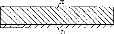
More particularly, the multiple colour electrophoretic display can be made according to step shown in Figure 7.
1. go up coating one deck thermoset precursors thing (70) at a conducting film (71).
2. under the glass temperature that is higher than thermoplasticity or thermoset precursors thing layer, this thermoplasticity or thermoset precursors thing layer are carried out mold pressing by a preformed punch (not shown).
With mould from thermoplasticity or thermoset precursors thing pull-up mould, preferably by hardening by cooling, or by radiation, heat or moisture carry out crosslinked sclerosis during or afterwards.
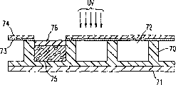
4. a stacked positive dry film photoresist is on made miniature cup (72) array, and wherein this photoresist layer comprises that at least one glue-line (73), a positive photoresist layer (74) and can go removes plastics screening glass (not shown).
5. this positive photoresist is carried out graph exposure (Fig. 7 c) with ultraviolet light, visible light or other radiation, remove the plastics screening glass, develop in the exposure area and open miniature cup.The purpose of step 4 and step 5 is to open miniature cup (Fig. 7 d) selectively in a presumptive area.
6. disperse thing (75) to fill the miniature cup that this is opened with the electrically charged Chinese white that is dispersed in the dielectric solvent, wherein this dielectric solvent comprises the dyestuff or the pigment of this first primary colors at least, and immiscible and have than this solvent and the low thermoset precursors thing (76) of pigment particle proportion with this solvent.
This thermoset precursors thing separate and form one swim in the superficial layer on this liquid phase top during or afterwards, by being solidified, this thermoset precursors thing (preferably passes through ultraviolet radiation, method by heat or moisture is taken second place) this miniature cup sealing, thus formation contains the sealing electrophoresis cartridge (Fig. 7 e) of the electrophoretic fluid of this first primary colors.
8. can repeat above-mentioned step 5 to 7, thereby produce the clearly box (Fig. 7 e, 7f and 7g) of definition that includes the different colours electrophoretic fluid in zones of different.
9. precoating is furnished with a prefabricated figure of a glue-line (78) second pre-nesa coating (77) alignment, be laminated on the electrophoresis cartridge array of sealing, its mesoglea (78) can be a contact adhesive, hotmelt, heat, moisture or radiation-curing binders.
10. this bonding agent is solidified.
The making of this miniature cup can easily replace with another kind of method in the above method: the conducting film that will be coated with a thermoset precursors thing carries out graph exposure, with appropriate solvent this unexposed area is removed then.The sealing of this miniature cup can also by directly be coated with on the liquid phase surface and cured thermoset precursor material finish.
Display with this method manufacturing can reach the only thickness of a piece of paper.The width of this display can be the width (being generally 3 to 90 inches) of coated sheets.The length of this display can be several inches to thousands of feet, depends on the size of volume.
Embodiment
Below described embodiment, be can more clearly understand and implement the present invention for ease of those skilled in the art, should not be construed as and limit the scope of the present invention, and only be explanation of the present invention and demonstration.
Embodiment 1 utilizes the miniature cup preparation of little die pressing
Component shown in the table l is nickel chromium triangle bird type (Nickel Chrome bird type) the film coated device with one 3 mil (mil) opening, and it is coated on the MylarJ101/200.Make solvent evaporates, stay the adhesive membrane that one deck glass temperature is lower than room temperature.
Table 1: the component that contains polymethylmethacrylate (PMMA) that is used for little mold pressing
| Numbering | Explanation | Composition | The supplier | Percentage by weight |
| 1 | Epoxy acrylate | Ebecryl 3605 | UCB Chemicals | 7.35 |
| 2 | Monomer | Sartomer SR205 | Sartomer | 9.59 |
| 3 | The urethanes acrylate | Ebecryl 6700 | UCB Chemicals | 4.87 |
| 4 | Polymethylmethacrylate | Elvacite 2051 | ICI | 9.11 |
| 5 | Light trigger | Darocur 1173 | Ciba | 1.45 |
| 6 | Cation light initiator | Cyracure UVI 6976 | Union Carbide | 0.60 |
| 7 | Solvent | Acetone | Aldrich | 67.03 |
| Sum | 100.00 |
Use Colorado Spring, the punch that the preform template of Photo Stencil company is used as this little mold pressing, the Frekote 700-NC that uses Henkel company is as remover.Then, the template with pressure roller is carried out mold pressing to this film through coating under the room temperature.Then, will be coated with thing through the Mylar film and carry out ultraviolet light polymerization about 20 minutes with Loctite Zeta 7410 exposure devices of metal fluoride fluorescent tube (intensity with 80 milliwatt/square centimeters, wavelength are 365 nanometers) are housed.Then will be through film demoulding from mould of mold pressing, present the clearly miniature cup of definition, measure and the microscope measurement by optical profile, this miniature cup has the lateral dimension of (200-400dpi (point/inch)) scope from 60 microns to 120 microns, and 5 microns degree of depth to 30 micrometer ranges (Fig. 4 a to Fig. 4 c).
Embodiment 2
It is as shown in table 2 to contain solid-state oligomer, monomer and components of additives.The glass temperature of this potpourri also is lower than room temperature.As precedent, this viscous coating is deposited on the top of MylarJ101/200.Mold pressing can be used heating and pressurizing roller or laminator (laminator), carries out at 32 ℃ and 60 ℃.Make and have 5 to 30 microns dark clearly high resolution micro cups (100 to 400dpi) of definition.
Table 2: the mold pressing component that contains oligomer, monomer, adjuvant and solvent
| Numbering | Explanation | Composition | The supplier | Percentage by weight |
| 1 | Epoxy acrylate | Ebecryl 3903 | UCB Chemicals | 17.21 |
| 2 | Monomer | HDODA | UCB Chemicals | 8.61 |
| 3 | The urethanes acrylate | Ebecryl 4827 | UCB Chemicals | 2.87 |
| 4 | Light trigger | Irgacure 500 | Ciba | 1.43 |
| 5 | Slip agent | Ebecryl 1360 | UCB Chemicals | 1.60 |
| 6 | Solvent | Acetone | Aldrich | 68.26 |
| Sum | 100.00 |
The preparation of the pigment dispersing thing in embodiment 3 dielectric solvents
Polystyrene (0.89 gram, Polysciences company, molecular weight 50,000) and AOT (0.094 gram, American Cyanamide company, dioctyl sodium sulfosuccinate) are dissolved in the hot dimethylbenzene (Aldrich company) of 17.77 grams.Add Ti-Pure R-706 (6.25 gram) in this solution, and the speed with 200 rev/mins (rpm) is ground more than 12 hours in a muller.Low viscosity, stable dispersion thing have been obtained.(0.25 restrains, and Aldrich) adds in this dispersion thing and dyes with solvent blue N.Then with of electrophoresis cartridge (include the two piece ITO current-carrying plates of by one 24 micron the sept being isolated) test of this suspension with a standard.Under 80 volts, can be observed the white blue alternating image of high-contrast, this image has the time of appearing in one's mind of about 60 hertz switching rate and 8.5 milliseconds.
Embodiment 4
Repeat the experiment of embodiment 3, difference is to use oil red EGN (Oil RedEGN, Aldrich company) and has the electrophoresis cartridge of 24 microns septs.Under 60 volts, can be observed the redness and the white alternating image of high-contrast, this image has the time of appearing in one's mind of about 60 hertz switching rate and 12 milliseconds.
Embodiment 5
In solution, grind Ti-Pure R-706 (112 gram) with muller, wherein this solution includes 3 of 11.2 maleic anhydride multipolymers (X-5231 of Baker Hughes) that restrain, 24 grams, 4-two chlorobenzotrifluorides (3,4-dichlorobenzotrifluoride, from Aldrich) and 24 the gram 1,6-dichloro hexane (also from Aldrich).Similarly, the carbon black of 12 grams grinds in 100 ℃ solution, this solution contains 3 of 1.2 alkylated polyvinyl pyrrolidones (alkylated polyvinylpyrrolidone) (from the Ganex of ISP V216) that restrain, 34 grams, 1 of 4-two chlorobenzotrifluorides and 34 grams, 6-dichloro hexane (Aldrich).Then, disperse things to mix equably with these two kinds and test.Under 100 volts, can be observed the black and the white alternating image of high-contrast, this image has the switching rate of the highest 10Hz and about 36 milliseconds appears the time in one's mind.
Embodiment 6 usefulness one-step technologies seal miniature cup
0.05 the 1,6 hexanediol diacrylate (HDDA that contains the benzil dimethyl ketal (benzildimethyl ketal, the Esacure KB1 of Sartomer company) that accounts for weight ratio 1% of milliliter, 1,6-hexanediol diacrylate is from Aldrich) the uv-curable component, be dispersed in 0.4 milliliter the dielectric solution, this dielectric solution contains to be dispersed in and accounts for 2,2 of weight ratio 0.5% among the FC-43 (from 3M company), 3,3,4,4,5,5,6,6,7,7,8,8,9,9,10,10,10-fluoro nonadecane-1-decyl alcohol (nonadecafluoro-1-decanol) (Aldrich).The dispersion thing that is produced is filled in the miniature cup array of making by embodiment 2 immediately.Unnecessary fluid strikes off with scraper.This HDDA solution is separated need at least 30 seconds, and are cured about 1 minute with ultraviolet radiation (10 milliwatt/square centimeter).Can observe a hard thin layer clearly at the miniature cup top, and this miniature cup is sealed.
Embodiment 7 usefulness two step methods (coating and ultraviolet light polymerization) process seal miniature cup
The electrophoretic fluid of preparation among the embodiment 5 is coated on the miniature cup array of making by embodiment 2 methods.A Norland optical adhesive NOA 60 (the Norland Products company of New Jersey NewBrunswick) thin layer is coated on this miniature cup through filling.Any unnecessary ultraviolet light bonding agent will strike off with the thin scraping blade of Mylar film, and clears up with a slice absorption paper.This bonding agent through coating carries out solidifying in 15 minutes immediately under Loctite Zeta ultraviolet photoetching device.This miniature cup is sealed fully, just looks at less than bubble.With the thickness instrumentation amount of Mitutoyo company, this bondline thickness through solidifying is about 5 to 10 microns.
Embodiment 8 usefulness two step methods (coating and moisture-curable) process seal miniature cup
Repeat the experiment of embodiment 7, difference is with alternative this Norland bonding agent of the Instant Krazy glue of Ohio Columbus Elmer ' sProducts company.The bonding agent of coating was with airborne moisture-curable 5 minutes.This miniature cup is completely sealed, and can't see bubble.With the thickness instrumentation amount of Mitutoyo company, this bondline thickness through solidifying is about 5 to 10 microns.
Embodiment 9 usefulness two step methods (coating and interfacial polymerization) process seal miniature cup
Repeat the experiment of embodiment 8, difference is with containing 3 of the tetren (Aldrich) that accounts for weight 0.3%, 4-two chlorobenzotrifluorides (3,4-dichlorobenzotrifluoride) solution replaces this electrophoretic fluid, replaces this Instant Krazy glue with the aliphatic polymeric isocyanate in the absolute ether (from the desmodur N 3300 of Bayer company) solution.After coating, almost can observe a highly cross-linked film immediately.After ether at room temperature evaporated, this dielectric solution was completely sealed in miniature cup.Do not observe bubble.
Though the present invention is by illustrating with reference to its certain specific embodiments, to those skilled in the art, can easily carries out various changes and be equal to displacement and do not depart from purpose of the present invention, spirit and scope above-mentioned embodiment.In addition, many modifications can be arranged being applicable to special situation, material, component, method, method step or step, and not break away from purpose of the present invention, spirit and scope.All these classes are revised and are considered within the scope of the appended claims.
The element numbers explanation
10 battery lead plates
11 battery lead plates
12 box layers
20 punch
2 nesa coatings
22 thermoplasticity or thermoset precursors thing layer
23 miniature cup arrays
24 webs
30 glass substrates
31 seed thin metal layers
32 photoresist layers
33 nickel cobalt (alloy)s
34 photomasks
50 photomasks
51 radiation curing materials
52 conducting films
53 plastic bases
The square of 54 dark colors
55 unscreened zones
56 miniature cups
60 thermoset precursors thing layers
61 conducting films
62 punch
63 miniature cups
64 dielectric solvents
65 ultraviolet radiations
66 second conducting films
67 glue-lines
68 ultraviolet lights (UV) radiation
69 cuttings
70 thermoset precursors things
71 conducting films
72 miniature cups
73 glue-lines
74 positive photoresists
75 pigment dispersing things
76 thermoset precursors things
77 nesa coatings
78 glue-lines
Claims (54)
1. electrophoretic display device (EPD), described electrophoretic display device (EPD) comprises a plurality of boxes, each described box comprises:
I) partition wall;
II) electrophoresis component, described electrophoresis component comprises the charged pigment particles that is dispersed in a kind of dielectric solvent or the solvent mixture;
III) polymeric seal layer, described polymeric seal layer is formed by a kind of seal group branch, and the proportion of described sealing component is lower than the proportion of described electrophoresis component, so that described electrophoresis component is sealed in each box.
2. electrophoretic display device (EPD) according to claim 1, wherein said box have basically size and shape uniformly.
3. electrophoretic display device (EPD) according to claim 1, wherein said a plurality of boxes are made up of the different box of size and dimension.
4. electrophoretic display device (EPD) according to claim 1, wherein said box right and wrong sphere.
5. electrophoretic display device (EPD) according to claim 1, wherein said box is 10 by aperture area
2To 5 * 10
5Miniature cup in the square micron scope constitutes.
6. electrophoretic display device (EPD) according to claim 5, wherein said aperture area are 10
3To 5 * 10
4Square micron.
7. electrophoretic display device (EPD) according to claim 1, wherein said box are to be that circle, polygon, sexangle, rectangle or foursquare miniature cup constitute by opening shape.
8. electrophoretic display device (EPD) according to claim 1, the degree of depth of wherein said box is 3 to 100 microns scope.
9. electrophoretic display device (EPD) according to claim 8, the wherein said degree of depth is 10 to 50 microns scope.
10. electrophoretic display device (EPD) according to claim 1, the ratio of the opening of wherein said box and box wall about 0.05 to about 100 scope.
11. electrophoretic display device (EPD) according to claim 10, wherein said ratio are 0.4 to 20.
12. electrophoretic display device (EPD) according to claim 1, wherein the described box of selecting in predetermined zone is filled by the electrophoresis component, and described electrophoresis component comprises the dielectric solvent that is dispersed in the chosen in advance color or the Chinese white in the solvent mixture.
13. electrophoretic display device (EPD) according to claim 1, the specific inductive capacity of wherein said dielectric solvent or solvent mixture is in about 2 to 30 scopes.
14. electrophoretic display device (EPD) according to claim 13, wherein said specific inductive capacity is in 2 to 10 scopes.
15. electrophoretic display device (EPD) according to claim 1, wherein said electrophoresis component comprise be dispersed in by the pigment dispersing thing of a kind of dyestuff or second kind of color the Chinese white particulate in the painted described dielectric solvent.
16. electrophoretic display device (EPD) according to claim 15, the dispersing of pigments thing of wherein said dyestuff or second kind of color is a nonionic, perhaps has and the different charge polarity of described electrophoresis component.
17. electrophoretic display device (EPD) according to claim 15, wherein said Chinese white particulate is a titanium dioxide fine particles.
18. electrophoretic display device (EPD) according to claim 1, the color of wherein said suspension are a kind of losing lustre or additive color system.
19. electrophoretic display device (EPD) according to claim 1, wherein said polymeric seal layer is formed by a kind of seal group branch, described seal group branch comprises that a kind of material is selected from: multivalence acrylate or methacrylate, cyanoacrylate, the multivalence vinyl compound, multivalence epoxide, polyvalent isocyanate, multivalence allylate and comprise the oligomer or the polymkeric substance of crosslinkable functionality.
20. electrophoretic display device (EPD) according to claim 1, the wherein said sealing component that is used to form described polymeric seal layer also comprises a kind of polymkeric substance or oligomer.
21. electrophoretic display device (EPD) according to claim 20, wherein said polymkeric substance or oligomer are solvable in described sealing component.
22. electrophoretic display device (EPD) according to claim 19, wherein said component also comprises a kind of adjuvant.
23. electrophoretic display device (EPD) according to claim 1, wherein said a plurality of boxes are sandwiched between a top electrode plate and the bottom electrode plate, one in wherein described at least top electrode plate and the bottom electrode plate is transparent.
24. electrophoretic display device (EPD) according to claim 23, wherein said top electrode plate have sealant and watching side, described top electrode plate and sealant both are transparent.
25. electrophoretic display device (EPD) according to claim 24 wherein also comprises a glue-line between described sealant and top electrode plate.
26. electrophoretic display device (EPD) according to claim 25, wherein said glue-line are a kind of contact adhesives, hot-melt adhesive, the bonding agent of heat, moisture or radiation-curable.
27. electrophoretic display device (EPD) according to claim 25, wherein said sealant and glue-line are formed by different material.
28. electrophoretic display device (EPD) according to claim 25, wherein said sealant and glue-line are formed by same material.
29. electrophoretic display device (EPD) according to claim 28, wherein said material are a kind of radiation curing materials.
30. electrophoretic display device (EPD) according to claim 23, wherein the bottom electrode plate at described sealant opposite side is to watch side, and described bottom electrode plate is transparent.
31. electrophoretic display device (EPD) according to claim 30 wherein also is included in a glue-line between described sealant and the top electrode plate.
32. electrophoretic display device (EPD) according to claim 31, wherein said glue-line are a kind of contact adhesives, hot-melt adhesive, the bonding agent of heat, moisture or radiation curing.
33. electrophoretic display device (EPD) according to claim 31, wherein said sealant and glue-line are formed by different materials.
34. electrophoretic display device (EPD) according to claim 31, wherein said sealant and glue-line are formed by same material.
35. electrophoretic display device (EPD) according to claim 34, wherein said material are a kind of radiation curing materials.
36. electrophoretic display device (EPD) according to claim 1, wherein said electrophoresis component partly is filled in each described box.
37. electrophoretic display device (EPD) according to claim 36, wherein partially filled described electrophoresis component part contacts with the polymeric seal layer.
38. a method that is used to prepare electrophoretic display device (EPD), described method may further comprise the steps:
A) fill miniature cup with the dispersion thing of thermoplasticity in a kind of electrophoretic fluid or thermoset precursors thing, described electrophoretic fluid contains the charged pigment particles that is dispersed in the dielectric solvent, and the proportion of wherein said thermoplasticity or thermoset precursors thing is lower than the proportion of described dielectric solvent and charged pigment particles; And
B) solidify by the floating layer that described thermoplasticity or thermoset precursors thing are formed at described electrophoretic fluid top, the described miniature cup sealing after filling.
39. according to the described method of claim 38, wherein said thermoset precursors thing is selected from multivalence acrylate or methacrylate, cyanoacrylate, the multivalence vinyl compound, the multivalence epoxide, polyvalent isocyanate, multivalence propylene thing and comprise the oligomer or the polymkeric substance of crosslinkable functionality.
40. according to the described method of claim 38, wherein said curing is to finish by the method for solvent evaporation, interfacial reaction, moisture, heat, radiation or its combination.
41. according to the described method of claim 40, wherein said curing is to finish by the method for ultraviolet radiation.
42. according to the described method of claim 38, wherein said thermoplasticity or thermoset precursors thing and described dielectric solvent are immiscible.
43. a method that is used to prepare electrophoretic display device (EPD), described method comprises the following steps:
A) fill miniature cup with comprising the electrophoretic fluid that is scattered in the charged pigment particles in the dielectric solvent,
B) by a kind of component that comprises thermoplasticity or thermoset precursors thing is coated on the described electrophoretic fluid, and with described miniature cup sealing through filling, the proportion of wherein said component is lower than the proportion of described dielectric solvent and charged pigment particles, and
C) solidify described thermoplasticity or thermoset precursors thing component.
44. according to the described method of claim 43, wherein said thermoset precursors thing component is that described volatile solvent or solvent mixture volatilize after described component is applied on the described electrophoretic fluid with a kind of volatile solvent or solvent mixture dilution.
45. according to the described method of claim 43, wherein said thermoset precursors thing is selected from multivalence acrylate or methacrylate, cyanoacrylate, the multivalence vinyl compound, the multivalence epoxide, polyvalent isocyanate, multivalence propylene thing comprises the oligomer or the polymkeric substance of crosslinkable functionality.
46. according to the described method of claim 43, wherein said curing is to finish by the method for solvent evaporation, interfacial reaction, moisture, heat, radiation or its combination.
47. according to the described method of claim 43, wherein said thermoplasticity or thermoset precursors thing and described dielectric solvent are immiscible.
48. a method that is used to make electrophoretic display device (EPD) may further comprise the steps:
A) preparation miniature cup;
B) with described miniature cup electrophoresis fluid filled, described electrophoretic fluid comprises the charged pigment particles that is scattered in the dielectric solvent;
C) the described miniature cup through filling with thermoplasticity or the sealing of thermoset precursors thing, the proportion of described thermoplasticity or thermoset precursors thing is lower than the proportion of described dielectric solvent and charged pigment particles.
49. according to the described method of claim 48, wherein said thermoplasticity or thermoset precursors thing and described dielectric solvent are immiscible.
50. according to the described method of claim 48, wherein said filling and sealing miniature cup are by filling described miniature cup with the dispersion thing of thermoplasticity in the electrophoretic fluid or thermoset precursors thing and making described thermoplasticity or floating layer curing that the thermoset precursors thing forms at described electrophoretic fluid top is finished.
51. according to the described method of claim 49, wherein said curing is to finish by the method for solvent evaporation, interfacial reaction, moisture, heat, radiation or its combination.
52. according to the described method of claim 48, the sealing of wherein said miniature cup of having filled is by coating one deck thermoplasticity or thermoset precursors thing component on described electrophoretic fluid, and described thermoplasticity or thermoset precursors thing component solidified finishes.
53. according to the described method of claim 52, wherein said curing is to finish by the method for solvent evaporation, interfacial reaction, moisture, heat, radiation or its combination.
54. according to the described method of claim 48, wherein said miniature cup is by with punch mold pressing one thermoplasticity or thermoset precursors thing layer, perhaps a radiation adjustable curing material layer is carried out graph exposure and removes that unexposed area prepares.
Applications Claiming Priority (2)
| Application Number | Priority Date | Filing Date | Title |
|---|---|---|---|
| US09/518,488 US6930818B1 (en) | 2000-03-03 | 2000-03-03 | Electrophoretic display and novel process for its manufacture |
| US09/518,488 | 2000-03-03 |
Related Child Applications (1)
| Application Number | Title | Priority Date | Filing Date |
|---|---|---|---|
| CNB2004100327522A Division CN100368922C (en) | 2000-03-03 | 2001-03-05 | Electrophoretic display and novel process for its manufacture |
Publications (2)
| Publication Number | Publication Date |
|---|---|
| CN1363056A CN1363056A (en) | 2002-08-07 |
| CN1174281C true CN1174281C (en) | 2004-11-03 |
Family
ID=24064141
Family Applications (2)
| Application Number | Title | Priority Date | Filing Date |
|---|---|---|---|
| CNB2004100327522A Expired - Fee Related CN100368922C (en) | 2000-03-03 | 2001-03-05 | Electrophoretic display and novel process for its manufacture |
| CNB018002277A Expired - Lifetime CN1174281C (en) | 2000-03-03 | 2001-03-05 | Improved electrophoretic display and novel manufacture method thereof |
Family Applications Before (1)
| Application Number | Title | Priority Date | Filing Date |
|---|---|---|---|
| CNB2004100327522A Expired - Fee Related CN100368922C (en) | 2000-03-03 | 2001-03-05 | Electrophoretic display and novel process for its manufacture |
Country Status (13)
| Country | Link |
|---|---|
| US (4) | US6930818B1 (en) |
| EP (2) | EP1264210B1 (en) |
| JP (2) | JP3680996B2 (en) |
| KR (4) | KR100566417B1 (en) |
| CN (2) | CN100368922C (en) |
| AT (1) | ATE283499T1 (en) |
| AU (1) | AU2001240036A1 (en) |
| CA (1) | CA2401564C (en) |
| DE (1) | DE60107396T2 (en) |
| HK (1) | HK1047477B (en) |
| MX (1) | MXPA02008517A (en) |
| TW (1) | TWI238917B (en) |
| WO (1) | WO2001067170A1 (en) |
Families Citing this family (356)
| Publication number | Priority date | Publication date | Assignee | Title |
|---|---|---|---|---|
| ATE356369T1 (en) * | 1996-07-19 | 2007-03-15 | E Ink Corp | ELECTRONICALLY ADDRESSABLE MICRO-ENCAPSULED INK |
| US7075502B1 (en) | 1998-04-10 | 2006-07-11 | E Ink Corporation | Full color reflective display with multichromatic sub-pixels |
| CA2330950A1 (en) | 1998-05-12 | 1999-11-18 | E Ink Corporation | Microencapsulated electrophoretic electrostatically-addressed media for drawing device applications |
| US6930818B1 (en) * | 2000-03-03 | 2005-08-16 | Sipix Imaging, Inc. | Electrophoretic display and novel process for its manufacture |
| US6933098B2 (en) | 2000-01-11 | 2005-08-23 | Sipix Imaging Inc. | Process for roll-to-roll manufacture of a display by synchronized photolithographic exposure on a substrate web |
| US7715088B2 (en) | 2000-03-03 | 2010-05-11 | Sipix Imaging, Inc. | Electrophoretic display |
| US6831770B2 (en) * | 2000-03-03 | 2004-12-14 | Sipix Imaging, Inc. | Electrophoretic display and novel process for its manufacture |
| US7052571B2 (en) * | 2000-03-03 | 2006-05-30 | Sipix Imaging, Inc. | Electrophoretic display and process for its manufacture |
| US6829078B2 (en) * | 2000-03-03 | 2004-12-07 | Sipix Imaging Inc. | Electrophoretic display and novel process for its manufacture |
| US20070237962A1 (en) * | 2000-03-03 | 2007-10-11 | Rong-Chang Liang | Semi-finished display panels |
| US7158282B2 (en) | 2000-03-03 | 2007-01-02 | Sipix Imaging, Inc. | Electrophoretic display and novel process for its manufacture |
| US7576904B2 (en) * | 2000-03-03 | 2009-08-18 | Sipix Imaging, Inc. | Electro-magnetophoresis display |
| US7142351B2 (en) * | 2000-03-03 | 2006-11-28 | Sipix Imaging, Inc. | Electro-magnetophoresis display |
| US7715087B2 (en) | 2000-03-03 | 2010-05-11 | Sipix Imaging, Inc. | Segment electrophoretic displays and methods for their manufacture |
| US6972893B2 (en) | 2001-06-11 | 2005-12-06 | Sipix Imaging, Inc. | Process for imagewise opening and filling color display components and color displays manufactured thereof |
| US7233429B2 (en) * | 2000-03-03 | 2007-06-19 | Sipix Imaging, Inc. | Electrophoretic display |
| US7557981B2 (en) * | 2000-03-03 | 2009-07-07 | Sipix Imaging, Inc. | Electrophoretic display and process for its manufacture |
| US6545797B2 (en) | 2001-06-11 | 2003-04-08 | Sipix Imaging, Inc. | Process for imagewise opening and filling color display components and color displays manufactured thereof |
| US6885495B2 (en) * | 2000-03-03 | 2005-04-26 | Sipix Imaging Inc. | Electrophoretic display with in-plane switching |
| NL1015841C2 (en) * | 2000-07-31 | 2002-02-01 | Zetfolie B V | An imaging system as well as an apparatus and method for controlling this system. |
| US8282762B2 (en) * | 2001-01-11 | 2012-10-09 | Sipix Imaging, Inc. | Transmissive or reflective liquid crystal display and process for its manufacture |
| US7471369B2 (en) * | 2001-01-11 | 2008-12-30 | Sipix Imaging, Inc. | Transmissive or reflective liquid crystal display and process for its manufacture |
| US6795138B2 (en) | 2001-01-11 | 2004-09-21 | Sipix Imaging, Inc. | Transmissive or reflective liquid crystal display and novel process for its manufacture |
| TW556044B (en) | 2001-02-15 | 2003-10-01 | Sipix Imaging Inc | Process for roll-to-roll manufacture of a display by synchronized photolithographic exposure on a substrate web |
| US7604706B2 (en) * | 2001-03-30 | 2009-10-20 | Minolta Co., Ltd. | Method for producing resin-molded substrate and method for producing reversible image display medium |
| US7230750B2 (en) * | 2001-05-15 | 2007-06-12 | E Ink Corporation | Electrophoretic media and processes for the production thereof |
| US6753067B2 (en) | 2001-04-23 | 2004-06-22 | Sipix Imaging, Inc. | Microcup compositions having improved flexure resistance and release properties |
| US20020188053A1 (en) | 2001-06-04 | 2002-12-12 | Sipix Imaging, Inc. | Composition and process for the sealing of microcups in roll-to-roll display manufacturing |
| US7205355B2 (en) | 2001-06-04 | 2007-04-17 | Sipix Imaging, Inc. | Composition and process for the manufacture of an improved electrophoretic display |
| US8361356B2 (en) * | 2001-06-04 | 2013-01-29 | Sipix Imaging, Inc. | Composition and process for the sealing of microcups in roll-to-roll display manufacturing |
| US6788452B2 (en) | 2001-06-11 | 2004-09-07 | Sipix Imaging, Inc. | Process for manufacture of improved color displays |
| US7385751B2 (en) | 2001-06-11 | 2008-06-10 | Sipix Imaging, Inc. | Process for imagewise opening and filling color display components and color displays manufactured thereof |
| TW527529B (en) * | 2001-07-27 | 2003-04-11 | Sipix Imaging Inc | An improved electrophoretic display with color filters |
| JP4155553B2 (en) * | 2001-08-01 | 2008-09-24 | キヤノン株式会社 | Display element and manufacturing method thereof |
| US7492505B2 (en) | 2001-08-17 | 2009-02-17 | Sipix Imaging, Inc. | Electrophoretic display with dual mode switching |
| US7038670B2 (en) | 2002-08-16 | 2006-05-02 | Sipix Imaging, Inc. | Electrophoretic display with dual mode switching |
| TW550529B (en) | 2001-08-17 | 2003-09-01 | Sipix Imaging Inc | An improved electrophoretic display with dual-mode switching |
| TW539928B (en) | 2001-08-20 | 2003-07-01 | Sipix Imaging Inc | An improved transflective electrophoretic display |
| TW573204B (en) | 2001-09-12 | 2004-01-21 | Sipix Imaging Inc | An improved electrophoretic display with gating electrodes |
| TWI229763B (en) | 2001-10-29 | 2005-03-21 | Sipix Imaging Inc | An improved electrophoretic display with holding electrodes |
| TWI229776B (en) | 2002-01-03 | 2005-03-21 | Sipix Imaging Inc | A novel electrophoretic dispersion with a fluorinated solvent and a charge controlling agent |
| TWI250894B (en) * | 2002-01-03 | 2006-03-11 | Sipix Imaging Inc | Functionalized halogenated polymers for microencapsulation |
| US6529313B1 (en) * | 2002-01-16 | 2003-03-04 | Xerox Corporation | Electrophoretic displays, display fluids for use therein, and methods of displaying images |
| US7123238B2 (en) * | 2002-01-16 | 2006-10-17 | Xerox Corporation | Spacer layer for electrophoretic display device |
| US6525866B1 (en) * | 2002-01-16 | 2003-02-25 | Xerox Corporation | Electrophoretic displays, display fluids for use therein, and methods of displaying images |
| US7382514B2 (en) * | 2002-02-11 | 2008-06-03 | Sipix Imaging, Inc. | Core-shell particles for electrophoretic display |
| US6885146B2 (en) | 2002-03-14 | 2005-04-26 | Semiconductor Energy Laboratory Co., Ltd. | Display device comprising substrates, contrast medium and barrier layers between contrast medium and each of substrates |
| US7580180B2 (en) | 2002-03-21 | 2009-08-25 | Sipix Imaging, Inc. | Magnetophoretic and electromagnetophoretic displays |
| TW578121B (en) | 2002-03-21 | 2004-03-01 | Sipix Imaging Inc | Magnetophoretic and electromagnetophoretic display |
| US7113323B2 (en) | 2002-03-21 | 2006-09-26 | Sipix Imaging, Inc. | Magnetophoretic and electromagnetophoretic displays |
| CN1209674C (en) | 2002-04-23 | 2005-07-06 | 希毕克斯影像有限公司 | Electromagnetic phoretic display |
| TWI223729B (en) | 2002-04-23 | 2004-11-11 | Sipix Imaging Inc | Improved segment electrophoretic displays and methods for their manufacture |
| TWI240842B (en) | 2002-04-24 | 2005-10-01 | Sipix Imaging Inc | Matrix driven electrophoretic display with multilayer back plane |
| US7307778B2 (en) | 2002-04-24 | 2007-12-11 | Sipix Imaging, Inc. | Compositions and processes for format-flexible, roll-to-roll manufacturing of electrophoretic displays |
| US7261920B2 (en) * | 2002-04-24 | 2007-08-28 | Sipix Imaging, Inc. | Process for forming a patterned thin film structure on a substrate |
| US7972472B2 (en) * | 2002-04-24 | 2011-07-05 | Sipix Imaging, Inc. | Process for forming a patterned thin film structure for in-mold decoration |
| US8002948B2 (en) * | 2002-04-24 | 2011-08-23 | Sipix Imaging, Inc. | Process for forming a patterned thin film structure on a substrate |
| TW574538B (en) | 2002-04-24 | 2004-02-01 | Sipix Imaging Inc | Compositions and processes for format flexible roll-to-roll manufacturing of electrophoretic displays |
| US7156945B2 (en) | 2002-04-24 | 2007-01-02 | Sipix Imaging, Inc. | Process for forming a patterned thin film structure for in-mold decoration |
| TWI268813B (en) * | 2002-04-24 | 2006-12-21 | Sipix Imaging Inc | Process for forming a patterned thin film conductive structure on a substrate |
| TWI310098B (en) | 2002-05-03 | 2009-05-21 | Sipix Imaging Inc | Methods of surface modification for improving electrophoretic display performance |
| TWI329662B (en) | 2002-05-17 | 2010-09-01 | Sipix Imaging Inc | Novel fluorinated silicon (iv) phthalocyanines and naphthalocyanines for electrophoretic, magnetophoretic or electromagnetophoretic display |
| TW583497B (en) * | 2002-05-29 | 2004-04-11 | Sipix Imaging Inc | Electrode and connecting designs for roll-to-roll format flexible display manufacturing |
| EP1389487B1 (en) | 2002-07-16 | 2006-05-03 | Seiko Epson Corporation | Microcapsule composition for electrophoretic displays |
| US7347957B2 (en) * | 2003-07-10 | 2008-03-25 | Sipix Imaging, Inc. | Methods and compositions for improved electrophoretic display performance |
| TWI314237B (en) * | 2002-07-17 | 2009-09-01 | Sipix Imaging Inc | Novel methods and compositions for improved electrophoretic display performance |
| US8547628B2 (en) | 2002-07-17 | 2013-10-01 | Sipix Imaging, Inc. | Methods and compositions for improved electrophoretic display performance |
| US20060255322A1 (en) * | 2002-07-17 | 2006-11-16 | Wu Zarng-Arh G | Methods and compositions for improved electrophoretic display performance |
| US20040105036A1 (en) * | 2002-08-06 | 2004-06-03 | E Ink Corporation | Protection of electro-optic displays against thermal effects |
| US7271947B2 (en) | 2002-08-16 | 2007-09-18 | Sipix Imaging, Inc. | Electrophoretic display with dual-mode switching |
| US7038656B2 (en) | 2002-08-16 | 2006-05-02 | Sipix Imaging, Inc. | Electrophoretic display with dual-mode switching |
| JP4337439B2 (en) | 2002-08-22 | 2009-09-30 | セイコーエプソン株式会社 | Electrophoresis equipment, electronic equipment |
| US7166182B2 (en) * | 2002-09-04 | 2007-01-23 | Sipix Imaging, Inc. | Adhesive and sealing layers for electrophoretic displays |
| TW575646B (en) * | 2002-09-04 | 2004-02-11 | Sipix Imaging Inc | Novel adhesive and sealing layers for electrophoretic displays |
| TWI300157B (en) * | 2002-09-10 | 2008-08-21 | Sipix Imaging Inc | Electrochromic or electrodeposition display and process for their preparation |
| TWI328711B (en) * | 2002-09-18 | 2010-08-11 | Sipix Imaging Inc | Electrophoretic display with improved temperature latitude and switching performance |
| US7616374B2 (en) * | 2002-09-23 | 2009-11-10 | Sipix Imaging, Inc. | Electrophoretic displays with improved high temperature performance |
| TWI327251B (en) * | 2002-09-23 | 2010-07-11 | Sipix Imaging Inc | Electrophoretic displays with improved high temperature performance |
| TWI293715B (en) * | 2002-10-10 | 2008-02-21 | Sipix Imaging Inc | A method for inducing or enhancing the threshold of an electrophoretic display, an electrophoretic fluid and an electrophoretic display |
| US20130063333A1 (en) | 2002-10-16 | 2013-03-14 | E Ink Corporation | Electrophoretic displays |
| US7245417B2 (en) * | 2002-10-21 | 2007-07-17 | Canon Kabushiki Kaisha | Process for producing display device |
| JP3927897B2 (en) * | 2002-10-21 | 2007-06-13 | キヤノン株式会社 | Manufacturing method of display element |
| TWI229230B (en) * | 2002-10-31 | 2005-03-11 | Sipix Imaging Inc | An improved electrophoretic display and novel process for its manufacture |
| US8023071B2 (en) * | 2002-11-25 | 2011-09-20 | Sipix Imaging, Inc. | Transmissive or reflective liquid crystal display |
| TWI297089B (en) | 2002-11-25 | 2008-05-21 | Sipix Imaging Inc | A composition for the preparation of microcups used in a liquid crystal display, a liquid crystal display comprising two or more layers of microcup array and process for its manufacture |
| US6831771B2 (en) * | 2003-01-08 | 2004-12-14 | Sipix Imaging Inc. | Electronic whiteboard using electrophoretic display |
| US7379228B2 (en) * | 2003-01-17 | 2008-05-27 | Koninklijke Philips Electroncis N.V. | Electrophoretic display |
| US7572491B2 (en) * | 2003-01-24 | 2009-08-11 | Sipix Imaging, Inc. | Adhesive and sealing layers for electrophoretic displays |
| TWI230832B (en) * | 2003-01-24 | 2005-04-11 | Sipix Imaging Inc | Novel adhesive and sealing layers for electrophoretic displays |
| US9346987B2 (en) * | 2003-01-24 | 2016-05-24 | E Ink California, Llc | Adhesive and sealing layers for electrophoretic displays |
| TWI337679B (en) | 2003-02-04 | 2011-02-21 | Sipix Imaging Inc | Novel compositions and assembly process for liquid crystal display |
| TWI228632B (en) * | 2003-02-06 | 2005-03-01 | Sipix Imaging Inc | Improved electrophoretic display with a bi-modal particle system |
| DE602004005192T2 (en) * | 2003-06-06 | 2007-11-08 | Sipix Imaging Inc., Fremont | IN-FORM MANUFACTURE OF AN OBJECT WITH EMBEDDED DISPLAY PANEL |
| EP1631857B1 (en) * | 2003-06-06 | 2007-03-07 | Sipix Imaging, Inc. | In mold manufacture of an object with embedded display panel |
| US20070091061A1 (en) * | 2003-06-13 | 2007-04-26 | Koninklijke Philips Electronics N.V. | Electrophoretic display device and method for manufacturing such a device |
| US7390901B2 (en) | 2003-08-08 | 2008-06-24 | Sipix Imaging, Inc. | Fluorinated dyes or colorants and their uses |
| US7717764B2 (en) | 2003-09-12 | 2010-05-18 | Bridgestone Corporation | Method of manufacturing image display panel and image display panel |
| US7061662B2 (en) * | 2003-10-07 | 2006-06-13 | Sipix Imaging, Inc. | Electrophoretic display with thermal control |
| US8514168B2 (en) * | 2003-10-07 | 2013-08-20 | Sipix Imaging, Inc. | Electrophoretic display with thermal control |
| US7177066B2 (en) | 2003-10-24 | 2007-02-13 | Sipix Imaging, Inc. | Electrophoretic display driving scheme |
| US7572394B2 (en) | 2003-11-04 | 2009-08-11 | Sipix Imaging, Inc. | Electrophoretic dispersions |
| US8257614B2 (en) | 2003-11-04 | 2012-09-04 | Sipix Imaging, Inc. | Electrophoretic dispersions |
| US7277218B2 (en) | 2003-11-04 | 2007-10-02 | Sipix Imaging, Inc. | Electrophoretic compositions |
| US20110164301A1 (en) | 2003-11-05 | 2011-07-07 | E Ink Corporation | Electro-optic displays, and materials for use therein |
| US8177942B2 (en) * | 2003-11-05 | 2012-05-15 | E Ink Corporation | Electro-optic displays, and materials for use therein |
| US8928562B2 (en) * | 2003-11-25 | 2015-01-06 | E Ink Corporation | Electro-optic displays, and methods for driving same |
| US7279064B2 (en) | 2003-12-18 | 2007-10-09 | Palo Alto Research Center, Incorporated | Method of sealing an array of cell microstructures using microencapsulated adhesive |
| CN100350323C (en) * | 2003-12-29 | 2007-11-21 | 漳立冰 | Flexible ultra-thin electrophoresis display screen and method for making same |
| US7504050B2 (en) * | 2004-02-23 | 2009-03-17 | Sipix Imaging, Inc. | Modification of electrical properties of display cells for improving electrophoretic display performance |
| JP4849640B2 (en) | 2004-04-08 | 2012-01-11 | サムスン エルシーディー ネザーランズ アール アンド ディー センター ビー.ブイ. | Display device |
| US7470386B2 (en) | 2004-04-26 | 2008-12-30 | Sipix Imaging, Inc. | Roll-to-roll embossing tools and processes |
| US7374634B2 (en) * | 2004-05-12 | 2008-05-20 | Sipix Imaging, Inc. | Process for the manufacture of electrophoretic displays |
| US8625188B2 (en) * | 2004-05-12 | 2014-01-07 | Sipix Imaging, Inc. | Process for the manufacture of electrophoretic displays |
| KR20070029714A (en) * | 2004-05-28 | 2007-03-14 | 코닌클리케 필립스 일렉트로닉스 엔.브이. | Flexible flat panel displays |
| ES2552373T3 (en) * | 2004-07-02 | 2015-11-27 | Essilor International (Compagnie Générale d'Optique) | Photochromic optical component |
| US7301693B2 (en) * | 2004-08-13 | 2007-11-27 | Sipix Imaging, Inc. | Direct drive display with a multi-layer backplane and process for its manufacture |
| KR100616132B1 (en) | 2004-08-24 | 2006-08-28 | 재단법인 전라남도신소재산업진흥재단 | A partition wall structure for electrophoretic display device and electrophoretic display device using the same |
| US8643595B2 (en) * | 2004-10-25 | 2014-02-04 | Sipix Imaging, Inc. | Electrophoretic display driving approaches |
| US7304780B2 (en) * | 2004-12-17 | 2007-12-04 | Sipix Imaging, Inc. | Backplane design for display panels and processes for their manufacture |
| US7463409B2 (en) | 2004-12-20 | 2008-12-09 | Palo Alto Research Center Incorporated | Flexible electrophoretic-type display |
| US20060146232A1 (en) * | 2004-12-31 | 2006-07-06 | Chi-Chang Liao | Passive matrix display and manufacture method |
| DE102005004156A1 (en) * | 2005-01-28 | 2006-08-10 | Siemens Ag | Electrophoretic display film |
| US8576162B2 (en) * | 2005-03-14 | 2013-11-05 | Sipix Imaging, Inc. | Manufacturing processes of backplane for segment displays |
| GB2425611B (en) | 2005-03-29 | 2010-03-24 | Hewlett Packard Development Co | Reflective colour display device |
| US7821700B2 (en) * | 2005-03-31 | 2010-10-26 | Mark W Miles | Dynamic motile medium |
| US8159636B2 (en) * | 2005-04-08 | 2012-04-17 | Sipix Imaging, Inc. | Reflective displays and processes for their manufacture |
| US8802214B2 (en) | 2005-06-13 | 2014-08-12 | Trillion Science, Inc. | Non-random array anisotropic conductive film (ACF) and manufacturing processes |
| US20060280912A1 (en) * | 2005-06-13 | 2006-12-14 | Rong-Chang Liang | Non-random array anisotropic conductive film (ACF) and manufacturing processes |
| US7248411B2 (en) * | 2005-06-24 | 2007-07-24 | Industrial Technology Research Institute | Optical film with array of microstructures and the light source apparatus utilizing the same |
| FR2888950B1 (en) * | 2005-07-20 | 2007-10-12 | Essilor Int | TRANSPARENT PIXELLIZED OPTICAL COMPONENT WITH ABSORBENT WALLS ITS MANUFACTURING METHOD AND USE IN FARICATION OF A TRANSPARENT OPTICAL ELEMENT |
| FR2888948B1 (en) * | 2005-07-20 | 2007-10-12 | Essilor Int | PIXELLIZED TRANSPARENT OPTIC COMPONENT COMPRISING AN ABSORBENT COATING, METHOD FOR PRODUCING THE SAME AND USE THEREOF IN AN OPTICAL ELEMENT |
| FR2888947B1 (en) | 2005-07-20 | 2007-10-12 | Essilor Int | OPTICAL CELL COMPONENT |
| KR100686870B1 (en) * | 2005-09-07 | 2007-02-26 | 엘지전자 주식회사 | Manufacturing process of electronic paper display device by offset printing |
| US7880958B2 (en) * | 2005-09-23 | 2011-02-01 | Sipix Imaging, Inc. | Display cell structure and electrode protecting layer compositions |
| US8441432B2 (en) * | 2005-09-23 | 2013-05-14 | Sipix Imaging, Inc. | Display cell structure and electrode protecting layer compositions |
| US7408699B2 (en) * | 2005-09-28 | 2008-08-05 | Sipix Imaging, Inc. | Electrophoretic display and methods of addressing such display |
| JP4586711B2 (en) * | 2005-11-09 | 2010-11-24 | セイコーエプソン株式会社 | Method for manufacturing electrophoretic display sheet and method for manufacturing electrophoretic display device |
| JP5194355B2 (en) * | 2005-11-25 | 2013-05-08 | 富士ゼロックス株式会社 | Display medium and display method |
| JP2007147829A (en) * | 2005-11-25 | 2007-06-14 | Brother Ind Ltd | Method for manufacturing partition wall and substrate in electrophoretic display medium, and electrophoretic display medium |
| TWI271390B (en) * | 2005-12-13 | 2007-01-21 | Ind Tech Res Inst | Non-mask micro-flow etching process |
| JP2007218990A (en) * | 2006-02-14 | 2007-08-30 | Toppan Forms Co Ltd | Electrophoretic display system |
| US7324264B2 (en) * | 2006-02-23 | 2008-01-29 | Eastman Kodak Company | Electro-optical modulating display and method of making the same |
| US7746541B2 (en) * | 2006-03-13 | 2010-06-29 | Honeywell International Inc. | System and apparatus for an electrophoretic display |
| US7982479B2 (en) * | 2006-04-07 | 2011-07-19 | Sipix Imaging, Inc. | Inspection methods for defects in electrophoretic display and related devices |
| KR101298296B1 (en) * | 2006-05-08 | 2013-08-20 | 엘지디스플레이 주식회사 | Fabricating method for flat panel display |
| US7280266B1 (en) * | 2006-05-19 | 2007-10-09 | Xerox Corporation | Electrophoretic display medium and device |
| US20070268446A1 (en) * | 2006-05-22 | 2007-11-22 | Shie-Chang Jeng | Liquid crystal device and method for forming the same |
| US7685967B2 (en) | 2006-05-23 | 2010-03-30 | Seed Resources, Llc | Feed cake assembly |
| US7683606B2 (en) * | 2006-05-26 | 2010-03-23 | Sipix Imaging, Inc. | Flexible display testing and inspection |
| JP2008008880A (en) * | 2006-06-02 | 2008-01-17 | Sumitomo Bakelite Co Ltd | Microchip made from plastic, manufacturing method therefor, and biochip or microanalytical chip using the same |
| CN100412677C (en) * | 2006-06-12 | 2008-08-20 | 天津大学 | Preparation of microcheck method electrophoresis display |
| US20150005720A1 (en) | 2006-07-18 | 2015-01-01 | E Ink California, Llc | Electrophoretic display |
| TWI491953B (en) * | 2006-07-18 | 2015-07-11 | Sipix Imaging Inc | Electrophoretic display |
| US8830561B2 (en) | 2006-07-18 | 2014-09-09 | E Ink California, Llc | Electrophoretic display |
| US7307779B1 (en) | 2006-09-21 | 2007-12-11 | Honeywell International, Inc. | Transmissive E-paper display |
| US8623191B2 (en) * | 2006-09-22 | 2014-01-07 | Honeywell International Inc. | Non-volatile addressable electronic paper with gray level capability |
| US7923488B2 (en) * | 2006-10-16 | 2011-04-12 | Trillion Science, Inc. | Epoxy compositions |
| DE102006052606B4 (en) * | 2006-11-08 | 2008-09-18 | Leonhard Kurz Gmbh & Co. Kg | Process for the preparation of PDLCDs |
| US7675672B2 (en) * | 2006-11-09 | 2010-03-09 | Honeywell International Inc. | Non-volatile addressable electronic paper for disposable flexible displays |
| US7843623B2 (en) * | 2006-11-16 | 2010-11-30 | Honeywell International Inc. | Non volatile addressable electronic paper with color capability |
| US7905977B2 (en) * | 2006-11-17 | 2011-03-15 | Sipix Imaging, Inc. | Post conversion methods for display devices |
| FR2910642B1 (en) * | 2006-12-26 | 2009-03-06 | Essilor Int | TRANSPARENT OPTICAL COMPONENT WITH TWO CELL ARRAYS |
| US8011592B2 (en) * | 2007-01-19 | 2011-09-06 | Sipix Imaging, Inc. | Temperature management in an integrated circuit card with electrophoretic display |
| JP4906539B2 (en) * | 2007-03-02 | 2012-03-28 | 株式会社リコー | Honeycomb structure, method for manufacturing honeycomb structure, and image display device |
| KR20090086388A (en) * | 2007-03-08 | 2009-08-12 | 가부시키가이샤 리코 | Display element, image display device, and image display system |
| JP5157200B2 (en) * | 2007-03-08 | 2013-03-06 | 株式会社リコー | Manufacturing method of honeycomb structure sheet and manufacturing method of display panel |
| JP5132168B2 (en) | 2007-03-08 | 2013-01-30 | 株式会社リコー | Manufacturing method and manufacturing apparatus for structure for image display element, and manufacturing method and manufacturing apparatus for electrophoretic display element |
| US8274472B1 (en) | 2007-03-12 | 2012-09-25 | Sipix Imaging, Inc. | Driving methods for bistable displays |
| JP2007179079A (en) * | 2007-03-29 | 2007-07-12 | Hatsumeiya:Kk | Air bubble sheet type electronic paper |
| KR100842170B1 (en) * | 2007-04-23 | 2008-06-27 | 에스케이 텔레콤주식회사 | Addressing method of particle for colorful e-paper |
| GB2448730A (en) * | 2007-04-25 | 2008-10-29 | Innos Ltd | Fabrication of Planar Electronic Circuit Devices |
| US8243013B1 (en) | 2007-05-03 | 2012-08-14 | Sipix Imaging, Inc. | Driving bistable displays |
| KR101415569B1 (en) | 2007-05-14 | 2014-07-04 | 삼성디스플레이 주식회사 | Electrophoretic display unit and display device using the same and method of manufacturing for the same |
| JP5218959B2 (en) * | 2007-06-01 | 2013-06-26 | 株式会社リコー | Electrophoretic display device, display method, method for manufacturing electrophoretic display element, and method for manufacturing electrophoretic display device |
| US20080303780A1 (en) | 2007-06-07 | 2008-12-11 | Sipix Imaging, Inc. | Driving methods and circuit for bi-stable displays |
| DE102007029566B4 (en) | 2007-06-26 | 2012-12-13 | Bundesdruckerei Gmbh | A method of making an electrophoretic display, electrophoretic display and document |
| US8743077B1 (en) | 2007-08-01 | 2014-06-03 | Sipix Imaging, Inc. | Front light system for reflective displays |
| KR100929486B1 (en) * | 2007-09-11 | 2009-12-02 | 에스케이씨하스디스플레이필름(유) | Optical element for display device |
| DE102007000881A1 (en) | 2007-11-12 | 2009-05-14 | Bundesdruckerei Gmbh | Document with an integrated display device, method for producing a document and a reader |
| CN101441381B (en) * | 2007-11-19 | 2010-08-04 | 中国科学院理化技术研究所 | Method for preparing solvent resistance agent electronic paper micro-cup and material for preparing solvent resistance agent electric paper micro-cup |
| US8237892B1 (en) | 2007-11-30 | 2012-08-07 | Sipix Imaging, Inc. | Display device with a brightness enhancement structure |
| US7830592B1 (en) * | 2007-11-30 | 2010-11-09 | Sipix Imaging, Inc. | Display devices having micro-reflectors |
| US20090153942A1 (en) | 2007-12-17 | 2009-06-18 | Palo Alto Research Center Incorporated | Particle display with jet-printed color filters and surface coatings |
| DE102008003829A1 (en) | 2008-01-10 | 2009-07-16 | Clariant International Ltd. | Use of hydrophobic, solvent-based pigment preparations in electronic displays |
| US8395836B2 (en) * | 2008-03-11 | 2013-03-12 | Sipix Imaging, Inc. | Luminance enhancement structure for reflective display devices |
| US8462102B2 (en) * | 2008-04-25 | 2013-06-11 | Sipix Imaging, Inc. | Driving methods for bistable displays |
| CN102016970B (en) * | 2008-05-01 | 2014-04-16 | 希毕克斯影像有限公司 | Color display devices |
| WO2010014359A2 (en) * | 2008-08-01 | 2010-02-04 | Sipix Imaging, Inc. | Gamma adjustment with error diffusion for electrophoretic displays |
| JP2010044385A (en) * | 2008-08-11 | 2010-02-25 | Samsung Electro-Mechanics Co Ltd | Electronic paper display device and method of manufacturing the same |
| US8159741B2 (en) * | 2008-08-22 | 2012-04-17 | Samsung Electro-Mechanics Co., Ltd. | Electronic paper display device and manufacturing method thereof |
| WO2010027810A1 (en) * | 2008-09-02 | 2010-03-11 | Sipix Imaging, Inc. | Color display devices |
| GB0817175D0 (en) * | 2008-09-19 | 2008-10-29 | Liquavista Bv | Improvements in relation to electrowetting elements |
| JP5360675B2 (en) * | 2008-10-10 | 2013-12-04 | 株式会社ニコン | Display element manufacturing method and display element manufacturing apparatus |
| US8558855B2 (en) * | 2008-10-24 | 2013-10-15 | Sipix Imaging, Inc. | Driving methods for electrophoretic displays |
| US9019318B2 (en) * | 2008-10-24 | 2015-04-28 | E Ink California, Llc | Driving methods for electrophoretic displays employing grey level waveforms |
| US8154790B2 (en) * | 2008-10-28 | 2012-04-10 | Sipix Imaging, Inc. | Electrophoretic display structures |
| US8441414B2 (en) * | 2008-12-05 | 2013-05-14 | Sipix Imaging, Inc. | Luminance enhancement structure with Moiré reducing design |
| US8797258B2 (en) * | 2008-12-30 | 2014-08-05 | Sipix Imaging, Inc. | Highlight color display architecture using enhanced dark state |
| US8503063B2 (en) * | 2008-12-30 | 2013-08-06 | Sipix Imaging, Inc. | Multicolor display architecture using enhanced dark state |
| US20100177396A1 (en) * | 2009-01-13 | 2010-07-15 | Craig Lin | Asymmetrical luminance enhancement structure for reflective display devices |
| US9025234B2 (en) * | 2009-01-22 | 2015-05-05 | E Ink California, Llc | Luminance enhancement structure with varying pitches |
| US8717664B2 (en) | 2012-10-02 | 2014-05-06 | Sipix Imaging, Inc. | Color display device |
| US8964282B2 (en) | 2012-10-02 | 2015-02-24 | E Ink California, Llc | Color display device |
| US8120836B2 (en) * | 2009-03-09 | 2012-02-21 | Sipix Imaging, Inc. | Luminance enhancement structure for reflective display devices |
| US8576259B2 (en) * | 2009-04-22 | 2013-11-05 | Sipix Imaging, Inc. | Partial update driving methods for electrophoretic displays |
| US8714780B2 (en) * | 2009-04-22 | 2014-05-06 | Sipix Imaging, Inc. | Display devices with grooved luminance enhancement film |
| US9460666B2 (en) * | 2009-05-11 | 2016-10-04 | E Ink California, Llc | Driving methods and waveforms for electrophoretic displays |
| KR101067384B1 (en) * | 2009-06-23 | 2011-09-23 | 동아대학교 산학협력단 | Manufacturing method of EPD device using vacuum bonding |
| KR20090086192A (en) | 2009-07-22 | 2009-08-11 | 주식회사 나노브릭 | Display method and device using photonic crystal characteristics |
| US8797633B1 (en) | 2009-07-23 | 2014-08-05 | Sipix Imaging, Inc. | Display device assembly and manufacture thereof |
| US8456589B1 (en) | 2009-07-27 | 2013-06-04 | Sipix Imaging, Inc. | Display device assembly |
| JP2011048332A (en) * | 2009-07-29 | 2011-03-10 | Seiko Epson Corp | Electrophoretic display element, electrophoretic display device, and electronic apparatus |
| JP5471497B2 (en) | 2009-07-30 | 2014-04-16 | セイコーエプソン株式会社 | Electrophoretic display body, electrophoretic display device, and electronic apparatus |
| US20110043543A1 (en) * | 2009-08-18 | 2011-02-24 | Hui Chen | Color tuning for electrophoretic display |
| US20110063314A1 (en) * | 2009-09-15 | 2011-03-17 | Wen-Pin Chiu | Display controller system |
| US9390661B2 (en) | 2009-09-15 | 2016-07-12 | E Ink California, Llc | Display controller system |
| US8810525B2 (en) * | 2009-10-05 | 2014-08-19 | E Ink California, Llc | Electronic information displays |
| KR101278349B1 (en) * | 2009-11-12 | 2013-06-25 | 삼성전기주식회사 | Inspection apparatus and method for circuit of substrate |
| TWI504692B (en) | 2010-04-05 | 2015-10-21 | Sipix Imaging Inc | Pigment particles for electrophoretic display |
| US9030374B2 (en) | 2010-05-06 | 2015-05-12 | E Ink California, Llc | Composite display modules |
| JP5502592B2 (en) * | 2010-05-10 | 2014-05-28 | 東レエンジニアリング株式会社 | Imprint processing apparatus, imprint processing method, and imprint processed product |
| KR101719158B1 (en) * | 2010-07-22 | 2017-03-23 | 엘지디스플레이 주식회사 | Electrophoretic display device and method for manufacturing the same |
| JP5732987B2 (en) | 2010-08-13 | 2015-06-10 | 富士ゼロックス株式会社 | Display medium manufacturing method, display medium, and display device |
| KR101209550B1 (en) * | 2010-09-09 | 2012-12-07 | 주식회사 이미지앤머터리얼스 | Electrophoretic desplay, image sheet and method of fabricating the same |
| JP5531877B2 (en) | 2010-09-14 | 2014-06-25 | セイコーエプソン株式会社 | Electro-optic display device and manufacturing method thereof |
| KR101841708B1 (en) | 2011-06-20 | 2018-03-23 | 엘지디스플레이 주식회사 | Method for manufacturing electrophoretic display device |
| KR101840777B1 (en) | 2011-06-20 | 2018-03-21 | 엘지디스플레이 주식회사 | Method for manufacturing electrophoretic display device |
| US8844128B2 (en) | 2010-09-24 | 2014-09-30 | Lg Display Co., Ltd. | Method for manufacturing electrophoretic display device |
| EP2633349A4 (en) | 2010-10-28 | 2014-11-12 | Banyan Energy Inc | Redirecting optics for concentration and illumination systems |
| JP5594069B2 (en) | 2010-11-05 | 2014-09-24 | セイコーエプソン株式会社 | Electrophoretic display device and electronic apparatus |
| US9428649B2 (en) | 2010-11-05 | 2016-08-30 | E Ink California, Llc | Electrophoretic dispersion |
| CN102540613A (en) * | 2010-12-28 | 2012-07-04 | 京东方科技集团股份有限公司 | Method and apparatus for manufacturing electrophoretic display device |
| US10514583B2 (en) | 2011-01-31 | 2019-12-24 | E Ink California, Llc | Color electrophoretic display |
| TWI474095B (en) | 2011-02-03 | 2015-02-21 | Sipix Imaging Inc | Electrophoretic fluid |
| US9372380B2 (en) | 2011-02-03 | 2016-06-21 | E Ink California, Llc | Electrophoretic fluid |
| US10025157B2 (en) | 2011-02-03 | 2018-07-17 | E Ink California, Llc | Electrophoretic fluid |
| JP5609700B2 (en) | 2011-02-17 | 2014-10-22 | ソニー株式会社 | Electrophoretic element and display device |
| JP5741122B2 (en) | 2011-03-28 | 2015-07-01 | ソニー株式会社 | Electrophoretic element, display device and electronic device |
| US8961831B2 (en) | 2011-05-31 | 2015-02-24 | E Ink California, Llc | Silane-containing pigment particles for electrophoretic display |
| US9382427B2 (en) | 2011-06-09 | 2016-07-05 | E Ink California, Llc | Silane-containing pigment particles for electrophoretic display |
| JP2013045074A (en) | 2011-08-26 | 2013-03-04 | Sony Corp | Electrophoretic element and method of manufacturing the same, display device, display substrate and electronic apparatus |
| US8605354B2 (en) | 2011-09-02 | 2013-12-10 | Sipix Imaging, Inc. | Color display devices |
| US9475963B2 (en) | 2011-09-15 | 2016-10-25 | Trillion Science, Inc. | Fixed array ACFs with multi-tier partially embedded particle morphology and their manufacturing processes |
| US9102851B2 (en) | 2011-09-15 | 2015-08-11 | Trillion Science, Inc. | Microcavity carrier belt and method of manufacture |
| US9423666B2 (en) | 2011-09-23 | 2016-08-23 | E Ink California, Llc | Additive for improving optical performance of an electrophoretic display |
| US8902491B2 (en) | 2011-09-23 | 2014-12-02 | E Ink California, Llc | Additive for improving optical performance of an electrophoretic display |
| US9778537B2 (en) | 2011-09-23 | 2017-10-03 | E Ink California, Llc | Additive particles for improving optical performance of an electrophoretic display |
| TWI494679B (en) | 2012-01-09 | 2015-08-01 | Sipix Imaging Inc | Electrophoretic display fluid |
| US9670367B2 (en) | 2012-01-27 | 2017-06-06 | E Ink California, Llc | Electrophoretic dispersion |
| US9291872B1 (en) | 2012-02-07 | 2016-03-22 | E Ink California, Llc | Electrophoretic display design |
| CN107450248A (en) * | 2012-02-14 | 2017-12-08 | 伊英克加利福尼亚有限责任公司 | Micro-cup for electrophoretic display device (EPD) designs |
| US10288975B2 (en) | 2012-03-21 | 2019-05-14 | E Ink California, Llc | Electrophoretic dispersion including charged pigment particles, uncharged additive nanoparticles, and uncharged neutral density particles |
| US9835926B2 (en) | 2012-03-21 | 2017-12-05 | E Ink California, Llc | Electrophoretic dispersion |
| US9052564B2 (en) * | 2012-03-21 | 2015-06-09 | E Ink California, Llc | Electrophoretic dispersion |
| JP5919967B2 (en) | 2012-04-02 | 2016-05-18 | セイコーエプソン株式会社 | Electrophoretic display device and electronic apparatus |
| JP5915370B2 (en) | 2012-05-16 | 2016-05-11 | ソニー株式会社 | Electrophoretic element, electrophoretic display device, electronic apparatus, and method for manufacturing electrophoretic element |
| US9470917B2 (en) | 2012-05-30 | 2016-10-18 | E Ink California, Llc | Display device with watermark area and non-watermark area |
| US10401668B2 (en) | 2012-05-30 | 2019-09-03 | E Ink California, Llc | Display device with visually-distinguishable watermark area and non-watermark area |
| JP6178849B2 (en) | 2012-06-20 | 2017-08-09 | イー・インク・カリフォルニア・リミテッド・ライアビリティ・カンパニーE Ink California,Llc | Piezoelectric electrophoresis display |
| US9279906B2 (en) | 2012-08-31 | 2016-03-08 | E Ink California, Llc | Microstructure film |
| US9360733B2 (en) | 2012-10-02 | 2016-06-07 | E Ink California, Llc | Color display device |
| US11017705B2 (en) | 2012-10-02 | 2021-05-25 | E Ink California, Llc | Color display device including multiple pixels for driving three-particle electrophoretic media |
| US9388307B2 (en) | 2012-11-27 | 2016-07-12 | E Ink California, Llc | Microcup compositions |
| US9352539B2 (en) | 2013-03-12 | 2016-05-31 | Trillion Science, Inc. | Microcavity carrier with image enhancement for laser ablation |
| US9557623B2 (en) | 2013-03-29 | 2017-01-31 | E Ink California, Llc | Electrophoretic display device |
| JP2015018209A (en) | 2013-04-12 | 2015-01-29 | 株式会社リコー | Recording medium, image recorder, image recording set |
| US9285649B2 (en) | 2013-04-18 | 2016-03-15 | E Ink California, Llc | Color display device |
| US9280029B2 (en) | 2013-05-13 | 2016-03-08 | Clearink Displays, Inc. | Registered reflective element for a brightness enhanced TIR display |
| WO2014186605A1 (en) | 2013-05-17 | 2014-11-20 | Sipix Imaging, Inc. | Color display device with color filters |
| US9383623B2 (en) | 2013-05-17 | 2016-07-05 | E Ink California, Llc | Color display device |
| CN105684072B (en) | 2013-05-17 | 2017-10-24 | 伊英克加利福尼亚有限责任公司 | Colour display device |
| US10203436B2 (en) | 2013-05-22 | 2019-02-12 | Clearink Displays, Inc. | Method and apparatus for improved color filter saturation |
| US10705404B2 (en) | 2013-07-08 | 2020-07-07 | Concord (Hk) International Education Limited | TIR-modulated wide viewing angle display |
| KR102060221B1 (en) | 2013-07-08 | 2019-12-27 | 클리어잉크 디스플레이스, 인코포레이티드 | Tir-modulated wide viewing angle display |
| US9436058B2 (en) | 2013-09-09 | 2016-09-06 | E Ink California, Llc | Electrophoretic display film for anti-counterfeit application |
| US9188829B2 (en) | 2013-09-09 | 2015-11-17 | E Ink California, Llc | Electrophoretic display film for anti-counterfeit application |
| US9740075B2 (en) | 2013-09-10 | 2017-08-22 | Clearink Displays, Inc. | Method and system for perforated reflective film display device |
| US10816868B2 (en) | 2013-09-23 | 2020-10-27 | E Ink California, Llc | Active molecule delivery system comprising microcells |
| JP6285558B2 (en) | 2013-09-23 | 2018-02-28 | イー・インク・カリフォルニア・リミテッド・ライアビリティ・カンパニーE Ink California,Llc | Display panel with pre-patterned image |
| CN105579900B (en) | 2013-09-30 | 2019-09-20 | 清墨显示股份有限责任公司 | Method and apparatus for preceding half retroreflection display of light |
| US10380931B2 (en) | 2013-10-07 | 2019-08-13 | E Ink California, Llc | Driving methods for color display device |
| TWI550332B (en) | 2013-10-07 | 2016-09-21 | 電子墨水加利福尼亞有限責任公司 | Driving methods for color display device |
| US10726760B2 (en) | 2013-10-07 | 2020-07-28 | E Ink California, Llc | Driving methods to produce a mixed color state for an electrophoretic display |
| TWI534520B (en) | 2013-10-11 | 2016-05-21 | 電子墨水加利福尼亞有限責任公司 | Color display device |
| ES2793903T3 (en) | 2014-01-14 | 2020-11-17 | E Ink California Llc | Procedure for activating a color display layer |
| EP3936935A1 (en) | 2014-02-19 | 2022-01-12 | E Ink California, LLC | Driving method for a color electrophoretic display |
| EP3111277B1 (en) * | 2014-02-24 | 2019-04-10 | E Ink California, LLC | Electrophoretic display |
| WO2015148398A1 (en) | 2014-03-25 | 2015-10-01 | E Ink California, Llc | Magnetophoretic display assembly and driving scheme |
| JP6769868B2 (en) | 2014-05-30 | 2020-10-14 | ソニー株式会社 | Mobile wear and communication system |
| TWI613498B (en) * | 2014-06-27 | 2018-02-01 | 電子墨水加利福尼亞有限責任公司 | Anisotropic conductive dielectric layer for electrophoretic display |
| KR101921841B1 (en) | 2014-07-09 | 2018-11-23 | 이 잉크 캘리포니아 엘엘씨 | Color display device |
| US10380955B2 (en) | 2014-07-09 | 2019-08-13 | E Ink California, Llc | Color display device and driving methods therefor |
| US9922603B2 (en) | 2014-07-09 | 2018-03-20 | E Ink California, Llc | Color display device and driving methods therefor |
| US10891906B2 (en) | 2014-07-09 | 2021-01-12 | E Ink California, Llc | Color display device and driving methods therefor |
| US9919553B2 (en) | 2014-09-02 | 2018-03-20 | E Ink California, Llc | Embossing tool and methods of preparation |
| US9897890B2 (en) | 2014-10-07 | 2018-02-20 | Clearink Displays, Inc. | Reflective image display with threshold |
| US10304394B2 (en) | 2014-10-08 | 2019-05-28 | Clearink Displays, Inc. | Color filter registered reflective display |
| WO2016060959A1 (en) | 2014-10-17 | 2016-04-21 | E Ink California, Llc | Composition and process for sealing microcells |
| JP6756098B2 (en) * | 2014-10-28 | 2020-09-16 | デクセリアルズ株式会社 | How to manufacture filler-filled film, sheet-fed film, laminated film, bonded film, and filler-filled film |
| JP6967832B2 (en) | 2014-10-28 | 2021-11-17 | デクセリアルズ株式会社 | Manufacturing method of embossed film, sheet-fed film, transfer material, and embossed film |
| US9640119B2 (en) | 2014-11-17 | 2017-05-02 | E Ink California, Llc | Driving methods for color display devices |
| US10147366B2 (en) | 2014-11-17 | 2018-12-04 | E Ink California, Llc | Methods for driving four particle electrophoretic display |
| KR102100601B1 (en) | 2014-11-17 | 2020-04-13 | 이 잉크 캘리포니아 엘엘씨 | Color display device |
| CN107111017A (en) * | 2014-12-31 | 2017-08-29 | 清墨显示股份有限责任公司 | High index of refraction composite for reflective display |
| JP2016170222A (en) | 2015-03-11 | 2016-09-23 | セイコーエプソン株式会社 | Electrophoretic particle, production method of electrophoretic particle, electrophoretic dispersion, electrophoretic sheet, electrophoretic device, and electronic apparatus |
| TWI589978B (en) | 2015-04-06 | 2017-07-01 | 電子墨水加利福尼亞有限責任公司 | Driving methods for color display device |
| JP2018515810A (en) | 2015-05-11 | 2018-06-14 | イー インク カリフォルニア, エルエルシー | Electrophoretic display fluid |
| US10040954B2 (en) | 2015-05-28 | 2018-08-07 | E Ink California, Llc | Electrophoretic medium comprising a mixture of charge control agents |
| CN113296329A (en) | 2015-06-01 | 2021-08-24 | 伊英克加利福尼亚有限责任公司 | Color display device and driving method thereof |
| TWI600960B (en) | 2015-06-11 | 2017-10-01 | 伊英克加利福尼亞有限責任公司 | Composite color particles |
| US10386691B2 (en) | 2015-06-24 | 2019-08-20 | CLEARink Display, Inc. | Method and apparatus for a dry particle totally internally reflective image display |
| EP3359622B1 (en) | 2015-10-06 | 2021-01-13 | E Ink Corporation | Improved low-temperature electrophoretic media |
| EP3362853A4 (en) | 2015-10-12 | 2018-10-31 | E Ink California, LLC | Electrophoretic display device |
| CN108351570B (en) | 2015-10-30 | 2021-05-25 | 伊英克公司 | Method for sealing microcell containers with phenethylamine mixtures |
| US10261221B2 (en) | 2015-12-06 | 2019-04-16 | Clearink Displays, Inc. | Corner reflector reflective image display |
| US10386547B2 (en) | 2015-12-06 | 2019-08-20 | Clearink Displays, Inc. | Textured high refractive index surface for reflective image displays |
| WO2017123595A1 (en) * | 2016-01-17 | 2017-07-20 | E Ink California, Llc | Polyhydroxy compositions for sealing electrophoretic displays |
| ES2890027T3 (en) | 2016-01-17 | 2022-01-17 | E Ink California Llc | Branched polyol additives for electrophoretic media |
| WO2017123570A1 (en) | 2016-01-17 | 2017-07-20 | E Ink California, Llc | Surfactants for improving electrophoretic media performance |
| WO2018065603A1 (en) * | 2016-10-07 | 2018-04-12 | Jaguar Land Rover Limited | Display apparatus |
| KR20180058951A (en) | 2016-11-25 | 2018-06-04 | 동우 화인켐 주식회사 | Electrophoretic display manufacturing method |
| WO2018136250A1 (en) | 2017-01-20 | 2018-07-26 | E Ink California, Llc | Color organic pigments and electrophoretic display media containing the same |
| PL3583464T3 (en) | 2017-02-15 | 2023-10-02 | E Ink California, Llc | Polymer additives used in color electrophoretic display media |
| EP3593205A4 (en) | 2017-03-09 | 2020-11-25 | E Ink California, LLC | Photo-thermally induced polymerization inhibitors for electrophoretic media |
| JP6967082B2 (en) | 2017-04-25 | 2021-11-17 | イー インク カリフォルニア, エルエルシー | Driving method for color display devices |
| US10802373B1 (en) | 2017-06-26 | 2020-10-13 | E Ink Corporation | Reflective microcells for electrophoretic displays and methods of making the same |
| CN107357109B (en) | 2017-08-21 | 2019-03-08 | 无锡威峰科技股份有限公司 | A kind of electric ink display screen and manufacturing method |
| US10921676B2 (en) | 2017-08-30 | 2021-02-16 | E Ink Corporation | Electrophoretic medium |
| CN107656408A (en) | 2017-09-26 | 2018-02-02 | 无锡威峰科技股份有限公司 | Electronic-paper display screen and its manufacture method |
| US10698265B1 (en) | 2017-10-06 | 2020-06-30 | E Ink California, Llc | Quantum dot film |
| WO2019099320A1 (en) | 2017-11-14 | 2019-05-23 | E Ink California, Llc | Electrophoretic active delivery system including porous conductive electrode layer |
| US11079651B2 (en) | 2017-12-15 | 2021-08-03 | E Ink Corporation | Multi-color electro-optic media |
| CN108227333A (en) | 2018-01-19 | 2018-06-29 | 无锡威峰科技股份有限公司 | A kind of display plasma-based module and its manufacturing method |
| US11430626B2 (en) | 2018-01-19 | 2022-08-30 | Wuxi Vision Peak Technology Co., Ltd | High-resolution display plasma module and manufacturing method thereof |
| CA3105173C (en) | 2018-07-17 | 2023-05-23 | E Ink California, Llc | Electro-optic displays and driving methods |
| CN112470066A (en) | 2018-08-10 | 2021-03-09 | 伊英克加利福尼亚有限责任公司 | Drive waveform for switchable light collimating layer comprising a bistable electrophoretic fluid |
| KR102521143B1 (en) | 2018-08-10 | 2023-04-12 | 이 잉크 캘리포니아 엘엘씨 | Switchable light collimation layer with reflector |
| US11397366B2 (en) | 2018-08-10 | 2022-07-26 | E Ink California, Llc | Switchable light-collimating layer including bistable electrophoretic fluid |
| CN108957899B (en) | 2018-09-25 | 2023-06-06 | 无锡威峰科技股份有限公司 | Display plasma module with double-layer microstructure and manufacturing method thereof |
| EP4065209A4 (en) | 2019-11-27 | 2023-11-29 | E Ink California, LLC | Benefit agent delivery system comprising microcells having an electrically eroding sealing layer |
| CN111111571B (en) * | 2019-12-31 | 2022-02-08 | 山东科技大学 | Microcapsule stopping agent foam gel material for preventing coal spontaneous combustion and preparation method thereof |
| GB2593150A (en) | 2020-03-05 | 2021-09-22 | Vlyte Ltd | A light modulator having bonded structures embedded in its viewing area |
| KR20220149596A (en) * | 2020-04-08 | 2022-11-08 | 이 잉크 캘리포니아 엘엘씨 | quantum dot film |
| JP2023527541A (en) | 2020-06-05 | 2023-06-29 | イー インク カリフォルニア, エルエルシー | electrophoretic display device |
| CN115699150A (en) | 2020-06-05 | 2023-02-03 | 伊英克加利福尼亚有限责任公司 | Method for achieving a color state of less charged particles in an electrophoretic medium comprising at least four types of particles |
| CN114724455A (en) * | 2021-01-05 | 2022-07-08 | 元太科技工业股份有限公司 | Flexible display panel |
| TWI779453B (en) * | 2021-01-05 | 2022-10-01 | 元太科技工業股份有限公司 | Flexible display panel |
| WO2022232345A1 (en) | 2021-04-29 | 2022-11-03 | E Ink California, Llc | Disaggregation driving sequences for four particle electrophoretic displays |
| AU2022283264A1 (en) | 2021-05-25 | 2023-10-12 | E Ink Corporation | Synchronized driving waveforms for four-particle electrophoretic displays |
| KR20240034829A (en) | 2021-09-06 | 2024-03-14 | 이 잉크 코포레이션 | How to Drive an Electrophoretic Display Device |
| CN114333616B (en) * | 2021-11-15 | 2023-11-10 | 合肥维信诺科技有限公司 | Display panel, pressing device and preparation method of display panel |
| WO2023132958A1 (en) | 2022-01-04 | 2023-07-13 | E Ink Corporation | Electrophoretic media comprising electrophoretic particles and a combination of charge control agents |
| US20230276710A1 (en) | 2022-02-28 | 2023-08-31 | E Ink California, Llc | Piezoelectric films including ionic liquids and methods of making piezoelectric films including ionic liquids |
| US20230273495A1 (en) | 2022-02-28 | 2023-08-31 | E Ink California, Llc | Piezo-electrophoretic film including patterned piezo polarities for creating images via electrophoretic media |
| US20230333437A1 (en) | 2022-04-13 | 2023-10-19 | E Ink Corporation | Display material including patterned areas of encapsulated electrophoretic media |
| WO2024044119A1 (en) | 2022-08-25 | 2024-02-29 | E Ink Corporation | Transitional driving modes for impulse balancing when switching between global color mode and direct update mode for electrophoretic displays |
Family Cites Families (120)
| Publication number | Priority date | Publication date | Assignee | Title |
|---|---|---|---|---|
| CA234068A (en) | 1923-09-11 | Butler Obadiah | Splicing apparatus | |
| US527448A (en) | 1894-10-16 | Traveling-grate furnace | ||
| US573988A (en) | 1896-12-29 | Christopher w | ||
| US3229154A (en) * | 1962-06-04 | 1966-01-11 | Mcculloch Corp | Piezoelectrical ignition systems |
| US3229607A (en) | 1963-03-19 | 1966-01-18 | Polaroid Corp | Photographic products, processes and apparatus |
| US3892568A (en) | 1969-04-23 | 1975-07-01 | Matsushita Electric Ind Co Ltd | Electrophoretic image reproduction process |
| US3612758A (en) | 1969-10-03 | 1971-10-12 | Xerox Corp | Color display device |
| US3668106A (en) | 1970-04-09 | 1972-06-06 | Matsushita Electric Ind Co Ltd | Electrophoretic display device |
| US3689346A (en) | 1970-09-29 | 1972-09-05 | Rowland Dev Corp | Method for producing retroreflective material |
| US5398041A (en) | 1970-12-28 | 1995-03-14 | Hyatt; Gilbert P. | Colored liquid crystal display having cooling |
| US5432526A (en) | 1970-12-28 | 1995-07-11 | Hyatt; Gilbert P. | Liquid crystal display having conductive cooling |
| US3928671A (en) | 1973-11-12 | 1975-12-23 | Hughes Aircraft Co | Process for fabricating a solid state, thin film field sustained conductivity device |
| US3892598A (en) * | 1974-01-07 | 1975-07-01 | Gen Electric | Cobalt-rare earth magnets comprising sintered products bonded with solid cobalt-rare earth bonding agents |
| IT1031474B (en) | 1974-02-12 | 1979-04-30 | Plessey Handel Investment Ag | WORKING FLUID FOR ELECTROPHORETIC DEVICES FOR VISUAL IMAGE TAKING |
| US3908052A (en) | 1974-03-06 | 1975-09-23 | Minnesota Mining & Mfg | Liquid crystal display device and method of making |
| US3885964A (en) | 1974-05-31 | 1975-05-27 | Du Pont | Photoimaging process using nitroso dimer |
| US4071430A (en) | 1976-12-06 | 1978-01-31 | North American Philips Corporation | Electrophoretic image display having an improved switching time |
| US4190352A (en) | 1977-06-30 | 1980-02-26 | Bell Telephone Laboratories, Incorporated | Method and apparatus for continuously patterning a photosensitive tape |
| US4285801A (en) | 1979-09-20 | 1981-08-25 | Xerox Corporation | Electrophoretic display composition |
| JPS57104116A (en) | 1980-12-19 | 1982-06-29 | Matsushita Electric Ind Co Ltd | Electrochromic display body |
| JPS5917930A (en) | 1982-07-22 | 1984-01-30 | 佐々木 力 | Production of hollow spherical fish bank |
| JPS5934518A (en) | 1982-08-21 | 1984-02-24 | Matsushita Electric Ind Co Ltd | Electrophoresis panel |
| JPS59171930A (en) * | 1983-03-18 | 1984-09-28 | Matsushita Electric Ind Co Ltd | Electrophoresis display element |
| JPS60205452A (en) | 1984-03-30 | 1985-10-17 | Canon Inc | Exposing method |
| US4655897A (en) | 1984-11-13 | 1987-04-07 | Copytele, Inc. | Electrophoretic display panels and associated methods |
| US4741604A (en) | 1985-02-01 | 1988-05-03 | Kornfeld Cary D | Electrode arrays for cellular displays |
| US4741988A (en) * | 1985-05-08 | 1988-05-03 | U.S. Philips Corp. | Patterned polyimide film, a photosensitive polyamide acid derivative and an electrophoretic image-display cell |
| JPH0652358B2 (en) | 1985-10-28 | 1994-07-06 | 日本電信電話株式会社 | Display device |
| US4680103A (en) | 1986-01-24 | 1987-07-14 | Epid. Inc. | Positive particles in electrophoretic display device composition |
| JP2669609B2 (en) | 1986-03-03 | 1997-10-29 | 旭化成工業株式会社 | Liquid crystal display device |
| US4891245A (en) | 1986-03-21 | 1990-01-02 | Koh-I-Noor Rapidograph, Inc. | Electrophoretic display particles and a process for their preparation |
| JP2551783B2 (en) | 1987-09-29 | 1996-11-06 | エヌオーケー株式会社 | Electrophoretic display device |
| JP2612473B2 (en) | 1988-05-28 | 1997-05-21 | エヌオーケー株式会社 | Electrophoretic display device and method of manufacturing the same |
| US4924257A (en) | 1988-10-05 | 1990-05-08 | Kantilal Jain | Scan and repeat high resolution projection lithography system |
| JP2733678B2 (en) | 1989-02-25 | 1998-03-30 | エヌオーケー株式会社 | Electrophoretic display device and method of manufacturing the same |
| JP2733680B2 (en) | 1989-02-25 | 1998-03-30 | エヌオーケー株式会社 | Electrophoretic display device and method of manufacturing the same |
| JP2777728B2 (en) | 1989-04-26 | 1998-07-23 | エヌオーケー株式会社 | Electrophoretic display device and method of manufacturing the same |
| JP2777729B2 (en) | 1989-04-26 | 1998-07-23 | エヌオーケー株式会社 | Electrophoretic display device and method of manufacturing the same |
| US5302235A (en) | 1989-05-01 | 1994-04-12 | Copytele, Inc. | Dual anode flat panel electrophoretic display apparatus |
| JPH0354742A (en) | 1989-07-21 | 1991-03-08 | Japan Synthetic Rubber Co Ltd | Optical disk, production thereof and reading method thereof |
| US5177476A (en) | 1989-11-24 | 1993-01-05 | Copytele, Inc. | Methods of fabricating dual anode, flat panel electrophoretic displays |
| WO1991011307A1 (en) | 1990-01-25 | 1991-08-08 | Dai Nippon Insatsu Kabushiki Kaisha | Method of and material for forming thick filmy pattern |
| US5326865A (en) | 1990-06-08 | 1994-07-05 | Hercules Incorporated | Arylazo and poly(arylazo) dyes having at least one core radical selected from naphthyl or anthracyl and having at least one 2,3-dihydro-1,3-dialkyl perimidine substituent |
| JPH04113386A (en) | 1990-08-31 | 1992-04-14 | Hitachi Chem Co Ltd | Electrophoresis display device |
| KR930005559B1 (en) | 1991-06-14 | 1993-06-23 | 삼성전관 주식회사 | Plane display devices |
| WO1993005425A1 (en) | 1991-08-29 | 1993-03-18 | Copytele, Inc. | Electrophoretic display panel with internal mesh background screen |
| US5285236A (en) | 1992-09-30 | 1994-02-08 | Kanti Jain | Large-area, high-throughput, high-resolution projection imaging system |
| JP2933805B2 (en) | 1992-09-30 | 1999-08-16 | シャープ株式会社 | Polymer-dispersed liquid crystal composite film, liquid crystal display device, and method of manufacturing the same |
| US5279511A (en) | 1992-10-21 | 1994-01-18 | Copytele, Inc. | Method of filling an electrophoretic display |
| JP3271025B2 (en) | 1993-02-18 | 2002-04-02 | 大日本印刷株式会社 | Polymer dispersed liquid crystal display device and method of manufacturing the same |
| EP0703996A4 (en) * | 1993-05-21 | 1996-07-10 | Copytele Inc | Methods of preparing electrophoretic dispersions containing two types of particles with different colors and opposite charges |
| KR950702917A (en) | 1993-06-08 | 1995-08-23 | 야스까와 히데아끼 | Relief pattern transfer sheet and a transter method for relief patterns |
| IT1264903B1 (en) | 1993-06-30 | 1996-10-17 | Sniaricerche S C P A | METAL-ORGANIC LIQUID CRYSTALS IN A POLYMERIC MATRIX |
| US5380362A (en) | 1993-07-16 | 1995-01-10 | Copytele, Inc. | Suspension for use in electrophoretic image display systems |
| GB9320326D0 (en) | 1993-10-01 | 1993-11-17 | Ici Plc | Organic optical components and preparation thereof |
| EP0649046B1 (en) | 1993-10-19 | 2001-07-11 | Sharp Kabushiki Kaisha | A liquid crystal display device and a production method for the same |
| US5480938A (en) | 1993-11-22 | 1996-01-02 | Xerox Corporation | Low surface energy material |
| US5403518A (en) | 1993-12-02 | 1995-04-04 | Copytele, Inc. | Formulations for improved electrophoretic display suspensions and related methods |
| US5699097A (en) * | 1994-04-22 | 1997-12-16 | Kabushiki Kaisha Toshiba | Display medium and method for display therewith |
| CA2191084A1 (en) | 1994-05-26 | 1995-12-07 | Wei-Hsin Hou | Fluorinated dielectric suspensions for electrophoretic image displays and related methods |
| US6120946A (en) | 1994-10-17 | 2000-09-19 | Corning Incorporated | Method for printing a color filter |
| US5745094A (en) | 1994-12-28 | 1998-04-28 | International Business Machines Corporation | Electrophoretic display |
| AU702083B2 (en) | 1995-06-08 | 1999-02-11 | Bayer Healthcare Llc | Micro-electrophoresis chip for moving and separating nucleicacids and other charged molecules |
| JP3059360B2 (en) | 1995-06-28 | 2000-07-04 | シャープ株式会社 | Liquid crystal panel manufacturing method and manufacturing press device |
| US6120588A (en) | 1996-07-19 | 2000-09-19 | E Ink Corporation | Electronically addressable microencapsulated ink and display thereof |
| US6017584A (en) | 1995-07-20 | 2000-01-25 | E Ink Corporation | Multi-color electrophoretic displays and materials for making the same |
| US6120839A (en) * | 1995-07-20 | 2000-09-19 | E Ink Corporation | Electro-osmotic displays and materials for making the same |
| US6124851A (en) | 1995-07-20 | 2000-09-26 | E Ink Corporation | Electronic book with multiple page displays |
| US5652645A (en) | 1995-07-24 | 1997-07-29 | Anvik Corporation | High-throughput, high-resolution, projection patterning system for large, flexible, roll-fed, electronic-module substrates |
| JP3358935B2 (en) | 1995-10-02 | 2002-12-24 | シャープ株式会社 | Liquid crystal display device and method of manufacturing the same |
| US6037058A (en) | 1995-10-12 | 2000-03-14 | Rohms And Haas Company | Particles and droplets containing liquid domains and method for forming in an acueous medium |
| US5835174A (en) | 1995-10-12 | 1998-11-10 | Rohm And Haas Company | Droplets and particles containing liquid crystal and films and apparatus containing the same |
| JPH09304757A (en) | 1996-03-11 | 1997-11-28 | Sharp Corp | Liquid crystal display element and its production |
| US5930026A (en) | 1996-10-25 | 1999-07-27 | Massachusetts Institute Of Technology | Nonemissive displays and piezoelectric power supplies therefor |
| US5942154A (en) | 1996-10-28 | 1999-08-24 | Samsung Display Devices Co., Ltd. | Liquid crystal display device and manufacturing method thereof |
| GB2321718A (en) | 1997-01-31 | 1998-08-05 | Nat Science Council | LIquid crystal display |
| US5961804A (en) | 1997-03-18 | 1999-10-05 | Massachusetts Institute Of Technology | Microencapsulated electrophoretic display |
| US5877848A (en) | 1997-04-02 | 1999-03-02 | Macdermid Imaging Technology, Incorporated | Continuous production of cross-linked resin relief images for printing plates |
| US5818625A (en) * | 1997-04-02 | 1998-10-06 | Gentex Corporation | Electrochromic rearview mirror incorporating a third surface metal reflector |
| ATE217424T1 (en) | 1997-06-12 | 2002-05-15 | Papyron B V | SUBSTRATE WITH DIRECTED CONDUCTIVITY PERCEPTIONAL TO ITS SURFACE, DEVICES HAVING SUCH A SUBSTRATE AND METHOD FOR PRODUCING SUCH A SUBSTRATE |
| US5967871A (en) | 1997-07-24 | 1999-10-19 | Photonics Systems, Inc. | Method for making back glass substrate for plasma display panel |
| US6166797A (en) | 1997-08-08 | 2000-12-26 | 3M Innovative Properties Company | Diffusion barrier layers with microstructured spacing members for liquid crystal display panel substrates |
| US6018383A (en) | 1997-08-20 | 2000-01-25 | Anvik Corporation | Very large area patterning system for flexible substrates |
| US6130774A (en) | 1998-04-27 | 2000-10-10 | E Ink Corporation | Shutter mode microencapsulated electrophoretic display |
| WO1999010769A1 (en) * | 1997-08-28 | 1999-03-04 | E-Ink Corporation | Applications for encapsulated electrophoretic displays |
| US6067185A (en) * | 1997-08-28 | 2000-05-23 | E Ink Corporation | Process for creating an encapsulated electrophoretic display |
| JP3654483B2 (en) | 1997-10-09 | 2005-06-02 | 富士写真フイルム株式会社 | Manufacturing method of liquid crystal display device |
| DE69820223T2 (en) | 1997-10-15 | 2004-09-16 | Daicel Chemical Industries, Ltd., Sakai | METHOD FOR PRODUCING MONODISPERSE POLYMERS, METHOD FOR CONTINUOUS POLYMERIZATION OF CYCLIC MONOMERS, AND POLYMERS MADE THEREOF |
| US5914806A (en) | 1998-02-11 | 1999-06-22 | International Business Machines Corporation | Stable electrophoretic particles for displays |
| US6304309B1 (en) | 1998-03-19 | 2001-10-16 | Matsushita Electric Industrial Co., Ltd. | Liquid crystal display device and method of manufacturing the same |
| CN1213327C (en) | 1998-03-19 | 2005-08-03 | 松下电器产业株式会社 | Resin-liquid crystal formed body, liquid crystal device, liquid crystal display comprising the same and methods of manufacturing the same |
| AU3487599A (en) | 1998-04-10 | 1999-11-01 | E-Ink Corporation | Full color reflective display with multichromatic sub-pixels |
| US6239896B1 (en) * | 1998-06-01 | 2001-05-29 | Canon Kabushiki Kaisha | Electrophotographic display device and driving method therefor |
| US6319381B1 (en) | 1998-06-11 | 2001-11-20 | Micron Technology, Inc. | Methods of forming a face plate assembly of a color display |
| US20020113770A1 (en) | 1998-07-08 | 2002-08-22 | Joseph M. Jacobson | Methods for achieving improved color in microencapsulated electrophoretic devices |
| JP2000035677A (en) | 1998-07-17 | 2000-02-02 | Adtec Engineeng:Kk | Aligner |
| JP2000075497A (en) | 1998-08-26 | 2000-03-14 | Adtec Engineeng Co Ltd | Aligner |
| US6184856B1 (en) * | 1998-09-16 | 2001-02-06 | International Business Machines Corporation | Transmissive electrophoretic display with laterally adjacent color cells |
| TW498179B (en) * | 1998-11-13 | 2002-08-11 | Matsushita Electric Ind Co Ltd | Light control element, optical device, and electrical device, and method of producing thereof |
| AU1786099A (en) | 1998-12-11 | 2000-07-03 | Zetfolie B.V. | Method for producing a substrate with undirectional conductivity and display device using such a substrate in an anisotropic contact layer |
| US6312304B1 (en) | 1998-12-15 | 2001-11-06 | E Ink Corporation | Assembly of microencapsulated electronic displays |
| US6514328B1 (en) | 1999-02-05 | 2003-02-04 | Ricoh Company, Ltd. | Marking ink composition and display medium using the same |
| AU4205400A (en) | 1999-04-06 | 2000-10-23 | E-Ink Corporation | Microcell electrophoretic displays |
| US20010009352A1 (en) | 1999-04-26 | 2001-07-26 | Moore Chad Byron | Reflective electro-optic fiber-based displays |
| US6524153B1 (en) | 1999-05-14 | 2003-02-25 | Canon Kabushiki Kaisha | Process for producing display device |
| JP2001056653A (en) | 1999-06-11 | 2001-02-27 | Ricoh Co Ltd | Display liquid for electrophoresis display, display particles, display medium utilizing the foregoing same, display device, display method, display, recording sheet, display and reversible display type signboard |
| DE19927359A1 (en) | 1999-06-16 | 2000-12-21 | Creavis Tech & Innovation Gmbh | Electrophoretic displays made of light-scattering carrier materials |
| WO2001002899A2 (en) | 1999-07-01 | 2001-01-11 | E Ink Corporation | Electrophoretic medium provided with spacers |
| US20020019652A1 (en) | 1999-07-08 | 2002-02-14 | Cyclotec Advanced Medical Technologies | Two part tens bandage |
| JP2001042118A (en) | 1999-08-02 | 2001-02-16 | Canon Inc | Color filter, its continuous production and liquid crystal element using the color filter |
| US6337761B1 (en) | 1999-10-01 | 2002-01-08 | Lucent Technologies Inc. | Electrophoretic display and method of making the same |
| US6930818B1 (en) * | 2000-03-03 | 2005-08-16 | Sipix Imaging, Inc. | Electrophoretic display and novel process for its manufacture |
| US6933098B2 (en) | 2000-01-11 | 2005-08-23 | Sipix Imaging Inc. | Process for roll-to-roll manufacture of a display by synchronized photolithographic exposure on a substrate web |
| US6545797B2 (en) | 2001-06-11 | 2003-04-08 | Sipix Imaging, Inc. | Process for imagewise opening and filling color display components and color displays manufactured thereof |
| US6788449B2 (en) * | 2000-03-03 | 2004-09-07 | Sipix Imaging, Inc. | Electrophoretic display and novel process for its manufacture |
| JP4006925B2 (en) | 2000-05-30 | 2007-11-14 | セイコーエプソン株式会社 | Method for manufacturing electrophoretic display device |
| US6750844B2 (en) | 2000-06-14 | 2004-06-15 | Canon Kabushiki Kaisha | Electrophoretic display device and process for production thereof |
| TW538265B (en) | 2000-10-04 | 2003-06-21 | Seiko Epson Corp | Electrophoretic device and method of manufacturing it |
| US6795138B2 (en) | 2001-01-11 | 2004-09-21 | Sipix Imaging, Inc. | Transmissive or reflective liquid crystal display and novel process for its manufacture |
| US20020188053A1 (en) | 2001-06-04 | 2002-12-12 | Sipix Imaging, Inc. | Composition and process for the sealing of microcups in roll-to-roll display manufacturing |
-
2000
- 2000-03-03 US US09/518,488 patent/US6930818B1/en not_active Expired - Lifetime
-
2001
- 2001-03-02 TW TW090104838A patent/TWI238917B/en not_active IP Right Cessation
- 2001-03-05 MX MXPA02008517A patent/MXPA02008517A/en active IP Right Grant
- 2001-03-05 DE DE60107396T patent/DE60107396T2/en not_active Expired - Lifetime
- 2001-03-05 WO PCT/US2001/006917 patent/WO2001067170A1/en active IP Right Grant
- 2001-03-05 CN CNB2004100327522A patent/CN100368922C/en not_active Expired - Fee Related
- 2001-03-05 KR KR1020027011387A patent/KR100566417B1/en active IP Right Grant
- 2001-03-05 JP JP2001566087A patent/JP3680996B2/en not_active Expired - Lifetime
- 2001-03-05 CN CNB018002277A patent/CN1174281C/en not_active Expired - Lifetime
- 2001-03-05 AT AT01914676T patent/ATE283499T1/en not_active IP Right Cessation
- 2001-03-05 AU AU2001240036A patent/AU2001240036A1/en not_active Abandoned
- 2001-03-05 EP EP01914676A patent/EP1264210B1/en not_active Expired - Lifetime
- 2001-03-05 CA CA002401564A patent/CA2401564C/en not_active Expired - Fee Related
- 2001-03-05 EP EP04025496A patent/EP1500970A1/en not_active Withdrawn
-
2002
- 2002-02-28 US US10/087,527 patent/US6859302B2/en not_active Expired - Lifetime
- 2002-09-06 US US10/237,522 patent/US6751008B2/en not_active Expired - Lifetime
- 2002-12-12 HK HK02109031.0A patent/HK1047477B/en not_active IP Right Cessation
-
2003
- 2003-03-26 KR KR1020030018883A patent/KR100561897B1/en active IP Right Grant
- 2003-03-26 KR KR1020030018885A patent/KR100572547B1/en active IP Right Grant
- 2003-03-26 KR KR1020030018882A patent/KR100641611B1/en not_active IP Right Cessation
- 2003-04-17 JP JP2003113086A patent/JP5204942B2/en not_active Expired - Fee Related
- 2003-05-23 US US10/444,760 patent/US6867898B2/en not_active Expired - Lifetime
Also Published As
Similar Documents
| Publication | Publication Date | Title |
|---|---|---|
| CN1174281C (en) | Improved electrophoretic display and novel manufacture method thereof | |
| CN1226664C (en) | Improved electrophoretic display device and its manufacture | |
| CN1262875C (en) | Improved electrophoretic display and novel process for its mfg. | |
| CN1273860C (en) | Improved electrophoresis display apparatus and its new manufacturing method | |
| CN1203353C (en) | Manufacturing process for electrophoretic display | |
| CN1237140C (en) | Components for sealing mini-cup in mfg. of roller-to-roller display device and method thereof | |
| CN1208675C (en) | Improved electrophoresis display with high contrast, improved shear resistance and/or compressive property and local raised structure | |
| CN1204448C (en) | Improved back transmission electrophoresis display | |
| CN1183414C (en) | Improved electrophoretic display with color filter | |
| CN1774659A (en) | Electrophoretic display and process for its manufacture | |
| CN1371023A (en) | Synchronous photoetching and exposing process on chip supporting net for making roller-to-roller display | |
| CN1196020C (en) | Improved electrophoretic display with internal panel switching | |
| CN1289960C (en) | Improved cataphoretic display device with double-mode shifting | |
| CN1226665C (en) | Improved sectional cataphoresis display and producing method thereof | |
| CN1363849A (en) | Improved transmissive and reflective liquid crystal display and method thereof | |
| CN103443699B (en) | The manufacture method of electro phoretic display device | |
| CN1430093A (en) | Electrophoresis disperser containing fluorated solvent and charge control agent |
Legal Events
| Date | Code | Title | Description |
|---|---|---|---|
| C10 | Entry into substantive examination | ||
| SE01 | Entry into force of request for substantive examination | ||
| C06 | Publication | ||
| PB01 | Publication | ||
| C14 | Grant of patent or utility model | ||
| GR01 | Patent grant | ||
| CX01 | Expiry of patent term | ||
| CX01 | Expiry of patent term |
Granted publication date: 20041103 |