CN113675322A - Heavily phosphor-filled LED package - Google Patents
Heavily phosphor-filled LED package Download PDFInfo
- Publication number
- CN113675322A CN113675322A CN202110725667.8A CN202110725667A CN113675322A CN 113675322 A CN113675322 A CN 113675322A CN 202110725667 A CN202110725667 A CN 202110725667A CN 113675322 A CN113675322 A CN 113675322A
- Authority
- CN
- China
- Prior art keywords
- phosphor
- silicone
- led
- led package
- mixture
- Prior art date
- Legal status (The legal status is an assumption and is not a legal conclusion. Google has not performed a legal analysis and makes no representation as to the accuracy of the status listed.)
- Pending
Links
- OAICVXFJPJFONN-UHFFFAOYSA-N Phosphorus Chemical compound [P] OAICVXFJPJFONN-UHFFFAOYSA-N 0.000 title claims abstract description 96
- 229920001296 polysiloxane Polymers 0.000 claims abstract description 51
- 238000000034 method Methods 0.000 claims abstract description 13
- 239000000203 mixture Substances 0.000 claims description 30
- 230000006872 improvement Effects 0.000 claims description 8
- 230000005484 gravity Effects 0.000 claims description 5
- 229910004074 SiF6 Inorganic materials 0.000 claims description 3
- 230000035945 sensitivity Effects 0.000 claims description 2
- 238000001556 precipitation Methods 0.000 claims 3
- 239000000463 material Substances 0.000 description 11
- 239000004065 semiconductor Substances 0.000 description 10
- 239000008393 encapsulating agent Substances 0.000 description 7
- 230000005855 radiation Effects 0.000 description 7
- 239000004593 Epoxy Substances 0.000 description 4
- 239000002131 composite material Substances 0.000 description 4
- JMASRVWKEDWRBT-UHFFFAOYSA-N Gallium nitride Chemical compound [Ga]#N JMASRVWKEDWRBT-UHFFFAOYSA-N 0.000 description 3
- 230000003595 spectral effect Effects 0.000 description 3
- 229910002601 GaN Inorganic materials 0.000 description 2
- 235000006679 Mentha X verticillata Nutrition 0.000 description 2
- 235000002899 Mentha suaveolens Nutrition 0.000 description 2
- 235000001636 Mentha x rotundifolia Nutrition 0.000 description 2
- JNDMLEXHDPKVFC-UHFFFAOYSA-N aluminum;oxygen(2-);yttrium(3+) Chemical compound [O-2].[O-2].[O-2].[Al+3].[Y+3] JNDMLEXHDPKVFC-UHFFFAOYSA-N 0.000 description 2
- 238000010586 diagram Methods 0.000 description 2
- 239000011521 glass Substances 0.000 description 2
- 230000007774 longterm Effects 0.000 description 2
- 238000004519 manufacturing process Methods 0.000 description 2
- 238000012986 modification Methods 0.000 description 2
- 230000004048 modification Effects 0.000 description 2
- 229920000642 polymer Polymers 0.000 description 2
- 238000011112 process operation Methods 0.000 description 2
- 230000001681 protective effect Effects 0.000 description 2
- 238000001228 spectrum Methods 0.000 description 2
- 229910019901 yttrium aluminum garnet Inorganic materials 0.000 description 2
- -1 Potassium fluorosilicate Chemical compound 0.000 description 1
- 241001085205 Prenanthella exigua Species 0.000 description 1
- 229910000756 V alloy Inorganic materials 0.000 description 1
- 230000009471 action Effects 0.000 description 1
- 230000015572 biosynthetic process Effects 0.000 description 1
- 230000002596 correlated effect Effects 0.000 description 1
- 230000000875 corresponding effect Effects 0.000 description 1
- 238000009826 distribution Methods 0.000 description 1
- 238000000295 emission spectrum Methods 0.000 description 1
- 238000005516 engineering process Methods 0.000 description 1
- 230000007613 environmental effect Effects 0.000 description 1
- 239000002223 garnet Substances 0.000 description 1
- 238000005286 illumination Methods 0.000 description 1
- 239000012535 impurity Substances 0.000 description 1
- 229910052738 indium Inorganic materials 0.000 description 1
- APFVFJFRJDLVQX-UHFFFAOYSA-N indium atom Chemical compound [In] APFVFJFRJDLVQX-UHFFFAOYSA-N 0.000 description 1
- 238000002955 isolation Methods 0.000 description 1
- 230000001151 other effect Effects 0.000 description 1
- 239000004033 plastic Substances 0.000 description 1
- 230000008569 process Effects 0.000 description 1
- 238000009877 rendering Methods 0.000 description 1
- 239000011347 resin Substances 0.000 description 1
- 229920005989 resin Polymers 0.000 description 1
- 238000000926 separation method Methods 0.000 description 1
- 239000002002 slurry Substances 0.000 description 1
- 229920001169 thermoplastic Polymers 0.000 description 1
- 229920001187 thermosetting polymer Polymers 0.000 description 1
- 239000004416 thermosoftening plastic Substances 0.000 description 1
- XLYOFNOQVPJJNP-UHFFFAOYSA-N water Substances O XLYOFNOQVPJJNP-UHFFFAOYSA-N 0.000 description 1
Images

Classifications
-
- H—ELECTRICITY
- H01—ELECTRIC ELEMENTS
- H01L—SEMICONDUCTOR DEVICES NOT COVERED BY CLASS H10
- H01L33/00—Semiconductor devices having potential barriers specially adapted for light emission; Processes or apparatus specially adapted for the manufacture or treatment thereof or of parts thereof; Details thereof
- H01L33/48—Semiconductor devices having potential barriers specially adapted for light emission; Processes or apparatus specially adapted for the manufacture or treatment thereof or of parts thereof; Details thereof characterised by the semiconductor body packages
- H01L33/50—Wavelength conversion elements
- H01L33/501—Wavelength conversion elements characterised by the materials, e.g. binder
- H01L33/502—Wavelength conversion materials
- H01L33/504—Elements with two or more wavelength conversion materials
-
- C—CHEMISTRY; METALLURGY
- C09—DYES; PAINTS; POLISHES; NATURAL RESINS; ADHESIVES; COMPOSITIONS NOT OTHERWISE PROVIDED FOR; APPLICATIONS OF MATERIALS NOT OTHERWISE PROVIDED FOR
- C09K—MATERIALS FOR MISCELLANEOUS APPLICATIONS, NOT PROVIDED FOR ELSEWHERE
- C09K11/00—Luminescent, e.g. electroluminescent, chemiluminescent materials
- C09K11/08—Luminescent, e.g. electroluminescent, chemiluminescent materials containing inorganic luminescent materials
- C09K11/61—Luminescent, e.g. electroluminescent, chemiluminescent materials containing inorganic luminescent materials containing fluorine, chlorine, bromine, iodine or unspecified halogen elements
- C09K11/617—Silicates
-
- H—ELECTRICITY
- H01—ELECTRIC ELEMENTS
- H01L—SEMICONDUCTOR DEVICES NOT COVERED BY CLASS H10
- H01L33/00—Semiconductor devices having potential barriers specially adapted for light emission; Processes or apparatus specially adapted for the manufacture or treatment thereof or of parts thereof; Details thereof
- H01L33/0004—Devices characterised by their operation
- H01L33/002—Devices characterised by their operation having heterojunctions or graded gap
- H01L33/0025—Devices characterised by their operation having heterojunctions or graded gap comprising only AIIIBV compounds
-
- H—ELECTRICITY
- H01—ELECTRIC ELEMENTS
- H01L—SEMICONDUCTOR DEVICES NOT COVERED BY CLASS H10
- H01L33/00—Semiconductor devices having potential barriers specially adapted for light emission; Processes or apparatus specially adapted for the manufacture or treatment thereof or of parts thereof; Details thereof
- H01L33/48—Semiconductor devices having potential barriers specially adapted for light emission; Processes or apparatus specially adapted for the manufacture or treatment thereof or of parts thereof; Details thereof characterised by the semiconductor body packages
- H01L33/483—Containers
- H01L33/486—Containers adapted for surface mounting
-
- H—ELECTRICITY
- H01—ELECTRIC ELEMENTS
- H01L—SEMICONDUCTOR DEVICES NOT COVERED BY CLASS H10
- H01L33/00—Semiconductor devices having potential barriers specially adapted for light emission; Processes or apparatus specially adapted for the manufacture or treatment thereof or of parts thereof; Details thereof
- H01L33/48—Semiconductor devices having potential barriers specially adapted for light emission; Processes or apparatus specially adapted for the manufacture or treatment thereof or of parts thereof; Details thereof characterised by the semiconductor body packages
- H01L33/50—Wavelength conversion elements
- H01L33/501—Wavelength conversion elements characterised by the materials, e.g. binder
-
- H—ELECTRICITY
- H01—ELECTRIC ELEMENTS
- H01L—SEMICONDUCTOR DEVICES NOT COVERED BY CLASS H10
- H01L33/00—Semiconductor devices having potential barriers specially adapted for light emission; Processes or apparatus specially adapted for the manufacture or treatment thereof or of parts thereof; Details thereof
- H01L33/48—Semiconductor devices having potential barriers specially adapted for light emission; Processes or apparatus specially adapted for the manufacture or treatment thereof or of parts thereof; Details thereof characterised by the semiconductor body packages
- H01L33/50—Wavelength conversion elements
- H01L33/507—Wavelength conversion elements the elements being in intimate contact with parts other than the semiconductor body or integrated with parts other than the semiconductor body
-
- H—ELECTRICITY
- H01—ELECTRIC ELEMENTS
- H01L—SEMICONDUCTOR DEVICES NOT COVERED BY CLASS H10
- H01L33/00—Semiconductor devices having potential barriers specially adapted for light emission; Processes or apparatus specially adapted for the manufacture or treatment thereof or of parts thereof; Details thereof
- H01L33/48—Semiconductor devices having potential barriers specially adapted for light emission; Processes or apparatus specially adapted for the manufacture or treatment thereof or of parts thereof; Details thereof characterised by the semiconductor body packages
- H01L33/52—Encapsulations
- H01L33/56—Materials, e.g. epoxy or silicone resin
-
- H—ELECTRICITY
- H01—ELECTRIC ELEMENTS
- H01L—SEMICONDUCTOR DEVICES NOT COVERED BY CLASS H10
- H01L23/00—Details of semiconductor or other solid state devices
- H01L23/28—Encapsulations, e.g. encapsulating layers, coatings, e.g. for protection
- H01L23/29—Encapsulations, e.g. encapsulating layers, coatings, e.g. for protection characterised by the material, e.g. carbon
- H01L23/293—Organic, e.g. plastic
-
- H—ELECTRICITY
- H01—ELECTRIC ELEMENTS
- H01L—SEMICONDUCTOR DEVICES NOT COVERED BY CLASS H10
- H01L23/00—Details of semiconductor or other solid state devices
- H01L23/28—Encapsulations, e.g. encapsulating layers, coatings, e.g. for protection
- H01L23/31—Encapsulations, e.g. encapsulating layers, coatings, e.g. for protection characterised by the arrangement or shape
- H01L23/3107—Encapsulations, e.g. encapsulating layers, coatings, e.g. for protection characterised by the arrangement or shape the device being completely enclosed
- H01L23/3135—Double encapsulation or coating and encapsulation
-
- H—ELECTRICITY
- H01—ELECTRIC ELEMENTS
- H01L—SEMICONDUCTOR DEVICES NOT COVERED BY CLASS H10
- H01L2933/00—Details relating to devices covered by the group H01L33/00 but not provided for in its subgroups
- H01L2933/0008—Processes
- H01L2933/0033—Processes relating to semiconductor body packages
- H01L2933/0041—Processes relating to semiconductor body packages relating to wavelength conversion elements
-
- H—ELECTRICITY
- H01—ELECTRIC ELEMENTS
- H01L—SEMICONDUCTOR DEVICES NOT COVERED BY CLASS H10
- H01L2933/00—Details relating to devices covered by the group H01L33/00 but not provided for in its subgroups
- H01L2933/0008—Processes
- H01L2933/0033—Processes relating to semiconductor body packages
- H01L2933/005—Processes relating to semiconductor body packages relating to encapsulations
-
- H—ELECTRICITY
- H01—ELECTRIC ELEMENTS
- H01L—SEMICONDUCTOR DEVICES NOT COVERED BY CLASS H10
- H01L33/00—Semiconductor devices having potential barriers specially adapted for light emission; Processes or apparatus specially adapted for the manufacture or treatment thereof or of parts thereof; Details thereof
- H01L33/44—Semiconductor devices having potential barriers specially adapted for light emission; Processes or apparatus specially adapted for the manufacture or treatment thereof or of parts thereof; Details thereof characterised by the coatings, e.g. passivation layer or anti-reflective coating
-
- H—ELECTRICITY
- H01—ELECTRIC ELEMENTS
- H01L—SEMICONDUCTOR DEVICES NOT COVERED BY CLASS H10
- H01L33/00—Semiconductor devices having potential barriers specially adapted for light emission; Processes or apparatus specially adapted for the manufacture or treatment thereof or of parts thereof; Details thereof
- H01L33/48—Semiconductor devices having potential barriers specially adapted for light emission; Processes or apparatus specially adapted for the manufacture or treatment thereof or of parts thereof; Details thereof characterised by the semiconductor body packages
- H01L33/483—Containers
-
- H—ELECTRICITY
- H01—ELECTRIC ELEMENTS
- H01L—SEMICONDUCTOR DEVICES NOT COVERED BY CLASS H10
- H01L33/00—Semiconductor devices having potential barriers specially adapted for light emission; Processes or apparatus specially adapted for the manufacture or treatment thereof or of parts thereof; Details thereof
- H01L33/48—Semiconductor devices having potential barriers specially adapted for light emission; Processes or apparatus specially adapted for the manufacture or treatment thereof or of parts thereof; Details thereof characterised by the semiconductor body packages
- H01L33/50—Wavelength conversion elements
- H01L33/505—Wavelength conversion elements characterised by the shape, e.g. plate or foil
-
- H—ELECTRICITY
- H01—ELECTRIC ELEMENTS
- H01L—SEMICONDUCTOR DEVICES NOT COVERED BY CLASS H10
- H01L33/00—Semiconductor devices having potential barriers specially adapted for light emission; Processes or apparatus specially adapted for the manufacture or treatment thereof or of parts thereof; Details thereof
- H01L33/48—Semiconductor devices having potential barriers specially adapted for light emission; Processes or apparatus specially adapted for the manufacture or treatment thereof or of parts thereof; Details thereof characterised by the semiconductor body packages
- H01L33/50—Wavelength conversion elements
- H01L33/508—Wavelength conversion elements having a non-uniform spatial arrangement or non-uniform concentration, e.g. patterned wavelength conversion layer, wavelength conversion layer with a concentration gradient of the wavelength conversion material
-
- H—ELECTRICITY
- H05—ELECTRIC TECHNIQUES NOT OTHERWISE PROVIDED FOR
- H05K—PRINTED CIRCUITS; CASINGS OR CONSTRUCTIONAL DETAILS OF ELECTRIC APPARATUS; MANUFACTURE OF ASSEMBLAGES OF ELECTRICAL COMPONENTS
- H05K3/00—Apparatus or processes for manufacturing printed circuits
- H05K3/22—Secondary treatment of printed circuits
- H05K3/28—Applying non-metallic protective coatings
- H05K3/284—Applying non-metallic protective coatings for encapsulating mounted components
-
- Y—GENERAL TAGGING OF NEW TECHNOLOGICAL DEVELOPMENTS; GENERAL TAGGING OF CROSS-SECTIONAL TECHNOLOGIES SPANNING OVER SEVERAL SECTIONS OF THE IPC; TECHNICAL SUBJECTS COVERED BY FORMER USPC CROSS-REFERENCE ART COLLECTIONS [XRACs] AND DIGESTS
- Y02—TECHNOLOGIES OR APPLICATIONS FOR MITIGATION OR ADAPTATION AGAINST CLIMATE CHANGE
- Y02B—CLIMATE CHANGE MITIGATION TECHNOLOGIES RELATED TO BUILDINGS, e.g. HOUSING, HOUSE APPLIANCES OR RELATED END-USER APPLICATIONS
- Y02B20/00—Energy efficient lighting technologies, e.g. halogen lamps or gas discharge lamps
Landscapes
- Engineering & Computer Science (AREA)
- Microelectronics & Electronic Packaging (AREA)
- Manufacturing & Machinery (AREA)
- Computer Hardware Design (AREA)
- Power Engineering (AREA)
- Chemical & Material Sciences (AREA)
- Inorganic Chemistry (AREA)
- Materials Engineering (AREA)
- Organic Chemistry (AREA)
- Led Device Packages (AREA)
- Luminescent Compositions (AREA)
- Optical Filters (AREA)
- Led Devices (AREA)
Abstract
Heavily phosphor-loaded LED packages with improved stability and methods for improving the stability of heavily phosphor-loaded LED packages. A silicone overlayer is provided on the phosphor silicone hybrid layer.
Description
Technical Field
The present disclosure relates generally to phosphor-loaded Light Emitting Diodes (LEDs). More particularly, the present disclosure relates to heavily phosphor-loaded LED packages having higher stability and methods for improving the stability of heavily phosphor-loaded LED packages.
Background
LEDs are semiconductor light emitters that are commonly used as replacements for other light sources, such as incandescent lamps. They are particularly useful as illumination sources in applications where discrete or highly concentrated light is desired. The color of the light generated by the LED package depends on the type of semiconducting material used in its manufacture, as well as the phosphor blend used in the case where a phosphor system is used.
Colored semiconductor LEDs, including light emitting diodes and lasers (both generally referred to herein as LEDs), have been fabricated from group III-V alloys, such as gallium nitride (GaN). Referring to GaN-based LEDs, light is typically emitted in the UV to green range of the electromagnetic spectrum. Until recently, LEDs have not been suitable for lighting applications where bright white light is required, due to the inherent color of the light produced by the LED.
Phosphors convert radiation (energy) into visible light. Different combinations of phosphors provide different color light emissions. The color of the visible light generated depends on the particular composition of the phosphor material. The phosphor material may comprise only a single phosphor component or two or more phosphors of a basic color, for example with a specific mixture of one or more of the yellow and red phosphors to emit the desired light color (hue). As used herein, the terms "phosphor" and "phosphor material" may be used to refer to a single phosphor composition as well as a mixture of two or more phosphor compositions.
In typical applications where "white" light is desired, phosphors are used in conjunction with the LED to provide an acceptable net emission spectrum of the desired characteristics. "white" light is generally defined as light that approximates the black body locus in color in the region of a Correlated Color Temperature (CCT) of 2500K to 6000K. For example, in a typical lighting application, an LED emitting in the blue region of the electromagnetic spectrum made of InGaN (indium gallium nitride) is used in combination with yellow, green, and red phosphors to provide a composite spectral output ranging from about 2500K CCT to over 6000K CCT. The color temperature and color point in the resulting CIE tristimulus diagram depend on the output spectral power and wavelength of the diode light emitter, the mixing ratio, the session characteristics, and the amount of phosphor used.
U.S. Pat. No. 7,497,973 discloses a semiconductor light source and a method of making the same4+An LED of phosphor material of activated composite phosphor. The specific phosphor material is K2[SiF6]:Mn4+(Potassium fluorosilicate or PFS).
Another LED uses a combination of PFS phosphor and a phosphor BSY (blue-shifted Yttrium Aluminum Garnet (YAG)). This combination is called BSY-PFS and it produces white light. One preferred embodiment of an LED package using a BSY-PFS combination is an intermediate power LED package (< 1W), used herein as an exemplary embodiment. The packages have been fabricated in Nichia 757 packages using Nichia Mint phosphor (BSY) and GE PFS phosphor. The use of garnet phosphors in white LEDs is included in U.S. patent nos. 5,998,925 and 7,026,756. It is obvious to the person skilled in the art that the implementation of the innovative element is not limited to Nichia 757. The invention can be implemented in many different LED packages where PFS is used in combination with BSY phosphor or spectrally similar phosphors.
Thus, the use of phosphors in LED packages provides advantages and is common. However, in general, LED packages comprising PFS phosphors present long-term color and lumen stability issues. For example, the color requirements of the BSY-PFS system at 4000K Hi CRI (color rendering index) necessitate very high phosphor loading of the silicone/phosphor disc/mold. In reliability tests in the presence of humidity, the visible radiation from the energized LED package shifts color. Principally, the red component of the spectral power distribution gradually loses intensity with operating time. High phosphor loading also results in sidewall "trench" formation and other effects that result in net color point shift.
The above disadvantages greatly limit the usefulness of PSF LEDs such as BSY-PFS LEDs. Therefore, it would be useful to have an LED package level improvement that mitigates the color instability problem.
The present invention relates to improving the stability of LED packages using PFS phosphors. Typically the phosphor loading in these packages is high as described above. High loading in this context relates to a weight ratio of phosphor to silicone of 20% or more.
Disclosure of Invention
In at least one aspect, the present disclosure provides a heavily phosphor-loaded LED package with higher stability. Preferably the LED package is a low to medium power LED. One exemplary embodiment is a Nichia 757 mid-power LED package that is highly loaded with a BSY-PFS phosphor mixture. The phosphor blend is covered with a silicone overlayer, which protects the phosphor and provides an improvement in color shift.
In another embodiment, the present invention provides a method to improve the long term stability and reliability of LED packages employing PFS phosphor systems. In the method, a silicone overlayer is provided on the top surface of the silicone/phosphor layer.
Drawings
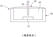
Fig. 1 shows a schematic diagram of a prior art LED.
Fig. 2 shows an LED package with silicone cover.
The present disclosure may take form in various components and arrangements of components, and in various process operations and arrangements of process operations. The present disclosure is illustrated in the figures, where like reference numerals may indicate corresponding or similar parts throughout the several views. The drawings are only for purposes of illustrating the preferred embodiments and are not to be construed as limiting the disclosure. The innovative features aspects of the present disclosure should become apparent to those of ordinary skill in the art upon consideration of the following description of the drawings.
Detailed Description
The following detailed description is merely exemplary in nature and is not intended to limit the application and uses of the disclosure. Furthermore, there is no intention to be bound by any theory presented in the preceding background or brief summary or the following detailed description. Although embodiments of the present technology are described herein primarily in connection with PFS LED packages and, in particular, Nichia 757 BSY-PFS LED packages, the concepts are also applicable to other types of phosphor-loaded LEDs and, in particular, other types of heavily phosphor-loaded LEDs. In particular, the concept is most applicable in LED packages where the weight ratio of phosphor to silicone is high (20% or higher), and at least one phosphor exhibits sensitivity to ambient atmospheric components such as moisture.
Fig. 1 shows an exemplary prior art LED package 10. The package 10 includes a Light Emitting Diode (LED) chip 12. A mixed phosphor and silicone layer 22 covers the chip 12. The LED chip 12 and the phosphor silicone hybrid layer 22 are sealed with a lens 18. The LED package 10 includes an outer encapsulant 30.
The hybrid phosphor silicone layer 22 is radiatively coupled to the LED chip 12 in the direction indicated by arrow 24. Radiatively coupled means that the elements are interrelated such that at least a portion of the radiation emitted from one is emitted to the other.
One embodiment of a heavily phosphor-loaded LED package 50 with greater stability is re-illustrated in fig. 2. The package 50 includes a semiconductor UV or visible radiation source, such as a Light Emitting Diode (LED) chip 52. A mixed phosphor and silicone layer 54 covers the chip 52.
The package 50 may include any semiconductor visible or UV light source capable of producing white light when its emitted radiation is directed onto a phosphor. The preferred peak emission of the LED chip 52 will depend on the isotropy of the phosphor used and may range from, for example, 250-550 nm. However, in one preferred embodiment, the emission of the LED will be in the violet to blue-green region and have a peak wavelength in the range from about 420 to about 500 nm. Then, generally, semiconductor light sources include LEDs doped with various impurities. Thus, an LED may comprise a semiconductor diode based on any suitable III-V, II-VI or IV-IV semiconductor layer and having a peak emission wavelength of about 250 to 550 nm.
Although the general discussion of the exemplary structures of the invention described herein refers to inorganic LED-based light sources, it should be understood that the LED chips may be replaced by organic light emitting structures or other radiation sources, unless otherwise indicated, and any reference to an LED chip or semiconductor is merely representative of any suitable radiation source.
The phosphor silicone hybrid layer 54 is desirably phosphor heavy-loaded with phosphor, especially 20% or more by weight phosphor. The phosphor silicone hybrid layer 54 is typically about 0.2 mm thick. In a preferred embodiment, the phosphor is a mixture of a PFS phosphor and a BSY phosphor or spectrally-similar phosphor. Particularly preferred are the Nichia Mint phosphor (BSY) and the GE PFS phosphor, which are desirable in low to medium power LED packages. An example is the Nichia 757 package.
A silicone overlayer 56 is provided on top of the phosphor silicone hybrid layer 54. The cover layer has a thickness of about 0.1 mm, desirably between about 0.1 and 0.5 mm. The silicone used is desirably the same type as in the phosphor silicone hybrid layer 54.
The silicone overlayer 56 is desirably applied from a mixture or synthetically produced immediately after dispensing of the silicone/phosphor slurry and subsequently cured simultaneously to avoid separation. In a preferred embodiment, the silicone protective overcoat 56 may be formed by gravity settling of the phosphor in the silicone mixture prior to curing the silicone phosphor mixture in the LED package. The settling process may be assisted by artificially creating additional gravity through a centrifuge or similar device. This gravitational action physically deposits the phosphor silicone mixture layer 54 down onto the LED chip 52 and allows the silicone to bleed to the top to form a silicone-only protective overcoat 56.
The LED chip 52 and the phosphor silicone hybrid layer 54 may be encapsulated with a lens 58. The lens 58 may be, for example, an epoxy, plastic, low temperature glass, polymer, thermoplastic, thermoset material, resin, or other type of LED encapsulant material known in the art. Optionally, the lens 58 is spin-on glass or some other material with a high index of refraction. In a preferred embodiment, the lens 58 is a polymeric material, such as an epoxy, silicone, or silicone epoxy, although other organic or inorganic encapsulants can be used.
The lens 58 is preferably transparent or substantially light transmissive with respect to the wavelength of light generated by the LED chip 52 and the phosphor silicone hybrid material 54. In an alternative embodiment, the package 50 may include only the encapsulant material without the outer lens.
The outer encapsulant 60 of the LED package is typically made of a polymer composite material EMC (epoxy moldable composite). The LED chip 52 may be supported, for example, by a lead frame (not shown), by a self-supporting electrode, the bottom of the encapsulant 60, or by a submount (not shown) mounted to the housing or lead frame. The LED chip 52 is electrically attached to electrical contacts at the bottom surface of the outer encapsulant 60. It is known to those skilled in the art that there may be multiple chips in an LED package with similar functional properties.
Due to its phosphor protection and isolation from environmental elements such as water, the silicone overlayer 56 has been quantified to provide a 25% improvement in package color shift compared to the same LED package without the silicone overlayer.
Examples of the invention
Nichia 757 LEDs were made with high BSY-PFS phosphor loading (49: 40:11 silicone: PFS: BSY weight percent) with or without silicone overlayer and compared under controlled operating conditions. The amount of phosphor used is the same in both cases and the LED drive and ambient conditions remain the same. The LED operating condition was 30 mA in a 47C constant temperature chamber.
Table 1 below shows the relative improvement in color shift.
TABLE 1

The improvement in color shift after 500 operating hours was 34%, and the improvement after 4000 operating hours was 29%.
Alternative embodiments, examples, and modifications that are still encompassed by the present disclosure may be made by those of skill in the art, particularly in light of the foregoing teachings. Furthermore, it is to be understood that the terminology used to describe the disclosure is intended to be in the nature of words of description rather than of limitation.
Those skilled in the art will also appreciate that various changes and modifications of the preferred and alternative embodiments described above can be configured without departing from the scope and spirit of the present disclosure. It is, therefore, to be understood that within the scope of the appended claims, the disclosure may be practiced other than as specifically described herein.
Claims (14)
1. A phosphor-loaded LED package, comprising:
LED;
a first layer comprising a mixture of phosphor and silicone covering the LED, wherein the mixture comprises at least 20% by weight phosphor to silicone and the mixture comprises at least K2[SiF6]:Mn4+(PFS) phosphor; and
a cover layer comprising silicone, wherein the cover layer has a thickness of about 0.1 mm or greater, the cover layer formed by gravity precipitation of phosphor in the mixture of phosphor and silicone, wherein the cover layer is made of the same silicone as in the mixture of the first layer.
2. The LED package of any of the preceding claims, wherein PFS phosphor in said mixture exhibits moisture sensitivity.
3. The LED package of any of the preceding claims, wherein the blend comprises a red phosphor and a yellow phosphor.
4. The LED package of any of the preceding claims, wherein the mixture comprises a YAG phosphor.
5. The LED package according to any of the preceding claims, wherein the LED package uses a BSY-PFS phosphor.
6. The LED package according to any of the preceding claims, wherein the LED package is a < 1W low to medium power LED package.
7. The LED package of any preceding claim, wherein the package has at least a 25% improvement in color shift compared to the same package without the cover layer.
8. A method, comprising:
applying a cover layer comprising silicone onto a first layer covering the LEDs;
wherein the first layer comprises a blend of phosphor and silicone covering the LED, wherein the blend comprises at least 20% by weight phosphor to silicone, and the blend comprises at least K2[SiF6]:Mn4+(PFS) phosphor, and
wherein the overlayer is formed by gravity precipitation of phosphor in the mixture of phosphor and silicone, wherein the overlayer has a thickness of about 0.1 mm or greater, wherein the overlayer is made of the same silicone as in the mixture of the first layer, wherein the silicone overlayer is formed by precipitation of phosphor in the phosphor silicone mixture prior to curing of the phosphor silicone mixture, providing the first layer and the silicone overlayer.
9. The method of claim 8, wherein the method improves the stability of heavily phosphor-filled LED packages.
10. The method of claim 8, wherein the mixture comprises PFS phosphor and BSY phosphor, or phosphors spectrally similar to PFS and BSY phosphors.
11. The method of claim 8, wherein the LED package is a low to medium power LED package using BSY-PFS phosphor.
12. The method of claim 8, wherein the package has at least a 25% color shift improvement compared to the same package without a silicone overlayer.
13. The method of claim 8, wherein the settling of the phosphor on the phosphor silicone blend is assisted by enhanced gravity.
14. The method of claim 8, wherein the capping layer does not include a phosphor.
Applications Claiming Priority (3)
| Application Number | Priority Date | Filing Date | Title |
|---|---|---|---|
| US14/217,831 US9680067B2 (en) | 2014-03-18 | 2014-03-18 | Heavily phosphor loaded LED packages having higher stability |
| US14/217831 | 2014-03-18 | ||
| CN201580014432.0A CN106463584A (en) | 2014-03-18 | 2015-02-23 | Heavily phosphor loaded led package |
Related Parent Applications (1)
| Application Number | Title | Priority Date | Filing Date |
|---|---|---|---|
| CN201580014432.0A Division CN106463584A (en) | 2014-03-18 | 2015-02-23 | Heavily phosphor loaded led package |
Publications (1)
| Publication Number | Publication Date |
|---|---|
| CN113675322A true CN113675322A (en) | 2021-11-19 |
Family
ID=52596638
Family Applications (2)
| Application Number | Title | Priority Date | Filing Date |
|---|---|---|---|
| CN201580014432.0A Pending CN106463584A (en) | 2014-03-18 | 2015-02-23 | Heavily phosphor loaded led package |
| CN202110725667.8A Pending CN113675322A (en) | 2014-03-18 | 2015-02-23 | Heavily phosphor-filled LED package |
Family Applications Before (1)
| Application Number | Title | Priority Date | Filing Date |
|---|---|---|---|
| CN201580014432.0A Pending CN106463584A (en) | 2014-03-18 | 2015-02-23 | Heavily phosphor loaded led package |
Country Status (10)
| Country | Link |
|---|---|
| US (1) | US9680067B2 (en) |
| EP (2) | EP3120394B1 (en) |
| JP (1) | JP6855245B2 (en) |
| KR (3) | KR20220045236A (en) |
| CN (2) | CN106463584A (en) |
| CA (1) | CA2942044C (en) |
| MX (1) | MX2016012013A (en) |
| MY (1) | MY178038A (en) |
| TW (1) | TWI657600B (en) |
| WO (1) | WO2015142478A1 (en) |
Families Citing this family (9)
| Publication number | Priority date | Publication date | Assignee | Title |
|---|---|---|---|---|
| US9680067B2 (en) | 2014-03-18 | 2017-06-13 | GE Lighting Solutions, LLC | Heavily phosphor loaded LED packages having higher stability |
| US9590148B2 (en) * | 2014-03-18 | 2017-03-07 | GE Lighting Solutions, LLC | Encapsulant modification in heavily phosphor loaded LED packages for improved stability |
| EP3590307B1 (en) | 2017-02-28 | 2023-09-27 | Quarkstar LLC | Lifetime color stabilization of color-shifting artificial light sources |
| RU2666578C1 (en) * | 2017-08-08 | 2018-09-11 | Акционерное общество "Центральный научно-исследовательский институт "Электрон" | Light-emitting diode |
| JP7002665B2 (en) * | 2018-02-12 | 2022-02-04 | シグニファイ ホールディング ビー ヴィ | LED light source with fluoride phosphor |
| US11056625B2 (en) * | 2018-02-19 | 2021-07-06 | Creeled, Inc. | Clear coating for light emitting device exterior having chemical resistance and related methods |
| CN109668062A (en) * | 2018-12-11 | 2019-04-23 | 业成科技(成都)有限公司 | Light-emitting diode area source structure |
| WO2021021984A1 (en) * | 2019-07-30 | 2021-02-04 | Current Lighting Solutions, Llc | Stable phosphor converted led and systems using the same |
| GB2590450B (en) * | 2019-12-18 | 2022-01-05 | Plessey Semiconductors Ltd | Light emitting diode precursor |
Citations (2)
| Publication number | Priority date | Publication date | Assignee | Title |
|---|---|---|---|---|
| CN101939857A (en) * | 2008-02-07 | 2011-01-05 | 三菱化学株式会社 | Semiconductor light emitting device, backlight, color image display device and phosphor to be used for them |
| CN103299440A (en) * | 2010-12-21 | 2013-09-11 | 奥斯兰姆奥普托半导体有限责任公司 | Method for producing an optoelectronic component, and optoelectronic component |
Family Cites Families (43)
| Publication number | Priority date | Publication date | Assignee | Title |
|---|---|---|---|---|
| TW383508B (en) * | 1996-07-29 | 2000-03-01 | Nichia Kagaku Kogyo Kk | Light emitting device and display |
| JP4271747B2 (en) | 1997-07-07 | 2009-06-03 | 株式会社朝日ラバー | Translucent coating material for light emitting diode and fluorescent color light source |
| US6204523B1 (en) | 1998-11-06 | 2001-03-20 | Lumileds Lighting, U.S., Llc | High stability optical encapsulation and packaging for light-emitting diodes in the green, blue, and near UV range |
| KR100923804B1 (en) | 2001-09-03 | 2009-10-27 | 파나소닉 주식회사 | Semiconductor light emitting device, light emitting apparatus and production method for semiconductor light emitting device |
| TWI245436B (en) | 2003-10-30 | 2005-12-11 | Kyocera Corp | Package for housing light-emitting element, light-emitting apparatus and illumination apparatus |
| US7497973B2 (en) * | 2005-02-02 | 2009-03-03 | Lumination Llc | Red line emitting phosphor materials for use in LED applications |
| TWI413274B (en) * | 2005-03-18 | 2013-10-21 | Mitsubishi Chem Corp | Light-emitting device, white light-emitting device, lighting device and image display device |
| JP2007123390A (en) * | 2005-10-26 | 2007-05-17 | Kyocera Corp | Light emitting device |
| US7521728B2 (en) | 2006-01-20 | 2009-04-21 | Cree, Inc. | Packages for semiconductor light emitting devices utilizing dispensed reflectors and methods of forming the same |
| KR100785492B1 (en) | 2006-04-17 | 2007-12-13 | 한국과학기술원 | Yellow emitting Ce??doped silicate phosphor and preparation method thereof, and white light emitting diodes comprising said Ce??doped silicate phosphor |
| JP5205724B2 (en) * | 2006-08-04 | 2013-06-05 | 日亜化学工業株式会社 | Light emitting device |
| JP5578597B2 (en) * | 2007-09-03 | 2014-08-27 | 独立行政法人物質・材料研究機構 | Phosphor, method for manufacturing the same, and light emitting device using the same |
| US9287469B2 (en) * | 2008-05-02 | 2016-03-15 | Cree, Inc. | Encapsulation for phosphor-converted white light emitting diode |
| JP2010093132A (en) | 2008-10-09 | 2010-04-22 | Sharp Corp | Semiconductor light emitting device, and image display and liquid crystal display using the same |
| JP5308773B2 (en) | 2008-10-30 | 2013-10-09 | スタンレー電気株式会社 | Semiconductor light emitting device |
| US8039862B2 (en) | 2009-03-10 | 2011-10-18 | Nepes Led Corporation | White light emitting diode package having enhanced white lighting efficiency and method of making the same |
| US8058667B2 (en) | 2009-03-10 | 2011-11-15 | Nepes Led Corporation | Leadframe package for light emitting diode device |
| JP5423120B2 (en) | 2009-04-17 | 2014-02-19 | 三菱化学株式会社 | Semiconductor light emitting device |
| JP2011054958A (en) * | 2009-08-06 | 2011-03-17 | Mitsubishi Chemicals Corp | Semiconductor light emitting device, image display device, and lighting system |
| US20110031516A1 (en) | 2009-08-07 | 2011-02-10 | Koninklijke Philips Electronics N.V. | Led with silicone layer and laminated remote phosphor layer |
| US20100276712A1 (en) * | 2009-11-03 | 2010-11-04 | Alexander Shaikevitch | Light emitting diode with thin multilayer phosphor film |
| JP5076017B2 (en) * | 2010-08-23 | 2012-11-21 | 株式会社東芝 | Light emitting device |
| WO2012029695A1 (en) * | 2010-08-31 | 2012-03-08 | 日亜化学工業株式会社 | Light emitting device and method for manufacturing same |
| JP5622494B2 (en) | 2010-09-09 | 2014-11-12 | スタンレー電気株式会社 | Light emitting device and manufacturing method thereof |
| EP2629341B8 (en) | 2010-10-15 | 2020-04-08 | Mitsubishi Chemical Corporation | White light emitting device and lighting device |
| US9085728B2 (en) * | 2011-01-28 | 2015-07-21 | Showa Denko K.K. | Composition containing quantum dot fluorescent body, molded body of quantum dot fluorescent body dispersion resin, structure containing quantum dot fluorescent body, light-emitting device, electronic apparatus, mechanical device, and method for producing molded body of quantum dot fluorescent body dispersion resin |
| DE102011003969B4 (en) | 2011-02-11 | 2023-03-09 | OSRAM Opto Semiconductors Gesellschaft mit beschränkter Haftung | Process for producing an optoelectronic component |
| JP5762044B2 (en) * | 2011-02-23 | 2015-08-12 | 三菱電機株式会社 | Light emitting device, light emitting device group, and manufacturing method |
| US8252613B1 (en) | 2011-03-23 | 2012-08-28 | General Electric Company | Color stable manganese-doped phosphors |
| TWI489656B (en) | 2011-03-25 | 2015-06-21 | Samsung Electronics Co Ltd | Light emitting diode, manufacturing method thereof, light emitting diode module, and manufacturing method thereof |
| JP5105132B1 (en) * | 2011-06-02 | 2012-12-19 | 三菱化学株式会社 | Semiconductor light emitting device, semiconductor light emitting system, and lighting fixture |
| EP3346512B1 (en) | 2011-06-03 | 2023-06-07 | Citizen Electronics Co., Ltd. | Semiconductor light-emitting device, exhibit-irradiating illumination device, meat-irradiating illumination device, vegetable-irradiating illumination device, fresh fish-irradiating illumination device, general-purpose illumination device, and semiconductor light-emitting system |
| JP5919504B2 (en) * | 2011-06-30 | 2016-05-18 | パナソニックIpマネジメント株式会社 | Light emitting device |
| DE102011081083A1 (en) | 2011-08-17 | 2013-02-21 | Osram Ag | PRESS TOOL AND METHOD FOR PRESSING A SILICONE ELEMENT |
| US8841689B2 (en) * | 2012-02-03 | 2014-09-23 | Shin-Etsu Chemical Co., Ltd. | Heat-curable silicone resin sheet having phosphor-containing layer and phosphor-free layer, method of producing light emitting device utilizing same and light emitting semiconductor device obtained by the method |
| US9343441B2 (en) * | 2012-02-13 | 2016-05-17 | Cree, Inc. | Light emitter devices having improved light output and related methods |
| JP5840540B2 (en) * | 2012-03-15 | 2016-01-06 | 株式会社東芝 | White lighting equipment |
| DE102012208900A1 (en) | 2012-05-25 | 2013-11-28 | Osram Opto Semiconductors Gmbh | Method for producing optoelectronic components and apparatus for producing optoelectronic components |
| US10424702B2 (en) | 2012-06-11 | 2019-09-24 | Cree, Inc. | Compact LED package with reflectivity layer |
| JP2014041993A (en) * | 2012-07-24 | 2014-03-06 | Toyoda Gosei Co Ltd | Light-emitting device and method of manufacturing the same |
| DE102012213195A1 (en) | 2012-07-26 | 2014-01-30 | Osram Gmbh | Method for covering a surface with phosphor |
| US9761763B2 (en) * | 2012-12-21 | 2017-09-12 | Soraa, Inc. | Dense-luminescent-materials-coated violet LEDs |
| US9680067B2 (en) | 2014-03-18 | 2017-06-13 | GE Lighting Solutions, LLC | Heavily phosphor loaded LED packages having higher stability |
-
2014
- 2014-03-18 US US14/217,831 patent/US9680067B2/en active Active
-
2015
- 2015-02-23 CN CN201580014432.0A patent/CN106463584A/en active Pending
- 2015-02-23 WO PCT/US2015/017010 patent/WO2015142478A1/en active Application Filing
- 2015-02-23 CN CN202110725667.8A patent/CN113675322A/en active Pending
- 2015-02-23 KR KR1020227009789A patent/KR20220045236A/en not_active IP Right Cessation
- 2015-02-23 MY MYPI2016702904A patent/MY178038A/en unknown
- 2015-02-23 KR KR1020167028521A patent/KR20160133528A/en not_active Application Discontinuation
- 2015-02-23 EP EP15707243.0A patent/EP3120394B1/en active Active
- 2015-02-23 KR KR1020247004203A patent/KR20240023202A/en active Application Filing
- 2015-02-23 EP EP23216627.2A patent/EP4332196A3/en active Pending
- 2015-02-23 JP JP2016556865A patent/JP6855245B2/en active Active
- 2015-02-23 CA CA2942044A patent/CA2942044C/en active Active
- 2015-02-23 MX MX2016012013A patent/MX2016012013A/en unknown
- 2015-03-05 TW TW104107021A patent/TWI657600B/en active
Patent Citations (2)
| Publication number | Priority date | Publication date | Assignee | Title |
|---|---|---|---|---|
| CN101939857A (en) * | 2008-02-07 | 2011-01-05 | 三菱化学株式会社 | Semiconductor light emitting device, backlight, color image display device and phosphor to be used for them |
| CN103299440A (en) * | 2010-12-21 | 2013-09-11 | 奥斯兰姆奥普托半导体有限责任公司 | Method for producing an optoelectronic component, and optoelectronic component |
Also Published As
| Publication number | Publication date |
|---|---|
| WO2015142478A1 (en) | 2015-09-24 |
| EP3120394A1 (en) | 2017-01-25 |
| MX2016012013A (en) | 2016-12-05 |
| JP2017511599A (en) | 2017-04-20 |
| TWI657600B (en) | 2019-04-21 |
| CN106463584A (en) | 2017-02-22 |
| EP3120394B1 (en) | 2023-12-20 |
| KR20220045236A (en) | 2022-04-12 |
| KR20160133528A (en) | 2016-11-22 |
| CA2942044A1 (en) | 2015-09-24 |
| US20150270451A1 (en) | 2015-09-24 |
| EP4332196A3 (en) | 2024-06-05 |
| MY178038A (en) | 2020-09-30 |
| CA2942044C (en) | 2023-01-03 |
| KR20240023202A (en) | 2024-02-20 |
| JP6855245B2 (en) | 2021-04-07 |
| US9680067B2 (en) | 2017-06-13 |
| TW201547060A (en) | 2015-12-16 |
| EP4332196A2 (en) | 2024-03-06 |
Similar Documents
| Publication | Publication Date | Title |
|---|---|---|
| US9680067B2 (en) | Heavily phosphor loaded LED packages having higher stability | |
| US10862009B2 (en) | Encapsulant modification in heavily phosphor loaded LED packages for improved stability | |
| US8476655B2 (en) | Electromagnetic-radiation-emitting optoelectronic component and method for producing an optoelectronic component | |
| CN101996986A (en) | White light-emitting diode packages with tunable colour temperature | |
| TWI625380B (en) | Phosphor assembly for light emitting devices | |
| US7965028B2 (en) | White light emitting device and producing method thereof | |
| JP5905648B2 (en) | Light emitting device using semiconductor | |
| EP2770546A2 (en) | Light emitting module and lighting device | |
| KR102514150B1 (en) | Light emitting device and lighting unit having thereof | |
| KR102401589B1 (en) | High CRI White Light Emitting Device with Spectrum Beneficial to Human | |
| JP2008227550A (en) | Light emitting diode, its production method, and white lighting apparatus | |
| KR20190081679A (en) | Color conversion material and led package using the same | |
| KR20060088228A (en) | Light apparatus capable of emitting light of multiple wavelengths using nanometer fluorescent material, light device and manufacturing method thereof |
Legal Events
| Date | Code | Title | Description |
|---|---|---|---|
| PB01 | Publication | ||
| PB01 | Publication | ||
| SE01 | Entry into force of request for substantive examination | ||
| SE01 | Entry into force of request for substantive examination |