CN112903639B - Integrated device with external light source for detection, detection and analysis of molecules - Google Patents
Integrated device with external light source for detection, detection and analysis of molecules Download PDFInfo
- Publication number
- CN112903639B CN112903639B CN202110063547.6A CN202110063547A CN112903639B CN 112903639 B CN112903639 B CN 112903639B CN 202110063547 A CN202110063547 A CN 202110063547A CN 112903639 B CN112903639 B CN 112903639B
- Authority
- CN
- China
- Prior art keywords
- sample
- sample well
- waveguide
- excitation
- integrated device
- Prior art date
- Legal status (The legal status is an assumption and is not a legal conclusion. Google has not performed a legal analysis and makes no representation as to the accuracy of the status listed.)
- Active
Links
Images


Classifications
-
- G—PHYSICS
- G01—MEASURING; TESTING
- G01N—INVESTIGATING OR ANALYSING MATERIALS BY DETERMINING THEIR CHEMICAL OR PHYSICAL PROPERTIES
- G01N21/00—Investigating or analysing materials by the use of optical means, i.e. using sub-millimetre waves, infrared, visible or ultraviolet light
- G01N21/62—Systems in which the material investigated is excited whereby it emits light or causes a change in wavelength of the incident light
- G01N21/63—Systems in which the material investigated is excited whereby it emits light or causes a change in wavelength of the incident light optically excited
- G01N21/64—Fluorescence; Phosphorescence
- G01N21/6408—Fluorescence; Phosphorescence with measurement of decay time, time resolved fluorescence
-
- C—CHEMISTRY; METALLURGY
- C12—BIOCHEMISTRY; BEER; SPIRITS; WINE; VINEGAR; MICROBIOLOGY; ENZYMOLOGY; MUTATION OR GENETIC ENGINEERING
- C12Q—MEASURING OR TESTING PROCESSES INVOLVING ENZYMES, NUCLEIC ACIDS OR MICROORGANISMS; COMPOSITIONS OR TEST PAPERS THEREFOR; PROCESSES OF PREPARING SUCH COMPOSITIONS; CONDITION-RESPONSIVE CONTROL IN MICROBIOLOGICAL OR ENZYMOLOGICAL PROCESSES
- C12Q1/00—Measuring or testing processes involving enzymes, nucleic acids or microorganisms; Compositions therefor; Processes of preparing such compositions
- C12Q1/68—Measuring or testing processes involving enzymes, nucleic acids or microorganisms; Compositions therefor; Processes of preparing such compositions involving nucleic acids
- C12Q1/6869—Methods for sequencing
- C12Q1/6874—Methods for sequencing involving nucleic acid arrays, e.g. sequencing by hybridisation
-
- G—PHYSICS
- G01—MEASURING; TESTING
- G01N—INVESTIGATING OR ANALYSING MATERIALS BY DETERMINING THEIR CHEMICAL OR PHYSICAL PROPERTIES
- G01N21/00—Investigating or analysing materials by the use of optical means, i.e. using sub-millimetre waves, infrared, visible or ultraviolet light
- G01N21/62—Systems in which the material investigated is excited whereby it emits light or causes a change in wavelength of the incident light
- G01N21/63—Systems in which the material investigated is excited whereby it emits light or causes a change in wavelength of the incident light optically excited
- G01N21/64—Fluorescence; Phosphorescence
- G01N21/6428—Measuring fluorescence of fluorescent products of reactions or of fluorochrome labelled reactive substances, e.g. measuring quenching effects, using measuring "optrodes"
-
- G—PHYSICS
- G01—MEASURING; TESTING
- G01N—INVESTIGATING OR ANALYSING MATERIALS BY DETERMINING THEIR CHEMICAL OR PHYSICAL PROPERTIES
- G01N21/00—Investigating or analysing materials by the use of optical means, i.e. using sub-millimetre waves, infrared, visible or ultraviolet light
- G01N21/62—Systems in which the material investigated is excited whereby it emits light or causes a change in wavelength of the incident light
- G01N21/63—Systems in which the material investigated is excited whereby it emits light or causes a change in wavelength of the incident light optically excited
- G01N21/64—Fluorescence; Phosphorescence
- G01N21/645—Specially adapted constructive features of fluorimeters
- G01N21/6452—Individual samples arranged in a regular 2D-array, e.g. multiwell plates
- G01N21/6454—Individual samples arranged in a regular 2D-array, e.g. multiwell plates using an integrated detector array
-
- G—PHYSICS
- G01—MEASURING; TESTING
- G01N—INVESTIGATING OR ANALYSING MATERIALS BY DETERMINING THEIR CHEMICAL OR PHYSICAL PROPERTIES
- G01N21/00—Investigating or analysing materials by the use of optical means, i.e. using sub-millimetre waves, infrared, visible or ultraviolet light
- G01N21/62—Systems in which the material investigated is excited whereby it emits light or causes a change in wavelength of the incident light
- G01N21/63—Systems in which the material investigated is excited whereby it emits light or causes a change in wavelength of the incident light optically excited
- G01N21/64—Fluorescence; Phosphorescence
- G01N21/645—Specially adapted constructive features of fluorimeters
- G01N21/6456—Spatial resolved fluorescence measurements; Imaging
-
- G—PHYSICS
- G01—MEASURING; TESTING
- G01N—INVESTIGATING OR ANALYSING MATERIALS BY DETERMINING THEIR CHEMICAL OR PHYSICAL PROPERTIES
- G01N21/00—Investigating or analysing materials by the use of optical means, i.e. using sub-millimetre waves, infrared, visible or ultraviolet light
- G01N21/62—Systems in which the material investigated is excited whereby it emits light or causes a change in wavelength of the incident light
- G01N21/63—Systems in which the material investigated is excited whereby it emits light or causes a change in wavelength of the incident light optically excited
- G01N21/64—Fluorescence; Phosphorescence
- G01N21/645—Specially adapted constructive features of fluorimeters
- G01N21/648—Specially adapted constructive features of fluorimeters using evanescent coupling or surface plasmon coupling for the excitation of fluorescence
-
- G—PHYSICS
- G01—MEASURING; TESTING
- G01N—INVESTIGATING OR ANALYSING MATERIALS BY DETERMINING THEIR CHEMICAL OR PHYSICAL PROPERTIES
- G01N21/00—Investigating or analysing materials by the use of optical means, i.e. using sub-millimetre waves, infrared, visible or ultraviolet light
- G01N21/62—Systems in which the material investigated is excited whereby it emits light or causes a change in wavelength of the incident light
- G01N21/63—Systems in which the material investigated is excited whereby it emits light or causes a change in wavelength of the incident light optically excited
- G01N21/64—Fluorescence; Phosphorescence
- G01N21/6486—Measuring fluorescence of biological material, e.g. DNA, RNA, cells
-
- G—PHYSICS
- G01—MEASURING; TESTING
- G01N—INVESTIGATING OR ANALYSING MATERIALS BY DETERMINING THEIR CHEMICAL OR PHYSICAL PROPERTIES
- G01N21/00—Investigating or analysing materials by the use of optical means, i.e. using sub-millimetre waves, infrared, visible or ultraviolet light
- G01N21/62—Systems in which the material investigated is excited whereby it emits light or causes a change in wavelength of the incident light
- G01N21/63—Systems in which the material investigated is excited whereby it emits light or causes a change in wavelength of the incident light optically excited
- G01N21/64—Fluorescence; Phosphorescence
- G01N2021/6417—Spectrofluorimetric devices
- G01N2021/6419—Excitation at two or more wavelengths
-
- G—PHYSICS
- G01—MEASURING; TESTING
- G01N—INVESTIGATING OR ANALYSING MATERIALS BY DETERMINING THEIR CHEMICAL OR PHYSICAL PROPERTIES
- G01N21/00—Investigating or analysing materials by the use of optical means, i.e. using sub-millimetre waves, infrared, visible or ultraviolet light
- G01N21/62—Systems in which the material investigated is excited whereby it emits light or causes a change in wavelength of the incident light
- G01N21/63—Systems in which the material investigated is excited whereby it emits light or causes a change in wavelength of the incident light optically excited
- G01N21/64—Fluorescence; Phosphorescence
- G01N2021/6417—Spectrofluorimetric devices
- G01N2021/6421—Measuring at two or more wavelengths
-
- G—PHYSICS
- G01—MEASURING; TESTING
- G01N—INVESTIGATING OR ANALYSING MATERIALS BY DETERMINING THEIR CHEMICAL OR PHYSICAL PROPERTIES
- G01N21/00—Investigating or analysing materials by the use of optical means, i.e. using sub-millimetre waves, infrared, visible or ultraviolet light
- G01N21/62—Systems in which the material investigated is excited whereby it emits light or causes a change in wavelength of the incident light
- G01N21/63—Systems in which the material investigated is excited whereby it emits light or causes a change in wavelength of the incident light optically excited
- G01N21/64—Fluorescence; Phosphorescence
- G01N21/6428—Measuring fluorescence of fluorescent products of reactions or of fluorochrome labelled reactive substances, e.g. measuring quenching effects, using measuring "optrodes"
- G01N2021/6439—Measuring fluorescence of fluorescent products of reactions or of fluorochrome labelled reactive substances, e.g. measuring quenching effects, using measuring "optrodes" with indicators, stains, dyes, tags, labels, marks
- G01N2021/6441—Measuring fluorescence of fluorescent products of reactions or of fluorochrome labelled reactive substances, e.g. measuring quenching effects, using measuring "optrodes" with indicators, stains, dyes, tags, labels, marks with two or more labels
-
- G—PHYSICS
- G01—MEASURING; TESTING
- G01N—INVESTIGATING OR ANALYSING MATERIALS BY DETERMINING THEIR CHEMICAL OR PHYSICAL PROPERTIES
- G01N21/00—Investigating or analysing materials by the use of optical means, i.e. using sub-millimetre waves, infrared, visible or ultraviolet light
- G01N21/62—Systems in which the material investigated is excited whereby it emits light or causes a change in wavelength of the incident light
- G01N21/63—Systems in which the material investigated is excited whereby it emits light or causes a change in wavelength of the incident light optically excited
- G01N21/64—Fluorescence; Phosphorescence
- G01N21/645—Specially adapted constructive features of fluorimeters
- G01N2021/6463—Optics
- G01N2021/6471—Special filters, filter wheel
-
- G—PHYSICS
- G01—MEASURING; TESTING
- G01N—INVESTIGATING OR ANALYSING MATERIALS BY DETERMINING THEIR CHEMICAL OR PHYSICAL PROPERTIES
- G01N2201/00—Features of devices classified in G01N21/00
- G01N2201/06—Illumination; Optics
- G01N2201/064—Stray light conditioning
-
- G—PHYSICS
- G01—MEASURING; TESTING
- G01N—INVESTIGATING OR ANALYSING MATERIALS BY DETERMINING THEIR CHEMICAL OR PHYSICAL PROPERTIES
- G01N2201/00—Features of devices classified in G01N21/00
- G01N2201/06—Illumination; Optics
- G01N2201/069—Supply of sources
- G01N2201/0696—Pulsed
-
- G—PHYSICS
- G01—MEASURING; TESTING
- G01N—INVESTIGATING OR ANALYSING MATERIALS BY DETERMINING THEIR CHEMICAL OR PHYSICAL PROPERTIES
- G01N2201/00—Features of devices classified in G01N21/00
- G01N2201/08—Optical fibres; light guides
-
- G—PHYSICS
- G01—MEASURING; TESTING
- G01N—INVESTIGATING OR ANALYSING MATERIALS BY DETERMINING THEIR CHEMICAL OR PHYSICAL PROPERTIES
- G01N2201/00—Features of devices classified in G01N21/00
- G01N2201/12—Circuits of general importance; Signal processing
Abstract
The present invention relates to a system and method for analyzing single molecules and performing nucleic acid sequencing. The integrated device includes a plurality of pixels having sample wells configured to receive a sample that emits radiation when excited. The integrated device includes at least one waveguide configured to propagate excitation energy to the sample well from a region of the integrated device for coupling with an excitation energy source. A pixel may also include at least one element for directing emitted energy towards a sensor within the pixel. The system also includes an instrument coupled to the integrated device. The apparatus may comprise an excitation energy source for providing excitation energy to the integrated device via an excitation energy coupling region coupled to the integrated device. The sample may be labeled with one of a plurality of markers that are distinguishable by a temporal parameter of the emitted energy, and the configuration of the sensor within one pixel may allow detection of the temporal parameter associated with the marker labeling the sample.
Description
The present application is a divisional application of the invention patent application having the name "integrated device with external light source for detecting, detecting and analyzing molecules" filed on 8/7/2015 for application No. 201580054785.3 (corresponding to PCT international application No. PCT/US 2015/044379) in china.
RELATED APPLICATIONS
This application claims priority from U.S. provisional patent application 62/035,258 entitled "integrated apparatus with external light source for detecting, detecting and analyzing molecules" filed on 8/2014 and U.S. provisional patent application 62/164,464 entitled "integrated apparatus with external light source for detecting, detecting and analyzing molecules" filed on 5/20/2015, each of which is incorporated herein by reference in its entirety.
This application is related to the following U.S. patent applications:
us provisional patent application 62/164,506 entitled "integrated device for temporal partitioning of received photons" filed on 20/5/2015;
U.S. provisional patent application No. 62/164,485 entitled "pulsed laser" filed on 20/5/2015;
U.S. provisional patent application 62/164,482 entitled "method for nucleic acid sequencing" filed 5/20/2015;
U.S. provisional patent application 62/035,242 entitled "optical systems and detection chips for detecting, and analyzing molecules" filed 8/2014, the entire contents of which are incorporated herein by reference;
United states non-provisional patent application entitled "integrated device for time-dividing received photons", filed on even date herewith under reference number R0708.70002US02;
U.S. non-provisional patent application entitled "optical systems and detection chips for detection, detection and analysis of molecules", filed on even date herewith under reference number R0708.70003US01.
The entire contents of each of the related applications listed above are incorporated herein by reference.
Technical Field
The present application relates generally to devices, methods and techniques for performing rapid, massively parallel quantitative analysis of biological and/or chemical samples, and methods of making the same.
Background
Detection and analysis of biological samples can be performed using biological assays ("bioassays"). Biometrics often involve large and expensive laboratory equipment, which requires training of an assistant researcher to operate the equipment and perform the biometrics. Furthermore, bioassays are usually performed in bulk, so that a large number of samples of a particular type are necessary for detection and quantification.
Some bioassays are performed by tagging samples with fluorescent labels that emit light at a specific wavelength. The labels are illuminated with a light source to cause luminescence, and the luminescence is detected with a photodetector to quantify the amount of luminescence emitted by the labels. Bioassays using fluorescent labels typically involve expensive laser light sources for illuminating the sample, complex bulky detection optics, and electronics to collect the luminescence from the illuminated sample.
Disclosure of Invention
The technology described herein relates to devices and methods for rapidly analyzing a specimen with an active pixel integration device that can interact with a mobile computing instrument. The integrated device may take the form of a single-use or reusable lab-on-a-chip or packaged module configured to receive a small sample and perform a large number of analyses on samples within the sample in parallel. The integrated device may be used in some embodiments to detect the presence of a particular chemical or biological analyte, in some embodiments to assess a chemical or biological response, and in some embodiments to determine a gene sequence. According to some embodiments, the integrated device may be used for single molecule gene sequencing.
According to some embodiments, the user places the sample in one of the chambers on the integrated device and inserts the integrated device into the receiving instrument. The receiving instrument interacts with the integration device, either alone or automatically in connection with a computer, receives data from the integration device, processes the received data, and provides the results of the analysis to the user. As can be appreciated, integrating and computing intelligence on a chip, accepting instruments, and/or computers reduces the level of skill required to be possessed by a user.
According to some embodiments of the present application, there is provided an integrated device including a plurality of pixels. One of the plurality of pixels includes: a sample well for receiving excitation energy from an excitation source external to the integrated device, and at least one sensor for receiving luminescence from a sample located in the sample well and generating a signal providing sample discrimination information based on the received luminescence.
In some embodiments, the signal is an indicator of a time parameter of the received luminescence. In some embodiments, the time parameter is a lifetime associated with luminescence from the sample. In some embodiments, the signal is an indicator of a luminescence spectrum. In some embodiments, the signal is an indicator of a characteristic wavelength of the luminescence. In some embodiments, the signal and excitation energy are indicative of an absorption spectrum of the sample. In some embodiments, the signal and excitation energy are indicative of a characteristic wavelength absorbed by the sample.
According to some embodiments of the present application, there is provided an integrated device including a pixel region including a plurality of pixels. One of the plurality of pixels has: a sample well on a surface of the integrated device, wherein the sample well is configured to receive a sample; at least one sensor for receiving luminescence from the sample well; and at least one waveguide for conveying excitation energy to the vicinity of the sample well. The integrated device includes an excitation source coupling region including coupling means for receiving excitation energy from an external excitation energy source and coupling the excitation energy into the waveguide.
According to some embodiments of the present application, there is provided a system comprising an excitation source module comprising an excitation source and an integrated device for emitting a pulse having an excitation energy of a first time period. The integrated device includes: a sample well for receiving a sample that emits luminescence when coupled to a pulse of excitation energy; a sensor that detects the light emission during a second period of time, wherein the second period of time occurs after the first period of time; a first energy path along which the pulse of excitation energy moves from the excitation source to the energy source coupling component; a second energy path along which the pulse of excitation energy moves from the energy source coupling means to the sample well; and a third energy path along which luminescence moves from the sample well to the sensor.
According to some embodiments of the present application, there is provided a method of detecting the presence of a molecule in a sample. The method includes introducing a sample labeled with one of a plurality of luminescent markers into a sample well, wherein at least a portion of the plurality of luminescent markers have different luminescent lifetime values. The method further comprises the following steps: irradiating the sample well with a pulse of light, measuring the arrival time of photons emitted from the sample well, and determining a characteristic of the marker based on the arrival time of the photons.
According to some embodiments of the present application, there is provided an integrated device comprising a sample well and a sensor. The sample well is for receiving a sample labeled with a plurality of luminescent markers, each luminescent marker of the plurality of luminescent markers having a different luminescent lifetime value. The sensor is for detecting light emission from one of the plurality of light emitting markers in a plurality of time periods, wherein the plurality of time periods are selected to distinguish among the plurality of light emitting markers.
According to some embodiments of the present application, there is provided an integrated device comprising a sample well and a plurality of sensors. The sample well is for receiving a sample labeled with one of the plurality of luminescent markers. Each of the plurality of light emitting markers emits luminescence in one of the plurality of spectral ranges, and a portion of the plurality of light emitting markers that emit luminescence in one of the plurality of spectral ranges each have a different luminescence lifetime value. Each sensor of the plurality of sensors is for detecting one spectral range of the plurality of spectral ranges in a plurality of time periods, and the plurality of time periods are selected to distinguish between a portion of the plurality of lighted signs.
According to some embodiments, a system is provided that includes a plurality of excitation sources and an integrated device. The plurality of excitation sources is for emitting a plurality of excitation energies, wherein each excitation source of the plurality of excitation sources emits a pulse of excitation energy of the plurality of excitation energies. The integrated device includes a sample well for receiving a sample labeled with one of a plurality of luminescent tags. Some of the plurality of luminescent markers luminesce upon illumination by one of a plurality of excitation energies each having a different lifetime value. The integrated device further includes a sensor for detecting luminescence from one of the plurality of luminescent markers in a plurality of time periods after the pulse of the one of the plurality of excitation energies, wherein the timing of the pulse of the one of the plurality of excitation energies and the plurality of time periods distinguish among the plurality of luminescent markers.
According to some embodiments of the present application, a method of forming an integrated device is provided. The method includes forming a plurality of sensor regions, wherein a sensor region of the plurality of sensor regions includes a plurality of sensors, thereby forming a plurality of sample wells, wherein a sample well of the plurality of sample wells is aligned with a corresponding sensor region of the plurality of sensor regions, and forming at least one waveguide for coupling excitation energy separate from the plurality of sample wells and directing the excitation energy to the at least one sample well.
According to some embodiments of the present application, there is provided an apparatus. The instrument includes: the integrated device includes at least one excitation source for providing at least one excitation energy, an excitation source positioning system for aligning the at least one excitation energy emitted by the at least one excitation source with a coupling region of the integrated device, and readout circuitry for receiving at least one readout signal representative of emission energy detected by a sensor on the integrated device.
According to some embodiments of the present application, a method of sequencing a target nucleic acid molecule is provided. The method includes providing an integrated device that includes a sample well that houses a target nucleic acid molecule, a polymerase, and a plurality of types of nucleotides or nucleotide analogs. Each of the plurality of types of nucleotides or nucleotide analogs is labeled with one or more labels. The method further comprises performing an extension reaction at a priming location of the target nucleic acid molecule in the presence of a polymerase, thereby sequentially incorporating at least a portion of the nucleotides or nucleotide analogs into a growing strand that is complementary to the target nucleic acid molecule, wherein the labeling of the nucleotides or nucleotide analogs incorporated into the growing strand with a label when excited with excitation energy produces emissions from the sample well and the emission lifetimes are distinguishable for multiple types of nucleotides or nucleotide analogs. The method further includes identifying a nucleotide or nucleotide analog based on the signal received from the sensor that is an indicator of emission lifetime, thereby sequencing the target nucleic acid molecule.
According to some embodiments of the present application, there is provided a method for nucleic acid sequencing. The method includes providing an integrated device comprising a plurality of sample wells and an excitation energy source operably coupled to the plurality of sample wells. Individual sample wells of the plurality of sample wells contain a target nucleic acid molecule, a polymerase, and a nucleotide or nucleotide analog. One tag of the plurality of tags labels each nucleotide or nucleotide analog. The method further comprises the following steps: the target nucleic acid molecule is subjected to a polymerization reaction in the presence of the nucleotide or nucleotide analog and a polymerase, thereby obtaining a growing strand that is complementary to the target nucleic acid molecule. In the case of incorporating nucleotides or nucleotide analogs into a growing strand, the plurality of labels emit emission light when excited by excitation energy from an excitation source. The method further comprises the following steps: detecting a lifetime of luminescence while performing an extension reaction, wherein the luminescence lifetime is distinguishable with respect to a plurality of markers; and identifying the sequence of the target nucleic acid molecule based on the luminescence lifetime.
According to some embodiments of the present application, a method of analyzing a sample is provided. The method comprises the following steps: depositing a sample on a surface of an integrated device having a plurality of pixels, wherein each pixel has a sample well for receiving a sample labeled with a first label of the plurality of labels and a sensor region having at least one sensor; aligning the integrated device with an instrument having at least one excitation energy source for coupling excitation energy to the sample well of the first pixel and readout circuitry for receiving readout signals from at least one sensor of the sensor region of the first pixel; illuminating the first marker with excitation energy; and detecting a lifetime of emission energy resulting from the emission of the first mark based on a readout signal from at least one sensor of the sensor area of the first pixel.
The term "pixel" as used in this disclosure may refer to one unit volume of an integrated device. The unit cell may include a sample well and a sensor. The unit cell may further include at least one excitation coupling optical structure (which may be referred to as a "first structure") for enhancing coupling of excitation energy from the excitation source to the sample well. The unit cell may further comprise at least one emission coupling structure for enhancing coupling of emission from the sample well to the sensor. The cell body may also include integrated electronic devices (e.g., CMOS devices). There may be a plurality of pixels arranged in an array on an integrated device.
The term "optical" as used in this disclosure may refer to the visible, near infrared, and short wavelength infrared bands.
The term "tag" as used in the present disclosure may refer to a tag, probe, or reporter (reporter), and includes a label attached to a sample to be analyzed, or to a reagent that can bind to the sample.
The phrase "excitation energy" as used in this disclosure may refer to any form of energy (e.g., radiative or non-radiative) delivered to the sample and/or the marker inside the sample well. The excitation energy of the radiation may comprise optical radiation at one or more characteristic wavelengths.
The phrase "characteristic wavelength" as used in this disclosure may refer to a center wavelength or dominant wavelength within a limited bandwidth of radiation. In some cases, a "characteristic wavelength" may refer to a peak wavelength of the radiation bandwidth. Examples of characteristic wavelengths of fluorophores are 563nm, 595nm, 662nm, and 687 nm.
The phrase "characteristic energy" as used in this disclosure may refer to energy associated with a characteristic wavelength.
The term "emission" as used in this disclosure may refer to emission from a tag and/or sample. This may include radiative emission (e.g., light emission) or non-radiative energy transfer (e.g., Dexter energy transfer or Resonant energy transfer). The emission is caused by excitation of the sample and/or the marker inside the sample well.
The phrase "emission from the sample well" or "emission from the sample" as used in this disclosure may refer to emission from the marker and/or the sample inside the sample well.
The term "self-aligned" as used in this disclosure may refer to a micromachining process in which at least two different elements (e.g., a sample well and an emission coupling structure, a sample well and an excitation source) may be fabricated and aligned to each other without employing two separate lithographic patterning steps, where a first lithographic patterning step (e.g., photolithography, ion beam lithography, EUV lithography) prints a pattern of a first element and a second lithographic patterning step is consistent with the first lithographic patterning step and prints a pattern of a second element. The self-aligned process may comprise including the pattern of both the first and second elements in a single lithographic patterning step, or may comprise forming the second element using features of the fabricated structure of the first element.
The term "sensor" as used in this disclosure may refer to one or more integrated circuit devices for sensing emissions from a sample well and producing at least one electrical signal that is representative of the sensed emissions.
The term "nanoscale" as used in this disclosure may refer to structures having at least one dimension or minimum feature size below about 150 nanometers (nm) but no greater than about 500 nm.
The term "microscale" as used in this disclosure may refer to structures having at least one dimension or minimum feature size between about 500nm and about 100 micrometers.
The phrase "enhancing excitation energy" as used in this disclosure may refer to increasing the intensity of excitation energy at the excitation region of the sample well. The intensity may be increased, for example, by concentrating and/or resonating the excitation energy incident on the sample well. In some cases, the intensity may be increased by an anti-reflective coating or lossy layer that allows further penetration of excitation energy into the excitation region of the sample well. The enhancement of excitation energy may be a comparative reference to embodiments that do not include structures for enhancing excitation energy in the excitation region of the sample well.
The terms "about," "approximately," and "approximately" as used in this disclosure may refer to a value and are intended to include both the recited value plus and minus an acceptable variation. In some embodiments, the amount of deterioration may be less than 5%, in some embodiments less than 10%, in some embodiments less than 20%. In embodiments where the device may function properly over a large range of values (e.g., a range including one or more orders of magnitude), the amount of degradation may be 2 times. For example, if the device is functioning properly for values in the range of 20 to 350, "about 80" may include values between 40 and 160.
The term "adjacent" as used in this disclosure may refer to two elements that are arranged very close to each other (e.g., within a distance of less than about one-fifth of the lateral or vertical dimension of a pixel). In some cases, there may be intervening structures or layers between adjacent elements. In some cases, adjacent elements may be immediately adjacent to each other and have no intervening structures or elements.
The term "detecting" as used in this disclosure may refer to receiving emissions from the sample well at the sensor and producing at least one electrical signal that is representative of or related to the emissions. The term "detecting" as used in this disclosure may also refer to determining the presence of, or identifying a characteristic of, a particular sample or marker in a sample well based on emissions from the sample well.
The foregoing and other aspects, embodiments and features of the present disclosure will be more fully understood upon consideration of the following description in conjunction with the accompanying drawings.
Drawings
Those skilled in the art will appreciate that the drawings described herein are for illustration purposes only. It should be understood that in some instances various aspects of the invention may be shown exaggerated or enlarged to facilitate an understanding of the invention. In the drawings, like reference numbers generally indicate similar features, functionally similar, and/or structurally similar elements throughout the various views. The drawings are not necessarily to scale, emphasis instead being placed upon illustrating the principles of the disclosure. These drawings are not intended to limit the scope of the present disclosure in any way.
The features and advantages of the present invention will become apparent based on the detailed description set forth below when taken in conjunction with the drawings.
Directional words ("above," "below," "top," "bottom," "left," "right," "horizontal," "vertical," etc.) may be used when describing embodiments with reference to the drawings. Such directional terms are used merely as an aid to the reader in looking at the drawings in a normal direction. These directional terms are not intended to describe preferred orientations or the only orientation of the particular apparatus. The device may take other orientations.
Fig. 1-1 shows a graph of the probability of a photon being emitted from a marker as a function of time.
Fig. 1-2A illustrate emission timing spectra according to some embodiments.
1-2B illustrate absorption wavelength spectra according to some embodiments.
Fig. 1-2C illustrate emission wavelength spectra according to some embodiments.
Fig. 1-3A show phase spaces for emission wavelength and emission lifetime.
Fig. 1-3B show the phase space for the absorption wavelength and emission lifetime.
Fig. 1-4 show phase spaces for emission wavelength, absorption wavelength, and emission lifetime.
Fig. 2-1A is a block diagram of an apparatus that can be used for rapid-motion analysis of biological and chemical samples according to some embodiments.
Fig. 2-1B is a block diagram of an integrated device and instrument according to some embodiments.
Fig. 2-2 illustrates an integrated device according to some embodiments.
Fig. 3-1A illustrates a row of pixels of an integrated device according to some embodiments.
Fig. 3-1B illustrates coupling of excitation energy to sample wells in a row of pixels and emission energy directed from each sample well toward a sensor, according to some embodiments.
Fig. 3-2 illustrates an integrated device and excitation source according to some embodiments.
Fig. 4-1A illustrates coupling of an excitation source to an edge of a waveguide according to some embodiments.
Fig. 4-1B illustrates a grating coupler for coupling an integrated device to an excitation source, according to some embodiments.
Fig. 4-2 illustrates an integrated device and excitation source according to some embodiments.
Fig. 4-3A illustrate exemplary excitation coupling regions according to some embodiments.
Fig. 4-3B shows a simulation of the light intensity of the excitation coupling region shown in fig. 4-3A.
Figures 4-3C illustrate grating couplers and waveguides according to some embodiments.
Fig. 4-4 plot the loss as a function of bend radius for different waveguide structures.
Fig. 4-5 illustrate star couplers according to some embodiments.
Fig. 4-6 illustrate star couplers for coupling input light from two grating couplers, according to some embodiments.
Figures 4-7 illustrate the construction of an MMI splitter according to some embodiments.
Fig. 4-8 show simulations of light intensity passing through an MMI splitter.
Figures 4-9A illustrate a grating coupler according to some embodiments.
Fig. 4-9B and 4-9C illustrate grating couplers according to some embodiments.
Fig. 5-1 illustrates a sample well formed in a pixel region of an integrated device, according to one embodiment.
Fig. 5-2 illustrates excitation energy incident on a sample well, according to some embodiments.
Fig. 5-3 illustrates attenuation of excitation energy along a sample well formed as a zero-mode waveguide according to some embodiments.
Fig. 5-4 illustrate a sample well that includes a pit that, in some embodiments, increases excitation energy at an excitation region associated with the sample well.
Figures 5-5 compare the excitation intensity of a dimpled and non-dimpled sample well according to one embodiment.
Fig. 5-6A illustrate sample wells and pits formed at protrusions according to some embodiments.
Fig. 5-6B illustrate sample wells and pits according to some embodiments.
Figures 5-7A illustrate a sample well having tapered sidewalls according to some embodiments.
Figures 5-7B illustrate a sample well including curved sidewalls and a dimple with a smaller lateral dimension, according to some embodiments.
Fig. 5-7C and 5-7D illustrate sample wells formed by surface plasmonic structures.
Figures 5-7E illustrate sample wells that include excitation energy enhancement structures formed along sidewalls of the sample wells, according to some embodiments.
Fig. 5-7F illustrate sample wells formed in a multilayer stack, according to some embodiments.
Fig. 5-8 illustrate a surface coating formed on a surface of a sample well according to some embodiments.
Fig. 5-9A through 5-9E illustrate structures associated with a lift-off process (lift-off) for forming sample wells, according to some embodiments.
Fig. 5-9F illustrate structures associated with alternative lift-off processes for forming sample wells, according to some embodiments.
Fig. 5-10A through 5-10D illustrate structures associated with a direct etch process to form a sample well, according to some embodiments.
Fig. 5-11 illustrate sample wells that may be formed in multiple layers using a lift-off process or a direct etch process, according to some embodiments.
Fig. 5-12 illustrate structures associated with an etching process that may be used to form pits, according to some embodiments.
Fig. 5-13A through 5-13C illustrate structures associated with an alternative process of forming a pit, according to some embodiments.
Fig. 5-14A through 5-14D illustrate structures associated with processes for depositing an adhesive and a passivation layer, according to some embodiments.
Fig. 5-15 illustrate structures associated with a process of centrally depositing an adhesive inside a sample well, according to some embodiments.
Figures 5-16 illustrate a dimpled sample well according to some embodiments.
Fig. 6-1A illustrates a simulation of excitation radiation coupled from a waveguide to a sample well according to some embodiments.
Fig. 6-1B illustrates a simulation of excitation radiation coupled to a sample well, according to some embodiments.
Fig. 6-2A, 6-2B, and 6-2C illustrate integrated devices having microcavities according to some embodiments.
Fig. 6-3A illustrate an integrated device having a microcavity, according to some embodiments.
Fig. 6-3B illustrate integrated devices having microcavities according to some embodiments.
Fig. 6-3C illustrate integrated devices having microcavities according to some embodiments.
Fig. 6-3D illustrate integrated devices having microcavities according to some embodiments.
Fig. 6-4 illustrate integrated devices having microcavities according to some embodiments.
Fig. 6-5 illustrate simulations of excitation radiation propagating in an integrated device having a microcavity, according to some embodiments.
6-6A, 6-6B, and 6-6C illustrate simulations of excitation radiation propagating in an integrated device having a microcavity, according to some embodiments.
Fig. 6-6D illustrate simulations of excitation radiation propagating in an integrated device having a microcavity, according to some embodiments.
Fig. 6-7A illustrate integrated devices having microcavities according to some embodiments.
Fig. 6-7B illustrate simulations of excitation radiation propagating in an integrated device having a microcavity, according to some embodiments.
Fig. 6-7C illustrate simulations of excitation radiation propagating in an integrated device having a microcavity, according to some embodiments.
Fig. 6-7D illustrate cross-sectional views of integrated devices according to some embodiments.
Fig. 6-8A and 6-8B illustrate integrated devices having tapered waveguides according to some embodiments.
Fig. 6-9A and 6-9B illustrate integrated devices having tapered waveguides according to some embodiments.
Fig. 6-10 show graphs of loss as a function of taper length.
Fig. 6-11A illustrate an integrated device having a sample well sinker according to some embodiments.
Fig. 6-11B and 6-11C illustrate integrated devices with sample well sinks according to some embodiments.
Fig. 6-12 illustrate an array of sample wells of an integrated device according to some embodiments.
Fig. 6-13 illustrate integrated devices including waveguides having variable dimensions according to some embodiments.
Fig. 6-14 illustrate integrated devices including waveguides having variable dimensions according to some embodiments.
7-1A, 7-1B, and 7-1C illustrate means for coupling emission energy from a sample well of an integrated device according to some embodiments.
Fig. 7-2A shows a simulation of the emission energy from the sample well.
Fig. 7-2B shows a graph of emission energy emitted from a sample well at an angle.
Fig. 7-3 shows a graph of absorbance and reflectance as a function of wavelength.
Fig. 7-4A and 7-4B illustrate polarizing filters according to some embodiments.
Fig. 7-5 illustrate wavelength filters according to some embodiments.
Fig. 7-6 show graphs of light transmittance as a function of wavelength.
Fig. 7-7 illustrate multi-wavelength filters according to some embodiments.
Fig. 7-8 show graphs of light transmittance as a function of wavelength.
7-9A and 7-9B illustrate sensors having time bins (time bins) according to some embodiments.
Fig. 8-0A illustrates one exemplary system for providing optical pulses according to some embodiments.
Fig. 8-0B show graphs of light intensity as a function of time.
Fig. 8-1 shows a graph of carrier density as a function of time.
Fig. 8-2 illustrates a conditioned electrical signal used to form a light output, according to some embodiments.
Fig. 8-3 illustrates light output from an excitation source according to some embodiments.
Fig. 8-4 illustrate light output from an excitation source according to some embodiments.
Fig. 8-5 illustrate the performance of laser diodes according to some embodiments.
Fig. 8-6A illustrate a transmission line pulsar according to some embodiments.
Fig. 8-6B illustrate optical pulses obtained using transmission line pulsar according to some embodiments.
Fig. 8-7 illustrate a circuit for obtaining optical pulses according to some embodiments.
Fig. 8-8 illustrate a circuit for obtaining optical pulses according to some embodiments.
Fig. 8-9A illustrate a circuit for obtaining optical pulses according to some embodiments.
Fig. 8-9B illustrate electrical signals from the circuits shown in fig. 8-9A.
Fig. 8-10A illustrate a circuit for obtaining optical pulses according to some embodiments.
Fig. 8-10B illustrate electrical signals from the circuits shown in fig. 8-10A.
Fig. 8-11A illustrate arrangements for combining light sources according to some embodiments.
Fig. 8-11B show graphs of the performance of the circuits shown in fig. 8-10A.
FIG. 9-1 illustrates an excitation source module and a base instrument according to some embodiments.
Fig. 9-2 illustrates an excitation source module and a base instrument according to some embodiments.
Fig. 9-3 illustrate optical components for aligning an excitation source with an integrated device according to some embodiments.
Fig. 9-4 illustrate an excitation source module and a base instrument according to some embodiments.
Fig. 9-5 through 9-11 illustrate an excitation source module and a base instrument according to some embodiments.
Fig. 9-12-9-19 illustrate components for passive alignment of an excitation source with an integrated device according to some embodiments.
Fig. 9-20 illustrate a monitoring sensor according to some embodiments.
Fig. 9-21 illustrate integrated devices with monitoring sensors according to some embodiments.
Fig. 9-22 illustrate an arrangement of waveguides and monitoring sensors of an integrated device according to some embodiments.
Fig. 9-23 illustrate monitoring sensors of an integrated device according to some embodiments.
Fig. 9-24 illustrate optical components for coupling excitation energy to an integrated device according to some embodiments.
9-25A illustrate components for coupling excitation energy to an integrated device, according to some embodiments.
9-25B illustrate components for coupling excitation energy to an integrated device, according to some embodiments.
9-25C illustrate components for coupling excitation energy to an integrated device, according to some embodiments.
FIG. 10-1 shows a schematic of a sample well containing various components for nucleic acid sequencing showing the target space, polymerase complex, target nucleic acid, complementary strand and primer, and linker for immobilization.
FIG. 10-2 shows an exemplary experiment for nucleic acid sequencing at four stages of a sequencing reaction; (a) prior to incorporation of the fluorescently labeled nucleotide; (B) a first incorporation event; (C) a time period between the first and second incorporation events; and (D) a second incorporation event; and corresponding instances of raw data and processed data during stages (a) -D.
Fig. 10-3 illustrates an exemplary process of surface preparation, which includes the steps of: (a) al (Al) 2 O 3 Deposition, (b) PEG-phosphonate inactivation, (c) biotin/PEG-silanization, (d) complex loading, and (e) sequencing reaction initiation.
Fig. 10-4 show schematic diagrams for performing measurements according to some embodiments.
FIGS. 10-5 illustrate Fresnel lenses according to some embodiments.
10-6 illustrate graphs of optical signals as a function of time according to some embodiments.
10-7 illustrate signal curves for markers in a time bin, according to some embodiments.
10-8 show graphs of optical signals as a function of time according to some embodiments.
10-9 illustrate signal curves for markers in a time bin, according to some embodiments.
10-10 show schematic diagrams for performing measurements according to some embodiments.
10-11 show graphs of lifetime as a function of emission wavelength according to some embodiments.
10-12 show graphs of optical signals as a function of wavelength according to some embodiments.
10-13 show graphs of optical signals as a function of time according to some embodiments.
10-14 illustrate signal curves for markers in time bins of multiple sensors, according to some embodiments.
10-15 show graphs of optical signals as a function of time according to some embodiments.
10-16 illustrate signal curves for markers in a time bin for multiple sensors, according to some embodiments.
Fig. 10-17 show schematic diagrams for performing measurements according to some embodiments.
10-18 show graphs of optical signals as a function of wavelength according to some embodiments.
10-19 illustrate graphs of optical signals as a function of time according to some embodiments.
10-20 illustrate signal curves for markers in time bins for multiple sensors, according to some embodiments.
Figure 11-1 illustrates a method for fabricating a sample well according to some embodiments.
Fig. 11-2 illustrates a method for fabricating a sample well according to some embodiments.
Figures 11-3 illustrate methods for fabricating sample wells according to some embodiments.
Figures 11-4A illustrate methods for fabricating sample wells according to some embodiments.
Figures 11-4B illustrate methods for fabricating sample wells according to some embodiments.
Fig. 11-5 illustrate methods for fabricating a sample well layer with a sinker according to some embodiments.
Fig. 11-6 illustrate methods for fabricating a sample well layer with a sinker according to some embodiments.
Figures 11-7 illustrate methods for fabricating concentric gratings according to some embodiments.
Figures 11-8 illustrate methods for fabricating concentric gratings according to some embodiments.
Figures 11-9 illustrate methods for fabricating concentric gratings according to some embodiments.
FIGS. 11-10 illustrate exemplary microcavity designs according to some embodiments.
Fig. 11-11 illustrate methods for fabricating refractive optical components according to some embodiments.
Fig. 11-12 show images of different steps in making a refractive optical component, according to some embodiments.
Fig. 11-13 illustrate refractive optical components according to some embodiments.
Fig. 11-14 illustrate methods for fabricating refractive optical components according to some embodiments.
Fig. 11-15 illustrate methods for fabricating refractive optical components according to some embodiments.
FIGS. 11-16 illustrate Fresnel lenses according to some embodiments.
FIGS. 11-17 illustrate Fresnel lenses according to some embodiments.
FIGS. 11-18 illustrate Fresnel lenses according to some embodiments.
FIGS. 11-19 illustrate methods for making a Fresnel lens according to some embodiments.
FIGS. 11-20 illustrate methods for making a Fresnel lens according to some embodiments.
FIGS. 11-21 illustrate methods for making Fresnel lenses according to some embodiments.
FIGS. 11-22 illustrate methods for making Fresnel lenses according to some embodiments.
Detailed Description
The present inventors have recognized and appreciated that a compact, high-speed apparatus for performing detection and quantification of single molecules or particles can reduce the cost of performing complex quantitative measurements of biological and/or chemical samples and rapidly advance the speed of biochemical technology discovery. Furthermore, the easily transportable cost effective device not only can transform the way bioassays are performed in developed countries, but also provides people in developing countries with a fast access to basic diagnostic tests that can significantly improve their health and welfare for the first time. For example, in some embodiments, a device for performing a bioassay is for performing a diagnostic test on a biological sample (e.g., blood, urine, and/or saliva). The device may be used by individuals in their homes, by doctors in remote clinics in developing countries, or in any other location, such as a rural doctor's office. Such diagnostic tests may include the detection of a biological molecule (e.g., a nucleic acid molecule or a protein) in a biological sample of a subject. In some examples, the diagnostic test comprises sequencing a nucleic acid molecule in a biological sample from the subject, e.g., sequencing a cell-free deoxyribonucleic acid molecule or expression product in a biological sample from the subject. For example, embodiments described herein may be used for diagnostic testing of blood, urine, and/or saliva may be used by individuals in their homes, by physicians in remote clinics or any other location in a developing country (e.g., rural physicians' offices).
Pixelated sensor devices with a large number of pixels (e.g., hundreds, thousands, millions, or more) allow for parallel detection of multiple individual molecules or particles. For example, but not limited to, these molecules may be proteins and/or DNA. In addition, high speed devices that can acquire data at rates greater than 100 frames per second allow for the detection and analysis of dynamic processes or changes that occur within a sample being analyzed over time.
The present inventors have recognized and appreciated that one obstacle that prevents biometric devices from being made more compact is the need to filter the excitation light to avoid causing undesirable detection events at the sensor. An optical filter for transmitting desired signal light (emission light) and sufficiently blocking excitation light may be thick, bulky, and expensive and does not allow variation in light incident angle, thereby preventing miniaturization. However, the present inventors have recognized and appreciated that the use of pulsed excitation sources may reduce the need for such power, or in some cases eliminate the need for such filters. By using a sensor it is possible to determine when a photon relative to an excitation light pulse is detected, and the signal light can be separated from the excitation light based on the time at which the photon was received rather than based on the spectrum of the received light. Thus, in some embodiments, the need for bulky optical filters is reduced and/or eliminated.
The present inventors have recognized and appreciated that luminescence lifetime measurements can also be used to identify molecules present in a sample. Optical sensors capable of detecting when photons are detected can make measurements using statistical data collected from many events, the luminescence lifetime of molecules excited by excitation light. In some embodiments, in addition to spectral measurements of luminescence, luminescence lifetime measurements may also be made. Alternatively, spectroscopic measurement of luminescence may be omitted entirely in the identification of sample molecules. Luminescence lifetime measurements can be done using pulsed excitation sources. Furthermore, the luminescence lifetime measurement may be done with an integrated device comprising a sensor, or a device wherein the light source is located in a system separate from the integrated device.
The present inventors have also recognized and appreciated that incorporating a sample well (which may include a nanopore) and a sensor into a single integrated device capable of measuring luminescence emitted from a biological sample may reduce the cost of manufacturing such a device, thereby allowing for a single-use, integrated bioanalytical device. The disposable, single use integrated device that interacts with the underlying instrumentation can be used in locations in the world where there are no constraints requiring costly biological laboratories for sample analysis. Thus, automated bioanalysis can be brought to areas of the world where quantitative analysis of biological samples could not previously be performed. For example, a blood test of an infant may be performed by: placing a blood sample on the integrated single use device, placing the integrated single use device in a small portable base instrument for analysis, and processing the results with a computer for immediate review by the user. The data may also be transmitted over a data network to a remote location for analysis and/or archived for later clinical analysis.
The present inventors have also recognized and appreciated that disposable single use devices can be more simply manufactured at lower cost by not including a light source on the integrated device. Rather, the light source may include reusable components incorporated into the system that interact with the disposable integrated device to perform analysis on the sample.
The present inventors have also recognized and appreciated that when tagging a sample with a plurality of different types of luminescent tags, any suitable luminescent tag feature may be utilized to identify the type of tag present in a particular pixel of an integrated device. For example, the signature can be identified using the luminescence signature emitted by the signature and/or signature of excitation absorption. In some embodiments, the first type of indicia may be distinguished from the second type of indicia by the emitted energy of the luminescence (which is directly related to the wavelength of the light). Additionally or alternatively, the luminescence lifetime measurement may also be used to identify the type of mark present at a particular pixel. In some embodiments, luminescence lifetime measurements can be accomplished with a pulsed excitation source using a time sensor capable of distinguishing when photons are detected with sufficient resolution to obtain lifetime information. Additionally or alternatively, the energy of the excitation light absorbed by different types of markers may be used to identify the type of marker present at a particular pixel. For example, a first marker may absorb light at a first wavelength but not equally absorb light at a second wavelength, while a second marker may absorb light at a second wavelength but not equally absorb light at the first wavelength. Thus, when more than one excitation light source, each with different excitation energy, is used to illuminate the sample in a staggered manner, the absorption energy of the marker can be used to identify the type of marker present in the sample. Different markers may also have different luminous intensities. Thus, the detected intensity of the luminescence may also be used to identify the type of mark present at a particular pixel.
One non-limiting example of an application of the device contemplated by the present inventors is a device capable of performing sequencing of biomolecules, such as nucleic acids or polypeptides (e.g., proteins) having multiple amino acids. Diagnostic tests that may be performed using such devices include: sequencing nucleic acid molecules in a biological sample from a subject, e.g., sequencing cell-free deoxyribonucleic acid molecules or expression products in a biological sample from a subject.
The present application provides devices, systems, and methods for detecting biomolecules or subunits thereof (e.g., nucleic acid molecules). Such detection may include sequencing. The biomolecule may be extracted from a biological sample obtained from a subject. The biological sample may be extracted from a body fluid or tissue of the subject, such as respiratory fluid, saliva, urine, or blood (e.g., whole blood or plasma). A subject may be suspected of having a healthy state, such as a disease (e.g., cancer). In some examples, one or more nucleic acid molecules can be extracted from a body fluid or tissue of a subject. The one or more nucleic acids may be extracted from one or more cells obtained with the subject, such as a portion of a tissue of the subject, or obtained from an acellular bodily fluid (e.g., whole blood) of the subject.
Sequencing can include determining individual subunits of a template biomolecule (e.g., a nucleic acid molecule) by synthesizing another biomolecule that is complementary or similar to the template, e.g., by synthesizing a nucleic acid molecule that is complementary to the template nucleic acid molecule and identifying incorporation of nucleotides over time (e.g., by sequencing by synthesis). As an alternative, sequencing may involve the direct identification of individual subunits of a biomolecule.
During sequencing, signals that are indicators of individual subunits of a biomolecule may be collected in memory and processed in real time or at a later point in time to determine the sequence of the biomolecule. Such processing may include comparison of the signal with a reference signal that enables identification of the individual subunit, which in some cases results in a read. Reads may be sequences of sufficient length (e.g., at least about 30, 50, 100 base pairs (bp) or more) that can be used to identify larger sequences or regions, e.g., that can be aligned at locations on a chromosomal or genomic region or gene.
Markers can be used to identify individual subunits of a biomolecule. In some examples, luminescent markers are used to identify individual subunits of a biomolecule. The luminescent marker (also referred to herein as a "marker") can be an exogenous or endogenous marker. The exogenous marker may be an external luminescent marker used in a reporter gene and/or tag for luminescent labeling. Examples of exogenous markers may include, but are not limited to: fluorescent molecules, fluorophores, fluorescent dyes, fluorescent stains, organic dyes, fluorescent proteins, enzymes, radicals involved in Fluorescence Resonance Energy Transfer (FRET), enzymes, and/or quantum dots. Such exogenous markers can be coupled to probes or specifically bind to specific target or moiety functional groups (e.g., molecules, ions, and/or ligands). Attaching an exogenous marker to the probe allows identification of the target by detecting the presence of the exogenous marker. Examples of probes may include protein, nucleic acid (e.g., DNA, RNA) molecules, lipids, and antibody probes. The combination of the exogenous marker and the functional group can form any suitable probe, label, and/or label for detection, including a molecular probe, a labeled probe, a hybridization probe, an antibody probe, a protein probe (e.g., a biotin-binding probe), an enzyme label, a fluorescent probe, a fluorescent label, and/or an enzyme reporter.
Although this disclosure refers to illuminated signs, other types of signs may be used with the devices, systems, and methods provided herein. Such indicia may include mass labels or electrostatic labels.
While exogenous markers may be added to a sample, endogenous markers may already be part of the sample. Endogenous markers may include any luminescent marker present that can luminesce or "autofluorescence" in the presence of excitation energy. Autofluorescence of endogenous fluorophores can provide label-free and non-invasive labeling without the need to introduce exogenous fluorophores. Examples of such endogenous fluorophores can include, for example and without limitation: hemoglobin, oxygenated hemoglobin, lipids, collagen and elastin crosslinks, reduced Nicotinamide Adenine Dinucleotide (NADH), oxidized flavins (FAD and FMN), lipofuscin, keratin, and/or porphyrins.
While some embodiments may relate to diagnostic testing by detecting single molecules in a test sample, the present inventors have also recognized that some embodiments may utilize single molecule detection capabilities to perform nucleic acid (e.g., DNA, RNA) sequencing of one or more nucleic acid fragments, such as genes or polypeptides. Nucleic acid sequencing allows the determination of the order and position of nucleotides in a target nucleic acid molecule. Nucleic acid sequencing techniques can vary in the methods used to determine nucleic acid sequences as well as in the rate, read length, and error rate in the sequencing process. For example, some nucleic acid sequencing methods are based on sequencing by synthesis, wherein a nucleotide is characterized as being incorporated into a newly synthesized nucleic acid strand that is complementary to a target nucleic acid molecule. Some sequencing by synthetic methods require the presence of a population of target nucleic acid molecules (e.g., copies of a target nucleic acid) or an amplification step of the target nucleic acid to obtain a population of target nucleic acids.
Having recognized the need for a simple and less complex apparatus for performing single molecule detection and/or nucleic acid sequencing, the present inventors have devised a technique for detecting single molecules using a set of fluorescent labels, whereby different molecules are labelled using a set of labels, e.g. optical (e.g. luminescent) labels, and thus labelled. Such a single molecule may be a nucleotide or an amino acid with a tag. The label may be detected upon binding to a single molecule, upon release from a single molecule, or upon binding to and release from a single molecule. In some examples, the label is a fluorescent label. Each fluorescent label in the selected set is associated with a respective molecule. For example, a nucleobase present in a DNA can be "tagged" with a set of four tags, each tag of the set being associated with a different nucleobase, e.g., a first tag being associated with adenine (a), a second tag being associated with cytosine (C), a third tag being associated with guanine (G), and a fourth tag being associated with thymine (T). In addition, each fluorescent label in the set of labels has a different characteristic, which can be used to distinguish the first label in the set from the other labels in the set. Thus, each tag can be uniquely identified using one or more of these distinguishable characteristics. For example, but not limiting of, characteristics of tags that may be used to distinguish one tag from another may include: the emission energy and/or wavelength of light emitted by the tags in response to the excitation energy, and/or the wavelength and/or energy of the excitation light that excites a particular tag. Differentiating a marker among a set of four markers uniquely identifies the nucleobase associated with that marker.
Luminescent markers may vary in the wavelength of light they emit, the temporal characteristics of the light they emit (e.g., their emission delay period), and their response to excitation energy (e.g., the probability that they absorb an excitation photon). Thus, the luminescent signature can be identified or distinguished from other luminescent signatures based on the detection of these characteristics. Such identification or differentiation techniques may be used alone or in any suitable combination.
In some embodiments, the integrated photodetectors described herein can measure or distinguish luminescence lifetimes, such as fluorescence lifetimes. Lifetime measurements are based on excitation of one or more markers (e.g., fluorescent molecules), and measuring temporal changes in emitted luminescence. The probability of a marker emitting a photon after the marker reaches an excited state decreases exponentially over time. The rate at which the probability decreases may be characteristic of the signature and may be different for different signatures. Detection of the temporal characteristics of the light emitted by the markers may allow identification of the markers and/or differentiation of the markers relative to each other. The decrease in the probability of emitting a photon over time can be represented by an exponential decay function p (t) ═ e ^ (-t/τ), where p (t) is the probability of photon emission at time t and τ is the time parameter of the label. The time parameter τ represents the time after excitation when the probability of a marker emitting a photon is a certain value. The time parameter τ is a property of the label that may be different from the absorption and emission spectral properties thereof. This time parameter τ is referred to as the luminescence lifetime, fluorescence lifetime or simply the "lifetime" of the label.
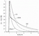
Fig. 1-1 plots the probability of emitting a photon as a function of time for two markers having different lifetimes. The signature represented by probability curve B has a probability of emission that decays more rapidly than the probability of emission of the signature represented by probability curve a. The signature represented by the probability curve B has a shorter time parameter τ or lifetime than the signature represented by the probability curve a. In some embodiments, the marker may have a lifetime in the range of 0.1-20 ns. However, the techniques described herein are not limited to the lifetime of the used markers.
The lifetime of a marker may be used to distinguish among more than one marker, and/or may be used to identify a marker. In some embodiments, a lifetime measurement may be performed in which multiple markers having different lifetimes are excited by an excitation source. As an example, four markers having lifetimes of 0.5, 1, 2, and 3 nanoseconds, respectively, may be excited by a light source that emits light having a selected wavelength (e.g., 635nm, by way of example). The markers may be identified or distinguished from each other based on a measurement of the lifetime of light emitted by the markers.
The lifetime measurement may employ a relative intensity measurement by comparing how the intensity changes over time, as opposed to an absolute intensity value. Thus, the lifetime measurement may avoid some of the difficulties of absolute intensity measurement. Absolute intensity measurements may depend on the concentration of the marker present and may require calibration steps for varying marker concentrations. Conversely, the lifetime measurement may be insensitive to the concentration of the marker.
Embodiments may use any suitable combination of marker features to distinguish a first marker in a set of markers from other markers in the same set. For example, some embodiments may only utilize timing information of the emitted light from the marker to authenticate the marker. In such embodiments, each marker in the selected set of markers has a different emission lifetime than the other markers in the set, and the luminescent markers are all excited by light from a single excitation source. Fig. 1-2A show emission timings from four luminescent markers, wherein the four markers exhibit different average emission lifetimes (τ), according to one embodiment. The probability that a flag is measured to have a particular value of life is referred to herein as the "transmission timing" of the flag. First emission timing 1-101 from the first light emitting marker has a peak probability of having a lifetime at τ 1, second emission timing 1-102 from the second light emitting marker has a peak probability of having a lifetime at τ 2, third emission timing 1-103 from the third light emitting marker has a peak probability of having a lifetime at τ 3, and fourth emission timing 1-104 from the fourth light emitting marker has a peak probability of having a lifetime at τ 4. In this embodiment, the lifetime probability peaks of the four luminescent markers may have any suitable value that satisfies the relationship τ 1< τ 2< τ 3< τ 4. The four timed emission patterns may or may not overlap due to slight variations in the lifetime of a particular lighted sign, as shown in fig. 1-2A. In this embodiment, the excitation wavelengths at which each of the four markers maximally absorbs light from the excitation source are approximately the same, but this need not be the case. With the marker set described above, four different molecules can be labeled with individual markers from the marker set, the markers can be excited with a single excitation source, and the markers can be distinguished from each other by detecting the emission lifetimes of the markers using optical systems and sensors. Although fig. 1-2A show four different markers, it should be understood that any suitable number of markers may be used.
Other embodiments may utilize any suitable combination of marker features to determine the characteristics of the markers in a set of markers. Examples of marking features that may be used include, but are not limited to: excitation wavelength, emission wavelength, and emission lifetime. The combination of the signature features from the phase space and each signature can be represented as a point within this phase space. The markers within a set of markers should be selected such that the "distance" between the markers within the set is sufficiently large so that the detection mechanism can distinguish the markers from the other markers in the set. For example, in some embodiments, a set of markers may be selected, where a subset of markers have the same emission wavelength, but have different emission lifetimes and/or different excitation wavelengths. In other embodiments, a selection of a set of markers may be made, where a subset of markers have the same emission lifetime, but different emission wavelengths and/or different excitation wavelengths. In other embodiments, a selection of a set of markers may be made, where a subset of markers have the same excitation wavelength, but different emission wavelengths and/or different emission lifetimes.
For example, and without limitation, fig. 1-2B illustrate emission spectra from four luminescent markers, two markers having a first peak emission wavelength and two other markers having a second peak emission wavelength, according to one embodiment. The first emission spectrum 1-105 from the first luminescent mark has a peak emission wavelength at λ 1, the second emission spectrum 1-106 from the second luminescent mark also has a peak emission wavelength at λ 1, the third emission spectrum 1-107 from the third luminescent mark has a peak emission wavelength at λ 2, and the fourth emission spectrum 1-108 from the fourth luminescent mark also has a peak emission wavelength at λ 2. In this embodiment, the emission peaks of the four luminescent markers may have any suitable value that satisfies the relationship λ 1< λ 2. In embodiments, for example, where the peak emission wavelengths of more than one luminescent mark are the same, the individual characteristics of each mark having the same emission wavelength must be different. For example, two markers emitting light at λ 1 may have different emission lifetimes. Fig. 1-3A schematically illustrate this in a phase space divided by emission wavelength and emission lifetime. The first mark has an emission wavelength λ 1 and an emission lifetime τ 1, the second mark has an emission wavelength λ 1 and an emission lifetime τ 4, the third mark has an emission wavelength λ 2 and an emission lifetime τ 1, and the fourth mark has an emission wavelength λ 2 and an emission lifetime τ 4. Thus, all four markers in the marker set shown in FIGS. 1-3A are distinguishable from each other. The use of such a marker set allows discrimination between four markers even when the absorption wavelengths of the four markers are the same. Sensors that can detect the time of emission of the photoluminescence as well as the wavelength of the emission can be used.
For example, and without limitation, fig. 1-2C show absorption spectra from four luminescent markers according to another embodiment. In this embodiment, two of the markers have a first peak absorption wavelength and the other two markers have a second peak absorption wavelength. The first absorption spectrum 1-109 of the first luminescent indicia has a peak absorption wavelength at λ 3, the second absorption spectrum 1-110 of the second luminescent indicia has a peak absorption wavelength at λ 4, the third absorption spectrum 1-111 of the third luminescent indicia has a peak absorption wavelength at λ 3, and the fourth absorption spectrum 1-112 of the fourth luminescent indicia has a peak absorption wavelength at λ 4. It should be noted that the markers sharing a common absorption peak wavelength in fig. 1-2C may be distinguished by another other marker characteristic (e.g., emission lifetime). Fig. 1-3B schematically illustrate this in a phase space divided by the absorption wavelength and emission lifetime. The first mark has an absorption wavelength λ 3 and an emission lifetime τ 1, the second mark has an absorption wavelength λ 3 and an emission lifetime τ 4, the third mark has an absorption wavelength λ 4 and an emission lifetime τ 1, and the fourth mark has an absorption wavelength λ 4 and an emission lifetime τ 4. Thus, all four tags in the set of tags shown in FIGS. 1-3A are distinguishable from each other.
The use of such a set of markers allows discrimination between the four markers even when the emission wavelengths of the four markers are indistinguishable. Two excitation sources emitting at different wavelengths or a single excitation source capable of emitting at multiple wavelengths can be used, along with a sensor that can detect the emission time of photoluminescence. If the wavelength of the luminescence for each detected emission event is known, then it can be determined which marker is present. The excitation source may be shifted between a first excitation wavelength and a second excitation wavelength, which is referred to as interleaving. Alternatively, two or more pulses of a first excitation wavelength may be used, followed by two or more pulses of a second excitation wavelength.
The number of excitation sources or excitation wavelengths used to distinguish the markers is not limited to two, and in some embodiments more than two excitation wavelengths or energies may be used to distinguish the markers. In such embodiments, the intensity or number of photons emitted in response to multiple excitation wavelengths may be used to distinguish the markers. A marker may be distinguished among multiple markers by detecting the number of photons emitted in response to exposing the marker to a certain excitation wavelength. In some embodiments, a marker is identified by illuminating the marker with one of a plurality of excitation energies at a time and identifying the excitation energy from the plurality of excitation energies in which the marker emits the highest number of photons. In other embodiments, the number of photons emitted from the marker in response to different excitation energies may be used to identify the marker. A first marker having a probability of emitting a photon in response to a first excitation energy higher than a second excitation energy may be distinguished from a second marker having a probability of emitting a photon in response to a second excitation energy higher than the first excitation energy. Thus, a marker having a distinguishable probability of emitting a certain amount of photons in response to different excitation energies can be identified by simultaneously measuring the emitted photons by exposing the unknown marker to different excitation energies. In such embodiments, the marker may be exposed to a variety of excitation energies and the identification of the marker may be accomplished by determining whether the marker emits any light and/or a particular number of emitted photons. Any suitable number of excitation energy sources may be used. In some embodiments, four different excitation energies may be used to identify among different markers (e.g., four different markers). In some embodiments, three different excitation energies may be used to identify among different markers. Other characteristics of the marker may be used in conjunction with the amount of photons emitted in response to different excitation energies, including emission lifetime and emission spectrum, to distinguish the presence of the marker.
In other embodiments, more than two characteristics of a marker in a marker set may be used to distinguish which marker is present. Fig. 1-4 show illustrative phase spaces divided by absorption wavelength, emission wavelength, and emission lifetime of each marker. In fig. 1-4, eight different markers are distributed in phase space. Four of the eight markers have the same emission wavelength, four different markers have the same absorption wavelength and four different markers have the same emission lifetime. However, when all three features of a logo are considered, each logo may be distinguished from every other logo. Embodiments are not limited to any number of flags. This concept can be extended to include any number of markers that can be distinguished from one another using at least these three marker features.
Although not shown in the figures, other embodiments may determine the characteristics of the luminescent signature based solely on the absorption frequency. Such an implementation is feasible if the excitation light can be tuned to a specific wavelength that matches the absorption spectra of each marker in the marker set. In such an embodiment, the optical system and sensor for guiding and detecting the light emitted from each marker need not be capable of detecting the wavelength of the emitted light. This may be advantageous in some embodiments because it reduces the complexity of the optical system and sensor, as detection of the emission wavelength is not required in such embodiments.
As described above, the present inventors have recognized and appreciated a need to be able to distinguish different illuminated signs from each other using various characteristics of the signs. The type of each feature used to determine the signature features affects the physical means used to perform this analysis. The present application discloses several embodiments of instruments, devices, apparatuses and methods for performing these different experiments.
The present inventors have recognized and appreciated that a low cost disposable integrated device comprising optical components and sensors may be used in conjunction with an instrument comprising an excitation source to measure different characteristics of light emitted in one or more markers used to tag a biological sample to analyze the sample. Using a low cost integrated device may reduce the cost of performing a given biometric. The biological sample is placed on the integrated device and can be discarded when the bioassay is complete. The integrated device interacts with a more expensive multi-use instrument that can be reused with many different single-use integrated devices. Low cost integrated devices that interact with compact portable instruments can be used anywhere in the world without the constraints of high cost biological laboratories that require the expertise of a laboratory to analyze samples. Thus, automated bioanalysis can be brought to areas where quantitative analysis of biological samples could not previously be performed. For example, a blood test of an infant may be performed by: the blood sample is placed on the integrated single use device, the integrated single use device is analyzed in a small portable instrument, and the results are processed for immediate viewing by the user using a computer connected to the instrument. The data may also be transmitted over a data network to a remote location for analysis and/or archived for later clinical analysis. Alternatively, the instrument may include one or more processors for analyzing data acquired from sensors of the integrated device.
Various embodiments are described in more detail below.
I. Overview of the System
The system includes an integrated device and an instrument for interacting with the integrated device. The integrated device includes an array of pixels, wherein a pixel includes a sample well and at least one sensor. The surface of the integrated device has a plurality of sample wells, wherein the sample wells are for receiving samples from a specimen disposed on the surface of the integrated device. A sample may contain multiple samples, and in some embodiments different types of samples. The plurality of sample wells may be designed such that at least a portion of the sample wells are for receiving a sample from the specimen. In some embodiments, these quantities of sample inside the sample wells may be distributed among the sample wells such that some sample wells hold one sample and other sample wells hold zero, more than two samples. For example, the sample may comprise a plurality of single stranded DNA templates, and the sample wells on the surface of the integrated device may receive the single stranded DNA templates. The sample wells of at least a portion of the integrated device can contain single stranded DNA templates. The sample may also contain tagged dntps which then enter the sample well and may allow identification of nucleotides when incorporated into the complementary strand of DNA. In such an example, a "sample" may refer to both single-stranded DNA and tagged dntps that are now incorporated with a polymerase. In some embodiments, the sample may comprise a single stranded DNA template, and the tagged dNTPS may then be introduced into the sample well when nucleotides are incorporated into the complementary strand of DNA inside the sample well. In this way, the timing of nucleotide incorporation can be controlled when introducing tagged dNTPs into the sample well of the integrated device.
Excitation energy is provided from an excitation source located at a location separate from the pixel array of the integrated device. Excitation energy is directed at least partially towards one or more pixels with an element of the integrated device to illuminate an illuminated region inside the sample well. The marker or tag may then emit emission energy when positioned within the irradiation region and in response to being irradiated by the excitation energy. In some embodiments, the one or more excitation sources are part of an instrument of the system, wherein components of the instrument and the integrated device are for directing excitation energy toward the one or more pixels. In other embodiments, one or more excitation sources are located on the integrated device but in separate regions from the array of pixels, and components in the integrated device are for directing excitation energy from the excitation source regions to the one or more pixels.
The emission energy emitted by the sample can then be detected using one or more sensors within a pixel of the integrated device. In some embodiments, the plurality of sensors are sized and arranged to capture a spatial distribution of the emitted energy. In some embodiments, one or more sensors can be used to detect a timing characteristic (e.g., fluorescence lifetime) associated with the emission energy of the sample. The output signals from the one or more sensors may then be used to distinguish one marker from a plurality of markers that may be used to identify the sample within the specimen. In some embodiments, a plurality of excitation energies may be utilized to excite a sample, and an emission energy and/or timing feature emitted by the sample in response to the plurality of excitation energies may distinguish one marker from a plurality of markers.
A schematic overview of the system 2-100 is shown in fig. 2-1A and 2-1B. The system comprises two integrated devices 2-102 interacting with the instruments 2-104. In some embodiments, the instruments 2-104 may include one or more excitation sources 2-106. In some embodiments, the excitation source may be external to both the instrument 2-104 and the integrated device 2-102, and the instrument 2-104 may be configured to receive excitation energy from the excitation source and direct the excitation energy to the integrated device. The integrated device is interconnected with the instrument using any suitable receptacle that accepts the integrated device and holds it in precise optical alignment with the excitation source. The excitation sources 2-106 may be used to provide excitation energy to the integrated devices 2-102. Although the excitation source is illustrated on the instrument in fig. 2-1B, the excitation source may also be located on the integrated device in a region separate from the pixels in some cases. As schematically shown in fig. 2-1B, the integrated device 2-102 has a plurality of pixels, wherein each pixel 2-112 is capable of performing an independent analysis of a sample. Such pixels 2-112 may be referred to as "passive pixels" because the pixels receive excitation energy from an excitation source 2-106 separate from the pixels, where the excitation source excites a plurality of pixels. Each pixel 2-112 has a sample well 2-108 for holding and analyzing a sample, and a sensor 2-110 for detecting emission energy emitted by the sample in response to illumination of the sample by excitation energy provided by the excitation source 2-106. In some embodiments, each sensor 2-110 may include a plurality of sub-sensors, each sub-sensor being for detecting a different wavelength of emission energy from the sample.
The optical elements for directing and coupling the excitation energy to the sample wells 2-108 are located on both the integrated device 2-102 and the instrument 2-104. Such source-to-well elements may include: a grating coupler on the integrated device 2-102 for coupling excitation energy to the integrated device, a waveguide and lens for delivering excitation energy to each pixel 2-112, a plasmonic element on the integrated device, and a dielectric coating for directing excitation energy received from the instrument 2-104 to the sample well 2-108. Furthermore, an optical element located on the integrated device directs the emission energy from the sample well towards the sensor. Such a well-to-sample element may comprise means for directing emission energy into a radiation pattern, wherein the radiation pattern is dependent on the emission energy emitted by the sample in the sample well. Sample well 2-108, a portion of the excitation source-to-well optics, and sample well-to-sensor optics are located on integrated device 2-102. Excitation sources 2-106 and a portion of the excitation source-to-trap components are located in instruments 2-104. In some embodiments, a single component may play a role in coupling excitation energy to the sample wells 2-108 and transferring emission energy from the sample wells 2-108 to the sensors 2-110.
As shown in fig. 2-1B, the integrated device includes a plurality of pixels, each pixel 2-112 being associated with its own individual sample well 2-108 and sensor 2-110. A plurality of pixels may be arranged in an array, and there may be any suitable number of pixels. For example, the integrated device 2-102 may include between 100 and 1,000 pixels according to some embodiments, between 1,000 and 10,000 pixels according to some embodiments, between 10,000 and 100,000 pixels according to some embodiments, between 100,000 and 1,000,000 pixels according to some embodiments, and between 1,000,000 and 10,000,000 pixels according to some embodiments. In some embodiments, fewer or more pixels may be present on the integrated devices 2-102. The integrated devices 2-102 and instruments 2-104 may include multi-channel high-speed communication links for processing data associated with large pixel arrays (e.g., greater than 1000 pixels).
Excitation sources 2-106 may be any suitable excitation source arranged to deliver excitation energy to at least one sample well. In some embodiments, the array of one or more excitation sources is located adjacent to the array of pixels on the same integrated device. In other embodiments, the one or more excitation sources are on a second substrate mounted in close proximity to the substrate on which the array of pixels is formed.
The instruments 2-104 are interconnected to the integrated devices 2-102 via the integrated device interfaces 2-114. The integrated device interfaces 2-114 may include components to position and/or align the integrated devices 2-102 to the instruments 2-104 to improve coupling of excitation energy from the excitation sources 2-106 to the integrated devices 2-102. In some embodiments, the excitation source 2-106 includes multiple excitation sources that are combined to deliver excitation energy to the integrated device 2-102. Multiple excitation sources can be used to generate multiple excitation energies or wavelengths. The integrated device interfaces 2-114 may receive readout signals from sensors located in pixels on the integrated device. Furthermore, the integrated device interfaces 2-114 may be designed such that the integrated device is attached to the instrument by securing the integrated device to the integrated device interfaces 2-114.
The instruments 2-104 include user interfaces 2-116 for controlling the operation of the instruments 2-104. The user interfaces 2-116 are for allowing a user to input information into the instrument, such as commands and/or settings for controlling the operation of the instrument. In some embodiments, the user interface 2-116 may include keys, switches, a dial, and a microphone for voice commands. Further, the user interfaces 2-116 may allow the user to receive feedback regarding the performance of the instrument and/or integrated device (e.g., proper alignment), and/or information obtained based on read-out signals from sensors on the integrated device. In some implementations, the user interfaces 2-116 may utilize speakers to provide feedback for providing audible feedback, and indicator lights and/or display screens for providing visual feedback. In some embodiments, the instruments 2-104 include computer interfaces 2-118 for interfacing with computing devices 2-120. Any suitable computer interface 2-118 and computing device 2-120 may be used. For example, computer interfaces 2-118 may be USB interfaces or firewire interfaces. Computing devices 2-120 may be any general purpose computer, such as a laptop computer or desktop computer. The computer interfaces 2-118 facilitate communication of information between the instruments 2-104 and the computing devices 2-120. Input information for controlling and/or setting the instrument 2-104 may be provided via a computing device 2-120 connected to the computer interface 2-118 of the instrument. Further, output information may be received by computing devices 2-120 via computer interfaces 2-118. Such output information may include feedback regarding the performance of the instruments 2-104 and/or integrated devices 2-112, and information based on the readout signals of the sensors 2-110. The instruments 2-104 may also include processing devices 2-122 for analyzing data received from the sensors 2-110 and/or sending control signals to the excitation sources 2-106. In some embodiments, the processing devices 2-122 may include a general purpose processor, a specialized processor (e.g., a Central Processing Unit (CPU) such as one or more microprocessors or microcontroller cores, a Field Programmable Gate Array (FPGA), an Application Specific Integrated Circuit (ASIC), a custom integrated circuit, a Digital Signal Processor (DSP), or a combination thereof). In some embodiments, the processing of data from the sensors 2-110 may be performed by both the processing device 2-122 and the external computing device 2-120. In other embodiments, computing devices 2-120 may be omitted and the processing of data from sensors 2-110 may be performed only by processing devices 2-122.
A schematic cross-section of an integrated device 3-102 showing a row of pixels is shown in fig. 3-1A. Each pixel 3-112 comprises a sample well 3-108 and a sensor 3-110. The sensors 3-110 may be aligned and positioned with respect to the sample wells 3-112. When the excitation source is coupled to the integrated device, excitation energy is provided to one or more pixels. Fig. 3-1B is a schematic diagram illustrating coupling of excitation sources 3-106 to integrated devices 3-102. In the integrated device 3-102, the excitation source 3-106 provides excitation energy 3-130 (indicated with dashed lines) in the integrated device 3-102. Fig. 3-1B shows the path of excitation energy from the excitation energy source 3-106 to the sample well 3-108 in pixel 3-112. Components located in a separate location from the integrated device can be used to position and align the excitation sources 3-106 to the integrated device. Such components may include optical components, including lenses, mirrors, prisms, apertures, attenuators, and/or optical fibers. Other mechanical components may be included in the instrument to allow control of one or more alignment components. Such mechanical components may include actuators, stepper motors, and/or knobs. The integrated device comprises means for directing the excitation energy 3-130 towards the pixels in the integrated device. Inside each pixel 3-112, excitation energy is coupled to the sample well 3-108 associated with that pixel. Although fig. 3-1B shows the coupling of excitation energy to each sample well in a row of pixels, in some embodiments, excitation energy may not be coupled to all pixels in the row. In some embodiments, the excitation energy may be coupled to a portion of the pixels or sample wells in a row of pixels of the integrated device. The excitation energy may illuminate a sample located inside the sample well. The sample may reach an excited state in response to being irradiated by the excitation energy. The sample may emit emission energy when the sample is in an excited state, and the emission energy may be detected using a sensor. Fig. 3-1B schematically shows the path of the emitted energy 3-140 from the sample well 3-108 to the sensor 3-110 of the pixel 3-112 (shown as a solid line). The sensors 3-110 in pixels 3-112 may be constructed and positioned to detect the emission energy from the sample wells 3-108. In some embodiments, sensors 3-110 may include one or more sub-sensors.
A sample to be analyzed may be introduced into the sample well 3-108 of pixel 3-112. The sample may be a biological sample or any other suitable sample, such as a chemical sample. The sample may comprise a plurality of molecules and the sample trap may be used to separate single molecules. In some cases, the size of the sample well may function to confine a single molecule inside the sample well, allowing measurement of a single molecule. Excitation source 3-106 may be used to deliver excitation energy into sample well 3-108 to excite the sample or at least one luminescent marker attached to or associated with the sample when the sample is inside an excitation region inside sample well 3-108. In a sample of multiple molecules, the type of luminescent marker may be uniquely associated with one molecule type. The luminescent marker may emit emission energy during or after excitation. When multiple markers are used, they may emit light at different characteristic energies. In some embodiments, multiple markers may have different characteristic lifetimes. Further, the plurality of markers may differ in response to a plurality of excitation energies. Markers for a sample can be distinguished by their excitation response, characteristic energy or wavelength, and/or characteristic lifetime. Emissions from the sample may radiate from the sample well 3-108 to the sensor 3-110.
The components may concentrate the emitted energy towards the sensor, in addition or alternatively, spatially separate the emitted energy with characteristic energies or wavelengths. Excitation energy emitted from the excitation source 3-106 may be directed towards the sample well 3-108 in any suitable manner and used to excite at least one sample received in the sample well 3-108. According to some embodiments, excitation sources 3-106 can excite a luminescable sample. The excitation source may provide one or more excitation energies to the sample wells 3-108. In some embodiments, excitation sources 3-106 may excite one or more markers that emit light or emit energy in response to excitation and that are attached to or associated with the sample. The luminescence emitted or energy formed upon excitation may be directed to the sensor 3-110, which sensor 3-110 may be used to detect the intensity and/or timing of the received emission. Non-limiting examples of luminescence are photoluminescence, fluorescence and phosphorescence.
In some embodiments, the integrated device may include components to direct the emission energy into a radiation pattern that depends on the spectral range of the emission energy. The sensor or a sensor area containing a plurality of sub-sensors may detect a spatial distribution of the emitted energy depending on the radiation pattern. Markers emitting different emission energies and/or spectral ranges may form different radiation patterns. The sensor or sensor area may detect information about the spatial distribution of the emitted energy, which may be used to identify one of the plurality of markers.
The one or more transmitted energies may be detected by the sensor and converted into at least one electrical signal. The electrical signals may be communicated along wires in a circuit of an integrated device connected to the instrument through an integrated device interface (e.g., integrated device interfaces 2-114 of instruments 2-104 shown in fig. 2-1B). These electrical signals may then be processed and/or analyzed. The processing or analysis of the electrical signals may be performed on a suitable computing device located on the instrument 2-104 or off the instrument (e.g., on the computing device 2-120 shown in fig. 2-1B).
The integrated device 2-210 may be as shown in fig. 2-2. Electronic, optical, and related structures may all be incorporated onto a single substrate 2-200. The integrated device may include an array of pixels 2-205, and integrated electronic circuitry. The integrated electronic circuit may comprise drive and readout circuitry 2-215 coupled to the sensors of the pixel array, and signal processing circuitry. The signal processing circuitry may include an analog-to-digital converter 2-217, and one or more field programmable gate arrays and/or digital signal processors 2-219. Some embodiments may have more circuit components and some embodiments may have fewer circuit components integrated on the substrate. Although the components of the integrated device are illustrated on a single level in fig. 2-2, the components may be fabricated on multiple levels on the substrates 2-200.
In some embodiments, there may be an optical element (not shown) located on the integrated device, the optical element being arranged to direct and couple excitation energy from one or more excitation sources to the sample well. Such excitation source-to-well elements may include plasmonic structures and other micro-machined structures located adjacent to the sample well. Furthermore, in some embodiments, there may be optical elements located on the integrated device for directing the emission energy from the sample wells to the respective sensors. Such well-to-sample elements may include plasmonic structures and other micromachined structures located adjacent to the sample well. In some embodiments, a single component may function both in coupling excitation energy to the sample well and in delivering emission energy from the sample well to the respective sensor.
In some embodiments, the integrated device may include more than one type of excitation source for exciting the sample at the sample well. For example, there may be multiple excitation sources for generating multiple excitation energies or wavelengths for exciting the sample. In some embodiments, a single excitation source emits multiple wavelengths that can be used to emit excitation of the sample in the sample well. In some embodiments, each sensor at one pixel of the integrated device may include multiple sub-sensors for detecting different emission energy characteristics from the sample.
In operation, parallel analysis of a sample inside a sample well is performed by exciting the sample inside the well with an excitation source and detecting signals emitted from the sample with a sensor. The emission energy from the sample may be detected by the respective sensor and converted into at least one electrical signal. In some embodiments, the one or more formed signals may be processed on an integrated device or communicated to an instrument for processing by a processing device and/or a computing device. Signals from the sample well may be received and processed independently of signals associated with other pixels.
At least one sample inside the well may luminesce when the excitation source delivers excitation energy to the sample well, and the resulting emission may be detected by the sensor. As used herein, the phrase "the sample can luminesce" or "the sample can emit radiation" or "emission from the sample" means that the fluorescent label, marker, or reporter, the sample itself, or a reaction product associated with the sample can produce the emitted radiation.
In some embodiments, the sample can be labeled with one or more markers, and the instrument can be used to distinguish between emissions associated with the markers. For example, the sensor may be used to convert photons from the emitted energy into electrons to form an electrical signal that may be used to distinguish between lifetimes dependent on the emitted energy from a particular marker. By using a tag to label the samples with signatures having different lifetimes, a particular sample can be identified based on the resulting electrical signal detected by the sensor. In some embodiments, components of the integrated device may affect the emission from the sample well to produce a spatial emission profile pattern that is dependent on the emission wavelength. A corresponding sensor for the sample well may be used to detect the spatially distributed pattern from the sample well and generate a signal that is distinguishable between different emission wavelengths, as described in more detail below.
II. Integrated apparatus
The integrated device may be configured to receive excitation energy from an external excitation energy source. In some embodiments, a region of the device can be used to couple to an excitation energy source located remotely from the integrated device. Components of the integrated device can direct excitation energy from the excitation source coupling region to at least one pixel. In some embodiments, at least one waveguide may be used to deliver excitation energy to at least one pixel having a sample well. A sample located inside the sample well may emit emission energy in response to being irradiated with excitation energy. One or more sensors located within the pixel are for receiving the emitted energy.
According to some embodiments, the components and/or layers of the integrated device 3-200 shown in FIG. 3-2 include a sample well 3-203, a waveguide 3-220, and a sensor 3-275 integrated into one device. The sample well 3-203 may be formed in a sample well layer 3-201 of the integrated device 3-200. In some embodiments, the sample well layers 3-201 may be metal. Sample wells 3-203 may have a dimension D that may represent a cross-sectional dimension of the sample well tv . Sample (A)The wells 3-203 may function as nanopores and have one or more sub-wavelength dimensions that result in a field enhancement effect that increases the excitation intensity of the sample in the wells 3-203. The waveguides 3-220 are for delivering excitation energy to the sample wells 3-203 from excitation sources 3-230 located remotely from the integrated 3-200 location. The waveguides 3-220 may be formed in a layer between the sample well layer 3-201 and the sensors 3-275. The design of the integrated device 3-200 allows the sensor 3-275 to collect luminescence emitted from the sample in the sample well 3-203. At least part of the time, the sample absorbs the excitation energy and emits photons having an energy less than the excitation energy, which is referred to as emission energy or luminescence.
Having the sample well 3-203 and the sensor 3-275 on the integrated device 3-200, the optical distance that light travels from the sample well 3-203 to the sensor 3-215 can be reduced. The dimensions of the integrated devices 3-200 or components inside the integrated device may be used for a certain optical distance. The optical properties of the components of the device and/or the material of one or more layers may determine the optical distance between the sample well and the sensor. In some embodiments, the thickness of one or more layers may determine the optical distance between the sample well and the sensor in one pixel. Additionally or alternatively, the refractive index of the material constituting the one or more layers of the integrated device 3-200 may determine the optical distance between the sample well 3-203 and the sensor 3-275 in one pixel. Such optical distance between the sample well and the sensor in one pixel may be less than 1mm, less than 100 microns, less than 25 microns, and/or less than 10 microns. One or more layers may be present between the sample well layer 3-201 and the waveguide layer 3-220 to improve the coupling of excitation energy from the waveguide 3-220 to the sample well 3-203. Although the integrated device 3-200 shown in fig. 3-2 shows only a single layer 3-210, multiple layers may be formed between the sample well 3-203 and the waveguide 3-220. Layers 3-210 may be formed with optical properties to improve the coupling of excitation energy from the waveguide 3-220 to the sample well 3-203. Layers 3-210 may be used to reduce scattering and/or absorption of excitation energy and/or increase luminescence from the sample in sample wells 3-203. According to some embodiments, the layers 3-210 may be optically transparent so that light may travel to and from the sample wells 3-203 with little attenuation. In some embodiments, layers 3-210 may be formed using dielectric materials. In some embodiments, excitation energy coupling means may be provided within the layers 3-210 and/or at the interface between the layers 3-210 and the sample well layer 3-201 to improve the coupling of excitation energy from the waveguide 3-220 to the sample well 3-203. As an example, energy harvesting components 3-215 formed at the interface between the sample well layer 3-201 and the layer 3-210 may be used to improve the coupling of excitation energy from the waveguide 3-220 to the sample well 3-203. The energy harvesting components 3-215 are optional, and in some embodiments, the configuration of the waveguides 3-220 and sample wells 3-203 may allow for sufficient coupled excitation energy in the absence of the excitation energy harvesting components 3-215.
Luminescence or energy emitted from the sample in the sample well 3-203 may be transferred to the sensor 3-275 in a variety of ways, some examples of which are described in more detail below. Some embodiments may utilize optical components to increase the likelihood that light of a particular wavelength is directed to an area or portion of the sensor 3-275 dedicated to detecting light of that particular wavelength. The sensors 3-275 may include portions for simultaneously detecting different wavelengths of light that may correspond to emissions from different illuminated signs.
There may be one or more layers between the sample well 3-203 and the sensor 3-275 that may be used to improve the collection of luminescence from the sample well 3-203 to the sensor 3-275. The light emitting directing component may be located at the interface between the sample well layer 3-201 and the layer 3-210. The energy harvesting component 3-215 may concentrate the emission energy towards the sensor 3-275, in addition or alternatively may spatially separate emission energies having different characteristic energies or wavelengths. Such an energy-harvesting component 3-215 may comprise a grating structure for directing luminescence towards the sensor 3-275. In some embodiments, the grating structure may be a series of concentric rings or a "bullseye" grating structure configuration. The concentric circular grating may protrude from the bottom surface of the sample well layer 3-201. These circular gratings may function as plasmonic elements that may be used to reduce the diffusion of signal light and direct signal light towards the associated sensor 3-275. Such a bullseye grating may more efficiently direct the luminescence towards the sensors 3-275.
Layers 3-225 may be formed adjacent to the waveguide. The optical properties of layers 3-225 may be selected to improve the collection of luminescence from the sample well to sensors 3-275. In some embodiments, layers 3-225 may be dielectric materials. A barrier may be formed between the sample well layer 3-201 and the sensor 3-275. The baffle 3-240 may be configured such that the sensor 3-275 receives luminescence corresponding to the sample well 3-203 and reduces luminescence, and reflected/scattered excitation, from other sample wells. The filter element 3-260 may be positioned and configured to reduce excitation energy from reaching the sensor 3-275. In some embodiments, filter elements 3-260 may include a filter that selectively passes the emission energy of one or more markers used to tag the sample. In embodiments using an array of sample wells and an array of sensors, wherein each sample well has a corresponding sensor, a baffle corresponding to each sample well can be formed to reduce luminescence from other sample wells and to reflect and/or scatter excitation light collected by the sensors corresponding to the sample wells.
One or more layers may be formed between the waveguide 3-220 and the sensor 3-275 to reduce the transmission of excitation energy to the sensor. In some embodiments, a filter element may be formed between the waveguide 3-220 and the sensor 3-275. Such a filter element may be used to reduce the transmission of excitation energy to the sensors 3-275 while allowing luminescence from the sample well to be collected by the sensors 3-275.
The one or more transmitted energies may be detected by the sensors 3-275 and converted into at least one electrical signal. One or more electrical signals may be transferred along one or more rows or columns of conductive lines (not shown) to integrated electronic circuits on substrates 3-200 for subsequent signal processing.
The above description of fig. 3-2 is a diagrammatic illustration of components of a portion of an apparatus according to some embodiments. In some embodiments, one or more elements of fig. 3-2 may be absent or in a different location. The components of the integrated device 3-200 and the excitation source 3-230 are described in more detail below.
A. Excitation source coupling region
The integrated device may have an excitation source coupling region for coupling with an external excitation energy source and directing excitation towards at least one pixel in a pixel region of the integrated device. The excitation source coupling region may include one or more structures for coupling light into the at least one waveguide. Any suitable mechanism for coupling excitation energy into the waveguide may be employed.
In some embodiments, excitation energy from an external excitation source can be coupled to a waveguide of the integrated device through edge coupling. The edge of the integrated device may comprise an end of the waveguide such that an external excitation source located near the end of the waveguide may couple light into the waveguide. In such embodiments, fabrication of the excitation source coupling region may include positioning an end of the waveguide at an edge of the integrated device. Fig. 4-1A shows an example of edge coupling. The optical fiber 4-106 for propagating the excitation energy is located near the edge of the integrated device 4-102 where the end of the waveguide 4-104 of the integrated device 4-102 is located so that the optical fiber 4-106 can couple light into the waveguide 4-104. In such embodiments, monitoring the alignment of the optical fibers 4-106 or other excitation sources with the waveguides 4-104 can increase the amount of light provided by the optical fibers to the waveguides.
In some embodiments, a prism may couple light to a waveguide. The light may be guided and refracted by the prism to match the optical phase frequency of the propagating waveguide mode. The refractive index of the material used for the prism may be selected to improve coupling with the waveguide. In some cases, the prism has a higher index of refraction and a narrower slot relative to the waveguide. In other embodiments, the light may be directly coupled to one end of the waveguide. The edges of the integrated device may be sufficiently polished to allow focusing and alignment of the light into the waveguide.
The excitation source coupling region of the integrated device can include structural components for coupling with an external excitation source. The integrated device may include a grating coupler for coupling with an external excitation source, the grating coupler being located proximate to a surface of the integrated device and directing light toward at least one waveguide of the integrated device. Features of the grating coupler, such as size, shape, and/or grating configuration, may be formed to improve coupling of excitation energy from the excitation source to the waveguide. The grating coupler may include one or more structural members, wherein the spacing between the structural members may function to propagate light. One or more size grating couplers may provide a desired coupling of light having a certain characteristic wavelength.
The integrated device may also include a waveguide having a tapered region at one end of the waveguide. One or more dimensions of the waveguide perpendicular to the direction of propagation of light in the waveguide may be larger at one end of the waveguide, thereby forming a tapered region of the waveguide. In some embodiments, the tapered region of the waveguide may have a dimension perpendicular to light propagation and parallel to the surface of the integrated device that is larger at one end of the waveguide and becomes smaller along the length of the waveguide. In embodiments including a grating coupler, the tapered region may be located proximate to the grating coupler such that the larger end of the tapered region is located closest to the grating coupler. The tapered region may be sized and shaped to improve coupling of light between the grating coupler and the waveguide by expanding one or more dimensions of the waveguide to allow improved mode overlap with the waveguide of the grating coupler. In this way, an excitation source located in close proximity to the surface of the integrated device can couple light into the waveguide using a grating coupler. This combination of grating couplers and waveguide taper structures may allow for more tolerance in alignment and positioning of the excitation source and the integrated device.
An exemplary integrated device having a grating coupler and a waveguide with a tapered region is shown in fig. 4-1B. The integrated device 4-100 has an excitation source coupling region that includes a waveguide with a tapered region 4-114 and a grating coupler 4-116. The tapered region 4-114 has one end of larger dimension parallel to the surface 4-112 of the integrated device 4-100 and perpendicular to the light propagation along the waveguide. The end of the tapered region 4-114 may be sized and shaped to provide suitable coupling between the grating coupler 4-116 and the waveguide. An optical fiber 4-120 or other suitable excitation source positioned relative to the grating coupler 4-116 may couple excitation energy to the waveguide.
The grating coupler may be located in a region of the integrated device that is external to the pixels of the integrated device. On the surface of the integrated device, the sample well of each pixel can occupy a surface area separate from the excitation source coupling region. An excitation source located near a surface of the excitation source coupling region may be coupled to the grating coupler. The sample well may be located separately from the excitation source coupling region to reduce interference of light from the excitation source with the pixel performance. The grating coupler of the integrated device may be formed inside one or more layers of the integrated device including the waveguide. As such, the excitation source coupling region of the integrated device may include a grating coupler in the same plane of the integrated device as the waveguide. The grating coupler may be configured for a particular set of beam parameters, including beam width, angle of incidence, and/or polarization of the incident excitation energy.
A cross-sectional view of the integrated device 4-200 is shown in fig. 4-2. The integrated device 4-200 comprises at least one sample well 4-222 formed in a layer 4-223 of the integrated device 4-200. The integrated device 4-200 comprises a grating coupler 4-216 and a waveguide 4-220 formed in substantially the same plane as the integrated device 4-200. In some embodiments, the grating coupler 4-216 and the waveguide 4-220 are formed from the same layer of the integrated device 4-200 and may comprise the same material. The excitation source coupling region 4-201 of the integrated device 4-200 includes a grating coupler 4-216. As shown in fig. 4-2, sample well 4-222 is located on the surface of integrated device 4-200 outside excitation source coupling region 4-201. An excitation source 4-214 positioned relative to integrated device 4-200 can provide excitation energy incident on a surface 4-215 of integrated device 4-200 within excitation source coupling region 4-201. By positioning the grating coupler 4-216 inside the excitation source coupling region 4-201, the grating coupler 4-216 can couple excitation energy from the excitation source 4-214 and couple the excitation energy to the waveguide 4-220. The waveguides 4-220 are for propagating excitation energy into the vicinity of one or more sample wells 4-222.
The grating coupler may be constructed of one or more materials. In some embodiments, the grating coupler may include alternating regions of different materials along a direction parallel to the direction of light propagation in the waveguide. As shown in fig. 4-2, the grating coupler 4-216 comprises a structure surrounded by material 4-224. The one or more materials comprising the grating coupler may have one or more refractive indices suitable for coupling and propagating light. In some embodiments, a grating coupler may include a structure composed of one material having a larger index of refraction surrounded by a material. As an example, a grating coupler may include a structure composed of silicon nitride and surrounded by silicon dioxide.
Any suitable size and/or grating pitch may be used to form the grating coupler. The grating coupler 4-216 may have a dimension perpendicular to the propagation of light through the waveguide (e.g., in the y-direction) of about 50nm, about 100nm, about 150nm, or about 200nm, as shown in fig. 4-2. The spacing between the structures of the grating coupler, along a direction parallel to the direction of light propagation in the waveguide (e.g., along the z-direction), as shown in fig. 4-2, may have any suitable distance. The pitch of the grid lines may be about 300nm, about 350nm, about 400nm, about 420nm, about 450nm, or about 500 nm. In some embodiments, the grating pitch is variable within the grating coupler. The grating coupler 4-216 may have one or more dimensions substantially parallel to the surface 4-215 of the integrated device 4-200 that provide a suitable area for coupling with an external excitation source 4-214. This area of grating coupler 4-216 may coincide with one or more dimensions of the beam from excitation source 4-214 such that the beam overlaps with grating coupler 4-215. The grating coupler may have a region for a beam diameter of about 10 microns, about 20 microns, about 30 microns, or about 40 microns.
Cross-sectional views of a portion of an exemplary excitation source coupling region of an integrated device are shown in fig. 4-3A. The excitation source coupling region comprises a grating coupler 4-326 and a reflective layer 4-336 for reflecting excitation light back through the grating coupler 4-326 towards the grating coupler 4-326. The grating coupler 4-326 may comprise a structure having a grating pitch, represented by Λ, along the z-direction shown in fig. 4-3A. These structures may have a linear, curved, or any other suitable shape. In some embodiments, the grating coupler 4-326 may have a dimension along the y-direction similar to that of the waveguide 4-330, as represented by the arrows on either side of the waveguide 4-330. The grating coupler 4-326 is surrounded by the region 4-324, and the combination of the materials comprising the grating coupler 4-324 and the region 4-324 may provide the desired coupling of light into the waveguide 4-330. The refractive index of the waveguide 4-330, the grating coupler 4-326, and/or the surrounding material 4-324 may affect the coupling of excitation energy to the waveguide and the overall coupling efficiency of excitation energy to the waveguide 4-330. The excitation source coupling region of the integrated device may have a coupling efficiency greater than about 50%. The grating coupler 4-326 may be used to excite one or more characteristics of the incident beam of energy 4-314, including characteristic wavelength, beam diameter (represented by the arrow), and beam angle of incidence (represented by θ). The grating coupler 4-326 may be configured for a beam having a beam diameter of about 10 microns, about 20 microns, about 30 microns, or about 40 microns. The grating couplers 4-326 may be configured for light beams having an incident angle of about 2 degrees, about 5 degrees, or about 7 degrees. The grating couplers 4-326 may be used to couple excitation energy of a certain polarization, such as TM or TE polarized light.
A simulation of optical coupling from a light beam into a waveguide using a grating coupler is shown in fig. 4-3B. The waveguide and grating coupler are located at approximately 0 along the z-axis on the y-axis. The beam is at an angle of incidence of about 5 degrees with respect to the y-direction and has a diameter of 20 microns. The waveguide used in this simulation had a height (in the y-direction) of 100nm and the fixed-stage coupler had a grating pitch of 420 nm. The waveguide and grating coupler structures have a refractive index of about 1.87. The material surrounding the waveguide and the grating structure has a refractive index of about 1.45. Fig. 4-3B show the light intensity of the light beam coupled into the grating coupler and the waveguide, and the mode of the light in the waveguide is shown by the darker regions.
The tapered region of the waveguide and the relative positioning of the tapered region and the grating coupler of one or more dimensions may provide sufficient coupling of excitation energy into the waveguide. The curvature and chirp of the tapered region may accommodate convergence and/or divergence of the propagation of incident excitation energy to the waveguide. A plan view of an exemplary waveguide layer including grating couplers 4-316 and tapered waveguide regions 4-318 is shown in fig. 4-3C. The tapered waveguide regions 4-318 have dimensions perpendicular to the propagation of light and gradually decrease from right to left in the plane of fig. 4-3C to achieve the dimensions of the waveguides 4-320. The grating coupler 4-316 may have a region in the plane of fig. 4-3C suitable for coupling with an external excitation source. The alignment of the beam of excitation energy with the grating coupler 4-316 is such that the beam substantially overlaps the region of the grating coupler 4-316 to improve the coupling of the excitation energy into the waveguide 4-320. The arrangement of the tapered regions 4-318 relative to the grating couplers 4-316 may provide suitable coupling efficiency. The angles of the tapered regions 4-318 and the grating couplers 4-316 may be selected to improve the coupling efficiency of excitation energy from the excitation source to the waveguides 4-320 by reducing the loss of excitation energy (due to the reduced size of the waveguides perpendicular to the propagation of light).
The integrated device may include a layer formed on a side of the grating coupler opposite the excitation source for reflecting light. The layer may reflect excitation energy passing through the grating coupler towards the grating coupler. By including this layer in the integrated device, the coupling efficiency of the excitation energy into the waveguide can be improved. One example of a reflective layer is layers 4-218 of integrated device 4-200 shown in fig. 4-2, and layers 4-336 shown in fig. 4-3A. Layers 4-218 are located inside the excitation source coupling region 4-201 of the integrated device 4-200 and are used to reflect light towards the grating coupler 4-216. Layers 4-218 are formed near one side of the grating coupler 4-216 opposite the incident excitation energy from the excitation source 4-214. Positioning the layers 4-218 outside the pixels of the integrated device 4-200 may reduce the interference of the layers 4-218 with the performance of each pixel. Layers 4-218 may comprise any suitable material. Layers 4-218 are substantially reflective to one or more excitation energies. In some embodiments, this layer may comprise Al, AlCu, and/or TiN.
B. Waveguide
The integrated device may include one or more waveguides that are one or more sample wells for delivering a desired amount of excitation energy to the integrated device. The waveguide is positioned proximate to the one or more sample wells such that a portion of the excitation energy is coupled to the one or more sample wells as the excitation energy propagates along the waveguide. The waveguide may couple excitation energy to a plurality of pixels and act as a bus waveguide. For example, a single waveguide may deliver excitation energy to a row or column of pixels of an integrated device. In some embodiments, a waveguide may be utilized to propagate excitation energy having a plurality of characteristic wavelengths. One pixel of the integrated device may include other structures (e.g., microcavities) for directing excitation energy from the waveguide toward the vicinity of the sample well. In some embodiments, the waveguide can carry an optical mode having an evanescent tail for extending into and/or in a region near the sample well. Other energy coupling structures located near the sample well may couple energy into the sample well from an evanescent tail.
One or more dimensions of the waveguide of the integrated device may provide a desired propagation of excitation energy along the waveguide and/or into one or more sample wells. The waveguide may have a dimension perpendicular to the propagation of light and parallel to the plane of the waveguide, which may be considered as a cross-sectional width. The waveguide may have a cross-sectional width of about 0.4 microns, about 0.5 microns, about 0.6 microns, about 0.65 microns, about 0.8 microns, about 1 micron, or about 1.2 microns. The waveguide may have a dimension perpendicular to the light propagation and perpendicular to the plane of the waveguide, which may be considered as a cross-sectional height. The waveguide may have a cross-sectional height of about 0.05 microns, about 0.1 microns, about 0.15 microns, about 0.16 microns, about 0.17 microns, about 0.2 microns, or about 0.3 microns. In some embodiments, the waveguide has a cross-sectional width that is greater than the cross-sectional height. The waveguide may be located at some distance from one or more sample wells in the integrated device, such as distance D between sample well 4-222 and waveguide 4-220 as shown in fig. 4-2, which is about 0.3 microns, 0.5 microns, or about 0.7 microns.
In one exemplary embodiment, the waveguide may have a cross-sectional width of about 0.5 μm and a cross-sectional height of about 0.1 μm, and be located about 0.5 μm below the sample well layer. In another exemplary embodiment, the waveguide may have a sectional width of about 1 μm and a sectional height of 0.18 μm, and be located at 0.3 μm below the sample well layer.
The waveguide may be sized to support a single transverse radiation mode or may be sized to support multiple transverse radiation modes. In some embodiments, one or more dimensions of the waveguide may function such that the waveguide maintains only a single transverse mode and may selectively propagate a TE or TM polarization mode. In some embodiments, the waveguide may have a highly reflective portion formed on an end thereof so that it supports a longitudinal standing wave mode inside the waveguide. By supporting one mode, the waveguide can have reduced mode interference effects from cross-coupling of modes with different propagation constants. In some embodiments, the highly reflective portion comprises a single highly reflective surface. In other embodiments, the high reflection portion includes a plurality of reflective structures that collectively result in high reflectivity. The waveguide can be used to divide excitation energy from a single excitation source with a higher output intensity using a waveguide beam splitter to form multiple excitation energy beams from the single excitation source. Such an optical beam splitter may include an evanescent coupling mechanism. Additionally or alternatively, photonic crystals may be used in waveguide structures to improve propagation of excitation energy and/or in materials surrounding the waveguide to reduce scattering of excitation energy.
The position and arrangement of the waveguide relative to other components in one pixel of the integrated device may be used to improve the coupling of excitation energy towards the sample well, improve the harvesting of emission energy by the sensor, and/or reduce signal noise introduced by the excitation energy. The waveguide may be sized and/or positioned relative to the sample well to reduce interference of excitation energy propagating in the waveguide with emission energy emanating from the sample well. The positioning and arrangement of the waveguides in the integrated device may depend on the refractive index of the waveguides and the material surrounding the waveguides. For example, the size of the waveguide perpendicular to the direction of light propagation along the waveguide and within the plane of the waveguide may be reduced so that a significant amount of the emitted energy from the sample well passes through the waveguide as the emitted energy propagates to the sensor of the pixel. In some embodiments, the distance between the sample well and the waveguide and/or the waveguide thickness may be selected to reduce reflections from one or more interfaces between the waveguide and the surrounding material. According to some embodiments, the reflection of the emitted energy by the waveguide may be reduced to less than about 5% in some embodiments, less than about 2% in some embodiments, and less than about 1% in some embodiments.
The ability of the waveguide to propagate excitation energy may depend on the material used for the waveguide and the material surrounding the waveguide. Thus, the waveguide structure may be enclosedIncluding core material (e.g., waveguides 4-220), and cladding material (e.g., regions 4-224 shown in fig. 4-2). Both the waveguide and the material surrounding the material may allow propagation of excitation energy having a characteristic wavelength through the waveguide. The material of the waveguide or surrounding material may be selected for a particular refractive index or combination of refractive indices. The waveguide material may have a lower index of refraction than the surrounding waveguide material. Exemplary waveguide materials include: silicon nitride (Si) x N y ) Silicon oxynitride, silicon carbide, tantalum oxide (TaO) 2 ) And aluminum dioxide. Exemplary surrounding waveguide materials include silicon dioxide (SiO) 2 ) And silicon oxide. The waveguide and/or the surrounding material may comprise one or more materials. In some cases, a desired refractive index for the waveguide and/or surrounding material may be obtained by forming the waveguide and/or surrounding material to comprise more than one material. In some embodiments, the waveguide comprises silicon nitride and the surrounding material comprises silicon dioxide.
In one exemplary embodiment, the waveguide comprises silicon nitride and has a refractive index of about 1.90 and a cross-sectional height of about 100nm, and the surrounding material comprises silicon dioxide and has a refractive index of about 1.46. In some embodiments, a waveguide that may have a refractive index of about 1.88 may be used while the surrounding material has a refractive index of about 1.46. In such embodiments, the lower refractive index for the waveguide may reduce optical losses. In another exemplary embodiment, the waveguide comprises a silicon nitride core and a silicon dioxide cladding and is for propagating excitation energy having a characteristic wavelength of 635 nm. The core may have a refractive index of 1.99 and dimensions of 100nm x 500 nm.
The waveguides of the integrated device may be formed to have a desired degree of uniformity within one waveguide and/or among multiple waveguides. Uniformity within the integrated device may be achieved by fabricating the core and/or cladding with waveguide structures of substantially similar size and/or refractive index along one waveguide and among multiple waveguides. Furthermore, waveguides can be formed in a repeatable manner in different integrated devices by ensuring repeatable manufacturing processes in order to achieve a certain degree of compliance in the different devices. The variation in cross-sectional height of the waveguide and/or waveguides may be less than about 2%, less than about 3%, or less than about 4%. The variation in the refractive index of the waveguide and/or waveguides may be less than about 0.5%, less than about 1%, or less than about 2%. The variation in the refractive index of the surrounding material or cladding of the waveguide and/or waveguides may be less than about 0.5%, less than about 1%, or less than about 2%.
The waveguide may be located in one pixel between the sample well and one or more sensors. For example, as shown in FIG. 4-2, a waveguide 4-220 is positioned between the sample well 4-222 and a layer 4-230 comprising at least one sensor. In some embodiments, the sample wells 4-222 may be located between the waveguide and the sensor. The waveguide may be aligned with the sensor, for example, in a center-to-center manner, such that the center of the waveguide is approximately aligned with the center of the sample well. In some embodiments, the waveguide may be displaced by a distance from a position that is center-to-center aligned with the sample well. In some embodiments, two substantially parallel waveguides may deliver excitation energy of the same or different wavelengths to one pixel, and a sample well may be located between the two waveguides. In some embodiments, multiple waveguides at different heights inside the integrated device can direct excitation energy towards the vicinity of one or more sample wells located on the integrated device.
One or more waveguides of the integrated device may include a bend. The curved portion of each waveguide may provide a desired arrangement of waveguides and/or pixels so that a sufficient amount of excitation energy is coupled to one or more sample wells of the integrated device. The design of the waveguide bends can balance the excitation energy losses by using the bending and spatial dimensions of each bend. Furthermore, with proper design, bends inside the waveguide can also be used to filter out part of the propagating light. A portion of the waveguide is designed to: with filtering provided by a certain radius of curvature provided by the curvature in the waveguide to reduce light of one polarization. This bending can be used to select for particular polarization modes, such as TM and TE. In some embodiments, the bend can be used to filter out and/or attenuate TM modes and preserve TE modes. Fig. 4-4 plot optical loss due to bending as a function of radius of curvature for waveguide bends having a cross-sectional height of 100nm and widths of 300nm, 400nm, 500nm, 700nm, and 1000 nm. As an example, to achieve a loss of at least 0.1dB/90 degree bend, a waveguide having a 500nm cross-sectional width may have a bend radius of greater than about 35 microns, or a waveguide having a 700nm cross-sectional width may have a bend radius of greater than about 22 microns.
Dividing each waveguide from a single waveguide into multiple waveguides may allow excitation energy to reach multiple rows or columns of sample wells in an integrated device. An excitation source may be coupled to the input waveguide, and the input waveguide may be divided into a plurality of output waveguides, wherein each output waveguide delivers excitation energy to a row or column of sample wells. Any suitable technique for dividing and/or combining the waveguides may be employed. Such waveguide splitting and/or combining techniques may include star splitters or couplers, Y-splitters, and/or evanescent wave couplers. Additionally or alternatively, a multi-mode interference type beam splitter (MMI) may be used to divide and/or combine the waveguides. One or more of these waveguide partitioning and/or combining techniques may be used to direct excitation energy to the sample well.
An exemplary star coupler 4-500 is shown in fig. 4-5. Two different wavelengths of light can be input to the star coupler using a single waveguide or two waveguides 4-501 and 4-502 as shown in fig. 4-5. The size and shape of the input waveguides can be used to adjust the spread of each excitation beam individually to match at the output waveguides 4-504 to increase the likelihood of achieving similar power distributions in the output waveguides 4-504. The star coupler comprises a free propagation region 4-503, which may be embodied as a slab waveguide. The free propagation regions 4-503 are high multi-mode regions that allow the input light to propagate substantially freely in the plane of the slab waveguide. The free propagation regions 4-503 may have a width of, for example, 300-400 microns from the first output waveguide to the last output waveguide.
The coupling of excitation energy to the output waveguides 4-504 can be adjusted using various parameters of the star coupler, including one or more dimensions of the individual components of the star coupler. For example, the size of the transverse cross-section of each input waveguide 4-501 and 4-502, the size of the transverse cross-section of each output waveguide 4-504, and the distance of each output waveguide 4-504 from the input waveguides can be parameters of the star coupler to adjust to improve the coupling of excitation energy to the output waveguides 4-504. In some embodiments, the star coupler may be formed such that the output waveguides 4-504 have substantially the same power distribution relative to each other. In some implementations, the output waveguides near the outer edges of the star coupler can have different dimensions than the output waveguides near the center. For example, waveguides near the edge may have a larger lateral cross-sectional area, thereby collecting more light than output waveguides near the center of the star coupler (which have a smaller lateral cross-sectional area). In some embodiments, the distance of the output waveguide from the input waveguide may vary. For example, as shown in FIGS. 4-5, the output waveguides near the edges may have a distance from the input waveguides 4-501 and 4-502 that is less than the output waveguides near the center of the star coupler.
The star coupler 4-500 may have any suitable number of output waveguides. In some embodiments, a single star coupler distributes excitation energy throughout the integrated device. The number of output waveguides is therefore equal to the number of rows of pixels in the integrated device. For example, there may be 128 output waveguides. In other embodiments, more than one star coupler may be used. In such an embodiment, the first star coupler may have 64 output waveguides and the second star coupler may have 64 output waveguides, such that the combination of the first and second star couplers provides excitation energy to 128 rows of pixels in the integrated device.
In some embodiments, rather than having an input waveguide, one or more grating couplers may directly couple excitation energy into a free propagation region of a star coupler having multiple output waveguides. A single grating coupler may be utilized to couple multiple wavelengths to the free propagation region of the star coupler. To this end, light of different wavelengths may be incident on the grating coupler at different angles. In some embodiments, multiple grating couplers may be utilized to couple excitation energy of different wavelengths. For example, one grating coupler may be used for each excitation wavelength. Instead of coupling light into an input waveguide that propagates light to the star coupler, the grating coupler constructed as part of the free propagation region may operate in a manner similar to one of the grating couplers described above, with the light being coupled directly into a slab waveguide, e.g., 4-603, that forms the free propagation region.
Another exemplary configuration of a star coupler is shown in fig. 4-6. Light of two wavelengths may be input to the star coupler using grating couplers 4-605 and 4-606 connected to waveguides 4-609 and 4-610, respectively. The grating couplers 4-605 and 4-606 and the waveguides 4-609 and 4-610 may be utilized to reduce the loss of excitation energy by reducing the number of bends and/or selecting bend angles for improving the propagation of excitation energy towards the free propagation region 4-607. The output waveguides 4-608 from the star coupler may be configured in any suitable manner to provide excitation energy to a row of pixels. In the example shown in fig. 4-6, there are 32 output waveguides. The lateral cross-sectional area of the output waveguide 4-608 near the free propagation region 4-607 may vary such that the output waveguide near one end of the free propagation region 4-607 has a lateral cross-sectional area greater than the output waveguide near the center of the free propagation region 4-607. For example, as shown in FIGS. 4-6, the output waveguide 4-608 a has a larger lateral cross-sectional area than the output waveguide 4-608b located closer to the center of the free propagation region 4-607. This change in lateral cross-sectional area in each output waveguide 4-608 may improve the distribution of excitation energy in each output waveguide 4-608 and, in some embodiments, allow a substantially similar amount of excitation energy to be delivered by each output waveguide to a row of pixels. In this way, multiple rows of pixels may receive a substantially similar amount of excitation energy in each row of pixels.
The design for waveguide division may be selected based on the efficiency of the division technique for that number of output waveguides. If the splitting efficiency is higher, more output waveguides can be produced and only a single splitting step can be performed. In some embodiments, a single output waveguide from the splitter may correspond to each row of sample wells. Some embodiments include multiple partitioning steps to obtain a sufficient number of waveguides for delivering excitation energy to a portion of a sample well of an integrated device. In some embodiments, the waveguide may be further divided into a plurality of waveguides using a multi-mode interference splitter (MMI). In an MMI, an input waveguide may be divided into a plurality of output waveguides, where an MMI of one or more dimensions may determine the number of output waveguides and/or the amount of excitation energy delivered to the output waveguides. For example, as shown in FIGS. 4-7, MMI splitter 4-707 is used to provide outputs 4-708 from inputs 4-710. Outputs 4-708 may be coupled to waveguides for propagating excitation energy to rows of sample wells. In some embodiments, the MMI splitter 4-707 can have 280 outputs coupled to waveguides for propagating excitation energy to the 280 rows of sample wells. In some embodiments, the MMI splitter is to receive excitation energy from multiple inputs and to direct the excitation energy to multiple outputs. As shown in fig. 4-7, the MMI splitter 4-717 is coupled to a plurality of inputs 4-720 and provides a plurality of outputs 4-718. In such an embodiment, the number of outputs 4-718 may be greater than the number of inputs 4-720. In some embodiments, the inputs 4-720 may provide different excitation energies to the MMI splitters 4-717. In other embodiments, the division of each waveguide may be performed in multiple division steps. As an example, two sets of multimode interference splitters may be used for splitting, wherein the output waveguides from the first MMI splitter are used as inputs to the second MMI splitter. For example, as shown in fig. 4-7, an MMI splitter 4-727 divides the input waveguide 4-730 into a plurality of outputs, including an output 4-728 coupled to the MMI splitter 4-737 for providing an output 4-738. In some embodiments, an MMI splitter 4-727 may provide 35 outputs and divide each output into 8 output waveguides using another MMI splitter (e.g., 4-737). Because each of the middle 35 waveguides is divided into 8 waveguides, 280 waveguides are formed in this non-limiting example.
In some embodiments, a plurality of input waveguides may be cross-coupled in an MMI splitter, forming output waveguides for coupling light to a sample well of an integrated device. On such an integrated device, there may be multiple grating couplers coupled with multiple excitation sources. The cross-coupled MMI is used to couple multiple excitation sources together and form multiple output waveguides, as shown in fig. 4-7. Each input waveguide of the plurality of input waveguides may begin with one of the grating couplers to couple light from one excitation source to the MMI splitter. Such cross-coupling of multiple excitation sources may improve the robustness of the system to prevent excitation sources from degrading and/or failing. For example, if one of the multiple excitation sources ceases to produce excitation energy, the other excitation source may be utilized to provide sufficient excitation energy in order to obtain a desired level of performance of the integrated device. A compensation mechanism may also be included that compensates for the reduction in excitation energy due to one or more excitation sources by increasing the intensity provided by the remaining active excitation sources.
Techniques for dividing and/or combining waveguides may be selected to reduce losses, including insertion losses, of excitation energy when the waveguides are divided and/or composed. The insertion loss that occurs as a result of dividing and/or combining the waveguides may be about less than 10%, about less than 20%, or about less than 30%. Techniques for dividing the waveguides may allow for approximately uniform division of excitation energy among the plurality of output waveguides, thereby distributing excitation energy evenly among the output waveguides. Techniques for combining waveguides may allow for a substantially uniform relative distribution of excitation energy from multiple input waveguides in each output waveguide. In some embodiments, the uniformity in the output waveguide may be about less than 10%, about less than 20%, or about less than 30%. The technique used to design the waveguide may be selected for a certain tolerance in manufacturing parameters, including waveguide cross-sectional height, cross-sectional width, and/or refractive index of the waveguide.
One or more dimensions of the MMI splitter affect the number of output waveguides and/or the efficiency of waveguide division and/or combining. Designing the MMI splitter may include sizing the MMI splitter to have a certain number of output waveguides and/or a certain splitting efficiency. Fig. 4-8 show simulations of intensity waveforms for light inside an exemplary MMI splitter for receiving light from input waveguides and directing the light into eight output waveguides. In this example, the input and output waveguides have a cross-sectional width of 500nm, and the dimensions of the MMI splitter have a width W of 16.35 microns and a length L of 84.28 microns. By measuring the light delivered at each output waveguide, coupling uniformity and/or efficiency can be measured. For the exemplary MMI splitter shown in fig. 4-8, the strength of the eight output waveguides can vary by up to about 0.1%.
In some embodiments, the grating coupler may be configured to direct input light into a plurality of output waveguides. Fig. 4-9A illustrate a foil grating coupler that may be used to couple light having one or more wavelengths into a plurality of output waveguides 4-904. The thin-sheet grating is a linear grating structure that is much wider than the wavelength of light (e.g., hundreds of microns wide). Which is formed of alternating layers of dielectric material such as silicon nitride and silicon oxide. In some embodiments, multiple wavelengths may be coupled to the sheet grating by emitting different wavelengths at the sheet grating such that they are incident at different angles. In some embodiments, one or more beams incident on the grating coupler have a spot size of about 4-603 the size of the grating structure itself, as shown in FIGS. 4-9A.
4-9B and 4-9C illustrate an exemplary sheet grating coupler, where FIGS. 4-9C are scaled views of the region 4-906 shown in FIGS. 4-9B and include a sheet grating coupler 4-903 and an output waveguide 4-905. This configuration provides coupling and splitting of input power at different excitation wavelengths into multiple output waveguides. In the example shown in fig. 4-9B, there are 128 output waveguides 4-905. In embodiments employing multiple excitation wavelengths, grating regions 4-906 have grating pitches designed to couple the multiple excitation wavelengths to the output waveguide. The waveguide may be powered by a single lamella in the grating region, where the width of the lamella may be varied to compensate for the varying intensity of the input excitation energy beam on the grating coupler.
C. Sample trap
According to some embodiments, the sample wells 5-210 may be formed at one or more pixels of the integrated device. The sample well may comprise a small space or region formed at the surface of the substrate 5-105 and arranged such that the sample 5-101 may diffuse into or out of the sample well from a sample deposited on the surface of the substrate, as shown in fig. 5-1 and 5-2, which show the individual pixels 5-100 of the integrated device. In various embodiments, the sample wells 5-210 may be arranged to receive excitation energy from the waveguides 5-240. Sample 5-101 that diffuses into the sample well can be temporarily or permanently held inside excitation region 5-215 of the sample well by adhesive 5-211. In the excitation region, the sample can be excited with excitation energy (e.g., excitation radiation 5-247) and subsequently emit radiation, which can be observed and evaluated to identify the sample.
In a more detailed operation, at least one sample 5-101 to be analyzed may be introduced into the sample well 5-210, for example from a sample (not shown) containing a fluid suspension of the sample. When a sample is brought within the excitation region 5-215 inside the sample well, excitation energy from the waveguide 5-240 may excite the sample or at least one marker attached to the sample or included in a tag associated with the sample. According to some embodiments, the marker may be a luminescent molecule (e.g., a fluorophore) or a quantum dot. In some embodiments, there may be more than one marker used to analyze the sample (e.g., different markers and tags for single molecule gene sequencing, as described in "real-time DNA sequencing based on single polymerase molecules" published by j.eid et al, Science 323, page 133 (2009), the entire contents of which are incorporated herein by reference). The sample or marker may emit emission energy during and/or after excitation. When multiple markers are used, they may emit different characteristic energies and/or be emitted with different time characteristics, including different lifetimes. The emitted energy from the sample well may be radiated or travel to the sensor 5-260 where the emitted energy is detected and converted into an electrical signal that can be used to identify the sample.
According to some embodiments, the sample wells 5-210 may be partially enclosed structures, as shown in fig. 5-2. In some embodiments, the sample well 5-210 includes sub-micron sized holes or openings (characterized by at least one lateral dimension Dsw) formed in at least one layer of material 5-230. In some cases, may be referred to as a "nanopore. The lateral dimensions of the sample well may be, according to some embodiments, at about 20 nanometers and about 1Between microns, although larger and smaller dimensions may be used in some embodiments. In some embodiments, the volume of the sample wells 5-210 may be at about 10 -21 Liter and sum of 10 -15 Between liters. The sample well may be formed as a waveguide that may or may not support a propagating mode. The sample well may be formed as a waveguide that may or may not support a propagating mode. In some embodiments, the sample well may be formed to have a cylindrical shape (or similar shape) and a diameter (or large lateral dimension) D sw Zero Mode Waveguide (ZMW). ZMWs may be formed in a single metal layer in the form of nanoscale holes that do not support propagating optical modes through the holes.
Because the sample wells 5-210 have small volumes, detection of a single sample event (e.g., a single molecule event) at each pixel may be feasible, even though the sample may be concentrated in the specimen under examination similar to the concentrations found in natural environments. For example, a micromolar concentration of sample may be present in a specimen placed in contact with the integrated device, but only about one sample (or single molecule event) at the pixel height may be inside the sample well at any given time. Statistically, some sample wells may not contain a sample and some sample wells may contain more than one sample. However, an appreciable number of sample wells may accommodate a single sample (e.g., at least 30% in some embodiments), so that single molecule analysis may be performed in parallel for a large number of pixels. Because single molecule or single sample events can be analyzed at each pixel, the integrated device is able to detect rare events that are ignored in the ensemble average.
Lateral dimension D of the sample well sw In some embodiments between about 500 nanometers (nm) and about 1 micron, in some embodiments between about 250nm and about 500nm, in some embodiments between about 100nm and about 250nm, and in some embodiments between about 20nm and about 100 nm. According to some embodiments, the lateral dimension of the sample well is between about 80nm and about 180 nm, or between about 1/4 and 1/8 of the excitation or emission wavelength. According to other embodiments, the lateral dimension of the sample well is between about 120nm and about 170 nm.In some embodiments, the depth or height of the sample wells 5-210 may be between about 50nm and about 500 nm. In some embodiments, the depth or height of the sample wells 5-210 may be between about 80nm and about 250 nm.
A sample well 5-210 with sub-wavelength lateral dimensions may improve the operation of a one pixel 5-100 integrated device in at least two ways. For example, excitation energy incident on the sample well from the side opposite the specimen may couple into the excitation regions 5-215 with exponentially decreasing power and not propagate through the sample well to the specimen. Thus, the excitation energy is increased in the excitation zone, where it excites the sample of interest, and decreased in the specimen, where it will excite other samples that will cause background noise. In addition, emissions from samples held at the base of the sample well (e.g., closer to the sensors 5-260) are preferably directed toward the sensors because emissions propagating upward through the sample well are highly suppressed. These two effects can improve the signal-to-noise ratio at the pixel. The present inventors have recognized several aspects of the sample well that may be improved to further improve the signal-to-noise ratio at the pixel. These aspects relate to the shape and structure of the sample well, and also to adjacent optical and plasmonic structures (described below) that facilitate coupling of excitation energy to and radiation emitted from the sample well.
According to some embodiments, the sample wells 5-210 may be formed as nanopores configured to not support a propagation mode for a particular wavelength of interest. In some cases, the nanopore is configured wherein all modes are below a threshold wavelength and the pore may be a sub-cutoff nanopore (SCN). For example, the sample wells 5-210 may comprise cylindrically shaped holes or bores in a conductive layer. The cross-section of the sample well need not be circular, and in some embodiments may be oval, square, rectangular, or polygonal. Excitation energy 5-247 (e.g., visible or near infrared radiation) may enter the sample well through an inlet aperture 5-212, which aperture 5-212 may be defined by walls 5-214 of the sample well at a first end of the well, as shown in fig. 5-2. When formed as SCN, the excitation energy may decay exponentially along the length of the nanopore (e.g., in the direction of the sample). In some embodiments, the waveguide may include SCN for emitting radiation from the sample, but may not be SCN for excitation energy. For example, the aperture and waveguide formed by the sample well may be large enough to support a propagation mode for the excitation energy, since the excitation energy may have a shorter wavelength than the emitted radiation. The emission at longer wavelengths may exceed the cutoff wavelength for the propagating mode in the waveguide. According to some embodiments, sample well 5-210 may include SCN for excitation energy such that excitation energy of maximum intensity is confined to excitation region 5-215 of the sample well at the entrance of sample well 5-210 (e.g., confined to near the interface between layers 5-235 and 5-230, as shown in the figures). Such localization of excitation energy may improve localization of emission energy from the sample and limit observed emissions emitted from a single sample (e.g., a single molecule).
According to some embodiments, pixels 5-100 may include other structures. For example, one pixel 5-100 may comprise one or more excitation coupling structures 5-220 enabling coupling of excitation energy to a sample inside the sample well. The pixel may also include an emission guide structure 5-250 that directs emission energy from a sample inside the sample well to the sensor 5-260.
One example of localizing excitation near the entrance to a sample well comprising SCN is shown in fig. 5-3. Numerical simulations were performed to determine the intensity of the excitation radiation inside and near the sample wells 5-210 formed as SCNs. The results show that the intensity of the excitation radiation is about 70% of the incident energy at the sample well entrance aperture and drops to about 20% of the incident intensity within about 100nm in the sample well. For this simulation, the characteristic wavelength of the excitation energy was 633nm and the diameter of the sample wells 5-210 was 140 nm. The sample wells 5-210 are formed in a layer of gold metal. The division of each level in the pattern is 50 nm. As illustrated in this figure, more than half of the excitation energy received in the sample well is confined to about 50nm inside the inlet aperture 5-212 of the sample well.
To increase the intensity of the excitation energy localized at the sample well, the present inventors developed and studied other sample well structures. Figures 5-4 illustrate one embodiment of a sample well that includes cavities or wells 5-216 at the excitation end of the sample well. As can be seen in the simulation results of fig. 5-3, the region of higher excitation intensity is present in front of the inlet aperture 5-212 of the sample well. According to some embodiments, the addition of pits 5-216 to the sample well allows the sample to move into regions of higher excitation intensity. In some embodiments, the shape and structure of the pits alter the local excitation field (e.g., due to the difference in refractive index between layers 5-235 and the fluid in the sample well), and may further increase the intensity of the excitation energy in the pits. Pits 5-216 may be formed in the interior of layers 5-235 such that the sample space occupying sample well 5-214 and a portion of pits 5-216 is surrounded by the material comprising layers 5-216.
The dimples may have any suitable shape. The well may have a lateral shape, such as a circle, an ellipse, a square, a rectangle, a polygon, etc., that is substantially equivalent to the lateral shape of the sample well. In some embodiments, the sidewalls of the wells may be substantially straight and vertical, as may the walls of the sample wells. In some embodiments, the sidewalls of the pockets may be sloped and/or curved, as shown in the figures. The lateral dimension of the well may be substantially the same as the lateral dimension of the sample well in some embodiments, may be smaller than the lateral dimension of the sample well in some embodiments, or may be larger than the lateral dimension of the sample well in some embodiments. Pits 5-216 may extend beyond sample well layers 5-230 by between about 10nm and about 200 nm. In some embodiments, the pits may extend beyond the sample well layers 5-230 by between about 50nm and about 150 nm. In some embodiments, the pits may extend between about 150 nm and about 250nm beyond the sample well layers 5-230. By forming the pits, excitation region 5-215 can extend outside the sample well, as shown in fig. 5-4.
Fig. 5-5 show the increase in excitation energy at the excitation region for a well containing a pit (shown in the left simulated image). For comparison, the excitation field was also simulated for the sample well shown on the right without a pit. The transition from color rendering to field magnitude has been made in these graphs, and the dark areas at the pit base represent higher intensity than the light areas inside the sample well. The dark area above the sample well represents the lowest intensity. As can be seen from the figure, the pits allow the samples 5-101 to move to areas of higher excitation intensity, and the pits also increase the localization of the areas of highest intensity at the excitation end of the sample well. It should be noted that the areas of high intensity are more distributed for sample wells without pits. In some embodiments, pits 5-216 provide an increase in excitation energy at the excitation region of more than a factor of two. In some embodiments, more than a two-fold increase may be obtained based on the shape and depth of the pits. In these simulations, the layer containing the sample wells contained aluminum and had a thickness of about 100nm, the pits had a depth of about 50nm, and the excitation energy wavelength was 635 nm.
Fig. 5-6A illustrate another embodiment of a sample well 5-210, wherein the sample well is formed above protrusions 5-615 at the surface of the substrate. The resulting structure for the sample well can increase the excitation energy at the sample by more than a factor of two compared to the sample well shown in fig. 5-1, and can concentrate the emission from the sample well to the sensor 5-260. According to some embodiments, the protrusions 5-615 are patterned in a first layer of material 5-610. In some embodiments, the protrusion comprises a waveguide. In some embodiments the protrusions may be formed as ridges having a rectangular cross-section and the material of the second layer 5-620 may be deposited over the first layer of protrusions. At the protrusions, a second layer may be formed over the protrusions closest to the cylindrical portions 5-625, as shown in the figure. In some embodiments, a conductive layer 5-230 (e.g., a reflective metal) may be deposited over the second layer 5-620 and patterned to form sample wells 5-210 in the conductive layer over the protrusions. Pits 5-216 may then be etched into the second layer. Pits 5-216 may extend under conductive layer 5-230 by between about 50nm and about 150 nm. According to some embodiments, the first layer 5-610 and the second layer 5-620 may be optically transparent and may or may not be composed of the same material. In some embodiments, first layer 5-610 may be made of an oxide (e.g., SiO) 2 ) Or nitride (e.g. Si) 3 N 4 ) The second layer 5-620 may be made of oxide or nitrogenFormed by chemical compounds.
According to some embodiments, the conductive layer 5-230 above the protrusions 5-615 is shaped substantially like a cylindrical reflector 5-630. The shape of the cylindrical portion can be controlled by selecting the height h of the protrusion, the width or lateral dimension w of the protrusion, and the thickness t of the second layer 5-620. By the choice of the pit depth d, the position of the excitation zone relative to the optical focus of the cylindrical reflector and the position of the sample can be adjusted. It will be appreciated that the cylindrical reflector 5-630 may concentrate the excitation energy at the excitation zone 5-215, and may also collect radiation emitted from the sample and reflect and concentrate the radiation towards the sensor 5-260.
Some embodiments relate to an integrated device having a sample well with a recess located proximate to a waveguide. Fig. 5-6B illustrate an integrated device having sample wells 5-632 formed in layers 5-630 and 5-636. Layers 5-630 may be metal layers and comprise one or more metals (e.g., Al). Layers 5-636 may serve as dielectric layers and comprise one or more dielectric materials (e.g., silicon dioxide). The sample well 5-632 may have a variable dimension in a direction parallel to the layers 5-630 and/or 5-636. The sample well 5-632 may have a dimension D2 in the z-direction at least inside the layers 5-630 of the integrated device, and in some embodiments dimension D2 may be considered the diameter of the sample well 5-632. The dimension D2 of the sample wells 5-632 may be about 700nm, about 800nm, about 900nm, about 1 micron, or about 1.1 microns. The sample well 5-632 may have a dimension D1 in the z-direction inside the layer 5-636 of the integrated device, which in some embodiments may be considered to be the diameter at the surface of the sample well 5-632. The dimension D1 may be about 100nm, about 150nm, about 200nm, or about 250 nm. The surface of the sample well 5-632 with dimension D1 is located a distance D1 from the waveguide 5-634 along the x-direction. Positioning the sample well 5-632 close to the waveguide 5-634 by a distance d1 may allow for improved coupling of excitation energy from the waveguide 5-634 to the sample well 5-632. The dimension d1 may be about 50nm, about 100nm, about 150nm, about 200nm, or about 250 nm.
As described above, the sample well may be formed in any suitable shape and is not limited to a cylindrical shape. In some embodiments, the sample well may be conical, tetrahedral, pentahedral, and the like. Fig. 5-7A-5-7F illustrate some exemplary sample well shapes and structures that may be employed in some embodiments. According to some embodiments, the sample well 5-210 may be formed with an inlet aperture 5-212th that is larger than the outlet aperture 5-218 for excitation energy. The sidewalls of the sample well may be tapered or curved. Forming the sample well in this manner may allow more excitation energy to enter the excitation region, but still significantly attenuate the excitation energy traveling toward the sample. Furthermore, due to the advantageous energy transfer in this direction, the radiation emitted by the sample may preferentially radiate towards the end of the sample well having the larger pores.
In some embodiments, pits 5-216 may have lateral dimensions smaller than the base of the sample well, as shown in fig. 5-7B. Smaller pits may be formed by coating the sidewalls of the sample well with a sacrificial layer prior to etching the pits, followed by removal of the sacrificial layer. Smaller pits may be formed to hold the sample in a region more equidistant from the conductive walls of the sample well. Maintaining the sample equidistant from the walls of the sample well may reduce undesirable effects of the walls of the sample well on the irradiated sample, such as quenching of emissions and/or changes in radiation lifetime.
Fig. 5-7C and 5-7D illustrate another embodiment of a sample well. According to this embodiment, the sample well 5-210 may include an excitation energy enhancing structure 5-711, and an adhesive 5-211 formed adjacent to the excitation energy enhancing structure. According to some embodiments, the energy enhancing structures 5-711 may include surface plasmons or nano antenna structures formed in a conductive material on the optically transparent layer 5-235. Fig. 5-7C show front views of the sample wells 5-210 and nearby structures, and fig. 5-7D show plan views. The shape of the excitation energy enhancing structures 5-711 may be designed and arranged to enhance the excitation energy in a small local area. For example, these structures may include a sharp conductor with an acute angle at the sample well that increases the intensity of the excitation energy inside the excitation region 5-215. In the illustrated example, the excitation energy enhancing structures 5-711 are in the form of bowties. The sample 5-101 diffused into the region may be temporarily or permanently held by the adhesive 5-211 and excited by excitation energy that may be output from a waveguide 5-240 located adjacent to the sample well 5-210. According to some embodiments, the excitation energy may drive surface-plasmons in the energy enhancement structure 5-711. The resulting surface plasmon currents can generate high electric fields at the sharp points of the structures 5-711, which can excite the sample held in the excitation region 5-215. In some embodiments, sample wells 5-210 shown in FIGS. 5-7C may include wells 5-216.
Another embodiment of a sample well is shown in fig. 5-7E and shows excitation energy enhancement structures 5-720 formed along the inner walls of the sample well 5-210. The excitation energy increasing structures 5-720 may comprise a metal or a conductor and are formed using oblique (or shallow) directional deposition, wherein the substrate on which the sample well is formed is rotated during deposition. During deposition, the base of the sample wells 5-210 is masked by the upper walls of the wells so that deposited material does not accumulate at the base. The structures 5-720 may be formed with acute angles 5-722 near the bottom of the structures, and this acute angle of the conductor may enhance the excitation energy inside the sample well.
In the embodiments shown in fig. 5-7E, the material 5-232 in which the sample well is constructed need not be a conductor, and may be any suitable dielectric. According to some embodiments, the sample well 5-210 and the excitation energy enhancement structure 5-720 may be formed at a blind hole etched into the dielectric layer 5-235, and without depositing a separate layer 5-232.
In some embodiments, a shallow evaporation may then be performed on the structures shown in fig. 5-7E to deposit a metal or conductive energy enhancement structure, such as a trapezoidal structure or a pointed cone at the base of the sample well, as indicated by the dashed lines. The energy enhancement structure may utilize surface plasmons to enhance excitation energy inside the sample well. After the shallow back evaporation, a planarization process (e.g., a chemical mechanical polishing step or a plasma etch process) may be performed to remove or etch back the deposited material on top of the sample well while leaving the energy enhancing structure inside the well.
In some embodiments, the sample wells 5-210 may be formed from more than a single metal layer. Fig. 5-7F illustrate sample wells formed in a multi-layer structure, wherein different materials may be used for the different layers. According to some embodiments, the sample wells 5-210 may be formed in a first layer 5-232 (which may be a semiconductor material or a conductive material), a second layer 5-234 (which may be an insulator or a dielectric material), and a third layer 5-230 (which may be a conductor or a semiconductor). In some embodiments, a degenerately doped semiconductor or graphene may also be used for one layer of the sample well. In some embodiments, the sample wells may be formed in two layers, and in other embodiments the sample wells may be formed in four or more layers. In some embodiments, the multiple layers of materials used to form the sample well may be selected to increase or suppress interface excitons generated using excitation radiation incident on the sample well. In some embodiments, the layers of material used to form the sample well may be selected to increase surface plasmon generation at the base of the sample well or to suppress surface plasmon radiation at the top of the sample well. In some embodiments, the layers of material used to form the sample well may be selected to inhibit excitation radiation from propagating beyond the sample well and the multilayer structure into the bulk sample. In some embodiments, the multiple layers of materials used to form the sample well may be selected to increase or suppress interface excitons that may be generated by excitation radiation incident on the sample well.
Various materials may be used to construct the sample wells described in the previous embodiments. According to some embodiments, the sample well 5-21 may be composed of at least one layer of material 5-230, which may include any one or combination of conductive materials, semiconductors, and insulators. In some embodiments, the sample wells 5-210 comprise highly conductive metal layers, such as gold, silver, aluminum, copper. In some embodiments, layers 5-230 may comprise a multilayer stack comprising any one or combination of gold, silver, aluminum, copper, titanium nitride, palladium, platinum, and chromium. Additionally or alternatively, in some embodiments, other metals may be used. According to some embodiments, the sample well may comprise an alloy, such as AlCu or AlSi.
In some embodiments, multiple layers of different metals or alloys may be used to form the sample well. In some embodiments, the material in which the sample wells 5-210 are constructed may include alternating layers of metal and non-metal, such as alternating layers of metal and one or more oxides. In some embodiments, the nonmetal can include a polymer, such as polyvinylphosphonic acid or polyethylene glycol (PEG) -thiol.
The layer 5-230 in which the sample wells are formed may be deposited on or adjacent to at least one optically transparent layer 5-235 according to some embodiments so that excitation energy (in the form of optical radiation, e.g., visible or near-infrared radiation) and emission energy (in the form of optical radiation, e.g., visible or near-infrared radiation) may travel to and from the sample wells 5-210 without significant attenuation. For example, excitation energy from the waveguide 5-240 may reach the excitation region 5-215 through at least one optically transparent layer 5-235, and emission from the sample may reach the sensor 5-260 through the same layer or layers. This excitation energy may be an evanescent tail from the excitation light guided by the waveguide.
In some embodiments, at least one surface of the sample well 5-210 may be coated with one or more layers 5-211, 5-280 of material that effects the action of the sample inside the sample well, as shown in FIGS. 5-8. For example, a thin dielectric layer 5-280 (e.g., alumina, titanium nitride, or silicon oxide) may be deposited on the sidewalls of the sample well in the form of a passivating coating. Such a coating may be used to reduce sample adhesion of the sample outside the excitation region 5-215 or to reduce interaction between the sample and the material 5-230 in which the sample well 5-210 is constructed. According to some embodiments, the thickness of the passivation coating inside the sample well may be between about 5nm and about 50 nm.
In some embodiments, the material used for the coating 5-280 may be selected based on the affinity of the chemical agent used for the material, such that the coating 5-280 may be treated with a chemical or biological substance to further inhibit adhesion of sample radicals to the coating 5-280. For example, according to some embodiments, the coating 5-280 may comprise aluminum oxide, which may be passivated with a polyphosphonate passivation layer. In some embodiments, additional or alternative coatings and passivating agents may be used.
According to some embodiments, at least the bottom surface of the sample wells 5-210 and/or wells 5-216 may be treated with a chemical or biological adhesive 5-211 (e.g., biotin) to facilitate retention of the sample. The sample can be held permanently or temporarily, for example, for a period of time of at least between about 0.5 milliseconds and about 50 milliseconds. In another embodiment, the adhesive may facilitate temporary retention of samples 5-101 for an extended period of time. In various embodiments, any suitable adhesive may be used, and is not limited to biotin.
According to some embodiments, the layer of material 5-235 adjacent to the sample well may be selected based on the affinity of the adhesive of the material used for the layer. In some embodiments, passivation of the sidewalls of the sample well may inhibit the coating of the adhesive on the sidewalls so that adhesive 5-211 is preferentially deposited at the base of the sample well. In some embodiments, the adhesive coating may extend up a portion of the sidewall of the sample well. In some embodiments, the adhesive may be deposited using an anisotropic physical deposition process (e.g., evaporation, sputtering) such that the adhesive accumulates at the base of the sample well or depression and does not form appreciably on the sidewalls of the sample well.
Various fabrication techniques may be employed to fabricate the sample wells 5-210 for integrated devices. Some exemplary processes are described below, but the present invention is not limited to these examples.
The sample wells 5-210 may be formed using any suitable micro or nano fabrication process, which may include, but is not limited to: processing steps associated with photolithography, deep ultraviolet lithography, immersion lithography, near-field optical contact lithography, EUV lithography, X-ray lithography, nanoimprint lithography, interference lithography, step flash lithography, milling, ion beam lithography, ion beam milling, lift-off processes, reactive ion etching, and the like. According to some embodiments, the sample wells 5-210 may be formed using photolithography and lift-off processes. Exemplary fabrication steps associated with the lift-off process of the sample well are shown in fig. 5-9A-F. Although fabrication of only a single sample well or structure at one pixel is generally depicted in the figures, it should be understood that a large number of sample wells or structures may be fabricated in parallel on a substrate (e.g., at each pixel).
According to some embodiments, layers 5-235 (e.g., oxide layers) on the substrate may be covered with an anti-reflective coating (ARC) layer 5-910 and photoresist 5-920, as shown in FIGS. 5-9A. The photoresist may be exposed and patterned by photolithography and development of the resist. The resist may be developed to remove the exposed or unexposed portions (based on the resist type) leaving pillars 5-922 having a diameter approximately equal to the desired diameter Dsw of the sample wells, as shown in fig. 5-9B. The height of the pillars may be substantially different from the desired depth of the sample well. For example, the height of the pillars may be substantially greater than the desired depth of the sample well.
The pattern of pillars 5-922 may be transferred to the ARC layer 5-910 using anisotropic Reactive Ion Etching (RIE), such as shown in fig. 5-9C. This region may then be coated with at least one material 5-230 (e.g., a conductor or metal) that is desirable for forming a sample well. A portion of the one or more deposition materials form caps 5-232 over the pillars 5-922, as shown in fig. 5-9D. The photoresist 5-920 and ARC layer 5-910 may then be stripped from the substrate using a selective removal process (e.g., using a chemical bath with or without agitation that at least dissolves the resist and releases or "strips" the cap). If the ARC layer 5-910 remains, it may be stripped from the substrate using a selective etch, leaving the sample wells 5-210, as shown in fig. 5-9E. According to some embodiments, the sidewalls 5-214 of the sample well may be sloped due to the nature of the deposition of the at least one material 5-230.
As used herein, "selective etching" refers to an etching process in which an etchant selectively removes or etches one material at a higher rate (e.g., at least twice the rate) than the etchant etches other materials that are not intended to be removed.
Because photoresist 5-920 and ARC layer 5-910 are typically polymer-based, they are considered soft materials that may not be suitable for forming sample wells having high aspect ratios (e.g., aspect ratios greater than about 2: 1, in terms of height/width). For sample wells with higher aspect ratios, a hard material may be included in the lift-off process. For example, a layer of hard material (e.g., an inorganic material) may be deposited before the ARC layer and photoresist are deposited. In some embodiments, a layer of titanium or silicon nitride may be deposited. The layer of hard material should exhibit preferential etching over the material or materials 5-230 in which the sample well is constructed. After patterning the photoresist, the pattern of pillars may be transferred into the ARC layer and the underlying hard material 5-930, resulting in the structure shown in fig. 5-9F. The photoresist and ARC layer may then be stripped, material 5-230 deposited, and a strip step performed to form the sample well.
According to some embodiments, a lift-off process may be utilized to form a sample well including the energy enhancement structure 5-711, as shown in fig. 5-7C and 5-7D.
An alternative process for forming the sample well is shown in fig. 5-10A-D. In this process, the sample well may be etched directly into at least one material 5-230. For example, at least one material 5-230 in which the sample well is constructed may be deposited on the substrate. The ARC layer 5-910 and photoresist 5-920 may be used to cover the layer as shown in fig. 5-10A. The photoresist may be patterned to form holes having a diameter approximately equal to the desired diameter of the sample wells, as shown in fig. 5-10B. For example, the pattern of apertures may be transferred to the ARC and through layer 5-230 using anisotropic reactive ion etching, as shown in fig. 5-10C. The photoresist and ARC layer may be stripped to obtain the sample wells as shown in fig. 5-10D. According to some embodiments, the sidewalls of the sample well formed by etching into the layer of material 5-230 may be more vertical than sidewalls formed using a lift-off process.
In some embodiments, a hard mask (e.g., a silicon nitride or oxide layer, not shown) may be patterned over materials 5-230 using a photoresist and an ARC layer. The patterned apertures may then be transferred to a hard mask and then used to transfer the pattern into the layer of material 5-230. The hard mask may allow for greater etch depths into the layer of material 5-230, thereby forming a sample well with a higher aspect ratio.
It will be appreciated that when multiple layers of different materials are used to form the stack of materials 5-230 in which the sample well is constructed, the sample well may be formed using the lift-off process and direct etch fabrication techniques described above. An exemplary stack is shown in fig. 5-11. According to some embodiments, a stack of materials may be used to form a sample well to improve coupling of excitation energy to an excitation region of the sample well or to reduce transmission or re-radiation of excitation energy into a bulk sample. For example, the absorber layer 5-942 may be deposited over the first layer 5-940. The first layer may comprise a metal or metal alloy and the absorbing layer may comprise a surface plasmon suppressing material, such as amorphous silicon, TaN, TiN or Cr. In some embodiments, the surface layers 5-944 may also be deposited to passivate the surfaces surrounding the sample wells (e.g., to inhibit adhesion of molecules).
Formation of a sample well including recesses 5-216 may be accomplished in any suitable manner. In some embodiments, the pits may be formed by further etching into the adjacent layers 5-235 and/or any intervening layer or layers adjacent to the sample well. For example, after forming sample wells in a layer of material 5-230, the layer 5-230 can be used as an etch mask for patterning pits, as shown in fig. 5-12. For example, the substrate may be subjected to a selective anisotropic reactive ion etch so that pits 5-216 may be etched into adjacent layers 5-235. For example, in embodiments where material 5-230 is a metal and adjacent layer 5-235 is silicon oxide, a material having a composition comprising CHF may be utilized 3 Or CF 4 The reactive ion plasma etching of the feed gas preferentially removes exposed silicon oxide below the sample well and forms pits 5-216. For example, "silicon oxide" as used herein generally refers to SiO x And may comprise silicon dioxide.
In some embodiments, conditions (e.g., bias and pressure to the substrate) within the plasma during etching may be controlled to determine the etch profile of the pits. For example, at low pressures (e.g., less than about 100mTorr) and high dc bias (e.g., greater than about 20V), the etch can be highly anisotropic and form substantially straight and vertical sidewalls of the pits, as shown in the figures. At higher pressures and lower biases, the etch may be more isotropic, resulting in tapered and/or curved sidewalls of the pits. In some embodiments, the pits may be formed using a wet etch, which may be substantially isotropic and form substantially spherical pits, which may extend laterally under material 5-230, up to or beyond the sidewalls of the sample well.
Fig. 5-13A through 5-13C illustrate process steps that may be used to form a pit 5-216 having a lateral dimension smaller than the sample well 5-210 (e.g., a pit as shown in fig. 5-7B). In some embodiments, after forming the sample well, a conformal sacrificial layer 5-960 may be deposited over the area including the sample well. According to some embodiments, the sacrificial layer 5-960 may be deposited using a vapor deposition process, such as Chemical Vapor Deposition (CVD), plasma enhanced CVD, or Atomic Layer Deposition (ALD). The sacrificial layer may then be etched back using a first anisotropic etch that is selective to the sacrificial layer 5-960, removing the layer from the horizontal surface, leaving the sidewall coating 5-962 on the walls of the sample well, as shown in fig. 5-13B. The etch back may be selective and stop on the material 5-230 and the adjacent layer 5-235 in some embodiments, or may be a non-selective timed etch in some embodiments.
A second anisotropic etch selective to adjacent layers 5-235 may be performed to etch pits 5-216 into the adjacent layers, as shown in fig. 5-13C. The sacrificial sidewall coating 5-962 can then optionally be removed using a selective wet or dry etch. Removal of the sidewall coating opens the sample well to have a lateral dimension greater than pits 5-216.
According to some embodiments, the sacrificial layer 5-960 may comprise the same material as the adjacent layer 5-235. In such an embodiment, the second etch may remove at least a portion of the sidewall coating 5-962 when the pits are etched into the adjacent layer 5-235. In some embodiments, this etch back of the sidewall coating may form tapered sidewalls of the pits.
In some embodiments, the sacrificial layers 5-960 may be formed from or include a layer of material used to passivate the sidewalls of the sample wells (e.g., to reduce adhesion of the sample to the sidewalls of the sample wells). Then, after the formation of the pits, at least part of the layers 5-960 may be left on the walls of the sample well.
According to some embodiments, the formation of the sidewall coatings 5-962 may be performed after the formation of the pits. In this embodiment, layers 5-960 cover the sidewalls of the pits. This process can be used to passivate the sidewalls of the pits and confine the sample to the interior of the central region of the pit.
The process steps associated with depositing the adhesive 5-211 at the base of the sample well 5-210, and the passivation layer 5-280 are shown in fig. 5-14. According to some embodiments, the sample well may comprise a first passivation layer 5-280 on the walls of the sample well. The first passivation layer may be formed, for example, in the manner described above in connection with fig. 5-13B or fig. 5-8. In some embodiments, the first passivation layer 5-280 may be formed using any suitable deposition process and etch back. In some embodiments, the first passivation layer may be formed by oxidizing the material 5-230 in which the sample well is constructed. For example, the sample well may be composed of aluminum, which may be oxidized to form a coating of aluminum oxide on the sidewalls of the sample well.
The adhesive 5-980 or an adhesive precursor (e.g., preferentially bonded to the adhesive) material can be deposited on the substrate using an anisotropic physical deposition process, such as evaporative deposition, as shown in fig. 5-14A. The adhesive or adhesive precursor may form an adhesive layer 5-211 at the base of the sample well, as shown in figures 5-14B, and may cover the upper surface of the material 5-230 in which the sample well is constructed. The second passivation layer 5-280 of passivation material 5-990 can be deposited over the upper surface of the material 5-230 and not covering the adhesive layer 5-211 using a subsequent obliquely oriented deposition (sometimes referred to as a shallow deposition or shallow evaporation process) shown in fig. 5-14C. During the shallow deposition process, the substrate may be rotated around an axis perpendicular to the substrate so that the second passivation layer 5-280 is deposited more uniformly near the upper edge of the sample well. The resulting structure is shown in fig. 5-14D, according to some embodiments. Instead of depositing the second passivation layer, the adhesive may be removed from the upper surface of the material 5-230 using a planarization etch (e.g., a CMP step).
According to some embodiments, adhesive layer 5-211 may be centrally deposited on the base of a tapered sample well, as shown in FIGS. 5-15. For example, as shown in fig. 5-14A, an adhesive or adhesive precursor can be directionally deposited in a tapered sample well formed in the above-described manner. The sample well walls are passivated by an oxidation process either before or after deposition of the adhesive layer 5-211. The adhesive or precursor remaining on the surface of the material 5-230 may be passivated in the manner described in connection with fig. 5-14D. In some embodiments, the adhesive on the upper surface of the material 5-230 may be removed by a chemical mechanical polishing step. By forming the adhesive layer or adhesive layer precursor centrally at the base of the sample well, the deleterious effects on emission from the sample (e.g., suppression or quenching of sample radiation from the sample walls, adverse radiation distribution from the sample, as it is not centrally located with respect to the energy coupling structures formed around the sample well, negative effects on the luminescence lifetime of the sample) can be effectively reduced.
In some embodiments, the lift-off patterning, etching, and deposition processes used to form the sample wells and pits are compatible with CMOS processes used to form integrated CMOS circuitry on integrated devices. Thus, the integrated device may be fabricated using conventional CMOS equipment and fabrication techniques, although custom or dedicated fabrication equipment may be used in some embodiments.
Alternative embodiments of the sample well may be formed utilizing variations of the process steps described above. For example, tapered sample wells such as shown in fig. 5-7A or fig. 5-7B can be formed using the angled deposition process shown in fig. 5-14C. With the sample wells of fig. 5-7B, the angle of deposition may be varied during the deposition process. For such an embodiment, the sample well may be formed first with substantially straight and vertical sidewalls, and then the other material 5-230 deposited using oblique deposition to taper the sidewalls of the sample well.
In some embodiments, the sample well may be formed from a multilayer stack comprising multiple layers. Fig. 5-16 show sample wells having pits formed in substrate layers 5-105. In this embodiment, the sample well has a diameter of about 140-180nm with a pit depth of about 40-90 nm. Substrates 5-105 may be composed of any suitable material, such as silicon oxide. The first layer 5-1001 may be formed on a surface of the substrate 5-105. This first layer 5-1001 may be comprised of any suitable metal, such as aluminum, and may have a thickness of, for example, about 60 nm. A second layer 5-1003 may be formed on the first layer 5-1001. This second layer 5-1003 may be composed from any suitable metal, such as titanium, and may have a thickness of, for example, 10 nm. A third layer 5-1005 may be formed on the second layer 5-1003. The third layer 5-1005 may be formed of any suitable ceramic, such as titanium nitride, and may have a thickness of, for example, 30 nm. A fourth layer 5-1007 may be formed on top of the third layer 5-1005 and coat the vertical walls of the sample well. This fourth layer 5-1007 may be composed of any suitable material, such as alumina, and may have a thickness of about 5 nm.
The sample well of fig. 5-16 may be formed at about 350nm above the waveguide 5-240 for carrying excitation energy in the form of light pulses towards the sample well. The waveguide may have a width of, for example, 250nm-700 nm. In some embodiments, the waveguide has a width of about 500 nm.
The sample well may be formed in any suitable manner. For example, the first three layers (5-1001, 5-1003, and 5-1005) may be formed on substrates 5-105, as described above. In addition, a thin layer (about 5nm) of alumina can be made over the first three layers. The sample wells and pits may then be chemically etched into these layers. A second aluminum oxide layer may be deposited to conformally coat the edges of the sample well, including the bottom of the recess. According to some embodiments, the second aluminum oxide layer may be deposited using atomic layer deposition. The second layer of alumina may then be anisotropically etched from the bottom of the pits to expose the silicon oxide substrate.
D. Coupling excitation energy to a sample well
Coupling excitation energy to one or more sample wells of an integrated device via one or more techniques is utilized. As previously described, in some embodiments, the waveguide is positioned to couple the excitation source to one or more sample wells. As the excitation energy propagates along the waveguide, a portion of the excitation energy may be coupled to the one or more sample wells using a variety of optical coupling techniques. For example, the waveguide may guide the excitation energy generally in one direction, and the evanescent wave or the tail may be formed perpendicular to this one direction, and in some cases outside of the waveguide structure. This evanescent tail may direct a portion of the excitation energy towards one or more sample wells. In some embodiments, the sample well layer can be designed and used to direct excitation energy to a local region inside the sample well. The sample well may be used to hold the sample inside a localized area of the sample well in order to direct excitation energy towards the sample.
Fig. 6-1A and 6-1B are cross-sectional views of an integrated device and provide exemplary illustrations of coupling excitation energy into a sample well using a waveguide. Fig. 6-1A is a schematic cross-sectional view showing waveguides 6-104 located near sample wells 6-108 in sample well layers 6-116. The excitation energy propagates along the waveguide in a direction perpendicular to the field of view of fig. 6-1A. Positioning the sample well near the waveguide may allow excitation energy to couple into the sample well. Fig. 6-1B shows a close-up view of the sum region of sample wells 6-108 and sample well layers 6-116 and shows the excitation energy located inside sample wells 6-108.
Furthermore, one or more components may be formed in the integrated device to improve or enhance the coupling of excitation energy into the sample well. These other components may be formed in one pixel and provide coupling of excitation energy from the waveguide into the pixel and towards the sample well. One or more components located in a pixel may draw a portion of the excitation energy from the waveguide into the pixel. Such components may include optical structures such as grating structures, scattering structures, microcavities, and/or nanoantennas. The characteristics or configuration of one or more of these components may be selected to couple each amount of excitation energy to a respective sample well within a row or column of sample wells. A waveguide for passing excitation energy to a row of pixels may be coupled to the components in each pixel region to provide a portion of the excitation energy to each pixel in each row of pixels. When excitation energy is directed from an excitation source towards one or more pixels using a waveguide, the waveguide may be referred to as a bus waveguide.
A component located adjacent to the sample well may improve the coupling of excitation energy from the waveguide to the sample well. Such components may be referred to as optical taps and/or microcavities. The microcavity deflects a portion of the excitation energy from the waveguide so that the excitation energy reaches the sample well. One or more microcavities may be used to couple excitation energy to the sample well. The one or more microcavities may reduce excitation energy from the waveguide, including metal losses. The one or more microcavities may function as a lens for concentrating the excitation energy to the sample well. In some embodiments, one or more microcavities may improve the direction of luminescence from the marker in the sample well towards the sensor. The microcavities may have a cylindrical, convex, concave, rectangular, spherical, or elliptical configuration or any other suitable shape. The microcavities may be formed of any suitable material. In some embodiments, the microcavity may comprise silicon nitride.
When viewed from the top of the integrated device in which the sample well is present, one or more microcavities may overlap at least a portion of the waveguide to direct excitation energy toward the sample well. The thickness of the waveguide may be configured to reduce the loss of excitation energy and improve the coupling of excitation energy to the one or more microcavities. In some embodiments, the microcavities along a row of sample wells may vary in coupling strength between the waveguide and each sample well. The microcavity can enhance coupling along the direction of propagation of the excitation energy to accommodate the reduced power in the waveguide when the excitation energy should be directed from the waveguide to each sample well. In some embodiments, one or more microcavities are adjacent to the sample well. There may be an offset distance between the location of the center of the sample well and the center of the microcavity. In other embodiments, one microcavity is located below the sample well such that at least a portion of the sample well overlaps a portion of the microcavity when viewed from the top where the sample well integrated device is present.
Fig. 6-2A shows a plan view of an exemplary pixel region having a waveguide 6-204, the waveguide 6-204 being located proximate to the sample well 6-208 such that the waveguide 6-204 and the sample well 6-208 are non-overlapping. As shown in fig. 6-2A, the microcavities 6-218b have a smaller cross-sectional diameter than the microcavities 6-218 a. The microcavities 6-218a and 6-218b are positioned relative to the waveguide 6-204 and the sample well 6-208 so as to couple excitation energy from the waveguide 6-204 to the sample well 6-208. Together, microcavities 6-218a and 6-218b deflect a portion of the excitation energy inside the waveguide to the sample well. A portion of the microcavity 6-218b is positioned to overlap the waveguide 6-204. The microcavity 6-218b is positioned proximate to the microcavity 6-218b to provide sufficient coupling between the two microcavities. The microcavity 6-218a is located closer to the sample well 6-208 than the microcavity 6-218 b. In this configuration, microcavities 6-218a and 6-218b may function as optical taps to couple a portion of the excitation energy from waveguides 6-204 to sample wells 6-208. Fig. 6-2B shows a front view from a perspective along line a-a' shown in fig. 6-2A. Microcavities 6-218a and 6-218b are located adjacent to layers 6-216, thereby forming sample wells 6-208. Layers 6-216 may comprise a metal (e.g., aluminum). In this exemplary embodiment, microcavities 6-218a and 6-218b have a cylindrical shape, with one end of the cylinder being located at or at least near the surface of layer 6-218. The distance between the waveguide 6-204 and the edges of the microcavity 6-218a and/or the microcavity 6-218b may allow a desired amount of excitation energy to be coupled into the sample well 6-218. Fig. 6-2C shows a front view from a perspective along line B-B' shown in fig. 6-2A. The microcavity 6-218b is positioned to overlap the waveguide 6-204, while the microcavity 6-218a is positioned to not overlap the waveguide 6-204.
Fig. 6-3A-D show plan views of other exemplary configurations of one or more microcavities in an integrated device relative to a sample well and a waveguide. One or more microcavities may overlap a portion of the waveguide. In some cases, the microcavity is located below the sample well. Fig. 6-3A shows the microcavities 6-306 overlapping the sample wells 6-308 with respect to the waveguides 6-304. Fig. 6-3B shows the cavity 6-316B overlapping the sample well 6-318 with respect to the waveguide 6-314. In other embodiments, the microcavity is located at a distance offset from the sample well such that the microcavity does not overlap the sample well. Fig. 6-3B shows the microcavity 6-318a positioned apart from the sample well 6-318 such that there is no overlap region between the microcavity 6-316a and the sample well 6-318. Similarly, fig. 6-3C show the microcavity 6-326 positioned apart from the sample well 6-328 relative to the waveguide 6-324 such that there is no overlap region between the microcavity 6-316a and the sample well 6-318. In some embodiments, the plurality of microcavities may be positioned offset from the sample well. Fig. 6-3D show microcavities 6-336a and 6-336b positioned apart from sample well 6-338 relative to waveguide 6-334 so that there is no overlap region between sample well 6-338 and 6-336a or 6-336 b. Based on reducing the total coupling loss and improving the coupling efficiency between the waveguide and the sample well, the microcavity design, the position relative to the sample well, and/or the position relative to the waveguide can be determined.
Fig. 6-4 shows a cross-sectional view of a microcavity 6-418 for coupling excitation energy from the waveguide 6-404 to the sample well 6-408 in the layer 6-416. One or more sizes of microcavities 6-418 and/or waveguides 6-404 may provide a desired amount of coupling. The waveguides (e.g., waveguides 6-404) of the integrated device have a cross-sectional height t, which may be about 50nm, about 100nm, about 150nm, about 160nm, about 170nm, or about 200 nm. The microcavities 6-418 have a cross-sectional dimension D, such as a diameter if the microcavities have a cylindrical shape. The cross-sectional dimension D may be about 550nm, about 600nm, about 650nm, about 700nm, about 750nm, or about 800 nm. The microcavities 6-418 have a cross-sectional height h, which can be about 450nm, about 500nm, about 550nm, or about 600 nm. The position of the microcavity 6-418 relative to the waveguide 6-408 and the sample well 6-408 can allow coupling of excitation energy from the waveguide 6-408 to the sample well 6-408. The distance between the microcavity 6-418 and the waveguide 6-408, illustrated as x in fig. 6-4, perpendicular to the propagation of light in the waveguide 6-408 can be about 300nm, about 350nm, about 400nm, about 450nm, or about 500 nm. The distance that the microcavity 6-418 is offset from the sample well 6-408, illustrated as d in fig. 6-4, can be about 500nm, about 550nm, about 600nm, about 650nm, or about 700 nm. The layers 6-416 comprising the sample well 6-408 may have a cross-sectional height of about 50nm, about 100nm, or about 150 nm. The sample wells 6-408 may have cross-sectional dimensions, such as a diameter of about 75nm, about 100nm, about 125nm, about 150nm, or about 175 nm.
In one exemplary embodiment, the waveguides 6-404 have a cross-sectional width of 667nm and a cross-sectional height of 100 nm. The microcavities 6-418 have a dimension h of 591nm, a cross-sectional diameter of 750nm, and are positioned such that the distance x from the waveguide 6-404 is 398nm and the distance d from the sample well 6-408 is 693 nm. Such a pixel configuration may have a total coupling loss of 0.28%, which if embodied in an integrated device having 256 pixels, may have a transmission loss of about 51% and a metal loss of about 11%.
In another exemplary embodiment, the waveguides 6-404 have a cross-sectional width of 639nm and a cross-sectional height of 100 nm. The microcavities 6-418 have the shape of an ellipsoid with one cross-sectional dimension of 600nm, another cross-sectional dimension of 639nm, and a dimension h of 512 nm. Such a pixel configuration may have a total coupling loss of about 0.77%, which if embodied in an integrated device having 64 pixels, may have a transmission loss of about 30% and a metal loss of about 35%.
Fig. 6-5 shows simulation results of the propagation of light in a configuration with two microcavities 6-536a and 6-536b with respect to the sample well 6-538 and the waveguide 6-534. As shown in fig. 6-5, the dark regions correspond to higher intensity light extending from the waveguide 6-534 to the sample well 6-538 and supported by the microcavities 6-536a and 6-536 b.
In another exemplary embodiment, the waveguide has a cross-sectional width of 700nm and a cross-sectional height of 100 nm. The microcavity is cylindrical with a diameter of 600nm and with a dimension h of 650 nm. The microcavity was positioned close to the waveguide and sample well, so there was a coupling of 0.148%, a metal loss of 0.09856%, a return loss of 0.1225%, and a radiation loss of 0.1270%. Fig. 6-6A to 6-6C show simulations of light propagation according to this embodiment. Fig. 6-6A show cross-sectional views of the sample well 6-638, microcavity 6-636, and waveguide 6-634. The waveguides 6-634 support the modes of light propagating along the waveguides 6-634 and the microcavities 6-636 are positioned to act as optical taps to couple a portion of the excitation energy into the sample wells 6-638. In fig. 6-6A, the darker areas represent areas of higher light intensity. Fig. 6-6B show plan views of the microcavity 6-636 and the sample well 6-638, where light is directed toward the sample well 6-638 by the microcavity 6-636. Fig. 6-6C show transverse cross-sectional views showing light coupled from the waveguide 6-634 to the sample well 6-638.
Fig. 6-6D show plan views for simulations of another exemplary configuration having a waveguide 6-654, a microcavity 6-656, and a sample well 6-658. In this configuration, sample well 6-658 overlaps microcavity 6-656, and microcavity 6-658 overlaps waveguide 6-654. Fig. 6-6D show light, with the dark regions representing higher intensity, propagation supported by microcavity 6-656 towards sample well 6-658.
Some embodiments relate to a microcavity that is positioned between a sample well layer and a waveguide such that the microcavity is offset from a surface of the sample well layer. The microcavity may be offset from the surface of the sample well layer in a direction perpendicular to the direction of light propagation along the waveguide. In some embodiments, the microcavity may also be offset from the position of the sample well such that the sample well does not overlap the microcavity. The size and formation of the microcavity can be designed to provide a desired amount of excitation energy coupling from the waveguide to the sample well. In some embodiments, the microcavity may have a longer dimension in a direction parallel to the direction of light propagation through the waveguide than in a dimension perpendicular to the direction of light propagation through the waveguide.
Fig. 6-7A show cross-sectional views of integrated devices having microcavities 6-718 located near sample wells 6-708 and waveguides 6-704. Sample wells 6-708 are formed in sample well layers 6-716. The microcavity has a dimension D, which is parallel to the direction of light propagation through the waveguides 6-704; and a dimension h, which is perpendicular to the direction of light propagation through the waveguides 6-704. In some embodiments, the dimension D of the microcavity 6-718 is greater than the dimension h of the microcavity 6-718. The microcavities 6-718 may have a dimension h of about 100nm, about 150nm, or about 200 nm. The microcavities 6-718 may have a dimension D of about 500nm, about 750nm, or about 1000 nm. Microcavities 6-718 were located at a distance in the y-direction from the surface of waveguide 6-704 having dimension x1, and at a distance in the y-direction from the surface of the sample well layer 6-716 having dimension x 2. In some embodiments, dimension x2 is less than dimension x 1. In some embodiments, the microcavities 6-718 can be offset from the sample well layers 6-716 such that x2 is about 200nm, about 300nm, or about 400 nm.
In some embodiments, the microcavity 6-718 is offset a distance from the sample well 6-708 in a direction parallel to the direction of light propagation through the waveguide 6-704. The microcavities 6-718 can be offset from the sample wells 6-708 by a center-to-center distance d. In some embodiments, the microcavity 6-718 is offset from the sample well 6-708 such that the microcavity 6-718 does not overlap the sample well 6-708. In some embodiments, the microcavity 6-718 can be positioned such that the edge of the microcavity 6-718 that is proximate to the sample well 6-708 is offset a distance from the sample well 6-708. The offset distance between the edge of the microcavity 6-718 and the sample well 6-708 can be about 50nm, about 100nm, about 150nm, or about 200 nm.
Fig. 6-7B show cross-sectional views of the intensity of light as excitation energy propagates through the waveguide 6-704 and is coupled into the sample well 6-708 in the sample well layer 6-716 using the microcavity 6-718, similar to the configuration shown in fig. 6-7A. The excitation energy travels through the waveguides 6-704 in the z-direction. As shown in fig. 6-7B, a portion of the excitation energy (shown as a black line) reaches the sample well 6-708 by coupling to the microcavity 6-718. Since the excitation energy continues to propagate along waveguide 6-704, microcavity 6-718 acts as an optical tap by directing a portion of the excitation energy from waveguide 6-704 toward sample well 6-708.
Fig. 6-7C show plan views of microcavities 6-718 located near sample wells 6-708. Excitation energy (illustrated as dark regions) propagates through the microcavity and is directed into the interior of the sample well 6-708. As shown in fig. 6-7C, the microcavity 6-718 can have a rectangular shape with curved edges that function to direct light toward the sample well 6-708. The edges of the microcavities 6-718 may have radii of curvature to allow a desired level of coupling of excitation energy to the sample wells 6-708. A first edge of the microcavity 6-718 proximate to the sample well 6-708 can have a radius of curvature that is less than a second edge of the microcavity 6-718 opposite the radius of curvature of the first edge.
Some embodiments relate to a microcavity positioned between the sample well and the waveguide such that the microcavity overlaps the sample well and is offset a distance from the sample well. The microcavity and the sample well may overlap in a direction perpendicular to a direction of light propagation along the waveguide. The microcavity may act to enhance the coupling of excitation energy into the sample well. In some embodiments, the microcavity can be aligned with the sample well by taking advantage of significant center-to-center alignment between the microcavity and the sample well. In some embodiments, the microcavity may be positioned closer to the waveguide than the sample well. In some embodiments, the microcavity may be located on a surface of the waveguide.
Fig. 6-7D show cross-sectional views of an integrated device having a sample well 6-728, a waveguide 6-734, and a microcavity 6-738 located between the sample well 6-728 and the waveguide 6-734. The sample wells 6-728 are pits formed in the sample well layers 6-738 and may extend beyond the sample well layers 6-738 to include in the layers 6-732 of the integrated device. The layers 6-732 may have a dimension h in the x-direction, as shown in fig. 6-7D. Microcavities 6-738 may be located within layers 6-732. Such that there is a portion of layer 6-732 between microcavity 6-738 and sample well 6-728 and a portion of layer 6-732 between microcavity 6-738 and waveguide 6-734. As shown in FIGS. 6-7D, microcavities 6-738 are located a distance in the y-direction from sample wells 6-728, which have a dimension D1. Microcavities 6-738 are located at a distance along the y-direction from waveguides 6-734 having dimension d 2. In some embodiments, dimension d2 is less than d 1. In some embodiments, microcavity 6-738 is positioned at the surface of sample well 6-728 and within layer 6-732 such that dimension d1 equals zero.
One or more dimensions of a waveguide of an integrated device may vary along the length of the waveguide in the direction of light propagation through the waveguide. One or more dimensions that vary along the waveguide may improve coupling efficiency and general uniformity in the amount of excitation energy provided by the waveguide to the plurality of sample wells. In some embodiments, the cross-sectional width of the waveguide may vary along a row or column of pixels. The waveguide may comprise a taper such that the cross-sectional width of the waveguide decreases in the direction of propagation of excitation energy through the waveguide. Fig. 6-8A show plan views of waveguides 6-804 in an integrated device. The excitation source 6-802 is coupled to the waveguide 6-804 using one or more techniques described herein (e.g., grating coupler, star coupler, MMI splitter). The waveguides 6-804 are tapered such that the dimensions of the waveguides 6-804 decrease in the x-direction shown in FIGS. 6-8A, along the dimensions of the waveguides 6-804, along the z-direction, or through the direction of light propagation through the waveguides 6-804. Thus, the waveguide 6-804 has a larger cross-sectional width (in the x-direction) near the incident excitation source 6-802 than at a location further along the length (in the z-direction) of the waveguide 6-804. Positioning the waveguides 6-804 to couple with the sample wells in a row of pixels may provide a configuration sufficient to couple a desired amount of excitation energy into each sample well. Because a portion of the excitation energy is coupled out of the waveguide 6-804 for each sample well, the amount of excitation energy propagated by the waveguide 6-804 decreases in the z-direction. The amount of power along the waveguide 6-804 decreases as excitation energy is coupled out of the sample well. By reducing the cross-sectional width of the waveguide 6-804, the excitation energy can be propagated further along the waveguide 6-804 than if the waveguide were to be devoid of such a taper.
Fig. 6-8B show cross-sectional views of the waveguides 6-804 shown in fig. 8A. The dimensions of the waveguides 6-804 along the y-direction are still substantially similar such that the distance between the sample well 6-808 and the waveguides 6-804 along the y-direction is substantially constant along the length of the waveguides 6-804. The dashed curve represents the spread of excitation energy as it propagates in the z-direction along the waveguides 6-804. When the cross-sectional width of the waveguide 6-808 is narrowed, the spread of excitation energy becomes wider and the reduced power can be compensated for. In this way, the cross-sectional width of the waveguides 6-802 may balance the reduction in excitation energy power propagated by the waveguides 6-802 in order to deliver a sufficient amount of excitation energy to each sample well in a row of pixels to achieve the desired performance of the integrated device.
In some embodiments, the tapered waveguide may be configured for similar coupling efficiency for a row of pixels, where each pixel in the row includes a microcavity and a sample well. The combination of varying one or more dimensions of the tapered waveguide and/or microcavity can accommodate a reduction in excitation energy power along the length of the waveguide as it is coupled to each sample well in the row.
In some embodiments, one or more sensors may be positioned relative to the waveguide to measure excitation energy propagating along the waveguide. Other structures (e.g., gratings) may be used to draw at least a portion of the excitation energy to the sensor. As shown in fig. 6-8B, the monitoring sensors 6-812a and 6-812B are located near the ends of the waveguides. The gratings 6-810a and 6-810b are located on the opposite side of the waveguide 6-808 to the sensors 6-812a and 6-812 b. Gratings 6-810a and 6-810b may be used to direct excitation energy in the waveguides 6-808 towards the sensors 6-812a and 6-812b, respectively. The combination of the grating 6-810a and the sensor 6-812a can monitor the excitation energy input into the waveguide 6-804. The combination of the grating 6-810b and the sensor 6-812b allows monitoring of the excitation energy, if any, at the end of the waveguide 6-804 that is still present after coupling the excitation energy to the array of sample wells 6-808. In this way, the sensors 6-812a and 6-812b may monitor the power in the waveguides 6-804 at the input, and output, and/or at any suitable location along the waveguides 6-808. The sensors 6-812a and 6-812b may detect information, including the power level at locations along the waveguides 6-808. This information can be used to control aspects of the components that align the excitation source with the integrated device, and/or the power of the excitation source.
In some embodiments, the waveguide may be coupled to the sample well by an evanescent wave field. In some embodiments, a bullseye grating structure with concentric grating rings located near the sample well may improve the coupling of excitation energy from the waveguide to the sample well. In some embodiments, the waveguide may include a region having a reduced cross-sectional width near the sample well such that an evanescent wave field from excitation energy propagating in the waveguide couples to the sample well. For a row of pixels, the waveguide may include a plurality of regions having a decreasing cross-sectional width along the length of the waveguide to improve coupling uniformity and efficiency in each sample well in the row. Thus, a waveguide may be considered to have a pinched portion at certain locations along the waveguide.
A layer in an integrated device having one or more sample wells can interfere with the propagation of light through the waveguide. In some embodiments, the sample well layer is composed of a metal (e.g., aluminum). It is desirable to locate the sample well layer at some distance from the waveguide to reduce device losses and improve performance. These techniques may allow for desired performance by positioning the sample well layer at a certain distance from the waveguide while allowing the thick sample well in that layer to receive a sufficient amount of excitation energy.
Fig. 6-9A show a plan view of the waveguide 6-904 relative to the bullseye grating structure 6-910. The bullseye grating structure 6-910 includes a plurality of concentric circular gratings centered at the sample well. The waveguide 6-904 comprises a tapered region wherein the cross-sectional width of the waveguide 6-904 at a position close to the center of the bullseye grating structure 6-910 is smaller. The constricted region of the waveguide 6-904 may be formed by tapering along a distance of the waveguide 6-904. The length of the waveguides 6-904 that are tapered may be a suitable amount to reduce excitation energy loss and/or improve coupling efficiency. The waveguide may include a plurality of constriction regions, wherein each constriction region is associated with a sample well. The plurality of constriction regions may have one or more dimensions that vary along the length of the waveguide in order to provide suitably uniform power and coupling efficiency to each sample well. Fig. 6-9B show cross-sectional views of waveguides 6-904 for coupling excitation energy to sample wells 6-908. A bullseye grating 6-910 is positioned approximately at the sample well 6-908 and is used to couple excitation energy from the waveguide 6-904 to the sample well 6-908. The cross-sectional width of the waveguide 6-904 has a constricted region near the sample well 6-908, such that the spread of the excitation energy field widens as the cross-sectional width narrows. The dashed lines indicate the extent to which the field of excitation energy extends perpendicularly from the waveguides 6-904 in the y-direction. At a location along the waveguide 6-904 that overlaps with the sample well 6-908, the field of excitation energy is at a location that allows coupling of excitation energy to the sample well 6-908.
One or more sizes of tapers in the constriction region and/or shapes of tapers in the waveguide constriction region may provide a desired level of coupling efficiency. Fig. 6-10 show graphs of total loss for different taper waveforms as a function of the length over which the taper waveform is present, or the taper length representing the amount of loss due to the tapering process. As shown in fig. 10, the taper portion of the constriction region having a smaller inclination can improve the coupling efficiency by reducing the total coupling loss. Tapering the cross-sectional width from 0.5 microns to 0.3 microns for a linear or S-shaped configuration has a lower total loss than tapering the cross-sectional width from 0.5 microns to 0.2 microns. Furthermore, increasing the length of the cross-sectional width reduction may improve the total coupling loss. In some embodiments, the waveguide may include a constriction region, wherein the cross-sectional width of the waveguide varies from about 0.3 microns to about 0.5 microns over the length of the waveguide at about 20 microns, about 40 microns, about 50 microns, about 60 microns, about 80 microns, or about 100 microns.
In some embodiments, the waveguide may be coupled to the sample well by reducing a distance between the sample well and the waveguide inside the sample well region. This configuration may allow for portions of the waveguide to be located at a certain distance from the sample well layer to provide the desired efficiency and loss of excitation energy. Fig. 6-11A shows a cross-sectional view of a waveguide 6-1104 positioned relative to a layer 6-1102 having a sample well 6-1108. A bullseye grating is formed adjacent to layers 6-1102 and substantially centered at sample well 6-1108. In such an embodiment, the waveguide has a substantially uniform cross-sectional thickness, and the field of excitation energy extending out of the waveguide 6-1104 is substantially uniform along the length of the waveguide 6-1104. By forming the layer 6-1102 such that the sample well 6-1108 and the waveguide 6-1104 have a certain distance in the y-direction, excitation energy can be coupled to the sample well 6-1108. The bullseye grating 6-1110 may further couple excitation energy from the waveguide 6-1104 to the sample well 6-1108. Other regions along the waveguide 6-1104 that are separated from the sample well 6-1108 may have layers 6-1102 at a greater distance along the y-direction than near the sample well 6-1108. This configuration may be considered a sample well descender configuration and provides a coupling efficiency of approximately 0.3% in some embodiments.
Some embodiments relate to forming one or more layers of material on the waveguide to improve coupling of excitation energy from the waveguide to the sample well. Fig. 6-11B show cross-sectional views of sample wells 6-1112 formed by sample well layers 6-1116. As shown in fig. 6-11B, the sample well layer 6-1116 includes a region having an opening of the sample well layer 6-1116, and the sample well layer 6-1116 forms the sample well 6-1112. This region of the sample well layer 6-1116 is offset from the surface of the integrated device by a dimension h. The dimension h may be greater than about 200nm, about 250nm, about 300nm, about 350nm, or about 400 nm. The deflectable region of the sample well layer 6-1116 may be formed by etching a portion of the layer 6-1120 and forming the sample well layer 6-116 over the layer 6-1120. The region of the sample well layer 6-1116 that includes the sample well 6-1112 is located a distance d1 from the waveguide 6-1118 along the y-direction. The distance d1 may be about 250nm, about 300nm, about 350nm, about 400nm, or about 450 nm. Layers 6-1114 are formed adjacent to waveguides 6-1118. The layer 1114 may have a higher index of refraction than the layers 6-1120 and a lower index of refraction than the waveguides 6-1118. In some embodiments, layers 6-1114 include multiple layers having different materials. In an exemplary embodiment, the waveguides 6-1118 comprise silicon nitride and the layers 6-1114 comprise aluminum oxide and/or titanium oxide. Layers 6-1114 were located a distance d2 from the sample well layer 6-1116 a. The distance d2 may be about 50nm, about 100nm, about 150nm, about 200nm, or about 250 nm. Fig. 6-11C show cross-sectional views along the line a-a' shown in fig. 6-11B. As shown in fig. 6-11C, the waveguides 6-1118 may have a lateral dimension in the x-direction that overlaps the offset region of the sample well layers 6-1116 including the sample wells 6-1112. The layers 6-1114 may be formed on the waveguides 6-1118 such that the layers 6-1114 are in contact with the sides of the waveguides 6-111C.
Additionally or alternatively, the spacing between pixels in a row along the waveguide may be selected to reduce waveguide loss. Each pixel may include a sample well, one or more sensors, and/or a bullseye grating. The spacing between rows of pixels may be made to accommodate other integrated device components, such as circuitry. Fig. 6-12 show plan views of integrated devices having pixels 6-1208 arranged in a rectangular array with waveguides 6-1204, the waveguides 6-1204 being for delivering excitation energy to a row of pixels 6-1208. Fig. 6-12 illustrate configurations of pixel arrays in which the pitch x between pixels in a row is less than the pitch y between rows. By positioning the pixels at a certain distance in a row, the waveguide loss along the waveguide can be reduced. Having a larger pitch between rows can reduce interference of pixels from one row with another and/or provide suitable pitch to accommodate other components on the device, including circuit components.
The entire pixel array of the integrated device may have any suitable number of pixels and any suitable arrangement of pixels. In some embodiments, one pixel array may have a square and/or rectangular configuration. In some embodiments, the pixel array may be rectangular and have a length parallel to the waveguide that is longer than a length perpendicular to the waveguide. In other embodiments, there may be more rows of waveguides and/or pixels, and the length of the pixels parallel to each row of waveguides may be shorter than the length perpendicular to the waveguides.
Some embodiments relate to an integrated device with a waveguide having a variable dimension in a direction perpendicular to light propagation through the waveguide and perpendicular to a surface of the integrated device with one or more sample wells. In some embodiments, the size of the waveguide may vary to be larger in the region near, but not overlapping, the sample well. In some embodiments, the size of the waveguide may be reduced in the region of the waveguide that overlaps the sample well. The integrated device may comprise a waveguide for coupling with an array of sample wells, wherein variations in the dimensions of the waveguide allow for a substantially similar amount of excitation energy to be coupled to each sample well.
Fig. 6-13 show cross-sectional views of an integrated device having sample wells 6-1308 formed in sample well layers 6-1316. The waveguide 6-1304 includes a region 6-1310 having a dimension x1 along the y-direction x1, the dimension x1 being greater than a portion of the waveguide 6-1304 that overlaps a sample well 6-1308 having a dimension x2 along the y-direction. As shown in fig. 6-13, the region 6-1310 is offset from the sample well 6-1308 and forms a ridge in the waveguide 6-1304. The regions 6-1310 are sized and shaped to provide a desired amount of excitation energy from the waveguides 6-1304 to the sample wells 6-1308. Fig. 6-14 show cross-sectional views of integrated devices having sample wells 6-1408 formed in sample well layers 6-1416. The waveguide 6-1404 includes a region 6-1410 that overlaps the sample well 6-1408. The waveguides in regions 6-1410 have a dimension x2 along the y-direction, which dimension x2 is smaller than the waveguide regions outside regions 6-1410, which have a dimension x1 along the y-direction. In this configuration, the waveguide 6-1404 includes a smaller dimension inside the region 6-1410 that overlaps the sample well 6-1408.
Although fig. 6-13 and 6-14 show a single sample well, the waveguides 6-1304 and 6-1404 may be configured to couple to a row of sample wells and have regions similar to the regions 6-1310 and 6-1404 located adjacent to each sample well. In some embodiments, the size and/or shape of the region located proximate to the plurality of sample wells in the row may be varied such that a substantially similar amount of excitation energy is coupled to each sample well. In this way, the region of the waveguide may be configured to accommodate for reduced excitation energy propagation along the waveguide and along the array of sample wells.
E. Directing emission energy to a sensor
The integrated device may include one or more components located between the sample well and the sensor of one pixel to improve the acquisition of luminescence from the sample in the sample well by the sensor. Such a component may increase the signal-to-noise ratio of the luminescent signal to the background signal, thereby providing improved detection of the luminescent signature. Some components may direct luminescence from the sample well to a corresponding sensor in one pixel. In some embodiments, one component may provide suitable coupling of excitation energy to the sample well, and coupling of luminescence from the sample well. Other components (e.g., filters) may reduce excitation energy and other light not associated with the sample, and/or signatures resulting in signals acquired by the sensor.
The bullseye grating may consist of concentric grating rings around the sample well. A bullseye grating may be coupled to the sample well to improve the propagation of luminescence from the sample well. The bullseye grating structure may direct luminescence towards the sensor in pixels with sample wells. In some embodiments, the effective diameter of the luminescence directed by the bullseye grating is about 5 microns.
Fig. 7-1A shows a plan view of bulls-eye 7-110 configured to direct luminescence from sample well 7-108. The bullseye structure 7-110 includes a plurality of concentric gratings. These concentric gratings may be approximately aligned with the center of the sample wells 7-108. The waveguides 7-104 may be located overlapping at least a portion of the bullseye structure 7-110 and the sample wells 7-108. The waveguides 7-104 comprise tapered regions that may allow luminescence to reach the sensor located inside the pixel with the sample wells 7-108 and the collection of the desired degree of luminescence through the sensor. The tapered region may allow for reduced interference of the waveguides 7-104 with the luminescence collection of the sensor. In some embodiments, a bullseye grating may be configured to direct more than one characteristic luminescence energy or wavelength toward the sensor. Fig. 7-1B shows a cross-sectional view of a bullseye grating for directing luminescence from the sample wells 7-108. The dashed lines represent the spread of the two characteristic wavelengths λ 1 and λ 2 that can be coupled out of the sample wells 7-108. The two characteristic wavelengths λ 1 and λ 2 may be characteristic wavelengths emitted from different markers for tagging a sample. Fig. 7-1C shows a cross-sectional view of the bullseye grating 7-110 in a transverse cross-sectional view of the waveguide 7-104. The bullseye grating 7-110 and the waveguide 7-104 are configured such that luminescence emitted from the sample well 7-108 is diffused to allow luminescence energy to pass through the region of the integrated device rather than the waveguide 7-104. The bullseye gratings 7-110 may direct luminescence over a distance from the sample wells 7-108 that is large if the bullseye gratings are not present. In some embodiments, the bullseye gratings 7-110 may reduce all scattering of the emitted light. The bullseye gratings 7-110 may be configured to couple excitation energy to the sample wells 7-108 and to direct luminescence energy away from the sample wells 7-108.
The microcavity provides coupling of the waveguide and the sample well to allow propagation of excitation energy to the sample well and may also direct luminescence from the sample well to the sensor. Fig. 7-2A shows a cross-sectional view of the waveguide 7-204 offset from the sample well 7-208. The microcavity 7-211 is configured to direct luminescence from the sample well 7-208. Fig. 7-2A shows the intensity of luminescence emitted by the sample wells 7-208, with the areas of higher luminescence intensity being darker. The microcavity 7-211 can direct the emission at an angle away from the waveguide 7-204, thereby reducing scattering of the emission by the waveguide 7-204. Fig. 7-2B shows a graph of luminescence emitted from the sample well as a function of angle. As shown in fig. 7-2B, the microcavities 7-211 can direct light emission at an angle of about 15 degrees from the y-direction. The one or more microcavities may direct the emission at an angle of about 5 degrees, about 10 degrees, about 15 degrees, about 20 degrees, about 25 degrees from the y-direction. In some embodiments, the sensor may be offset from the sample well in order to receive luminescence directed at such an angle. The microcavity 7-211 can also be used to couple excitation energy from the waveguide to the sample well, such that the microcavity 7-211 provides coupling of excitation energy to the sample well and guiding of luminescence from the sample well. In some embodiments, more than one microcavity may be formed to couple the emission from the sample well.
A baffle having an opening centered over the sensor may be formed between the sample well and the sensor. As shown in fig. 4-2, the barrier layer 4-226 is located between the sample well 4-22 and the sensor layer 4-230. The baffles in one pixel may be designed to suppress energy harvesting in addition to the luminescence for the pixel. Baffles associated with the sample wells and sensors can allow luminescence from the sample wells to reach the sensors while reducing luminescence from adjacent pixels, excitation energy, and other energy not associated with luminescence from sample wells associated with the sensors. The size of the aperture of the baffle may be configured to allow for bulls-eye directed light emission on the same pixel. As shown in fig. 4-2, the baffles 4-226 have openings in the z-direction to allow light to pass through the sensors located in layers 4-230. The material of the baffle may be selected for certain optical properties, such as reducing the transmission of certain wavelengths of light or energy at certain angles of incidence. In some embodiments, the baffle may be formed from multiple layers of materials having different refractive indices. The baffle may comprise one or more layers of silicon, silicon nitride (Si) 3 N 4 ) Silicon, titanium nitride (TiN), and aluminum (Al). The layer used to form the baffle may have a cross-sectional height of about 20nm, about 50nm, about 60nm, about 70nm, about 80nm, or about 90 nm.
In one exemplary embodiment, the baffle includes four layers: a silicon nitride layer having a cross-sectional thickness of 22.34nm, an amorphous silicon layer having a cross-sectional thickness of 81.34nm, a titanium nitride layer having a cross-sectional thickness of 30nm, and an aluminum layer having a cross-sectional thickness of 50 nm. The absorption and reflection of the exemplary baffle design are shown in fig. 7-3, which show the absorption and reflection at different angles of incidence of 0, 20, and 35 degrees for p and s polarization. As shown in fig. 7-3, the baffle has varying levels of absorptivity for different angles of incidence to the baffle, and has greater absorptivity at greater angles of incidence.
A filtering component may be formed between the waveguide and the sensor for reducing the collection of excitation energy by the sensor. Any suitable means for filtering the excitation energy may be provided. Techniques for filtering the excitation energy may include filtering based on one or more characteristics of the light. Such characteristics may include wavelength and/or polarization. The filtering component can selectively suppress scattered excitation energy while allowing luminescence to pass through the sensor. Layers 4-228 shown in fig. 4-2 may include one or more of the filtering components described herein.
Polarizing filters for reflecting and/or absorbing light of a particular polarization may serve as filters for integrated devices. Polarizing filters may be used in systems where the excitation energy propagating through the waveguide has a certain polarization and the luminescence emitted by the marker may have a polarization different from the excitation energy. The polarized excitation filter may be configured to filter the polarization of the excitation energy and thereby reduce the collection of excitation energy by the sensor. In some embodiments, the polarizing filter may be configured to absorb TE polarized light when excitation energy provided by the excitation is TE polarized. The polarizing filter may be comprised of a patterned wire mesh polarizer. In some embodiments, the wires in the wire mesh are aluminum. The orientation of the lines may be aligned parallel in a direction perpendicular to the propagation direction of the one or more waveguides. When the excitation energy is TE polarized, the orientation of the lines is aligned using the oscillating electric field of the TE polarized excitation energy. The fabrication of such wire mesh polarizers can provide suitable optical filters while resulting in negligible thickness of the overall integrated device. Such a wire-grid polarizer may have a loss of scattered excitation energy of greater than about 10dB and a luminescence loss of about 3 dB. In some embodiments, openings in a wire mesh filter in which wires are absent may be aligned with one or more underlying sensors. The openings may have dimensions that are smaller or larger than the dimensions of the one or more sensors. The openings can allow luminescence from the sample wells of the pixels to be collected by the sensors in the pixels while the surrounding wire mesh pattern can provide filtering of the excitation energy.
Fig. 7-4A show plan views of polarization excitation filters with meshes comprising a plurality of lines 7-406. The net has openings 7-408 that form the pixel areas in one pixel array of the integrated device. The waveguides 7-404 may be positioned through a row of openings 7-408. Fig. 7-4B show a cross-sectional view along line a-a', as shown in fig. 7-4A. The line 7-406 is positioned between the waveguide 7-404 and the sensor 7-410. The opening 7-408 in the line 7-406 is positioned to at least partially overlap the sensor 7-410. In this way, the opening 7-408 and the sensor 7-410 may be included in the same pixel of the integrated device. The opening 7-408 may allow luminescence energy to pass through such that the sensor 7-410 may detect luminescence while reducing the amount of excitation energy detected by the sensor 7-410.
The integrated device may comprise a wavelength filter for reflecting light of one or more characteristic wavelengths and allowing transmission of light having different characteristic wavelengths. In some embodiments, the light reflected by the wavelength filter may have a characteristic wavelength that is shorter than the light transmitted by the wavelength filter. Such wavelength filters may reflect excitation energy and allow the transmission of luminescence, since the excitation energy used to excite a marker typically has a characteristic wavelength shorter than the luminescence emitted by the marker in response to reaching an excited state with the excitation energy.
The wavelength filter may include one or more layers of one or more materials. The wavelength filter may comprise titanium dioxide (TiO) 2 ) And/or silicon dioxide (SiO) 2 ). In some embodiments, the wavelength filter may include a multi-layer stack having alternating layers of high and low refractive index materials. The cross-sectional thickness of the layers may be any suitable thickness and may be used in some cases to reflect and/or transmit light of a particular wavelength. The cross-sectional thickness of each layer may be about 1/4 a of the wavelength of light transmitted by the wavelength filter. The thickness of a layer of the wavelength filter may be about 10nm, about 40nm, about 50nm, about 60nm, about 70nm, about 80nm, about 90nm, about 100nm, about 110nm, about 130 nm, or about 150 nm. In some embodiments, the wavelength filter of one layer has less than 1% variation in thickness across the layer, thereby providing suitable thickness uniformity within the wavelength filter.
In some embodiments, the different material may include titanium dioxide (TiO) 2 ) And silicon dioxide (SiO) 2 ) Of alternating layers of (a). Use of titanium dioxide and silicon dioxide as wavelength filtersThe alternating layers in the filter may reduce the overall thickness of the structure of the wavelength filter.
The stack of alternating layers may have any suitable thickness so as to provide a desired level of filtering of the excitation energy while allowing transmission of luminescence. The wavelength filter may have a thickness of about 3 microns, about 3.5 microns, about 4 microns, or about 4.5 microns. The wavelength filters may be formed in a plurality of pixels of the integrated device.
Fig. 7-5 show cross-sectional views of the wavelength filter 7-500 of the integrated device. The wavelength filter comprises alternating layers of layers 7-501 and layers 7-502. Layers 7-501 and 7-502 have different refractive indices. For example, layers 7-501 may have a higher index of refraction than layers 7-502. The different refractive indices for layers 7-501 and 7-502 may be achieved by using materials with different refractive indices. In some embodiments, layers 7-501 may comprise silicon dioxide and layers 7-502 may comprise titanium dioxide. The wavelength filter 7-500 is formed inside the pixel area 7-508 with the sensor 7-510. The wavelength filters 7-500 may be configured to allow transmission of light having one characteristic wavelength λ 2 while substantially reflecting a different characteristic wavelength λ 1. The markers emit luminescence light with a wavelength of 2, which can pass the excitation filter 7-500 and be detected by the sensor 7-510. The excitation energy may include λ 1. In this way, the sensor 7-510 can detect a signal that is substantially opposite to the luminescence of the sign.
In one exemplary embodiment, the waveguide filter may include 49 layers of alternating TiO 2 And SiO 2 Wherein SiO is 2 Is in the TiO layer 2 And SiO 2 On either side of the stack of layers. The total thickness of the entire stack was about 3.876 microns. FIGS. 7-6 plot the transmittance for p-polarization, average polarization, s-polarization, and about 0 degree incidence angle as a function of wavelength for an incidence angle of about 10 degrees. The extinction loss may vary significantly over a wavelength range of about 21 nm, and is about 30dB at about 646nm for an angle of incidence of about 10 degrees. The thickness variation of such a filter may be less than about 1% to reduce artifacts due to thickness uniformity.
Varying the thickness of the layers within the multilayer stack of the wavelength filter can alter its transmission properties. Varying the thickness of one or more layers in the wavelength filter may vary the wavelength of light transmitted by the filter. With this technique, portions of the filter element can pass light of one wavelength while other portions can pass light of a different wavelength, thereby forming a multi-wavelength filter. A portion of the multi-wavelength filter may overlap the sensor for receiving light transmitted through the portion. The stack of alternating layers of the multi-wavelength filter may have two portions, where the thickness of the alternating layers is about 1/4 a wavelength of light, and the spacer has half the wavelength between the two 1/4 wavelength portions. The spacer may function as a Fabry-Perot resonator. The spacer may have a variable thickness such that it has a thickness in the first zone that is greater than the thickness in the second zone. Due to the variation in spacer thickness, the wavelength of light transmitted by the wavelength filter may vary throughout the filter. The first region may allow transmission of light having a first wavelength and the second region may allow transmission of light having a second wavelength, wherein the first wavelength is longer than the second wavelength. In addition, the first region of the filter may substantially reflect light having the second wavelength, and the second region of the filter may substantially reflect light having the first wavelength. In this way, the long filter may provide a variation in the wavelength of light transmitted in the wavelength filter provided by a variation in the thickness of the spacers. In embodiments where more than one luminescence wavelength is detected, such a multi-wavelength filter may be used. The multi-wavelength filter may reflect the excitation energy by more than 10 dB.
In fabricating such a wavelength filter, the spacer may be formed to a thickness for transmission of light of longer wavelength and etched in a region in which light of shorter wavelength is transmitted. The high refractive index layer in the region where the shorter wavelength light is transmitted may have a patterned etched region.
Fig. 7-7 show cross-sectional views of the multi-wavelength filter 7-700. Pixel 7-707 includes region 7-708 and region 7-709 of multi-wavelength filter 7-700 and sensor 7-710 and sensor 7-711. The multi-wavelength filter 7-700 comprises alternating layers of 7-701 and 7-702 and spacers 7-706. Layers 7-701 and layers 7-702 have different refractive indices. For example, layers 7-701 may have a higher index of refraction than layers 7-702. The different refractive indices of layers 7-701 and 7-702 may be achieved by using materials having different refractive indices. In some embodiments, layers 7-701 may comprise silicon dioxide and layers 7-702 may comprise titanium dioxide. As shown in fig. 7-7, the spacers 7-706 have a variable thickness such that the regions 7-708 have a thickness less than the regions 7-709. By varying the thickness of the spacers 7-706, the wavelength of light transmitted by the filter 7-700 is varied from region 7-708 to region 7-709. Based on this region, the thickness of the spacers 7-706 may be equal to about half the wavelength of the transmitted light. The spacers 7-706 have a smaller thickness in the regions 7-708 than in the regions 7-709 such that light transmission through the regions 7-708 has a smaller wavelength than light transmission through the regions 7-709. The variation in the thickness of regions 7-708 and 7-709 may be about 5nm, about 10nm, about 15nm, about 20nm, or about 25 nm. As shown in FIGS. 7-7, regions 7-708 allow transmission of light at λ 1, and regions 7-709 allow transmission of light at λ 2, where λ 2 is greater than λ 1. Thus, sensors 7-710 located in areas 7-708 can detect light at λ 1 and sensors 7-711 located in areas 7-709 can detect light at λ 2. Further, multi-wavelength filter 7-706 may be configured to reflect excitation energy using regions 7-708 and 7-709. As shown in fig. 7.7, both regions 7-708 and 7-709 reflect light at λ 3, which may have a longer wavelength than both λ 1 and λ 2.
FIGS. 7-8 show alternating TiO with 13 layers 2 And SiO 2 With SiO on either side of the stack 2 Layer and TiO with variable thickness 2 A spacer. TiO constituting 1/4 wavelength layer 2 And SiO 2 Have a thickness of 76.0nm and 118.51nm, respectively. TiO 2 2 The spacer has a thickness in one region (137.16 nm) and a thickness in the other region (approximately 122.16 nm). The total thickness of the entire stack was 1.3 microns. The spacer layer has an etched region that is about 15nm thinner for the bandpass transmission region of the filter than for the longer wavelength bandpass transmission region. The transmission zone is centered at approximately 660nm and 685 nm. Other cavity spacers may widen the transmission peak to a square wave pulse generator. Xiaoxiao (medicine for eliminating cough and asthma)The optical loss may be approximately in the range of 10dB to 15 dB. The thickness variation of such a filter may be less than about 1% to reduce artifacts due to thickness uniformity.
F. Sensor with a sensor element
Any suitable sensor capable of acquiring time bin information may be used for the measurement in order to detect the lifetime of the luminescent sign. For example, U.S. provisional patent application 62/164,506 entitled "integrated apparatus for temporal partitioning of received photons," filed 5/20/2015, the entire contents of which are incorporated herein by reference, describes a sensor capable of determining photon arrival times. The sensors are aligned such that each sample well has at least one sensor region for detecting luminescence from the sample well. In some embodiments, the integrated device may include a Geiger mode avalanche photodiode array, and/or a single photon avalanche diode array (SPAD).
Described herein is an integrated photodetector that can accurately measure or "time-divide" the timing of arrival of incident photons and can be used for a variety of purposes, such as nucleic acid sequencing (e.g., DNA sequencing). In some embodiments, the integrated photodetector may measure the arrival of photons with nanosecond or picosecond resolution, which may simplify the time domain analysis of the incident photon arrival.
Some embodiments relate to an integrated circuit having a photodetector that generates carriers in response to incident photons and is capable of distinguishing a timing of carrier generation with the arrival of incident photons relative to a reference time (e.g., a trigger event). In some embodiments, the carrier segregation structure separates carriers generated at different times and directs the carriers into one or more carrier storage regions (referred to as "bins") that accumulate carriers generated over different periods of time. Each bin stores carriers generated during a selected time interval. Reading out the charge stored in each bin can provide information about the number of photons reached in each time interval. Such an integrated circuit may be used for any of a variety of applications, such as those described herein.
An example of an integrated circuit having an optical detection region and a carrier segregation structure will be described below. In some embodiments, the integrated circuit may comprise an array of pixels, and each pixel may comprise one or more light detection regions and one or more carrier segregation structures, as described below.
Fig. 7-9A show diagrams of pixels 7-900 according to some embodiments. Pixels 7-900 include: photon absorption/carrier generation region 7-902 (also referred to as a photo detection region), carrier travel/capture region 7-906, carrier storage region 7-908 having one or more carrier storage regions, also referred to herein as "carrier storage bins" or simply "bins", readout circuitry 7-910 for reading out signals from the carrier storage bins.
Photon absorption/carrier generation regions 7-902 may be regions of semiconductor material (e.g., silicon) that may convert incident photons into photogenerated carriers. Photon absorbing/carrier generating regions 7-902 may be exposed to light and may receive incident photons. When a photon is absorbed by photon absorption/carrier generation region 7-902, the photon may generate a photogenerated carrier, such as an electron-hole pair. Photogenerated carriers are also referred to herein simply as "carriers".
An electric field may be established in the photon absorption/carrier generation region 7-902. In some embodiments, the electric field may be "stationary," as distinguished by changing the electric field in the carrier travel/trapping regions 7-906. The electric field in photon absorption/carrier generation regions 7-902 may include a lateral component, a vertical component, or both a lateral and a vertical component. The lateral component of the electric field may be in a downward direction in fig. 7-9A, as indicated by the arrows, and this lateral separation results in a force on the photogenerated carriers that drives the photogenerated carriers toward the carrier travel/capture region 106. The electric field may be generated in a variety of ways.
In some embodiments, one or more electrodes may be formed over photon absorption/carrier generation regions 7-902. The electrodes may have a voltage applied thereto so that the photon absorption/carrier generation regions 7 to 902 establish an electric field therein. Such an electrode may be referred to as a "photogate". In some embodiments, photon absorbing/carrier generating regions 7-902 may be regions of silicon that are completely depleted of carriers.
In some embodiments, a junction (e.g., a PN junction) may be utilized to establish an electric field in the photon absorption/carrier generation region 7-902. The semiconductor material of the photon absorbing/carrier generating regions 7-902 may be doped to form PN junctions having an orientation and/or shape that generates an electric field that results in a force on the photogenerated carriers that drives the photogenerated carriers toward the carrier traveling/trapping regions 7-906. In some embodiments, the diode P terminal of the PN junction may be connected to the terminal that sets its voltage. Such a diode may be referred to as a "pinned" photodiode. The pinned photodiode can promote carrier recombination at the surface due to setting its voltage and attracting the terminals of the carriers, whereby dark current can be reduced. It is desirable that the trapped photogenerated carriers can pass under the recombination region at the surface. In some embodiments, the lateral electric field can be established using a graded doping concentration in the semiconductor material.
As shown in fig. 7-9A, photons may be captured and carriers 7-901A (e.g., electrons) may be generated at time t 1. In some embodiments, an electrical potential gradient may be established along the photon absorption/carrier generation region 7-902 and the carrier travel/capture region 7-906, which causes the carriers 7-901A to travel in the downward direction of fig. 7-9A (as indicated by the arrows in fig. 7-9A). In response to the potential gradient, the carrier 7-901A may move from its position at time t1 to a second position at time t2, a third position at time t3, a fourth position at time t4, and a fifth position at time t 5. Thus, carriers 7-901A move into carrier travel/capture regions 7-906 in response to the potential gradient.
The carrier travel/trapping regions 7-906 may be semiconductor regions. In some embodiments, the carrier travel/capture regions 7-906 may be semiconductor regions of the same material (e.g., silicon) as the photon absorption/carrier generation regions 7-902, except that the carrier travel/capture regions 7-906 may be shielded from incident light (e.g., with an overlying opaque material, such as a metal layer).
In some embodiments and as described further below, an electrical potential gradient may be established in photon absorption/carrier generation region 7-902 and carrier travel/capture region 7-906 using electrodes located above these regions. However, the techniques described herein are not limited to a particular location of the electrodes used to generate the potential gradient. The techniques described herein are also not limited to establishing potential gradients with electrodes. In some embodiments, a potential gradient may be established with a spatially graded doping profile. Any suitable technique may be used to establish an electrical potential gradient that causes carriers to travel along the photon absorption/carrier generation region 7-902 and the carrier travel/capture region 7-906.
A carrier segregation structure may be formed in the pixel so that carriers generated at different times can be separated. In some embodiments, at least a portion of the carrier segregation structure may be formed above the carrier travel/trapping region 7-906. As will be described below, the carrier segregation structure may include: one or more electrodes formed above the carrier travel/capture regions 7-906, the voltage of which can be controlled by a control circuit to change the potential in the carrier travel/capture regions 7-906.
The potential in the carrier travel/capture region 7-906 can be changed to enable the capture of carriers. The potential gradient can be varied by: the voltage on one or more electrodes covering the carrier travel/trapping regions 7-906 is changed to create a potential barrier that can confine carriers within a predetermined spatial region. For example, the voltage on the electrode covering the dotted line in the carrier travel/trapping region 7-906 of fig. 7-9A may be changed at time t5 to raise the potential barrier along the dotted line in the carrier travel/trapping region 7-906 of fig. 7-9A, thereby trapping the carrier 7-901A. As shown in fig. 7-9A, carriers captured at time t5 are transferred to bin "bin 0" of carrier storage regions 7-908. The transfer of carriers to the carrier storage bins may be performed by: carriers can be caused to enter the carrier storage bins by changing the electrical potential in the carrier travel/capture regions 7-906 and/or the carrier storage regions 7-908 (e.g., by changing the voltage of electrodes covering these regions).
Changing the potential within a predetermined spatial region of the carrier travel/capture region 7-906 at a certain point in time may enable the capture of carriers due to photon absorption occurring within a particular time interval. By capturing photogenerated carriers at different times and/or locations, the times at which carriers are generated by photon absorption may be distinguishable. In this sense, carriers may be "time-divided" by trapping the carriers at some point in time and/or point in space after the triggering event occurs. The temporal division of carriers inside a particular bin provides information about the time at which photogenerated carriers are generated by absorption of incident photons, and thus likewise about the "time bin" relative to the trigger event, the arrival of incident photons that generate photogenerated carriers.
Fig. 7-9B illustrate the trapping of carriers at different points in time and in space. As shown in fig. 7-9B, the voltage on the electrode covering the dotted line in the carrier travel/trapping region 7-906 may be changed at time t9 to raise the potential barrier along the dotted line in the carrier travel/trapping region 106 of fig. 7-9B, thereby trapping the carriers 7-901B. As shown in fig. 7-9B, carriers captured at time t9 may be transferred to bin "bin 1" of carrier storage regions 7-908. Because carrier 7-901B is trapped at time t9, it represents a photon absorption event that occurs at a time (i.e., time t6) that is different from the photon absorption event of carrier 7-901A trapped at time t5 (i.e., at t 1).
Performing multiple measurements based on the time at which the carriers are trapped and separating the carriers in the carrier storage bins of the carrier storage regions 7-908 may provide information on the time at which photons are trapped in the photon absorption/carrier generation regions 7-902. This information may be used for a variety of purposes as described above.
In some embodiments, the time period for each time bin capture after an excitation pulse may vary. For example, a shorter time bin may be used for detecting luminescence immediately after the excitation pulse, while a longer time bin may be used at times further away from the excitation pulse. By varying the time source interval, the signal-to-noise ratio of the electrical signal measurements associated with each time bin can be improved for a given sensor. Because the probability of a photon emission event is higher shortly after the excitation pulse, the time bin may have a shorter time interval during this time leading to a higher probability of more photons being detected. At the same time, over a longer time, the probability of photon emission may be lower and the time bins during which detection may be made longer resulting in the possibility of a smaller number of photons. In some embodiments, time bins with significantly longer time periods may be used for differentiation among multiple lifetimes. For example, a majority of time bins may capture time intervals in the range of approximately 0.1-0.5ns, while time bins may capture time intervals in the range of approximately 2-5 ns. The number of time bins and/or the time interval of each bin may depend on the sensor used to detect photons emitted from the sample object. Determining the time interval for each element may include identifying the time interval required for the number of time elements provided by the sensor to distinguish among the luminescent markers used for sample analysis. The distribution of the recorded histograms may be compared to known histograms of markers under similar conditions and time bins to identify the type of marker in the sample well. Various embodiments of the present application may measure the lifetime of each marker, but with variations in the excitation energy used to excite the marker, the number of sensor regions in each pixel, and/or the wavelength detected by the sensor.
Excitation source
According to some embodiments, the one or more excitation sources may be located external to the integrated device and may be arranged to deliver pulses of light to the integrated device having the sample well. For example, U.S. provisional patent application 62/164,485 entitled "pulsed laser" filed 5/20/2015, the entire contents of which are incorporated herein by reference, describes a pulsed laser source that can be used as an excitation source. For example, pulses of light may be coupled to a plurality of sample wells and used to excite one or more markers inside the wells. According to some embodiments, one or more excitation sources may deliver pulses of light at one or more characteristic wavelengths. In some cases, the excitation source can be packaged as an exchangeable module mounted in or coupled to the base instrument into which the integrated device can be loaded. Energy from the excitation source can be delivered radiatively or non-radiatively to the at least one sample well or at least one sample in the at least one sample well. In some embodiments, an excitation source having a controllable intensity may be arranged to deliver excitation energy to a plurality of pixels of an integrated device. The pixels may be arranged in a linear array (e.g., rows or columns) or in a 2D array (e.g., a sub-region of a pixel array or an entire pixel array).
Any suitable light source may be used for the excitation source. Some embodiments may employ incoherent light sources and other embodiments may employ coherent light sources. By way of non-limiting example, different types of Light Emitting Diodes (LEDs) may be included in coherent light sources according to some embodiments, such as organic LEDs (oleds), quantum dots (QLEDs), nano-LEDs, and (inorganic) organic semiconductor LEDs. By way of non-limiting example, coherent light sources according to some embodiments may include different types of lasers, such as semiconductor lasers (e.g., Vertical Cavity Surface Emitting Lasers (VCSELs), edge emitting lasers, and Distributed Feedback (DFB) laser diodes). Additionally or alternatively, a Slab Coupled Optical Waveguide Laser (SCOWL) or other asymmetric single mode waveguide structure may be employed. In some embodiments, the coherent light source may include organic lasers, quantum dot lasers, and solid-state lasers (e.g., Nd: YAG or ND: glass lasers, pumped with laser diodes or flash lamps). In some embodiments, a laser diode pumped fiber laser may be used. The coherent light source can be passively mode-locked to produce ultrashort pulses. In the case of a pixel array on an integrated device, there may be more than one type of excitation source. In some embodiments, different types of excitation sources can be combined. The excitation source can be fabricated according to conventional techniques for fabricating a selected type of excitation source.
By way of introduction and not limitation to the present invention, an exemplary arrangement of coherent light sources is shown in fig. 8-0A. The figure shows an analytical instrument 8-100 which may include an ultrashort pulse laser excitation source 8-110 as the excitation source. The ultrashort pulse laser 8-110 may include: a gain medium 8-105 (which may be a solid state material in some embodiments), a pump source for exciting the gain medium (not shown), and at least two cavity mirrors 8-102, 8-104 defining the ends of the optical laser cavity. In some embodiments, one or more other optical elements may be present in the laser cavity for beam shaping, wavelength selection, and/or pulse formation purposes. When operating, the pulsed laser excitation source 8-110 may generate ultrashort optical pulses 8-120 that circulate in the laser cavity back and forth between the end mirrors 8-102, 8-104 of the cavity and through the gain medium 8-105. One of the cavity mirrors 8-104 may partially deliver a portion of the cyclic pulse to emit a series of optical pulses 8-122 from the pulsed laser 8-110 to a subsequent component 8-160, such as an optical component and an integrated device. The emitted pulse can clear the beam identified by the beam waist w (shown in dashed lines).
The measured time intensity waveform of the emitted pulses 8-122 may be as shown in fig. 8-0B. In some embodiments, the peak intensity values of the emitted pulses may be approximately the same, and each waveform may have a Gaussian time waveform, although other waveforms (e.g., hyperbolic secant waveforms) are also possible. In some cases, the pulses may not have a symmetrical temporal waveform and may have other temporal shapes. In some embodiments, the gain and/or loss dynamics may result in pulses having asymmetric waveforms. The duration of each pulse can be identified by the Full Width Half Maximum (FWHM) value, as shown in fig. 8-0B. The ultrashort optical pulse may have a FWHM value of less than 100 picoseconds.
The pulses emitted from the laser excitation source may be spaced at regular intervals T. In some embodiments, T may be determined by the active gain and/or loss modulation rate in the laser. In the case of a mode-locked laser, T may be determined by the round trip time between the cavity end mirrors 8-102, 8-104. According to some embodiments, the pulse interval time T may be between about 1ns and about 100 ns. In some cases, the pulse interval time T may be between about 0.1ns and about 1 ns. In some embodiments, the pulse interval time T may be between about 100ns and about 2 ns.
In some embodiments, the optical system 8-140 may operate on the beam of pulses 8-122 from the laser excitation source 8-110. For example, the optical system may include one or more lenses for shaping the beam and/or changing the divergence of the beam. Shaping of the beam may include increasing or decreasing the value of the beam waist of the beam and/or changing the cross-sectional shape of the beam (e.g., from elliptical to circular, from circular to elliptical, etc.). Changing the divergence of the beam may include converging or diverging the beam. In some embodiments, optical systems 8-140 may include attenuators or amplifiers for varying the amount of beam energy. In some cases, the optical system may include a wavelength filtering element. In some embodiments, the optical system may include a pulse shaping element, such as a pulse stretcher and/or a pulse compressor. In some embodiments, the optical system may include one or more nonlinear optical elements, such as saturable absorbers for reducing pulse length. According to some embodiments, the optical system 8-140 may include one or more elements that change the polarization of the pulses from the laser excitation source 8-110.
In some embodiments, the optical system 8-140 may include a nonlinear crystal for either converting the output wavelength from the excitation source 8-110 to a shorter wavelength with frequency doubling or parametric amplification for a longer wavelength. For example, the output of the laser may be frequency doubled in a nonlinear crystal (e.g., in Periodically Poled Lithium Niobate (PPLN)) or other non-poled nonlinear crystal. This frequency doubling process may allow a more efficient laser to produce wavelengths more suitable for excitation of the selected fluorophore.
The phrase "characteristic wavelength" or "wavelength" may refer to a center wavelength or dominant wavelength within a limited bandwidth of radiation generated by an excitation source. In some cases, it may refer to a peak wavelength within a bandwidth of radiation produced by the excitation source. For example, the characteristic wavelength of the excitation source may be selected based on the selection of luminescent markers or probes used in the bioanalytical device. In some embodiments, the characteristic wavelength of the excitation energy source is selected for direct excitation (e.g., single photon excitation) of the selected fluorophore. In some embodiments, the characteristic wavelength of the excitation source is selected for indirect excitation (e.g., multi-photon excitation or harmonic conversion to a wavelength that will provide direct excitation). In some embodiments, the excitation radiation may be generated by a light source configured to generate excitation energy at a particular wavelength for application to the sample well. In some embodiments, the characteristic wavelength of the excitation source can be less than the characteristic wavelength of the corresponding emission from the sample. For example, the excitation source can emit radiation having a characteristic wavelength between 500nm and 700nm (e.g., 515nm, 532nm, 563nm, 594nm, 612nm, 632nm, 647 nm). In some embodiments, for example, the excitation source can provide excitation energy centered at two different wavelengths, e.g., 532nm and 593 nm.
In some embodiments, a pulsed excitation source may be used to excite a luminescent signature to measure the emission lifetime of the luminescent signature. This can be used to distinguish the luminescent signature based on emission lifetime rather than on emission color or wavelength. As an example, a pulsed excitation source may periodically excite a luminescent marker to generate and detect subsequent photon emission events that are used to determine the lifetime of the marker. Lifetime measurements of luminescent signs may be feasible when the excitation pulse from the excitation source changes from a peak pulse power or intensity to a lower (e.g., nearly extinguished) power or intensity over a period of time that is less than the lifetime of the luminescent sign. It is advantageous that the excitation pulse is terminated rapidly so that it does not re-excite the luminescent mark in the post-excitation phase when evaluating the lifetime of the light mark. For example, but not limiting of, the pulsed power may drop to about 20dB, about 40dB, about 80dB, or about 120dB less than the peak power after 250 picoseconds. In some embodiments, the pulse power may drop to about 20dB, about 40dB, about 80dB, or about 120dB less than the peak power after 100 picoseconds.
Another advantage of using ultrashort excitation pulses to excite a luminescent marker is to reduce the photobleaching of the marker. Applying continuous excitation energy to the sign may discolor and/or damage the lighted sign over time. Even though the peak pulse power of the excitation source may be significantly higher than the level that would quickly damage the mark in successive exposures, the use of ultra-short pulses may increase the amount of time and number of useful measurements before the mark becomes damaged by the excitation energy.
When using pulsed excitation sources to differentiate the lifetimes of luminescent markers, the time between pulses of excitation energy may be as long as or longer than the longest lifetime of the marker in order to observe and evaluate the emission events after each excitation pulse. For example, the time interval T (see fig. 8-0B) between excitation pulses may be longer than any emission lifetime of the fluorophore being examined. In this case, a subsequent pulse may not arrive until the excited fluorophore from the previous pulse has had a reasonable amount of time to fluoresce. In some embodiments, the interval T needs to be long enough to determine the time between the excitation pulse that excites the fluorophore and the subsequent emission of a photon by the fluorophore after the termination of the excitation pulse and before the next excitation pulse.
Although the interval T between excitation pulses should be long enough to observe the decay properties of the fluorophore, it is also desirable that T be short enough to allow for many such measurements to be made in a short period of time. For example, and without limitation, the emission lifetime of fluorophores used in some applications may range from about 100 picoseconds to about 10 nanoseconds. Accordingly, excitation pulses used to detect and/or distinguish such lifetimes may have a duration (FWHM) in a range of about 25 picoseconds to about 2 nanoseconds, and may be provided at a pulse repetition frequency in a range of about 20MHz to about 1 GHz.
In more detail, any suitable technique for modulating excitation energy to form a pulsed excitation source for lifetime measurement may be employed. Direct modulation of the excitation source (e.g., laser) may include modulating an electrical drive signal of the excitation source such that the power emitted is in the form of pulses. The input power (including optical pumping power) and excited state carrier injection and/or removal from a portion of the gain region of the optical source may be modulated to achieve gain of the gain medium, allowing excitation energy pulses to be formed via dynamic gain shaping. In addition, the quality factor (Q) of the optical resonator may be modulated in various ways to form pulses using Q-switching techniques. Such Q-switching techniques may be active and/or passive. The longitudinal mode of the laser's resonant cavity can be phase locked to produce a series of pulses of emitted light through mode locking. Such mode locking techniques may be active and/or passive. The laser cavity may include a separate absorption portion to allow modulation of the carrier density and control of the absorption loss of that portion, thus providing an additional mechanism for shaping the excitation pulse. In some embodiments, an optical modulator may be used to modulate a beam of Continuous Wave (CW) light to take the form of pulses of excitation energy. In other embodiments, a signal sent to an acousto-optic modulator (AOM) coupled to an excitation source may be used to change the deflection, intensity, frequency, phase, and/or polarization of the output light to produce pulsed excitation energy. AOMs may also be used for continuous wave beam scanning, Q-switching, and/or mode-locking. Although the above-described techniques are used to form a pulsed excitation source, any suitable manner of generating a pulsed excitation source may be used to measure the lifetime of a luminescent marker.
In some embodiments, techniques for forming a pulsed excitation source suitable for lifetime measurement may include modulation of an input electrical signal that drives photon emission. Some excitation sources (e.g., diode lasers and LEDs) convert electrical signals (e.g., input current) into optical signals. The characteristics of the optical signal may depend on the characteristics of the electrical signal. In generating pulsed light signals, the electrical signal may change over time to generate a variable light signal. Modulating an electrical signal to have a particular waveform may produce an optical signal having a particular waveform. The electrical signal may have a sinusoidal waveform with a frequency and the resulting light pulses may occur within a time interval related to the frequency. For example, an electrical signal having a frequency of 500MHz may produce a pulsed optical signal every 2 nanoseconds. The combined beams produced by the different pulsed excitation sources, whether similar or different from each other, may have relative path differences below 1 mm.
In some excitation sources (e.g., laser diodes), an electrical signal changes the carrier density and generates photons by recombination of electron and hole pairs. The carrier density is related to the optical signal such that a large number of coherent photons are generated with simulated emission when the carrier density exceeds a threshold. The current supplied to the laser diode may inject electrons or carriers into the device, thereby increasing the carrier density. When the carrier density exceeds the threshold, photons can be generated at a faster rate than the current that provides the carriers, and thus the carrier density can be reduced below the threshold and photon generation is reduced. As the photon generation decreases, the carrier density starts to increase again, due to the continuous current introduction and absorption of photons, and finally increases again beyond the threshold. This cycling causes the carrier density to oscillate near the threshold for photon generation, resulting in oscillation of the optical signal. These dynamics (known as relaxation oscillations) can lead to artifacts in the optical signal due to oscillations in the carrier density. When current is initially supplied to the laser, there may be oscillation due to oscillation in carrier density before the optical signal reaches a stable power. When forming a pulsed excitation source, oscillations in carrier density may introduce artifacts in the pulsed optical signal. For example, the graph in fig. 8-1 shows how the carrier density is modulated by the gain switch with relaxation oscillations and a corresponding optical signal with oscillating power. Artifacts from such relaxation oscillations may broaden the pulsed light signal and/or create a tail in the light signal, thereby limiting the lifetime that can be detected by such pulsed light sources, as the excitation signal may overlap with photons emitted by the luminescent marker.
In some embodiments, techniques for shortening the time period of the excitation pulse may be used to reduce the excitation energy required to detect the luminescent marking and thereby reduce or delay discoloration and other damage of the luminescent marking. Techniques for shortening the time period of the excitation pulse may be used to reduce the power and/or intensity of the excitation energy after the maximum or peak of the excitation pulse, allowing for shorter lifetime detection. This technique may electrically drive the excitation source, thereby reducing the excitation power after the peak power. This may suppress the tailing of the pulse, as shown in fig. 8-2. The electrical drive signal may be tailored to drive the pulse intensity of the excitation energy to zero as rapidly as possible after the peak pulse. An example of a combination of a trim electrical drive signal and a gain switch is shown in fig. 8-2. Such techniques may include inverting the signature of the electrical drive signal after peak power is generated. Such a tailored electrical drive signal may produce the light output shown in fig. 8-2. The electrical signal can be tailored to reduce the carrier density rapidly after the first relaxation oscillation or oscillation of the optical signal. By reducing the carrier density after the first oscillation, only the first oscillating light pulse can be generated. The electrical signal can be used to generate short pulses that rapidly turn off the optical signal by reducing the number of photons emitted after the peak in the signal, such as shown in the graphs of fig. 8-3 showing the optical output of such an electrical signal. According to some embodiments, a picosecond laser diode system may be designed to emit pulses of light. Fig. 8-4 show graphs of an exemplary light pulse having a peak of 985mW, a width of 84.3 picoseconds, and a signal decreasing by about 24.3dB at about 250 picoseconds after the peak. In some embodiments, optical tailing may be suppressed using saturable absorbers, including semiconductor saturable absorbers (SESAMs). In such embodiments, the use of a saturable absorber can suppress the optical tail by 3-5dB, or in some cases by more than 5 dB. Reducing the effects of smearing in the excitation pulses may reduce and/or eliminate the need for further filtering of the excitation energy, extend the range of lifetimes that can be measured, and/or achieve faster pulse frequencies. Increasing the excitation pulse frequency may enable more experiments to be performed in a given time, thereby reducing the time required to obtain sufficient statistics to identify the lifetime of the markers marking the sample object.
Furthermore, more than two of these techniques may be used collectively to generate pulsed excitation energy. For example, the pulsed excitation energy emitted from a directly modulated source may be further adjusted using optical modulation techniques. The techniques for modulating the excitation pulses and adjusting the electrical pulse drive signals may be combined in any suitable manner to maximize the pulsed excitation energy used to perform the lifetime measurements. The trimmed electrical drive signal may be provided to the pulsed excitation energy from a direct modulation source.
In some embodiments, laser diodes with a certain number of wire bonds may be used as pulsed excitation sources. Laser diodes with more wire bonds may reduce the inductance of the excitation source. Laser diodes with lower inductance may enable the current into the laser to operate at higher frequencies. As shown in fig. 8-5, a laser source with 3 ohm series resistance and 36 wire bonds has higher current at higher frequencies than a laser source with fewer wire bonds when driven by an 18V pulse in a 50 ohm transmission line. Minimizing the inductance of the packaging method may increase the power supplied to the excitation source at higher frequencies, thereby enabling shorter excitation pulses, faster optical power reduction after peak, and/or increased pulse repetition frequencies for detecting luminescent markers.
In some embodiments, a transmission line in combination with an excitation source may be used to generate the light pulses. The transmission line may be matched to the impedance of the laser diode to improve the performance and/or quality factor of the optical pulses. In some embodiments, the transmission line impedance may be 50 ohms. In some cases, the termination resistance may be similar to the resistance of a line to avoid reflections. Alternatively or additionally, the termination impedance may be similar to the resistance of the wire to avoid reflections. The termination resistance may be less than the impedance of the wire in order to reflect the negative pulse. In other embodiments, the diagnostic impedance may have capacitive or inductive components in order to control the shape of the negative reflected pulse. In other embodiments, the transmission line may allow for higher frequency pulses. An exemplary prototype of a transmission line pulsar is shown in fig. 8-6A, and exemplary light pulses obtained with such a transmission line are shown in fig. 8-6B. The use of a transmission line can generate electrical pulses having a frequency in the range of 40MHz to 500 MHz. The transmission line is used to trim the electrical signal to produce a pulsed light source with a light pulse having a certain time period and a specific time interval.
Techniques for adjusting an electrical signal to improve the generation of optical pulses may include: the excitation source is connected to a circuit having a negative bias capability. In some embodiments, a negative offset may be provided on the excitation source after the emission of the light pulse to reduce the emission of the tail in the light pulse. Fig. 8-7 illustrate one exemplary circuit containing a power supply, diode laser, resistor, capacitor, switches that may be used to reduce the presence of a tail in an optical pulse. Such a circuit may form a constant current that bypasses the diode laser when the switch is closed or in the conducting state. When the switch is open, the switch may have a high resistance and current may flow through the diode laser. The light pulses may be generated by opening and closing a switch to provide an intermittent current to the diode laser. In some cases, the resistance may be sufficiently high and the capacitor sufficiently small such that there is a voltage across the capacitor when the switch is open and the diode laser emits light. When the switch is closed, the voltage across the capacitor will reverse bias the diode laser. This reverse bias may reduce or eliminate the presence of a tail in the optical pulse. In this case, the switch may be configured to close after the peak of the light pulse to reduce the laser power immediately after the peak light pulse. The value of the resistor in the circuit may be chosen such that the charge on the capacitor will discharge before the switch is subsequently opened and/or a light pulse is subsequently generated by the laser diode.
Other circuit components may be provided for adjusting the electrical signal of the laser diode to produce the optical pulse. In some embodiments, a plurality of capacitors, resistors, and voltages may be connected in a network circuit to control the waveform of the electrical signal provided to the laser diode. When there are N capacitor sub-circuits, a controlled waveform can be formed by switching the number of voltages V1, V2, …, VN with corresponding signals S1, S2, …, SN. An exemplary network circuit of four capacitor sub-circuits is shown in fig. 8-8, in which controlled electrical waveforms may be formed by switching voltages V1, V2, V3, and V4 with signals S1, S2, S3, and S4, respectively. In some embodiments, the voltages V1, V2, V3, and V4 may be variable. In the example shown in fig. 8-8, V4 for the laser is negative and forms a reverse bias based on signal S4. The timing of the frequency of the light pulses emitted by the laser, the duration of each light pulse, and the characteristics of each light pulse may be adjusted using the signal inputs S1, S2, S3, and S4. In some embodiments, additional resistance may be added to reduce peak current. In this case, a resistor may be added after one or more of the switches S1, S2, S3, S4. 8-8 illustrate one configuration with four capacitors and four voltages, any suitable configuration and any suitable number of other circuit components may be provided for generating a trim electrical signal to the laser diode to generate optical pulses for lifetime measurement.
In some embodiments, the signal used to generate the optical pulses may use circuitry with discrete components, including Radio Frequency (RF) and/or microwave components. Discrete components that may be included in such circuits are dc breakers, adapters, logic gates, termination couplers, phase shifters, delays, attenuators, beam combiners, and/or radio frequency amplifiers. Such components may be used to form a positive electrical signal having one amplitude and then to generate a negative electrical signal having another amplitude. There may be a delay between a positive electrical signal and a negative electrical signal. Fig. 8-9A illustrate an exemplary circuit having an RF amplifier that can be used to generate a tailored electrical signal as an output pulse, such as the pulse shape described in fig. 8-9B, that can be provided to an excitation source (e.g., a laser diode) to emit a light pulse. In other embodiments, the circuit may generate a plurality of electrical signals that are combined to form an electrical pulse signal for driving the excitation source. Such a circuit may produce a differential output that may be used to increase the power of the optical pulses. By adjusting the discrete components of the circuit, the electrical output signal can be adjusted to produce light pulses suitable for lifetime measurement. In the example shown in fig. 8-10A, two RF amplifiers are used to generate an output pulsed signal having the waveform shown in fig. 8-10B, the pulsed signal being composed of positive electrical signal pulses and corresponding negative electrical signal pulses, where the positive and negative electrical signal pulses overlap and have similar widths.
In some embodiments, the excitation sources may be combined to produce a pulse of light for lifetime measurement. The sync pulse excitation source may be coupled to a circuit or load at a distance. In some implementations, the excitation sources can be coupled to the circuit in parallel. These excitation sources may be from the same source or from multiple sources. In some embodiments using multiple excitation sources, the types of multiple excitation sources can vary. When the excitation sources are to be combined, it is important to consider the impedance of the circuit and the excitation sources so as to have sufficient power to provide the excitation sources. The combination of excitation sources can be achieved by employing one or more of the techniques described above for making pulsed excitation sources. Fig. 8-11A show schematic diagrams for combinations of four different excitation sources having one or more impedance values. Fig. 8-11B show graphs of current, power efficiency, and voltage as a function of impedance. This exemplary embodiment shows 4 excitation sources delivering power to a 50 ohm transmission line and achieving optimal power delivery when the impedance of the load is equal to the ratio of the impedance of each individual line to the number of excitation sources.
The excitation source may include a battery or any other power source for providing power to the excitation source. For example, the excitation source can be located in the base instrument, and its operating power can be received through an integrated biological analysis device coupled with the excitation source (e.g., via an electrically conductive lead). The excitation source can be controlled independently of or in conjunction with the integrated bioanalytical device. As just one example, control signals for the excitation source may be provided to the excitation source wirelessly or via a wired interconnection (e.g., a USB interconnection) with a personal computer and/or integrated bioanalytical device.
In some embodiments, the excitation sources for one or more sensors of the integrated device may operate in a time-gated and/or synchronized manner. For example, the excitation source may be turned on to excite the luminescent sign and then turned off. The sensor is turned off when the excitation source is turned on, and then can be turned on for the sampling interval after the excitation source is turned off. In some embodiments, the sensor can be turned on for a sampling interval when the excitation source is turned on.
Alignment of excitation source with integrated device
The positioning of excitation energy from one or more excitation sources to a grating coupler on an integrated device may be performed using any suitable technique. In some embodiments, excitation energy may be directed from an excitation source to the grating coupler through one or more optical components. In such embodiments, the excitation energy may be projected onto the integrated device. Alignment of such excitation sources may be performed actively by positioning the excitation source and/or the optical components. In other embodiments, the excitation source may be aligned with the grating coupler using components that position the excitation source relative to the grating coupler. The positioning of such excitation energy sources can be performed via passive alignment of the optical fibers to provide excitation energy inside the ferrule. In such embodiments, the excitation source can be directly or indirectly connected to the integrated device.
A. Active alignment
Alignment of the one or more excitation sources with the integrated device is performed once, prior to delivering excitation energy to the sample well and/or at multiple times during which the integrated device is used for analysis. Any suitable technique for alignment and/or stabilization of one or more excitation sources may be used to couple excitation energy to the integrated device. In some embodiments, without further adjustments in duration while the integrated device is being used for analytical purposes, an external excitation source can be aligned to the integrated device and then its position fixed. In other embodiments, a feedback mechanism is provided to improve alignment of the excitation source with the integrated device. The feedback mechanism may be used for an operator to align the excitation source based on the feedback signal using a manual alignment mechanism. In other cases, the automatic alignment mechanism can automatically adjust the alignment of the excitation source and the integrated device based on the feedback signal. The automatic alignment may be performed before operation of the integrated device is performed and/or before measurements are acquired. The automatic alignment may also take simultaneous measurements during operation of the integrated device. In some cases, the time at which the auto-alignment occurs may correspond to the time at which the sensor is not actively acquiring measurements. Readjusting the alignment of the excitation source with the integrated device may improve the stability of the excitation source and/or the consistency of the sensor measurements over time in one or more samples.
The alignment may be actively controlled in multiple dimensions based on the feedback signal. The plurality of dimensions may include an x-y lateral position of the excitation energy beam toward the grating coupler, an angle of incidence of the beam along a direction of the grating coupler, a z-direction of focusing of the beam, and/or an orthogonal angle of incidence of the beam perpendicular to the direction of the grating coupler. The excitation source can be connected to the integrated device via the frame. Such an alignment mechanism may be implemented using one or more servo-controlled optical elements. The active alignment mechanism may improve the overall coupling efficiency of the excitation source to one or more waveguides in the integrated device. Such an alignment mechanism may reduce other costs associated with single use of the integrated device as compared to other alignment methods and/or reduce the footprint on the integrated device required by other alignment methods. In addition, active alignment mechanisms may reduce training of operators operating such integrated devices and/or systems.
The components that perform the alignment may depend on the excitation source and the configuration of the integrated device. In some embodiments, the integrated device and excitation source can be configured to enter separate modules. The base instrument may include a cassette with a cover and a socket connecting the integrated device to the circuitry to detect electrical signals from the sensor on the integrated device. An excitation source module can include one or more excitation sources, optical components for the one or more excitation sources, receptacle connections, and/or directing light to the integrated device. When a laser is used as the excitation source, the excitation source module may be referred to as a laser module.
In some embodiments, an optical component couples the excitation source to the integrated device in free space. Mirrors and/or other optical components may direct excitation energy from the excitation source to the waveguide. The optical component can increase the depth of concentration of the excitation source. FIG. 9-1 shows a base instrument 9-112 for accepting the integrated device 9-102. The base instrument 9-112 comprises a mirror 9-114 arranged to direct excitation energy (indicated with dashed lines) received from the excitation source module 9-110 and towards a region of the integrated device 9-102, e.g. a surface next to the grating coupler. The excitation source module 9-110 includes an excitation source 9-106 and a conditioning laser 9-108. The alignment mechanisms 9-108 can modulate the x, y, z position, x and y incident angles, and the positioning or concentration of the excitation sources 9-206 towards the alignment excitation source and/or the optical component z to improve the coupling of the excitation energy to the integrated device. Such optical components may include mirrors, reflectors, lenses, prisms, gratings, and/or tiltable windows, such as the exemplary set of optical component arrangements of fig. 9-3. The alignment of the excitation sources 9-106 can be determined via feedback (represented by solid arrows) received from the integrated devices 9-102 and through the excitation source modules 9-110 via the sockets 9-116 coupled to the integrated devices 9-102. The electrical signals received through the sockets 9-116 may indicate the alignment of the excitation sources 9-106. Such electrical signals may be used in the active feedback process by sending t electrical signals received from the integrated device 9-102 to the excitation source module 9-110 and providing adjustment signals indicative of one or more parameters of the alignment laser 9-108 and/or the excitation source 9-106 to the alignment mechanism 9-108. Upon receiving electrical signals through the excitation source modules 9-110, aligning the lasers 9-108 may include adjusting the positions of the excitation sources 9-106 and/or the optical components. Such an alignment process may be performed automatically and/or manually.
In some embodiments, the mirror is provided as part of the excitation source module. Fig. 9-2 shows a schematic diagram of an excitation source module 9-210 comprising a mirror 9-214 for directing excitation energy (indicated by dashed lines) to the integrated device 9-202. The base instrument 9-212 is for receiving the integrated device 9-202 and the excitation source module 9-210 such that the mirror 9-214 is positioned to direct excitation energy from the excitation source 9-206 to the integrated device 9-202. The alignment module 9-206 may modulate one or more parameters of the excitation source 9-206 and/or mirror 9-214 based on feedback signals (represented as solid arrows) received from the excitation source module 9-210 for coupling to the socket 9-216 of 9-202. The feedback signal may provide an indication of the alignment of the excitation energy with the region of the integrated device 9-202 (e.g., the grating coupler). The alignment mechanisms 9-208 can modulate the x, y, z position, x and y incident angles, and the z-position or concentration of the excitation sources 9-206 and/or optical components to improve the coupling of the excitation energy to the integrated device. Such optical components may include mirrors, reflectors, lenses, prisms, gratings, and/or tiltable windows, such as the exemplary set of optical component arrangements in fig. 9-3.
In some embodiments, excitation energy from the excitation source module is coupled to the base instrument through an optical fiber, such as in the example shown in fig. 9-4. The optical fiber connects the excitation energy output from the excitation source mode to an input in the base instrument. In some embodiments, the optical fiber is a single mode optical fiber. Optical components inside the base instrument direct the excitation energy to the integrated device. Alignment of the excitation energy with the integrated device may be performed via such optical components. Feedback reception based on electrical signals received by the integrated device can guide adjustment of one or more optical components inside the base instrument to improve alignment of the excitation energy with the integrated device.
Another example of an excitation module resting on top of an integrated device is shown in fig. 9-5 to 9-11. In addition to the optical and alignment components used to deliver excitation energy to one or more grating couplers on the integrated device at 9-501, the excitation source module also contains one or more excitation sources. The alignment features are included in the modules 9-502 and are located above the integrated devices 9-501. Coarse alignment of the excitation source with the integrated device can be done by placing the steel ball bearing on the integrated device and forming magnetized grooves on the steel ball bearing that are automatically aligned with the excitation source module. As shown in fig. 9-6, there are three steel ball bearings 9-503 bonded to the integrated device surface 9-501 and the excitation source module has three magnetized radial V-shaped grooves 9-504 that automatically align the three ball bearings to stabilize the positioning of the excitation source module to the integrated device, including all three translational and all three rotational degrees of freedom. The excitation source module 9-502 can include hinge pins 9-505 for tilting the module and integrated device to provide access to the integrated device. Fig. 9-6 show the excitation source module in an upward position. Fig. 9-7 show the same excitation source module in the down position when the steel ball bearing is aligned by the magnetized grooves. On the top surface of the excitation source module there is a circuit board 9-506 with an excitation source, in this example a laser diode. The circuit board 9-506 of the laser diode, the collimator lens 9-508 and the heat sink 9-507 are shown in more detail in fig. 9-8. The printed circuit board may have circuitry for driving and supporting the laser diode. There may be a focusable collimating lens to focus the light from the laser diode. In addition, a heat sink for heat dissipation is present around the laser diode. The excitation source module has an entrance 9-509 for the collimated laser beam as shown in fig. 9-9. The inlet is surrounded by a thermally conductive barrier 9-510 for receiving a laser diode heat sink. In addition, rotary actuators 9-511a, 9-511b, and 9-511c are provided on the excitation source module for controlling the x-y position and the angle of incidence of the light beam delivered to the integrated device. The rotary actuator may be any suitable actuator that generates a rotary motion or torque, including stepper motors and servo motors. The rotary actuator controls the plane parallel plate acting as a tiltable window along the optical path. The tilt of each plate is controlled by a respective rotary actuator. When a point source is used, such as a laser diode, the angle of incidence in the plane parallel plate optical path adjustment before the focusing lens will be directed at the same time after the plane parallel plate focusing lens adjusts the x-y position of the beam. Optical components inside the excitation source module direct and modulate the light from the laser diode, as shown in the cross-sectional views shown in fig. 9-10. The path of the light beam is indicated by a dashed line. The entrance top surface which of the incoming beam from the excitation source module is the plane of the entrance view and propagates to the top of the planar view of fig. 9-10 by reflection to of a 45 degree prism. A rotary actuator 9-511a with a plane parallel plate 9-512 is arranged in front of the anamorphic prism 9-513 along the optical path and has an adjustable angle of incidence. The anamorphic prism stretches or contracts the beam in one direction to adjust the cross-section of the beam from an elliptical waveform to a substantially more circular waveform. The amount of beam stretching or shrinking is controlled by the angle of incidence of the prism. The beam is then reflected by another prism 9-514 through a focusing lens 9-515 to focus the beam on the integrated device. The beam then passes through two or more rotary actuator driven tiltable windows 9-516 that adjust the x-y position of the beam on the integrated device and the beam propagates vertically out of the view in fig. 9-10. Another point of view illustrating the positioning of three rotary actuators inside the excitation source module is shown in fig. 9-11.
Alignment along the excitation energy path from the excitation source to the integrated device can be performed at any suitable time after positioning the integrated device inside the base instrument. In some embodiments, alignment of the excitation source and/or optical components in the excitation source module or base instrument is initially obtained and there is no subsequent realignment process. This alignment step may be referred to as initial static alignment. The initial static alignment process may be manual, automated, or a combination of manual and automated processes. In some embodiments, the alignment of the excitation source and/or the optical component may undergo multiple realignments in a continuous active alignment process. The continuous active alignment process may be automated based on feedback electrical signals from the integrated device. In some embodiments, the alignment process may include an initial manual alignment followed by a continuous active alignment.
During the alignment process, various possible parameters of the beam of excitation energy may be adjusted. Such parameters may include x-y-z position, focus, angle relative to the waveguide, angle perpendicular to the waveguide, and/or magnification, aspect ratio, and/or degree of astigmatism of the light beam. The variation of the protruding excitation energy beam collimation on the integrated device is summarized in fig. 9-12.
B. Passive alignment
The positioning of the one or more excitation sources may be performed by passive alignment of optical fibers that deliver excitation energy to the integrated device. Passive alignment techniques may include a series of components that securely position the optical fiber relative to the grating coupler to couple excitation energy to the waveguide. These components are made of any suitable material, including plastics and metals. The passive alignment feature can have any suitable dimensions to accommodate a certain size of optical fiber. In addition, the components may be designed to facilitate connection and disconnection of the optical fibers from the integrated device.
In some embodiments, portions of the passive alignment features may form a receptacle for connection and positioning of a ferrule of an optical fiber that transmits excitation energy and aligns the ferrule relative to the integrated device. The socket may be made of any suitable material, such as plastic or metal. The receptacle may be sized to fit the ferrule.
The passive alignment feature may include a mechanical reference feature to enable positioning of the optical fiber to the integrated device. The mechanical reference feature may improve the accuracy of the positioning of the fiber on the integrated device relative to the grating coupler. The mechanical reference components may be located on a surface of the integrated device. In some cases, the alignment of the ferrule with the integrated device surface is set mechanically with reference to the components. The mechanical reference features can set a distance from a surface of the integrated device such that the fiber stub does not contact the surface of the integrated device. Additionally or alternatively, the mechanical reference features may provide an indicator to the user to identify when proper alignment has been achieved. As one example, the mechanical reference can provide a visual indication of the proper alignment of the fiber stub inside the receptacle. In some embodiments, a clamp can be attached to the fiber stub to enable proper rotational positioning of the fiber stub relative to one or more passive alignment components.
Illustrated in fig. 9-12 through 9-16 are exemplary passive alignment features that may form a receptacle and/or mechanical reference for a fiber stub. The fiber optic ferrule has a ferrule wall 9-1201 and a Single Mode Fiber (SMF) core 9-1202. In some embodiments, the fiber stub may have a diameter of 0.5 mm. As shown in fig. 9-12, a plan sectional view of an exemplary receptacle can include a member 9-1203 having two alignment walls for forming the receptacle and contacting a fiber stub when the fiber stub is positioned inside the receptacle. These alignment walls form corners having an angle of 90 degrees. In some embodiments, one of the alignment walls may optionally be inclined at an angle of 5 degrees from perpendicular to the integrated device surface. The mechanical reference feature can position the fiber stub inside the receptacle. In some embodiments, the mechanical reference feature on the surface of the integrated device may comprise: a first mechanical reference cylinder aligned with a corner of the receptacle formed by the two alignment walls, and a second mechanical reference cylinder aligned with a side of the alignment wall member. The first mechanical reference cylinder 9-1205 may be referred to as a "corner pad" and the second mechanical reference cylinder 9-1204 may be referred to as a "side pad". The mechanical reference cylinder may be formed by electroplating gold on the integrated device surface. Other mechanical reference features may include one or more z-stop pads 9-1206 on the surface of the integrated device to maintain the distance between the end of the fiber stub and the surface of the integrated device. The z-stop pad can be formed by electroplating gold on the integrated device surface. In some embodiments, molded plastic clips 9-1207 can be attached to the fiber optic ferrule to provide rotational alignment relative to the alignment wall member to position the ferrule into the corners of both alignment walls by attaching to the alignment wall member. The molded plastic integrated device may also position the ferrule at a distance from the integrated device to provide a z-stop when the ferrule is inserted into the receptacle.
Figures 9-13 illustrate a cross-section of one embodiment of a passive receptacle along line a-a' in figures 9-12 with the fiber stub aligned relative to the integrated device surfaces 9-1208. The end of the fiber stub may be angled at an angle of 8 degrees from perpendicular to the fiber core. Such an angle may be formed by polishing the fiber stub. One or more z-stop pads and/or corner pads may be provided on the surface of the integrated device. When positioned in the receptacle, the fiber core may overlap with the grating couplers 9-1209 in the integrated device in order to couple excitation energy to the waveguide.
Another embodiment of the alignment of the fiber stub is shown in fig. 9-14, which illustrate a cross-section along the line a-a' shown in fig. 9-12. In this embodiment, a molded plastic clip 9-1207 is attached to the fiber stub 9-1201 to provide for positioning of the fiber stub 9-1201 relative to the alignment wall member 9-1203 such that the stub is in contact with the alignment wall and is pushed into the 90 degree corner between the two alignment walls. Molded plastic clips attached to fiber stubs can also provide z-stops for fiber stubs by: there is a portion extending from the end of the fiber stub such that the end of the fiber stub is located at a distance from the surface of the integrated device when the molded plastic clip is in contact with the integrated device.
In another embodiment, a step is formed on the metal surface of the integrated device to provide a z-stop when positioning the fiber stub. Fig. 9-15 show cross-sectional views of this embodiment along line a-a' of fig. 9-12. When the fiber stub 9-1201 is positioned, the end of the fiber stub contacts the steps 9-1210 and positions the portions of the fiber stub relative to the integrated device surface.
Figures 9-16 illustrate one embodiment in which the alignment walls 9-1603 have an angle of 5 degrees relative to normal to the integrated device surface. When positioned in such a receptacle, the fiber stub contacts the angled alignment wall such that the fiber stub is also at an angle normal to the surface of the integrated device. The end of the fiber stub may be perpendicular to the direction of the fiber core. In such an embodiment, the end of the fiber stub may not have a bevel polish because the angle of the fiber to the integrated device surface is achieved by the angle of the alignment wall.
In some embodiments, the fiber stub may be positioned in the molded plastic part substantially parallel to a surface of the integrated device, and the molded plastic part may have one or more lenses for directing light. Excitation energy from such a fiber stub can propagate from the fiber through the molded plastic part to couple with the grating coupler on the surface of the integrated device. The molded plastic part may be made of a material having a refractive index for directing excitation energy towards the grating coupler. Furthermore, the molded plastic part may be formed with an edge angle to direct excitation energy towards the grating coupler. When positioned in the molded plastic part, the fiber stub may be aligned inside the molded plastic part such that excitation energy may be directed toward a grating coupler on the integrated device using a combination of the index of refraction through the molded plastic part and one or more edge angles. Fig. 9-17 illustrate one exemplary molded plastic component for matching a fiber stub to a diameter of 500 microns. Excitation energy from the optical fiber propagates through the collimating surface to the angled surface and reflects from the angled surface, propagating through the molded plastic with a certain index of refraction to the grating coupler. The angle of incidence of the excitation energy at the surface of the integrated device may depend on the angle of the tilted surface and the refractive index of the material. In some embodiments, the tilted surface may be tilted at 45 degrees minus the ratio of incident angle to refractive index, thereby aligning the excitation energy to the integrated device.
Fig. 9-18 illustrate one exemplary arrangement of a fiber stub, alignment wall member, and integrated device. The fiber stub is located inside the alignment wall member in one corner of the integrated device. The fiber stub has a diameter of 0.5 mm. The alignment wall has a thickness of 0.75 mm. The alignment pads are positioned inside the socket and have a diameter of 200 microns. When positioned in the receptacle, excitation energy from the optical fiber may be aligned with the primary waveguide coupling in the direction of an integrated device having a certain length. In some embodiments, the initial waveguide is aligned in the direction of an integrated device having a length of about 9 mm.
Figures 9-19 illustrate the coupling of excitation energy from the core of an optical fiber to a waveguide using a grating coupler. In some embodiments, the diameter of the excitation energy beam can be expanded to 15 microns. The radius of curvature of the grating coupler features, which refocus the excitation beam, may be about 81 microns. The grating coupler excitation energy may then be refocused towards the rod guide and the final waveguide.
In some embodiments, passive alignment may be performed by a beam of light projected onto the coupler, which may be performed when sufficient stability of the optical device exists to allow proper alignment. During fabrication, the alignment of the light beam may be set so that the light beam is coupled to the grating coupler on the integrated device when the integrated device is properly positioned. The integrated device may be inserted using techniques that require the inserted integrated device to be accurately aligned with the laser module that includes the excitation source. As an example, alignment of an inserted integrated device may be passively achieved through the use of a sport ball and a stick. In this case, a ball located on the integrated device allows the laser module to be aligned with the integrated device and further aligned with the laser module after the user places the integrated device in proximity. In some embodiments, the positional accuracy of the integrated device is within the beam diameter. As an example, placing a ball on the integrated device may allow for positioning of a 20 μm beam to an accuracy within 5 μm. In some cases, the angle of the beam to the grating coupler may have an accuracy within a few milliradians. Furthermore, the pitch of the balls on the integrated device may be adjusted to allow improved manual placement of the integrated device relative to the light module. As an example, a pitch of balls having more than 5mm separation may allow milliradian accuracy in manual placement. Such passive alignment techniques may reduce the overall cost of the system and reduce the need for active alignment techniques that may interfere with system operation.
C. Excitation energy monitoring sensor
Various monitoring sensors may be formed within the integrated substrate and used to monitor the intensity and/or power of the excitation energy at different locations within the integrated device. The electrical signal generated by such a monitoring sensor may be used in a feedback process during operation of the integrated device. The electrical signal based on the monitoring signal may also represent a reduced figure of merit of the excitation energy propagating through the integrated device, thereby generating an operator error signal. This may include an indication that the stimulus has failed or is failing. In some cases, the monitoring sensor may provide a feedback signal during alignment of the excitation energy with the grating coupler. The monitoring sensor may be any suitable sensor, including light sensors, such as photo detectors and photodiodes.
A monitoring sensor may be provided to monitor the excitation energy along the waveguide. The sensor may be provided at the beginning of the waveguide, where excitation energy is initially coupled to the waveguide at the end of the waveguide and/or anywhere along the length of the waveguide after the waveguide has been coupled to a row of sample wells. A grating coupler may be used to improve the coupling of excitation energy from the waveguide for detection by the sensor. Information from the monitoring sensors may be used to control various parts of the system and/or as input for signal processing.
In some embodiments, the monitoring sensor is located below the grating coupler to receive excitation energy passing through the grating coupler. Signals based on the intensity of excitation energy detectable by such sensors may be used to position and align the excitation energy beam to the grating coupler. In some cases, the plurality of monitoring sensors are located below the grating coupler. A non-transparent layer of material (e.g., metal) having a plurality of holes may be located between the grating coupler and the plurality of sensors. The apertures in the non-transparent layer may overlap with the sensors such that excitation energy through the apertures is detected by the sensors. By detecting the passage of excitation energy through each hole by a sensor, the position of the excitation energy beam on the grating can be determined. An example of such an arrangement is shown in fig. 9-20, where four holes 9-2010 in the metal layer are for passing light to four sensors 9-2008, which may be considered quadrant photo detectors. When excitation energy 9-2004 is coupled to the grating coupler 9-2002 and enters the tapered waveguide 9-2006, a portion of the excitation energy may reach one or more sensors 9-2008 through the holes 9-2010 in the metal layer. The metal layer may function as a reflective layer in areas without holes 9-2010 and may improve the coupling of excitation energy 9-2004 to grating couplers 9-2002 and tapered waveguides 9-2006. The signals from the sensors 9-2008 may provide a vector for alignment feedback with sufficient information to deduce the magnitude and sign required for each adjustment in the feedback loop. In some cases, the alignment feedback may be provided with the excitation energy of each pulse. Alignment is achieved when a beam of excitation energy is centered on the four sensors.
In some embodiments, one or more sensors associated with each pixel may be used for excitation energy monitoring and/or alignment. The power or intensity of the excitation energy may be set to a low value, such as a "low power" mode, and positioning of the excitation source may be performed by adjusting one or more of the x-y-z positions and/or angles relative to the waveguide in the integrated device. The alignment of the excitation energy may be improved by the positioning of the beam of excitation energy, wherein the intensity signal detected by the light detector increases to a certain value. In some cases, adjustments to the excitation source parameters may be performed to determine that the intensity signal exceeds a certain value, indicating sufficient alignment for operation.
In some embodiments, a monitoring sensor may be located at the end of each waveguide to detect the amount of light propagating along each waveguide. The grating and associated monitoring sensors may be positioned such that the grating and monitoring sensors are on opposite sides of the waveguide. An example of sensors 9-2101a and 9-2101b and gratings 9-2102a and 9-2102b disposed at either end of a waveguide is shown in FIGS. 9-21. In some cases, the signals at both ends of the waveguide may be used for further signal processing to compensate for excitation energy loss along the waveguide. When a waveguide is used to provide excitation energy to a plurality of sample wells, compensation for the total excitation energy loss along the length of the waveguide can be used to deliver at least some amount of excitation energy to each sample well. Furthermore, the absorbing elements 9-2104 at the ends of the waveguide can be used to reduce scattering of any light that remains in the waveguide, as shown in fig. 9-22.
Additionally or alternatively, the monitoring sensor may be located at a particular location along the waveguide path. Such monitoring sensors may be located in front of the multi-mode interference splitter, behind the multi-mode interference splitter, in front of the one or more sample wells, and/or behind the one or more sample wells. Such a location of the monitoring sensor may be selected based on where excitation energy loss may be performed and/or where monitoring of excitation energy loss may be a factor in all operations of the integrated device.
In some embodiments, sensors may be located on either side of the pixel array of the integrated device to monitor the input excitation energy and the output excitation energy from one or more waveguides. The integrated device may have one or more grating couplers for coupling input excitation energy into one or more waveguides. The input waveguide may be divided into a plurality of waveguides, wherein each divided waveguide delivers excitation energy to a row of sample wells. On one side, the sensor may monitor the location of the input excitation energy on the grating coupler. These sensors on the other side can measure excitation energy from the end of one or more waveguides behind a row of sample wells. In some embodiments, alignment of the excitation source with the integrated device may include initially centering the excitation energy beam on the grating coupler with signals from the input sensors reflecting the x-y positioning of the beam, and further adjusting excitation energy beam parameters, such as focus and/or angle of incidence, based on signals from the output sensors at the ends of the respective waveguides. In some cases, the signal from the output sensor may be used as a calibration step, which may be determined for each integrated device prior to using the integrated device for analysis. Furthermore, the signal from the output sensor can be used to normalize the measurements obtained with the integrated device.
Fig. 9-22 and 9-23 show exemplary arrangements of monitoring sensors, where there are two sensor arrays on either side of the pixel array. Each sensor has a center-to-center pitch that is twice the pixel pitch in the x and y directions. This arrangement of sensors can accommodate different configurations of grating couplers. One of the two column groups monitors the input excitation energy, with one group of four sensors in a square arrangement being used as a quadrant detector, as described above with reference to fig. 9-20. The grating coupler 9-2201 may be located above the four sensors 9-2202 in the input column, with a layer between the grating coupler and the sensors being opaque to excitation energy. In this configuration, four sensors may be used to monitor the positioning of the excitation energy beam on the grating coupler. For example, the intensities measured by the four sensors may be used to monitor the x-y positioning of the excitation energy beam and the alignment with the grating coupler. The two columns on the upper output side can monitor the excitation energy from the individual waveguides. As shown in FIGS. 9-22, the sensors 9-2204 in the output column are connected to individual waveguides 9-2203. The grating couplers 9-2205 may be used to couple excitation energy from the waveguide to the output sensors. The output sensor may monitor the excitation energy directed into the waveguide by measuring the power coupled at the end of each waveguide after a row of sample wells. Fig. 9-22 show an exemplary arrangement of a grating coupler for an input waveguide on an input monitoring sensor, the components 9-2206 of the input waveguide being divided into a waveguide that delivers excitation energy to the sample wells 9-2207 and a grating coupler at the end of the waveguide located on an output sensor, where each output sensor is for a monitoring waveguide. Fig. 9-23 show an exemplary arrangement of an integrated device with two columns of monitor sensors 9-2307 on either side of the pixel array to provide an aligned readout of the excitation energy as described above.
D. Multiple excitation sources
Multiple excitation sources may provide light having different energies or wavelengths to multiple optical sample wells. Each of the plurality of excitation sources may provide a different characteristic wavelength or energy. One or more markers may be identified based on whether light from an excitation source excites a marker such that the marker emits a photon. Thus, the markers can be identified based on their absorption spectra by measuring the response of the sample after illuminating the sample with light from different excitation sources. For example, a sample with a marker can be illuminated with light from a first excitation source followed by illumination with light from a second excitation source. If the marker emits light in response to being illuminated by light from the first excitation source, the marker may have an absorption spectrum that overlaps with a characteristic wavelength of the first excitation source.
In some embodiments, multiple excitation sources can be used for the excitation energy. These multiple sources may be embodied as, for example, a diode laser bar comprising a plurality of diode laser emitters. In the fabrication of laser diodes, multiple emitters are typically lithographically fabricated on a single substrate, then into a single emitting device for individual packaging. But it is also possible to cut the substrate into a plurality of emitters. In some embodiments, the emitters are nearly identical and may be equally spaced from each other to a lithographic tolerance, typically about 0.1 microns.
In order to couple light from multiple emitters to an integrated device, each emitter may be mirrored on a separate grating coupler on the integrated device. Fig. 9-24 illustrate two methods of coupling excitation energy to an integrated device. In both examples shown in fig. 9-24, the array of emitters is along the dashed line on the left side and the array of grating couplers is along the dashed line on the right side. An array of four emitters and four grating couplers are shown, but any number of emitters and couplers is possible.
At the top of fig. 9-24A, two lenses are used, with the left-hand lens at least as large as the array of emitters, and the right-hand lens at least as large as the array of grating couplers. This example shows the case of uniform magnification, but any suitable magnification may be used, as long as each lens is separated from its respective array by one focal length, and as long as the distance between the lenses is the sum of their focal lengths.
In the lower part of fig. 9-24B, the emitter is mirrored to the grating coupler by an array of lenses. The array of lenses may be embodied as a single or multi-piece array of spherical or non-spherical lenses, or as a single or multi-piece array of cylindrical or non-cylindrical lenses in the plane of the drawing, supplemented by a single cylindrical or non-cylindrical lens in the orthogonal direction. This example illustrates a uniform magnification, but any suitable magnification may be used, as long as appropriate beam expanding or beam constricting lenses are inserted between the lens arrays.
The sample wells and waveguides may be arranged in any suitable manner in the integrated device, allowing coupling of excitation energy from multiple excitation sources to multiple sample wells. Multiple excitation sources may provide light of different characteristic wavelengths to multiple sample wells. A waveguide for receiving light from multiple excitation sources can deliver light to one or more sample wells. The integrated device may include other components (e.g., power splitters, wavelength combiners) that allow light from multiple excitation sources to be delivered to multiple sample wells.
Some embodiments relate to an integrated device having a waveguide for propagating more than one characteristic wavelength of light received from an end of the waveguide. A sample well located near the waveguide may couple a portion of the light from the waveguide. Fig. 9-25A show exemplary schematic diagrams for coupling light from two excitation sources in an integrated device. The first excitation source provides light having a first characteristic wavelength λ 1. The second excitation source provides light having a second characteristic wavelength λ 2. The integrated device includes two grating couplers: a first grating coupler for coupling light having λ 1 from a first excitation source, and a second grating coupler for coupling light having λ 2 from a second excitation source. The integrated device includes two power splitters, each coupled to one grating coupler. The power splitter coupled to the first grating coupler is sized and shaped to provide a plurality of outputs for propagating light having λ 1. The power splitter coupled to the second grating coupler is sized and shaped to provide a plurality of outputs for propagating light having λ 2. The wavelength combiner receives as input the output from the power splitter and is sized and shaped to have an output for coupling both λ 1 and λ 2 into the waveguide. As such, a sample well located near the waveguide can receive both λ 1 and λ 2 light from the first and second excitation sources.
Some embodiments relate to an integrated device having a waveguide for propagating light of more than one characteristic wavelength received from opposite ends of the waveguide. A sample well located near the waveguide may couple light from a portion of the waveguide. 9-25B illustrate one exemplary schematic for coupling light from two excitation sources in an integrated device. The waveguide in the integrated device is configured to receive light having a first characteristic wavelength λ 1 from one end of the waveguide and light having a second characteristic wavelength λ 2 from the other end of the waveguide. The integrated device includes two grating couplers: a first grating coupler for coupling light from a first excitation source having a λ 1, and a second grating coupler for coupling light from a second excitation source having a λ 2 wavelength. The integrated device includes two power splitters, each coupled to one grating coupler. The power splitter coupled to the first grating coupler is sized and shaped to provide an output for propagating light having λ 1 and is coupled with the first end of the waveguide. A power splitter coupled to the second grating coupler is sized and shaped to provide an output for propagating light having a 2 and is coupled with the second end of the waveguide.
Some embodiments relate to an integrated device having two waveguides positioned relative to a sample well to couple light propagating in each of the two waveguides to the sample well. The two waveguides are coupled to different excitation sources providing light with different characteristic wavelengths. Fig. 9-25C show exemplary schematic diagrams for coupling light from two excitation sources in an integrated device. The first waveguide is for propagating light having a first characteristic wavelength λ 1. The second waveguide is for propagating light having a second characteristic wavelength λ 2. The sample well is positioned to couple light having a wavelength of λ 1 from the first waveguide with light having a wavelength of λ 2 from the second waveguide. The first waveguide may receive light from the excitation source through a combination of a grating coupler and/or a power splitter for propagating light having a wavelength of λ 1. The second waveguide may receive light from the excitation source through a combination of a grating coupler and/or a power splitter for propagating light having a wavelength of λ 2.
Exemplary measurement Using an Integrated device and excitation Source
Measurements for detection, analysis, and/or detection of molecules in a sample can be achieved using the integrated devices described herein or any combination of the integrated devices and excitation sources. The excitation source may be a pulsed excitation source, or in some cases a continuous wave source. A luminescent signature that tags a particular sample may indicate the presence of the sample. The luminescent indicia may be distinguished by excitation energy, luminescence emission wavelength, and/or lifetime of the emission energy emitted by the indicia. Signable signs having similar luminescence emission wavelengths may be distinguished by determining the lifetime of each sign. In addition, markers having similar lifetimes may be identified by the emission wavelength used for each marker. By using markers, wherein the markers are identified by a combination of temporal and/or spectral properties of the emitted light, quantitative analysis and/or identification of the markers and associated samples may be performed.
Lifetime measurements can be used to determine the signature present in the sample well. The lifetime of a luminescent marker can be identified by performing a number of experiments in which the luminescent marker is excited into an excited state and then measuring the time at which a photon is emitted. The excitation source is pulsed to generate a pulse of excitation energy and the pulse of excitation energy is directed at the marker. The time between the excitation pulse and the subsequent photon emission event from the luminescent marker is measured. By repeating this experiment with a plurality of excitation pulses, the number of instances in which a photon is emitted within a particular time interval can be determined. Such results may add data to a histogram representing the number of photon emission events occurring over a series of discrete time intervals or bins. The number of time bins and/or time intervals for each bin may be adjusted to identify the age and/or signature of a particular group.
Following is a description of exemplary measurements that may identify luminescent markers in some embodiments. Specifically, the description is made using only the example of luminescence lifetime measurement, common spectrum and luminescence lifetime measurement, and only luminescence lifetime measurement but using two different excitation energies to distinguish the luminescence markers. The embodiments are not limited to the examples described in detail below. For example, some embodiments may utilize only spectroscopic measurements to identify luminescent markers. Further details of exemplary measurements can be found in U.S. provisional patent application 62/164,482 entitled "method for nucleic acid sequencing" filed 5/20/2015, the entire contents of which are incorporated herein by reference.
Any suitable light emitting marker may be used. In some embodiments, commercially available fluorophores can be used. For example, but not limited to, the following fluorophores may be used: atto Rho14 ("Atto Rho 14"), Dylight650 ("D650"), SetaTau647 ("ST 647"), CF633 ("C633"), CF647 ("C647"), Alexa fluor647 ("AF 647"), BO dip Y630/650 ("B630"), CF640R ("C640R"), and/or Atto647N ("AT 647N").
Additionally and/or optionally, the luminescent signature can be modified in any suitable manner to increase the speed and accuracy of the sample analysis process. For example, light stabilizers can be coupled to luminescent markers. Examples of light stabilizers include, but are not limited to, oxygen scavengers or triplet quenchers. Light stabilizers coupled to luminescent markers can increase the rate at which photons are emitted and can also reduce the "blinking" effect in which the luminescent marker does not emit photons. In some embodiments, when a biological event is performed in milliseconds, an increase in the rate of photon emission may increase the probability of detection of the biological event. Increasing the rate of photon events can subsequently improve the signal-to-noise ratio of the luminescence signal and increase the rate at which lifetime measurements are completed, resulting in faster and more accurate sample analysis.
Furthermore, the environment in the sample well of the integrated device can be adjusted to tailor the lifetime of these markers, if desired. This can be achieved by confirming that the lifetime of the mark is affected by the density of states of the mark, which can be adjusted by the environment. For example, the further the marker is from the metal bottom layer of the sample well, the longer the lifetime. Thus, to increase the lifetime of the mark, the depth of the bottom surface of the sample well (e.g. the pit) may extend from the metal layer for a certain distance. In addition, the materials used to construct the sample wells can affect the lifetime of the marker. While different markers typically have their lifetimes displaced in the same direction (e.g., longer or shorter), the effect may scale differently for different markers. Thus, two markers that cannot be distinguished in free space using lifetime measurements can be designed so that they can be distinguished by tailoring the lifetime of the various markers by creating a sample well environment.
A. Single molecule detection and sequencing
According to one aspect of the present application, a single molecule may be identified (e.g., distinguished from other possible molecules in a reaction sample) based on one or more characteristics of a series of photons emitted from the molecule when the single molecule is exposed to a plurality of individual pulses of light. In some embodiments, the molecule is labeled with a fluorescent label. In some embodiments, the fluorescent label is a fluorophore. In some embodiments, the fluorescent marker may be identified or distinguished based on its characteristics. Characteristics of fluorescent labels (e.g., fluorophores) include, but are not limited to: fluorescence lifetime, absorption spectrum, emission spectrum, fluorescence quantum yield, and luminescence intensity, and combinations of two or more thereof.
In preparation for detection (e.g., sequencing), a biological sample can be processed. Such processing may include the isolation and/or purification of biomolecules (e.g., nucleic acid molecules) from a biological sample, as well as the generation of further copies of biomolecules. In some examples, one or more nucleic acid molecules are isolated and purified from a body fluid or tissue of a subject and amplified via nucleic acid amplification, such as Polymerase Chain Reaction (PCR). One or more nucleic acid molecules or subunits thereof can then be identified, for example, by sequencing. However, in some embodiments, a nucleic acid sample can be evaluated (e.g., sequenced) in the manner described herein without requiring amplification.
Sequencing may include: determining individual subunits of a template biomolecule (e.g., a nucleic acid molecule) by synthesizing another biomolecule that is complementary or similar to the template, e.g., by synthesizing a nucleic acid molecule that is complementary to the template nucleic acid molecule; and identifying incorporation of nucleotides over time (e.g., by sequencing by synthesis). As an alternative, sequencing may involve the direct identification of individual subunits of a biomolecule.
During sequencing, the polymerase can be coupled (e.g., attached) to the priming location of the target nucleic acid molecule. The priming site can be a primer that is complementary to the target nucleic acid molecule. As an alternative, the priming location is a nick or nick provided within the double stranded segment of the target nucleic acid molecule. The nicks or cuts can be from 0 to at least 1, 2, 3, 4, 5, 6, 7, 8, 9, 10, 20, 30, or 40 nucleotides in length. The nick can provide a break in one strand of the double-stranded sequence that can provide a priming site for a polymerase (e.g., a strand displacing polymerase).
In some cases, the sequencing primer can anneal to a target nucleic acid molecule that may or may not be immobilized to a solid support (e.g., a sample well). In some embodiments, the sequencing primer can be immobilized to a solid support, and hybridization of the target nucleic acid molecule also immobilizes the target nucleic acid molecule to the solid support. Nucleotides can be added or incorporated into a primer by the action of an enzyme (e.g., a polymerase), and can be added to the primer in a 5 'to 3' template-bound manner. Such incorporation of nucleotides into a primer (e.g., using the action of a polymerase) can be generally referred to as a primer extension reaction. Each nucleotide may be associated with a detectable tag that can be detected and used to determine the sequence of each nucleotide incorporated into the primer and thus the newly synthesized nucleic acid molecule. The sequence of the target nucleic acid molecule can also be determined by taking advantage of the sequence complementarity of the newly synthesized nucleic acid molecule. In some cases, annealing of a sequencing primer to a target nucleic acid molecule and incorporation of a nucleotide into the sequencing primer can occur under similar reaction conditions (e.g., the same or similar reaction temperature) or under different reaction conditions (e.g., different reaction temperatures). In addition, some methods of sequencing by synthesis can include obtaining a population of target nucleic acids in the presence of a population of target nucleic acid molecules (e.g., copies of a target nucleic acid) and/or using an amplification step of the target nucleic acid.
The single-stranded target nucleic acid template can be contacted with a sequencing primer, dNTPs, polymerase, and other reagents necessary for nucleic acid synthesis. In some embodiments, all appropriate dNTPs can be contacted with the single-stranded target nucleic acid template simultaneously (e.g., all dNTPs are present simultaneously) such that incorporation of the dNTPs can proceed continuously. In other embodiments, the dntps can be contacted sequentially with a single-stranded target nucleic acid template, wherein the single-stranded target nucleic acid template is contacted with each appropriate dNTP individually, and with a wash step between contacting of the single-stranded target nucleic acid template with different dntps. Such a cycle of contacting the single-stranded target nucleic acid template with each dNTP individually followed by washing may be repeatedly performed for each successive base position of the single-stranded target nucleic acid template to be identified.
The sequencing primer anneals to the single stranded target nucleic acid template and the polymerase successively utilizes the single stranded target nucleic acid template to incorporate dNTPs (or other deoxyribonucleoside polyphosphates) into the primer. The unique luminescent label associated with each incorporated dNTP can be excited with an appropriate excitation light during or after incorporation of the dNTP into the primer, and its emission can then be detected using any suitable device and/or method, including the devices and methods described elsewhere herein for detection. The detection of a specific emission of light can be due to specific incorporated dntps. The sequence based on the collection of the detectable luminescent tags can then be used to determine the sequence of the single stranded target nucleic acid template using sequence complementarity.
Although the present disclosure refers to dntps, the devices, systems, and methods provided herein also use various types of nucleotides, such as ribonucleotides and deoxyribonucleotides (e.g., deoxyribonucleoside polyphosphates having at least 4, 5, 6, 7, 8, 9, or 10 phosphate groups). Such ribonucleotides and deoxyribonucleotides can form various types of tags by using linkers that attach a tag to a ribonucleotide or deoxyribonucleotide.
The signal emitted upon incorporation of the nucleoside can be stored in memory and processed at a later time point where the target nucleic acid template sequence is determined. This may include comparing the signal to a reference signal to determine the identity of the nucleoside incorporated as a function of time. Alternatively or in addition, the signal emitted upon nucleoside incorporation can be collected and processed in real time (i.e., upon nucleoside incorporation) to determine the sequence of the target nucleic acid template in real time.
Nucleic acid sequencing of multiple single-stranded target nucleic acid templates can be accomplished where multiple sample wells are available, as with the devices described elsewhere herein. A single stranded target nucleic acid template and sequencing reaction may be provided in each sample well. Each sample may be contacted with appropriate reagents necessary for nucleic acid synthesis (e.g., dNTPs, sequencing primers, polymerase, cofactors, appropriate buffers, etc.) during the primer extension reaction, and the sequencing reaction may be performed in a respective sample well. In some embodiments, multiple sample wells are simultaneously contacted with appropriate dNTPs. In other embodiments, multiple sample wells are contacted with each appropriate dNTP individually and each is washed between contacting with different dNTPs. The incorporated dNTPs can be detected in each sample well and the sequence of the single stranded target nucleic acid in each sample well determined, as described above.
Embodiments involving single molecule RNA sequencing may use any reverse transcriptase capable of synthesizing complementary dna (cdna) based on an RNA template. In such embodiments, the reverse transcriptase may function in a manner similar to a polymerase. That is, cDNA can be synthesized based on an RNA template by inserting dNTPs into a reverse transcription primer that anneals to the RNA template. The cDNA may then participate in a sequencing reaction and its sequence determined, as described above. The determined sequence of the cDNA can then be used to determine the sequence of the original RNA template using sequence complementarity. Examples of reverse transcriptases include: moloney murine leukemia virus reverse transcriptase (M-MLV), Avian Myeloblastosis Virus (AMV) reverse transcriptase, human immunodeficiency virus reverse transcriptase (HIV-1), and telomerase reverse transcriptase.
Sequence reads can be used to reconstruct longer regions of a subject's genome (e.g., by alignment). Reads may be used to reconstruct a chromosomal region, an entire chromosome, or an entire genome. Sequence reads, or the generation of larger sequences based on such reads, may be used in assays for the genome of a subject, e.g., to identify mutants or polymorphisms. Examples of mutants include, but are not limited to: single Nucleotide Polymorphisms (SNPs) include tandem SNPs, small-scale multiple base deletions or insertions, also known as indels or Deletion Insertion Polymorphisms (DIPs), polynucleotide polymorphisms (MNPs), Short Tandem Repeats (STRs), deletions (including microdeletions), insertions (including microinsertions), structural changes (including replication), inversions, translocations, proliferations, complex multi-site mutants, Copy Number Variations (CNVs). The genomic sequence may comprise a combination of mutants. For example, the genomic sequence may include a combination of one or more SNPs and one or more CNVs.
In some embodiments, the molecules are identified or distinguished based on their luminescence lifetime. In some embodiments, the molecules are identified or distinguished based on their luminescence intensity. In some embodiments, the molecules are identified or distinguished based on the transport excitation wavelength necessary to observe the emitted photons. In some embodiments, the molecules are identified or distinguished based on the wavelength at which the photons are emitted. In some embodiments, the molecules are identified or distinguished based on the emission lifetime of the delivered excitation energy and the wavelength necessary to observe the emitted photon, and in some embodiments, the molecules are identified or distinguished based on the emission intensity necessary to observe the emitted photon and the wavelength of the delivered excitation energy. In some embodiments, the molecules are identified or distinguished based on the luminescence lifetime, luminescence intensity, and wavelength of the delivered excitation energy necessary to observe the emitted photons. In some embodiments, the molecules are identified or distinguished based on both the luminescence lifetime and the wavelength of the emitted photon. In some embodiments, the molecules are identified or distinguished based on both the intensity of the emitted light and the wavelength of the emitted photons. In some embodiments, the molecules are identified or distinguished based on the luminescence lifetime, luminescence intensity, and wavelength of the emitted photons.
In certain embodiments, different types of molecules in a reaction mixture or experiment are labeled with different luminescent labels. In some embodiments, different labels have different luminescence characteristics that can be distinguished. In some embodiments, the different labels are distinguished by having different luminescent lifetimes, different luminescent intensities, different wavelengths of emitted photons, or a combination thereof. The presence of multiple types of molecules with different fluorescent labels may allow for monitoring of different steps of a complex reaction or allow for identification of different components of a complex reaction product. In some embodiments, the order in which different types of molecules react or interact may be determined.
In certain embodiments, the luminescent properties of multiple types of molecules with different luminescent labels are used to identify the sequence of a biomolecule (e.g., a nucleic acid or a protein). In some embodiments, the luminescent properties of multiple types of molecules with different luminescent labels are used to identify a single molecule when the single molecule is incorporated during synthesis of the biomolecule. In some embodiments, the luminescence properties of multiple types of nucleotides with different fluorescent labels are used to identify a single nucleotide when the single nucleotide is incorporated during a sequencing reaction. In some embodiments, methods, compositions, and devices described herein can be used to identify a series of nucleotides incorporated into a template-dependent nucleic acid sequencing reaction product synthesized by a polymerase.
In certain embodiments, the template-dependent nucleic acid sequencing product is performed using a naturally occurring nucleic acid polymerase. In some embodiments, the polymerase is a mutant or modified variant of a naturally occurring polymerase. In some embodiments, the template-dependent nucleic acid sequence product will include one or more stretches of nucleotides that are complementary to the template nucleic acid strand. In one aspect, the present application provides a method of determining the sequence of a template (or target) nucleic acid strand by determining the sequence of its complementary nucleic acid strand.
In another aspect, the present application provides a method of sequencing a target nucleic acid by sequencing a plurality of nucleic acid fragments, wherein the target nucleic acid comprises the fragments. In certain embodiments, the method comprises combining a plurality of fragment sequences to provide a sequence or partial sequence of a parent target nucleic acid. In some embodiments, the steps of combining are performed by computer hardware and software. The methods described herein can allow sequencing of a set of related target nucleic acids, e.g., an entire chromosome or genome.
The term "genome" generally refers to the genetic information of an entire organism. The genome may be encoded in DNA or RNA. The genome may include coding regions that encode proteins as well as non-coding regions. The genome may include the sequence of all chromosomes in an organism. For example, the human genome has a total of 46 chromosomes. All of these sequences collectively make up the human genome. In some embodiments, the sequence of the entire genome is determined. However, in some embodiments, sequence information for a subset of the genome (e.g., one or several chromosomes, or regions thereof) or for one or several genes (or fragments thereof) is sufficient for diagnostic, prognostic, and/or therapeutic uses.
In some embodiments, the target nucleic acid molecule used in single molecule sequencing is a single stranded target nucleic acid (e.g., deoxyribonucleic acid (DNA), DNA derivatives, ribonucleic acid (RNA), RNA derivatives) template that is added or immobilized to a sample well containing at least one other component of a sequencing reaction (e.g., a polymerase such as a DNA polymerase, a sequencing primer) that is immobilized or attached to a solid support (e.g., the bottom of the sample well). In some cases, the sequencing primer can anneal to a target nucleic acid molecule that may or may not be immobilized to a solid support, such as a sample well (e.g., a nanopore). In some embodiments, the sequencing primer can be immobilized to a solid support, and hybridization of the target nucleic acid molecule also immobilizes the target nucleic acid molecule to the solid support. In some embodiments, the polymerase is immobilized to a solid support, and the soluble primer and the target nucleic acid are contacted with the polymerase. However, in some embodiments, a complex comprising the polymerase, the target nucleic acid, and the primer is formed in solution, and the complex is immobilized to a solid support (e.g., by immobilization of the polymerase, the primer, and/or the target nucleic acid).
Under appropriate conditions, a polymerase in contact with the annealed primer/target nucleic acid can add or incorporate one or more nucleotides to the primer, and can add the nucleotides to the primer in a 5 'to 3' template binding manner. Incorporation of such nucleotides into a primer (e.g., using the action of a polymerase) can be generally referred to as a primer extension reaction. Each nucleotide can be associated with a detectable label that can be detected and identified (e.g., based on its fluorescence lifetime, emission spectrum, absorption spectrum, and/or other characteristics) and is a sequence used to determine each nucleotide incorporated into the primer and thus the newly synthesized nucleic acid molecule. The sequence complementarity of a newly synthesized nucleic acid molecule can also be used to determine the sequence of a target nucleic acid molecule. In some embodiments, methods of sequencing by synthesis can include the presence of a population of target nucleic acid molecules (e.g., copies of a target nucleic acid), and/or an amplification step for obtaining the target nucleic acids of the target nucleic acid population. However, in some embodiments, sequencing by synthesis is used to determine the sequence of a single molecule in each reaction being evaluated (and does not require nucleic acid amplification to prepare the target template for sequencing). In some embodiments, according to aspects of the present application, multiple single molecule sequencing reactions are performed in parallel (e.g., on a single unitary device or chip).
Embodiments are capable of sequencing single nucleic acid molecules with high accuracy and long read lengths (e.g., at least about 50%, 60%, 70%, 75%, 80%, 85%, 90%, 95%, 96%, 97%, 98%, 99%, 99.9%, 99.99%, 99.999%, or 99.9999% accuracy, and/or read lengths greater than or equal to about 10 base pairs (bp), 50bp, 100bp, 200bp, 300bp, 400bp, 500bp, 1000bp, 10,000bp, 20,000bp, 30,000bp, 40,000bp, 50,000bp, or 100,000 bp).
The target nucleic acid molecule or polymerase can be attached to the sample wall, e.g., at the bottom of the sample well, either directly or via a linker. The sample well (e.g., nanopore) may also contain any other reagents required for synthesis of nucleic acids using a primer extension reaction, such as suitable buffers, cofactors, enzymes (e.g., polymerase), and deoxyribonucleoside polyphosphates, such as deoxyribonucleoside triphosphates, including deoxyadenosine triphosphate (dATP), deoxycytidine triphosphate (dCTP), deoxyguanosine triphosphate (dGTP), deoxyuridine triphosphate (dUTP), and deoxythymidine triphosphate (dTTP) dntps, such reagents including fluorescent labels, such as fluorophores. In some embodiments, each type of dNTP, e.g., adenine-containing dNTP (e.g., dATP), cytosine-containing dNTP (e.g., dCTP), guanine-containing dNTP (e.g., dGTP), uracil-containing dNTP (e.g., dUTP), and thymine-containing dNTP (e.g., dTTP), is coupled to a different fluorescent label such that detection of light emitted from the tag is indicative of the characteristics of the dNTP incorporated into the newly synthesized nucleic acid. Light emitted from the fluorescent label can be detected and attributed to its appropriate fluorescent label (and, thus, the associated dNTP) using any suitable device and/or method, including devices and methods for detection described elsewhere herein. The fluorescent label can be coupled to the dNTP at any position such that the presence of the fluorescent label does not prevent the dNTP from being incorporated into the newly synthesized nucleic acid strand or the activity of the polymerase. In some embodiments, a fluorescent label is coupled to the terminal phosphate (γ -phosphate) of the dNTP.
In some embodiments, the sequencing primer anneals to a single-stranded target nucleic acid template and the polymerase continuously incorporates dntps (or other deoxyribonucleoside polyphosphates) into the primer using the single-stranded target nucleic acid template. The unique fluorescent label associated with each incorporated dNTP can be excited with a suitable excitation light during or after incorporation of the dNTP into the primer, and its emission can then be detected using any suitable device and/or method), including the devices and methods for detection described elsewhere herein. Detection of a particular light emission (e.g., having a particular emission lifetime, intensity, and/or combination thereof) can be due to a particular incorporated dNTP. The sequence obtained based on the collection of the detectable fluorescent labels can then be used, and sequence complementarity can be used to determine the sequence of the single stranded target nucleic acid template.
As an example, FIG. 10-1 schematically shows preparation of a single molecule nucleic acid sequencing method. This example is not intended to limit the invention in any way. 610 is a sample well (e.g., nanopore) for holding a single complex including a nucleic acid polymerase 601, a target nucleic acid 602 to be sequenced, and a primer 604. In this example, the bottom region of the sample well 610 is shown as the target space 620. In FIG. 10-1, the complex comprising polymerase 601 is confined to the target space 620. Optionally, the complex may be immobilized by attachment to a surface of the sample well. In this example, the complex is immobilized with a linker 603 comprising one or more biomolecules (e.g., biotin) suitable for attaching the linker to polymerase 601.
This space of the sample well also contains the reaction mixture as well as suitable solvents, buffers, and other additives necessary for the polymerase complex to synthesize nucleic acid strands. The reaction mixture also contains multiple types of fluorescent marker nucleotides. Each type of nucleotide is represented by the symbols a, @ -T, $ -G, # -C, where A, T, G and C represent the nucleotide base and the symbols a, @, $ and # represent the unique fluorescent label attached to each nucleotide via a linker. In FIG. 10-1, a # -C nucleotide is incorporated into the complementary strand 602 using an electric current. The incorporated nucleotide is located inside the target space 620.
FIG. 10-1 also shows with arrows the concept of delivering excitation energy into the vicinity of the target space and emitting fluorescence towards the detector. The arrows are schematic and are not intended to indicate a particular orientation of excitation energy transfer or fluorescence. Some fluorescent light may be emitted on the carrier that is not directed to the detector (e.g., toward the side walls of the sample well) and is not detectable.
Fig. 10-2 schematically shows the sequencing process in a single sample well over time. Stages a to D show the sample well with the polymerase complex, as shown in fig. 10-1. Stage A shows the initial state before any nucleotides have been added to the primer. Phase B shows the incorporation event of the fluorescent marker nucleotide (# -C). Phase C shows the period between each incorporation event. In this example, nucleotide C has been added to the primer and the label and linker previously attached to the luminescent marker nucleotide (# -C) has been cleaved. Stage D shows a second incorporation event of luminescent marker nucleotides (— a). After stage D, the complementary strand consists of the primer, C nucleotide, and A nucleotide.
Both phase a and phase C show a period of time before or between each incorporation event, which in this example is illustrated as extending over approximately 10 milliseconds. In stages a and C, no luminescent marker nucleotide (not shown in fig. 10-2) is present in the target space because there is no incorporated nucleotide, although background or stray luminescence from luminescent marker nucleotides that are not incorporated can be detected. Stages B and D show the incorporation times of different nucleotides (# C, and a, respectively). These events are also illustrated as extending for about 10 milliseconds in this example.
The row labeled "Raw bin data" shows the data generated during the phases. Throughout the exemplary experiment, multiple light pulses were delivered to the vicinity of the target space. For each pulse, the detector is used to record any emitted photons received by the detector and assign the detected photons to time bins based on the duration from the last pulse of excitation energy. In this example, there are 3 bins, and the "raw bin data" records values of 1 (shortest bar), 2 (middle bar), or 3 (longest bar), corresponding to the shortest, middle, and longest elements, respectively. Each bar represents the detection of an emitted photon.
Since no luminescent marker nucleotide is present in the target space in stage a or C, there is no photon to detect. For each of stages B and D, multiple fluorescence was detected during the incorporation event. Luminescent mark # has a shorter luminescent lifetime than luminescent mark #. Thus, the data for phase B is shown to have a lower recorded average bin value than for phase D where the bin value is higher.
The row labeled "well processed data" shows the raw data that has been processed to represent the number of photons emitted (counts) at the time relative to each pulse. In this example, the data is only processed to determine luminescence lifetime, but data for other luminescence characteristics may also be evaluated, such as the luminescence intensity or wavelength of the absorbed or emitted photons. Exemplary processed data approximates an exponential decay curve characteristic for the fluorescence lifetime of a luminescent marker in a target space. Because the illuminated signature # has a shorter illuminated lifetime than the illuminated signature, the processed data for phase B has fewer counts for a longer duration, while the processed data for phase D has relatively more counts for a longer duration.
The exemplary experiment of FIG. 10-2 will identify the first two nucleotides added to the complementary strand as CA. In the case of DNA, the sequence of the target strand immediately after the region annealed to the primer will therefore be doubly identified as GT. In this example, nucleotides C and a may be distinguished among multiple C, G, T and a based on luminescence lifetime alone. In some embodiments, other characteristics of the absorbed or emitted photons (e.g., luminescence intensity or wavelength) may be necessary to distinguish one or more particular nucleotides.
B. Luminescence property
As described herein, a luminescent molecule is a molecule that absorbs one or more photons and subsequently emits one or more photons after one or more durations. The luminescence of a molecule is described using several parameters, including but not limited to: luminescence lifetime, absorption and/or emission spectra, luminescence quantum yield, and luminescence intensity.
The photons emitted from the luminescent emission event will emit photons at wavelengths within the spectral range of possible wavelengths. Typically, the emitted photons have a longer wavelength (e.g., have less energy or are red-shifted) than the wavelength of the excitation photons. In certain embodiments, the molecule is identified by measuring the wavelength of the emitted photon. In certain embodiments, the molecules are identified by measuring the wavelength of a plurality of emitted photons. In certain embodiments, the molecules are identified by measuring the emission spectrum.
Luminescence lifetime refers to the duration of time (e.g., emission decay time) associated with an excitation event and an emission event. In some embodiments, the luminescence lifetime is expressed as a constant in an exponential decay equation. In some embodiments, where there are one or more pulse events for delivering excitation energy, the duration is the time between the pulse and the subsequent emission event.
The luminescence quantum yield refers to the fraction of excitation events at a given wavelength or within a given spectral range that lead to emission events, and is typically less than 1. In some embodiments, the luminescent quantum yield of a molecule described herein is between 0 and about 0.001, between about 0.001 and about 0.01, between about 0.01 and about 0.1, between about 0.1 and about 0.5, between about 0.5 and 0.9, or between about 0.9 and 1. In some embodiments, the molecule is identified by determining or estimating the luminescence quantum yield.
As used herein, single molecule luminescence intensity refers to the number of emitted photons per unit time emitted by a molecule excited by the delivery of pulsed excitation energy. In some embodiments, luminescence intensity refers to the detected number of emitted photons per unit time emitted by a molecule excited by the delivery of pulsed excitation energy, and is detected by a particular sensor or group of sensors.
In one aspect, the present application provides a method of determining the luminescent lifetime of a single luminescent molecule. The method comprises the following steps: providing a luminescent molecule into a target space; delivering a plurality of pulses of excitation energy to a vicinity of the target space; and detecting a plurality of luminescence from the luminescent molecule. In some embodiments, the method further comprises recording a plurality of durations between the pulses and emissions of each pair, and evaluating a distribution of the plurality of durations between the pulses and emissions of each pair.
C. Luminescent marker nucleotides
In one aspect, the methods and compositions described herein include one or more fluorescent marker nucleotides. In certain embodiments, one or more nucleotides comprise deoxyribonucleosides. In some embodiments, all nucleotides comprise deoxyribonucleosides. In certain embodiments, one or more nucleotides comprise ribonucleosides. In some embodiments, all nucleotides comprise ribonucleosides. In some embodiments, one or more nucleotides comprise a modified ribose or ribose analog (e.g., a locked nucleic acid). In some embodiments, one or more nucleotides include a naturally occurring base (e.g., cytosine, guanine, adenine, thymine, uracil). In some embodiments, the one or more nucleotides comprise a derivative or analog of cytosine, guanine, adenine, thymine, or uracil.
In certain embodiments, the method comprises the step of exposing the polymerase complex to a plurality of luminescently labeled nucleotides. In certain embodiments, a composition or device comprises a reaction mixture comprising a plurality of luminescently labeled nucleotides. In some embodiments, the plurality of nucleotides comprises four types of nucleotides. In some embodiments, each of the four types of nucleotides includes one of cytosine, guanine, adenine, and thymine. In some embodiments, each of the four types of nucleotides includes one of cytosine, guanine, adenine, and uracil.
The term "nucleic acid" as used herein generally refers to a molecule that includes one or more nucleic acid subunits. The nucleic acid may comprise one or more subunits selected from adenosine (a), cytosine (C), guanine (G), thymine (T) and uracil (U), or variants thereof. In some examples, the nucleic acid is deoxyribonucleic acid (DNA) or ribonucleic acid (RNA), or a derivative thereof. The nucleic acid may be single-stranded or double-stranded. The nucleic acid may be circular.
The term "nucleotide" as used herein generally refers to a nucleic acid subunit that may include A, C, G, T or U or variants or analogs thereof. A nucleotide may include any subunit that can be incorporated into a growing nucleic acid strand. Such a subunit may be A, C, G, T or U, or any other subunit specific for one or more complementary A, C, G, T or U or complementary to a purine (i.e., A or G, or variants or analogs thereof) or pyrimidine (i.e., C, T or U, or variants or analogs thereof). The subunits may enable individual nucleic acid bases or groups of bases (e.g., AA, TA, AT, GC, CG, CT, TC, GT, TG, AC, CA, or uracil counterparts thereof) to be cleaved.
A nucleotide typically comprises 1 nucleoside and at least 1, 2, 3, 4, 5, 6, 7, 8, 9, 10 or more Phosphates (PO) 3 ) And (4) a base. The nucleotide may comprise a nucleobaseA five carbon sugar (ribose or deoxyribose), and one or more phosphate groups. Ribonucleotides are nucleotides in which the sugar is ribose. Deoxyribonucleotides are nucleotides in which the sugar is deoxyribose. The nucleotide may be a nucleoside monophosphate or a nucleoside polyphosphate. The nucleotide may be a deoxyribonucleoside polyphosphate, e.g., a deoxyribonucleoside triphosphate, which may be selected from the group consisting of deoxyadenosine triphosphate (dATP), deoxycytidine triphosphate (dCTP), deoxyguanosine triphosphate (dGTP), deoxyuridine triphosphate (dUTP), and deoxythymidine triphosphate (dTTP) dNTPs, these nucleotides comprising a detectable label (e.g., a fluorophore).
A nucleoside polyphosphate can have "n" phosphate groups, where "n" is a number greater than or equal to 2, 3, 4, 5, 6, 7, 8, 9, or 10. Examples of nucleoside polyphosphates include nucleoside diphosphates and nucleoside triphosphates. The nucleotide may be a terminal phosphate-labeled nucleoside, such as a terminal phosphate-labeled nucleoside polyphosphate. Such labels may be luminescent (e.g., fluorescent or chemiluminescent), fluorescent, colored, chromogenic, mass tags, electrostatic, or electrochemical labels. The label (or tags) can be coupled to the terminal phosphate via a linker. The linker may comprise, for example, at least one or more hydroxyl, thiol, amine or haloalkyl groups which may be suitable for forming, for example, a phosphate, thioester, phosphoramidate or alkylphosphonate linkage at the terminal phosphate of a natural or modified nucleotide. The linker may be cleavable in order to separate the label from the terminal phosphate, for example by means of a polymerase. Examples of nucleotides and linkers are provided in U.S. patent 7,041,812, which is incorporated herein by reference in its entirety.
D. Marking
In certain embodiments, the incorporated molecule is a luminescent molecule, e.g., without the attachment of a distinct fluorescent label. Typical nucleotides and amino acids do not emit light or do not luminesce within a suitable range of excitation and emission energies. In certain embodiments, the incorporated molecule comprises a fluorescent label. In certain embodiments, the incorporated molecule is a fluorescent marker nucleotide. In certain embodiments, the incorporated molecule is a fluorescent marker amino acid or a fluorescent marker tRNA. In some embodiments, the fluorescent marker nucleotide comprises a nucleotide and a fluorescent marker. In some embodiments, the fluorescent marker nucleotide comprises a nucleotide, a fluorescent marker, and a linker. In some embodiments, the fluorescent label is a fluorophore.
For nucleotide sequencing, certain combinations of fluorescently labeled nucleotides may be preferred. In some embodiments, at least one of the fluorescently labeled nucleotides comprises a cyanine dye or an analog thereof. In some embodiments, the at least one fluorescent label nucleotide comprises a rhodamine dye or an analog thereof. In some embodiments, at least one of the fluorescent label nucleotides comprises a cyanine dye or an analog thereof, and at least one of the fluorescent label nucleotides comprises a rhodamine dye or an analog thereof. .
In certain embodiments, the fluorescent marker is a dye selected from Table FL-1. The dyes listed in Table FL-1 are non-limiting and the fluorescent markers of the present application can include dyes not listed in Table FL-1. In certain embodiments, the fluorescent label of the one or more fluorescent label nucleotides is selected from Table FL-1. In certain embodiments, four or more of the fluorescent marker nucleotides are fluorescent markers selected from Table FL-1.
TABLE FL-1 exemplary fluorophores.


In certain embodiments, the luminescent label may be of the formula:


or (dye 101) or (dye 102) or the like. In some embodiments, optionally each sulfonate or carboxylate is independently protonated. In some embodiments, the dyes are attached to the linker or nucleotide by forming an amide bond at the attachment points illustrated.
In certain embodiments, at least one type, at least two types, at least three types, or at least four types of luminescent marker nucleotides comprise a luminescent marker selected from the group consisting of 6-TAMRA, 5/6-carboxyrhodamine 6G, Alex Fluor546, Alexa Fluor555, Alexa Fluor568, Alexa Fluor610, Alexa Fluor647, Aberriorstar635, ATTO647N, ATTO Rho14, Chromis630, Chromis654A, Chromeo642, CF514, CF532, CF543, CF546, CF555, CF568, CF 635, CF R, CF660C, CF660R, CF 82680, Cy3, Cy3B, Cy5, Cy5.5, Dyomics-530, Dyomics-547P 547 655, Dyomics-3627, Dyomics 39650, Dyomics-48, Dyglics 39556, Dyglics 3-Dy 2, Dyglics-Dyglics 3-48, Dyglics 3-3, Dyglics-48, Dyglics 3-3, Dyglics 39556, Dy-3, Dyglics 3-3, Dy-3, Dy 39556, Dyglics, Dy-3, Dy-3, Dyglics, Dy 3-3, Dy 3-3, Dyglics, Dy 3, Dy-3, Dy 3, Dyomics-3, Dy 3-3, Dyomics-3, Dy-6, Dy 3, Dy-6, Dy 3, Dyomics-3, Dy 3, Dy-2, Dy 3, Dy 3, Dy 3, Dy 3, Dy 3, Dy, Dylight675-B4, Dylight 680, HiLyte Fluor 532, HiLyte Fluor555, HiLyte Fluor 594, LightCycler 640R, seta555, seta670, seta700, seta 647, and seta 665, or belonging to the group of formulae (dye 101) or (dye 102), as described herein.
In some embodiments, at least one type, at least two types, at least three types, or at least four types of fluorescent marker nucleotides comprise a fluorescent marker selected from the group consisting of Alexa Fluor 532, Alexa Fluor 546, Alexa Fluor 555, Alexa Fluor594, Alexa Fluor610, CF532, CF543, CF555, CF594, Cy3, Dylight 530-R2, Dylight 554-R1, Dylight590-R2, Dylight 594, and Dylight 610-B1, or are of formula (dye 101) or (dye 102).
In some embodiments, the first and second types of fluorescent marker nucleotides comprise a fluorescent marker selected from the group consisting of Alexa Fluor 532, Alexa Fluor 546, Alexa Fluor 555, CF532, CF543, CF555, Cy3, Dylight 530-R2, and Dylight 554-R1, and the third and fourth types of fluorescent marker nucleotides comprise a fluorescent marker selected from the group consisting of Alexa Fluor594, Alexa Fluor610, CF594, Dylight590-R2, Dylight 594, and Dylight 610-B1, or are of formula (dye 101) or (dye 102).
E. Joint
The luminescent label may be attached directly to the molecule (e.g., by a bond), or may be attached using a linker. In certain embodiments, the linker comprises one or more phosphate esters. In some embodiments, the nucleoside is linked to the fluorescent label using a linker comprising one or more phosphate esters. In some embodiments, the nucleoside is linked to the luminescent label using a linker that includes three or four phosphate ester linkers. In some embodiments, the nucleoside is linked to the luminescent label using a linker comprising four or more phosphate esters.
In certain embodiments, the linker comprises an aliphatic chain. In some embodiments the linker comprises- (CH) 2 ) n -, where n is an integer from 1 to 20, inclusive. In some embodiments, n is an integer from 1 to 10 inclusive. In certain embodiments, the linker comprises a heteroaliphatic chain. In some embodiments, the linker comprises a polyethylene glycol group. In some embodiments, the linker comprises a polyethylene glycol group. In some embodiments, the linker comprises- (CH) 2 CH 2 O) n -, in which n isIntegers from 1 to 20 inclusive. In some embodiments, the linker comprises- (CH) 2 CH 2 O) n Where n is an integer from 1 to 10 inclusive. In certain embodiments, the linker comprises- (CH) 2 CH 2 O) 4 -. In certain embodiments, the linker comprises one or more arylene groups. In some embodiments, the linker comprises one or more phenylene groups (e.g., para-substituted phenylene groups). In certain embodiments, the linker comprises a chiral center. In some embodiments, the linker comprises proline or a derivative thereof. In some embodiments, the linker comprises a proline hexamer, or derivative thereof. In some embodiments, the linker comprises coumarin or a derivative thereof. In some embodiments, the linker comprises naphthalene or a derivative thereof. In some embodiments, the linker comprises anthracene or a derivative thereof. In some embodiments, the linker comprises a polyphenyl amide or derivative thereof. In some embodiments, the linker comprises a chromanone or a derivative thereof. In some embodiments, the linker comprises 4-aminopropargyl-L-phenylalanine or a derivative thereof. In certain embodiments, the linker comprises a polypeptide.
In some embodiments, the linker comprises an oligonucleotide. In some embodiments, the linker comprises two annealed oligonucleotides. In some embodiments, the oligonucleotide comprises a deoxyribonucleotide, a ribonucleotide, or a locked ribonucleotide. In certain embodiments, the linker comprises a light stabilizer.
F. Sample well surface preparation
In certain embodiments, a method for detecting one or more luminescent marker molecules using a molecule confined in a target space. In some embodiments, the target space is a region inside the sample well (e.g., nanopore). In some embodiments, the sample well includes a bottom surface comprising a first material and sidewalls formed from a plurality of metal or metal oxide layers. In some embodiments, the first material is a transparent material or glass. In some embodiments, the bottom surface is flat. In some embodiments, the bottom surface is a curved well.In some embodiments, the bottom surface includes a portion of the sidewall below the sidewall formed by the plurality of metal or metal oxide layers. In some embodiments, the first material is fused silica or silica. In some embodiments, the plurality of layers each comprise a metal (e.g., Al, Ti) or a metal oxide (e.g., Al) 2 O 3 、TiO 2 、TiN)。
G. Passivation of
In some embodiments when one or more molecules or complexes are immobilized on a surface, it is desirable to be able to passivate other surfaces of the device to prevent immobilization in undesired locations. In some embodiments, the molecules or complexes are immobilized on the bottom surface of the sample well and the sidewalls of the sample well are passivated. In some embodiments, the sidewalls are passivated by: depositing a metal or metal oxide barrier layer on the sidewall surfaces; and applying a coating to the barrier layer. In some embodiments, the metal oxide barrier layer comprises aluminum oxide. In some embodiments, the step of depositing includes depositing a metal or metal oxide barrier layer on the sidewall surfaces and the floor. In some embodiments, the step of depositing further comprises etching away the metal or metal oxide barrier layer from the bottom surface.
In some embodiments, the barrier layer coating comprises phosphonate groups. In some embodiments, the barrier layer coating comprises phosphonate groups with alkyl chains. In some embodiments, the barrier layer coating comprises a polymeric phosphonate. In some embodiments, the barrier coating comprises polyvinylphosphonic acid (PVPA). In some embodiments, the barrier layer coating includes phosphonate groups with substituted alkyl chains. In some embodiments, the alkyl chain includes one or more amides. In some embodiments, the alkyl chain comprises one or more polyethylene glycol chains. In some embodiments, the coating comprises phosphonate groups of the formula:

Wherein n is an integer between 0 and 100, inclusive, and is hydrogen or attachment point to a surface. In some embodiments n is an integer between 3 and 20 inclusive. In some embodiments, the barrier layer coating comprises a mixture of different types of phosphonate groups. In some embodiments, the barrier layer coating comprises a mixture of phosphonate groups comprising polyethylene glycol chains of different PEG molecular weights.
In certain embodiments, the barrier layer comprises a nitro poly baryl. In certain embodiments, the barrier coating comprises a group of the formula:

wherein R is N Is an optionally substituted alkyl chain and is hydrogen or attachment point to a surface. In some embodiments, R N Including polymers. In some embodiments, R N Including polylysine or polyethylene glycol. In some embodiments, the copolymer in which the barrier layer comprises polylysine comprises lysine monomers, wherein the lysine monomers independently comprise PEG, nitro-poly-baryl, phosphonate groups, or primary amines. In certain embodiments, the barrier layer comprises a polymer of formula (P):

in some embodiments, X is-OMe, biotin, phosphonate, or silane. In some embodiments, i, j, k, and l are each independently integers between 0 and 100, inclusive.
H. Immobilization of polymerase
In some embodiments, the surface is functionalized to allow attachment of one or more molecules or complexes when the one or more molecules or complexes are immobilized on the surface. In some embodiments, the functionalized surface is a bottom layer of the sample well. In certain embodiments, the functionalized surface comprises transparent glass. In certain embodiments, the functionalized surface comprises fused silica or silica. In some embodiments, the functionalized surface is functionalized with a silane. In some embodiments, the functionalized surface is functionalized with an ionically charged polymer. In some embodiments, the ionically charged polymer comprises polylysine. In some embodiments, the functionalized surface is functionalized with a lysine-polyethylene glycol graft polymer. In some embodiments, the functionalized surface is functionalized with biotinylated Bovine Serum Albumin (BSA).
In certain embodiments, the functionalized surface is functionalized with a coating comprising a nitro poly-baryl group. In certain embodiments, the coating comprises a radical of formula (la):

wherein R is N Is an optionally substituted alkyl chain and is hydrogen or an attachment point to a surface. In some embodiments, R N Including polymers. In some embodiments, RN comprises polylysine or polyethylene glycol. In some embodiments, R N Including biotinylated polyethylene glycol. In some embodiments, the coating comprises a polylysine-containing copolymer comprising lysine monomers, wherein the lysine monomers independently comprise PEG, biotinylated PEG, nitro-poly-baryl, phosphonate groups, or silanes. In certain embodiments, the coating comprises a polymer of formula (P):

in some embodiments, X is-OMe, biotin, phosphonate, or silane. In some embodiments, i, j, k, and l are each independently integers between 0 and 100, inclusive.
In some embodiments, the functionalized surface is functionalized with silanes comprising alkyl chains. In some embodiments, the functionalized surface is functionalized with a silane comprising an optionally substituted alkyl chain. In some embodiments, the surface is functionalized with a silane comprising polyethylene glycol chains. In some embodiments, the functionalized surface is functionalized with a silane comprising a coupling group. For example, the coupling group can include a chemical group, such as an amino group, a carboxyl group, a hydroxyl group, a thiol group, a metal, a chelating agent, and the like. Alternatively, they may comprise specific binding elements, such as biotin, avidin, streptavidin, neutravidin, lectin, SNAP-tag TM Or a substrate, and thus associates or binds to a peptide or protein, a multiple or single antibody fragment, a nucleic acid or nucleic acid analog, and the like. Additionally or alternatively, a coupling group may be used to couple another group for coupling or binding to a molecule of interest, which group may in some cases include both a chemical functional group and a specific binding member. By way of example, a coupling group (e.g., biotin) can be deposited onto the substrate upper surface and selectively activated in a given area. An intermediate binding agent (e.g., streptavidin) can then be coupled to the first coupling group. The molecule of interest (which in this particular example will be biotinylated) is then coupled to streptavidin.
In some embodiments, the functionalized surface is functionalized with a silane comprising biotin or an analog thereof. In some embodiments, the surface is functionalized with a silane comprising a polyethylene glycol chain, wherein the polyethylene glycol chain comprises biotin. In certain embodiments, the functionalized surface is functionalized with a mixture of silanes, wherein at least one type of silane includes biotin and at least one type of silane does not include biotin. In some embodiments, the mixture comprises about 10-fold, about 25-fold, about 50-fold, about 100-fold, about 250-fold, about 500-fold, or about 1000-fold less biotinylated silane than silane that does not comprise biotin.
Fig. 10-3 shows a non-limiting exemplary process for preparing a sample well surface for initiating a sequencing reaction from a fabricated chip (e.g., an integrated device). The sample well is illustrated as having a bottom surface (unshaded rectangle) and sidewalls (shaded vertical rectangle). The sidewalls may be composed of multiple layers (e.g., Al) 2 O 3 、Ti、 TiO 2 TiN). With Al in step (a) 2 O 3 The barrier layer of (2) deposits sidewalls. Then coating the Al 2 O 3 A barrier layer, the surface treated with PEG phosphate groups, e.g., with one or more PEG-phosphonic acids, in step (b). In step (c) the bottom surface is functionalized, for example with a mixture of PEG-silane and biotinylated-PEG-silane. Each ellipse represents a separate biotin group, which may provide a site for attachment of a single molecule or complex (e.g., a polymerase complex). In step (d), the polymerase complex is attached to the biotin group on the bottom surface. The polymerase may be attached to the polymerase complex using a binding agent (e.g., streptavidin and biotin tags). The polymerase complex may also include a template nucleic acid and a primer (not shown). Step (e) shows the initiation of a sequencing reaction by exposing the immobilized polymerase complex to a fluorescent marker nucleotide.
I. Polymerase enzyme
The term "polymerase" as used herein generally refers to any enzyme (or polymerase) capable of catalyzing a polymerization reaction. Examples of polymerases include, but are not limited to: a nucleic acid polymerase, a transcriptase, or a ligase. The polymerase may be a polymerase.
Embodiments directed to single molecule nucleic acid extension (e.g., for nucleic acid sequencing) can use any polymerase capable of synthesizing a nucleic acid complementary to a target nucleic acid molecule. In some embodiments, the polymerase may be a DNA polymerase, an RNA polymerase, a reverse transcriptase, and/or mutants or altered forms thereof.
Embodiments directed to single molecule nucleic acid sequencing may use any polymerase that is capable of synthesizing a nucleic acid that is complementary to a target nucleic acid. Examples of polymerases include, but are not limited to: DNA polymerase, RNA polymerase, thermostable polymerase, wild-type polymeraseModified polymerase, E.coli DNA polymerase I, T7DNA polymerase, bacteriophage T4DNA polymerase, Polymerase, Taq polymerase, Tth polymerase, Tli polymerase, Pfu polymerase, Pwo polymerase, VENT polymerase, deep VENT polymerase, EX-Taq polymerase, LA-Taq polymerase, Sso polymerase, Poc polymerase, Pab polymerase, Mth polymerase, ES4 polymerase, Tru polymerase, Tac polymerase, Tne polymerase, Tma polymerase, Tca polymerase, Tih polymerase, Tfi polymerase, Platinum Taq polymerase, Tbr polymerase, Tfl polymerase, Tth polymerase, Pfoubo polymerase, Pyrobest polymerase, Pwo polymerase, KOD polymerase, Bst polymerase, Sac polymerase, Klenow fragment, polymerase having 3 'to 5' exonuclease activity, and variants, modifications and derivatives thereof. In some embodiments, the polymerase is a single subunit polymerase. Non-limiting examples of DNA polymerases and their properties are described in detail in DNA Replication, 2 nd edition, Kornberg and Baker, W.H.Freeman, N.Y. (1991).
Based on base pairing between a nucleobase of the target nucleic acid and a complementary dNTP, the polymerase incorporates the dNTP into the newly synthesized nucleic acid strand by forming a phosphodiester bond between the 3' hydroxyl end of the newly synthesized strand and the α -phosphate of the dNTP. In the example where the fluorescent label coupled to the dNTP is a fluorophore, its presence is signaled by excitation and the emitted pulse is detected during or after the incorporation step. In the case of a detection label coupled to the terminal (γ) phosphate of a dNTP, incorporation of the dNTP into the newly synthesized strand results in release of the β and γ phosphates and the detection label, which diffuses freely in the sample well, resulting in a decrease in the detected emission from the fluorophore.
In some embodiments, the polymerase is a polymerase with high processivity. However, in some embodiments, the polymerase is a polymerase with reduced processivity. Polymerase processivity generally refers to the ability of a polymerase to successively incorporate dntps into a nucleic acid template without releasing the nucleic acid template.
In some embodiments, the polymerase is a polymerase and/or a 3 '-5' exonuclease with low 5 '-3' exonuclease activity. In some embodiments, the polymerase is modified (e.g., by amino acid substitution) to have reduced 5 '-3' exonuclease activity and/or 3 '-5' activity relative to a corresponding wild-type polymerase. Other non-limiting examples of DNA polymerases include 9 ℃ Nm TM DNA polymerase (New England Biolabs), and the P680G mutant of Klenow exopolymerase (Tuske et al (2000) JBC275 (31): 23759-. In some embodiments, a polymerase with reduced continuity provides increased accuracy (e.g., two or more sequential bases of the same type) for one or more extended sequencing templates containing nucleotide repeats.
Embodiments directed to single molecule RNA extension (e.g., for RNA sequencing) may use any reverse transcriptase that is capable of synthesizing complementary dna (cdna) based on an RNA template. In this embodiment, the reverse transcriptase can function in a manner similar to a polymerase, and can synthesize a cDNA based on an RNA template by incorporating and annealing dntps into a reverse transcription primer of the RNA template. The cDNA may then participate in a sequencing reaction and its sequence determined in the manner described above and elsewhere herein. The determined sequence of the cDNA and the sequence complementarity can then be used to determine the sequence of the original RNA template. Examples of reverse transcriptases include: moloney murine leukemia disease reverse transcriptase (M-MLV), Avian Myeloblastosis Virus (AMV) reverse transcriptase, human immunodeficiency virus reverse transcriptase (HIV-1) and telomerase reverse transcriptase.
The person skilled in the art may increase or decrease the continuity, exonuclease activity, relative affinity or other properties of the nucleic acid polymerases of different types by mutation or other modification relative to the corresponding wild type polymerase.
J. Lifetime measurement
Lifetime measurements may be performed by exciting the labels in the sample well with one excitation energy wavelength. Combinations of markers having different lifetimes are selected to distinguish among the individual markers based on the lifetime measurements. Furthermore, the combination of the individual markers can reach an excited state when illuminated by the source used. An integrated device for lifetime measurement using one excitation may comprise a plurality of pixels located along a row where each sample well is coupled to the same waveguide. The pixel includes a sample well and a sensor. For each pixel, more than one microcavity or bullseye grating may be used to couple the waveguide to the sample well.
The pulsed excitation source may be one of the pulsed excitation sources employing the techniques described above. In some cases, the pulsed excitation source may be a semiconductor laser diode that emits pulses by direct modulated electrical pumping of the laser diode. At about 250 picoseconds after the peak, the power of these pulses is less than 20dB of the peak power of the pulses. The time interval for each excitation pulse is in the range of 20-200 picoseconds. The duration of each excitation pulse is in the range of 1-50 nanoseconds. A schematic of how an exemplary measurement may be performed is shown in fig. 10-4. Because one excitation energy is used, an excitation filter, such as the wavelength excitation filter described above, suitable for reducing the transmission of excitation energy to the sensor can be formed in the integrated device.
The sensor for each pixel has at least one photosensitive area per pixel. The photosensitive region may have dimensions of 5 microns by 5 microns. Photons are detected during the time interval when they reach the sensor. Increasing the number of time bins (time bins) can improve the resolution of the recorded histogram of photons collected in a series of time bins and improve the differences in different luminescent markers. In some embodiments, focusing elements may be incorporated with sensors to improve the collection of photons emitted by labels in associated sample wells. Such focusing elements may include fresnel lenses as shown in fig. 10-5. When the sensor is used to detect a specific wavelength, the four fluorescent markers emit fluorescence similar to the specific wavelength. Alternatively, the four fluorescent markers may fluoresce at different wavelengths.
One exemplary set of four fluorescent markers that can be distinguished based on lifetime measurements are ATRho14, Cy5, AT647N, and CF633 as shown in the graphs of fig. 10-6. The four markers have different lifetimes and produce a distinguishable histogram when at least four time bins are used. Fig. 10-7 summarize the signal curves for each of these markers in 16 time bins. The signal curves were normalized for each marker. These time bins vary in time interval to provide a unique signal profile for each marker. FIGS. 10-8 and 10-9 show signal curves for another exemplary set of markers ATTO Rho14, D650, ST647, and CF633, which are continuous and discrete, respectively, that can be distinguished based on lifetime measurements. Other marker sets include: ATTO Rho14, C647, ST647, CF 633; alexa Fluor647, B630, C640R, CF 633; and ATTO Rho14, ATTO647N, AlexaFluor647, CF 633.
K. Spectral lifetime measurement
The lifetime measurement is combined with a spectroscopic measurement of one or more fluorescent markers. The spectral measurements may depend on the wavelength of the emitted energy for the individual marks and are captured with at least two sensor regions per pixel. One example structure of an integrated device includes pixels, each having a sensor including two different regions, each region being for detecting a different wavelength. Multi-wavelength filters, such as those shown and described in fig. 7-7, may be used to selectively transmit different wavelengths of light to various sensor regions. For example, one sensor area and filter combination may be used to detect red light, while another sensor area and filter combination may be used to detect green light.
Combining both lifetime measurements with spectroscopic measurements may be performed with one excitation energy wavelength exciting the labels in the sample well. The combination of markers is selected to have at least two different emission wavelengths, wherein markers emitting at wavelengths having different lifetimes are selected based on lifetime and spectral measurements to distinguish among the individual markers. Furthermore, the combination of labels is chosen such that an excited state is reached when illuminated by the excitation source used.
The excitation source is a pulsed excitation source and may be one of the excitation sources employing the techniques described above. In some cases, the pulsed excitation source may be a semiconductor laser diode configured to emit pulses by direct modulated electrical pumping of the laser diode. After 250 picoseconds after the peak, the power of these pulses was 20dB less than the peak power. The duration of each excitation pulse is in the range of 20-200 picoseconds. The time interval between excitation pulses is in the range of 1-50 nanoseconds. Schematic diagrams of how exemplary measurements may be performed are shown in fig. 10-10. Because one excitation energy is used, an excitation filter adapted to reduce transmission of excitation energy to the sensor may be used, such as the wavelength excitation filters described above with reference to fig. 7-5.
The excitation source is a pulsed excitation source and may be one of the excitation sources employing the techniques described above. In some cases, the pulsed excitation source may be a semiconductor laser diode configured to emit pulses by direct modulated electrical pumping of the laser diode. After 250 picoseconds after the peak, the power of these pulses was 20dB less than the peak power. The duration of each excitation pulse is in the range of 20-200 picoseconds. The time interval between excitation pulses is in the range of 1-50 nanoseconds. Schematic diagrams of how exemplary measurements may be performed are shown in fig. 10-10. In some embodiments, the excitation source provides excitation energy having a wavelength of about 640 nm. In some embodiments, the excitation source provides excitation energy having a wavelength in the range of about 515nm to 535 nm.
The sensor of each pixel has at least two photosensitive regions per pixel. In some embodiments, there are two photosensitive regions per pixel. In other embodiments, there are four photosensitive regions per pixel. Each photosensitive region is for detecting a different wavelength or range of wavelengths. When photons reach the sensor, the photons are detected over a time interval. Increasing the number of time bins (time bins) can improve the resolution of the recorded histogram of photons collected by the light in a series of time bins and improve the differences in different fluorescent markers due to their individual lifetimes. In some embodiments, there are two time bins in each zone of the sensor. In other embodiments, there are four time bins in each zone of the sensor.
One exemplary set of four fluorescent markers that can be distinguished based on lifetime measurements are ATTO Rho14, AS635, Alexa Fluor647, and ATTO 647N. Two of the four markers are emitted at one similar wavelength and another similar wavelength. Within each pair of markers emitting at similar wavelengths, the marker pairs have different lifetimes and produce distinguishable histograms when at least four time bins are used. In this example, ATTO Rho14 and AS635 emit similar fluorescence wavelengths and have different lifetimes. Alexa Fluor647 and ATTO647N emit similar fluorescent wavelengths, different from the wavelengths emitted by ATTO Rho14 and AS635 and have different lifetimes. Fig. 10-11 show graphs of lifetime as a function of emission wavelength for this set of marks to illustrate how the marks of the marks are distinguished based on a combination of lifetime and emission wavelength. FIGS. 10-12 show graphs of power as a function of wavelength for ATT Rho14, Alexa Fluor647, and ATT) 647N. Fig. 10-13 show graphs of the fluorescence signal over time for each of these markers when present in a sample well having a diameter of 135 nm. Fig. 10-14 show the signal curves for these markers in four photosensitive regions, and each region captures four time bins. These signal curves are normalized and are used to distinguish among different labels using the relative number of photons captured by the photosensitive region for each of the four time bins. The other set of four fluorophores used for this spectral lifetime measurement are ATRho14, D650, ST647, CF 633; ATTO Rho14, C647, ST647, CF 633; alexa Fluor647, B630, C640R, CF 633; and ATTO Rho14, ATTO647N, Alexa Fluor647, CF 633. Fig. 10-15 show graphs of signal curves for ATRho14, D650, ST647, and C633 over time intensity. FIGS. 10-16 show the signal curves for ATRho 14.
L. Life excitation energy measurement
Lifetime measurements in combination with the use of at least two excitation energy wavelengths may be used to distinguish among multiple labels. Some labels may be excited when one excitation wavelength is used but not another. Combinations of markers with different lifetimes are selected for each excitation wavelength to distinguish among the individual markers based on the lifetime measurements. In this embodiment, the integrated device may be configured with each pixel having a sensor with an area, the excitation source configured to provide at least two wavelengths of excitation energy from an electrically modulated pulsed diode laser with time interleaving.
The excitation source is a combination of at least two excitation energies. The excitation source is a pulsed excitation source, and may be an excitation source employing one or more of the techniques described above. In some cases, the pulsed excitation source may be two semiconductor laser diodes configured to emit pulses by direct modulated electrical pumping of the laser diodes. At 250 picoseconds after the peak, the power of the pulse was 20dB less than the pulse peak power. The time interval for each excitation pulse is in the range of 20-200 picoseconds. The time interval between excitation pulses is in the range of 1-50 nanoseconds. Each pulse emits an excitation wavelength and by knowing the excitation wavelength, a subset of markers with different lifetimes is uniquely identified. In some embodiments, the excitation pulses are shifted in different wavelengths. For example, when two excitation wavelengths are employed, subsequent pulses are shifted between one wavelength and the other. Schematic diagrams of how exemplary measurements may be performed are shown in fig. 10-17. Any suitable technique for combining multiple excitation sources with interleaved pulses having different wavelengths may be employed. Examples of some techniques for delivering pulses of more than one excitation wavelength to an array of sample wells are illustrated and described herein. In some embodiments, there is one single waveguide per row of sample wells and there are two excitation sources, which are combined such that the pulse of excitation energy is shifted between two excitation wavelengths. In some embodiments, there are two waveguides per row of sample wells, and each waveguide is for carrying one of two excitation wavelengths. In other embodiments, there is a single waveguide for each row of pixels and one wavelength is coupled to one end of the waveguide and another wavelength is coupled to the other end.
The sensor for each pixel has at least one photosensitive region per pixel. The photosensitive region may have dimensions of 5 microns by 5 microns. Each is detected during the time interval when the photons reach the sensor. Increasing the number of time bins can improve the resolution of the recorded histogram of collected photons in a series of time bins and improve discrimination among different light emitting markers. The sensor has at least two time bins.
An exemplary set of four luminescent signatures that can be distinguished based on lifetime measurements are Alexa Fluor546, Cy3B, Alexa Fluor647, and ATTO 647N. As shown in fig. 10-18, Alexa Fluor546 and Cy3B were excited at one wavelength, e.g., 532nm, and had different lifetimes. Alexa Fluor647 and ATTO647N were excited at another wavelength of 640nm and had different lifetimes, as shown in fig. 10-19. The normalized signal curves can be distinguished among the 16 time bins for ATTO647N and CF633, both of which were excited at 640nm, shown in fig. 10-20. By detecting photons after a known excitation wavelength, one of the two pairs of markers can be determined based on the previous excitation wavelength and the respective marker used to identify the pair based on lifetime measurements.
VI. manufacturing step
The integrated device may be manufactured in any suitable manner. Following is a description of the fabrication of the various components of the integrated device, which fabrication arrangement may be combined in any manner with techniques known in the art to form a suitable integrated device.
A. Sample well manufacturing process
The sample wells (e.g., nanopores) may be fabricated in any suitable manner. In some embodiments, the sample well may be fabricated using standard photolithographic and etching techniques. The sample well may be formed in a layer of metal (e.g., Al, TiN) or any suitable material suitable for a photolithographic process. Fig. 11-1 illustrates an exemplary method for fabricating a sample well of an integrated device. Layers 11-112 form sample wells and may comprise a metal such as Al or TiN. Layers 11-110 may serve as dielectric layers and may be formed of any suitable dielectric substrate (e.g., SiO) 2 Or silicon nitride). One step of the method includes depositing the layers 11-112 directly on the substrates 11-110. In some embodiments, other layers may be deposited on layer 11-112 and layers 11-110. Layers 11-112 may be deposited at any suitable thickness, and in some embodiments, the thickness may determine the height of the formed sample well. The thickness of the layers 11-112 may be about 50nm, about 100nm, or about 150 nm. Anti-reflective coatings (ARCs) 11-122 are then deposited on top of layers 11-112. Etch masks 11-120 (e.g., photoresist etch masks) are deposited on the ARCs 11-122. Apertures are patterned in the etch masks 11-120 and ARC layers 11-122 using conventional photolithography techniques. The holes patterned by etching the masks 11-120 may have a diameter of about 50nm, about 100nm, or about 150 nm. The hole pattern is then transferred to the underlying layers 11-112 using an etch, such as a reactive ion etching technique, to form a sample well. The etching may stop at the surface of layers 11-110 or the etching may form pits in layers 11-110 below the holes in layers 11-112. Etch masks 11-120 and ARCs 11-122 may be stripped from layers 11-112 using conventional techniques. The sample well may have a diameter of about 50nm, about 100nm, or about 150 nm.
Alternatively, the sample well may be fabricated using standard photolithographic processes and lift-off techniques. Fig. 11-2 illustrates an exemplary method of forming a sample well using a lift-off technique. The sample wells are formed in layers 11-212, which may comprise a metal (e.g., Al, Au, Cr). Layers 11-212 are formed over substrate layers 11-210, which may comprise any suitable material, such as a dielectric material (e.g., SiO) 2 ). The deposition of the layers 11-212 may be performed independently of and after the photolithography process. The first step in the lift-off fabrication process shown in fig. 11-2 may include depositing an anti-reflective coating (ARC)11-222 on the substrate 11-210, followed by depositing a photoresist etch mask 11-220 directly on top of the substrate 11-210. The photoresist is patterned using conventional photolithography techniques such that the columns 11-230 of resist remain behind. The pillars may have any suitable size and shape that may correspond to the formed sample wells. The pillars may have a diameter of about 50nm, about 100nm, or about 150 nm. Such techniques may include dissolving the resist and ARC layers around the pillars away from the substrate. The next step may include depositing the layers 11-212 directly on top of the resist pillars and the substrate, thereby forming Forming a capped column. In other embodiments, other layers may be deposited before or after the deposition of layers 11-212. As a non-limiting example, TiN may be deposited on the layer 11-212 composed of Al, optionally followed by Al 2 O 3 And (4) depositing. Layers 11-212 may be deposited at any suitable thickness, and in some embodiments may have a thickness of about 50nm, about 100nm, or about 150 nm. To form the sample wells, the capped posts may be stripped using a solvent in the case of using photoresist or by selective etching in the case of using a silicon dioxide or silicon nitride hard etch mask. The sample well may have a diameter of about 50nm, about 100nm, or about 150 nm.
Alternatively, the sample well may be fabricated using standard photolithographic processes and alternative lift-off techniques. Fig. 11-3 illustrate one exemplary embodiment of a sample well forming an integrated device. A hard etch mask layer 11-314 is deposited on the substrate 11-310. The hard etch mask layers 11-314 may comprise Ti or any other suitable material. Substrates 11-310 may include dielectric materials (e.g., SiO) 2 ) Or any other suitable material. A layer of ARC11-322 is then deposited over the hard etch mask layer 11-314, followed by a photoresist layer 11-320. The photoresist is patterned using conventional photolithography techniques to form the pillars 11-320 of resist. The photoresist column pattern is used as an etch mask for etching the ARC layer 11-322 and the hard etch mask layer 11-314. The photoresist layer 11-320 and ARC11-322 are then stripped away, leaving the hard etch mask pillars 11-330 behind. The remaining photoresist and ARC may be dissolved away from the pillars using conventional techniques. The next step may include depositing the layers 11-312 directly on top of the pillars 11-330, thereby forming capped pillars. To form the sample wells, the capped posts are stripped off, using a hydrogen peroxide etch or other suitable etchant that etches the layers 11-314, "strips" the caps and forms the sample wells in the layers 11-312.
In some embodiments, such sample wells may be fabricated in any suitable manner to attenuate plasmon transmission through the sample well. For example, the sample wells may be fabricated in a multilayer stack. The multilayer stack may include, but is not limited to: a metal layer, an absorption layer and/or a surface layer deposited on the substrate. The surface layer may be a passivation layer. The multilayer stack may be manufactured in any suitable manner. Conventional patterning and etching techniques may be employed. A metal layer may be deposited onto the substrate. Alternatively, the absorber layer may be deposited onto the metal layer. Alternatively, a surface passivation layer may be deposited onto the absorber layer/metal layer stack. A photoresist and an anti-reflective layer may be deposited on the top layer of the multi-layer stack. The photoresist layer may be patterned with the dimensions of the sample well. The multilayer stack may be etched directly to form a sample well.
The absorbent layer may comprise any suitable absorbent material. Non-limiting examples include silicon nitride, TiN, aSi, TaN, Ge, and/or Cr. Variants of said materials are also possible, for example Si 3 N 4 . The metal layer and the surface layer may be made of any suitable material. For example, Al, AlSi, or AlCu may be used for the metal layer. For example, the surface layer may be made of Al or Al 2 O 3 And (4) preparing. The sample wells in the multilayer stack are fabricated using the process described above.
Additionally and/or alternatively, a reflective layer may be deposited directly on top of the substrate prior to depositing the multilayer stack in order to control the concentration of the beam during photolithography. The reflective layer may be deposited directly on top of the substrate and patterned with the dimensions of the sample well. Optionally, a layer of antireflective coating may be followed by a layer of photoresist deposited on top of the patterned reflective coating and patterned to leave pillars of ARC and photoresist in place on the substrate. The multilayer stack can then be deposited on top of the pillars, the reflective layer, and the substrate. The capped posts may be removed using a lift-off process, as described above, to form sample wells at the post presence locations of the substrate.
Similarly, a Ti column may be used to form the sample well. The first step may include depositing a layer of Ti on the substrate, followed by depositing a layer of an anti-reflective coating and a layer of photoresist. The Ti layer may be patterned and etched to form Ti pillars. A multi-layer stack may be deposited on top of the Ti pillars and the substrate. Finally, the Ti pillars may be removed to form sample wells at locations of the substrate corresponding to where the Ti pillars would otherwise be present.
Any suitable deposition method may be employed. For example, one or more layers may be deposited using PVD, CVD, sputtering, ALD, e-beam deposition, and/or thermal evaporation. The deposition environment may be controlled to prevent oxidation of layers between depositions. For example, the environment may be maintained in a high vacuum and/or low oxygen state during and between the deposition of one or more layers.
B. Sample well layer with sinker
The sample well layer may include a dip such that the sample well (e.g., nanopore) is located a distance from the waveguide. Any suitable technique for forming a dip in the sample well layer may be employed. One technique includes gray scale lithography to form a resist having a topography, followed by an etch to transfer the topography to an oxide layer. After the oxide layer has a sinker profile, sample wells and/or other structures may be formed. Fig. 11-5 illustrate one exemplary embodiment of forming a sample well layer with a dip. The waveguide 11-820 is formed inside the surrounding material layer 11-810, and the resist 11-830 is patterned on the surface of the surrounding material layer 11-810. The pattern of resists 11-830 may have any suitable size or shape. The surface of the layer 11-810 is etched based on the pattern of the resist 11-830 to form the desired sinker shape. The sample well layer 11-812 is deposited on the etched surface of the layer 11-810 using any combination of the techniques described herein to form the sample well layer 11-810 and the portion having the sample wells 11-832 is located at a distance from the waveguide 11-820 to provide suitable coupling between the waveguide 11-820 and the sample wells 11-832.
Another technique for forming a sample well layer with a dip may include forming a topography into the oxide layer using grayscale lithography to expose the waveguide and then depositing the oxide at a controlled thickness, followed by the formation of a sample well and/or other structures. Fig. 11-6 illustrate one exemplary embodiment of forming a sample well layer with a dip. A waveguide 11-920 is formed inside the surrounding material layer 11-910. The surface of layer 11-910 is etched using gray scale lithography to expose waveguides 11-920. Layers 11-910 are reformed at a controlled thickness. Various components, such as surface plasmon structures (not shown), may be formed. A sample well layer 11-912 forming a sample well 11-932 is formed above the layer 11-910.
In some embodiments, the entire array of sample wells is formed in a sinker region of the substrate. For example, the distance between the bottom metal layer of the sample wells and the waveguide may be about 600nm outside the region in which the sample wells are formed, but may be reduced to about 350nm where the array of sample wells is located. Thus, where multiple integrated devices are formed on a wafer, the location of each integrated device on the wafer can be visually identified by a dip in the upper surface of the wafer associated with each individual integrated device being formed.
C. Manufacturing process of concentric grating (bullseye)
The concentric grating or bullseye may be fabricated in any suitable manner. In some embodiments, the concentric grating may be fabricated using standard photolithographic and etching techniques. Any suitable dielectric material, e.g. SiO 2 Or silicon nitride, may be used to form a concentric grating. In the embodiments shown in FIGS. 11-7, SiO 2 Layers 11-1010 are used to make concentric gratings. The first step in the fabrication process may include depositing the hard etch mask 11-1014 directly on the SiO 2 On top of the layers 11-1010. The next step 11-1001 in the fabrication process may include depositing a photoresist layer 11-1020 directly on an antireflective coating (ARC)11-1022 on a hard etch mask, which may comprise silicon. A bullseye pattern is formed in the hard etch mask using conventional photolithography techniques, such as by patterning a concentric grating into the photoresist at steps 11-1003 and etching a resist pattern into the ARC layer and hard etch mask at steps 11-1005. Then, in steps 11-1007, the bullseye pattern is transferred to the underlying SiO using an etching, such as a reactive ion etching technique 2 The layers thus form a concentric grating. The thickness of the concentric grating may be any suitable thickness. In the embodiment shown in fig. 11-7, the etch depth is about 80 nm. In steps 11-1009, the resist and etch mask residues are stripped and the surface of the concentric grating is cleaned using conventional techniques. In step 11-101 1, the sample wells in layers 11-1012 can be fabricated directly on top of the concentric grating using a lift-off or etching process. In other embodiments, other layers may be deposited between the concentric grating and the sample well.
Alternatively, in some embodiments, the sample well may be located in the center of a concentric grating. This precise alignment of the sample wells may be achieved in any suitable manner. In the embodiments shown in fig. 11-8, the positioning of the sample wells is achieved using a self-aligned manufacturing process. The first step may include forming concentric gratings according to the techniques described above. However, in FIGS. 11-8, Ti hard etch masks 11-1114 are deposited on SiO in steps 11-1101 2 On top of the substrate 11-1110. In steps 11-1103, the bullseye pattern is transferred to the Ti layer using etching, such as reactive ion etching. At steps 11-1105, a layer of resist 11-1120 and a layer of anti-reflective coating (ARC)11-1122 are deposited over two central notches in the Ti layer to cover the notches and central Ti pillars. Then, at steps 11-1107, the bull's eye pattern is transferred to SiO using conventional etching techniques 2 The substrate thus forms a concentric grating. The Ti layer is then removed using an isotropic wet etch, for example, using peroxide, but leaving central Ti pillars 11-1116 at steps 11-1109. The resist layer is then stripped using conventional techniques. A metal sample well layer was then deposited on top of the concentric grating and Ti pillars. Finally, at step 11-1111, the metal-capped Ti pillars are removed using a lift-off process, leaving the sample well in a precisely centered position with respect to the concentric grating.
Precise alignment of the sample wells can be achieved in various other ways. In the embodiments shown in fig. 11-9, the positioning of the sample wells is obtained using an alternative self-aligned manufacturing process. The first step may include depositing a sample well layer (e.g., Al, Ti)11-1212 directly on SiO in steps 11-1201 2 On top of the concentric grating substrates 11-1210. The hard etch masks 11-1214 may then be deposited on top of the layers 11-1212. At steps 11-1203, the bullseye pattern is transferred to layer 11-1212 using conventional etching techniques. With a layer of resist 11-1220 and a layer of anti-reflective coating 11-1222 deposited in a central gap in the layer 11-1212And thereby covers the location where the sample well was formed using steps 11-1205. Then, at steps 11-1207, the bullseye pattern is transferred to the SiO using conventional etching techniques 2 A substrate, thereby forming a concentric grating. In steps 11-1209, another metal layer is deposited on the bottom of layer 11-1212, such that the metal fills in the SiO 2 Cavities in the substrate 11-1210 and covering the resist layer 11-1214. In the embodiments shown in fig. 11-9, Al is used as the other metal layer, but other suitable metals compatible with photolithographic processes may also be used. Finally, at step 11-1211, the metal capped resist pillars 11-1230 are removed using a lift-off process, thereby accurately centering the nanopore with respect to the concentric grating.
D. Micro-cavity manufacturing process
The microcavities may be fabricated in any suitable manner. In some embodiments, the microcavities can be fabricated using standard photolithographic and etching techniques. The microcavity may comprise silicon nitride. A first step in the fabrication process may include depositing silicon nitride on the oxide film. The silicon nitride layer may be patterned and etched to form the microcavity structure. After etching the silicon nitride, an oxide is deposited over the silicon nitride features and polished to a flat surface, for example using CMP. The sample well layer with the sample well can be fabricated above or near the microcavity. The microcavities may be offset from the sample well. Fig. 11-10 show two possible fabrication designs for offset microcavity structures.
E. Reflective layer under waveguide grating coupler
The reflector layer below the grating coupler may be formed in any suitable manner. The reflector layer may be a metal layer at a controlled distance from the waveguide-grating coupler to improve the coupling of excitation energy into the waveguide. An exemplary fabrication process includes forming a recess in the oxide layer at the grating coupler location using photolithography and/or etching. A reflector material is deposited and fills the trench. A resist layer is formed over the reflector and photolithography and etching are used to remove excess reflective material. An oxide is formed on the reflector, for example by PECVD, to form a planar surface for waveguide fabrication.
F. Excitation filter
The excitation filter may be formed by alternating layers of high-emissivity and low-index materials. Any suitable low index material may be used. Exemplary low index materials include silicon dioxide formed using PVD, PECVD, LPCVD, ALD, and/or evaporation techniques. Any suitable high index material may be used. Examples of high refractive index materials include silicon, silicon nitride, titanium dioxide, and tantalum pentoxide.
G. Baffle plate
A baffle may be formed in one pixel between the sensor and the sample well to block and/or absorb stray light, such as excitation light from the waveguide being detected by the sensor. One technique is to deposit an absorber layer over a raised portion of the oxide layer that covers the sensor, followed by polishing using CMP. Another technique is to deposit an absorber film over the oxide layer and then form holes in the absorber layer over the sensor using photolithography and etching techniques.
H. The lens manufacturing process comprises the following steps: refractive lens
The refractive lens array may be formed in any suitable manner to improve the focusing efficiency of excitation into the sample well and the collection of emitted light from the sample well. In some embodiments, the refractive lens array may be a "seamless" array to minimize "dead space" on the lens array. In the embodiments shown in fig. 11-11, the refractive microlens array is illustrated without gaps between the individual lenses. In some embodiments, fabricating a "seamless" array may include two etching steps. The first etch may establish the depth of the microlens topography at steps 11-1801. A second etch may follow the first etch to eliminate planar-type gaps between individual microlenses at steps 11-1803, such that one lens stops at the edge where the other lens begins. The sum of the first and second etches defines the focal length. In the embodiments shown in fig. 11-12, the top view of the microlens array is shown after the first HF etch (1), after the second HF etch (2), after the microlens array (3) is coated with the higher index material silicon nitride, and after the high index material is polished and planarized (4).
Each refractive lens in the array of refractive lenses may be manufactured in any suitable manner. An exemplary refractive lens array is shown in fig. 11-13, where the nanopore layer 11-2007 is fabricated on top of a transparent spacer layer 11-2001, the transparent spacer layer 11-2001 being on top of a dielectric lens layer 11-2003, the dielectric lens layer 11-2003 being on top of a substrate 11-2005. In some embodiments, the refractive lens may be fabricated using standard photolithographic and etching techniques. Any suitable dielectric material, e.g. SiO 2 Or silicon nitride, may be used to form the refractive lens. In the embodiments shown in FIGS. 11-14, the SiO is filled with silicon nitride 2 And (6) substrate morphology. A first step 11-2101 in the fabrication process may include depositing a hard etch mask 11-2114 directly on SiO 2 On top of the substrate 11-2110. Can be used in SiO 2 Any suitable metal that is not soluble during the same etch process of the layers is used for the hard etch masks 11-2114. For example, Cr is used, but other metals are also feasible. A next step may include coating a photoresist layer 11-2120 on top of the hard etch mask 11-2114. At steps 11-2103, a circular pattern is formed in the hard etch mask using conventional photolithography techniques. The circular pattern is then transferred to the underlying Cr layer using conventional etching techniques such as, for example, reactive ion etching techniques. For SiO by any suitable selective etching technique 2 The layer is etched to etch SiO 2 But does not etch the hard etch mask. For example, it is formed on SiO by isotropic wet etching using HF 2 A concave surface in the layer. The hard etch mask 11-2114 is then removed using conventional etch techniques, via steps 11-2105. Optionally, a second wet etch using HF is performed to eliminate gaps between the lenses. To form the refractive lens, SiO is filled with a layer of high index material 11-2118, such as silicon nitride, at steps 11-2107 2 A cavity in the layer. Finally, conventional techniques are utilized, for example, at steps 11-2109The upper surface of the lens is planarized (e.g., chemical mechanical polishing). At step 11-2111, a spacer layer 11-2124 may be deposited on top of the layer 11-2118. For example, ORMOCER TM The resulting spacer layer is spin coated on top of the silicon nitride layer. Alternatively, one layer of SiO may be used 2 And (5) depositing. The sample well may be fabricated directly on top of the refractive lens. In other embodiments, other layers may be deposited between the refractive lens and the sample well.
Alternatively, each refractive lens may include an anti-reflection layer to further improve optical efficiency. In some embodiments, the anti-reflective layer may cover the bottom, top, or all sides of the lens. In the embodiment shown in FIGS. 11-15, SiO is treated in step 11-1801 2 The cavity 11-1810 is etched, an anti-reflective layer 11-1822 is deposited over the etched cavity in step 11-1803, and a silicon nitride layer 11-1818 is deposited to fill the cavity. The silicon nitride layer is polished by CMP in steps 11-1807 and a second anti-reflection layer 11-1826 is deposited on top of the polished silicon nitride layer in steps 11-1809. Other layers may be deposited on top of the anti-reflective layer, such as the spacer layer described above and illustrated in fig. 11-18 as layers 11-1824. The anti-reflective layer may have the following parameters: refractive index, nC ═ sqrt (n) Oxide compound 、n Nitride compound ) Sqrt (1.46 × 1.91) ═ 1.67; the refractive index ranges from 1.67 to 1.75; and thickness t ═ λ/(4 × nC) ═ 675 nm/(1.670 × 4) ═ 101.1 nm. The anti-reflective layer may be deposited in any suitable manner. For example, PECVD may be employed. Alternatively, LPCVD may be employed.
I. The lens manufacturing process comprises the following steps: fresnel lens
The Diffractive Optical Element (DOE) may have any suitable shape and may be fabricated in any suitable manner to improve the focusing of luminescence on the CMOS sensor and the sorting of luminescence photons. In some embodiments, the DOE may include a portion of a fresnel lens. As shown in fig. 11-16 through 11-20, the DOEs are identified as square sections offset from the center of the fresnel lens. As shown in fig. 11-17, the DOE may include two cell layers, where a first layer 11-2301 contains "small" features and a second layer 11-2303 contains "large" features. The cell layers can have any suitable pitch, and can also have varying pitches depending on the Fresnel lens optical design. As shown in the examples in fig. 11-17, the small DOE layers have a pitch of 220 nm and the large DOE layers have a pitch of 440 nm. A large DOE layer may be overlaid onto a small DOE layer (or vice versa) to form a multilayer diffractive optical component. FIGS. 11-17 illustrate an example of an offset Fresnel array 11-2405 in which large fiducial marks surround the offset Fresnel lens. In addition, an offset fresnel array may be located on top of the sensor to provide focusing and spectral separation of the emitted light entering the sensor.
Alternatively, a Diffractive Optical Element (DOE) may be buried beneath the nanopore to improve focusing of excitation energy into the nanopore and collection of luminescence from the nanopore. In some embodiments, the embedded fresnel lens located below the nanopore and the offset fresnel lens located above the sensor may have a stacked structure with variable periods and variable step sizes. In other embodiments, only the offset fresnel lens above the sensor may have variable periods and variable step sizes. These diffractive lenses can be fabricated using standard photolithographic and etching techniques. As shown in fig. 11 to 18, the diffraction lens pattern 11 to 2501 is identified as having a laminated structure with large steps (large pattern) and small steps (small pattern) on each of the larger steps, both steps having a gradually decreasing period when viewed from left to right. The manufacturing process for a variable period stepped diffractive lens may include etching large steps first followed by small steps, as shown in fig. 11-19, which may protect the corners of the large steps during the second etch. An alternative approach is to first etch small steps on a flat substrate, followed by etching large steps, as shown in fig. 11-23. Any suitable dielectric material, such as SiO 2 Or silicon nitride, TiO 2 Or Ta 2 O 5 Can be used to form fill layers and laminate layers for diffractive lenses. In the embodiments shown in FIGS. 11-19, the fill layer is made of silicon nitride and SiO 2 Is used to make the laminate.
On laminated SiO 2 The first step in the manufacturing process for the layers may include using steps 11-2201 to deposit a hard etch mask 11-2214 directly on the SiO 2 On top of the layers 11-2210, anti-reflection layers 11-2222 are then attached to the photoresist layers 11-2220. Any suitable material may be used for the hard etch mask. For example, a-Si may be used for the hard etch mask shown in FIGS. 11-19, but other materials are possible. A next step may include applying an ARC and/or photoresist layer on top of the a-Si hard etch mask. Conventional photolithography techniques may be utilized to form variable duration large binary patterns. For example, these patterns are transferred to the underlying SiO using conventional etching techniques, such as reactive ion etching techniques 2 A layer. As shown in FIGS. 11-19, SiO is aligned by steps 11-2203 2 Layers 11-2210 are etched. At steps 11-2205, SiO is deposited using conventional techniques 2 Layers 11-2210 are stripped and cleaned.
The etchable depth of the large diffractive lens step can be any suitable depth to achieve the desired focal length. In the embodiments shown in FIGS. 11-19, into SiO 2 This etch depth of the layer is about 684nm and has a large step. The resist and etch mask residues are then stripped and the SiO rinsed using conventional techniques 2 The surface of the layer. A next step may include etching small steps over each of the upper large steps. In the embodiment shown in fig. 11-19, each large step includes four smaller steps.
A second Si hard etch mask 11-2244 is then deposited on the patterned SiO via steps 11-2207 2 Layers 11-2310. ARC layer 11-2342 is then deposited on top of Si layer 11-2610, followed by a photoresist etch mask layer 11-2640. The second variable period small binary pattern is transferred to the photoresist and/or ARC layer at steps 11-2209 and is formed by forming a Fresnel lens and SiO 2 While layers 11-2210 are etched.
In an alternative embodiment, the fabrication steps are similar to those described in FIGS. 11-19, however, two small steps are etched in each large step, leaving a total of four steps. In other embodiments, any number of steps may be employed. Then, small steps are etched into the SiO 2 Layers 11-2210. The thickness of the small diffractive lens steps can be any suitable thickness.
Forming laminated SiO Using Steps 11-2801 2 Other stages in the manufacturing process after the layers 11-2810 may include filling the cavities with any suitable high refractive lens material 11-2818, such as silicon nitride, at steps 11-2803, for example depositing the transparent layers 11-2828 to form "embedded fresnel lenses", as shown in fig. 11-20. The laminated structure for the "embedded fresnel lens" may have substantially the same/or smaller dimensional features as the laminated structure for the offset fresnel lens. Any method of depositing silicon nitride may be used, such as, for example, PECVD. Optionally, at steps 11-2805, the silicon nitride layer may be polished down uniformly until SiO 2 The top step of material is exposed. Alternatively, the silicon nitride layers 11-2818 are polished uniformly, but without SiO 2 The material is exposed. In the embodiment shown in fig. 11-21, a layered structure 11-2910 is formed at step 11-2901, filled with a high index material 11-2918 at step 11-2903, and polished at step 11-2905. Then, the SiO is oxidized by PECVD 2 Is deposited on top of the polished silicon nitride layer 11-2918 and is polished with CMP in steps 11-2907. In some embodiments, the spacer layers 11-2928 may have a thickness equal to the focal length in the spacer layer material. Further, at steps 11-2909, other suitable transparent spacers may be deposited on top of the silicon nitride layer. The sample well layer can then be fabricated on top of the transparent spacer layer and/or other layers.
Alternatively, in the embodiment shown in fig. 11-22, the laminated layers 11-3018 for the diffraction lens are made of silicon nitride. A silicon nitride layer 11-3018 may be deposited on top of the substrate 11-3010 at any suitable thickness, followed by etching of the mask 11-3014, ARC layer 11-3022, and photoresist layer 11-3020. In the embodiment shown in fig. 11-22, the silicon nitride layer has a thickness of about 1um at step 11-3001. The fabrication process may be similar to that described above with respect to SiO 2 The process described in (1) for forming a laminated variable-period diffractive lens layer. Optionally, in steps 11-3003, the mixture may be heatedDifferent hard masks are used to form the silicon nitride layer stack. The silicon nitride layer stack may have a thickness similar to that of SiO 2 The laminated layers are of substantially the same and/or smaller dimensional characteristics. After the silicon nitride layer stack is formed, the silicon nitride layer is coated with any suitable dielectric material 11-3028. In the embodiments shown in FIGS. 11-22, step 11-3005 is performed with a transparent (e.g., SiO) 2 ) Layers 11-3028 are coated with a silicon nitride layer. For example, the SiO can be formed using a conventional deposition process (e.g., PECVD) 2 And (6) depositing a layer. Then, SiO can be added 2 The layer is polished to form a flat planar surface. Then, the reaction solution can be in SiO 2 A sample well layer is fabricated on top of the layer and/or other layers.
Certain features of diffractive optical components may require a certain degree of uniformity and/or accuracy during the manufacturing process to obtain a structure having desired optical properties. For example, the etch depth of large and small steps may require some degree of accuracy. In some implementations, an etch depth within 50 or 10% of the target is required to achieve the desired power efficiency into the focal spot sample well. In addition, etching of lens features may require some degree of uniformity. For example, an etch uniformity within 5% (or 50nm) may be required to achieve the desired focal length.
Any of the above lenses is made using any suitable deposition and etching process to obtain improved optical properties. For example, but not limited to, PECVD may be employed. The deposition parameters may be adjusted in any suitable manner to reduce self-luminescence, reduce lens absorption of luminescence, and/or form a high refractive index. For example, reduced self-luminescence and lens absorption may be achieved by reducing the density of Si-Si bonds, whereby silicon nanocrystals may be formed during deposition of silicon nitride. In some embodiments, the input gases and their ratios can be adjusted to reduce the density of Si-Si bonds and silicon nanocrystals. For example, SiH may be used 4 And N 2 And their ratio is adjusted in any suitable manner to reduce the density of the Si nanocrystals. In other embodiments, SiH may be used 4 And NH 3 And their ratio is adjusted in any suitable manner to reduce the density of Si-Si bonds and silicon nanocrystals. For example,NH 3 And SiH 4 The ratio of (a) to (b) may be at least 10: 1. Furthermore, tuning the frequency of the controlling plasma during PECVD can be used to improve optical properties. For example, the ratio of low frequency (e.g., below 0.5MHz) to high frequency (e.g., above 10MHz) may be at least 1: 1.
in addition, the deposition parameters can adjust the refractive index of the lens to improve the optical characteristics. In some embodiments, the refractive index of the silicon nitride lens may be less than 1.92 and associated with a wavelength of 633nm for a suitably low spontaneous light emission effect and/or a suitably low absorption loss. The aforementioned adjusted properties may be related, proportional, interrelated, related and/or dependent on each other. For example, a refractive index of 1.92, n, is an indicator of low luminescence and low absorption loss, which is associated with the low density of Si-Si bonds and silicon nanocrystals used for lenses made of silicon nitride.
Various aspects of the present application may be used alone, in combination, or in a variety of arrangements not specifically described in the embodiments described in the foregoing and is therefore not limited in its application to the details and arrangement of components set forth in the foregoing description or illustrated in the drawings. For example, aspects described in one embodiment may be combined in any manner with aspects described in other embodiments.
Additionally, the invention may be embodied as a method, at least one example of which has been provided. The steps performed as part of the method may be ordered in any suitable way. Thus, embodiments may be constructed in which steps are performed in an order different than illustrated, which may include performing some steps concurrently, even though illustrated as sequential steps in illustrative embodiments.
Use of ordinal terms such as "first," "second," "third," etc., in the claims to modify a claim element does not by itself connote any priority, precedence, or order of one claim element over another or the temporal order in which steps of a method are performed, but are used merely as labels to distinguish one claim element having a certain name from another element having a same name (but for use of the ordinal term) to distinguish the claim elements.
Also, the phraseology and terminology used herein is for the purpose of description and should not be regarded as limiting. The use of "including," "comprising," or "having," "containing," "including," and variations thereof herein, is meant to encompass the items listed thereafter and equivalents thereof as well as additional items.
Claims (9)
1. An integrated device, comprising:
a sample well disposed on a surface of the device and configured to receive a sample;
a waveguide configured to propagate a plurality of pulses of optical excitation energy to the sample well; and
a sensor positioned to receive light from the sample well, the sensor concentrating received carriers of luminescent photons emitted by the sample into at least two time bins according to a time of carrier generation.
2. The integrated device of claim 1, wherein the sensor identifies a sample.
3. The integrated device of claim 1, wherein the sample is a biological sample.
4. The integrated device of claim 3, wherein the biological sample comprises target nucleic acid molecules.
5. The integrated device of claim 1, wherein the sensor is further configured to generate a signal indicative of an intensity of the luminescence.
6. The integrated device of claim 1, further comprising a grating coupler optically coupled to the waveguide.
7. The integrated device of claim 6, further comprising a first monitoring sensor that facilitates alignment of an optical excitation energy beam with the grating coupler by alignment monitoring.
8. The integrated device of claim 7, further comprising a second monitoring sensor that further assists in aligning the beam of optical excitation energy with the grating coupler by monitoring the power of the optical excitation energy.
9. The integrated device of claim 1, wherein the sensor comprises at least two storage areas corresponding to the at least two time bins.
Applications Claiming Priority (6)
| Application Number | Priority Date | Filing Date | Title |
|---|---|---|---|
| US201462035258P | 2014-08-08 | 2014-08-08 | |
| US62/035,258 | 2014-08-08 | ||
| US201562164464P | 2015-05-20 | 2015-05-20 | |
| US62/164,464 | 2015-05-20 | ||
| PCT/US2015/044379 WO2016023011A1 (en) | 2014-08-08 | 2015-08-07 | Integrated device with external light source for probing, detecting, and analyzing molecules |
| CN201580054785.3A CN106796176B (en) | 2014-08-08 | 2015-08-07 | Integrated device with external light source for detection, detection and analysis of molecules |
Related Parent Applications (1)
| Application Number | Title | Priority Date | Filing Date |
|---|---|---|---|
| CN201580054785.3A Division CN106796176B (en) | 2014-08-08 | 2015-08-07 | Integrated device with external light source for detection, detection and analysis of molecules |
Publications (2)
| Publication Number | Publication Date |
|---|---|
| CN112903639A CN112903639A (en) | 2021-06-04 |
| CN112903639B true CN112903639B (en) | 2022-09-13 |
Family
ID=53901158
Family Applications (3)
| Application Number | Title | Priority Date | Filing Date |
|---|---|---|---|
| CN202110063547.6A Active CN112903639B (en) | 2014-08-08 | 2015-08-07 | Integrated device with external light source for detection, detection and analysis of molecules |
| CN201580054785.3A Active CN106796176B (en) | 2014-08-08 | 2015-08-07 | Integrated device with external light source for detection, detection and analysis of molecules |
| CN202110063517.5A Pending CN112903638A (en) | 2014-08-08 | 2015-08-07 | Integrated device with external light source for detection, detection and analysis of molecules |
Family Applications After (2)
| Application Number | Title | Priority Date | Filing Date |
|---|---|---|---|
| CN201580054785.3A Active CN106796176B (en) | 2014-08-08 | 2015-08-07 | Integrated device with external light source for detection, detection and analysis of molecules |
| CN202110063517.5A Pending CN112903638A (en) | 2014-08-08 | 2015-08-07 | Integrated device with external light source for detection, detection and analysis of molecules |
Country Status (10)
| Country | Link |
|---|---|
| US (7) | US9885657B2 (en) |
| EP (1) | EP3194934B1 (en) |
| JP (2) | JP6930911B2 (en) |
| KR (2) | KR20220165286A (en) |
| CN (3) | CN112903639B (en) |
| AU (3) | AU2015300779B2 (en) |
| BR (1) | BR112017002501B1 (en) |
| CA (1) | CA2957546A1 (en) |
| MX (2) | MX2017001808A (en) |
| WO (1) | WO2016023011A1 (en) |
Families Citing this family (97)
| Publication number | Priority date | Publication date | Assignee | Title |
|---|---|---|---|---|
| AU2014348306B2 (en) | 2013-11-17 | 2020-11-12 | Quantum-Si Incorporated | Active-source-pixel, integrated device for rapid analysis of biological and chemical specimens |
| US9465175B2 (en) * | 2014-07-23 | 2016-10-11 | Sifotonics Technologies Co., Ltd. | Integrated lens-array-on-substrate for optical coupling system and fabrication method thereof |
| MX2017001808A (en) | 2014-08-08 | 2018-02-08 | Quantum Si Inc | Integrated device with external light source for probing, detecting, and analyzing molecules. |
| EP3471402B1 (en) | 2014-08-08 | 2023-05-31 | Quantum-Si Incorporated | Integrated device for temporal binning of received photons |
| CA2957543A1 (en) | 2014-08-08 | 2016-02-11 | Quantum-Si Incorporated | Optical system and assay chip for probing, detecting and analyzing molecules |
| US9721751B2 (en) * | 2014-08-22 | 2017-08-01 | The Board Of Trustees Of The Leland Stanford Junior University | Electron microscopy specimen and method of fabrication |
| US9970971B2 (en) * | 2014-09-23 | 2018-05-15 | The Boeing Company | Flashlamp degradation monitoring system and method |
| US9684162B2 (en) * | 2015-04-09 | 2017-06-20 | Goodrich Corporation | Optical sensors |
| US10246742B2 (en) | 2015-05-20 | 2019-04-02 | Quantum-Si Incorporated | Pulsed laser and bioanalytic system |
| US10174363B2 (en) | 2015-05-20 | 2019-01-08 | Quantum-Si Incorporated | Methods for nucleic acid sequencing |
| US10605730B2 (en) | 2015-05-20 | 2020-03-31 | Quantum-Si Incorporated | Optical sources for fluorescent lifetime analysis |
| US11466316B2 (en) | 2015-05-20 | 2022-10-11 | Quantum-Si Incorporated | Pulsed laser and bioanalytic system |
| CA2989344C (en) | 2015-06-12 | 2023-09-26 | Pacific Biosciences Of California, Inc. | Integrated target waveguide devices and systems for optical coupling |
| US10097281B1 (en) | 2015-11-18 | 2018-10-09 | Hypres, Inc. | System and method for cryogenic optoelectronic data link |
| WO2017151207A2 (en) * | 2015-12-14 | 2017-09-08 | Massachusetts Institute Of Technology | Apparatus and methods for spectroscopy and broadband light emission using two-dimensional plasmon fields |
| CN105487291A (en) * | 2016-01-08 | 2016-04-13 | 京东方科技集团股份有限公司 | Backlight module and preparation method thereof and display device |
| US20170212307A1 (en) * | 2016-01-21 | 2017-07-27 | Jia Jiang | Optical Coupling Using Plastic Optical Fiber |
| AU2017219894B2 (en) | 2016-02-17 | 2021-12-09 | Tesseract Health, Inc. | Sensor and device for lifetime imaging and detection applications |
| EP3223063A1 (en) | 2016-03-24 | 2017-09-27 | Thomson Licensing | Device for forming a field intensity pattern in the near zone, from incident electromagnetic waves |
| US9865447B2 (en) * | 2016-03-28 | 2018-01-09 | Kla-Tencor Corporation | High brightness laser-sustained plasma broadband source |
| EP3446157B1 (en) * | 2016-04-22 | 2023-05-17 | Illumina, Inc. | Photonic stucture-based devices and compositions for use in luminescent imaging of multiple sites within a pixel, and methods of using the same |
| TWI735587B (en) * | 2016-06-01 | 2021-08-11 | 美商寬騰矽公司 | Photonic structures and integrated device for detecting and analyzing molecules |
| MX2018014856A (en) | 2016-06-01 | 2019-03-07 | Quantum Si Inc | Pulse caller and base caller. |
| FR3054331B1 (en) * | 2016-07-20 | 2022-07-29 | Irisiome | SYSTEM FOR GENERATION OF SHORT OR ULTRA-SHORT LIGHT PULSES |
| EP3312660A1 (en) | 2016-10-21 | 2018-04-25 | Thomson Licensing | Device for forming at least one tilted focused beam in the near zone, from incident electromagnetic waves |
| EP3312646A1 (en) * | 2016-10-21 | 2018-04-25 | Thomson Licensing | Device and method for shielding at least one sub-wavelength-scale object from an incident electromagnetic wave |
| EP3555591B1 (en) * | 2016-12-16 | 2022-07-06 | Quantum-Si Incorporated | Optical coupler and waveguide system |
| CN114400495A (en) | 2016-12-16 | 2022-04-26 | 宽腾矽公司 | Compact mode-locked laser module |
| WO2018112170A1 (en) | 2016-12-16 | 2018-06-21 | Quantum-Si Incorporated | Compact beam shaping and steering assembly |
| CA3046680A1 (en) | 2016-12-19 | 2018-06-28 | Quantum-Si Incorporated | Loading molecules into sample wells for analysis |
| US10495815B2 (en) * | 2016-12-22 | 2019-12-03 | Nokia Of America Corporation | Optical grating coupler with back-side reflector |
| CN110168732B (en) | 2016-12-22 | 2024-03-08 | 宽腾矽公司 | Integrated photodetector with direct combined pixels |
| EP3385219B1 (en) | 2017-04-07 | 2021-07-14 | InterDigital CE Patent Holdings | Method for manufacturing a device for forming at least one focused beam in a near zone |
| CA3059211A1 (en) | 2017-05-05 | 2018-11-08 | Quantum-Si Incorporated | Substrates having modified surface reactivity and antifouling properties in biological reactions |
| US10512936B2 (en) * | 2017-06-21 | 2019-12-24 | Butterfly Network, Inc. | Microfabricated ultrasonic transducer having individual cells with electrically isolated electrode sections |
| KR20200028474A (en) * | 2017-07-24 | 2020-03-16 | 퀀텀-에스아이 인코포레이티드 | Optical rejection photon structures |
| CN111279180A (en) * | 2017-10-26 | 2020-06-12 | 深圳源光科技有限公司 | Biosensor and method for measuring the same |
| CN111566528A (en) * | 2017-11-03 | 2020-08-21 | 加利福尼亚太平洋生物科学股份有限公司 | Systems, devices, and methods for improving optical waveguide transmission and alignment |
| BR112020013397A2 (en) | 2018-01-08 | 2020-12-01 | Quantum-Si Incorporated | system and methods for electrokinetic loading of sub-micron scale reaction chambers |
| US11538556B2 (en) | 2018-01-26 | 2022-12-27 | Quantum-Si Incorporated | Machine learning enabled pulse and base calling for sequencing devices |
| GB2573576B (en) * | 2018-05-11 | 2020-06-10 | Rockley Photonics Ltd | Optoelectronic device and method of manufacturing thereof |
| CN108535806B (en) * | 2018-05-14 | 2019-12-27 | 台州学院 | Miniature integrated waveguide beam splitting device with metal substrate and processing and manufacturing method thereof |
| CN108562591A (en) * | 2018-06-04 | 2018-09-21 | 苏州莱铯科技有限公司 | A kind of bearing ball outer wall detection device based on laser detection |
| EP3807622A1 (en) | 2018-06-15 | 2021-04-21 | Quantum-Si Incorporated | Data acquisition control for advanced analytic instruments having pulsed optical sources |
| CN112534803A (en) | 2018-06-22 | 2021-03-19 | 宽腾矽公司 | Integrated photodetector with charge storage bins of different detection times |
| WO2020010288A1 (en) * | 2018-07-05 | 2020-01-09 | Mezent Corporation | Resonant sensing device |
| TWI828695B (en) * | 2018-07-27 | 2024-01-11 | 日商索尼半導體解決方案公司 | Light receiving device and distance measuring device |
| WO2020040584A1 (en) * | 2018-08-23 | 2020-02-27 | 권민상 | Molecule sensor and cancer diagnostic system using same |
| KR102231421B1 (en) * | 2018-08-23 | 2021-03-24 | 권민상 | molecule sensor |
| WO2020047272A1 (en) * | 2018-08-29 | 2020-03-05 | Quantum-Si Incorporated | Sample well fabrication techniques and structures for integrated sensor devices |
| EP3844486A1 (en) * | 2018-08-29 | 2021-07-07 | Quantum-Si Incorporated | System and methods for detecting lifetime using photon counting photodetectors |
| US10707195B2 (en) | 2018-10-09 | 2020-07-07 | Waymo Llc | Multichannel monostatic rangefinder |
| WO2020094233A1 (en) * | 2018-11-08 | 2020-05-14 | Diamontech Ag | Device and method for analysing a substance |
| US20200171484A1 (en) * | 2018-12-03 | 2020-06-04 | Quantum-Si Incorporated | Sample well fabrication techniques and structures for integrated sensor devices |
| JP2022516918A (en) | 2019-01-03 | 2022-03-03 | クアンタム-エスアイ インコーポレイテッド | Optical Waveguides and Couplers for Delivering Light to an Array of Photonic Devices |
| TWI687687B (en) * | 2019-01-11 | 2020-03-11 | 國立中正大學 | Dual grating sensor, detecting method and its manufacturing method |
| US11473191B2 (en) * | 2019-02-27 | 2022-10-18 | Applied Materials, Inc. | Method for creating a dielectric filled nanostructured silica substrate for flat optical devices |
| MX2021010690A (en) * | 2019-03-05 | 2021-10-01 | Quantum Si Inc | Optical absorption filter for an integrated device. |
| DE102019106194B4 (en) * | 2019-03-12 | 2020-12-03 | Surflay Nanotec Gmbh | Device for the spectroscopic determination of the binding kinetics of an analyte |
| FI129477B (en) * | 2019-05-17 | 2022-03-15 | Andritz Oy | Determining the reduction degree of a recovery boiler |
| WO2020252345A1 (en) * | 2019-06-12 | 2020-12-17 | Quantum-Si Incorporated | Techniques for protein identification using machine learning and related systems and methods |
| KR20220019286A (en) | 2019-06-14 | 2022-02-16 | 퀀텀-에스아이 인코포레이티드 | Slice grating combiner with increased beam alignment sensitivity |
| CN114222911A (en) * | 2019-06-19 | 2022-03-22 | 宽腾矽公司 | Optical nanostructure suppressor for integrated devices and methods thereof |
| JP2022540342A (en) * | 2019-07-10 | 2022-09-15 | アーエムエス アクチエンゲゼルシャフト | Photothermal gas detector containing an integrated on-chip optical waveguide |
| BR112022002048A2 (en) | 2019-08-08 | 2022-06-07 | Quantum Si Inc | Increased emission collection efficiency in integrated optical devices |
| US11105745B2 (en) * | 2019-10-10 | 2021-08-31 | Visera Technologies Company Limited | Biosensor |
| CN114829669A (en) | 2019-10-11 | 2022-07-29 | 宽腾矽公司 | Gas phase surface modification |
| US11500154B1 (en) * | 2019-10-18 | 2022-11-15 | Apple Inc. | Asymmetric optical power splitting system and method |
| DE102019129932B4 (en) * | 2019-11-06 | 2023-12-21 | Technische Universität Braunschweig | Optical detection device and method for operating an optical detection device |
| US11232539B2 (en) * | 2019-11-27 | 2022-01-25 | The Boeing Company | Excitation array multiplexing for active non-destructive inspection imaging systems |
| US20210187503A1 (en) * | 2019-12-19 | 2021-06-24 | Personal Genomics Taiwan, Inc. | Apparatus and system for single-molecule nucleic acids detection |
| IL294731A (en) | 2020-01-14 | 2022-09-01 | Quantum Si Inc | Integrated sensor for lifetime characterization |
| TW202145595A (en) | 2020-01-14 | 2021-12-01 | 美商寬騰矽公司 | Sensor for lifetime plus spectral characterization |
| US20210215607A1 (en) * | 2020-01-14 | 2021-07-15 | Pacific Biosciences Of California, Inc. | Nucleic acid sequencing cartridges, packaged devices, and systems |
| JP2023511550A (en) * | 2020-01-14 | 2023-03-20 | クアンタム-エスアイ インコーポレイテッド | Pulsed laser source for excitation light generation in integrated systems |
| JP6894019B1 (en) * | 2020-01-17 | 2021-06-23 | 浜松ホトニクス株式会社 | Inspection equipment and inspection method |
| US20210285881A1 (en) * | 2020-02-18 | 2021-09-16 | Pacific Biosciences Of California, Inc. | Highly multiplexed nucleic acid sequencing systems |
| EP4111178A1 (en) | 2020-03-02 | 2023-01-04 | Quantum-si Incorporated | Integrated sensor for multi-dimensional signal analysis |
| EP4133524A2 (en) | 2020-04-08 | 2023-02-15 | Quantum-si Incorporated | Integrated sensor with reduced skew |
| WO2021230868A1 (en) * | 2020-05-14 | 2021-11-18 | Hewlett-Packard Development Company, L.P. | Nitrogen vacancy sensor with integrated optics |
| FR3110979A1 (en) * | 2020-05-28 | 2021-12-03 | Commissariat A L'energie Atomique Et Aux Energies Alternatives | LIGHT DISTRIBUTION SYSTEM BASED ON DIFFRACTION NETWORKS |
| US11935311B2 (en) | 2020-06-11 | 2024-03-19 | Nautilus Subsidiary, Inc. | Methods and systems for computational decoding of biological, chemical, and physical entities |
| TWM602562U (en) * | 2020-06-24 | 2020-10-11 | 傅宗民 | An optical module for a pcr apparatus and a pcr apparatus comprising the same |
| GB202010028D0 (en) * | 2020-06-30 | 2020-08-12 | Ams Int Ag | Apparatus for determining the presence or concentration of target molecules |
| US11906778B2 (en) | 2020-09-25 | 2024-02-20 | Apple Inc. | Achromatic light splitting device with a high V number and a low V number waveguide |
| US11442230B2 (en) * | 2020-11-13 | 2022-09-13 | Taiwan Semiconductor Manufacturing Company Limited | Silicon photonics coupling structure using an etch stop layer and methods of forming the same |
| CA3203535A1 (en) | 2021-01-21 | 2022-07-28 | Gregory KAPP | Systems and methods for biomolecule preparation |
| WO2022192591A1 (en) | 2021-03-11 | 2022-09-15 | Nautilus Biotechnology, Inc. | Systems and methods for biomolecule retention |
| WO2022265497A1 (en) * | 2021-06-18 | 2022-12-22 | Technische Universiteit Eindhoven | A spectral sensing system |
| AU2022341171A1 (en) | 2021-09-09 | 2024-02-22 | Nautilus Subsidiary, Inc. | Characterization and localization of protein modifications |
| CA3227592A1 (en) | 2021-09-22 | 2023-03-30 | Gregory KAPP | Methods and systems for determining polypeptide interactions |
| WO2023081728A1 (en) | 2021-11-03 | 2023-05-11 | Nautilus Biotechnology, Inc. | Systems and methods for surface structuring |
| US20230258562A1 (en) * | 2022-02-10 | 2023-08-17 | ColdQuanta, Inc. | Miniature atomic spectroscopy reference cell system |
| US20230314324A1 (en) | 2022-03-29 | 2023-10-05 | Nautilus Subsidiary, Inc. | Integrated arrays for single-analyte processes |
| WO2023250364A1 (en) | 2022-06-21 | 2023-12-28 | Nautilus Subsidiary, Inc. | Method for detecting analytes at sites of optically non-resolvable distances |
| WO2024073599A1 (en) | 2022-09-29 | 2024-04-04 | Nautilus Subsidiary, Inc. | Preparation of array surfaces for single-analyte processes |
| CN116297377B (en) * | 2023-05-22 | 2023-07-28 | 深圳高性能医疗器械国家研究院有限公司 | Single-molecule fluorescence detection chip, preparation method thereof and single-molecule fluorescence detector |
Family Cites Families (179)
| Publication number | Priority date | Publication date | Assignee | Title |
|---|---|---|---|---|
| US5198543A (en) | 1989-03-24 | 1993-03-30 | Consejo Superior Investigaciones Cientificas | PHI29 DNA polymerase |
| US4945250A (en) * | 1989-07-12 | 1990-07-31 | Pb Diagnostic Systems, Inc. | Optical read head for immunoassay instrument |
| US5302509A (en) | 1989-08-14 | 1994-04-12 | Beckman Instruments, Inc. | Method for sequencing polynucleotides |
| EP0450060A1 (en) | 1989-10-26 | 1991-10-09 | Sri International | Dna sequencing |
| US6159686A (en) | 1992-09-14 | 2000-12-12 | Sri International | Up-converting reporters for biological and other assays |
| CA2155186A1 (en) | 1993-02-01 | 1994-08-18 | Kevin M. Ulmer | Methods and apparatus for dna sequencing |
| US6893816B1 (en) | 1993-10-28 | 2005-05-17 | Houston Advanced Research Center | Microfabricated, flowthrough porous apparatus for discrete detection of binding reactions |
| US5471515A (en) | 1994-01-28 | 1995-11-28 | California Institute Of Technology | Active pixel sensor with intra-pixel charge transfer |
| US6570617B2 (en) | 1994-01-28 | 2003-05-27 | California Institute Of Technology | CMOS active pixel sensor type imaging system on a chip |
| SK151396A3 (en) | 1994-05-27 | 1997-07-09 | Ciba Geigy Ag | Process for detecting evanescently excited luminescence |
| US5912155A (en) | 1994-09-30 | 1999-06-15 | Life Technologies, Inc. | Cloned DNA polymerases from Thermotoga neapolitana |
| US5814565A (en) | 1995-02-23 | 1998-09-29 | University Of Utah Research Foundation | Integrated optic waveguide immunosensor |
| EP0824684B1 (en) * | 1995-05-12 | 2007-11-07 | Novartis AG | Method for the parallel detection of a plurality of analytes using evanescently excited luminescence |
| US6261797B1 (en) | 1996-01-29 | 2001-07-17 | Stratagene | Primer-mediated polynucleotide synthesis and manipulation techniques |
| US5990506A (en) | 1996-03-20 | 1999-11-23 | California Institute Of Technology | Active pixel sensors with substantially planarized color filtering elements |
| AU6291498A (en) | 1996-11-18 | 1998-06-10 | Novartis Ag | Measurement device and its use |
| CN1251609A (en) | 1997-02-12 | 2000-04-26 | 尤金·Y·查恩 | Method and product for analyzing polymers |
| EP0983364B1 (en) | 1997-03-12 | 2002-06-12 | PE Corporation (NY) | Dna polymerases having improved labeled nucleotide incorporation properties |
| US6327410B1 (en) | 1997-03-14 | 2001-12-04 | The Trustees Of Tufts College | Target analyte sensors utilizing Microspheres |
| US5986271A (en) * | 1997-07-03 | 1999-11-16 | Lazarev; Victor | Fluorescence imaging system |
| US20020158212A1 (en) * | 1998-04-17 | 2002-10-31 | French Todd E. | Apparatus and methods for time-resolved optical spectroscopy |
| US6825921B1 (en) | 1999-11-10 | 2004-11-30 | Molecular Devices Corporation | Multi-mode light detection system |
| EP0921196A1 (en) | 1997-12-02 | 1999-06-09 | Roche Diagnostics GmbH | Modified DNA-polymerase from carboxydothermus hydrogenoformans and its use for coupled reverse transcription and polymerase chain reaction |
| DE19810879A1 (en) | 1998-03-13 | 1999-09-16 | Roche Diagnostics Gmbh | New chimeric polymerase with 5'-3'-polymerase activity, and optionally proofreading activity, used for polymerase chain reactions and sequencing |
| CA2325399A1 (en) | 1998-03-23 | 1999-09-30 | Invitrogen Corporation | Modified nucleotides and methods useful for nucleic acid sequencing |
| US7875440B2 (en) | 1998-05-01 | 2011-01-25 | Arizona Board Of Regents | Method of determining the nucleotide sequence of oligonucleotides and DNA molecules |
| JP3813818B2 (en) | 1998-05-01 | 2006-08-23 | アリゾナ ボード オブ リージェンツ | Method for determining the nucleotide sequence of oligonucleotides and DNA molecules |
| GB9810350D0 (en) | 1998-05-14 | 1998-07-15 | Ciba Geigy Ag | Organic compounds |
| US6787308B2 (en) | 1998-07-30 | 2004-09-07 | Solexa Ltd. | Arrayed biomolecules and their use in sequencing |
| US6716394B2 (en) | 1998-08-11 | 2004-04-06 | Caliper Technologies Corp. | DNA sequencing using multiple fluorescent labels being distinguishable by their decay times |
| US6210896B1 (en) | 1998-08-13 | 2001-04-03 | Us Genomics | Molecular motors |
| US6280939B1 (en) | 1998-09-01 | 2001-08-28 | Veeco Instruments, Inc. | Method and apparatus for DNA sequencing using a local sensitive force detector |
| AU772281B2 (en) | 1998-12-14 | 2004-04-22 | Li-Cor Inc. | A system and methods for nucleic acid sequencing of single molecules by polymerase synthesis |
| DK1159453T3 (en) | 1999-03-10 | 2008-10-06 | Asm Scient Inc | Method of Direct Nucleic Acid Sequencing |
| US7056661B2 (en) | 1999-05-19 | 2006-06-06 | Cornell Research Foundation, Inc. | Method for sequencing nucleic acid molecules |
| EP1681356B1 (en) | 1999-05-19 | 2011-10-19 | Cornell Research Foundation, Inc. | Method for sequencing nucleic acid molecules |
| US6137117A (en) | 1999-06-21 | 2000-10-24 | The United States Of America As Represented By The Secretary Of The Navy | Integrating multi-waveguide sensor |
| JP2001042171A (en) * | 1999-07-28 | 2001-02-16 | Canon Inc | Active optical wiring device |
| US6399335B1 (en) | 1999-11-16 | 2002-06-04 | Advanced Research And Technology Institute, Inc. | γ-phosphoester nucleoside triphosphates |
| US7175811B2 (en) | 2000-04-28 | 2007-02-13 | Edgelight Biosciences | Micro-array evanescent wave fluorescence detection device |
| US6917726B2 (en) | 2001-09-27 | 2005-07-12 | Cornell Research Foundation, Inc. | Zero-mode clad waveguides for performing spectroscopy with confined effective observation volumes |
| US6936702B2 (en) | 2000-06-07 | 2005-08-30 | Li-Cor, Inc. | Charge-switch nucleotides |
| WO2001094609A1 (en) | 2000-06-07 | 2001-12-13 | Li-Cor, Inc. | Charge-switch nucleotides |
| EP1311824A4 (en) | 2000-06-25 | 2010-12-08 | Affymetrix Inc | Optically active substrates |
| US6687000B1 (en) * | 2000-06-26 | 2004-02-03 | Wisconsin Alumni Research Foundation | Photon-sorting spectroscopic microscope system |
| FR2813121A1 (en) | 2000-08-21 | 2002-02-22 | Claude Weisbuch | PERFECTED DEVICE FOR SUPPORTING CHROMOPHORIC ELEMENTS |
| WO2002018591A1 (en) | 2000-08-30 | 2002-03-07 | University Of Rochester | Method of performing reverse transcription reaction using reverse transcriptase encoded by non-ltr retrotransposable element |
| US20020031836A1 (en) | 2000-09-11 | 2002-03-14 | Feldstein Mark J. | Fluidics system |
| WO2002086088A2 (en) | 2001-04-24 | 2002-10-31 | Li-Cor, Inc. | Polymerases with charge-switch activity and methods of generating such polymerases |
| US7256019B2 (en) | 2001-08-29 | 2007-08-14 | Ge Healthcare Bio-Sciences Corp. | Terminal phosphate blocked nucleoside polyphosphates |
| US7244566B2 (en) | 2001-08-29 | 2007-07-17 | Ge Healthcare Bio-Sciences Corp. | Analyte detection |
| ATE458067T1 (en) | 2001-08-29 | 2010-03-15 | Ge Healthcare Bio Sciences | LABELED NUCLEOSIDE POLYPHOSPHATES |
| US7052839B2 (en) | 2001-08-29 | 2006-05-30 | Amersham Biosciences Corp | Terminal-phosphate-labeled nucleotides and methods of use |
| US7033762B2 (en) | 2001-08-29 | 2006-04-25 | Amersham Biosciences Corp | Single nucleotide amplification and detection by polymerase |
| US7727722B2 (en) | 2001-08-29 | 2010-06-01 | General Electric Company | Ligation amplification |
| US7223541B2 (en) | 2001-08-29 | 2007-05-29 | Ge Healthcare Bio-Sciences Corp. | Terminal-phosphate-labeled nucleotides and methods of use |
| EP1436385A4 (en) | 2001-09-14 | 2005-12-14 | Invitrogen Corp | Dna polymerases and mutants thereof |
| US7057026B2 (en) | 2001-12-04 | 2006-06-06 | Solexa Limited | Labelled nucleotides |
| US20050079526A1 (en) | 2002-02-20 | 2005-04-14 | Affinium Pharmaceuticals, Inc. | Methods and apparatuses for characterizing refolding and aggregation of biological molecules |
| US7179654B2 (en) | 2002-03-18 | 2007-02-20 | Agilent Technologies, Inc. | Biochemical assay with programmable array detection |
| US6924887B2 (en) | 2002-03-27 | 2005-08-02 | Sarnoff Corporation | Method and apparatus for generating charge from a light pulse |
| US6982166B2 (en) | 2002-05-16 | 2006-01-03 | Applera Corporation | Lens assembly for biological testing |
| US7595883B1 (en) | 2002-09-16 | 2009-09-29 | The Board Of Trustees Of The Leland Stanford Junior University | Biological analysis arrangement and approach therefor |
| JP4896708B2 (en) | 2003-02-05 | 2012-03-14 | ジーイー・ヘルスケア・バイオサイエンス・コーポレイション | Terminal phosphate-labeled nucleotides with novel linkers |
| WO2004092331A2 (en) | 2003-04-08 | 2004-10-28 | Li-Cor, Inc. | Composition and method for nucleic acid sequencing |
| JP4177705B2 (en) | 2003-05-13 | 2008-11-05 | 株式会社東芝 | Information storage medium, information reproducing apparatus, and information reproducing method |
| WO2005073407A1 (en) * | 2003-10-07 | 2005-08-11 | Ut-Battelle, Llc | Advanced integrated circuit biochip |
| US7169560B2 (en) | 2003-11-12 | 2007-01-30 | Helicos Biosciences Corporation | Short cycle methods for sequencing polynucleotides |
| US7456021B2 (en) * | 2004-01-16 | 2008-11-25 | Exxonmobil Chemical Patents Inc. | Analysis method |
| US20070281288A1 (en) | 2004-01-27 | 2007-12-06 | Shimshon Belkin | Method and System for Detecting Analytes |
| US7981604B2 (en) | 2004-02-19 | 2011-07-19 | California Institute Of Technology | Methods and kits for analyzing polynucleotide sequences |
| US7462452B2 (en) | 2004-04-30 | 2008-12-09 | Pacific Biosciences Of California, Inc. | Field-switch sequencing |
| EP1787106A1 (en) * | 2004-09-10 | 2007-05-23 | Wallac Oy | Instrumentation and method adapted for optical measurement of an amplified luminescent proximity homogeneous assay |
| GB2423819B (en) | 2004-09-17 | 2008-02-06 | Pacific Biosciences California | Apparatus and method for analysis of molecules |
| US7170050B2 (en) | 2004-09-17 | 2007-01-30 | Pacific Biosciences Of California, Inc. | Apparatus and methods for optical analysis of molecules |
| US7136160B2 (en) * | 2005-01-27 | 2006-11-14 | Hewlett-Packard Development Company, L.P. | Integrated system and method for transversal enhanced Raman Spectroscopy |
| US7345764B2 (en) | 2005-02-07 | 2008-03-18 | Vladimir Bulovic | Apparatus and method for a slim format spectrometer |
| JP4290128B2 (en) | 2005-02-25 | 2009-07-01 | キヤノン株式会社 | Sensor |
| JP2006254838A (en) * | 2005-03-18 | 2006-09-28 | Toppan Printing Co Ltd | Detection chip and method for detecting substance using the same |
| US20060223067A1 (en) | 2005-03-31 | 2006-10-05 | Paolo Vatta | Mutant DNA polymerases and methods of use |
| US8349605B1 (en) | 2005-04-12 | 2013-01-08 | Colorado State University Research Foundation | Optical analyte sensor |
| US7738086B2 (en) | 2005-05-09 | 2010-06-15 | The Trustees Of Columbia University In The City Of New York | Active CMOS biosensor chip for fluorescent-based detection |
| US7645866B2 (en) | 2005-06-28 | 2010-01-12 | Life Technologies Corporation | Methods of producing and sequencing modified polynucleotides |
| ATE501277T1 (en) | 2005-07-01 | 2011-03-15 | Dako Denmark As | MONOMERIC AND POLYMERIC LINKERS FOR CONJUGING BIOLOGICAL MOLECULES AND OTHER MATERIALS |
| US7426322B2 (en) | 2005-07-20 | 2008-09-16 | Searete Llc. | Plasmon photocatalysis |
| EP1943655A2 (en) * | 2005-08-31 | 2008-07-16 | Stratagene California | Compact optical module for fluorescence excitation and detection |
| US7405281B2 (en) | 2005-09-29 | 2008-07-29 | Pacific Biosciences Of California, Inc. | Fluorescent nucleotide analogs and uses therefor |
| DE602006016984D1 (en) | 2005-12-12 | 2010-10-28 | Us Gov Health & Human Serv | PROBE FOR SEQUENCING NUCLEIC ACID AND USE PROCESS |
| CA2633524A1 (en) | 2005-12-22 | 2007-07-05 | Pacific Biosciences Of California, Inc. | Polymerases for nucleotide analogue incorporation |
| EP1963530B1 (en) | 2005-12-22 | 2011-07-27 | Pacific Biosciences of California, Inc. | Active surface coupled polymerases |
| US7995202B2 (en) | 2006-02-13 | 2011-08-09 | Pacific Biosciences Of California, Inc. | Methods and systems for simultaneous real-time monitoring of optical signals from multiple sources |
| US7692783B2 (en) | 2006-02-13 | 2010-04-06 | Pacific Biosciences Of California | Methods and systems for simultaneous real-time monitoring of optical signals from multiple sources |
| US7715001B2 (en) | 2006-02-13 | 2010-05-11 | Pacific Biosciences Of California, Inc. | Methods and systems for simultaneous real-time monitoring of optical signals from multiple sources |
| US7389025B2 (en) * | 2006-03-29 | 2008-06-17 | 3M Innovative Properties Company | Coupling light into microresonators |
| US8975216B2 (en) | 2006-03-30 | 2015-03-10 | Pacific Biosciences Of California | Articles having localized molecules disposed thereon and methods of producing same |
| US20080050747A1 (en) | 2006-03-30 | 2008-02-28 | Pacific Biosciences Of California, Inc. | Articles having localized molecules disposed thereon and methods of producing and using same |
| DE102006030541B4 (en) | 2006-06-23 | 2010-05-12 | Fraunhofer-Gesellschaft zur Förderung der angewandten Forschung e.V. | Optical arrangement |
| AU2007289057C1 (en) | 2006-09-01 | 2014-01-16 | Pacific Biosciences Of California, Inc. | Substrates, systems and methods for analyzing materials |
| US8207509B2 (en) | 2006-09-01 | 2012-06-26 | Pacific Biosciences Of California, Inc. | Substrates, systems and methods for analyzing materials |
| AU2007309504B2 (en) | 2006-10-23 | 2012-09-13 | Pacific Biosciences Of California, Inc. | Polymerase enzymes and reagents for enhanced nucleic acid sequencing |
| FR2908888B1 (en) | 2006-11-21 | 2012-08-03 | Centre Nat Rech Scient | DEVICE FOR EXACTLY DETECTING THE EMISSION OF A TARGET PARTICLE |
| CN101622522A (en) * | 2007-01-26 | 2010-01-06 | 贝克顿·迪金森公司 | The method, system and the composition that are used for cell count and analysis |
| WO2008114148A2 (en) | 2007-03-22 | 2008-09-25 | Universite Louis Pasteur | Device for sorting and concentrating electromagnetic energy and apparatus comprising at least one such device |
| EP2134871B1 (en) | 2007-03-30 | 2012-03-07 | Pacific Biosciences of California, Inc. | Systems and methods for enhancing fluorescent signals |
| US7873085B2 (en) | 2007-10-23 | 2011-01-18 | Andrei Babushkin | Method and device for controlling optical output of laser diode |
| WO2009082706A1 (en) | 2007-12-21 | 2009-07-02 | The Trustees Of Columbia University In The City Of New York | Active cmos sensor array for electrochemical biomolecular detection |
| WO2009091847A2 (en) | 2008-01-14 | 2009-07-23 | Life Technologies Corporation | Compositions, methods and systems for single molecule sequencing |
| WO2009100382A1 (en) | 2008-02-07 | 2009-08-13 | Pacific Biosciences Of California, Inc. | Cis reactive oxygen quenchers integrated into linkers |
| US8652781B2 (en) | 2008-02-12 | 2014-02-18 | Pacific Biosciences Of California, Inc. | Cognate sampling kinetics |
| EP2255014A4 (en) | 2008-02-12 | 2011-05-18 | Pacific Biosciences California | Compositions and methods for use in analytical reactions |
| EP2263087B1 (en) | 2008-03-13 | 2017-08-09 | Pacific Biosciences of California, Inc. | Labeled reactants and their uses |
| US7973146B2 (en) | 2008-03-26 | 2011-07-05 | Pacific Biosciences Of California, Inc. | Engineered fluorescent dye labeled nucleotide analogs for DNA sequencing |
| US8236499B2 (en) | 2008-03-28 | 2012-08-07 | Pacific Biosciences Of California, Inc. | Methods and compositions for nucleic acid sample preparation |
| US8143030B2 (en) | 2008-09-24 | 2012-03-27 | Pacific Biosciences Of California, Inc. | Intermittent detection during analytical reactions |
| US8153375B2 (en) | 2008-03-28 | 2012-04-10 | Pacific Biosciences Of California, Inc. | Compositions and methods for nucleic acid sequencing |
| US9127259B2 (en) | 2008-03-31 | 2015-09-08 | Pacific Biosciences Of California, Inc. | Enzymes resistant to photodamage |
| US8999676B2 (en) | 2008-03-31 | 2015-04-07 | Pacific Biosciences Of California, Inc. | Recombinant polymerases for improved single molecule sequencing |
| US8420366B2 (en) | 2008-03-31 | 2013-04-16 | Pacific Biosciences Of California, Inc. | Generation of modified polymerases for improved accuracy in single molecule sequencing |
| EP2274446B1 (en) | 2008-03-31 | 2015-09-09 | Pacific Biosciences of California, Inc. | Two slow-step polymerase enzyme systems and methods |
| EP2881736B1 (en) | 2008-03-31 | 2017-06-07 | Pacific Biosciences of California, Inc. | Single polymerase molecule loading methods and compositions |
| ES2614078T3 (en) | 2008-03-31 | 2017-05-29 | Pacific Biosciences Of California, Inc. | Generation of modified polymerases for improved accuracy in single molecule sequencing |
| CA2727113C (en) * | 2008-06-10 | 2017-04-18 | Xtralis Technologies Ltd | Particle detection |
| US8503073B2 (en) * | 2008-06-24 | 2013-08-06 | CSEM Centre Suisse d'Electronique et de Microtechnique S.A.—Recherche et Developpement | Light coupling device and system, and method for manufacturing the device and system |
| WO2010027484A2 (en) | 2008-09-05 | 2010-03-11 | Pacific Biosciences Of California, Inc. | Engineering polymerases and reaction conditions for modified incorporation properties |
| CA3063032A1 (en) | 2008-09-16 | 2010-03-25 | Pacific Biosciences Of California, Inc. | Substrates and optical systems and methods of use thereof |
| US8921046B2 (en) | 2008-09-19 | 2014-12-30 | Pacific Biosciences Of California, Inc. | Nucleic acid sequence analysis |
| US8481264B2 (en) | 2008-09-19 | 2013-07-09 | Pacific Biosciences Of California, Inc. | Immobilized nucleic acid complexes for sequence analysis |
| US9156010B2 (en) | 2008-09-23 | 2015-10-13 | Bio-Rad Laboratories, Inc. | Droplet-based assay system |
| US8383369B2 (en) | 2008-09-24 | 2013-02-26 | Pacific Biosciences Of California, Inc. | Intermittent detection during analytical reactions |
| WO2010039199A2 (en) | 2008-09-30 | 2010-04-08 | Pacific Biociences Of California, Inc. | Ultra-high multiplex analytical systems and methods |
| EP2182523B1 (en) | 2008-10-31 | 2013-01-09 | CSEM Centre Suisse d'Electronique et de Microtechnique SA -Recherche et Développement | Charge sampling device and method based on a MOS-transmission line |
| US8367813B2 (en) | 2008-11-17 | 2013-02-05 | Pacific Biosciences Of California, Inc. | Phospholink nucleotides for sequencing applications |
| KR20110125226A (en) | 2009-01-30 | 2011-11-18 | 옥스포드 나노포어 테크놀로지즈 리미티드 | Hybridization linkers |
| WO2010111691A2 (en) | 2009-03-27 | 2010-09-30 | Life Technologies Corp | Conjugates of biomolecules to nanoparticles |
| WO2010117420A2 (en) | 2009-03-30 | 2010-10-14 | Pacific Biosciences Of California, Inc. | Fret-labeled compounds and uses therefor |
| US8501406B1 (en) | 2009-07-14 | 2013-08-06 | Pacific Biosciences Of California, Inc. | Selectively functionalized arrays |
| US9523701B2 (en) | 2009-07-29 | 2016-12-20 | Dynex Technologies, Inc. | Sample plate systems and methods |
| WO2011040971A2 (en) | 2009-09-30 | 2011-04-07 | Pacific Biosciences Of California, Inc. | Generation of modified polymerases for improved accuracy in single molecule sequencing |
| US8278728B2 (en) | 2009-10-17 | 2012-10-02 | Florida Institute Of Technology | Array of concentric CMOS photodiodes for detection and de-multiplexing of spatially modulated optical channels |
| WO2011068569A1 (en) | 2009-12-04 | 2011-06-09 | Biotium, Inc. | Heterocycle-substituted xanthene dyes |
| JP6017107B2 (en) * | 2009-12-28 | 2016-10-26 | ソニー株式会社 | Image sensor, manufacturing method thereof, and sensor device |
| US20110236983A1 (en) | 2009-12-29 | 2011-09-29 | Joseph Beechem | Single molecule detection and sequencing using fluorescence lifetime imaging |
| EP3943920B1 (en) | 2010-02-19 | 2024-04-03 | Pacific Biosciences Of California, Inc. | Integrated analytical system and method for fluorescence measurement |
| US8994946B2 (en) | 2010-02-19 | 2015-03-31 | Pacific Biosciences Of California, Inc. | Integrated analytical system and method |
| US9482615B2 (en) * | 2010-03-15 | 2016-11-01 | Industrial Technology Research Institute | Single-molecule detection system and methods |
| JP2011203604A (en) * | 2010-03-26 | 2011-10-13 | Oki Electric Industry Co Ltd | Optical element and method for manufacturing the same |
| CN102207459B (en) * | 2010-03-31 | 2013-09-04 | 中国科学院电子学研究所 | Fourier transform chip spectrometer based on integrated light technique |
| US8865078B2 (en) * | 2010-06-11 | 2014-10-21 | Industrial Technology Research Institute | Apparatus for single-molecule detection |
| US8865077B2 (en) * | 2010-06-11 | 2014-10-21 | Industrial Technology Research Institute | Apparatus for single-molecule detection |
| EP2689028B1 (en) | 2011-03-23 | 2017-08-30 | Pacific Biosciences Of California, Inc. | Isolation of polymerase-nucleic acid complexes and loading onto substrates |
| JP5904996B2 (en) * | 2011-03-29 | 2016-04-20 | オリンパス株式会社 | Optical analyzer using single luminescent particle detection, optical analysis method, and computer program for optical analysis |
| JP6002232B2 (en) * | 2011-10-25 | 2016-10-05 | センター フォー スペース サイエンス アンド アプライド リサーチ、 チャイニーズ アカデミー オブ サイエンスズCenter For Space Science And Applied Research, Chinese Academy Of Sciences | Time-resolved single photon counting imaging spectrum system |
| CA3003082C (en) | 2011-10-28 | 2020-12-15 | Illumina, Inc. | Microarray fabrication system and method |
| US9606060B2 (en) | 2012-01-13 | 2017-03-28 | California Institute Of Technology | Filterless time-domain detection of one or more fluorophores |
| US8906660B2 (en) | 2012-02-01 | 2014-12-09 | Pacific Biosciences Of California, Inc. | Recombinant polymerases with increased phototolerance |
| US9062091B2 (en) | 2012-02-15 | 2015-06-23 | Pacific Biosciences Of California, Inc. | Polymerase enzyme substrates with protein shield |
| US8675193B2 (en) * | 2012-04-23 | 2014-03-18 | Jian Liu | Near-field material processing system |
| WO2013171197A1 (en) * | 2012-05-15 | 2013-11-21 | Ait Austrian Institute Of Technology Gmbh | Compact plasmon-enhanced fluorescence biosensor |
| US9372308B1 (en) | 2012-06-17 | 2016-06-21 | Pacific Biosciences Of California, Inc. | Arrays of integrated analytical devices and methods for production |
| AU2013306373B2 (en) * | 2012-08-20 | 2017-09-07 | Illumina, Inc. | Method and system for fluorescence lifetime based sequencing |
| US9417186B2 (en) * | 2012-08-30 | 2016-08-16 | Infineon Technologies Ag | Opto-electronic sensor |
| EP3734255B1 (en) | 2012-12-18 | 2022-10-19 | Pacific Biosciences Of California, Inc. | An optical analytical device |
| WO2014165554A1 (en) | 2013-04-03 | 2014-10-09 | Life Technologies Corporation | Systems and methods for genetic sequencing |
| US9532016B2 (en) * | 2013-04-10 | 2016-12-27 | Prysm, Inc. | Self aligning imager array |
| US9091819B2 (en) * | 2013-04-11 | 2015-07-28 | International Business Machines Corporation | Grating edge coupler and method of forming same |
| US20150124336A1 (en) | 2013-06-25 | 2015-05-07 | Public Service Solutions, Inc. | Wide spectrum optical systems and devices implementing first surface mirrors |
| JP6871672B2 (en) * | 2013-06-28 | 2021-05-12 | インターナショナル・ビジネス・マシーンズ・コーポレーションInternational Business Machines Corporation | Optical device |
| ES2949297T3 (en) | 2013-06-28 | 2023-09-27 | Nanolyze Ab | Waveguide structure |
| AU2014348306B2 (en) | 2013-11-17 | 2020-11-12 | Quantum-Si Incorporated | Active-source-pixel, integrated device for rapid analysis of biological and chemical specimens |
| US9816935B2 (en) | 2014-01-23 | 2017-11-14 | Imec Vzw | Integrated waveguide structure for fluorescence analysis |
| US9765395B2 (en) | 2014-04-28 | 2017-09-19 | Nanomedical Diagnostics, Inc. | System and method for DNA sequencing and blood chemistry analysis |
| US9453969B2 (en) * | 2014-04-29 | 2016-09-27 | Corning Optical Communications LLC | Grating-coupler assembly with small mode-field diameter for photonic-integrated-circuit systems |
| WO2015177373A1 (en) | 2014-05-22 | 2015-11-26 | Imec Vzw | Semiconductor device for detecting fluorescent particles |
| WO2016004982A1 (en) | 2014-07-08 | 2016-01-14 | Telefonaktiebolaget L M Ericsson (Publ) | Silicon photonic device, optical polarisation beam coupler and optical waveguide coupler |
| EP3471402B1 (en) | 2014-08-08 | 2023-05-31 | Quantum-Si Incorporated | Integrated device for temporal binning of received photons |
| CA2957543A1 (en) | 2014-08-08 | 2016-02-11 | Quantum-Si Incorporated | Optical system and assay chip for probing, detecting and analyzing molecules |
| MX2017001808A (en) | 2014-08-08 | 2018-02-08 | Quantum Si Inc | Integrated device with external light source for probing, detecting, and analyzing molecules. |
| US9666748B2 (en) | 2015-01-14 | 2017-05-30 | International Business Machines Corporation | Integrated on chip detector and zero waveguide module structure for use in DNA sequencing |
| US10487356B2 (en) | 2015-03-16 | 2019-11-26 | Pacific Biosciences Of California, Inc. | Integrated devices and systems for free-space optical coupling |
-
2015
- 2015-08-07 MX MX2017001808A patent/MX2017001808A/en unknown
- 2015-08-07 US US14/821,688 patent/US9885657B2/en active Active
- 2015-08-07 WO PCT/US2015/044379 patent/WO2016023011A1/en active Application Filing
- 2015-08-07 CN CN202110063547.6A patent/CN112903639B/en active Active
- 2015-08-07 KR KR1020227041884A patent/KR20220165286A/en not_active Application Discontinuation
- 2015-08-07 BR BR112017002501-9A patent/BR112017002501B1/en active IP Right Grant
- 2015-08-07 KR KR1020177006560A patent/KR102473461B1/en active IP Right Grant
- 2015-08-07 AU AU2015300779A patent/AU2015300779B2/en active Active
- 2015-08-07 CA CA2957546A patent/CA2957546A1/en active Pending
- 2015-08-07 JP JP2017506981A patent/JP6930911B2/en active Active
- 2015-08-07 CN CN201580054785.3A patent/CN106796176B/en active Active
- 2015-08-07 EP EP15753565.9A patent/EP3194934B1/en active Active
- 2015-08-07 CN CN202110063517.5A patent/CN112903638A/en active Pending
-
2016
- 2016-09-02 US US15/255,245 patent/US9784679B2/en active Active
- 2016-09-02 US US15/255,303 patent/US9678012B2/en active Active
-
2017
- 2017-02-08 MX MX2021008484A patent/MX2021008484A/en unknown
- 2017-07-05 US US15/641,949 patent/US10288565B2/en active Active
- 2017-12-18 US US15/845,996 patent/US10288566B2/en active Active
-
2019
- 2019-03-15 US US16/354,839 patent/US10502684B2/en active Active
- 2019-11-19 US US16/688,728 patent/US11181477B2/en active Active
-
2021
- 2021-06-01 AU AU2021203568A patent/AU2021203568A1/en not_active Abandoned
- 2021-08-12 JP JP2021131765A patent/JP2021193375A/en active Pending
-
2023
- 2023-08-03 AU AU2023210629A patent/AU2023210629A1/en active Pending
Also Published As
Similar Documents
| Publication | Publication Date | Title |
|---|---|---|
| CN112903639B (en) | Integrated device with external light source for detection, detection and analysis of molecules | |
| US11175227B2 (en) | Optical system and assay chip for probing, detecting and analyzing molecules | |
| US11959853B2 (en) | Integrated device with external light source for probing, detecting and analyzing molecules |
Legal Events
| Date | Code | Title | Description |
|---|---|---|---|
| PB01 | Publication | ||
| PB01 | Publication | ||
| SE01 | Entry into force of request for substantive examination | ||
| SE01 | Entry into force of request for substantive examination | ||
| REG | Reference to a national code |
Ref country code: HK Ref legal event code: DE Ref document number: 40055175 Country of ref document: HK |
|
| GR01 | Patent grant | ||
| GR01 | Patent grant |