JP2022516918A - Optical Waveguides and Couplers for Delivering Light to an Array of Photonic Devices - Google Patents
Optical Waveguides and Couplers for Delivering Light to an Array of Photonic Devices Download PDFInfo
- Publication number
- JP2022516918A JP2022516918A JP2021538950A JP2021538950A JP2022516918A JP 2022516918 A JP2022516918 A JP 2022516918A JP 2021538950 A JP2021538950 A JP 2021538950A JP 2021538950 A JP2021538950 A JP 2021538950A JP 2022516918 A JP2022516918 A JP 2022516918A
- Authority
- JP
- Japan
- Prior art keywords
- waveguide
- sample wells
- photonic device
- integrated photonic
- sample
- Prior art date
- Legal status (The legal status is an assumption and is not a legal conclusion. Google has not performed a legal analysis and makes no representation as to the accuracy of the status listed.)
- Pending
Links
- 230000003287 optical effect Effects 0.000 title claims abstract description 133
- 238000000034 method Methods 0.000 claims description 147
- 239000000463 material Substances 0.000 claims description 138
- 238000010168 coupling process Methods 0.000 claims description 114
- 230000008878 coupling Effects 0.000 claims description 113
- 238000005859 coupling reaction Methods 0.000 claims description 113
- 230000008569 process Effects 0.000 claims description 16
- 238000012544 monitoring process Methods 0.000 claims description 12
- 230000010354 integration Effects 0.000 claims description 9
- 239000003989 dielectric material Substances 0.000 claims description 6
- 239000000523 sample Substances 0.000 description 601
- 230000005284 excitation Effects 0.000 description 106
- 125000003729 nucleotide group Chemical group 0.000 description 54
- 239000002773 nucleotide Substances 0.000 description 36
- 238000004458 analytical method Methods 0.000 description 19
- 239000002800 charge carrier Substances 0.000 description 19
- 239000003550 marker Substances 0.000 description 17
- 238000010521 absorption reaction Methods 0.000 description 14
- 238000001514 detection method Methods 0.000 description 14
- 238000004519 manufacturing process Methods 0.000 description 14
- 238000003860 storage Methods 0.000 description 11
- 239000002184 metal Substances 0.000 description 10
- 108020004707 nucleic acids Proteins 0.000 description 10
- 102000039446 nucleic acids Human genes 0.000 description 10
- 150000007523 nucleic acids Chemical class 0.000 description 10
- 108020004414 DNA Proteins 0.000 description 9
- 230000008859 change Effects 0.000 description 9
- 238000009826 distribution Methods 0.000 description 9
- 230000001902 propagating effect Effects 0.000 description 9
- 230000008901 benefit Effects 0.000 description 8
- 239000000969 carrier Substances 0.000 description 8
- 230000007423 decrease Effects 0.000 description 8
- 238000004020 luminiscence type Methods 0.000 description 8
- 238000012545 processing Methods 0.000 description 8
- 238000012163 sequencing technique Methods 0.000 description 8
- 229910052814 silicon oxide Inorganic materials 0.000 description 8
- 229910052581 Si3N4 Inorganic materials 0.000 description 7
- VYPSYNLAJGMNEJ-UHFFFAOYSA-N Silicium dioxide Chemical compound O=[Si]=O VYPSYNLAJGMNEJ-UHFFFAOYSA-N 0.000 description 7
- 230000004044 response Effects 0.000 description 7
- HQVNEWCFYHHQES-UHFFFAOYSA-N silicon nitride Chemical compound N12[Si]34N5[Si]62N3[Si]51N64 HQVNEWCFYHHQES-UHFFFAOYSA-N 0.000 description 7
- 239000000126 substance Substances 0.000 description 7
- 230000005281 excited state Effects 0.000 description 6
- 230000000295 complement effect Effects 0.000 description 5
- 238000004088 simulation Methods 0.000 description 5
- 230000007704 transition Effects 0.000 description 5
- 239000007850 fluorescent dye Substances 0.000 description 4
- 230000002123 temporal effect Effects 0.000 description 4
- 230000009471 action Effects 0.000 description 3
- 238000003491 array Methods 0.000 description 3
- 238000013461 design Methods 0.000 description 3
- 230000005684 electric field Effects 0.000 description 3
- 102000053602 DNA Human genes 0.000 description 2
- XUIMIQQOPSSXEZ-UHFFFAOYSA-N Silicon Chemical compound [Si] XUIMIQQOPSSXEZ-UHFFFAOYSA-N 0.000 description 2
- 108020004682 Single-Stranded DNA Proteins 0.000 description 2
- 238000009825 accumulation Methods 0.000 description 2
- 230000004888 barrier function Effects 0.000 description 2
- 238000006243 chemical reaction Methods 0.000 description 2
- 238000004891 communication Methods 0.000 description 2
- 238000010586 diagram Methods 0.000 description 2
- 230000006872 improvement Effects 0.000 description 2
- 230000001678 irradiating effect Effects 0.000 description 2
- 238000002372 labelling Methods 0.000 description 2
- 238000005259 measurement Methods 0.000 description 2
- 238000012986 modification Methods 0.000 description 2
- 230000004048 modification Effects 0.000 description 2
- 230000001443 photoexcitation Effects 0.000 description 2
- 230000005855 radiation Effects 0.000 description 2
- 229910052710 silicon Inorganic materials 0.000 description 2
- 239000010703 silicon Substances 0.000 description 2
- 230000005469 synchrotron radiation Effects 0.000 description 2
- 239000012114 Alexa Fluor 647 Substances 0.000 description 1
- 238000000149 argon plasma sintering Methods 0.000 description 1
- 238000005452 bending Methods 0.000 description 1
- 239000012472 biological sample Substances 0.000 description 1
- 238000005253 cladding Methods 0.000 description 1
- 230000001186 cumulative effect Effects 0.000 description 1
- 230000003247 decreasing effect Effects 0.000 description 1
- 230000001419 dependent effect Effects 0.000 description 1
- 238000009792 diffusion process Methods 0.000 description 1
- 230000000694 effects Effects 0.000 description 1
- 238000005516 engineering process Methods 0.000 description 1
- 238000005530 etching Methods 0.000 description 1
- 230000005283 ground state Effects 0.000 description 1
- 238000012423 maintenance Methods 0.000 description 1
- 230000007246 mechanism Effects 0.000 description 1
- 238000001465 metallisation Methods 0.000 description 1
- 239000013307 optical fiber Substances 0.000 description 1
- 230000010287 polarization Effects 0.000 description 1
- 238000000734 protein sequencing Methods 0.000 description 1
- 238000011002 quantification Methods 0.000 description 1
- 238000004445 quantitative analysis Methods 0.000 description 1
- 230000009467 reduction Effects 0.000 description 1
- 230000004043 responsiveness Effects 0.000 description 1
- 238000007493 shaping process Methods 0.000 description 1
- LIVNPJMFVYWSIS-UHFFFAOYSA-N silicon monoxide Chemical class [Si-]#[O+] LIVNPJMFVYWSIS-UHFFFAOYSA-N 0.000 description 1
- 230000003595 spectral effect Effects 0.000 description 1
- 238000001228 spectrum Methods 0.000 description 1
- 238000012546 transfer Methods 0.000 description 1
- 230000000007 visual effect Effects 0.000 description 1
Images


Classifications
-
- G—PHYSICS
- G01—MEASURING; TESTING
- G01N—INVESTIGATING OR ANALYSING MATERIALS BY DETERMINING THEIR CHEMICAL OR PHYSICAL PROPERTIES
- G01N21/00—Investigating or analysing materials by the use of optical means, i.e. using sub-millimetre waves, infrared, visible or ultraviolet light
- G01N21/62—Systems in which the material investigated is excited whereby it emits light or causes a change in wavelength of the incident light
- G01N21/63—Systems in which the material investigated is excited whereby it emits light or causes a change in wavelength of the incident light optically excited
- G01N21/64—Fluorescence; Phosphorescence
- G01N21/645—Specially adapted constructive features of fluorimeters
- G01N21/6452—Individual samples arranged in a regular 2D-array, e.g. multiwell plates
- G01N21/6454—Individual samples arranged in a regular 2D-array, e.g. multiwell plates using an integrated detector array
-
- G—PHYSICS
- G01—MEASURING; TESTING
- G01N—INVESTIGATING OR ANALYSING MATERIALS BY DETERMINING THEIR CHEMICAL OR PHYSICAL PROPERTIES
- G01N21/00—Investigating or analysing materials by the use of optical means, i.e. using sub-millimetre waves, infrared, visible or ultraviolet light
- G01N21/62—Systems in which the material investigated is excited whereby it emits light or causes a change in wavelength of the incident light
- G01N21/63—Systems in which the material investigated is excited whereby it emits light or causes a change in wavelength of the incident light optically excited
- G01N21/64—Fluorescence; Phosphorescence
- G01N21/645—Specially adapted constructive features of fluorimeters
- G01N21/648—Specially adapted constructive features of fluorimeters using evanescent coupling or surface plasmon coupling for the excitation of fluorescence
-
- G—PHYSICS
- G02—OPTICS
- G02B—OPTICAL ELEMENTS, SYSTEMS OR APPARATUS
- G02B6/00—Light guides; Structural details of arrangements comprising light guides and other optical elements, e.g. couplings
- G02B6/10—Light guides; Structural details of arrangements comprising light guides and other optical elements, e.g. couplings of the optical waveguide type
- G02B6/12—Light guides; Structural details of arrangements comprising light guides and other optical elements, e.g. couplings of the optical waveguide type of the integrated circuit kind
- G02B6/12004—Combinations of two or more optical elements
-
- G—PHYSICS
- G02—OPTICS
- G02B—OPTICAL ELEMENTS, SYSTEMS OR APPARATUS
- G02B6/00—Light guides; Structural details of arrangements comprising light guides and other optical elements, e.g. couplings
- G02B6/10—Light guides; Structural details of arrangements comprising light guides and other optical elements, e.g. couplings of the optical waveguide type
- G02B6/12—Light guides; Structural details of arrangements comprising light guides and other optical elements, e.g. couplings of the optical waveguide type of the integrated circuit kind
- G02B6/122—Basic optical elements, e.g. light-guiding paths
- G02B6/1228—Tapered waveguides, e.g. integrated spot-size transformers
-
- G—PHYSICS
- G02—OPTICS
- G02B—OPTICAL ELEMENTS, SYSTEMS OR APPARATUS
- G02B6/00—Light guides; Structural details of arrangements comprising light guides and other optical elements, e.g. couplings
- G02B6/10—Light guides; Structural details of arrangements comprising light guides and other optical elements, e.g. couplings of the optical waveguide type
- G02B6/12—Light guides; Structural details of arrangements comprising light guides and other optical elements, e.g. couplings of the optical waveguide type of the integrated circuit kind
- G02B6/122—Basic optical elements, e.g. light-guiding paths
- G02B6/124—Geodesic lenses or integrated gratings
-
- G—PHYSICS
- G02—OPTICS
- G02B—OPTICAL ELEMENTS, SYSTEMS OR APPARATUS
- G02B6/00—Light guides; Structural details of arrangements comprising light guides and other optical elements, e.g. couplings
- G02B6/10—Light guides; Structural details of arrangements comprising light guides and other optical elements, e.g. couplings of the optical waveguide type
- G02B6/12—Light guides; Structural details of arrangements comprising light guides and other optical elements, e.g. couplings of the optical waveguide type of the integrated circuit kind
- G02B6/122—Basic optical elements, e.g. light-guiding paths
- G02B6/125—Bends, branchings or intersections
-
- G—PHYSICS
- G01—MEASURING; TESTING
- G01N—INVESTIGATING OR ANALYSING MATERIALS BY DETERMINING THEIR CHEMICAL OR PHYSICAL PROPERTIES
- G01N21/00—Investigating or analysing materials by the use of optical means, i.e. using sub-millimetre waves, infrared, visible or ultraviolet light
- G01N21/62—Systems in which the material investigated is excited whereby it emits light or causes a change in wavelength of the incident light
- G01N21/63—Systems in which the material investigated is excited whereby it emits light or causes a change in wavelength of the incident light optically excited
- G01N21/64—Fluorescence; Phosphorescence
- G01N2021/6417—Spectrofluorimetric devices
- G01N2021/6419—Excitation at two or more wavelengths
-
- G—PHYSICS
- G01—MEASURING; TESTING
- G01N—INVESTIGATING OR ANALYSING MATERIALS BY DETERMINING THEIR CHEMICAL OR PHYSICAL PROPERTIES
- G01N21/00—Investigating or analysing materials by the use of optical means, i.e. using sub-millimetre waves, infrared, visible or ultraviolet light
- G01N21/75—Systems in which material is subjected to a chemical reaction, the progress or the result of the reaction being investigated
- G01N21/77—Systems in which material is subjected to a chemical reaction, the progress or the result of the reaction being investigated by observing the effect on a chemical indicator
- G01N21/7703—Systems in which material is subjected to a chemical reaction, the progress or the result of the reaction being investigated by observing the effect on a chemical indicator using reagent-clad optical fibres or optical waveguides
-
- G—PHYSICS
- G02—OPTICS
- G02B—OPTICAL ELEMENTS, SYSTEMS OR APPARATUS
- G02B6/00—Light guides; Structural details of arrangements comprising light guides and other optical elements, e.g. couplings
- G02B6/10—Light guides; Structural details of arrangements comprising light guides and other optical elements, e.g. couplings of the optical waveguide type
- G02B6/12—Light guides; Structural details of arrangements comprising light guides and other optical elements, e.g. couplings of the optical waveguide type of the integrated circuit kind
- G02B2006/12083—Constructional arrangements
- G02B2006/12107—Grating
-
- G—PHYSICS
- G02—OPTICS
- G02B—OPTICAL ELEMENTS, SYSTEMS OR APPARATUS
- G02B6/00—Light guides; Structural details of arrangements comprising light guides and other optical elements, e.g. couplings
- G02B6/10—Light guides; Structural details of arrangements comprising light guides and other optical elements, e.g. couplings of the optical waveguide type
- G02B6/12—Light guides; Structural details of arrangements comprising light guides and other optical elements, e.g. couplings of the optical waveguide type of the integrated circuit kind
- G02B2006/12083—Constructional arrangements
- G02B2006/12119—Bend
-
- G—PHYSICS
- G02—OPTICS
- G02B—OPTICAL ELEMENTS, SYSTEMS OR APPARATUS
- G02B6/00—Light guides; Structural details of arrangements comprising light guides and other optical elements, e.g. couplings
- G02B6/10—Light guides; Structural details of arrangements comprising light guides and other optical elements, e.g. couplings of the optical waveguide type
- G02B6/12—Light guides; Structural details of arrangements comprising light guides and other optical elements, e.g. couplings of the optical waveguide type of the integrated circuit kind
- G02B2006/12133—Functions
- G02B2006/12138—Sensor
Abstract
フォトニック集積デバイスにおけるフォトニック素子のアレイに対して光を送達するための光導波路およびカプラ。フォトニック集積デバイスおよび関連する機器およびシステムが、平行して試料を分析するために使用され得る。フォトニック集積デバイスは、外部光源から光を受け取るように構成された格子カプラであって、フォトニック集積デバイスの試料ウェルと光学的に結合するように構成された複数の導波路と光学的に結合するように構成された格子カプラを含んでよい。Optical waveguides and couplers for delivering light to an array of photonic devices in a photonic integrated device. Photonic integrated devices and related equipment and systems can be used to analyze samples in parallel. A photonic integrated device is a grid coupler configured to receive light from an external light source and optically coupled to multiple waveguides configured to optically couple with the sample wells of the photonic integrated device. It may include a grid coupler configured to do so.
Description
本出願は、一般に、光エネルギーをフォトニック・デバイスへと結合し、光エネルギーをデバイスの複数の領域に分配するためのデバイス、方法、および技術を対象とする。フォトニック・デバイスは、核酸配列決定およびタンパク質配列決定を含む、生物学的および/または化学的試料の平行した定量分析を行うために使用され得る。 The present application generally covers devices, methods, and techniques for binding light energy to a photonic device and distributing the light energy across multiple regions of the device. Photonic devices can be used to perform parallel quantitative analysis of biological and / or chemical samples, including nucleic acid sequencing and protein sequencing.
生物学的または化学的試料の大規模並列分析が可能な機器は、それらの大きなサイズ、携帯性の欠如、機器を操作する熟練技術者の必要性、電力需要、制御された動作環境の必要性、およびコストを含み得るいくつかの要因のために、典型的には実験室環境に限定される。さらに、生物学的または化学的試料の一部の分析はまとめて行われ、大量の特定のタイプの試料が検出および定量に必要である。 Instruments capable of large-scale parallel analysis of biological or chemical samples have their large size, lack of portability, the need for skilled technicians to operate the instrument, power demand, and the need for a controlled operating environment. , And due to several factors that may include cost, it is typically limited to the laboratory environment. In addition, partial analysis of biological or chemical samples is performed in bulk, requiring large quantities of specific types of samples for detection and quantification.
生物学的または化学的試料の分析は、特定の波長の光を放出する発光マーカで試料をタグ付けし、タグ付けされた試料を光源で照射し、発光した光を光検出器で検出することを含み得る。そのような技術は従来、タグ付き試料を照射するための高価なレーザ光源およびシステム、ならびにタグ付き試料からの発光を収集するための複雑な検出光学系および電子機器を必要とする。 Analysis of a biological or chemical sample involves tagging the sample with a light emitting marker that emits light of a specific wavelength, illuminating the tagged sample with a light source, and detecting the emitted light with a light detector. May include. Such techniques have traditionally required expensive laser sources and systems for irradiating the tagged sample, as well as complex detection optics and electronics for collecting the luminescence from the tagged sample.
いくつかの実施形態は、集積フォトニック・デバイスであって、一行に配列された複数の試料ウェルと、行内の2つ以上の試料ウェルと光学的に結合するように配置された第1の導波路と、試料ウェルの行とは別の集積フォトニック・デバイスの領域から光を受け取り、第1の導波路と光学的に結合するように構成されたパワー導波路とを備える集積フォトニック・デバイスを対象とする。 Some embodiments are integrated photonic devices, a first waveguide arranged to optically couple a plurality of sample wells arranged in a row and two or more sample wells in a row. An integrated photonic device with a waveguide and a power waveguide configured to receive light from a region of the integrated photonic device separate from the sample well row and optically coupled to the first waveguide. Is targeted.
いくつかの実施形態は、複数の行に配列された試料ウェルのアレイと、一行内の試料ウェルの第1のグループと光学的に結合するように配置された第1の導波路、および行内の試料ウェルの第2のグループと光学的に結合するように配置された第2の導波路を備える、複数の導波路とを備える集積フォトニック・デバイスを対象とする。 Some embodiments include an array of sample wells arranged in multiple rows, a first waveguide arranged to optically couple with a first group of sample wells within a row, and within a row. An integrated photonic device with a plurality of waveguides comprising a second waveguide arranged to optically couple with a second group of sample wells is targeted.
いくつかの実施形態は、1つ以上の導波路と光結合領域とを備える集積フォトニック・デバイスを対象とする。光結合領域は、1つ以上の導波路に光学的に結合され、集積フォトニック・デバイスの表面に入射する光を受け取るように構成された格子カプラであって、表面に実質的に平行な平面に関して非対称である材料構造を有する格子カプラと、格子カプラと重なる領域に近接して配置され、格子カプラに入射する光を受け取るように構成された1つ以上の監視センサとを備える。 Some embodiments are intended for integrated photonic devices that include one or more waveguides and optical coupling regions. The optical coupling region is a grid coupler that is optically coupled to one or more waveguides and is configured to receive light incident on the surface of an integrated photonic device, a plane substantially parallel to the surface. It comprises a grid coupler having a material structure that is asymmetric with respect to the grid coupler and one or more monitoring sensors arranged in close proximity to the area overlapping the grid coupler and configured to receive light incident on the grid coupler.
いくつかの実施形態は、1つ以上の導波路と光結合領域とを備える集積フォトニック・デバイスを対象とする。光結合領域は、1つ以上の導波路に光学的に結合され、集積フォトニック・デバイスの表面に入射する光を受け取るように構成された格子カプラであって、可変フィル・ファクタで互いに離間された材料構造を有する格子カプラと、格子カプラと重なる領域に近接して配置され、格子カプラに入射する光を受け取るように構成された1つ以上の監視センサとを備える。 Some embodiments are intended for integrated photonic devices that include one or more waveguides and optical coupling regions. Optically coupled regions are lattice couplers that are optically coupled to one or more waveguides and configured to receive light incident on the surface of an integrated photonic device, separated from each other by a variable fill factor. It comprises a grid coupler having a new material structure and one or more monitoring sensors arranged close to the region overlapping the grid coupler and configured to receive light incident on the grid coupler.
いくつかの実施形態は、集積フォトニック・デバイスを形成する方法であって、一行に配列された複数の試料ウェルを形成する工程と、行内の2つ以上の試料ウェルと光学的に結合するように配置された第1の導波路を形成する工程と、試料ウェルの行とは別の集積フォトニック・デバイスの領域から光を受け取り、第1の導波路と光学的に結合するように構成された、パワー導波路を形成する工程と、を備える方法を対象とする。 Some embodiments are methods of forming an integrated photonic device, such as forming multiple sample wells arranged in a row and optically coupling with two or more sample wells in a row. The process of forming the first waveguide located in the sample well is configured to receive light from a region of the integrated photonic device separate from the sample well row and optically couple with the first waveguide. In addition, the target is a method including a step of forming a power waveguide.
いくつかの実施形態は、複数の行に配列された試料ウェルのアレイを形成する工程と、複数の導波路を形成する工程であって、複数の導波路は、一行内の試料ウェルの第1のグループと光学的に結合するように配置された第1の導波路、および行内の試料ウェルの第2のグループと光学的に結合するように配置された第2の導波路を備える、工程と、を備える、集積フォトニック・デバイスを形成する方法を対象とする。 Some embodiments are a step of forming an array of sample wells arranged in a plurality of rows and a step of forming a plurality of waveguides, wherein the plurality of waveguides are the first of the sample wells in one row. A process comprising a first waveguide arranged to optically couple with a group of samples and a second waveguide arranged to optically couple with a second group of sample wells in a row. , A method of forming an integrated photonic device.
いくつかの実施形態は、1つ以上の導波路を形成する工程と、光結合領域を形成する工程と、を備える、集積フォトニック・デバイスを形成する方法を対象とする。光結合領域は、1つ以上の導波路に光学的に結合され、集積フォトニック・デバイスの表面に入射する光を受け取るように構成された格子カプラであって、表面に実質的に平行な平面に関して非対称である材料構造を有する格子カプラと、格子カプラと重なる領域に近接して配置され、格子カプラに入射する光を受け取るように構成された1つ以上の監視センサとを備える。 Some embodiments are directed to a method of forming an integrated photonic device comprising the steps of forming one or more waveguides and the steps of forming optical coupling regions. The optical coupling region is a grid coupler that is optically coupled to one or more waveguides and is configured to receive light incident on the surface of an integrated photonic device, a plane substantially parallel to the surface. It comprises a grid coupler having a material structure that is asymmetric with respect to the grid coupler and one or more monitoring sensors arranged in close proximity to the area overlapping the grid coupler and configured to receive light incident on the grid coupler.
いくつかの実施形態は、1つ以上の導波路を形成する工程と、光結合領域を形成する工程と、を備える、集積フォトニック・デバイスを形成する方法を対象とする。光結合領域は、1つ以上の導波路に光学的に結合され、集積フォトニック・デバイスの表面に入射する光を受け取るように構成された格子カプラであって、可変フィル・ファクタで互いに離間された材料構造を有する格子カプラと、格子カプラと重なる領域に近接して配置され、格子カプラに入射する光を受け取るように構成された1つ以上の監視センサとを備える。 Some embodiments are directed to a method of forming an integrated photonic device comprising the steps of forming one or more waveguides and the steps of forming optical coupling regions. Optically coupled regions are lattice couplers that are optically coupled to one or more waveguides and configured to receive light incident on the surface of an integrated photonic device, separated from each other by a variable fill factor. It comprises a grid coupler having a new material structure and one or more monitoring sensors arranged close to the region overlapping the grid coupler and configured to receive light incident on the grid coupler.
本出願の種々の態様および実施形態が図面を参照して説明される。図は必ずしも原寸に比例して描かれていないことが理解される。複数の図に現れる要素は、それらが現れるすべての図で同じ参照番号によって示される。 Various aspects and embodiments of the present application will be described with reference to the drawings. It is understood that the figures are not always drawn in proportion to their actual size. Elements that appear in multiple figures are indicated by the same reference number in all the figures in which they appear.
I.序論
本出願の態様は、単一分子の同定および核酸配列決定を含む、平行して試料を分析することが可能な集積デバイス、機器、および関連システムに関する。そのような機器は、コンパクトで、持ち運びが簡単であり、操作が簡単であるので、医師または他の提供者が機器を容易に使用し、機器をケアが必要とされ得る所望の場所に移送することが可能である。試料の分析は、1つまたは複数の蛍光マーカで試料を標識することを含むことがあり、これは、試料の検出、および/または試料の単一分子の同定(たとえば、核酸配列決定の一部としての個々のヌクレオチド同定)のために使用され得る。蛍光マーカは、励起光(たとえば、蛍光マーカを励起状態へ励起し得る固有波長を有する光)で蛍光マーカを照射することに応答して励起されてよく、蛍光マーカが励起された場合、放出光(たとえば、励起状態から基底状態に戻ることで蛍光マーカによって放出される固有波長を有する光)を放出する。放出光の検出は、蛍光マーカの同定、したがって、蛍光マーカによって標識された試料または試料の分子の同定を可能にすることができる。いくつかの実施形態によれば、機器は、大規模並列試料分析が可能であり、数万個以上の試料を同時に処理するように構成され得る。
I. INTRODUCTION Aspects of this application relate to integrated devices, instruments, and related systems capable of analyzing samples in parallel, including single molecule identification and nucleic acid sequencing. Such equipment is compact, easy to carry, and easy to operate, so doctors or other providers can easily use the equipment and transport it to the desired location where care may be needed. It is possible. Analysis of the sample may include labeling the sample with one or more fluorescent markers, which may include detection of the sample and / or identification of a single molecule of the sample (eg, part of nucleic acid sequencing). Can be used for individual nucleotide identification). The fluorescence marker may be excited in response to irradiation of the fluorescence marker with excitation light (eg, light having an intrinsic wavelength capable of exciting the fluorescence marker into an excited state), and when the fluorescence marker is excited, emitted light. (For example, light having a specific wavelength emitted by a fluorescence marker by returning from an excited state to a ground state) is emitted. Detection of emitted light can enable identification of the fluorescent marker and thus the sample or sample molecule labeled by the fluorescent marker. According to some embodiments, the instrument is capable of large-scale parallel sample analysis and can be configured to process tens of thousands or more samples simultaneously.
本発明者らは、集積デバイス上に形成された試料および集積光学系を受け入れるように構成された試料ウェルを有する集積デバイス、ならびに集積デバイスとインターフェースするように構成された機器が、この数の試料の分析を達成するために使用され得ることを認識して理解した。機器は、1つまたは複数の励起光源を備えることができ、集積デバイスは、集積デバイスの一部として形成された集積光学部品(たとえば、導波路、光カプラ、光スプリッタ)を使用して励起光が試料ウェルに送達されるように、機器とインターフェースすることができる。光学部品は、集積デバイスの試料ウェルにわたる照射の均一性を改善することができ、さもなければ必要とされ得る多数の外部光学部品を減らすことができる。さらに、本発明者らは、集積デバイス上に光検出器を集積することにより、試料ウェルからの蛍光発光の検出効率を改善し、さもなければ必要とされ得る集光部品の数を減らすことができることを認識して理解した。 We have an integrated device with sample wells configured to accept samples formed on the integrated device and an integrated optical system, as well as equipment configured to interface with the integrated device for this number of samples. Recognized and understood that it could be used to accomplish the analysis of. The instrument can be equipped with one or more excitation sources, where the integrated device uses the integrated optics (eg, waveguide, optical coupler, optical splitter) formed as part of the integrated device to excite the light. Can be interfaced with the device so that it is delivered to the sample well. The optics can improve the uniformity of irradiation across the sample wells of the integrated device, or reduce the number of external optics that may otherwise be required. In addition, we can integrate photodetectors on integrated devices to improve the efficiency of detecting fluorescence from sample wells and reduce the number of condensing components that would otherwise be required. I recognized and understood what I could do.
いくつかの実施形態によれば、集積デバイスは、アレイにわたる複数の試料の多重分析を可能にする試料ウェルのアレイと、試料ウェルのアレイに励起光を送達するように構成された光学システムとを有する。集積デバイスの性能は、光学システムを使用して試料ウェルのアレイにわたって励起光を送達する集積デバイスの能力に依存し得る。さらに、集積デバイスの性能は、個々の試料ウェルに比較的一定の強度または電場強度を送達することなどによって、実質的に均一な様式で個々の試料ウェルに励起光を送達する光学システムの能力に関連し得る。具体的には、光学システムに関連付けられた性能関連ファクタは、試料ウェルによる散乱および/または吸収から生じる光損失、光カプラ(たとえば、外部光源から光を受け取るように構成された格子カプラ)の結合効率、複数の導波路間で励起光を分割することから生じる光損失、ならびに複数の試料ウェルと個々の導波路の結合効率を含み得る。 According to some embodiments, the integrated device comprises an array of sample wells that allows multiplex analysis of multiple samples across the array and an optical system configured to deliver excitation light to the array of sample wells. Have. The performance of the integrated device may depend on the ability of the integrated device to deliver excitation light over an array of sample wells using optical systems. In addition, the performance of the integrated device depends on the ability of the optical system to deliver the excitation light to the individual sample wells in a substantially uniform manner, such as by delivering a relatively constant intensity or electric field intensity to the individual sample wells. Can be related. Specifically, performance-related factors associated with optical systems are light loss resulting from scattering and / or absorption by sample wells, coupling of optical couplers (eg, lattice couplers configured to receive light from an external light source). It can include efficiency, light loss resulting from splitting the excitation light between multiple waveguides, and coupling efficiency between multiple sample wells and individual waveguides.
集積デバイスの多重化能力を増大させるために、アレイ内の試料ウェルの数を増加させて、集積デバイスを使用しながら任意の特定の時間でより多くの試料を分析する能力を可能にすることが望ましいことがある。集積デバイスが試料ウェルの数の増加によってスケール変更されると、これらのファクタの1つまたは複数のために集積デバイスの性能における課題が生じる可能性がある。たとえば、試料ウェルの行は、光学システムの導波路に結合することによって光を受け取ることにより、光が導波路に沿って伝播すると行内の試料ウェルが光の一部を受け取るようにすることができる。光損失は、個々の試料ウェルが光を散乱および/または吸収することから発生する可能性があり、それにより、累積的に、行内の最後の(たとえば、導波路の光入力端から離れた)試料ウェルが、行内の最初の試料ウェル(たとえば、導波路の光入力端の傍の試料ウェル)よりも低い強度または電場強度を受け取る結果となり得る。そのような光損失は、集積デバイスを使用することにより行われる測定の信号対ノイズ比に対し影響する可能性がある。より多くの試料ウェルがアレイに追加されると、これらの光損失は、信号対ノイズ比のさらなる減少につながる可能性があり、そのため、実行される分析の品質および信頼性に対し影響する可能性がある。 To increase the multiplexing capacity of the integrated device, the number of sample wells in the array can be increased to allow the ability to analyze more samples at any particular time while using the integrated device. It may be desirable. As the integrated device is scaled by increasing the number of sample wells, one or more of these factors can create challenges in the performance of the integrated device. For example, a row of sample wells can receive light by coupling to a waveguide in an optical system so that the sample wells in the row receive part of the light as the light propagates along the waveguide. .. Light loss can result from individual sample wells scattering and / or absorbing light, thereby cumulatively at the end of the line (eg, away from the light input end of the waveguide). The sample well may result in receiving a lower intensity or electric field intensity than the first sample well in the row (eg, the sample well near the optical input end of the waveguide). Such light loss can affect the signal-to-noise ratio of measurements made by using integrated devices. As more sample wells are added to the array, these light losses can lead to a further reduction in the signal-to-noise ratio, which can affect the quality and reliability of the analysis performed. There is.
したがって、本出願の態様は、試料ウェルのアレイ間の改善された光の分配を可能にし得る集積デバイスの光学システムに含める光学部品および特定の配列に関する。これらの光学部品および配列は、同じ行内の試料ウェルを含む個々の試料ウェルが、同様の強度および/または電場強度を受け取るように実質的に均一な様式で光を送達することを可能にし得る。本願明細書に記載される光学部品および配列は、アレイ内により多数の試料ウェルを有する集積デバイスの実装、ならびにアレイ全体にわたる試料の分析での所望の性能を可能にし得る。 Accordingly, aspects of the present application relate to optical components and specific arrangements to be included in the optical system of an integrated device that may allow improved light distribution between arrays of sample wells. These optics and arrangements may allow individual sample wells, including sample wells within the same row, to deliver light in a substantially uniform manner so that they receive similar intensities and / or electric field intensities. The optics and arrangements described herein can enable the mounting of integrated devices with more sample wells within the array, as well as the desired performance in the analysis of samples across the array.
アレイ内の試料ウェルの数を増大する一環としての追加の考慮事項には、製造コストおよび制約を含み得る。したがって、本出願の態様は、結果として得られる集積デバイスが所望の光学性能を達成することを可能にしつつ、製造コストおよび制約を(たとえば、製造ステップの数または複雑さを低減することによって)考慮に入れる光学部品およびシステムに関する。 Additional considerations as part of increasing the number of sample wells in the array may include manufacturing costs and constraints. Accordingly, aspects of the present application take into account manufacturing costs and constraints (eg, by reducing the number or complexity of manufacturing steps) while allowing the resulting integrated device to achieve the desired optical performance. Regarding optical components and systems to be placed in.
本出願に説明されるような光学システムのための技術は、試料ウェルのアレイに励起光を送達することに関連して論じられるが、これらの技術の1つまたは複数は、単独でまたは組み合わせて、フォトニック・デバイス内のフォトニック素子のアレイに光を分配することを含む他の文脈で使用されてもよいことが理解される。たとえば、本出願の技術は、センサのアレイなどの光学部品のアレイで実装されてよい。また、本願明細書に記載されている技術は、生物学的または化学的試料を分析する文脈に限定されず、むしろ、実質的に均一な様式で多くのフォトニック素子間に光を分配することが望まれる用途において実装され得ることが理解される。 Techniques for optical systems as described in this application are discussed in connection with delivering excitation light to an array of sample wells, but one or more of these techniques may be used alone or in combination. It is understood that it may be used in other contexts, including distributing light to an array of photonic elements in a photonic device. For example, the techniques of this application may be implemented in an array of optical components, such as an array of sensors. Also, the techniques described herein are not limited to the context of analyzing biological or chemical samples, but rather distribute light among many photonic elements in a substantially uniform manner. It is understood that can be implemented in the desired application.
集積デバイスの光学システムは、以下の3つの部分を有すると考えられ得る:(1)外部光源(たとえば、機器の励起光源)からの光を集積デバイスの導波路へと結合する格子カプラ;(2)集積デバイス全体に分散された個々の導波路の間で格子カプラから受け取られた光を分割する(たとえば、光スプリッタの組み合わせにより)光ルーティング・ネットワーク;(3)集積デバイスのアレイにおける試料ウェルを照射するように構成されたアレイ導波路。集積デバイスの性能は、光学システムのこれらの部分のいずれかの光学的性能に依存する可能性がある。したがって、本出願の態様は、光学システム全体のこれらの部分の1つまたは複数に関する。 The optical system of the integrated device can be considered to have three parts: (1) a lattice coupler that couples the light from an external light source (eg, the excitation light source of the instrument) to the waveguide of the integrated device; An optical routing network that divides the light received from the lattice couplers among the individual waveguides distributed throughout the integrated device (eg, by a combination of optical splitters); (3) Sample wells in the array of integrated devices. An array waveguide configured to illuminate. The performance of an integrated device can depend on the optical performance of any of these parts of the optical system. Accordingly, aspects of this application relate to one or more of these parts of the entire optical system.
本出願のいくつかの態様は、外部光源からの光を光学システムの他の光学部品へと結合する際に所望の光学効率を可能にし得る格子カプラ構成に関する。いくつかの例では、特定の格子カプラ構成が、他のやり方で光学効率を改善するように作用し得る他の光学部品を組み込む必要性を低減することができる。たとえば、ある種の格子カプラは、格子カプラを通過して格子カプラに戻る光を反射するように配置された反射層を有することなく、所望の光学効率を達成するのを可能にすることができ、そのような反射層は、他のやり方で他の格子カプラが同じ所望の光学効率を達成するために必要とされ得るものである。 Some aspects of the present application relate to lattice coupler configurations that may allow the desired optical efficiency in coupling light from an external light source to other optical components of the optical system. In some examples, a particular grid coupler configuration can reduce the need to incorporate other optics that may otherwise act to improve optics. For example, certain grid couplers can be able to achieve the desired optical efficiency without having a reflective layer arranged to reflect light that passes through the grid coupler and back to the grid coupler. , Such a reflective layer may otherwise be required for other lattice couplers to achieve the same desired optical efficiency.
集積デバイスの全体的性能に対し影響し得る別の態様は、外部光源を格子カプラに整列させる能力であり、これは、外部光源を複数の集積デバイスに整列させる多数の反復を通して整列を行うことが容易であることを含む。いくつかの例では、外部光源を格子カプラに整列させることは、格子カプラに入射する特定の角度範囲内で励起光ビームを整列させることを含んでよい。いくつかの格子カプラ構成では、複数の集積デバイスにわたる製造が、異なる範囲の角度で入射光と結合するように構成された格子カプラを有する集積デバイスをもたらし得る場合に、製造公差がほとんどまたは全くないことがある。これらの格子カプラ構成のこのほとんどまたは全くない製造公差は、あるデバイスから別のデバイスへ移行する際に光学的整列を行うのに必要な時間を増大させることによりデバイスが分析に使用される場合に外部光源の整列を行うときに問題が発生する可能性がある。複数の層および/または非周期的格子を有する格子カプラが、格子カプラと整列されるとみなされる入射光ビームのより広い範囲の角度に対処し、所望の結合効率を達成することが可能であり、したがって、複数の集積デバイスにわたる製造のばらつきをより許容するという利点を提供し得ることを、本発明者らは認識して理解した。 Another aspect that can affect the overall performance of the integrated device is the ability to align the external light source to the grid coupler, which can be aligned through multiple iterations of aligning the external light source to multiple integrated devices. Including being easy. In some examples, aligning an external light source with a grid coupler may include aligning the excitation light beam within a specific angular range incident on the grid coupler. In some grid coupler configurations, there is little or no manufacturing tolerance when manufacturing across multiple integrated devices can result in integrated devices with grid couplers configured to combine incident light at different angles. Sometimes. This little or no manufacturing tolerance of these grid coupler configurations is when the device is used for analysis by increasing the time required to perform optical alignment when migrating from one device to another. Problems can occur when aligning external light sources. A grid coupler with multiple layers and / or aperiodic grids can accommodate a wider range of angles of the incident light beam that are considered aligned with the grid couplers and achieve the desired coupling efficiency. Therefore, the inventors have recognized and understood that they can provide the advantage of being more tolerant of manufacturing variations across multiple integrated devices.
いくつかの実施形態では、集積フォトニック・デバイスは、表面に実質的に平行な平面に関して非対称な材料構造を有する格子カプラを備えることができる。材料構造は、平面に実質的に平行な方向で互いに横方向にオフセットされた2つ以上の材料層を備えることができる。材料構造は、格子カプラの1つまたは複数の層を少なくとも部分的にエッチングすることによって形成され得る。いくつかの実施形態では、材料構造は、集積フォトニック・デバイスの表面に実質的に垂直な平面に対して非対称であり得る。いくつかの実施形態では、2つ以上の材料層は互いに接触することができる。いくつかの実施形態では、2つ以上の材料層は、互いに距離を置いて離間され得る。いくつかの実施形態では、格子カプラはブレーズド格子カプラである。 In some embodiments, the integrated photonic device can include a lattice coupler having a material structure that is asymmetric with respect to a plane substantially parallel to the surface. The material structure can include two or more material layers that are laterally offset from each other in a direction substantially parallel to the plane. The material structure can be formed by etching one or more layers of the lattice coupler at least partially. In some embodiments, the material structure can be asymmetric with respect to a plane substantially perpendicular to the surface of the integrated photonic device. In some embodiments, the two or more material layers can be in contact with each other. In some embodiments, the two or more material layers may be separated from each other at a distance. In some embodiments, the lattice coupler is a blazed lattice coupler.
いくつかの実施形態では、格子カプラは、可変フィル・ファクタで互いに離間された材料構造を有するアポダイズされた格子カプラである。材料構造は可変幅を有することができる。材料構造は、可変幅を有するギャップによって互いに離れた空間であり得る。誘電体材料はギャップ内に形成され得る。 In some embodiments, the lattice coupler is an apodized lattice coupler with material structures separated from each other by a variable fill factor. The material structure can have a variable width. Material structures can be spaces separated from each other by gaps with variable widths. The dielectric material can be formed in the gap.
本出願のいくつかの態様は、多数の試料ウェルまたは他のフォトニック素子を実質的に均一な様式で照射することを可能にし得る導波路構成に関する。そのような導波路構成は、試料ウェル・アレイの個々の行内により多くの試料ウェル(たとえば、行内に2,000個を超える試料ウェル)を有する集積デバイスを可能にし得る。試料ウェルの行と結合するために複数の導波路を使用することにより、行を照射するために単一の導波路のみを使用することに伴う制限を克服することができ、これは、光入力端から離れて位置する行内の試料ウェルに関する光損失の影響を低減することを含むことを、本発明者らは認識して理解した。したがって、いくつかの実施形態は、試料ウェルの行と光学的に結合するように構成された複数の導波路を有する集積デバイスに関する。光結合技術は、試料ウェルの行に関連して説明されているが、これらの技術は、試料ウェルの他の配列(たとえば、試料ウェルの列)と光学的に結合するために使用され得ることが理解される。 Some aspects of this application relate to waveguide configurations that can allow a large number of sample wells or other photonic devices to be irradiated in a substantially uniform manner. Such a waveguide configuration may enable an integrated device with more sample wells (eg, more than 2,000 sample wells in a row) in each row of the sample well array. By using multiple waveguides to couple with a row of sample wells, the limitations associated with using only a single waveguide to illuminate the row can be overcome, which is an optical input. We have recognized and understood that it involves reducing the effects of light loss on sample wells in rows located away from the edges. Accordingly, some embodiments relate to an integrated device having a plurality of waveguides configured to optically couple with a row of sample wells. Optical coupling techniques are described in relation to the rows of sample wells, but these techniques can be used to optically bond to other sequences of sample wells (eg, columns of sample wells). Is understood.
いくつかの実施形態は、同じ行内の異なるグループの試料ウェルと光学的に結合するように構成された複数の導波路を有する行シフト導波路構成に関する。いくつかの実施形態では、行内の試料ウェルのいくつかは、異なる導波路間の遷移領域に配置されてよく、導波路のうちの1つと光学的に結合するように構成された他の試料ウェルよりも少ない光パワーを受け取ることができる。 Some embodiments relate to row-shifted waveguide configurations with multiple waveguides configured to optically couple with different groups of sample wells within the same row. In some embodiments, some of the sample wells in the row may be located in transition regions between different waveguides and other sample wells configured to optically couple with one of the waveguides. Can receive less optical power.
いくつかの実施形態は、パワー導波路と、パワー導波路および行内の試料ウェルと光学的に結合するように構成された1つまたは複数の導波路とを有する導波路構成に関する。いくつかの実施形態では、1つまたは複数の導波路は、パワー・スプリッタを介してパワー導波路と光学的に結合することができる。いくつかの実施形態では、導波路は、導波路の長さに沿ってパワー導波路と弱く結合するように構成され得る。そのような実施形態では、パワー導波路は、光が導波路に沿って伝播するときの光損失を補償することができる。 Some embodiments relate to a waveguide configuration having a power waveguide and one or more waveguides configured to optically couple with the power waveguide and sample wells in the row. In some embodiments, the one or more waveguides can be optically coupled to the power waveguide via a power splitter. In some embodiments, the waveguide may be configured to be weakly coupled to the power waveguide along the length of the waveguide. In such an embodiment, the power waveguide can compensate for the light loss as the light propagates along the waveguide.
上記に説明された態様および実施形態ならびに追加の態様および実施形態は、以下でさらに説明される。これらの態様および/または実施形態は、個別に、すべて一緒に、または2つ以上の任意の組み合わせで使用されてよく、本出願は、これに関して限定されない。 The embodiments and embodiments described above and additional embodiments and embodiments are further described below. These embodiments and / or embodiments may be used individually, all together, or in any combination of two or more, and the present application is not limited in this regard.
II.集積デバイス
A.概観
ピクセル1-112の行を示す集積デバイス1-102の概略断面図が図1-1に示される。集積デバイス1-102は、結合領域1-201、ルーティング領域1-202、およびピクセル領域1-203を備えることができる。本願明細書に論じられたように、集積デバイスの光学システムは、集積デバイスの領域1-201、1-202、および1-203内に位置し得る、異なるタイプの光学部品を備えることができる。結合領域1-201は、格子カプラ1-216を備えることができ、格子カプラ1-216は、励起光(破線矢印で示される)を受け取り、励起光をルーティング領域1-202内の1つまたは複数の光学部品に伝播するように構成され得る。ルーティング領域1-202は、光をピクセル領域1-203に伝播するように構成された複数の導波路1-220の間で光を分割するように構成された光ルーティング・ネットワークを備えることができる。ピクセル領域1-203は、励起光(破線矢印で示される)が集積デバイス1-102に結合する場合である結合領域1-201とは別の位置の表面に配置された試料ウェル1-108を有する複数のピクセル1-112を備えることができる。試料ウェル1-108は、金属層1-106を貫通して形成されてよい。点線の矩形で示される1つのピクセル1-112は、試料ウェル1-108と、1つまたは複数の光検出器1-110を有する光検出器領域とを含む集積デバイス1-102の領域である。
II. Integrated device A. Overview A schematic cross-sectional view of the integrated device 1-102 showing the rows of pixels 1-112 is shown in FIG. 1-1. The integrated device 1-102 can include a coupling region 1-201, a routing region 1-202, and a pixel region 1-203. As discussed herein, an integrated device optical system can include different types of optical components that can be located within the integrated device regions 1-201, 1-22, and 1-203. Coupling region 1-21 may comprise a grid coupler 1-216, which receives the excitation light (indicated by the dashed arrow) and directs the excitation light to one of the routing regions 1-220 or It can be configured to propagate to multiple optical components. Routing regions 1-202 can comprise an optical routing network configured to divide light among a plurality of waveguides 1-220 configured to propagate light to pixel regions 1-203. .. Pixel regions 1-203 refer to sample wells 1-108 located on a surface at a location different from the coupling regions 1-201 where the excitation light (indicated by the dashed arrow) couples to the integrated device 1-102. It is possible to have a plurality of pixels 1-112 having. The sample wells 1-108 may be formed through the metal layer 1-106. One pixel 1-112, represented by a dotted rectangle, is a region of integrated device 1-102 including a sample well 1-108 and a photodetector region with one or more photodetectors 1-110. ..
図1-1は、励起光のビームを結合領域1-201に結合させ、励起光を試料ウェル1-108に向けることによって、集積デバイスを通る励起光(破線で示される)の経路を示す。図1-1に示される試料ウェル1-108の行は、導波路1-220に光学的に結合するように配置され得る。励起光は、試料ウェル内に位置する試料を照射することができる。試料は、励起光により照射されることに応答して励起状態に達することができる。試料が励起状態にあるとき、試料は、試料ウェルに関連付けられた1つまたは複数の光検出器によって検出され得る放出光を放出することができる。図1-1は、試料ウェル1-108からピクセル1-112の光検出器1-110までの放出光(実線として示される)の経路を概略的に示す。ピクセル1-112の光検出器1-110は、試料ウェル1-108からの放出光を検出するように構成および配置され得る。適切な光検出器の例は、全体において本願明細書に援用する「受け取られた光子の時間ビニングのための集積デバイス(INTEGRATED DEVICE FOR TEMPORAL BINNING OF RECEIVED PHOTONS)」という名称の米国特許出願第14/821,656号に説明されている。適切な光検出器のさらなる例は、全体において本願明細書に援用する「直接ビニングピクセルを備える集積光検出器(INTEGRATED PHOTODETECTOR WITH DIRECT BINNING PIXEL)」という名称の2017年12月22日に出願された米国特許出願第15/852,571号に説明されている。個々のピクセル1-112について、試料ウェル1-108およびそのそれぞれの光検出器1-110が、共通軸に沿って(図1-1に示されるy方向に沿って)整列され得る。このようにして、光検出器はピクセル1-112内の試料ウェルと重なることができる。 FIG. 1-1 shows the path of the excitation light (shown by the dashed line) through the integrated device by coupling the beam of excitation light to the coupling region 1-21 and directing the excitation light to the sample wells 1-108. The rows of sample wells 1-108 shown in FIG. 1-1 may be arranged so as to be optically coupled to the waveguide 1-220. The excitation light can illuminate the sample located in the sample well. The sample can reach an excited state in response to being irradiated by the excitation light. When the sample is in an excited state, the sample can emit emitted light that can be detected by one or more photodetectors associated with the sample well. FIG. 1-1 schematically shows the path of emitted light (shown as a solid line) from sample well 1-108 to photodetector 1-110 of pixel 1-112. Photodetectors 1-110 of pixels 1-112 may be configured and arranged to detect emitted light from sample wells 1-108. An example of a suitable photodetector is US Patent Application No. 14 /, entitled "INTEGRATED DEVICE FOR TEMPORAL BINNING OF RECEIVEVED PHOTONS", which is incorporated herein by reference in its entirety. It is described in 821,656. A further example of a suitable photodetector was filed on December 22, 2017, entitled "INTEGRATED PHOTODECTOR WITH DIREC BINNING PIXEL", which is incorporated herein by reference in its entirety. It is described in US Patent Application No. 15 / 852,571. For each pixel 1-112, sample wells 1-108 and their respective photodetectors 1-110 may be aligned along a common axis (along the y direction shown in FIG. 1-1). In this way, the photodetector can overlap the sample wells within pixels 1-112.
5行のピクセルを示す集積デバイス1-102の平面図が図1-2に示される。図1-2に示されるように、試料ウェル1-108aと試料ウェル1-108bは同じ行にあり、試料ウェル1-108cと試料ウェル1-108dは同じ行にある。本出願の態様は、結合領域1-201に入射する励起光を受け取り、励起光を試料ウェル1-108のアレイに伝播するための技術に関する。これらの技術は、結合領域1-201から個々の試料ウェル1-108に励起光を送達するために、結合領域1-201に配置された1つまたは複数の光格子カプラ、ならびにルーティング領域1-202および/またはピクセル領域1-203に配置された導波路アーキテクチャを有することを含み得る。 A plan view of the integrated device 1-102 showing the five rows of pixels is shown in FIG. 1-2. As shown in FIG. 1-2, the sample well 1-108a and the sample well 1-108b are in the same row, and the sample well 1-108c and the sample well 1-108d are in the same row. Aspects of the present application relate to techniques for receiving excitation light incident on coupling regions 1-21 and propagating the excitation light to an array of sample wells 1-108. These techniques include one or more optical lattice couplers located in coupling region 1-21 to deliver excitation light from coupling region 1-201 to individual sample wells 1-108, as well as routing region 1-. It may include having a waveguide architecture located in 202 and / or pixel regions 1-203.
B.導波路アーキテクチャ
いくつかの実施形態は、1つまたは複数のテーパ導波路を有する集積デバイスに関する。テーパ導波路は、導波路の長さに沿って、導波路を通る光伝播の方向に変化する1つまたは複数の寸法を有する。たとえば、導波路の長さに沿って変化する幅を有する導波路が、テーパ導波路とみなされ得る。テーパ導波路に沿って伝播する光の特性は、テーパ導波路の1つまたは複数の寸法の変化に応じて変化し得る。アレイの試料ウェルの間で光を実質的に均一に分配する文脈において、テーパ導波路は、テーパ導波路に近接して配置されたグループの試料ウェルの間で同様の量の光強度を提供する技術として実装され得る。集積デバイスのいくつかの実施形態では、テーパ導波路は、試料ウェル・アレイ内の試料ウェルの行と結合するように配置されてよく、ここで、導波路のテーパは、行内の個々の試料ウェルで同様の量の光強度を可能にするように適切に寸法設定される。テーパ導波路は、行内の試料ウェルとエバネッセント結合することができ、導波路の幅は、導波路の光入力端に近いより弱いエバネッセント場、および導波路の光入力端から遠いより強いエバネッセント場を提供するようにテーパ状にされ得る。そのような導波路構成は、一定の幅を有する導波路が使用される場合よりも、行の試料ウェル間で導波路によって送達される励起強度をより均一にすることができる。
B. Waveguide Architecture Some embodiments relate to integrated devices with one or more tapered waveguides. The tapered waveguide has one or more dimensions that vary in the direction of light propagation through the waveguide along the length of the waveguide. For example, a waveguide with a width that varies along the length of the waveguide can be considered a tapered waveguide. The properties of light propagating along a tapered waveguide can vary in response to changes in the dimensions of one or more of the tapered waveguides. In the context of distributing light substantially uniformly among the sample wells of the array, the tapered waveguide provides a similar amount of light intensity among a group of sample wells located in close proximity to the tapered waveguide. Can be implemented as a technology. In some embodiments of the integrated device, the tapered waveguide may be arranged to couple with a row of sample wells in the sample well array, where the taper of the waveguide is the individual sample wells within the row. Appropriately sized to allow a similar amount of light intensity in. The tapered waveguide can be evanescently coupled to the sample wells in the row, and the width of the waveguide is a weaker evanescent field near the optical input end of the waveguide and a stronger evanescent field far from the optical input end of the waveguide. Can be tapered to provide. Such a waveguide configuration can make the excitation intensities delivered by the waveguide more uniform between the sample wells in a row than if a waveguide with a constant width was used.
図2-1Aは、テーパ導波路2-220に沿った行における試料ウェル1-108eおよび1-108fを含む試料ウェルの平面図を示し、ここで、光は、図2-1Aに示す矢印に対応する側で導波路2-220に入力され、z方向に沿って伝播する。図2-1Aに示されるように、テーパ導波路2-220の幅は、試料ウェルの行に沿って変化し、導波路2-220は、入力側から遠位よりも入力側の傍(矢印により近い)で、より大きい幅を有する。したがって、試料ウェル1-108eは、試料ウェル1-108fが配置されている導波路2-220の領域よりも大きい幅を有する導波路2-220の領域に配置される。図2-1Bは、図2-1Aに示される試料ウェル1-108の行の断面図であり、光学モード・プロファイルがテーパ導波路2-220の長さに沿って(z方向に沿って)どのように変化するかを示す。変化する光学モード・プロファイルは、光はテーパ導波路2-220に沿って伝播するとき、試料の下部に近接する照射領域に到達する強度の量に影響を与える。特に、試料ウェル1-108eに近接するテーパ導波路2-220のより大きな幅が、試料ウェル1-108eの照射領域内でより少ない強度をもたらす一方、試料ウェル1-108fに近接するテーパ導波路2-220のより小さい幅が、試料ウェル1-108fの照射領域内でより大きい強度を有する。いくつかの実施形態では、上部クラッド層2-222の1つまたは複数の特性(たとえば、厚さ、材料)は、導波路2-220のテーパ形状に対し影響し得る。 FIG. 2-1A shows a plan view of the sample wells including the sample wells 1-108e and 1-108f in a row along the tapered waveguide 2-220, where the light is directed to the arrow shown in FIG. 2-1A. It is input to waveguide 2-220 on the corresponding side and propagates along the z direction. As shown in FIG. 2-1A, the width of the tapered waveguide 2-220 varies along the row of the sample well, with the waveguide 2-220 from the input side to the side of the input side rather than the distal side (arrow). Closer) and has a larger width. Therefore, the sample wells 1-108e are arranged in the region of the waveguide 2-220 having a width larger than the region of the waveguide 2-220 in which the sample wells 1-108f are arranged. FIG. 2-1B is a cross-sectional view of the row of sample wells 1-108 shown in FIG. 2-1A, where the optical mode profile is along the length of the tapered waveguide 2-220 (along the z direction). Show how it changes. The changing optical mode profile affects the amount of intensity that reaches the illuminated area near the bottom of the sample as the light propagates along the tapered waveguide 2-220. In particular, the larger width of the tapered waveguide 2-220 close to the sample well 1-108e results in less intensity in the irradiated area of the sample well 1-108e, while the tapered waveguide close to the sample well 1-108f. The smaller width of 2-220 has greater intensity within the irradiated area of sample well 1-108f. In some embodiments, one or more properties (eg, thickness, material) of the top clad layer 2-222 can affect the tapered shape of the waveguide 2-220.
さらに、テーパ導波路は、導波路に近接して配置された試料ウェルによる吸収および散乱に関連する光損失を含む、導波路の長さに沿った光損失に相当する構成を有し得る。いくつかの実施形態では、導波路のテーパ構成は、光が導波路に沿って伝播する際に光パワー損失から生じる試料ウェルによって受け取られる光の強度の変化が低減または防止されるように、試料ウェル・アレイ全体にわたって所望のパワー効率を提供することができる。そのような構成は、試料ウェル・アレイ全体にわたる励起光の不均一な送達に寄与する要因として光パワー損失が効果的に取り除かれることを可能にし得る。 Further, the tapered waveguide may have a configuration corresponding to light loss along the length of the waveguide, including light loss associated with absorption and scattering by sample wells located in close proximity to the waveguide. In some embodiments, the tapered configuration of the waveguide reduces or prevents changes in the intensity of the light received by the sample well resulting from optical power loss as the light propagates along the waveguide. The desired power efficiency can be provided throughout the well array. Such a configuration may allow the optical power loss to be effectively eliminated as a factor contributing to the non-uniform delivery of the excitation light throughout the sample well array.
特に、導波路におけるパワーは、関数 In particular, the power in the waveguide is a function

に従って減少し、ここで、伝播損失αは、導波路幅、上部クラッド構成(たとえば、上部クラッド厚さ、材料)、および試料ウェル構成(たとえば、試料ウェルの深さ)の関数である。さらに、試料ウェルの照射領域内の強度が、導波路幅、上部クラッド構成(たとえば、上部クラッド厚さ、材料)、および試料ウェル構成(たとえば、試料ウェルの深さ)に依存する。テーパ導波路のテーパ形状を決定する際に、特定の位置における導波路の寸法は、先行の試料ウェルに関連付けられたパワー損失と、その位置における所望の強度を達成するために必要な導波路幅とに依存し得る。いくつかの実施形態では、テーパ導波路2-220は、非直線的なテーパ形状を有することができる。そのような実施形態では、導波路幅は、最大値および最小値によって制限されてよく、導波路に沿った幅の変化は、導波路に結合するすべての試料ウェルの間で実質的に均一な強度を達成するように非直線的に変化することが可能である。いくつかの実施形態では、テーパ導波路2-220は、導波路に結合するすべての試料ウェルの間で実質的に均一な強度を達成するように、導波路の幅が最大値と最小値との間で直線的に変化する直線的な形状を有することができる。 Propagation loss α is a function of waveguide width, top clad configuration (eg, top clad thickness, material), and sample well configuration (eg, sample well depth). Further, the intensity of the sample well in the irradiated area depends on the waveguide width, the top clad configuration (eg, top clad thickness, material), and the sample well configuration (eg, sample well depth). When determining the taper shape of a tapered waveguide, the dimensions of the waveguide at a particular location are the power loss associated with the preceding sample well and the waveguide width required to achieve the desired strength at that location. Can depend on. In some embodiments, the tapered waveguide 2-220 can have a non-linear tapered shape. In such embodiments, the waveguide width may be limited by maximum and minimum values, and the change in width along the waveguide is substantially uniform among all sample wells coupled to the waveguide. It is possible to change non-linearly to achieve strength. In some embodiments, the tapered waveguide has a maximum and minimum width of the waveguide so as to achieve substantially uniform strength among all sample wells coupled to the waveguide. It can have a linear shape that varies linearly between.
本願明細書に記載のいくつかの実施形態によれば、「実質的に均一な強度」は、特定の導波路について、導波路と結合するように配置された試料ウェルによって受け取られる最高強度と、導波路と結合するように配置された試料ウェルによって受け取られる最低強度とを関係付けることによって決定され得る。いくつかの実施形態では、導波路に結合する試料ウェルのグループについての「実質的に均一な強度」は、グループ内の試料ウェルによって受け取られる最低強度に対する最高強度の比が、およそ1に等しい(たとえば、1±5%に等しい、1±10%に等しい)ことに対応し得る。 According to some embodiments described herein, "substantially uniform strength" is the highest strength received by a sample well arranged to couple with a waveguide for a particular waveguide. It can be determined by relating to the lowest intensity received by the sample wells arranged to couple with the waveguide. In some embodiments, the "substantially uniform intensity" for a group of sample wells coupled to the waveguide is such that the ratio of the highest intensity to the lowest intensity received by the sample wells within the group is approximately 1 ( For example, equal to 1 ± 5%, equal to 1 ± 10%).
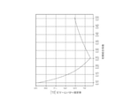
上部クラッド層2-222の厚さは、行内の試料ウェルによって受け取られる強度の均一性の程度に対し影響し得る。図2-2および図2-3は、上部クラッド厚さが変化され、非直線的なテーパを有する導波路が、1024個の試料ウェルの行について最小の相対強度を達成するように設計される、シミュレーション結果を示す。導波路は、120nmの厚さ、300nmの最小幅値、および1300nmの最大幅値を有する。試料ウェルは、300nmの深さを有する。図2-2は、1024個のすべての試料ウェルにわたる最小相対強度を達成するために必要とされる導波路へのパワー入力と、上部クラッド厚さのグラフを示す。図2-2に示されるグラフは、導波路への入力パワーが最小である、380nmと400nmの間の上部クラッド層2-222の厚さの最適値がどのように存在するかを示す。図2-3は、試料ウェルの行に沿った強度の不均一性の量と、上部クラッド厚さのグラフを示し、ここで、不均一性は、試料ウェルにおける最低強度に対する試料ウェルにおける最高強度の比に対応している。1に等しい不均一性値は、最高強度値と最低強度値が等しく、したがって、行内のすべての試料ウェルにおいて均一な強度が存在するシナリオに対応する。図2-2と図2-3との両方を参照すると、入力パワー、上部クラッド厚さ、および不均一性の間にバランスが存在する。特に、上部クラッド層がその最適値よりも厚いとき、1に等しい不均一性が達成され得るが、上部クラッド厚さがその最適値である場合よりも入力パワーが高い。 The thickness of the upper clad layer 2-222 can affect the degree of intensity uniformity received by the sample wells in the row. 2-2 and 2-3 are designed so that a waveguide with varying top clad thickness and a non-linear taper achieves the minimum relative strength for a row of 1024 sample wells. , The simulation result is shown. The waveguide has a thickness of 120 nm, a minimum width value of 300 nm, and a maximum width value of 1300 nm. The sample well has a depth of 300 nm. Figure 2-2 shows a graph of the power input to the waveguide and the top clad thickness required to achieve the minimum relative strength across all 1024 sample wells. The graph shown in FIG. 2-2 shows how there is an optimum thickness of the top clad layer 2-222 between 380 nm and 400 nm where the input power to the waveguide is minimal. FIG. 2-3 shows a graph of the amount of intensity non-uniformity along the rows of the sample well and the top clad thickness, where the non-uniformity is the highest strength in the sample well relative to the lowest strength in the sample well. Corresponds to the ratio of. A non-uniformity value equal to 1 corresponds to a scenario where the highest and lowest intensity values are equal and therefore uniform intensities exist for all sample wells in the row. With reference to both FIGS. 2-2 and 2-3, there is a balance between input power, top clad thickness, and non-uniformity. In particular, when the upper clad layer is thicker than its optimum value, non-uniformity equal to 1 can be achieved, but the input power is higher than when the upper clad thickness is its optimum value.
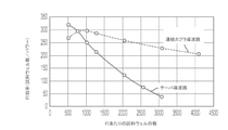
図2-4、図2-5、および図2-6は、395nmの上部クラッド厚さ層を有する1024個の試料ウェルの行に関して構成されたテーパ導波路についてのシミュレーション結果を示す。図2-4は、相対強度と、試料ウェル数のグラフであり、どのように個々の試料ウェルにおける相対強度がすべての試料ウェルにわたって均一であるかを示す。図2-5は、導波路におけるパワーと、行内の試料ウェル数のグラフであり、どのように光パワーが試料ウェルの行に沿って減少するかを示す。図2-6は、導波路幅と、行内の試料ウェル数のグラフであり、図2-4に示された均一な強度を得るために使用される導波路のテーパ・プロファイルを示す。 2-4, 2-5, and 2-6 show simulation results for tapered waveguides configured for rows of 1024 sample wells with a 395 nm top clad thickness layer. FIG. 2-4 is a graph of relative strength and number of sample wells, showing how the relative strength in individual sample wells is uniform across all sample wells. FIG. 2-5 is a graph of the power in the waveguide and the number of sample wells in a row, showing how the optical power decreases along the row of sample wells. FIG. 2-6 is a graph of waveguide width and number of sample wells in a row, showing the taper profile of the waveguide used to obtain the uniform strength shown in FIG. 2-4.
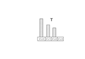
導波路の長さおよび行内の試料ウェルの数は、行の試料ウェル間に分布する強度の均一性に影響し得る追加パラメータである。図2-7および図2-8は、行内の異なる数の試料ウェルに対して均一な強度を有するように設計されたテーパ導波路についてのシミュレーション結果を示す。具体的には、図2-7は、導波路へのパワー入力と、行あたりの試料ウェルの数のグラフであり、図2-8は、単位パワーあたりのセンサの数に対応する行効率と、行あたりの試料ウェルの数のグラフである。図2-7に示されるように、入力パワーは、行内の試料ウェルの数が増加するにつれて増大する。図2-8は、行内の試料ウェルの数が増加するにつれて効率がどのように低下するかを示す。 The length of the waveguide and the number of sample wells in the row are additional parameters that can affect the uniformity of the intensity distributed between the sample wells in the row. 2-7 and 2-8 show simulation results for tapered waveguides designed to have uniform strength for different numbers of sample wells in a row. Specifically, FIG. 2-7 is a graph of the power input to the waveguide and the number of sample wells per row, and FIG. 2-8 is the row efficiency corresponding to the number of sensors per unit power. , Is a graph of the number of sample wells per row. As shown in Figure 2-7, the input power increases as the number of sample wells in the row increases. FIG. 2-8 shows how efficiency decreases as the number of sample wells in a row increases.
集積デバイスにおけるテーパ導波路の使用は、実質的に均一な様式で試料ウェル間に励起光を送達する上でいくつかの利点を提供し得るが、試料ウェルの数を増加させることにより集積デバイスがスケール変更されるときにテーパ導波路を使用するには制限があり得る。図2-7および図2-8に関連して論じられるように、行内の試料ウェルの数が増加するにつれて、導波路へのより多くのパワー入力が必要とされ、行効率が低下する。本発明者らは、複数の導波路を使用して試料ウェルの行と結合することにより、1つのテーパ導波路のみを使用することに関連するそのような制限を克服できることを認識して理解した。複数の導波路を使用することにより、単一のテーパ導波路を使用して達成される場合よりも長い行の試料ウェルが実質的に均一な強度を有することが可能になり得る。したがって、いくつかの実施形態は、試料ウェルの行と光学的に結合するように構成された複数の導波路を有する集積デバイスに関する。これらの構成は、いくつかの実施形態によれば、テーパ導波路と組み合わせて使用され得る。そのような実施形態では、試料ウェルの単一行と光学的に結合する複数の導波路は、少なくとも導波路が行内の試料ウェルの一部と結合する領域内でテーパ状にされ得る。そのような構成は、単一の導波路が使用された場合よりも多数の試料ウェルを有する行が、同様の強度を受けることを可能にし得る。 The use of tapered waveguides in integrated devices can provide several advantages in delivering excitation light between sample wells in a substantially uniform manner, but by increasing the number of sample wells the integrated device There may be restrictions on the use of tapered waveguides when scaled. As discussed in connection with FIGS. 2-7 and 2-8, as the number of sample wells in a row increases, more power input to the waveguide is required and row efficiency decreases. We have recognized and understood that by using multiple waveguides to couple with rows of sample wells, such limitations associated with using only one tapered waveguide can be overcome. .. The use of multiple waveguides may allow sample wells in longer rows to have substantially uniform strength than would be achieved using a single tapered waveguide. Accordingly, some embodiments relate to an integrated device having a plurality of waveguides configured to optically couple with a row of sample wells. These configurations can be used in combination with tapered waveguides, according to some embodiments. In such an embodiment, the plurality of waveguides optically coupled to a single row of sample wells can be tapered, at least within the region where the waveguide couples with a portion of the sample wells within the row. Such a configuration may allow rows with more sample wells to receive similar intensities than if a single waveguide was used.
集積デバイスのいくつかの実施形態では、第1の導波路は、行内の試料ウェルの第1のグループと光学的に結合するように配置され、第2の導波路は、行内の試料ウェルの第2のグループと光学的に結合するように配置される。試料ウェルの第1のグループと第2のグループとの間で、第1および第2の導波路は試料ウェルの行に関して配置がシフトされてよい。そのような構成は、試料ウェルの第1のグループと第2のグループとの間に導波路「行シフト」を有するとみなされてよい。行シフトの位置は、試料ウェルの行と第1の導波路の結合効率、または第1の導波路内を伝播するパワーが、特定の量まで低下して、デバイスの性能が影響を受ける場合に対応し得る。第2の導波路を使用して行内の後続の試料ウェルへの光の送達を続けることにより、第1の導波路のみを使用するこれらの制限が取り除かれる。追加の導波路が、同じ行内の追加のグループの試料ウェルと光学的に結合するように含まれ配置されてもよい。この導波路構成は、試料ウェル・アレイにおける他の行に実装されてもよく、たとえば、個々の行における試料ウェルの数を増加させることによって、アレイ内の試料ウェルの数を増加させるように使用され得る。 In some embodiments of the integrated device, the first waveguide is arranged to optically couple with the first group of sample wells in the row, and the second waveguide is the second of the sample wells in the row. Arranged so as to optically couple with the two groups. The arrangement of the first and second waveguides may be shifted with respect to the rows of the sample wells between the first and second groups of sample wells. Such a configuration may be considered to have a waveguide "row shift" between the first and second groups of sample wells. The position of the row shift is when the coupling efficiency between the row of the sample well and the first waveguide, or the power propagating in the first waveguide, drops to a certain amount, affecting the performance of the device. Can be accommodated. By continuing to deliver light to subsequent sample wells in the row using the second waveguide, these limitations of using only the first waveguide are removed. Additional waveguides may be included and arranged to optically couple with additional groups of sample wells in the same row. This waveguide configuration may be implemented in other rows of the sample well array, for example used to increase the number of sample wells in the array by increasing the number of sample wells in each row. Can be done.
図3-1は、複数の導波路が試料ウェルの個々の行に対して光を送達するために使用される、行シフト導波路構成を示す集積デバイスの平面図である。導波路への光入力の方向は矢印で示され、z方向である。図3-1は、試料ウェル3-108a、3-108b、および3-108cを有する行、ならびに試料ウェル3-108d、3-108e、および3-108fを有する行を含む、試料ウェルの3つの行を示しており、3つの導波路が、行内の3つの異なるグループの試料ウェルと光学的に結合する(たとえば、エバネッセント結合する)ように配置されている。たとえば、導波路3-220aが試料ウェル3-108aと光学的に結合するように配置され、導波路3-220bが試料ウェル3-108cと光学的に結合するように配置される。別の例として、導波路3-220dが試料ウェル3-108dと光学的に結合するように配置され、一方、導波路3-220eが試料ウェル3-108fと光学的に結合するように配置される。導波路の光結合は、試料ウェルが導波路に沿って伝播する光モードの一部を受け取るのに適した距離で、たとえば図1-1の導波路1-220によって示されるように、導波路が試料ウェルの下に配置されるエバネッセント結合を介して生じ得る。いくつかの実施形態によれば、導波路3-220aは、試料ウェル3-108aおよび領域3-110内の同じ行内の他の試料ウェルとエバネッセント結合するように配置されてよく、導波路3-220bは、試料ウェル3-108cおよび領域3-114内の同じ行内の他の試料ウェルとエバネッセント結合するように配置されてよい。追加の導波路が、同じ行内の後続の試料ウェルに光を送達するのに使用されてもよい。たとえば、図3-1は、図3-1に示される図に存在しない追加の試料ウェルと結合し得る導波路3-220cおよび3-220fを示す。具体的には、領域3-114に続く追加の行シフト領域の後、導波路3-220cは、試料ウェル3-108cと同じ行内の試料ウェルと結合することができ、導波路3-220eは、試料ウェル3-108fと同じ行内の試料ウェルと結合することができる。 FIG. 3-1 is a plan view of an integrated device showing a row-shifted waveguide configuration in which multiple waveguides are used to deliver light to individual rows of sample wells. The direction of the optical input to the waveguide is indicated by an arrow and is the z direction. FIG. 3-1 shows three sample wells, including a row with sample wells 3-108a, 3-108b, and 3-108c, and a row with sample wells 3-108d, 3-108e, and 3-108f. The rows are shown and the three waveguides are arranged to optically bond (eg, evanescently bond) to three different groups of sample wells within the row. For example, the waveguide 3-220a is arranged to optically couple with the sample well 3-108a and the waveguide 3-220b is arranged to optically couple with the sample well 3-108c. As another example, the waveguide 3-220d is arranged to optically couple with the sample well 3-108d, while the waveguide 3-220e is arranged to optically couple with the sample well 3-108f. Ru. The optical coupling of the waveguide is a suitable distance for the sample well to receive part of the optical mode propagating along the waveguide, for example, as shown by waveguide 1-220 in FIG. 1-1. Can occur via an evanescent bond placed beneath the sample well. According to some embodiments, the waveguide 3-220a may be arranged to evanescently couple with the sample well 3-108a and other sample wells in the same row within the region 3-110, the waveguide 3-. The 220b may be arranged to evanescently bind to the sample well 3-108c and other sample wells in the same row within region 3-114. Additional waveguides may be used to deliver light to subsequent sample wells within the same row. For example, FIG. 3-1 shows waveguides 3-220c and 3-220f that can be coupled to additional sample wells not present in the figure shown in FIG. 3-1. Specifically, after an additional row shift region following region 3-114, the waveguide 3-220c can be coupled to a sample well in the same row as the sample well 3-108c, and the waveguide 3-220e , Can be combined with a sample well in the same row as the sample well 3-108f.
同じ行内の試料ウェルは、共通の軸に沿って実質的に整列された試料ウェルに対応し得る。特定の行について、領域3-110内の試料ウェルのグループが軸に沿って実質的に整列され得る。図3-1に示されるように、試料ウェル3-108a、3-108b、および3-108cは軸(z方向の)に沿って整列され、同じ行にあるとみなされる。導波路は、軸に対して配置され得る。いくつかの実施形態では、試料ウェルのグループと結合するように構成された導波路の一部分が、軸と実質的に平行であってよく、複数の導波路が、異なるグループの試料ウェルと光学的に結合し、試料ウェルの行に沿った異なる部分で軸に実質的に平行であってよい。図3-1に示されるように、導波路3-220aは、領域3-110内で試料ウェル3-108a、3-108b、および3-108cに沿って軸に実質的に平行であり、導波路3-220bは領域3-114内で軸に実質的に平行である。 Sample wells within the same row may correspond to sample wells that are substantially aligned along a common axis. For a particular row, a group of sample wells within region 3-110 can be substantially aligned along the axis. As shown in FIG. 3-1 the sample wells 3-108a, 3-108b, and 3-108c are aligned along the axis (in the z direction) and are considered to be in the same row. The waveguide can be located with respect to the axis. In some embodiments, a portion of the waveguide configured to couple with a group of sample wells may be substantially parallel to the axis, and the plurality of waveguides may be optically with different groups of sample wells. And may be substantially parallel to the axis at different portions along the row of the sample well. As shown in FIG. 3-1 the waveguide 3-220a is substantially parallel to the axis along the sample wells 3-108a, 3-108b, and 3-108c within the region 3-110 and leads. Waveguide 3-220b is substantially parallel to the axis within region 3-114.
導波路間の間隔は、導波路が互いに効果的に光学的に分離されるような間隔であり得る。いくつかの実施形態では、エバネッセント結合が2つの導波路間にないかまたはほとんどないように、一方の導波路が他方の導波路から分離され得る。いくつかの実施形態では、2つの導波路間の横方向距離は、導波路が有するように構成された光モード・サイズに依存し得る。 The spacing between the waveguides can be such that the waveguides are effectively optically separated from each other. In some embodiments, one waveguide may be separated from the other, such that there is little or no evanescent coupling between the two waveguides. In some embodiments, the lateral distance between the two waveguides may depend on the optical mode size configured for the waveguide.
図3-1に示された導波路構成は、領域3-110、3-112、および3-114を有する。領域3-110は、導波路3-220aなどの第1の導波路が、試料ウェル3-108aなどの行内の試料ウェルの第1のグループと光学的に結合し、光を試料ウェルの第1のグループに対し送達する場所である。領域3-114は、導波路3-220bなどの第2の導波路が、試料ウェル3-108cなどの行内の試料ウェルの第2のグループと光学的に結合し、光を試料ウェルの第2のグループに対し送達する場所である。領域3-112は、第1導波路と第2導波路との間の行シフトが発生する場所に対応する。図3-1に示されるように、行シフト構成は、第1の導波路が行内の試料ウェルと光学的に結合するように配置されずに、第2の導波路が行内の試料ウェルと光学的に結合するように配置されるように導波路を湾曲させることを含む。行シフト構成は、第1の導波路と領域3-110内の試料ウェルとの間の距離が、第1の導波路と領域3-112内の試料ウェルとの間の距離よりも小さいという結果をもたらす。さらに、行シフト構成は、第2の導波路と領域3-114内の試料ウェルとの間の距離が、第2の導波路と領域3-112内の試料ウェルとの間の距離よりも小さいという結果をもたらす。たとえば、導波路3-220aおよび3-220dは、領域3-112において湾曲して試料ウェルのそれぞれの行から(x方向に沿って)オフセットされ、オフセットは、導波路を通る光伝播の方向に沿って増大する。さらに、導波路3-220bおよび3-220eは、領域3-112において湾曲させられ、試料ウェルのそれぞれの行から(x方向に沿って)オフセットされるが、オフセットは、導波路を通る光伝播の方向に沿って減少し、導波路3-220bおよび3-220eを試料ウェル行により近接して配置する。領域3-112における行シフト・プロファイルは、任意の適切なプロファイルおよび/または長さを有してよい。図3-1に示された導波路は、領域3-112で同様の行シフト・プロファイルを有するが、いくつかの実施形態は、領域3-112内で異なるプロファイルを有する同じ行に結合する導波路を含んでよいことが理解される。 The waveguide configuration shown in FIG. 3-1 has regions 3-110, 3-112, and 3-114. In region 3-110, a first waveguide, such as waveguide 3-220a, optically couples with a first group of sample wells in a row, such as sample well 3-108a, to direct light to the first group of sample wells. The place of delivery to the group of. In region 3-114, a second waveguide, such as waveguide 3-220b, optically couples with a second group of sample wells in a row, such as sample well 3-108c, to direct light to the second group of sample wells. The place of delivery to the group of. Region 3-112 corresponds to where a row shift occurs between the first and second waveguides. As shown in FIG. 3-1 in the row shift configuration, the first waveguide is not arranged to optically couple with the sample well in the row, and the second waveguide is optically coupled to the sample well in the row. Includes bending the waveguide so that it is arranged so as to be coupled. The row shift configuration results in the distance between the first waveguide and the sample well in region 3-110 being smaller than the distance between the first waveguide and the sample well in region 3-112. Bring. Further, in the row shift configuration, the distance between the second waveguide and the sample well in region 3-114 is smaller than the distance between the second waveguide and the sample well in region 3-112. The result is that. For example, the waveguides 3-220a and 3-220d are curved in region 3-112 and offset from each row of sample wells (along the x direction), with the offset in the direction of light propagation through the waveguide. Increase along. Further, the waveguides 3-220b and 3-220e are curved in region 3-112 and offset (along the x direction) from each row of the sample well, but the offset is light propagation through the waveguide. The waveguides 3-220b and 3-220e are placed closer to the sample well row, decreasing along the direction of. The row shift profile in regions 3-112 may have any suitable profile and / or length. The waveguide shown in FIG. 3-1 has a similar row shift profile in region 3-112, but in some embodiments, leads to join to the same row with different profiles within region 3-112. It is understood that the waveguide may be included.
いくつかの実施形態では、行内の試料ウェルと光学的に結合するように構成された導波路の領域が、本願明細書に記載の技術を使用するなどして、その領域で導波路が結合する試料ウェルのグループについて実質的に均一な強度を達成するようにテーパ状にされ得る。図3-1に示されるように、導波路3-220aは領域3-110内でテーパ状にされ、導波路3-220bは領域3-114でテーパ状にされている。 In some embodiments, a region of the waveguide configured to optically couple with a sample well in a row is coupled in that region, such as by using the techniques described herein. It can be tapered to achieve substantially uniform strength for a group of sample wells. As shown in FIG. 3-1 the waveguide 3-220a is tapered in the region 3-110 and the waveguide 3-220b is tapered in the region 3-114.
集積デバイスは、個々の導波路へと入力パワーを提供するために1つまたは複数の光学部品(たとえば、図1-1に示されるルーティング領域1-202内に位置する光学スプリッタ)を備えることができる。いくつかの実施形態では、入力パワーは、すべての導波路にわたり実質的に同一であってよい。本発明者らは、行内の試料ウェルのグループと光学的に結合されていない導波路が、光がこの領域を通って伝播するとき、いくらかの光損失を受ける可能性があることを認識して理解した。そのため、いくつかの実施形態は、導波路がそれぞれの試料ウェルに光学的に結合する領域において導波路の1つまたは複数の特性を変化させることによって、そのような光損失を低減する構成を有することがある。たとえば、領域3-110内の導波路3-220bの一部分は、光損失を低減するための構成を有することができるが、導波路3-220bが領域3-114内の試料ウェルに光学的に結合する場合、導波路3-220aが領域3-110内の試料ウェルに光学的に結合する場合よりも少ない量のパワーを送達し得る。したがって、光を試料ウェルの行に送達する導波路のテーパは、導波路が試料ウェルに結合するために使用されるときの光パワーのこの変動に対処するために異なることがある。いくつかの実施形態では、領域3-110における第1の導波路のテーパ部分の長さは、領域3-114における第2の導波路のテーパ部分の長さとは異なることがある。テーパ部分の長さは、特定の導波路を使用して導波路のテーパ領域において光が送達される試料ウェルの数に対応してよい。いくつかの実施形態では、領域3-114における第2の導波路のテーパ部分の長さは、領域3-110における第1の導波路のテーパ部分の長さより短くてよい。そのような構成は、領域3-114において、領域3-110における第1の導波路よりも低い光パワーを有する第2の導波路を考慮し得る。たとえば、図3-1は、導波路3-220aのテーパ部分の長さに対応し得る6つの試料ウェルと結合する領域3-110内の導波路3-220aのテーパ部分を示し、領域3-114内の導波路3-220bのテーパ部分は5つの試料ウェルと結合するように示されている。第1および第2の導波路のテーパ部分は、図3-1に示されるよりも多いまたは少ない試料ウェルと結合し得ることが理解される。 The integrated device may include one or more optical components (eg, optical splitters located within routing regions 1-22 shown in FIG. 1-1) to provide input power to individual waveguides. can. In some embodiments, the input power may be substantially the same across all waveguides. We recognize that a waveguide that is not optically coupled to a group of sample wells in a row can suffer some photoloss as light propagates through this region. got it. As such, some embodiments have configurations that reduce such light loss by altering the properties of one or more of the waveguides in the region where the waveguide optically couples to each sample well. Sometimes. For example, a portion of the waveguide 3-220b in the region 3-110 may have a configuration for reducing light loss, but the waveguide 3-220b optically in the sample well in the region 3-114. When coupled, the waveguide 3-220a may deliver less power than when optically coupled to the sample wells in region 3-110. Therefore, the taper of the waveguide that delivers the light to the row of the sample well may differ to accommodate this variation in optical power as the waveguide is used to couple to the sample well. In some embodiments, the length of the tapered portion of the first waveguide in region 3-110 may differ from the length of the tapered portion of the second waveguide in region 3-114. The length of the tapered portion may correspond to the number of sample wells to which light is delivered in the tapered region of the waveguide using a particular waveguide. In some embodiments, the length of the tapered portion of the second waveguide in region 3-114 may be shorter than the length of the tapered portion of the first waveguide in region 3-110. Such a configuration may consider a second waveguide in region 3-114, which has a lower optical power than the first waveguide in region 3-110. For example, FIG. 3-1 shows the tapered portion of the waveguide 3-220a within the region 3-110 coupled to the six sample wells that may correspond to the length of the tapered portion of the waveguide 3-220a. The tapered portion of the waveguide 3-220b in 114 is shown to couple with five sample wells. It is understood that the tapered portions of the first and second waveguides can be coupled with more or less sample wells than shown in FIG. 3-1.
いくつかの実施形態では、導波路の行シフトが発生する場所に位置する行内の試料ウェルは、導波路と光学的に結合しないか、または行内の他の試料ウェルと比較して導波路との光結合の量が少ないことがある。したがって、試料ウェル・アレイの行シフト領域内に位置する試料ウェルは、より少ない量の光学パワーを受け取ることがある。試料の分析を行う集積デバイスの動作中、これらの試料ウェルは分析の結果から除外されてよく、なぜならば、これらの試料ウェルによって得られた結果の質が、所望の量の光(たとえば、特定の強度)で試料を照射するために不十分な能力によって影響を受ける可能性があるからである。図3-1に示されるように、領域3-112内の試料ウェルのグループは、同じ行の領域3-110内の試料ウェルまたは3-114内の試料ウェルよりも少ない光学パワーを受け取る可能性がある。これは、領域3-112に配置された試料ウェルが、その行の対応する第1または第2の導波路と光学的に結合しないかまたは所望の効率で光学的に結合しない可能性があるからである。たとえば、領域3-112は、試料ウェル3-108bを含み、試料ウェル3-108bは、導波路3-220aおよび3-220bの両方からオフセットされているため、領域3-110および3-114内の試料ウェル3-108aおよび3-108cなどの試料ウェルと比較して少ない量の光学パワーを受け取る可能性がある。同様に、領域3-112は、試料ウェル3-108dおよび3-108fと比較して少ない量の光学パワーを受け取る可能性がある試料ウェル3-108eを含む。したがって、集積デバイスの動作中に試料ウェル3-108bおよび3-108eを使用して得られたデータは、全体的な結果から除外されてよい。 In some embodiments, the sample well in the row located where the line shift of the waveguide occurs does not optically couple with the waveguide or is relative to the other sample well in the line. The amount of optical coupling may be small. Therefore, a sample well located within the row shift region of the sample well array may receive a smaller amount of optical power. During the operation of the integrated device performing the analysis of the samples, these sample wells may be excluded from the results of the analysis, because the quality of the results obtained by these sample wells is specified by the desired amount of light (eg, specific). This is because it may be affected by insufficient ability to irradiate the sample with (intensity). As shown in FIG. 3-1 a group of sample wells within region 3-112 may receive less optical power than a sample well within region 3-110 or 3-114 in the same row. There is. This is because the sample wells located in region 3-112 may not optically couple with the corresponding first or second waveguide in that row or with the desired efficiency. Is. For example, region 3-112 contains sample wells 3-108b, and sample wells 3-108b are offset from both waveguides 3-220a and 3-220b, so that they are within regions 3-110 and 3-114. It is possible to receive a smaller amount of optical power compared to sample wells such as sample wells 3-108a and 3-108c. Similarly, region 3-112 contains sample wells 3-108e, which may receive a smaller amount of optical power compared to sample wells 3-108d and 3-108f. Therefore, data obtained using sample wells 3-108b and 3-108e during the operation of the integrated device may be excluded from the overall results.
図3-1に示されるような行シフト構成を有する導波路アレイは、本願明細書に記載される1つまたは複数の他の構成要素と組み合わせて集積デバイス内に実装されてよい。いくつかの実施形態では、行シフト導波路構成を有する集積デバイスが、集積デバイスの表面から光を受け取り、導波路と光学的に結合するように構成された格子カプラを備えることができる。図3-1の文脈では、格子カプラは左側(負のz方向)に配置され、図3-1に示される矢印の方向に光を提供することができる。いくつかの実施形態では、行シフト導波路構成を有する集積デバイスは、1つまたは複数の光検出器と同じピクセルにおける試料ウェルから放出された光を受け取るように構成された1つまたは複数の光検出器を備えることができる。たとえば、試料ウェル3-108aを有するピクセルは、試料ウェル3-108aから放出される光を受け取るように配置および構成された1つまたは複数の光検出器を備えることができる。ピクセルは、図1-1のピクセル1-112によって示されるような断面構成を有してよい。 A waveguide array having a row shift configuration as shown in FIG. 3-1 may be implemented in an integrated device in combination with one or more of the other components described herein. In some embodiments, an integrated device with a rowshift waveguide configuration can include a grid coupler configured to receive light from the surface of the integrated device and optically couple with the waveguide. In the context of FIG. 3-1 the grid coupler is located on the left side (negative z direction) and can provide light in the direction of the arrow shown in FIG. 3-1. In some embodiments, an integrated device with a rowshift waveguide configuration is configured to receive light emitted from a sample well at the same pixel as one or more photodetectors. It can be equipped with a detector. For example, a pixel with sample well 3-108a may include one or more photodetectors arranged and configured to receive light emitted from sample well 3-108a. The pixels may have a cross-sectional configuration as shown by pixels 1-112 in FIG. 1-1.
試料ウェルの行ごとの導波路であって、光パワー源として作用し、行内の試料ウェルと光学的に結合するように配置された1つまたは複数の他の導波路に光学的に結合する導波路を有するアレイ導波路構成がいくつかの利点を提供し得ることを、本発明者らは認識して理解した。光パワー源として作用する導波路は、「パワー導波路」とみなされ得る。そのような構成の利点の1つは、アレイ導波路の全体的なフットプリントが低減され得ることであり、これは、試料ウェルの行間の距離が小さく、試料ウェルの行間に配置された複数の導波路を収容しない集積デバイスを構成する際の利点を提供し得る。そのため、集積デバイスのいくつかの実施形態は、試料ウェル・アレイの個々の行に関連付けられたパワー導波路、ならびに対応する行における1つまたは複数のパワー導波路および試料ウェルと光学的に結合する1つまたは複数の導波路を備えることがある。いくつかの実施形態では、1つまたは複数の他の導波路が、光スプリッタ(たとえば、方向性カプラ)を介してパワー導波路と光学的に結合することができる。いくつかの実施形態では、試料ウェルの行は、行に関連付けられたパワー導波路と光学的に結合し、行内の試料ウェルと光学的に結合する連続カプラの役割をする、導波路を有する。 A row-by-row waveguide of sample wells that acts as an optical power source and optically couples to one or more other waveguides arranged to optically couple to the sample wells in the row. We have recognized and understood that array waveguide configurations with waveguides can provide several advantages. A waveguide that acts as an optical power source can be considered a "power waveguide". One of the advantages of such a configuration is that the overall footprint of the array waveguide can be reduced, which means that the distance between the rows of the sample wells is small and multiple rows of sample wells are located. It may provide advantages in configuring an integrated device that does not accommodate a waveguide. As such, some embodiments of the integrated device are optically coupled to the power waveguides associated with the individual rows of the sample well array, as well as one or more power waveguides and sample wells in the corresponding rows. It may have one or more waveguides. In some embodiments, one or more other waveguides can be optically coupled to the power waveguide via an optical splitter (eg, a directional coupler). In some embodiments, the row of sample wells has a waveguide that acts as a continuous coupler that optically coupled to the power waveguide associated with the row and optically coupled to the sample wells within the row.
図3-2は、アレイ導波路構成を有する集積デバイスの平面図であり、アレイ導波路構成は、試料ウェルの行について、パワー導波路と、行内の試料ウェルの異なるグループと光学的に結合するように配置された複数の導波路とを備える。試料ウェル3-208aおよび3-208bは、同じ行内にあり、導波路3-230aは、その行のパワー導波路の役割をする。同様に、試料ウェル3-208cおよび3-208dは、異なる1つの行内にあり、導波路3-230bは、その行のパワー導波路の役割をする。パワー導波路に沿った光伝播の方向が図3-2における矢印で示される。パワー導波路に沿って、個々の導波路はパワー導波路と結合し、行内の試料ウェルのグループと光学的に結合するように配置される。図3-2では、導波路3-240aおよび3-240bは、パワー導波路3-230aと光学的に結合し、試料ウェル3-208aおよび3-208bを有する行における試料ウェルに光を送達するように構成される。いくつかの実施形態では、導波路3-240aおよび3-240bは、本願明細書に記載のテーパ導波路を使用するなどして、これらの導波路と光学的に結合する試料ウェルに対して実質的に均一な強度を提供するようにテーパ状にされる。図3-2に示されるように、試料ウェル3-208aは、試料ウェル3-208bが光学的に結合する導波路3-240aの領域よりも広い幅を有する導波路3-240aの領域と光学的に結合するように構成される。同様に、試料ウェル3-208fは、試料ウェル3-208gが光学的に結合する導波路3-240bの領域よりも広い幅を有する導波路3-240bの領域と光学的に結合するように構成される。また、試料ウェル3-208aおよび3-208bと異なる行にある試料ウェル3-208cおよび3-208dは、異なる幅を有する導波路3-240cの異なる領域と光学的に結合するように構成される。具体的には、試料ウェル3-208cは、試料ウェル3-208dが光学的に結合する導波路3-240cの領域よりも広い幅を有する導波路3-240cの領域と光学的に結合するように構成される。 FIG. 3-2 is a plan view of an integrated device with an array waveguide configuration in which the array waveguide configuration optically couples a row of sample wells with a power waveguide and different groups of sample wells within the row. It is provided with a plurality of waveguides arranged in such a manner. The sample wells 3-208a and 3-208b are in the same row, and the waveguide 3-230a acts as a power waveguide in that row. Similarly, the sample wells 3-208c and 3-208d are in different rows, and the waveguide 3-230b acts as a power waveguide for that row. The direction of light propagation along the power waveguide is indicated by the arrow in Figure 3-2. Along the power waveguide, the individual waveguides are arranged to couple with the power waveguide and optically couple with a group of sample wells in the row. In FIG. 3-2, the waveguides 3-240a and 3-240b optically couple with the power waveguide 3-230a to deliver light to the sample wells in the row having the sample wells 3-208a and 3-208b. It is configured as follows. In some embodiments, the waveguides 3-240a and 3-240b are substantially relative to the sample wells optically coupled to these waveguides, such as by using the tapered waveguides described herein. It is tapered to provide uniform strength. As shown in FIG. 3-2, the sample well 3-208a is optically with the region of the waveguide 3-240a having a wider width than the region of the waveguide 3-240a to which the sample well 3-208b is optically coupled. It is configured to be combined. Similarly, the sample well 3-208f is configured to optically couple to a region of the waveguide 3-240b that has a wider width than the region of the waveguide 3-240b to which the sample well 3-208g is optically coupled. Will be done. Also, the sample wells 3-208c and 3-208d in different rows from the sample wells 3-208a and 3-208b are configured to optically couple to different regions of the waveguide 3-240c having different widths. .. Specifically, the sample well 3-208c is optically coupled to a region of the waveguide 3-240c that has a wider width than the region of the waveguide 3-240c to which the sample well 3-208d is optically coupled. It is composed of.
パワー導波路3-230aおよび3-230bは、導波路の長さに沿って実質的に均一な幅を有することなどによって、光が導波路に沿って伝播するときの光損失を低減する構成を有することができる。図3-2に示されるように、導波路3-240aおよび3-240bは、それぞれパワー・スプリッタ3-250aおよび3-250bを介して、パワー導波路3-230aと光学的に結合することができる。さらに、導波路3-240cおよび3-240dは、1つまたは複数のパワー・スプリッタを介してパワー導波路3-230bと光学的に結合することができる。適切なパワー・スプリッタの例は、方向性カプラ、多モード干渉スプリッタ、または任意の他の適切なパワー分割光学部品を含む。方向性カプラがパワー・スプリッタとして使用される実施形態では、方向性カプラの構成は、試料ウェルのグループと光学的に結合する導波路へと入力される所望の相対量の光パワーを達成するために、特定のパワー分割比で構成され得る。 The power waveguides 3-230a and 3-230b are configured to reduce light loss when light propagates along the waveguide by having a substantially uniform width along the length of the waveguide. Can have. As shown in FIG. 3-2, the waveguides 3-240a and 3-240b can be optically coupled to the power waveguide 3-230a via the power splitters 3-250a and 3-250b, respectively. can. Further, the waveguides 3-240c and 3-240d can be optically coupled to the power waveguide 3-230b via one or more power splitters. Examples of suitable power splitters include directional couplers, multimode interference splitters, or any other suitable power split optics. In embodiments where the directional coupler is used as a power splitter, the directional coupler configuration is to achieve the desired relative amount of optical power input into the waveguide that optically couples with a group of sample wells. In addition, it may be configured with a specific power split ratio.
いくつかの実施形態では、パワー導波路と光学的に結合する個々のパワー・スプリッタは、同様の分割比を有することがある。図3-2を参照すると、パワー・スプリッタ3-250aおよびパワー・スプリッタ3-250bは、パワー導波路3-230aに対し同じ分割比を有することができる。そのような場合、パワー導波路3-230aがパワー・スプリッタ3-250bの前にパワー・スプリッタ3-250aと結合するので、導波路3-240bは、光が3-230aに沿って伝播するときに導波路3-240aよりも少ない光パワーを受け取るように構成される。そのような実施形態では、導波路3-240aおよび3-240bは、入力パワーの差に対応するために異なるテーパ形状を有することにより、導波路3-240aおよび3-240bと光学的に結合するように構成された試料ウェルが、実質的に同様の強度を受け取ることができ、したがって、導波路3-240aと3-240bの異なるテーパ形状は、パワー・スプリッタ3-250aおよび3-250bを介してパワー・スプリッタ3-230aから導波路3-240aおよび3-240bによって受け取られる光パワーの差を考慮し得る。たとえば、導波路3-240bは、パワー導波路3-230aからのより低い入力パワーを受け取ることを考慮して、導波路3-240aよりも短いテーパ長を有することができる。 In some embodiments, the individual power splitters optically coupled to the power waveguide may have similar split ratios. Referring to FIG. 3-2, the power splitter 3-250a and the power splitter 3-250b can have the same division ratio with respect to the power waveguide 3-230a. In such a case, the power waveguide 3-240b couples with the power splitter 3-250a before the power splitter 3-250b so that the waveguide 3-240b is when light propagates along 3-230a. Is configured to receive less optical power than the waveguide 3-240a. In such an embodiment, the waveguides 3-240a and 3-240b are optically coupled to the waveguides 3-240a and 3-240b by having different tapered shapes to accommodate the difference in input power. Sample wells configured in this way can receive substantially similar intensities, so that the different tapered shapes of the waveguides 3-240a and 3-240b are via the power splitters 3-250a and 3-250b. The difference in optical power received from the power splitter 3-230a by the waveguides 3-240a and 3-240b can be taken into account. For example, the waveguide 3-240b can have a shorter taper length than the waveguide 3-240a, taking into account the lower input power from the power waveguide 3-230a.
いくつかの実施形態では、パワー導波路と光学的に結合する個々のパワー・スプリッタは、試料ウェルと光学的に結合する導波路が実質的に同様の入力パワーを受け取るように、異なる分割比を有することができる。図3-2を参照すると、パワー・スプリッタ3-250aおよびパワー・スプリッタ3-250bは、同様の量の光パワーが導波路3-240aおよび3-240bに結合するように、パワー導波路3-230aと異なる分割比を有することができる。そのような実施形態では、導波路3-230aおよび3-230bは、同様のテーパ形状を有して、導波路3-230aおよび3-230bと光学的に結合する試料ウェルが実質的に同様の強度を受け取ることを可能にする。 In some embodiments, the individual power splitters optically coupled to the power waveguide have different split ratios so that the waveguide optically coupled to the sample well receives substantially similar input power. Can have. Referring to FIG. 3-2, the power splitter 3-250a and the power splitter 3-250b have a power waveguide 3-so that a similar amount of optical power is coupled to the waveguides 3-240a and 3-240b. It can have a split ratio different from that of 230a. In such an embodiment, the waveguides 3-230a and 3-230b have similar tapered shapes, and the sample wells optically coupled to the waveguides 3-230a and 3-230b are substantially similar. Allows you to receive strength.
いくつかの実施形態は、行内の試料ウェルに光学的に結合する個々の導波路間の遷移領域を含むことがある。遷移領域内に位置する試料ウェルは、遷移領域の外側の行内の他の試料ウェルと同様に、導波路のうちの1つと光学的に結合するように配置されず、または同様の量の光パワーを受け取るようには配置されない。図3-2に示されるように、試料ウェル3-208eは、導波路3-240aと3-240bとの間の遷移領域内に位置する試料ウェルの例である。試料ウェル3-208eは、試料ウェル3-208aおよび3-208bよりも少ない量の光パワーを受け取り得る。そのような場合、試料ウェル3-208eは、試料ウェル3-208aおよび3-208bなどの他の試料ウェルと比較して少ない量の励起光を受け取るので、試料ウェル3-208eを使用して得られた任意のデータは、分析から除外されることが可能である。 Some embodiments may include transition regions between individual waveguides that optically couple to sample wells within a row. A sample well located within the transition region, like the other sample wells in the row outside the transition region, is not arranged to optically couple with one of the waveguides, or has a similar amount of optical power. Is not placed to receive. As shown in FIG. 3-2, the sample well 3-208e is an example of a sample well located in the transition region between the waveguides 3-240a and 3-240b. The sample well 3-208e may receive less light power than the sample wells 3-208a and 3-208b. In such cases, sample wells 3-208e receive a smaller amount of excitation light compared to other sample wells such as sample wells 3-208a and 3-208b and can be obtained using sample wells 3-208e. Any data obtained can be excluded from the analysis.
いくつかの実施形態では、集積デバイスは、複数の行の試料ウェルに対し光パワーを送達するように構成されたパワー導波路を備えることができる。図3-3は、パワー導波路3-330aに隣接する試料ウェルの2つの行に光を送達するように構成されたパワー導波路3-330aを有する集積デバイスの平面図である。特に、パワー導波路3-330aは、試料ウェル3-308aおよび3-308bを含む試料ウェルの行、ならびに試料ウェル3-308cおよび3-308dを含む試料ウェルの行と光学的に結合するように構成される。図3-3に示す構成におけるように、これらの2つの行の試料ウェルは、導波路とパワー・スプリッタとの組み合わせを介してパワー導波路3-330aに光学的に結合することができる。導波路3-340aは、試料ウェル3-308aおよび3-308bと光学的に結合するように配置され、パワー・スプリッタを介してパワー導波路3-330aに光学的に結合することができる。導波路3-340bは、試料ウェル3-308cおよび3-308dと光学的に結合するように配置され、パワー・スプリッタを介してパワー導波路3-330aに光学的に結合することができる。図3-3に関連して説明された導波路およびパワー・スプリッタは、導波路3-340aおよび3-340b、ならびにこれらの導波路をパワー導波路3-330aに結合するために使用されるパワー・スプリッタに使用され得る。同様に、パワー導波路3-330bは、試料ウェル3-308eおよび3-308fを含む試料ウェルの行に対し、ならびに3-308gおよび3-308hを含む試料ウェルの行に対し光を送達するように構成される。特に、導波路3-340cは、パワー導波路3-330bおよび試料ウェル3-308eおよび3-308fと光学的に結合するように配置され、導波路3-340dは、パワー導波路3-330bおよび試料ウェル3-308gおよび3-308hと光学的に結合するように配置される。 In some embodiments, the integrated device can include a power waveguide configured to deliver optical power to multiple rows of sample wells. FIG. 3-3 is a plan view of an integrated device having a power waveguide 3-330a configured to deliver light to two rows of sample wells adjacent to the power waveguide 3-330a. In particular, the power waveguide 3-330a is to optically couple with a row of sample wells containing sample wells 3-308a and 3-308b and a row of sample wells containing sample wells 3-308c and 3-308d. It is composed. As in the configuration shown in FIG. 3-3, these two rows of sample wells can be optically coupled to the power waveguide 3-330a via a combination of a waveguide and a power splitter. The waveguide 3-340a is arranged to optically couple with the sample wells 3-308a and 3-308b and can be optically coupled to the power waveguide 3-330a via a power splitter. The waveguide 3-340b is arranged to optically couple with the sample wells 3-308c and 3-308d and can be optically coupled to the power waveguide 3-330a via a power splitter. The waveguides and power splitters described in connection with FIG. 3-3 are the waveguides 3-340a and 3-340b, as well as the power used to couple these waveguides to the power waveguide 3-330a. -Can be used for splitters. Similarly, the power waveguide 3-330b is intended to deliver light to a row of sample wells containing sample wells 3-308e and 3-308f, and to a row of sample wells containing 3-308g and 3-308h. It is composed of. In particular, the waveguide 3-340c is arranged to optically couple with the power waveguide 3-330b and the sample wells 3-308e and 3-308f, and the waveguide 3-340d is the power waveguide 3-330b and It is arranged so as to optically bond with the sample wells 3-308g and 3-308h.
いくつかの実施形態では、行内の試料ウェルと光学的に結合するように配置された導波路は、パワー導波路の端部を介するなどして、パワー導波路に接続され得る。たとえば、試料ウェルの行と光学的に結合するように構成された一連の導波路があり、光がパワー導波路を介して一連の導波路に光学的に結合される導波路構成において、パワー導波路の光入力端から離れたそうした導波路は、光接続を介するなどして、パワー導波路に直接接続され得る。そのような構成では、パワー導波路に沿って伝播する光は、光接続を介して伝播することによって導波路に送達され得る。図3-4は、パワー導波路3-430を有する導波路構成の平面図であり、矢印は、パワー導波路3-430への光入力の方向を示す。導波路3-440a、3-440b、3-440c、および3-440dは、試料ウェル3-408a、3-408b、3-408c、および3-408dを有する試料ウェルの行と光学的に結合するように構成される。導波路3-440a、3-440b、および3-440cは、それぞれパワー・スプリッタ3-450a、3-450b、および3-450cを介してパワー導波路3-430と光学的に結合する。導波路3-440dは光接続3-460を介してパワー導波路に接続される。光接続3-460は、パワー導波路3-430からの光出力を導波路3-440dに向けるための任意の適切なサイズおよび形状を有し得る。 In some embodiments, the waveguide arranged to optically couple with the sample wells in the row may be connected to the power waveguide, such as through the end of the power waveguide. For example, in a waveguide configuration in which there is a series of waveguides configured to optically couple with a row of sample wells, and light is optically coupled to the series of waveguides via a power waveguide, power conduction. Such a waveguide away from the optical input end of the waveguide may be directly connected to the power waveguide, such as via an optical connection. In such a configuration, light propagating along the power waveguide can be delivered to the waveguide by propagating through an optical connection. FIG. 3-4 is a plan view of the waveguide configuration having the power waveguide 3-430, and the arrows indicate the direction of the optical input to the power waveguide 3-430. Waveguides 3-440a, 3-440b, 3-440c, and 3-440d optically couple with a row of sample wells having sample wells 3-408a, 3-408b, 3-408c, and 3-408d. It is configured as follows. The waveguides 3-440a, 3-440b, and 3-440c are optically coupled to the power waveguide 3-430 via the power splitters 3-450a, 3-450b, and 3-450c, respectively. The waveguide 3-440d is connected to the power waveguide via an optical connection 3-460. The optical connection 3-460 may have any suitable size and shape for directing the optical output from the power waveguide 3-430 to the waveguide 3-440d.
いくつかの実施形態は、その長さに沿って変化する幅を有するパワー導波路を備えることができる。図3-4に示すように、パワー導波路3-430は、パワー導波路3-430がパワー・スプリッタ3-450a、3-450b、および3-450cと光学的に結合する領域において狭くなる幅を有する。パワー導波路3-430の幅は、パワー・スプリッタ3-450a、3-450b、および3-450cの間の領域において、パワー・スプリッタ3-450a、3-450b、および3-450cと重なる領域におけるよりも広い。 Some embodiments may comprise a power waveguide having a width that varies along its length. As shown in FIG. 3-4, the power waveguide 3-430 narrows in the region where the power waveguide 3-430 optically couples with the power splitters 3-450a, 3-450b, and 3-450c. Has. The width of the power waveguide 3-430 in the region between the power splitters 3-450a, 3-450b, and 3-450c overlaps with the power splitters 3-450a, 3-450b, and 3-450c. Wider than.
パワー導波路、パワー・スプリッタ、および特定の行内の試料ウェルに対し光学的に結合する導波路は、導波路構成を通って伝播する光が受ける光損失に対応するように適切に構成され得ることが理解される。例として、図3-4に示される導波路構成において、パワー・スプリッタ3-450a、3-450b、および3-450cはそれぞれ22%、30%、および48%のパワー分割比を有するように構成されてよい。パワー導波路3-430が個々の導波路3-440a、3-440b、3-440c、および3-440dの間に約10%のパワー損失を有する場合、行内のすべての試料ウェルを照射するのに必要とされるパワー導波路3-430に対する相対入力パワーは4.70である。導波路3-440a、3-440b、3-440c、および3-440dがそれぞれ512個の試料ウェルに光を送達するために使用される場合、入力パワーは約7.5a.u.(任意単位)である。そのような例では、単位パワーあたりの試料ウェルの数に対応する行効率は約273である。合計2048個の試料ウェル(4つの導波路のそれぞれについて512個の試料ウェル)を照射するためのこの構成は、2048個すべての試料を照射するために使用される単一のテーパ導波路を使用するのとは対照的である。単一のテーパ導波路構成では、テーパ導波路への入力パワーは約16.8a.u.であり、行効率は約122である。この例は、図3-4に示された構成が、どのように、必要な入力パワーを減少させながら試料ウェル・アレイ内の結合効率を増大し得るかを示す。 Powerguides, power splitters, and waveguides that optically couple to sample wells within a particular row can be adequately configured to accommodate the light loss incurred by light propagating through the waveguide configuration. Is understood. By way of example, in the waveguide configuration shown in FIG. 3-4, the power splitters 3-450a, 3-450b, and 3-450c are configured to have power split ratios of 22%, 30%, and 48%, respectively. May be done. If the power waveguide 3-430 has a power loss of about 10% between the individual waveguides 3-440a, 3-440b, 3-440c, and 3-440d, it illuminates all sample wells in the row. The relative input power to the power waveguide 3-430 required for is 4.70. When the waveguides 3-440a, 3-440b, 3-440c, and 3-440d are used to deliver light to 512 sample wells, respectively, the input power is about 7.5a. u. (Arbitrary unit). In such an example, the row efficiency corresponding to the number of sample wells per unit power is about 273. This configuration for irradiating a total of 2048 sample wells (512 sample wells for each of the four waveguides) uses a single tapered waveguide used to irradiate all 2048 samples. In contrast to doing. In a single tapered waveguide configuration, the input power to the tapered waveguide is approximately 16.8 a. u. The row efficiency is about 122. This example shows how the configuration shown in FIG. 3-4 can increase the coupling efficiency in the sample well array while reducing the required input power.
いくつかの実施形態は、パワー導波路の長さに沿って他の導波路と光学的に結合するように構成されたパワー導波路を有する導波路構成に関し、ここで、他の導波路は、行内の試料ウェルと光学的に結合するように構成されている。いくつかの実施形態では、他の導波路とパワー導波路は、互いにエバネッセント結合するように構成される。他の導波路は、所望の結合強度を達成するようにパワー導波路に対して配置され、そうすることにより、試料ウェルの行に光を送達する導波路が、導波路の長さに沿って実質的に均一なパワーを有するようにできる。このようにして、パワー導波路は、他の導波路が受ける光損失を補償するように構成され、他の導波路は、それが光学的に結合する試料ウェルに対し同様の強度を提供するように構成される。他の導波路は、パワー導波路の長さに沿ってパワー導波路と光学的に結合するので、導波路は「連続カプラ」導波路であるとみなされ得る。いくつかの実施形態によれば、連続カプラ導波路は、1mmから10mmの範囲の長さ、またはその範囲の値もしくは値の範囲にわたって、パワー導波路と弱く結合するように構成され得る。 Some embodiments relate to a waveguide configuration having a power waveguide configured to optically couple with another waveguide along the length of the power waveguide. It is configured to optically couple with the sample wells in the row. In some embodiments, the other waveguide and the power waveguide are configured to be evanescently coupled to each other. Other waveguides are placed relative to the power waveguide to achieve the desired coupling strength so that the waveguide that delivers light to the row of sample wells is along the length of the waveguide. It can be made to have substantially uniform power. In this way, the power waveguide is configured to compensate for the light loss incurred by the other waveguide so that the other waveguide provides similar strength to the sample well to which it is optically coupled. It is composed of. The waveguide can be considered as a "continuous coupler" waveguide, as the other waveguides optically couple with the power waveguide along the length of the power waveguide. According to some embodiments, the continuous coupler waveguide can be configured to be weakly coupled to the power waveguide over a length in the range of 1 mm to 10 mm, or a value or range of values in that range.
図3-5は、パワー導波路と、個々の試料ウェル行のための連続カプラ導波路とを備える導波路構成を有する集積デバイスの平面図である。パワー導波路3-530は、導波路3-540と光学的に結合するように構成され、導波路3-540は、試料ウェル3-508を有する行における試料ウェルと光学的に結合する。矢印は、パワー導波路3-530への光入力の方向を示す。導波路3-540は、導波路3-540の長さに沿ってパワー導波路3-530と光学的に結合するように構成される。いくつかの実施形態では、パワー導波路3-530および導波路3-540は、導波路3-540の長さに沿って互いにエバネッセント結合する。特に、導波路3-530と導波路3-540との間の結合強度は、光が導波路3-540に沿って伝播し行内の試料ウェルに結合するときに導波路3-540が受ける光損失を補償するように構成される。たとえば、導波路3-540は、導波路に沿った光散乱として作用する試料ウェルから生じる損失のため、パワー導波路3-530よりも高い伝播損失を有する。いくつかの実施形態では、パワー導波路3-530は、導波路3-540がその入力端に近接して有するよりも大きい量のパワーをパワー導波路3-530の入力端に近接して有するように構成され得る。 FIG. 3-5 is a plan view of an integrated device with a waveguide configuration comprising a power waveguide and a continuous coupler waveguide for individual sample well rows. The power waveguide 3-530 is configured to optically couple with the waveguide 3-540, and the waveguide 3-540 optically couples with the sample well in the row having the sample well 3-508. Arrows indicate the direction of optical input to the power waveguide 3-530. The waveguide 3-540 is configured to optically couple with the power waveguide 3-530 along the length of the waveguide 3-540. In some embodiments, the power waveguides 3-530 and the waveguide 3-540 are evanescently coupled to each other along the length of the waveguide 3-540. In particular, the coupling strength between the waveguide 3-530 and the waveguide 3-540 is the light received by the waveguide 3-540 as the light propagates along the waveguide 3-540 and couples to the sample wells in the row. It is configured to compensate for the loss. For example, the waveguide 3-540 has a higher propagation loss than the power waveguide 3-530 due to the loss resulting from the sample well acting as light scattering along the waveguide. In some embodiments, the power waveguide 3-530 has a greater amount of power in close proximity to the input end of the power waveguide 3-530 than the waveguide 3-540 has in close proximity to its input end. Can be configured as
いくつかの実施形態では、パワー導波路は、パワー・スプリッタ(たとえば、方向性カプラ、多モード干渉スプリッタ)を介して「連続カプラ」導波路と結合することができる。図3-5に示されるように、パワー・スプリッタ3-550は、パワー導波路3-530を通って伝播する光の一部を導波路3-540へと向けるように構成される。パワー・スプリッタ3-550が導波路3-540に提供するパワーの量は、パワーの初期量とみなされてよく、導波路3-530と導波路3-540との間の結合強度は、導波路3-540におけるパワー損失を補償するように構成される。いくつかの実施形態では、パワー・スプリッタ3-550は、5%~50%の範囲内の分割比、またはその範囲内の任意の値もしくは値の範囲の分割比を有するように構成され得る。パワー・スプリッタ3-550は、パワー導波路3-530と導波路3-540との間に、5μmから50μmの範囲内の距離、またはその範囲内の任意の値もしくは値の範囲の距離にわたって高度の結合を提供することができる。パワー・スプリッタ3-550がパワー導波路3-530と導波路3-540との間に結合を提供する距離は、パワー・スプリッタ3-550の「結合長」とみなされ得る。いくつかの実施形態では、パワー・スプリッタ(たとえば、方向性カプラ)の結合長は約100μm未満であり得る。 In some embodiments, the power waveguide can be coupled to a "continuous coupler" waveguide via a power splitter (eg, directional coupler, multimode interference splitter). As shown in FIG. 3-5, the power splitter 3-550 is configured to direct some of the light propagating through the power waveguide 3-530 towards the waveguide 3-540. The amount of power provided by the power splitter 3-550 to the waveguide 3-540 may be considered as the initial amount of power, and the coupling strength between the waveguide 3-530 and the waveguide 3-540 is derived. It is configured to compensate for power loss in waveguide 3-540. In some embodiments, the power splitter 3-550 may be configured to have a split ratio in the range of 5% to 50%, or any value within that range or a split ratio in the range of values. The power splitter 3-550 is used for altitudes over a distance in the range of 5 μm to 50 μm, or any value or range of values within that range, between the power waveguide 3-530 and the waveguide 3-540. Bonds can be provided. The distance at which the power splitter 3-550 provides coupling between the power waveguide 3-530 and the waveguide 3-540 can be considered as the "bond length" of the power splitter 3-550. In some embodiments, the bond length of the power splitter (eg, directional coupler) can be less than about 100 μm.
導波路3-530と導波路3-540との間の光結合の強度は、パワー導波路3-530と導波路3-540との間のギャップの寸法D、パワー導波路3-530の幅、導波路3-540の幅、およびパワー導波路3-530と導波路3-540の屈折率を含む、2つの導波路の特性に依存し得る。たとえば、パワー導波路3-530と導波路3-540との間のギャップの寸法Dを小さくすると、パワー導波路3-530と導波路3-540との間の光結合の強度が増大する。いくつかの実施形態では、パワー導波路3-530と導波路3-540との間の結合強度は、導波路3-540の長さに沿って実質的に一定であり得る。そのような実施形態では、ギャップの寸法Dは、図3-5に示されるように導波路3-540の長さに沿って実質的に一定であり得る。 The strength of the optical coupling between the waveguide 3-530 and the waveguide 3-540 is the dimension D of the gap between the power waveguide 3-530 and the waveguide 3-540, the width of the power waveguide 3-530. , The width of the waveguide 3-540, and the properties of the two waveguides, including the refractive index of the power waveguide 3-530 and the waveguide 3-540. For example, reducing the dimension D of the gap between the power waveguide 3-530 and the waveguide 3-540 increases the strength of the optical coupling between the power waveguide 3-530 and the waveguide 3-540. In some embodiments, the coupling strength between the power waveguide 3-530 and the waveguide 3-540 can be substantially constant along the length of the waveguide 3-540. In such an embodiment, the dimension D of the gap can be substantially constant along the length of the waveguide 3-540 as shown in FIG. 3-5.
いくつかの実施形態では、パワー導波路と連続カプラ導波路との間の結合強度は、連続カプラ導波路の長さに沿って変化することができ、これにより、パワー導波路が、連続カプラ導波路に沿った伝播損失を補償することを可能にし得る。そのような実施形態では、2つの導波路の間のギャップの寸法Dは、連続カプラ導波路の長さに沿って変化することができる。図3-6は、導波路3-540と光学的に結合するパワー導波路3-530を有する導波路構成の平面図であり、それらの間のギャップの寸法は導波路3-540の長さに沿って変化する。特に、パワー導波路3-530は、パワー入力(矢印で示される)の傍の位置でのパワー導波路3-530と導波路3-540との間の距離D1が、パワー入力から離れた位置におけるD2よりも大きくなるように、導波路3-540に向かって角度を付けられる。そのような構成では、パワー導波路3-530と導波路3-540との間の結合強度は、導波路3-540の長さに沿って増大する。 In some embodiments, the coupling strength between the power waveguide and the continuous coupler waveguide can vary along the length of the continuous coupler waveguide, which allows the power waveguide to be a continuous coupler guide. It may be possible to compensate for propagation loss along the waveguide. In such an embodiment, the dimension D of the gap between the two waveguides can vary along the length of the continuous coupler waveguide. FIG. 3-6 is a plan view of a waveguide configuration having a power waveguide 3-530 optically coupled to the waveguide 3-540, the dimension of the gap between them being the length of the waveguide 3-540. It changes along with. In particular, the power waveguide 3-530 is such that the distance D1 between the power waveguide 3-530 and the waveguide 3-540 at a position beside the power input (indicated by an arrow) is separated from the power input. It is angled towards waveguide 3-540 so that it is greater than D 2 at position. In such a configuration, the coupling strength between the power waveguide 3-530 and the waveguide 3-540 increases along the length of the waveguide 3-540.
連続カプラ導波路の長さまたは導波路が光学的に結合できる試料ウェルの数に影響し得るパラメータの1つは、コヒーレンス長、またはパワー導波路および連続カプラ導波路に沿って伝播する光が同相である距離である。コヒーレンス長が短い場合、連続カプラ導波路が光を送達し得る試料ウェルの数は小さくなる。本発明者らは、パワー導波路と連続カプラ導波路に対し異なる幅を有することにより、2つの導波路の間の位相差をオフセットし、したがってコヒーレンス長を増大し得ることを認識して理解した。そのため、いくつかの実施形態は、幅が異なるパワー導波路3-530と導波路3-540を備える。いくつかの実施形態では、パワー導波路3-530は、導波路3-540の幅dcよりも狭い幅dpを有する。いくつかの実施形態では、パワー導波路3-530は、導波路3-540の幅dcよりも広い幅dpを有する。 One of the parameters that can affect the length of the continuous coupler waveguide or the number of sample wells to which the waveguide can be optically coupled is the coherence length, or the light propagating along the power waveguide and the continuous coupler waveguide is in phase. Is the distance. If the coherence length is short, the number of sample wells through which the continuous coupler waveguide can deliver light is small. We have recognized and understood that having different widths for a power waveguide and a continuous coupler waveguide can offset the phase difference between the two waveguides and thus increase the coherence length. .. Therefore, some embodiments include power waveguides 3-530 and waveguides 3-540 with different widths. In some embodiments, the power waveguide 3-530 has a width d p that is narrower than the width d c of the waveguide 3-540. In some embodiments, the power waveguide 3-530 has a width d p that is wider than the width d c of the waveguide 3-540.
図3-5および図3-6は、集積デバイスの同じ層内にあり、互いに横方向に結合するように構成されたパワー導波路3-530および導波路3-540を示すが、いくつかの実施形態によれば、パワー導波路3-530と導波路3-540は互いに縦方向に結合するように構成され得ることが理解される。いくつかの実施形態では、パワー導波路3-530と導波路3-540は集積デバイスの異なる層内に配置される。いくつかの実施形態では、パワー導波路3-530と導波路3-540は、互いに縦方向に重なるように配置される。いくつかの実施形態では、導波路3-540は、それが結合する試料ウェルの行とパワー導波路3-530との間に配置され得る。そのような実施形態では、導波路3-540と、それが光学的に結合する試料ウェル3-508を含む行試料ウェルとは重なっていない。 3-5 and 3-6 show power waveguides 3-530 and waveguide 3-540 that are in the same layer of integrated device and are configured to be laterally coupled to each other, but some. According to embodiments, it is understood that the power waveguide 3-530 and the waveguide 3-540 may be configured to be longitudinally coupled to each other. In some embodiments, the power waveguide 3-530 and the waveguide 3-540 are located in different layers of the integrated device. In some embodiments, the power waveguide 3-530 and the waveguide 3-540 are arranged so as to overlap each other in the vertical direction. In some embodiments, the waveguide 3-540 may be located between the row of sample wells to which it binds and the power waveguide 3-530. In such an embodiment, the waveguide 3-540 does not overlap the row sample well containing the sample well 3-508 to which it optically couples.
いくつかの実施形態では、光入力から遠位の連続カプラ導波路の端部がテーパ状にされ得る。そのような実施形態は、行内の試料ウェルの数、および/または導波路のこの領域と光学的に結合する試料ウェルとの結合効率を増大させることを可能にし得る。 In some embodiments, the ends of the continuous coupler waveguide distal to the optical input may be tapered. Such embodiments may make it possible to increase the number of sample wells in a row and / or the coupling efficiency of the sample wells optically coupled to this region of the waveguide.
図3-5および図3-6などに示されるように、行内の試料ウェルが連続カプラ導波路から実質的に均一な強度を受ける程度に対して影響し得るパラメータは、上部クラッド層2-222の厚さ、パワー導波路との初期結合率、連続カプラ導波路の厚さ、および試料ウェルの深さを含み得る。図3-7および図3-8は、パワー導波路との初期結合率が変化され、連続カプラ導波路が、1024個の試料ウェルの行について最小の相対強度を達成するように設計された、シミュレーション結果を示す。導波路は厚さが120nmであり、上部クラッド層の厚さは325nmである。試料ウェルは深さが300nmである。図3-7は、1024個すべての試料ウェルにわたって最小相対強度を達成するために必要とされる連続カプラ導波路へのパワー入力と、パワー導波路に対する初期結合率のグラフである。図3-7に示されるグラフは、パワー導波路との初期結合率が約0.26である場合に必要とされる最小パワー入力がどのように存在するかを示す。図3-8は、試料ウェルの行に沿った強度の不均一性の量と、パワー導波路に対する初期結合率のグラフであり、ここで、不均一性は、試料ウェルにおける最低強度に対する試料ウェルにおける最高強度の比に対応している。1に等しい不均一性値は、最高強度値と最低強度値が等しく、したがって、行内のすべての試料ウェルにおいて均一な強度が存在するシナリオに対応する。図3-7および図3-8の両方を参照すると、パワー導波路との初期結合率が0.26未満の場合、1024個すべての試料ウェルの間で均一な強度(不均一性=1のとき)が達成され得る。 As shown in FIGS. 3-5 and 3-6, the parameters that can affect the extent to which the sample wells in the row receive substantially uniform strength from the continuous coupler waveguide are the upper clad layer 2-222. Thickness, initial coupling rate with power waveguide, continuous coupler waveguide thickness, and sample well depth can be included. 3-7 and 3-8 are designed so that the initial coupling rate with the power waveguide is varied and the continuous coupler waveguide achieves the minimum relative strength for a row of 1024 sample wells. The simulation result is shown. The waveguide has a thickness of 120 nm and the upper clad layer has a thickness of 325 nm. The sample well is 300 nm deep. FIG. 3-7 is a graph of the power input to the continuous coupler waveguide and the initial coupling rate to the power waveguide required to achieve the minimum relative strength across all 1024 sample wells. The graph shown in FIG. 3-7 shows how there is a minimum power input required when the initial coupling rate with the power waveguide is about 0.26. FIG. 3-8 is a graph of the amount of intensity non-uniformity along the rows of the sample well and the initial coupling ratio to the power waveguide, where the non-uniformity is the sample well relative to the lowest intensity in the sample well. Corresponds to the ratio of the highest intensity in. A non-uniformity value equal to 1 corresponds to a scenario where the highest and lowest intensity values are equal and therefore uniform intensities exist for all sample wells in the row. Referring to both FIGS. 3-7 and 3-8, if the initial coupling rate with the power waveguide is less than 0.26, the intensity is uniform among all 1024 sample wells (non-uniformity = 1). When) can be achieved.
図3-9、図3-10、および図3-11は、325nmの上部クラッド厚層および0.26に等しい初期結合率を有する、1024個の試料ウェルの行に関するパワー導波路および連続カプラ導波路構成についてのシミュレーション結果を示す。図3-9は、相対強度と試料ウェル数のグラフであり、どのように個々の試料ウェルにおける相対強度がすべての試料ウェルにわたって均一であるかを示す。図3-10は、導波路におけるパワーと、行内の試料ウェル数のグラフであり、連続カプラ導波路が一定のままで、どのようにパワー導波路における光パワーが試料ウェルの行に沿って減少するかを示す。図3-11は、パワー導波路と連続カプラ導波路との間のギャップの寸法と、試料ウェル数のグラフであり、試料ウェル数1024に対応する入力端から離れた位置で、パワー導波路が連続カプラ導波路により近い様子を示す。 3-9, 3-10, and 3-11 show a power waveguide and continuous coupler lead for a row of 1024 sample wells with an upper cladding thickness layer of 325 nm and an initial bond ratio equal to 0.26. The simulation result about the waveguide configuration is shown. FIG. 3-9 is a graph of relative strength and number of sample wells, showing how the relative strength in individual sample wells is uniform across all sample wells. FIG. 3-10 is a graph of the power in the waveguide and the number of sample wells in the row, how the optical power in the power waveguide decreases along the row of the sample wells while the continuous coupler waveguide remains constant. Indicates whether to do it. FIG. 3-11 is a graph of the size of the gap between the power waveguide and the continuous coupler waveguide and the number of sample wells, with the power waveguide at a position away from the input end corresponding to the number of sample wells 1024. The state closer to the continuous coupler waveguide is shown.
パワー導波路および連続カプラ導波路を備える導波路構成は、単一のテーパ導波路と比較して入力パワーが少ないため、改善された光学効率を試料ウェルの行に沿って提供することができる。例として、導波路3-540が2048個の試料ウェルと光学的に結合するように構成された場合、単位パワー当たりの試料ウェルの数に対応する行効率は、入力パワーが7.9a.u.で約258である。単一のテーパ導波路構成では、テーパ導波路への入力パワーが約16.8a.u.であり、行効率は約122である。この例は、図3-5および図3-6に示された構成が、どのように、必要な入力パワーを減少させながら試料ウェル・アレイ内の結合効率を増大し得るかを示す。 Waveguide configurations with power waveguides and continuous coupler waveguides have less input power compared to a single tapered waveguide, which can provide improved optical efficiency along the rows of sample wells. As an example, if the waveguide 3-540 is configured to optically couple with 2048 sample wells, the row efficiency corresponding to the number of sample wells per unit power is such that the input power is 7.9 a. u. Is about 258. In a single tapered waveguide configuration, the input power to the tapered waveguide is approximately 16.8 a. u. The row efficiency is about 122. This example shows how the configurations shown in FIGS. 3-5 and 3-6 can increase the coupling efficiency in the sample well array while reducing the required input power.
さらに、図3-12および図3-13は、そのような構成が、単一のテーパ導波路よりも少ない入力パワーに対して改善された光学効率を、行内の試料ウェルの数が増加するにつれて、どのように提供するかを示す。特に、図3-12および図3-13は、行内の様々な数の試料ウェルに対してテーパ導波路設計および連続カプラ導波路設計をシミュレートすることによって得られた結果を示す。テーパ導波路は1300nmから300nmへ減少する幅を有する。連続カプラ導波路は800nmの幅を有する。データ点のそれぞれは、最小パワーですべての試料ウェルの間で均一な強度を有する導波路設計を表す。図3-12は、導波路へのパワー入力と、行あたりの試料ウェルの数のグラフである。図3-13は、単位パワーあたりの試料ウェルの数によって測定される行効率と、行あたりの試料ウェルの数のグラフである。試料ウェルの数が増加するにつれて、パワー入力は、テーパ導波路よりも連続カプラ導波路の方が低くなり、行効率は、テーパ導波路よりも連続カプラ導波路の方が高くなる。 In addition, FIGS. 3-12 and 3-13 show that such configurations have improved optical efficiency for less input power than a single tapered waveguide as the number of sample wells in a row increases. , Show how to provide. In particular, FIGS. 3-12 and 3-13 show the results obtained by simulating tapered waveguide design and continuous coupler waveguide design for different numbers of sample wells in a row. The tapered waveguide has a width that decreases from 1300 nm to 300 nm. The continuous coupler waveguide has a width of 800 nm. Each of the data points represents a waveguide design with uniform strength across all sample wells with minimal power. FIG. 3-12 is a graph of the power input to the waveguide and the number of sample wells per row. FIG. 3-13 is a graph of row efficiency measured by the number of sample wells per unit power and the number of sample wells per row. As the number of sample wells increases, the power input is lower in the continuous coupler waveguide than in the tapered waveguide, and the row efficiency is higher in the continuous coupler waveguide than in the tapered waveguide.
上述の導波路構成は、同じ集積デバイス内で組み合わされてよいことが理解される。たとえば、集積デバイスのいくつかの実施形態は、行シフト構成を有する導波路から光を受け取るように構成された試料ウェル行の第1のセットと、連続カプラ導波路から光を受け取るように構成された試料ウェル行の第2のセットとを有することができる。 It is understood that the waveguide configurations described above may be combined within the same integrated device. For example, some embodiments of the integrated device are configured to receive light from a continuous coupler waveguide with a first set of sample well rows configured to receive light from a waveguide having a row shift configuration. It can have a second set of sample well rows.
本出願のいくつかの態様は、本願明細書に記載の構成の1つまたは複数の特徴を有する光学システムを備えた集積フォトニック・デバイスを形成することに関する。いくつかの実施形態は、集積フォトニック・デバイスを形成する方法であって、一行に配列された複数の試料ウェルを形成する工程と、行内の2つ以上の試料ウェルと光学的に結合するように配置された第1の導波路を形成する工程と、試料ウェルの行とは別の集積フォトニック・デバイスの領域から光を受け取り、第1の導波路と光学的に結合するように構成された、パワー導波路を形成する工程と、を備える方法を含む。 Some aspects of this application relate to forming an integrated photonic device with an optical system having one or more features of the configurations described herein. Some embodiments are methods of forming an integrated photonic device, such as forming multiple sample wells arranged in a row and optically coupling with two or more sample wells in a row. The process of forming the first waveguide located in the sample well is configured to receive light from a region of the integrated photonic device separate from the sample well row and optically couple with the first waveguide. It also includes a step of forming a power waveguide and a method comprising.
いくつかの実施形態では、第1の導波路は、第1の導波路の長さに沿ってパワー導波路と光学的に結合するように構成される。いくつかの実施形態では、第1の導波路は、パワー導波路とエバネッセント結合するように構成される。いくつかの実施形態では、パワー導波路は、第1の導波路よりも広い幅を有する。いくつかの実施形態では、パワー導波路は、光パワーの第1の部分を第1の導波路に光学的に結合し、光パワーの第2の部分を第2の導波路に光学的に結合するように構成される。いくつかの実施形態では、第2の導波路は、行内の2つ以上の試料ウェルと光学的に結合するように配置される。いくつかの実施形態では、方法は、第2の行に配列された第2の複数の試料ウェルを形成する工程をさらに備える。第2の導波路は、第2の行内の2つ以上の試料ウェルと光学的に結合するように配置される。 In some embodiments, the first waveguide is configured to optically couple with the power waveguide along the length of the first waveguide. In some embodiments, the first waveguide is configured to be evanescently coupled to the power waveguide. In some embodiments, the power waveguide has a wider width than the first waveguide. In some embodiments, the power waveguide optically couples a first portion of optical power to a first waveguide and a second portion of optical power to a second waveguide. It is configured to do. In some embodiments, the second waveguide is arranged to optically couple with two or more sample wells in the row. In some embodiments, the method further comprises forming a second plurality of sample wells arranged in a second row. The second waveguide is arranged so as to optically couple with two or more sample wells in the second row.
いくつかの実施形態では、パワー導波路は、第1の結合係数を有する第1の方向性カプラを介して第1の導波路と光学的に結合し、第2の結合係数を有する第2の方向性カプラを介して第2の導波路と光学的に結合するように構成され、第2の結合係数は、第1の結合係数よりも大きい。いくつかの実施形態では、第2の導波路は、行内の2つ以上の試料ウェルと光学的に結合するように配置される。いくつかの実施形態では、第1の方向性カプラは、第2の方向性カプラよりもパワー導波路の光入力により近接して配置される。いくつかの実施形態では、方法は、第2の行に配列された第2の複数の試料ウェルを形成する工程をさらに備え、第2の導波路は、第2の行内の2つ以上の試料ウェルと光学的に結合するように配置される。 In some embodiments, the power waveguide is optically coupled to the first waveguide via a first directional coupler having a first coupling coefficient and a second coupling coefficient. It is configured to be optically coupled to the second waveguide via a directional coupler, the second coupling coefficient being greater than the first coupling coefficient. In some embodiments, the second waveguide is arranged to optically couple with two or more sample wells in the row. In some embodiments, the first directional coupler is placed closer to the optical input of the power waveguide than the second directional coupler. In some embodiments, the method further comprises the step of forming a second plurality of sample wells arranged in a second row, where the second waveguide comprises two or more samples in the second row. Arranged to optically couple with the wells.
いくつかの実施形態では、パワー導波路は、約100μm未満の結合長を有する方向性カプラを介して第1の導波路と光学的に結合するように構成される。いくつかの実施形態では、パワー導波路と第1の導波路との間の結合強度は、パワー導波路を通る光伝播の方向に沿って増加する。いくつかの実施形態では、第1の導波路は、パワー導波路よりも高い伝播損失を有する。いくつかの実施形態では、方法は、集積フォトニック・デバイスの表面から光を受け取り、パワー導波路と光学的に結合するように構成された、格子カプラを形成する工程をさらに備える。 In some embodiments, the power waveguide is configured to be optically coupled to the first waveguide via a directional coupler having a bond length of less than about 100 μm. In some embodiments, the coupling strength between the power waveguide and the first waveguide increases along the direction of light propagation through the power waveguide. In some embodiments, the first waveguide has a higher propagation loss than the power waveguide. In some embodiments, the method further comprises the step of forming a lattice coupler configured to receive light from the surface of the integrated photonic device and optically couple it to a power waveguide.
いくつかの実施形態では、方法は、第2の導波路を形成する工程をさらに備え、第1の導波路は、行内の第1の試料ウェルと光学的に結合するように構成され、第2の導波路は、行内の第2の試料ウェルと光学的に結合するように構成される。いくつかの実施形態では、第1の導波路はテーパ端部を有する。いくつかの実施形態では、第1の導波路は、テーパ端部から離れた位置でパワー導波路とエバネッセント結合するように構成される。いくつかの実施形態では、方法は、2つ以上の試料ウェルのそれぞれから放出される光を受け取るように配置された1つ以上の光検出器を形成する工程をさらに備える。 In some embodiments, the method further comprises forming a second waveguide, the first waveguide being configured to optically couple with a first sample well in a row. The waveguide is configured to optically couple with a second sample well in the row. In some embodiments, the first waveguide has a tapered end. In some embodiments, the first waveguide is configured to be evanescently coupled to the power waveguide at a location away from the tapered end. In some embodiments, the method further comprises forming one or more photodetectors arranged to receive light emitted from each of the two or more sample wells.
いくつかの実施形態は、複数の行に配列された試料ウェルのアレイを形成する工程と、複数の導波路を形成する工程であって、複数の導波路は、一行内の試料ウェルの第1のグループと光学的に結合するように配置された第1の導波路、および行内の試料ウェルの第2のグループと光学的に結合するように配置された第2の導波路を含む、工程と、を備える、集積フォトニック・デバイスを形成する方法を含む。いくつかの実施形態では、行内の試料ウェルの第3のグループが、第1のグループと第2のグループとの間に配置される。いくつかの実施形態では、第3のグループの試料ウェルは、第1のグループの試料ウェルおよび/または第2のグループの試料ウェルよりも少ない光学パワーを受け取るように構成される。いくつかの実施形態では、第1の導波路は、第1のグループの試料ウェルから第1の距離にあり、第3のグループの試料ウェルから第2の距離にあり、第1の距離は、第2の距離よりも短い。いくつかの実施形態では、第2の導波路は、第2のグループの試料ウェルから第3の距離にあり、第3のグループの試料ウェルから第4の距離にあり、第3の距離は、第4の距離よりも短い。 Some embodiments are a step of forming an array of sample wells arranged in a plurality of rows and a step of forming a plurality of waveguides, wherein the plurality of waveguides are the first of the sample wells in one row. A process comprising a first waveguide arranged to optically couple with a group of samples and a second waveguide arranged to optically couple with a second group of sample wells in a row. Includes a method of forming an integrated photonic device, comprising. In some embodiments, a third group of sample wells within the row is placed between the first and second groups. In some embodiments, the sample wells of the third group are configured to receive less optical power than the sample wells of the first group and / or the sample wells of the second group. In some embodiments, the first waveguide is at a first distance from the sample wells of the first group, at a second distance from the sample wells of the third group, and the first distance is. Shorter than the second distance. In some embodiments, the second waveguide is at a third distance from the sample wells of the second group, at a fourth distance from the sample wells of the third group, and the third distance is. Shorter than the fourth distance.
いくつかの実施形態では、第1の導波路は、試料ウェルの第1のグループと試料ウェルの第2のグループとの間の領域において湾曲している。いくつかの実施形態では、第2の導波路は、領域において湾曲している。いくつかの実施形態では、第1の導波路は、第1のグループの各試料ウェルとエバネッセント結合するように配置され、第2の導波路は、第2のグループの各試料ウェルとエバネッセント結合するように配置される。いくつかの実施形態では、第1の導波路は、試料ウェルの第1のグループとエバネッセント結合するように構成された部分に沿ってテーパ状にされ、第2の導波路は、試料ウェルの第2のグループとエバネッセント結合するように構成された部分に沿ってテーパ状にされる。いくつかの実施形態では、方法は、集積フォトニック・デバイスの表面から光を受け取り、複数の導波路と光学的に結合するように構成された、格子カプラを形成する工程をさらに備える。いくつかの実施形態では、第1の導波路は、試料ウェルの第2のグループから光学的に分離され、第2の導波路は、試料ウェルの第1のグループから光学的に分離される。いくつかの実施形態では、第1のグループの試料ウェルは、軸に沿って第2のグループの試料ウェルと実質的に整列される。いくつかの実施形態では、第1の導波路の少なくとも一部分が、軸に対して実質的に平行である。いくつかの実施形態では、第2の導波路の少なくとも一部分が、軸に対して実質的に平行である。いくつかの実施形態では、方法は、第1のグループの各試料ウェルから放出される光を受け取るように構成された1つ以上の光検出器を形成する工程をさらに備える。 In some embodiments, the first waveguide is curved in the region between the first group of sample wells and the second group of sample wells. In some embodiments, the second waveguide is curved in the region. In some embodiments, the first waveguide is arranged so as to be evanescently coupled to each sample well in the first group, and the second waveguide is evanescently coupled to each sample well in the second group. Arranged like this. In some embodiments, the first waveguide is tapered along a portion configured to evanescently couple with the first group of sample wells, and the second waveguide is the first of the sample wells. It is tapered along a portion configured to evanescently connect with the group of two. In some embodiments, the method further comprises the step of receiving light from the surface of the integrated photonic device and forming a lattice coupler configured to optically couple with multiple waveguides. In some embodiments, the first waveguide is optically separated from the second group of sample wells and the second waveguide is optically separated from the first group of sample wells. In some embodiments, the sample wells of the first group are substantially aligned with the sample wells of the second group along the axis. In some embodiments, at least a portion of the first waveguide is substantially parallel to the axis. In some embodiments, at least a portion of the second waveguide is substantially parallel to the axis. In some embodiments, the method further comprises forming one or more photodetectors configured to receive the light emitted from each sample well of the first group.
C.格子カプラ
図1-1に関連して論じられたように、集積デバイスは、格子カプラ、たとえば格子カプラ1-216を備えることができ、格子カプラは、光源から光を受け取り、試料ウェル・アレイと光学的に結合するように構成された導波路に対して光を向けるように構成される。本発明者らは、いくつかの格子カプラ構成が、デバイス内の他の光学部品に対する光のより高い結合効率、および入射光の角度に対するより広い許容度を含む、1つまたは複数の利点を、集積デバイスに対し提供することを認識して理解した。格子カプラは、異なる材料で満たされたギャップによって分離された材料の複数の構造、すなわち格子歯を含む。材料構造は、ギャップ材料(たとえば、窒化ケイ素で形成された材料構造、および酸化ケイ素で形成されたギャップ)よりも高い屈折率を有してよい。格子カプラの結合効率に影響し得るパラメータとしては、材料構造の幅、材料構造の数、ギャップの幅、およびギャップの幅に対する材料構造の幅の比である充填率がある。
C. Lattice Coupler As discussed in connection with Figure 1-1, the integrated device can include a grid coupler, eg, a grid coupler 1-216, which receives light from a light source and with a sample well array. It is configured to direct light to a waveguide configured to be optically coupled. We have one or more advantages that some grid coupler configurations include higher coupling efficiency of light to other optics in the device, and wider tolerance for the angle of incident light. Recognized and understood to provide for integrated devices. The lattice coupler comprises multiple structures of the material separated by gaps filled with different materials, i.e. lattice teeth. The material structure may have a higher index of refraction than the gap material (eg, the material structure formed of silicon nitride and the gap formed of silicon oxide). Parameters that can affect the coupling efficiency of the lattice coupler include the width of the material structure, the number of material structures, the width of the gap, and the filling factor, which is the ratio of the width of the material structure to the width of the gap.
いくつかの実施形態は、集積デバイスに入射する光を受け取るように構成されたアポダイズされた格子カプラを有する集積デバイスに関する。アポダイズされた格子カプラは、可変フィル・ファクタで互いに離間された材料構造を有することができる。いくつかの実施形態では、材料構造は、可変幅を有するギャップによって互いに離間され得る。いくつかの実施形態では、材料構造は可変幅を有することができる。 Some embodiments relate to an integrated device having an apodized lattice coupler configured to receive light incident on the integrated device. Apodized lattice couplers can have material structures separated from each other with variable fill factors. In some embodiments, the material structures may be separated from each other by gaps with variable widths. In some embodiments, the material structure can have a variable width.
図4-1は、導波路4-220と光学的に結合するように構成されたアポダイズされた格子カプラ4-100の断面図であり、ここで、光は矢印で示される方向に伝播するように構成されている。格子カプラ4-100に入射する光は破線で示される。アポダイズされた格子カプラ4-100は、入射光との位相整合を改善することができる。格子カプラ4-100は、材料構造4-120a、4-120b、および4-120cを含む材料構造を有し、これらは、可変フィル・ファクタ(たとえば、材料構造によって占められる格子ピッチのパーセンテージ)で互いに離間されている。格子カプラ4-100の材料構造のフィル・ファクタは、光伝播の方向である導波路4-220へ向かう方向に増大する。材料構造は、寸法Tに対応する(正のz方向に沿った)可変幅を有することができる。図4-1に示されるように、格子カプラ4-100の材料構造は、導波路4-220に向かう方向へ大きくなる幅を有する。たとえば、材料構造4-120cは、材料構造4-120aよりも大きい幅を有する。材料構造は、ギャップ4-122a、4-122b、および4-122cを含むギャップによって分離される。ギャップは、格子カプラ構造を貫通して完全にエッチングされ、そのため、格子カプラ4-100の製造を容易にし得る。ギャップは、寸法Gに対応する、(正のz方向に沿った)可変幅を有することができる。図4-1に示されるように、格子カプラ4-100のギャップは、導波路4-220に向かう方向へ小さくなる幅を有する。たとえば、ギャップ4-122cは、材料構造4-122aよりも小さい幅を有する。いくつかの実施形態では、格子カプラは、可変ピッチを有することができ、可変ピッチは、材料構造とそれに隣接するギャップの幅であり、寸法Pに対応する。 FIG. 4-1 is a cross-sectional view of an apodized lattice coupler 4-100 configured to optically couple with the waveguide 4-220, where light propagates in the direction indicated by the arrow. It is configured in. The light incident on the lattice coupler 4-100 is indicated by a broken line. The apodized lattice coupler 4-100 can improve the phase matching with the incident light. The grid coupler 4-100 has a material structure comprising material structures 4-120a, 4-120b, and 4-120c, which are at variable fill factors (eg, the percentage of grid pitch occupied by the material structure). They are separated from each other. The fill factor of the material structure of the lattice coupler 4-100 increases in the direction towards the waveguide 4-220, which is the direction of light propagation. The material structure can have a variable width (along the positive z direction) corresponding to the dimension T. As shown in FIG. 4-1 the material structure of the lattice coupler 4-100 has a width that increases in the direction toward the waveguide 4-220. For example, the material structure 4-120c has a larger width than the material structure 4-120a. Material structures are separated by gaps including gaps 4-122a, 4-122b, and 4-122c. The gap is fully etched through the grid coupler structure, thus facilitating the manufacture of the grid coupler 4-100. The gap can have a variable width (along the positive z direction) corresponding to the dimension G. As shown in FIG. 4-1 the gap of the lattice coupler 4-100 has a width that decreases toward the waveguide 4-220. For example, the gap 4-122c has a width smaller than the material structure 4-122a. In some embodiments, the grid coupler can have a variable pitch, where the variable pitch is the width of the material structure and the gap adjacent thereto, corresponding to the dimension P.
アポダイズされた格子カプラは、結合効率に実質的に影響することなく製造公差に対応する能力を含む、いくつかの利点を提供し得る。図4-2は、アポダイズされた格子カプラに関する、結合効率と下部クラッド層の厚さのグラフを示す。図4-2に示される結果は、下部クラッド層の厚さの変動範囲を通じて結合効率が実質的に一定のままである様子を示しており、これにより、実質的に結合効率を低下させずに下部クラッド層で実現され得る厚さが広範囲であるので製造公差を提供し得る。図4-3は、アポダイズされた格子カプラに関する、結合効率と横方向寸法誤差のグラフを示す。結合効率は、格子カプラに入射する光に対して固定角で誤差の増加と共に低下するが、効率の変化は、格子カプラへの光の入射角度を変えることによって補償され得る。図4-3に示されるように、固定角の±1度以内で入射角を調整することによって、±20nmの寸法誤差で70%を超える効率を維持することができる。 Apodized lattice couplers may offer several advantages, including the ability to accommodate manufacturing tolerances without substantially affecting coupling efficiency. FIG. 4-2 shows a graph of coupling efficiency and lower clad layer thickness for apodized lattice couplers. The results shown in FIG. 4-2 show that the bonding efficiency remains substantially constant throughout the range of variation in the thickness of the lower clad layer, thereby without substantially reducing the bonding efficiency. The wide range of thicknesses that can be achieved with the lower clad layer can provide manufacturing tolerances. FIG. 4-3 shows a graph of coupling efficiency and lateral dimensional error for an apodized lattice coupler. The coupling efficiency decreases with increasing error at a fixed angle with respect to the light incident on the lattice coupler, but the change in efficiency can be compensated for by changing the angle of incidence of the light on the lattice coupler. As shown in FIG. 4-3, by adjusting the incident angle within ± 1 degree of the fixed angle, it is possible to maintain an efficiency of more than 70% with a dimensional error of ± 20 nm.
いくつかの実施形態は、集積デバイスの表面に実質的に平行な平面に対して非対称な材料構造を有する格子カプラに関する。いくつかの実施形態では、格子カプラは複数の層を有してよく、非対称な材料構造が複数の層において形成されてよい。いくつかの実施形態では、集積デバイスは、ブレーズド格子カプラを備えることができる。ブレーズド格子カプラは、別の層に形成された格子カプラの材料構造よりも幅が狭い材料構造を有する1つの格子カプラを備える表面集積デバイスに近接する層を含む、異なる層の格子カプラの組み合わせを含んでよい。いくつかの実施形態によれば、ブレーズド格子カプラは鋸歯材料構造を有することができる。2層格子カプラは、互いにオフセットされた2つの格子カプラの組み合わせを含む。 Some embodiments relate to lattice couplers having a material structure that is asymmetric with respect to a plane substantially parallel to the surface of the integrated device. In some embodiments, the lattice coupler may have multiple layers and an asymmetric material structure may be formed in the multiple layers. In some embodiments, the integrated device can include a blazed grating coupler. A blazed lattice coupler is a combination of different layers of lattice couplers, including a layer adjacent to a surface integrated device with one lattice coupler having a material structure that is narrower than the material structure of the lattice couplers formed in another layer. May include. According to some embodiments, the blazed grating coupler can have a sawtooth material structure. The two-layer grid coupler comprises a combination of two grid couplers offset from each other.
図4-4は、導波路4-420と光学的に結合するように構成されたブレーズド格子カプラ4-400の断面図であり、ここで、光は矢印で示される方向に伝播するように構成されている。格子カプラ4-400に入射する光は破線で示される。ブレーズド格子カプラ4-400は、導波路4-420に向かう放射光の方向性を改善することができる。格子カプラ4-400は、互いに接触する2つの層で形成された材料構造4-425を有する。入射光に近い方の層は、他方の層の幅a2+bよりも小さい幅bを有する。このように、材料構造4-425は、集積デバイスの表面に実質的に平行な(たとえば、z方向に沿った)平面に関して非対称である。材料構造4-425の間のギャップの幅はa1である。ピッチPは、a1+a2+bと等しい。 FIG. 4-4 is a cross-sectional view of a blazed grating coupler 4-400 configured to optically couple with the waveguide 4-420, where light is configured to propagate in the direction indicated by the arrow. Has been done. The light incident on the lattice coupler 4-400 is indicated by a broken line. The blazed grating coupler 4-400 can improve the directionality of the synchrotron radiation toward the waveguide 4-420. The lattice coupler 4-400 has a material structure 4-425 formed of two layers in contact with each other. The layer closer to the incident light has a width b smaller than the width a2 + b of the other layer. Thus, the material structure 4-425 is asymmetric with respect to a plane substantially parallel (eg, along the z direction) to the surface of the integrated device. The width of the gap between the material structures 4-425 is a1. The pitch P is equal to a 1 + a 2 + b.
図4-5は、ブレーズド格子カプラに関する、結合効率と下部クラッド層の厚さのグラフを示し、ここで、a1は138nmに等しく、a2は113に等しく、bは82に等しく、上部層の厚さは60nmに等しく、全厚は140nmに等しく、入射角は4度に等しい。図4-5に示される結果は、下部クラッド層の厚さの変動範囲を通じて結合効率が実質的に一定のままである様子を示しており、これにより、実質的に結合効率を低下させずに下部クラッド層で実現され得る厚さが広範囲であるので製造公差を提供し得る。図4-6および図4-7は、色の変化が結合効率に対応する、カラー・ヒート・マップ・プロッティング・パラメータa2対a1のグレースケール版である。図4-6では、格子カプラへの入射光の角度が固定される。図4-7では、格子カプラへの入射光の角度は、固定角の±1度の範囲で変化される。図4-7は、格子カプラのパラメータの変化に対応するように入射角を調整することによって、より高い結合効率が達成されることが可能であり、これにより、さらなる製造公差を提供し得ることを示している。 FIG. 4-5 shows a graph of coupling efficiency and bottom clad layer thickness for a blazed grating coupler, where a 1 is equal to 138 nm, a 2 is equal to 113, b is equal to 82, and the upper layer. The thickness is equal to 60 nm, the total thickness is equal to 140 nm, and the incident angle is equal to 4 degrees. The results shown in FIG. 4-5 show that the bonding efficiency remains substantially constant throughout the range of variation in the thickness of the lower clad layer, thereby without substantially reducing the bonding efficiency. The wide range of thicknesses that can be achieved with the lower clad layer can provide manufacturing tolerances. 4-6 and 4-7 are grayscale versions of the color heat map plotting parameters a2 to a1 in which the color change corresponds to the coupling efficiency. In FIG. 4-6, the angle of the incident light on the lattice coupler is fixed. In FIG. 4-7, the angle of the incident light on the lattice coupler changes within a range of ± 1 degree of the fixed angle. FIG. 4-7 shows that higher coupling efficiencies can be achieved by adjusting the angle of incidence to accommodate changes in the parameters of the lattice coupler, which can provide additional manufacturing tolerances. Is shown.
図4-8は、導波路4-820と光学的に結合するように構成された2層格子カプラ4-800の断面図であり、ここで、光は矢印で示される方向に伝播するように構成されている。格子カプラ4-800に入射する光は破線で示される。2層格子カプラ4-800は、導波路4-820に向かう放射光の方向性を改善することができる。格子カプラ4-800は、2つの層で形成される材料構造4-825を有し、2つの層は、互いに接触し、同様の寸法を有し、寸法DOffsetによってオフセットされる。このように、材料構造4-825は、集積デバイスの表面に実質的に平行な(たとえば、z方向に沿った)平面に関して非対称である。材料構造4-835の間のギャップは、幅DTrenchを有する。ピッチPは、z方向に沿った材料構造4-825とDTrenchとの寸法に等しい。 FIG. 4-8 is a cross-sectional view of a two-layer grid coupler 4-800 configured to optically couple with the waveguide 4-820, wherein the light propagates in the direction indicated by the arrow. It is configured. The light incident on the lattice coupler 4-800 is indicated by a broken line. The two-layer lattice coupler 4-800 can improve the directionality of the synchrotron radiation toward the waveguide 4-820. The lattice coupler 4-800 has a material structure 4-825 formed by two layers, the two layers are in contact with each other, have similar dimensions and are offset by the dimension DOffset. Thus, the material structure 4-825 is asymmetric with respect to a plane substantially parallel (eg, along the z direction) to the surface of the integrated device. The gap between the material structures 4-835 has a width D Trench . The pitch P is equal to the dimension of the material structure 4-825 along the z direction and the D Trench .
図4-9は、2層格子カプラに関する、正規化された結合効率と下部クラッド層の厚さのグラフを示す。正規化された結合効率は、下部クラッド厚さのそれぞれにおける効率を、評価される下部クラッド厚さの範囲内で決定されるピーク効率へ正規化することによって計算される。図4-9に示される結果は、下部クラッド層の厚さの変動範囲を通じて結合効率が実質的に一定のままである様子を示しており、これにより、実質的に結合効率を低下させずに下部クラッド層で実現され得る厚さが広範囲であるので製造公差を提供し得る。図4-10および図4-11は、色の変化が結合効率に対応する、カラー・ヒート・マップ・プロッティング・パラメータDOffset対デューティ・サイクルのグレースケール版である。図4-10では、格子カプラへの入射光の角度が固定される。図4-11では、格子カプラへの入射光の角度は、固定角の±1度の範囲で変化される。図4-11は、格子カプラのパラメータの変化に対応するように入射角を調整することによって、より高い結合効率が達成されることが可能であり、これにより、さらなる製造公差を提供し得ることを示している。 FIG. 4-9 shows a graph of normalized coupling efficiency and lower clad layer thickness for a two-layer lattice coupler. Normalized binding efficiency is calculated by normalizing the efficiency at each of the lower clad thicknesses to peak efficiencies determined within the range of evaluated lower clad thickness. The results shown in FIG. 4-9 show that the bonding efficiency remains substantially constant throughout the range of variation in the thickness of the lower clad layer, thereby without substantially reducing the bonding efficiency. The wide range of thicknesses that can be achieved with the lower clad layer can provide manufacturing tolerances. 4-10 and 4-11 are grayscale versions of the color heat map plotting parameter D Offset vs. duty cycle, where the color change corresponds to the coupling efficiency. In FIG. 4-10, the angle of the incident light on the lattice coupler is fixed. In FIG. 4-11, the angle of the incident light on the lattice coupler changes within a range of ± 1 degree of the fixed angle. FIG. 4-11 shows that higher coupling efficiencies can be achieved by adjusting the angle of incidence to accommodate changes in the parameters of the lattice coupler, which can provide additional manufacturing tolerances. Is shown.
図4-12は、導波路4-1220と光学的に結合するように構成された格子カプラ4-1200の断面図であり、ここで、光は矢印で示される方向に伝播するように構成されている。格子カプラ4-1200に入射する光は破線で示される。格子カプラ4-1200は、連続層と、連続層に接触するエッチングされた部分とから形成される材料構造4-1225を有する。このように、材料構造4-1225は、集積デバイスの表面に実質的に平行な(たとえば、z方向に沿った)平面に関して非対称である。 FIG. 4-12 is a cross-sectional view of a grid coupler 4-1200 configured to optically couple with the waveguide 4-1220, where light is configured to propagate in the direction indicated by the arrow. ing. The light incident on the lattice coupler 4-1200 is indicated by a broken line. The lattice coupler 4-1200 has a material structure 4-1225 formed from a continuous layer and an etched portion in contact with the continuous layer. Thus, the material structure 4-1225 is asymmetric with respect to a plane substantially parallel (eg, along the z direction) to the surface of the integrated device.
図4-13は、導波路4-1320と光学的に結合するように構成された格子カプラ4-1300の断面図であり、ここで、光は矢印で示される方向に伝播するように構成されている。格子カプラ4-1300に入射する光は破線で示される。格子カプラ4-1300は、連続層から離間された材料構造4-1325を有する。このように、材料構造4-1325は、集積デバイスの表面に実質的に平行な(たとえば、z方向に沿った)平面に関して非対称である。 FIG. 4-13 is a cross-sectional view of a grid coupler 4-1300 configured to optically couple with a waveguide 4-1320, wherein light is configured to propagate in the direction indicated by the arrow. ing. The light incident on the lattice coupler 4-1300 is indicated by a broken line. The lattice coupler 4-1300 has a material structure 4-1325 separated from the continuous layer. Thus, the material structure 4-1325 is asymmetric with respect to a plane substantially parallel (eg, along the z direction) to the surface of the integrated device.
格子カプラによっては、所望の結合効率が達成され得る結合効率および入射角の範囲が、入射光の帯域幅に依存し得るが、ここで、格子カプラの性能は、より広い波長帯域で低下し得る。本発明者らは、材料構造の屈折率を変えることによって、より広い帯域に対応し、結果として広帯域格子カプラが得られることを認識して理解した。いくつかの実施形態では、回折格子の屈折率を制御するために複数の材料が使用されてよい。たとえば、酸化ケイ素および窒化ケイ素が格子カプラの格子構造を形成するために使用される場合、格子構造は、サブ波長要素(たとえば、200nm未満)へと離散化されてよい。実効屈折率neffは、両方の酸化ケイ素のフィリング・ファクタ、それぞれfoxおよびfSiN、ならびに酸化ケイ素の屈折率noxおよび窒化ケイ素の屈折率nSiNに依存し得る。具体的には、 Depending on the lattice coupler, the range of coupling efficiency and incident angle at which the desired coupling efficiency can be achieved may depend on the bandwidth of the incident light, where the performance of the lattice coupler can be degraded over a wider wavelength band. .. The present inventors have recognized and understood that by changing the refractive index of the material structure, a wider band can be accommodated and a wideband lattice coupler can be obtained as a result. In some embodiments, multiple materials may be used to control the refractive index of the grating. For example, when silicon oxide and silicon nitride are used to form the lattice structure of a lattice coupler, the lattice structure may be discretized into sub-wavelength elements (eg, less than 200 nm). The effective index of refraction n eff may depend on the filling factors of both silicon oxides, fox and f SiN , respectively, and the index of refraction no ox of silicon oxide and the index of refraction n SiN of silicon nitride. In particular,

である。図4-14は、導波路4-1420と光学的に結合するように構成された広帯域格子カプラ4-1400の平面図の概略図である。格子カプラの個々の格子は、高屈折率(たとえば、窒化ケイ素)を有する領域4-1430、および低屈折率(たとえば、酸化ケイ素)を有する領域14-1435を含み得る。図4-14に示されるように、フィリング・ファクタ、領域4-1430の厚さ、および厚さ領域14-1435は、導波路4-1420に向かう方向に変化し得る。 Is. FIG. 4-14 is a schematic plan view of a broadband lattice coupler 4-1400 configured to optically couple with a waveguide 4-1420. Each lattice of the lattice coupler may include a region 4-1430 with a high index of refraction (eg, silicon nitride) and a region 14-1435 with a low index of refraction (eg, silicon oxide). As shown in FIG. 4-14, the filling factor, the thickness of the region 4-1430, and the thickness region 14-1435 can vary in the direction towards the waveguide 4-1420.
図4-15は、図4-14に示された構成を有する格子カプラに関する、帯域幅とフィル・ファクタのグラフであり、酸化ケイ素および窒化ケイ素が高屈折率材料および低屈折率材料として使用されている。図4-15に示されるように、約0.4のフィリング・ファクタが約8nmの最大帯域幅を提供する。図4-16は、図4-14に示された構成を有する格子カプラに関する、ピーク波長とフィル・ファクタのグラフであり、酸化ケイ素および窒化ケイ素が高屈折率材料および低屈折率材料として使用されている。図4-17は、図4-14に示された構成を有する格子カプラに関する、ピーク効率とフィル・ファクタのグラフであり、酸化ケイ素および窒化ケイ素が高屈折率材料および低屈折率材料として使用されている。 FIG. 4-15 is a graph of bandwidth and fill factor for a lattice coupler having the configuration shown in FIG. 4-14, where silicon oxide and silicon nitride are used as high and low index materials. ing. As shown in Figure 4-15, a filling factor of about 0.4 provides a maximum bandwidth of about 8 nm. FIG. 4-16 is a graph of peak wavelength and fill factor for the lattice coupler having the configuration shown in FIG. 4-14, where silicon oxide and silicon nitride are used as high and low index materials. ing. FIG. 4-17 is a graph of peak efficiency and fill factor for a lattice coupler having the configuration shown in FIG. 4-14, where silicon oxide and silicon nitride are used as high and low index materials. ing.
本願明細書に記載されるような構成を有する格子カプラは、任意の適切な数の導波路と結合してよく、1つまたは複数の方向に出力光を有してよいことが理解される。いくつかの実施形態では、格子カプラは、一方向に実質的に平行に複数の出力導波路を有することができる。図4-18は、導波路14-1820aおよび14-1820bを含む複数の出力導波路に結合された格子カプラ4-1800の平面図の概略図であり、出力導波路は、格子カプラ4-1800から一方向に(z方向に沿って)構成されている。図4-19は、複数の出力導波路4-1920a、14-1920b、14-1920c、および14-1920dに結合された格子カプラ4-1900の平面図の概略図である。出力導波路4-1920a、14-1920b、14-1920c、および14-1920dのそれぞれは、格子カプラ4-1900から4つの異なる方向に光を向けるように構成される。図4-20は、複数の出力導波路4-2020aおよび14-2020bに結合された格子カプラ4-2000の平面図の概略図である。出力導波路4-2020aおよび14-2020bのそれぞれは、格子カプラ4-2000から2つの異なる方向に光を向けるように構成される。 It is understood that the lattice couplers having the configurations as described herein may be coupled to any suitable number of waveguides and may have output light in one or more directions. In some embodiments, the lattice coupler can have multiple output waveguides substantially parallel in one direction. FIG. 4-18 is a schematic plan view of a grid coupler 4-1800 coupled to a plurality of output waveguides including waveguides 14-1820a and 14-1820b, wherein the output waveguide is a grid coupler 4-1800. It is configured in one direction (along the z direction) from. FIG. 4-19 is a schematic plan view of a grid coupler 4-1900 coupled to a plurality of output waveguides 4-1920a, 14-1920b, 14-1920c, and 14-1920d. Each of the output waveguides 4-1920a, 14-1920b, 14-1920c, and 14-1920d is configured to direct light from the grid coupler 4-1900 in four different directions. FIG. 4-20 is a schematic plan view of the lattice coupler 4-2000 coupled to the plurality of output waveguides 4-2020a and 14-2020b. Each of the output waveguides 4-2020a and 14-2020b is configured to direct light in two different directions from the grid coupler 4-2000.
本出願のいくつかの態様は、本願明細書に記載された構成の1つまたは複数を有する格子カプラを備えた集積フォトニック・デバイスを形成することに関する。いくつかの実施形態は、1つ以上の導波路を形成する工程と、光結合領域を形成する工程と、を備える、集積フォトニック・デバイスを形成する方法を含む。光結合領域は、1つ以上の導波路に光学的に結合され、集積フォトニック・デバイスの表面に入射する光を受け取るように構成された格子カプラであり、表面に実質的に平行な平面に関して非対称である材料構造を有する格子カプラ、および、格子カプラと重なる領域に近接して配置され、格子カプラに入射する光を受け取るように構成された1つ以上の監視センサを備える。 Some aspects of this application relate to forming an integrated photonic device with a lattice coupler having one or more of the configurations described herein. Some embodiments include a method of forming an integrated photonic device comprising forming one or more waveguides and forming an optical coupling region. The optical coupling region is a grid coupler that is optically coupled to one or more waveguides and is configured to receive light incident on the surface of an integrated photonic device, with respect to a plane substantially parallel to the surface. It comprises a grid coupler having an asymmetric material structure and one or more monitoring sensors arranged in close proximity to the area overlapping the grid coupler and configured to receive light incident on the grid coupler.
いくつかの実施形態では、平面は、格子カプラの軸を通過する。いくつかの実施形態では、材料構造のうちの1つ以上が、平面に実質的に平行な方向で互いに横方向にオフセットされた2つ以上の材料層を備える。いくつかの実施形態では、格子カプラは、互いに接触する2つ以上の材料層を備える。いくつかの実施形態では、格子カプラは、互いに距離を置いて離間された2つ以上の材料層を備える。いくつかの実施形態では、材料構造のうちの1つ以上が、部分的にエッチングされた材料部分を備える。いくつかの実施形態では、材料構造のうちの1つ以上が、完全にエッチングされた材料部分を備える。いくつかの実施形態では、格子カプラはブレーズド格子カプラである。いくつかの実施形態では、材料構造のうちの1つ以上が、表面に実質的に垂直な平面に対して非対称である。 In some embodiments, the plane passes through the axis of the grid coupler. In some embodiments, one or more of the material structures comprises two or more material layers that are laterally offset from each other in a direction substantially parallel to the plane. In some embodiments, the lattice coupler comprises two or more layers of material that are in contact with each other. In some embodiments, the lattice coupler comprises two or more layers of material that are spaced apart from each other. In some embodiments, one or more of the material structures comprises a partially etched material portion. In some embodiments, one or more of the material structures comprises a fully etched material portion. In some embodiments, the lattice coupler is a blazed lattice coupler. In some embodiments, one or more of the material structures are asymmetric with respect to a plane substantially perpendicular to the surface.
いくつかの実施形態は、1つ以上の導波路を形成する工程と、光結合領域を形成する工程と、を備える、集積フォトニック・デバイスを形成する方法に関する。光結合領域は、1つ以上の導波路に光学的に結合され、集積フォトニック・デバイスの表面に入射する光を受け取るように構成された格子カプラであり、可変フィル・ファクタで互いに離間された材料構造を有する格子カプラ、および、格子カプラと重なる領域に近接して配置され、格子カプラに入射する光を受け取るように構成された1つ以上の監視センサを備える。 Some embodiments relate to a method of forming an integrated photonic device comprising the steps of forming one or more waveguides and the steps of forming optical coupling regions. Optically coupled regions are lattice couplers that are optically coupled to one or more waveguides and configured to receive light incident on the surface of an integrated photonic device, separated from each other by a variable fill factor. It comprises a grid coupler having a material structure and one or more monitoring sensors arranged in close proximity to the area overlapping the grid coupler and configured to receive light incident on the grid coupler.
いくつかの実施形態では、材料構造のうちの1つ以上が、部分的にエッチングされた材料部分を備える。いくつかの実施形態では、材料構造は、可変幅を有するギャップによって互いに離間される。いくつかの実施形態では、格子カプラは、ギャップ内に形成された誘電体材料を備える。いくつかの実施形態では、材料構造は可変幅を有する。 In some embodiments, one or more of the material structures comprises a partially etched material portion. In some embodiments, the material structures are separated from each other by gaps with variable widths. In some embodiments, the lattice coupler comprises a dielectric material formed within the gap. In some embodiments, the material structure has a variable width.
III.システムの追加の態様
システムは、集積デバイスと、集積デバイスとインターフェースするように構成された機器とを備えることができる。集積デバイスは、ピクセルのアレイを備えることができ、ピクセルは、試料ウェル、および1つ以上の光検出器を備える。集積デバイスの表面は複数の試料ウェルを有することができ、試料ウェルは、集積デバイスの表面に置かれた試料から試料を受け入れるように構成される。試料は、複数の試料を含んでよく、いくつかの実施形態では、異なるタイプの試料を含んでよい。複数の試料ウェルは、試料ウェルの少なくとも一部が試料から1つの試料を受け入れるように適切なサイズおよび形状を有することができる。いくつかの実施形態では、ある試料ウェルは1つの試料を含み、他の試料ウェルは0または2つ以上の試料を含むように複数の試料ウェルの間で試料ウェル内の試料の数が分配され得る。
III. Additional aspects of the system The system may include an integrated device and equipment configured to interface with the integrated device. The integrated device can include an array of pixels, where the pixels include a sample well and one or more photodetectors. The surface of the integration device can have multiple sample wells, and the sample wells are configured to receive samples from samples placed on the surface of the integration device. The sample may include a plurality of samples and, in some embodiments, may include different types of samples. The plurality of sample wells can have the appropriate size and shape so that at least a portion of the sample wells accepts one sample from the sample. In some embodiments, the number of samples in a sample well is distributed among multiple sample wells such that one sample well contains one sample and the other sample well contains zero or more than one sample. obtain.
いくつかの実施形態では、試料は複数の一本鎖DNA鋳型を含んでよく、集積デバイスの表面上の個々の試料ウェルは、配列決定鋳型を受け入れるような寸法および形状にされる。集積デバイスの複数の試料ウェルの少なくとも一部が配列決定鋳型を含むように、集積デバイスの複数の試料ウェルの間で配列決定鋳型が分配され得る。試料は、標識されたヌクレオチドを含むことができ、標識されたヌクレオチドは、次いで試料ウェルに入り、試料ウェル内の一本鎖DNA鋳型に相補的なDNAの鎖へと取り込まれるので、ヌクレオチドの同定が可能になり得る。そのような例では、「試料」は、配列決定鋳型とポリメラーゼによって現在取り込まれている標識されたヌクレオチドとの両方を指し得る。いくつかの実施形態では、試料は、配列決定鋳型を含むことができ、次いで、標識されたヌクレオチドは、試料ウェル内の相補的ストランドへとヌクレオチドが取り込まれるとき、試料ウェルに導入され得る。このように、ヌクレオチドの取り込みのタイミングは、標識されたヌクレオチドが集積デバイスの試料ウェルにいつ導入されるかによって制御され得る。 In some embodiments, the sample may include multiple single-stranded DNA templates, and the individual sample wells on the surface of the integration device are sized and shaped to accommodate the sequencing template. Sequencing templates can be distributed among the plurality of sample wells of the integration device such that at least a portion of the plurality of sample wells of the integration device contains the sequencing template. The sample can contain labeled nucleotides, and the labeled nucleotides then enter the sample well and are incorporated into a strand of DNA complementary to the single-stranded DNA template in the sample well, thus identifying the nucleotide. Can be possible. In such an example, "sample" can refer to both the sequencing template and the labeled nucleotide currently incorporated by the polymerase. In some embodiments, the sample can include a sequencing template, and then the labeled nucleotide can be introduced into the sample well as the nucleotide is incorporated into the complementary strands within the sample well. Thus, the timing of nucleotide uptake can be controlled by when the labeled nucleotide is introduced into the sample well of the integration device.
励起光は、集積デバイスのピクセル・アレイと離れて位置する励起源から供給される。励起光は、少なくとも部分的に集積デバイスの要素によって1つまたは複数のピクセルへ向けられて、試料ウェル内の照射領域を照射する。そして、マーカは、照射領域内に位置するとき、励起光が照射されることに反応して放出光を放出することができる。いくつかの実施形態では、1つまたは複数の励起源はシステムの機器の一部であり、機器および集積デバイスの構成要素は、励起光を1つまたは複数のピクセルへ向けるように構成される。 The excitation light comes from an excitation source located away from the pixel array of the integrated device. The excitation light is directed, at least in part, by an element of the integrated device to one or more pixels to illuminate the illuminated area within the sample well. Then, when the marker is located in the irradiation region, the marker can emit the emitted light in response to the irradiation of the excitation light. In some embodiments, the one or more sources of excitation are part of the equipment of the system, and the components of the equipment and integrated device are configured to direct the excitation light to one or more pixels.
試料によって放出された放出光は、次いで、集積デバイスのピクセル内の1つまたは複数の光検出器によって検出され得る。検出された放出光の特性は、その放出光に関連付けられたマーカを識別するための指標を提供することができる。そのような特性は、光検出器によって検出された光子の到着時間、光検出器によって時間の経過と共に蓄積された光子の量、および/または2つ以上の光検出器にわたる光子の分布を含む、任意の適切なタイプの特性を含み得る。いくつかの実施形態では、光検出器は、試料の放出光に関連付けられた1つまたは複数のタイミング特性(たとえば、蛍光寿命)の検出を可能にする構成を有することができる。光検出器は、励起光のパルスが集積デバイスを伝播した後の光子到着時間の分布を検出することができ、到着時間の分布は、試料の放出光のタイミング特性の指標(たとえば、蛍光寿命の代わり)を提供することができる。いくつかの実施形態では、1つまたは複数の光検出器が、マーカにより放出された放出光の確率の指標(たとえば、蛍光強度)を提供する。いくつかの実施形態では、複数の光検出器が放出光の空間分布を捉えるように寸法設定され配列されてよい。次いで、複数のマーカのうちからマーカを区別するために、1つまたは複数の光検出器からの出力信号が使用されてよく、複数のマーカは、試料内の試料を同定するために使用されてよい。いくつかの実施形態では、試料は複数の励起エネルギーによって励起されてよく、それら複数の励起エネルギーに反応して試料によって放出される放出光および/またはそれら放出光のタイミング特性により、複数のマーカのうちからマーカが区別されてよい。 The emitted light emitted by the sample can then be detected by one or more photodetectors within the pixels of the integrated device. The characteristics of the detected emitted light can provide an index for identifying the marker associated with the emitted light. Such properties include the arrival time of photons detected by the photodetector, the amount of photons accumulated by the photodetector over time, and / or the distribution of photons across two or more photodetectors. It may contain any suitable type of property. In some embodiments, the photodetector can have a configuration that allows detection of one or more timing characteristics (eg, fluorescence lifetime) associated with the emitted light of the sample. The photodetector can detect the distribution of photon arrival times after the excitation light pulse propagates through the integrated device, and the arrival time distribution is an indicator of the timing characteristics of the emitted light of the sample (eg, the fluorescence lifetime). An alternative) can be provided. In some embodiments, one or more photodetectors provide an indicator of the probability of emitted light emitted by the marker (eg, fluorescence intensity). In some embodiments, multiple photodetectors may be sized and arranged to capture the spatial distribution of emitted light. The output signal from one or more photodetectors may then be used to distinguish the marker from among the plurality of markers, the plurality of markers being used to identify the sample within the sample. good. In some embodiments, the sample may be excited by multiple excitation energies, depending on the emission light emitted by the sample in response to the multiple excitation energies and / or the timing characteristics of the emission light of the plurality of markers. Markers may be distinguished from ours.
システム5-100の概略図が図5-1Aに示される。システムは、機器5-104と共にインターフェースする集積デバイス5-102を両方備える。いくつかの実施形態では、機器5-104は、機器5-104の一部として統合される1つまたは複数の励起源5-106を含んでよい。いくつかの実施形態では、励起源は、機器5-104および集積デバイス5-102の両方の外部としてよく、機器5-104は、励起源から励起光を受け取り、励起光を集積デバイスに向けるように構成されてよい。集積デバイスは、集積デバイスを受け入れる励起源と正確に光学的に整列させて集積デバイスを保持するための任意の適切なソケットを使用して、機器とインターフェースすることができる。励起源5-106は、集積デバイス5-102に励起光を提供するように構成され得る。図5-1Aに概略的に示されるように、集積デバイス5-102は、複数のピクセル5-112を有し、ピクセルの少なくとも一部は、試料の独立した分析を実行し得る。そのようなピクセル5-112は、ピクセルがそのピクセルから離れた光源5-106から励起光を受け取り、光源からの励起光がピクセル5-112の一部または全部を励起するので、「受動源ピクセル」と呼ばれることがある。励起源5-106は、任意の適切な光源であってよい。適切な励起源の例は、全体において本願明細書に援用する「分子の探索、検出、および分析のための集積装デバイス(INTEGRATED DEVICE FOR PROBING, DETECTING AND ANALYZING MOLECULES)」という名称の2015年8月7日に出願された米国特許出願第14/821,688号に説明されている。いくつかの実施形態では、励起源5-106は、集積デバイス5-102に励起光を送達するために組み合わされる複数の励起源を含む。複数の励起源は、複数の励起エネルギーまたは波長を生成するように構成され得る。 A schematic diagram of the system 5-100 is shown in FIG. 5-1A. The system comprises both integrated devices 5-102 that interface with equipment 5-104. In some embodiments, instrument 5-104 may include one or more sources of excitation 5-106 integrated as part of instrument 5-104. In some embodiments, the excitation source may be external to both instrument 5-104 and integrated device 5-102, such that instrument 5-104 receives excitation light from the excitation source and directs the excitation light to the integrated device. May be configured in. The integrated device can be interfaced with the device using any suitable socket for holding the integrated device in precise optical alignment with the excitation source that accepts the integrated device. The excitation source 5-106 may be configured to provide excitation light to the integrated device 5-102. As schematically shown in FIG. 5-1A, the integrated device 5-102 has a plurality of pixels 5-112, at least a portion of which may perform an independent analysis of the sample. Such a pixel 5-112 is a "passive source pixel" because the pixel receives excitation light from a light source 5-106 away from that pixel and the excitation light from the light source excites part or all of pixel 5-112. May be called. Excitation source 5-106 may be any suitable light source. An example of a suitable source of excitation is August 2015, entitled "INTEGRATED DEVICE FOR PROBING, DETECTING AND ANALYZING MOLECULES", which is incorporated herein by reference in its entirety. It is described in US Patent Application No. 14 / 821,688 filed on the 7th. In some embodiments, the excitation source 5-106 comprises a plurality of excitation sources combined to deliver excitation light to the integrated device 5-102. Multiple excitation sources can be configured to generate multiple excitation energies or wavelengths.
ピクセル5-112は、試料を受け入れるように構成された試料ウェル5-108と、励起源5-106により提供される励起光で試料を照射することに応答して試料により放出される放出光を検出するための光検出器5-110とを有する。いくつかの実施形態では、試料ウェル5-108は、集積デバイス5-102の表面に近接して試料を保持することができ、それにより、試料への励起光の送達および試料からの放出光の検出を容易にすることができる。 Pixels 5-112 provide a sample well 5-108 configured to receive the sample and emitted light emitted by the sample in response to irradiation of the sample with the excitation light provided by the excitation source 5-106. It has a photodetector 5-110 for detection. In some embodiments, the sample well 5-108 can hold the sample in close proximity to the surface of the integration device 5-102, thereby delivering excitation light to the sample and emitting light from the sample. Detection can be facilitated.
励起光源5-106からの励起光を集積デバイス5-102に結合し、励起光を試料ウェル5-108へ導くための光学要素が、集積デバイス5-102と機器5-104との両方に配置される。励起源からウェルへの光学要素は、集積デバイス5-102上に位置して励起光を集積デバイスに結合する1つまたは複数の格子カプラと、機器5-104からピクセル5-112内の試料ウェルに励起光を送達するための導波路とを含むことができる。1つまたは複数の光スプリッタ要素が格子カプラと導波路との間に配置され得る。光スプリッタは、格子カプラからの励起光を結合して導波路のうちの1つ以上に励起光を送達することができる。いくつかの実施形態では、光スプリッタは、各導波路が実質的に同様の量の励起光を受け取るように、すべての導波路にわたって実質的に均一な励起光の送達を可能にする構成を有することができる。そのような実施形態は、集積デバイスの試料ウェルによって受け取られる励起光の均一性を改善することによって、集積デバイスの性能を改善することができる。 Optical elements for coupling the excitation light from the excitation light source 5-106 to the integrated device 5-102 and directing the excitation light to the sample well 5-108 are located in both the integrated device 5-102 and the instrument 5-104. Will be done. The source-to-well optics are located on the integrated device 5-102 with one or more lattice couplers that couple the excitation light to the integrated device and the sample wells from instrument 5-104 to pixel 5-112. Can include a waveguide for delivering excitation light to. One or more optical splitter elements may be placed between the grid coupler and the waveguide. The optical splitter can combine the excitation light from the lattice coupler to deliver the excitation light to one or more of the waveguides. In some embodiments, the optical splitter is configured to allow delivery of substantially uniform excitation light across all waveguides so that each waveguide receives substantially the same amount of excitation light. be able to. Such embodiments can improve the performance of the integrated device by improving the uniformity of the excitation light received by the sample wells of the integrated device.
試料ウェル5-108、励起源からウェルへの光学部品の一部、および試料ウェルから光検出器への光学部品は、集積デバイス5-102に位置する。励起源5-106、および励起源からウェルへの構成要素の一部は、機器5-104に位置する。いくつかの実施形態では、単一の構成要素が、励起光を試料ウェル5-108に結合することと、試料ウェル5-108からの放出光を光検出器5-110に送達することとの両方の役割を果たすことができる。励起光を試料ウェルに結合するため、および/または放出光を光検出器へ向けるための、集積デバイスに備えるのに適切な構成要素の例は、「分子の探索、検出、および分析のための集積デバイス(INTEGRATED DEVICE FOR PROBING, DETECTING AND ANALYZING MOLECULES)」という名称の2015年8月7日に出願された米国特許出願第14/821,688号、および「分子の探索、検出、および分析のための、外部光源を備えた集積デバイス(INTEGRATED DEVICE WITH EXTERNAL LIGHT SOURCE FOR PROBING, DETECTING, AND ANALYZING MOLECULES)」という名称の2014年11月17日に出願された米国特許出願第14/543,865号に説明されており、それぞれをその全体において本願明細書に援用する。 The sample well 5-108, some of the optics from the excitation source to the well, and the optics from the sample well to the photodetector are located in the integrated device 5-102. Excitation source 5-106, and some of the components from the excitation source to the well, are located in instrument 5-104. In some embodiments, a single component binds the excitation light to the sample well 5-108 and delivers the emitted light from the sample well 5-108 to the photodetector 5-110. It can play both roles. Examples of suitable components to equip integrated devices for binding excitation light to sample wells and / or directing emitted light to a photodetector are "for molecular exploration, detection, and analysis. US Pat. US Patent Application No. 14/54 filed on November 17, 2014 under the name "INTEGRATED DEVICE WITH EXTERNAL LIGHT SOURCE FOR PROBING, DETECTING, AND ANALYZING MOLECULES". It has been described and each is incorporated herein by reference in its entirety.
ピクセル5-112は、それ自体の個々の試料ウェル5-108および1つ以上の光検出器5-110に関連付けられる。集積デバイス5-102の複数のピクセルは、任意の適切な形状、サイズ、および/または寸法を有するように配列され得る。集積デバイス5-102は、任意の適切な数のピクセルを有することができる。集積デバイス5-102内のピクセルの数は、およそ10,000ピクセルから1,000,000ピクセルの範囲内、またはその範囲内の任意の値もしくは値の範囲であってよい。いくつかの実施形態では、ピクセルは、512個のピクセル×512個のピクセルのアレイに配列され得る。集積デバイス5-102は、任意の適切な様式で機器5-104とインターフェースすることができる。いくつかの実施形態では、機器5-104は、集積デバイス5-102に着脱可能に結合するインターフェースを有することができ、したがって、ユーザは、集積デバイス5-102を機器5-104に取り付けて集積デバイス5-102を使用して試料を分析すること、および集積デバイス5-102を機器5-104から取り外して別の集積デバイスを取り付けられるようにすることができる。機器5-104のインターフェースは、機器5-104の回路と結合するように集積デバイス5-102を配置し、1つまたは複数の光検出器からの読み出し信号が機器5-104に対し送信されることを可能にすることができる。集積デバイス5-102および機器5-104は、大きな(たとえば、10,000超ピクセルの)ピクセル・アレイに関連付けられたデータを扱うために、マルチチャネル高速通信リンクを備えることができる。 Pixel 5-112 is associated with its own individual sample wells 5-108 and one or more photodetectors 5-110. Multiple pixels of the integrated device 5-102 may be arranged to have any suitable shape, size, and / or dimensions. The integrated device 5-102 can have any suitable number of pixels. The number of pixels in the integrated device 5-102 may be in the range of approximately 10,000 to 1,000,000 pixels, or any value or range of values within that range. In some embodiments, the pixels may be arranged in an array of 512 pixels x 512 pixels. The integrated device 5-102 can interface with the device 5-104 in any suitable manner. In some embodiments, the device 5-104 can have an interface that detachably couples to the integrated device 5-102, so that the user attaches the integrated device 5-102 to the device 5-104 and integrates it. The sample can be analyzed using device 5-102, and the integrated device 5-102 can be removed from instrument 5-104 to allow another integrated device to be attached. The interface of device 5-104 arranges the integrated device 5-102 so as to be coupled with the circuit of device 5-104, and the read signal from one or more photodetectors is transmitted to device 5-104. Can be made possible. Integrated devices 5-102 and equipment 5-104 can be equipped with multi-channel high speed communication links to handle data associated with large (eg, over 10,000 pixels) pixel arrays.
ピクセル5-112の行を示す集積デバイス5-102の断面概略図が図5-1Bに示される。集積デバイス5-102は、結合領域5-201、ルーティング領域5-202、およびピクセル領域5-203を備えることができる。ピクセル領域5-203は、励起光(破線矢印で示される)が集積デバイス5-102に結合する結合領域5-201とは別の位置の表面に配置された試料ウェル5-108を有する複数のピクセル5-112を含むことができる。試料ウェル5-108は、金属層5-116を貫通して形成されてよい。点線の矩形で示される1つのピクセル5-112は、試料ウェル5-108と、1つまたは複数の光検出器5-110を有する光検出器領域とを備える集積デバイス5-102の領域である。 A schematic cross-sectional view of the integrated device 5-102 showing rows of pixels 5-112 is shown in FIG. 5-1B. The integrated device 5-102 can include a coupling region 5-201, a routing region 5-202, and a pixel region 5-203. Pixel regions 5-203 have a plurality of sample wells 5-108 located on a surface separate from the coupling region 5-201 where the excitation light (indicated by the dashed arrow) couples to the integrated device 5-102. Pixels 5-112 can be included. The sample well 5-108 may be formed through the metal layer 5-116. One pixel 5-112, represented by a dotted rectangle, is the region of the integrated device 5-102 comprising sample well 5-108 and a photodetector region with one or more photodetectors 5-110. ..
図5-1Bは、励起光のビームを結合領域5-201に対し、および試料ウェル5-108に対し結合することによる励起の経路(破線で示される)を示す。図5-1Bに示される試料ウェル5-108の行は、導波路5-220に光学的に結合するように配置され得る。励起光は、試料ウェル内に位置する試料を照射することができる。試料は、励起光により照射されることに反応して励起状態に達することができる。試料が励起状態にあるとき、試料は、試料ウェルに関連付けられた1つまたは複数の光検出器によって検出され得る放出光を放出することができる。図5-1Bは、試料ウェル5-108からピクセル5-112の光検出器5-110までの放出光の経路(実線として示される)を概略的に示す。ピクセル5-112の光検出器5-110は、試料ウェル5-108からの放出光を検出するように構成および配置され得る。適切な光検出器の例は、全体において本願明細書に援用する「受け取られた光子の時間ビニングのための集積デバイス(INTEGRATED DEVICE FOR TEMPORAL BINNING OF RECEIVED PHOTONS)」という名称の米国特許出願第14/821,656号に説明されている。適切な光検出器のさらなる例は、全体において本願明細書に援用する「直接ビニングピクセルを備える集積光検出器(INTEGRATED PHOTODETECTOR WITH DIRECT BINNING PIXEL)」という名称の2017年12月22日に出願された米国特許出願第15/852,571号に説明されている。個々のピクセル5-112について、試料ウェル5-108およびそのそれぞれの光検出器5-110が、共通軸に沿って(図5-1Bに示されるy方向に沿って)整列され得る。このようにして、光検出器はピクセル5-112内の試料ウェルと重なることができる。 FIG. 5-1B shows the path of excitation (indicated by the dashed line) by coupling the beam of excitation light to the coupling region 5-201 and to the sample well 5-108. The rows of sample wells 5-108 shown in FIG. 5-1B may be arranged to optically couple to waveguide 5-220. The excitation light can illuminate the sample located in the sample well. The sample can reach an excited state in response to being irradiated by the excitation light. When the sample is in an excited state, the sample can emit emitted light that can be detected by one or more photodetectors associated with the sample well. FIG. 5-1B schematically shows the path of emitted light (shown as a solid line) from sample well 5-108 to photodetector 5-110 of pixel 5-112. The photodetector 5-110 of pixels 5-112 may be configured and arranged to detect emitted light from sample well 5-108. An example of a suitable photodetector is US Patent Application No. 14 /, entitled "INTEGRATED DEVICE FOR TEMPORAL BINNING OF RECEIVEVED PHOTONS", which is incorporated herein by reference in its entirety. It is described in 821,656. A further example of a suitable photodetector was filed on December 22, 2017, entitled "INTEGRATED PHOTODECTOR WITH DIREC BINNING PIXEL", which is incorporated herein by reference in its entirety. It is described in US Patent Application No. 15 / 852,571. For each pixel 5-112, the sample wells 5-108 and their respective photodetectors 5-110 can be aligned along a common axis (along the y direction shown in FIG. 5-1B). In this way, the photodetector can overlap the sample wells within pixels 5-112.
試料ウェル5-108からの放出光の方向性は、金属層5-116が放出光を反射するように作用し得るので、金属層5-116に対する試料ウェル5-108内の試料の配置に依存することがある。このように、金属層5-116と、試料ウェル5-108内に配置される蛍光マーカとの間の距離は、蛍光マーカにより放出される光を検出するための、試料ウェルと同じピクセル内にある光検出器1-110の効率に影響することがある。金属層5-116と、試料が動作中に位置決めされることができる場所に近接する、試料ウェル5-106の底面との間の距離は、100nmから500nmの範囲、またはその範囲内の任意の値もしくは値の範囲であってよい。いくつかの実施形態では、金属層5-116と試料ウェル5-108の底面との間の距離は約300nmである。 The directionality of the emitted light from the sample well 5-108 depends on the placement of the sample in the sample well 5-108 with respect to the metal layer 5-116, as the metal layer 5-116 can act to reflect the emitted light. I have something to do. Thus, the distance between the metal layer 5-116 and the fluorescent marker located within the sample well 5-108 is within the same pixels as the sample well for detecting the light emitted by the fluorescent marker. It may affect the efficiency of certain photodetectors 1-110. The distance between the metal layer 5-116 and the bottom surface of the sample well 5-106, which is close to where the sample can be positioned during operation, is in the range of 100 nm to 500 nm, or any within that range. It may be a value or a range of values. In some embodiments, the distance between the metal layer 5-116 and the bottom surface of the sample well 5-108 is about 300 nm.
試料と光検出器との間の距離は、放出光を検出する効率にも影響を与える可能性がある。試料と光検出器との間で光が移動しなければならない距離を減少させることにより、放出光の検出効率が改善され得る。また、試料と光検出器との間の距離がより小さいと、ピクセルは集積デバイスのより小さい面積のフットプリントを占めることができ、これにより、より多くのピクセルが集積デバイスに含まれることを可能にし得る。試料ウェル5-108の底面と光検出器との間の距離は、1μmから15μmの範囲、またはその範囲内の任意の値もしくは値の範囲であってよい。 The distance between the sample and the photodetector can also affect the efficiency of detecting emitted light. By reducing the distance that light must travel between the sample and the photodetector, the efficiency of detecting emitted light can be improved. Also, if the distance between the sample and the photodetector is smaller, the pixels can occupy a smaller area footprint of the integrated device, which allows more pixels to be included in the integrated device. Can be. The distance between the bottom surface of the sample well 5-108 and the photodetector may be in the range of 1 μm to 15 μm, or any value or range of values within that range.
フォトニック構造5-230が、試料ウェル5-108と光検出器5-110との間に配置され、さもなければ放出光を検出する際に信号ノイズに寄与する可能性がある励起光の光検出器5-110への到達を低減または防止するように構成され得る。図5-1Bに示されるように、1つまたは複数のフォトニック構造5-230は、導波路5-220と光検出器5-110との間に配置され得る。フォトニック構造5-230は、スペクトル・フィルタ、偏光フィルタ、および空間フィルタを含む1つまたは複数の光除去フォトニック構造を含むことができる。フォトニック構造5-230は、共通の軸に沿って、個々の試料ウェル5-108およびそれぞれの光検出器5-110と整列するように配置され得る。いくつかの実施形態によれば、集積デバイス5-102のための回路として作用できる金属層5-240が空間フィルタとして作用することもできる。そのような実施形態では、1つまたは複数の金属層5-240は、一部またはすべての励起光が光検出器5-110に到達することを阻止するように配置され得る。 A photonic structure 5-230 is located between the sample well 5-108 and the photodetector 5-110, or the light of the excitation light that may contribute to signal noise in detecting the emitted light. It may be configured to reduce or prevent reaching detector 5-110. As shown in FIG. 5-1B, one or more photonic structures 5-230 may be disposed between the waveguide 5-220 and the photodetector 5-110. The photonic structure 5-230 can include one or more light-removing photonic structures including a spectral filter, a polarization filter, and a spatial filter. The photonic structure 5-230 may be arranged along a common axis to align with the individual sample wells 5-108 and the respective photodetectors 5-110. According to some embodiments, the metal layer 5-240, which can act as a circuit for the integrated device 5-102, can also act as a spatial filter. In such embodiments, the one or more metal layers 5-240 may be arranged to prevent some or all of the excitation light from reaching the photodetector 5-110.
結合領域5-201は、外部励起源からの励起光を結合するように構成されている1つまたは複数の光学構成要素を備えることができる。結合領域5-201は、励起光のビームの一部またはすべてを受け取るように配置された格子カプラ5-216を備えることができる。適切な格子カプラの例は、全体において本願明細書に援用する「光カプラおよび導波路システム(OPTICAL COUPLER AND WAVEGUIDE SYSTEM)」という名称の2017年12月15日に出願された米国特許出願第15/844,403号に説明されている。格子カプラ5-216は、励起光を1つまたは複数の試料ウェル5-108の近傍に伝播させるように構成され得る導波路5-220に励起光を結合することができる。代替的には、結合領域5-201は、光を導波路へと結合する他の周知の構造を備えてよい。 The coupling region 5-201 may comprise one or more optical components configured to couple the excitation light from an external excitation source. Coupling regions 5-201 can include lattice couplers 5-216 arranged to receive some or all of the beam of excitation light. An example of a suitable lattice coupler is US Patent Application No. 15 /, filed December 15, 2017, entitled "Optical COUPLER AND WAVEGUIDE SYSTEM", which is incorporated herein by reference in its entirety. It is described in 844,403. The lattice coupler 5-216 can couple the excitation light to a waveguide 5-220 that may be configured to propagate the excitation light in the vicinity of one or more sample wells 5-108. Alternatively, coupling regions 5-201 may comprise other well-known structures that couple light to the waveguide.
集積デバイスから離れて位置する構成要素を使用して、集積デバイスに対して励起源5-106を配置し整列させることができる。そのような構成要素は、レンズ、鏡、プリズム、窓、アパーチャ、減衰器、および/または光ファイバを含む光学構成要素を含み得る。追加的な機械的構成要素が、1つまたは複数の位置合わせ構成要素の制御を可能にするために機器に含まれてよい。そのような機械的構成要素は、アクチュエータ、ステッパモータ、および/またはノブを含み得る。適切な励起源および位置合わせ機構の例は、全体において本願明細書に援用する「パルスレーザーおよびシステム(PULSED LASER AND SYSTEM)」という名称の2016年5月20日に出願された米国特許出願第15/161,088号に説明されている。ビーム・ステアリング・モジュールの別の例は、全体において本願明細書に援用する「コンパクトなビーム成形およびステアリングアセンブリ(COMPACT BEAM SHAPING AND STEERING ASSEMBLY)」という名称の2017年12月14日に出願された米国特許出願第15/842,720号に説明されている。 Components located away from the integrated device can be used to place and align the excitation sources 5-106 with respect to the integrated device. Such components may include optical components including lenses, mirrors, prisms, windows, apertures, attenuators, and / or optical fibers. Additional mechanical components may be included in the device to allow control of one or more alignment components. Such mechanical components may include actuators, stepper motors, and / or knobs. An example of a suitable excitation source and alignment mechanism is US Patent Application No. 15 filed May 20, 2016, entitled "Pulsed Laser AND SYSTEM", which is incorporated herein by reference in its entirety. It is described in / 161,088. Another example of a beam steering module is the United States filed on December 14, 2017, entitled "COMPACT BEAM SHAPING AND STEERING ASSEMBLY", which is incorporated herein by reference in its entirety. It is described in Patent Application No. 15 / 842,720.
分析される試料は、ピクセル5-112の試料ウェル5-108へと導入されてよい。試料は、生物学的試料、または化学的試料などの任意の他の適切な試料であり得る。試料は、複数の分子を含むことができ、試料ウェルは、単一の分子を分離するように構成され得る。いくつかの例では、試料ウェルの寸法は、単一の分子を試料ウェル内に閉じ込めるように作用することができ、単一の分子に対して測定を行うことを可能にする。励起光は、試料が試料ウェル5-108内の照射領域内にある間に、試料、または試料に付着されもしくは別様に関連付けられた1つ以上の蛍光マーカを励起するように、試料ウェル5-108へと送達され得る。 The sample to be analyzed may be introduced into sample well 5-108 of pixel 5-112. The sample can be a biological sample, or any other suitable sample such as a chemical sample. The sample can contain multiple molecules and the sample wells can be configured to separate a single molecule. In some examples, the dimensions of the sample well can act to confine a single molecule within the sample well, allowing measurements to be made on a single molecule. The excitation light is such that the sample well 5 excites the sample, or one or more fluorescent markers attached to or otherwise associated with the sample, while the sample is in the irradiation area within the sample well 5-108. Can be delivered to -108.
動作時に、励起光を使用してウェル内の試料の一部またはすべてを励起し、光検出器により試料発光から信号を検出することによって、試料ウェル内の試料の並列分析が行われる。試料からの放出光は、対応する光検出器によって検出され、1つ以上の電気信号に変換され得る。電気信号は、集積デバイスの回路における伝導線(たとえば、金属層5-240)に沿って伝達されてよく、伝導線は、集積デバイスとインターフェースする機器に接続されてよい。電気信号は、続いて処理および/または分析され得る。電気信号の処理または分析は、機器上にまたは機器から離れて位置する適切なコンピューティング・デバイスで行うことができる。 During operation, excitation light is used to excite some or all of the sample in the well, and a photodetector detects the signal from the sample emission, thereby performing parallel analysis of the sample in the sample well. The emitted light from the sample can be detected by a corresponding photodetector and converted into one or more electrical signals. Electrical signals may be transmitted along conduction lines in the circuit of the integrated device (eg, metal layer 5-240), which may be connected to equipment that interfaces with the integrated device. The electrical signal can subsequently be processed and / or analyzed. Processing or analysis of electrical signals can be performed on the appropriate computing device located on or away from the equipment.
機器5-104は、機器5-104および/または集積デバイス5-102の動作を制御するためにユーザ・インターフェースを備えることができる。ユーザ・インターフェースは、機器の機能を制御するために使用されるコマンドおよび/または設定などの情報をユーザが機器へと入力することを可能にするように構成され得る。いくつかの実施形態では、ユーザ・インターフェースは、ボタン、スイッチ、ダイヤル、および、音声コマンド用のマイクを含み得る。ユーザ・インターフェースは、適切な位置合わせおよび/または集積デバイス上の光検出器からの読み出し信号によって得られる情報など、機器および/または集積デバイスの性能に関するフィードバックを、ユーザが受け取ることを可能にし得る。いくつかの実施形態では、ユーザ・インターフェースは、可聴フィードバックを提供するためにスピーカを使用してフィードバックすることができる。いくつかの実施形態では、ユーザ・インターフェースは、ユーザに視覚的フィードバックを提供するための、インジケータ・ライトおよび/またはディスプレイ画面を含むことができる。 Equipment 5-104 may include a user interface to control the operation of equipment 5-104 and / or integrated device 5-102. The user interface may be configured to allow the user to enter information such as commands and / or settings used to control the functionality of the device. In some embodiments, the user interface may include buttons, switches, dials, and microphones for voice commands. The user interface may allow the user to receive feedback on the performance of the device and / or the integrated device, such as the information obtained by the appropriate alignment and / or the read signal from the photodetector on the integrated device. In some embodiments, the user interface can provide feedback using speakers to provide audible feedback. In some embodiments, the user interface can include indicator lights and / or display screens to provide visual feedback to the user.
いくつかの実施形態では、機器5-104は、コンピューティング・デバイスと接続するように構成されたコンピュータ・インターフェースを含むことができる。コンピュータ・インターフェースは、USBインターフェース、FireWire(登録商標)インターフェース、または任意の他の適切なコンピュータ・インターフェースであり得る。コンピューティング・デバイスは、ラップトップまたはデスクトップ・コンピュータなどの任意の汎用コンピュータであり得る。いくつかの実施形態では、コンピューティング・デバイスは、適切なコンピュータ・インターフェースを用いて無線ネットワークを介してアクセス可能なサーバ(たとえば、クラウドベースのサーバ)であってよい。コンピュータ・インターフェースは、機器5-104とコンピューティング・デバイスとの間の情報の通信を容易にすることができる。機器5-104を制御および/または構成するための入力情報は、コンピューティング・デバイスに対し提供されコンピュータ・インターフェースを介して機器5-104に対し送信され得る。機器5-104によって生成された出力情報は、コンピュータ・インターフェースを介してコンピューティング・デバイスによって受信され得る。出力情報は、機器5-104の性能、集積デバイス5-112の性能、および/または光検出器5-110の読み出し信号から生成されたデータに関するフィードバックを含み得る。 In some embodiments, the device 5-104 may include a computer interface configured to connect to a computing device. The computer interface can be a USB interface, a FireWire® interface, or any other suitable computer interface. The computing device can be any general purpose computer such as a laptop or desktop computer. In some embodiments, the computing device may be a server accessible over a wireless network using the appropriate computer interface (eg, a cloud-based server). The computer interface can facilitate the communication of information between the device 5-104 and the computing device. Input information for controlling and / or configuring device 5-104 may be provided to the computing device and transmitted to device 5-104 via a computer interface. The output information produced by equipment 5-104 can be received by the computing device via the computer interface. The output information may include feedback on the performance of equipment 5-104, the performance of integrated device 5-112, and / or the data generated from the readout signal of photodetector 5-110.
いくつかの実施形態では、機器5-104は、集積デバイス5-102の1つまたは複数の光検出器から受け取られたデータを分析し、および/または制御信号を励起源5-106に送信するように構成された処理デバイスを備えることができる。いくつかの実施形態では、処理デバイスは、汎用プロセッサ、および特別に適合されたプロセッサ(たとえば、1つもしくは複数のマイクロプロセッサもしくはマイクロコントローラ・コアなどの中央処理装置(CPU)、フィールド・プログラマブル・ゲート・アレイ(FPGA)、特定用途向け集積回路(ASIC)、カスタム集積回路、デジタル信号プロセッサ(DSP)、またはこれらの組み合わせ)を含み得る。いくつかの実施形態では、1つまたは複数の光検出器からのデータの処理は、機器5-104の処理デバイスと外部コンピューティング・デバイスとの両方によって実行され得る。他の実施形態では、外部コンピューティング・デバイスは省略されてよく、1つまたは複数の光検出器からのデータの処理は、集積デバイス5-102の処理デバイスのみによって実行され得る。 In some embodiments, instrument 5-104 analyzes data received from one or more photodetectors of integrated device 5-102 and / or sends a control signal to excitation source 5-106. It can be equipped with a processing device configured as such. In some embodiments, the processing device is a general purpose processor, and a specially adapted processor (eg, a central processing unit (CPU) such as one or more microprocessors or microprocessor cores, a field programmable gate. May include arrays (FPGAs), application-specific integrated circuits (ASICs), custom integrated circuits, digital signal processors (DSPs), or combinations thereof). In some embodiments, the processing of data from one or more photodetectors may be performed by both the processing device of equipment 5-104 and the external computing device. In other embodiments, the external computing device may be omitted and processing of data from one or more photodetectors may be performed only by the processing device of integrated device 5-102.
試料ウェル5-330内で行われる生物学的反応の非限定的例が図5-2に示される。この例では、標的核酸に対して相補的である伸長鎖へのヌクレオチドおよび/またはヌクレオチド類似体の連続的な取り込みが試料ウェルにおいて行われている。一連の核酸(たとえば、DNA、RNA)を配列決定するために連続的取り込みが検出され得る。試料ウェルは、約150nmから約500nmの範囲内またはその範囲内の任意の値もしくは値の範囲の深さと、約80nmから約200nmの範囲内の直径とを有し得る。隣接する試料ウェルおよび他の望ましくない光源からの迷光をブロックするアパーチャを設けるために、光検出器の上方に金属化層5-540(たとえば、基準電位のための金属化)がパターニングされ得る。いくつかの実施形態によれば、ポリメラーゼ5-520が試料ウェル5-330内に位置し(たとえば、試料ウェルの基部に付着され)得る。ポリメラーゼは、標的核酸(たとえば、DNAに由来する核酸の一部)を取り込み、相補的な核酸の伸長鎖を配列決定してDNA5-512の伸長鎖を生成することができる。異なるフルオロフォアで標識されたヌクレオチドおよび/またはヌクレオチド類似体は、試料ウェル上方および試料ウェル内の溶液中に分散され得る。 Non-limiting examples of biological reactions taking place within sample well 5-330 are shown in Figure 5-2. In this example, continuous uptake of nucleotides and / or nucleotide analogs into extended strands that are complementary to the target nucleic acid takes place in the sample wells. Sequential uptake can be detected to sequence a series of nucleic acids (eg, DNA, RNA). The sample well can have a depth in the range of about 150 nm to about 500 nm or any value or range of values thereof and a diameter in the range of about 80 nm to about 200 nm. A metallized layer 5-540 (eg, metallization for a reference potential) can be patterned above the photodetector to provide an aperture that blocks stray light from adjacent sample wells and other unwanted light sources. According to some embodiments, the polymerase 5-520 may be located within the sample well 5-330 (eg, attached to the base of the sample well). The polymerase can take up the target nucleic acid (eg, a portion of the nucleic acid derived from DNA) and sequence the extension strand of the complementary nucleic acid to produce the extension strand of DNA5-512. Nucleotides and / or nucleotide analogs labeled with different fluorophores can be dispersed in solution above and within the sample well.
図5-3に示されるように、標識されたヌクレオチドおよび/またはヌクレオチド類似体5-610が相補的な核酸の伸長鎖へと取り込まれると、1つまたは複数の付着されたフルオロフォア5-630が、導波路5-315から試料ウェル5-330に結合された光エネルギーのパルスによって繰り返し励起され得る。いくつかの実施形態では、1つまたは複数のフルオロフォア5-630は、任意の適切なリンカ5-620を用いて1つまたは複数のヌクレオチドおよび/またはヌクレオチド類似体5-610に付着され得る。取り込み事象は、最大約100msの期間で継続し得る。この時間中に、モード・ロック・レーザからのパルスによってフルオロフォアの励起でもたらされる蛍光発光のパルスが時間ビニング光検出器5-322を用いて検出され得る。DNA5-512のストランドが核酸を取り込み、DNAの伸長鎖のヌクレオチド配列を決定することを可能にする間に、異なる発光特性(たとえば、蛍光減衰率、強度、蛍光波長)を有するフルオロフォアを異なるヌクレオチド(A、C、G、T)に付着させ、異なる発光特性を検出および識別することによって。 As shown in FIG. 5-3, when the labeled nucleotide and / or nucleotide analog 5-610 is incorporated into the extension strand of the complementary nucleic acid, one or more attached fluorophores 5-630 Can be repeatedly excited by a pulse of light energy coupled from the waveguide 5-315 to the sample well 5-330. In some embodiments, one or more fluorophores 5-630 may be attached to one or more nucleotides and / or nucleotide analogs 5-610 using any suitable linker 5-620. The uptake event can continue for a period of up to about 100 ms. During this time, the pulse of fluorescence emission brought about by the excitation of the fluorophore by the pulse from the mode lock laser can be detected using the time binning photodetector 5-322. Different nucleotides in the fluorophore with different luminescence properties (eg, fluorescence attenuation, intensity, fluorescence wavelength) while the strands of DNA 5-512 take up the nucleic acid and allow the nucleotide sequence of the extended strand of DNA to be determined. By adhering to (A, C, G, T) and detecting and identifying different emission characteristics.
いくつかの実施形態によれば、蛍光発光特性に基づいて試料を分析するように構成された機器5-104は、異なる蛍光分子間の蛍光寿命の差および/もしくは強度の差、ならびに/または異なる環境における同じ蛍光分子の寿命の差および/もしくは強度の差を検出することができる。説明として、図5-4は、たとえば、2つの異なる蛍光分子からの蛍光発光を表し得る、2つの異なる蛍光発光確率曲線(AおよびB)をプロットする。曲線A(破線)を参照すると、短または超短光パルスによって励起された後、第1の分子からの蛍光発光の確率pA(t)は、図示されるように時間と共に減衰し得る。いくつかの事例では、光子が経時的に放出される確率の低下は、指数減衰関数 According to some embodiments, instruments 5-104 configured to analyze a sample based on fluorescence emission characteristics have different fluorescence lifetimes and / or intensity differences between different fluorescent molecules, and / or different. Differences in lifetime and / or intensity of the same fluorescent molecule in the environment can be detected. As an illustration, FIG. 5-4 plots, for example, two different fluorescence emission probability curves (A and B) that may represent fluorescence emission from two different fluorescent molecules. With reference to the curve A (dashed line), after being excited by a short or ultrashort light pulse, the probability pA (t) of fluorescence emission from the first molecule can decay over time as shown. In some cases, the decrease in the probability that photons are emitted over time is an exponential decay function.

によって表すことができ、ここで、PA0は初期発光確率であり、τAは、発光減衰確率を特徴付ける第1の蛍光分子に関連付けられた時間パラメータである。τAは、第1の蛍光分子の「蛍光寿命」、「発光寿命」または「寿命」と称され得る。いくつかの事例では、τAの値は、蛍光分子の局所環境によって変更され得る。他の蛍光分子は、曲線Aに示されたものとは異なる発光特性を有してよい。たとえば、他の蛍光分子は、単一の指数関数的減衰とは異なる減衰プロファイルを有することがあり、その寿命は、半減期値または何らかの他の測定基準によって特徴付けられ得る。 Where PA0 is the initial emission probability and τ A is the time parameter associated with the first fluorescent molecule that characterizes the emission attenuation probability. τ A may be referred to as the “fluorescence lifetime”, “luminescence lifetime” or “life” of the first fluorescent molecule. In some cases, the value of τA can be altered by the local environment of the fluorescent molecule. Other fluorescent molecules may have different emission properties than those shown in curve A. For example, other fluorescent molecules may have a different decay profile than a single exponential decay, and their lifetime may be characterized by a half-life value or some other metric.
第2の蛍光分子は、図5-4の曲線Bで示されるように、指数関数的であるが測定可能で異なる寿命τBを有する減衰プロファイルを有することができ、その指数関数的減衰関数は、 The second fluorescent molecule can have a decay profile that is exponential but measurable and has a different lifetime τB, as shown by curve B in FIG. 5-4, the exponential decay function. ,

であり、ここでPB0は、初期発光確率である。図示されている例では、曲線Bの第2の蛍光分子の寿命は、曲線Aの寿命よりも短く、発光の確率は、第2の分子の励起直後では曲線Aの場合よりも高い。いくつかの実施形態では、異なる蛍光分子は、約0.1nsから約20nsの範囲の寿命または半減期値を有し得る。 Here, P B0 is the initial emission probability. In the illustrated example, the lifetime of the second fluorescent molecule on curve B is shorter than the lifetime on curve A, and the probability of emission is higher immediately after excitation of the second molecule than on curve A. In some embodiments, the different fluorescent molecules may have a lifetime or half-life value in the range of about 0.1 ns to about 20 ns.
本発明者らは、異なる蛍光分子の有無を判別し、および/または蛍光分子がさらされる異なる環境または条件を判別するために、蛍光発光寿命の差が使用され得ることを認識して理解した。いくつかの事例では、寿命(たとえば、発光波長ではなく)に基づいて蛍光分子を判別することによって、機器5-104の態様を単純化することができる。例として、寿命に基づいて蛍光分子を判別する場合、波長弁別光学系(波長フィルタ、波長毎の専用検出器、異なる波長における専用パルス光源、および/または回折光学系)の数を減らすか、またはそれらを取り除くことができる。いくつかの事例では、光学スペクトルの同じ波長領域内で発光する蛍光分子であるが、測定可能な異なる寿命を有する異なる蛍光分子を励起するために、単一の固有波長で動作する単一のパルス光源が使用され得る。同じ波長領域内で発光する異なる蛍光分子を励起および判別するために、異なる波長で動作する複数の光源ではなく単一のパルス光源を使用する分析システムは、動作およびメンテナンスの複雑さが低減され、よりコンパクトにすることができ、より低コストで製造され得る。 We have recognized and understood that differences in fluorescence emission lifetime can be used to determine the presence or absence of different fluorescent molecules and / or to determine different environments or conditions to which fluorescent molecules are exposed. In some cases, the embodiment of instrument 5-104 can be simplified by discriminating fluorescent molecules based on lifetime (eg, not emission wavelength). As an example, when discriminating fluorescent molecules based on lifetime, reduce or reduce the number of wavelength discrimination optical systems (wavelength filters, dedicated detectors for each wavelength, dedicated pulsed light sources at different wavelengths, and / or diffractive optical systems). You can get rid of them. In some cases, fluorescent molecules that emit light within the same wavelength region of the optical spectrum, but a single pulse operating at a single intrinsic wavelength to excite different fluorescent molecules with measurable different lifetimes. A light source can be used. Analytical systems that use a single pulsed light source instead of multiple light sources operating at different wavelengths to excite and discriminate different fluorescent molecules that emit light within the same wavelength region reduce operational and maintenance complexity. It can be made more compact and can be manufactured at a lower cost.
蛍光寿命分析に基づく分析システムは、特定の利点を有することができるが、分析システムによって得られる情報の量および/または検出精度は、追加的な検出技術を可能にすることによって向上され得る。たとえば、いくつかの分析システム5-160は、蛍光波長および/または蛍光強度に基づいて試料の1つまたは複数の特性を判別するようにさらに構成され得る。 Analytical systems based on fluorescence lifetime analysis can have certain advantages, but the amount and / or detection accuracy of the information obtained by the analytical system can be improved by enabling additional detection techniques. For example, some analytical systems 5-160 may be further configured to characterize one or more of the samples based on fluorescence wavelength and / or fluorescence intensity.
図5-4を再び参照すると、いくつかの実施形態によれば、蛍光分子の励起の後の蛍光発光事象を時間ビニングするように構成された光検出器を用いて、異なる蛍光寿命が区別され得る。時間ビニングは、光検出器の単一の電荷蓄積サイクル中に発生し得る。電荷蓄積サイクルは、光生成キャリアが時間ビニング光検出器のビンに蓄積される、読み出し事象の間の間隔である。発光事象の時間ビニングによって蛍光寿命を決定する概念が図5-5にグラフで紹介される。t1の直前の時刻teにおいて、蛍光分子または同じタイプ(たとえば、図5-4の曲線Bに対応するタイプ)の蛍光分子の集合が、短または超短光パルスによって励起される。分子の大きい集合の場合、発光の強度は、図5-5に示されるように曲線Bと同様の時間プロファイルを有し得る。 Referring again to FIG. 5-4, according to some embodiments, different fluorescence lifetimes are distinguished using a photodetector configured to time binning the fluorescence emission event after excitation of the fluorescence molecule. obtain. Time binning can occur during a single charge storage cycle of the photodetector. The charge accumulation cycle is the interval between readout events in which the photogenic carriers accumulate in the binning photodetector bin. The concept of determining fluorescence lifetime by time binning of luminescence events is introduced graphically in Figure 5-5. At time t just before t 1 , a set of fluorescent molecules or fluorescent molecules of the same type (eg, the type corresponding to curve B in FIG. 5-4) is excited by a short or ultrashort light pulse. For large aggregates of molecules, the intensity of luminescence can have a time profile similar to curve B as shown in FIG. 5-5.
しかしながら、単一の分子または少数の分子の場合、蛍光光子の放出は、この例では、図5-4の曲線Bの統計値に従って生じる。時間ビニング光検出器5-322は、発光事象から発生したキャリアを、蛍光分子の励起時間に関して時間分解された個別の時間ビン(図5-5には3つが示されている)に蓄積することができる。多数の発光事象が合計される場合、時間ビンに蓄積されたキャリアは、図5-5に示される減衰強度曲線を近似することができ、ビニングされた信号を使用して、異なる蛍光分子または蛍光分子が位置する異なる環境を区別することができる。時間ビニング光検出器の例は、全体において本願明細書に援用する「受け取られた光子の時間ビニングのための集積デバイス(INTEGRATED DEVICE FOR TEMPORAL BINNING OF RECEIVED PHOTONS)」という名称の2015年8月7日に出願された米国特許出願第14/821,656号に説明されている。時間ビニング光検出器のさらなる例は、全体において本願明細書に援用する「直接ビニングピクセルを備える集積光検出器(INTEGRATED PHOTODETECTOR WITH DIRECT BINNING PIXEL)」という名称の2017年12月22日に出願された米国特許出願第15/852,571号に説明されている。 However, for a single molecule or a small number of molecules, the emission of fluorescent photons occurs in this example according to the statistics in curve B of FIG. 5-4. The time binning photodetector 5-322 stores carriers generated from the luminescence event in separate time bins (three are shown in Figure 5-5) that are time-resolved with respect to the excitation time of the fluorescent molecule. Can be done. When a large number of luminescence events are combined, the carriers accumulated in the time bin can approximate the decay intensity curve shown in FIG. 5-5 and use the binned signal to different fluorescent molecules or fluorescence. It is possible to distinguish between different environments in which molecules are located. An example of a time binning photodetector is August 7, 2015, entitled "INTEGRATED DEVICE FOR TEMPORAL BINNING OF RECEIVED PHOTONS", which is incorporated herein by reference in its entirety. It is described in US Patent Application No. 14 / 821,656 filed in. A further example of a time binning photodetector was filed on December 22, 2017, entitled "INTEGRATED PHOTODECTOR WITH DIREC BINNING PIXEL", which is incorporated herein by reference in its entirety. It is described in US Patent Application No. 15 / 852,571.
いくつかの実施形態では、時間ビニング光検出器は、光子吸収/キャリア発生領域において電荷キャリアを発生させ、電荷キャリアを、電荷キャリア貯蔵領域内の電荷キャリア貯蔵ビンに対して直接移送することができる。そのような時間ビニング光検出器は「直接ビニングピクセル」と呼ばれることがある。直接ビニングピクセルの例は、全体において本願明細書に援用する「直接ビニングピクセルを備える集積光検出器(INTEGRATED PHOTODETECTOR WITH DIRECT BINNING PIXEL)」という名称の2017年12月22日に出願された米国特許出願第15/852,571号に説明されている。説明のため、時間ビニング光検出器の非限定的な実施形態が図5-6に示されている。図5-6に示されるように、時間ビニング光検出器5-950は、光子吸収/キャリア発生領域5-952、電荷キャリア貯蔵領域5-958のビン、および電荷キャリア貯蔵領域5-958のビンから信号を読み出す読み出し回路5-960を備える。電荷キャリアが移送される先のビンは、電荷キャリアを生成する光子吸収/キャリア発生領域5-952における光子の到着時間に基づく。図5-6は、電荷キャリア貯蔵領域5-958における2つのビン、すなわちビン0およびビン1を有する時間ビニング光検出器の例を示している。いくつかの事例では、ビン0は、トリガ事象(たとえば、励起光のパルス)後の1つの期間において受け取られる電荷キャリアを集約することができ、ビン1は、トリガ事象に対して後の時間期間において受け取られる電荷キャリアを集約することができる。しかしながら、電荷貯蔵領域5-958は、1個のビン、3個のビン、4個のビンまたはそれより多数といった任意の数のビンを有することができる。時間ビニング光検出器5-950は、電圧を印加して電位勾配を確立して電荷キャリアを方向付けるように構成され得る電極5-953、5-955、および5-956を備えることができる。時間ビニング光検出器5-950は、除去領域5-965を備えることができ、除去領域5-965は、ドレインとして作用し得るか、または光子吸収/キャリア発生領域5-952において生成される電荷キャリアを廃棄するように構成され得る。電荷キャリアが除去領域5-965によって除去される時間期間は、励起光パルスなどのトリガ事象中に生じるようにタイミングを取ることができる。
In some embodiments, the time binning photodetector can generate charge carriers in the photon absorption / carrier generation region and transfer the charge carriers directly to the charge carrier storage bin in the charge carrier storage region. .. Such time binning photodetectors are sometimes referred to as "direct binning pixels." An example of a direct binning pixel is a US patent application filed on December 22, 2017, entitled "INTEGRATED PHOTODECTOR WITH DIREC BINNING PIXEL," which is incorporated herein by reference in its entirety. It is described in No. 15 / 852,571. For illustration purposes, a non-limiting embodiment of a time binning photodetector is shown in FIG. 5-6. As shown in FIG. 5-6, the time binning photodetector 5-950 has a photon absorption / carrier generation region 5-952, a charge carrier storage region 5-958 bin, and a charge carrier storage region 5-958 bin. A read circuit 5-960 for reading a signal from is provided. The bin to which the charge carriers are transferred is based on the arrival time of the photons in the photon absorption / carrier generation region 5-952 that produces the charge carriers. FIG. 5-6 shows an example of a time binning photodetector having two bins,
励起光パルスは、光子吸収/キャリア発生領域5-952においていくつかの望ましくない電荷キャリアを生成する可能性があるので、電位勾配がピクセル5-950において確立され、除去期間中にそのような電荷キャリアを除去領域5-965に排出することができる。例として、除去領域5-965は、電子が供給電圧に排出される高電位拡散エリアを含むことができる。除去領域5-965は、領域5-952を除去領域5-965に対し直接的に電荷結合する電極5-956を備えることができる。電極5-956の電圧は、光子吸収/キャリア発生領域5-952において所望の電位勾配を確立するように変化され得る。除去期間中に、電極5-956の電圧は、光子吸収/キャリア発生領域5-952から電極5-956へとキャリアを引き込み、供給電圧へ出すレベルに設定することができる。たとえば、電極5-956の電圧は、電子が光子吸収/キャリア発生領域5-952から除去領域5-965に引き離されるように、正の電圧に設定されて電子を引き付けることができる。除去領域5-965は、キャリアを領域5-952からドレインへ横方向に移送することを可能にするので、「横方向除去領域」とみなされ得る。 Since the excitation light pulse can generate some unwanted charge carriers in the photon absorption / carrier generation region 5-952, a potential gradient is established at pixel 5-950 and such charges during the removal period. Carriers can be expelled to removal region 5-965. As an example, the removal region 5-965 can include a high potential diffusion area where electrons are discharged to the supply voltage. The removal region 5-965 can include an electrode 5-956 that directly charges the region 5-952 to the removal region 5-965. The voltage of electrode 5-956 can be varied to establish the desired potential gradient in the photon absorption / carrier generation region 5-952. During the removal period, the voltage of electrode 5-956 can be set to a level that draws carriers from the photon absorption / carrier generation region 5-952 to electrode 5-956 and outputs them to the supply voltage. For example, the voltage of electrode 5-956 can be set to a positive voltage to attract electrons so that the electrons are separated from the photon absorption / carrier generation region 5-952 to the removal region 5-965. The removal region 5-965 can be considered as a "lateral removal region" as it allows carriers to be laterally transferred from region 5-952 to the drain.
除去期間の後、光子吸収/キャリア生成領域5-952で生成された光生成電荷キャリアは、時間ビンニングされ得る。個々の電荷キャリアは、到着時間に基づいてビンに向けられ得る。そうするために、光子吸収/キャリア生成領域5-952と電荷キャリア蓄積領域5-958との間の電位は、それぞれの時間期間に変化されて、光生成された電荷キャリアをそれぞれの時間ビンに向けさせる電位勾配を確立し得る。たとえば、第1の時間期間中に、電極5-953により形成された障壁5-962が下げられてよく、光子吸収/キャリア発生領域5-952からビン0への電位勾配が確立されてよく、したがって、この期間中に生成されたキャリアがビン0に対して移送される。次いで、第2の時間期間中に、電極5-955により形成された障壁5-964が下げられてよく、光子吸収/キャリア発生領域5-952からビン1への電位勾配が確立されてよく、したがって、後のこの期間中に発生するキャリアがビン1に対して移送される。
After the removal period, the photogenerated charge carriers generated in the photon absorption / carrier generation region 5-952 can be time binned. Individual charge carriers can be directed to the bin based on arrival time. To do so, the potential between the photon absorption / carrier generation region 5-952 and the charge carrier storage region 5-958 is varied over each time period to put the photogenerated charge carriers into each time bin. A potential gradient to be directed can be established. For example, during the first time period, the barrier 5-962 formed by electrodes 5-953 may be lowered and a potential gradient from the photon absorption / carrier generation region 5-952 to
いくつかの実装形態では、図5-7Aにて示されるように、平均して単一の光子のみが励起事象後にフルオロフォアから放出され得る。時点te1における第1の励起事象の後に、時点tf1における放出される光子は、第1の時間間隔内で生じることができ、結果として生じる電子信号は第1の電子貯蔵ビンに蓄積される(ビン1に寄与する)。時点te2における後続の励起事象において、時点tf2における放出される光子は、第2の時間間隔内で生じることができ、結果として生じる電子信号はビン2に寄与する。同様に、時点te3における後続の励起事象において、時点tf3における放出される光子は、第1の時間間隔内で生じることができ、結果として生じる電子信号はビン1に寄与する。
In some implementations, on average, only a single photon can be emitted from the fluorophore after the excitation event, as shown in FIG. 5-7A. After the first excitation event at time point t e1 , the emitted photons at time point t f1 can occur within the first time interval and the resulting electronic signal is stored in the first electron storage bin. (Contributes to bin 1). In the subsequent excitation event at time point t e2 , the emitted photons at time point t f2 can occur within the second time interval and the resulting electronic signal contributes to
多数の励起事象および信号蓄積の後、時間ビニング光検出器5-322の電子貯蔵ビンが読み出され、試料ウェルの多値信号(たとえば、2つ以上の値のヒストグラム、N次元ベクトルなど)を提供することができる。各ビンの信号値は、フルオロフォアの減衰速度に依存し得る。たとえば、図5-4を再び参照すると、減衰曲線Bを有するフルオロフォアは、減衰曲線Aを有するフルオロフォアよりも、ビン1からビン2においてより高い信号の比を有している。ビンからの値が分析され、較正値に対しておよび/または互いに比較されて、特定のフルオロフォアを決定することができ、次いで、これにより、試料ウェル内にあるときにフルオロフォアに対し結合されるヌクレオチドもしくはヌクレオチド類似体(または、対象の任意の他の分子もしくは試料)を同定する。
After a number of excitation events and signal accumulation, the electron storage bin of the time binning photodetector 5-322 is read and the multi-valued signal of the sample well (eg, histogram of two or more values, N-dimensional vector, etc.) is read. Can be provided. The signal value of each bin may depend on the decay rate of the fluorophore. For example, referring again to FIG. 5-4, the fluorophore with the decay curve B has a higher signal ratio in
信号分析の理解をさらに助けるために、蓄積されたマルチビン値が、たとえば図5-7Bに示されるようにヒストグラムとしてプロットされ得るか、またはN次元空間内のベクトルもしくは位置として記録され得る。較正の実行を別個に行って、4つのヌクレオチドまたはヌクレオチド類似体に結合された4つの異なるフルオロフォアの多値信号(たとえば、較正ヒストグラム)の較正値を取得することができる。例として、較正ヒストグラムは、図5-8A(Tヌクレオチドに関連付けられた蛍光標識)、図5-8B(Aヌクレオチドに関連付けられた蛍光標識)、図5-8C(Cヌクレオチドに関連付けられた蛍光標識)、および図5-8D(Gヌクレオチドに関連付けられた蛍光標識)に示されるように現れ得る。測定された多値信号(図5-7Bのヒストグラムに対応する)の較正多値信号との比較によって、DNAの伸長鎖へと取り込まれているヌクレオチドまたはヌクレオチド類似体のアイデンティティ「T」(図5-8A)を決定することができる。 To further aid the understanding of signal analysis, the accumulated multibin values can be plotted as a histogram, for example as shown in Figure 5-7B, or recorded as a vector or position in N-dimensional space. Calibration runs can be performed separately to obtain calibration values for four different fluorophore multivalued signals (eg, calibration histograms) bound to four nucleotides or nucleotide analogs. As an example, calibration histograms are shown in FIGS. 5-8A (fluorescent label associated with T nucleotide), FIG. 5-8B (fluorescent label associated with A nucleotide), FIG. 5-8C (fluorescent label associated with C nucleotide). ), And can appear as shown in Figure 5-8D (fluorescent label associated with the G nucleotide). Calibration of the measured multi-valued signal (corresponding to the histogram in Figure 5-7B) The identity "T" of the nucleotide or nucleotide analog incorporated into the extension strand of DNA by comparison with the multi-valued signal (FIG. 5). -8A) can be determined.
いくつかの実装形態では、異なるフルオロフォアを区別するために、蛍光強度が追加的または代替的に使用され得る。たとえば、フルオロフォアによっては、それらの減衰率が類似し得る場合であっても、大きく異なる強度で発光することがあり、またはそれらの励起確率に大きな差(たとえば、少なくとも約35%の差)を有することがある。測定された励起光ビン0に対して、ビニングされた信号(ビン1~3)を参照することによって、強度レベルに基づいて異なるフルオロフォアを区別することが可能であり得る。
In some implementations, fluorescence intensities may be used additionally or alternatives to distinguish between different fluorophores. For example, some fluorophores may emit with significantly different intensities, even if their attenuation factors may be similar, or may have large differences in their excitation probabilities (eg, at least about 35% difference). May have. By referring to the binned signals (bins 1-3) for the measured
いくつかの実施形態では、同じタイプの異なる数のフルオロフォアが、異なるヌクレオチドまたはヌクレオチド類似体に結合され得るため、ヌクレオチドが蛍光強度に基づいて同定されることが可能である。たとえば、2つのフルオロフォアが第1のヌクレオチド(たとえば「C」)またはヌクレオチド類似体に結合され、4つ以上のフルオロフォアが第2のヌクレオチド(たとえば「T」)またはヌクレオチド類似体に結合され得る。フルオロフォアの数が異なるため、異なるヌクレオチドに関連付けられた異なる励起およびフルオロフォア発光確率があり得る。たとえば、信号蓄積間隔中に「T」ヌクレオチドまたはヌクレオチド類似体についてより多くの発光事象があり、そのため、これらのビンの見かけの強度が「C」ヌクレオチドまたはヌクレオチド類似体よりも大幅に高いことがある。 In some embodiments, different numbers of fluorophores of the same type can be attached to different nucleotides or nucleotide analogs, allowing nucleotides to be identified based on fluorescence intensity. For example, two fluorophores may be attached to a first nucleotide (eg, "C") or nucleotide analog, and four or more fluorophores may be attached to a second nucleotide (eg, "T") or nucleotide analog. .. Due to the different number of fluorophores, there can be different excitation and fluorophore emission probabilities associated with different nucleotides. For example, there may be more luminescence events for "T" nucleotides or nucleotide analogs during the signal storage interval, so the apparent intensity of these bins may be significantly higher than for "C" nucleotides or nucleotide analogs. ..
本発明者らは、フルオロフォアの減衰率および/またはフルオロフォアの強度に基づいてヌクレオチドまたは任意の他の生物学的もしくは化学的試料を区別することにより、機器5-104における光励起および検出システムの単純化を可能にすることを認識して理解した。たとえば、光励起は、単一波長源(たとえば、複数の光源または複数の異なる固有波長で動作する光源ではなく、1つの固有波長を生成する光源)を用いて実施されてよい。また、波長弁別光学系およびフィルタが検出システムにおいて必要とされないことがある。また、単一の光検出器を各試料ウェルに使用して、異なるフルオロフォアからの発光を検出してもよい。 We present a photoexcitation and detection system in instrument 5-104 by distinguishing nucleotides or any other biological or chemical sample based on fluorophore decay rate and / or fluorophore intensity. Recognized and understood that simplification is possible. For example, photoexcitation may be performed using a single wavelength source (eg, a light source that produces one natural wavelength rather than a light source operating at multiple light sources or different natural wavelengths). Also, wavelength discrimination optics and filters may not be required in the detection system. Also, a single photodetector may be used for each sample well to detect emission from different fluorophores.
「固有波長」または「波長」という語句は、限定された放射帯域幅内の中心波長または主波長(たとえば、パルス光源により出力された20nm帯域幅内の中心波長またはピーク波長)を指すために使用される。いくつかの事例では、「固有波長」または「波長」は、光源により出力される放射の全帯域幅内のピーク波長を指すために使用され得る。 The phrase "inherent wavelength" or "wavelength" is used to refer to the center wavelength or main wavelength within a limited radiation bandwidth (eg, the center wavelength or peak wavelength within the 20 nm bandwidth output by a pulsed light source). Will be done. In some cases, "inherent wavelength" or "wavelength" can be used to refer to the peak wavelength within the full bandwidth of the radiation emitted by the light source.
本発明者らは、約560nmと約900nmの間の範囲の発光波長を有するフルオロフォアが、時間ビニング光検出器(CMOSプロセスを使用してシリコン・ウェハ上に製造され得る)によって検出されるのに十分な量の蛍光発光を提供できることを認識して理解した。これらのフルオロフォアは、ヌクレオチドまたはヌクレオチド類似体などの対象とする生体分子に結合され得る。この波長範囲の蛍光発光は、シリコンベースの光検出器において、より長い波長の蛍光発光よりも高い応答性で検出され得る。また、この波長範囲におけるフルオロフォアおよび関連付けられたリンカは、DNAの伸長鎖へのヌクレオチドまたはヌクレオチド類似体の取り込みに干渉しないものであり得る。また、本発明者らは、約560nmから約660nmの範囲の発光波長を有するフルオロフォアが単一波長源を用いて光励起され得ることを認識して理解した。この範囲内の例示的なフルオロフォアは、マサチューセッツ州ウォルサム(Waltham)所在のサーモフィッシャーサイエンティフィックインコーポレイテッド社(Thermo Fisher Scientific Inc.)から入手可能なAlexa Fluor 647である。また、本発明者らは、より短い波長(たとえば、約500nmと約650nmの間)の励起光が、約560nmと約900nmの間の波長で発光するフルオロフォアを励起するために必要とされ得ることを認識して理解した。いくつかの実施形態では、時間ビニング光検出器は、たとえば、Geのような他の材料を光検出器活性領域へと組み込むことによって、試料からのより長い波長の発光を効率的に検出することができる。 We have fluorophores with emission wavelengths in the range of about 560 nm and about 900 nm detected by a time binning photodetector, which can be manufactured on a silicon wafer using a CMOS process. Recognized and understood that a sufficient amount of fluorescent light can be provided. These fluorophores can be attached to the biomolecule of interest, such as nucleotides or nucleotide analogs. Fluorescence emission in this wavelength range can be detected in a silicon-based photodetector with higher responsiveness than fluorescence emission at longer wavelengths. Also, the fluorophore and associated linker in this wavelength range may not interfere with the uptake of nucleotides or nucleotide analogs into the stretch chains of DNA. We also recognized and understood that fluorophores with emission wavelengths in the range of about 560 nm to about 660 nm can be photoexcited using a single wavelength source. An exemplary fluorophore within this range is Alexa Fluor 647, available from Thermo Fisher Scientific Inc., located in Waltham, Massachusetts. Also, we may need shorter wavelengths of excitation light (eg, between about 500 nm and about 650 nm) to excite fluorophores that emit at wavelengths between about 560 nm and about 900 nm. I recognized and understood that. In some embodiments, the time binning photodetector efficiently detects longer wavelength emission from the sample by incorporating other materials, such as Ge, into the photodetector active region. Can be done.
いくつかの実施形態では、試料は1つまたは複数のマーカで標識されることができ、マーカに関連付けられた発光が機器によって判別可能となる。たとえば、光検出器は、放出光からの光子を電子へと変換して、特定のマーカからの放出光に依存する寿命を判別するために使用され得る電気信号を形成するように構成され得る。異なる寿命のマーカを使用して試料を標識することにより、その結果生じて光検出器によって検出される電気信号に基づいて、特定の試料が同定され得る。 In some embodiments, the sample can be labeled with one or more markers, and the emission associated with the markers can be discriminated by the instrument. For example, a photodetector may be configured to convert photons from emitted light into electrons to form an electrical signal that can be used to determine the lifetime dependent on emitted light from a particular marker. By labeling the sample with markers of different lifetimes, a particular sample can be identified based on the resulting electrical signal detected by the photodetector.
試料は、複数のタイプの分子を含むことができ、異なる発光マーカは一意に分子タイプと関連し得る。発光マーカは、励起中または励起後に放出光を放出し得る。放出光の1つまたは複数の特性が、試料中の1つまたは複数のタイプの分子を同定するために使用され得る。分子のタイプを区別するために使用される放出光の特性は、蛍光寿命値、強度、および/または発光波長を含み得る。光検出器は、光子(放出光の光子を含む)を検出し、これらの特性のうちの1つまたは複数を示す電気信号を提供し得る。いくつかの実施形態では、光検出器からの電気信号が、1つまたは複数の時間間隔にわたる光子到着時間の分布に関する情報を提供することができる。光子到着時間の分布は、励起光のパルスが励起源によって放出された後に光子が検出されるときに対応し得る。時間間隔についての値は、その時間間隔中に検出された光子の数に対応し得る。複数の時間間隔にわたる相対値は、放出光の時間的特徴の指標(たとえば、寿命)を提供することができる。試料を分析することは、分布内の2つ以上の異なる時間間隔についての値を比較することによって、マーカを区別することを含むことができる。いくつかの実施形態では、強度の指標は、分布内のすべての時間ビンにわたる光子の数を決定することによって提供され得る。 The sample can contain multiple types of molecules, and different emission markers can be uniquely associated with the molecular type. The emission marker may emit emitted light during or after excitation. One or more properties of emitted light can be used to identify one or more types of molecules in a sample. The properties of emitted light used to distinguish between molecular types can include fluorescence lifetime values, intensities, and / or emission wavelengths. A photodetector may detect photons, including photons of emitted light, and provide an electrical signal indicating one or more of these properties. In some embodiments, the electrical signal from the photodetector can provide information about the distribution of photon arrival times over one or more time intervals. The distribution of photon arrival times can correspond when photons are detected after a pulse of excitation light is emitted by the excitation source. The value for the time interval may correspond to the number of photons detected during that time interval. Relative values over multiple time intervals can provide an indicator of the temporal characteristics of the emitted light (eg, lifetime). Analyzing a sample can include distinguishing markers by comparing values for two or more different time intervals within the distribution. In some embodiments, an indicator of intensity can be provided by determining the number of photons across all time bins in the distribution.
IV.結論
上述された実施形態は、様々な組み合わせで実施され得る。例示的な構成は、以下の構成(1)~(19)、(20)~(34)、(35)~(42)、および(43)~(48)、ならびに方法(49)~(67)、(68)~(82)、(83)~(91)、および(92)~(96)を含む。
IV. Conclusion The embodiments described above can be implemented in various combinations. Exemplary configurations include the following configurations (1)-(19), (20)-(34), (35)-(42), and (43)-(48), and methods (49)-(67). ), (68) to (82), (83) to (91), and (92) to (96).
(1)集積フォトニック・デバイスであって、一行に配列された複数の試料ウェルと、行内の2つ以上の試料ウェルと光学的に結合するように配置された第1の導波路と、試料ウェルの行とは別の集積フォトニック・デバイスの領域から光を受け取り、第1の導波路と光学的に結合するように構成されたパワー導波路とを備える集積フォトニック・デバイス。 (1) An integrated photonic device, a plurality of sample wells arranged in a row, a first waveguide arranged to optically couple with two or more sample wells in a row, and a sample. An integrated photonic device comprising a power waveguide configured to receive light from a region of the integrated photonic device separate from the well row and optically coupled to the first waveguide.
(2)第1の導波路は、第1の導波路の長さに沿ってパワー導波路と光学的に結合するように構成される、(1)に記載の集積フォトニック・デバイス。
(3)第1の導波路は、パワー導波路とエバネッセント結合するように構成される、(1)または(2)に記載の集積フォトニック・デバイス。
(2) The integrated photonic device according to (1), wherein the first waveguide is configured to optically couple with a power waveguide along the length of the first waveguide.
(3) The integrated photonic device according to (1) or (2), wherein the first waveguide is configured to be evanescently coupled to a power waveguide.
(4)パワー導波路は、第1の導波路よりも広い幅を有する、(1)~(3)に記載の集積フォトニック・デバイス。
(5)パワー導波路は、光パワーの第1の部分を第1の導波路に光学的に結合し、光パワーの第2の部分を第2の導波路に光学的に結合するように構成される、(1)~(4)に記載の集積フォトニック・デバイス。
(4) The integrated photonic device according to (1) to (3), wherein the power waveguide has a wider width than the first waveguide.
(5) The power waveguide is configured so that the first portion of the optical power is optically coupled to the first waveguide and the second portion of the optical power is optically coupled to the second waveguide. The integrated photonic device according to (1) to (4).
(6)第2の導波路は、行内の2つ以上の試料ウェルと光学的に結合するように配置される、(5)に記載の集積フォトニック・デバイス。
(7)第2の行に配列された第2の複数の試料ウェルをさらに備え、第2の導波路は、第2の行内の2つ以上の試料ウェルと光学的に結合するように配置される、(5)または(6)に記載の集積フォトニック・デバイス。
(6) The integrated photonic device according to (5), wherein the second waveguide is arranged so as to optically couple with two or more sample wells in the row.
(7) A plurality of second sample wells arranged in the second row are further provided, and the second waveguide is arranged so as to optically bond with two or more sample wells in the second row. The integrated photonic device according to (5) or (6).
(8)パワー導波路は、第1の結合係数を有する第1の方向性カプラを介して第1の導波路と光学的に結合し、第2の結合係数を有する第2の方向性カプラを介して第2の導波路と光学的に結合するように構成され、第2の結合係数は、第1の結合係数よりも大きい、(1)~(3)に記載の集積フォトニック・デバイス。 (8) The power waveguide is optically coupled to the first waveguide via a first directional coupler having a first coupling coefficient to provide a second directional coupler having a second coupling coefficient. The integrated photonic device according to (1) to (3), wherein the second coupling coefficient is larger than that of the first coupling coefficient, which is configured to be optically coupled to the second waveguide through the waveguide.
(9)第2の導波路は、行内の2つ以上の試料ウェルと光学的に結合するように配置される、(8)に記載の集積フォトニック・デバイス。
(10)第1の方向性カプラは、第2の方向性カプラよりもパワー導波路の光入力により近接して配置される、(8)または(9)に記載の集積フォトニック・デバイス。
(9) The integrated photonic device according to (8), wherein the second waveguide is arranged so as to optically couple with two or more sample wells in the row.
(10) The integrated photonic device according to (8) or (9), wherein the first directional coupler is placed closer to the optical input of the power waveguide than the second directional coupler.
(11)第2の行に配列された第2の複数の試料ウェルをさらに備え、第2の導波路は、第2の行内の2つ以上の試料ウェルと光学的に結合するように配置される、(8)~(10)に記載の集積フォトニック・デバイス。 (11) Further comprising a second plurality of sample wells arranged in the second row, the second waveguide is arranged to optically couple with two or more sample wells in the second row. The integrated photonic device according to (8) to (10).
(12)パワー導波路は、約100μm未満の結合長を有する方向性カプラを介して第1の導波路と光学的に結合するように構成される、(1)~(11)に記載の集積フォトニック・デバイス。 (12) The integration according to (1) to (11), wherein the power waveguide is configured to be optically coupled to the first waveguide via a directional coupler having a bond length of less than about 100 μm. Photonic device.
(13)パワー導波路と第1の導波路との間の結合強度は、パワー導波路を通る光伝播の方向に沿って増加する、(1)~(12)に記載の集積フォトニック・デバイス。
(14)第1の導波路は、パワー導波路よりも高い伝播損失を有する、(1)~(13)に記載の集積フォトニック・デバイス。
(13) The integrated photonic device according to (1) to (12), wherein the coupling strength between the power waveguide and the first waveguide increases along the direction of light propagation through the power waveguide. ..
(14) The integrated photonic device according to (1) to (13), wherein the first waveguide has a higher propagation loss than the power waveguide.
(15)集積フォトニック・デバイスの表面から光を受け取り、パワー導波路と光学的に結合するように構成された格子カプラをさらに備える、(1)~(14)に記載の集積フォトニック・デバイス。 (15) The integrated photonic device according to (1) to (14), further comprising a lattice coupler configured to receive light from the surface of the integrated photonic device and optically coupled to a power waveguide. ..
(16)第2の導波路をさらに備え、第1の導波路は、行内の第1の試料ウェルと光学的に結合するように構成され、第2の導波路は、行内の第2の試料ウェルと光学的に結合するように構成される、(1)~(15)に記載の集積フォトニック・デバイス。 (16) Further comprising a second waveguide, the first waveguide is configured to optically couple with the first sample well in the row, and the second waveguide is the second sample in the row. The integrated photonic device according to (1) to (15), which is configured to optically couple with a well.
(17)第1の導波路はテーパ端部を有する、(1)~(16)に記載の集積フォトニック・デバイス。
(18)第1の導波路は、テーパ端部から離れた位置でパワー導波路とエバネッセント結合するように構成される、(17)に記載の集積フォトニック・デバイス。
(17) The integrated photonic device according to (1) to (16), wherein the first waveguide has a tapered end.
(18) The integrated photonic device according to (17), wherein the first waveguide is configured to be evanescently coupled to the power waveguide at a position away from the tapered end.
(19)2つ以上の試料ウェルのそれぞれから放出される光を受け取るように配置された1つ以上の光検出器をさらに備える、(1)~(18)に記載の集積フォトニック・デバイス。 (19) The integrated photonic device according to (1) to (18), further comprising one or more photodetectors arranged to receive light emitted from each of the two or more sample wells.
(20)複数の行に配列された試料ウェルのアレイと、一行内の試料ウェルの第1のグループと光学的に結合するように配置された第1の導波路、および行内の試料ウェルの第2のグループと光学的に結合するように配置された第2の導波路を備える、複数の導波路とを備える集積フォトニック・デバイス。 (20) An array of sample wells arranged in multiple rows, a first waveguide arranged to optically couple with a first group of sample wells in one row, and a first of the sample wells in a row. An integrated photonic device with a plurality of waveguides comprising a second waveguide arranged to optically couple with two groups.
(21)行内の試料ウェルの第3のグループが、第1のグループと第2のグループとの間に配置される、(20)に記載の集積フォトニック・デバイス。
(22)第3のグループの試料ウェルは、第1のグループの試料ウェルおよび/または第2のグループの試料ウェルよりも少ない光学パワーを受け取るように構成される、(21)に記載の集積フォトニック・デバイス。
(21) The integrated photonic device according to (20), wherein a third group of sample wells in a row is located between the first and second groups.
(22) The integrated photo according to (21), wherein the sample wells of the third group are configured to receive less optical power than the sample wells of the first group and / or the sample wells of the second group. Nick device.
(23)第1の導波路は、第1のグループの試料ウェルから第1の距離にあり、第3のグループの試料ウェルから第2の距離にあり、第1の距離は、第2の距離よりも短い、(22)に記載の集積フォトニック・デバイス。 (23) The first waveguide is at the first distance from the sample wells of the first group, the second distance from the sample wells of the third group, and the first distance is the second distance. The integrated photonic device according to (22), which is shorter than.
(24)第2の導波路は、第2のグループの試料ウェルから第3の距離にあり、第3のグループの試料ウェルから第4の距離にあり、第3の距離は、第4の距離よりも短い、(23)に記載の集積フォトニック・デバイス。 (24) The second waveguide is at a third distance from the sample wells of the second group, at a fourth distance from the sample wells of the third group, and the third distance is at a fourth distance. The integrated photonic device according to (23), which is shorter than.
(25)第1の導波路は、試料ウェルの第1のグループと試料ウェルの第2のグループとの間の領域において湾曲している、(20)~(24)に記載の集積フォトニック・デバイス。 (25) The integrated photonic according to (20) to (24), wherein the first waveguide is curved in the region between the first group of sample wells and the second group of sample wells. device.
(26)第2の導波路は、領域において湾曲している、(25)に記載の集積フォトニック・デバイス。
(27)第1の導波路は、第1のグループの各試料ウェルとエバネッセント結合するように配置され、第2の導波路は、第2のグループの各試料ウェルとエバネッセント結合するように配置される、(20)~(26)に記載の集積フォトニック・デバイス。
(26) The integrated photonic device according to (25), wherein the second waveguide is curved in the region.
(27) The first waveguide is arranged so as to be evanescently coupled to each sample well of the first group, and the second waveguide is arranged to be evanescently coupled to each sample well of the second group. The integrated photonic device according to (20) to (26).
(28)第1の導波路は、試料ウェルの第1のグループとエバネッセント結合するように構成された部分に沿ってテーパ状にされ、第2の導波路は、試料ウェルの第2のグループとエバネッセント結合するように構成された部分に沿ってテーパ状にされる、(20)~(27)に記載の集積フォトニック・デバイス。 (28) The first waveguide is tapered along a portion configured to evanescently couple with the first group of sample wells, and the second waveguide is with the second group of sample wells. 23. The integrated photonic device according to (20)-(27), which is tapered along a portion configured to be evanescently coupled.
(29)集積フォトニック・デバイスは、集積フォトニック・デバイスの表面から光を受け取り、複数の導波路と光学的に結合するように構成された格子カプラをさらに備える、(20)~(28)に記載の集積フォトニック・デバイス。 (29) The integrated photonic device further comprises a grid coupler configured to receive light from the surface of the integrated photonic device and optically couple with a plurality of waveguides (20)-(28). The integrated photonic device described in.
(30)第1の導波路は、試料ウェルの第2のグループから光学的に分離され、第2の導波路は、試料ウェルの第1のグループから光学的に分離される、(20)~(29)に記載の集積フォトニック・デバイス。 (30) The first waveguide is optically separated from the second group of sample wells and the second waveguide is optically separated from the first group of sample wells, (20)-. (29) The integrated photonic device according to (29).
(31)第1のグループの試料ウェルは、軸に沿って第2のグループの試料ウェルと実質的に整列される、(20)~(30)に記載の集積フォトニック・デバイス。
(32)第1の導波路の少なくとも一部分が、軸に対して実質的に平行である、(31)に記載の集積フォトニック・デバイス。
(31) The integrated photonic device according to (20) to (30), wherein the sample well of the first group is substantially aligned with the sample well of the second group along the axis.
(32) The integrated photonic device according to (31), wherein at least a portion of the first waveguide is substantially parallel to the axis.
(33)第2の導波路の少なくとも一部分が、軸に対して実質的に平行である、(32)に記載の集積フォトニック・デバイス。
(34)第1のグループの各試料ウェルから放出される光を受け取るように構成された1つ以上の光検出器をさらに備える、(20)~(33)に記載の集積フォトニック・デバイス。
(33) The integrated photonic device according to (32), wherein at least a portion of the second waveguide is substantially parallel to the axis.
(34) The integrated photonic device according to (20)-(33), further comprising one or more photodetectors configured to receive light emitted from each sample well of the first group.
(35)集積フォトニック・デバイスであって、1つ以上の導波路と、光結合領域であって、1つ以上の導波路に光学的に結合され、集積フォトニック・デバイスの表面に入射する光を受け取るように構成された格子カプラであり、表面に実質的に平行な平面に関して非対称である材料構造を有する格子カプラ、および、格子カプラと重なる領域に近接して配置され、格子カプラに入射する光を受け取るように構成された1つ以上の監視センサを備える光結合領域とを備える集積フォトニック・デバイス。 (35) An integrated photonic device that is optically coupled to one or more waveguides and an optical coupling region that is optically coupled to one or more waveguides and is incident on the surface of the integrated photonic device. A lattice coupler configured to receive light, a lattice coupler with a material structure that is asymmetric with respect to a plane substantially parallel to the surface, and a lattice coupler placed close to the region overlapping the lattice coupler and incident on the lattice coupler. An integrated photonic device with an optical coupling region comprising one or more surveillance sensors configured to receive light.
(36)平面は、格子カプラの軸を通過する、(35)に記載の集積フォトニック・デバイス。
(37)材料構造のうちの1つ以上が、平面に実質的に平行な方向で互いに横方向にオフセットされた2つ以上の材料層を備える、(35)または(36)に記載の集積フォトニック・デバイス。
(36) The integrated photonic device according to (35), wherein the plane passes through the axis of the lattice coupler.
(37) The integrated photo according to (35) or (36), wherein one or more of the material structures comprises two or more material layers that are laterally offset from each other in a direction substantially parallel to the plane. Nick device.
(38)格子カプラは、互いに接触する2つ以上の材料層を備える、(35)~(37)に記載の集積フォトニック・デバイス。
(39)格子カプラは、互いに距離を置いて離間された2つ以上の材料層を備える、(35)~(38)に記載の集積フォトニック・デバイス。
(38) The integrated photonic device according to (35) to (37), wherein the lattice coupler comprises two or more material layers in contact with each other.
(39) The integrated photonic device according to (35) to (38), wherein the lattice coupler comprises two or more material layers separated from each other.
(40)材料構造のうちの1つ以上が、部分的にエッチングされた材料部分を備える、(35)~(39)に記載の集積フォトニック・デバイス。
(41)材料構造のうちの1つ以上が、完全にエッチングされた材料部分を備える、(35)~(40)に記載の集積フォトニック・デバイス。
(40) The integrated photonic device according to (35) to (39), wherein one or more of the material structures comprises a partially etched material portion.
(41) The integrated photonic device according to (35) to (40), wherein one or more of the material structures comprises a fully etched material portion.
(42)格子カプラはブレーズド格子カプラである、(35)~(41)に記載の集積フォトニック・デバイス。
(43)材料構造のうちの1つ以上が、表面に実質的に垂直な平面に対して非対称である、(35)~(42)に記載の集積フォトニック・デバイス。
(42) The integrated photonic device according to (35) to (41), wherein the lattice coupler is a blazed lattice coupler.
(43) The integrated photonic device according to (35) to (42), wherein one or more of the material structures are asymmetric with respect to a plane substantially perpendicular to the surface.
(44)集積フォトニック・デバイスであって、1つ以上の導波路と、光結合領域であって、1つ以上の導波路に光学的に結合され、集積フォトニック・デバイスの表面に入射する光を受け取るように構成された格子カプラであり、可変フィル・ファクタで互いに離間された材料構造を有する格子カプラ、および、格子カプラと重なる領域に近接して配置され、格子カプラに入射する光を受け取るように構成された1つ以上の監視センサを備える光結合領域とを備える集積フォトニック・デバイス。 (44) An integrated photonic device that is optically coupled to one or more waveguides and an optical coupling region that is optically coupled to one or more waveguides and is incident on the surface of the integrated photonic device. A lattice coupler configured to receive light, a lattice coupler having a material structure separated from each other by a variable fill factor, and a light that is placed close to the region overlapping the lattice coupler and incident on the lattice coupler. An integrated photonic device with an optical coupling region with one or more waveguides configured to receive.
(45)材料構造のうちの1つ以上が、部分的にエッチングされた材料部分を備える、(44)に記載の集積フォトニック・デバイス。
(46)材料構造は、可変幅を有するギャップによって互いに離間される、(44)または(45)に記載の集積フォトニック・デバイス。
(45) The integrated photonic device of (44), wherein one or more of the material structures comprises a partially etched material portion.
(46) The integrated photonic device according to (44) or (45), wherein the material structures are separated from each other by a gap having a variable width.
(47)格子カプラは、ギャップ内に形成された誘電体材料を備える、(46)に記載の集積フォトニック・デバイス。
(48)材料構造は可変幅を有する、(44)~(47)に記載の集積フォトニック・デバイス。
(47) The integrated photonic device according to (46), wherein the lattice coupler comprises a dielectric material formed in the gap.
(48) The integrated photonic device according to (44) to (47), wherein the material structure has a variable width.
(49)集積フォトニック・デバイスを形成する方法であって、一行に配列された複数の試料ウェルを形成する工程と、行内の2つ以上の試料ウェルと光学的に結合するように配置された第1の導波路を形成する工程と、試料ウェルの行とは別の集積フォトニック・デバイスの領域から光を受け取り、第1の導波路と光学的に結合するように構成された、パワー導波路を形成する工程と、を備える方法。 (49) A method of forming an integrated photonic device, the step of forming a plurality of sample wells arranged in a row and arranged to optically bond with two or more sample wells in a row. The process of forming the first waveguide and the power conduction configured to receive light from a region of the integrated photonic device separate from the sample well row and optically couple with the first waveguide. A method comprising a step of forming a waveguide.
(50)第1の導波路は、第1の導波路の長さに沿ってパワー導波路と光学的に結合するように構成される、(49)に記載の方法。
(51)第1の導波路は、パワー導波路とエバネッセント結合するように構成される、(49)または(50)に記載の方法。
(50) The method of (49), wherein the first waveguide is configured to be optically coupled to a power waveguide along the length of the first waveguide.
(51) The method according to (49) or (50), wherein the first waveguide is configured to be evanescently coupled to a power waveguide.
(52)パワー導波路は、第1の導波路よりも広い幅を有する、(49)~(51)に記載の方法。
(53)パワー導波路は、光パワーの第1の部分を第1の導波路に光学的に結合し、光パワーの第2の部分を第2の導波路に光学的に結合するように構成される、(49)~(52)に記載の方法。
(52) The method according to (49) to (51), wherein the power waveguide has a wider width than the first waveguide.
(53) The power waveguide is configured such that the first portion of the optical power is optically coupled to the first waveguide and the second portion of the optical power is optically coupled to the second waveguide. The method according to (49) to (52).
(54)第2の導波路は、行内の2つ以上の試料ウェルと光学的に結合するように配置される、(53)に記載の方法。
(55)第2の行に配列された第2の複数の試料ウェルを形成する工程をさらに備え、第2の導波路は、第2の行内の2つ以上の試料ウェルと光学的に結合するように配置される、(53)または(54)に記載の方法。
(54) The method of (53), wherein the second waveguide is arranged to optically couple with two or more sample wells in the row.
(55) Further comprising the step of forming a second plurality of sample wells arranged in the second row, the second waveguide optically coupled to two or more sample wells in the second row. (53) or (54).
(56)パワー導波路は、第1の結合係数を有する第1の方向性カプラを介して第1の導波路と光学的に結合し、第2の結合係数を有する第2の方向性カプラを介して第2の導波路と光学的に結合するように構成され、第2の結合係数は、第1の結合係数よりも大きい、(49)~(55)に記載の方法。 (56) The power waveguide is optically coupled to the first waveguide via a first directional coupler having a first coupling coefficient to provide a second directional coupler having a second coupling coefficient. The method according to (49) to (55), wherein the second coupling coefficient is larger than the first coupling coefficient, which is configured to optically couple with the second waveguide.
(57)第2の導波路は、行内の2つ以上の試料ウェルと光学的に結合するように配置される、(56)に記載の方法。
(58)第1の方向性カプラは、第2の方向性カプラよりもパワー導波路の光入力により近接して配置される、(56)または(57)に記載の方法。
(57) The method of (56), wherein the second waveguide is arranged to optically couple with two or more sample wells in the row.
(58) The method according to (56) or (57), wherein the first directional coupler is placed closer to the optical input of the power waveguide than the second directional coupler.
(59)第2の行に配列された第2の複数の試料ウェルを形成する工程をさらに備え、第2の導波路は、第2の行内の2つ以上の試料ウェルと光学的に結合するように配置される、(56)~(58)に記載の方法。 (59) Further comprising forming a second plurality of sample wells arranged in the second row, the second waveguide optically couples with two or more sample wells in the second row. (56)-(58).
(60)パワー導波路は、約100μm未満の結合長を有する方向性カプラを介して第1の導波路と光学的に結合するように構成される、(49)~(59)に記載の方法。
(61)パワー導波路と第1の導波路との間の結合強度は、パワー導波路を通る光伝播の方向に沿って増加する、(49)~(60)に記載の方法。
(60) The method of (49)-(59), wherein the power waveguide is configured to be optically coupled to the first waveguide via a directional coupler having a bond length of less than about 100 μm. ..
(61) The method according to (49) to (60), wherein the coupling strength between the power waveguide and the first waveguide increases along the direction of light propagation through the power waveguide.
(62)第1の導波路は、パワー導波路よりも高い伝播損失を有する、(49)~(61)に記載の方法。
(63)集積フォトニック・デバイスの表面から光を受け取り、パワー導波路と光学的に結合するように構成された、格子カプラを形成する工程をさらに備える、(49)~(62)に記載の方法。
(62) The method according to (49) to (61), wherein the first waveguide has a higher propagation loss than the power waveguide.
(63) The step of forming a lattice coupler configured to receive light from the surface of an integrated photonic device and optically coupled to a power waveguide, according to (49)-(62). Method.
(64)第2の導波路を形成する工程をさらに備え、第1の導波路は、行内の第1の試料ウェルと光学的に結合するように構成され、第2の導波路は、行内の第2の試料ウェルと光学的に結合するように構成される、(49)~(63)に記載の方法。 (64) Further comprising the step of forming a second waveguide, the first waveguide is configured to optically couple with the first sample well in the row and the second waveguide is in the row. The method according to (49) to (63), which is configured to optically bond to the second sample well.
(65)第1の導波路はテーパ端部を有する、(49)~(64)に記載の方法。
(66)第1の導波路は、テーパ端部から離れた位置でパワー導波路とエバネッセント結合するように構成される、(65)に記載の方法。
(65) The method according to (49) to (64), wherein the first waveguide has a tapered end.
(66) The method of (65), wherein the first waveguide is configured to be evanescently coupled to the power waveguide at a position away from the tapered end.
(67)2つ以上の試料ウェルのそれぞれから放出される光を受け取るように配置された1つ以上の光検出器を形成する工程をさらに備える、(49)~(66)に記載の方法。 (67) The method of (49)-(66), further comprising forming one or more photodetectors arranged to receive light emitted from each of the two or more sample wells.
(68)複数の行に配列された試料ウェルのアレイを形成する工程と、複数の導波路を形成する工程であって、複数の導波路は、一行内の試料ウェルの第1のグループと光学的に結合するように配置された第1の導波路、および行内の試料ウェルの第2のグループと光学的に結合するように配置された第2の導波路を含む、工程と、を備える、集積フォトニック・デバイスを形成する方法。 (68) A step of forming an array of sample wells arranged in a plurality of rows and a step of forming a plurality of waveguides, wherein the plurality of waveguides are optically different from the first group of sample wells in one row. It comprises a process comprising a first waveguide arranged to be coupled in an optically coupled manner and a second waveguide arranged to optically couple with a second group of sample wells in a row. How to form an integrated photonic device.
(69)行内の試料ウェルの第3のグループが、第1のグループと第2のグループとの間に配置される、(68)に記載の方法。
(70)第3のグループの試料ウェルは、第1のグループの試料ウェルおよび/または第2のグループの試料ウェルよりも少ない光学パワーを受け取るように構成される、(69)に記載の方法。
(69) The method of (68), wherein a third group of sample wells in a row is placed between the first and second groups.
(70) The method of (69), wherein the sample wells of the third group are configured to receive less optical power than the sample wells of the first group and / or the sample wells of the second group.
(71)第1の導波路は、第1のグループの試料ウェルから第1の距離にあり、第3のグループの試料ウェルから第2の距離にあり、第1の距離は、第2の距離よりも短い、(70)に記載の方法。 (71) The first waveguide is at the first distance from the sample wells of the first group, the second distance from the sample wells of the third group, and the first distance is the second distance. Shorter than, according to (70).
(72)第2の導波路は、第2のグループの試料ウェルから第3の距離にあり、第3のグループの試料ウェルから第4の距離にあり、第3の距離は、第4の距離よりも短い、(71)に記載の方法。 (72) The second waveguide is at a third distance from the sample wells of the second group, at a fourth distance from the sample wells of the third group, and the third distance is at a fourth distance. Shorter than, according to (71).
(73)第1の導波路は、試料ウェルの第1のグループと試料ウェルの第2のグループとの間の領域において湾曲している、(68)~(72)に記載の方法。
(74)第2の導波路は、領域において湾曲している、(73)に記載の方法。
(73) The method of (68)-(72), wherein the first waveguide is curved in the region between the first group of sample wells and the second group of sample wells.
(74) The method of (73), wherein the second waveguide is curved in the region.
(75)第1の導波路は、第1のグループの各試料ウェルとエバネッセント結合するように配置され、第2の導波路は、第2のグループの各試料ウェルとエバネッセント結合するように配置される、(68)~(74)に記載の方法。 (75) The first waveguide is arranged so as to be evanescently coupled to each sample well of the first group, and the second waveguide is arranged to be evanescently coupled to each sample well of the second group. The method according to (68) to (74).
(76)第1の導波路は、試料ウェルの第1のグループとエバネッセント結合するように構成された部分に沿ってテーパ状にされ、第2の導波路は、試料ウェルの第2のグループとエバネッセント結合するように構成された部分に沿ってテーパ状にされる、(68)~(75)に記載の方法。 (76) The first waveguide is tapered along a portion configured to evanescently couple with the first group of sample wells, and the second waveguide is with the second group of sample wells. 35. (68)-(75), wherein the method is tapered along a portion configured to be evanescently coupled.
(77)集積フォトニック・デバイスの表面から光を受け取り、複数の導波路と光学的に結合するように構成された、格子カプラを形成する工程をさらに備える、(68)~(76)に記載の方法。 (77). (68)-(76), further comprising the step of forming a lattice coupler configured to receive light from the surface of the integrated photonic device and optically coupled to a plurality of waveguides. the method of.
(78)第1の導波路は、試料ウェルの第2のグループから光学的に分離され、第2の導波路は、試料ウェルの第1のグループから光学的に分離される、(68)~(77)に記載の方法。 (78) The first waveguide is optically separated from the second group of sample wells and the second waveguide is optically separated from the first group of sample wells, (68)-. The method according to (77).
(79)第1のグループの試料ウェルは、軸に沿って第2のグループの試料ウェルと実質的に整列される、(68)~(78)に記載の方法。
(80)第1の導波路の少なくとも一部分が、軸に対して実質的に平行である、(79)に記載の方法。
(79) The method of (68)-(78), wherein the sample wells of the first group are substantially aligned with the sample wells of the second group along the axis.
(80) The method of (79), wherein at least a portion of the first waveguide is substantially parallel to the axis.
(81)第2の導波路の少なくとも一部分が、軸に対して実質的に平行である、(80)に記載の方法。
(82)第1のグループの各試料ウェルから放出される光を受け取るように構成された1つ以上の光検出器を形成する工程をさらに備える、(68)~(81)に記載の方法。
(81) The method of (80), wherein at least a portion of the second waveguide is substantially parallel to the axis.
(82) The method according to (68) to (81), further comprising the step of forming one or more photodetectors configured to receive the light emitted from each sample well of the first group.
(83)集積フォトニック・デバイスを形成する方法であって、1つ以上の導波路を形成する工程と、光結合領域を形成する工程であって、光結合領域は、1つ以上の導波路に光学的に結合され、集積フォトニック・デバイスの表面に入射する光を受け取るように構成された格子カプラであり、表面に実質的に平行な平面に関して非対称である材料構造を有する格子カプラ、および、格子カプラと重なる領域に近接して配置され、格子カプラに入射する光を受け取るように構成された1つ以上の監視センサを備える、工程と、を備える方法。 (83) A method of forming an integrated photonic device, a step of forming one or more waveguides and a step of forming an optical coupling region, wherein the optical coupling region is one or more waveguides. A lattice coupler that is optically coupled to and configured to receive light incident on the surface of an integrated photonic device, with a material structure that is asymmetric with respect to a plane substantially parallel to the surface, and a lattice coupler. A process comprising one or more monitoring sensors arranged in close proximity to an area overlapping the grid coupler and configured to receive light incident on the grid coupler.
(84)平面は、格子カプラの軸を通過する、(83)に記載の方法。
(85)材料構造のうちの1つ以上が、平面に実質的に平行な方向で互いに横方向にオフセットされた2つ以上の材料層を備える、(83)または(84)に記載の方法。
(84) The method of (83), wherein the plane passes through the axis of the grid coupler.
(85) The method of (83) or (84), wherein one or more of the material structures comprises two or more material layers that are laterally offset from each other in a direction substantially parallel to the plane.
(86)格子カプラは、互いに接触する2つ以上の材料層を備える、(83)~(85)に記載の方法。
(87)格子カプラは、互いに距離を置いて離間された2つ以上の材料層を備える、(83)~(86)に記載の方法。
(86) The method according to (83) to (85), wherein the lattice coupler comprises two or more material layers in contact with each other.
(87) The method according to (83) to (86), wherein the lattice coupler comprises two or more material layers separated from each other at a distance.
(88)材料構造のうちの1つ以上が、部分的にエッチングされた材料部分を備える、(83)~(87)に記載の方法。
(89)材料構造のうちの1つ以上が、完全にエッチングされた材料部分を備える、(83)~(88)に記載の方法。
(88) The method of (83)-(87), wherein one or more of the material structures comprises a partially etched material portion.
(89) The method of (83)-(88), wherein one or more of the material structures comprises a fully etched material portion.
(90)格子カプラはブレーズド格子カプラである、(83)~(89)に記載の方法。
(91)材料構造のうちの1つ以上が、表面に実質的に垂直な平面に対して非対称である、(83)~(90)に記載の方法。
(90) The method according to (83) to (89), wherein the lattice coupler is a blazed lattice coupler.
(91) The method of (83)-(90), wherein one or more of the material structures are asymmetric with respect to a plane substantially perpendicular to the surface.
(92)集積フォトニック・デバイスを形成する方法であって、1つ以上の導波路を形成する工程と、光結合領域を形成する工程であって、光結合領域は、1つ以上の導波路に光学的に結合され、集積フォトニック・デバイスの表面に入射する光を受け取るように構成された格子カプラであり、可変フィル・ファクタで互いに離間された材料構造を有する格子カプラ、および、格子カプラと重なる領域に近接して配置され、格子カプラに入射する光を受け取るように構成された1つ以上の監視センサを備える、工程と、を備える方法。 (92) A method of forming an integrated photonic device, a step of forming one or more waveguides and a step of forming an optical coupling region, wherein the optical coupling region is one or more waveguides. A lattice coupler that is optically coupled to and configured to receive light incident on the surface of an integrated photonic device, a lattice coupler having a material structure separated from each other by a variable fill factor, and a lattice coupler. A method comprising a step, comprising one or more monitoring sensors arranged in close proximity to an overlapping region and configured to receive light incident on a lattice coupler.
(93)材料構造のうちの1つ以上が、部分的にエッチングされた材料部分を備える、(92)に記載の方法。
(94)材料構造は、可変幅を有するギャップによって互いに離間される、(92)または(93)に記載の方法。
(93) The method of (92), wherein one or more of the material structures comprises a partially etched material portion.
(94) The method of (92) or (93), wherein the material structures are separated from each other by a gap having a variable width.
(95)格子カプラは、ギャップ内に形成された誘電体材料を備える、(92)~(94)に記載の方法。
(96)材料構造は可変幅を有する、(92)~(95)に記載の方法。
(95) The method according to (92) to (94), wherein the lattice coupler comprises a dielectric material formed in the gap.
(96) The method according to (92) to (95), wherein the material structure has a variable width.
このように本出願の技術のいくつかの態様および実施形態を説明したが、当業者には種々の変更、修正、および改良が容易に想到されることが理解される。そのような変更、修正、および改良は、本出願に記載された技術の趣旨および範囲内であることが意図されている。したがって、上述の実施形態は例示としてのみ提示され、添付の特許請求の範囲およびその均等物の範囲内で、発明の実施形態は、具体的に説明されたのと異なる態様で実施され得ることが理解される。また、本願明細書に記載された2つ以上の特徴、システム、物品、材料、キット、および/または方法の任意の組み合わせは、そのような特徴、システム、物品、材料、キット、および/または方法が相互に矛盾しなければ、本開示の発明の範囲内に含まれる。 Having described some aspects and embodiments of the techniques of this application in this way, it will be appreciated by those skilled in the art that various modifications, modifications and improvements can be easily conceived. Such changes, amendments, and improvements are intended to be within the spirit and scope of the techniques described in this application. Accordingly, the embodiments described above are presented by way of example only, and within the scope of the appended claims and their equivalents, embodiments of the invention may be practiced in a manner different from that specifically described. Understood. Also, any combination of two or more features, systems, articles, materials, kits, and / or methods described herein is such features, systems, articles, materials, kits, and / or methods. Are within the scope of the invention of the present disclosure, provided that they do not contradict each other.
また、説明されたように、いくつかの態様は1つまたは複数の方法として具現化され得る。方法の一部として実施される動作は、任意の適切な方法で順序付けられてよい。したがって、動作が例示されたのとは異なる順序で実施される実施形態が構成されてよく、これは、例示的な実施形態において連続的動作として示されたとしても、同時にいくつかの動作を実施することを含み得る。 Also, as described, some embodiments may be embodied as one or more methods. The operations performed as part of the method may be ordered in any suitable way. Thus, embodiments may be configured in which the actions are performed in a different order than illustrated, which may simultaneously perform several actions, even if shown as continuous actions in the exemplary embodiments. May include doing.
本願明細書で規定されおよび使用されるすべての定義は、辞書の定義、本願明細書に援用する文献における定義、および/または定義された用語の通常の意味に優先するものとして理解される。 All definitions defined and used herein are understood to supersede the definitions of the dictionary, the definitions in the literature incorporated herein, and / or the usual meanings of the defined terms.
本願明細書および特許請求の範囲で使用される「1つ」(不定冠詞「a」および「an」)は、明確に異なる指示がない限り、「1つ以上」を意味するものと理解される。
本願明細書および特許請求の範囲で使用される「および/または」という語句は、そのように結合された要素、すなわち、いくつかの事例では連言的に存在し他の事例では選言的に存在する要素の「いずれかまたは両方」を意味するものと理解される。
As used herein and in the claims, "one" (indefinite articles "a" and "an") is understood to mean "one or more" unless otherwise indicated. ..
As used herein and in the claims, the phrase "and / or" is such a combined element, that is, it exists syntactically in some cases and selectively in other cases. It is understood to mean "either or both" of the existing elements.
本願明細書および特許請求の範囲で使用される場合、1つまたは複数の要素のリストを参照する「1つ以上」という語句は、要素のリストにおける要素の任意の1つまたは複数から選択される1つ以上の要素を意味するが、要素のリスト内に具体的に挙げられたすべての要素の1つ以上を必ずしも含まず、また、要素のリスト内の要素の任意の組み合わせを排除するものではないことが理解され、また、この定義は、「1つ以上」という語句が参照する要素のリスト内で具体的に識別される要素以外の要素が、具体的に識別されたそれらの要素に関連するか関連しないかにかかわらず、任意選択で存在し得ることを可能にする。 As used herein and in the claims, the phrase "one or more" that refers to a list of one or more elements is selected from any one or more of the elements in the list of elements. It means one or more elements, but does not necessarily include one or more of all the specifically mentioned elements in the list of elements, and does not exclude any combination of elements in the list of elements. It is understood that there is no element, and this definition relates to elements other than those specifically identified in the list of elements referenced by the phrase "one or more". Allows it to exist at will, whether it is related or not.
特許請求の範囲および上記の本願明細書において、「備える」、「含む」、「担持する」、「有する」、「含有する」、「伴う」、「保持する」、「から構成される」などのすべての移行句は、非限定的であり、すなわち、含むが限定されないことを意味するものとして理解される。「からなる」および「から本質的になる」という移行句は、それぞれ排他的なまたは半排他的な移行句であるものとする。 In the scope of claims and the above specification of the present application, "provide", "include", "support", "have", "contain", "accompany", "hold", "consisting of", etc. All transitional clauses of are understood to be non-limiting, i.e., meaning include but not limited. The transitional phrases "consisting of" and "consisting of essentially" shall be exclusive or semi-exclusive transitional phrases, respectively.
Claims (96)
一行に配列された複数の試料ウェルと、
前記行内の2つ以上の試料ウェルと光学的に結合するように配置された第1の導波路と、
前記集積フォトニック・デバイスにおける試料ウェルの前記行とは別の領域から光を受け取り、前記第1の導波路と光学的に結合するように構成されたパワー導波路と
を備える集積フォトニック・デバイス。 An integrated photonic device
With multiple sample wells arranged in a row,
A first waveguide arranged to optically couple with two or more sample wells in the row.
An integrated photonic device comprising a power waveguide configured to receive light from a region other than the row of sample wells in the integrated photonic device and optically coupled to the first waveguide. ..
一行内の試料ウェルの第1のグループと光学的に結合するように配置された第1の導波路、および前記行内の試料ウェルの第2のグループと光学的に結合するように配置された第2の導波路を含む、複数の導波路と
を備える集積フォトニック・デバイス。 An array of sample wells arranged in multiple rows,
A first waveguide arranged to optically couple with a first group of sample wells in a row, and a second waveguide arranged to optically couple with a second group of sample wells in the row. An integrated photonic device with multiple waveguides, including two waveguides.
1つ以上の導波路と、
光結合領域であって、
前記1つ以上の導波路に光学的に結合され、前記集積フォトニック・デバイスの表面に入射する光を受け取るように構成された格子カプラであり、前記表面に実質的に平行な平面に関して非対称である材料構造を有する格子カプラ、および
前記格子カプラと重なる領域に近接して配置され、前記格子カプラに入射する光を受け取るように構成された1つ以上の監視センサ
を備える光結合領域と
を備える集積フォトニック・デバイス。 An integrated photonic device
With one or more waveguides,
It is a photobonding region
A grid coupler that is optically coupled to the one or more waveguides and configured to receive light incident on the surface of the integrated photonic device, asymmetric with respect to a plane substantially parallel to the surface. It comprises a grid coupler having a material structure and an optical coupling region with one or more monitoring sensors arranged close to the region overlapping the grid coupler and configured to receive light incident on the grid coupler. Integrated photonic device.
1つ以上の導波路と、
光結合領域であって、
前記1つ以上の導波路に光学的に結合され、前記集積フォトニック・デバイスの表面に入射する光を受け取るように構成された格子カプラであり、可変フィル・ファクタで互いに離間された材料構造を有する格子カプラ、および
前記格子カプラと重なる領域に近接して配置され、前記格子カプラに入射する光を受け取るように構成された1つ以上の監視センサ
を備える光結合領域と
を備える集積フォトニック・デバイス。 An integrated photonic device
With one or more waveguides,
It is a photobonding region
A lattice coupler that is optically coupled to the one or more waveguides and configured to receive light incident on the surface of the integrated photonic device, with material structures separated from each other by a variable fill factor. An integrated photonic with a grid coupler and an optical coupling region with one or more monitoring sensors arranged close to the region overlapping the grid coupler and configured to receive light incident on the grid coupler. device.
一行に配列された複数の試料ウェルを形成する工程と、
前記行内の2つ以上の試料ウェルと光学的に結合するように配置された第1の導波路を形成する工程と、
試料ウェルの前記行とは別の、前記集積フォトニック・デバイスの領域から光を受け取り、前記第1の導波路と光学的に結合するように構成された、パワー導波路を形成する工程と、
を備える方法。 A method of forming an integrated photonic device,
The process of forming multiple sample wells arranged in a row, and
A step of forming a first waveguide arranged to optically couple with two or more sample wells in the row.
A step of forming a power waveguide configured to receive light from a region of the integrated photonic device, separate from the row of sample wells, and optically coupled to the first waveguide.
How to prepare.
複数の導波路を形成する工程であって、前記複数の導波路は、一行内の試料ウェルの第1のグループと光学的に結合するように配置された第1の導波路、および前記行内の試料ウェルの第2のグループと光学的に結合するように配置された第2の導波路を含む、工程と、
を備える、集積フォトニック・デバイスを形成する方法。 The process of forming an array of sample wells arranged in multiple rows, and
In the step of forming a plurality of waveguides, the plurality of waveguides are arranged so as to optically couple with a first group of sample wells in one row, and the first waveguide in the row. A process comprising a second waveguide arranged to optically couple with a second group of sample wells.
A method of forming an integrated photonic device.
1つ以上の導波路を形成する工程と、
光結合領域を形成する工程であって、前記光結合領域は、
前記1つ以上の導波路に光学的に結合され、前記集積フォトニック・デバイスの表面に入射する光を受け取るように構成された格子カプラであり、前記表面に実質的に平行な平面に関して非対称である材料構造を有する格子カプラ、および
前記格子カプラと重なる領域に近接して配置され、前記格子カプラに入射する光を受け取るように構成された1つ以上の監視センサ
を備える、工程と、
を備える方法。 A method of forming an integrated photonic device,
The process of forming one or more waveguides,
A step of forming a photobonding region, wherein the photobonding region is
A grid coupler that is optically coupled to the one or more waveguides and configured to receive light incident on the surface of the integrated photonic device, asymmetric with respect to a plane substantially parallel to the surface. A process comprising a grid coupler having a material structure and one or more monitoring sensors arranged in close proximity to the area overlapping the grid coupler and configured to receive light incident on the grid coupler.
How to prepare.
1つ以上の導波路を形成する工程と、
光結合領域を形成する工程であって、前記光結合領域は、
前記1つ以上の導波路に光学的に結合され、前記集積フォトニック・デバイスの表面に入射する光を受け取るように構成された格子カプラであり、可変フィル・ファクタで互いに離間された材料構造を有する格子カプラ、および
前記格子カプラと重なる領域に近接して配置され、前記格子カプラに入射する光を受け取るように構成された1つ以上の監視センサ
を備える、工程と、
を備える方法。 A method of forming an integrated photonic device,
The process of forming one or more waveguides,
A step of forming a photobonding region, wherein the photobonding region is
A lattice coupler that is optically coupled to the one or more waveguides and configured to receive light incident on the surface of the integrated photonic device, with material structures separated from each other by a variable fill factor. A process comprising a grid coupler, and one or more monitoring sensors arranged in close proximity to the area overlapping the grid coupler and configured to receive light incident on the grid coupler.
How to prepare.
Applications Claiming Priority (3)
| Application Number | Priority Date | Filing Date | Title |
|---|---|---|---|
| US201962788057P | 2019-01-03 | 2019-01-03 | |
| US62/788,057 | 2019-01-03 | ||
| PCT/US2020/012106 WO2020142643A1 (en) | 2019-01-03 | 2020-01-03 | Optical waveguides and couplers for delivering light to an array of photonic elements |
Publications (2)
| Publication Number | Publication Date |
|---|---|
| JP2022516918A true JP2022516918A (en) | 2022-03-03 |
| JPWO2020142643A5 JPWO2020142643A5 (en) | 2023-07-31 |
Family
ID=69400646
Family Applications (1)
| Application Number | Title | Priority Date | Filing Date |
|---|---|---|---|
| JP2021538950A Pending JP2022516918A (en) | 2019-01-03 | 2020-01-03 | Optical Waveguides and Couplers for Delivering Light to an Array of Photonic Devices |
Country Status (11)
| Country | Link |
|---|---|
| US (2) | US11774674B2 (en) |
| EP (1) | EP3891490A1 (en) |
| JP (1) | JP2022516918A (en) |
| KR (1) | KR20210107852A (en) |
| CN (1) | CN113424047A (en) |
| AU (1) | AU2020204675A1 (en) |
| BR (1) | BR112021012782A2 (en) |
| CA (1) | CA3124962A1 (en) |
| MX (1) | MX2021008133A (en) |
| TW (1) | TW202041847A (en) |
| WO (1) | WO2020142643A1 (en) |
Families Citing this family (4)
| Publication number | Priority date | Publication date | Assignee | Title |
|---|---|---|---|---|
| CA3069974A1 (en) * | 2017-07-24 | 2019-01-31 | Quantum-Si Incorporated | Optical rejection photonic structures |
| EP4217715A1 (en) * | 2020-10-23 | 2023-08-02 | Quantum-si Incorporated | Systems and methods for sample process scaling |
| US11921323B2 (en) | 2021-07-28 | 2024-03-05 | Cisco Technology, Inc. | Bilayer photonic 3dB Y-splitter |
| CN113701884B (en) * | 2021-09-10 | 2022-07-22 | 山东大学 | Spectrum or spectrum analysis system on broadband filtering type sheet based on sub-wavelength structure |
Family Cites Families (41)
| Publication number | Priority date | Publication date | Assignee | Title |
|---|---|---|---|---|
| US4515428A (en) * | 1982-09-13 | 1985-05-07 | Trw Inc. | Integrated optical star coupler |
| US5814565A (en) | 1995-02-23 | 1998-09-29 | University Of Utah Research Foundation | Integrated optic waveguide immunosensor |
| KR100509511B1 (en) * | 1997-11-06 | 2005-11-08 | 삼성전자주식회사 | Integrated optical power splitter and its manufacturing method |
| US6787308B2 (en) | 1998-07-30 | 2004-09-07 | Solexa Ltd. | Arrayed biomolecules and their use in sequencing |
| EP1285290A1 (en) * | 2000-04-28 | 2003-02-26 | Edgelight Biosciences, Inc. | Micro-array evanescent wave fluorescence detection device |
| US6917726B2 (en) | 2001-09-27 | 2005-07-12 | Cornell Research Foundation, Inc. | Zero-mode clad waveguides for performing spectroscopy with confined effective observation volumes |
| FR2813121A1 (en) | 2000-08-21 | 2002-02-22 | Claude Weisbuch | PERFECTED DEVICE FOR SUPPORTING CHROMOPHORIC ELEMENTS |
| US20030108290A1 (en) * | 2001-12-10 | 2003-06-12 | Jianjun Zhang | Optical add/drop devices employing waveguide grating-based wavelength selective switches |
| US7181142B1 (en) * | 2002-04-09 | 2007-02-20 | Time Warner Cable Inc. | Broadband optical network apparatus and method |
| JP3952944B2 (en) * | 2002-08-30 | 2007-08-01 | Kddi株式会社 | Ring resonant circuit |
| US6901178B2 (en) * | 2002-11-15 | 2005-05-31 | Lucent Technologies Inc. | Fast tunable optical filter |
| US7738086B2 (en) | 2005-05-09 | 2010-06-15 | The Trustees Of Columbia University In The City Of New York | Active CMOS biosensor chip for fluorescent-based detection |
| US7426322B2 (en) | 2005-07-20 | 2008-09-16 | Searete Llc. | Plasmon photocatalysis |
| US8975216B2 (en) | 2006-03-30 | 2015-03-10 | Pacific Biosciences Of California | Articles having localized molecules disposed thereon and methods of producing same |
| US8213754B2 (en) * | 2006-06-21 | 2012-07-03 | Agency For Science Technology And Research | Optical splitter, combiner and device |
| US7820983B2 (en) | 2006-09-01 | 2010-10-26 | Pacific Biosciences Of California, Inc. | Substrates, systems and methods for analyzing materials |
| US8207509B2 (en) | 2006-09-01 | 2012-06-26 | Pacific Biosciences Of California, Inc. | Substrates, systems and methods for analyzing materials |
| FR2908888B1 (en) | 2006-11-21 | 2012-08-03 | Centre Nat Rech Scient | DEVICE FOR EXACTLY DETECTING THE EMISSION OF A TARGET PARTICLE |
| WO2009082706A1 (en) | 2007-12-21 | 2009-07-02 | The Trustees Of Columbia University In The City Of New York | Active cmos sensor array for electrochemical biomolecular detection |
| GB2461026B (en) * | 2008-06-16 | 2011-03-09 | Plc Diagnostics Inc | System and method for nucleic acids sequencing by phased synthesis |
| DK3629011T3 (en) | 2008-09-16 | 2024-01-29 | Pacific Biosciences California Inc | INTEGRATED OPTICAL DEVICE |
| US8189972B2 (en) * | 2009-03-31 | 2012-05-29 | Infinera Corporation | Optical mode coupler |
| US8278728B2 (en) | 2009-10-17 | 2012-10-02 | Florida Institute Of Technology | Array of concentric CMOS photodiodes for detection and de-multiplexing of spatially modulated optical channels |
| WO2011103507A1 (en) | 2010-02-19 | 2011-08-25 | Pacific Biosciences Of California, Inc. | Optics collection and detection system and method |
| US9482615B2 (en) * | 2010-03-15 | 2016-11-01 | Industrial Technology Research Institute | Single-molecule detection system and methods |
| US8865078B2 (en) * | 2010-06-11 | 2014-10-21 | Industrial Technology Research Institute | Apparatus for single-molecule detection |
| WO2013063382A2 (en) | 2011-10-28 | 2013-05-02 | Illumina, Inc. | Microarray fabrication system and method |
| US9606060B2 (en) | 2012-01-13 | 2017-03-28 | California Institute Of Technology | Filterless time-domain detection of one or more fluorophores |
| US9372308B1 (en) | 2012-06-17 | 2016-06-21 | Pacific Biosciences Of California, Inc. | Arrays of integrated analytical devices and methods for production |
| EP2936222B1 (en) | 2012-12-18 | 2019-07-03 | Pacific Biosciences Of California, Inc. | An optical analytical device |
| US9476981B2 (en) * | 2013-01-08 | 2016-10-25 | Massachusetts Institute Of Technology | Optical phased arrays |
| CN110452809B (en) * | 2013-11-17 | 2022-07-01 | 宽腾矽公司 | Instrument connected with measuring chip through interface |
| GB2522252B (en) * | 2014-01-20 | 2016-04-20 | Rockley Photonics Ltd | Tunable SOI laser |
| US9765395B2 (en) | 2014-04-28 | 2017-09-19 | Nanomedical Diagnostics, Inc. | System and method for DNA sequencing and blood chemistry analysis |
| KR20220165286A (en) | 2014-08-08 | 2022-12-14 | 퀀텀-에스아이 인코포레이티드 | Integrated device with external light source for probing, detecting, and analyzing molecules |
| US9666748B2 (en) | 2015-01-14 | 2017-05-30 | International Business Machines Corporation | Integrated on chip detector and zero waveguide module structure for use in DNA sequencing |
| CN107615121B (en) | 2015-03-16 | 2021-04-16 | 加利福尼亚太平洋生物科学股份有限公司 | Integrated device and system for free space optical coupling |
| EP3298389B1 (en) | 2015-05-20 | 2021-09-29 | Quantum-Si Incorporated | Method of determining the sequence of a nucleic acid using time resolved luminescence |
| EP3308204A4 (en) * | 2015-06-12 | 2019-03-13 | Pacific Biosciences of California, Inc. | Integrated target waveguide devices and systems for optical coupling |
| KR102414666B1 (en) * | 2016-06-01 | 2022-06-29 | 퀀텀-에스아이 인코포레이티드 | Integrated device for detecting and analyzing molecules |
| US10656496B2 (en) * | 2016-08-02 | 2020-05-19 | University Of Southern California | Monolithically integrated large-scale optical phased array |
-
2020
- 2020-01-03 WO PCT/US2020/012106 patent/WO2020142643A1/en unknown
- 2020-01-03 AU AU2020204675A patent/AU2020204675A1/en not_active Abandoned
- 2020-01-03 US US16/733,296 patent/US11774674B2/en active Active
- 2020-01-03 CN CN202080013563.8A patent/CN113424047A/en active Pending
- 2020-01-03 EP EP20702942.2A patent/EP3891490A1/en active Pending
- 2020-01-03 MX MX2021008133A patent/MX2021008133A/en unknown
- 2020-01-03 CA CA3124962A patent/CA3124962A1/en active Pending
- 2020-01-03 TW TW109100221A patent/TW202041847A/en unknown
- 2020-01-03 BR BR112021012782-8A patent/BR112021012782A2/en not_active Application Discontinuation
- 2020-01-03 JP JP2021538950A patent/JP2022516918A/en active Pending
- 2020-01-03 KR KR1020217024296A patent/KR20210107852A/en active Search and Examination
-
2023
- 2023-06-26 US US18/341,708 patent/US20230341621A1/en active Pending
Also Published As
| Publication number | Publication date |
|---|---|
| TW202041847A (en) | 2020-11-16 |
| KR20210107852A (en) | 2021-09-01 |
| BR112021012782A2 (en) | 2021-09-14 |
| US11774674B2 (en) | 2023-10-03 |
| US20200218009A1 (en) | 2020-07-09 |
| WO2020142643A1 (en) | 2020-07-09 |
| MX2021008133A (en) | 2021-08-11 |
| CA3124962A1 (en) | 2020-07-09 |
| CN113424047A (en) | 2021-09-21 |
| EP3891490A1 (en) | 2021-10-13 |
| US20230341621A1 (en) | 2023-10-26 |
| AU2020204675A1 (en) | 2021-07-15 |
Similar Documents
| Publication | Publication Date | Title |
|---|---|---|
| JP2022516918A (en) | Optical Waveguides and Couplers for Delivering Light to an Array of Photonic Devices | |
| US20230258862A1 (en) | Optical coupler and waveguide system | |
| US11422092B2 (en) | Photonic structures and integrated device for detecting and analyzing molecules | |
| US20200408690A1 (en) | Optical and electrical secondary path rejection | |
| RU2744934C1 (en) | Excitation of light energy fluorescence | |
| JP2023511550A (en) | Pulsed laser source for excitation light generation in integrated systems | |
| JP2023510577A (en) | Integrated sensor for lifetime characterization | |
| US20210215606A1 (en) | Waveguide excitation uniformity | |
| JP2023510578A (en) | Lifetime and spectral characterization sensors | |
| JP2023515682A (en) | Integrated sensor for multidimensional signal analysis |
Legal Events
| Date | Code | Title | Description |
|---|---|---|---|
| A521 | Request for written amendment filed |
Free format text: JAPANESE INTERMEDIATE CODE: A523 Effective date: 20221227 |
|
| A621 | Written request for application examination |
Free format text: JAPANESE INTERMEDIATE CODE: A621 Effective date: 20221227 |
|
| A521 | Request for written amendment filed |
Free format text: JAPANESE INTERMEDIATE CODE: A523 Effective date: 20230721 |
|
| A131 | Notification of reasons for refusal |
Free format text: JAPANESE INTERMEDIATE CODE: A131 Effective date: 20240116 |
|
| A521 | Request for written amendment filed |
Free format text: JAPANESE INTERMEDIATE CODE: A523 Effective date: 20240416 |