CN113424047A - Optical waveguide and coupler for delivering light to an array of photonic elements - Google Patents
Optical waveguide and coupler for delivering light to an array of photonic elements Download PDFInfo
- Publication number
- CN113424047A CN113424047A CN202080013563.8A CN202080013563A CN113424047A CN 113424047 A CN113424047 A CN 113424047A CN 202080013563 A CN202080013563 A CN 202080013563A CN 113424047 A CN113424047 A CN 113424047A
- Authority
- CN
- China
- Prior art keywords
- waveguide
- sample wells
- photonic device
- integrated photonic
- row
- Prior art date
- Legal status (The legal status is an assumption and is not a legal conclusion. Google has not performed a legal analysis and makes no representation as to the accuracy of the status listed.)
- Pending
Links
- 230000003287 optical effect Effects 0.000 title claims abstract description 171
- 238000010168 coupling process Methods 0.000 claims description 144
- 230000008878 coupling Effects 0.000 claims description 143
- 238000005859 coupling reaction Methods 0.000 claims description 143
- 239000000463 material Substances 0.000 claims description 140
- 238000000034 method Methods 0.000 claims description 134
- 238000012544 monitoring process Methods 0.000 claims description 14
- 239000003989 dielectric material Substances 0.000 claims description 6
- 239000000523 sample Substances 0.000 description 600
- 230000005284 excitation Effects 0.000 description 108
- 125000003729 nucleotide group Chemical group 0.000 description 47
- 238000005253 cladding Methods 0.000 description 33
- 239000002773 nucleotide Substances 0.000 description 32
- 238000004458 analytical method Methods 0.000 description 21
- 239000002800 charge carrier Substances 0.000 description 20
- 239000003550 marker Substances 0.000 description 17
- 238000010521 absorption reaction Methods 0.000 description 14
- 238000001514 detection method Methods 0.000 description 14
- 238000004519 manufacturing process Methods 0.000 description 14
- 238000010586 diagram Methods 0.000 description 13
- 108020004414 DNA Proteins 0.000 description 10
- 238000009826 distribution Methods 0.000 description 10
- 108020004707 nucleic acids Proteins 0.000 description 10
- 102000039446 nucleic acids Human genes 0.000 description 10
- 150000007523 nucleic acids Chemical class 0.000 description 10
- 229910052581 Si3N4 Inorganic materials 0.000 description 9
- 230000008901 benefit Effects 0.000 description 9
- 238000012545 processing Methods 0.000 description 9
- HQVNEWCFYHHQES-UHFFFAOYSA-N silicon nitride Chemical compound N12[Si]34N5[Si]62N3[Si]51N64 HQVNEWCFYHHQES-UHFFFAOYSA-N 0.000 description 9
- 238000003860 storage Methods 0.000 description 9
- VYPSYNLAJGMNEJ-UHFFFAOYSA-N Silicium dioxide Chemical compound O=[Si]=O VYPSYNLAJGMNEJ-UHFFFAOYSA-N 0.000 description 8
- 239000002184 metal Substances 0.000 description 8
- 230000001902 propagating effect Effects 0.000 description 8
- 238000012163 sequencing technique Methods 0.000 description 8
- 229910052814 silicon oxide Inorganic materials 0.000 description 8
- 230000008859 change Effects 0.000 description 7
- 239000000126 substance Substances 0.000 description 7
- 239000000969 carrier Substances 0.000 description 6
- 230000007423 decrease Effects 0.000 description 6
- 230000005281 excited state Effects 0.000 description 6
- 238000005286 illumination Methods 0.000 description 6
- 230000002940 repellent Effects 0.000 description 6
- 239000005871 repellent Substances 0.000 description 6
- 230000004044 response Effects 0.000 description 6
- 230000005540 biological transmission Effects 0.000 description 5
- 230000000295 complement effect Effects 0.000 description 5
- 238000010348 incorporation Methods 0.000 description 5
- 238000004088 simulation Methods 0.000 description 5
- 230000002123 temporal effect Effects 0.000 description 5
- 230000007704 transition Effects 0.000 description 5
- 230000035508 accumulation Effects 0.000 description 4
- 238000009825 accumulation Methods 0.000 description 4
- 239000007850 fluorescent dye Substances 0.000 description 4
- 238000001465 metallisation Methods 0.000 description 4
- 238000003491 array Methods 0.000 description 3
- 230000003247 decreasing effect Effects 0.000 description 3
- 238000013461 design Methods 0.000 description 3
- 230000005684 electric field Effects 0.000 description 3
- 238000005194 fractionation Methods 0.000 description 3
- 102000053602 DNA Human genes 0.000 description 2
- XUIMIQQOPSSXEZ-UHFFFAOYSA-N Silicon Chemical compound [Si] XUIMIQQOPSSXEZ-UHFFFAOYSA-N 0.000 description 2
- 108020004682 Single-Stranded DNA Proteins 0.000 description 2
- 230000004075 alteration Effects 0.000 description 2
- 230000000712 assembly Effects 0.000 description 2
- 238000000429 assembly Methods 0.000 description 2
- 230000004888 barrier function Effects 0.000 description 2
- 238000006243 chemical reaction Methods 0.000 description 2
- 238000005516 engineering process Methods 0.000 description 2
- 230000006870 function Effects 0.000 description 2
- 230000006872 improvement Effects 0.000 description 2
- 238000002372 labelling Methods 0.000 description 2
- 238000004020 luminiscence type Methods 0.000 description 2
- 238000005259 measurement Methods 0.000 description 2
- 238000012986 modification Methods 0.000 description 2
- 230000004048 modification Effects 0.000 description 2
- 230000005855 radiation Effects 0.000 description 2
- 230000009467 reduction Effects 0.000 description 2
- 229910052710 silicon Inorganic materials 0.000 description 2
- 239000010703 silicon Substances 0.000 description 2
- 238000012546 transfer Methods 0.000 description 2
- 239000012114 Alexa Fluor 647 Substances 0.000 description 1
- 230000009471 action Effects 0.000 description 1
- 238000000149 argon plasma sintering Methods 0.000 description 1
- 238000005452 bending Methods 0.000 description 1
- 239000012472 biological sample Substances 0.000 description 1
- 238000004891 communication Methods 0.000 description 1
- 229920001577 copolymer Polymers 0.000 description 1
- 230000001419 dependent effect Effects 0.000 description 1
- 238000009792 diffusion process Methods 0.000 description 1
- 230000000694 effects Effects 0.000 description 1
- 238000005530 etching Methods 0.000 description 1
- 230000005283 ground state Effects 0.000 description 1
- 230000010354 integration Effects 0.000 description 1
- 238000002955 isolation Methods 0.000 description 1
- 230000031700 light absorption Effects 0.000 description 1
- 239000004973 liquid crystal related substance Substances 0.000 description 1
- 230000007246 mechanism Effects 0.000 description 1
- 239000000203 mixture Substances 0.000 description 1
- 239000013307 optical fiber Substances 0.000 description 1
- 230000010287 polarization Effects 0.000 description 1
- 238000000734 protein sequencing Methods 0.000 description 1
- 238000011002 quantification Methods 0.000 description 1
- 238000004445 quantitative analysis Methods 0.000 description 1
- 230000004043 responsiveness Effects 0.000 description 1
- 238000000926 separation method Methods 0.000 description 1
- 238000007493 shaping process Methods 0.000 description 1
- 230000003595 spectral effect Effects 0.000 description 1
- 238000001228 spectrum Methods 0.000 description 1
- 238000011144 upstream manufacturing Methods 0.000 description 1
- 230000000007 visual effect Effects 0.000 description 1
Images


Classifications
-
- G—PHYSICS
- G01—MEASURING; TESTING
- G01N—INVESTIGATING OR ANALYSING MATERIALS BY DETERMINING THEIR CHEMICAL OR PHYSICAL PROPERTIES
- G01N21/00—Investigating or analysing materials by the use of optical means, i.e. using sub-millimetre waves, infrared, visible or ultraviolet light
- G01N21/62—Systems in which the material investigated is excited whereby it emits light or causes a change in wavelength of the incident light
- G01N21/63—Systems in which the material investigated is excited whereby it emits light or causes a change in wavelength of the incident light optically excited
- G01N21/64—Fluorescence; Phosphorescence
- G01N21/645—Specially adapted constructive features of fluorimeters
- G01N21/6452—Individual samples arranged in a regular 2D-array, e.g. multiwell plates
- G01N21/6454—Individual samples arranged in a regular 2D-array, e.g. multiwell plates using an integrated detector array
-
- G—PHYSICS
- G01—MEASURING; TESTING
- G01N—INVESTIGATING OR ANALYSING MATERIALS BY DETERMINING THEIR CHEMICAL OR PHYSICAL PROPERTIES
- G01N21/00—Investigating or analysing materials by the use of optical means, i.e. using sub-millimetre waves, infrared, visible or ultraviolet light
- G01N21/62—Systems in which the material investigated is excited whereby it emits light or causes a change in wavelength of the incident light
- G01N21/63—Systems in which the material investigated is excited whereby it emits light or causes a change in wavelength of the incident light optically excited
- G01N21/64—Fluorescence; Phosphorescence
- G01N21/645—Specially adapted constructive features of fluorimeters
- G01N21/648—Specially adapted constructive features of fluorimeters using evanescent coupling or surface plasmon coupling for the excitation of fluorescence
-
- G—PHYSICS
- G01—MEASURING; TESTING
- G01N—INVESTIGATING OR ANALYSING MATERIALS BY DETERMINING THEIR CHEMICAL OR PHYSICAL PROPERTIES
- G01N21/00—Investigating or analysing materials by the use of optical means, i.e. using sub-millimetre waves, infrared, visible or ultraviolet light
- G01N21/75—Systems in which material is subjected to a chemical reaction, the progress or the result of the reaction being investigated
- G01N21/77—Systems in which material is subjected to a chemical reaction, the progress or the result of the reaction being investigated by observing the effect on a chemical indicator
- G01N21/7703—Systems in which material is subjected to a chemical reaction, the progress or the result of the reaction being investigated by observing the effect on a chemical indicator using reagent-clad optical fibres or optical waveguides
-
- G—PHYSICS
- G02—OPTICS
- G02B—OPTICAL ELEMENTS, SYSTEMS OR APPARATUS
- G02B6/00—Light guides; Structural details of arrangements comprising light guides and other optical elements, e.g. couplings
- G02B6/10—Light guides; Structural details of arrangements comprising light guides and other optical elements, e.g. couplings of the optical waveguide type
- G02B6/12—Light guides; Structural details of arrangements comprising light guides and other optical elements, e.g. couplings of the optical waveguide type of the integrated circuit kind
- G02B6/12004—Combinations of two or more optical elements
-
- G—PHYSICS
- G02—OPTICS
- G02B—OPTICAL ELEMENTS, SYSTEMS OR APPARATUS
- G02B6/00—Light guides; Structural details of arrangements comprising light guides and other optical elements, e.g. couplings
- G02B6/10—Light guides; Structural details of arrangements comprising light guides and other optical elements, e.g. couplings of the optical waveguide type
- G02B6/12—Light guides; Structural details of arrangements comprising light guides and other optical elements, e.g. couplings of the optical waveguide type of the integrated circuit kind
- G02B6/122—Basic optical elements, e.g. light-guiding paths
- G02B6/1228—Tapered waveguides, e.g. integrated spot-size transformers
-
- G—PHYSICS
- G02—OPTICS
- G02B—OPTICAL ELEMENTS, SYSTEMS OR APPARATUS
- G02B6/00—Light guides; Structural details of arrangements comprising light guides and other optical elements, e.g. couplings
- G02B6/10—Light guides; Structural details of arrangements comprising light guides and other optical elements, e.g. couplings of the optical waveguide type
- G02B6/12—Light guides; Structural details of arrangements comprising light guides and other optical elements, e.g. couplings of the optical waveguide type of the integrated circuit kind
- G02B6/122—Basic optical elements, e.g. light-guiding paths
- G02B6/124—Geodesic lenses or integrated gratings
-
- G—PHYSICS
- G02—OPTICS
- G02B—OPTICAL ELEMENTS, SYSTEMS OR APPARATUS
- G02B6/00—Light guides; Structural details of arrangements comprising light guides and other optical elements, e.g. couplings
- G02B6/10—Light guides; Structural details of arrangements comprising light guides and other optical elements, e.g. couplings of the optical waveguide type
- G02B6/12—Light guides; Structural details of arrangements comprising light guides and other optical elements, e.g. couplings of the optical waveguide type of the integrated circuit kind
- G02B6/122—Basic optical elements, e.g. light-guiding paths
- G02B6/125—Bends, branchings or intersections
-
- G—PHYSICS
- G01—MEASURING; TESTING
- G01N—INVESTIGATING OR ANALYSING MATERIALS BY DETERMINING THEIR CHEMICAL OR PHYSICAL PROPERTIES
- G01N21/00—Investigating or analysing materials by the use of optical means, i.e. using sub-millimetre waves, infrared, visible or ultraviolet light
- G01N21/62—Systems in which the material investigated is excited whereby it emits light or causes a change in wavelength of the incident light
- G01N21/63—Systems in which the material investigated is excited whereby it emits light or causes a change in wavelength of the incident light optically excited
- G01N21/64—Fluorescence; Phosphorescence
- G01N2021/6417—Spectrofluorimetric devices
- G01N2021/6419—Excitation at two or more wavelengths
-
- G—PHYSICS
- G02—OPTICS
- G02B—OPTICAL ELEMENTS, SYSTEMS OR APPARATUS
- G02B6/00—Light guides; Structural details of arrangements comprising light guides and other optical elements, e.g. couplings
- G02B6/10—Light guides; Structural details of arrangements comprising light guides and other optical elements, e.g. couplings of the optical waveguide type
- G02B6/12—Light guides; Structural details of arrangements comprising light guides and other optical elements, e.g. couplings of the optical waveguide type of the integrated circuit kind
- G02B2006/12083—Constructional arrangements
- G02B2006/12107—Grating
-
- G—PHYSICS
- G02—OPTICS
- G02B—OPTICAL ELEMENTS, SYSTEMS OR APPARATUS
- G02B6/00—Light guides; Structural details of arrangements comprising light guides and other optical elements, e.g. couplings
- G02B6/10—Light guides; Structural details of arrangements comprising light guides and other optical elements, e.g. couplings of the optical waveguide type
- G02B6/12—Light guides; Structural details of arrangements comprising light guides and other optical elements, e.g. couplings of the optical waveguide type of the integrated circuit kind
- G02B2006/12083—Constructional arrangements
- G02B2006/12119—Bend
-
- G—PHYSICS
- G02—OPTICS
- G02B—OPTICAL ELEMENTS, SYSTEMS OR APPARATUS
- G02B6/00—Light guides; Structural details of arrangements comprising light guides and other optical elements, e.g. couplings
- G02B6/10—Light guides; Structural details of arrangements comprising light guides and other optical elements, e.g. couplings of the optical waveguide type
- G02B6/12—Light guides; Structural details of arrangements comprising light guides and other optical elements, e.g. couplings of the optical waveguide type of the integrated circuit kind
- G02B2006/12133—Functions
- G02B2006/12138—Sensor
Abstract
Optical waveguides and couplers for delivering light to an array of photonic components in a photonic integrated device are disclosed. The photonic integrated device and related instruments and systems can be used to analyze samples in parallel. The photonic integrated device may include a grating coupler configured to receive light from an external light source and optically coupled with a plurality of waveguides configured to optically couple with a sample well of the photonic integrated device.
Description
CROSS-REFERENCE TO RELATED APPLICATIONS
The benefit OF U.S. provisional patent application No. 62/788,057, entitled "optional compositions AND copolymers FOR DELIVERING LIGHT TO AN ARRAY OF PHOTONIC ELEMENTS," filed 2019, 1, 3, in accordance with 35 u.s.c. 119(e), which is incorporated herein by reference in its entirety.
Technical Field
The present application relates generally to devices, methods, and techniques for coupling optical energy into a photonic device and distributing optical energy to multiple regions of the device. Photonic devices can be used to perform parallel quantitative analysis of biological and/or chemical samples, including for nucleic acid sequencing and protein sequencing.
Background
Instruments capable of massively parallel analysis of biological or chemical samples are typically limited to laboratory environments because several factors can be involved: the large size of the instrument, lack of portability, need for a skilled artisan to operate the instrument, power requirements, need for a controlled operating environment, and cost. Furthermore, the analysis of some biological or chemical samples is performed in batches, so that a large number of samples of a specific type are required for detection and quantification.
Analysis of biological or chemical samples may involve labeling the sample with a luminescent marker that emits light of a particular wavelength, illuminating the labeled sample with a light source, and detecting the luminescence with a photodetector. The techniques generally involve expensive laser light sources and systems to illuminate the tagged sample, as well as complex detection optics and electronics to collect luminescence from the tagged sample.
Disclosure of Invention
Some embodiments are directed to an integrated photonic device, comprising: a plurality of sample wells arranged in a row; a first waveguide positioned to optically couple with at least two sample wells in the row; and a power waveguide configured to receive light from a region of the integrated photonic device separate from the row of sample wells and optically coupled with the first waveguide.
Some embodiments are directed to an integrated photonic device, comprising: an array of sample wells arranged in rows; and a plurality of waveguides including a first waveguide positioned to optically couple with a first set of sample wells in a row and a second waveguide positioned to optically couple with a second set of sample wells in the row.
Some embodiments are directed to an integrated photonic device, comprising: at least one waveguide and an optical coupling region. The optical coupling region includes: a grating coupler optically coupled to the at least one waveguide and configured to receive light incident to a surface of the integrated photonic device, the grating coupler having a material structure that is asymmetric with respect to a plane substantially parallel to the surface; and at least one monitoring sensor positioned proximate to a region overlapping the grating coupler and configured to receive light incident to the grating coupler.
Some embodiments are directed to an integrated photonic device comprising at least one waveguide and an optical coupling region. The optical coupling region includes: a grating coupler optically coupled to the at least one waveguide and configured to receive light incident to a surface of the integrated photonic device, the grating coupler having material structures spaced apart from each other by a variable fill factor; and at least one monitoring sensor positioned proximate to a region overlapping the grating coupler and configured to receive light incident to the grating coupler.
Some embodiments are directed to a method of forming an integrated photonic device, comprising: forming a plurality of sample wells arranged in a row; forming a first waveguide positioned to optically couple with at least two sample wells in the row; and forming a power waveguide configured to receive light from a region of the integrated photonic device separate from the row of sample wells and optically coupled with the first waveguide.
Some embodiments are directed to a method of forming an integrated photonic device, comprising: forming an array of sample wells arranged in a plurality of rows; and forming a plurality of waveguides including a first waveguide positioned to optically couple with the first set of sample wells in the row and a second waveguide positioned to optically couple with the second set of sample wells in the row.
Some embodiments are directed to a method of forming an integrated photonic device, comprising: forming at least one waveguide; and forming an optical coupling region. The optical coupling region includes: a grating coupler optically coupled to the at least one waveguide and configured to receive light incident to a surface of the integrated photonic device, the grating coupler having a material structure that is asymmetric with respect to a plane substantially parallel to the surface; and at least one monitoring sensor positioned proximate to a region overlapping the grating coupler and configured to receive light incident to the grating coupler.
Some embodiments are directed to a method of forming an integrated photonic device, comprising: forming at least one waveguide; and forming an optical coupling region. The optical coupling region includes: a grating coupler optically coupled to the at least one waveguide and configured to receive light incident to a surface of the integrated photonic device, the grating coupler having material structures spaced apart from each other by a variable fill factor; and at least one monitoring sensor positioned proximate to a region overlapping the grating coupler and configured to receive light incident to the grating coupler.
Drawings
Various aspects and embodiments of the present application will be described with reference to the following figures. It should be understood that the drawings are not necessarily drawn to scale. Items appearing in multiple figures are denoted by the same reference numeral in all the figures in which they appear.
Fig. 1-1 is a cross-sectional view of an integrated device according to some embodiments.
Fig. 1-2 are schematic plan views of an integrated device according to some embodiments.
Fig. 2-1A is a schematic plan view of a row of sample wells positioned proximate to a tapered waveguide according to some embodiments.
Fig. 2-1B is a cross-sectional view of the row of sample wells and the tapered waveguide shown in fig. 2-1A.
Fig. 2-2 is a graph of power input to a waveguide versus top cladding thickness required to achieve a minimum relative intensity across all 1024 sample wells, according to some embodiments.
2-3 are graphs of the amount of intensity non-uniformity along a row of sample wells versus the top cladding thickness of a tapered waveguide according to some embodiments.
2-4 are graphs of relative intensity versus the number of sample wells in a row of sample wells coupled to a tapered waveguide according to some embodiments.
2-5 are graphs of power in a tapered waveguide versus the number of sample wells in a row of sample wells coupled to the tapered waveguide according to some embodiments.
2-6 are graphs of waveguide width versus number of sample wells in a row of sample wells coupled to a tapered waveguide according to some embodiments.
2-7 are graphs of power input to a waveguide versus the number of sample wells per row, according to some embodiments.
2-8 are graphs of row efficiency versus the number of sample wells per row, according to some embodiments.
Fig. 3-1 is a plan view of a waveguide configuration having a row-shifting waveguide configuration in which multiple waveguides are used to deliver light to individual rows of a sample well, according to some embodiments.
Fig. 3-2 is a plan view of a waveguide configuration having a power waveguide and a plurality of waveguides positioned to optically couple with different sets of sample wells in a row, in accordance with some embodiments.
Fig. 3-3 are plan views of waveguide configurations having a power waveguide and a plurality of waveguides positioned to optically couple with different sets of sample wells in a row, in accordance with some embodiments.
Fig. 3-4 are plan views of waveguide configurations having a power waveguide and a plurality of waveguides configured to optically couple with the power waveguide, in accordance with some embodiments.
Fig. 3-5 are plan views of waveguide configurations having a power waveguide and a continuous coupler waveguide according to some embodiments.
Fig. 3-6 are plan views of waveguide configurations having a power waveguide and a continuous coupler waveguide according to some embodiments.
Fig. 3-7 are graphs of power input to a continuous coupler waveguide versus initial coupling fraction of the power waveguide required to achieve a minimum relative strength in accordance with some embodiments.
Fig. 3-8 are graphs of the amount of intensity non-uniformity along a row of a sample well versus the initial coupling fraction of a power waveguide for a power waveguide and continuous coupler waveguide configuration, in accordance with some embodiments.
Fig. 3-9 are graphs of relative intensity versus number of sample wells for power waveguide and continuous coupler waveguide configurations, in accordance with some embodiments.
Fig. 3-10 are graphs of power in a waveguide versus the number of sample wells in a row of sample wells for a power waveguide and continuous coupler waveguide configuration, in accordance with some embodiments.
Fig. 3-11 are graphs of the size of the gap between a power waveguide and a continuous coupler waveguide versus the number of sample wells, according to some embodiments.
Fig. 3-12 are graphs of power input to a waveguide versus the number of sample wells per row for a power waveguide and continuous coupler waveguide configuration, in accordance with some embodiments.
Fig. 3-13 are graphs of row efficiency measured by number of sample wells per unit power versus number of sample wells per row for a power waveguide and continuous coupler waveguide configuration, in accordance with some embodiments.
Figure 4-1 is a cross-sectional view of an apodized grating coupler according to some embodiments.
Figure 4-2 is a graph of coupling efficiency versus thickness of a bottom cladding layer for an apodized grating coupler according to some embodiments.
Figures 4-3 are graphs of coupling efficiency versus lateral dimensional error for an apodized grating coupler according to some embodiments.
Fig. 4-4 are cross-sectional views of blazed grating couplers according to some embodiments.
Fig. 4-5 are graphs of coupling efficiency versus thickness of the bottom cladding layer for blazed grating couplers, in accordance with some embodiments.
Fig. 4-6 are color heat map plotting parameters a according to some embodiments2And a1Wherein the change in color corresponds to the coupling efficiency of the blazed grating coupler.
FIGS. 4-7 are color heatmap plotting parameters a according to some embodiments2And a1Wherein the change in color corresponds to the coupling efficiency of the blazed grating coupler.
Figures 4-8 are cross-sectional views of a two-layer grating coupler according to some embodiments.
Figures 4-9 are graphs of coupling efficiency versus thickness of a bottom cladding layer for a two-layer grating coupler, according to some embodiments.
4-10 are color heatmap plotting parameters D according to some embodimentsOffsetAnd a grayscale version of the duty cycle, wherein the change in color corresponds to the coupling efficiency of the double layer grating coupler.
4-11 are color heatmap plotting parameters D according to some embodimentsOffsetAnd a grayscale version of the duty cycle, wherein the change in color corresponds to the coupling efficiency of the double layer grating coupler.
Fig. 4-12 are cross-sectional views of grating couplers according to some embodiments.
Figures 4-13 are cross-sectional views of grating couplers according to some embodiments.
Figures 4-14 are schematic diagrams of plan views of broadband grating couplers, according to some embodiments.
Fig. 4-15 are graphs of bandwidth versus fill factor for grating couplers having a broadband configuration, in accordance with some embodiments.
Fig. 4-16 are graphs of peak wavelength versus fill factor for grating couplers having a broadband configuration, in accordance with some embodiments.
Fig. 4-17 are graphs of peak efficiency versus fill factor for grating couplers having a broadband configuration, in accordance with some embodiments.
Figures 4-18 are schematic diagrams of plan views of grating couplers according to some embodiments.
Figures 4-19 are schematic diagrams of plan views of grating couplers according to some embodiments.
Figures 4-20 are schematic diagrams of plan views of grating couplers according to some embodiments.
Fig. 5-1A is a block diagram of an integrated device and instrument according to some embodiments.
Fig. 5-1B is a schematic diagram of an apparatus including an integrated device, according to some embodiments.
Fig. 5-2 is a schematic diagram of a pixel having a sample well, an optical waveguide, and a time-graded photodetector, according to some embodiments.
Fig. 5-3 are schematic diagrams of exemplary biological reactions that may occur within a sample well, according to some embodiments.
Fig. 5-4 are graphs of emission probability curves for two different fluorophores with different attenuation characteristics, according to some embodiments.
Fig. 5-5 are graphs of time-stepped detection of fluorescence emission according to some embodiments.
Fig. 5-6 are illustrative time-graded photodetectors according to some embodiments.
Fig. 5-7A are schematic diagrams illustrating pulsed excitation and time-phased detection of fluorescence emissions from a sample, according to some embodiments.
Fig. 5-7B are histograms of fluorescence photon counts accumulated in various time bin after repeated pulse excitation of a sample according to some embodiments.
Fig. 5-8A through 5-8D are different histograms that may correspond to four nucleotides (T, A, C, G) or nucleotide analogs according to some embodiments.
Detailed Description
Various aspects of the present application are directed to integrated devices, instruments, and related systems capable of analyzing samples in parallel, including the identification of single molecules and nucleic acid sequencing. This instrument can be compact, easily carried, and easily operated, allowing a physician or other provider to easily use the instrument and transport the instrument to a desired location where care may be needed. Analyzing the sample may comprise labeling the sample with one or more fluorescent labels that may be used to detect the sample and/or identify individual molecules of the sample (e.g., individual nucleotide identifications as part of nucleic acid sequencing). The fluorescent marker may be excited in response to illumination of the fluorescent marker with excitation light (e.g., light having a characteristic wavelength that may excite the fluorescent marker to an excited state) and, if the fluorescent marker is excited, emit emission light (e.g., light having a characteristic wavelength that is emitted by the fluorescent marker by returning from the excited state to a ground state). Detecting the emitted light may allow for the identification of the fluorescent marker and thus the sample or molecules of the sample labeled by the fluorescent marker. According to some embodiments, the instrument may be capable of massively parallel sample analysis and may be configured to handle tens of thousands of samples or more simultaneously.
The inventors have recognized and appreciated that analysis of multiple samples can be achieved using an integrated device having a sample well configured to receive a sample and collection optics formed thereon, and an instrument configured to interface with the integrated device. The instrument may include one or more excitation light sources, and the integrated device may interface with the instrument such that excitation light is communicated to the sample well using integrated optical components (e.g., waveguides, optical couplers, splitters) formed as part of the integrated device. The optical components may improve illumination uniformity across a sample well of an integrated device and may reduce a large number of external optical components that may otherwise be needed. Furthermore, the inventors have recognized and appreciated that integrating a light detector onto an integrated device may improve the detection efficiency of fluorescent emissions from a sample well and reduce the number of light collection components that may otherwise be required.
According to some embodiments, the integrated device has an array of sample wells (which allows for multiplexed analysis of multiple samples across the array) and an optical system configured to convey excitation light to the array of sample wells. The performance of the integrated device may depend on the ability of the integrated device to use an optical system to transmit excitation light across the array of sample wells. In addition, the performance of the integrated device may be related to the ability of the optical system to deliver excitation light to individual sample wells in a substantially uniform manner (such as by delivering a relatively constant intensity or electric field strength to the individual sample wells). In particular, performance-related factors associated with optical systems may include: optical losses due to scattering and/or absorption by the sample wells, coupling efficiency of an optical coupler (e.g., a grating coupler configured to receive light from an external light source), optical losses due to separation of excitation light among the plurality of waveguides, and coupling efficiency of individual waveguides with the plurality of sample wells.
To increase the multitasking capability of the integrated device, it may be desirable to increase the number of sample wells in the array to allow the ability to analyze more samples at any particular time while using the integrated device. As integrated devices scale by increasing the number of sample wells, the performance of the integrated devices may be challenged by one or more of these factors. For example, a row of sample wells may receive light through a waveguide coupled to an optical system such that as the light propagates along the waveguide, a portion of the light is received by the sample wells of the row. Optical losses may be caused by scattering and/or absorption of light by individual sample wells, which may cumulatively result in the last sample well in the row (e.g., a sample well distal to the optical input of the waveguide) receiving a lower intensity or electric field strength than the first sample well in the row (e.g., a sample well proximal to the optical input of the waveguide). This optical loss can affect the signal-to-noise ratio of measurements made using the integrated device. As more sample wells are added to the array, this optical loss can lead to a further reduction in the signal-to-noise ratio, which can affect the quality and reliability of the analysis performed.
Accordingly, aspects of the present application relate to optical components and specific configurations included in the optical system of an integrated device that may allow for improved light distribution among an array of sample wells. The optical assembly and configuration may allow for the transmission of light in a substantially uniform manner such that individual sample wells (including sample wells within the same row) receive similar intensities and/or electric field intensities. The optical components and configurations described herein may allow for implementation of integrated devices with a larger number of sample wells in the array, as well as desired performance when analyzing samples across the array.
Additional considerations as part of scaling up the number of sample wells in the array may include fabrication costs and constraints. Accordingly, aspects of the present application are directed to optical assemblies and systems that take into account fabrication costs and constraints (e.g., by reducing the number or complexity of fabrication steps) while allowing the resulting integrated device to achieve desired optical performance.
While the techniques for an optical system as set forth in this application are discussed in connection with delivering excitation light to an array of sample wells, it should be appreciated that one or more of the techniques may be used alone or in combination in other contexts involving distribution of light to an array of photonic components within a photonic device. For example, the techniques of the present application may be implemented in an array of optical components (such as a sensor array). Additionally, it should be appreciated that the techniques set forth herein are not limited to analyzing the context of biological or chemical samples, but may be implemented in applications where it is desirable to distribute light in a substantially uniform manner among a number of photonic components.
The optical system of the integrated device can be considered to have the following three sections: (1) a grating coupler that couples light from an external light source (e.g., an excitation light source of an instrument) into a waveguide of an integrated device; (2) an optical routing network that separates light received from the grating coupler (e.g., through a combination of optical splitters) among individual waveguides distributed throughout the integrated device; (3) an array waveguide configured to illuminate a sample well in an array of an integrated device. The performance of the integrated device may depend on the optical performance of any of the sections of the optical system. Accordingly, aspects of the present application relate to one or more of the sections of the unitary optical system.
Certain aspects of the present disclosure relate to grating coupler configurations that may allow for a desired optical efficiency in coupling light from an external light source into other optical components of an optical system. In certain examples, a particular grating coupler configuration may reduce the need to incorporate other optical components that may otherwise be used to improve optical efficiency. For example, certain grating couplers may allow a desired optical efficiency to be achieved without having a reflective layer positioned to reflect light passing through the grating coupler back to the grating coupler, where such a reflective layer may otherwise be required for other grating couplers to achieve the same desired optical efficiency.
Another aspect that may affect the overall performance of the integrated device is the ability to align the external light source with the grating coupler, including ease of performing alignment over many iterations of aligning the external light source with multiple integrated devices. In some examples, aligning the external light source with the grating coupler may involve aligning the excitation light beam within a particular range of angles incident to the grating coupler. Certain grating coupler configurations may have little or no manufacturing tolerances, where the fabrication of multiple integrated devices may result in those devices having grating couplers configured to couple with incident light at different angular ranges. This minimal or no manufacturing tolerance of the grating coupler configuration can cause challenges in performing alignment of external light sources by increasing the amount of time required to perform optical alignment when transitioning from one device to another if the devices are used for analysis. The inventors have recognized and appreciated that grating couplers having multiple layers and/or aperiodic gratings may accommodate a wide range of angles over which incident light is considered aligned with the grating coupler and achieve desired coupling efficiencies, and thus may provide the benefit of being more tolerant to fabrication variations across multiple integrated devices.
In some embodiments, an integrated photonic device may include a grating coupler having a material structure that is asymmetric with respect to a plane substantially parallel to a surface. The material structure may comprise two or more layers of material laterally offset from each other in a direction substantially parallel to the plane. The material structure may be formed by at least partially etching one or more layers of the grating coupler. In some embodiments, the material structure may be asymmetric with respect to a plane substantially perpendicular to the surface of the integrated photonic device. In some embodiments, two or more layers of material may be in contact with each other. In some embodiments, two or more materials may be spaced a distance from each other. In some embodiments, the grating coupler is a blazed grating coupler.
In some embodiments, the grating coupler is an apodized grating coupler having material structures spaced apart from each other by a variable fill factor. The material structure may have a variable width. The material structures may be spaced apart from each other by a gap having a variable width. A dielectric material may be formed in the gap.
Certain aspects of the present disclosure relate to waveguide configurations that may allow a large number of sample wells or other photonic components to be illuminated in a substantially uniform manner. This waveguide configuration may allow the integrated device to have more sample wells in separate rows of the sample well array (e.g., more than 2,000 sample wells in a row). The inventors have recognized and appreciated that using multiple waveguides to couple with a row of sample wells may overcome limitations associated with using only a single waveguide to illuminate the row, including reducing the effects of optical losses for sample wells in the row that are located away from the optical input. Accordingly, some embodiments pertain to an integrated device having a plurality of waveguides configured to optically couple with a row of sample wells. While the optical coupling technique is described in connection with rows of sample wells, it should be understood that the technique may be used to optically couple with other configurations of sample wells (e.g., columns of sample wells).
Some embodiments pertain to a row-shifting waveguide configuration having a plurality of waveguides configured to optically couple with different sets of sample wells within a same row. In some embodiments, some of the sample wells in the row may be positioned in a transition region between different waveguides and may receive less optical power than other sample wells configured to optically couple with one of the waveguides.
Some embodiments pertain to a waveguide configuration having a power waveguide and one or more waveguides configured to optically couple with the power waveguide and a sample well in a row. In some embodiments, one or more waveguides may be optically coupled to the power waveguide through a power splitter. In some embodiments, the waveguide may be configured to be weakly coupled to the power waveguide along a length of the waveguide. In this embodiment, the power waveguide can compensate for optical losses as light propagates along the waveguide.
The aspects and embodiments described above, as well as additional aspects and embodiments, are further described below. The aspects and/or embodiments may be used alone, together, or in any combination of two or more, as the application in this respect is not limited.
II.Integrated device
A.SUMMARY
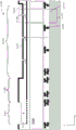
A cross-sectional view of the integrated device 1-102 illustrating a row of pixels 1-112 is shown in fig. 1-1. The integrated devices 1-102 may include coupling regions 1-201, routing regions 1-202, and pixel regions 1-203. As discussed herein, the optical system of the integrated device may include different types of optical components that may be located within regions 1-201, 1-202, and 1-203 of the integrated device. Coupling regions 1-201 may include grating couplers 1-216, which may be configured to receive excitation light (shown by dashed arrows) and propagate the excitation light to one or more optical components in routing regions 1-202. Routing areas 1-202 may include an optical routing network configured to separate light among a plurality of waveguides 1-220 and to propagate the light to pixel areas 1-203. Pixel regions 1-203 may contain a plurality of pixels 1-112 having sample wells 1-108 positioned on the surface at locations separate from the coupling regions 1-201 where excitation light (shown by dashed arrows) is coupled to the integrated device 1-102. Sample wells 1-108 may be formed through metal layers 1-106. One pixel 1-112, illustrated by a dashed rectangle, is the region of the integrated device 1-102 that contains the sample well 1-108 and the photodetector region with one or more photodetectors 1-110.
1-1 illustrate an excitation light path (shown in dashed lines) through an integrated device by coupling an excitation light beam to coupling regions 1-201 and directing the excitation light to sample wells 1-108. The rows of sample wells 1-108 shown in fig. 1-1 may be positioned to optically couple with the waveguides 1-220. The excitation light may illuminate a sample located within the sample well. The sample may reach an excited state in response to being illuminated by the excitation light. When the sample is in the excited state, the sample may emit emission light that is detectable by one or more light detectors associated with the sample well. Fig. 1-1 schematically illustrates an emission light path (shown as a solid line) from a sample well 1-108 of a pixel 1-112 to a light detector 1-110. Photodetectors 1-110 of pixels 1-112 may be configured and positioned to detect emitted light from sample wells 1-108. Examples OF suitable photodetectors are described in U.S. patent application 14/821,656 entitled "INTEGRATED DEVICE FOR TEMPORAL BINNING OF RECEIVED PHOTONS," which is incorporated herein by reference in its entirety. Additional examples of suitable photodetectors are described in U.S. patent application No. 15/852,571 entitled "INTEGRATED PHOTODETECTOR WITH DIRECT BINNING PIXEL" filed on 22.12.2017, which is incorporated herein by reference in its entirety. The sample wells 1-108 and their respective photodetectors 1-110 may be aligned along a common axis (along the y-direction shown in fig. 1-1) for the individual pixels 1-112. In this manner, the light detector may overlap the sample well within pixels 1-112.
A plan view of an integrated device 1-102 illustrating five rows of pixels is shown in fig. 1-2. As shown in fig. 1-2, sample wells 1-108a are in the same row as sample wells 1-108b and sample wells 1-108c are in the same row as sample wells 1-108 d. Aspects of the present application are directed to techniques for receiving excitation light incident to coupling regions 1-201 and propagating the excitation light to an array of sample wells 1-108. The techniques may include positioning one or more optical grating couplers in the coupling regions 1-201 and waveguide architecture, in the routing regions 1-202 and/or pixel regions 1-203 for communicating excitation light from the coupling regions 1-201 to the individual sample wells 1-108.
B.Waveguide architecture
Some embodiments pertain to integrated devices having one or more tapered waveguides. The tapered waveguide has one or more dimensions that vary along the length of the waveguide and in the direction of light propagation through the waveguide. For example, a waveguide having a varying width along its length may be considered a tapered waveguide. The characteristics of the light propagating along the tapered waveguide may vary depending on the changing dimension or dimensions of the tapered waveguide. In the context of distributing light in a substantially uniform manner among an array of sample wells, a tapered waveguide may be implemented as a technique that provides a similar amount of light intensity among a group of sample wells located proximate to the tapered waveguide. In some embodiments of the integrated device, the tapered waveguide may be positioned to couple with a row of sample wells in the array of sample wells, with the taper of the waveguide being appropriately sized to allow for a similar amount of light intensity at individual sample wells in the row. A tapered waveguide may be evanescently coupled with the sample wells in the row and the width of the waveguide may be tapered to provide a weaker evanescent field at the light input end closer to the waveguide and a stronger evanescent field at the light input end further from the waveguide. This waveguide configuration may allow for a more uniform excitation intensity to be delivered by the waveguide in the row of the sample well than if a waveguide with a constant width were used.
Fig. 2-1A illustrates a plan view of sample wells in a row along a tapered waveguide 2-220, including sample wells 1-108e and 1-108f, where light is input to the waveguide 2-220 at the side corresponding to the arrow shown in fig. 2-1A and propagates along the z-direction. As shown in fig. 2-1A, the width of the tapered waveguides 2-220 varies along the row of sample wells, with the waveguides 2-220 having a larger width near the input side (closer to the arrows) than far from the input side. Thus, sample wells 1-108e are positioned over a region of waveguides 2-220 that has a width greater than the region of waveguides 2-220 over which sample wells 1-108f are positioned. Fig. 2-1B is a cross-sectional view of the row of sample wells 1-108 shown in fig. 2-1A and illustrates how the optical mode profile varies along the length (along the z-direction) of the tapered waveguides 2-220. As light propagates along the tapered waveguides 2-220, the changing optical mode profile affects the amount of intensity reaching the illuminated area near the bottom of the sample well. In particular, the larger widths of the tapered waveguides 2-220 proximate to the sample wells 1-108e provide less intensity within the illuminated areas of the sample wells 1-108e, while the smaller widths of the tapered waveguides 2-220 proximate to the sample wells 1-108f have greater intensity within the illuminated areas of the sample wells 1-108 f. In some embodiments, one or more characteristics (e.g., thickness, material) of the top cladding layer 2-222 may affect the tapered shape of the waveguide 2-220.
In addition, the tapered waveguide may have a configuration that accounts for optical losses along the length of the waveguide, including optical losses associated with absorption and scattering by sample wells positioned proximate to the waveguide. In some embodiments, the configuration of the taper of the waveguide may provide a desired power efficiency across the array of sample wells such that variations in the intensity of light received by the sample wells caused by optical power loss are reduced or prevented as the light propagates along the waveguide. This configuration may allow optical power loss to be effectively eliminated as a factor leading to non-uniform excitation light transmission across the array of sample wells.
In particular, the power in the waveguide is as a function And a reduction in propagation loss alpha as a function of waveguide width, top cladding configuration (e.g., top cladding thickness, material), and sample well configuration (e.g., sample well depth). In addition, the intensity within the illuminated region of the sample well depends on the waveguide width, the top cladding configuration (e.g., top cladding thickness, material), and the sample well configuration (e.g., sample well depth). In determining the tapered shape of the tapered waveguide, the size of the waveguide at a particular location may depend on the power loss associated with the previous sample well and the width of the waveguide required to achieve the desired intensity at that location. In some embodiments, the tapered waveguides 2-220 may have a non-linear tapered shape. In this embodiment, the waveguide width may be bounded by a maximum and a minimum and the variation along the width of the waveguide may vary non-linearly to achieve substantially uniform intensity among all sample wells coupled to the waveguide. In some embodiments, the tapered waveguides 2-220 may have a linear shape, with the width of the waveguide varying linearly between a maximum and a minimum to achieve substantially uniform intensity among all sample wells coupled to the waveguide.
According to some embodiments set forth herein, a "substantially uniform intensity" may be determined for a particular waveguide by correlating a highest intensity received by a sample well positioned to couple with the waveguide with a lowest intensity received by a sample well positioned to couple with the waveguide. In some embodiments, a "substantially uniform intensity" for a group of sample wells coupled to a waveguide may correspond to a ratio of highest intensity to lowest intensity received by the sample wells in the group being approximately equal to 1 (e.g., equal to 1 ± 5%, equal to 1 ± 10%).
The thickness of the top cladding layers 2-222 may affect the uniformity of the intensity received by the sample wells in the row. Fig. 2-2 and 2-3 show simulation results in which a waveguide with a top cladding thickness variation and a non-linear taper is designed to achieve a relative intensity minimum for a row of 1024 sample wells. The waveguide has a thickness of 120nm, a minimum width value of 300nm and a maximum width value of 1300 nm. The sample well has a depth of 300 nm. Fig. 2-2 shows the power input to the waveguide versus top cladding thickness required to reach the minimum relative intensity across all 1024 sample wells. The relationship shown in fig. 2-2 illustrates how there is an optimum value for the thickness of the top cladding layer 2-222 between 380nm and 400nm, where the input power to the waveguide is at a minimum. 2-3 show graphs of the amount of intensity non-uniformity along a row of sample wells versus the thickness of the top cladding, where the non-uniformity corresponds to the ratio of the highest intensity at the sample well to the lowest intensity at the sample well. A non-uniformity value equal to 1 corresponds to the highest intensity being equal to the lowest intensity value and thus corresponds to a scenario in which there is a uniform intensity at all sample wells in the row. Turning to both fig. 2-2 and 2-3, there is a balance between input power, top cladding thickness, and non-uniformity. In particular, when the top cladding layer is thicker than its optimum, a non-uniformity equal to 1 may be achieved but at a higher input power than if the top cladding thickness were at its optimum.
Fig. 2-4, 2-5, and 2-6 show simulation results for tapered waveguides configured for a row of 1024 sample wells having a 395nm top cladding thickness layer. 2-4 are graphs of relative intensity versus number of sample wells and show how the relative intensity at individual sample wells is uniform across all sample wells. Fig. 2-5 are graphs of power in the waveguide versus the number of sample wells in the row and show how the optical power decreases along the row of sample wells. Fig. 2-6 are graphs of waveguide width versus number of sample wells in a row and illustrate the tapered profile of the waveguide for obtaining the uniform intensity shown in fig. 2-4.
The length of the waveguide and the number of sample wells in the row are additional parameters that may affect the uniformity of intensity distributed among the rows of sample wells. Fig. 2-7 and 2-8 show simulation results for tapered waveguides designed to have uniform intensity for different numbers of sample wells in a row. Specifically, fig. 2-7 are graphs of power input to the waveguide versus the number of sample wells per row and fig. 2-8 are graphs of row efficiency (which corresponds to the number of sensors per unit power) versus the number of sample wells per row. As shown in fig. 2-7, the input power increases as the number of sample wells in the row increases. Fig. 2-8 illustrate how efficiency decreases as the number of sample wells in the row increases.
While the use of tapered waveguides in integrated devices may provide certain benefits in conveying excitation light in a substantially uniform manner among sample wells, there may be limitations in using tapered waveguides as integrated devices scale by increasing the number of sample wells. As discussed in connection with fig. 2-7 and 2-8, as the number of sample wells in a row increases, more power input to the waveguide is required and the row efficiency decreases. The inventors have recognized and appreciated that using multiple waveguides to couple with a row of sample wells may overcome this limitation associated with using only tapered waveguides. The use of multiple waveguides may allow longer rows of sample wells to have substantially uniform intensity than would otherwise be achieved using a single tapered waveguide. Accordingly, some embodiments pertain to an integrated device having a plurality of waveguides configured to optically couple with a row of sample wells. According to some embodiments, this configuration may be used in combination with a tapered waveguide. In this embodiment, the plurality of waveguides optically coupled to a single row of sample wells may be tapered at least in the region where the waveguides are coupled to a subset of the sample wells in that row. This configuration may allow rows with a higher number of sample wells to receive similar intensities than using a single waveguide.
In some embodiments of the integrated device, the first waveguide is positioned to optically couple with a first set of sample wells in the row and the second waveguide is positioned to optically couple with a second set of sample wells in the row. Between the first and second sets of samples, the first and second waveguides may be displaced in position relative to the rows of sample wells. This configuration can be considered as having a waveguide "row shift" between the first and second sets of sample wells. The position of the row shift may correspond to when the coupling efficiency of the first waveguide to the row of sample wells or the power propagating within the first waveguide drops to a certain amount such that the performance of the device is affected. Using the second waveguide to continue transmitting light to subsequent sample wells in the row eliminates this limitation of using only the first waveguide. Additional waveguides may be included and positioned to optically couple with additional sets of sample wells in the same row. This waveguide configuration may be implemented in other rows in the array of sample wells to increase the number of sample wells in the array (such as by increasing the number of sample wells in a separate row).
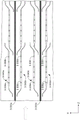
Fig. 3-1 is a plan view of an integrated device illustrating a row-shifting waveguide configuration in which multiple waveguides are used to deliver light to individual rows of sample wells. The direction of light input to the waveguide is shown by the arrow and is in the z-direction. FIG. 3-1 shows three rows of sample wells, including rows with sample wells 3-108a, 3-108b, and 3-108c, and rows with sample wells 3-108d, 3-108e, and 3-108f, with three waveguides positioned to optically couple (e.g., evanescently couple) with three different sets of sample wells in the row. For example, the waveguides 3-220a are positioned to optically couple with the sample wells 3-108a, while the waveguides 3-220b are positioned to optically couple with the sample wells 3-108 c. As another example, the waveguides 3-220d are positioned to optically couple with the sample wells 3-108d, while the waveguides 3-220e are positioned to optically couple with the sample wells 3-108 f. Optical coupling of the waveguide can occur through evanescent coupling, where the waveguide is positioned at a suitable distance below the sample well (such as shown by waveguides 1-220 in fig. 1-1) so that the sample well receives a portion of an optical mode propagating along the waveguide. According to some embodiments, waveguides 3-220a may be positioned to evanescently couple with other sample wells in the same row within sample wells 3-108a and regions 3-110, and waveguides 3-220b may be positioned to evanescently couple with other sample wells in the same row within sample wells 3-108c and regions 3-114. Additional waveguides may be used to convey light to subsequent sample wells in the same row. For example, FIG. 3-1 shows waveguides 3-220c and 3-220f that may be coupled with additional sample wells that are not present in the view shown in FIG. 3-1. In particular, after an additional row of shifted regions behind regions 3-114, waveguides 3-220c may be coupled with sample wells in the same row as sample wells 3-108c and waveguides 3-220e may be coupled with sample wells in the same row as sample wells 3-108 f.
Sample wells in the same row may correspond to sample wells that are substantially aligned along a common axis. The sample well groups in zones 3-110 may be substantially aligned along an axis for a particular row. As shown in fig. 3-1, sample wells 3-108a, 3-108b, and 3-108c are aligned along an axis (in the z-direction) and are considered to be in the same row. The waveguide may be positioned relative to the axis. In some embodiments, a portion of the waveguides configured to couple with a set of sample wells may be substantially parallel to the axis, and a plurality of waveguides may be optically coupled with different sets of sample wells and substantially parallel to the axis at different portions along a row of sample wells. As shown in fig. 3-1, waveguides 3-220a are substantially parallel to an axis along sample wells 3-108a, 3-108b, and 3-108c in region 3-110 and waveguides 3-220b are substantially parallel to the axis in region 3-114.
The spacing between the waveguides may be such that the waveguides are effectively optically decoupled from each other. In some embodiments, one waveguide may be separated from another waveguide such that there is no or very little evanescent coupling between the two waveguides. In some embodiments, the lateral distance between two waveguides may depend on the size of the optical mode that the waveguides are configured to have.
The waveguide configuration shown in fig. 3-1 has regions 3-110, 3-112, and 3-114. Regions 3-110 are where a first waveguide (such as waveguide 3-220a) is optically coupled to a first set of sample wells in the row (such as sample wells 3-108a) so as to transmit light to the first set of sample wells. Regions 3-114 are where a second waveguide (such as waveguide 3-220b) is optically coupled to a second set of sample wells in the row (such as sample wells 3-108c), thereby transmitting light to the second set of sample wells. Regions 3-112 correspond to where the line shift between the first waveguide and the second waveguide occurs. As shown in fig. 3-1, the row shifting configuration includes bending the waveguides such that the first waveguide is not positioned to optically couple with the sample wells in the row, while the second waveguide is positioned to optically couple with the sample wells in the row. The row-shifting configuration results in the distance between the first waveguide and the sample well in regions 3-110 being less than the distance between the first waveguide and the sample well in regions 3-112. The row-shifting configuration further results in the distance between the second waveguide and the sample well in regions 3-114 being less than the distance between the second waveguide and the sample well in regions 3-112. For example, waveguides 3-220a and 3-220d are curved in regions 3-112 to be offset (along the x-direction) from their respective sample well rows, with the offset increasing along the direction of light propagation through the waveguides. In addition, waveguides 3-220b and 3-220e are bent in regions 3-112 and offset from their respective rows of sample wells (along the x-direction), but the offset decreases along the direction of light propagation through the waveguides to position waveguides 3-220b and 3-220e closer to the rows of sample wells. The row shift profiles in regions 3-112 may have any suitable profile and/or length. While the waveguides shown in fig. 3-1 have similar row-shifting profiles in regions 3-112, it should be appreciated that some embodiments may involve coupling to waveguides in the same row having different profiles within regions 3-112.
In some embodiments, the region of the waveguide configured to optically couple with the sample wells in a row may be tapered (such as by using the techniques set forth herein) to achieve substantially uniform intensity for the set of sample wells to which the waveguide is coupled in that region. As shown in fig. 3-1, waveguides 3-220a are tapered in region 3-110 and waveguides 3-220b are tapered in region 3-114.
The integrated device may contain one or more optical components (e.g., optical splitters shown in fig. 1-1 located within routing regions 1-202) to provide input power into individual waveguides. In some embodiments, the input power may be substantially the same across all waveguides. The inventors have recognized and appreciated that a waveguide that is not optically coupled to a set of sample wells in a row may experience some optical loss as light propagates through this region. Accordingly, some embodiments may have configurations that reduce this optical loss by varying one or more characteristics of the waveguide in the region where the waveguide is optically coupled to the respective sample well. For example, the portion of waveguides 3-220b in regions 3-110 may have a configuration to reduce optical losses, but may still deliver a lower amount of power when waveguides 3-220b are optically coupled to sample wells in regions 3-114 than when waveguides 3-220a are optically coupled to sample wells in regions 3-110. Thus, the taper of the waveguide that conveys light to the row of sample wells may be different to account for this variation in optical power when the waveguide is used to couple to the sample wells. In some embodiments, the length of the tapered portion of the first waveguide in regions 3-110 may be different than the length of the tapered portion of the second waveguide in regions 3-114. The length of the tapered portion may correspond to the number of sample wells that a particular waveguide is used to deliver light to within that tapered region of the waveguide. In some embodiments, the tapered portion of the second waveguide in regions 3-114 may have a shorter length than the tapered portion of the first waveguide in regions 3-110. This configuration may account for the second waveguide having a lower optical power in regions 3-114 than the first waveguide has in regions 3-110. For example, FIG. 3-1 shows that the tapered portion of waveguide 3-220a in region 3-110 is coupled with six sample wells, which may correspond to the length of the tapered portion of waveguide 3-220a, while the tapered portion of waveguide 3-220b in region 3-114 is shown coupled with five sample wells. It should be appreciated that the tapered portions of the first and second waveguides may be coupled with more or fewer sample wells than shown in fig. 3-1.
In some embodiments, sample wells located within a row of waveguides where row shifting occurs may not be optically coupled to a waveguide or have a lower amount of optical coupling to a waveguide than other sample wells in the row. Thus, sample wells located within the row shift region of the array of sample wells may receive a lower amount of optical power. During operation of the integrated device when performing an analysis of a sample, the sample well may be excluded from the results of the analysis, since the quality of the results obtained through the sample well may be affected by an insufficient ability to irradiate the sample with a desired amount of light (e.g., a particular intensity). As shown in fig. 3-1, the group of sample wells in regions 3-112 may receive less optical power than the same row of sample wells in regions 3-110 or sample wells in regions 3-114. This is because the sample wells positioned in regions 3-112 may not be optically coupled or not at a desired efficiency with the corresponding first or second waveguides of the row. For example, regions 3-112 include sample wells 3-108b, and sample wells 3-108b may receive lower amounts of optical power than sample wells in regions 3-110 and 3-114 (such as sample wells 3-108a and 3-108c), because sample wells 3-108b are offset from both waveguides 3-220a and 3-220 b. Similarly, regions 3-112 include sample wells 3-108e, and sample wells 3-108e may receive a lower amount of optical power than sample wells 3-108d and 3-108 f. Thus, data obtained from using sample wells 3-108b and 3-108e during operation of the integrated device may be excluded from the overall results.
Waveguide arrays having row-shifting configurations, such as that shown in fig. 3-1, can be implemented in an integrated device in combination with one or more of the other components set forth herein. In some embodiments, an integrated device having a row-shifted waveguide configuration may include a grating coupler configured to receive light from a surface of the integrated device and optically couple with a waveguide. In the context of fig. 3-1, the grating coupler may be positioned to the left (in the negative z-direction) to provide light in the direction of the arrow shown in fig. 3-1. In some embodiments, an integrated device having a row-shifting waveguide configuration may include one or more light detectors configured to receive light emitted from a sample well located in the same pixel as the one or more light detectors. For example, a pixel having a sample well 3-108a may include one or more photodetectors positioned and configured to receive light emitted from the sample well 3-108 a. The pixel may have a cross-sectional configuration as illustrated by pixels 1-112 in fig. 1-1.
The inventors have recognized and appreciated that an arrayed waveguide configuration having a waveguide per row of sample wells, which acts as an optical power source and is optically coupled to one or more other waveguides positioned to optically couple with the sample wells in the row, may provide particular benefits. A waveguide that acts as an optical power source may be considered a "power waveguide". One benefit of this configuration is that the overall footprint of the arrayed waveguides can be reduced, which can provide advantages in configuring integrated devices where the distance between rows of sample wells is small and may not accommodate multiple waveguides positioned between rows of sample wells. Accordingly, some embodiments of an integrated device may include power waveguides associated with individual rows of an array of sample wells and one or more waveguides optically coupled with one or more power waveguides and sample wells in a corresponding row. In some embodiments, one or more other waveguides may be optically coupled to the power waveguide through an optical splitter (e.g., a directional coupler). In some embodiments, a row of sample wells has a waveguide that acts as a continuous coupler that is optically coupled with the power waveguide associated with the row and with the sample wells in the row.
Fig. 3-2 is a plan view of an integrated device having an arrayed waveguide configuration that includes, for a row of sample wells, a power waveguide and a plurality of waveguides positioned to optically couple with different sets of sample wells in the row. Sample wells 3-208a and 3-208b are in the same row, and waveguide 3-230a acts as a power waveguide for that row. Similarly, sample wells 3-208c and 3-208d are in different rows, and waveguides 3-230b act as power waveguides for that row. The direction of light propagation along the power waveguide is shown by the arrows in fig. 3-2. Along the power waveguide, a separate waveguide is coupled with the power waveguide and positioned to optically couple with a set of sample wells in the row. In fig. 3-2, waveguides 3-240a and 3-240b are configured to optically couple with power waveguides 3-230a and deliver light to sample wells in rows having sample wells 3-208a and 3-208 b. In some embodiments, waveguides 3-240a and 3-240b are tapered to provide substantially uniform intensity for a sample well optically coupled to the waveguide (such as by using the tapered waveguides set forth herein). As shown in fig. 3-2, the sample well 3-208a is configured to optically couple with a region of the waveguide 3-240a having a width greater than a region of the waveguide 3-240a to which the sample well 3-208b is optically coupled. Similarly, sample well 3-208f is configured to optically couple with a region of waveguide 3-240b that has a width greater than the region of waveguide 3-240b to which sample well 3-208g is optically coupled. In addition, sample wells 3-208c and 3-208d in a different row than sample wells 3-208a and 3-208b are configured to optically couple with different regions of the waveguide 3-240c having different widths. In particular, sample wells 3-208c are configured to optically couple with a region of waveguide 3-240c having a width greater than a region of waveguide 3-240c to which sample wells 3-208d are optically coupled.
The power waveguides 3-230a and 3-230b may have configurations that reduce optical losses as light propagates along the waveguides (such as by having a substantially uniform width along the length of the waveguides). As shown in fig. 3-2, waveguides 3-240a and 3-240b may be optically coupled to power waveguides 3-230a via power splitters 3-250a and 3-250b, respectively. In addition, waveguides 3-240c and 3-240d may be optically coupled to power waveguides 3-230b via one or more power splitters. Examples of suitable power splitters include directional couplers, multimode interference splitters, or any other suitable power-splitting optical component. In embodiments in which a directional coupler is used as the power splitter, the configuration of the directional coupler may be configured for a particular power splitting ratio to achieve a desired relative amount of optical power that is input into a set of optically coupled waveguides with the sample well.
In some embodiments, separate power splitters optically coupled to the power waveguide may have similar splitting ratios. Referring to fig. 3-2, the power splitters 3-250a and 3-250b may have the same splitting ratio as the power waveguides 3-230 a. In this case, waveguide 3-240b is configured to receive less optical power than waveguide 3-240a as light propagates along 3-230a, since power waveguide 3-230a is coupled with power splitter 3-250a before power splitter 3-250 b. In this embodiment, the waveguides 3-240a and 3-240b may have different taper shapes to accommodate differences in input power, such that the sample well is configured to optically couple with the waveguides 3-240a and 3-240b that receive substantially similar intensities, and thus the different taper shapes of the waveguides 3-240a and 3-240b may account for differences in optical power received by the waveguides 3-240a and 3-240b from the power waveguides 3-230a via the power waveguides 3-250a and 3-250 b. For example, the waveguides 3-240b may have a shorter taper length than the waveguides 3-240a to account for the lower input power received from the power waveguides 3-230 a.
In some embodiments, the individual power splitters optically coupled to the power waveguide may have different splitting ratios such that the waveguide optically coupled to the sample well receives substantially similar input power. Referring to fig. 3-2, the power splitters 3-250a and 3-250b may have different splitting ratios than the power waveguides 3-230a so that similar amounts of optical power are coupled to the waveguides 3-240a and 3-240 b. In this embodiment, the waveguides 3-230a and 3-230b may have a similar tapered shape to allow the sample wells optically coupled with the waveguides 3-230a and 3-230b to receive substantially similar intensities.
Some embodiments may include transition regions between individual waveguides optically coupled to sample wells within a row. Sample wells located within the transition region may not be positioned to optically couple with one of the waveguides or receive similar amounts of optical power as other sample wells in the row outside of the transition region. As shown in fig. 3-2, sample well 3-208e is an example of a sample well located in the transition region between waveguides 3-240a and 3-240 b. Sample wells 3-208e may receive a lower amount of optical power than sample wells 3-208a and 3-208 b. In this case, any data obtained using sample wells 3-208e may be excluded from analysis because the sample wells receive a lower amount of excitation light than other sample wells, such as sample wells 3-208a and 3-208 b.
In some embodiments, the integrated device may include more than one upstream power waveguide configured to deliver optical power to the sample well. Fig. 3-3 is a plan view of an integrated device having a power waveguide 3-330a configured to deliver light to two rows of sample wells adjacent to the power waveguide 3-330 a. In particular, power waveguides 3-330a are configured to optically couple with rows of sample wells including sample wells 3-308a and 3-308b and rows of sample wells including sample wells 3-308c and 3-308 d. As in the configuration shown in fig. 3-3, the sample wells in these two rows may be optically coupled to the power waveguides 3-330a through the combination of the waveguides and the power splitter. The waveguides 3-340a are positioned to optically couple with the sample wells 3-308a and 3-308b and may be optically coupled to the power waveguides 3-330a via a power splitter. Waveguides 3-340b are positioned to optically couple with sample wells 3-308c and 3-308d and may be optically coupled to power waveguides 3-330a via power splitters. The waveguides and power splitters described in connection with fig. 3-3 may be used for waveguides 3-340a and 3-340b and power splitters are used to couple the waveguides to power waveguides 3-330 a. Similarly, power waveguides 3-330b are configured to deliver light to rows of sample wells including sample wells 3-308e and 3-308f, and to rows of sample wells including 3-308g and 3-308 h. In particular, waveguides 3-340c are positioned to optically couple with power waveguides 3-330b and sample wells 3-308e and 3-308f, and waveguides 3-340d are positioned to optically couple with power waveguides 3-330b and sample wells 3-308g and 3-308 h.
In some embodiments, a waveguide positioned to optically couple with a sample well in a row may be connected to a power waveguide (such as through one end of the power waveguide). For example, in a waveguide configuration in which there is a series of waveguides configured to optically couple with a row of sample wells and light is optically coupled to the series of waveguides through a power waveguide, the waveguides in the series distal to the light input end of the power waveguide may be directly connected to the power waveguide (such as through an optical connection). In this configuration, light propagating along the power waveguide may be delivered to the waveguide by propagating through the optical connection. Fig. 3-4 are plan views of waveguide configurations with power waveguides 3-430, where the arrows show the light input direction to the power waveguides 3-430. Waveguides 3-440a, 3-440b, 3-440c, and 3-440d are configured to optically couple with rows of sample wells having sample wells 3-408a, 3-408b, 3-408c, and 3-408 d. Waveguides 3-440a, 3-440b, and 3-440c are optically coupled to power waveguides 3-430 through power splitters 3-450a, 3-450b, and 3-450c, respectively. The waveguides 3-440d are connected to the power waveguide through optical connections 3-460. The optical connections 3-460 may be of any suitable size and shape to direct light output from the power waveguides 3-430 to the waveguides 3-440 d.
Some embodiments may include a power waveguide having a varying width along its length. As shown in fig. 3-4, the power waveguide 3-430 has a narrowed width in a region where the power waveguide 3-430 is optically coupled with the power splitters 3-450a, 3-450b, and 3-450 c. The width of the power waveguide 3-430 is larger in the region between the power dividers 3-450a, 3-450b, and 3-450c than in the region overlapping with the power dividers 3-450a, 3-450b, and 3-450 c.
It should be appreciated that the power waveguides, power splitters, and waveguides optically coupled to the sample wells within a particular row may be suitably configured to accommodate optical losses experienced by light propagating through the waveguide configuration. By way of example, in the waveguide configuration shown in fig. 3-4, power splitters 3-450a, 3-450b, and 3-450c may be configured to have power splitting ratios of 22%, 30%, and 48%, respectively. If the power waveguide 3-430 has about a 10% power loss between the individual waveguides 3-440a, 3-440b, 3-440c and 3-440d, the relative input power to the power waveguide 3-430 required to illuminate all sample wells in the row is 4.70. If waveguides 3-440a, 3-440b, 3-440c, and 3-440d are each used to deliver light to 512 sample wells, the input power is about 7.5a.u. arbitrary units). In this example, the row efficiency corresponding to the number of sample wells per unit power is about 273. This configuration for illuminating a total of 2048 sample wells (512 sample wells for each of the four waveguides) is in contrast to using a single tapered waveguide for illuminating all 2048 samples. In a single tapered waveguide configuration, the input power into the tapered waveguide is about 16.8a.u. and the row efficiency is about 122. This example illustrates how the configuration shown in fig. 3-4 can provide increased coupling efficiency within an array of sample wells while reducing the necessary input power.
Some embodiments pertain to a waveguide configuration having a power waveguide configured to optically couple with another waveguide along a length of the power waveguide, wherein the other waveguide is configured to optically couple with a sample well within a row. In some embodiments, the other waveguide and the power waveguide are configured to evanescently couple to each other. Another waveguide may be positioned relative to the power waveguide to achieve a desired coupling strength such that the waveguide that delivers light to the row of sample wells has substantially uniform power along the length of the waveguide. In this way, the power waveguide is configured to compensate for optical losses experienced by another waveguide configured to provide similar intensities to the sample well to which it is optically coupled. Since another waveguide is optically coupled to the power waveguide along its length, the waveguide can be considered a "continuous coupler" waveguide. According to some embodiments, the continuous coupler waveguide may be configured to weakly couple with the power waveguide over a length in the range of 1mm to 10mm, or any value or range of values in that range.
Fig. 3-5 are plan views of integrated devices having a waveguide configuration that includes a power waveguide and a continuous coupler waveguide for individual sample well rows. The power waveguide 3-530 is configured to optically couple with a waveguide 3-540 that is optically coupled with a sample well in a row with sample wells 3-508. The arrows show the light input direction to the power waveguides 3-530. The waveguide 3-540 is configured to optically couple with the power waveguide 3-530 along the length of the waveguide 3-540. In some embodiments, the power waveguide 3-530 and the waveguide 3-540 are evanescently coupled to each other along the length of the waveguide 3-540. In particular, the coupling strength between the power waveguide 3-530 and the waveguide 3-540 is configured to compensate for the optical loss experienced by the waveguide 3-540 as light propagates along the waveguide 3-540 and couples into the sample well in the row. For example, the waveguide has higher propagation losses than the power waveguide 3-530 due to losses caused by the sample well acting as a light scattering along the waveguide 3-540. In some embodiments, the power waveguide 3-530 may be configured to have a higher amount of power proximate to the input end of the power waveguide 3-530 than the waveguide 3-540 has proximate to its input end.
In some embodiments, the power waveguide may be coupled with a "continuous coupler" waveguide through a power splitter (e.g., directional coupler, multimode interference splitter). As shown in fig. 3-5, the power splitter 3-550 is configured to direct a portion of the light propagating through the power waveguide 3-530 into the waveguide 3-540. The amount of power provided by the power splitter 3-550 to the waveguide 3-540 can be considered the initial amount of power and the coupling strength between the power waveguide 3-530 and the waveguide 3-540 is configured to compensate for the power loss in the waveguide 3-540. In some embodiments, the power divider 3-550 may be configured to have a division ratio in the range between 5% and 50%, or any value or range of values in that range. The power splitter 3-550 may provide a high degree of coupling between the power waveguide 3-530 and the waveguide 3-540 over a distance in the range of 5 μm to 50 μm, or any value or range of values in that range. The distance within which the power splitter 3-550 provides coupling between the power waveguide 3-530 and the waveguide 3-540 may be considered the "coupling length" of the power splitter 3-550. In some embodiments, the coupling length of the power divider (e.g., directional coupler) may be less than about 100 μm.
The strength of the optical coupling between the power waveguide 3-530 and the waveguide 3-540 may depend on the characteristics of the two waveguides, including the dimension D of the gap between the power waveguide 3-530 and the waveguide 3-540, the width of the power waveguide 3-530, the width of the waveguide 3-540, and the refractive indices of the power waveguide 3-530 and the waveguide 3-540. For example, decreasing the dimension D of the gap between the power waveguide 3-530 and the waveguide 3-540 increases the strength of the optical coupling between the power waveguide 3-530 and the waveguide 3-540. In some embodiments, the coupling strength between the power waveguide 3-530 and the waveguide 3-540 may be substantially constant along the length of the waveguide 3-540. In this embodiment, the dimension D of the gap may be substantially constant along the length of the waveguide 3-540, as shown in FIGS. 3-5.
In some embodiments, the coupling strength between the power waveguide and the continuous coupler waveguide may vary along the length of the continuous coupler waveguide, which may allow the power waveguide to compensate for propagation losses along the continuous coupler waveguide. In this embodiment, the dimension D of the gap between the two waveguides may vary along the length of the continuous coupler waveguide. Fig. 3-6 are plan views of waveguide configurations having a power waveguide 3-530 optically coupled to a waveguide 3-540, wherein the size of the gap between the power waveguide and the waveguide varies along the length of the waveguide 3-540. In particular, the power waveguide 3-530 is angled toward the waveguide 3-540 such that at locations proximate to the power input (shown by the arrow), the distance D1 between the power waveguide 3-530 and the waveguide 3-540 is greater than the distance D2 at locations distal from the power input. In this configuration, the coupling strength between the power waveguide 3-530 and the waveguide 3-540 increases along the length of the waveguide 3-540.
One parameter that can affect the length of a continuous coupler waveguide, or the number of sample wells to which the waveguide can be optically coupled, is the coherence length, or the distance within which light propagates along the power waveguide and the continuous coupler waveguide is in phase. If the coherence length is short, the number of sample wells to which the continuous coupler waveguide can deliver light becomes small. The inventors have recognized and appreciated that having different widths for the power waveguide and the continuous coupler waveguide can offset the phase difference between the two waveguides and thus increase the coherence length. Thus, some embodiments involve different widths for the power waveguides 3-530 and waveguides 3-540. In some embodiments, the power waveguide 3-530 has a width dp that is less than the width dc of the waveguide 3-540. In some embodiments, the power waveguide 3-530 has a width dp that is greater than the width dc of the waveguide 3-540.
3-5 and 3-6 show the power waveguides 3-530 and the waveguides 3-540 located within the same layer of the integrated device and configured to couple laterally to each other, it should be appreciated that the power waveguides 3-530 and the waveguides 3-540 may be configured to couple vertically to each other. In some embodiments, the power waveguides 3-530 and waveguides 3-540 are positioned within different layers of the integrated device. In some embodiments, the power waveguides 3-530 and waveguides 3-540 are positioned to vertically overlap each other. In some embodiments, the waveguide 3-540 may be positioned between the row of sample wells to which it is coupled and the power waveguide 3-530. In this embodiment, the waveguides 3-540 are non-overlapping with the row of sample wells (containing sample wells 3-508) to which they are optically coupled.
In some embodiments, the end of the continuous coupler waveguide distal from the optical input may be tapered. This embodiment may allow increasing the number of sample wells in the row and/or the coupling efficiency with the sample wells that are optically coupled with this region of the waveguide.
Parameters that may affect the extent to which sample wells in a row receive substantially uniform intensity from a continuous coupler waveguide, such as shown in fig. 3-5 and 3-6, may include the thickness of the top cladding layer 2-222, the initial coupling fraction with the power waveguide, the thickness of the continuous coupler waveguide, and the depth of the sample well. Fig. 3-7 and 3-8 show simulation results where the initial coupling fraction to the power waveguide is varied and a continuous coupler waveguide is designed to reach a relative intensity minimum for a row of 1024 sample wells. The waveguide has a thickness of 120nm and a top cladding layer thickness of 325 nm. The sample well has a depth of 300 nm. Fig. 3-7 are graphs of initial coupling fractions of power input to the continuous coupler waveguide versus power waveguide required to reach a minimum relative intensity across all 1024 sample wells. The graphs shown in fig. 3-7 illustrate how there is a minimum power input required when the initial coupling fraction to the power waveguide is about 0.26. Fig. 3-8 are graphs of the amount of intensity non-uniformity along a row of sample wells versus the initial coupling fraction to the power waveguide, where the non-uniformity corresponds to the ratio of the highest intensity at the sample well to the lowest intensity at the sample well. A non-uniformity value equal to 1 corresponds to the highest intensity being equal to the lowest intensity value and thus corresponds to a scenario in which there is a uniform intensity at all sample wells in the row. Turning to both fig. 3-7 and 3-8, when the initial coupling fraction with the power waveguide is less than 0.26, uniform intensity can be achieved among all 1024 sample wells (when the non-uniformity is 1).
3-9, 3-10, and 3-11 show simulation results for 1024 sample wells in rows with a top cladding thickness layer of 325nm and an initial coupling fraction equal to 0.26 for power waveguide and continuous coupler waveguide configurations. Fig. 3-9 are graphs of relative intensity versus number of sample wells and show how the relative intensity at individual sample wells is uniform across all sample wells. Fig. 3-10 are graphs of power in the waveguide versus the number of sample wells in the row and show how the optical power in the power waveguide decreases along the row of sample wells while the continuous coupler waveguide remains constant. Fig. 3-11 are graphs of the size of the gap between the power waveguide and the continuous coupler waveguide versus the number of sample wells and show how the power waveguide is closer to the continuous coupler waveguide at a location away from the input end (corresponding to sample well number 1024).
Waveguide configurations including a power waveguide and a continuous coupler waveguide can provide improved optical efficiency along the row of sample wells for less input power than a single tapered waveguide. As an example, if the waveguides 3-540 are configured to optically couple with 2048 sample wells, the row efficiency corresponding to the number of sample wells per unit power is about 258, with an input power of 7.9a.u. In a single tapered waveguide configuration, the input power into the tapered waveguide is about 16.8a.u. and the row efficiency is about 122. This example illustrates how the configurations shown in fig. 3-5 and 3-6 can provide increased coupling efficiency within an array of sample wells while reducing the necessary input power.
Fig. 3-12 and 3-13 further illustrate how this configuration provides improved optical efficiency for less input power than a single tapered waveguide as the number of sample wells in the row increases. In particular, fig. 3-12 and 3-13 show results obtained by simulating tapered waveguide design and continuous coupler waveguide design for different numbers of sample wells in a row. The tapered waveguide has a width decreasing from 1300nm to 300 nm. The continuous coupler waveguide has a width of 800 nm. Each of the data points represents a waveguide design with uniform intensity among all sample wells at minimum power. Fig. 3-12 are graphs of power input to the waveguide versus the number of sample wells per row. 3-13 are graphs of row efficiency as measured by the number of sample wells per unit power versus the number of sample wells per row. As the number of sample wells increases, the power input for the continuous coupler waveguide is lower than for the tapered waveguide and the row efficiency for the continuous coupler waveguide is greater than for the tapered waveguide.
It should be appreciated that the waveguide configurations described above may be combined in the same integrated device. For example, some embodiments of an integrated device may have a first set of sample well rows configured to receive light from a waveguide having a row shifting configuration and a second set of sample well rows configured to receive light from a continuous coupler waveguide.
Certain aspects of the present disclosure are directed to forming an integrated photonic device having an optical system with one or more of the characteristics of the configurations set forth herein. Some embodiments relate to a method of forming an integrated photonic device, including forming a plurality of sample wells configured in a row, forming a first waveguide positioned to optically couple with at least two sample wells in the row, and forming a second waveguide configured to receive light from a region of the integrated photonic device separate from the row of sample wells and optically couple with the first waveguide.
In some embodiments, the first waveguide is configured to optically couple with the power waveguide along a length of the first waveguide. In some embodiments, the first waveguide is configured to evanescently couple with the power waveguide. In some embodiments, the power waveguide has a greater width than the first waveguide. In some embodiments, the power waveguide is configured to optically couple a first portion of the optical power to the first waveguide and a second portion of the optical power to the second waveguide. In some embodiments, the second waveguide is positioned to optically couple with at least two sample wells in the row. In some embodiments, the method further comprises forming a second plurality of sample wells configured in a second row. A second waveguide is positioned to optically couple with at least two sample wells in the second row.
In some embodiments, the power waveguide is configured to optically couple with the first waveguide through a first directional coupler having a first coupling coefficient and to optically couple with the second waveguide through a second directional coupler having a second coupling coefficient, the second coupling coefficient being greater than the first coupling coefficient. In some embodiments, the second waveguide is positioned to optically couple with at least two sample wells in the row. In some embodiments, the first directional coupler is positioned closer to the optical input of the power waveguide than the second directional coupler. In some embodiments, the method further comprises forming a second plurality of sample wells configured in a second row, wherein a second waveguide is positioned to optically couple with at least two sample wells in the second row.
In some embodiments, the power waveguide is configured to be optically coupled to the first waveguide through a directional coupler having a coupling length of less than about 100 μm. In some embodiments, the coupling strength between the power waveguide and the first waveguide increases along the direction of light propagation through the power waveguide. In some embodiments, the first waveguide has a higher propagation loss than the power waveguide. In some embodiments, the method further comprises forming a grating coupler configured to receive light from a surface of the integrated photonic device and optically couple with the power waveguide.
In some embodiments, the method further comprises forming a second waveguide, wherein the first waveguide is configured to optically couple with a first sample well in the row and the second waveguide is configured to optically couple with a second sample well in the row. In some embodiments, the first waveguide has a tapered end. In some embodiments, the first waveguide is configured to evanescently couple with the power waveguide at a location distal from the tapered end. In some embodiments, the method further includes forming at least one light detector positioned to receive light emitted from a respective one of the at least two sample wells.
Some embodiments relate to a method of forming an integrated photonic device, the method involving forming an array of sample wells configured in a plurality of rows, and forming a plurality of waveguides including a first waveguide positioned to optically couple with a first set of sample wells in a row and a second waveguide positioned to optically couple with a second set of sample wells in the row. In some embodiments, the third set of sample wells in the row is positioned between the first set and the second set. In some embodiments, the third set of sample wells is configured to receive less optical power than the first set of sample wells and/or the second set of sample wells. In some embodiments, the first waveguide is located at a first distance from the first set of sample wells and at a second distance from the third set of sample wells, the first distance being less than the second distance. In some embodiments, the second waveguide is located at a third distance from the second set of sample wells and at a fourth distance from the third set of sample wells, the third distance being less than the fourth distance.
In some embodiments, the first waveguide is curved in a region between the first and second sets of sample wells. In some embodiments, the second waveguide is curved in the region. In some embodiments, a first waveguide is positioned to evanescently couple with each sample well in the first set and a second waveguide is positioned to evanescently couple with each sample well in the second set. In some embodiments, the first waveguide is tapered along a portion configured to evanescently couple with the first set of sample wells, and the second waveguide is tapered along a portion configured to evanescently couple with the second set of sample wells. In some embodiments, the method further comprises forming a grating coupler configured to receive light from a surface of the integrated photonic device and optically couple with the plurality of waveguides. In some embodiments, the first waveguide is optically decoupled from the second set of sample wells and the second waveguide is optically decoupled from the first set of sample wells. In some embodiments, the first set of sample wells and the second set of sample wells are substantially aligned along an axis. In some embodiments, at least a portion of the first waveguide is substantially parallel to the axis. In some embodiments, at least a portion of the second waveguide is substantially parallel to the axis. In some embodiments, the method further comprises forming at least one light detector configured to receive light emitted from a respective sample well in the first group.
C. Grating coupler
As discussed in connection with fig. 1-1, the integrated device may include a grating coupler (such as grating coupler 1-216) configured to receive light from an optical source and direct the light to a waveguide configured to optically couple with an array of sample wells. The inventors have recognized and appreciated that certain grating coupler configurations provide one or more benefits to integrated devices, including higher coupling efficiency of light with other optical components in the device and wider tolerance to angles of incident light. A grating coupler comprises a plurality of structures or grating teeth of one material separated by gaps filled with a different material. The material structure may have a higher index of refraction than the gap material (e.g., the material structure is formed of silicon nitride and the gap is formed of silicon oxide). Parameters that may affect the coupling efficiency of a grating coupler include the width of the material structure, the number of material structures, the width of the gap, and a fill factor, which is the ratio of the width of the material structure to the width of the gap.
Some embodiments are directed to an integrated device having an apodized grating coupler configured to receive light incident on the integrated device. The apodized grating coupler may have material structures that are spaced apart from each other with a variable fill factor. In some embodiments, the material structures may be spaced apart from each other by a gap having a variable width. In some embodiments, the material structure may have a variable width.
FIG. 4-1 is a cross-sectional view of an apodized grating coupler 4-100 configured to optically couple with a waveguide 4-220 wherein light is configured to propagate in the direction shown by the arrows. Light incident on the grating coupler 4-100 is shown by the dashed lines. The apodized grating couplers 4-100 may provide improved phase matching with the incident light. The grating coupler 4-100 has material structures, including material structures 4-120a, 4-120b, and 4-120c, that are spaced apart from one another by a variable fill factor (e.g., a percentage of the grating pitch occupied by the material structures). The fill factor for the material structure of the grating coupler 4-100 increases in the direction towards the waveguide 4-220, which is the light propagation direction. The material structure may have a variable width (along the positive z-direction) corresponding to dimension T. As shown in fig. 4-1, the material structure of the grating coupler 4-100 has a width that increases in a direction toward the waveguide 4-220. For example, material structures 4-120c have a greater width than material structures 4-120 a. The material structures are separated by gaps, including gaps 4-122a, 4-122b, and 4-122 c. The gap is etched completely through the grating coupler structure, which may facilitate fabrication of the grating coupler 4-100. The gap may have a variable width (along the positive z-direction) corresponding to dimension G. As shown in fig. 4-1, the gaps of the grating coupler 4-100 have a decreasing width in a direction towards the waveguide 4-220. For example, gaps 4-122c have a smaller width than material structures 4-122 a. In some embodiments, the grating coupler may have a variable pitch that is the width of the material structure and the gap adjacent to the material structure and corresponds to dimension P.
Apodized grating couplers may provide particular benefits, including the ability to accommodate manufacturing tolerances without substantially affecting coupling efficiency. Figure 4-2 shows a graph of coupling efficiency versus thickness of the bottom cladding layer for an apodized grating coupler. The results shown in fig. 4-2 illustrate how the coupling efficiency remains substantially constant over the range of variations in the thickness of the bottom cladding layer, which can provide for manufacturing tolerances without substantially reducing the coupling efficiency due to the wide range of thicknesses that can be achieved for the bottom cladding layer. Fig. 4-3 show a plot of coupling efficiency versus lateral dimensional error for an apodized grating coupler. Although the coupling efficiency decreases with increasing error at a fixed angle for light incident on the grating coupler, the change in efficiency can be compensated for by varying the angle of incidence of light onto the grating coupler. As shown in fig. 4-3, by tuning the angle of incidence to within ± 1 degree of a fixed angle, the efficiency can remain above 70% with a ± 20nm dimensional error.
Some embodiments are directed to a grating coupler having an asymmetric material structure with respect to a plane substantially parallel to a surface of an integrated device. In some embodiments, the grating coupler may have multiple layers, and the asymmetric material structure may be formed in the multiple layers. In some embodiments, the integrated device may include a blazed grating coupler. The blazed grating coupler may comprise a combination of grating couplers in different layers, comprising a layer close to the surface of the integrated device with one grating coupler having a material structure with a smaller width than a material structure formed in a grating coupler in another layer. According to some embodiments, the blazed grating coupler may have a sawtooth-shaped material structure. A two-layer grating coupler comprises a combination of two grating couplers offset from each other.
Fig. 4-4 is a cross-sectional view of a blazed grating coupler 4-400 configured to optically couple with a waveguide 4-420, wherein light is configured to propagate in a direction shown by an arrow. Light incident on the grating coupler 4-400 is shown by the dashed lines. The blazed grating coupler 4-400 may provide an improved directivity of the radiated light towards the waveguide 4-420. The grating coupler 4-400 has a material structure 4-425 formed of two layers in contact with each other. The layer close to the incident light has a width b smaller than the width a2+ b of the other layer. In this way, the material structures 4-425 are asymmetric about a plane substantially parallel to the surface of the integrated device (e.g., along the z-direction). The gaps between the material structures 4-425 have a width a 1. The pitch P is equal to a1+ a2+ b.
Fig. 4-5 show graphs of coupling efficiency versus thickness of the bottom cladding layer for blazed grating couplers having: a1 equal to 138nm, a2 equal to 113, b equal to 82, thickness of top layer equal to 60nm, total thickness equal to 140nm and angle of incidence equal to 4 degrees. The results shown in fig. 4-5 illustrate how the coupling efficiency remains substantially constant over the range of variations in the thickness of the bottom cladding layer, which can provide for manufacturing tolerances without substantially reducing the coupling efficiency due to the wide range of thicknesses that can be achieved for the bottom cladding layer. 4-6 and 4-7 are grayscale versions of the color heat map plot parameters a2 versus a1, where the change in color corresponds to the coupling efficiency. In fig. 4-6, the angle of incident light to the grating coupler is fixed. In fig. 4-7, the angle of incident light to the grating coupler varies in a range of ± 1 degree of a fixed angle. Fig. 4-7 show that higher coupling efficiency can be achieved by tuning the angle of incidence to accommodate changes in the parameters of the grating coupler, which can provide further manufacturing tolerances.
Fig. 4-8 are cross-sectional views of a two-layer grating coupler 4-800 configured to optically couple with a waveguide 4-820, wherein light is configured to propagate in the direction shown by the arrows. Light incident on the grating coupler 4-800 is shown by the dashed lines. The double-layer grating coupler 4-800 may provide improved directivity of the radiated light toward the waveguide 4-820. The grating coupler 4-800 has a material structure 4-825 formed from two layers that are in contact with each other, have similar dimensions, and are offset by a dimension DOffset. In this way, the material structures 4-825 are asymmetric about a plane substantially parallel to the surface of the integrated device (e.g., along the z-direction). The gap between the material structures 4-835 has a width DTrench. The pitch P is equal to the dimension of the material structures 4-825 along the z-direction plus DTrench.
Figures 4-9 show plots of normalized coupling efficiency versus thickness of the bottom cladding layer for a two-layer grating coupler. The normalized coupling efficiency is calculated by normalizing the efficiency at each of the bottom cladding thicknesses to a peak efficiency determined over the range of bottom cladding thicknesses being evaluated. The results shown in fig. 4-9 illustrate how the coupling efficiency remains substantially constant over the range of variations in the thickness of the bottom cladding layer, which can provide for manufacturing tolerances without substantially reducing the coupling efficiency due to the wide range of thicknesses that can be achieved for the bottom cladding layer. 4-10 and 4-11 are grayscale versions of the color heat map plotting parameter DOffset versus duty cycle, where the change in color corresponds to the coupling efficiency. In fig. 4-10, the angle of incident light to the grating coupler is fixed. In fig. 4-11, the angle of incident light to the grating coupler varies in a range of ± 1 degree of a fixed angle. Fig. 4-11 show that higher coupling efficiency can be achieved by tuning the angle of incidence to accommodate changes in the parameters of the grating coupler, which can provide further manufacturing tolerances.
Fig. 4-12 are cross-sectional views of a grating coupler 4-1200 configured to optically couple with a waveguide 4-1220, where light is configured to propagate in the direction shown by the arrows. Light incident on the grating couplers 4-1200 is shown by dashed lines. The grating coupler 4-1200 has a material structure 4-1225 formed of a continuous layer and an etched portion in contact with the continuous layer. In this way, the material structures 4-1225 are asymmetric about a plane substantially parallel to the surface of the integrated device (e.g., along the z-direction).
Fig. 4-13 are cross-sectional views of a grating coupler 4-1300 configured to optically couple with a waveguide 4-1320, wherein light is configured to propagate in the direction shown by the arrows. Light incident on the grating couplers 4-1300 is shown by dashed lines. The grating coupler 4-1300 has a material structure 4-1325 spaced from the continuous layer. In this way, the material structures 4-1325 are asymmetric about a plane substantially parallel to the surface of the integrated device (e.g., along the z-direction).
For some grating couplers, the coupling efficiency, and the range of incident angles over which the desired coupling efficiency can be achieved, may depend on the bandwidth of the incident light, where the performance of the grating coupler may be reduced for a wider wavelength band. The inventors have recognized and appreciated that a grating coupler can accommodate a wider band by: the refractive index of the material structure is altered to produce a broadband grating coupler. In some embodiments, a variety of materials may be used to control the refractive index of the grating. For example, if silicon oxide and silicon nitride are used to form the grating structure of a grating coupler, the grating structure may be discretized into sub-wavelength elements (e.g., such asLess than 200 nm). The effective refractive index neff may depend on the fill factor fox for both silicon oxide and silicon nitride and the fSiN for silicon oxide and sin for silicon nitride, respectively, and on the refractive index nox and nSiN for silicon nitride. In particular to the way in which the liquid crystal, figures 4-14 are schematic diagrams of plan views of broadband grating couplers 4-1400 configured to optically couple with waveguides 4-1420. The individual gratings of the grating coupler may include regions 4-1430 (e.g., silicon nitride) having a high index of refraction and regions 14-1435 (e.g., silicon oxide) having a low index of refraction. As shown in fig. 4-14, the fill factor, the thickness of the region 4-1430, and the thickness of the region 14-1435 may vary in a direction toward the waveguide 4-1420.
Fig. 4-15 are graphs of bandwidth versus fill factor for grating couplers having the configurations shown in fig. 4-14, where silicon oxide and silicon nitride are used as the high and low index of refraction materials. As illustrated by fig. 4-15, a fill factor of about 0.4 provides a maximum bandwidth of about 8 nm. Fig. 4-16 are graphs of peak wavelength versus fill factor for grating couplers having the configurations shown in fig. 4-14, where silicon oxide and silicon nitride are used as the high index material and the low index material. Fig. 4-17 are graphs of peak efficiency versus fill factor for grating couplers having the configurations shown in fig. 4-14, where silicon oxide and silicon nitride are used as the high and low index of refraction materials.
It should be appreciated that a grating coupler having a configuration as set forth herein may be coupled with any suitable number of waveguides and may have output light in one or more directions. In some embodiments, the grating coupler may have a plurality of output waveguides that are substantially parallel in one direction. Fig. 4-18 are schematic diagrams of plan views of a grating coupler 4-1800 coupled with a plurality of output waveguides, including waveguides 14-1820a and 14-1820b, where the output waveguides are configured in one direction (along the z-direction) from the grating coupler 4-1800. Figures 4-19 are schematic diagrams of plan views of grating couplers 4-1900 coupled with a plurality of output waveguides 4-1920a, 14-1920b, 14-1920c, and 14-1920 d. Each of the output waveguides 4-1920a, 14-1920b, 14-1920c and 14-1920d is configured to guide light in four different directions from the grating coupler 4-1900. Fig. 4-20 is a schematic diagram of a plan view of a grating coupler 4-2000 coupled to a plurality of output waveguides 4-2020a and 14-2020 b. Each of the output waveguides 4-2020a and 14-2020b is configured to guide light from the grating coupler 4-2000 in two different directions.
Certain aspects of the present disclosure are directed to forming an integrated photonic device having a grating coupler with one or more of the configurations set forth herein. Some embodiments relate to a method of forming an integrated photonic device, the method comprising forming at least one waveguide, and forming an optical coupling region. The optical coupling region includes: a grating coupler optically coupled to the at least one waveguide and configured to receive light incident to a surface of the integrated photonic device, the grating coupler having a material structure that is asymmetric with respect to a plane substantially parallel to the surface; and at least one monitoring sensor positioned proximate to a region overlapping the grating coupler and configured to receive light incident to the grating coupler.
In some embodiments, the plane passes through an axis of the grating coupler. In some embodiments, at least one of the material structures comprises at least two layers of material laterally offset from each other in a direction substantially parallel to the plane. In some embodiments, the grating coupler comprises at least two layers of material in contact with each other. In some embodiments, the grating coupler comprises at least two layers of material spaced apart from each other by a distance. In some embodiments, at least one of the material structures includes a partially etched material portion. In some embodiments, at least one of the material structures comprises a fully etched material portion. In some embodiments, the grating coupler is a blazed grating coupler. In some embodiments, at least one of the material structures is asymmetric with respect to a plane substantially perpendicular to the surface.
Some embodiments are directed to methods of forming an integrated photonic device, the method comprising forming at least one waveguide and forming an optical coupling region. The optical coupling region includes: a grating coupler optically coupled to the at least one waveguide and configured to receive light incident to a surface of the integrated photonic device, the grating coupler having material structures spaced apart from each other by a variable fill factor; and at least one monitoring sensor positioned proximate to a region overlapping the grating coupler and configured to receive light incident to the grating coupler.
In some embodiments, at least one of the material structures includes a partially etched material portion. In some embodiments, the material structures are spaced apart from each other by a gap having a variable width. In some embodiments, the grating coupler includes a dielectric material formed in the gap. In some embodiments, the material structure has a variable width.
Additional aspects of the System
A system may include an integrated device and an instrument configured to interface with the integrated device. The integrated device may include an array of pixels, where the pixels include a sample well and at least one light detector. The surface of the integrated device may have a plurality of sample wells, wherein the sample wells are configured to receive samples from samples placed on the surface of the integrated device. The sample may contain multiple samples, and in some embodiments, different types of samples. The plurality of sample wells may be of a suitable size and shape such that at least a portion of the sample wells receive one sample from the sample. In some embodiments, the number of samples within a sample well may be distributed among the sample wells such that some sample wells contain one sample and other sample wells contain zero, two, or more samples.
In some embodiments, the sample may contain multiple single-stranded DNA templates, and a separate sample well on the surface of the integrated device may be sized and shaped to receive a sequencing template. The sequencing template may be distributed among the sample wells of the integrated device such that at least a portion of the sample wells of the integrated device contain the sequencing template. The sample may also contain labeled nucleotides that then enter the sample well and may allow for the identification of the nucleotides when incorporated into strand DNA that is complementary to the single stranded DNA template in the sample well. In this example, a "sample" may refer to both the sequencing template and the labeled nucleotides currently incorporated by the polymerase. In some embodiments, the sample may contain a sequencing template and the labeled nucleotides may then be introduced into the sample well as the nucleotides are incorporated into the complementary strand within the sample well. In this way, the timing of incorporation of nucleotides can be controlled by when labeled nucleotides are introduced to the sample well of the integrated device.
The excitation light is provided from an excitation source located separately from the pixel array of the integrated device. The excitation light is directed toward the one or more pixels at least partially through a component of the integrated device to illuminate an illumination region within the sample well. The marker may then emit emission light while within the illumination region and in response to being illuminated by the excitation light. In some embodiments, the one or more excitation sources are part of an instrument of the system, wherein components of the instrument and the integrated device are configured to direct excitation light toward the one or more pixels.
The emitted light emitted by the sample may then be detected by one or more light detectors within the pixels of the integrated device. The characteristics of the detected emitted light may provide an indication for identifying the marker associated with the emitted light. The characteristic may include any suitable type of characteristic, including the arrival time of photons detected by the light detector, the amount of photons accumulated by the light detector over time, and/or the distribution of photons across two or more light detectors. In some embodiments, the light detector can have a configuration that allows for detection of one or more timing characteristics (e.g., fluorescence lifetime) associated with the emission of the sample. The photodetector may detect a distribution of photon arrival times after the excitation light pulse propagates through the integrated device, and the distribution of arrival times may provide an indication of a timing characteristic of the emitted light of the sample (e.g., a proxy for fluorescence lifetime). In some embodiments, one or more light detectors provide an indication of the probability of emitted light emitted by the marker (e.g., fluorescence intensity). In some embodiments, the plurality of photodetectors may be sized and configured to capture the spatial distribution of the emitted light. The output signals from the one or more light detectors may then be used to distinguish markers from among a plurality of markers that may be used to identify the sample within the sample. In some embodiments, the sample may be excited by a plurality of excitation energies, and the timing characteristics of the emitted light and/or emitted light emitted by the sample in response to the plurality of excitation energies may distinguish the labels from the plurality of labels.
A schematic overview of the system 5-100 is illustrated in fig. 5-1A. The system includes an integrated device 5-102 that interfaces with an instrument 5-104. In some embodiments, the instruments 5-104 may include one or more excitation sources 5-106 integrated as part of the instruments 5-104. In some embodiments, the excitation source may be external to both the instrument 5-104 and the integrated device 5-102, and the instrument 5-104 may be configured to receive excitation light from the excitation source and direct the excitation light to the integrated device. The integrated device can interface with the instrument and hold the instrument in precise optical alignment with the excitation source using any suitable socket for receiving the integrated device. The excitation source 5-106 can be configured to provide excitation light to the integrated device 5-102. As schematically illustrated in FIG. 5-1A, the integrated device 5-102 has a plurality of pixels 5-112, wherein at least a portion of the pixels may perform independent analysis of a sample. The pixels 5-112 may be referred to as "passive source pixels" because the pixels receive excitation light from a source 5-106 separate from the pixel, where the excitation light from the source excites some or all of the pixels 5-112. Excitation sources 5-106 can be any suitable light source. Examples of suitable excitation sources are described in U.S. patent application No. 14/821,688 entitled "INTEGRATED DEVICE FOR PROBING, detection AND analysis methods" filed on 7/8/2015, which is incorporated herein by reference in its entirety. In some embodiments, the excitation sources 5-106 include multiple excitation sources that are combined to communicate excitation light to the integrated devices 5-102. The plurality of excitation sources may be configured to generate a plurality of excitation energies or wavelengths.
The pixels 5-112 have sample wells 5-108 configured to receive a sample and light detectors 5-110 for detecting emitted light emitted by the sample in response to illumination of the sample with excitation light provided by the excitation sources 5-106. In some embodiments, the sample wells 5-108 may hold the sample close to the surface of the integrated device 5-102, which may facilitate the transfer of excitation light to the sample and the detection of emission light from the sample.
Optical components for coupling excitation light from the excitation light source 5-106 to the integrated device 5-102 and directing excitation light to the sample well 5-108 are located on both the integrated device 5-102 and the instrument 5-104. The source-to-well optical assembly may include one or more grating couplers on the integrated device 5-102 to couple excitation light to the integrated device and a waveguide to convey excitation light from the instrument 5-104 to the sample wells in the pixels 5-112. One or more optical splitter assemblies may be positioned between a grating coupler and the waveguide. The optical splitter may couple excitation light from the grating coupler and convey the excitation light to at least one of the waveguides. In some embodiments, the optical splitter may have a configuration that allows the excitation light to be delivered substantially uniformly across all of the waveguides, such that each of the waveguides receives a substantially similar amount of excitation light. This embodiment may improve the performance of the integrated device by improving the uniformity of the excitation light received by the sample well of the integrated device.
Sample wells 5-108, a portion of the excitation source-to-well optics, and sample well-to-light detector optics are located on the integrated device 5-102. The excitation sources 5-106 and a portion of the source-to-well assembly are located in the instruments 5-104. In some embodiments, a single component may play a role in both coupling excitation light to the sample wells 5-108 and transmitting emission light from the sample wells 5-108 to the light detectors 5-110. Examples of suitable components FOR coupling excitation LIGHT to the sample well AND/or directing emission LIGHT to the photodetector FOR inclusion in the integrated device are set forth in U.S. patent application No. 14/821,688 entitled "INTEGRATED DEVICE FOR DETECTING AND ANALYZING leds", filed on 8/7/2015, AND U.S. patent application No. 14/543,865 entitled "INTEGRATED DEVICE WITH extra LIGHT SOURCE FOR DETECTING, AND ANALYZING leds", filed on 11/17/2014, each of which is incorporated herein by reference in its entirety.
The pixels 5-112 are associated with their own individual sample wells 5-108 and at least one light detector 5-110. The plurality of pixels of the integrated devices 5-102 may be configured to have any suitable shape, size, and/or dimensions. The integrated devices 5-102 may have any suitable number of pixels. The number of pixels in the integrated device 5-102 may be in the range of approximately 10,000 pixels to 1,000,000 pixels or any value or range of values within that range. In some embodiments, the pixels may be configured as an array of 512 pixels by 512 pixels. The integrated devices 5-102 may interface with the instruments 5-104 in any suitable manner. In some embodiments, the instrument 5-104 may have an interface that is removably coupled to the integrated device 5-102 such that a user may attach the integrated device 5-102 to the instrument 5-104 to analyze a sample using the integrated device 5-102 and remove the integrated device 5-102 from the instrument 5-104 to allow attachment of another integrated device. An interface of the instrument 5-104 may position the integrated device 5-102 to couple with circuitry of the instrument 5-104 to allow transmission of readout signals from the one or more light detectors to the instrument 5-104. The integrated devices 5-102 and instruments 5-104 may include multi-channel high-speed communication links for handling data associated with large pixel arrays (e.g., more than 10,000 pixels).
A cross-sectional view of the integrated device 5-102 is shown in fig. 5-1B, illustrating a row of pixels 5-112. The integrated device 5-102 may include a coupling region 5-201, a routing region 5-202, and a pixel region 5-203. The pixel region 5-203 may comprise a plurality of pixels 5-112 with sample wells 5-108 positioned on the surface at a location separate from the coupling region 5-201 where excitation light (shown by the dashed arrows) is coupled to the integration means 5-102. The sample wells 5-108 may be formed through the metal layers 5-116. One pixel 5-112, illustrated by a dashed rectangle, is a region of the integrated device 5-102 that contains the sample well 5-108 and a photodetector region having one or more photodetectors 5-110.
Fig. 5-1B illustrates an excitation path (shown in dashed lines) by coupling an excitation beam to the coupling region 5-201 and to the sample well 5-108. The rows of sample wells 5-108 shown in fig. 5-1B may be positioned to optically couple with the waveguides 5-220. The excitation light may illuminate a sample located within the sample well. The sample may reach an excited state in response to being illuminated by the excitation light. When the sample is in the excited state, the sample may emit emission light that is detectable by one or more light detectors associated with the sample well. Fig. 5-1B schematically illustrates an emission light path (shown as a solid line) from a sample well 5-108 of a pixel 5-112 to a light detector 5-110. The photodetectors 5-110 of the pixels 5-112 may be configured and positioned to detect emitted light from the sample wells 5-108. Examples OF suitable photodetectors are described in U.S. patent application No. 14/821,656, entitled "INTEGRATED DEVICE FOR TEMPORAL BINNING OF RECEIVED PHOTONS", filed on 7.8.2015, which is incorporated herein by reference in its entirety. Additional examples of suitable photodetectors are described in U.S. patent application No. 15/852,571 entitled "INTEGRATED PHOTODETECTOR WITH DIRECT BINNING PIXEL" filed on 22.12.2017, which is incorporated herein by reference in its entirety. The sample wells 5-108 and their respective light detectors 5-110 may be aligned along a common axis (along the y-direction shown in fig. 5-1B) for the individual pixels 5-112. In this way, the light detector may overlap the sample well within pixels 5-112.
The directionality of the emitted light from the sample wells 5-108 may depend on the positioning of the samples in the sample wells 5-108 relative to the metallization layers 5-116, since the metallization layers 5-116 may be used to reflect the emitted light. In this way, the distance between the metal layer 5-116 and the fluorescent marker positioned in the sample well 5-108 may affect the efficiency with which the light detector 5-110 located in the same pixel as the sample well detects the light emitted by the fluorescent marker. The distance between the metal layer 5-116 and the bottom surface of the sample well 5-106, which is close to where the sample may be positioned during operation, may be in the range of 100nm to 500nm or any value or range of values in that range. In some embodiments, the distance between the metal layer 5-116 and the bottom surface of the sample well 5-108 is about 300 nm.
The distance between the sample and the photodetector may also affect the efficiency of detecting the emitted light. By reducing the distance that light has to travel between the sample and the light detector, the detection efficiency of the emitted light can be improved. In addition, a smaller distance between the sample and the photodetector may allow the pixels to occupy a smaller footprint of the integrated device, which may allow a higher number of pixels to be included in the integrated device. The distance between the bottom surface of the sample well 5-108 and the light detector may be in the range of 1 μm to 15 μm or any value or range of values in that range.
The photonic structure 5-230 may be positioned between the sample well 5-108 and the light detector 5-110 and configured to reduce or prevent excitation light from reaching the light detector 5-110, which may otherwise contribute to signal noise in detecting the emitted light. As shown in FIG. 5-1B, one or more photonic structures 5-230 may be positioned between the waveguide 5-220 and the optical detector 5-110. The photonic structures 5-230 may include one or more optically rejected photonic structures including a spectral filter, a polarization filter, and a spatial filter. The photonic structures 5-230 may be positioned to align with the individual sample wells 5-108 and their respective photodetectors 5-110 along a common axis. According to some embodiments, the metal layer 5-240, which may serve as a circuit for the integrated device 5-102, may also serve as a spatial filter. In this embodiment, one or more metal layers 5-240 may be positioned to prevent some or all of the excitation light from reaching the light detectors 5-110.
The coupling regions 5-201 may include one or more optical components configured to couple excitation light from an external excitation source. The coupling region 5-201 may include a grating coupler 5-216 positioned to receive some or all of the excitation light beam. An example of a suitable grating COUPLER is set forth in U.S. patent application No. 15/844,403 entitled "OPTICAL COUPLER AND WAVEGUIDE SYSTEM," filed on 12, 15, 2017, which is incorporated herein by reference in its entirety. The grating coupler 5-216 may couple the excitation light to a waveguide 5-220, which may be configured to propagate the excitation light to the vicinity of one or more sample wells 5-108. Alternatively, the coupling regions 5-201 may comprise other well-known structures for coupling light into a waveguide.
Components located outside of the integrated device can be used to position and align the excitation sources 5-106 to the integrated device. The assembly may comprise an optical assembly comprising a lens, mirror, prism, window, aperture, attenuator, and/or optical fiber. Additional mechanical components may be included in the instrument to allow control of one or more alignment components. The mechanical assembly may include an actuator, a stepper motor, and/or a knob. An example of a suitable excitation source and alignment mechanism is described in U.S. patent application No. 15/161,088 entitled "PULSED LASER AND SYSTEM," filed on 5/20/2016, which is incorporated herein by reference in its entirety. Another example of a BEAM steering module is described in U.S. patent application No. 15/842,720 entitled "COMPACT BEAM SHAPING AND STEERING ASSEMBLY" filed on 12, 14, 2017, which is incorporated herein by reference in its entirety.
The sample to be analyzed may be introduced into the sample well 5-108 of pixel 5-112. The sample may be a biological sample or any other suitable sample, such as a chemical sample. The sample may include multiple molecules and the sample well may be configured to isolate a single molecule. In some instances, the size of the sample well may be used to confine a single molecule within the sample well, allowing measurements to be performed on the single molecule. Excitation light may be transmitted into the sample wells 5-108 to excite the sample or at least one fluorescent marker attached to or otherwise associated with the sample when the sample or the at least one fluorescent marker is located within an illumination zone within the sample wells 5-108.
In operation, parallel analysis is performed on samples within a sample well by exciting some or all of the samples within the well with excitation light and emitting detection signals from the samples with a photodetector. The emitted light from the sample is self-detectable by a corresponding light detector and converted into at least one electrical signal. The electrical signals may be transmitted along conductive lines (e.g., metal layers 5-240) in the circuitry of the integrated device, which may be connected to instrumentation that interfaces with the integrated device. The electrical signal may then be processed and/or analyzed. The processing or analysis of the electrical signals may take place on a suitable computing device located on or external to the instrument.
The instruments 5-104 may include user interfaces for controlling the operation of the instruments 5-104 and/or the integrated devices 5-102. The user interface may be configured to allow a user to enter information into the instrument, such as commands and/or settings for controlling the functions of the instrument. In some embodiments, the user interface may include buttons, switches, dials, and a microphone for voice commands. The user interface may allow the user to receive feedback regarding the performance of the instrument and/or integrated device, such as information obtained by proper alignment and/or readout signals from a light detector on the integrated device. In some embodiments, the user interface may provide feedback using a speaker to provide audible feedback. In some embodiments, the user interface may include indicator lights and/or a display screen for providing visual feedback to the user.
In some embodiments, the instruments 5-104 may include a computer interface configured to connect with a computing device. The computer interface may be a USB interface, a FireWire interface or any other suitable computer interface. The computing device may be any general purpose computer, such as a laptop or desktop computer. In some embodiments, the computing device may be a server (e.g., a cloud-based server) accessible over a wireless network via a suitable computer interface. The computer interface may facilitate the transfer of information between the instruments 5-104 and the computing device. Input information for controlling and/or configuring the instrument 5-104 may be provided to the computing device and transmitted to the instrument 5-104 via the computer interface. The output information generated by the instruments 5-104 may be received by a computing device via a computer interface. The output information may include feedback regarding the performance of the instrument 5-104, the performance of the integrated device 5-112, and/or data generated from the readout signal of the photodetector 5-110.
In some embodiments, the instruments 5-104 may include a processing device configured to analyze data received from one or more light detectors of the integrated device 5-102 and/or transmit control signals to the excitation sources 5-106. In some embodiments, the processing device may include a general purpose processor, a specially adapted processor (e.g., a Central Processing Unit (CPU), such as one or more microprocessor or microcontroller cores, Field Programmable Gate Arrays (FPGAs), Application Specific Integrated Circuits (ASICs), custom integrated circuits, Digital Signal Processors (DSPs), or a combination thereof). In some embodiments, the processing of data from one or more light detectors may be performed by processing devices of instruments 5-104 and an external computing device. In other embodiments, the external computing device may be omitted and the processing of the data from the one or more photo-detectors may be performed solely by the processing device of the integrated device 5-102.
A non-limiting example of a biological reaction occurring in a sample well 5-330 is shown in FIG. 5-2. In this example, the sequential incorporation of nucleotides and/or nucleotide analogs into a growing strand complementary to a target nucleic acid is occurring in a sample well. Sequential incorporation can be detected to sequence a series of nucleic acids (e.g., DNA, RNA). The sample well may have a depth in the range of about 100nm to about 500nm, or any value or range of values within that range, and a diameter in the range of about 80nm to about 200 nm. Metallization layers 5-540 (e.g., metallization of electrical reference potentials) may be patterned over the photo-detectors to provide an aperture to block stray light from adjacent sample wells and other unwanted light sources. According to some embodiments, the polymerase 5-520 may be located within the sample well 5-330 (e.g., attached to the base of the sample well). The polymerase can take up the target nucleic acid (e.g., a portion of the nucleic acid derived from DNA) and sequence the growing strand of complementary nucleic acid to produce a growing strand of DNA 5-512. Nucleotides and/or nucleotide analogs labeled with different fluorophores can be dispersed over the sample well and in a solution therein.
When the labeled nucleotides and/or nucleotide analogs 5-610 are incorporated into the growing strand of complementary nucleic acids (as depicted in fig. 5-3), the one or more attached fluorophores 5-630 can be repeatedly excited by a pulse of optical energy coupled from the waveguide 5-315 into the sample well 5-330. In some embodiments, one or more fluorophores 5-630 can be attached to one or more nucleotides and/or nucleotide analogs 5-610 using any suitable linker 5-620. The incorporation event may last for a time period of up to 100 ms. During this time, the fluorescence emission pulses generated by the fluorophore being excited by the pulses from the mode-locked laser may be detected using the time-graded photodetectors 5-322. By attaching fluorophores with different emission characteristics (e.g., fluorescence decay rate, intensity, fluorescence wavelength) to different nucleotides (A, C, G, T), the different emission characteristics are detected and distinguished when the DNA strands 5-512 incorporate nucleic acids, and the nucleotide sequence of the growing DNA strands can be determined.
According to some embodiments, an instrument 5-104 configured to analyze a sample based on fluorescence emission characteristics may detect differences between fluorescence lifetimes and/or intensities of different fluorescent molecules, and/or differences between lifetimes and/or intensities of the same fluorescent molecules in different environments. By way of illustration, fig. 5-4 plot, for example, may represent two different fluorescence emission probability curves (a and B) for fluorescence emission from two different fluorescent molecules. Referring to curve a (dashed line), the probability of a fluorescent emission pa (t) from the first molecule may decay over time after excitation by a short or ultrashort optical pulse, as shown. In some cases, the probability of a photon being emitted over time may be reduced by an exponential decay function Where PAo is the initial emission probability and τ a is the time parameter associated with the first fluorescent molecule that characterizes the emission decay probability. τ A may be referred to as the "fluorescence lifetime", "emission lifetime", or "lifetime" of the first fluorescent molecule. In some cases, the value of τ A may vary due to the local environment of the fluorescent molecule. Other fluorescent molecules may have emission characteristics different from those shown in curve a. For example, another fluorescent molecule may have a decay profile other than a single exponential decay, and its lifetime may be characterized by a half-life value or some other metric.
The second fluorescent molecule may have a decay profile that is exponential but has a measurably different lifetime τ B (as depicted for curve B in FIGS. 5-4), thereby having an exponential decay function Where PBo is the initial transmission probability. In the example shown, the lifetime of the second fluorescent molecule for curve B is shorter than for curve A, and shortly after excitation of the second molecule, emission occursThe probability is higher than the transmission probability for curve a. In some embodiments, the different fluorescent molecules may have a lifetime or half-life value ranging from about 0.1ns to about 20 ns.
The inventors have recognized and appreciated that differences in fluorescence emission lifetimes can be used to discriminate between the presence or absence of different fluorescent molecules and/or to discriminate between different environments or conditions to which the fluorescent molecules are subjected. In some cases, distinguishing fluorescent molecules based on lifetime (e.g., rather than emission wavelength) may simplify aspects of the instruments 5-104. As an example, wavelength discrimination optics (such as wavelength filters, dedicated detectors for each wavelength, dedicated pulsed optical sources at different wavelengths, and/or diffractive optics) may be reduced in number or eliminated when discriminating fluorescent molecules based on lifetime. In some cases, a single pulsed optical source operating at a single characteristic wavelength may be used to excite different fluorescent molecules that emit in the same wavelength region of the optical spectrum but have measurably different lifetimes. An analysis system that uses a single pulsed optical source to excite and discriminate between different fluorescent molecules emitted in the same wavelength region, rather than multiple sources operating at different wavelengths, is simpler to operate and maintain, is more compact, and can be fabricated at lower cost.
While analysis systems based on fluorescence lifetime analysis may have particular benefits, the amount of information obtained by the analysis system and/or the accuracy of detection may be increased by allowing additional detection techniques. For example, certain analysis systems 5-160 may additionally be configured to discern one or more properties of the sample based on fluorescence wavelength and/or fluorescence intensity.
Referring again to fig. 5-4, according to some embodiments, the different fluorescence lifetimes may be distinguished using a photodetector configured to time-rank the fluorescence emission events after excitation of the fluorescent molecules. Temporal binning may occur during a single charge accumulation cycle of the photodetector. The charge accumulation cycle is the interval between readout events during which photogenerated carriers accumulate in the binning bins of a temporally binned photodetector. The concept of determining fluorescence lifetime by time-grading of emission events is presented graphically in fig. 5-5. At a time te just before t1, a fluorescent molecule or a collection of fluorescent molecules of the same type (e.g., of the type corresponding to curve B of fig. 5-4) is excited by a short or ultrashort optical pulse. For large sets of molecules, the emission intensity may have an amount of time variation curve similar to curve B, as depicted in fig. 5-5.
However, for this example, the emission of fluorescence photons occurs according to the statistics of curve B in fig. 5-4 for a single molecule or a small number of molecules. The time-graded photodetectors 5-322 may accumulate carriers generated from emission events into discrete time-graded bins (three time-graded bins are indicated in fig. 5-5) that are resolved in time relative to the excitation time of the fluorescent molecules. When a large number of emission events are summed, the carriers accumulated in the time-binning box may approximate the decaying intensity curves shown in fig. 5-5, and the binned signal may be used to distinguish between different fluorescent molecules or different environments in which the fluorescent molecules are located. An example OF a temporally graded photodetector is described in U.S. patent application No. 14/821,656 entitled "INTEGRATED DEVICE FOR TEMPORAL grading OF recycled PHOTONS", filed on 7.8.2015, which is incorporated herein by reference in its entirety. Additional examples of temporally graded photodetectors are described in U.S. patent application No. 15/852,571 entitled "INTEGRATED PHOTODETECTOR WITH DIRECT BINNING PIXEL" filed on 22.12.2017, which is incorporated herein by reference in its entirety.
In some embodiments, a time-graded photodetector may generate charge carriers in a photon absorption/carrier generation region and deliver the charge carriers directly to charge carrier storage grading bins in a charge carrier storage region. This temporally graded photodetector may be referred to as a "directly graded pixel". An example of a directly graded PIXEL is described in us patent application No. 15/852,571 entitled "INTEGRATED PHOTODETECTOR WITH DIRECT BINNING PIXEL" filed on 22.12.2017, which is incorporated herein by reference in its entirety. For purposes of explanation, non-limiting embodiments of time-graded photodetectors are depicted in FIGS. 5-6. As shown in fig. 5-6, the temporally graded photodetectors 5-950 comprise photon absorption/carrier generation regions 5-952, grading bins of charge carrier storage regions 5-958, and readout circuits 5-960 that read out signals from the grading bins of charge carrier storage regions 5-958. The grading box to which the charge carriers are transferred is based on the arrival time of the photons in the charge carrier generating photon absorption/carrier generation region 5-952. Fig. 5-6 illustrate examples of time-binning photodetectors having two binning bins 0 and 1 in the charge carrier storage areas 5-958. In some examples, staging box 0 may aggregate charge carriers received in one period after a trigger event (e.g., an excitation light pulse), and staging box 1 may aggregate charge carriers received in a later time period relative to the trigger event. However, the charge storage regions 5-958 may have any number of classification bins, such as one classification bin, three classification bins, four classification bins, or more. The temporally graded photodetectors 5-950 may include electrodes 5-953, 5-955, and 5-956 that may be configured to apply voltages to establish a potential gradient to guide charge carriers. The temporally graded photodetectors 5-950 may include a rejection region 5-965, which may act as a drain or otherwise be configured to discard charge carriers generated in the photon absorption/carrier generation region 5-952. The time period when the charge carriers are repelled by the repellent regions 5-965 can be timed to occur during a triggering event, such as an excitation light pulse.
Since the excitation light pulse may generate a number of unwanted charge carriers in the photon absorption/carrier generation regions 5-952, a potential gradient may be established in the pixel 5-950 to draw the charge carriers to the rejection region 5-965 during the rejection period. As an example, the repellent regions 5-965 can include a high potential diffusion region where electrons are drawn to a supply voltage. The repellent areas 5-965 can include an electrode 5-956 that directly charge couples the areas 5-952 to the repellent areas 5-965. The voltage of the electrodes 5-956 may be varied to establish a desired potential gradient in the photon absorption/carrier generation regions 5-952. During the rejection period, the voltages of the electrodes 5-956 may be set to levels that cause carriers to be drawn from the photon absorption/carrier generation areas 5-952 into the electrodes 5-956 and out to the supply voltage. For example, the voltage of the electrodes 5-956 may be set to a positive voltage to attract electrons such that they are drawn from the photon absorption/carrier generation regions 5-952 to the rejection regions 5-965. The repellent regions 5-965 may be considered "lateral repellent regions" because they allow carriers to be transported laterally from the regions 5-952 to the drain.
The photogenerated charge carriers generated in the photon absorption/carrier generation regions 5-952 may be time-graded after the rejection period. The individual charge carriers may be directed to the classification bins based on their arrival times. To this end, the potential between the photon absorption/carrier generation region 5-952 and the charge carrier storage region 5-958 may be varied over a respective time period to establish a potential gradient that causes the photogenerated charge carriers to be directed to the respective time-binning bin. For example, during a first time period, the barrier layer 5-962 formed by the electrodes 5-953 may be lowered and a potential gradient from the photon absorption/carrier generation region 5-952 to the grading box 0 may be established such that a carrier generated during this period is transported to the grading box 0. Then, during a second time period, the barrier layer 5-964 formed by the electrodes 5-955 may be lowered and a potential gradient from the photon absorption/carrier generation region 5-952 to the grading box 1 may be established such that carriers generated during this period are transported to the grading box 1.
In certain embodiments, only a single photon may be emitted on average from the fluorophore after the excitation event, as depicted in fig. 5-7A. Following the first excitation event at time te1, the emitted photon at time tf1 may occur within a first time interval such that the resulting electronic signal accumulates in the first electronic storage bin (contributes to bin 1). In a subsequent excitation event at time te2, the emitted photon at time tf2 may occur within a second time interval such that the resulting electronic signal contributes to classification bin 2. Similarly, in a subsequent excitation event at time te3, the emitted photon at time tf3 may occur within a first time interval such that the resulting electronic signal contributes to classification bin 1.
After a large number of excitation events and signal accumulations, the electronic storage binning box of the time-binning photodetectors 5-322 may be read out to provide a multi-valued signal (e.g., a histogram of two or more values, an N-dimensional vector, etc.) for the sample well. The signal value for each bin may depend on the decay rate of the fluorophore. For example, and referring again to fig. 5-4, a fluorophore with attenuation curve B will have a higher ratio of signal in staging bin 1 to signal in staging bin 2 than a fluorophore with attenuation curve a. The values from the fractionation bins can be analyzed and compared to calibration values and/or to each other to determine the particular fluorophore, which in turn identifies the nucleotide or nucleotide analog (or any other molecule or sample of interest) linked to the fluorophore (when in the sample well).
To further aid in understanding signal analysis, the accumulated multi-bin values may be plotted as a histogram (as depicted in fig. 5-7B, for example), or may be recorded as a vector or location in an N-dimensional space. Calibration runs can be performed separately to acquire calibration values (e.g., calibration histograms) for multivalued signals for four different fluorophores linked to four nucleotides or nucleotide analogs. As an example, the calibration histogram may appear as depicted in fig. 5-8A (fluorescent label associated with T nucleotide), fig. 5-8B (fluorescent label associated with a nucleotide), fig. 5-8C (fluorescent label associated with C nucleotide), and fig. 5-8D (fluorescent label associated with G nucleotide). Comparison of the measured multivalued signal (corresponding to the histograms of fig. 5-7B) with the calibration multivalued signal can determine the identity "T" of the nucleotide or nucleotide analog incorporated into the growing strand of DNA (fig. 5-8A).
In certain embodiments, additionally or alternatively, fluorescence intensity can be used to distinguish between different fluorophores. For example, certain fluorophores may emit at significantly different intensities or have significant differences in their excitation probabilities (e.g., differences of at least about 35%), even though their decay rates may be similar. By referring the fractionated signals (fractionation bins 1 to 3) to the measured excitation light fractionation bin 0, it is possible to distinguish different fluorophores based on intensity level.
In some embodiments, different numbers of fluorophores of the same type can be linked to different nucleotides or nucleotide analogs, such that the nucleotides can be identified based on fluorophore intensity. For example, two fluorophores can be linked to a first nucleotide (e.g., "C") or nucleotide analog and four or more fluorophores can be linked to a second nucleotide (e.g., "T") or nucleotide analog. Due to the different number of fluorophores, there may be different excitation and fluorophore emission probabilities associated with different nucleotides. For example, there may be more emission events for "T" nucleotides or nucleotide analogs during the signal accumulation interval, such that the apparent intensity of the classification bin is significantly higher than for "C" nucleotides or nucleotide analogs.
The inventors have recognized and appreciated that distinguishing nucleotides or any other biological or chemical sample based on fluorophore decay rate and/or fluorophore intensity achieves a simplification of the optical excitation and detection system in the instruments 5-104. For example, optical excitation may be performed using a single wavelength source (e.g., a source that produces one characteristic wavelength rather than multiple sources or a source that operates at multiple different characteristic wavelengths). In addition, wavelength discrimination optics and filters may not be required in the detection system. Also, a single photodetector may be used for each sample well to detect emissions from different fluorophores.
The term "characteristic wavelength" or "wavelength" is used to refer to a center or dominant wavelength within a limited radiation bandwidth (e.g., a center or peak wavelength within a 20nm bandwidth output by a pulsed optical source). In some cases, "characteristic wavelength" or "wavelength" may be used to refer to a peak wavelength within the total radiation bandwidth output by the source.
The inventors have recognized and appreciated that fluorophores having emission wavelengths in the range between about 560nm and about 900nm may provide sufficient amount of fluorescence to be detected by a time-graded photodetector that may be fabricated on a silicon wafer using CMOS processing. The fluorophore may be linked to a biomolecule of interest, such as a nucleotide or nucleotide analog. Fluorescence emission in this wavelength range can be detected with higher degrees of responsiveness in a silicon-based photodetector than fluorescence at longer wavelengths. In addition, fluorophores and associated linkers in this wavelength range may not interfere with incorporation of nucleotides or nucleotide analogs into the growing strand of DNA. The inventors have also recognized and appreciated that fluorophores having emission wavelengths in the range between about 560nm and about 660nm may be optically excited using a single wavelength source. An exemplary fluorophore in this range is Alexa Fluor 647 available from Thermo Fisher Scientific, Waltham, Mass. The inventors also recognized and appreciated that excitation light at shorter wavelengths (e.g., between about 500nm and about 650 nm) may be required to excite fluorophores that emit at wavelengths between about 560nm and about 900 nm. In some embodiments, a time-graded photodetector may efficiently detect longer wavelength emissions from a sample, for example, by incorporating other materials (such as Ge) into the photodetector active region.
In some embodiments, the sample may be labeled with one or more markers, and the emissions associated with the markers may be discerned by the instrument. For example, the light detector may be configured to convert photons from the emitted light into electrons to form an electrical signal that can be used to discern a lifetime that is dependent on the emitted light from a particular marker. By marking the sample with markers having different lifetimes, a particular sample may be identified based on the resulting electrical signal detected by the light detector.
The sample may contain multiple types of molecules and different luminescent markers may be uniquely associated with the type of molecule. During or after excitation, the luminescent marker may emit an emission light. One or more properties of the emitted light may be used to identify one or more types of molecules in the sample. The properties of the emitted light used to distinguish among several molecular types may include fluorescence lifetime values, intensities, and/or emission wavelengths. The light detector may detect photons (including the photons that emitted light) and provide an electrical signal indicative of one or more of the properties. In some embodiments, the electrical signal from the photodetector may provide information about the distribution of photon arrival times across one or more time intervals. The distribution of photon arrival times may correspond to when a photon is detected after emission of an excitation light pulse by the excitation source. The value of the time interval may correspond to a number of photons detected during the time interval. The relative values across the plurality of time intervals may provide an indication of a temporal characteristic (e.g., lifetime) of the emitted light. Analyzing the sample may include distinguishing among the markers by comparing values of two or more different time intervals within the distribution. In some embodiments, the indication of intensity may be provided by determining the number of photons spanning all of the time-ranked bins in the distribution.
Summary of the invention
The illustrated embodiments may be implemented in various combinations. Exemplary configurations include the following configurations (1) to (19), (20) to (34), (35) to (42), and (43) to (48), and methods (49) to (67), (68) to (82), (83) to (91), and (92) to (96).
(1) An integrated photonic device comprising: a plurality of sample wells arranged in a row; a first waveguide positioned to optically couple with at least two sample wells in the row; and a power waveguide configured to receive light from a region of the integrated photonic device separate from the row of sample wells and optically coupled with the first waveguide.
(2) The integrated photonic device of (1), wherein the first waveguide is configured to optically couple with the power waveguide along a length of the first waveguide.
(3) The integrated photonic device of (1) or (2), wherein the first waveguide is configured to evanescently couple with the power waveguide.
(4) The integrated photonic device of (1) to (3), wherein the power waveguide has a larger width than the first waveguide.
(5) The integrated photonic device of (1) to (4), wherein the power waveguide is configured to optically couple a first portion of optical power to the first waveguide and a second portion of optical power to the second waveguide.
(6) The integrated photonic device of (5), wherein the second waveguide is positioned to optically couple with at least two sample wells in the row.
(7) The integrated photonic device of (5) or (6), further comprising a second plurality of sample wells configured in a second row, wherein the second waveguide is positioned to optically couple with at least two sample wells in the second row.
(8) The integrated photonic device of (1) to (3), wherein the power waveguide is configured to optically couple with the first waveguide through a first directional coupler having a first coupling coefficient and to optically couple with a second waveguide through a second directional coupler having a second coupling coefficient, the second coupling coefficient being greater than the first coupling coefficient.
(9) The integrated photonic device of (8), wherein the second waveguide is positioned to optically couple with at least two sample wells in the row.
(10) The integrated photonic device as in (8) or (9), wherein the first directional coupler is positioned closer to the optical input of the power waveguide than the second directional coupler.
(11) The integrated photonic device of (8) to (10), further comprising a second plurality of sample wells configured in a second row, wherein the second waveguide is positioned to optically couple with at least two sample wells in the second row.
(12) The integrated photonic device of (1) to (11), wherein the power waveguide is configured to optically couple with the first waveguide through a directional coupler having a coupling length of less than about 100 μm.
(13) The integrated photonic device of (1) to (12), wherein a coupling strength between the power waveguide and the first waveguide increases along a light propagation direction through the power waveguide.
(14) The integrated photonic device as in (1) to (13), wherein the first waveguide has a higher propagation loss than the power waveguide.
(15) The integrated photonic device of (1) to (14), further comprising a grating coupler configured to receive light from a surface of the integrated photonic device and optically couple with the power waveguide.
(16) The integrated photonic device of (1) to (15), further comprising a second waveguide, wherein the first waveguide is configured to optically couple with a first sample well in the row and the second waveguide is configured to optically couple with a second sample well in the row.
(17) The integrated photonic device of (1) to (16), wherein the first waveguide has a tapered end.
(18) The integrated photonic device of (17), wherein the first waveguide is configured to evanescently couple with the power waveguide at a location distal to the tapered end.
(19) The integrated photonic device of (1) to (18), further comprising at least one light detector positioned to receive light emitted from a respective one of the at least two sample wells.
(20) An integrated photonic device comprising: an array of sample wells configured in a plurality of rows; and a plurality of waveguides including a first waveguide positioned to optically couple with a first set of sample wells in a row and a second waveguide positioned to optically couple with a second set of sample wells in the row.
(21) The integrated photonic device of (20), wherein a third set of sample wells in the row is positioned between the first set and the second set.
(22) The integrated photonic device of (21), wherein the third set of sample wells is configured to receive less optical power than the first set of sample wells and/or the second set of sample wells.
(23) The integrated photonic device of (22), wherein the first waveguide is located at a first distance from the sample wells of the first group and at a second distance from the sample wells of the third group, the first distance being less than the second distance.
(24) The integrated photonic device of (23), wherein the second waveguide is located at a third distance from the second set of sample wells and at a fourth distance from the sample wells in the third set, the third distance being less than the fourth distance.
(25) The integrated photonic device of (20) to (24), wherein the first waveguide is curved in a region between the first group of sample wells and the second group of sample wells.
(26) The integrated photonic device of (25), wherein the second waveguide is curved in the region.
(27) The integrated photonic device of (20) to (26), wherein the first waveguide is positioned to evanescently couple with each sample well in the first set and the second waveguide is positioned to evanescently couple with each sample well in the second set.
(28) The integrated photonic device of (20) to (27), wherein the first waveguide is tapered along a portion configured to couple with the first set of evanescent couplings of the sample well and the second waveguide is tapered along a portion configured to couple with the second set of evanescent couplings of the sample well.
(29) The integrated photonic device of (20) to (28), wherein the integrated photonic device further comprises a grating coupler configured to receive light from a surface of the integrated photonic device and optically couple with the plurality of waveguides.
(30) The integrated photonic device of (20) to (29), wherein the first waveguide is optically decoupled from the second set of sample wells and the second waveguide is optically decoupled from the first set of sample wells.
(31) The integrated photonic device of (20) to (30), wherein the sample wells in the first group and the sample wells in the second group are substantially aligned along an axis.
(32) The integrated photonic device of (31), wherein at least a portion of the first waveguide is substantially parallel to the axis.
(33) The integrated photonic device of (32), wherein at least a portion of the second waveguide is substantially parallel to the axis.
(34) The integrated photonic device of (20) to (33), further comprising at least one light detector configured to receive light emitted from a respective sample well in the first group.
(35) An integrated photonic device comprising: at least one waveguide; and an optical coupling region comprising: a grating coupler optically coupled to the at least one waveguide and configured to receive light incident to a surface of the integrated photonic device, the grating coupler having a material structure that is asymmetric with respect to a plane substantially parallel to the surface; and at least one monitoring sensor positioned proximate to a region overlapping the grating coupler and configured to receive light incident to the grating coupler.
(36) The integrated photonic device of (35), wherein the plane passes through an axis of the grating coupler.
(37) The integrated photonic device of (35) or (36), wherein at least one of the material structures comprises at least two layers of material laterally offset from each other in a direction substantially parallel to the plane.
(38) The integrated photonic device of (35) to (37), wherein the grating coupler comprises at least two material layers in contact with each other.
(39) The integrated photonic device of (35) to (38), wherein the grating coupler comprises at least two layers of material spaced apart from each other by a distance.
(40) The integrated photonic device of (35) to (39), wherein at least one of the material structures comprises a partially etched material portion.
(41) The integrated photonic device of (35) to (40), wherein at least one of the material structures comprises a fully etched material portion.
(42) The integrated photonic device as in (35) to (41), wherein the grating coupler is a blazed grating coupler.
(43) The integrated photonic device of (35) to (42), wherein at least one of the material structures is asymmetric with respect to a plane substantially perpendicular to the surface.
(44) An integrated photonic device comprising: at least one waveguide; and an optical coupling region comprising: a grating coupler optically coupled to the at least one waveguide and configured to receive light incident to a surface of the integrated photonic device, the grating coupler having material structures spaced apart from each other by a variable fill factor; and at least one monitoring sensor positioned proximate to a region overlapping the grating coupler and configured to receive light incident to the grating coupler.
(45) The integrated photonic device of (44), wherein at least one of the material structures comprises a partially etched material portion.
(46) An integrated photonic device as in (44) or (45), wherein the material structures are spaced apart from each other by a gap having a variable width.
(47) The integrated photonic device of (46), wherein the grating coupler comprises a dielectric material formed in the gap.
(48) The integrated photonic device of (44) to (47), wherein the material structure has a variable width.
(49) A method of forming an integrated photonic device comprising: forming a plurality of sample wells arranged in a row; forming a first waveguide positioned to optically couple with at least two sample wells in the row; and forming a power waveguide configured to receive light from a region of the integrated photonic device separate from the row of sample wells and optically coupled with the first waveguide.
(50) The method of (49), wherein the first waveguide is configured to optically couple with the power waveguide along a length of the first waveguide.
(51) The method of (49) or (50), wherein the first waveguide is configured to evanescently couple with the power waveguide.
(52) The method of (49) to (51), wherein the power waveguide has a larger width than the first waveguide.
(53) The method of (49) to (52), wherein the power waveguide is configured to optically couple a first portion of optical power to the first waveguide and a second portion of optical power to a second waveguide.
(54) The method of (53), wherein the second waveguide is positioned to optically couple with at least two sample wells in the row.
(55) The method of (53) or (54), further comprising forming a second plurality of sample well configurations configured in a second row, wherein the second waveguide is positioned to optically couple with at least two sample wells in the second row.
(56) The method of (49) to (55), wherein the power waveguide is configured to optically couple with the first waveguide through a first directional coupler having a first coupling coefficient and to optically couple with a second waveguide through a second directional coupler having a second coupling coefficient, the second coupling coefficient being greater than the first coupling coefficient.
(57) The method of (56), wherein the second waveguide is positioned to optically couple with at least two sample wells in the row.
(58) The method of (56) or (57), wherein the first directional coupler is positioned closer to the optical input of the power waveguide than the second directional coupler.
(59) The method of (56) to (58), further comprising forming a second plurality of sample wells configured in a second row, wherein the second waveguide is positioned to optically couple with at least two sample wells in the second row.
(60) The method of (49) to (59), wherein the power waveguide is configured to optically couple with the first waveguide through a directional coupler having a coupling length of less than about 100 μm.
(61) The method of (49) to (60), wherein a coupling strength between the power waveguide and the first waveguide increases along a light propagation direction through the power waveguide.
(62) The method of (49) to (61), wherein the first waveguide has a higher propagation loss than the power waveguide.
(63) The method of (49) to (62), further comprising forming a grating coupler configured to receive light from a surface of the integrated photonic device and optically couple with the power waveguide.
(64) The method of (49) to (63), further comprising forming a second waveguide, wherein the first waveguide is configured to optically couple with a first sample well in the row and the second waveguide is configured to optically couple with a second sample well in the row.
(65) The method of (49) to (64), wherein the first waveguide has a tapered end.
(66) The method of (65), wherein the first waveguide is configured to evanescently couple with the power waveguide at a location distal to the tapered end.
(67) The method of (49) to (66), further comprising forming at least one light detector positioned to receive light emitted from a respective one of the at least two sample wells.
(68) A method of forming an integrated photonic device comprising: forming an array of sample wells arranged in a plurality of rows; and forming a plurality of waveguides including a first waveguide positioned to optically couple with the first set of sample wells in the row and a second waveguide positioned to optically couple with the second set of sample wells in the row.
(69) The method of (68), wherein a third set of sample wells in the row is positioned between the first set and the second set.
(70) The method of (69), wherein the third set of sample wells is configured to receive less optical power than the first set of sample wells and/or the second set of sample wells.
(71) The method of (70), wherein the first waveguide is located at a first distance from the sample wells of the first set and at a second distance from the sample wells of the third set, the first distance being less than the second distance.
(72) The method of (71), wherein the second waveguide is located at a third distance from the second set of sample wells and at a fourth distance from the sample wells in the third set, the third distance being less than the fourth distance.
(73) The method of (68) -72), wherein the first waveguide is curved in a region between the first set of sample wells and the second set of sample wells.
(74) The method of (73), wherein the second waveguide is curved in the region.
(75) The method of (68) to (74), wherein the first waveguide is positioned to evanescently couple with each sample well in the first set and the second waveguide is positioned to evanescently couple with each sample well in the second set.
(76) The method of (68) to (75), wherein the first waveguide is tapered along a portion configured to couple with the first set of evanescent couplings of a sample well and the second waveguide is tapered along a portion configured to couple with the second set of evanescent couplings of a sample well.
(77) The method of (68) to (76), wherein the method further comprises forming a grating coupler configured to receive light from a surface of the integrated photonic device and optically couple with the plurality of waveguides.
(78) The method of (68) to (77), wherein the first waveguide is optically decoupled from the second set of sample wells and the second waveguide is optically decoupled from the first set of sample wells.
(79) The method of (68) to (78), wherein the sample wells in the first set are substantially aligned along an axis with the sample wells in the second set.
(80) The method of (79), wherein at least a portion of the first waveguide is substantially parallel to the axis.
(81) The method of (80), wherein at least a portion of the second waveguide is substantially parallel to the axis.
(82) The method of (68) to (81), further comprising forming at least one light detector configured to receive light emitted from a respective sample well in the first set.
(83) A method of forming an integrated photonic device comprising: forming at least one waveguide; and forming an optical coupling region, the optical coupling region comprising: a grating coupler optically coupled to the at least one waveguide and configured to receive light incident to a surface of the integrated photonic device, the grating coupler having a material structure that is asymmetric with respect to a plane substantially parallel to the surface; and at least one monitoring sensor positioned proximate to a region overlapping the grating coupler and configured to receive light incident to the grating coupler.
(84) The method of (83), wherein the plane passes through an axis of the grating coupler.
(85) The method of (83) or (84), wherein at least one of the material structures comprises at least two layers of material laterally offset from each other in a direction substantially parallel to the plane.
(86) The method of (83) to (85), wherein the grating coupler comprises at least two material layers in contact with each other.
(87) The method of (83) to (86), wherein the grating coupler comprises at least two material layers spaced apart from each other by a distance.
(88) The method of (83) to (87), wherein at least one of the material structures comprises a partially etched material portion.
(89) The method of (83) to (88), wherein at least one of the material structures comprises a fully etched material portion.
(90) The method according to (83) to (89), wherein the grating coupler is a blazed grating coupler.
(91) The method of (83) to (90), wherein at least one of the material structures is asymmetric with respect to a plane substantially perpendicular to the surface.
(92) A method of forming an integrated photonic device comprising: forming at least one waveguide; and forming an optical coupling region, the optical coupling region comprising: a grating coupler optically coupled to the at least one waveguide and configured to receive light incident to a surface of the integrated photonic device, the grating coupler having material structures spaced apart from each other by a variable fill factor; and at least one monitoring sensor positioned proximate to a region overlapping the grating coupler and configured to receive light incident to the grating coupler.
(93) The method of (92), wherein at least one of the material structures comprises a partially etched material portion.
(94) The method of (92) or (93), wherein the material structures are spaced apart from each other by a gap having a variable width.
(95) The method of (92) to (94), wherein the grating coupler comprises a dielectric material formed in the gap.
(96) The method of (92) to (95), wherein the material structure has a variable width.
Having thus described various aspects and embodiments of the technology of this application, it is to be appreciated various alterations, modifications, and improvements will readily occur to those skilled in the art. Such alterations, modifications, and improvements are intended to be within the spirit and scope of the technology described in this application. It is therefore to be understood that the foregoing embodiments are presented by way of example only and that, within the scope of the appended claims and equivalents thereto, inventive embodiments may be practiced otherwise than as specifically described. In addition, any combination of two or more features, systems, objects, materials, kits, and/or methods, if such features, systems, objects, materials, kits, and/or methods are not mutually inconsistent, is included within the scope of the present invention.
Moreover, as set forth, certain aspects may be embodied as one or more methods. The actions performed as part of the method may be ordered in any suitable manner. Thus, embodiments may be constructed in which acts are performed in an order different than illustrated, which may include performing some acts concurrently, even though shown as sequential acts in the illustrative embodiments.
All definitions, as defined and used herein, should be understood to control within the context of dictionary definitions, definitions in documents incorporated by reference, and/or the ordinary meaning of the defined term.
The indefinite articles "a" and "an" as used herein in the specification and in the claims are to be understood as meaning "at least one" unless expressly indicated to the contrary.
The term "and/or" as used herein in the specification and claims should be understood to mean "either or both" of the components so combined, i.e., components that are present in combination in some cases and in isolation in other cases.
As used herein in the specification and claims, the term "at least one" with reference to a list of one or more elements should be understood to mean at least one element selected from any one or more of the elements in the list of elements, but not necessarily including each and at least one of each element specifically listed within the list of elements, and not excluding any combinations of elements in the list of elements. This definition also allows for the optional presence of elements other than the elements specifically identified within the list of elements to which the term "at least one" refers, whether related or unrelated to those elements specifically identified.
In the claims below and in the specification above, all transitional terms (such as "comprising," "including," "carrying," "having," "containing," "involving," "holding," "consisting of …," and the like) are to be understood as open-ended, i.e., meaning including but not limited to. The transitional terms "consisting of …" and "consisting essentially of …" shall be closed or semi-closed transitional terms, respectively.
Claims (96)
1. An integrated photonic device comprising:
a plurality of sample wells configured in a row;
a first waveguide positioned to optically couple with at least two sample wells in a row; and
a power waveguide configured to receive light from a region of the integrated photonic device separate from the row of sample wells and optically coupled with the first waveguide.
2. The integrated photonic device of claim 1, wherein the first waveguide is configured to optically couple with the power waveguide along a length of the first waveguide.
3. The integrated photonic device of claim 1 or any other preceding claim, wherein the first waveguide is configured to evanescently couple with the power waveguide.
4. The integrated photonic device of claim 1 or any other preceding claim, wherein the power waveguide has a greater width than the first waveguide.
5. The integrated photonic device of claim 1 or any other preceding claim, wherein the power waveguide is configured to optically couple a first portion of optical power to the first waveguide and a second portion of optical power to a second waveguide.
6. The integrated photonic device of claim 5 or any other preceding claim, wherein the second waveguide is positioned to optically couple with at least two sample wells in the row.
7. The integrated photonic device of claim 5 or any other preceding claim, further comprising a second plurality of sample wells configured in a second row, wherein the second waveguide is positioned to optically couple with at least two sample wells in the second row.
8. The integrated photonic device of claim 1 or any other preceding claim, wherein the power waveguide is configured to optically couple with the first waveguide through a first directional coupler having a first coupling coefficient and to optically couple with a second waveguide through a second directional coupler having a second coupling coefficient, the second coupling coefficient being greater than the first coupling coefficient.
9. The integrated photonic device of claim 8 or any other preceding claim, wherein the second waveguide is positioned to optically couple with at least two sample wells in the row.
10. The integrated photonic device of claim 8 or any other preceding claim, wherein the first directional coupler is positioned closer to an optical input of the power waveguide than the second directional coupler.
11. The integrated photonic device of claim 8 or any other preceding claim, further comprising a second plurality of sample wells configured in a second row, wherein the second waveguide is positioned to optically couple with at least two sample wells in the second row.
12. The integrated photonic device of claim 1 or any other preceding claim, wherein the power waveguide is configured to optically couple with the first waveguide through a directional coupler having a coupling length of less than about 100 μ ι η.
13. The integrated photonic device of claim 1 or any other preceding claim, wherein a coupling strength between the power waveguide and the first waveguide increases along a direction of light propagation through the power waveguide.
14. The integrated photonic device of claim 1 or any other preceding claim, wherein the first waveguide has a higher propagation loss than the power waveguide.
15. The integrated photonic device of claim 1 or any other preceding claim, further comprising a grating coupler configured to receive light from a surface of the integrated photonic device and optically couple with the power waveguide.
16. The integrated photonic device of claim 1 or any other preceding claim, further comprising a second waveguide, wherein the first waveguide is configured to optically couple with a first sample well in the row and a second waveguide is configured to optically couple with a second sample well in the row.
17. The integrated photonic device of claim 1 or any other preceding claim, wherein the first waveguide has a tapered end.
18. The integrated photonic device of claim 17 or any other preceding claim, wherein the first waveguide is configured to evanescently couple with the power waveguide at a location distal from the tapered end.
19. The integrated photonic device of claim 1 or any other preceding claim, further comprising at least one light detector positioned to receive light emitted from a respective one of the at least two sample wells.
20. An integrated photonic device comprising:
an array of sample wells configured in a plurality of rows; and
a plurality of waveguides including a first waveguide positioned to optically couple with a first set of sample wells in a row and a second waveguide positioned to optically couple with a second set of sample wells in the row.
21. The integrated photonic device of claim 20, wherein a third set of sample wells in the row is positioned between the first set and the second set.
22. The integrated photonic device of claim 21 or any other preceding claim, wherein the third set of sample wells is configured to receive less optical power than the first set of sample wells and/or the second set of sample wells.
23. The integrated photonic device of claim 22 or any other preceding claim, wherein the first waveguide is located at a first distance from the first set of sample wells and at a second distance from the third set of sample wells, the first distance being less than the second distance.
24. The integrated photonic device of claim 23 or any other preceding claim, wherein the second waveguide is located at a third distance from the second set of sample wells and at a fourth distance from the sample wells in the third set, the third distance being less than the fourth distance.
25. The integrated photonic device of claim 20 or any other preceding claim, wherein the first waveguide is curved in a region between the first and second sets of sample wells.
26. The integrated photonic device of claim 25 or any other preceding claim, wherein the second waveguide is curved in the region.
27. The integrated photonic device of claim 20 or any other preceding claim, wherein the first waveguide is positioned to evanescently couple with each sample well in the first set of sample wells and the second waveguide is positioned to evanescently couple with each sample well in the second set of sample wells.
28. The integrated photonic device of claim 20 or any other preceding claim, wherein the first waveguide is tapered along a portion configured to evanescently couple with the first set of sample wells and the second waveguide is tapered along a portion configured to evanescently couple with the second set of sample wells.
29. The integrated photonic device of claim 20 or any other preceding claim, wherein the integrated photonic device further comprises a grating coupler configured to receive light from a surface of the integrated photonic device and optically couple with the plurality of waveguides.
30. The integrated photonic device of claim 20 or any other preceding claim, wherein the first waveguide is optically decoupled from the second set of sample wells and the second waveguide is optically decoupled from the first set of sample wells.
31. The integrated photonic device of claim 20 or any other preceding claim, wherein the first set of sample wells and the second set of sample wells are substantially aligned along an axis.
32. The integrated photonic device of claim 31 or any other preceding claim, wherein at least a portion of the first waveguide is substantially parallel to the axis.
33. The integrated photonic device of claim 32 or any other preceding claim, wherein at least a portion of the second waveguide is substantially parallel to the axis.
34. The integrated photonic device of claim 20 or any other preceding claim, further comprising at least one light detector configured to receive light emitted from a respective sample well of the first set of sample wells.
35. An integrated photonic device comprising:
at least one waveguide; and
an optical coupling region, the optical coupling region comprising:
a grating coupler optically coupled to the at least one waveguide and configured to receive light incident to a surface of the integrated photonic device, the grating coupler having a material structure that is asymmetric with respect to a plane substantially parallel to the surface; and
at least one monitoring sensor positioned proximate to a region overlapping the grating coupler and configured to receive light incident to the grating coupler.
36. The integrated photonic device of claim 35, wherein the plane passes through an axis of the grating coupler.
37. The integrated photonic device of claim 35 or any other preceding claim, wherein at least one of the material structures comprises at least two layers of material laterally offset from each other in a direction substantially parallel to the plane.
38. The integrated photonic device of claim 35 or any other preceding claim, wherein the grating coupler comprises at least two layers of material in contact with each other.
39. The integrated photonic device of claim 35 or any other preceding claim, wherein the grating coupler comprises at least two layers of material spaced apart from each other by a distance.
40. The integrated photonic device of claim 35 or any other preceding claim, wherein at least one of the material structures comprises a partially etched material portion.
41. The integrated photonic device of claim 35 or any other preceding claim, wherein at least one of the material structures comprises a fully etched material portion.
42. The integrated photonic device of claim 35 or any other preceding claim, wherein the grating coupler is a blazed grating coupler.
43. The integrated photonic device of claim 35 or any other preceding claim, wherein at least one of the material structures is asymmetric with respect to a plane substantially perpendicular to the surface.
44. An integrated photonic device comprising:
at least one waveguide; and
an optical coupling region, the optical coupling region comprising:
a grating coupler optically coupled to the at least one waveguide and configured to receive light incident to a surface of the integrated photonic device, the grating coupler having material structures spaced apart from each other by a variable fill factor; and
at least one monitoring sensor positioned proximate to a region overlapping the grating coupler and configured to receive light incident to the grating coupler.
45. The integrated photonic device of claim 44, wherein at least one of the material structures comprises a partially etched material portion.
46. The integrated photonic device of claim 44 or any other preceding claim, wherein the material structures are spaced apart from each other by a gap having a variable width.
47. The integrated photonic device of claim 46 or any other preceding claim, wherein the grating coupler comprises a dielectric material formed in the gap.
48. The integrated photonic device of claim 44 or any other preceding claim, wherein the material structure has a variable width.
49. A method of forming an integrated photonic device, the method comprising:
forming a plurality of sample wells arranged in a row;
forming a first waveguide positioned to optically couple with at least two sample wells in the row; and
forming a power waveguide configured to receive light from a region of the integrated photonic device separate from the row of sample wells and optically coupled with the first waveguide.
50. The method of claim 49, wherein the first waveguide is configured to optically couple with the power waveguide along a length of the first waveguide.
51. The method of claim 49 or any other preceding claim, wherein the first waveguide is configured to evanescently couple with the power waveguide.
52. The method of claim 49 or any other preceding claim, wherein the power waveguide has a greater width than the first waveguide.
53. The method of claim 49 or any other preceding claim, wherein the power waveguide is configured to optically couple a first portion of optical power to the first waveguide and a second portion of optical power to a second waveguide.
54. The method of claim 53 or any other preceding claim, wherein the second waveguide is positioned to optically couple with at least two sample wells in the row.
55. The method of claim 53 or any other preceding claim, further comprising forming a second plurality of sample wells configured in a second row, wherein the second waveguide is positioned to optically couple with at least two sample wells in the second row.
56. A method according to claim 49 or any other preceding claim wherein the power waveguide is configured to be optically coupled to the first waveguide through a first directional coupler having a first coupling coefficient and to be optically coupled to a second waveguide through a second directional coupler having a second coupling coefficient, the second coupling coefficient being greater than the first coupling coefficient.
57. The method of claim 56 or any other preceding claim, wherein the second waveguide is positioned to optically couple with at least two sample wells in the row.
58. The method of claim 56 or any other preceding claim, wherein the first directional coupler is positioned closer to an optical input of the power waveguide than the second directional coupler.
59. The method of claim 56 or any other preceding claim, further comprising forming a second plurality of sample wells configured in a second row, wherein the second waveguide is positioned to optically couple with at least two sample wells in the second row.
60. A method according to claim 49 or any other preceding claim, wherein the power waveguide is configured to optically couple with the first waveguide through a directional coupler having a coupling length of less than about 100 μm.
61. The method of claim 49 or any other preceding claim, wherein a coupling strength between the power waveguide and the first waveguide increases along a direction of light propagation through the power waveguide.
62. The method of claim 49 or any other preceding claim, wherein the first waveguide has a higher propagation loss than the power waveguide.
63. The method of claim 49 or any other preceding claim, further comprising forming a grating coupler configured to receive light from a surface of the integrated photonic device and optically couple with the power waveguide.
64. The method of claim 49 or any other preceding claim, further comprising forming a second waveguide, wherein the first waveguide is configured to optically couple with a first sample well in the row and a second waveguide is configured to optically couple with a second sample well in the row.
65. The method of claim 49 or any other preceding claim, wherein the first waveguide has a tapered end.
66. The method of claim 65 or any other preceding claim, wherein the first waveguide is configured to evanescently couple with the power waveguide at a location distal from the tapered end.
67. The method of claim 49 or any other preceding claim, further comprising forming at least one light detector positioned to receive light emitted from a respective one of the at least two sample wells.
68. A method of forming an integrated photonic device, comprising:
forming an array of sample wells arranged in a plurality of rows; and
a plurality of waveguides is formed including a first waveguide positioned to optically couple with a first set of sample wells in a row and a second waveguide positioned to optically couple with a second set of sample wells in the row.
69. The method of claim 68, wherein a third set of sample wells in the row is positioned between the first set of sample wells and the second set of sample wells.
70. The method of claim 69 or any other preceding claim, wherein the third set of sample wells is configured to receive less optical power than the first set of sample wells and/or the second set of sample wells.
71. The method of claim 70 or any other preceding claim, wherein the first waveguide is located at a first distance from the first set of sample wells and at a second distance from the third set of sample wells, the first distance being less than the second distance.
72. The method of claim 71 or any other preceding claim, wherein the second waveguide is located at a third distance from the second set of sample wells and at a fourth distance from the third set of sample wells, the third distance being less than the fourth distance.
73. The method of claim 68 or any other preceding claim, wherein the first waveguide is curved in a region between the first set of sample wells and the second set of sample wells.
74. A method according to claim 73 or any other preceding claim, wherein the second waveguide is curved in the region.
75. The method of claim 68 or any other preceding claim, wherein the first waveguide is positioned to evanescently couple with each sample well in the first set of sample wells and the second waveguide is positioned to evanescently couple with each sample well in the second set of sample wells.
76. The method of claim 68 or any other preceding claim, wherein the first waveguide is tapered along a portion configured to evanescently couple with the first set of sample wells and the second waveguide is tapered along a portion configured to evanescently couple with the second set of sample wells.
77. The method of claim 68 or any other preceding claim, wherein the method further comprises forming a grating coupler configured to receive light from a surface of the integrated photonic device and optically couple with the plurality of waveguides.
78. The method of claim 68 or any other preceding claim, wherein the first waveguide is optically decoupled from the second set of sample wells and the second waveguide is optically decoupled from the first set of sample wells.
79. The method of claim 68 or any other preceding claim, wherein the first set of sample wells and the second set of sample wells are substantially aligned along an axis.
80. The method of claim 79 or any other preceding claim, wherein at least a portion of the first waveguide is substantially parallel to the axis.
81. The method of claim 80 or any other preceding claim, wherein at least a portion of the second waveguide is substantially parallel to the axis.
82. The method of claim 68 or any other preceding claim, further comprising forming at least one light detector configured to receive light emitted from a respective sample well in the first set.
83. A method of forming an integrated photonic device, comprising:
forming at least one waveguide; and
forming an optical coupling region, the optical coupling region comprising:
a grating coupler optically coupled to the at least one waveguide and configured to receive light incident to a surface of the integrated photonic device, the grating coupler having a material structure that is asymmetric with respect to a plane substantially parallel to the surface; and
at least one monitoring sensor positioned proximate to a region overlapping the grating coupler and configured to receive light incident to the grating coupler.
84. The method of claim 83, wherein the plane passes through an axis of the grating coupler.
85. The method of claim 83 or any other preceding claim, wherein at least one of the material structures comprises at least two layers of material laterally offset from each other in a direction substantially parallel to the plane.
86. The method of claim 83 or any other preceding claim, wherein the grating coupler comprises at least two layers of material in contact with each other.
87. The method of claim 83 or any other preceding claim, wherein the grating coupler comprises at least two layers of material spaced apart from each other by a distance.
88. The method of claim 83 or any other preceding claim, wherein at least one of the material structures comprises a partially etched material portion.
89. The method of claim 83 or any other preceding claim, wherein at least one of the material structures comprises a fully etched material portion.
90. The method of claim 83 or any other preceding claim, wherein the grating coupler is a blazed grating coupler.
91. The method of claim 83 or any other preceding claim, wherein at least one of the material structures is asymmetric with respect to a plane substantially perpendicular to the surface.
92. A method of forming an integrated photonic device, comprising:
forming at least one waveguide; and
forming an optical coupling region, the optical coupling region comprising:
a grating coupler optically coupled to the at least one waveguide and configured to receive light incident to a surface of the integrated photonic device, the grating coupler having material structures spaced apart from each other by a variable fill factor; and
at least one monitoring sensor positioned proximate to a region overlapping the grating coupler and configured to receive light incident to the grating coupler.
93. The method of claim 92, wherein at least one of the material structures comprises a partially etched material portion.
94. The method of claim 92 or any other preceding claim, wherein the material structures are spaced apart from each other by a gap having a variable width.
95. The method of claim 92 or any other preceding claim, wherein the grating coupler comprises a dielectric material formed in the gap.
96. The method of claim 92 or any other preceding claim, wherein the material structure has a variable width.
Applications Claiming Priority (3)
| Application Number | Priority Date | Filing Date | Title |
|---|---|---|---|
| US201962788057P | 2019-01-03 | 2019-01-03 | |
| US62/788,057 | 2019-01-03 | ||
| PCT/US2020/012106 WO2020142643A1 (en) | 2019-01-03 | 2020-01-03 | Optical waveguides and couplers for delivering light to an array of photonic elements |
Publications (1)
| Publication Number | Publication Date |
|---|---|
| CN113424047A true CN113424047A (en) | 2021-09-21 |
Family
ID=69400646
Family Applications (1)
| Application Number | Title | Priority Date | Filing Date |
|---|---|---|---|
| CN202080013563.8A Pending CN113424047A (en) | 2019-01-03 | 2020-01-03 | Optical waveguide and coupler for delivering light to an array of photonic elements |
Country Status (11)
| Country | Link |
|---|---|
| US (2) | US11774674B2 (en) |
| EP (1) | EP3891490A1 (en) |
| JP (1) | JP2022516918A (en) |
| KR (1) | KR20210107852A (en) |
| CN (1) | CN113424047A (en) |
| AU (1) | AU2020204675A1 (en) |
| BR (1) | BR112021012782A2 (en) |
| CA (1) | CA3124962A1 (en) |
| MX (1) | MX2021008133A (en) |
| TW (1) | TW202041847A (en) |
| WO (1) | WO2020142643A1 (en) |
Families Citing this family (4)
| Publication number | Priority date | Publication date | Assignee | Title |
|---|---|---|---|---|
| KR20200028474A (en) * | 2017-07-24 | 2020-03-16 | 퀀텀-에스아이 인코포레이티드 | Optical rejection photon structures |
| EP4217715A1 (en) * | 2020-10-23 | 2023-08-02 | Quantum-si Incorporated | Systems and methods for sample process scaling |
| US11921323B2 (en) | 2021-07-28 | 2024-03-05 | Cisco Technology, Inc. | Bilayer photonic 3dB Y-splitter |
| CN113701884B (en) * | 2021-09-10 | 2022-07-22 | 山东大学 | Spectrum or spectrum analysis system on broadband filtering type sheet based on sub-wavelength structure |
Family Cites Families (41)
| Publication number | Priority date | Publication date | Assignee | Title |
|---|---|---|---|---|
| US4515428A (en) * | 1982-09-13 | 1985-05-07 | Trw Inc. | Integrated optical star coupler |
| US5814565A (en) | 1995-02-23 | 1998-09-29 | University Of Utah Research Foundation | Integrated optic waveguide immunosensor |
| KR100509511B1 (en) * | 1997-11-06 | 2005-11-08 | 삼성전자주식회사 | Integrated optical power splitter and its manufacturing method |
| US6787308B2 (en) | 1998-07-30 | 2004-09-07 | Solexa Ltd. | Arrayed biomolecules and their use in sequencing |
| CA2407701A1 (en) * | 2000-04-28 | 2001-11-08 | Edgelight Biosciences, Inc. | Micro-array evanescent wave fluorescence detection device |
| US6917726B2 (en) | 2001-09-27 | 2005-07-12 | Cornell Research Foundation, Inc. | Zero-mode clad waveguides for performing spectroscopy with confined effective observation volumes |
| FR2813121A1 (en) | 2000-08-21 | 2002-02-22 | Claude Weisbuch | PERFECTED DEVICE FOR SUPPORTING CHROMOPHORIC ELEMENTS |
| US20030108290A1 (en) * | 2001-12-10 | 2003-06-12 | Jianjun Zhang | Optical add/drop devices employing waveguide grating-based wavelength selective switches |
| US7181142B1 (en) * | 2002-04-09 | 2007-02-20 | Time Warner Cable Inc. | Broadband optical network apparatus and method |
| JP3952944B2 (en) * | 2002-08-30 | 2007-08-01 | Kddi株式会社 | Ring resonant circuit |
| US6901178B2 (en) * | 2002-11-15 | 2005-05-31 | Lucent Technologies Inc. | Fast tunable optical filter |
| US7738086B2 (en) | 2005-05-09 | 2010-06-15 | The Trustees Of Columbia University In The City Of New York | Active CMOS biosensor chip for fluorescent-based detection |
| US7426322B2 (en) | 2005-07-20 | 2008-09-16 | Searete Llc. | Plasmon photocatalysis |
| US8975216B2 (en) | 2006-03-30 | 2015-03-10 | Pacific Biosciences Of California | Articles having localized molecules disposed thereon and methods of producing same |
| WO2007149055A1 (en) * | 2006-06-21 | 2007-12-27 | Agency For Science, Technology And Research | Planar optical splitter or combiner and passive sensor device |
| WO2008028160A2 (en) | 2006-09-01 | 2008-03-06 | Pacific Biosciences Of California, Inc. | Substrates, systems and methods for analyzing materials |
| US8207509B2 (en) | 2006-09-01 | 2012-06-26 | Pacific Biosciences Of California, Inc. | Substrates, systems and methods for analyzing materials |
| US8471230B2 (en) | 2006-09-01 | 2013-06-25 | Pacific Biosciences Of California, Inc. | Waveguide substrates and optical systems and methods of use thereof |
| FR2908888B1 (en) | 2006-11-21 | 2012-08-03 | Centre Nat Rech Scient | DEVICE FOR EXACTLY DETECTING THE EMISSION OF A TARGET PARTICLE |
| WO2009082706A1 (en) | 2007-12-21 | 2009-07-02 | The Trustees Of Columbia University In The City Of New York | Active cmos sensor array for electrochemical biomolecular detection |
| GB2461026B (en) * | 2008-06-16 | 2011-03-09 | Plc Diagnostics Inc | System and method for nucleic acids sequencing by phased synthesis |
| US8189972B2 (en) * | 2009-03-31 | 2012-05-29 | Infinera Corporation | Optical mode coupler |
| US8278728B2 (en) | 2009-10-17 | 2012-10-02 | Florida Institute Of Technology | Array of concentric CMOS photodiodes for detection and de-multiplexing of spatially modulated optical channels |
| EP2537019B1 (en) | 2010-02-19 | 2016-09-07 | Pacific Biosciences Of California, Inc. | Device for measuring analytical reactions |
| US9482615B2 (en) | 2010-03-15 | 2016-11-01 | Industrial Technology Research Institute | Single-molecule detection system and methods |
| US8865078B2 (en) * | 2010-06-11 | 2014-10-21 | Industrial Technology Research Institute | Apparatus for single-molecule detection |
| CA3003082C (en) | 2011-10-28 | 2020-12-15 | Illumina, Inc. | Microarray fabrication system and method |
| US9606060B2 (en) | 2012-01-13 | 2017-03-28 | California Institute Of Technology | Filterless time-domain detection of one or more fluorophores |
| US9372308B1 (en) | 2012-06-17 | 2016-06-21 | Pacific Biosciences Of California, Inc. | Arrays of integrated analytical devices and methods for production |
| EP4123294A1 (en) | 2012-12-18 | 2023-01-25 | Pacific Biosciences Of California, Inc. | An optical analytical device |
| US9476981B2 (en) * | 2013-01-08 | 2016-10-25 | Massachusetts Institute Of Technology | Optical phased arrays |
| CA2930836A1 (en) * | 2013-11-17 | 2015-05-21 | Quantum-Si Incorporated | Active-source-pixel, integrated device for rapid analysis of biological and chemical specimens |
| GB2522252B (en) * | 2014-01-20 | 2016-04-20 | Rockley Photonics Ltd | Tunable SOI laser |
| US9765395B2 (en) | 2014-04-28 | 2017-09-19 | Nanomedical Diagnostics, Inc. | System and method for DNA sequencing and blood chemistry analysis |
| JP6930911B2 (en) | 2014-08-08 | 2021-09-01 | クアンタム−エスアイ インコーポレイテッドQuantum−Si Incorporated | Integrated device with external light source for molecular search, detection, and analysis |
| US9666748B2 (en) | 2015-01-14 | 2017-05-30 | International Business Machines Corporation | Integrated on chip detector and zero waveguide module structure for use in DNA sequencing |
| EP4220256A1 (en) | 2015-03-16 | 2023-08-02 | Pacific Biosciences of California, Inc. | Analytical system comprising integrated devices and systems for free-space optical coupling |
| WO2016187580A1 (en) * | 2015-05-20 | 2016-11-24 | Quantum-Si Incorporated | Method of determining the sequence of a nuclear acid using time resolved luminescence |
| AU2016276980B2 (en) | 2015-06-12 | 2021-09-23 | Pacific Biosciences Of California, Inc. | Integrated target waveguide devices and systems for optical coupling |
| KR102414666B1 (en) * | 2016-06-01 | 2022-06-29 | 퀀텀-에스아이 인코포레이티드 | Integrated device for detecting and analyzing molecules |
| US10656496B2 (en) * | 2016-08-02 | 2020-05-19 | University Of Southern California | Monolithically integrated large-scale optical phased array |
-
2020
- 2020-01-03 JP JP2021538950A patent/JP2022516918A/en active Pending
- 2020-01-03 MX MX2021008133A patent/MX2021008133A/en unknown
- 2020-01-03 CN CN202080013563.8A patent/CN113424047A/en active Pending
- 2020-01-03 WO PCT/US2020/012106 patent/WO2020142643A1/en unknown
- 2020-01-03 TW TW109100221A patent/TW202041847A/en unknown
- 2020-01-03 US US16/733,296 patent/US11774674B2/en active Active
- 2020-01-03 BR BR112021012782-8A patent/BR112021012782A2/en not_active Application Discontinuation
- 2020-01-03 EP EP20702942.2A patent/EP3891490A1/en active Pending
- 2020-01-03 CA CA3124962A patent/CA3124962A1/en active Pending
- 2020-01-03 AU AU2020204675A patent/AU2020204675A1/en not_active Abandoned
- 2020-01-03 KR KR1020217024296A patent/KR20210107852A/en active Search and Examination
-
2023
- 2023-06-26 US US18/341,708 patent/US20230341621A1/en active Pending
Also Published As
| Publication number | Publication date |
|---|---|
| JP2022516918A (en) | 2022-03-03 |
| CA3124962A1 (en) | 2020-07-09 |
| BR112021012782A2 (en) | 2021-09-14 |
| EP3891490A1 (en) | 2021-10-13 |
| AU2020204675A1 (en) | 2021-07-15 |
| TW202041847A (en) | 2020-11-16 |
| US20230341621A1 (en) | 2023-10-26 |
| US20200218009A1 (en) | 2020-07-09 |
| US11774674B2 (en) | 2023-10-03 |
| KR20210107852A (en) | 2021-09-01 |
| WO2020142643A1 (en) | 2020-07-09 |
| MX2021008133A (en) | 2021-08-11 |
Similar Documents
| Publication | Publication Date | Title |
|---|---|---|
| US20230258862A1 (en) | Optical coupler and waveguide system | |
| US11237326B2 (en) | Optical rejection photonic structures using two spatial filters | |
| US11226290B2 (en) | Photonic structures and integrated device for detecting and analyzing molecules | |
| CN113424047A (en) | Optical waveguide and coupler for delivering light to an array of photonic elements | |
| US20200408690A1 (en) | Optical and electrical secondary path rejection | |
| US20230358958A1 (en) | Sliced grating coupler with increased beam alignment sensitivity | |
| US11869917B2 (en) | Integrated sensor for lifetime characterization | |
| US20210215606A1 (en) | Waveguide excitation uniformity | |
| US20210215605A1 (en) | Sensor for lifetime plus spectral characterization | |
| US20240088178A1 (en) | Backside illuminated structures with parallel charge transfer |
Legal Events
| Date | Code | Title | Description |
|---|---|---|---|
| PB01 | Publication | ||
| PB01 | Publication | ||
| SE01 | Entry into force of request for substantive examination | ||
| SE01 | Entry into force of request for substantive examination |