KR20210107852A - Optical waveguides and couplers for delivering light to an array of photonic elements - Google Patents
Optical waveguides and couplers for delivering light to an array of photonic elements Download PDFInfo
- Publication number
- KR20210107852A KR20210107852A KR1020217024296A KR20217024296A KR20210107852A KR 20210107852 A KR20210107852 A KR 20210107852A KR 1020217024296 A KR1020217024296 A KR 1020217024296A KR 20217024296 A KR20217024296 A KR 20217024296A KR 20210107852 A KR20210107852 A KR 20210107852A
- Authority
- KR
- South Korea
- Prior art keywords
- waveguide
- sample wells
- group
- row
- power
- Prior art date
Links
- 230000003287 optical effect Effects 0.000 title claims abstract description 178
- 238000000034 method Methods 0.000 claims description 179
- 238000010168 coupling process Methods 0.000 claims description 152
- 230000008878 coupling Effects 0.000 claims description 151
- 238000005859 coupling reaction Methods 0.000 claims description 151
- 239000000463 material Substances 0.000 claims description 139
- 238000012544 monitoring process Methods 0.000 claims description 14
- 239000003989 dielectric material Substances 0.000 claims description 6
- 230000010354 integration Effects 0.000 abstract description 11
- 239000000523 sample Substances 0.000 description 591
- 230000005284 excitation Effects 0.000 description 109
- 125000003729 nucleotide group Chemical group 0.000 description 48
- 238000005253 cladding Methods 0.000 description 33
- 239000002773 nucleotide Substances 0.000 description 33
- 239000002800 charge carrier Substances 0.000 description 21
- 238000010586 diagram Methods 0.000 description 18
- 239000003550 marker Substances 0.000 description 17
- 238000004458 analytical method Methods 0.000 description 16
- 238000004519 manufacturing process Methods 0.000 description 14
- 238000001514 detection method Methods 0.000 description 13
- 108020004414 DNA Proteins 0.000 description 10
- 230000008859 change Effects 0.000 description 10
- 239000002184 metal Substances 0.000 description 10
- 108020004707 nucleic acids Proteins 0.000 description 10
- 102000039446 nucleic acids Human genes 0.000 description 10
- 150000007523 nucleic acids Chemical class 0.000 description 10
- 238000010521 absorption reaction Methods 0.000 description 9
- 230000008901 benefit Effects 0.000 description 9
- 230000007423 decrease Effects 0.000 description 9
- 238000009826 distribution Methods 0.000 description 9
- 238000012545 processing Methods 0.000 description 9
- 230000001902 propagating effect Effects 0.000 description 9
- 238000003860 storage Methods 0.000 description 9
- VYPSYNLAJGMNEJ-UHFFFAOYSA-N Silicium dioxide Chemical compound O=[Si]=O VYPSYNLAJGMNEJ-UHFFFAOYSA-N 0.000 description 8
- 238000005286 illumination Methods 0.000 description 8
- 238000012163 sequencing technique Methods 0.000 description 8
- 229910052814 silicon oxide Inorganic materials 0.000 description 8
- 229910052581 Si3N4 Inorganic materials 0.000 description 7
- 239000000969 carrier Substances 0.000 description 7
- HQVNEWCFYHHQES-UHFFFAOYSA-N silicon nitride Chemical compound N12[Si]34N5[Si]62N3[Si]51N64 HQVNEWCFYHHQES-UHFFFAOYSA-N 0.000 description 7
- 239000000126 substance Substances 0.000 description 7
- 230000005281 excited state Effects 0.000 description 6
- 230000004044 response Effects 0.000 description 6
- 230000000295 complement effect Effects 0.000 description 5
- 238000004088 simulation Methods 0.000 description 5
- 230000007704 transition Effects 0.000 description 5
- 238000009825 accumulation Methods 0.000 description 4
- 230000002123 temporal effect Effects 0.000 description 4
- 230000035508 accumulation Effects 0.000 description 3
- 238000013461 design Methods 0.000 description 3
- 230000005684 electric field Effects 0.000 description 3
- 238000010348 incorporation Methods 0.000 description 3
- 238000001465 metallisation Methods 0.000 description 3
- XUIMIQQOPSSXEZ-UHFFFAOYSA-N Silicon Chemical compound [Si] XUIMIQQOPSSXEZ-UHFFFAOYSA-N 0.000 description 2
- 238000003556 assay Methods 0.000 description 2
- 230000004888 barrier function Effects 0.000 description 2
- 230000008512 biological response Effects 0.000 description 2
- 230000005540 biological transmission Effects 0.000 description 2
- 238000004891 communication Methods 0.000 description 2
- 230000003247 decreasing effect Effects 0.000 description 2
- 230000000694 effects Effects 0.000 description 2
- 238000005516 engineering process Methods 0.000 description 2
- 230000006872 improvement Effects 0.000 description 2
- 238000005259 measurement Methods 0.000 description 2
- 238000012986 modification Methods 0.000 description 2
- 230000004048 modification Effects 0.000 description 2
- 230000008569 process Effects 0.000 description 2
- 229910052710 silicon Inorganic materials 0.000 description 2
- 239000010703 silicon Substances 0.000 description 2
- 238000012546 transfer Methods 0.000 description 2
- 239000013598 vector Substances 0.000 description 2
- 239000012114 Alexa Fluor 647 Substances 0.000 description 1
- 102000053602 DNA Human genes 0.000 description 1
- 108020004682 Single-Stranded DNA Proteins 0.000 description 1
- 238000003491 array Methods 0.000 description 1
- 239000012472 biological sample Substances 0.000 description 1
- 230000001419 dependent effect Effects 0.000 description 1
- 238000009792 diffusion process Methods 0.000 description 1
- 238000005530 etching Methods 0.000 description 1
- 239000007850 fluorescent dye Substances 0.000 description 1
- 230000005283 ground state Effects 0.000 description 1
- 238000002372 labelling Methods 0.000 description 1
- 238000004020 luminiscence type Methods 0.000 description 1
- 230000007246 mechanism Effects 0.000 description 1
- 239000013307 optical fiber Substances 0.000 description 1
- 238000000734 protein sequencing Methods 0.000 description 1
- 238000011002 quantification Methods 0.000 description 1
- 238000004445 quantitative analysis Methods 0.000 description 1
- 238000007493 shaping process Methods 0.000 description 1
- 230000003595 spectral effect Effects 0.000 description 1
- 238000001228 spectrum Methods 0.000 description 1
- 230000000007 visual effect Effects 0.000 description 1
Images


Classifications
-
- G—PHYSICS
- G01—MEASURING; TESTING
- G01N—INVESTIGATING OR ANALYSING MATERIALS BY DETERMINING THEIR CHEMICAL OR PHYSICAL PROPERTIES
- G01N21/00—Investigating or analysing materials by the use of optical means, i.e. using sub-millimetre waves, infrared, visible or ultraviolet light
- G01N21/62—Systems in which the material investigated is excited whereby it emits light or causes a change in wavelength of the incident light
- G01N21/63—Systems in which the material investigated is excited whereby it emits light or causes a change in wavelength of the incident light optically excited
- G01N21/64—Fluorescence; Phosphorescence
- G01N21/645—Specially adapted constructive features of fluorimeters
- G01N21/6452—Individual samples arranged in a regular 2D-array, e.g. multiwell plates
- G01N21/6454—Individual samples arranged in a regular 2D-array, e.g. multiwell plates using an integrated detector array
-
- G—PHYSICS
- G01—MEASURING; TESTING
- G01N—INVESTIGATING OR ANALYSING MATERIALS BY DETERMINING THEIR CHEMICAL OR PHYSICAL PROPERTIES
- G01N21/00—Investigating or analysing materials by the use of optical means, i.e. using sub-millimetre waves, infrared, visible or ultraviolet light
- G01N21/62—Systems in which the material investigated is excited whereby it emits light or causes a change in wavelength of the incident light
- G01N21/63—Systems in which the material investigated is excited whereby it emits light or causes a change in wavelength of the incident light optically excited
- G01N21/64—Fluorescence; Phosphorescence
- G01N21/645—Specially adapted constructive features of fluorimeters
- G01N21/648—Specially adapted constructive features of fluorimeters using evanescent coupling or surface plasmon coupling for the excitation of fluorescence
-
- G—PHYSICS
- G01—MEASURING; TESTING
- G01N—INVESTIGATING OR ANALYSING MATERIALS BY DETERMINING THEIR CHEMICAL OR PHYSICAL PROPERTIES
- G01N21/00—Investigating or analysing materials by the use of optical means, i.e. using sub-millimetre waves, infrared, visible or ultraviolet light
- G01N21/75—Systems in which material is subjected to a chemical reaction, the progress or the result of the reaction being investigated
- G01N21/77—Systems in which material is subjected to a chemical reaction, the progress or the result of the reaction being investigated by observing the effect on a chemical indicator
- G01N21/7703—Systems in which material is subjected to a chemical reaction, the progress or the result of the reaction being investigated by observing the effect on a chemical indicator using reagent-clad optical fibres or optical waveguides
-
- G—PHYSICS
- G02—OPTICS
- G02B—OPTICAL ELEMENTS, SYSTEMS OR APPARATUS
- G02B6/00—Light guides; Structural details of arrangements comprising light guides and other optical elements, e.g. couplings
- G02B6/10—Light guides; Structural details of arrangements comprising light guides and other optical elements, e.g. couplings of the optical waveguide type
- G02B6/12—Light guides; Structural details of arrangements comprising light guides and other optical elements, e.g. couplings of the optical waveguide type of the integrated circuit kind
- G02B6/12004—Combinations of two or more optical elements
-
- G—PHYSICS
- G02—OPTICS
- G02B—OPTICAL ELEMENTS, SYSTEMS OR APPARATUS
- G02B6/00—Light guides; Structural details of arrangements comprising light guides and other optical elements, e.g. couplings
- G02B6/10—Light guides; Structural details of arrangements comprising light guides and other optical elements, e.g. couplings of the optical waveguide type
- G02B6/12—Light guides; Structural details of arrangements comprising light guides and other optical elements, e.g. couplings of the optical waveguide type of the integrated circuit kind
- G02B6/122—Basic optical elements, e.g. light-guiding paths
- G02B6/1228—Tapered waveguides, e.g. integrated spot-size transformers
-
- G—PHYSICS
- G02—OPTICS
- G02B—OPTICAL ELEMENTS, SYSTEMS OR APPARATUS
- G02B6/00—Light guides; Structural details of arrangements comprising light guides and other optical elements, e.g. couplings
- G02B6/10—Light guides; Structural details of arrangements comprising light guides and other optical elements, e.g. couplings of the optical waveguide type
- G02B6/12—Light guides; Structural details of arrangements comprising light guides and other optical elements, e.g. couplings of the optical waveguide type of the integrated circuit kind
- G02B6/122—Basic optical elements, e.g. light-guiding paths
- G02B6/124—Geodesic lenses or integrated gratings
-
- G—PHYSICS
- G02—OPTICS
- G02B—OPTICAL ELEMENTS, SYSTEMS OR APPARATUS
- G02B6/00—Light guides; Structural details of arrangements comprising light guides and other optical elements, e.g. couplings
- G02B6/10—Light guides; Structural details of arrangements comprising light guides and other optical elements, e.g. couplings of the optical waveguide type
- G02B6/12—Light guides; Structural details of arrangements comprising light guides and other optical elements, e.g. couplings of the optical waveguide type of the integrated circuit kind
- G02B6/122—Basic optical elements, e.g. light-guiding paths
- G02B6/125—Bends, branchings or intersections
-
- G—PHYSICS
- G01—MEASURING; TESTING
- G01N—INVESTIGATING OR ANALYSING MATERIALS BY DETERMINING THEIR CHEMICAL OR PHYSICAL PROPERTIES
- G01N21/00—Investigating or analysing materials by the use of optical means, i.e. using sub-millimetre waves, infrared, visible or ultraviolet light
- G01N21/62—Systems in which the material investigated is excited whereby it emits light or causes a change in wavelength of the incident light
- G01N21/63—Systems in which the material investigated is excited whereby it emits light or causes a change in wavelength of the incident light optically excited
- G01N21/64—Fluorescence; Phosphorescence
- G01N2021/6417—Spectrofluorimetric devices
- G01N2021/6419—Excitation at two or more wavelengths
-
- G—PHYSICS
- G02—OPTICS
- G02B—OPTICAL ELEMENTS, SYSTEMS OR APPARATUS
- G02B6/00—Light guides; Structural details of arrangements comprising light guides and other optical elements, e.g. couplings
- G02B6/10—Light guides; Structural details of arrangements comprising light guides and other optical elements, e.g. couplings of the optical waveguide type
- G02B6/12—Light guides; Structural details of arrangements comprising light guides and other optical elements, e.g. couplings of the optical waveguide type of the integrated circuit kind
- G02B2006/12083—Constructional arrangements
- G02B2006/12107—Grating
-
- G—PHYSICS
- G02—OPTICS
- G02B—OPTICAL ELEMENTS, SYSTEMS OR APPARATUS
- G02B6/00—Light guides; Structural details of arrangements comprising light guides and other optical elements, e.g. couplings
- G02B6/10—Light guides; Structural details of arrangements comprising light guides and other optical elements, e.g. couplings of the optical waveguide type
- G02B6/12—Light guides; Structural details of arrangements comprising light guides and other optical elements, e.g. couplings of the optical waveguide type of the integrated circuit kind
- G02B2006/12083—Constructional arrangements
- G02B2006/12119—Bend
-
- G—PHYSICS
- G02—OPTICS
- G02B—OPTICAL ELEMENTS, SYSTEMS OR APPARATUS
- G02B6/00—Light guides; Structural details of arrangements comprising light guides and other optical elements, e.g. couplings
- G02B6/10—Light guides; Structural details of arrangements comprising light guides and other optical elements, e.g. couplings of the optical waveguide type
- G02B6/12—Light guides; Structural details of arrangements comprising light guides and other optical elements, e.g. couplings of the optical waveguide type of the integrated circuit kind
- G02B2006/12133—Functions
- G02B2006/12138—Sensor
Landscapes
- Physics & Mathematics (AREA)
- General Physics & Mathematics (AREA)
- Engineering & Computer Science (AREA)
- Health & Medical Sciences (AREA)
- Microelectronics & Electronic Packaging (AREA)
- Optics & Photonics (AREA)
- Chemical & Material Sciences (AREA)
- Pathology (AREA)
- Immunology (AREA)
- General Health & Medical Sciences (AREA)
- Life Sciences & Earth Sciences (AREA)
- Analytical Chemistry (AREA)
- Biochemistry (AREA)
- Nuclear Medicine, Radiotherapy & Molecular Imaging (AREA)
- Power Engineering (AREA)
- Chemical Kinetics & Catalysis (AREA)
- Plasma & Fusion (AREA)
- Investigating, Analyzing Materials By Fluorescence Or Luminescence (AREA)
- Optical Integrated Circuits (AREA)
- Investigating Or Analysing Materials By Optical Means (AREA)
- Automatic Analysis And Handling Materials Therefor (AREA)
- Optical Measuring Cells (AREA)
Abstract
광자 통합 디바이스에서의 광자 요소들의 어레이에 광을 전달하기 위한 광학 도파관들 및 커플러들. 광자 통합 디바이스 및 관련 기기들 및 시스템들은 샘플들을 병렬로 분석하기 위해 이용될 수 있다. 광자 통합 디바이스는 외부 광원으로부터 광을 수신하고 광자 통합 디바이스의 샘플 웰들과 광학적으로 결합하도록 구성된 다수의 도파관들과 광학적으로 결합하도록 구성된 격자 커플러를 포함할 수 있다.Optical waveguides and couplers for delivering light to an array of photonic elements in a photonic integration device. The photonic integration device and related instruments and systems can be used to analyze samples in parallel. The photonic integration device may include a grating coupler configured to receive light from an external light source and optically couple with a plurality of waveguides configured to optically couple with sample wells of the photonic integration device.

Description
관련 출원들에 대한 상호 참조CROSS-REFERENCE TO RELATED APPLICATIONS
본 출원은 2019년 1월 3일자로 출원된, 발명의 명칭이 "OPTICAL WAVEGUIDES AND COUPLERS FOR DELIVERING LIGHT TO AN ARRAY OF PHOTONIC ELEMENTS"인 미국 가특허 출원 제62/788,057호의 35 U.S.C.§119 (e) 하의 이익을 주장하며, 그러한 가특허 출원 전체는 본 명세서에 참고로 포함된다.This application is filed under 35 USC§119(e) of U.S. Provisional Patent Application No. 62/788,057, entitled “OPTICAL WAVEGUIDES AND COUPLERS FOR DELIVERING LIGHT TO AN ARRAY OF PHOTONIC ELEMENTS,” filed on January 3, 2019. Claiming the benefit, the entirety of such provisional patent application is incorporated herein by reference.
출원의 분야field of application
본 출원은 일반적으로 광학 에너지를 광자 디바이스(photonic device)에 결합하고, 광학 에너지를 그 디바이스의 다수의 영역들에 분배하기 위한 디바이스들, 방법들 및 기술들에 관한 것이다. 광자 디바이스는 핵산 서열분석(nucleic acid sequencing) 및 단백질 서열분석(protein sequencing)을 포함하는, 생물학적 및/또는 화학적 샘플들의 병렬적인, 정량적 분석을 수행하는데 이용될 수 있다.This application relates generally to devices, methods, and techniques for coupling optical energy to a photonic device and distributing the optical energy to multiple regions of the device. Photonic devices can be used to perform parallel, quantitative analysis of biological and/or chemical samples, including nucleic acid sequencing and protein sequencing.
생물학적 또는 화학적 샘플들의 대량 병렬 분석들이 가능한 기기들은 그들의 큰 크기, 휴대성의 결여, 기기를 동작시키기 위한 숙련된 기술자의 요건, 전력 요구들, 제어된 동작 환경에 대한 필요성, 및 비용을 포함할 수 있는 여러 인자들 때문에 전형적으로 실험실 설정들로 제한된다. 또한, 생물학적 또는 화학적 샘플의 일부 분석은 대량으로 수행되며, 따라서 검출 및 정량화를 위해 다량의 특정 타입의 샘플이 필요하다.Instruments capable of massively parallel analysis of biological or chemical samples can include their large size, lack of portability, requirements of a skilled artisan to operate the instrument, power requirements, need for a controlled operating environment, and cost. Due to several factors, it is typically limited to laboratory settings. In addition, some analyzes of biological or chemical samples are performed in large volumes, thus requiring large amounts of certain types of samples for detection and quantification.
생물학적 또는 화학적 샘플들의 분석은 특정 파장의 광을 방출하는 발광 마커들(luminescent markers)로 샘플들을 태깅(tagging)하고, 태깅된 샘플들을 광원으로 조명하고, 광검출기(photodetector)로 발광 광(luminescent light)을 검출하는 것을 수반할 수 있다. 그러한 기술들은 통상적으로 태깅된 샘플들을 조명하기 위한 값비싼 레이저 광원들 및 시스템들 뿐만 아니라, 태깅된 샘플들로부터 발광(luminescence)을 수집하기 위한 복잡한 검출 광학계 및 전자장치를 수반한다.Analysis of biological or chemical samples involves tagging the samples with luminescent markers that emit light of a specific wavelength, illuminating the tagged samples with a light source, and using luminescent light with a photodetector. ) may involve detecting Such techniques typically involve expensive laser light sources and systems for illuminating the tagged samples, as well as complex detection optics and electronics for collecting luminescence from the tagged samples.
일부 실시예들은 통합 광자 디바이스(integrated photonic device)로서, 행으로 배열된 복수의 샘플 웰(sample well)들; 행에서의 적어도 2개의 샘플 웰들과 광학적으로 결합하도록 위치된 제1 도파관; 및 샘플 웰들의 행으로부터 분리된 통합 광자 디바이스의 영역으로부터 광을 수신하고 제1 도파관과 광학적으로 결합하도록 구성된 전력 도파관(power waveguide)을 포함하는, 통합 광자 디바이스에 관한 것이다.Some embodiments provide an integrated photonic device, comprising: a plurality of sample wells arranged in a row; a first waveguide positioned to optically couple with at least two sample wells in the row; and a power waveguide configured to receive light from a region of the integrated photonic device separate from the row of sample wells and to optically couple with the first waveguide.
일부 실시예들은 통합 광자 디바이스로서, 행들로 배열된 샘플 웰들의 어레이; 및 행에서의 샘플 웰들의 제1 그룹과 광학적으로 결합하도록 위치된 제1 도파관 및 행에서의 샘플 웰들의 제2 그룹과 광학적으로 결합하도록 위치된 제2 도파관을 포함하는 복수의 도파관들을 포함하는, 통합 광자 디바이스에 관한 것이다.Some embodiments provide an integrated photonic device comprising: an array of sample wells arranged in rows; and a plurality of waveguides comprising a first waveguide positioned to optically couple with a first group of sample wells in the row and a second waveguide positioned to optically couple with a second group of sample wells in the row; It relates to an integrated photonic device.
일부 실시예들은 통합 광자 디바이스로서, 적어도 하나의 도파관 및 광학 결합 영역을 포함하는, 통합 광자 디바이스에 관한 것이다. 광학 결합 영역은, 적어도 하나의 도파관에 광학적으로 결합되고 통합 광자 디바이스의 표면에 입사하는 광을 수신하도록 구성된 격자 커플러(grating coupler)―격자 커플러는 표면에 실질적으로 평행한 평면에 대해 비대칭인 재료 구조체들(material structures)을 가짐―; 및 격자 커플러와 중첩하는 영역에 근접하여 위치되고 격자 커플러에 입사하는 광을 수신하도록 구성된 적어도 하나의 모니터링 센서(monitoring sensor)를 포함한다.Some embodiments relate to an integrated photonic device comprising at least one waveguide and an optical coupling region. The optical coupling region includes a grating coupler optically coupled to the at least one waveguide and configured to receive light incident on a surface of the integrated photonic device, the material structure asymmetric with respect to a plane substantially parallel to the surface. having material structures-; and at least one monitoring sensor positioned proximate to the area overlapping the grating coupler and configured to receive light incident on the grating coupler.
일부 실시예들은 통합 광자 디바이스로서, 적어도 하나의 도파관 및 광학 결합 영역을 포함하는, 통합 광자 디바이스에 관한 것이다. 광학 결합 영역은, 적어도 하나의 도파관에 광학적으로 결합되고 통합 광자 디바이스의 표면에 입사하는 광을 수신하도록 구성된 격자 커플러―격자 커플러는 가변 충전율(variable fill factor)로 서로 이격된 재료 구조체들을 가짐―; 및 격자 커플러와 중첩하는 영역에 근접하여 위치되고 격자 커플러에 입사하는 광을 수신하도록 구성된 적어도 하나의 모니터링 센서를 포함한다.Some embodiments relate to an integrated photonic device comprising at least one waveguide and an optical coupling region. The optical coupling region comprises: a grating coupler optically coupled to the at least one waveguide and configured to receive light incident on a surface of the integrated photonic device, the grating coupler having material structures spaced apart from each other by a variable fill factor; and at least one monitoring sensor positioned proximate to the area overlapping the grating coupler and configured to receive light incident on the grating coupler.
일부 실시예들은 통합 광자 디바이스를 형성하는 방법으로서, 행으로 배열된 복수의 샘플 웰들을 형성하는 단계; 행에서의 적어도 2개의 샘플 웰들과 광학적으로 결합하도록 위치된 제1 도파관을 형성하는 단계; 및 샘플 웰들의 행으로부터 분리된 통합 광자 디바이스의 영역으로부터 광을 수신하고 제1 도파관과 광학적으로 결합하도록 구성된 전력 도파관을 형성하는 단계를 포함하는 방법에 관한 것이다.Some embodiments provide a method of forming an integrated photonic device, comprising: forming a plurality of sample wells arranged in a row; forming a first waveguide positioned to optically couple with at least two sample wells in the row; and forming a power waveguide configured to receive light from a region of the integrated photonic device separate from the row of sample wells and to optically couple with the first waveguide.
일부 실시예들은 통합 광자 디바이스를 형성하는 방법으로서, 행들로 배열된 샘플 웰들의 어레이를 형성하는 단계; 및 행에서의 샘플 웰들의 제1 그룹과 광학적으로 결합하도록 위치된 제1 도파관 및 행에서의 샘플 웰들의 제2 그룹과 광학적으로 결합하도록 위치된 제2 도파관을 포함하는 복수의 도파관들을 형성하는 단계를 포함하는 방법에 관한 것이다.Some embodiments provide a method of forming an integrated photonic device, comprising: forming an array of sample wells arranged in rows; and forming a plurality of waveguides comprising a first waveguide positioned to optically couple with a first group of sample wells in the row and a second waveguide positioned to optically couple with a second group of sample wells in the row. It relates to a method comprising
일부 실시예들은 통합 광자 디바이스를 형성하는 방법으로서, 적어도 하나의 도파관을 형성하는 단계 및 광학 결합 영역을 형성하는 단계를 포함하는 방법에 관한 것이다. 광학 결합 영역은, 적어도 하나의 도파관에 광학적으로 결합되고 통합 광자 디바이스의 표면에 입사하는 광을 수신하도록 구성된 격자 커플러―격자 커플러는 표면에 실질적으로 평행한 평면에 대해 비대칭인 재료 구조체들을 가짐―; 및 격자 커플러와 중첩하는 영역에 근접하여 위치되고 격자 커플러에 입사하는 광을 수신하도록 구성된 적어도 하나의 모니터링 센서를 포함한다.Some embodiments relate to a method of forming an integrated photonic device comprising forming at least one waveguide and forming an optical coupling region. The optical coupling region includes: a grating coupler optically coupled to the at least one waveguide and configured to receive light incident on a surface of the integrated photonic device, the grating coupler having material structures that are asymmetric with respect to a plane substantially parallel to the surface; and at least one monitoring sensor positioned proximate to the area overlapping the grating coupler and configured to receive light incident on the grating coupler.
일부 실시예들은 통합 광자 디바이스를 형성하는 방법으로서, 적어도 하나의 도파관을 형성하는 단계 및 광학 결합 영역을 형성하는 단계를 포함하는 방법에 관한 것이다. 광학 결합 영역은, 적어도 하나의 도파관에 광학적으로 결합되고 통합 광자 디바이스의 표면에 입사하는 광을 수신하도록 구성된 격자 커플러―격자 커플러는 가변 충전율로 서로 이격된 재료 구조체들을 가짐―; 및 격자 커플러와 중첩하는 영역에 근접하여 위치되고 격자 커플러에 입사하는 광을 수신하도록 구성된 적어도 하나의 모니터링 센서를 포함한다.Some embodiments relate to a method of forming an integrated photonic device comprising forming at least one waveguide and forming an optical coupling region. The optical coupling region includes: a grating coupler optically coupled to the at least one waveguide and configured to receive light incident on a surface of the integrated photonic device, the grating coupler having material structures spaced apart from each other at a variable fill factor; and at least one monitoring sensor positioned proximate to the area overlapping the grating coupler and configured to receive light incident on the grating coupler.
본 출원의 다양한 양태들 및 실시예들이 이하의 도면들을 참조하여 설명될 것이다. 도면들은 축척 비율대로 그려진 것은 아니라는 점을 이해해야 한다. 다수의 도면들에 출현하는 항목들은 그것들이 출현하는 모든 도면들에서 동일한 참조 번호에 의해 표시된다.
도 1a는 일부 실시예들에 따른, 통합 디바이스의 단면 개략도이다.
도 1b는 일부 실시예들에 따른, 통합 디바이스의 평면 개략도이다.
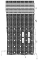
도 2aa는 일부 실시예들에 따른, 테이퍼링된 도파관에 근접하여 위치된 샘플 웰들의 행의 평면 개략도이다.
도 2ab는 도 2aa에 도시된 샘플 웰들의 행 및 테이퍼링된 도파관의 단면도이다.
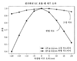
도 2b는 일부 실시예들에 따른, 모든 1024개의 샘플 웰들에 걸쳐 최소 상대 강도(minimum relative intensity)를 달성하는데 필요한 도파관에 대한 전력 입력(power input) 대 최상부 클래딩 두께(top cladding thickness)의 플롯이다.
도 2c는 일부 실시예들에 따른, 샘플 웰들의 행을 따른 강도에서의 불균일성의 양 대 테이퍼링된 도파관에 대한 최상부 클래딩 두께의 플롯이다.
도 2d는 일부 실시예들에 따른, 상대 강도 대 테이퍼링된 도파관에 결합된 샘플 웰들의 행에 대한 샘플 웰 수(sample well number)의 플롯이다.
도 2e는 일부 실시예들에 따른, 테이퍼링된 도파관에서의 전력 대 테이퍼링된 도파관에 결합된 샘플 웰들의 행에 대한 샘플 웰 수의 플롯이다.
도 2f는 일부 실시예들에 따른, 도파관 폭 대 테이퍼링된 도파관에 결합된 샘플 웰들의 행에 대한 샘플 웰 수의 플롯이다.
도 2g는 일부 실시예들에 따른, 도파관에 대한 전력 입력 대 행당 샘플 웰들의 수의 플롯이다.
도 2h는 일부 실시예에 따른, 행 효율(row efficiency) 대 행당 샘플 웰들의 수의 플롯이다.
도 3a는 일부 실시예들에 따른, 샘플 웰들의 개별 행들에 광을 전달하기 위해 다수의 도파관들이 이용되는 행 시프트 도파관 구성(row shift waveguide configuration)을 갖는 도파관 구성의 평면도이다.
도 3b는 일부 실시예들에 따른, 전력 도파관 및 행에서의 샘플 웰들의 상이한 그룹들과 광학적으로 결합하도록 위치된 다수의 도파관들을 갖는 도파관 구성의 평면도이다.
도 3c는 일부 실시예들에 따른, 전력 도파관 및 행에서의 샘플 웰들의 상이한 그룹들과 광학적으로 결합하도록 위치된 다수의 도파관들을 갖는 도파관 구성의 평면도이다.
도 3d는 일부 실시예들에 따른, 전력 도파관 및 전력 도파관과 광학적으로 결합하도록 구성된 다수의 도파관들을 갖는 도파관 구성의 평면도이다.
도 3e는 일부 실시예들에 따른, 전력 도파관 및 연속 커플러 도파관(continuous coupler waveguide)을 갖는 도파관 구성의 평면도이다.
도 3f는 일부 실시예들에 따른, 전력 도파관 및 연속 커플러 도파관을 갖는 도파관 구성의 평면도이다.
도 3g는 일부 실시예들에 따른, 최소 상대 강도를 달성하는데 필요한 연속 커플러 도파관에 대한 전력 입력 대 전력 도파관과의 초기 결합 분율(initial coupling fraction)의 플롯이다.
도 3h는 일부 실시예들에 따른, 전력 도파관 및 연속 커플러 도파관 구성에 대한, 샘플 웰들의 행을 따른 강도에서의 불균일성의 양 대 전력 도파관과의 초기 결합 분율의 플롯이다.
도 3i는 일부 실시예들에 따른, 상대 강도 대 전력 도파관 및 연속 커플러 도파관 구성에 대한 샘플 웰 수의 플롯이다.
도 3j는 일부 실시예들에 따른, 도파관에서의 전력 대 전력 도파관 및 연속 커플러 도파관 구성에 대한 샘플 웰들의 행에서의 샘플 웰 수의 플롯이다.
도 3k는 일부 실시예들에 따른, 전력 도파관과 연속 커플러 도파관 사이의 갭의 치수 대 샘플 웰 수의 플롯이다.
도 3l은 일부 실시예들에 따른, 도파관에 대한 전력 입력 대 전력 도파관 및 연속 커플러 도파관 구성에 대한 행당 샘플 웰들의 수의 플롯이다.
도 3m은 일부 실시예들에 따른, 단위 전력당 샘플 웰들의 수에 의해 측정된 행 효율 대 전력 도파관 및 연속 커플러 도파관 구성에 대한 행당 샘플 웰들의 수의 플롯이다.
도 4a는 일부 실시예들에 따른, 아포다이징된 격자 커플러(apodized grating coupler)의 단면도이다.
도 4b는 일부 실시예들에 따른, 결합 효율 대 아포다이징된 격자 커플러에 대한 최하부 클래딩 층의 두께의 플롯이다.
도 4c는 일부 실시예들에 따른, 결합 효율 대 아포다이징된 격자 커플러에 대한 측방향 치수 오차(lateral dimension error)의 플롯이다.
도 4d는 일부 실시예들에 따른, 블레이징된 격자 커플러(blazed grating coupler)의 단면도이다.
도 4e는 일부 실시예들에 따른, 블레이징된 격자 커플러에 대한 결합 효율 대 최하부 클래딩 층의 두께의 플롯이다.
도 4f는 일부 실시예들에 따른, 컬러에서의 변화가 블레이징된 격자 커플러에 대한 결합 효율에 대응하는, 파라미터 a2 대 a1을 도시하는 컬러 히트 맵(color heat map)의 그레이스케일 버전이다.
도 4g는 일부 실시예들에 따른, 컬러에서의 변화가 블레이징된 격자 커플러에 대한 결합 효율에 대응하는, 파라미터 a2 대 a1을 도시하는 컬러 히트 맵의 그레이스케일 버전이다.
도 4h는 일부 실시예들에 따른, 이중층 격자 커플러(bi-layer grating coupler)의 단면도이다.
도 4i는 일부 실시예들에 따른, 이중층 격자 커플러에 대한 결합 효율 대 최하부 클래딩 층의 두께의 플롯이다.
도 4j는 일부 실시예들에 따른, 컬러에서의 변화가 이중층 격자 커플러에 대한 결합 효율에 대응하는, 파라미터 DOffset 대 듀티 사이클을 도시하는 컬러 히트 맵의 그레이스케일 버전이다.
도 4k는 일부 실시예들에 따른, 컬러에서의 변화가 이중층 격자 커플러에 대한 결합 효율에 대응하는, 파라미터 DOffset 대 듀티 사이클을 도시하는 컬러 히트 맵의 그레이스케일 버전이다.
도 4l은 일부 실시예들에 따른, 격자 커플러의 단면도이다.
도 4m은 일부 실시예들에 따른, 격자 커플러의 단면도이다.
도 4n은 일부 실시예들에 따른, 광대역 격자 커플러의 평면도의 개략도이다.
도 4o는 일부 실시예들에 따른, 광대역 구성을 갖는 격자 커플러에 대한 대역폭 대 충전율의 플롯이다.
도 4p는 일부 실시예들에 따른, 광대역 구성을 갖는 격자 커플러에 대한 피크 파장 대 충전율의 플롯이다.
도 4q는 일부 실시예들에 따른, 광대역 구성을 갖는 격자 커플러에 대한 피크 효율 대 충전율의 플롯이다.
도 4r은 일부 실시예들에 따른, 격자 커플러의 평면도의 개략도이다.
도 4s는 일부 실시예들에 따른, 격자 커플러의 평면도의 개략도이다.
도 4t는 일부 실시예들에 따른, 격자 커플러의 평면도의 개략도이다.
도 5aa는 일부 실시예들에 따른, 통합 디바이스 및 기기의 블록도이다.
도 5ab는 일부 실시예들에 따른, 통합 디바이스를 포함하는 장치의 개략도이다.
도 5b는 일부 실시예들에 따른, 샘플 웰, 광학 도파관, 및 시간-비닝 광검출기(time-binning photodetector)를 갖는 픽셀의 개략도이다.
도 5c는 일부 실시예들에 따른, 샘플 웰 내에서 발생할 수 있는 예시적인 생물학적 반응의 개략도이다.
도 5d는 일부 실시예들에 따른, 상이한 감쇠 특성들(decay characteristics)을 갖는 2개의 상이한 형광단들(fluorophores)에 대한 방출 확률 곡선들의 플롯이다.
도 5e는 일부 실시예들에 따른, 형광 방출(fluorescent emission)의 시간-비닝 검출의 플롯이다.
도 5f는 일부 실시예들에 따른, 예시적인 시간-비닝 광검출기이다.
도 5ga는 일부 실시예들에 따른, 샘플로부터의 형광 방출의 펄스 여기 및 시간-비닝된 검출을 도시하는 개략도이다.
도 5gb는 일부 실시예들에 따른, 샘플의 반복된 펄스 여기 후의 다양한 시간 빈들에서의 축적된 형광 광자 카운트들의 히스토그램이다.
도 5ha 내지 도 5hd는 일부 실시예들에 따른, 4개의 뉴클레오티드들(nucleotides)(T, A, C, G) 또는 뉴클레오티드 유사체들(nucleotide analogs)에 대응할 수 있는 상이한 히스토그램들이다.Various aspects and embodiments of the present application will be described with reference to the following drawings. It should be understood that the drawings are not drawn to scale. Items appearing in multiple figures are denoted by the same reference number in all figures in which they appear.
1A is a cross-sectional schematic diagram of an integrated device, in accordance with some embodiments.
1B is a top schematic diagram of an integrated device, in accordance with some embodiments.
2AA is a top schematic diagram of a row of sample wells positioned proximate a tapered waveguide, in accordance with some embodiments.
FIG. 2Ab is a cross-sectional view of the row of sample wells and the tapered waveguide shown in FIG. 2AA.
2B is a plot of power input versus top cladding thickness for a waveguide required to achieve minimum relative intensity across all 1024 sample wells, according to some embodiments. .
2C is a plot of top cladding thickness for a tapered waveguide versus amount of non-uniformity in intensity along a row of sample wells, in accordance with some embodiments.
2D is a plot of relative intensity versus sample well number for a row of sample wells coupled to a tapered waveguide, in accordance with some embodiments.
2E is a plot of power in a tapered waveguide versus number of sample wells for a row of sample wells coupled to a tapered waveguide, in accordance with some embodiments.
2F is a plot of waveguide width versus number of sample wells for a row of sample wells coupled to a tapered waveguide, in accordance with some embodiments.
2G is a plot of power input to a waveguide versus number of sample wells per row, in accordance with some embodiments.
2H is a plot of row efficiency versus number of sample wells per row, in accordance with some embodiments.
3A is a top view of a waveguide configuration having a row shift waveguide configuration in which multiple waveguides are used to deliver light to individual rows of sample wells, in accordance with some embodiments.
3B is a top view of a waveguide configuration having a power waveguide and multiple waveguides positioned to optically couple with different groups of sample wells in a row, in accordance with some embodiments.
3C is a top view of a waveguide configuration having a power waveguide and multiple waveguides positioned to optically couple with different groups of sample wells in a row, in accordance with some embodiments.
3D is a top view of a waveguide configuration having a power waveguide and multiple waveguides configured to optically couple with the power waveguide, in accordance with some embodiments.
3E is a top view of a waveguide configuration with a power waveguide and a continuous coupler waveguide, in accordance with some embodiments.
3F is a top view of a waveguide configuration with a power waveguide and a continuous coupler waveguide, in accordance with some embodiments.
3G is a plot of the initial coupling fraction with a power input versus a power waveguide for a continuous coupler waveguide required to achieve a minimum relative strength, in accordance with some embodiments.
3H is a plot of initial coupling fraction with power waveguide versus amount of non-uniformity in intensity along a row of sample wells for power waveguide and continuous coupler waveguide configurations, in accordance with some embodiments.
3I is a plot of relative intensity versus sample well number for power waveguide and continuous coupler waveguide configurations, in accordance with some embodiments.
3J is a plot of power in a waveguide versus the number of sample wells in a row of sample wells for power waveguide and continuous coupler waveguide configurations, in accordance with some embodiments.
3K is a plot of the number of sample wells versus the dimension of a gap between a power waveguide and a continuous coupler waveguide, in accordance with some embodiments.
3L is a plot of power input to a waveguide versus the number of sample wells per row for a power waveguide and continuous coupler waveguide configuration, in accordance with some embodiments.
3M is a plot of row efficiency measured by number of sample wells per unit power versus number of sample wells per row for power waveguide and continuous coupler waveguide configurations, in accordance with some embodiments.
4A is a cross-sectional view of an apodized grating coupler, in accordance with some embodiments.
4B is a plot of coupling efficiency versus thickness of a bottommost cladding layer for an apodized grating coupler, in accordance with some embodiments.
4C is a plot of coupling efficiency versus lateral dimension error for an apodized grating coupler, in accordance with some embodiments.
4D is a cross-sectional view of a blazed grating coupler, in accordance with some embodiments.
4E is a plot of coupling efficiency versus thickness of the bottommost cladding layer for a brazed grating coupler, in accordance with some embodiments.
4F is a grayscale version of a color heat map showing the parameter a 2 versus a 1 , wherein a change in color corresponds to coupling efficiency for a brazed grating coupler, according to some embodiments. .
4G is a grayscale version of a color heat map showing the parameter a 2 versus a 1 , in which a change in color corresponds to coupling efficiency for a brazed grating coupler, in accordance with some embodiments.
4H is a cross-sectional view of a bi-layer grating coupler, in accordance with some embodiments.
4I is a plot of coupling efficiency versus thickness of the bottommost cladding layer for a double layer grating coupler, in accordance with some embodiments.
4J is a grayscale version of a color heat map showing Parameter D Offset versus Duty Cycle, wherein a change in color corresponds to coupling efficiency for a bilayer grating coupler, in accordance with some embodiments.
4K is a grayscale version of a color heat map showing Parameter D Offset versus Duty Cycle, wherein a change in color corresponds to coupling efficiency for a bilayer grating coupler, in accordance with some embodiments.
4L is a cross-sectional view of a grating coupler, in accordance with some embodiments.
4M is a cross-sectional view of a grating coupler, in accordance with some embodiments.
4N is a schematic diagram of a top view of a broadband grating coupler, in accordance with some embodiments.
4O is a plot of bandwidth versus fill factor for a grating coupler having a broadband configuration, in accordance with some embodiments.
4P is a plot of peak wavelength versus fill factor for a grating coupler having a broadband configuration, in accordance with some embodiments.
4Q is a plot of peak efficiency versus fill factor for a grating coupler having a broadband configuration, in accordance with some embodiments.
4R is a schematic diagram of a top view of a grating coupler, in accordance with some embodiments.
4S is a schematic diagram of a top view of a grating coupler, in accordance with some embodiments.
4T is a schematic diagram of a top view of a grating coupler, in accordance with some embodiments.
5AA is a block diagram of an integrated device and appliance, in accordance with some embodiments.
5AB is a schematic diagram of an apparatus including an integrated device, in accordance with some embodiments.
5B is a schematic diagram of a pixel having a sample well, an optical waveguide, and a time-binning photodetector, in accordance with some embodiments.
5C is a schematic diagram of an exemplary biological response that may occur within a sample well, in accordance with some embodiments.
5D is a plot of emission probability curves for two different fluorophores with different decay characteristics, in accordance with some embodiments.
5E is a plot of time-binning detection of fluorescent emission, in accordance with some embodiments.
5F is an exemplary time-binning photodetector, in accordance with some embodiments.
5G is a schematic diagram illustrating pulsed excitation and time-binned detection of fluorescence emission from a sample, in accordance with some embodiments.
5GB is a histogram of accumulated fluorescence photon counts at various time bins after repeated pulse excitation of a sample, in accordance with some embodiments.
5H-5H are different histograms that may correspond to four nucleotides (T, A, C, G) or nucleotide analogs, in accordance with some embodiments.
I. 도입 I. Introduction
본 출원의 양태들은 단일 분자들의 식별 및 핵산 서열분석을 포함하는, 샘플들을 병렬로 분석하는 것을 할 수 있는 통합 디바이스들, 기기들 및 관련 시스템들에 관한 것이다. 그러한 기기는 컴팩트하고, 운반하기 쉽고, 동작하기 쉬울 수 있어, 의사 또는 다른 제공자가 기기를 용이하게 이용할 수 있게 하고, 진료가 필요할 수 있는 원하는 위치로 기기를 수송할 수 있게 한다. 샘플의 분석은 샘플을 하나 이상의 형광 마커(fluorescent marker)로 라벨링하는 것을 포함할 수 있고, 이는 샘플을 검출하고/하거나 샘플의 단일 분자들을 식별(예를 들어, 핵산 서열분석의 일부로서 개별 뉴클레오티드 식별)하기 위해 이용될 수 있다. 형광 마커는, 형광 마커를 여기 광(excitation light)(예를 들어, 형광 마커를 여기 상태로 여기시킬 수 있는 특성 파장을 갖는 광)으로 조명하는 것에 응답하여, 여기될 수 있고, 형광 마커가 여기되는 경우, 방출 광(예를 들어, 여기 상태로부터 바닥 상태(ground state)로 복귀함으로써 형광 마커에 의해 방출되는 특성 파장을 갖는 광)을 방출한다. 방출 광의 검출은 형광 마커의 식별을 허용할 수 있고, 따라서, 형광 마커에 의해 라벨링된 샘플 또는 샘플의 분자의 식별을 허용할 수 있다. 일부 실시예들에 따르면, 기기는 대규모 병렬 샘플 분석들을 할 수 있고, 동시에 수만 개의 샘플 이상을 처리하도록 구성될 수 있다.Aspects of the present application relate to integrated devices, instruments and related systems capable of analyzing samples in parallel, including identification of single molecules and nucleic acid sequencing. Such devices may be compact, easy to transport, and easy to operate, making the devices readily available to a physician or other provider and transporting the devices to a desired location where care may be needed. Analysis of the sample may include labeling the sample with one or more fluorescent markers, which detects the sample and/or identifies single molecules in the sample (eg, identifies individual nucleotides as part of nucleic acid sequencing). ) can be used to The fluorescent marker may be excited in response to illuminating the fluorescent marker with excitation light (eg, light having a characteristic wavelength capable of excitation of the fluorescent marker into an excited state), wherein the fluorescent marker is excited When it does, it emits emission light (eg, light having a characteristic wavelength emitted by a fluorescent marker by returning from an excited state to a ground state). Detection of the emitted light may allow identification of a fluorescent marker, and thus may allow identification of a sample or molecule in the sample labeled by the fluorescent marker. According to some embodiments, the instrument may be capable of massively parallel sample analyzes and may be configured to process more than tens of thousands of samples simultaneously.
본 발명자들은 샘플을 수용하도록 구성된 샘플 웰들 및 통합 디바이스 상에 형성된 통합 광학계를 갖는 통합 디바이스, 및 통합 디바이스와 인터페이스하도록 구성된 기기를 이용하여 이러한 수의 샘플의 분석을 달성할 수 있음을 인식하고 이해하였다. 기기는 하나 이상의 여기 광원을 포함할 수 있고, 통합 디바이스는 여기 광이 통합 디바이스의 일부로서 형성된 통합 광학 컴포넌트들(예를 들어, 도파관들, 광학 커플러들, 광학 스플리터들)를 이용하여 샘플 웰들에 전달되도록 기기와 인터페이스할 수 있다. 광학 컴포넌트들은 통합 디바이스의 샘플 웰들에 걸친 조명의 균일성을 개선할 수 있고, 달리 요구될 수 있는 많은 수의 외부 광학 컴포넌트들을 감소시킬 수 있다. 또한, 본 발명자들은 통합 디바이스 상에 광검출기들을 통합하는 것이 샘플 웰들로부터의 형광 방출들의 검출 효율을 개선하고, 달리 요구될 수 있는 광 수집(light-collection) 컴포넌트들의 수를 감소시킬 수 있다는 것을 인식하고 이해하였다.The inventors have recognized and understood that analysis of this number of samples can be accomplished using an integrated device having sample wells configured to receive a sample and an integrated optics formed on the integrated device, and an instrument configured to interface with the integrated device. . The instrument can include one or more excitation light sources, wherein the integrated device is configured to allow the excitation light to reach the sample wells using integrated optical components (eg, waveguides, optical couplers, optical splitters) formed as part of the integrated device. It can interface with the device to be delivered. Optical components can improve uniformity of illumination across the sample wells of the integrated device, and can reduce the number of external optical components that would otherwise be required. In addition, the inventors recognize that integrating photodetectors on an integrated device can improve the detection efficiency of fluorescence emissions from the sample wells and reduce the number of light-collection components that may otherwise be required. and understood.
일부 실시예들에 따르면, 통합 디바이스는 어레이에 걸친 다수의 샘플들의 다중화된 분석을 허용하는 샘플 웰들의 어레이, 및 여기 광을 샘플 웰들의 어레이에 전달하도록 구성된 광학 시스템을 갖는다. 통합 디바이스의 성능은 광학 시스템을 이용하여 샘플 웰들의 어레이를 가로질러 여기 광을 전달하는 통합 디바이스의 능력에 의존할 수 있다. 추가적으로, 통합 디바이스의 성능은, 예를 들어, 비교적 일정한 강도 또는 전계 세기를 개별 샘플 웰들에 전달함으로써, 실질적으로 균일한 방식으로 개별 샘플 웰들에 여기 광을 전달하는 광학 시스템의 능력과 관련될 수 있다. 구체적으로, 광학 시스템과 연관된 성능 관련 인자들은 샘플 웰들에 의한 산란 및/또는 흡수로부터 발생하는 광학 손실, 광학 커플러(예를 들어, 외부 광원으로부터 광을 수신하도록 구성된 격자 커플러)의 결합 효율, 다수의 도파관들 사이에 여기 광을 분할하는 것으로부터 발생하는 광학 손실, 및 다수의 샘플 웰들과 개별 도파관들의 결합 효율을 포함할 수 있다.According to some embodiments, an integrated device has an array of sample wells allowing multiplexed analysis of multiple samples across the array, and an optical system configured to deliver excitation light to the array of sample wells. The performance of the integrated device may depend on the ability of the integrated device to deliver excitation light across the array of sample wells using an optical system. Additionally, the performance of the integrated device may relate to the ability of the optical system to deliver excitation light to the individual sample wells in a substantially uniform manner, for example, by delivering a relatively constant intensity or electric field strength to the individual sample wells. . Specifically, performance-related factors associated with an optical system include optical loss resulting from scattering and/or absorption by the sample wells, coupling efficiency of an optical coupler (eg, a grating coupler configured to receive light from an external light source), a number of optical losses resulting from splitting excitation light between waveguides, and coupling efficiency of individual waveguides with multiple sample wells.
통합 디바이스의 다중화 능력들을 증가시키기 위해, 어레이에서의 샘플 웰들의 수를 증가시켜, 통합 디바이스를 이용하는 동안 임의의 특정한 시간에 더 많은 샘플들을 분석하는 능력을 허용하는 것이 바람직할 수 있다. 통합 디바이스가 샘플 웰들의 수를 증가시킴으로써 스케일링됨에 따라, 이들 인자들 중 하나 이상 때문에 통합 디바이스의 성능에서의 도전과제가 발생할 수 있다. 예를 들어, 샘플 웰들의 행은, 광이 도파관을 따라 전파될 때, 행에서의 샘플 웰들이 광의 일부를 수신하도록, 광학 시스템의 도파관에 결합함으로써 광을 수신할 수 있다. 광학 손실은 개별 샘플 웰들이 광을 산란 및/또는 흡수하는 것으로부터 발생할 수 있으며, 이는 (예를 들어, 도파관의 광학 입력 단부로부터 먼) 행에서의 마지막 샘플 웰이 행에서의 제1 샘플 웰(예를 들어, 도파관의 광학 입력 단부에 근접한 샘플 웰)보다 낮은 강도 또는 전계 세기를 수신하는 것을 누적적으로 초래할 수 있다. 그러한 광학 손실은 통합 디바이스를 이용하여 수행되는 측정들의 신호 대 잡음비에 영향을 줄 수 있다. 더 많은 샘플 웰들이 어레이에 추가됨에 따라, 이들 광학 손실들은 신호 대 잡음비에서의 추가의 감소를 초래할 수 있고, 이것은 수행된 분석의 품질 및 신뢰성에 영향을 미칠 수 있다.To increase the multiplexing capabilities of the integrated device, it may be desirable to increase the number of sample wells in the array, allowing the ability to analyze more samples at any particular time while using the integrated device. As an integrated device scales by increasing the number of sample wells, one or more of these factors may create a challenge in the performance of the integrated device. For example, a row of sample wells may receive light by coupling to a waveguide of an optical system such that as the light propagates along the waveguide, the sample wells in the row receive a portion of the light. Optical loss may result from individual sample wells scattering and/or absorbing light, such that the last sample well in a row (e.g., far from the optical input end of the waveguide) becomes the first sample well in the row ( For example, it may cumulatively result in receiving a lower intensity or electric field strength than a sample well proximate to the optical input end of the waveguide). Such optical loss can affect the signal-to-noise ratio of measurements performed using the integrated device. As more sample wells are added to the array, these optical losses can result in a further decrease in signal-to-noise ratio, which can affect the quality and reliability of the analysis performed.
따라서, 본 출원의 양태들은 샘플 웰들의 어레이 사이의 광의 개선된 분배를 허용할 수 있는 통합 디바이스의 광학 시스템에 포함하기 위한 광학 컴포넌트들 및 특정 배열들에 관한 것이다. 이들 광학 컴포넌트들 및 배열들은 동일한 행 내의 샘플 웰들을 포함하는 개별 샘플 웰들이 유사한 강도 및/또는 전계 세기를 수용하도록 실질적으로 균일한 방식으로 광을 전달하는 것을 허용할 수 있다. 본 명세서에 설명된 광학 컴포넌트들 및 배열들은 어레이에서의 더 많은 수의 샘플 웰들을 갖는 통합 디바이스들의 구현 뿐만 아니라, 어레이에 걸쳐 샘플들을 분석하는데 있어서 원하는 성능을 허용할 수 있다.Accordingly, aspects of the present application relate to optical components and specific arrangements for inclusion in an optical system of an integrated device that can allow for improved distribution of light between an array of sample wells. These optical components and arrangements may allow for transmitting light in a substantially uniform manner such that individual sample wells, including sample wells in the same row, receive similar intensity and/or electric field strength. The optical components and arrangements described herein may allow for the desired performance in analyzing samples across the array, as well as implementation of integrated devices having a greater number of sample wells in the array.
어레이에서의 샘플 웰들의 수를 스케일 업(scaling up)하는 것의 일부로서 추가의 고려사항들은 제조 비용들 및 제약들을 포함할 수 있다. 따라서, 본 출원의 양태들은 (예를 들어, 제조 단계들의 수 또는 복잡성을 감소시킴으로써) 제조 비용들 및 제약들을 고려하면서 결과적인 통합 디바이스가 원하는 광학 성능을 달성하는 것을 허용하는 광학 컴포넌트들 및 시스템들에 관한 것이다.Additional considerations as part of scaling up the number of sample wells in the array may include manufacturing costs and constraints. Accordingly, aspects of the present application provide optical components and systems that allow the resulting integrated device to achieve desired optical performance while considering manufacturing costs and constraints (eg, by reducing the number or complexity of manufacturing steps). is about
본 출원에 설명된 바와 같은 광학 시스템을 위한 기술들은 여기 광을 샘플 웰들의 어레이에 전달하는 것과 관련하여 논의되지만, 이들 기술 중 하나 이상은 광자 디바이스 내의 광자 요소들의 어레이에 광을 분배하는 것을 수반하는 다른 맥락들에서, 단독으로 또는 조합하여 이용될 수 있다는 것이 이해되어야 한다. 예를 들어, 본 출원의 기술들은 센서들의 어레이와 같은 광학 컴포넌트들의 어레이로 구현될 수 있다. 추가적으로, 본 명세서에 설명된 기술들은 생물학적 또는 화학적 샘플들을 분석하는 맥락으로 제한되지 않고, 오히려 실질적으로 균일한 방식으로 많은 광자 요소들 사이에 광을 분배하는 것이 요구되는 응용들에서 구현될 수 있다는 것을 이해해야 한다.While techniques for an optical system as described herein are discussed with respect to delivering excitation light to an array of sample wells, one or more of these techniques involve distributing light to an array of photonic elements within a photonic device. It should be understood that in other contexts, they may be used alone or in combination. For example, the techniques herein may be implemented with an array of optical components, such as an array of sensors. Additionally, it is noted that the techniques described herein are not limited to the context of analyzing biological or chemical samples, but rather can be implemented in applications where it is desired to distribute light among many photonic elements in a substantially uniform manner. have to understand
통합 디바이스의 광학 시스템은 다음의 3개의 섹션들을 갖는 것으로 고려될 수 있다: (1) 외부 광원(예를 들어, 기기의 여기 광원)으로부터의 광을 통합 디바이스의 도파관에 결합하는 격자 커플러; (2) (예를 들어, 광학 스플리터들의 조합을 통해) 통합 디바이스 전체에 걸쳐 분포된 개별 도파관들 사이에 격자 커플러로부터 수신된 광을 분할하는 광학 라우팅 네트워크(optical routing network); (3) 통합 디바이스의 어레이에서의 샘플 웰을 조명하도록 구성된 어레이 도파관들. 통합 디바이스의 성능은 광학 시스템의 이들 섹션들 중 임의의 하나의 광학 성능에 의존할 수 있다. 따라서, 본 출원의 양태들은 전체 광학 시스템의 이들 섹션들 중 하나 이상에 관한 것이다.An optical system of an integrated device may be considered to have three sections: (1) a grating coupler that couples light from an external light source (eg, an excitation light source of an instrument) to a waveguide of the integrated device; (2) an optical routing network that splits the light received from the grating coupler between individual waveguides distributed throughout the integrated device (eg, via a combination of optical splitters); (3) Array waveguides configured to illuminate a sample well in the array of the integrated device. The performance of the integrated device may depend on the optical performance of any one of these sections of the optical system. Accordingly, aspects of the present application relate to one or more of these sections of the overall optical system.
본 출원의 일부 양태들은 외부 광원으로부터의 광을 광학 시스템의 다른 광학 컴포넌트들에 결합함에 있어서 원하는 광학 효율을 허용할 수 있는 격자 커플러 구성들에 관한 것이다. 일부 경우들에서, 특정 격자 커플러 구성은 광학 효율을 개선하도록 달리 작용할 수 있는 다른 광학 컴포넌트를 통합할 필요성을 감소시킬 수 있다. 예를 들어, 일부 격자 커플러들은, 격자 커플러를 통과하는 광을 다시 격자 커플러로 반사하도록 위치된 반사 층을 갖지 않고 원하는 광학 효율이 달성되는 것을 허용할 수 있고, 여기서, 그러한 반사 층은 그렇지 않은 경우 다른 격자 커플러들이 동일한 원하는 광학 효율을 달성하는데 필요할 수 있다.Some aspects of the present application relate to grating coupler configurations that can allow for a desired optical efficiency in coupling light from an external light source to other optical components of an optical system. In some cases, a particular grating coupler configuration may reduce the need to incorporate other optical components that may otherwise act to improve optical efficiency. For example, some grating couplers may allow a desired optical efficiency to be achieved without a reflective layer positioned to reflect light that passes through the grating coupler back to the grating coupler, where such a reflective layer would otherwise Other grating couplers may be needed to achieve the same desired optical efficiency.
통합 디바이스의 전체 성능에 영향을 미칠 수 있는 또 다른 양태는, 외부 광원을 격자 커플러에 정렬하는 능력이며, 외부 광원을 다수의 통합 디바이스들에 정렬하는 많은 반복들에 걸쳐 정렬을 수행하는 용이성을 포함한다. 일부 경우들에서, 외부 광원을 격자 커플러에 정렬하는 것은 격자 커플러에 입사하는 특정 범위의 각도들 내에서 여기 광의 빔을 정렬하는 것을 수반할 수 있다. 일부 격자 커플러 구성들은 제조 공차(fabrication tolerance)를 거의 또는 전혀 갖지 않을 수 있고, 여기서, 다수의 통합 디바이스들 위에서의 제조는, 이들 디바이스들이 상이한 범위의 각도들에서 입사 광과 결합하도록 구성된 격자 커플러들을 갖게 할 수 있다. 이러한 격자 커플러 구성들에 대한 제조 공차가 거의 없거나 전혀 없는 것은, 하나의 디바이스로부터 다른 디바이스로 전이할 때 광학 정렬을 수행하는데 필요한 시간량을 증가시킴으로써 디바이스들이 분석을 위해 이용될 때 외부 광원의 정렬을 수행할 때 도전과제들을 초래할 수 있다. 본 발명자들은, 다수의 층들 및/또는 비주기적 격자들을 갖는 격자 커플러가, 격자 커플러와 정렬된 것으로 간주되는 입사 광 빔에 대한 더 넓은 범위의 각도들을 수용하고, 원하는 결합 효율을 달성할 수 있으므로, 다수의 통합 디바이스들에 걸친 제조 변동에 대해 더 내성이 있는 이점을 제공할 수 있다는 것을 인식하고 이해하였다.Another aspect that may affect the overall performance of an integrated device is the ability to align an external light source to a grating coupler, including the ease of performing alignment over many iterations of aligning an external light source to multiple integrated devices. do. In some cases, aligning the external light source to the grating coupler may involve aligning the beam of excitation light within a certain range of angles incident on the grating coupler. Some grating coupler configurations may have little or no fabrication tolerance, where fabrication on multiple integrated devices requires that these devices be configured to couple grating couplers with incident light at a different range of angles. can have it Little or no manufacturing tolerances for these grating coupler configurations reduce the alignment of external light sources when devices are used for analysis by increasing the amount of time required to perform optical alignment when transitioning from one device to another. It can present challenges when performing. The inventors have found that a grating coupler with multiple layers and/or aperiodic gratings can accommodate a wider range of angles for an incident light beam considered aligned with the grating coupler and achieve the desired coupling efficiency, It has been recognized and understood that it may provide the advantage of being more resistant to manufacturing variations across multiple integrated devices.
일부 실시예들에서, 통합 광자 디바이스는 표면에 실질적으로 평행한 평면에 대해 비대칭 재료 구조체들을 갖는 격자 커플러를 포함할 수 있다. 재료 구조체들은 평면에 실질적으로 평행한 방향으로 서로 측방향으로 오프셋된 2개 이상의 재료 층들을 포함할 수 있다. 재료 구조체들은 격자 커플러의 하나 이상의 층을 적어도 부분적으로 에칭함으로써 형성될 수 있다. 일부 실시예들에서, 재료 구조체들은 통합 광자 디바이스의 표면에 실질적으로 수직인 평면에 대해 비대칭일 수 있다. 일부 실시예들에서, 2개 이상의 재료 층들은 서로 접촉할 수 있다. 일부 실시예들에서, 2개 이상의 재료들은 소정 거리만큼 서로 이격될 수 있다. 일부 실시예들에서, 격자 커플러는 블레이징된 격자 커플러이다.In some embodiments, the integrated photonic device can include a grating coupler having material structures asymmetric with respect to a plane substantially parallel to the surface. The material structures may include two or more material layers laterally offset from one another in a direction substantially parallel to the plane. The material structures may be formed by at least partially etching one or more layers of the grating coupler. In some embodiments, the material structures may be asymmetric with respect to a plane substantially perpendicular to the surface of the integrated photonic device. In some embodiments, two or more layers of material may contact each other. In some embodiments, two or more materials may be spaced apart from each other by a distance. In some embodiments, the grating coupler is a brazed grating coupler.
일부 실시예들에서, 격자 커플러는 가변 충전율로 서로 이격된 재료 구조체를 갖는 아포다이징된 격자 커플러이다. 재료 구조체들은 가변 폭들을 가질 수 있다. 재료 구조체들은 가변 폭들을 갖는 갭들에 의해 서로 이격될 수 있다. 유전체 재료가 갭들에 형성될 수 있다.In some embodiments, the grating coupler is an apodized grating coupler having material structures spaced apart from each other with a variable fill factor. The material structures may have variable widths. The material structures may be spaced apart from each other by gaps having variable widths. A dielectric material may be formed in the gaps.
본 출원의 일부 양태들은 실질적으로 균일한 방식으로 다수의 샘플 웰들 또는 다른 광자 요소들을 조명하는 것을 허용할 수 있는 도파관 구성들에 관한 것이다. 그러한 도파관 구성들은 샘플 웰 어레이의 개별 행들에 더 많은 샘플 웰들(예를 들어, 행에 2,000개보다 많은 샘플 웰들)을 갖는 통합 디바이스를 허용할 수 있다. 본 발명자들은 샘플 웰들의 행과 결합하기 위해 다수의 도파관들을 이용하는 것이, 광학 입력 단부로부터 멀리 위치한 행에서의 샘플 웰들에 대한 광학 손실들의 영향을 감소시키는 것을 포함하여, 행을 조명하기 위해 단일 도파관만을 이용하는 것과 연관된 제한들을 극복할 수 있다는 것을 인식하고 이해하였다. 따라서, 일부 실시예들은 샘플 웰들의 행과 광학적으로 결합하도록 구성된 다수의 도파관들을 갖는 통합 디바이스에 관한 것이다. 광학 결합 기술들이 샘플 웰들의 행과 관련하여 설명되지만, 이러한 기술들은 샘플 웰들의 다른 배열들(예를 들어, 샘플 웰들의 열)과 광학적으로 결합하는데 이용될 수 있다는 것을 이해해야 한다.Some aspects of the present application relate to waveguide configurations that may allow to illuminate multiple sample wells or other photonic elements in a substantially uniform manner. Such waveguide configurations may allow for an integrated device with more sample wells in individual rows of a sample well array (eg, more than 2,000 sample wells in a row). We believe that using multiple waveguides to couple with a row of sample wells includes reducing the effect of optical losses on sample wells in a row located away from the optical input end, including reducing the effect of optical losses on a row of sample wells. It was recognized and understood that limitations associated with its use could be overcome. Accordingly, some embodiments relate to an integrated device having a plurality of waveguides configured to optically couple with a row of sample wells. Although optical coupling techniques are described with respect to a row of sample wells, it should be understood that these techniques can be used to optically couple other arrangements of sample wells (eg, a column of sample wells).
일부 실시예들은 동일한 행 내의 샘플 웰들의 상이한 그룹들과 광학적으로 결합하도록 구성된 다수의 도파관들을 갖는 행 시프트 도파관 구성에 관한 것이다. 일부 실시예들에서, 행에서의 샘플 웰들 중 일부는 상이한 도파관들 사이의 전이 영역에 위치될 수 있고, 도파관들 중 하나와 광학적으로 결합하도록 구성된 다른 샘플 웰들보다 적은 광학 전력을 수신할 수 있다.Some embodiments relate to a row shift waveguide configuration having multiple waveguides configured to optically couple with different groups of sample wells in the same row. In some embodiments, some of the sample wells in a row may be located in a transition region between different waveguides and may receive less optical power than other sample wells configured to optically couple with one of the waveguides.
일부 실시예들은 전력 도파관, 및 행에서의 샘플 웰들 및 전력 도파관과 광학적으로 결합하도록 구성된 하나 이상의 도파관을 갖는 도파관 구성들에 관한 것이다. 일부 실시예들에서, 하나 이상의 도파관은 전력 스플리터를 통해 전력 도파관과 광학적으로 결합할 수 있다. 일부 실시예들에서, 도파관은 도파관의 길이를 따라 전력 도파관과 약하게 결합하도록 구성될 수 있다. 그러한 실시예들에서, 전력 도파관은 광이 도파관을 따라 전파함에 따라 광학 손실들을 보상할 수 있다.Some embodiments relate to a power waveguide and waveguide configurations having one or more waveguides configured to optically couple with the power waveguide and sample wells in a row. In some embodiments, one or more waveguides may optically couple with the power waveguide via a power splitter. In some embodiments, the waveguide may be configured to weakly couple with the power waveguide along the length of the waveguide. In such embodiments, the power waveguide may compensate for optical losses as light propagates along the waveguide.
위에서 설명된 양태들 및 실시예들은 물론, 추가의 양태들 및 실시예들이 이하에서 더 설명된다. 이러한 양태들 및/또는 실시예들은 개별적으로, 모두 함께, 또는 둘 이상의 임의의 조합으로 이용될 수 있으며, 이는 본 출원이 이러한 점에서 제한되지 않기 때문이다.Aspects and embodiments described above, as well as additional aspects and embodiments are further described below. These aspects and/or embodiments may be used individually, all together, or in any combination of two or more, as the present application is not limited in this respect.
II. 통합 디바이스 II. integrated device
A. 개요 A. Overview
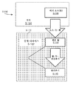
픽셀들(1-112)의 행을 나타내는 통합 디바이스(1-102)의 단면 개략도가 도 1a에 도시되어 있다. 통합 디바이스(1-102)는 결합 영역(1-201), 라우팅 영역(1-202), 및 픽셀 영역(1-203)을 포함할 수 있다. 본 명세서에서 논의되는 바와 같이, 통합 디바이스의 광학 시스템은 통합 디바이스의 영역들(1-201, 1-202 및 1-203) 내에 위치될 수 있는 상이한 타입들의 광학 컴포넌트들을 포함할 수 있다. 결합 영역(1-201)은, (파선 화살표로 도시된) 여기 광을 수신하고, 여기 광을 라우팅 영역(1-202)에서의 하나 이상의 광학 컴포넌트에 전파하도록 구성될 수 있는 격자 커플러(1-216)를 포함할 수 있다. 라우팅 영역(1-202)은 광을 픽셀 영역(1-203)으로 전파하도록 구성된 다수의 도파관들(1-220) 사이에 광을 분할하도록 구성된 광학 라우팅 네트워크를 포함할 수 있다. 픽셀 영역(1-203)은, (파선 화살표로 도시된) 여기 광이 통합 디바이스(1-102)에 결합되는, 결합 영역(1-201)으로부터 분리된 위치에서의 표면 상에 위치된 샘플 웰들(1-108)을 갖는 복수의 픽셀들(1-112)을 포함할 수 있다. 샘플 웰들(1-108)은 금속 층(들)(1-106)을 통해 형성될 수 있다. 점선 직사각형에 의해 도시된 하나의 픽셀(1-112)은 샘플 웰(1-108) 및 하나 이상의 광검출기(1-110)를 갖는 광검출기 영역을 포함하는 통합 디바이스(1-102)의 영역이다.A cross-sectional schematic diagram of an integrated device 1-102 representing a row of pixels 1-112 is shown in FIG. 1A . The integrated device 1-102 may include a coupling region 1-201 , a routing region 1-202 , and a pixel region 1-203 . As discussed herein, the optical system of the integrated device may include different types of optical components that may be located within regions 1-201 , 1-202 and 1-203 of the integrated device. Coupling region 1-201 is a grating coupler 1-201, which may be configured to receive excitation light (shown by dashed arrows) and propagate the excitation light to one or more optical components in routing region 1-202. 216) may be included. Routing region 1-202 may include an optical routing network configured to split light between a plurality of waveguides 1-220 configured to propagate light to pixel region 1-203. Pixel region 1-203 includes sample wells located on the surface at a location separate from coupling region 1-201 where excitation light (shown by dashed arrows) is coupled to integrated device 1-102 . It may include a plurality of pixels 1-112 having (1-108). Sample wells 1-108 may be formed through metal layer(s) 1-106. One pixel 1-112, shown by the dashed rectangle, is an area of an integrated device 1-102 comprising a sample well 1-108 and a photodetector region having one or more photodetectors 1-110. .
도 1a는 여기 광의 빔을 결합 영역(1-201)에 결합하고, 여기 광을 샘플 웰들(1-108)에 지향시킴으로써, 통합 디바이스를 통한 (파선들로 도시된) 여기 광의 경로를 도시한다. 도 1a에 도시된 샘플 웰들(1-108)의 행은 도파관(1-220)과 광학적으로 결합하도록 위치될 수 있다. 여기 광은 샘플 웰 내에 위치한 샘플을 조명할 수 있다. 샘플은 여기 광에 의해 조명되는 것에 응답하여 여기 상태에 도달할 수 있다. 샘플이 여기 상태에 있을 때, 샘플은 방출 광을 방출하고, 이는 샘플 웰과 연관된 하나 이상의 광검출기에 의해 검출될 수 있다. 도 1a는 샘플 웰(1-108)로부터 픽셀(1-112)의 광검출기(들)(1-110)로의 (실선으로 도시된) 방출 광의 경로를 개략적으로 도시한다. 픽셀(1-112)의 광검출기(들)(1-110)는 샘플 웰(1-108)로부터의 방출 광을 검출하도록 구성되고 위치될 수 있다. 적절한 광검출기들의 예들은 발명의 명칭이 "INTEGRATED DEVICE FOR TEMPORAL BINNING OF RECEIVED PHOTONS"인 미국 특허 출원 재14/821,656호에 기술되어 있으며, 그러한 특허 출원 전체가 본 명세서에 참고로 포함된다. 적절한 광검출기들의 추가의 예들은 2017년 12월 22일자로 출원된, 발명의 명칭이 "INTEGRATED PHOTODETECTOR WITH DIRECT BINNING PIXEL"인 미국 특허 출원 제15/852,571호에 기술되어 있으며, 그러한 특허 출원 전체가 본 명세서에 참고로 포함된다. 개별 픽셀(1-112)에 대해, 샘플 웰(1-108) 및 그 각각의 광검출기(들)(1-110)는 공통 축을 따라(도 1a에 도시된 y 방향을 따라) 정렬될 수 있다. 이러한 방식으로, 광검출기(들)는 픽셀(1-112) 내의 샘플 웰과 중첩할 수 있다.1A illustrates the path of excitation light (shown in dashed lines) through an integrated device by coupling a beam of excitation light to coupling region 1-201 and directing the excitation light to sample wells 1-108. The row of sample wells 1-108 shown in FIG. 1A may be positioned to optically couple with the waveguide 1-220. The excitation light may illuminate a sample positioned within the sample well. The sample may reach an excited state in response to being illuminated by the excitation light. When the sample is in an excited state, the sample emits emission light, which can be detected by one or more photodetectors associated with the sample well. FIG. 1A schematically shows the path of emitted light (shown in solid lines) from the sample well 1-108 to the photodetector(s) 1-110 of the pixel 1-112. Photodetector(s) 1-110 of pixel 1-112 may be configured and positioned to detect emission light from sample well 1-108. Examples of suitable photodetectors are described in U.S. Patent Application Serial No. 14/821,656 entitled "INTEGRATED DEVICE FOR TEMPORAL BINNING OF RECEIVED PHOTONS," which is incorporated herein by reference in its entirety. Additional examples of suitable photodetectors are described in U.S. Patent Application Serial No. 15/852,571, entitled “INTEGRATED PHOTODETECTOR WITH DIRECT BINNING PIXEL,” filed December 22, 2017, the entirety of which is incorporated herein by reference. The specification is incorporated by reference. For individual pixels 1-112, sample wells 1-108 and their respective photodetector(s) 1-110 may be aligned along a common axis (along the y-direction shown in FIG. 1A ). . In this way, the photodetector(s) may overlap the sample wells in pixels 1-112.
픽셀들의 5개 행들을 나타내는 통합 디바이스(1-102)의 평면도가 도 1b에 도시되어 있다. 도 1b에 도시된 바와 같이, 샘플 웰(1-108a)과 샘플 웰(1-108b)은 동일한 행에 있고, 샘플 웰(1-108c)과 샘플 웰(1-108d)은 동일한 행에 있다. 본 출원의 양태들은 결합 영역(1-201)에 입사하는 여기 광을 수신하고, 여기 광을 샘플 웰들(1-108)의 어레이에 전파하기 위한 기술들에 관한 것이다. 이러한 기술들은, 결합 영역(1-201)으로부터 개별 샘플 웰들(1-108)로 여기 광을 전달하기 위해, 결합 영역(1-201)에 위치된 하나 이상의 광학 격자 커플러, 및 라우팅 영역(1-202) 및/또는 픽셀 영역(1-203)에 위치된 도파관 아키텍처를 갖는 것을 포함할 수 있다.A top view of an integrated device 1-102 representing five rows of pixels is shown in FIG. 1B . 1B , sample wells 1-108a and sample wells 1-108b are in the same row, and sample wells 1-108c and sample wells 1-108d are in the same row. Aspects of the present application relate to techniques for receiving excitation light incident on coupling region 1-201 and propagating the excitation light to an array of sample wells 1-108. These techniques include one or more optical grating couplers positioned in the coupling region 1-201, and a routing region 1-108, to deliver excitation light from the coupling region 1-201 to the individual sample wells 1-108. 202) and/or having a waveguide architecture located in pixel regions 1-203.
B. 도파관 아키텍처 B. Waveguide Architecture
일부 실시예들은 하나 이상의 테이퍼링된 도파관을 갖는 통합 디바이스에 관한 것이다. 테이퍼링된 도파관은 도파관의 길이를 따라 그리고 도파관을 통한 광 전파의 방향으로 변하는 하나 이상의 치수를 갖는다. 예를 들어, 도파관의 길이를 따라 변하는 폭을 갖는 도파관은 테이퍼링된 도파관으로서 간주될 수 있다. 테이퍼링된 도파관을 따라 전파되는 광의 특성들은 테이퍼링된 도파관의 변하는 하나 이상의 치수에 따라 변할 수 있다. 샘플 웰들의 어레이 사이에 실질적으로 균일한 방식으로 광을 분배하는 맥락에서, 테이퍼링된 도파관은 테이퍼링된 도파관에 근접하여 위치된 샘플 웰들의 그룹 사이에 유사한 양의 광 강도를 제공하는 기술로서 구현될 수 있다. 통합 디바이스의 일부 실시예들에서, 테이퍼링된 도파관은 샘플 웰 어레이에서의 샘플 웰들의 행과 결합하도록 위치할 수 있으며, 여기서 도파관의 테이퍼링은 행에서의 개별 샘플 웰들에서 유사한 양의 광 강도를 허용하도록 적절하게 치수화된다. 테이퍼링된 도파관은 행에서의 샘플 웰들과 소멸파에 의해(evanescently) 결합할 수 있고, 도파관의 폭은 도파관의 광 입력 단부에 더 가까운 더 약한 소멸파 필드(evanescent field) 및 도파관의 광 입력 단부에 대해 더 먼 쪽의 더 강한 소멸파 필드를 제공하도록 테이퍼링될 수 있다. 그러한 도파관 구성은 일정한 폭을 갖는 도파관이 이용된 경우보다 도파관에 의해 샘플 웰들의 행 사이에 전달되는 더 균일한 여기 강도를 허용할 수 있다.Some embodiments relate to an integrated device having one or more tapered waveguides. The tapered waveguide has one or more dimensions that vary along the length of the waveguide and in the direction of light propagation through the waveguide. For example, a waveguide having a width that varies along the length of the waveguide may be considered a tapered waveguide. The properties of light propagating along the tapered waveguide may vary with one or more varying dimensions of the tapered waveguide. In the context of distributing light in a substantially uniform manner between an array of sample wells, a tapered waveguide may be implemented as a technique that provides a similar amount of light intensity between a group of sample wells positioned proximate the tapered waveguide. have. In some embodiments of the integrated device, the tapered waveguide may be positioned to engage a row of sample wells in a sample well array, wherein the tapering of the waveguide allows for a similar amount of light intensity in individual sample wells in the row. appropriately dimensioned. The tapered waveguide can evanescently couple with the sample wells in a row, the width of the waveguide being the weaker evanescent field closer to the light input end of the waveguide and the light input end of the waveguide may be tapered to provide a stronger evanescent field on the far side of the Such a waveguide configuration may allow for a more uniform excitation intensity transferred between rows of sample wells by the waveguide than if a waveguide having a constant width was used.
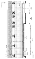
도 2aa는 테이퍼링된 도파관(2-220)을 따라 행으로 샘플 웰들(1-108e 및 1-108f)을 포함하는 샘플 웰들의 평면도를 도시하며, 여기서 광은 도 2aa에 도시된 화살표에 대응하는 측에서 도파관(2-220)에 입력되고 z 방향을 따라 전파된다. 도 2aa에 도시된 바와 같이, 테이퍼링된 도파관(2-220)의 폭은 샘플 웰들의 행을 따라 변하고, 도파관(2-220)은 입력 측으로부터 먼 쪽보다 (화살표에 더 가까운) 입력 측에 근접한 쪽에서 더 큰 폭을 갖는다. 따라서, 샘플 웰(1-108e)은 샘플 웰(1-108f)이 그 위에 위치되는 도파관(2-220)의 영역보다 큰 폭을 갖는 도파관(2-220)의 영역 위에 위치된다. 도 2ab는 도 2aa에 도시된 샘플 웰들(1-108)의 행의 단면도이고, 광학 모드 프로파일이 테이퍼링된 도파관(2-220)의 길이를 따라(z 방향을 따라) 어떻게 변하는지를 도시한다. 변하는 광학 모드 프로파일들은 광이 테이퍼링된 도파관(2-220)을 따라 전파될 때 샘플 웰의 최하부에 근접한 조명 영역에 도달하는 강도의 양에 영향을 미친다. 특히, 샘플 웰(1-108e)에 근접한 테이퍼링된 도파관(2-220)의 더 큰 폭은 샘플 웰(1-108e)의 조명 영역 내에서 더 작은 강도를 제공하는 반면, 샘플 웰(1-108f)에 근접한 테이퍼링된 도파관(2-220)의 더 작은 폭은 샘플 웰(1-108f)의 조명 영역 내에서 더 큰 강도를 갖는다. 일부 실시예들에서, 최상부 클래딩 층(2-222)의 하나 이상의 특성(예를 들어, 두께, 재료)은 도파관(2-220)의 테이퍼 형상에 영향을 미칠 수 있다.2AA shows a top view of sample wells comprising sample wells 1-108e and 1-108f in rows along a tapered waveguide 2-220, where the light is on the side corresponding to the arrow shown in FIG. 2AA. is input to the waveguide (2-220) and propagates along the z direction. As shown in Figure 2aa, the width of tapered waveguide 2-220 varies along the row of sample wells, with waveguide 2-220 closer to the input side (closer to the arrow) than far from the input side. has a larger width on the side. Thus, sample wells 1-108e are positioned over a region of waveguide 2-220 that has a greater width than the region of waveguide 2-220 over which sample wells 1-108f are positioned. FIG. 2Ab is a cross-sectional view of the row of sample wells 1-108 shown in FIG. 2AA and shows how the optical mode profile changes along the length (along the z-direction) of the tapered waveguide 2-220. Varying optical mode profiles affect the amount of intensity that reaches the illumination region proximate to the bottom of the sample well as light propagates along the tapered waveguide 2-220. In particular, the larger width of the tapered waveguide 2-220 proximate the sample wells 1-108e provides less intensity within the illumination region of the sample wells 1-108e, while the sample wells 1-108f ), the smaller width of the tapered waveguide 2-220 has a greater intensity within the illumination region of the sample well 1-108f. In some embodiments, one or more properties (eg, thickness, material) of top cladding layer 2-222 may affect the tapered shape of waveguide 2-220 .
추가적으로, 테이퍼링된 도파관은 도파관에 근접하여 위치된 샘플 웰들에 의한 흡수 및 산란과 연관된 광학 손실을 포함하는, 도파관의 길이를 따른 광학 손실을 고려하는 구성을 가질 수 있다. 일부 실시예들에서, 도파관의 테이퍼링의 구성은, 광이 도파관을 따라 전파될 때 광학 전력 손실로부터 발생하는 샘플 웰들에 의해 수신된 광의 강도에서의 변화가 감소되거나 방지되도록, 샘플 웰 어레이에 걸쳐 원하는 전력 효율을 제공할 수 있다. 그러한 구성들은 샘플 웰 어레이를 가로지르는 여기 광의 불균일한 전달에 기여하는 인자로서의 광학 전력 손실이 효과적으로 제거되게 할 수 있다.Additionally, the tapered waveguide can be configured to account for optical losses along the length of the waveguide, including optical losses associated with absorption and scattering by sample wells positioned proximate the waveguide. In some embodiments, the configuration of the tapering of the waveguide is such that a change in intensity of light received by the sample wells that results from optical power loss as the light propagates along the waveguide is reduced or prevented, such that a change is desired across the sample well array. It can provide power efficiency. Such configurations can effectively eliminate optical power loss as a factor contributing to non-uniform transmission of excitation light across the sample well array.
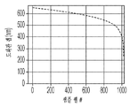
특히, 도파관에서의 전력은 함수 ![]()
![]()
본 명세서에 설명된 일부 실시예들에 따르면, "실질적으로 균일한 강도"는 도파관과 결합하도록 위치된 샘플 웰에 의해 수신된 최고 강도와 도파관과 결합하도록 위치된 샘플 웰에 의해 수신된 최저 강도를 관련시킴으로써 특정 도파관에 대해 결정될 수 있다. 일부 실시예들에서, 도파관에 결합하는 샘플 웰들의 그룹에 대한 "실질적으로 균일한 강도"는 그룹에서의 샘플 웰들에 의해 수신된 최고 강도 대 최저 강도의 비율이 대략 1과 동일한(예를 들어, 1±5%와 동일한, 1±10%와 동일한) 것에 대응할 수 있다.According to some embodiments described herein, “substantially uniform intensity” is defined as the highest intensity received by a sample well positioned to engage the waveguide and the lowest intensity received by a sample well positioned to engage the waveguide. It can be determined for a particular waveguide by associating it. In some embodiments, a “substantially uniform intensity” for a group of sample wells that couple to a waveguide is such that the ratio of the highest to the lowest intensity received by the sample wells in the group is approximately equal to (e.g., equal to 1±5%, equal to 1±10%).
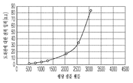
최상부 클래딩 층(2-222)의 두께는 행에서의 샘플 웰들에 의해 수신된 강도에서의 균일성의 정도에 영향을 미칠 수 있다. 도 2b 및 도 2c는 최상부 클래딩 두께가 변화고, 비선형 테이퍼를 갖는 도파관이 1024개의 샘플 웰들의 행에 대한 최소의 상대 강도를 달성하도록 설계된 시뮬레이션 결과들을 도시한다. 도파관은 120nm의 두께, 300nm의 최소 폭 값, 및 1300nm의 최대 폭 값을 갖는다. 샘플 웰들은 300nm의 깊이를 갖는다. 도 2b는 모든 1024개의 샘플 웰들에 걸쳐 최소 상대 강도를 달성하는데 필요한 도파관에 대한 전력 입력 대 최상부 클래딩 두께의 플롯을 도시한다. 도 2b에 도시된 플롯은, 도파관에 대한 입력 전력이 최소인 경우, 380nm와 400nm 사이의 최상부 클래딩 층(2-222)의 두께에 대한 최적 값이 어떻게 존재하는지를 도시한다. 도 2c는 샘플 웰들의 행을 따른 강도에서의 불균일성의 양 대 최상부 클래딩 두께의 플롯을 도시하며, 여기서 불균일성은 샘플 웰에서의 최저 강도에 대한 샘플 웰에서의 최고 강도의 비율에 대응한다. 1과 동일한 불균일성 값은 최고 강도 및 최저 강도 값들이 동일한 것에 대응하고, 따라서 행에서의 모든 샘플 웰들에서 균일한 강도가 존재하는 시나리오이다. 도 2b 및 도 2c 둘다를 참조하면, 입력 전력, 최상부 클래딩 두께, 및 불균일성 사이에 균형이 있다. 특히, 최상부 클래딩 층이 그의 최적 값보다 두꺼울 때, 1과 동일한 불균일성이 달성될 수 있지만, 최상부 클래딩 두께가 그의 최적 값인 경우보다 더 높은 입력 전력에서 달성된다.The thickness of the top cladding layer 2-222 may affect the degree of uniformity in intensity received by the sample wells in a row. 2B and 2C show simulation results in which the top cladding thickness is varied, and a waveguide with a non-linear taper is designed to achieve a minimum relative intensity for a row of 1024 sample wells. The waveguide has a thickness of 120 nm, a minimum width value of 300 nm, and a maximum width value of 1300 nm. The sample wells have a depth of 300 nm. 2B shows a plot of power input versus top cladding thickness for the waveguide required to achieve minimum relative intensity across all 1024 sample wells. The plot shown in FIG. 2b shows how there is an optimal value for the thickness of the top cladding layer 2-222 between 380 nm and 400 nm when the input power to the waveguide is minimal. 2C shows a plot of the amount of non-uniformity in intensity along a row of sample wells versus top cladding thickness, where the non-uniformity corresponds to the ratio of the highest intensity in the sample well to the lowest intensity in the sample well. A non-uniformity value equal to 1 corresponds to a scenario in which the highest and lowest intensity values are equal, and thus there is a uniform intensity across all sample wells in a row. Referring to both FIGS. 2B and 2C , there is a balance between input power, top cladding thickness, and non-uniformity. In particular, when the top cladding layer is thicker than its optimal value, a non-uniformity equal to 1 can be achieved, but at a higher input power than when the top cladding thickness is its optimal value.
도 2d, 도 2e, 및 도 2f는 395nm의 최상부 클래딩 두께 층을 갖는 1024개의 샘플 웰들의 행에 대해 구성된 테이퍼링된 도파관에 대한 시뮬레이션 결과들을 도시한다. 도 2d는 상대 강도 대 샘플 웰 수의 플롯이고, 개별 샘플 웰들에서의 상대 강도가 모든 샘플 웰들에 걸쳐 어떻게 균일한지를 도시한다. 도 2e는 도파관에서의 전력 대 행에서의 샘플 웰 수의 플롯이고, 샘플 웰들의 행을 따라 광학 전력이 어떻게 감소하는지를 도시한다. 도 2f는 도파관 폭 대 행에서의 샘플 웰 수의 플롯이고, 도 2d에 도시된 균일한 강도를 얻기 위해 이용된 도파관의 테이퍼링 프로파일을 도시한다.2D, 2E, and 2F show simulation results for a tapered waveguide constructed for a row of 1024 sample wells with a top cladding thickness layer of 395 nm. 2D is a plot of relative intensity versus number of sample wells and shows how the relative intensity in individual sample wells is uniform across all sample wells. 2E is a plot of the number of sample wells in a row versus power in a waveguide and shows how the optical power decreases along the row of sample wells. FIG. 2F is a plot of waveguide width versus number of sample wells in a row, and shows the tapering profile of the waveguide used to obtain the uniform intensity shown in FIG. 2D .
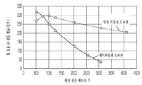
도파관의 길이 및 행에서의 샘플 웰들의 수는 샘플 웰들의 행 사이에 분포된 강도의 균일성에 영향을 미칠 수 있는 추가적인 파라미터들이다. 도 2g 및 도 2h는 행에서의 상이한 수의 샘플 웰들에 대해 균일한 강도를 갖도록 설계된 테이퍼링된 도파관들에 대한 시뮬레이션 결과들을 도시한다. 구체적으로, 도 2g는 도파관에 대한 전력 입력 대 행당 샘플 웰들의 수의 플롯이고, 도 2h는 단위 전력당 센서들의 수 대응하는 행 효율 대 행당 샘플 웰들의 수의 플롯이다. 도 2g에 도시된 바와 같이, 입력 전력은 행에서의 샘플 웰들의 수가 증가함에 따라 증가한다. 도 2h는 행에서의 샘플 웰의 수가 증가함에 따라 효율이 어떻게 감소하는지를 도시한다.The length of the waveguide and the number of sample wells in a row are additional parameters that can affect the uniformity of intensity distributed between the rows of sample wells. 2G and 2H show simulation results for tapered waveguides designed to have uniform intensity for different numbers of sample wells in a row. Specifically, FIG. 2G is a plot of power input for a waveguide versus number of sample wells per row, and FIG. 2H is a plot of number of sample wells per row versus row efficiency corresponding to number of sensors per unit power. As shown in Figure 2G, the input power increases as the number of sample wells in a row increases. 2H shows how the efficiency decreases as the number of sample wells in a row increases.
통합 디바이스에서 테이퍼링된 도파관들을 이용하는 것은 실질적으로 균일한 방식으로 샘플 웰들 사이에 여기 광을 전달하는데 있어서 몇몇 이점들을 제공할 수 있지만, 통합 디바이스가 샘플 웰들의 수를 증가시킴으로써 스케일링됨에 따라 테이퍼링된 도파관들을 이용하는데 있어서 제한들이 있을 수 있다. 도 2g 및 도 2h와 관련하여 논의된 바와 같이, 행에서의 샘플 웰들의 수가 증가함에 따라, 도파관에 대한 더 많은 전력 입력이 필요하고 행 효율이 감소한다. 본 발명자들은 샘플 웰들의 행과 결합하기 위해 다수의 도파관들을 이용하는 것이 테이퍼링된 도파관만을 이용하는 것과 연관된 그러한 제한들을 극복할 수 있다는 것을 인식하고 이해하였다. 다수의 도파관들을 이용하는 것은, 샘플 웰들의 더 긴 행이, 그렇지 않은 경우 단일의 테이퍼링된 도파관을 이용하여 달성되는 것보다 실질적으로 균일한 강도를 갖는 것을 허용할 수 있다. 따라서, 일부 실시예들은 샘플 웰들의 행과 광학적으로 결합하도록 구성된 다수의 도파관들을 갖는 통합 디바이스에 관한 것이다. 일부 실시예들에 따르면, 이러한 구성들은 테이퍼링된 도파관들과 조합하여 이용될 수 있다. 그러한 실시예들에서, 샘플 웰들의 단일 행과 광학적으로 결합하는 다수의 도파관들은 적어도 도파관이 행에서의 샘플 웰들의 서브세트와 결합하는 영역 내에서 테이퍼링될 수 있다. 그러한 구성은 더 많은 수의 샘플 웰들을 갖는 행들이 단일 도파관이 이용된 경우보다 유사한 강도를 수용하는 것을 허용할 수 있다.While using tapered waveguides in an integrated device can provide some advantages in transmitting excitation light between sample wells in a substantially uniform manner, as the integrated device scales by increasing the number of sample wells, tapered waveguides are There may be restrictions on use. 2G and 2H, as the number of sample wells in a row increases, more power input to the waveguide is required and row efficiency decreases. The inventors have recognized and understood that using multiple waveguides to couple with a row of sample wells may overcome such limitations associated with using only tapered waveguides. Using multiple waveguides may allow a longer row of sample wells to have a substantially uniform intensity than would otherwise be achieved using a single tapered waveguide. Accordingly, some embodiments relate to an integrated device having a plurality of waveguides configured to optically couple with a row of sample wells. According to some embodiments, these configurations may be used in combination with tapered waveguides. In such embodiments, multiple waveguides optically coupling a single row of sample wells may be tapered at least in a region where the waveguide couples with a subset of sample wells in the row. Such a configuration may allow rows with a greater number of sample wells to accommodate similar intensities than if a single waveguide was used.
통합 디바이스의 일부 실시예들에서, 제1 도파관은 행에서의 샘플 웰들의 제1 그룹과 광학적으로 결합하도록 위치되고, 제2 도파관은 행에서의 샘플 웰들의 제2 그룹과 광학적으로 결합하도록 위치된다. 샘플 웰들의 제1 및 제2 그룹들 사이에서, 제1 및 제2 도파관들은 샘플 웰들의 행에 대한 포지셔닝(positioning)에서 시프트할 수 있다. 그러한 구성은 샘플 웰들의 제1 및 제2 그룹들 사이에 도파관 "행 시프트"를 갖는 것으로서 간주될 수 있다. 행 시프트의 위치는 샘플 웰들의 행과 제1 도파관의 결합 효율 또는 제1 도파관 내에서 전파하는 전력이 디바이스의 성능이 영향을 받도록 특정 양까지 낮아질 때에 대응할 수 있다. 제2 도파관을 이용하여 행에서의 후속 샘플 웰들에 광을 계속 전달하는 것은 제1 도파관만을 이용하는 것의 이러한 제한들을 제거한다. 추가 도파관들이 동일한 행에서의 샘플 웰들의 추가 그룹들과 광학적으로 결합하도록 포함되고 위치될 수 있다. 이러한 도파관들의 구성은 샘플 웰 어레이에서의 다른 행들에서 구현될 수 있고, 예컨대, 개별 행들에서의 샘플 웰들의 수를 증가시키는 것에 의해, 어레이에서의 샘플 웰들의 수를 증가시키는데 이용될 수 있다.In some embodiments of the integrated device, the first waveguide is positioned to optically couple with a first group of sample wells in the row, and the second waveguide is positioned to optically couple with a second group of sample wells in the row . Between the first and second groups of sample wells, the first and second waveguides may shift in positioning relative to the row of sample wells. Such a configuration may be considered as having a waveguide “row shift” between the first and second groups of sample wells. The location of the row shift may correspond to when the coupling efficiency of the row of sample wells and the first waveguide or power propagating within the first waveguide is lowered by a certain amount such that the performance of the device is affected. Continuing to deliver light to subsequent sample wells in a row using the second waveguide removes these limitations of using only the first waveguide. Additional waveguides may be included and positioned to optically couple with additional groups of sample wells in the same row. This configuration of waveguides may be implemented in different rows in a sample well array and may be used to increase the number of sample wells in the array, eg, by increasing the number of sample wells in individual rows.
도 3a는 샘플 웰들의 개별 행들에 광을 전달하기 위해 다수의 도파관들이 이용되는 행 시프트 도파관 구성을 도시하는 통합 디바이스의 평면도이다. 도파관들에 대한 광 입력의 방향은 화살표로 도시되고 z 방향이다. 도 3a는 샘플 웰들(3-108a, 3-108b 및 3-108c)을 갖는 행 및 샘플 웰들(3-108d, 3-108e 및 3-108f)을 갖는 행을 포함하는 샘플 웰들의 3개의 행들을 도시하고, 여기서 3개의 도파관들은 행들에서의 샘플 웰들의 3개의 상이한 그룹들과 광학적으로 결합하도록(예를 들어, 소멸파에 의해 결합하도록) 위치된다. 예를 들어, 도파관(3-220a)은 샘플 웰(3-108a)과 광학적으로 결합하도록 위치되는 반면, 도파관(3-220b)은 샘플 웰(3-108c)과 광학적으로 결합하도록 위치된다. 다른 예로서, 도파관(3-220d)은 샘플 웰(3-108d)과 광학적으로 결합하도록 위치되는 반면, 도파관(3-220e)은 샘플 웰(3-108f)과 광학적으로 결합하도록 위치된다. 도파관들의 광학 결합은 소멸파 결합을 통해 발생할 수 있는데, 이 경우 도파관을 따라 전파되는 광학 모드의 일부를 수신하도록 샘플 웰에 대해 적절한 거리에서, 도 1a의 도파관(1-220)에 의해 도시된 바와 같이, 도파관이 샘플 웰 아래에 위치된다. 일부 실시예들에 따르면, 도파관(3-220a)은 영역(3-110) 내의 동일한 행에서의 샘플 웰(3-108a) 및 다른 샘플 웰들과 소멸파에 의해 결합하도록 위치될 수 있고, 도파관(3-220b)은 영역(3-114) 내의 동일한 행에서의 샘플 웰(3-108c) 및 다른 샘플 웰들과 소멸파에 의해 결합하도록 위치될 수 있다. 추가의 도파관들은 동일한 행에서의 후속 샘플 웰들에 광을 전달하는데 이용될 수 있다. 예를 들어, 도 3a는 도 3a에 도시된 도면에 존재하지 않는 추가 샘플 웰들과 결합할 수 있는 도파관들(3-220c 및 3-220f)을 도시한다. 특히, 도파관(3-220c)은 샘플 웰(3-108c)과 동일한 행에서의 샘플 웰들과 결합할 수 있고, 도파관(3-220e)은 추가적인 행 시프트 영역이 영역(3-114)을 뒤따른 후에 샘플 웰(3-108f)과 동일한 행에서의 샘플 웰들과 결합할 수 있다.3A is a top view of an integrated device illustrating a row shift waveguide configuration in which multiple waveguides are used to deliver light to individual rows of sample wells. The direction of the light input to the waveguides is shown by the arrow and is the z direction. 3A shows three rows of sample wells comprising a row with sample wells 3-108a, 3-108b and 3-108c and a row with sample wells 3-108d, 3-108e and 3-108f. shown, wherein the three waveguides are positioned to optically couple (eg, by an evanescent wave) with three different groups of sample wells in rows. For example, waveguide 3-220a is positioned to optically couple with sample well 3-108a, while waveguide 3-220b is positioned to optically couple with sample well 3-108c. As another example, waveguide 3-220d is positioned to optically couple with sample well 3-108d, while waveguide 3-220e is positioned to optically couple with sample well 3-108f. Optical coupling of the waveguides may occur via evanescent coupling, as shown by waveguide 1-220 in FIG. Likewise, a waveguide is positioned below the sample well. According to some embodiments, waveguide 3-220a may be positioned to evanescently couple with sample well 3-108a and other sample wells in the same row within region 3-110, waveguide ( 3-220b may be positioned to engage by evanescent wave with sample well 3-108c and other sample wells in the same row within region 3-114. Additional waveguides may be used to deliver light to subsequent sample wells in the same row. For example, FIG. 3A shows waveguides 3-220c and 3-220f that may engage additional sample wells not present in the figure shown in FIG. 3A . In particular, waveguide 3-220c may couple with sample wells in the same row as sample well 3-108c, and waveguide 3-220e is removed after an additional row shift region follows region 3-114. Sample wells in the same row as sample wells 3-108f may be combined.
동일한 행에서의 샘플 웰들은 공통 축을 따라 실질적으로 정렬된 샘플 웰들에 대응할 수 있다. 특정 행에 대해, 영역(3-110)에서의 샘플 웰들의 그룹은 축을 따라 실질적으로 정렬될 수 있다. 도 3a에 도시된 바와 같이, 샘플 웰들(3-108a, 3-108b 및 3-108c)은 축을 따라 (z 방향으로) 정렬되고, 동일한 행에 있는 것으로 간주된다. 도파관들은 축에 대해 위치될 수 있다. 일부 실시예들에서, 샘플 웰들의 그룹과 결합하도록 구성된 도파관의 일부는 축에 실질적으로 평행할 수 있고, 다수의 도파관들은 샘플 웰들의 상이한 그룹들과 광학적으로 결합할 수 있고, 샘플 웰들의 행을 따르는 상이한 부분들에서 축에 실질적으로 평행할 수 있다. 도 3a에 도시된 바와 같이, 도파관(3-220a)은 영역(3-110) 내의 샘플 웰들(3-108a, 3-108b 및 3-108c)을 따른 축에 실질적으로 평행하고, 도파관(3-220b)은 영역(3-114) 내의 축에 실질적으로 평행하다.Sample wells in the same row may correspond to sample wells substantially aligned along a common axis. For a particular row, the group of sample wells in region 3 - 110 may be substantially aligned along an axis. As shown in FIG. 3A , sample wells 3-108a , 3-108b and 3-108c are aligned along the axis (in the z direction) and are considered to be in the same row. The waveguides may be positioned relative to the axis. In some embodiments, a portion of a waveguide configured to couple with a group of sample wells may be substantially parallel to an axis, and a plurality of waveguides may optically couple different groups of sample wells, forming a row of sample wells. It may be substantially parallel to the axis at different portions along it. As shown in FIG. 3A , waveguide 3-220a is substantially parallel to an axis along sample wells 3-108a , 3-108b and 3-108c in region 3-110 , and waveguide 3 - 220b) is substantially parallel to the axis in region 3 - 114 .
도파관들 사이의 간격은 도파관들이 사실상 광학적으로 서로 분리되도록 될 수 있다. 일부 실시예들에서, 하나의 도파관은 2개의 도파관들 사이에 소멸파 결합이 없거나 거의 없도록 다른 도파관으로부터 분리될 수 있다. 일부 실시예들에서, 2개의 도파관들 사이의 측방향 거리는 도파관들이 갖도록 구성되는 광학 모드 크기에 의존할 수 있다.The spacing between the waveguides may be such that the waveguides are substantially optically separated from each other. In some embodiments, one waveguide may be separated from the other such that there is little or no evanescent coupling between the two waveguides. In some embodiments, the lateral distance between two waveguides may depend on the optical mode size the waveguides are configured to have.
도 3a에 도시된 도파관 구성은 영역들(3-110, 3-112 및 3-114)을 갖는다. 영역(3-110)은 도파관(3-220a)과 같은 제1 도파관이 샘플 웰(3-108a)과 같은 행에서의 샘플 웰들의 제1 그룹과 광학적으로 결합하여, 광을 샘플 웰들의 제1 그룹에 전달하는 곳이다. 영역(3-114)은 도파관(3-220b)과 같은 제2 도파관이 샘플 웰(3-108c)과 같은 행에서의 샘플 웰들의 제2 그룹과 광학적으로 결합하여, 광을 샘플 웰들의 제2 그룹에 전달하는 곳이다. 영역(3-112)은 제1 및 제2 도파관들 사이의 행 시프트가 발생하는 곳에 대응한다. 도 3a에 도시된 바와 같이, 행 시프트 구성은 제1 도파관이 행에서의 샘플 웰들과 광학적으로 결합하도록 위치되지 않는 반면, 제2 도파관이 행에서의 샘플 웰들과 광학적으로 결합하도록 위치되도록, 도파관들을 만곡시키는 것을 포함한다. 행 시프트 구성은 제1 도파관과 영역(3-110)에서의 샘플 웰 사이의 거리가 제1 도파관과 영역(3-112)에서의 샘플 웰 사이의 거리보다 작아지게 한다. 행 시프트 구성은 또한, 제2 도파관과 영역(3-114)에서의 샘플 웰 사이의 거리가 제2 도파관과 영역(3-112)에서의 샘플 웰 사이의 거리보다 작아지게 한다. 예를 들어, 도파관들(3-220a 및 3-220d)은 영역(3-112)에서 샘플 웰들의 그들 각각의 행들로부터 (x 방향을 따라) 오프셋되도록 만곡되고, 오프셋은 도파관들을 통한 광 전파의 방향을 따라 증가한다. 추가적으로, 도파관들(3-220b 및 3-220e)은 영역(3-112)에서 만곡되고 샘플 웰들의 그들 각각의 행들로부터 (x 방향을 따라) 오프셋되지만, 오프셋은 도파관들을 통한 광 전파의 방향을 따라 감소하여 도파관들(3-220b 및 3-220e)을 샘플 웰 행들에 더 근접하게 위치시킨다. 영역(3-112)에서의 행 시프팅 프로파일은 임의의 적절한 프로파일 및/또는 길이를 가질 수 있다. 도 3a에 도시된 도파관들은 영역(3-112)에서 유사한 행 시프트 프로파일을 갖지만, 일부 실시예들은 영역(3-112) 내에서 상이한 프로파일들을 갖는 동일한 행에 결합하는 도파관들을 포함할 수 있다는 것을 이해해야 한다.The waveguide configuration shown in FIG. 3A has regions 3-110, 3-112 and 3-114. Region 3-110 is such that a first waveguide, such as waveguide 3-220a, optically couples with a first group of sample wells in the same row as sample well 3-108a, thereby directing light to a first of the sample wells. This is where you pass it on to the group. Region 3-114 is such that a second waveguide, such as waveguide 3-220b, optically couples with a second group of sample wells in the same row as sample well 3-108c, thereby directing light to a second of the sample wells. This is where you pass it on to the group. Regions 3-112 correspond to where a row shift between the first and second waveguides occurs. 3A , the row shift configuration moves the waveguides such that the first waveguide is not positioned to optically couple with the sample wells in the row, while the second waveguide is positioned to optically couple with the sample wells in the row. including curvature. The row shift configuration causes the distance between the first waveguide and the sample well in region 3 - 110 to be less than the distance between the first waveguide and the sample well in region 3 - 112 . The row shift configuration also causes the distance between the second waveguide and the sample well in region 3 - 114 to be less than the distance between the second waveguide and the sample well in region 3 - 112 . For example, waveguides 3-220a and 3-220d are curved such that they are offset (along the x-direction) from their respective rows of sample wells in region 3-112, where the offset is of light propagation through the waveguides. increases along the direction. Additionally, waveguides 3-220b and 3-220e are curved in region 3-112 and are offset (along the x direction) from their respective rows of sample wells, but the offset determines the direction of light propagation through the waveguides. decreases to place waveguides 3-220b and 3-220e closer to the sample well rows. The row shifting profile in regions 3 - 112 may have any suitable profile and/or length. Although the waveguides shown in FIG. 3A have a similar row shift profile in region 3 - 112 , it should be understood that some embodiments may include waveguides coupling in the same row with different profiles within region 3 - 112 . do.
일부 실시예들에서, 행에서의 샘플 웰들과 광학적으로 결합하도록 구성된 도파관의 영역은, 도파관이 그 영역에서 결합하는 샘플 웰들의 그룹에 대해 실질적으로 균일한 강도를 달성하기 위해, 예컨대, 본 명세서에 설명된 기술들을 이용하는 것에 의해 테이퍼링될 수 있다. 도 3a에 도시된 바와 같이, 도파관(3-220a)은 영역(3-110) 내에서 테이퍼링되고, 도파관(3-220b)은 영역(3-114) 내에서 테이퍼링된다.In some embodiments, a region of a waveguide configured to optically couple with sample wells in a row is defined herein, e.g., in order to achieve a substantially uniform intensity over a group of sample wells to which the waveguide couples in that region. It can be tapered by using the described techniques. As shown in FIG. 3A , waveguide 3-220a is tapered in region 3-110, and waveguide 3-220b is tapered in region 3-114.
통합 디바이스는 개별 도파관들 내로 입력 전력을 제공하기 위해 하나 이상의 광학 컴포넌트(예를 들어, 도 1a에 도시된 라우팅 영역(1-202) 내에 위치된 광학 스플리터들)를 포함할 수 있다. 일부 실시예들에서, 입력 전력은 모든 도파관들에 걸쳐 실질적으로 동일할 수 있다. 본 발명자들은 행에서의 샘플 웰들의 그룹과 광학적으로 결합되지 않은 도파관들이, 광이 이 영역을 통해 전파될 때 일부 광학 손실을 겪을 수 있다는 것을 인식하고 이해하였다. 따라서, 일부 실시예들은 도파관들이 각각의 샘플 웰들에 광학적으로 결합하는 영역들에서 도파관들의 하나 이상의 특성을 변화시킴으로써 그러한 광학 손실을 감소시키는 구성을 가질 수 있다. 예를 들어, 영역(3-110)에서의 도파관(3-220b)의 부분은 광학 손실을 감소시키는 구성을 가질 수 있지만, 도파관(3-220a)이 영역(3-110)에서의 샘플 웰들에 광학적으로 결합할 때보다 도파관(3-220b)이 영역(3-114)에서의 샘플 웰들에 광학적으로 결합할 때 여전히 더 낮은 양의 전력을 전달할 수 있다. 따라서, 샘플 웰들의 행에 광을 전달하는 도파관들의 테이퍼링은 도파관들이 샘플 웰들에 결합하기 위해 이용될 때 광학 전력에서의 이러한 변화를 고려하기 위해 상이할 수 있다. 일부 실시예들에서, 영역(3-110)에서의 제1 도파관의 테이퍼링된 부분의 길이는 영역(3-114)에서의 제2 도파관의 테이퍼링된 부분의 길이와 상이할 수 있다. 테이퍼링된 부분의 길이는 특정 도파관이 도파관의 해당 테이퍼링된 영역 내로 광을 전달하기 위해 이용되는 샘플 웰들의 수에 대응할 수 있다. 일부 실시예들에서, 영역(3-114)에서의 제2 도파관의 테이퍼링된 부분의 길이는 영역(3-110)에서의 제1 도파관의 테이퍼링된 부분의 길이보다 짧을 수 있다. 그러한 구성은 영역(3-110)에서의 제1 도파관보다 영역(3-114)에서 더 낮은 광학 전력을 갖는 제2 도파관을 고려할 수 있다. 예를 들어, 도 3a는 도파관(3-220a)의 테이퍼링된 부분의 길이에 대응할 수 있는 6개의 샘플 웰들과 결합하는 영역(3-110)에서의 도파관(3-220a)의 테이퍼링된 부분을 도시하지만, 영역(3-114)에서의 도파관(3-220b)의 테이퍼링된 부분은 5개의 샘플 웰들과 결합하는 것으로 도시된다. 제1 및 제2 도파관들의 테이퍼링된 부분들은 도 3a에 도시된 것보다 많거나 적은 샘플 웰들과 결합될 수 있다는 것을 이해해야 한다.The integrated device may include one or more optical components (eg, optical splitters located within routing area 1-202 shown in FIG. 1A ) to provide input power into individual waveguides. In some embodiments, the input power may be substantially the same across all waveguides. The inventors have recognized and understood that waveguides that are not optically coupled with a group of sample wells in a row may experience some optical loss as light propagates through this region. Accordingly, some embodiments may be configured to reduce such optical loss by changing one or more properties of the waveguides in the regions where they optically couple to respective sample wells. For example, the portion of waveguide 3-220b in region 3-110 may have a configuration that reduces optical loss, while waveguide 3-220a is connected to the sample wells in region 3-110. Waveguide 3-220b may still deliver a lower amount of power when optically coupling to the sample wells in region 3-114 than when optically coupling. Thus, the tapering of the waveguides that transmit light to a row of sample wells may be different to account for this change in optical power when the waveguides are used to couple to the sample wells. In some embodiments, the length of the tapered portion of the first waveguide in region 3 - 110 may be different from the length of the tapered portion of the second waveguide in region 3 - 114 . The length of the tapered portion may correspond to the number of sample wells in which a particular waveguide is used to deliver light into the corresponding tapered region of the waveguide. In some embodiments, the length of the tapered portion of the second waveguide in region 3 - 114 may be shorter than the length of the tapered portion of the first waveguide in region 3 - 110 . Such a configuration may allow for a second waveguide having a lower optical power in region 3 - 114 than the first waveguide in region 3 - 110 . For example, FIG. 3A shows a tapered portion of waveguide 3-220a in region 3-110 engaging six sample wells that may correspond to the length of the tapered portion of waveguide 3-220a. However, the tapered portion of waveguide 3-220b in region 3-114 is shown engaging five sample wells. It should be understood that the tapered portions of the first and second waveguides may engage more or fewer sample wells than shown in FIG. 3A .
일부 실시예들에서, 도파관들의 행 시프팅이 발생하는 곳에 위치한 행 내의 샘플 웰들은, 행에서의 다른 샘플 웰들과 비교하여, 도파관과 광학적으로 결합하지 않거나 도파관과의 더 낮은 양의 광학적 결합을 가질 수 있다. 따라서, 샘플 웰 어레이의 행 시프팅 영역 내에 위치한 샘플 웰들은 더 낮은 양의 광학 전력을 수신할 수 있다. 샘플의 분석을 수행하는데 있어서 통합 디바이스의 동작 동안, 이들 샘플 웰들은 이들 샘플 웰들에 의해 얻어진 결과들의 품질이 원하는 양의 광(예를 들어, 특정한 강도)으로 샘플을 조명하기에 불충분한 능력에 의해 영향을 받을 수 있기 때문에 분석의 결과들로부터 배제될 수 있다. 도 3a에 도시된 바와 같이, 영역(3-112)에서의 샘플 웰들의 그룹은 영역(3-110)에서의 샘플 웰 또는 동일한 행의 3-114에서의 샘플 웰보다 적은 광학 전력을 수신할 수 있다. 이것은 영역(3-112)에 위치된 샘플 웰이 행에 대한 대응하는 제1 또는 제2 도파관과 광학적으로 결합하지 않거나 원하는 효율로 광학적으로 결합하지 않을 수 있기 때문이다. 예를 들어, 영역(3-112)은 샘플 웰(3-108b)을 포함하고, 이는 샘플 웰들(3-108a 및 3-108c)과 같은 영역들(3-110 및 3-114)에서의 샘플 웰들과 비교하여 더 낮은 양의 광학 전력을 수신할 수 있는데, 그 이유는 샘플 웰(3-108b)이 양쪽 도파관들(3-220a 및 3-220b)로부터 오프셋되기 때문이다. 유사하게, 영역(3-112)은 샘플 웰들(3-108d 및 3-108f)에 비해 더 낮은 양의 광학 전력을 수신할 수 있는 샘플 웰(3-108e)을 포함한다. 따라서, 통합 디바이스의 동작 동안 샘플 웰들(3-108b 및 3-108e)을 이용하여 획득된 데이터는 전체 결과들로부터 배제될 수 있다.In some embodiments, sample wells in a row located where row shifting of the waveguides occurs do not optically couple with the waveguide or have a lower amount of optical coupling with the waveguide compared to other sample wells in the row can Thus, sample wells located within the row shifting region of the sample well array may receive a lower amount of optical power. During operation of the integrated device in performing an analysis of a sample, these sample wells may be affected by an insufficient ability to illuminate the sample with a desired amount of light (eg, a particular intensity) in which the quality of results obtained by these sample wells is insufficient. It can be excluded from the results of the analysis because it may be affected. As shown in FIG. 3A , a group of sample wells in region 3-112 may receive less optical power than a sample well in region 3-110 or a sample well in 3-114 in the same row. have. This is because the sample wells located in regions 3 - 112 may not optically couple or with a desired efficiency with the corresponding first or second waveguide for the row. For example, region 3-112 includes sample well 3-108b, which includes sample in regions 3-110 and 3-114, such as sample wells 3-108a and 3-108c. It may receive a lower amount of optical power compared to the wells because sample well 3-108b is offset from both waveguides 3-220a and 3-220b. Similarly, region 3-112 includes sample well 3-108e that may receive a lower amount of optical power compared to sample wells 3-108d and 3-108f. Thus, data obtained using sample wells 3-108b and 3-108e during operation of the integrated device may be excluded from the overall results.
도 3a에 도시된 바와 같은 행 시프트 구성을 갖는 도파관 어레이는 본 명세서에 설명된 하나 이상의 다른 컴포넌트와 조합하여 통합 디바이스에서 구현될 수 있다. 일부 실시예들에서, 행 시프트 도파관 구성을 갖는 통합 디바이스는 통합 디바이스의 표면으로부터 광을 수신하여, 도파관들과 광학적으로 결합하도록 구성된 격자 커플러를 포함할 수 있다. 도 3a의 맥락에서, 격자 커플러는 도 3a에 도시된 화살표의 방향으로 광을 제공하기 위해 (네거티브 z 방향으로) 좌측에 위치될 수 있다. 일부 실시예들에서, 행 시프트 도파관 구성을 갖는 통합 디바이스는 하나 이상의 광검출기와 동일한 픽셀에서의 샘플 웰로부터 방출된 광을 수신하도록 구성된 하나 이상의 광검출기를 포함할 수 있다. 예를 들어, 샘플 웰(3-108a)을 갖는 픽셀은 샘플 웰(3-108a)로부터 방출된 광을 수신하도록 위치되고 구성된 하나 이상의 광검출기를 포함할 수 있다. 픽셀은 도 1a의 픽셀(1-112)에 의해 도시된 바와 같은 단면 구성을 가질 수 있다.A waveguide array having a row shift configuration as shown in FIG. 3A may be implemented in an integrated device in combination with one or more other components described herein. In some embodiments, an integrated device having a row shift waveguide configuration may include a grating coupler configured to receive light from a surface of the integrated device and optically couple with the waveguides. In the context of FIG. 3A , the grating coupler may be positioned to the left (in the negative z direction) to provide light in the direction of the arrow shown in FIG. 3A . In some embodiments, an integrated device having a row shift waveguide configuration may include one or more photodetectors and one or more photodetectors configured to receive light emitted from a sample well in the same pixel. For example, a pixel having sample well 3 - 108a may include one or more photodetectors positioned and configured to receive light emitted from sample well 3 -108a. The pixel may have a cross-sectional configuration as shown by pixels 1-112 in FIG. 1A.
본 발명자들은 광학 전력의 소스로서 작용하고 행에서의 샘플 웰들과 광학적으로 결합하도록 위치되는 하나 이상의 다른 도파관에 광학적으로 결합하는 샘플 웰들의 행 마다 도파관을 갖는 어레이 도파관 구성들이 특정 이점들을 제공할 수 있다는 것을 인식하고 이해하였다. 광학 전력의 소스로서 작용하는 도파관은 "전력 도파관"으로서 고려될 수 있다. 그러한 구성들의 하나의 이점은 어레이 도파관들의 전체 풋프린트(footprint)가 감소될 수 있다는 것이며, 이는 샘플 웰들의 행들 사이의 거리가 작고 샘플 웰들의 행들 사이에 위치된 다수의 도파관들을 수용하지 않을 수 있는 통합 디바이스들을 구성하는데 있어서 이점들을 제공할 수 있다. 따라서, 통합 디바이스의 일부 실시예들은 샘플 웰 어레이의 개별 행들과 연관된 전력 도파관들 및 대응하는 행에서의 하나 이상의 전력 도파관 및 샘플 웰과 광학적으로 결합하는 하나 이상의 도파관을 포함할 수 있다. 일부 실시예들에서, 하나 이상의 다른 도파관은 광학 스플리터(예를 들어, 방향성 커플러)를 통해 전력 도파관과 광학적으로 결합할 수 있다. 일부 실시예들에서, 샘플 웰들의 행은 행과 연관된 전력 도파관과 광학적으로 결합하고, 행에서의 샘플 웰들과 광학적으로 결합하는 연속 커플러로서 작용하는 도파관을 갖는다.The inventors have discovered that array waveguide configurations having a waveguide per row of sample wells that act as a source of optical power and optically couple to one or more other waveguides positioned to optically couple with the sample wells in the row can provide certain advantages. recognized and understood A waveguide that acts as a source of optical power may be considered a “power waveguide”. One advantage of such configurations is that the overall footprint of the array waveguides can be reduced, which means that the distance between rows of sample wells is small and may not accommodate multiple waveguides positioned between rows of sample wells. It can provide advantages in constructing integrated devices. Accordingly, some embodiments of an integrated device may include power waveguides associated with individual rows of a sample well array and one or more power waveguides in a corresponding row and one or more waveguides optically coupled with the sample well. In some embodiments, one or more other waveguides may optically couple with the power waveguide via an optical splitter (eg, a directional coupler). In some embodiments, a row of sample wells has a waveguide that optically couples with a power waveguide associated with the row and acts as a continuous coupler that optically couples with the sample wells in the row.
도 3b는 샘플 웰들의 행에 대해, 행에서의 샘플 웰들의 상이한 그룹들과 광학적으로 결합하도록 위치된 전력 도파관 및 다수의 도파관들을 포함하는 어레이 도파관 구성을 갖는 통합 디바이스의 평면도이다. 샘플 웰들(3-208a 및 3-208b)은 동일한 행에 있고, 도파관(3-230a)은 그 행에 대한 전력 도파관으로서 작용한다. 유사하게, 샘플 웰들(3-208c 및 3-208d)은 상이한 행에 있고, 도파관(3-230b)은 그 행에 대한 전력 도파관으로서 작용한다. 전력 도파관들을 따른 광 전파의 방향은 도 3b의 화살표에 의해 도시된다. 전력 도파관을 따라, 개별 도파관들은 전력 도파관과 결합되고, 행에서의 샘플 웰들의 그룹과 광학적으로 결합되도록 위치된다. 도 3b에서, 도파관들(3-240a 및 3-240b)은 전력 도파관(3-230a)과 광학적으로 결합하고, 샘플 웰들(3-208a 및 3-208b)을 갖는 행에서의 샘플 웰들에 광을 전달하도록 구성된다. 일부 실시예들에서, 도파관들(3-240a 및 3-240b)은, 예컨대 본 명세서에 설명된 테이퍼링된 도파관들을 이용함으로써, 이들 도파관들과 광학적으로 결합하는 샘플 웰들에 대해 실질적으로 균일한 강도를 제공하도록 테이퍼링된다. 도 3b에 도시된 바와 같이, 샘플 웰(3-208a)은 샘플 웰(3-208b)이 광학적으로 결합하는 도파관(3-240a)의 영역보다 큰 폭을 갖는 도파관(3-240a)의 영역과 광학적으로 결합하도록 구성된다. 유사하게, 샘플 웰(3-208f)은 샘플 웰(3-208g)이 광학적으로 결합하는 도파관(3-240b)의 영역보다 큰 폭을 갖는 도파관(3-240b)의 영역과 광학적으로 결합하도록 구성된다. 또한, 샘플 웰들(3-208a 및 3-208b)과 상이한 행에 있는 샘플 웰들(3-208c 및 3-208d)은 상이한 폭들을 갖는 도파관(3-240c)의 상이한 영역들과 광학적으로 상부 결합하도록 구성된다. 특히, 샘플 웰(3-208c)은 샘플 웰(3-208d)이 광학적으로 결합하는 도파관(3-240c)의 영역보다 큰 폭을 갖는 도파관(3-240c)의 영역과 광학적으로 결합하도록 구성된다.3B is a top view of an integrated device having an array waveguide configuration comprising multiple waveguides and a power waveguide positioned to optically couple with different groups of sample wells in the row, for a row of sample wells. Sample wells 3-208a and 3-208b are in the same row, and waveguide 3-230a acts as a power waveguide for that row. Similarly, sample wells 3-208c and 3-208d are in different rows, and waveguide 3-230b acts as a power waveguide for that row. The direction of light propagation along the power waveguides is shown by the arrow in FIG. 3B . Along the power waveguide, individual waveguides are coupled to the power waveguide and positioned to optically couple with a group of sample wells in a row. In FIG. 3B , waveguides 3-240a and 3-240b optically couple with power waveguide 3-230a and provide light to the sample wells in a row with sample wells 3-208a and 3-208b. configured to deliver. In some embodiments, waveguides 3-240a and 3-240b provide substantially uniform intensity for sample wells optically coupling these waveguides, such as by using the tapered waveguides described herein. tapered to provide As shown in FIG. 3B , sample well 3-208a includes an area of waveguide 3-240a having a width greater than the area of waveguide 3-240a to which sample well 3-208b optically couples; configured to be optically coupled. Similarly, sample well 3-208f is configured to optically couple with a region of waveguide 3-240b having a width greater than the region of waveguide 3-240b to which sample well 3-208g optically couples. do. Also, sample wells 3-208c and 3-208d in a different row than sample wells 3-208a and 3-208b are configured to optically top-couple with different regions of waveguide 3-240c having different widths. is composed In particular, sample well 3-208c is configured to optically couple with a region of waveguide 3-240c having a width greater than the region of waveguide 3-240c to which sample well 3-208d optically couples. .
전력 도파관들(3-230a 및 3-230b)은, 예컨대, 도파관의 길이를 따라 실질적으로 균일한 폭을 갖는 것에 의해, 광이 도파관을 따라 전파할 때 광학 손실을 감소시키는 구성을 가질 수 있다. 도 3b에 도시된 바와 같이, 도파관들(3-240a 및 3-240b)은 각각 전력 스플리터들(3-250a 및 3-250b)을 통해 전력 도파관(3-230a)과 광학적으로 결합할 수 있다. 또한, 도파관들(3-240c 및 3-240d)은 하나 이상의 전력 스플리터를 통해 전력 도파관(3-230b)과 광학적으로 결합할 수 있다. 적절한 전력 스플리터들의 예들은 방향성 커플러들, 다중모드 간섭 스플리터들, 또는 임의의 다른 적절한 전력 분할 광학 컴포넌트를 포함한다. 방향성 커플러들이 전력 스플리터들로서 이용되는 실시예들에서, 방향성 커플러의 구성은 샘플 웰들의 그룹과 광학적으로 결합하는 도파관 내에 입력되는 광학 전력의 원하는 상대량을 달성하기 위해 특정 전력 분할비(power splitting ratio)를 위해 구성될 수 있다.Power waveguides 3-230a and 3-230b may be configured to reduce optical loss as light propagates along the waveguide, eg, by having a substantially uniform width along the length of the waveguide. As shown in FIG. 3B , waveguides 3-240a and 3-240b may optically couple with power waveguide 3-230a via power splitters 3-250a and 3-250b, respectively. Further, waveguides 3-240c and 3-240d may optically couple with power waveguide 3-230b via one or more power splitters. Examples of suitable power splitters include directional couplers, multimode interference splitters, or any other suitable power splitting optical component. In embodiments where directional couplers are used as power splitters, the configuration of the directional coupler may be configured to achieve a specific power splitting ratio to achieve a desired relative amount of optical power input into a waveguide that optically couples with a group of sample wells. can be configured for
일부 실시예들에서, 전력 도파관과 광학적으로 결합하는 개별 전력 스플리터들은 유사한 분할비를 가질 수 있다. 도 3b를 참조하면, 전력 스플리터(3-250a) 및 전력 스플리터(3-250b)는 전력 도파관(3-230a)과 동일한 분할비를 가질 수 있다. 그러한 경우들에서, 도파관(3-240b)은, 전력 도파관(3-230a)이 전력 스플리터(3-250b) 전에 전력 스플리터(3-250a)와 결합하기 때문에, 광이 3-230a를 따라 전파할 때 도파관(3-240a)보다 더 적은 광학 전력을 수신하도록 구성된다. 그러한 실시예들에서, 도파관들(3-240a 및 3-240b)은, 도파관들(3-240a 및 3-240b)과 광학적으로 결합하도록 구성된 샘플 웰들이 실질적으로 유사한 강도들을 수신하도록 입력 전력에서의 차이들을 수용하기 위해 상이한 테이퍼링된 형상들을 가질 수 있고, 따라서 도파관들(3-240a 및 3-240b)의 상이한 테이퍼링된 형상들은 전력 스플리터들(3-250a 및 3-250b)을 통해 전력 스플리터(3-230a)로부터 도파관들(3-240a 및 3-240b)에 의해 수신된 광학 전력의 차이들을 고려할 수 있다. 예를 들어, 도파관(3-240b)은 전력 도파관(3-230a)으로부터 더 낮은 입력 전력을 수신하는 것을 고려하기 위해 도파관(3-240a)보다 더 짧은 테이퍼 길이를 가질 수 있다.In some embodiments, individual power splitters that optically couple with the power waveguide may have a similar split ratio. Referring to FIG. 3B , the power splitter 3-250a and the power splitter 3-250b may have the same split ratio as that of the power waveguide 3-230a. In such cases, waveguide 3-240b prevents light from propagating along 3-230a because power waveguide 3-230a couples with power splitter 3-250a before power splitter 3-250b. when configured to receive less optical power than the waveguide 3-240a. In such embodiments, waveguides 3-240a and 3-240b are configured to provide substantially similar intensities at input power such that sample wells configured to optically couple with waveguides 3-240a and 3-240b receive substantially similar intensities. It may have different tapered shapes to accommodate differences, so that the different tapered shapes of waveguides 3-240a and 3-240b are passed through power splitters 3-250a and 3-250b to
일부 실시예들에서, 전력 도파관과 광학적으로 결합하는 개별 전력 스플리터들은 샘플 웰들과 광학적으로 결합하는 도파관들이 실질적으로 유사한 입력 전력을 수신하도록 상이한 분할비들을 가질 수 있다. 도 3b를 참조하면, 전력 스플리터(3-250a) 및 전력 스플리터(3-250b)는 유사한 양의 광학 전력이 도파관들(3-240a 및 3-240b)에 결합되도록 전력 도파관(3-230a)과 상이한 분할비들을 가질 수 있다. 그러한 실시예들에서, 도파관들(3-230a 및 3-230b)은 도파관들(3-230a 및 3-230b)과 광학적으로 결합하는 샘플 웰들이 실질적으로 유사한 강도들을 수신하는 것을 허용하기 위해 유사한 테이퍼링된 형상을 가질 수 있다.In some embodiments, the individual power splitters optically coupling the power waveguide may have different split ratios such that the waveguides optically coupling the sample wells receive substantially similar input power. 3B, power splitter 3-250a and power splitter 3-250b are coupled with power waveguide 3-230a such that a similar amount of optical power is coupled to waveguides 3-240a and 3-240b. It can have different split ratios. In such embodiments, waveguides 3-230a and 3-230b have a similar tapering to allow sample wells optically coupling waveguides 3-230a and 3-230b to receive substantially similar intensities. may have a given shape.
일부 실시예들은 행 내의 샘플 웰들에 광학적으로 결합하는 개별 도파관들 사이의 전이 영역을 포함할 수 있다. 전이 영역 내에 위치한 샘플 웰들은 도파관들 중 하나와 광학적으로 결합하거나, 전이 영역 외부의 행에서의 다른 샘플 웰들과 유사한 양의 광학 전력을 수신하도록 위치되지 않을 수 있다. 도 3b에 도시된 바와 같이, 샘플 웰(3-208e)은 도파관들(3-240a 및 3-240b) 사이의 전이 영역 내에 위치한 샘플 웰의 예이다. 샘플 웰(3-208e)은 샘플 웰들(3-208a 및 3-208b)보다 낮은 양의 광학 전력을 수신할 수 있다. 그러한 경우들에서, 샘플 웰(3-208e)을 이용하여 획득된 임의의 데이터는 분석으로부터 배제될 수 있는데, 그 이유는 그것이 샘플 웰(3-208a 및 3-208b)과 같은 다른 샘플 웰들에 비해 더 적은 양의 여기 광을 수신하기 때문이다.Some embodiments may include transition regions between individual waveguides that optically couple to sample wells in a row. Sample wells located within the transition region may not be positioned to optically couple with one of the waveguides or to receive a similar amount of optical power as other sample wells in a row outside the transition region. As shown in FIG. 3B , sample well 3-208e is an example of a sample well located within the transition region between waveguides 3-240a and 3-240b. Sample well 3-208e may receive a lower amount of optical power than sample wells 3-208a and 3-208b. In such cases, any data obtained using sample well 3-208e may be excluded from analysis because it is compared to other sample wells, such as sample wells 3-208a and 3-208b. This is because it receives a smaller amount of excitation light.
일부 실시예들에서, 통합 디바이스는 샘플 웰들의 하나보다 많은 행에 광학 전력을 전달하도록 구성된 전력 도파관을 포함할 수 있다. 도 3c는 전력 도파관(3-330a)에 인접한 샘플 웰들의 2개의 행들에 광을 전달하도록 구성된 전력 도파관(3-330a)을 갖는 통합 디바이스의 평면도이다. 특히, 전력 도파관(3-330a)은 샘플 웰들(3-308a 및 3-308b)을 포함하는 샘플 웰들의 행 및 샘플 웰들(3-308c 및 3-308d)을 포함하는 샘플 웰들의 행과 광학적으로 결합하도록 구성된다. 도 3c에 도시된 구성에서와 같이, 이들 2개의 행들에서의 샘플 웰들은 도파관들과 전력 스플리터들의 조합을 통해 전력 도파관(3-330a)에 광학적으로 결합할 수 있다. 도파관(3-340a)은 샘플 웰들(3-308a 및 3-308b)과 광학적으로 결합하도록 위치되고, 전력 스플리터를 통해 전력 도파관(3-330a)에 광학적으로 결합할 수 있다. 도파관(3-340b)은 샘플 웰들(3-308c 및 3-308d)과 광학적으로 결합하도록 위치되고, 전력 스플리터를 통해 전력 도파관(3-330a)에 광학적으로 결합할 수 있다. 도 3c와 관련하여 설명된 도파관들 및 전력 스플리터들은 도파관들(3-340a 및 3-340b)에 이용될 수 있고, 전력 스플리터들은 이러한 도파관들을 전력 도파관(3-330a)에 결합하는데 이용될 수 있다. 유사하게, 전력 도파관(3-330b)은 샘플 웰들(3-308e 및 3-308f)을 포함하는 샘플 웰들의 행에, 그리고 3-308g 및 3-308h를 포함하는 샘플 웰들의 행에 광을 전달하도록 구성된다. 특히, 도파관(3-340c)은 전력 도파관(3-330b) 및 샘플 웰들(3-308e 및 3-308f)과 광학적으로 결합하도록 위치되고, 도파관(3-340d)은 전력 도파관(3-330b) 및 샘플 웰들(3-308g 및 3-308h)과 광학적으로 결합하도록 위치된다.In some embodiments, the integrated device can include a power waveguide configured to deliver optical power to more than one row of sample wells. 3C is a top view of an integrated device having a power waveguide 3-330a configured to deliver light to two rows of sample wells adjacent to the power waveguide 3-330a. In particular, power waveguide 3-330a is optically coupled with a row of sample wells comprising sample wells 3-308a and 3-308b and a row of sample wells comprising sample wells 3-308c and 3-308d. configured to combine. As in the configuration shown in FIG. 3C , the sample wells in these two rows may optically couple to power waveguide 3-330a via a combination of waveguides and power splitters. Waveguide 3-340a may be positioned to optically couple with sample wells 3-308a and 3-308b and optically couple to power waveguide 3-330a via a power splitter. Waveguide 3-340b may be positioned to optically couple with sample wells 3-308c and 3-308d and optically couple to power waveguide 3-330a via a power splitter. The waveguides and power splitters described in connection with FIG. 3C may be used in waveguides 3-340a and 3-340b, and power splitters may be used to couple these waveguides to power waveguide 3-330a. . Similarly, power waveguide 3-330b delivers light to a row of sample wells comprising sample wells 3-308e and 3-308f, and to a row of sample wells comprising 3-308g and 3-308h. configured to do In particular, waveguide 3-340c is positioned to optically couple with power waveguide 3-330b and sample wells 3-308e and 3-308f, and waveguide 3-340d includes power waveguide 3-330b. and optically coupled with sample wells 3-308g and 3-308h.
일부 실시예들에서, 행에서의 샘플 웰들과 광학적으로 결합하도록 위치된 도파관은, 예컨대, 전력 도파관의 단부를 통해 전력 도파관에 접속될 수 있다. 예를 들어, 샘플 웰들의 행과 광학적으로 결합하도록 구성된 일련의 도파관들이 있고, 광이 전력 도파관을 통해 일련의 도파관들에 광학적으로 결합되는 도파관 구성들에서, 전력 도파관의 광 입력 단부로부터 더 멀리 있는 일련의 도파관은, 예컨대, 광학 접속을 통해 전력 도파관에 직접 접속될 수 있다. 그러한 구성에서, 전력 도파관을 따라 전파하는 광은 광학 접속을 통해 전파함으로써 도파관에 전달될 수 있다. 도 3d는 전력 도파관(3-430)을 갖는 도파관 구성의 평면도이고, 여기서 화살표는 전력 도파관(3-430)에 대한 광 입력의 방향을 도시한다. 도파관들(3-440a, 3-440b, 3-440c 및 3-440d)은 샘플 웰들(3-408a, 3-408b, 3-408c 및 3-408d)을 갖는 샘플 웰들의 행과 광학적으로 결합하도록 구성된다. 도파관들(3-440a, 3-440b 및 3-440c)은 각각 전력 스플리터들(3-450a, 3-450b 및 3-450c)을 통해 전력 도파관(3-430)과 광학적으로 결합한다. 도파관(3-440d)은 광학 접속(3-460)을 통해 전력 도파관과 접속된다. 광학 접속(3-460)은 전력 도파관(3-430)으로부터 출력된 광을 도파관(3-440d)으로 지향시키기 위한 임의의 적절한 크기 및 형상을 가질 수 있다.In some embodiments, a waveguide positioned to optically couple with sample wells in a row may be connected to the power waveguide, eg, through an end of the power waveguide. For example, in waveguide configurations in which there is a series of waveguides configured to optically couple with a row of sample wells, and wherein light is optically coupled to the series of waveguides via the power waveguide, further away from the light input end of the power waveguide The series of waveguides may be directly connected to the power waveguides, for example, via optical connections. In such a configuration, light propagating along the power waveguide may be transmitted to the waveguide by propagating through an optical connection. 3D is a top view of a waveguide configuration with a power waveguide 3 - 430 , where arrows show the direction of light input to the power waveguide 3 - 430 . Waveguides 3-440a, 3-440b, 3-440c and 3-440d are configured to optically couple with a row of sample wells having sample wells 3-408a, 3-408b, 3-408c and 3-408d. is composed Waveguides 3-440a, 3-440b, and 3-440c optically couple with power waveguide 3-430 via power splitters 3-450a, 3-450b, and 3-450c, respectively. Waveguide 3-440d is connected with the power waveguide via optical connection 3-460. Optical connection 3 - 460 may have any suitable size and shape for directing light output from power waveguide 3 - 430 to waveguide 3 - 440d .
일부 실시예들은 그 길이를 따라 변하는 폭을 갖는 전력 도파관을 포함할 수 있다. 도 3d에 도시된 바와 같이, 전력 도파관(3-430)은 전력 도파관(3-430)이 전력 스플리터들(3-450a, 3-450b 및 3-450c)과 광학적으로 결합하는 영역 내에서 좁아지는 폭을 갖는다. 전력 도파관(3-430)의 폭은 전력 스플리터들(3-450a, 3-450b 및 3-450c)과 중첩하는 영역에서보다 전력 스플리터들(3-450a, 3-450b 및 3-450c) 사이의 영역들에서 더 크다.Some embodiments may include a power waveguide having a width that varies along its length. As shown in FIG. 3D , power waveguide 3-430 narrows within the region where power waveguide 3-430 optically couples with power splitters 3-450a, 3-450b, and 3-450c. have a width The width of the power waveguide 3-430 is greater between the power splitters 3-450a, 3-450b, and 3-450c than in the region overlapping the power splitters 3-450a, 3-450b, and 3-450c. larger in areas.
특정 행 내의 샘플 웰들에 광학적으로 결합하는 전력 도파관들, 전력 스플리터들, 및 도파관들은 도파관 구성을 통해 전파하는 광이 겪는 광학 손실들을 수용하도록 적절히 구성될 수 있다는 것을 이해해야 한다. 예로써, 도 3d에 도시된 도파관 구성에서, 전력 스플리터들(3-450a, 3-450b 및 3-450c)은 각각 22%, 30%, 및 48%의 전력 분할비들을 갖도록 구성될 수 있다. 전력 도파관(3-430)이 개별 도파관들(3-440a, 3-440b, 3-440c 및 3-440d) 사이에 대략 10% 전력 손실을 갖는 경우, 행에서의 모든 샘플 웰들을 조명하는데 필요한 전력 도파관(3-430)에 대한 상대 입력 전력은 4.70이다. 도파관들(3-440a, 3-440b, 3-440c 및 3-440d) 각각이 512개의 샘플 웰들에 광을 전달하는데 이용되는 경우, 입력 전력은 대략 7.5 a.u.(임의의 단위들)이다. 그러한 예에서, 단위 전력당 샘플 웰들의 수에 대응하는 행 효율은 대략 273이다. 총 2048개의 샘플 웰들(4개의 도파관 각각에 대해 512개의 샘플 웰들)을 조명하기 위한 이 구성은, 모든 2048개의 샘플들을 조명하는데 이용된 단일의 테이퍼링된 도파관을 이용하는 것과 대조적이다. 단일의 테이퍼링된 도파관 구성에서, 테이퍼링된 도파관으로의 입력 전력은 대략 16.8 a.u.이고, 행 효율은 대략 122이다. 이 예는 도 3d에 도시된 구성이, 필요한 입력 전력을 감소시키면서 샘플 웰 어레이 내에서 증가된 결합 효율을 제공할 수 있는지를 예시한다.It should be understood that power waveguides, power splitters, and waveguides that optically couple to sample wells in a particular row may be suitably configured to accommodate optical losses experienced by light propagating through the waveguide configuration. As an example, in the waveguide configuration shown in FIG. 3D , power splitters 3-450a , 3-450b and 3-450c may be configured to have power split ratios of 22%, 30%, and 48%, respectively. If power waveguide 3-430 has approximately 10% power loss between individual waveguides 3-440a, 3-440b, 3-440c and 3-440d, the power required to illuminate all sample wells in a row. The relative input power to waveguide 3-430 is 4.70. When waveguides 3-440a, 3-440b, 3-440c, and 3-440d each are used to deliver light to the 512 sample wells, the input power is approximately 7.5 a.u. (arbitrary units). In such an example, the row efficiency corresponding to the number of sample wells per unit power is approximately 273. This configuration for illuminating a total of 2048 sample wells (512 sample wells for each of the 4 waveguides) is in contrast to using a single tapered waveguide used to illuminate all 2048 samples. In a single tapered waveguide configuration, the input power to the tapered waveguide is approximately 16.8 a.u., and the row efficiency is approximately 122. This example illustrates how the configuration shown in FIG. 3D can provide increased coupling efficiency within a sample well array while reducing the required input power.
일부 실시예들은 전력 도파관의 길이를 따라 다른 도파관과 광학적으로 결합하도록 구성된 전력 도파관을 갖는 도파관 구성에 관한 것이며, 다른 도파관은 행 내의 샘플 웰들과 광학적으로 결합하도록 구성된다. 일부 실시예들에서, 다른 도파관과 전력 도파관은 서로 소멸파에 의해 결합하도록 구성된다. 다른 도파관은, 샘플 웰들의 행에 광을 전달하는 도파관이 도파관의 길이를 따라 실질적으로 균일한 전력을 갖도록, 원하는 결합 세기를 달성하기 위해 전력 도파관에 대해 위치될 수 있다. 이러한 방식에서, 전력 도파관은 그것이 광학적으로 결합하는 샘플 웰들에 유사한 강도를 제공하도록 구성되는 다른 도파관이 겪게 되는 광학 손실들을 보상하도록 구성된다. 다른 도파관이 전력 도파관의 길이를 따라 전력 도파관과 광학적으로 결합하기 때문에, 도파관은 "연속 커플러" 도파관인 것으로 간주될 수 있다. 일부 실시예들에 따르면, 연속 커플러 도파관은 1mm 내지 10mm의 범위에서의 길이, 또는 그 범위에서의 임의의 값 또는 값들의 범위에 걸쳐 전력 도파관과 약하게 결합하도록 구성될 수 있다.Some embodiments relate to a waveguide configuration having a power waveguide configured to optically couple with another waveguide along the length of the power waveguide, the other waveguide configured to optically couple with sample wells in a row. In some embodiments, the other waveguide and the power waveguide are configured to evanescently couple to each other. Another waveguide may be positioned relative to the power waveguide to achieve the desired coupling strength, such that the waveguide delivering light to the row of sample wells has a substantially uniform power along the length of the waveguide. In this manner, the power waveguide is configured to compensate for optical losses experienced by another waveguide that is configured to provide similar intensity to the sample wells to which it optically couples. Because other waveguides optically couple with a power waveguide along the length of the power waveguide, a waveguide may be considered to be a "continuous coupler" waveguide. According to some embodiments, the continuous coupler waveguide may be configured to weakly couple the power waveguide over a length in the range of 1 mm to 10 mm, or any value or range of values in the range.
도 3e는 개별 샘플 웰 행들에 대한 전력 도파관 및 연속 커플러 도파관을 포함하는 도파관 구성을 갖는 통합 디바이스의 평면도이다. 전력 도파관(3-530)은 샘플 웰(3-508)을 갖는 행에서의 샘플 웰들과 광학적으로 결합하는 도파관(3-540)과 광학적으로 결합하도록 구성된다. 화살표는 전력 도파관(3-530)에 대한 광 입력의 방향을 도시한다. 도파관(3-540)은 도파관(3-540)의 길이를 따라 전력 도파관(3-530)과 광학적으로 결합하도록 구성된다. 일부 실시예들에서, 전력 도파관(3-530) 및 도파관(3-540)은 도파관(3-540)의 길이를 따라 서로 소멸파에 의해 결합한다. 특히, 전력 도파관(3-530)과 도파관(3-540) 사이의 결합 세기는 광이 도파관(3-540)을 따라 전파되고 행에서의 샘플 웰들에 결합될 때 도파관(3-540)이 겪게 되는 광학 손실을 보상하도록 구성된다. 예를 들어, 도파관(3-540)은 도파관을 따라 광 산란들로서 작용하는 샘플 웰들로부터 발생하는 손실들로 인해 전력 도파관(3-530)보다 더 높은 전파 손실을 갖는다. 일부 실시예들에서, 전력 도파관(3-530)은, 도파관(3-540)이 그의 입력 단부에 근접하여 갖는 것보다 전력 도파관(3-530)의 입력 단부에 근접하여 더 높은 양의 전력을 갖도록 구성될 수 있다.3E is a top view of an integrated device having a waveguide configuration comprising a power waveguide and a continuous coupler waveguide for individual sample well rows. Power waveguide 3 - 530 is configured to optically couple with waveguide 3 - 540 that optically couples with sample wells in a row having sample well 3 - 508 . Arrows show the direction of light input to power waveguides 3 - 530 . Waveguide 3 - 540 is configured to optically couple with power waveguide 3 - 530 along the length of waveguide 3 - 540 . In some embodiments, power waveguide 3-530 and waveguide 3-540 couple to each other by evanescent waves along the length of waveguide 3-540. In particular, the coupling strength between power waveguide 3-530 and waveguide 3-540 is the amount experienced by waveguide 3-540 as light propagates along waveguide 3-540 and couples to sample wells in a row. It is configured to compensate for the optical loss. For example, waveguide 3 - 540 has a higher propagation loss than power waveguide 3 - 530 due to losses resulting from the sample wells acting as light scatters along the waveguide. In some embodiments, power waveguide 3 - 530 delivers a higher amount of power proximate to the input end of power waveguide 3 - 530 than waveguide 3 - 540 has proximate to its input end. can be configured to have.
일부 실시예들에서, 전력 도파관은 전력 스플리터(예를 들어, 방향성 커플러, 다중모드 간섭 스플리터들)를 통해 "연속 커플러" 도파관과 결합할 수 있다. 도 3e에 도시된 바와 같이, 전력 스플리터(3-550)는 전력 도파관(3-530)을 통해 전파하는 광의 일부를 도파관(3-540) 내로 지향시키도록 구성된다. 전력 스플리터(3-550)가 도파관(3-540)에 제공하는 전력의 양은 초기 전력 양으로서 간주될 수 있고, 전력 도파관(3-530)과 도파관(3-540) 사이의 결합 세기는 도파관(3-540)에서의 전력 손실을 보상하도록 구성된다. 일부 실시예들에서, 전력 스플리터(3-550)는 5% 내지 50%의 범위, 또는 그 범위에서의 임의의 값 또는 값들의 범위에서의 분할비를 갖도록 구성될 수 있다. 전력 스플리터(3-550)는 5μm 내지 50μm의 범위, 또는 그 범위에서의 임의의 값 또는 값들의 범위에서의 거리에 걸쳐 전력 도파관(3-530)과 도파관(3-540) 사이에 고도의 결합을 제공할 수 있다. 전력 스플리터(3-550)가 전력 도파관(3-530)과 도파관(3-540) 사이의 결합을 제공하는 거리는 전력 스플리터(3-550)의 "결합 길이"로서 간주될 수 있다. 일부 실시예들에서, 전력 스플리터(예를 들어, 방향성 커플러)의 결합 길이는 대략 100μm 미만일 수 있다.In some embodiments, the power waveguide may couple with a “continuous coupler” waveguide via a power splitter (eg, directional coupler, multimode interference splitters). As shown in FIG. 3E , the power splitter 3-550 is configured to direct a portion of the light propagating through the power waveguide 3-530 into the waveguide 3-540 . The amount of power that power splitter 3-550 provides to waveguide 3-540 can be considered as an initial power amount, and the coupling strength between power waveguide 3-530 and waveguide 3-540 is 3-540). In some embodiments, power splitter 3-550 may be configured to have a split ratio in the range of 5% to 50%, or any value or range of values in the range. Power splitter 3-550 provides a high degree of coupling between power waveguide 3-530 and waveguide 3-540 over a distance in the range of 5 μm to 50 μm, or any value or range of values in the range. can provide The distance at which power splitter 3-550 provides coupling between power waveguides 3-530 and 3-540 may be considered as the “coupling length” of power splitter 3-550. In some embodiments, the coupling length of the power splitter (eg, directional coupler) may be less than approximately 100 μm.
전력 도파관(3-530)과 도파관(3-540) 사이의 광학 결합의 세기는, 전력 도파관(3-530)과 도파관(3-540) 사이의 갭의 치수 D, 전력 도파관(3-530)의 폭, 도파관(3-540)의 폭, 및 전력 도파관(3-530)과 도파관(3-540)의 굴절률들을 포함한, 2개의 도파관들의 특성들에 의존할 수 있다. 예를 들어, 전력 도파관(3-530)과 도파관(3-540) 사이의 갭의 치수 D를 감소시키는 것은 전력 도파관(3-530)과 도파관(3-540) 사이의 광학 결합의 세기를 증가시킨다. 일부 실시예들에서, 전력 도파관(3-530)과 도파관(3-540) 사이의 결합 세기는 도파관(3-540)의 길이를 따라 실질적으로 일정할 수 있다. 그러한 실시예들에서, 갭의 치수 D는, 도 3e에 도시된 바와 같이, 도파관(3-540)의 길이를 따라 실질적으로 일정할 수 있다.The strength of the optical coupling between power waveguide 3-530 and waveguide 3-540 is the dimension D of the gap between power waveguide 3-530 and waveguide 3-540, power waveguide 3-530 may depend on the properties of the two waveguides, including the width of , the width of waveguide 3-540, and the refractive indices of power waveguides 3-530 and waveguides 3-540. For example, reducing the dimension D of the gap between power waveguide 3-530 and waveguide 3-540 increases the strength of the optical coupling between power waveguide 3-530 and waveguide 3-540 make it In some embodiments, the coupling strength between power waveguide 3 - 530 and waveguide 3 - 540 may be substantially constant along the length of waveguide 3 - 540 . In such embodiments, the dimension D of the gap may be substantially constant along the length of the waveguide 3 - 540 , as shown in FIG. 3E .
일부 실시예들에서, 전력 도파관과 연속 커플러 도파관 사이의 결합 세기는 연속 커플러 도파관의 길이를 따라 변할 수 있으며, 이는 전력 도파관이 연속 커플러 도파관을 따른 전파 손실을 보상하게 할 수 있다. 그러한 실시예들에서, 2개의 도파관들 사이의 갭의 치수 D는 연속 커플러 도파관의 길이를 따라 변할 수 있다. 도 3f는 도파관(3-540)과 광학적으로 결합하는 전력 도파관(3-530)을 갖는 도파관 구성의 평면도로서, 도파관들 사이의 갭의 치수는 도파관(3-540)의 길이를 따라 변한다. 특히, 전력 도파관(3-530)은, (화살표로 도시된) 전력 입력에 근접한 위치에서 전력 도파관(3-530)과 도파관(3-540) 사이의 거리 D1이 전력 입력로부터 먼 위치에서의 거리 D2보다 크도록 도파관(3-540)을 향해 경사진다. 그러한 구성에서, 전력 도파관(3-530)과 도파관(3-540) 사이의 결합 세기는 도파관(3-540)의 길이를 따라 증가한다.In some embodiments, the coupling strength between the power waveguide and the continuous coupler waveguide may vary along the length of the continuous coupler waveguide, which may cause the power waveguide to compensate for propagation loss along the continuous coupler waveguide. In such embodiments, the dimension D of the gap between the two waveguides may vary along the length of the continuous coupler waveguide. 3F is a plan view of a waveguide configuration having power waveguides 3-530 optically coupled with waveguides 3-540, wherein the dimension of the gap between the waveguides varies along the length of the waveguides 3-540. In particular, the power waveguide 3 - 530 may be configured such that the distance D 1 between the power waveguide 3 -530 and the waveguide 3 - 540 at a location proximate to the power input (shown by the arrow) is far from the power input. Inclined towards waveguide 3 - 540 to be greater than distance D 2 . In such a configuration, the coupling strength between power waveguide 3-530 and waveguide 3-540 increases along the length of waveguide 3-540.
연속 커플러 도파관의 길이 또는 도파관이 광학적으로 결합할 수 있는 샘플 웰들의 수에 영향을 미칠 수 있는 하나의 파라미터는 코히어런스 길이(coherence length), 또는 전력 도파관 및 연속 커플러 도파관을 따라 전파하는 광이 동위상(in phase)인 거리이다. 코히어런스 길이가 짧으면, 연속 커플러 도파관이 광을 전달할 수 있는 샘플 웰의 수가 작아진다. 본 발명자들은 전력 도파관 및 연속 커플러 도파관에 대해 상이한 폭들을 갖는 것이 2개의 도파관 사이의 위상차를 오프셋시킬 수 있고, 따라서 코히런스 길이를 증가시킬 수 있다는 것을 인식하고 이해하였다. 따라서, 일부 실시예들은 상이한 폭들을 갖는 전력 도파관(3-530) 및 도파관(3-540)을 수반한다. 일부 실시예들에서, 전력 도파관(3-530)은 도파관(3-540)의 폭 dc보다 작은 폭 dp를 갖는다. 일부 실시예들에서, 전력 도파관(3-530)은 도파관(3-540)의 폭 dc보다 큰 폭 dp를 갖는다.One parameter that may affect the length of the continuous coupler waveguide or the number of sample wells that the waveguide can optically couple is the coherence length, or the amount of light propagating along the power waveguide and the continuous coupler waveguide. It is the distance that is in phase. The shorter the coherence length, the smaller the number of sample wells through which the continuous coupler waveguide can pass light. The present inventors have recognized and understood that having different widths for a power waveguide and a continuous coupler waveguide can offset the phase difference between the two waveguides and thus increase the coherence length. Accordingly, some embodiments involve power waveguide 3-530 and waveguide 3-540 having different widths. In some embodiments, power waveguide 3 - 530 has a width d p that is less than a width d c of waveguide 3 - 540 . In some embodiments, power waveguide 3 - 530 has a width d p that is greater than a width d c of waveguide 3 - 540 .
도 3e 및 도 3f는 통합 디바이스의 동일한 층 내에 있고 서로 측방향으로 결합하도록 구성된 전력 도파관(3-530) 및 도파관(3-540)을 도시하지만, 일부 실시예들에 따르면, 전력 도파관(3-530) 및 도파관(3-540)은 서로 수직으로 결합하도록 구성될 수 있다는 것을 이해해야 한다. 일부 실시예들에서, 전력 도파관(3-530) 및 도파관(3-540)은 통합 디바이스의 상이한 층들 내에 위치된다. 일부 실시예들에서, 전력 도파관(3-530)과 도파관(3-540)은 서로 수직으로 중첩하도록 위치된다. 일부 실시예들에서, 도파관(3-540)은 그것이 결합하는 샘플 웰들의 행과 전력 도파관(3-530) 사이에 위치될 수 있다. 그러한 실시예들에서, 도파관(3-540)과 그것이 광학적으로 결합하는, 샘플 웰(3-508)을 포함하는 행 샘플 웰들은 중첩하지 않는다.3E and 3F show power waveguides 3-530 and 3 -540 within the same layer of an integrated device and configured to laterally couple to each other, in accordance with some embodiments, power waveguide 3 - It should be understood that 530 and waveguide 3 - 540 may be configured to couple perpendicularly to each other. In some embodiments, power waveguide 3 - 530 and waveguide 3 - 540 are located in different layers of the integrated device. In some embodiments, power waveguide 3 - 530 and waveguide 3 - 540 are positioned to vertically overlap each other. In some embodiments, waveguide 3 - 540 may be positioned between power waveguide 3 - 530 and the row of sample wells to which it couples. In such embodiments, the row sample wells, including the waveguide 3-540 and the sample well 3-508 to which it optically couple, do not overlap.
일부 실시예들에서, 광학 입력으로부터 먼 쪽의 연속 커플러 도파관의 단부는 테이퍼링될 수 있다. 그러한 실시예들은 행에서의 샘플 웰들의 수 및/또는 도파관의 이 영역과 광학적으로 결합하는 샘플 웰들과의 결합 효율을 증가시키는 것을 허용할 수 있다.In some embodiments, the end of the continuous coupler waveguide distal from the optical input may be tapered. Such embodiments may allow for increasing the number of sample wells in a row and/or coupling efficiency with sample wells that optically couple with this region of the waveguide.
행에서의 샘플 웰들이, 도 3e 및 도 3f에 도시된 바와 같이, 연속 커플러 도파관으로부터 실질적으로 균일한 강도를 수신하는 정도에 영향을 미칠 수 있는 파라미터들은, 최상부 클래딩 층(2-222)의 두께, 전력 도파관과의 초기 결합 분율, 연속 커플러 도파관의 두께, 및 샘플 웰들의 깊이를 포함할 수 있다. 도 3g 및 도 3h는 전력 도파관과의 초기 결합 분율이 변하고, 연속 커플러 도파관이 1024개의 샘플 웰들의 행에 대한 최소 상대 강도를 달성하도록 설계되는 시뮬레이션 결과들을 도시한다. 도파관은 120nm의 두께 및 325nm의 최상부 클래딩 층 두께를 갖는다. 샘플 웰들은 300nm의 깊이를 갖는다. 도 3g는 모든 1024개의 샘플 웰들에 걸쳐 최소 상대 강도를 달성하는데 필요한 연속 커플러 도파관에 대한 전력 입력 대 전력 도파관과의 초기 결합 분율의 플롯이다. 도 3g에 도시된 플롯은 전력 도파관과의 초기 결합 분율이 대략 0.26일 때 최소 전력 입력이 어떻게 필요한지를 도시한다. 도 3h는 샘플 웰들의 행을 따른 강도에서의 불균일성의 양 대 전력 도파관과의 초기 결합 분율의 플롯이며, 여기서 불균일성은 샘플 웰에서의 최고 강도 대 샘플 웰에서의 최저 강도의 비율에 대응한다. 1과 동일한 불균일성 값은 동일한 최고 강도 및 최저 강도 값들에 대응하고, 따라서 행에서의 모든 샘플 웰들에서 균일한 강도가 존재하는 시나리오이다. 도 3g 및 도 3h 둘다를 참조하면, (불균일성 = 1일 때) 모든 1024개의 샘플 웰들 사이의 균일한 강도는 전력 도파관과의 초기 결합 분율이 0.26 미만일 때 달성될 수 있다.Parameters that can affect the extent to which the sample wells in a row receive substantially uniform intensity from the continuous coupler waveguide, as shown in FIGS. 3E and 3F , include the thickness of the topmost cladding layer 2-222. , the fraction of initial coupling with the power waveguide, the thickness of the continuous coupler waveguide, and the depth of the sample wells. 3G and 3H show simulation results in which the initial coupling fraction with the power waveguide is varied, and the continuous coupler waveguide is designed to achieve a minimum relative intensity for a row of 1024 sample wells. The waveguide has a thickness of 120 nm and a top cladding layer thickness of 325 nm. The sample wells have a depth of 300 nm. 3G is a plot of power input versus initial coupling fraction with power waveguide for a continuous coupler waveguide required to achieve minimum relative intensity across all 1024 sample wells. The plot shown in FIG. 3G shows how the minimum power input is required when the initial coupling fraction with the power waveguide is approximately 0.26. 3H is a plot of the amount of non-uniformity in intensity along a row of sample wells versus initial coupling fraction with a power waveguide, where the non-uniformity corresponds to the ratio of the highest intensity in the sample well to the lowest intensity in the sample well. A non-uniformity value equal to 1 corresponds to the same highest and lowest intensity values, thus a scenario where there is a uniform intensity in all sample wells in a row. Referring to both FIGS. 3G and 3H , uniform intensity between all 1024 sample wells (when non-uniformity = 1) can be achieved when the initial coupling fraction with the power waveguide is less than 0.26.
도 3i, 도 3j 및 도 3k는 325nm의 최상부 클래딩 두께 층 및 0.26과 동일한 초기 결합 분율을 갖는 1024개의 샘플 웰들의 행에 대한 전력 도파관 및 연속 커플러 도파관 구성에 대한 시뮬레이션 결과들을 도시한다. 도 3i는 상대 강도 대 샘플 웰 수의 플롯이고, 개별 샘플 웰들에서의 상대 강도가 모든 샘플 웰들에 걸쳐 어떻게 균일한지를 도시한다. 도 3j는 도파관에서의 전력 대 행에서의 샘플 웰 수의 플롯이고, 연속 커플러 도파관이 일정하게 유지되는 동안 전력 도파관에서의 광학 전력이 샘플 웰들의 행을 따라 어떻게 감소하는지를 도시한다. 도 3k는 전력 도파관과 연속 커플러 도파관 사이의 갭의 치수 대 샘플 웰 수의 플롯이고, 샘플 웰 수 1024에 대응하는, 입력 단부로부터 먼 위치에서 전력 도파관이 어떻게 연속 커플러 도파관에 더 가까운지를 도시한다.3I, 3J and 3K show simulation results for a power waveguide and continuous coupler waveguide configuration for a row of 1024 sample wells with a top cladding thickness layer of 325 nm and an initial coupling fraction equal to 0.26. 3I is a plot of relative intensity versus number of sample wells and shows how the relative intensity in individual sample wells is uniform across all sample wells. 3J is a plot of sample well number in power versus power in the waveguide and shows how the optical power in the power waveguide decreases along a row of sample wells while the continuous coupler waveguide remains constant. 3K is a plot of the dimension of the gap between the power waveguide and the continuous coupler waveguide versus the number of sample wells and shows how the power waveguide is closer to the continuous coupler waveguide at a location away from the input end, corresponding to the number of sample wells 1024.
전력 도파관 및 연속 커플러 도파관을 포함하는 도파관 구성들은 단일 테이퍼링된 도파관에 비해 더 적은 입력 전력에 대해 샘플 웰들의 행을 따라 개선된 광학 효율을 제공할 수 있다. 예로서, 도파관(3-540)이 2048개의 샘플 웰들과 광학적으로 결합하도록 구성되는 경우, 단위 전력당 샘플 웰들의 수에 대응하는 행 효율은 7.9 a.u.의 입력 전력으로 대략 258이다. 단일 테이퍼링된 도파관 구성에서, 테이퍼링된 도파관으로의 입력 전력은 대략 16.8 a.u.이고, 행 효율은 대략 122이다. 이 예는 도 3e 및 3f에 도시된 구성들이 필요한 입력 전력을 감소시키면서 샘플 웰 어레이 내에서 증가된 결합 효율을 어떻게 제공할 수 있는지를 예시한다.Waveguide configurations including a power waveguide and a continuous coupler waveguide can provide improved optical efficiency along a row of sample wells for less input power compared to a single tapered waveguide. As an example, if waveguide 3-540 is configured to optically couple with 2048 sample wells, the row efficiency corresponding to the number of sample wells per unit power is approximately 258 with an input power of 7.9 a.u. In a single tapered waveguide configuration, the input power to the tapered waveguide is approximately 16.8 a.u., and the row efficiency is approximately 122. This example illustrates how the configurations shown in FIGS. 3E and 3F can provide increased coupling efficiency within a sample well array while reducing the required input power.
도 3l 및 도 3m은 또한, 그러한 구성이, 행에서의 샘플 웰들의 수가 증가함에 따라 단일 테이퍼링된 도파관보다 적은 입력 전력에 대해 어떻게 개선된 광학 효율을 제공하는지를 도시한다. 특히, 도 3l 및 도 3m은 행에서의 상이한 수의 샘플 웰들에 대해 테이퍼링된 도파관 설계들 및 연속 커플러 도파관 설계들을 시뮬레이션함으로써 획득된 결과들을 도시한다. 테이퍼링된 도파관은 1300nm로부터 300nm로 감소하는 폭을 갖는다. 연속 커플러 도파관은 800nm의 폭을 갖는다. 데이터 포인트들 각각은 최소 전력에서 모든 샘플 웰들 사이에 균일한 강도를 갖는 도파관 설계를 나타낸다. 도 3l은 도파관에 대한 전력 입력 대 행당 샘플 웰들의 수의 플롯이다. 도 3m은 단위 전력당 샘플 웰들의 수에 의해 측정된 행 효율 대 행당 샘플 웰들의 수의 플롯이다. 샘플 웰들의 수가 증가함에 따라, 전력 입력은 테이퍼링된 도파관보다 연속 커플러 도파관에 대해 더 낮고, 행 효율은 테이퍼링된 도파관보다 연속 커플러 도파관에 대해 더 크다.3L and 3M also show how such a configuration provides improved optical efficiency for less input power than a single tapered waveguide as the number of sample wells in a row increases. In particular, FIGS. 3L and 3M show the results obtained by simulating tapered waveguide designs and continuous coupler waveguide designs for different numbers of sample wells in a row. The tapered waveguide has a width decreasing from 1300 nm to 300 nm. The continuous coupler waveguide has a width of 800 nm. Each of the data points represents a waveguide design with uniform intensity between all sample wells at minimum power. 3L is a plot of power input for a waveguide versus number of sample wells per row. 3M is a plot of row efficiency measured by number of sample wells per unit power versus number of sample wells per row. As the number of sample wells increases, the power input is lower for the continuous coupler waveguide than the tapered waveguide, and the row efficiency is greater for the continuous coupler waveguide than the tapered waveguide.
전술한 도파관 구성들은 동일한 통합 디바이스에서 조합될 수 있다는 것을 이해해야 한다. 예를 들어, 통합 디바이스의 일부 실시예들은 행 시프트 구성을 갖는 도파관들로부터 광을 수신하도록 구성된 샘플 웰 행들의 제1 세트 및 연속 커플러 도파관으로부터 광을 수신하도록 구성된 샘플 웰 행들의 제2 세트를 가질 수 있다.It should be understood that the waveguide configurations described above may be combined in the same integrated device. For example, some embodiments of an integrated device may have a first set of sample well rows configured to receive light from waveguides having a row shift configuration and a second set of sample well rows configured to receive light from a continuous coupler waveguide. can
본 출원의 일부 양태들은 본 명세서에 설명된 구성들의 하나 이상의 특성을 갖는 광학 시스템을 갖는 통합 광자 디바이스를 형성하는 것에 관한 것이다. 일부 실시예들은, 행으로 배열된 복수의 샘플 웰들을 형성하는 단계, 행에서의 적어도 2개의 샘플 웰들과 광학적으로 결합하도록 위치된 제1 도파관을 형성하는 단계, 및 샘플 웰들의 행으로부터 분리된 통합 광자 디바이스의 영역으로부터 광을 수신하고 제1 도파관과 광학적으로 결합하도록 구성된 전력 도파관을 형성하는 단계를 포함하는 통합 광자 디바이스를 형성하는 방법을 수반한다.Some aspects of the present application relate to forming an integrated photonic device having an optical system having one or more characteristics of the configurations described herein. Some embodiments include forming a plurality of sample wells arranged in a row, forming a first waveguide positioned to optically couple with at least two sample wells in the row, and integrating separate from the row of sample wells. A method of forming an integrated photonic device comprising forming a power waveguide configured to receive light from a region of the photonic device and optically couple with the first waveguide.
일부 실시예들에서, 제1 도파관은 제1 도파관의 길이를 따라 전력 도파관과 광학적으로 결합하도록 구성된다. 일부 실시예들에서, 제1 도파관은 전력 도파관과 소멸파에 의해 결합하도록 구성된다. 일부 실시예들에서, 전력 도파관은 제1 도파관보다 큰 폭을 갖는다. 일부 실시예들에서, 전력 도파관은 광학 전력의 제1 부분을 제1 도파관에 광학적으로 결합하고, 광학 전력의 제2 부분을 제2 도파관에 광학적으로 결합하도록 구성된다. 일부 실시예들에서, 제2 도파관은 행에서의 적어도 2개의 샘플 웰들과 광학적으로 결합하도록 위치된다. 일부 실시예들에서, 방법은 제2 행으로 배열된 제2 복수의 샘플 웰들을 형성하는 단계를 더 포함한다. 제2 도파관은 제2 행에서의 적어도 2개의 샘플 웰들과 광학적으로 결합하도록 위치된다.In some embodiments, the first waveguide is configured to optically couple with the power waveguide along a length of the first waveguide. In some embodiments, the first waveguide is configured to couple with the power waveguide by an evanescent wave. In some embodiments, the power waveguide has a greater width than the first waveguide. In some embodiments, the power waveguide is configured to optically couple a first portion of optical power to the first waveguide and optically couple a second portion of optical power to the second waveguide. In some embodiments, the second waveguide is positioned to optically couple with at least two sample wells in the row. In some embodiments, the method further comprises forming a second plurality of sample wells arranged in a second row. A second waveguide is positioned to optically couple with at least two sample wells in the second row.
일부 실시예들에서, 전력 도파관은 제1 결합 계수를 갖는 제1 방향성 커플러를 통해 제1 도파관과 광학적으로 결합하고, 제2 결합 계수를 갖는 제2 방향성 커플러를 통해 제2 도파관과 광학적으로 결합하도록 구성되고, 제2 결합 계수는 제1 결합 계수보다 크다. 일부 실시예들에서, 제2 도파관은 행에서의 적어도 2개의 샘플 웰들과 광학적으로 결합하도록 위치된다. 일부 실시예들에서, 제1 방향성 커플러는 제2 방향성 커플러보다 전력 도파관의 광학 입력에 더 근접하여 위치된다. 일부 실시예들에서, 방법은 제2 행으로 배열된 제2 복수의 샘플 웰들을 형성하는 단계를 더 포함하고, 제2 도파관은 제2 행에서의 적어도 2개의 샘플 웰들과 광학적으로 결합하도록 위치된다.In some embodiments, the power waveguide optically couples with the first waveguide through a first directional coupler having a first coupling coefficient and optically couples with the second waveguide through a second directional coupler with a second coupling coefficient configured, wherein the second coupling coefficient is greater than the first coupling coefficient. In some embodiments, the second waveguide is positioned to optically couple with at least two sample wells in the row. In some embodiments, the first directional coupler is positioned closer to the optical input of the power waveguide than the second directional coupler. In some embodiments, the method further comprises forming a second plurality of sample wells arranged in a second row, wherein the second waveguide is positioned to optically couple with at least two sample wells in the second row .
일부 실시예들에서, 전력 도파관은 대략 100μm 미만인 결합 길이를 갖는 방향성 커플러를 통해 제1 도파관과 광학적으로 결합하도록 구성된다. 일부 실시예들에서, 전력 도파관과 제1 도파관 사이의 결합 세기는 전력 도파관을 통한 광학 전파의 방향을 따라 증가한다. 일부 실시예들에서, 제1 도파관은 전력 도파관보다 높은 전파 손실을 갖는다. 일부 실시예들에서, 방법은 통합 광자 디바이스의 표면으로부터 광을 수신하고 전력 도파관과 광학적으로 결합하도록 구성된 격자 커플러를 형성하는 단계를 더 포함한다.In some embodiments, the power waveguide is configured to optically couple with the first waveguide via a directional coupler having a coupling length that is less than approximately 100 μm. In some embodiments, the coupling strength between the power waveguide and the first waveguide increases along the direction of optical propagation through the power waveguide. In some embodiments, the first waveguide has a higher propagation loss than the power waveguide. In some embodiments, the method further comprises forming a grating coupler configured to receive light from a surface of the integrated photonic device and optically couple with the power waveguide.
일부 실시예들에서, 방법은 제2 도파관을 형성하는 단계를 더 포함하고, 제1 도파관은 행에서의 제1 샘플 웰과 광학적으로 결합하도록 구성되고, 제2 도파관은 행에서의 제2 샘플 웰과 광학적으로 결합하도록 구성된다. 일부 실시예들에서, 제1 도파관은 테이퍼링된 단부를 갖는다. 일부 실시예들에서, 제1 도파관은 테이퍼링된 단부로부터 먼 위치에서 전력 도파관과 소멸파에 의해 결합하도록 구성된다. 일부 실시예들에서, 방법은 적어도 2개의 샘플 웰들 각각으로부터 방출된 광을 수신하도록 위치된 적어도 하나의 광검출기를 형성하는 단계를 더 포함한다.In some embodiments, the method further comprises forming a second waveguide, wherein the first waveguide is configured to optically couple with the first sample well in the row, the second waveguide is the second sample well in the row and optically coupled. In some embodiments, the first waveguide has a tapered end. In some embodiments, the first waveguide is configured to evanescently couple with the power waveguide at a location remote from the tapered end. In some embodiments, the method further comprises forming at least one photodetector positioned to receive light emitted from each of the at least two sample wells.
일부 실시예들은, 행들로 배열된 샘플 웰들의 어레이를 형성하는 단계, 및 행에서의 샘플 웰들의 제1 그룹과 광학적으로 결합하도록 위치된 제1 도파관 및 행에서의 샘플 웰들의 제2 그룹과 광학적으로 결합하도록 위치된 제2 도파관을 포함하는 복수의 도파관들을 형성하는 단계를 포함하는 통합 광자 디바이스를 형성하는 방법을 수반한다. 일부 실시예들에서, 행에서의 샘플 웰들의 제3 그룹이 제1 그룹과 제2 그룹 사이에 위치된다. 일부 실시예들에서, 제3 그룹의 샘플 웰은 제1 그룹의 샘플 웰 및/또는 제2 그룹의 샘플 웰보다 적은 광학 전력을 수신하도록 구성된다. 일부 실시예들에서, 제1 도파관은 제1 그룹의 샘플 웰로부터 제1 거리에 있고 제3 그룹의 샘플 웰로부터 제2 거리에 있으며, 제1 거리는 제2 거리보다 작다. 일부 실시예들에서, 제2 도파관은 제2 그룹의 샘플 웰로부터 제3 거리에 있고 제3 그룹의 샘플 웰로부터 제4 거리에 있으며, 제3 거리는 제4 거리보다 작다.Some embodiments include forming an array of sample wells arranged in rows, and optically with a first waveguide positioned to optically couple with a first group of sample wells in a row and a second group of sample wells in a row. A method of forming an integrated photonic device comprising forming a plurality of waveguides comprising a second waveguide positioned to couple into In some embodiments, a third group of sample wells in a row is positioned between the first group and the second group. In some embodiments, the third group of sample wells is configured to receive less optical power than the first group of sample wells and/or the second group of sample wells. In some embodiments, the first waveguide is at a first distance from the first group of sample wells and at a second distance from the third group of sample wells, the first distance being less than the second distance. In some embodiments, the second waveguide is at a third distance from the second group of sample wells and a fourth distance from the third group of sample wells, the third distance being less than the fourth distance.
일부 실시예들에서, 제1 도파관은 샘플 웰들의 제1 그룹과 샘플 웰들의 제2 그룹 사이의 영역에서 만곡된다. 일부 실시예들에서, 제2 도파관은 영역에서 만곡된다. 일부 실시예들에서, 제1 도파관은 제1 그룹의 각각의 샘플 웰과 소멸파에 의해 결합하도록 위치되고, 제2 도파관은 제2 그룹의 각각의 샘플 웰과 소멸파에 의해 결합하도록 위치된다. 일부 실시예들에서, 제1 도파관은 샘플 웰들의 제1 그룹과 소멸파에 의해 결합하도록 구성된 부분을 따라 테이퍼링되고, 제2 도파관은 샘플 웰들의 제2 그룹과 소멸파에 의해 결합하도록 구성된 부분을 따라 테이퍼링된다. 일부 실시예들에서, 방법은 통합 광자 디바이스의 표면으로부터 광을 수신하고 복수의 도파관들과 광학적으로 결합하도록 구성된 격자 커플러를 형성하는 단계를 더 포함한다. 일부 실시예들에서, 제1 도파관은 샘플 웰들의 제2 그룹으로부터 광학적으로 분리되고, 제2 도파관은 샘플 웰들의 제1 그룹으로부터 광학적으로 분리된다. 일부 실시예들에서, 제1 그룹의 샘플 웰들은 축을 따라 제2 그룹의 샘플 웰들과 실질적으로 정렬된다. 일부 실시예들에서, 제1 도파관의 적어도 일부는 축에 실질적으로 평행하다. 일부 실시예들에서, 제2 도파관의 적어도 일부는 축에 실질적으로 평행하다. 일부 실시예들에서, 방법은 제1 그룹의 각각의 샘플 웰로부터 방출된 광을 수신하도록 구성된 적어도 하나의 광검출기를 형성하는 단계를 더 포함한다.In some embodiments, the first waveguide is curved in a region between the first group of sample wells and the second group of sample wells. In some embodiments, the second waveguide is curved in the region. In some embodiments, the first waveguide is positioned to couple with each sample well of the first group by the evanescent wave, and the second waveguide is positioned for coupling by the evanescent wave with each sample well of the second group. In some embodiments, the first waveguide is tapered along a portion configured to couple with the first group of sample wells by an evanescent wave, and the second waveguide is configured to couple with the second group of sample wells by an evanescent wave tapered along. In some embodiments, the method further comprises forming a grating coupler configured to receive light from a surface of the integrated photonic device and optically couple with the plurality of waveguides. In some embodiments, the first waveguide is optically isolated from the second group of sample wells, and the second waveguide is optically isolated from the first group of sample wells. In some embodiments, the sample wells of the first group are substantially aligned with the sample wells of the second group along an axis. In some embodiments, at least a portion of the first waveguide is substantially parallel to the axis. In some embodiments, at least a portion of the second waveguide is substantially parallel to the axis. In some embodiments, the method further comprises forming at least one photodetector configured to receive light emitted from each sample well of the first group.
C. 격자 커플러 C. Grating coupler
도 1a와 관련하여 논의된 바와 같이, 통합 디바이스는 광학 소스로부터 광을 수신하고 샘플 웰 어레이와 광학적으로 결합하도록 구성된 도파관들로 광을 지향시키도록 구성된, 격자 커플러(1-216)와 같은 격자 커플러를 포함할 수 있다. 본 발명자들은, 일부 격자 커플러 구성들이, 디바이스에서의 다른 광학 컴포넌트로의 광의 더 높은 결합 효율 및 입사 광의 각도에 대한 더 넓은 공차를 포함한, 하나 이상의 이점을 통합 디바이스에 제공한다는 것을 인식하고 이해하였다. 격자 커플러는 상이한 재료로 채워진 갭들에 의해 분리된 재료의 다수의 구조체들 또는 격자 톱니들을 포함한다. 재료 구조체들은 갭 재료(예를 들어, 실리콘 질화물로 형성된 재료 구조체들 및 실리콘 산화물로 형성된 갭들)보다 더 높은 굴절률을 가질 수 있다. 격자 커플러의 결합 효율에 영향을 미칠 수 있는 파라미터들은 재료 구조체들의 폭, 재료 구조체들의 수, 갭들의 폭, 및 갭들의 폭에 대한 재료 구조체들의 폭의 비율인 충전율을 포함한다.1A , the integrated device is a grating coupler, such as grating coupler 1-216, configured to receive light from an optical source and direct the light to waveguides configured to optically couple with the sample well array. may include. The inventors have recognized and understood that some grating coupler configurations provide one or more advantages to an integrated device, including higher coupling efficiency of light to other optical components in the device and wider tolerance to the angle of incident light. A grating coupler includes a plurality of structures or grating teeth of a material separated by gaps filled with a different material. The material structures may have a higher refractive index than the gap material (eg, material structures formed of silicon nitride and gaps formed of silicon oxide). Parameters that can affect the coupling efficiency of the grating coupler include the width of the material structures, the number of material structures, the width of the gaps, and the fill factor, which is the ratio of the width of the material structures to the width of the gaps.
일부 실시예들은 통합 디바이스에 입사하는 광을 수신하도록 구성된 아포다이징된 격자 커플러를 갖는 통합 디바이스에 관한 것이다. 아포다이징된 격자 커플러는 가변 충전율로 서로 이격된 재료 구조체들을 가질 수 있다. 일부 실시예들에서, 재료 구조체들은 가변 폭들의 갭들에 의해 서로 이격될 수 있다. 일부 실시예들에서, 재료 구조체들은 가변 폭들을 가질 수 있다.Some embodiments relate to an integrated device having an apodized grating coupler configured to receive light incident on the integrated device. The apodized grating coupler may have material structures spaced apart from each other with a variable fill factor. In some embodiments, the material structures may be spaced apart from each other by gaps of variable widths. In some embodiments, the material structures may have variable widths.
도 4a는 도파관(4-220)과 광학적으로 결합하도록 구성된 아포다이징된 격자 커플러(4-100)의 단면도로서, 여기서 광은 화살표로 도시된 방향으로 전파되도록 구성된다. 격자 커플러(4-100)에 입사하는 광은 파선으로 도시되어 있다. 아포다이징된 격자 커플러(4-100)는 입사 광과의 개선된 위상 정합(phase matching)을 제공할 수 있다. 격자 커플러(4-100)는, 가변 충전율(예를 들어, 재료 구조체에 의해 점유된 격자 피치의 백분율)로 서로 이격되는, 재료 구조체들(4-120a, 4-120b 및 4-120c)를 포함하는 재료 구조체들을 갖는다. 격자 커플러(4-100)의 재료 구조체들에 대한 충전율은 광 전파 방향인 도파관(4-220)을 향한 방향으로 증가한다. 재료 구조체들은 치수 T에 대응하는 (양의 z 방향을 따른) 가변 폭을 가질 수 있다. 도 4a에 도시된 바와 같이, 격자 커플러(4-100)의 재료 구조체들은 도파관(4-220)을 향한 방향으로 증가하는 폭들을 갖는다. 예를 들어, 재료 구조체(4-120c)는 재료 구조체(4-120a)보다 큰 폭을 갖는다. 재료 구조체들은 갭들(4-122a, 4-122b 및 4-122c)을 포함하는 갭들에 의해 분리된다. 갭들은 격자 커플러 구조체를 통해 완전히 에칭되어, 격자 커플러(4-100)의 제조를 용이하게 할 수 있다. 갭들은 치수 G에 대응하는 (양의 z 방향을 따른) 가변 폭을 가질 수 있다. 도 4a에 도시된 바와 같이, 격자 커플러(4-100)의 갭들은 도파관(4-220)을 향하는 방향으로 감소하는 폭들을 갖는다. 예를 들어, 갭(4-122c)은 재료 구조체(4-122a)보다 작은 폭을 갖는다. 일부 실시예들에서, 격자 커플러는 가변 피치를 가질 수 있고, 가변 피치는 재료 구조체의 폭 및 그에 인접한 갭이며 치수 P에 대응한다.4A is a cross-sectional view of an apodized grating coupler 4-100 configured to optically couple with a waveguide 4-220, wherein light is configured to propagate in the direction shown by the arrow. The light incident on the grating coupler 4-100 is shown as a dashed line. The apodized grating coupler 4-100 may provide improved phase matching with the incident light. The grating coupler 4-100 includes material structures 4-120a, 4-120b, and 4-120c spaced apart from each other with a variable fill factor (eg, a percentage of the grating pitch occupied by the material structure). It has material structures that The filling factor for the material structures of the grating coupler 4-100 increases in the direction towards the waveguide 4-220, which is the light propagation direction. The material structures may have a variable width (along the positive z direction) corresponding to the dimension T. As shown in FIG. 4A , the material structures of the grating coupler 4-100 have increasing widths in the direction towards the waveguide 4-220. For example, material structure 4 - 120c has a greater width than material structure 4 - 120a. The material structures are separated by gaps including gaps 4-122a, 4-122b and 4-122c. The gaps may be completely etched through the grating coupler structure to facilitate fabrication of the grating coupler 4 - 100 . The gaps may have a variable width (along the positive z direction) corresponding to the dimension G. As shown in FIG. 4A , the gaps of the grating coupler 4-100 have decreasing widths in the direction toward the waveguide 4-220. For example, the gap 4-122c has a smaller width than the material structure 4-122a. In some embodiments, the grating coupler may have a variable pitch, the variable pitch being the width of the material structure and the gap adjacent thereto and corresponding to the dimension P.
아포다이징된 격자 커플러는 결합 효율에 실질적으로 영향을 주지 않고 제조 공차들을 수용하는 능력을 포함하는 특정 이점들을 제공할 수 있다. 도 4b는 결합 효율 대 아포다이징된 격자 커플러에 대한 최하부 클래딩 층의 두께의 플롯을 도시한다. 도 4b에 도시된 결과들은 결합 효율이 최 하부 클래딩 층의 두께에서의 변화의 범위에 걸쳐 실질적으로 일정하게 유지되는 방법을 도시하며, 이는 결합 효율을 실질적으로 감소시키지 않고 최하부 클래딩 층에 대해 달성될 수 있는 넓은 범위의 두께가 존재하기 때문에 제조 공차들을 제공할 수 있다. 도 4c는 결합 효율 대 아포다이징된 격자 커플러에 대한 측방향 치수 오차의 플롯을 도시한다. 결합 효율은 격자 커플러에 입사하는 광에 대한 고정된 각도에서의 오차가 증가함에 따라 감소하지만, 효율의 변화들은 격자 커플러 상으로의 광의 입사 각을 변화시킴으로써 보상될 수 있다. 도 4c에 도시된 바와 같이, 고정된 각도의 ±1도 내에서 입사 각을 조정함으로써, 효율은 ±20nm 치수 오차로 70%를 초과하여 유지될 수 있다.An apodized grating coupler may provide certain advantages, including the ability to accommodate manufacturing tolerances without substantially affecting coupling efficiency. 4B shows a plot of coupling efficiency versus thickness of the bottommost cladding layer for an apodized grating coupler. The results shown in Figure 4b show how the bonding efficiency remains substantially constant over a range of changes in the thickness of the lowermost cladding layer, which can be achieved for the lowermost cladding layer without substantially reducing the bonding efficiency. There is a wide range of thicknesses that can be used to provide manufacturing tolerances. 4C shows a plot of coupling efficiency versus lateral dimensional error for an apodized grating coupler. Coupling efficiency decreases as the error at a fixed angle for light incident on the grating coupler increases, but changes in efficiency can be compensated for by changing the angle of incidence of light onto the grating coupler. As shown in Fig. 4c, by adjusting the angle of incidence within ±1 degree of a fixed angle, the efficiency can be maintained in excess of 70% with a dimensional error of ±20 nm.
일부 실시예들은 통합 디바이스의 표면에 실질적으로 평행한 평면에 대해 비대칭 재료 구조체를 갖는 격자 커플러들에 관한 것이다. 일부 실시예들에서, 격자 커플러는 다수의 층들을 가질 수 있고, 비대칭 재료 구조체들은 다수의 층들에 형성될 수 있다. 일부 실시예들에서, 통합 디바이스는 블레이징된 격자 커플러를 포함할 수 있다. 블레이징된 격자 커플러는 다른 층에 형성된 격자 커플러에서의 재료 구조체들보다 작은 폭을 갖는 재료 구조체들을 갖는 하나의 격자 커플러를 갖는 표면 통합 디바이스에 근접한 층을 포함하는 상이한 층들에서의 격자 커플러들의 조합을 포함할 수 있다. 일부 실시예들에 따르면, 블레이징된 격자 커플러는 톱니형 재료 구조체들을 가질 수도 있다. 이중층 격자 커플러는 서로 오프셋된 2개의 격자 커플러들에 대한 조합을 포함한다.Some embodiments relate to grating couplers having an asymmetric material structure with respect to a plane substantially parallel to the surface of the integrated device. In some embodiments, the grating coupler may have multiple layers, and asymmetric material structures may be formed in multiple layers. In some embodiments, the integrated device may include a brazed grating coupler. A brazed grating coupler is a combination of grating couplers in different layers including a layer proximate to a surface integrated device having one grating coupler having material structures having a width smaller than the material structures in the grating coupler formed in the other layer. may include According to some embodiments, a brazed grating coupler may have serrated material structures. A double layer grating coupler comprises a combination of two grating couplers that are offset from each other.
도 4d는 도파관(4-420)과 광학적으로 결합하도록 구성된 블레이징된 격자 커플러(4-400)의 단면도이고, 여기서 광은 화살표로 도시된 방향으로 전파되도록 구성된다. 격자 커플러(4-400)에 입사하는 광은 파선으로 도시되어 있다. 블레이징된 격자 커플러(4-400)는 도파관(4-420)을 향한 방사된 광의 개선된 지향성을 제공할 수 있다. 격자 커플러(4-400)는, 서로 접촉하는 2개의 층들로 형성되는 재료 구조체들(4-425)을 갖는다. 입사 광에 근접한 층은 다른 층의 폭 a2+b보다 작은 폭 b를 갖는다. 이러한 방식으로, 재료 구조체들(4-425)은 (예를 들어, z 방향을 따라) 통합 디바이스의 표면에 실질적으로 평행한 평면에 대해 비대칭이다. 재료 구조체들(4-425) 사이의 갭들은 폭 a1을 갖는다. 피치 P는 a1+a2+b와 동일하다.4D is a cross-sectional view of a brazed grating coupler 4-400 configured to optically couple with a waveguide 4-420, wherein light is configured to propagate in the direction shown by the arrow. The light incident on the grating coupler 4-400 is shown in dashed lines. The brazed grating coupler 4 - 400 may provide improved directivity of the emitted light towards the waveguide 4 - 420 . The grating coupler 4-400 has material structures 4-425 formed of two layers in contact with each other. The layer proximate to the incident light has a width b less than the width a 2 +b of the other layers. In this way, the material structures 4 - 425 are asymmetric with respect to a plane substantially parallel to the surface of the integrated device (eg, along the z direction). The gaps between the material structures 4 - 425 have a width a 1 . The pitch P is equal to a 1 +a 2 +b.
도 4e는 a1이 138nm이고, a2가 113이고, b가 82이고, 최상부 층의 두께가 60nm이고, 총 두께가 140nm이고, 입사 각이 4도인 블레이징된 격자 커플러에 대한 결합 효율 대 최하부 클래딩 층의 두께의 플롯을 도시한다. 도 4e에 도시된 결과들은 결합 효율이 최하부 클래딩 층의 두께에서의 변화의 범위에 걸쳐 실질적으로 일정하게 유지되는 방법을 도시하며, 이는 결합 효율을 실질적으로 감소시키지 않고 최하부 클래딩 층에 대해 달성될 수 있는 넓은 범위의 두께가 존재하기 때문에 제조 공차들을 제공할 수 있다. 도 4f 및 도 4g는 컬러의 변화가 결합 효율에 대응하는, 파라미터 a2 대 a1을 도시하는 컬러 히트 맵의 그레이스케일 버전들이다. 도 4f에서, 격자 커플러에 대한 입사 광의 각도는 고정된다. 도 4g에서, 격자 커플러에 대한 입사 광의 각도는 고정된 각도의 ±1도의 범위로 변화된다. 도 4g는 격자 커플러의 파라미터들에서의 변화들을 수용하도록 입사 각을 조정함으로써 더 높은 결합 효율이 달성될 수 있다는 것을 도시하며, 이는 추가의 제조 공차들을 제공할 수 있다.Figure 4e shows coupling efficiency versus bottom for a blazed grating coupler with a 1 equal to 138 nm, a 2 equal to 113, b equal to 82,
도 4h는 도파관(4-820)과 광학적으로 결합하도록 구성된 이중층 격자 커플러(4-800)의 단면도이며, 여기서 광은 화살표로 도시된 방향으로 전파되도록 구성된다. 격자 커플러(4-800)에 입사하는 광은 파선으로 도시되어 있다. 이중층 격자 커플러(4-800)는 도파관(4-820)을 향한 방사된 광의 개선된 지향성을 제공할 수 있다. 격자 커플러(4-800)는, 서로 접촉하고 치수 DOffset만큼 오프셋된 유사한 치수들을 갖는 2개의 층들로 형성되는 재료 구조체들(4-825)을 갖는다. 이러한 방식으로, 재료 구조체들(4-825)은 (예를 들어, z 방향을 따라) 통합 디바이스의 표면에 실질적으로 평행한 평면에 대해 비대칭이다. 재료 구조체들(4-835) 사이의 갭들은 폭 DTrench를 갖는다. 피치 P는 z 방향 및 DTrench를 따라 재료 구조체들(4-825)의 치수와 동일하다.4H is a cross-sectional view of a double-layer grating coupler 4-800 configured to optically couple with a waveguide 4-820, wherein light is configured to propagate in the direction shown by the arrow. The light incident on the grating coupler 4-800 is shown in dashed lines. The double-layer grating coupler 4-800 may provide improved directivity of the emitted light towards the waveguide 4-820. The grating coupler 4-800 has material structures 4-825 formed of two layers with similar dimensions in contact with each other and offset by a dimension D Offset. In this way, the material structures 4 - 825 are asymmetric with respect to a plane substantially parallel to the surface of the integrated device (eg, along the z direction). The gaps between the material structures 4 - 835 have a width D Trench . The pitch P is equal to the dimension of the material structures 4 - 825 along the z direction and D Trench.
도 4i는 이중층 격자 커플러에 대한 정규화된 결합 효율 대 최하부 클래딩 층의 두께의 플롯을 도시한다. 정규화된 결합 효율은, 최하부 클래딩 두께들 각각에서의 효율을, 평가되는 최하부 클래딩 두께들의 범위 내에서 결정된 피크 효율로 정규화함으로써 계산된다. 도 4i에 도시된 결과들은 결합 효율이 최하부 클래딩 층의 두께에서의 변화의 범위에 걸쳐 실질적으로 일정하게 유지되는 방법을 도시하며, 이는 결합 효율을 실질적으로 감소시키지 않고 최하부 클래딩 층에 대해 달성될 수 있는 넓은 범위의 두께가 존재하기 때문에 제조 공차들을 제공할 수 있다. 도 4j 및 도 4k는 컬러에서의 변화가 결합 효율에 대응하는, 파라미터 DOffset 대 듀티 사이클을 도시하는 컬러 히트 맵의 그레이스케일 버전들이다. 도 4j에서, 격자 커플러에 대한 입사 광의 각도는 고정된다. 도 4k에서, 격자 커플러에 대한 입사 광의 각도는 고정된 각도의 ±1도의 범위로 변화된다. 도 4k는 격자 커플러의 파라미터들에서의 변화들을 수용하도록 입사 각을 조정함으로써 더 높은 결합 효율이 달성될 수 있다는 것을 도시하며, 이는 추가의 제조 공차들을 제공할 수 있다.4I shows a plot of the normalized coupling efficiency versus the thickness of the bottom cladding layer for a double layer grating coupler. The normalized coupling efficiency is calculated by normalizing the efficiency at each of the lowest cladding thicknesses to the peak efficiency determined within the range of lowest cladding thicknesses being evaluated. The results shown in FIG. 4i show how the bonding efficiency remains substantially constant over a range of changes in the thickness of the bottom cladding layer, which can be achieved for the bottom cladding layer without substantially reducing the bonding efficiency. A wide range of thicknesses is available to provide manufacturing tolerances. 4J and 4K are grayscale versions of a color heat map showing Parameter D Offset versus Duty Cycle, where a change in color corresponds to coupling efficiency. In Figure 4j, the angle of the incident light to the grating coupler is fixed. In Figure 4k, the angle of the incident light to the grating coupler is varied in the range of ±1 degree of the fixed angle. 4K shows that higher coupling efficiency can be achieved by adjusting the angle of incidence to accommodate changes in the parameters of the grating coupler, which can provide additional manufacturing tolerances.
도 4l은 도파관(4-1220)과 광학적으로 결합하도록 구성된 격자 커플러(4-1200)의 단면도이며, 여기서 광은 화살표로 도시된 방향으로 전파되도록 구성된다. 격자 커플러(4-1200)에 입사하는 광은 파선으로 도시되어 있다. 격자 커플러(4-1200)는, 연속 층 및 연속 층과 접촉하는 에칭된 부분들로 형성되는 재료 구조체들(4-1225)을 갖는다. 이러한 방식으로, 재료 구조체들(4-1225)은 (예를 들어, z 방향을 따라) 통합 디바이스의 표면에 실질적으로 평행한 평면에 대해 비대칭이다.4L is a cross-sectional view of a grating coupler 4-1200 configured to optically couple with a waveguide 4-1220, wherein light is configured to propagate in the direction shown by the arrow. The light incident on the grating coupler 4 - 1200 is shown in dashed lines. The grating coupler 4 - 1200 has material structures 4 - 1225 formed of a continuous layer and etched portions in contact with the continuous layer. In this way, the material structures 4 - 1225 are asymmetric with respect to a plane substantially parallel to the surface of the integrated device (eg, along the z direction).
도 4m은 도파관(4-1320)과 광학적으로 결합하도록 구성된 격자 커플러(4-1300)의 단면도이며, 여기서 광은 화살표로 도시된 방향으로 전파되도록 구성된다. 격자 커플러(4-1300)에 입사하는 광은 파선으로 도시되어 있다. 격자 커플러(4-1300)는, 연속 층으로부터 이격되는 재료 구조체들(4-1325)을 갖는다. 이러한 방식으로, 재료 구조체들(4-1325)은 (예를 들어, z 방향을 따라) 통합 디바이스의 표면에 실질적으로 평행한 평면에 대해 비대칭이다.4M is a cross-sectional view of a grating coupler 4-1300 configured to optically couple with a waveguide 4-1320, wherein light is configured to propagate in the direction shown by the arrow. The light incident on the grating coupler 4-1300 is shown by a broken line. The grating coupler 4-1300 has material structures 4-1325 spaced apart from the continuous layer. In this way, the material structures 4-1325 are asymmetric with respect to a plane substantially parallel to the surface of the integrated device (eg, along the z direction).
일부 격자 커플러들의 경우, 결합 효율 및 원하는 결합 효율이 달성될 수 있는 입사 각들의 범위는, 격자 커플러의 성능이 더 넓은 대역들의 파장에 대해 감소할 수 있는 입사 광의 대역폭에 의존할 수 있다. 본 발명자들은 격자 커플러가 재료 구조체들의 굴절률을 변경함으로써 더 넓은 대역들을 수용하여, 광대역 격자 커플러를 생성할 수 있다는 것을 인식하고 이해하였다. 일부 실시예들에서, 격자들의 굴절률을 제어하기 위해 다수의 재료들이 이용될 수 있다. 예를 들어, 실리콘 산화물 및 실리콘 질화물이 격자 커플러의 격자 구조체들을 형성하는데 이용된다면, 격자 구조체들은 서브-파장 요소들(sub-wavelength elements)(예를 들어, 200nm 미만)로 구분될 수 있다. 유효 굴절률 neff는 각각 fox 및 fSiN인 실리콘 산화물 둘다에 대한 충전율들 뿐만 아니라, 실리콘 산화물에 대한 굴절률 nox 및 실리콘 질화물에 대한 굴절률 nSiN에 의존할 수 있다. 특히, ![]()
![]()
도 4o는 실리콘 산화물 및 실리콘 질화물이 높은 및 낮은 굴절률 재료들로서 이용되는 도 4n에 도시된 구성을 갖는 격자 커플러에 대한 대역폭 대 충전율의 플롯이다. 도 4o에 도시된 바와 같이, 대략 0.4의 충전율은 대략 8nm의 최대 대역폭을 제공한다. 도 4p는 실리콘 산화물 및 실리콘 질화물이 높은 및 낮은 굴절률 재료들로서 이용되는 도 4n에 도시된 구성을 갖는 격자 커플러에 대한 피크 파장 대 충전율의 플롯이다. 도 4q는 실리콘 산화물 및 실리콘 질화물이 높은 및 낮은 굴절률 재료들로서 이용되는 도 4n에 도시된 구성을 갖는 격자 커플러에 대한 피크 효율 대 충전율의 플롯이다.FIG. 4O is a plot of bandwidth versus fill factor for the grating coupler having the configuration shown in FIG. 4N in which silicon oxide and silicon nitride are used as high and low index materials. As shown in Figure 4o, a fill factor of approximately 0.4 provides a maximum bandwidth of approximately 8 nm. FIG. 4P is a plot of peak wavelength versus fill factor for the grating coupler having the configuration shown in FIG. 4N in which silicon oxide and silicon nitride are used as high and low index materials. 4Q is a plot of peak efficiency versus fill factor for the grating coupler having the configuration shown in FIG. 4N in which silicon oxide and silicon nitride are used as high and low index materials.
본 명세서에 설명된 바와 같은 구성을 갖는 격자 커플러는 임의의 적절한 수의 도파관들과 결합할 수 있고, 하나 이상의 방향에서 출력 광을 가질 수 있다는 것이 이해되어야 한다. 일부 실시예들에서, 격자 커플러는 한 방향으로 실질적으로 평행한 다수의 출력 도파관들을 가질 수 있다. 도 4r은 도파관들(14-1820a 및 14-1820b)을 포함한 다수의 출력 도파관들과 결합된 격자 커플러(4-1800)의 평면도의 개략도이며, 여기서, 출력 도파관들은 격자 커플러(4-1800)로부터 (z 방향을 따라) 한 방향으로 구성된다. 도 4s는 다수의 출력 도파관들(4-1920a, 14-1920b, 14-1920c 및 14-1920d)과 결합된 격자 커플러(4-1900)의 평면도의 개략도이다. 출력 도파관들(4-1920a, 14-1920b, 14-1920c 및 14-1920d) 각각은 격자 커플러(4-1900)로부터 4개의 상이한 방향들로 광을 지향시키도록 구성된다. 도 4t는 다수의 출력 도파관들(4-2020a 및 14-2020b)과 결합된 격자 커플러(4-2000)의 평면도의 개략도이다. 출력 도파관들(4-2020a 및 14-2020b) 각각은 격자 커플러(4-2000)로부터 2개의 상이한 방향들로 광을 지향시키도록 구성된다.It should be understood that a grating coupler having a configuration as described herein may couple with any suitable number of waveguides and may have output light in one or more directions. In some embodiments, the grating coupler may have multiple output waveguides that are substantially parallel in one direction. 4R is a schematic diagram of a top view of a grating coupler 4-1800 coupled with a plurality of output waveguides, including waveguides 14-1820a and 14-1820b, wherein the output waveguides are separated from the grating coupler 4-1800. Consists of one direction (along the z direction). 4S is a schematic diagram of a top view of a grating coupler 4-1900 coupled with multiple output waveguides 4-1920a, 14-1920b, 14-1920c, and 14-1920d. Each of the output waveguides 4-1920a, 14-1920b, 14-1920c, and 14-1920d is configured to direct light from the grating coupler 4-1900 in four different directions. 4T is a schematic diagram of a top view of a grating coupler 4-2000 coupled with multiple output waveguides 4-2020a and 14-2020b. Each of the output waveguides 4-2020a and 14-2020b is configured to direct light from the grating coupler 4-2000 in two different directions.
본 출원의 일부 양태들은 본 명세서에 설명된 구성들 중 하나 이상을 갖는 격자 커플러를 갖는 통합 광자 디바이스를 형성하는 것에 관한 것이다. 일부 실시예들은 적어도 하나의 도파관을 형성하는 단계 및 광학 결합 영역을 형성하는 단계를 포함하는, 통합 광자 디바이스를 형성하는 방법을 수반한다. 광학 결합 영역은, 적어도 하나의 도파관에 광학적으로 결합되고 통합 광자 디바이스의 표면에 입사하는 광을 수신하도록 구성된 격자 커플러―격자 커플러는 표면에 실질적으로 평행한 평면에 대해 비대칭인 재료 구조체들을 가짐―, 및 격자 커플러와 중첩하는 영역에 근접하여 위치되고 격자 커플러에 입사하는 광을 수신하도록 구성된 적어도 하나의 모니터링 센서를 포함한다.Some aspects of the present application relate to forming an integrated photonic device having a grating coupler having one or more of the configurations described herein. Some embodiments involve a method of forming an integrated photonic device comprising forming at least one waveguide and forming an optical coupling region. The optical coupling region comprises: a grating coupler optically coupled to the at least one waveguide and configured to receive light incident on a surface of the integrated photonic device, the grating coupler having material structures asymmetric with respect to a plane substantially parallel to the surface; and at least one monitoring sensor positioned proximate to the area overlapping the grating coupler and configured to receive light incident on the grating coupler.
일부 실시예들에서, 평면은 격자 커플러의 축을 통과한다. 일부 실시예들에서, 재료 구조체들 중 적어도 하나는 평면에 실질적으로 평행한 방향으로 서로 측방향으로 오프셋된 적어도 2개의 재료 층들을 포함한다. 일부 실시예들에서, 격자 커플러는 서로 접촉하는 적어도 2개의 재료 층들을 포함한다. 일부 실시예들에서, 격자 커플러는 소정 거리만큼 서로 이격된 적어도 2개의 재료 층들을 포함한다. 일부 실시예들에서, 재료 구조체들 중 적어도 하나는 부분적으로 에칭된 재료 부분을 포함한다. 일부 실시예들에서, 재료 구조체들 중 적어도 하나는 완전히 에칭된 재료 부분을 포함한다. 일부 실시예들에서, 격자 커플러는 블레이징된 격자 커플러이다. 일부 실시예들에서, 재료 구조체들 중 적어도 하나는 표면에 실질적으로 수직인 평면에 대해 비대칭이다.In some embodiments, the plane passes through the axis of the grating coupler. In some embodiments, at least one of the material structures includes at least two material layers that are laterally offset from one another in a direction substantially parallel to the plane. In some embodiments, the grating coupler includes at least two layers of material in contact with each other. In some embodiments, the grating coupler includes at least two material layers spaced apart from each other by a distance. In some embodiments, at least one of the material structures includes a partially etched material portion. In some embodiments, at least one of the material structures includes a fully etched material portion. In some embodiments, the grating coupler is a brazed grating coupler. In some embodiments, at least one of the material structures is asymmetric with respect to a plane substantially perpendicular to the surface.
일부 실시예들은 적어도 하나의 도파관을 형성하는 단계 및 광학 결합 영역을 형성하는 단계를 포함하는, 통합 광자 디바이스를 형성하는 방법에 관한 것이다. 광학 결합 영역은 적어도 하나의 도파관에 광학적으로 결합되고 통합 광자 디바이스의 표면에 입사하는 광을 수신하도록 구성된 격자 커플러―격자 커플러는 가변 충전율로 서로 이격된 재료 구조체들을 가짐―, 및 격자 커플러와 중첩하는 영역에 근접하여 위치되고 격자 커플러에 입사하는 광을 수신하도록 구성된 적어도 하나의 모니터링 센서를 포함한다.Some embodiments relate to a method of forming an integrated photonic device comprising forming at least one waveguide and forming an optical coupling region. The optical coupling region includes a grating coupler optically coupled to the at least one waveguide and configured to receive light incident on a surface of the integrated photonic device, the grating coupler having material structures spaced apart from each other at a variable fill factor, and overlapping the grating coupler. and at least one monitoring sensor positioned proximate the area and configured to receive light incident on the grating coupler.
일부 실시예들에서, 재료 구조체들 중 적어도 하나는 부분적으로 에칭된 재료 부분을 포함한다. 일부 실시예들에서, 재료 구조체들은 가변 폭들을 갖는 갭들에 의해 서로 이격된다. 일부 실시예들에서, 격자 커플러는 갭들에 형성된 유전체 재료를 포함한다. 일부 실시예들에서, 재료 구조체들은 가변 폭들을 갖는다.In some embodiments, at least one of the material structures includes a partially etched material portion. In some embodiments, the material structures are spaced apart from each other by gaps having variable widths. In some embodiments, the grating coupler includes a dielectric material formed in the gaps. In some embodiments, the material structures have variable widths.
III. 시스템의 추가 양태들 III. Additional Aspects of the System
시스템은 통합 디바이스 및 통합 디바이스와 인터페이스하도록 구성된 기기를 포함할 수 있다. 통합 디바이스는 픽셀들의 어레이를 포함하고, 픽셀은 샘플 웰 및 적어도 하나의 광검출기를 포함할 수 있다. 통합 디바이스의 표면은 복수의 샘플 웰들을 가질 수 있고, 여기서 샘플 웰은 통합 디바이스의 표면 상에 놓인 샘플로부터 샘플을 수용하도록 구성된다. 샘플은 다수의 샘플들을 포함할 수 있고, 일부 실시예들에서는, 상이한 타입들의 샘플들을 포함할 수 있다. 복수의 샘플 웰들은 샘플 웰들의 적어도 일부가 샘플로부터 하나의 샘플을 수용하도록 적절한 크기 및 형상을 가질 수 있다. 일부 실시예들에서, 샘플 웰 내의 샘플들의 수는, 일부 샘플 웰들은 하나의 샘플을 포함하고 다른 샘플 웰들은 0, 2 또는 그보다 많은 샘플을 포함하도록, 샘플 웰들 사이에서 분포될 수 있다.The system may include an integrated device and an appliance configured to interface with the integrated device. The integrated device includes an array of pixels, and the pixel can include a sample well and at least one photodetector. A surface of the integrated device may have a plurality of sample wells, wherein the sample well is configured to receive a sample from a sample lying on the surface of the integrated device. A sample may include multiple samples and, in some embodiments, may include different types of samples. The plurality of sample wells may have a suitable size and shape such that at least a portion of the sample wells receive one sample from the sample. In some embodiments, the number of samples in a sample well may be distributed among the sample wells such that some sample wells contain one sample and other sample wells contain zero, two or more samples.
일부 실시예들에서, 샘플은 다수의 한가닥으로 묶은(single-stranded) DNA 주형들(templates)을 포함할 수 있고, 통합 디바이스의 표면 상의 개별 샘플 웰들은 서열분석 주형을 수용하도록 크기 및 형상이 정해질 수 있다. 서열분석 주형들은 통합 디바이스의 샘플 웰들의 적어도 일부가 서열분석 주형을 포함하도록 통합 디바이스의 샘플 웰들 사이에 분포될 수 있다. 샘플은 또한 라벨링된 뉴클레오티드들을 포함할 수 있고, 이는 이어서 샘플 웰에 들어가고, 샘플 웰에서의 한가닥으로 묶은 DNA 주형에 상보적인 DNA의 가닥에 통합될 때 뉴클레오티드의 식별을 허용할 수 있다. 그러한 예에서, "샘플"은 폴리머라제(polymerase)에 의해 현재 통합되는 라벨링된 뉴클레오티드들 및 서열분석 주형 둘다를 지칭할 수 있다. 일부 실시예들에서, 샘플은 서열분석 주형들을 포함할 수 있고, 라벨링된 뉴클레오티드들은 뉴클레오티드들이 샘플 웰 내의 상보적 가닥 내에 통합됨에 따라 샘플 웰에 후속적으로 도입될 수 있다. 이러한 방식으로, 뉴클레오티드들의 통합의 타이밍은 라벨링된 뉴클레오티드들이 통합 디바이스의 샘플 웰들에 도입될 때 제어될 수 있다.In some embodiments, a sample may include a plurality of single-stranded DNA templates, wherein individual sample wells on the surface of the integrated device are sized and shaped to receive a sequencing template. can be done The sequencing templates may be distributed among the sample wells of the integration device such that at least a portion of the sample wells of the integration device comprise the sequencing template. The sample may also include labeled nucleotides, which may then enter a sample well and allow identification of the nucleotides when incorporated into a strand of DNA that is complementary to the stranded DNA template in the sample well. In such instances, "sample" may refer to both the labeled nucleotides and the sequencing template that are currently integrated by a polymerase. In some embodiments, the sample may include sequencing templates, and labeled nucleotides may be subsequently introduced into the sample well as the nucleotides are integrated into the complementary strand within the sample well. In this way, the timing of incorporation of nucleotides can be controlled when labeled nucleotides are introduced into the sample wells of the integration device.
여기 광은 통합 디바이스의 픽셀 어레이로부터 분리되어 위치한 여기 소스로부터 제공된다. 여기 광은 적어도 부분적으로, 샘플 웰 내의 조명 영역을 조명하기 위해 통합 디바이스의 요소들에 의해 하나 이상의 픽셀로 지향된다. 그 후, 마커는 조명 영역 내에 위치될 때 그리고 여기 광에 의해 조명되는 것에 응답하여 방출 광을 방출할 수 있다. 일부 실시예들에서, 하나 이상의 여기 소스는 시스템의 기기의 일부이며, 기기 및 통합 디바이스의 컴포넌트들은 하나 이상의 픽셀을 향해 여기 광을 지향시키도록 구성된다.The excitation light is provided from an excitation source located separately from the pixel array of the integrated device. Excitation light is directed, at least in part, to one or more pixels by elements of the integrated device to illuminate an illumination region within the sample well. The marker may then emit emission light when positioned within the illumination area and in response to being illuminated by the excitation light. In some embodiments, the one or more excitation sources are part of an instrumentation of the system, and the components of the instrumentation and the integrated device are configured to direct the excitation light towards the one or more pixels.
샘플에 의해 방출된 방출 광은 이어서 통합 디바이스의 픽셀 내의 하나 이상의 광검출기에 의해 검출될 수 있다. 검출된 방출 광의 특성들은 방출 광과 연관된 마커를 식별하기 위한 지시를 제공할 수 있다. 그러한 특성들은 광검출기에 의해 검출된 광자들의 도달 시간, 시간 경과에 따라 광검출기에 의해 축적된 광자들의 양, 및/또는 2개 이상의 광검출기들에 걸친 광자들의 분포를 포함하는 임의의 적절한 타입의 특성을 포함할 수 있다. 일부 실시예들에서, 광검출기는 샘플의 방출 광과 연관된 하나 이상의 타이밍 특성(예를 들어, 형광 수명)의 검출을 허용하는 구성을 가질 수 있다. 광검출기는 여기 광의 펄스가 통합 디바이스를 통해 전파된 후 광자 도달 시간들의 분포를 검출할 수 있고, 도달 시간들의 분포는 샘플의 방출 광의 타이밍 특성의 표시(예를 들어, 형광 수명에 대한 프록시)를 제공할 수 있다. 일부 실시예들에서, 하나 이상의 광검출기는 마커에 의해 방출된 방출 광의 확률의 표시(예를 들어, 형광 강도)를 제공한다. 일부 실시예들에서, 복수의 광검출기들은 방출 광의 공간 분포를 포착하도록 크기 및 배열이 정해질 수 있다. 그 후, 하나 이상의 광검출기로부터의 출력 신호들은 복수의 마커들 중에서 마커를 구별하는데 이용될 수 있고, 여기서 복수의 마커들은 샘플 내에서 샘플을 식별하는데 이용될 수 있다. 일부 실시예들에서, 샘플은 다수의 여기 에너지들에 의해 여기될 수 있으며, 방출 광 및/또는 다수의 여기 에너지들에 응답하여 샘플에 의해 방출된 방출 광의 타이밍 특성들은 복수의 마커들로부터 마커를 구별할 수 있다.Emitted light emitted by the sample may then be detected by one or more photodetectors within a pixel of the integrated device. The characteristics of the detected emission light may provide an indication for identifying a marker associated with the emission light. Such characteristics may be of any suitable type, including the time of arrival of photons detected by the photodetector, the amount of photons accumulated by the photodetector over time, and/or the distribution of photons across two or more photodetectors. It may contain properties. In some embodiments, the photodetector may have a configuration that allows detection of one or more timing characteristics (eg, fluorescence lifetime) associated with the emitted light of the sample. The photodetector may detect a distribution of photon times of arrival after the pulse of excitation light propagates through the integrated device, wherein the distribution of times of arrival provides an indication of a timing characteristic of the emitted light of the sample (eg, a proxy for fluorescence lifetime). can provide In some embodiments, the one or more photodetectors provide an indication (eg, fluorescence intensity) of a probability of emitted light emitted by the marker. In some embodiments, the plurality of photodetectors may be sized and arranged to capture a spatial distribution of the emitted light. The output signals from the one or more photodetectors may then be used to distinguish a marker among a plurality of markers, wherein the plurality of markers may be used to identify a sample within a sample. In some embodiments, the sample may be excited by a plurality of excitation energies, and timing characteristics of the emitted light and/or emitted light emitted by the sample in response to the plurality of excitation energies may determine the marker from the plurality of markers. can be distinguished
시스템(5-100)의 개략적인 개요가 도 5aa에 도시되어 있다. 시스템은 기기(5-104)와 인터페이스하는 통합 디바이스(5-102) 둘다를 포함한다. 일부 실시예들에서, 기기(5-104)는 기기(5-104)의 일부로서 통합된 하나 이상의 여기 소스(5-106)를 포함할 수 있다. 일부 실시예들에서, 여기 소스는 기기(5-104) 및 통합 디바이스(5-102) 둘다에 대해 외부에 존재할 수 있고, 기기(5-104)는 여기 소스로부터 여기 광을 수신하고 여기 광을 통합 디바이스로 지향시키도록 구성될 수 있다. 통합 디바이스는, 통합 디바이스를 수용하고 그것을 여기 소스와의 정밀한 광학 정렬로 홀딩(holding)하기 위한 임의의 적절한 소켓을 이용하여, 기기와 인터페이스할 수 있다. 여기 소스(5-106)는 통합 디바이스(5-102)에 여기 광을 제공하도록 구성될 수 있다. 도 5aa에 개략적으로 도시된 바와 같이, 통합 디바이스(5-102)는 복수의 픽셀(5-112)을 가지며, 여기서 픽셀들의 적어도 일부는 샘플의 독립적인 분석을 수행할 수 있다. 그러한 픽셀들(5-112)은 "수동 소스 픽셀들(passive source pixels)"이라고 지칭될 수 있는데, 그 이유는 픽셀이 픽셀로부터 분리된 소스(5-106)로부터 여기 광을 수신하기 때문이며, 여기서 소스로부터의 여기 광은 픽셀들(5-112)의 일부 또는 전부를 여기시킨다. 여기 소스(5-106)는 임의의 적절한 광원일 수 있다. 적절한 여기 소스들의 예들은 2015년 8월 7일자로 출원된, 발명의 명칭이 "INTEGRATED DEVICE FOR PROBING, DETECTING AND ANALYZING MOLECULES"인 미국 특허 출원 제 14/821,688호에 기술되어 있으며, 그러한 특허 출원 전체가 본 명세서에 참고로 포함된다. 일부 실시예들에서, 여기 소스(5-106)는 통합 디바이스(5-102)에 여기 광을 전달하도록 결합되는 다수의 여기 소스들을 포함한다. 다수의 여기 소스들은 다수의 여기 에너지들 또는 파장들을 생성하도록 구성될 수 있다.A schematic overview of the system 5-100 is shown in Figure 5aa. The system includes both an integrated device 5 - 102 interfacing with an appliance 5 - 104 . In some embodiments, device 3 - 104 may include one or more excitation sources 3 - 106 incorporated as part of device 3 - 104 . In some embodiments, the excitation source may be external to both the instrument 3 - 104 and the integrated device 5 - 102 , where the instrument 5 - 104 receives the excitation light from the excitation source and emits the excitation light. It may be configured to direct to an integrated device. The integrated device may interface with the instrument using any suitable socket for receiving the integrated device and holding it in precise optical alignment with the excitation source. The excitation source 3 - 106 may be configured to provide excitation light to the integrated device 3 - 102 . As schematically shown in FIG. 5AA , the integrated device 5 - 102 has a plurality of pixels 3 - 112 , wherein at least some of the pixels are capable of performing independent analysis of a sample. Such pixels 3 - 112 may be referred to as “passive source pixels” because the pixel receives excitation light from a source 3 - 106 separate from the pixel, where Excitation light from the source excites some or all of the pixels 3 - 112 . Excitation sources 3 - 106 may be any suitable light source. Examples of suitable excitation sources are described in U.S. Patent Application Serial No. 14/821,688, entitled “INTEGRATED DEVICE FOR PROBING, DETECTING AND ANALYZING MOLECULES,” filed August 7, 2015, the entirety of which incorporated herein by reference. In some embodiments, excitation source 3 - 106 includes multiple excitation sources coupled to deliver excitation light to integrated device 3 - 102 . Multiple excitation sources may be configured to generate multiple excitation energies or wavelengths.
픽셀(5-112)은 샘플을 수용하도록 구성된 샘플 웰(5-108), 및 여기 소스(5-106)에 의해 제공된 여기 광으로 샘플을 조명하는 것에 응답하여 샘플에 의해 방출된 방출 광을 검출하기 위한 광검출기(5-110)를 갖는다. 일부 실시예들에서, 샘플 웰(5-108)은 통합 디바이스(5-102)의 표면에 근접하게 샘플을 보유할 수 있고, 이는 샘플로의 여기 광의 전달 및 샘플로부터의 방출 광의 검출을 용이하게 할 수 있다.A pixel 3 - 112 detects emission light emitted by the sample in response to illuminating the sample with excitation light provided by a sample well 3 - 108 configured to receive a sample, and an excitation source 3 - 106 . It has a photodetector (5-110) for In some embodiments, the sample well 3 - 108 can hold the sample proximate to the surface of the integrated device 3 - 102 , which facilitates transfer of excitation light to and detection of emission light from the sample. can do.
여기 광원(5-106)으로부터의 여기 광을 통합 디바이스(5-102)에 결합하고, 여기 광을 샘플 웰(5-108)에 안내하기 위한 광학 요소들은 통합 디바이스(5-102) 및 기기(5-104) 둘다에 위치한다. 소스-투-웰 광학 요소들(source-to-well optical elements)은 여기 광을 통합 디바이스에 결합하기 위해 통합 디바이스(5-102) 상에 위치한 하나 이상의 격자 커플러 및 기기(5-104)로부터의 여기 광을 픽셀들(5-112)에서의 샘플 웰들에 전달하기 위한 도파관들을 포함할 수 있다. 하나 이상의 광학 스플리터 요소는 격자 커플러와 도파관들 사이에 위치될 수 있다. 광학 스플리터는 격자 커플러로부터의 여기 광을 결합하고, 여기 광을 도파관들 중 적어도 하나에 전달할 수 있다. 일부 실시예들에서, 광학 스플리터는 도파관들 각각이 실질적으로 유사한 양의 여기 광을 수신하도록, 여기 광의 전달이 모든 도파관들에 걸쳐 실질적으로 균일하게 할 수 있는 구성을 가질 수 있다. 그러한 실시예는 통합 디바이스의 샘플 웰들에 의해 수신된 여기 광의 균일성을 개선시킴으로써 통합 디바이스의 성능을 개선시킬 수 있다.Optical elements for coupling excitation light from the excitation light source 5 - 106 to the integrated device 5 - 102 and directing the excitation light to the sample wells 3 - 108 include the integrated device 5 - 102 and the instrument ( 5 - 102 ). 5-104) located in both. Source-to-well optical elements are provided from one or more grating couplers located on the integrated device 5-102 and the instrumentation 5-104 to couple the excitation light to the integrated device. It may include waveguides for delivering excitation light to the sample wells in pixels 3 - 112 . One or more optical splitter elements may be positioned between the grating coupler and the waveguides. The optical splitter may couple the excitation light from the grating coupler and pass the excitation light to at least one of the waveguides. In some embodiments, the optical splitter can have a configuration such that the transmission of excitation light can be substantially uniform across all waveguides, such that each of the waveguides receives a substantially similar amount of excitation light. Such an embodiment may improve the performance of the integrated device by improving the uniformity of excitation light received by the sample wells of the integrated device.
샘플 웰(5-108), 여기 소스-투-웰 광학계(source-to-well optics)의 일부, 및 샘플 웰-투-광검출기 광학계(sample well-to-photodetector optics)는 통합 디바이스(5-102) 상에 위치한다. 여기 소스(5-106) 및 소스-투-웰 컴포넌트들의 일부는 기기(5-104)에 위치한다. 일부 실시예들에서, 단일 컴포넌트는 여기 광을 샘플 웰(5-108)에 결합하고 샘플 웰(5-108)로부터의 방출 광을 광검출기(5-110)에 전달하는 것 둘다에서 역할을 할 수 있다. 통합 디바이스에 포함시키기 위해, 여기 광을 샘플 웰에 결합하고/하거나 방출 광을 광검출기에 지향시키기 위한 적절한 컴포넌트들의 예들은, 2015년 8월 7일자로 출원된, 발명의 명칭이 "INTEGRATED DEVICE FOR PROBING, DETECTING AND ANALYZING MOLECULES"인 미국 특허 출원 제 14/821,688호, 및 2014년 11월 17일자로 출원된, 발명의 명칭이 "INTEGRATED DEVICE WITH EXTERNAL LIGHT SOURCE FOR PROBING, DETECTING, AND ANALYZING MOLECULES"인 미국 특허 출원 제14/543,865호에 기술되어 있으며, 이들 특허 출원들 각각은 그 전체가 본 명세서에 참고로 포함된다.The sample wells 5 - 108, a portion of the excitation source-to-well optics, and the sample well-to-photodetector optics comprise an integrated device 5 - 102) is located on the Excitation source 3 - 106 and some of the source-to-well components are located in instrument 3 - 104 . In some embodiments, a single component may serve in both coupling the excitation light to the sample well 3 - 108 and passing the emission light from the sample well 3 - 108 to the photodetector 3 - 110 . can Examples of suitable components for coupling excitation light to a sample well and/or directing emission light to a photodetector for incorporation in an integrated device are, filed Aug. 7, 2015, entitled “INTEGRATED DEVICE FOR U.S. Patent Application No. 14/821,688, “PROBING, DETECTING AND ANALYZING MOLECULES,” and U.S. Patent Application No. 14/821,688, filed November 17, 2014, entitled “INTEGRATED DEVICE WITH EXTERNAL LIGHT SOURCE FOR PROBING, DETECTING, AND ANALYZING MOLECULES” 14/543,865, each of which is incorporated herein by reference in its entirety.
픽셀(5-112)은 그 자신의 개별 샘플 웰(5-108) 및 적어도 하나의 광검출기(5-110)와 연관된다. 통합 디바이스(5-102)의 복수의 픽셀들은 임의의 적절한 형상, 크기 및/또는 치수들을 갖도록 배열될 수 있다. 통합 디바이스(5-102)는 임의의 적절한 수의 픽셀들을 가질 수 있다. 통합 디바이스(5-102)에서의 픽셀들의 수는 대략 10,000 픽셀 내지 1,000,000 픽셀의 범위 또는 그 범위 내의 임의의 값 또는 값들의 범위에 있을 수 있다. 일부 실시예들에서, 픽셀들은 512 픽셀 x 512 픽셀의 어레이로 배열될 수 있다. 통합 디바이스(5-102)는 임의의 적절한 방식으로 기기(5-104)와 인터페이스할 수 있다. 일부 실시예들에서, 기기(5-104)는 통합 디바이스(5-102)에 분리가능하게 결합하는 인터페이스를 가질 수 있어서, 사용자는 샘플을 분석하기 위한 통합 디바이스(5-102)의 이용을 위해 기기(5-104)에 통합 디바이스(5-102)를 부착하고, 기기(5-104)로부터 통합 디바이스(5-102)를 제거하여 다른 통합 디바이스가 부착되도록 허용할 수 있다. 기기(5-104)의 인터페이스는, 하나 이상의 광검출기로부터의 판독 신호들이 기기(5-104)에 송신되는 것을 허용하기 위해 기기(5-104)의 회로와 결합하도록 통합 디바이스(5-102)를 위치시킬 수 있다. 통합 디바이스(5-102) 및 기기(5-104)는 큰 픽셀 어레이들(예를 들어, 10,000 픽셀 초과)와 연관된 데이터를 처리하기 위한 다중-채널, 고속 통신 링크들을 포함할 수 있다.A pixel 3 - 112 is associated with its own individual sample well 3 - 108 and at least one photodetector 3 - 110 . The plurality of pixels of the integrated device 2 - 102 may be arranged to have any suitable shape, size, and/or dimensions. The integrated device 3 - 102 may have any suitable number of pixels. The number of pixels in the integrated device 2 - 102 may be in the range of approximately 10,000 pixels to 1,000,000 pixels, or any value or range of values within the range. In some embodiments, the pixels may be arranged in an array of 512 pixels by 512 pixels. The integrated device 5 - 102 may interface with the instrument 3 - 104 in any suitable manner. In some embodiments, instrument 3 - 104 may have an interface that releasably couples to integrated device 3 - 102 so that a user can use the integrated device 3 - 102 to analyze a sample. The integrated device 5 - 102 may be attached to the appliance 5 - 104 , and the integrated device 5 - 102 may be removed from the appliance 5 - 104 to allow another integrated device to be attached. The interface of the instrument 5 - 104 is configured to couple with the circuitry of the instrument 5 - 104 to allow read signals from one or more photodetectors to be transmitted to the instrument 5 - 104 . can be located. Aggregated device 5 - 102 and instrumentation 3 - 104 may include multi-channel, high-speed communication links for processing data associated with large pixel arrays (eg, greater than 10,000 pixels).
픽셀들(5-112)의 행을 나타내는 통합 디바이스(5-102)의 단면 개략도가 도 5ab에 도시되어 있다. 통합 디바이스(5-102)는, 결합 영역(5-201), 라우팅 영역(5-202), 및 픽셀 영역(5-203)을 포함할 수 있다. 픽셀 영역(5-203)은, (파선 화살표로 도시된) 여기 광이 통합 디바이스(5-102)에 결합되는 결합 영역(5-201)으로부터 분리된 위치에서의 표면 상에 위치된 샘플 웰들(5-108)을 갖는 복수의 픽셀들(5-112)을 포함할 수 있다. 샘플 웰들(5-108)은 금속 층(들)(5-116)을 통해 형성될 수 있다. 점선 직사각형으로 도시된 하나의 픽셀(5-112)은, 샘플 웰(5-108) 및 하나 이상의 광검출기(5-110)를 갖는 광검출기 영역을 포함하는 통합 디바이스(5-102)의 영역이다.A cross-sectional schematic diagram of an integrated device 3 - 102 representing a row of pixels 3 - 112 is shown in FIG. 5Ab . The integrated device 5 - 102 may include a coupling area 3 - 201 , a routing area 3 - 202 , and a pixel area 3 - 203 . Pixel region 2-203 includes sample wells (shown by dashed arrows) located on the surface at locations separated from coupling region 5-201 where excitation light is coupled to integrated device 5-102 (shown by dashed arrows). 5 - 108). Sample wells 3 - 108 may be formed through metal layer(s) 3 - 116 . One pixel 3 - 112 , shown as a dashed rectangle, is an area of an integrated device 5 - 102 that includes a sample well 3 - 108 and a photodetector area with one or more photodetectors 3 - 110 . .
도 5ab는 여기 광의 빔을 결합 영역(5-201)에 그리고 샘플 웰들(5-108)에 결합함으로써 여기의 경로(파선들로 도시됨)를 도시한다. 도 5ab에 도시된 샘플 웰들(5-108)의 행은 도파관(5-220)과 광학적으로 결합하도록 위치될 수 있다. 여기 광은 샘플 웰 내에 위치한 샘플을 조명할 수 있다. 샘플은 여기 광에 의해 조명되는 것에 응답하여 여기 상태에 도달할 수 있다. 샘플이 여기 상태에 있을 때, 샘플은 방출 광을 방출하고, 이는 샘플 웰과 연관된 하나 이상의 광검출기에 의해 검출될 수 있다. 도 5ab는 샘플 웰(5-108)로부터 픽셀(5-112)의 광검출기(들)(5-110)로의 방출 광의 경로(실선으로 도시됨)를 개략적으로 도시한다. 픽셀(5-112)의 광검출기(들)(5-110)는 샘플 웰(5-108)로부터의 방출 광을 검출하도록 구성되고 위치될 수 있다. 적절한 광검출기들의 예들은 2015년 8월 7일자로 출원된, 발명의 명칭이 "INTEGRATED DEVICE FOR TEMPORAL BINNING OF RECEIVED PHOTONS"인 미국 특허 출원 제14/821,656호에 기술되어 있으며, 그러한 특허 출원 전체는 본 명세서에 참고로 포함된다. 적절한 광검출기들의 추가의 예들은 2017년 12월 22일자로 출원된, 발명의 명칭이 "INTEGRATED PHOTODETECTOR WITH DIRECT BINNING PIXEL"인 미국 특허 출원 제15/852,571호에 기술되어 있으며, 그러한 특허 출원 전체는 본 명세서에 참고로 포함된다. 개별 픽셀(5-112)에 대해, 샘플 웰(5-108) 및 그 각각의 광검출기(들)(5-110)는 공통 축을 따라(도 5ab에 도시된 y 방향을 따라) 정렬될 수 있다. 이러한 방식으로, 광검출기(들)는 픽셀(5-112) 내의 샘플 웰과 중첩될 수 있다.5Ab shows the path of excitation (shown by dashed lines) by coupling a beam of excitation light to coupling region 2 - 201 and to sample wells 3 - 108 . The row of sample wells 3 - 108 shown in FIG. 5A may be positioned to optically couple with the waveguide 3 - 220 . The excitation light may illuminate a sample positioned within the sample well. The sample may reach an excited state in response to being illuminated by the excitation light. When the sample is in an excited state, the sample emits emission light, which can be detected by one or more photodetectors associated with the sample well. 5Ab schematically illustrates the path of emitted light (shown in solid line) from the sample well 3 - 108 to the photodetector(s) 3 - 110 of the pixel 3 - 112 . The photodetector(s) 3 - 110 of the pixel 3 - 112 may be configured and positioned to detect emission light from the sample well 3 - 108 . Examples of suitable photodetectors are described in U.S. Patent Application Serial No. 14/821,656, entitled “INTEGRATED DEVICE FOR TEMPORAL BINNING OF RECEIVED PHOTONS,” filed August 7, 2015, the entirety of which is incorporated herein by reference. The specification is incorporated by reference. Additional examples of suitable photodetectors are described in U.S. Patent Application Serial No. 15/852,571, filed December 22, 2017, entitled “INTEGRATED PHOTODETECTOR WITH DIRECT BINNING PIXEL,” which is incorporated herein by reference in its entirety. The specification is incorporated by reference. For an individual pixel 3 - 112 , the sample wells 3 - 108 and their respective photodetector(s) 3 - 110 may be aligned along a common axis (along the y direction shown in FIG. 5Ab ). . In this manner, the photodetector(s) may overlap the sample wells in pixels 3 - 112 .
샘플 웰(5-108)로부터의 방출 광의 지향성은 금속 층(들)(5-116)에 대한 샘플 웰(5-108)에서의 샘플의 위치에 의존할 수 있는데, 그 이유는 금속 층(들)(5-116)이 방출 광을 반사하도록 작용할 수 있기 때문이다. 이러한 방식으로, 금속 층(들)(5-116)과 샘플 웰(5-108)에 위치된 형광 마커 사이의 거리는, 형광 마커에 의해 방출된 광을 검출하기 위한, 샘플 웰과 동일한 픽셀에 있는 광검출기(들)(5-110)의 효율에 영향을 미칠 수 있다. 동작 동안 샘플이 위치될 수 있는 곳에 근접한, 샘플 웰(5-106)의 최하부 표면과 금속 층(들)(5-116) 사이의 거리는 100nm 내지 500nm의 범위, 또는 그 범위에서의 임의의 값 또는 값들의 범위에 있을 수 있다. 일부 실시예들에서, 금속 층(들)(5-116)과 샘플 웰(5-108)의 최하부 표면 사이의 거리는 대략 300nm이다.The directivity of the emitted light from the sample wells 3 - 108 may depend on the position of the sample in the sample wells 3 - 108 with respect to the metal layer(s) 5 - 116 because the metal layer(s) ) (5-116) may act to reflect the emitted light. In this way, the distance between the metal layer(s) 3 - 116 and the fluorescent marker located in the sample well 3 - 108 is in the same pixel as the sample well for detecting light emitted by the fluorescent marker. It may affect the efficiency of the photodetector(s) 3 - 110 . The distance between the metal layer(s) 5 - 116 and the bottom surface of the sample well 3 - 106 proximate to where the sample may be positioned during operation is in the range of 100 nm to 500 nm, or any value in the range, or It can be in a range of values. In some embodiments, the distance between the metal layer(s) 3 - 116 and the bottom surface of the sample well 3 - 108 is approximately 300 nm.
샘플과 광검출기(들) 사이의 거리는 또한 방출 광의 검출 시의 효율에 영향을 미칠 수 있다. 광이 샘플과 광검출기(들) 사이에서 이동해야 하는 거리를 감소시킴으로써, 방출 광의 검출 효율이 개선될 수 있다. 또한, 샘플과 광검출기(들) 사이의 더 작은 거리들은 통합 디바이스의 더 작은 면적 풋프린트(area footprint)를 차지하는 픽셀들을 허용할 수 있으며, 이는 통합 디바이스에 더 많은 수의 픽셀들이 포함되는 것을 허용할 수 있다. 샘플 웰(5-108)의 최하부 표면과 광검출기(들) 사이의 거리는 1μm 내지 15μm의 범위, 또는 그 범위에서의 임의의 값 또는 값들의 범위에 있을 수 있다.The distance between the sample and the photodetector(s) may also affect the efficiency in detecting the emitted light. By reducing the distance the light has to travel between the sample and the photodetector(s), the detection efficiency of the emitted light can be improved. Also, smaller distances between the sample and the photodetector(s) may allow pixels to occupy a smaller area footprint of the integrated device, which allows a larger number of pixels to be included in the integrated device. can do. The distance between the lowermost surface of the sample well 3 - 108 and the photodetector(s) may be in the range of 1 μm to 15 μm, or any value or ranges of values therein.
광자 구조체(들)(5-230)는 샘플 웰들(5-108)과 광검출기들(5-110) 사이에 위치될 수 있고, 여기 광이 광검출기들(5-110)에 도달하는 것을 감소시키거나 방지하도록 구성될 수 있으며, 이는 그렇지 않으면 방출 광을 검출 시에 신호 잡음에 기여할 수 있다. 도 5ab에 도시된 바와 같이, 하나 이상의 광자 구조체(5-230)는 도파관(5-220)과 광검출기들(5-110) 사이에 위치될 수 있다. 광자 구조체(들)(5-230)는 스펙트럼 필터, 편광 필터, 및 공간 필터를 포함하는 하나 이상의 광학적 거부 광자 구조체(optical rejection photonic structure)를 포함할 수 있다. 광자 구조체(들)(5-230)는 공통 축을 따라 개별 샘플 웰들(5-108) 및 그들 각각의 광검출기(들)(5-110)와 정렬하도록 위치될 수 있다. 일부 실시예들에 따르면, 통합 디바이스(5-102)에 대한 회로로서 작용할 수 있는 금속 층들(5-240)은 또한 공간 필터로서 작용할 수 있다. 그러한 실시예들에서, 하나 이상의 금속 층(5-240)은 일부 또는 모든 여기 광이 광검출기(들)(5-110)에 도달하는 것을 차단하도록 위치될 수 있다.Photonic structure(s) 2 - 230 may be positioned between the sample wells 3 - 108 and the photodetectors 3 - 110 , reducing excitation light from reaching the photodetectors 3 - 110 . may be configured to allow or prevent, which may otherwise contribute to signal noise in detecting emitted light. As shown in FIG. 5A , one or more photonic structures 3 - 230 may be positioned between the waveguide 3 - 220 and the photodetectors 3 - 110 . The photonic structure(s) 2 - 230 may include one or more optical rejection photonic structures including spectral filters, polarizing filters, and spatial filters. The photonic structure(s) 2 - 230 may be positioned to align with the individual sample wells 3 - 108 and their respective photodetector(s) 3 - 110 along a common axis. The metal layers 3 - 240, which may act as circuitry for the integrated device 3 - 102, may also act as a spatial filter, according to some embodiments. In such embodiments, one or more metal layers 3 - 240 may be positioned to block some or all of the excitation light from reaching the photodetector(s) 3 - 110 .
결합 영역(5-201)은 외부 여기 소스로부터의 여기 광을 결합하도록 구성된 하나 이상의 광학 컴포넌트를 포함할 수 있다. 결합 영역(5-201)은 여기 광의 빔의 일부 또는 전부를 수신하도록 위치된 격자 커플러(5-216)를 포함할 수 있다. 적절한 격자 커플러들의 예들은 2017년 12월 15일자로 출원된, 발명의 명칭이 "OPTICAL COUPLER AND WAVEGUIDE SYSTEM"인 미국 특허 출원 제15/844,403호에 기술되어 있으며, 그러한 특허 출원 전체는 본 명세서에 참고로 포함된다. 격자 커플러(5-216)는 여기 광을 도파관(5-220)에 결합할 수 있고, 도파관(5-220)은 여기 광을 하나 이상의 샘플 웰(5-108)의 근접부로 전파하도록 구성될 수 있다. 대안적으로, 결합 영역(5-201)은 광을 도파관에 결합하기 위한 다른 잘 알려진 구조들을 포함할 수 있다.Coupling region 2 - 201 may include one or more optical components configured to couple excitation light from an external excitation source. The coupling region 2 - 201 may include a grating coupler 3 - 216 positioned to receive some or all of the beam of excitation light. Examples of suitable grating couplers are described in U.S. Patent Application Serial No. 15/844,403, entitled “OPTICAL COUPLER AND WAVEGUIDE SYSTEM,” filed December 15, 2017, the entirety of which is incorporated herein by reference. included as A grating coupler 2 - 216 may couple the excitation light to a waveguide 3 - 220 , which may be configured to propagate the excitation light to the proximity of one or more sample wells 3 - 108 . have. Alternatively, coupling region 2 - 201 may include other well-known structures for coupling light to a waveguide.
통합 디바이스로부터 떨어져 위치한 컴포넌트들은 여기 소스(5-106)를 통합 디바이스에 위치시키고 정렬하는데 이용될 수 있다. 그러한 컴포넌트들은 렌즈들, 거울들, 프리즘들, 윈도우들, 애퍼처들(apertures), 감쇠기들(attenuators), 및/또는 광섬유들을 포함하는 광학 컴포넌트들을 포함할 수 있다. 하나 이상의 정렬 컴포넌트의 제어를 허용하기 위해 기기에 추가의 기계적 컴포넌트들이 포함될 수 있다. 그러한 기계적 컴포넌트들은 액추에이터들(actuators), 스테퍼 모터들(stepper motors), 및/또는 노브들(knobs)을 포함할 수 있다. 적절한 여기 소스들 및 정렬 메커니즘들의 예들은 2016년 5월 20일자로 출원된, 발명의 명칭이 "PULSED LASER AND SYSTEM"인 미국 특허 출원 제15/161,088호에 기술되어 있으며, 그러한 특허 출원 전체는 본 명세서에 참고로 포함된다. 빔 스티어링 모듈(beam-steering module)의 다른 예는 2017년 12월 14일자로 출원된, 발명의 명칭이 "COMPACT BEAM SHAPING AND STEERING ASSEMBLY"인 미국 특허 출원 제15/842,720호에 기술되어 있으며, 그러한 특허 출원 전체는 본 명세서에 참고로 포함된다.Components located away from the integrated device may be used to locate and align the excitation source 3 - 106 to the integrated device. Such components may include lenses, mirrors, prisms, windows, apertures, attenuators, and/or optical components including optical fibers. Additional mechanical components may be included in the device to allow control of one or more alignment components. Such mechanical components may include actuators, stepper motors, and/or knobs. Examples of suitable excitation sources and alignment mechanisms are described in U.S. Patent Application Serial No. 15/161,088, filed May 20, 2016, entitled “PULSED LASER AND SYSTEM,” which patent application is incorporated herein in its entirety. The specification is incorporated by reference. Another example of a beam-steering module is described in U.S. Patent Application Serial No. 15/842,720, filed December 14, 2017, entitled "COMPACT BEAM SHAPING AND STEERING ASSEMBLY," The entire patent application is incorporated herein by reference.
분석될 샘플은 픽셀(5-112)의 샘플 웰(5-108) 내에 도입될 수 있다. 샘플은 생물학적 샘플, 또는 화학적 샘플과 같은 임의의 다른 적절한 샘플일 수 있다. 샘플은 다수의 분자들을 포함할 수 있고, 샘플 웰은 단일 분자를 격리하도록 구성될 수 있다. 일부 경우들에서, 샘플 웰의 치수들은 단일 분자를 샘플 웰 내로 한정하도록 작용할 수 있어서, 측정들이 단일 분자에 대해 수행되는 것을 허용한다. 여기 광은 샘플 웰(5-108) 내로 전달되어, 샘플 또는 샘플에 부착된 또는 그렇지 않으면 샘플과 연관된 적어도 하나의 형광 마커를, 그것이 샘플 웰(5-108) 내의 조명 영역 내에 있는 동안 여기시킬 수 있다.The sample to be analyzed may be introduced into the sample wells 3 - 108 of the pixels 3 - 112 . The sample may be a biological sample, or any other suitable sample, such as a chemical sample. A sample may include multiple molecules, and a sample well may be configured to isolate a single molecule. In some cases, the dimensions of the sample well may act to confine a single molecule into the sample well, allowing measurements to be performed on a single molecule. Excitation light may be delivered into the sample wells 3 - 108 to excite the sample or at least one fluorescent marker attached to or otherwise associated with the sample while it is within an illumination region within the sample wells 3 - 108 . have.
동작시에, 샘플 웰들 내의 샘플들의 병렬 분석들은 여기 광을 이용하여 웰들 내의 샘플의 일부 또는 전부를 여기시키고, 샘플 방출로부터의 신호들을 광검출기들로 검출함으로써 수행된다. 샘플로부터의 방출 광은 대응하는 광검출기에 의해 검출되고, 적어도 하나의 전기 신호로 변환될 수 있다. 전기 신호들은, 통합 디바이스와 인터페이스된 기기에 접속될 수 있는 통합 디바이스의 회로에서의 도전 라인들(예를 들어, 금속 층들(5-240))을 따라 송신될 수 있다. 전기 신호들은 후속해서 처리 및/또는 분석될 수 있다. 전기 신호의 처리 또는 분석은 기기 상에 또는 외부에 위치한 적절한 컴퓨팅 디바이스 상에서 발생될 수 있다.In operation, parallel analyzes of samples in the sample wells are performed by exciting some or all of the sample in the wells with excitation light and detecting signals from the sample emission with photodetectors. Emitted light from the sample may be detected by a corresponding photodetector and converted into at least one electrical signal. Electrical signals may be transmitted along conductive lines (eg, metal layers 2 - 240 ) in circuitry of the integrated device that may be connected to the instrument interfaced with the integrated device. The electrical signals may be subsequently processed and/or analyzed. The processing or analysis of the electrical signal may occur on a suitable computing device located on or external to the appliance.
기기(5-104)는 기기(5-104) 및/또는 통합 디바이스(5-102)의 동작을 제어하기 위한 사용자 인터페이스를 포함할 수 있다. 사용자 인터페이스는 사용자가 기기의 기능을 제어하기 위해 이용되는 코맨드들 및/또는 설정들과 같은 정보를 기기에 입력하는 것을 허용하도록 구성될 수 있다. 일부 실시예들에서, 사용자 인터페이스는 버튼들, 스위치들, 다이얼들, 및 음성 코맨드들을 위한 마이크로폰을 포함할 수 있다. 사용자 인터페이스는 사용자가 기기 및/또는 통합 디바이스의 성능에 대한 피드백, 예컨대, 통합 디바이스 상의 광검출기들로부터의 판독 신호들에 의해 획득된 적절한 정렬 및/또는 정보를 수신하는 것을 허용할 수 있다. 일부 실시예들에서, 사용자 인터페이스는 스피커를 이용하여 피드백을 제공하여 가청적 피드백을 제공할 수 있다. 일부 실시예들에서, 사용자 인터페이스는 사용자에게 가시적 피드백을 제공하기 위한 표시기 라이트들(indicator lights) 및/또는 디스플레이 스크린을 포함할 수 있다.The appliance 5 - 104 may include a user interface for controlling the operation of the appliance 3 - 104 and/or the integrated device 5 - 102 . The user interface may be configured to allow a user to enter information into the device, such as commands and/or settings used to control a function of the device. In some embodiments, the user interface may include buttons, switches, dials, and a microphone for voice commands. The user interface may allow the user to receive feedback on the performance of the instrument and/or the integrated device, such as appropriate alignment and/or information obtained by read signals from photodetectors on the integrated device. In some embodiments, the user interface may provide feedback using a speaker to provide audible feedback. In some embodiments, the user interface may include indicator lights and/or a display screen to provide visual feedback to the user.
일부 실시예들에서, 기기(5-104)는 컴퓨팅 디바이스와 접속하도록 구성된 컴퓨터 인터페이스를 포함할 수 있다. 컴퓨터 인터페이스는 USB 인터페이스, FireWire 인터페이스, 또는 임의의 다른 적절한 컴퓨터 인터페이스일 수 있다. 컴퓨팅 디바이스는 랩톱 또는 데스크톱 컴퓨터와 같은 임의의 범용 컴퓨터일 수 있다. 일부 실시예들에서, 컴퓨팅 디바이스는 적절한 컴퓨터 인터페이스를 통해 무선 네트워크를 통해 액세스가능한 서버(예를 들어, 클라우드 기반 서버)일 수 있다. 컴퓨터 인터페이스는 기기(5-104)와 컴퓨팅 디바이스 사이의 정보의 통신을 용이하게 할 수 있다. 기기(5-104)를 제어 및/또는 구성하기 위한 입력 정보는 컴퓨팅 디바이스에 제공되고, 컴퓨터 인터페이스를 통해 기기(5-104)에 송신될 수 있다. 기기(5-104)에 의해 생성된 출력 정보는 컴퓨터 인터페이스를 통해 컴퓨팅 디바이스에 의해 수신될 수 있다. 출력 정보는 기기(5-104)의 성능에 관한 피드백, 통합 디바이스(5-112)의 성능, 및/또는 광검출기(5-110)의 판독 신호들로부터 생성된 데이터를 포함할 수 있다.In some embodiments, appliance 3 - 104 may include a computer interface configured to connect with a computing device. The computer interface may be a USB interface, a FireWire interface, or any other suitable computer interface. The computing device may be any general purpose computer, such as a laptop or desktop computer. In some embodiments, the computing device may be a server (eg, a cloud-based server) accessible via a wireless network via an appropriate computer interface. The computer interface may facilitate communication of information between the appliance 3 - 104 and the computing device. Input information for controlling and/or configuring the appliance 3 - 104 may be provided to the computing device and transmitted to the appliance 3 - 104 via a computer interface. The output information generated by the appliance 3 - 104 may be received by the computing device via a computer interface. The output information may include feedback regarding the performance of the instrument 3 - 104 , the performance of the integrated device 3 - 112 , and/or data generated from read signals of the photodetector 3 - 110 .
일부 실시예들에서, 기기(5-104)는 통합 디바이스(5-102)의 하나 이상의 광검출기로부터 수신된 데이터를 분석하고/하거나 제어 신호들을 여기 소스(들)(5-106)에 송신하도록 구성된 처리 디바이스를 포함할 수 있다. 일부 실시예들에서, 처리 디바이스는 범용 프로세서, 특별히 적응된 프로세서(예를 들어, 하나 이상의 마이크로프로세서 또는 마이크로제어기 코어와 같은 중앙 처리 유닛(CPU), 필드 프로그래머블 게이트 어레이(FPGA), 주문형 집적 회로(ASIC), 커스텀 집적 회로, 디지털 신호 프로세서(DSP), 또는 이들의 조합)을 포함할 수 있다. 일부 실시예들에서, 하나 이상의 광검출기로부터의 데이터의 처리는 기기(5-104)의 처리 디바이스 및 외부 컴퓨팅 디바이스 둘다에 의해 수행될 수 있다. 다른 실시예들에서, 외부 컴퓨팅 디바이스는 생략될 수 있고, 하나 이상의 광검출기로부터의 데이터의 처리는 통합 디바이스(5-102)의 처리 디바이스에 의해서만 수행될 수 있다.In some embodiments, the instrument 3 - 104 analyzes data received from one or more photodetectors of the integrated device 3 - 102 and/or transmits control signals to the excitation source(s) 3 - 106 configured processing device. In some embodiments, the processing device is a general purpose processor, a specially adapted processor (eg, a central processing unit (CPU) such as one or more microprocessors or microcontroller cores, a field programmable gate array (FPGA), an application specific integrated circuit ( ASIC), custom integrated circuits, digital signal processors (DSPs), or combinations thereof). In some embodiments, processing of data from the one or more photodetectors may be performed by both the processing device of instrument 3 - 104 and an external computing device. In other embodiments, the external computing device may be omitted, and processing of data from one or more photodetectors may be performed only by the processing device of the integrated device 3 - 102 .
샘플 웰(5-330)에서 발생하는 생물학적 반응의 비제한적인 예가 도 5b에 도시된다. 이 예에서, 표적 핵산에 상보적인 성장 가닥 내로의 뉴클레오티드들 및/또는 뉴클레오티드 유사체들의 순차적 통합이 샘플 웰에서 발생한다. 일련의 핵산들(예를 들어, DNA, RNA)을 서열분석하기 위해 순차적 통합이 검출될 수 있다. 샘플 웰은 대략 100 내지 대략 500nm의 범위에서의 깊이, 또는 그 범위 내의 임의의 값 또는 값들의 범위를 가질 수 있고, 대략 80nm 내지 대략 200nm의 범위에서의 직경을 가질 수 있다. 인접한 샘플 웰들 및 다른 원하지 않는 광원들로부터의 미광(stray light)을 차단하는 애퍼처를 제공하기 위해 금속화 층(metallization layer)(5-540)(예를 들어, 전기적 기준 전위(electrical reference potential)를 위한 금속화부(metallization))이 광검출기 위에 패터닝될 수 있다. 일부 실시예들에 따르면, 폴리머라제(5-520)는 샘플 웰(5-330) 내에 위치(예를 들어, 샘플 웰의 베이스에 부착)될 수 있다. 폴리머라제는 표적 핵산(예를 들어, DNA로부터 유도된 핵산의 일부)을 취하고(take up), 상보적 핵산의 성장 가닥을 서열분석하여 DNA(5-512)의 성장 가닥을 생성할 수 있다. 상이한 형광단들(fluorophores)로 라벨링된 뉴클레오티드들 및/또는 뉴클레오티드 유사체들은 샘플 웰 위 및 내의 용액에 분산될 수 있다.A non-limiting example of a biological response occurring in sample wells 3 - 330 is shown in FIG. 5B . In this example, sequential incorporation of nucleotides and/or nucleotide analogs into the growing strand complementary to the target nucleic acid occurs in the sample well. Sequential integration can be detected to sequence a series of nucleic acids (eg, DNA, RNA). The sample well may have a depth in the range of approximately 100 to approximately 500 nm, or any value or range of values within that range, and may have a diameter in the range of approximately 80 nm to approximately 200 nm. A metallization layer 5 - 540 (eg, an electrical reference potential) to provide an aperture to block stray light from adjacent sample wells and other undesired light sources. A metallization for (metallization) may be patterned on the photodetector. According to some embodiments, the polymerase 3 - 520 may be located within the sample well 3 - 330 (eg, attached to the base of the sample well). A polymerase can take up a target nucleic acid (eg, a portion of a nucleic acid derived from DNA) and sequence the growing strand of a complementary nucleic acid to produce a growing strand of DNA (5-512). Nucleotides and/or nucleotide analogs labeled with different fluorophores can be dispersed in solution over and in a sample well.
라벨링된 뉴클레오티드 및/또는 뉴클레오티드 유사체(5-610)가, 도 5c에 도시된 바와 같이, 상보적 핵산의 성장 가닥 내에 통합될 때, 하나 이상의 부착된 형광단(5-630)은 도파관(5-315)으로부터 샘플 웰(5-330) 내에 결합된 광학 에너지의 펄스들에 의해 반복적으로 여기될 수 있다. 일부 실시예들에서, 형광단 또는 형광단들(5-630)은 임의의 적절한 링커(linker)(5-620)에 의해 하나 이상의 뉴클레오티드 및/또는 뉴클레오티드 유사체들(5-610)에 부착될 수 있다. 통합 이벤트는 약 100ms까지의 시간 기간 동안 지속될 수 있다. 이 시간 동안, 모드 잠금 레이저(mode-locked laser)로부터의 펄스들에 의한 형광단(들)의 여기로부터 생기는 형광 방출의 펄스들이 시간-비닝 광검출기(5-322)를 이용하여 검출될 수 있다. 상이한 방출 특성들(예를 들어, 형광 감쇠율들, 강도, 형광 파장)을 갖는 형광단들을 상이한 뉴클레오티드들(A,C,G,T)에 부착시키는 것에 의해, DNA(5-512)의 가닥이 핵산을 통합하는 동안 상이한 방출 특성들을 검출 및 구별하고, DNA의 성장 가닥의 뉴클레오티드 서열의 결정을 가능하게 한다.When labeled nucleotides and/or nucleotide analogs (5-610) are integrated into the growing strand of a complementary nucleic acid, as shown in FIG. It can be repeatedly excited by pulses of optical energy coupled into the sample well 3 - 330 from 315 . In some embodiments, the fluorophore or fluorophores 5-630 may be attached to one or more nucleotides and/or nucleotide analogs 5-610 by any suitable linker 5-620. have. The integration event can last for a time period of up to about 100 ms. During this time, pulses of fluorescence emission resulting from excitation of the fluorophore(s) by pulses from a mode-locked laser may be detected using a time-binning photodetector 5-322 . . By attaching fluorophores with different emission characteristics (eg, fluorescence decay rates, intensity, fluorescence wavelength) to different nucleotides (A, C, G, T), the strand of DNA (5-512) is It detects and discriminates the different release properties during nucleic acid integration and allows determination of the nucleotide sequence of the growing strand of DNA.
일부 실시예들에 따르면, 형광 방출 특성들에 기초하여 샘플들을 분석하도록 구성된 기기(5-104)는 상이한 형광 분자들 간의 형광 수명들 및/또는 강도들의 차이들, 및/또는 상이한 환경들에서의 동일한 형광 분자들의 수명들 및/또는 강도들 간의 차이들을 검출할 수 있다. 설명으로써, 도 5d는, 예를 들어, 2개의 상이한 형광 분자들로부터의 형광 방출을 나타낼 수 있는, 2개의 상이한 형광 방출 확률 곡선들(A 및 B)을 도시한다. 곡선 A(파선)를 참조하면, 짧은 또는 극초단 광학 펄스에 의해 여기된 후에, 제1 분자로부터의 형광 방출 확률 pA(t)는, 도시된 바와 같이, 시간에 따라 감쇠될 수 있다. 일부 경우들에서, 광자가 시간에 걸쳐 방출될 확률의 감소는 지수 감쇠 함수 ![]()
![]()
![]()
![]()
![]()
![]()
![]()
![]()
![]()
![]()
제2 형광 분자는 지수 감쇠 함수 ![]()
![]()
![]()
![]()
![]()
![]()
본 발명자들은 형광 방출 수명들의 차이들이 상이한 형광 분자들의 존재 또는 부재 간을 구별하는데 이용되고/되거나 형광 분자가 겪고 있는 상이한 환경들 또는 조건들 간을 구별하는데 이용될 수 있다는 것을 인식하고 이해하였다. 일부 경우들에서, (예를 들어, 방출 파장이 아닌) 수명에 기초하여 형광 분자들을 구별하는 것은 기기(5-104)의 양태들을 단순화시킬 수 있다. 예로서, 수명에 기초하여 형광 분자들을 구별할 때, (파장 필터들, 각각의 파장에 대한 전용 검출기들, 상이한 파장들에서의 전용 펄스 광학 소스들, 및/또는 회절 광학계들과 같은) 파장 판별 광학계들(wavelength-discriminating optics)은 개수가 감소되거나 제거될 수 있다. 일부 경우들에서, 광학 스펙트럼의 동일한 파장 영역 내에서 방출하지만 측정가능하게 상이한 수명들을 갖는 상이한 형광 분자들을 여기시키기 위해, 단일 특성 파장에서 동작하는 단일 펄스 광학 소스가 이용될 수 있다. 동일한 파장 영역에서 방출하는 상이한 형광 분자들을 여기시키고 구별하기 위해, 상이한 파장들에서 동작하는 다수의 소스들이 아니라 단일 펄스 광학 소스를 이용하는 분석 시스템이 동작하고 유지하기에 덜 복잡할 수 있고, 보다 컴팩트할 수 있으며, 보다 낮은 비용으로 제조될 수 있다. The inventors have recognized and understood that differences in fluorescence emission lifetimes can be used to differentiate between the presence or absence of different fluorescent molecules and/or to differentiate between different environments or conditions that the fluorescent molecule is subjected to. In some cases, distinguishing fluorescent molecules based on lifetime (eg, rather than emission wavelength) may simplify aspects of device 3 - 104 . For example, when distinguishing fluorescent molecules based on lifetime, wavelength discrimination (such as wavelength filters, dedicated detectors for each wavelength, dedicated pulsed optical sources at different wavelengths, and/or diffractive optics) The wavelength-discriminating optics may be reduced in number or eliminated. In some cases, a single pulsed optical source operating at a single characteristic wavelength may be used to excite different fluorescent molecules that emit within the same wavelength region of the optical spectrum but have measurably different lifetimes. An analysis system that utilizes a single pulsed optical source rather than multiple sources operating at different wavelengths to excite and discriminate different fluorescent molecules emitting in the same wavelength region may be less complex to operate and maintain, and may be more compact. and can be manufactured at a lower cost.
형광 수명 분석에 기초한 분석 시스템들이 특정 이점들을 가질 수 있지만, 분석 시스템에 의해 획득되는 정보의 양 및/또는 검출 정확도는 추가의 검출 기법들을 허용함으로써 증가될 수 있다. 예를 들어, 일부 분석 시스템들(5-160)은 그에 부가하여 형광 파장 및/또는 형광 강도에 기초하여 샘플의 하나 이상의 속성을 구별하도록 구성될 수 있다.Although assay systems based on fluorescence lifetime analysis may have certain advantages, the amount of information obtained by the assay system and/or detection accuracy may be increased by allowing additional detection techniques. For example, some analysis systems 3 - 160 may additionally be configured to distinguish one or more properties of a sample based on fluorescence wavelength and/or fluorescence intensity.
다시 도 5d를 참조하면, 일부 실시예들에 따르면, 형광 분자의 여기 이후에 형광 방출 이벤트들을 시간-비닝하도록 구성되는 광검출기로 상이한 형광 수명들이 구별될 수 있다. 시간 비닝은 광검출기에 대한 단일 전하 축적 사이클(single charge-accumulation cycle) 동안 발생될 수 있다. 전하 축적 사이클은 광 생성 캐리어들(photo-generated carriers)이 시간-비닝 광검출기의 빈들(bins)에 축적되는 판독 이벤트들 사이의 간격이다. 방출 이벤트들의 시간-비닝에 의해 형광 수명을 결정하는 개념이 도 5e에 그래픽으로 도입된다. t1 직전의 시간 te에서, 동일한 타입(예를 들어, 도 5d의 곡선 B에 대응하는 타입)의 형광 분자 또는 형광 분자들의 앙상블(ensemble)이 짧은 또는 극초단 광학 펄스에 의해 여기된다. 분자들의 큰 앙상블의 경우, 방출의 강도는 도 5e에 도시된 바와 같이, 곡선 B와 유사한 시간 프로파일을 가질 수 있다.Referring again to FIG. 5D , in accordance with some embodiments, different fluorescence lifetimes can be distinguished with a photodetector configured to time-bin fluorescence emission events after excitation of the fluorescent molecule. Time binning may occur during a single charge-accumulation cycle for the photodetector. A charge accumulation cycle is the interval between read events in which photo-generated carriers accumulate in the bins of a time-binning photodetector. The concept of determining fluorescence lifetime by time-binning of emission events is introduced graphically in FIG. 5E . At time t e just before t 1 , a fluorescent molecule or ensemble of fluorescent molecules of the same type (eg, the type corresponding to curve B in FIG. 5D ) is excited by a short or ultrashort optical pulse. For large ensembles of molecules, the intensity of the emission can have a time profile similar to curve B, as shown in Figure 5e.
그러나, 단일 분자 또는 소수의 분자들에 대해, 형광 광자들의 방출은 이 예에서 도 5d의 곡선 B의 통계에 따라 발생한다. 시간-비닝 광검출기(5-322)는 방출 이벤트들로부터 생성된 캐리어들을 형광 분자(들)의 여기 시간에 대해 시간 분해되는 이산 시간 빈들(discrete time bins)(도 5e에 3개가 표시됨) 내에 축적할 수 있다. 많은 수의 방출 이벤트들이 합산될 때, 시간 빈들에 축적된 캐리어들은 도 5e에 도시된 감쇠 강도 곡선에 근사할 수 있고, 비닝된 신호들은 상이한 형광 분자들 또는 형광 분자가 위치하는 상이한 환경들 간을 구별하는데 이용될 수 있다. 시간-비닝 광검출기들의 예들은 2015년 8월 7일자로 출원된, 발명의 명칭이 "INTEGRATED DEVICE FOR TEMPORAL BINNING OF RECEIVED PHOTONS"인 미국 특허 출원 제14/821,656호에 기술되어 있으며, 그러한 특허 출원 전체는 본 명세서에 참고로 포함된다. 시간-비닝 광검출기들의 추가적인 예들은 2017년 12월 22일자로 출원된, 발명의 명칭이 "INTEGRATED PHOTODETECTOR WITH DIRECT BINNING PIXEL"인 미국 특허 출원 제15/852,571호에 기술되어 있으며, 그러한 특허 출원 전체는 본 명세서에 참고로 포함된다.However, for a single molecule or a small number of molecules, the emission of fluorescent photons occurs according to the statistics of curve B of FIG. 5d in this example. The time-binning photodetector 5-322 accumulates carriers generated from emission events into discrete time bins (three shown in FIG. 5E) that are time resolved with respect to the excitation time of the fluorescent molecule(s). can do. When a large number of emission events are summed up, the carriers accumulated in the time bins can approximate the attenuation intensity curve shown in Fig. 5e, and the binned signals differ between different fluorescent molecules or different environments in which the fluorescent molecules are located. can be used to differentiate. Examples of time-binned photodetectors are described in U.S. Patent Application Serial No. 14/821,656, entitled “INTEGRATED DEVICE FOR TEMPORAL BINNING OF RECEIVED PHOTONS,” filed August 7, 2015, in the entirety of such patent application. is incorporated herein by reference. Additional examples of time-binned photodetectors are described in U.S. Patent Application Serial No. 15/852,571, entitled "INTEGRATED PHOTODETECTOR WITH DIRECT BINNING PIXEL," filed December 22, 2017, and such patent application in its entirety is incorporated herein by reference.
일부 실시예들에서, 시간-비닝 광검출기는 광자 흡수/캐리어 생성 영역에서 전하 캐리어들을 생성하고, 전하 캐리어들을 전하 캐리어 저장 영역에서 전하 캐리어 저장 빈으로 직접적으로 전달할 수 있다. 그러한 시간-비닝 광검출기는 "직접 비닝 픽셀"이라고 지칭될 수 있다. 직접 비닝 픽셀들의 예들은 2017년 12월 22일자로 출원된, 발명의 명칭이 "INTEGRATED PHOTODETECTOR WITH DIRECT BINNING PIXEL"인 미국 특허 출원 제15/852,571호에 기술되어 있으며, 그러한 특허 출원 전체는 본 명세서에 참고로 포함된다. 설명의 목적을 위해, 시간-비닝 광검출기의 비제한적인 실시예가 도 5f에 도시되어 있다. 도 5f에 도시된 바와 같이, 시간-비닝 광검출기(5-950)는 광자 흡수/캐리어 생성 영역(5-952), 전하 캐리어 저장 영역(5-958)의 빈들, 및 전하 캐리어 저장 영역(5-958)의 빈들로부터 신호들을 판독하는 판독 회로(5-960)를 포함한다. 전하 캐리어가 전달되는 빈은 전하 캐리어를 생성하는 광자 흡수/캐리어 생성 영역(5-952)에서의 광자의 도달 시간에 기초한다. 도 5f는 전하 캐리어 저장 영역(5-958)에 2개의 빈들, 즉, 빈 0 및 빈 1을 갖는 시간-비닝 광검출기의 예를 도시한다. 일부 경우들에서, 빈 0은 트리거 이벤트(예를 들어, 여기 광의 펄스)에 후속하는 하나의 기간에 수신된 전하 캐리어들을 집성할 수 있고, 빈 1은 트리거 이벤트에 대해 나중의 시간 기간에 수신된 전하 캐리어들을 집성할 수 있다. 그러나, 전하 저장 영역(5-958)은 하나의 빈, 3개의 빈들, 4개의 빈들, 또는 그보다 많은 빈들과 같은 임의의 수의 빈을 가질 수 있다. 시간-비닝 광검출기(5-950)는 전하 캐리어들을 지향시키기 위한 전위 구배들(potential gradients)을 확립하기 위해 전압들을 인가하도록 구성될 수 있는 전극들(5-953, 5-955 및 5-956)을 포함할 수 있다. 시간-비닝 광검출기(5-950)는 거부 영역(5-965)을 포함할 수 있으며, 이는 드레인으로서 작용하거나 또는 그렇지 않은 경우 광자 흡수/캐리어 생성 영역(5-952)에서 생성된 전하 캐리어들을 폐기하도록 구성될 수 있다. 거부 영역(5-965)에 의해 전하 캐리어들이 거부될 때의 시간 기간은 여기 광 펄스와 같은 트리거 이벤트 동안 발생하도록 타이밍이 정해질 수 있다.In some embodiments, the time-binning photodetector may generate charge carriers in the photon absorption/carrier generation region and transfer the charge carriers directly from the charge carrier storage region to the charge carrier storage bin. Such a time-binning photodetector may be referred to as a “direct binning pixel”. Examples of direct binning pixels are described in U.S. Patent Application Serial No. 15/852,571, entitled “INTEGRATED PHOTODETECTOR WITH DIRECT BINNING PIXEL,” filed December 22, 2017, the entirety of which is incorporated herein by reference. incorporated by reference. For illustrative purposes, a non-limiting embodiment of a time-binning photodetector is shown in FIG. 5F . As shown in FIG. 5F , time-binning photodetector 5 - 950 includes photon absorption/carrier generation region 5 - 952 , bins of charge carrier storage region 5 - 958 , and charge
여기 광 펄스가 광자 흡수/캐리어 생성 영역(5-952)에서 다수의 원하지 않는 전하 캐리어들을 생성할 수 있기 때문에, 거부 기간 동안 그러한 전하 캐리어들을 거부 영역(5-965)에 드레인하기 위해 픽셀(5-950)에서 전위 구배가 확립될 수 있다. 예로서, 거부 영역(5-965)은 전자들이 공급 전압으로 드레인되는 높은 전위 확산 영역을 포함할 수 있다. 거부 영역(5-965)은 영역(5-952)을 거부 영역(5-965)에 직접 전하 결합하는 전극(5-956)을 포함할 수 있다. 전극(5-956)의 전압은 광자 흡수/캐리어 생성 영역(5-952)에서 원하는 전위 구배를 확립하도록 변화될 수 있다. 거부 기간 동안, 전극(5-956)의 전압은 광자 흡수/캐리어 생성 영역(5-952)으로부터의 캐리어들을 전극(5-956) 내로 끌어당기는 레벨로 설정될 수 있고, 공급 전압으로 아웃(out)될 수 있다. 예를 들어, 전극(5-956)의 전압은 전자들을 끌어당기기 위해 양의 전압으로 설정될 수 있어서, 이들은 광자 흡수/캐리어 생성 영역(5-952)으로부터 떨어져 거부 영역(5-965)으로 끌어당겨진다. 거부 영역(5-965)은 영역(5-952)으로부터 드레인으로 측방향으로 캐리어들을 전달하는 것을 허용하기 때문에 거부 영역(5-965)은 "측방향 거부 영역"으로 간주될 수 있다.Since the excitation light pulse can create a large number of undesired charge carriers in the photon absorbing/carrier generating region 5 - 952 , the
거부 기간 후에, 광자 흡수/캐리어 생성 영역(5-952)에서 생성된 광생성 전하 캐리어(photogenerated charge carrier)는 시간-비닝될 수 있다. 개별 전하 캐리어들은 그들의 도달 시간에 기초하여 빈으로 지향될 수 있다. 그렇게 하기 위해, 광자 흡수/캐리어 생성 영역(5-952)과 전하 캐리어 저장 영역(5-958) 사이의 전기적 전위는, 광생성 전하 캐리어들이 각자의 시간 빈들로 지향되게 하는 전위 구배를 확립하기 위해 각자의 시간 기간들에서 변경될 수 있다. 예를 들어, 제1 시간 기간 동안, 전극(5-953)에 의해 형성된 장벽(5-962)이 낮아질 수 있고, 이 기간 동안 생성된 캐리어가 빈 0으로 전달되도록 광자 흡수/캐리어 생성 영역(5-952)으로부터 빈 0으로의 전위 구배가 확립될 수 있다. 그 후, 제2 시간 기간 동안, 전극(5-955)에 의해 형성된 장벽(5-964)이 낮아질 수 있고, 이 나중 기간 동안 생성된 캐리어가 빈 1로 전달되도록 광자 흡수/캐리어 생성 영역(5-952)으로부터 빈 1로의 전위 구배가 확립될 수 있다.After the rejection period, the photogenerated charge carriers generated in the photon absorbing/carrier generating regions 5 - 952 may be time-binned. Individual charge carriers can be directed to a bin based on their time of arrival. To do so, the electrical potential between the photon absorbing/carrier generating region 5 - 952 and the charge carrier storage region 5 - 958 is set to establish a potential gradient that allows the photogenerated charge carriers to be directed to their respective time bins. may vary in respective time periods. For example, during a first period of time, the barrier 5-962 formed by the electrodes 5-953 may be lowered, during which time the photon absorption/
일부 구현들에서, 도 5ga에 도시된 바와 같이, 여기 이벤트 후에 형광단으로부터 평균적으로 단일 광자만이 방출될 수 있다. 시간 te1에서의 제1 여기 이벤트 이후에, 시간 tf1에서 방출된 광자가 제1 시간 간격 내에서 발생할 수 있고, 따라서 결과적으로 얻어진 전자 신호(electron signal)가 제1 전자 저장 빈에 축적된다(빈 1에 기여함). 시간 te2에서의 후속 여기 이벤트에서, 시간 tf2에서 방출된 광자가 제2 시간 간격 내에서 발생할 수 있고, 따라서 결과적인 전자 신호가 빈 2에 기여한다. 유사하게, 시간 te3에서의 후속 여기 이벤트에서, 시간 tf3에서 방출된 광자가 제1 시간 간격 내에서 발생할 수 있고, 따라서 결과적인 전자 신호가 빈 1에 기여한다.In some implementations, on average only a single photon may be emitted from the fluorophore after an excitation event, as shown in FIG. 5G . After the first excitation event at time t e1 , photons emitted at time t f1 may occur within a first time interval, and thus the resulting electron signal accumulates in the first electron storage bin ( contributed to bin 1). In a subsequent excitation event at time t e2 , the photon emitted at time t f2 may occur within a second time interval, and thus the resulting electronic signal contributes to
많은 수의 여기 이벤트들 및 신호 축적들 이후에, 샘플 웰에 대한 다중 값 신호(multi-valued signal)(예를 들어, 2개 이상의 값들의 히스토그램, N-차원 벡터 등)를 제공하기 위해 시간-비닝 광검출기(5-322)의 전자 저장 빈들이 판독될 수 있다. 각각의 빈에 대한 신호 값들은 형광단의 감쇠율에 의존할 수 있다. 예를 들어, 도 5d를 다시 참조하면, 감쇠 곡선 B를 갖는 형광단은 감쇠 곡선 A를 갖는 형광단보다 빈 1 대 빈 2에서 더 높은 신호 비율을 가질 것이다. 빈들로부터의 값들은 분석되고, 교정 값들에 대해 및/또는 서로에 대해 비교되어, 특정 형광단을 결정할 수 있고, 이는 결국 샘플 웰에 있을 때 형광단에 링크된 뉴클레오티드 또는 뉴클레오티드 유사체(또는 임의의 다른 관심있는 분자 또는 샘플)를 식별한다.After a large number of excitation events and signal accumulations, time-to provide a multi-valued signal (eg, a histogram of two or more values, an N-dimensional vector, etc.) for the sample well. The electronic storage bins of the binning photodetector 5 - 322 can be read. The signal values for each bin may depend on the decay rate of the fluorophore. For example, referring back to FIG. 5D , a fluorophore with decay curve B will have a higher signal ratio at
신호 분석을 이해하는데 더 도움을 주기 위해, 축적된 다중-빈 값들이, 예를 들어, 도 5gb에 도시된 바와 같이, 히스토그램으로서 도시될 수 있거나, N-차원 공간에서 벡터 또는 위치로서 기록될 수 있다. 4개의 뉴클레오티드들 또는 뉴클레오티드 유사체들에 링크된 4개의 상이한 형광단들의 다중 값 신호들에 대한 교정 값들(예를 들어, 교정 히스토그램들)을 획득하기 위해 교정 런(calibration run)들이 개별적으로 수행될 수 있다. 예로서, 교정 히스토그램들은 도 5ha(T 뉴클레오티드와 연관된 형광 라벨), 도 5hb(A 뉴클레오티드와 연관된 형광 라벨), 도 5hc(C 뉴클레오티드와 연관된 형광 라벨), 및 도 5hd(G 뉴클레오티드와 연관된 형광 라벨)에 도시된 바와 같이 나타날 수 있다. 측정된 다중 값 신호(도 5gb의 히스토그램에 대응함)와 교정 다중 값 신호들의 비교는 DNA의 성장 가닥에 통합되는 뉴클레오티드 또는 뉴클레오티드 유사체의 아이덴티티 "T"(도 5ha)를 결정할 수 있다.To further aid in understanding signal analysis, the accumulated multi-bin values can be plotted as a histogram, for example, as shown in Fig. 5gb, or can be recorded as vectors or positions in N-dimensional space. have. Calibration runs can be performed individually to obtain calibration values (e.g., calibration histograms) for multi-valued signals of four different fluorophores linked to four nucleotides or nucleotide analogs. have. By way of example, calibration histograms are shown in Figure 5ha (fluorescent label associated with T nucleotides), Figure 5hb (fluorescence label associated with A nucleotides), Figure 5hc (fluorescence label associated with C nucleotides), and Figure 5hd (fluorescence label associated with G nucleotides). may appear as shown in Comparison of the measured multivalued signal (corresponding to the histogram in Figure 5gb) with the calibrated multivalued signal can determine the identity "T" (Figure 5ha) of a nucleotide or nucleotide analogue that is incorporated into the growing strand of DNA.
일부 구현들에서, 상이한 형광단들 간을 구별하기 위해 형광 강도가 추가적으로 또는 대안적으로 이용될 수 있다. 예를 들어, 일부 형광단들이 상당히 상이한 강도들로 방출하거나, 그들의 여기 확률들에서 상당한 차이(예를 들어, 적어도 약 35%의 차이)를 가질 수 있지만, 그들의 감쇠율들은 유사할 수 있다. 비닝된 신호들(빈 1 내지 빈 3)을 측정된 여기 광 빈 0에 대해 참조하는 것에 의해, 강도 레벨들에 기초하여 상이한 형광단들을 구별하는 것이 가능할 수 있다.In some implementations, fluorescence intensity may additionally or alternatively be used to differentiate between different fluorophores. For example, some fluorophores may emit at significantly different intensities, or have a significant difference in their excitation probabilities (eg, a difference of at least about 35%), but their decay rates may be similar. By referencing the binned signals (
일부 실시예들에서, 형광단 강도에 기초하여 뉴클레오티드들이 식별될 수 있도록, 상이한 수의 동일 타입의 형광단들이 상이한 뉴클레오티드들 또는 뉴클레오티드 유사체들에 링크될 수 있다. 예를 들어, 2개의 형광단들이 제1 뉴클레오티드(예를 들어, "C") 또는 뉴클레오티드 유사체에 링크될 수 있고, 4개 이상의 형광단들이 제2 뉴클레오티드(예를 들어, "T") 또는 뉴클레오티드 유사체에 링크될 수 있다. 형광단들의 수들이 상이한 것으로 인해, 상이한 뉴클레오티드들과 연관된 여기 및 형광단 방출 확률들이 상이할 수 있다. 예를 들어, 신호 축적 간격 동안 "T" 뉴클레오티드 또는 뉴클레오티드 유사체에 대한 방출 이벤트들이 더 많을 수 있고, 따라서 빈들의 겉보기 강도(apparent intensity)가 "C" 뉴클레오티드 또는 뉴클레오티드 유사체보다 상당히 더 높다.In some embodiments, different numbers of fluorophores of the same type can be linked to different nucleotides or nucleotide analogs, such that nucleotides can be identified based on fluorophore intensity. For example, two fluorophores may be linked to a first nucleotide (eg, “C”) or nucleotide analog, and four or more fluorophores may be linked to a second nucleotide (eg, “T”) or nucleotide can be linked to analogs. Due to the different numbers of fluorophores, the excitation and fluorophore emission probabilities associated with different nucleotides may be different. For example, there may be more emission events for a “T” nucleotide or nucleotide analogue during the signal accumulation interval, and thus the apparent intensity of the bins is significantly higher than for a “C” nucleotide or nucleotide analogue.
본 발명자들은 형광단 감쇠율들 및/또는 형광단 강도들에 기초하여 뉴클레오티드들 또는 임의의 다른 생물학적 또는 화학적 샘플들을 구별하는 것이 기기(5-104)에서의 광학 여기 및 검출 시스템들의 단순화를 가능하게 한다는 것을 인식하고 이해하였다. 예를 들어, 단일 파장 소스(예를 들어, 다수의 소스들 또는 또는 다수의 상이한 특성 파장들에서 동작하는 소스보다는 하나의 특성 파장을 생성하는 소스)로 광학 여기가 수행될 수 있다. 추가적으로, 검출 시스템에 파장 판별 광학계 및 필터들이 필요하지 않을 수 있다. 또한, 단일 광검출기가 상이한 형광단들로부터의 방출을 검출하도록 각각의 샘플 웰에 대해 이용될 수 있다.We found that distinguishing between nucleotides or any other biological or chemical samples based on fluorophore attenuation rates and/or fluorophore intensities allows for the simplification of optical excitation and detection systems in instrument 5 - 104. recognized and understood For example, optical excitation may be performed with a single wavelength source (eg, a source that produces one characteristic wavelength rather than multiple sources or a source operating at multiple different characteristic wavelengths). Additionally, the detection system may not require wavelength discrimination optics and filters. Also, a single photodetector can be used for each sample well to detect emission from different fluorophores.
"특성 파장" 또는 "파장"이라는 문구는 제한된 방사 대역폭 내의 중심 또는 우세 파장(예를 들어, 펄스 광학 소스에 의해 출력된 20nm 대역폭 내의 중심 또는 피크 파장)을 지칭하는데 이용된다. 일부 경우들에서, "특성 파장" 또는 "파장"은 소스에 의해 출력된 총 방사 대역폭 내의 피크 파장을 지칭하는데 이용될 수 있다.The phrase “characteristic wavelength” or “wavelength” is used to refer to a central or dominant wavelength within a limited emission bandwidth (eg, a central or peak wavelength within a 20 nm bandwidth output by a pulsed optical source). In some cases, “characteristic wavelength” or “wavelength” may be used to refer to a peak wavelength within the total emission bandwidth output by a source.
본 발명자들은 약 560nm와 약 900nm 사이의 범위에 있는 방출 파장들을 갖는 형광단들이 (CMOS 프로세스들을 이용하여 실리콘 웨이퍼 상에 제조될 수 있는) 시간-비닝 광검출기에 의해 검출될 적절한 양의 형광을 제공할 수 있다는 것을 인식하고 이해하였다. 이 형광단들이, 뉴클레오티드들 또는 뉴클레오티드 유사체들과 같은, 관심있는 생물학적 분자들에 링크될 수 있다. 이 파장 범위에서의 형광 방출은 보다 긴 파장들에서의 형광보다 실리콘 기반 광검출기에서 더 높은 응답도(responsivity)로 검출될 수 있다. 추가적으로, 이 파장 범위에서의 형광단들 및 연관된 링커들은 DNA의 성장 가닥들 내로의 뉴클레오티드들 또는 뉴클레오티드 유사체들의 통합을 방해하지 않을 수 있다. 본 발명자들은 또한 약 560nm와 약 660nm 사이의 범위에 있는 방출 파장들을 갖는 형광단들이 단일 파장 소스를 이용해 광학적으로 여기될 수 있다는 것을 인식하고 이해하였다. 이 범위에서의 예시적인 형광단은 We found that fluorophores having emission wavelengths in the range between about 560 nm and about 900 nm provide an appropriate amount of fluorescence to be detected by a time-binning photodetector (which can be fabricated on a silicon wafer using CMOS processes). I recognized and understood that I could do it. These fluorophores can be linked to biological molecules of interest, such as nucleotides or nucleotide analogs. Fluorescence emission in this wavelength range can be detected with higher responsivity in a silicon-based photodetector than fluorescence at longer wavelengths. Additionally, fluorophores and associated linkers in this wavelength range may not interfere with the integration of nucleotides or nucleotide analogs into the growing strands of DNA. The inventors have also recognized and understood that fluorophores having emission wavelengths in the range between about 560 nm and about 660 nm can be optically excited using a single wavelength source. Exemplary fluorophores in this range are
미국 메사추세츠주 월섬 소재의 Thermo Fisher Scientific Inc.로부터 입수가능한 Alexa Fluor 647이다. 본 발명자들은 또한, 약 560nm와 약 900nm 사이의 파장들을 방출하는 형광단들을 여기시키기 위해, 보다 짧은 파장들(예를 들어, 약 500nm와 약 650nm 사이)에서의 여기 광이 요구될 수 있다는 것을 인식하고 이해하였다. 일부 실시예들에서, 시간-비닝 광검출기들은, 예컨대, Ge와 같은 다른 재료들을 광검출기 활성 영역 내에 통합하는 것에 의해, 샘플들로부터의 보다 긴 파장의 방출을 효율적으로 검출할 수 있다.Alexa Fluor 647 available from Thermo Fisher Scientific Inc. of Waltham, MA. The inventors also recognize that excitation light at shorter wavelengths (eg, between about 500 nm and about 650 nm) may be required to excite fluorophores emitting wavelengths between about 560 nm and about 900 nm. and understood. In some embodiments, time-binning photodetectors can efficiently detect longer wavelength emission from samples, eg, by incorporating other materials, such as Ge, into the photodetector active region.
일부 실시예들에서, 샘플은 하나 이상의 마커로 라벨링될 수 있고, 마커들과 연관된 방출은 기기에 의해 식별가능하다. 예를 들어, 광검출기는 특정 마커로부터의 방출 광에 의존하는 수명을 구별하기 위해 이용될 수 있는 전기 신호를 형성하기 위해 방출 광으로부터 광자들을 전자들로 변환하도록 구성될 수 있다. 샘플들을 라벨링하기 위해 상이한 수명들의 마커들을 이용함으로써, 광검출기에 의해 검출된 결과적인 전기 신호에 기초하여 특정 샘플들이 식별될 수 있다.In some embodiments, a sample may be labeled with one or more markers, and the release associated with the markers is identifiable by the device. For example, the photodetector can be configured to convert photons from the emitted light into electrons to form an electrical signal that can be used to distinguish a lifetime dependent on the emitted light from a particular marker. By using markers of different lifetimes to label the samples, specific samples can be identified based on the resulting electrical signal detected by the photodetector.
샘플은 다수의 타입들의 분자들을 포함할 수 있고, 상이한 발광 마커들은 분자 타입과 고유하게 연관될 수 있다. 여기 동안 또는 이후에, 발광 마커는 방출 광을 방출할 수 있다. 방출 광의 하나 이상의 속성은 샘플에서의 하나 이상의 타입의 분자를 식별하기 위해 이용될 수 있다. 분자들의 타입들 간을 구별하기 위해 이용되는 방출 광의 속성들은 형광 수명 값, 강도, 및/또는 방출 파장을 포함할 수 있다. 광검출기는 방출 광의 광자들을 포함한 광자들을 검출할 수 있고, 이 속성들 중 하나 이상을 나타내는 전기 신호들을 제공할 수 있다. 일부 실시예들에서, 광검출기로부터의 전기 신호들은 하나 이상의 시간 간격에 걸쳐 광자 도달 시간들의 분포에 관한 정보를 제공할 수 있다. 광자 도달 시간들의 분포는 여기 소스에 의해 여기 광의 펄스가 방출된 후 광자가 검출되었을 때에 대응할 수 있다. 시간 간격에 대한 값은 시간 간격 동안 검출된 광자들의 수에 대응할 수 있다. 다수의 시간 간격들에 걸친 상대 값들은 방출 광의 시간적 특성(예를 들어, 수명)의 표시를 제공할 수 있다. 샘플을 분석하는 것은, 분포 내의 2개 이상의 상이한 시간 간격들에 대한 값들을 비교함으로써 마커들 간을 구별하는 것을 포함할 수 있다. 일부 실시예들에서, 강도의 표시는 분포에서의 모든 시간 빈들에 걸쳐 광자들의 수를 결정함으로써 제공될 수 있다.A sample may include multiple types of molecules, and different luminescent markers may be uniquely associated with a molecular type. During or after excitation, the luminescent marker may emit emission light. One or more properties of the emitted light may be used to identify one or more types of molecules in a sample. Properties of emitted light used to differentiate between types of molecules may include fluorescence lifetime value, intensity, and/or emission wavelength. The photodetector may detect photons, including photons of emitted light, and may provide electrical signals representative of one or more of these properties. In some embodiments, electrical signals from the photodetector may provide information regarding the distribution of photon arrival times over one or more time intervals. The distribution of photon arrival times may correspond to when a photon is detected after a pulse of excitation light has been emitted by the excitation source. The value for the time interval may correspond to the number of photons detected during the time interval. Relative values over multiple time intervals may provide an indication of a temporal characteristic (eg, lifetime) of the emitted light. Analyzing the sample may include differentiating between markers by comparing values for two or more different time intervals in the distribution. In some embodiments, the indication of intensity may be provided by determining the number of photons over all time bins in the distribution.
IV. 결론 IV. conclusion
설명된 실시예들은 다양한 조합들로 구현될 수 있다. 예시적인 구성들은, 이하의 구성들 (1) 내지 (19), (20) 내지 (34), (35) 내지 (42), 및 (43) 내지 (48), 및 방법들 (49) 내지 (67), (68) 내지 (82), (83) 내지 (91), 및 (92) 내지 (96)을 포함한다.The described embodiments may be implemented in various combinations. Exemplary configurations include the following configurations (1) to (19), (20) to (34), (35) to (42), and (43) to (48), and methods (49) to ( 67), (68) to (82), (83) to (91), and (92) to (96).
(1) 통합 광자 디바이스로서, 행으로 배열된 복수의 샘플 웰들; 행에서의 적어도 2개의 샘플 웰들과 광학적으로 결합하도록 위치된 제1 도파관; 및 샘플 웰들의 행으로부터 분리된 통합 광자 디바이스의 영역으로부터 광을 수신하고 제1 도파관과 광학적으로 결합하도록 구성된 전력 도파관을 포함하는 통합 광자 디바이스.(1) an integrated photonic device comprising: a plurality of sample wells arranged in a row; a first waveguide positioned to optically couple with at least two sample wells in the row; and a power waveguide configured to receive light from a region of the integrated photonic device separate from the row of sample wells and to optically couple with the first waveguide.
(2) (1)에 있어서, 제1 도파관은 제1 도파관의 길이를 따라 전력 도파관과 광학적으로 결합하도록 구성되는, 통합 광자 디바이스.(2) The integrated photonic device of (1), wherein the first waveguide is configured to optically couple with the power waveguide along a length of the first waveguide.
(3) (1) 또는 (2)에 있어서, 제1 도파관은 전력 도파관과 소멸파에 의해 결합하도록 구성되는, 통합 광자 디바이스.(3) The integrated photonic device of (1) or (2), wherein the first waveguide is configured to couple with the power waveguide by an evanescent wave.
(4) (1) 내지 (3)에 있어서, 전력 도파관은 제1 도파관보다 큰 폭을 갖는, 통합 광자 디바이스.(4) The integrated photonic device according to (1) to (3), wherein the power waveguide has a greater width than the first waveguide.
(5) (1) 내지 (4)에 있어서, 전력 도파관은 광학 전력의 제1 부분을 제1 도파관에 광학적으로 결합하고, 광학 전력의 제2 부분을 제2 도파관에 광학적으로 결합하도록 구성되는, 통합 광자 디바이스.(5) The power waveguide of (1) to (4), wherein the power waveguide is configured to optically couple a first portion of optical power to the first waveguide and optically couple a second portion of optical power to the second waveguide, Integrated photonic device.
(6) (5)에 있어서, 제2 도파관은 행에서의 적어도 2개의 샘플 웰들과 광학적으로 결합하도록 위치되는, 통합 광자 디바이스.(6) The integrated photonic device of (5), wherein the second waveguide is positioned to optically couple with at least two sample wells in the row.
(7) (5) 또는 (6)에 있어서, 제2 행으로 배열된 제2 복수의 샘플 웰들을 더 포함하고, 제2 도파관은 제2 행에서의 적어도 2개의 샘플 웰들과 광학적으로 결합하도록 위치되는, 통합 광자 디바이스.(7) The method of (5) or (6), further comprising a second plurality of sample wells arranged in a second row, wherein the second waveguide is positioned to optically couple with at least two sample wells in the second row being an integrated photonic device.
(8) (1) 내지 (3)에 있어서, 전력 도파관은 제1 결합 계수를 갖는 제1 방향성 커플러를 통해 제1 도파관과 광학적으로 결합하고, 제2 결합 계수를 갖는 제2 방향성 커플러를 통해 제2 도파관과 광학적으로 결합하도록 구성되고, 제2 결합 계수는 제1 결합 계수보다 큰, 통합 광자 디바이스.(8) The power waveguide according to (1) to (3), wherein the power waveguide optically couples with the first waveguide through a first directional coupler having a first coupling coefficient, and the power waveguide optically couples with the first waveguide through a second directional coupler having a second coupling coefficient. An integrated photonic device configured to optically couple with the second waveguide, wherein the second coupling coefficient is greater than the first coupling coefficient.
(9) (8)에 있어서, 제2 도파관은 행에서의 적어도 2개의 샘플 웰들과 광학적으로 결합하도록 위치되는, 통합 광자 디바이스.(9) The integrated photonic device of (8), wherein the second waveguide is positioned to optically couple with at least two sample wells in the row.
(10) (8) 또는 (9)에 있어서, 제1 방향성 커플러는 제2 방향성 커플러보다 전력 도파관의 광학 입력에 더 근접하여 위치되는, 통합 광자 디바이스.(10) The integrated photonic device of (8) or (9), wherein the first directional coupler is positioned closer to the optical input of the power waveguide than the second directional coupler.
(11) (8) 내지 (10)에 있어서, 제2 행으로 배열된 제2 복수의 샘플 웰들을 더 포함하고, 제2 도파관은 제2 행에서의 적어도 2개의 샘플 웰들과 광학적으로 결합하도록 위치되는, 통합 광자 디바이스.(11) The method of (8) to (10), further comprising a second plurality of sample wells arranged in a second row, wherein the second waveguide is positioned to optically couple with at least two sample wells in the second row being an integrated photonic device.
(12) (1) 내지 (11)에 있어서, 전력 도파관은 대략 100μm 미만인 결합 길이를 갖는 방향성 커플러를 통해 제1 도파관과 광학적으로 결합하도록 구성되는, 통합 광자 디바이스.(12) The integrated photonic device of (1)-(11), wherein the power waveguide is configured to optically couple with the first waveguide via a directional coupler having a coupling length that is less than approximately 100 μm.
(13) (1) 내지 (12)에 있어서, 전력 도파관과 제1 도파관 사이의 결합 세기는 전력 도파관을 통한 광학 전파의 방향을 따라 증가하는, 통합 광자 디바이스.(13) The integrated photonic device according to (1) to (12), wherein a coupling strength between the power waveguide and the first waveguide increases along a direction of optical propagation through the power waveguide.
(14) (1) 내지 (13)에 있어서, 제1 도파관은 전력 도파관보다 높은 전파 손실을 갖는, 통합 광자 디바이스.(14) The integrated photonic device according to (1) to (13), wherein the first waveguide has a higher propagation loss than the power waveguide.
(15) (1) 내지 (14)에 있어서, 통합 광자 디바이스의 표면으로부터 광을 수신하고 전력 도파관과 광학적으로 결합하도록 구성된 격자 커플러를 더 포함하는, 통합 광자 디바이스.(15) The integrated photonic device of (1) - (14), further comprising a grating coupler configured to receive light from a surface of the integrated photonic device and optically couple with the power waveguide.
(16) (1) 내지 (15)에 있어서, 제2 도파관을 더 포함하고, 제1 도파관은 행에서의 제1 샘플 웰과 광학적으로 결합하도록 구성되고, 제2 도파관은 행에서의 제2 샘플 웰과 광학적으로 결합하도록 구성되는, 통합 광자 디바이스.(16) The method of (1) to (15), further comprising a second waveguide, wherein the first waveguide is configured to optically couple with the first sample well in the row, the second waveguide being the second sample in the row An integrated photonic device configured to optically couple with the well.
(17) (1) 내지 (16)에 있어서, 제1 도파관은 테이퍼링된 단부를 갖는, 통합 광자 디바이스.(17) The integrated photonic device according to (1) to (16), wherein the first waveguide has a tapered end.
(18) (17)에 있어서, 제1 도파관은 테이퍼링된 단부로부터 먼 위치에서 전력 도파관과 소멸파에 의해 결합하도록 구성되는, 통합 광자 디바이스.(18) The integrated photonic device of (17), wherein the first waveguide is configured to couple by an evanescent wave with the power waveguide at a location remote from the tapered end.
(19) (1) 내지 (18)에 있어서, 적어도 2개의 샘플 웰들 각각으로부터 방출된 광을 수신하도록 위치된 적어도 하나의 광검출기를 더 포함하는, 통합 광자 디바이스.(19) The integrated photonic device of (1) - (18), further comprising at least one photodetector positioned to receive light emitted from each of the at least two sample wells.
(20) 통합 광자 디바이스로서, 행들로 배열된 샘플 웰들의 어레이; 및 행에서의 샘플 웰들의 제1 그룹과 광학적으로 결합하도록 위치된 제1 도파관 및 행에서의 샘플 웰들의 제2 그룹과 광학적으로 결합하도록 위치된 제2 도파관을 포함하는 복수의 도파관들을 포함하는 통합 광자 디바이스.(20) an integrated photonic device, comprising: an array of sample wells arranged in rows; and a plurality of waveguides comprising a first waveguide positioned to optically couple with a first group of sample wells in the row and a second waveguide positioned to optically couple with a second group of sample wells in the row. photonic device.
(21) (20)에 있어서, 행에서의 샘플 웰들의 제3 그룹이 제1 그룹과 제2 그룹 사이에 위치되는, 통합 광자 디바이스.(21) The integrated photonic device of (20), wherein a third group of sample wells in the row is located between the first group and the second group.
(22) (21)에 있어서, 제3 그룹의 샘플 웰은 제1 그룹의 샘플 웰 및/또는 제2 그룹의 샘플 웰보다 적은 광학 전력을 수신하도록 구성되는, 통합 광자 디바이스.(22) The integrated photonic device of (21), wherein the third group of sample wells is configured to receive less optical power than the first group of sample wells and/or the second group of sample wells.
(23) (22)에 있어서, 제1 도파관은 제1 그룹의 샘플 웰로부터 제1 거리에 있고 제3 그룹의 샘플 웰로부터 제2 거리에 있으며, 제1 거리는 제2 거리보다 작은, 통합 광자 디바이스.(23) The integrated photonic device of (22), wherein the first waveguide is at a first distance from the first group of sample wells and at a second distance from the third group of sample wells, the first distance being less than the second distance. .
(24) (23)에 있어서, 제2 도파관은 제2 그룹의 샘플 웰로부터 제3 거리에 있고 제3 그룹의 샘플 웰로부터 제4 거리에 있으며, 제3 거리는 제4 거리보다 작은, 통합 광자 디바이스.(24) The integrated photonic device of (23), wherein the second waveguide is at a third distance from the second group of sample wells and a fourth distance from the third group of sample wells, the third distance being less than the fourth distance. .
(25) (20) 내지 (24)에 있어서, 제1 도파관은 샘플 웰들의 제1 그룹과 샘플 웰들의 제2 그룹 사이의 영역에서 만곡되는, 통합 광자 디바이스.(25) The integrated photonic device of (20)-(24), wherein the first waveguide is curved in a region between the first group of sample wells and the second group of sample wells.
(26) (25)에 있어서, 제2 도파관은 영역에서 만곡되는, 통합 광자 디바이스.(26) The integrated photonic device of (25), wherein the second waveguide is curved in the region.
(27) (20) 내지 (26)에 있어서, 제1 도파관은 제1 그룹의 각각의 샘플 웰과 소멸파에 의해 결합하도록 위치되고, 제2 도파관은 제2 그룹의 각각의 샘플 웰과 소멸파에 의해 결합하도록 위치되는, 통합 광자 디바이스.(27) The first waveguide according to (20) to (26), wherein the first waveguide is positioned to couple with each sample well of the first group by the evanescent wave, and the second waveguide includes the evanescent wave with each sample well of the second group An integrated photonic device positioned to couple by
(28) (20) 내지 (27)에 있어서, 제1 도파관은 샘플 웰들의 제1 그룹과 소멸파에 의해 결합하도록 구성된 부분을 따라 테이퍼링되고, 제2 도파관은 샘플 웰들의 제2 그룹과 소멸파에 의해 결합하도록 구성된 부분을 따라 테이퍼링되는, 통합 광자 디바이스.(28) The first waveguide according to (20) to (27), wherein the first waveguide is tapered along a portion configured to couple with the first group of sample wells by the evanescent wave, and the second waveguide includes the second group of sample wells and the evanescent wave an integrated photonic device tapered along a portion configured to couple by
(29) (20) 내지 (28)에 있어서, 통합 광자 디바이스는 통합 광자 디바이스의 표면으로부터 광을 수신하고 복수의 도파관들과 광학적으로 결합하도록 구성된 격자 커플러를 더 포함하는, 통합 광자 디바이스.(29) The integrated photonic device of (20)-(28), further comprising a grating coupler configured to receive light from a surface of the integrated photonic device and optically couple with the plurality of waveguides.
(30) (20) 내지 (29)에 있어서, 제1 도파관은 샘플 웰들의 제2 그룹으로부터 광학적으로 분리되고, 제2 도파관은 샘플 웰들의 제1 그룹으로부터 광학적으로 분리되는, 통합 광자 디바이스.(30) The integrated photonic device of (20)-(29), wherein the first waveguide is optically isolated from the second group of sample wells, and the second waveguide is optically isolated from the first group of sample wells.
(31) (20) 내지 (30)에 있어서, 제1 그룹의 샘플 웰들은 축을 따라 제2 그룹의 샘플 웰들과 실질적으로 정렬되는, 통합 광자 디바이스.(31) The integrated photonic device of (20) - (30), wherein the sample wells of the first group are substantially aligned with the sample wells of the second group along the axis.
(32) (31)에 있어서, 제1 도파관의 적어도 일부는 축에 실질적으로 평행한, 통합 광자 디바이스.(32) The integrated photonic device of (31), wherein at least a portion of the first waveguide is substantially parallel to the axis.
(33) (32)에 있어서, 제2 도파관의 적어도 일부는 축에 실질적으로 평행한, 통합 광자 디바이스.(33) The integrated photonic device of (32), wherein at least a portion of the second waveguide is substantially parallel to the axis.
(34) (20) 내지 (33)에 있어서, 제1 그룹의 각각의 샘플 웰로부터 방출된 광을 수신하도록 구성된 적어도 하나의 광검출기를 더 포함하는, 통합 광자 디바이스.(34) The integrated photonic device of (20)-(33), further comprising at least one photodetector configured to receive light emitted from each sample well of the first group.
(35) 통합 광자 디바이스로서, 적어도 하나의 도파관; 및 광학 결합 영역을 포함하고, 광학 결합 영역은, 적어도 하나의 도파관에 광학적으로 결합되고 통합 광자 디바이스의 표면에 입사하는 광을 수신하도록 구성된 격자 커플러―격자 커플러는 표면에 실질적으로 평행한 평면에 대해 비대칭인 재료 구조체들을 가짐―; 및 격자 커플러와 중첩하는 영역에 근접하여 위치되고 격자 커플러에 입사하는 광을 수신하도록 구성된 적어도 하나의 모니터링 센서를 포함하는, 통합 광자 디바이스.(35) An integrated photonic device comprising: at least one waveguide; and an optical coupling region, wherein the optical coupling region is optically coupled to the at least one waveguide and configured to receive light incident on a surface of the integrated photonic device, the grating coupler being relative to a plane substantially parallel to the surface. having asymmetric material structures; and at least one monitoring sensor positioned proximate to a region overlapping the grating coupler and configured to receive light incident on the grating coupler.
(36) (35)에 있어서, 평면은 격자 커플러의 축을 통과하는, 통합 광자 디바이스.(36) The integrated photonic device of (35), wherein the plane passes through the axis of the grating coupler.
(37) (35) 또는 (36)에 있어서, 재료 구조체들 중 적어도 하나는 평면에 실질적으로 평행한 방향으로 서로 측방향으로 오프셋된 적어도 2개의 재료 층들을 포함하는, 통합 광자 디바이스.(37) The integrated photonic device of (35) or (36), wherein at least one of the material structures comprises at least two material layers that are laterally offset from one another in a direction substantially parallel to the plane.
(38) (35) 내지 (37)에 있어서, 격자 커플러는 서로 접촉하는 적어도 2개의 재료 층들을 포함하는, 통합 광자 디바이스.(38) The integrated photonic device of (35)-(37), wherein the grating coupler comprises at least two material layers in contact with each other.
(39) (35) 내지 (38)에 있어서, 격자 커플러는 소정 거리만큼 서로 이격된 적어도 2개의 재료 층들을 포함하는, 통합 광자 디바이스.(39) The integrated photonic device of (35)-(38), wherein the grating coupler comprises at least two material layers spaced apart from each other by a distance.
(40) (35) 내지 (39)에 있어서, 재료 구조체들 중 적어도 하나는 부분적으로 에칭된 재료 부분을 포함하는, 통합 광자 디바이스.(40) The integrated photonic device of (35)-(39), wherein at least one of the material structures comprises a partially etched portion of the material.
(41) (35) 내지 (40)에 있어서, 재료 구조체들 중 적어도 하나는 완전히 에칭된 재료 부분을 포함하는, 통합 광자 디바이스.(41) The integrated photonic device of (35)-(40), wherein at least one of the material structures comprises a fully etched material portion.
(42) (35) 내지 (41)에 있어서, 격자 커플러는 블레이징된 격자 커플러인, 통합 광자 디바이스.(42) The integrated photonic device according to (35) to (41), wherein the grating coupler is a brazed grating coupler.
(43) (35) 내지 (42)에 있어서, 재료 구조체들 중 적어도 하나는 표면에 실질적으로 수직인 평면에 대해 비대칭인, 통합 광자 디바이스.(43) The integrated photonic device of (35)-(42), wherein at least one of the material structures is asymmetric with respect to a plane substantially perpendicular to the surface.
(44) 통합 광자 디바이스로서, 적어도 하나의 도파관; 및 광학 결합 영역을 포함하고, 광학 결합 영역은, 적어도 하나의 도파관에 광학적으로 결합되고 통합 광자 디바이스의 표면에 입사하는 광을 수신하도록 구성된 격자 커플러―격자 커플러는 가변 충전율로 서로 이격된 재료 구조체들을 가짐―; 및 격자 커플러와 중첩하는 영역에 근접하여 위치되고 격자 커플러에 입사하는 광을 수신하도록 구성된 적어도 하나의 모니터링 센서를 포함하는, 통합 광자 디바이스.(44) An integrated photonic device comprising: at least one waveguide; and an optical coupling region, the grating coupler optically coupled to the at least one waveguide and configured to receive light incident on a surface of the integrated photonic device, the grating coupler comprising material structures spaced apart from each other with a variable fill factor. have-; and at least one monitoring sensor positioned proximate to a region overlapping the grating coupler and configured to receive light incident on the grating coupler.
(45) (44)에 있어서, 재료 구조체들 중 적어도 하나는 부분적으로 에칭된 재료 부분을 포함하는, 통합 광자 디바이스.(45) The integrated photonic device of (44), wherein at least one of the material structures comprises a partially etched portion of the material.
(46) (44) 또는 (45)에 있어서, 재료 구조체들은 가변 폭들을 갖는 갭들에 의해 서로 이격되는, 통합 광자 디바이스.(46) The integrated photonic device of (44) or (45), wherein the material structures are spaced from each other by gaps having variable widths.
(47) (46)에 있어서, 격자 커플러는 갭들에 형성된 유전체 재료를 포함하는, 통합 광자 디바이스.(47) The integrated photonic device of (46), wherein the grating coupler comprises a dielectric material formed in the gaps.
(48) (44) 내지 (47)에 있어서, 재료 구조체들은 가변 폭들을 갖는, 통합 광자 디바이스.(48) The integrated photonic device of (44)-(47), wherein the material structures have variable widths.
(49) 통합 광자 디바이스를 형성하는 방법으로서, 행으로 배열된 복수의 샘플 웰들을 형성하는 단계; 행에서의 적어도 2개의 샘플 웰들과 광학적으로 결합하도록 위치된 제1 도파관을 형성하는 단계; 및 샘플 웰들의 행으로부터 분리된 통합 광자 디바이스의 영역으로부터 광을 수신하고 제1 도파관과 광학적으로 결합하도록 구성된 전력 도파관을 형성하는 단계를 포함하는 방법.(49) A method of forming an integrated photonic device, comprising: forming a plurality of sample wells arranged in a row; forming a first waveguide positioned to optically couple with at least two sample wells in the row; and forming a power waveguide configured to receive light from a region of the integrated photonic device separate from the row of sample wells and to optically couple with the first waveguide.
(50) (49)에 있어서, 제1 도파관은 제1 도파관의 길이를 따라 전력 도파관과 광학적으로 결합하도록 구성되는, 방법.(50) The method of (49), wherein the first waveguide is configured to optically couple with the power waveguide along a length of the first waveguide.
(51) (49) 또는 (50)에 있어서, 제1 도파관은 전력 도파관과 소멸파에 의해 결합하도록 구성되는, 방법.(51) The method of (49) or (50), wherein the first waveguide is configured to couple with the power waveguide by an evanescent wave.
(52) (49) 내지 (51)에 있어서, 전력 도파관은 제1 도파관보다 큰 폭을 갖는, 방법.(52) The method of (49) to (51), wherein the power waveguide has a greater width than the first waveguide.
(53) (49) 내지 (52)에 있어서, 전력 도파관은 광학 전력의 제1 부분을 제1 도파관에 광학적으로 결합하고, 광학 전력의 제2 부분을 제2 도파관에 광학적으로 결합하도록 구성되는, 방법.(53) The power waveguide of (49)-(52), wherein the power waveguide is configured to optically couple a first portion of optical power to the first waveguide and optically couple a second portion of optical power to the second waveguide. Way.
(54) (53)에 있어서, 제2 도파관은 행에서의 적어도 2개의 샘플 웰들과 광학적으로 결합하도록 위치되는, 방법.(54) The method of (53), wherein the second waveguide is positioned to optically couple with at least two sample wells in the row.
(55) (53) 또는 (54)에 있어서, 제2 행으로 배열된 제2 복수의 샘플 웰들을 형성하는 단계를 더 포함하고, 제2 도파관은 제2 행에서의 적어도 2개의 샘플 웰들과 광학적으로 결합하도록 위치되는, 방법.(55) The method of (53) or (54), further comprising forming a second plurality of sample wells arranged in a second row, wherein the second waveguide is optically with at least two sample wells in the second row. Positioned to bind to, the method.
(56) (49) 내지 (55)에 있어서, 전력 도파관은 제1 결합 계수를 갖는 제1 방향성 커플러를 통해 제1 도파관과 광학적으로 결합하고, 제2 결합 계수를 갖는 제2 방향성 커플러를 통해 제2 도파관과 광학적으로 결합하도록 구성되고, 제2 결합 계수는 제1 결합 계수보다 큰, 방법.(56) The power waveguide according to (49) to (55), wherein the power waveguide optically couples with the first waveguide through a first directional coupler having a first coupling coefficient, and through a second directional coupler having a second coupling coefficient. configured to optically couple with the second waveguide, wherein a second coupling coefficient is greater than the first coupling coefficient.
(57) (56)에 있어서, 제2 도파관은 행에서의 적어도 2개의 샘플 웰들과 광학적으로 결합하도록 위치되는, 방법.(57) The method of (56), wherein the second waveguide is positioned to optically couple with at least two sample wells in the row.
(58) (56) 또는 (57)에 있어서, 제1 방향성 커플러는 제2 방향성 커플러보다 전력 도파관의 광학 입력에 더 근접하여 위치되는, 방법.(58) The method of (56) or (57), wherein the first directional coupler is positioned closer to the optical input of the power waveguide than the second directional coupler.
(59) (56) 내지 (58)에 있어서, 제2 행으로 배열된 제2 복수의 샘플 웰들을 형성하는 단계를 더 포함하고, 제2 도파관은 제2 행에서의 적어도 2개의 샘플 웰들과 광학적으로 결합하도록 위치되는, 방법.(59) The method of (56)-(58), further comprising forming a second plurality of sample wells arranged in a second row, wherein the second waveguide is optically with at least two sample wells in the second row. Positioned to bind to, the method.
(60) (49) 내지 (59)에 있어서, 전력 도파관은 대략 100μm 미만인 결합 길이를 갖는 방향성 커플러를 통해 제1 도파관과 광학적으로 결합하도록 구성되는, 방법.(60) The method of (49)-(59), wherein the power waveguide is configured to optically couple with the first waveguide via a directional coupler having a coupling length that is less than approximately 100 μm.
(61) (49) 내지 (60)에 있어서, 전력 도파관과 제1 도파관 사이의 결합 세기는 전력 도파관을 통한 광학 전파의 방향을 따라 증가하는, 방법.(61) The method of (49) to (60), wherein the coupling strength between the power waveguide and the first waveguide increases along a direction of optical propagation through the power waveguide.
(62) (49) 내지 (61)에 있어서, 제1 도파관은 전력 도파관보다 높은 전파 손실을 갖는, 방법.(62) The method of (49) to (61), wherein the first waveguide has a higher propagation loss than the power waveguide.
(63) (49) 내지 (62)에 있어서, 통합 광자 디바이스의 표면으로부터 광을 수신하고 전력 도파관과 광학적으로 결합하도록 구성된 격자 커플러를 형성하는 단계를 더 포함하는, 방법.(63) The method of (49)-(62), further comprising forming a grating coupler configured to receive light from a surface of the integrated photonic device and optically couple with the power waveguide.
(64) (49) 내지 (63)에 있어서, 제2 도파관을 형성하는 단계를 더 포함하고, 제1 도파관은 행에서의 제1 샘플 웰과 광학적으로 결합하도록 구성되고, 제2 도파관은 행에서의 제2 샘플 웰과 광학적으로 결합하도록 구성되는, 방법.(64) The method of (49)-(63), further comprising forming a second waveguide, wherein the first waveguide is configured to optically couple with the first sample well in the row, the second waveguide in the row configured to optically couple with a second sample well of
(65) (49) 내지 (64)에 있어서, 제1 도파관은 테이퍼링된 단부를 갖는, 방법.(65) The method of (49) to (64), wherein the first waveguide has a tapered end.
(66) (65)에 있어서, 제1 도파관은 테이퍼링된 단부로부터 먼 위치에서 전력 도파관과 소멸파에 의해 결합하도록 구성되는, 방법.(66) The method of (65), wherein the first waveguide is configured to engage the power waveguide by an evanescent wave at a location distal from the tapered end.
(67) (49) 내지 (66)에 있어서, 적어도 2개의 샘플 웰들 각각으로부터 방출된 광을 수신하도록 위치된 적어도 하나의 광검출기를 형성하는 단계를 더 포함하는, 방법.(67) The method of (49)-(66), further comprising forming at least one photodetector positioned to receive light emitted from each of the at least two sample wells.
(68) 통합 광자 디바이스를 형성하는 방법으로서, 행들로 배열된 샘플 웰들의 어레이를 형성하는 단계; 및 행에서의 샘플 웰들의 제1 그룹과 광학적으로 결합하도록 위치된 제1 도파관 및 행에서의 샘플 웰들의 제2 그룹과 광학적으로 결합하도록 위치된 제2 도파관을 포함하는 복수의 도파관들을 형성하는 단계를 포함하는 방법.(68) A method of forming an integrated photonic device, comprising: forming an array of sample wells arranged in rows; and forming a plurality of waveguides comprising a first waveguide positioned to optically couple with a first group of sample wells in the row and a second waveguide positioned to optically couple with a second group of sample wells in the row. How to include.
(69) (68)에 있어서, 행에서의 샘플 웰들의 제3 그룹이 제1 그룹과 제2 그룹 사이에 위치되는, 방법.(69) The method of (68), wherein a third group of sample wells in the row is located between the first group and the second group.
(70) (69)에 있어서, 제3 그룹의 샘플 웰은 제1 그룹의 샘플 웰 및/또는 제2 그룹의 샘플 웰보다 적은 광학 전력을 수신하도록 구성되는, 방법.(70) The method of (69), wherein the third group of sample wells is configured to receive less optical power than the first group of sample wells and/or the second group of sample wells.
(71) (70)에 있어서, 제1 도파관은 제1 그룹의 샘플 웰로부터 제1 거리에 있고 제3 그룹의 샘플 웰로부터 제2 거리에 있으며, 제1 거리는 제2 거리보다 작은, 방법.(71) The method of (70), wherein the first waveguide is at a first distance from the first group of sample wells and at a second distance from the third group of sample wells, the first distance being less than the second distance.
(72) (71)에 있어서, 제2 도파관은 제2 그룹의 샘플 웰로부터 제3 거리에 있고 제3 그룹의 샘플 웰로부터 제4 거리에 있으며, 제3 거리는 제4 거리보다 작은, 방법.(72) The method of (71), wherein the second waveguide is at a third distance from the second group of sample wells and a fourth distance from the third group of sample wells, the third distance being less than the fourth distance.
(73) (68) 내지 (72)에 있어서, 제1 도파관은 샘플 웰들의 제1 그룹과 샘플 웰들의 제2 그룹 사이의 영역에서 만곡되는, 방법.(73) The method of (68)-(72), wherein the first waveguide is curved in a region between the first group of sample wells and the second group of sample wells.
(74) (73)에 있어서, 제2 도파관은 영역에서 만곡되는, 방법.(74) The method of (73), wherein the second waveguide is curved in the region.
(75) (68) 내지 (74)에 있어서, 제1 도파관은 제1 그룹의 각각의 샘플 웰과 소멸파에 의해 결합하도록 위치되고, 제2 도파관은 제2 그룹의 각각의 샘플 웰과 소멸파에 의해 결합하도록 위치되는, 방법.(75) The first waveguide according to (68) to (74), wherein the first waveguide is positioned to couple by the evanescent wave with each sample well of the first group, and the second waveguide is positioned to couple with each sample well of the second group and the evanescent wave positioned to bind by
(76) (68) 내지 (75)에 있어서, 제1 도파관은 샘플 웰들의 제1 그룹과 소멸파에 의해 결합하도록 구성된 부분을 따라 테이퍼링되고, 제2 도파관은 샘플 웰들의 제2 그룹과 소멸파에 의해 결합하도록 구성된 부분을 따라 테이퍼링되는, 방법.(76) The first waveguide of (68) to (75), wherein the first waveguide is tapered along a portion configured to couple with the first group of sample wells by the evanescent wave, and the second waveguide is configured to engage the second group of sample wells with the evanescent wave tapered along the portion configured to engage by
(77) (68) 내지 (76)에 있어서, 방법은 통합 광자 디바이스의 표면으로부터 광을 수신하고 복수의 도파관들과 광학적으로 결합하도록 구성된 격자 커플러를 형성하는 단계를 더 포함하는, 방법.(77) The method of (68)-(76), further comprising forming a grating coupler configured to receive light from a surface of the integrated photonic device and optically couple with the plurality of waveguides.
(78) (68) 내지 (77)에 있어서, 제1 도파관은 샘플 웰들의 제2 그룹으로부터 광학적으로 분리되고, 제2 도파관은 샘플 웰들의 제1 그룹으로부터 광학적으로 분리되는, 방법.(78) The method of (68)-(77), wherein the first waveguide is optically isolated from the second group of sample wells, and the second waveguide is optically isolated from the first group of sample wells.
(79) (68) 내지 (78)에 있어서, 제1 그룹의 샘플 웰들은 축을 따라 제2 그룹의 샘플 웰들과 실질적으로 정렬되는, 방법.(79) The method of (68)-(78), wherein the sample wells of the first group are substantially aligned with the sample wells of the second group along the axis.
(80) (79)에 있어서, 제1 도파관의 적어도 일부는 축에 실질적으로 평행한, 방법.(80) The method of (79), wherein at least a portion of the first waveguide is substantially parallel to the axis.
(81) (80)에 있어서, 제2 도파관의 적어도 일부는 축에 실질적으로 평행한, 방법.(81) The method of (80), wherein at least a portion of the second waveguide is substantially parallel to the axis.
(82) (68) 내지 (81)에 있어서, 제1 그룹의 각각의 샘플 웰로부터 방출된 광을 수신하도록 구성된 적어도 하나의 광검출기를 형성하는 단계를 더 포함하는, 방법.(82) The method of (68)-(81), further comprising forming at least one photodetector configured to receive light emitted from each sample well of the first group.
(83) 통합 광자 디바이스를 형성하는 방법으로서, 적어도 하나의 도파관을 형성하는 단계; 및 광학 결합 영역을 형성하는 단계를 포함하고, 광학 결합 영역은, 적어도 하나의 도파관에 광학적으로 결합되고 통합 광자 디바이스의 표면에 입사하는 광을 수신하도록 구성된 격자 커플러―격자 커플러는 표면에 실질적으로 평행한 평면에 대해 비대칭인 재료 구조체들을 가짐―; 및 격자 커플러와 중첩하는 영역에 근접하여 위치되고 격자 커플러에 입사하는 광을 수신하도록 구성된 적어도 하나의 모니터링 센서를 포함하는, 방법.(83) A method of forming an integrated photonic device, comprising: forming at least one waveguide; and forming an optical coupling region, the optical coupling region comprising: a grating coupler optically coupled to the at least one waveguide and configured to receive light incident on a surface of the integrated photonic device, the grating coupler being substantially parallel to the surface having material structures that are asymmetric about a plane; and at least one monitoring sensor positioned proximate to an area overlapping the grating coupler and configured to receive light incident on the grating coupler.
(84) (83)에 있어서, 평면은 격자 커플러의 축을 통과하는, 방법.(84) The method of (83), wherein the plane passes through the axis of the grating coupler.
(85) (83) 또는 (84)에 있어서, 재료 구조체들 중 적어도 하나는 평면에 실질적으로 평행한 방향으로 서로 측방향으로 오프셋된 적어도 2개의 재료 층들을 포함하는, 방법.(85) The method of (83) or (84), wherein at least one of the material structures comprises at least two material layers that are laterally offset from one another in a direction substantially parallel to the plane.
(86) (83) 내지 (85)에 있어서, 격자 커플러는 서로 접촉하는 적어도 2개의 재료 층들을 포함하는, 방법.(86) The method of (83)-(85), wherein the grating coupler comprises at least two layers of material in contact with each other.
(87) (83) 내지 (86)에 있어서, 격자 커플러는 소정 거리만큼 서로 이격된 적어도 2개의 재료 층들을 포함하는, 방법.(87) The method of (83)-(86), wherein the grating coupler comprises at least two layers of material spaced apart from each other by a distance.
(88) (83) 내지 (87)에 있어서, 재료 구조체들 중 적어도 하나는 부분적으로 에칭된 재료 부분을 포함하는, 방법.(88) The method of (83)-(87), wherein at least one of the material structures comprises a partially etched material portion.
(89) (83) 내지 (88)에 있어서, 재료 구조체들 중 적어도 하나는 완전히 에칭된 재료 부분을 포함하는, 방법.(89) The method of (83)-(88), wherein at least one of the material structures comprises a fully etched material portion.
(90) (83) 내지 (89)에 있어서, 격자 커플러는 블레이징된 격자 커플러인, 방법.(90) The method of (83) to (89), wherein the grating coupler is a brazed grating coupler.
(91) (83) 내지 (90)에 있어서, 재료 구조체들 중 적어도 하나는 표면에 실질적으로 수직인 평면에 대해 비대칭인, 방법.(91) The method of (83)-(90), wherein at least one of the material structures is asymmetric with respect to a plane substantially perpendicular to the surface.
(92) 통합 광자 디바이스를 형성하는 방법으로서, 적어도 하나의 도파관을 형성하는 단계; 및 광학 결합 영역을 형성하는 단계를 포함하고, 광학 결합 영역은, 적어도 하나의 도파관에 광학적으로 결합되고 통합 광자 디바이스의 표면에 입사하는 광을 수신하도록 구성된 격자 커플러―격자 커플러는 가변 충전율로 서로 이격된 재료 구조체들을 가짐―; 및 격자 커플러와 중첩하는 영역에 근접하여 위치되고 격자 커플러에 입사하는 광을 수신하도록 구성된 적어도 하나의 모니터링 센서를 포함하는, 방법.(92) A method of forming an integrated photonic device, comprising: forming at least one waveguide; and forming an optical coupling region, the optical coupling region comprising: a grating coupler optically coupled to the at least one waveguide and configured to receive light incident on a surface of the integrated photonic device, the grating coupler spaced apart from each other at a variable fill factor having material structures that have been used; and at least one monitoring sensor positioned proximate to an area overlapping the grating coupler and configured to receive light incident on the grating coupler.
(93) (92)에 있어서, 재료 구조체들 중 적어도 하나는 부분적으로 에칭된 재료 부분을 포함하는, 방법.(93) The method of (92), wherein at least one of the material structures comprises a partially etched portion of the material.
(94) (92) 또는 (93)에 있어서, 재료 구조체들은 가변 폭들을 갖는 갭들에 의해 서로 이격되는, 방법.(94) The method of (92) or (93), wherein the material structures are spaced from each other by gaps having variable widths.
(95) (92) 내지 (94)에 있어서, 격자 커플러는 갭들에 형성된 유전체 재료를 포함하는, 방법.(95) The method of (92)-(94), wherein the grating coupler comprises a dielectric material formed in the gaps.
(96) (92) 내지 (95)에 있어서, 재료 구조체들은 가변 폭들을 갖는, 방법.(96) The method of (92)-(95), wherein the material structures have variable widths.
이와 같이, 본 출원의 기술의 몇몇 양태들 및 실시예들을 설명하였지만, 본 기술분야의 통상의 기술자에게는 다양한 변경들, 수정들 및 개선들이 쉽게 떠오를 것임을 이해해야 한다. 그러한 변경들, 수정들 및 개선들은 본 출원에 설명된 기술의 사상 및 범위 내에 있는 것으로 의도된다. 따라서, 전술한 실시예들은 단지 예로써 제시되며, 첨부된 청구항들 및 그 등가물들의 범위 내에서, 본 발명의 실시예들은 구체적으로 설명된 것과 다르게 실시될 수 있다는 것을 이해해야 한다. 또한, 본 명세서에 설명된 2개 이상의 특징들, 시스템들, 항목들, 재료들, 키트들 및/또는 방법들의 임의의 조합은, 그러한 특징들, 시스템들, 항목들, 재료들, 키트들 및/또는 방법들이 상호 불일치하지 않는다면, 본 개시내용의 범위 내에 포함된다.As such, although several aspects and embodiments of the technology of the present application have been described, it should be understood that various changes, modifications, and improvements will readily occur to those skilled in the art. Such changes, modifications and improvements are intended to be within the spirit and scope of the technology described herein. Accordingly, it is to be understood that the foregoing embodiments are presented by way of example only, and that, within the scope of the appended claims and their equivalents, embodiments of the present invention may be practiced otherwise than as specifically described. In addition, any combination of two or more features, systems, items, materials, kits, and/or methods described herein is a combination of such features, systems, items, materials, kits and To the extent that/or methods are not mutually inconsistent, they are included within the scope of the present disclosure.
또한, 설명된 바와 같이, 일부 양태들은 하나 이상의 방법으로서 구현될 수 있다. 방법의 일부로서 수행되는 동작들은 임의의 적절한 방식으로 순서가 정해질 수 있다. 따라서, 예시적 실시예에서는 순차적 동작들로서 도시되어 있더라도, 몇몇 동작들을 동시에 수행하는 것을 포함할 수 있는, 예시된 것과는 상이한 순서로 동작들이 수행되는 실시예들이 구성될 수 있다.Also, as described, some aspects may be implemented as one or more methods. The operations performed as part of the method may be ordered in any suitable manner. Thus, although illustrated as sequential operations in the exemplary embodiment, embodiments may be configured in which the operations are performed in an order different from that illustrated, which may include performing several operations simultaneously.
본 명세서에 정의되고 이용된 모든 정의들은, 사전적 정의들, 참조에 의해 포함된 문서들에서의 정의들, 및/또는 정의된 용어의 통상의 의미들을 통제하는 것으로 이해되어야 한다.All definitions defined and used herein are to be understood as controlling dictionary definitions, definitions in documents incorporated by reference, and/or ordinary meanings of the defined terms.
본 명세서 및 청구항들에서 이용된 단수 표현은, 명확히 반대로 지시되지 않는 한, "적어도 하나"를 의미하는 것으로 이해되어야 한다.As used herein and in the claims, the singular, unless expressly indicated to the contrary, should be understood to mean "at least one."
본 명세서 및 청구항들에서 이용된 바와 같이, 문구 "및/또는"은 요소가 "어느 하나 또는 모두" 접속된 것, 즉, 일부 경우들에서는 결합하여 존재하고, 다른 경우들에서는 분리되어 존재하는 요소들을 의미하는 것으로 이해되어야 한다.As used herein and in the claims, the phrase “and/or” means that elements are “either or both” connected, i.e., elements that are present in combination in some cases and separate in other cases. should be understood to mean
본 명세서 및 청구항들에서 이용된 바와 같이, 1개 이상의 요소의 목록과 관련되는 문구 "적어도 하나"는 요소들의 목록에서의 요소들 중 임의의 하나 이상으로부터 선택되는 적어도 하나의 요소를 의미하는 것이며, 요소들의 목록 내에 구체적으로 나열된 각각의 그리고 모든 요소 중 적어도 하나를 반드시 포함하는 것은 아니고, 요소들의 목록에서의 요소들의 임의의 조합들을 배제하지 않는 것으로 이해되어야 한다. 이 정의는 또한, 문구 "적어도 하나"가 참조하는 요소들의 목록 내에서 구체적으로 식별되는 요소들 이외의 요소들이, 구체적으로 식별되는 요소들과 관련되든 관련되지 않든, 선택사항적으로 존재할 수 있다는 것을 허용한다.As used herein and in the claims, the phrase "at least one" in reference to a list of one or more elements means at least one element selected from any one or more of the elements in the list of elements, It is to be understood that the inclusion of at least one of each and every element specifically recited in the list of elements is not necessarily included, and does not exclude any combinations of elements in the list of elements. This definition also recognizes that elements other than those specifically identified within the list of elements to which the phrase "at least one" refers may optionally be present, whether or not related to the specifically identified elements. allow
청구항들에서 그리고 또한 위의 명세서에서, "포함하는(comprising)", "포함하는(including)", "운반하는(carrying)", "갖는(having)", "포함하는(containing)", "수반하는(involving)", "홀딩하는(holding)", "∼로 구성된(composed of)" 등과 같은 모든 전이 문구들은 개방형인 것으로, 즉, 포함하지만 그에 제한되지 않는 것을 의미하는 것으로 이해되어야 한다. "∼로 구성되는(consisting of)" 및 "본질적으로 구성되는(consisting essentially of)"이라는 전이 문구들은 각각 폐쇄 또는 준-폐쇄 전이 문구들일 것이다.In the claims and also in the specification above, "comprising", "including", "carrying", "having", "containing", " All transitional phrases such as "involving", "holding", "composed of" and the like are to be understood as meaning open-ended, ie, including, but not limited to. Transitional phrases “consisting of” and “consisting essentially of” will be closed or semi-closed transitional phrases respectively.
Claims (96)
행으로 배열된 복수의 샘플 웰들;
상기 행에서의 적어도 2개의 샘플 웰들과 광학적으로 결합하도록 위치된 제1 도파관; 및
상기 샘플 웰들의 행으로부터 분리된 상기 통합 광자 디바이스의 영역으로부터 광을 수신하고 상기 제1 도파관과 광학적으로 결합하도록 구성된 전력 도파관
을 포함하는 통합 광자 디바이스.An integrated photonic device comprising:
a plurality of sample wells arranged in a row;
a first waveguide positioned to optically couple with at least two sample wells in the row; and
a power waveguide configured to receive light from a region of the integrated photonic device separate from the row of sample wells and to optically couple with the first waveguide
An integrated photonic device comprising a.
상기 제1 도파관은 상기 제1 도파관의 길이를 따라 상기 전력 도파관과 광학적으로 결합하도록 구성되는, 통합 광자 디바이스.According to claim 1,
and the first waveguide is configured to optically couple with the power waveguide along a length of the first waveguide.
상기 제1 도파관은 상기 전력 도파관과 소멸파에 의해 결합하도록 구성되는, 통합 광자 디바이스.The method of claim 1 or any other preceding claim,
and the first waveguide is configured to couple with the power waveguide by an evanescent wave.
상기 전력 도파관은 상기 제1 도파관보다 큰 폭을 갖는, 통합 광자 디바이스.The method of claim 1 or any other preceding claim,
wherein the power waveguide has a greater width than the first waveguide.
상기 전력 도파관은 광학 전력의 제1 부분을 상기 제1 도파관에 광학적으로 결합하고, 광학 전력의 제2 부분을 제2 도파관에 광학적으로 결합하도록 구성되는, 통합 광자 디바이스.The method of claim 1 or any other preceding claim,
wherein the power waveguide is configured to optically couple a first portion of optical power to the first waveguide and optically couple a second portion of optical power to a second waveguide.
상기 제2 도파관은 상기 행에서의 적어도 2개의 샘플 웰들과 광학적으로 결합하도록 위치되는, 통합 광자 디바이스.6. The method of claim 5 or any other preceding claim,
and the second waveguide is positioned to optically couple with at least two sample wells in the row.
제2 행으로 배열된 제2 복수의 샘플 웰들을 더 포함하고, 상기 제2 도파관은 상기 제2 행에서의 적어도 2개의 샘플 웰들과 광학적으로 결합하도록 위치되는, 통합 광자 디바이스.6. The method of claim 5 or any other preceding claim,
and a second plurality of sample wells arranged in a second row, wherein the second waveguide is positioned to optically couple with at least two sample wells in the second row.
상기 전력 도파관은 제1 결합 계수를 갖는 제1 방향성 커플러를 통해 상기 제1 도파관과 광학적으로 결합하고, 제2 결합 계수를 갖는 제2 방향성 커플러를 통해 제2 도파관과 광학적으로 결합하도록 구성되고, 상기 제2 결합 계수는 상기 제1 결합 계수보다 큰, 통합 광자 디바이스.The method of claim 1 or any other preceding claim,
the power waveguide is configured to optically couple with the first waveguide through a first directional coupler having a first coupling coefficient, and to optically couple with the second waveguide through a second directional coupler having a second coupling coefficient; and a second coupling coefficient is greater than the first coupling coefficient.
상기 제2 도파관은 상기 행에서의 적어도 2개의 샘플 웰들과 광학적으로 결합하도록 위치되는, 통합 광자 디바이스.9. The method of claim 8 or any other preceding claim,
and the second waveguide is positioned to optically couple with at least two sample wells in the row.
상기 제1 방향성 커플러는 상기 제2 방향성 커플러보다 상기 전력 도파관의 광학 입력에 더 근접하여 위치되는, 통합 광자 디바이스.9. The method of claim 8 or any other preceding claim,
wherein the first directional coupler is positioned closer to the optical input of the power waveguide than the second directional coupler.
제2 행으로 배열된 제2 복수의 샘플 웰들을 더 포함하고, 상기 제2 도파관은 상기 제2 행에서의 적어도 2개의 샘플 웰들과 광학적으로 결합하도록 위치되는, 통합 광자 디바이스.9. The method of claim 8 or any other preceding claim,
and a second plurality of sample wells arranged in a second row, wherein the second waveguide is positioned to optically couple with at least two sample wells in the second row.
상기 전력 도파관은 대략 100μm 미만인 결합 길이를 갖는 방향성 커플러를 통해 상기 제1 도파관과 광학적으로 결합하도록 구성되는, 통합 광자 디바이스.The method of claim 1 or any other preceding claim,
and the power waveguide is configured to optically couple with the first waveguide via a directional coupler having a coupling length that is less than approximately 100 μm.
상기 전력 도파관과 상기 제1 도파관 사이의 결합 세기는 상기 전력 도파관을 통한 광학 전파의 방향을 따라 증가하는, 통합 광자 디바이스.The method of claim 1 or any other preceding claim,
and a coupling strength between the power waveguide and the first waveguide increases along a direction of optical propagation through the power waveguide.
상기 제1 도파관은 상기 전력 도파관보다 높은 전파 손실을 갖는, 통합 광자 디바이스.The method of claim 1 or any other preceding claim,
and the first waveguide has a higher propagation loss than the power waveguide.
상기 통합 광자 디바이스의 표면으로부터 광을 수신하고 상기 전력 도파관과 광학적으로 결합하도록 구성된 격자 커플러를 더 포함하는, 통합 광자 디바이스.The method of claim 1 or any other preceding claim,
and a grating coupler configured to receive light from a surface of the integrated photonic device and optically couple with the power waveguide.
제2 도파관을 더 포함하고, 상기 제1 도파관은 상기 행에서의 제1 샘플 웰과 광학적으로 결합하도록 구성되고, 제2 도파관은 상기 행에서의 제2 샘플 웰과 광학적으로 결합하도록 구성되는, 통합 광자 디바이스.The method of claim 1 or any other preceding claim,
further comprising a second waveguide, the first waveguide configured to optically couple with a first sample well in the row, and a second waveguide configured to optically couple with a second sample well in the row. photonic device.
상기 제1 도파관은 테이퍼링된 단부를 갖는, 통합 광자 디바이스.The method of claim 1 or any other preceding claim,
and the first waveguide has a tapered end.
상기 제1 도파관은 상기 테이퍼링된 단부로부터 먼 위치에서 상기 전력 도파관과 소멸파에 의해 결합하도록 구성되는, 통합 광자 디바이스.18. The method of claim 17 or any other preceding claim,
and the first waveguide is configured to evanescently couple with the power waveguide at a location distal from the tapered end.
상기 적어도 2개의 샘플 웰들 각각으로부터 방출된 광을 수신하도록 위치된 적어도 하나의 광검출기를 더 포함하는, 통합 광자 디바이스.The method of claim 1 or any other preceding claim,
and at least one photodetector positioned to receive light emitted from each of the at least two sample wells.
행들로 배열된 샘플 웰들의 어레이; 및
행에서의 샘플 웰들의 제1 그룹과 광학적으로 결합하도록 위치된 제1 도파관 및 상기 행에서의 샘플 웰들의 제2 그룹과 광학적으로 결합하도록 위치된 제2 도파관을 포함하는 복수의 도파관들
을 포함하는 통합 광자 디바이스.An integrated photonic device comprising:
an array of sample wells arranged in rows; and
a plurality of waveguides comprising a first waveguide positioned to optically couple with a first group of sample wells in a row and a second waveguide positioned to optically couple with a second group of sample wells in the row
An integrated photonic device comprising a.
상기 행에서의 샘플 웰들의 제3 그룹이 상기 제1 그룹과 상기 제2 그룹 사이에 위치되는, 통합 광자 디바이스.21. The method of claim 20,
and a third group of sample wells in the row is positioned between the first group and the second group.
상기 제3 그룹의 샘플 웰은 상기 제1 그룹의 샘플 웰 및/또는 상기 제2 그룹의 샘플 웰보다 적은 광학 전력을 수신하도록 구성되는, 통합 광자 디바이스.22. The method of claim 21 or any other preceding claim,
and the third group of sample wells are configured to receive less optical power than the first group of sample wells and/or the second group of sample wells.
상기 제1 도파관은 상기 제1 그룹의 샘플 웰로부터 제1 거리에 있고 상기 제3 그룹의 상기 샘플 웰로부터 제2 거리에 있으며, 상기 제1 거리는 상기 제2 거리보다 작은, 통합 광자 디바이스.23. The method of claim 22 or any other preceding claim,
wherein the first waveguide is at a first distance from the sample wells of the first group and at a second distance from the sample wells of the third group, the first distance being less than the second distance.
상기 제2 도파관은 상기 제2 그룹의 샘플 웰로부터 제3 거리에 있고 상기 제3 그룹의 상기 샘플 웰로부터 제4 거리에 있으며, 상기 제3 거리는 상기 제4 거리보다 작은, 통합 광자 디바이스.24. The method of claim 23 or any other preceding claim,
wherein the second waveguide is at a third distance from the sample wells of the second group and at a fourth distance from the sample wells of the third group, the third distance being less than the fourth distance.
상기 제1 도파관은 샘플 웰들의 상기 제1 그룹과 샘플 웰들의 상기 제2 그룹 사이의 영역에서 만곡되는, 통합 광자 디바이스.21. The method of claim 20 or any other preceding claim,
and the first waveguide is curved in a region between the first group of sample wells and the second group of sample wells.
상기 제2 도파관은 상기 영역에서 만곡되는, 통합 광자 디바이스.26. The method of claim 25 or any other preceding claim,
and the second waveguide is curved in the region.
상기 제1 도파관은 상기 제1 그룹의 각각의 샘플 웰과 소멸파에 의해 결합하도록 위치되고, 상기 제2 도파관은 상기 제2 그룹의 각각의 샘플 웰과 소멸파에 의해 결합하도록 위치되는, 통합 광자 디바이스.21. The method of claim 20 or any other preceding claim,
wherein the first waveguide is positioned to couple by an evanescent wave with each sample well of the first group, and the second waveguide is positioned to couple by an evanescent wave with each sample well of the second group. device.
상기 제1 도파관은 샘플 웰들의 상기 제1 그룹과 소멸파에 의해 결합하도록 구성된 부분을 따라 테이퍼링되고, 상기 제2 도파관은 샘플 웰들의 상기 제2 그룹과 소멸파에 의해 결합하도록 구성된 부분을 따라 테이퍼링되는, 통합 광자 디바이스.21. The method of claim 20 or any other preceding claim,
the first waveguide is tapered along a portion configured for evanescent coupling with the first group of sample wells, and the second waveguide is tapered along a portion configured for evanescent wave coupling with the second group of sample wells. being an integrated photonic device.
상기 통합 광자 디바이스는 상기 통합 광자 디바이스의 표면으로부터 광을 수신하고 상기 복수의 도파관들과 광학적으로 결합하도록 구성된 격자 커플러를 더 포함하는, 통합 광자 디바이스.21. The method of claim 20 or any other preceding claim,
wherein the integrated photonic device further comprises a grating coupler configured to receive light from a surface of the integrated photonic device and optically couple with the plurality of waveguides.
상기 제1 도파관은 샘플 웰들의 상기 제2 그룹으로부터 광학적으로 분리되고, 상기 제2 도파관은 샘플 웰들의 상기 제1 그룹으로부터 광학적으로 분리되는, 통합 광자 디바이스.21. The method of claim 20 or any other preceding claim,
wherein the first waveguide is optically isolated from the second group of sample wells and the second waveguide is optically isolated from the first group of sample wells.
상기 제1 그룹의 상기 샘플 웰들은 축을 따라 상기 제2 그룹의 상기 샘플 웰들과 실질적으로 정렬되는, 통합 광자 디바이스.21. The method of claim 20 or any other preceding claim,
and the sample wells of the first group are substantially aligned with the sample wells of the second group along an axis.
상기 제1 도파관의 적어도 일부는 상기 축에 실질적으로 평행한, 통합 광자 디바이스.32. The method of claim 31 or any other preceding claim,
at least a portion of the first waveguide is substantially parallel to the axis.
상기 제2 도파관의 적어도 일부는 상기 축에 실질적으로 평행한, 통합 광자 디바이스.33. The method of claim 32 or any other preceding claim,
at least a portion of the second waveguide is substantially parallel to the axis.
상기 제1 그룹의 각각의 샘플 웰로부터 방출된 광을 수신하도록 구성된 적어도 하나의 광검출기를 더 포함하는, 통합 광자 디바이스.21. The method of claim 20 or any other preceding claim,
and at least one photodetector configured to receive light emitted from each sample well of the first group.
적어도 하나의 도파관; 및
광학 결합 영역
을 포함하고, 상기 광학 결합 영역은,
상기 적어도 하나의 도파관에 광학적으로 결합되고 상기 통합 광자 디바이스의 표면에 입사하는 광을 수신하도록 구성된 격자 커플러―상기 격자 커플러는 상기 표면에 실질적으로 평행한 평면에 대해 비대칭인 재료 구조체들을 가짐―; 및
상기 격자 커플러와 중첩하는 영역에 근접하여 위치되고 상기 격자 커플러에 입사하는 광을 수신하도록 구성된 적어도 하나의 모니터링 센서
를 포함하는 통합 광자 디바이스.An integrated photonic device comprising:
at least one waveguide; and
optical coupling area
Including, the optical coupling region,
a grating coupler optically coupled to the at least one waveguide and configured to receive light incident on a surface of the integrated photonic device, the grating coupler having material structures that are asymmetric with respect to a plane substantially parallel to the surface; and
at least one monitoring sensor positioned proximate to an area overlapping the grating coupler and configured to receive light incident on the grating coupler
An integrated photonic device comprising a.
상기 평면은 상기 격자 커플러의 축을 통과하는, 통합 광자 디바이스.36. The method of claim 35,
and the plane passes through the axis of the grating coupler.
상기 재료 구조체들 중 적어도 하나는 상기 평면에 실질적으로 평행한 방향으로 서로 측방향으로 오프셋된 적어도 2개의 재료 층들을 포함하는, 통합 광자 디바이스.36. The method of claim 35 or any other preceding claim,
at least one of the material structures comprises at least two material layers laterally offset from one another in a direction substantially parallel to the plane.
상기 격자 커플러는 서로 접촉하는 적어도 2개의 재료 층들을 포함하는, 통합 광자 디바이스.36. The method of claim 35 or any other preceding claim,
wherein the grating coupler comprises at least two layers of material in contact with each other.
상기 격자 커플러는 소정 거리만큼 서로 이격된 적어도 2개의 재료 층들을 포함하는, 통합 광자 디바이스.36. The method of claim 35 or any other preceding claim,
wherein the grating coupler comprises at least two layers of material spaced apart from each other by a distance.
상기 재료 구조체들 중 적어도 하나는 부분적으로 에칭된 재료 부분을 포함하는, 통합 광자 디바이스.36. The method of claim 35 or any other preceding claim,
at least one of the material structures comprises a partially etched material portion.
상기 재료 구조체들 중 적어도 하나는 완전히 에칭된 재료 부분을 포함하는, 통합 광자 디바이스.36. The method of claim 35 or any other preceding claim,
at least one of the material structures comprises a fully etched material portion.
상기 격자 커플러는 블레이징된 격자 커플러인, 통합 광자 디바이스.36. The method of claim 35 or any other preceding claim,
wherein the grating coupler is a brazed grating coupler.
상기 재료 구조체들 중 적어도 하나는 상기 표면에 실질적으로 수직인 평면에 대해 비대칭인, 통합 광자 디바이스.36. The method of claim 35 or any other preceding claim,
at least one of the material structures is asymmetric with respect to a plane substantially perpendicular to the surface.
적어도 하나의 도파관; 및
광학 결합 영역
을 포함하고, 상기 광학 결합 영역은,
상기 적어도 하나의 도파관에 광학적으로 결합되고 상기 통합 광자 디바이스의 표면에 입사하는 광을 수신하도록 구성된 격자 커플러―상기 격자 커플러는 가변 충전율로 서로 이격된 재료 구조체들을 가짐―; 및
상기 격자 커플러와 중첩하는 영역에 근접하여 위치되고 상기 격자 커플러에 입사하는 광을 수신하도록 구성된 적어도 하나의 모니터링 센서
를 포함하는 통합 광자 디바이스.An integrated photonic device comprising:
at least one waveguide; and
optical coupling area
Including, the optical coupling region,
a grating coupler optically coupled to the at least one waveguide and configured to receive light incident on a surface of the integrated photonic device, the grating coupler having material structures spaced apart from each other at a variable fill factor; and
at least one monitoring sensor positioned proximate to an area overlapping the grating coupler and configured to receive light incident on the grating coupler
An integrated photonic device comprising a.
상기 재료 구조체들 중 적어도 하나는 부분적으로 에칭된 재료 부분을 포함하는, 통합 광자 디바이스.45. The method of claim 44,
at least one of the material structures comprises a partially etched material portion.
상기 재료 구조체들은 가변 폭들을 갖는 갭들에 의해 서로 이격되는, 통합 광자 디바이스.45. The method of claim 44 or any other preceding claim,
wherein the material structures are spaced apart from each other by gaps having variable widths.
상기 격자 커플러는 상기 갭들에 형성된 유전체 재료를 포함하는, 통합 광자 디바이스.47. The method of claim 46 or any other preceding claim,
and the grating coupler comprises a dielectric material formed in the gaps.
상기 재료 구조체들은 가변 폭들을 갖는, 통합 광자 디바이스.45. The method of claim 44 or any other preceding claim,
wherein the material structures have variable widths.
행으로 배열된 복수의 샘플 웰들을 형성하는 단계;
상기 행에서의 적어도 2개의 샘플 웰들과 광학적으로 결합하도록 위치된 제1 도파관을 형성하는 단계; 및
상기 샘플 웰들의 행으로부터 분리된 상기 통합 광자 디바이스의 영역으로부터 광을 수신하고 상기 제1 도파관과 광학적으로 결합하도록 구성된 전력 도파관을 형성하는 단계
를 포함하는 방법.A method of forming an integrated photonic device, comprising:
forming a plurality of sample wells arranged in rows;
forming a first waveguide positioned to optically couple with at least two sample wells in the row; and
forming a power waveguide configured to receive light from a region of the integrated photonic device separate from the row of sample wells and to optically couple with the first waveguide;
How to include.
상기 제1 도파관은 상기 제1 도파관의 길이를 따라 상기 전력 도파관과 광학적으로 결합하도록 구성되는, 방법.50. The method of claim 49,
and the first waveguide is configured to optically couple with the power waveguide along a length of the first waveguide.
상기 제1 도파관은 상기 전력 도파관과 소멸파에 의해 결합하도록 구성되는, 방법.50. The method of claim 49 or any other preceding claim,
and the first waveguide is configured to couple with the power waveguide by an evanescent wave.
상기 전력 도파관은 상기 제1 도파관보다 큰 폭을 갖는, 방법.50. The method of claim 49 or any other preceding claim,
wherein the power waveguide has a greater width than the first waveguide.
상기 전력 도파관은 광학 전력의 제1 부분을 상기 제1 도파관에 광학적으로 결합하고, 광학 전력의 제2 부분을 제2 도파관에 광학적으로 결합하도록 구성되는, 방법.50. The method of claim 49 or any other preceding claim,
wherein the power waveguide is configured to optically couple a first portion of optical power to the first waveguide and optically couple a second portion of optical power to a second waveguide.
상기 제2 도파관은 상기 행에서의 적어도 2개의 샘플 웰들과 광학적으로 결합하도록 위치되는, 방법.54. The method of claim 53 or any other preceding claim,
wherein the second waveguide is positioned to optically couple with at least two sample wells in the row.
제2 행으로 배열된 제2 복수의 샘플 웰들을 형성하는 단계를 더 포함하고, 상기 제2 도파관은 상기 제2 행에서의 적어도 2개의 샘플 웰들과 광학적으로 결합하도록 위치되는, 방법.54. The method of claim 53 or any other preceding claim,
and forming a second plurality of sample wells arranged in a second row, wherein the second waveguide is positioned to optically couple with at least two sample wells in the second row.
상기 전력 도파관은 제1 결합 계수를 갖는 제1 방향성 커플러를 통해 상기 제1 도파관과 광학적으로 결합하고, 제2 결합 계수를 갖는 제2 방향성 커플러를 통해 제2 도파관과 광학적으로 결합하도록 구성되고, 상기 제2 결합 계수는 상기 제1 결합 계수보다 큰, 방법.50. The method of claim 49 or any other preceding claim,
the power waveguide is configured to optically couple with the first waveguide through a first directional coupler having a first coupling coefficient, and to optically couple with the second waveguide through a second directional coupler having a second coupling coefficient; wherein the second coupling coefficient is greater than the first coupling factor.
상기 제2 도파관은 상기 행에서의 적어도 2개의 샘플 웰들과 광학적으로 결합하도록 위치되는, 방법.57. The method of claim 56 or any other preceding claim,
wherein the second waveguide is positioned to optically couple with at least two sample wells in the row.
상기 제1 방향성 커플러는 상기 제2 방향성 커플러보다 상기 전력 도파관의 광학 입력에 더 근접하여 위치되는, 방법.57. The method of claim 56 or any other preceding claim,
wherein the first directional coupler is positioned closer to the optical input of the power waveguide than the second directional coupler.
제2 행으로 배열된 제2 복수의 샘플 웰들을 형성하는 단계를 더 포함하고, 상기 제2 도파관은 상기 제2 행에서의 적어도 2개의 샘플 웰들과 광학적으로 결합하도록 위치되는, 방법.57. The method of claim 56 or any other preceding claim,
and forming a second plurality of sample wells arranged in a second row, wherein the second waveguide is positioned to optically couple with at least two sample wells in the second row.
상기 전력 도파관은 대략 100μm 미만인 결합 길이를 갖는 방향성 커플러를 통해 상기 제1 도파관과 광학적으로 결합하도록 구성되는, 방법.50. The method of claim 49 or any other preceding claim,
wherein the power waveguide is configured to optically couple with the first waveguide via a directional coupler having a coupling length that is less than approximately 100 μm.
상기 전력 도파관과 상기 제1 도파관 사이의 결합 세기는 상기 전력 도파관을 통한 광학 전파의 방향을 따라 증가하는, 방법.50. The method of claim 49 or any other preceding claim,
and a coupling strength between the power waveguide and the first waveguide increases along a direction of optical propagation through the power waveguide.
상기 제1 도파관은 상기 전력 도파관보다 높은 전파 손실을 갖는, 방법.50. The method of claim 49 or any other preceding claim,
wherein the first waveguide has a higher propagation loss than the power waveguide.
상기 통합 광자 디바이스의 표면으로부터 광을 수신하고 상기 전력 도파관과 광학적으로 결합하도록 구성된 격자 커플러를 형성하는 단계를 더 포함하는, 방법.50. The method of claim 49 or any other preceding claim,
and forming a grating coupler configured to receive light from a surface of the integrated photonic device and optically couple with the power waveguide.
제2 도파관을 형성하는 단계를 더 포함하고, 상기 제1 도파관은 상기 행에서의 제1 샘플 웰과 광학적으로 결합하도록 구성되고, 제2 도파관은 상기 행에서의 제2 샘플 웰과 광학적으로 결합하도록 구성되는, 방법.50. The method of claim 49 or any other preceding claim,
further comprising forming a second waveguide, wherein the first waveguide is configured to optically couple with a first sample well in the row, the second waveguide to optically couple with a second sample well in the row made up, method.
상기 제1 도파관은 테이퍼링된 단부를 갖는, 방법.50. The method of claim 49 or any other preceding claim,
wherein the first waveguide has a tapered end.
상기 제1 도파관은 상기 테이퍼링된 단부로부터 먼 위치에서 상기 전력 도파관과 소멸파에 의해 결합하도록 구성되는, 방법.66. The method of claim 65 or any other preceding claim,
wherein the first waveguide is configured to evanescently couple with the power waveguide at a location distal from the tapered end.
상기 적어도 2개의 샘플 웰들 각각으로부터 방출된 광을 수신하도록 위치된 적어도 하나의 광검출기를 형성하는 단계를 더 포함하는, 방법.50. The method of claim 49 or any other preceding claim,
and forming at least one photodetector positioned to receive light emitted from each of the at least two sample wells.
행들로 배열된 샘플 웰들의 어레이를 형성하는 단계; 및
행에서의 샘플 웰들의 제1 그룹과 광학적으로 결합하도록 위치된 제1 도파관 및 상기 행에서의 샘플 웰들의 제2 그룹과 광학적으로 결합하도록 위치된 제2 도파관을 포함하는 복수의 도파관들을 형성하는 단계
를 포함하는 방법.A method of forming an integrated photonic device, comprising:
forming an array of sample wells arranged in rows; and
forming a plurality of waveguides comprising a first waveguide positioned to optically couple with a first group of sample wells in a row and a second waveguide positioned to optically couple with a second group of sample wells in the row
How to include.
상기 행에서의 샘플 웰들의 제3 그룹이 상기 제1 그룹과 상기 제2 그룹 사이에 위치되는, 방법.69. The method of claim 68,
and a third group of sample wells in the row is positioned between the first group and the second group.
상기 제3 그룹의 샘플 웰은 상기 제1 그룹의 샘플 웰 및/또는 상기 제2 그룹의 샘플 웰보다 적은 광학 전력을 수신하도록 구성되는, 방법.70. The method of claim 69 or any other preceding claim,
wherein the third group of sample wells is configured to receive less optical power than the first group of sample wells and/or the second group of sample wells.
상기 제1 도파관은 상기 제1 그룹의 샘플 웰로부터 제1 거리에 있고 상기 제3 그룹의 상기 샘플 웰로부터 제2 거리에 있으며, 상기 제1 거리는 상기 제2 거리보다 작은, 방법.71. The method of claim 70 or any other preceding claim,
wherein the first waveguide is at a first distance from the sample wells of the first group and at a second distance from the sample wells of the third group, the first distance being less than the second distance.
상기 제2 도파관은 상기 제2 그룹의 샘플 웰로부터 제3 거리에 있고 상기 제3 그룹의 상기 샘플 웰로부터 제4 거리에 있으며, 상기 제3 거리는 상기 제4 거리보다 작은, 방법.72. The method of claim 71 or any other preceding claim,
wherein the second waveguide is at a third distance from the sample wells of the second group and at a fourth distance from the sample wells of the third group, the third distance being less than the fourth distance.
상기 제1 도파관은 샘플 웰들의 상기 제1 그룹과 샘플 웰들의 상기 제2 그룹 사이의 영역에서 만곡되는, 방법.69. The method of claim 68 or any other preceding claim,
wherein the first waveguide is curved in a region between the first group of sample wells and the second group of sample wells.
상기 제2 도파관은 상기 영역에서 만곡되는, 방법.74. The method of claim 73 or any other preceding claim,
wherein the second waveguide is curved in the region.
상기 제1 도파관은 상기 제1 그룹의 각각의 샘플 웰과 소멸파에 의해 결합하도록 위치되고, 상기 제2 도파관은 상기 제2 그룹의 각각의 샘플 웰과 소멸파에 의해 결합하도록 위치되는, 방법.69. The method of claim 68 or any other preceding claim,
wherein the first waveguide is positioned for coupling by an evanescent wave with each sample well of the first group, and the second waveguide is positioned for coupling by an evanescent wave with each sample well of the second group.
상기 제1 도파관은 샘플 웰들의 상기 제1 그룹과 소멸파에 의해 결합하도록 구성된 부분을 따라 테이퍼링되고, 상기 제2 도파관은 샘플 웰들의 상기 제2 그룹과 소멸파에 의해 결합하도록 구성된 부분을 따라 테이퍼링되는, 방법.69. The method of claim 68 or any other preceding claim,
the first waveguide is tapered along a portion configured for evanescent coupling with the first group of sample wells, and the second waveguide is tapered along a portion configured for evanescent wave coupling with the second group of sample wells. How to become.
상기 방법은 상기 통합 광자 디바이스의 표면으로부터 광을 수신하고 상기 복수의 도파관들과 광학적으로 결합하도록 구성된 격자 커플러를 형성하는 단계를 더 포함하는, 방법.69. The method of claim 68 or any other preceding claim,
The method further comprises forming a grating coupler configured to receive light from a surface of the integrated photonic device and optically couple with the plurality of waveguides.
상기 제1 도파관은 샘플 웰들의 상기 제2 그룹으로부터 광학적으로 분리되고, 상기 제2 도파관은 샘플 웰들의 상기 제1 그룹으로부터 광학적으로 분리되는, 방법.69. The method of claim 68 or any other preceding claim,
wherein the first waveguide is optically isolated from the second group of sample wells and the second waveguide is optically isolated from the first group of sample wells.
상기 제1 그룹의 상기 샘플 웰들은 축을 따라 상기 제2 그룹의 상기 샘플 웰들과 실질적으로 정렬되는, 방법.69. The method of claim 68 or any other preceding claim,
wherein the sample wells of the first group are substantially aligned with the sample wells of the second group along an axis.
상기 제1 도파관의 적어도 일부는 상기 축에 실질적으로 평행한, 방법.80. The method of claim 79 or any other preceding claim,
at least a portion of the first waveguide is substantially parallel to the axis.
상기 제2 도파관의 적어도 일부는 상기 축에 실질적으로 평행한, 방법.81. The method of claim 80 or any other preceding claim,
at least a portion of the second waveguide is substantially parallel to the axis.
상기 제1 그룹의 각각의 샘플 웰로부터 방출된 광을 수신하도록 구성된 적어도 하나의 광검출기를 형성하는 단계를 더 포함하는, 방법.69. The method of claim 68 or any other preceding claim,
and forming at least one photodetector configured to receive light emitted from each sample well of the first group.
적어도 하나의 도파관을 형성하는 단계; 및
광학 결합 영역을 형성하는 단계
를 포함하고, 상기 광학 결합 영역은,
상기 적어도 하나의 도파관에 광학적으로 결합되고 상기 통합 광자 디바이스의 표면에 입사하는 광을 수신하도록 구성된 격자 커플러―상기 격자 커플러는 상기 표면에 실질적으로 평행한 평면에 대해 비대칭인 재료 구조체들을 가짐―; 및
상기 격자 커플러와 중첩하는 영역에 근접하여 위치되고 상기 격자 커플러에 입사하는 광을 수신하도록 구성된 적어도 하나의 모니터링 센서
를 포함하는, 방법.A method of forming an integrated photonic device, comprising:
forming at least one waveguide; and
forming an optical coupling region;
Including, the optical coupling region,
a grating coupler optically coupled to the at least one waveguide and configured to receive light incident on a surface of the integrated photonic device, the grating coupler having material structures that are asymmetric with respect to a plane substantially parallel to the surface; and
at least one monitoring sensor positioned proximate to an area overlapping the grating coupler and configured to receive light incident on the grating coupler
A method comprising
상기 평면은 상기 격자 커플러의 축을 통과하는, 방법.84. The method of claim 83,
and the plane passes through the axis of the grating coupler.
상기 재료 구조체들 중 적어도 하나는 상기 평면에 실질적으로 평행한 방향으로 서로 측방향으로 오프셋된 적어도 2개의 재료 층들을 포함하는, 방법.84. The method of claim 83 or any other preceding claim,
at least one of the material structures comprises at least two material layers laterally offset from one another in a direction substantially parallel to the plane.
상기 격자 커플러는 서로 접촉하는 적어도 2개의 재료 층들을 포함하는, 방법.84. The method of claim 83 or any other preceding claim,
wherein the grating coupler comprises at least two layers of material in contact with each other.
상기 격자 커플러는 소정 거리만큼 서로 이격된 적어도 2개의 재료 층들을 포함하는, 방법.84. The method of claim 83 or any other preceding claim,
wherein the grating coupler comprises at least two layers of material spaced apart from each other by a distance.
상기 재료 구조체들 중 적어도 하나는 부분적으로 에칭된 재료 부분을 포함하는, 방법.84. The method of claim 83 or any other preceding claim,
at least one of the material structures comprises a partially etched material portion.
상기 재료 구조체들 중 적어도 하나는 완전히 에칭된 재료 부분을 포함하는, 방법.84. The method of claim 83 or any other preceding claim,
at least one of the material structures comprises a fully etched portion of the material.
상기 격자 커플러는 블레이징된 격자 커플러인, 방법.84. The method of claim 83 or any other preceding claim,
wherein the grating coupler is a brazed grating coupler.
상기 재료 구조체들 중 적어도 하나는 상기 표면에 실질적으로 수직인 평면에 대해 비대칭인, 방법.84. The method of claim 83 or any other preceding claim,
at least one of the material structures is asymmetric with respect to a plane substantially perpendicular to the surface.
적어도 하나의 도파관을 형성하는 단계; 및
광학 결합 영역을 형성하는 단계
를 포함하고, 상기 광학 결합 영역은,
상기 적어도 하나의 도파관에 광학적으로 결합되고 상기 통합 광자 디바이스의 표면에 입사하는 광을 수신하도록 구성된 격자 커플러―상기 격자 커플러는 가변 충전율로 서로 이격된 재료 구조체들을 가짐―; 및
상기 격자 커플러와 중첩하는 영역에 근접하여 위치되고 상기 격자 커플러에 입사하는 광을 수신하도록 구성된 적어도 하나의 모니터링 센서
를 포함하는, 방법.A method of forming an integrated photonic device comprising:
forming at least one waveguide; and
forming an optical coupling region;
Including, the optical coupling region,
a grating coupler optically coupled to the at least one waveguide and configured to receive light incident on a surface of the integrated photonic device, the grating coupler having material structures spaced apart from each other at a variable fill factor; and
at least one monitoring sensor positioned proximate to an area overlapping the grating coupler and configured to receive light incident on the grating coupler
A method comprising
상기 재료 구조체들 중 적어도 하나는 부분적으로 에칭된 재료 부분을 포함하는, 방법.93. The method of claim 92,
at least one of the material structures comprises a partially etched material portion.
상기 재료 구조체들은 가변 폭들을 갖는 갭들에 의해 서로 이격되는, 방법.93. The method of claim 92 or any other preceding claim,
wherein the material structures are spaced apart from each other by gaps having variable widths.
상기 격자 커플러는 상기 갭들에 형성된 유전체 재료를 포함하는, 방법.93. The method of claim 92 or any other preceding claim,
wherein the grating coupler comprises a dielectric material formed in the gaps.
상기 재료 구조체들은 가변 폭들을 갖는, 방법.93. The method of claim 92 or any other preceding claim,
wherein the material structures have variable widths.
Applications Claiming Priority (3)
| Application Number | Priority Date | Filing Date | Title |
|---|---|---|---|
| US201962788057P | 2019-01-03 | 2019-01-03 | |
| US62/788,057 | 2019-01-03 | ||
| PCT/US2020/012106 WO2020142643A1 (en) | 2019-01-03 | 2020-01-03 | Optical waveguides and couplers for delivering light to an array of photonic elements |
Publications (1)
| Publication Number | Publication Date |
|---|---|
| KR20210107852A true KR20210107852A (en) | 2021-09-01 |
Family
ID=69400646
Family Applications (1)
| Application Number | Title | Priority Date | Filing Date |
|---|---|---|---|
| KR1020217024296A KR20210107852A (en) | 2019-01-03 | 2020-01-03 | Optical waveguides and couplers for delivering light to an array of photonic elements |
Country Status (11)
| Country | Link |
|---|---|
| US (2) | US11774674B2 (en) |
| EP (1) | EP3891490A1 (en) |
| JP (1) | JP2022516918A (en) |
| KR (1) | KR20210107852A (en) |
| CN (1) | CN113424047A (en) |
| AU (1) | AU2020204675A1 (en) |
| BR (1) | BR112021012782A2 (en) |
| CA (1) | CA3124962A1 (en) |
| MX (1) | MX2021008133A (en) |
| TW (1) | TW202041847A (en) |
| WO (1) | WO2020142643A1 (en) |
Families Citing this family (4)
| Publication number | Priority date | Publication date | Assignee | Title |
|---|---|---|---|---|
| JP7212030B2 (en) * | 2017-07-24 | 2023-01-24 | クアンタム-エスアイ インコーポレイテッド | light-rejecting photonic structures |
| EP4217715A1 (en) * | 2020-10-23 | 2023-08-02 | Quantum-si Incorporated | Systems and methods for sample process scaling |
| US11921323B2 (en) | 2021-07-28 | 2024-03-05 | Cisco Technology, Inc. | Bilayer photonic 3dB Y-splitter |
| CN113701884B (en) * | 2021-09-10 | 2022-07-22 | 山东大学 | Spectrum or spectrum analysis system on broadband filtering type sheet based on sub-wavelength structure |
Family Cites Families (41)
| Publication number | Priority date | Publication date | Assignee | Title |
|---|---|---|---|---|
| US4515428A (en) * | 1982-09-13 | 1985-05-07 | Trw Inc. | Integrated optical star coupler |
| US5814565A (en) | 1995-02-23 | 1998-09-29 | University Of Utah Research Foundation | Integrated optic waveguide immunosensor |
| KR100509511B1 (en) * | 1997-11-06 | 2005-11-08 | 삼성전자주식회사 | Integrated optical power splitter and its manufacturing method |
| US6787308B2 (en) | 1998-07-30 | 2004-09-07 | Solexa Ltd. | Arrayed biomolecules and their use in sequencing |
| WO2001084197A1 (en) * | 2000-04-28 | 2001-11-08 | Edgelight Biosciences, Inc. | Micro-array evanescent wave fluorescence detection device |
| US6917726B2 (en) | 2001-09-27 | 2005-07-12 | Cornell Research Foundation, Inc. | Zero-mode clad waveguides for performing spectroscopy with confined effective observation volumes |
| FR2813121A1 (en) | 2000-08-21 | 2002-02-22 | Claude Weisbuch | PERFECTED DEVICE FOR SUPPORTING CHROMOPHORIC ELEMENTS |
| US20030108290A1 (en) * | 2001-12-10 | 2003-06-12 | Jianjun Zhang | Optical add/drop devices employing waveguide grating-based wavelength selective switches |
| US7181142B1 (en) * | 2002-04-09 | 2007-02-20 | Time Warner Cable Inc. | Broadband optical network apparatus and method |
| JP3952944B2 (en) * | 2002-08-30 | 2007-08-01 | Kddi株式会社 | Ring resonant circuit |
| US6901178B2 (en) * | 2002-11-15 | 2005-05-31 | Lucent Technologies Inc. | Fast tunable optical filter |
| US7738086B2 (en) | 2005-05-09 | 2010-06-15 | The Trustees Of Columbia University In The City Of New York | Active CMOS biosensor chip for fluorescent-based detection |
| US7426322B2 (en) | 2005-07-20 | 2008-09-16 | Searete Llc. | Plasmon photocatalysis |
| US8975216B2 (en) | 2006-03-30 | 2015-03-10 | Pacific Biosciences Of California | Articles having localized molecules disposed thereon and methods of producing same |
| WO2007149055A1 (en) * | 2006-06-21 | 2007-12-27 | Agency For Science, Technology And Research | Planar optical splitter or combiner and passive sensor device |
| US8207509B2 (en) | 2006-09-01 | 2012-06-26 | Pacific Biosciences Of California, Inc. | Substrates, systems and methods for analyzing materials |
| AU2007289057C1 (en) | 2006-09-01 | 2014-01-16 | Pacific Biosciences Of California, Inc. | Substrates, systems and methods for analyzing materials |
| FR2908888B1 (en) | 2006-11-21 | 2012-08-03 | Centre Nat Rech Scient | DEVICE FOR EXACTLY DETECTING THE EMISSION OF A TARGET PARTICLE |
| WO2009082706A1 (en) | 2007-12-21 | 2009-07-02 | The Trustees Of Columbia University In The City Of New York | Active cmos sensor array for electrochemical biomolecular detection |
| GB2461026B (en) * | 2008-06-16 | 2011-03-09 | Plc Diagnostics Inc | System and method for nucleic acids sequencing by phased synthesis |
| WO2010033193A2 (en) | 2008-09-16 | 2010-03-25 | Pacific Biosciences Of California, Inc. | Substrates and optical systems and methods of use thereof |
| US8189972B2 (en) * | 2009-03-31 | 2012-05-29 | Infinera Corporation | Optical mode coupler |
| US8278728B2 (en) | 2009-10-17 | 2012-10-02 | Florida Institute Of Technology | Array of concentric CMOS photodiodes for detection and de-multiplexing of spatially modulated optical channels |
| EP3943920B1 (en) | 2010-02-19 | 2024-04-03 | Pacific Biosciences Of California, Inc. | Integrated analytical system and method for fluorescence measurement |
| US9482615B2 (en) | 2010-03-15 | 2016-11-01 | Industrial Technology Research Institute | Single-molecule detection system and methods |
| US8865078B2 (en) * | 2010-06-11 | 2014-10-21 | Industrial Technology Research Institute | Apparatus for single-molecule detection |
| CA2856163C (en) | 2011-10-28 | 2019-05-07 | Illumina, Inc. | Microarray fabrication system and method |
| US9606060B2 (en) | 2012-01-13 | 2017-03-28 | California Institute Of Technology | Filterless time-domain detection of one or more fluorophores |
| US9372308B1 (en) | 2012-06-17 | 2016-06-21 | Pacific Biosciences Of California, Inc. | Arrays of integrated analytical devices and methods for production |
| WO2014099776A1 (en) | 2012-12-18 | 2014-06-26 | Pacific Biosciences Of California, Inc. | Illumination of optical analytical devices |
| US9476981B2 (en) * | 2013-01-08 | 2016-10-25 | Massachusetts Institute Of Technology | Optical phased arrays |
| EP3068900B1 (en) * | 2013-11-17 | 2020-01-08 | Quantum-Si Incorporated | Active-source-pixel, integrated device for rapid analysis of biological and chemical speciments |
| GB2522252B (en) * | 2014-01-20 | 2016-04-20 | Rockley Photonics Ltd | Tunable SOI laser |
| US9765395B2 (en) | 2014-04-28 | 2017-09-19 | Nanomedical Diagnostics, Inc. | System and method for DNA sequencing and blood chemistry analysis |
| MX2017001808A (en) | 2014-08-08 | 2018-02-08 | Quantum Si Inc | Integrated device with external light source for probing, detecting, and analyzing molecules. |
| US9666748B2 (en) | 2015-01-14 | 2017-05-30 | International Business Machines Corporation | Integrated on chip detector and zero waveguide module structure for use in DNA sequencing |
| EP4220256A1 (en) | 2015-03-16 | 2023-08-02 | Pacific Biosciences of California, Inc. | Analytical system comprising integrated devices and systems for free-space optical coupling |
| JP6936736B2 (en) | 2015-05-20 | 2021-09-22 | クアンタム−エスアイ インコーポレイテッドQuantum−Si Incorporated | A method for sequencing nucleic acids using time-resolved luminescence |
| WO2016201387A1 (en) | 2015-06-12 | 2016-12-15 | Pacific Biosciences Of California, Inc. | Integrated target waveguide devices and systems for optical coupling |
| TW202219491A (en) * | 2016-06-01 | 2022-05-16 | 美商寬騰矽公司 | Photonic structures and integrated device for detecting and analyzing molecules |
| US10656496B2 (en) * | 2016-08-02 | 2020-05-19 | University Of Southern California | Monolithically integrated large-scale optical phased array |
-
2020
- 2020-01-03 TW TW109100221A patent/TW202041847A/en unknown
- 2020-01-03 CN CN202080013563.8A patent/CN113424047A/en active Pending
- 2020-01-03 KR KR1020217024296A patent/KR20210107852A/en active Search and Examination
- 2020-01-03 AU AU2020204675A patent/AU2020204675A1/en not_active Abandoned
- 2020-01-03 BR BR112021012782-8A patent/BR112021012782A2/en not_active Application Discontinuation
- 2020-01-03 CA CA3124962A patent/CA3124962A1/en active Pending
- 2020-01-03 MX MX2021008133A patent/MX2021008133A/en unknown
- 2020-01-03 WO PCT/US2020/012106 patent/WO2020142643A1/en unknown
- 2020-01-03 EP EP20702942.2A patent/EP3891490A1/en active Pending
- 2020-01-03 US US16/733,296 patent/US11774674B2/en active Active
- 2020-01-03 JP JP2021538950A patent/JP2022516918A/en active Pending
-
2023
- 2023-06-26 US US18/341,708 patent/US20230341621A1/en active Pending
Also Published As
| Publication number | Publication date |
|---|---|
| MX2021008133A (en) | 2021-08-11 |
| BR112021012782A2 (en) | 2021-09-14 |
| CN113424047A (en) | 2021-09-21 |
| WO2020142643A1 (en) | 2020-07-09 |
| US20230341621A1 (en) | 2023-10-26 |
| CA3124962A1 (en) | 2020-07-09 |
| AU2020204675A1 (en) | 2021-07-15 |
| EP3891490A1 (en) | 2021-10-13 |
| JP2022516918A (en) | 2022-03-03 |
| US20200218009A1 (en) | 2020-07-09 |
| US11774674B2 (en) | 2023-10-03 |
| TW202041847A (en) | 2020-11-16 |
Similar Documents
| Publication | Publication Date | Title |
|---|---|---|
| KR20210107852A (en) | Optical waveguides and couplers for delivering light to an array of photonic elements | |
| US20230258862A1 (en) | Optical coupler and waveguide system | |
| KR102627237B1 (en) | Integrated device for detecting and analyzing molecules | |
| US20200408690A1 (en) | Optical and electrical secondary path rejection | |
| TW202143465A (en) | Integrated sensor for lifetime characterization | |
| JP2023511550A (en) | Pulsed laser source for excitation light generation in integrated systems | |
| KR20220138386A (en) | Waveguide Excitation Uniformity | |
| KR20220165754A (en) | Integrated sensor with reduced skew | |
| KR20220140523A (en) | Sensors for lifetime plus spectral characterization |
Legal Events
| Date | Code | Title | Description |
|---|---|---|---|
| A201 | Request for examination |