CN111180452B - 3D memory device and method of manufacturing the same - Google Patents
3D memory device and method of manufacturing the same Download PDFInfo
- Publication number
- CN111180452B CN111180452B CN201911421883.2A CN201911421883A CN111180452B CN 111180452 B CN111180452 B CN 111180452B CN 201911421883 A CN201911421883 A CN 201911421883A CN 111180452 B CN111180452 B CN 111180452B
- Authority
- CN
- China
- Prior art keywords
- layer
- channel
- charge storage
- forming
- gate
- Prior art date
- Legal status (The legal status is an assumption and is not a legal conclusion. Google has not performed a legal analysis and makes no representation as to the accuracy of the status listed.)
- Active
Links
Images


Classifications
-
- H—ELECTRICITY
- H10—SEMICONDUCTOR DEVICES; ELECTRIC SOLID-STATE DEVICES NOT OTHERWISE PROVIDED FOR
- H10B—ELECTRONIC MEMORY DEVICES
- H10B41/00—Electrically erasable-and-programmable ROM [EEPROM] devices comprising floating gates
- H10B41/30—Electrically erasable-and-programmable ROM [EEPROM] devices comprising floating gates characterised by the memory core region
- H10B41/35—Electrically erasable-and-programmable ROM [EEPROM] devices comprising floating gates characterised by the memory core region with a cell select transistor, e.g. NAND
-
- H—ELECTRICITY
- H10—SEMICONDUCTOR DEVICES; ELECTRIC SOLID-STATE DEVICES NOT OTHERWISE PROVIDED FOR
- H10B—ELECTRONIC MEMORY DEVICES
- H10B41/00—Electrically erasable-and-programmable ROM [EEPROM] devices comprising floating gates
- H10B41/20—Electrically erasable-and-programmable ROM [EEPROM] devices comprising floating gates characterised by three-dimensional arrangements, e.g. with cells on different height levels
-
- H—ELECTRICITY
- H10—SEMICONDUCTOR DEVICES; ELECTRIC SOLID-STATE DEVICES NOT OTHERWISE PROVIDED FOR
- H10B—ELECTRONIC MEMORY DEVICES
- H10B43/00—EEPROM devices comprising charge-trapping gate insulators
- H10B43/20—EEPROM devices comprising charge-trapping gate insulators characterised by three-dimensional arrangements, e.g. with cells on different height levels
-
- H—ELECTRICITY
- H10—SEMICONDUCTOR DEVICES; ELECTRIC SOLID-STATE DEVICES NOT OTHERWISE PROVIDED FOR
- H10B—ELECTRONIC MEMORY DEVICES
- H10B43/00—EEPROM devices comprising charge-trapping gate insulators
- H10B43/30—EEPROM devices comprising charge-trapping gate insulators characterised by the memory core region
- H10B43/35—EEPROM devices comprising charge-trapping gate insulators characterised by the memory core region with cell select transistors, e.g. NAND
Abstract
Disclosed are a 3D memory device and a method of manufacturing the same, the 3D memory device including: a substrate; a gate stack structure over the substrate, the gate stack structure including a plurality of interlayer insulating layers and a plurality of gate conductors alternately stacked; the channel column comprises a functional layer positioned on the side wall of the channel column, an oxidation layer positioned at the bottom of the channel column and a channel layer positioned on the functional layer and the oxidation layer; the channel layer is positioned above the epitaxial layer and is in contact with the epitaxial layer; the functional layer comprises a gate oxide layer, a charge storage layer positioned on the gate oxide layer and a tunneling oxide layer positioned on the charge storage layer; the charge storage layer is isolated from the channel layer at corners of the functional layer. In the embodiment of the invention, the charge storage layer is isolated from the channel layer at the corner of the functional layer, so that the charge on the charge storage layer is prevented from leaking into the channel layer, and the stability of the threshold voltage of the bottom selection grid of the 3D memory is improved.
Description
Technical Field
The invention relates to the technical field of memories, in particular to a 3D memory device and a manufacturing method thereof.
Background
The increase in memory density of memory devices is closely related to the progress of semiconductor manufacturing processes. As the aperture of a semiconductor manufacturing process becomes smaller, the memory density of a memory device becomes higher. In order to further increase the memory density, a memory device of a three-dimensional structure (i.e., a 3D memory device) has been developed. The 3D memory device includes a plurality of memory cells stacked in a vertical direction, can increase integration density by a multiple on a unit area of a wafer, and can reduce cost.
The formation process of existing 3D NAND memories generally includes: forming a stacked layer in which silicon nitride layers and silicon oxide layers are alternately stacked on a substrate; etching the stacked layer to form a channel hole in the stacked layer, etching the substrate at the bottom of the channel hole after the channel hole is formed, and forming a groove in the substrate; forming an Epitaxial silicon layer, also commonly referred to as SEG, in the recess at the bottom of the channel hole by Selective Epitaxial Growth (Selective Epitaxial Growth); forming a functional layer and a channel layer in sidewalls and a bottom of the channel hole, the channel layer being connected with an epitaxial silicon layer (SEG); and removing the silicon nitride layer, and forming gate metal at the position where the silicon nitride layer is removed.
The functional layers include a gate oxide layer, a charge storage layer on the gate oxide layer, and a tunneling oxide layer on the charge storage layer, and the selected material can be a single-layer and/or multi-layer composite structure of oxide-nitride-oxide (ONO). The functional layer (ONO layer) may be of two opposing L-shapes in axial cross-section, with the charge storage layer and the channel layer in direct contact at the corners of the functional layer (L-Foot position), which may result in High electrical resistivity at the corners. Due to the poor charge confinement capability of the Bottom Select Gate (BSG), the charge on the charge storage layer is easily leaked into the channel layer, which may cause a shift in the threshold voltage Vt of the bottom select gate BSG, affecting the performance of the 3D memory device, especially during erasing or reading/writing. After repeated erasing or reading/writing, a large amount of charge will accumulate at the corners, further shifting the threshold voltage Vt of the bottom select gate BSG.
Disclosure of Invention
In view of the above problems, an object of the present invention is to provide a 3D memory device and a method of fabricating the same, which can improve stability of a threshold voltage of a bottom select gate of a 3D memory by isolating a charge storage layer from a channel layer at corners of a functional layer.
According to an aspect of the present invention, there is provided a method of manufacturing a 3D memory device, including: forming an insulating stack structure over a substrate, the insulating stack structure including a plurality of interlayer insulating layers and a plurality of sacrificial layers that are alternately stacked; forming a plurality of channel pillars through the insulating stack structure, the step of forming the channel pillars comprising: forming a plurality of channel holes through the insulating stack structure and a portion of the substrate; forming an epitaxial layer at the bottom of the channel hole, wherein the epitaxial layer is in contact with the semiconductor substrate; forming a functional layer on the side wall and the bottom of the channel hole, wherein the functional layer comprises a gate oxide layer, a charge storage layer positioned on the gate oxide layer and a tunneling oxide layer positioned on the charge storage layer; removing the charge storage layer at the bottom of the channel hole; forming a channel layer on the functional layer, wherein the channel layer is positioned above the epitaxial layer and is in contact with the epitaxial layer; wherein the charge storage layer is isolated from the channel layer at corners of the functional layer.
Preferably, the step of forming the functional layer on the sidewall of the channel hole and removing the charge storage layer at the bottom of the channel hole includes: forming the functional layer on the sidewall and the bottom of the channel hole; etching the functional layer on the bottom of the channel hole to form a first opening exposing the epitaxial layer; removing the charge storage layer at the bottom of the channel hole to form a gap; and forming an oxide layer on the surface of the functional layer, in the gap and on the side wall and the bottom surface of the first opening.
Preferably, the step of forming the voids comprises: and when the charge storage layer at the bottom of the channel hole is removed, the charge storage layer has a high etching selection ratio relative to the gate oxide layer and the tunneling oxide layer.
Preferably, the etching rate ratio of the charge storage layer to the gate oxide layer and the tunneling oxide layer is at least greater than 30.
Preferably, the forming of the channel layer on the functional layer includes: forming a first channel layer on the functional layer and the oxide layer; etching the first channel layer and the oxide layer on the bottom of the first channel hole to form a second opening exposing the epitaxial layer; and forming a second channel layer on the surface of the first channel layer and the bottom and the side wall surface of the second opening.
Preferably, the method of manufacturing the 3D memory device further includes: forming a filling layer on the channel layer; and removing the filling layer at the top of the channel hole to form a groove, and forming a plug structure in the groove.
Preferably, the method of manufacturing a 3D memory device further includes: the plurality of sacrificial layers are replaced with a plurality of gate conductors to form a gate stack structure.
According to another aspect of the present invention, there is provided a 3D memory device including: a substrate; a gate stack structure over the substrate, the gate stack structure including a plurality of interlayer insulating layers and a plurality of gate conductors alternately stacked; the channel columns penetrate through the gate laminated structure and comprise a functional layer positioned on the side wall of the channel column, an oxidation layer positioned at the bottom of the channel column and a channel layer positioned on the functional layer and the oxidation layer; the channel layer is positioned above the epitaxial layer and is in contact with the epitaxial layer; the functional layer comprises a gate oxide layer, a charge storage layer positioned on the gate oxide layer and a tunneling oxide layer positioned on the charge storage layer; the charge storage layer is isolated from the channel layer at corners of the functional layer.
Preferably, the charge storage layer has a high etch selectivity with respect to the gate oxide layer and the tunnel oxide layer.
Preferably, the etching rate ratio of the charge storage layer to the gate oxide layer and the tunneling oxide layer is at least greater than 30.
Preferably, the 3D memory device further includes: a filler layer in the channel pillar, the filler layer in contact with the channel layer; and the plug structure is positioned on the filling layer.
The invention provides a 3D memory device and a manufacturing method thereof.A functional layer is formed on the side wall and the bottom of a channel hole, wherein the functional layer comprises a gate oxide layer, a charge storage layer positioned on the gate oxide layer and a tunneling oxide layer positioned on the charge storage layer; removing the charge storage layer at the bottom of the channel hole; forming a channel layer on the functional layer; the charge storage layer is isolated from the channel layer at the corners of the functional layer, so that charges on the charge storage layer are prevented from leaking into the channel layer, and the stability of the threshold voltage of the bottom selection grid of the 3D memory is improved.
Drawings
The above and other objects, features and advantages of the present invention will become more apparent from the following description of the embodiments of the present invention with reference to the accompanying drawings, in which:
fig. 1a and 1b show a circuit diagram and a schematic structural diagram, respectively, of a memory cell string of a 3D memory device;
FIG. 2 shows a perspective view of a 3D memory device;
fig. 3a to 3j show cross-sectional views of stages of a method of manufacturing a 3D memory device according to an embodiment of the present invention.
Detailed Description
Various embodiments of the present invention will be described in more detail below with reference to the accompanying drawings. Like elements in the various figures are denoted by the same or similar reference numerals. For purposes of clarity, the various features in the drawings are not necessarily drawn to scale.
The following detailed description of embodiments of the present invention is provided in connection with the accompanying drawings and examples.
The term "above" as used herein means above the plane of the substrate, and may refer to direct contact between materials or spaced apart.
In the present application, the term "semiconductor structure" refers to the general term for the entire semiconductor structure formed in the various steps of manufacturing a memory device, including all layers or regions that have been formed. In the following description, numerous specific details of the invention, such as structure, materials, dimensions, processing techniques and techniques of the devices are described in order to provide a more thorough understanding of the invention. However, as will be understood by those skilled in the art, the present invention may be practiced without these specific details.
The present invention may be embodied in various forms, some examples of which are described below.
Fig. 1a and 1b show a circuit diagram and a structural schematic diagram, respectively, of a memory cell string of a 3D memory device. The case where the memory cell string includes 4 memory cells is shown in this embodiment. It is understood that the present invention is not limited thereto, and the number of memory cells in the memory cell string may be any number, for example, 32 or 64.
As shown in fig. 1a, a first terminal of the memory cell string 100 is connected to a bit line BL, and a second terminal is connected to a source line SL. The memory cell string 100 includes a plurality of transistors connected in series between a first terminal and a second terminal, including: a first selection transistor Q1, memory cells M1 to M4, and a second selection transistor Q2. The gate of the first selection transistor Q1 is connected to a string selection line SSL, and the gate of the second selection transistor Q2 is connected to a ground selection line GSL. The gates of the memory cells M1 to M4 are connected to corresponding ones of the word lines WL1 to WL4, respectively.
As shown in fig. 1b, the selection transistors Q1 and Q2 of the memory cell string 100 include a second conductor layer 122 and a third conductor layer 123, respectively, and the memory cells M1 to M4 include a first conductor layer 121, respectively. The first, second, and third conductor layers 121, 122, and 123 are stacked in accordance with the transistors in the memory cell string 100, and adjacent conductor layers are separated from each other by an insulating layer, thereby forming a gate stack structure.
Further, the memory cell string 100 includes a memory string 110. The memory string 110 is adjacent to or through the gate stack structure. In the middle portion of the memory string 110, the first conductor layer 121 and the channel layer 111 sandwich the tunnel oxide layer 112, the charge storage layer 113, and the gate oxide layer 114, thereby forming memory cells M1 to M4. At both ends of the memory string 110, a gate oxide layer 114 is interposed between the second conductor layers 122 and 123 and the channel layer 111, thereby forming a first selection transistor Q1 and a second selection transistor Q2.
The channel layer 111 is composed of, for example, doped polysilicon, the tunnel oxide layer 112 and the gate oxide layer 114 are respectively composed of an oxide such as silicon oxide, the charge storage layer 113 is composed of an insulating layer containing quantum dots or nanocrystals such as silicon nitride containing particles of a metal or a semiconductor, and the first conductor layer 121, the second conductor layer 122 and the third conductor layer 123 are composed of a metal such as tungsten. The channel layer 111 is used to provide channel regions of the selection transistor and the control transistor, and the doping type of the channel layer 111 is the same as the type of the selection transistor and the control transistor. For example, for an N-type select transistor and control transistor, the channel layer 111 may be N-type doped polysilicon.
In this embodiment, the core of the memory string 110 is a channel layer 111, and the tunnel oxide layer 112, the charge storage layer 113, and the gate oxide layer 114 form a stacked structure surrounding the core sidewall. In an alternative embodiment, the core of the memory string 110 is an additional insulating layer, and the channel layer 111, the tunnel oxide layer 112, the charge storage layer 113, and the gate oxide layer 114 form a stacked structure surrounding the semiconductor layers.
In this embodiment, the first and second selection transistors Q1 and Q2, and the memory cells M1 to M4 use a common channel layer 111 and gate oxide layer 114. In the memory string 110, the channel layer 111 provides source-drain regions and a channel layer of a plurality of transistors. In an alternative embodiment, the semiconductor layers and the gate oxide layers of the first and second selection transistors Q1 and Q2 and the semiconductor layers and the gate oxide layers of the memory cells M1 to M4 may be formed separately in steps independent of each other. In the memory string 110, semiconductor layers of the first and second selection transistors Q1 and Q2 and semiconductor layers of the memory cells M1 to M4 are electrically connected to each other.
In a write operation, memory cell string 100 writes data to selected ones of memory cells M1 through M4 using FN tunneling efficiency. Taking the memory cell M2 as an example, while the source line SL is grounded, the ground selection line GSL is biased to a voltage of about zero volts so that the second selection transistor Q2 corresponding to the ground selection line GSL is turned off, and the string selection line SSL is biased to a high voltage VDD so that the selection transistor Q1 corresponding to the string selection line SSL is turned on. Further, BIT line BIT2 is grounded, word line WL2 is biased at a programming voltage VPG, e.g., around 20V, and the remaining word lines are biased at a low voltage VPS1. Since only the word line voltage of the selected memory cell M2 is higher than the tunneling voltage, electrons of the channel region of the memory cell M2 reach the charge storage layer 113 through the tunneling oxide layer 112, thereby converting data into charges to be stored in the charge storage layer 113 of the memory cell M2.
In a read operation, the memory cell string 100 determines the amount of charge in the functional layer according to the on-state of a selected one of the memory cells M1 to M4, thereby obtaining data indicative of the amount of charge. Taking cell M2 as an example, word line WL2 is biased at the read voltage VRD, and the remaining word lines are biased at the high voltage VPS2. The on state of the memory cell M2 is related to its threshold voltage, i.e. to the amount of charge in the functional layer, so that the data value can be determined from the on state of the memory cell M2. The memory cells M1, M3, and M4 are always in the on state, and therefore, the on state of the memory cell string 100 depends on the on state of the memory cell M2. The control circuit judges the on state of the memory cell M2 based on the electric signals detected on the bit line BL and the source line SL, thereby obtaining the data stored in the memory cell M2.
Fig. 2 shows perspective views of the 3D memory devices, respectively. The respective insulating layers in the 3D memory device are not shown in fig. 2 for clarity.
The 3D memory device 200 shown in this embodiment includes a total of 16 memory cell strings 100 of 4*4, each memory cell string 100 including 4 memory cells, thereby forming a memory array of 64 memory cells in total of 4 x 4. It is understood that the present invention is not limited thereto and the 3D memory device may include any number of memory cell strings, for example, 1024, and the number of memory cells in each memory cell string may be any number, for example, 32 or 64.
In the 3D memory device 200, the memory cell strings 100 respectively include the respective channel pillars 110, and the common first, second, and third conductor layers 121, 122, and 123. The first, second, and third conductor layers 121, 122, and 123 are stacked in accordance with the order of the transistors in the memory cell string 100, and adjacent conductor layers are separated from each other by an insulating layer, thereby forming a gate stack structure 120. The insulating layer is not shown in the figure.
The internal structure of the memory string 110 is shown in FIG. 1b and will not be described in detail here. In the middle portion of the memory string 110, the first conductor layer 121 forms memory cells M1 to M4 together with the channel layer 111, the tunnel oxide layer 112, the charge storage layer 113, and the gate oxide layer 114 inside the memory string 110. At both ends of the memory string 110, the second and third conductor layers 122 and 123 form a first selection transistor Q1 and a second selection transistor Q2 together with the channel layer 111 and the gate oxide layer 114 inside the memory string 110.
The channel pillars 110 penetrate through the gate stack structure 120 and are arranged in an array, and the first ends of the plurality of memory strings 110 in the same column are commonly connected to the same bit line (i.e., one of BL1 to BL 4), the second ends are commonly connected to the substrate 101, and the second ends form a common source connection through the substrate 100.
The gate conductor 122 of the first selection transistor Q1 is divided into different gate lines by a gate line slit (gate line slit) 102. The gate lines of the plurality of channel pillars 110 in the same row are commonly connected to the same string selection line (i.e., one of the string selection lines SSL1 to SSL 4).
The gate conductors 121 of the memory transistors M1 and M4 are integrally connected at different levels. If the gate conductors 121 of the memory transistors M1 and M4 are divided into different gate lines by the gate line slit 161, the gate lines of the same layer reach the interconnect layer 132 via respective conductive channels 131 to be interconnected with each other, and then are connected to the same word line (i.e., one of the word lines WL1 to WL 4) via the conductive channel 133.
The gate conductors of the ground select transistors Q2 are connected integrally. If the gate conductor 123 of the ground selection transistor Q2 is divided into different gate lines by the gate line slit 161, the gate lines reach the interconnection layer 132 via the respective conductive channels 131 to be interconnected with each other, and then are connected to the same ground selection line GSL via the conductive channel 133.
Fig. 3 is a flowchart illustrating a method of manufacturing a 3D memory device according to an embodiment of the present invention; fig. 3a to 3j show cross-sectional views of stages of a method of manufacturing a 3D memory device according to an embodiment of the present invention.
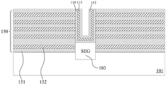
The method starts with a semiconductor structure in which a channel hole 102 and an epitaxial layer 103 have been formed, as shown in fig. 3 a.
In this step, an insulating stacked structure 150 formed by alternately stacking interlayer insulating layers 151 and sacrificial layers 152 on a substrate 101, a channel hole penetrating the insulating stacked structure 150, and an epitaxial Layer 103 at the bottom of the channel hole are formed using a Deposition process, such as Atomic Layer Deposition (ALD), physical Vapor Deposition (PVD), or Chemical Vapor Deposition (CVD). In this embodiment, the substrate 101 is, for example, a single crystal silicon substrate, the interlayer insulating layer 151 is, for example, composed of silicon oxide, and the sacrificial layer 152 is, for example, composed of silicon nitride. The sacrificial layer 152 will be replaced with a conductor layer in a subsequent gate formation process. The Epitaxial layer 103 may, for example, be a Selective Epitaxial Growth (SEG).
In the embodiment, the insulating stack structure shown includes 5 sacrificial layers 152, and the sacrificial layers 152 are set to other numbers according to different requirements of different 3D memory devices on the number of memory cells in the manufacturing process of a specific 3D memory device.
Further, functional layers are formed on the sidewalls of the channel holes 102, and the functional layers include a gate oxide layer 114, a charge storage layer 113 on the gate oxide layer, and a tunnel oxide layer 112 on the charge storage layer, as shown in fig. 3 b.
In this step, a gate oxide layer 114, a charge storage layer 113 and a tunnel oxide layer 112 are formed in the trench hole along the sidewalls and bottom thereof, and the selected material may be a single layer and/or multi-layer combination of oxide-nitride-oxide (ONO), but is not limited to the materials and combinations mentioned herein. In this embodiment, the gate oxide layer 114 and the tunnel oxide layer 112 are, for example, silicon oxide, and the charge storage layer 113 is, for example, silicon nitride. The gate oxide layer 114, the charge storage layer 113 and the tunnel oxide layer 112 are formed by a chemical vapor deposition process.
Further, the functional layer on the bottom of the channel hole 102 is etched to form a first opening 104 that is exposed or extends into the epitaxial layer 103, as shown in fig. 3 c.
In this step, an anisotropic dry etching process is used to etch the functional layer on the bottom of the trench hole. In one embodiment, the anisotropic dry etching process is a plasma etching process, and the gas used in the plasma etching process includes a fluorocarbon-containing gas.
Further, the charge storage layer 113 on the bottom of the channel hole 102 is removed to form a void 105, as shown in fig. 3 d.
In this step, the charge storage layer 113 at the bottom of the channel hole is removed by dry etching, which is anisotropic plasma etching in one embodiment. When the charge storage layer 113 at the bottom of the channel hole is removed, the charge storage layer 113 has a high etching selectivity ratio relative to the gate oxide layer 114 and the tunneling oxide layer 112, and the etching rate ratio of the charge storage layer 113 relative to the gate oxide layer 114 and the tunneling oxide layer 112 is at least greater than 30. Since the charge storage layer 113 is a nitride layer and the gate oxide layer 114 and the tunnel oxide layer 112 are oxide layers, the charge storage layer 113 at the bottom of the channel hole is removed by using an etching process with a High Etch selectivity (High Etch selectivity) for the nitride layer (e.g., silicon nitride SiN) and the oxide layer (e.g., silicon oxide), so that the gate oxide layer 114 and the tunnel oxide layer 112 at both sides of the first opening 104 are etched by a small amount.
Further, an oxide layer is formed on the surface of the functional layer, in the void 105, and on the sidewall and bottom surface of the first opening 104, as shown in fig. 3 e.
In this step, a tunnel oxide layer 112 is formed in the trench hole along the surface of the functional layer, in the void, and the sidewall and bottom surface of the first opening, so that the oxide layer at the bottom of the trench hole includes a gate oxide layer 114 and the tunnel oxide layer 112 on the gate oxide layer.
Further, a first channel layer 111a is formed on the functional layer and the oxide layer, as shown in fig. 3 f.
In this embodiment, the material of the first channel layer 111a is polysilicon. Further, the first channel layer 111a and the oxide layer on the bottom of the channel 102 are etched to form the second opening 106 exposed or extending into the epitaxial layer, the oxide layer including the gate oxide layer 114 and the tunnel oxide layer 112 on the gate oxide layer, as shown in fig. 3 g.
In this step, the first channel layer 111a and the oxide layer on the bottom of the channel hole are etched using anisotropic dry etching. In one embodiment, the anisotropic dry etching process is a plasma etching process, and the gas used in the plasma etching process includes a fluorocarbon-containing gas.
Further, a second channel layer 111b is formed on the surface of the first channel layer 111a and the bottom and sidewall surfaces of the second opening 106, as shown in fig. 3 h.
In this embodiment, the material of the second channel layer 111b is polysilicon, and the forming process is chemical vapor deposition. The second channel layer 111b and the first channel layer 111a together constitute the channel layer 111 of the NAND memory. At this time, the charge storage layer 113 is isolated from the channel layer 111.
Further, a filling layer 115 is formed on the channel layer 111 and the filling layer 115 on top of the channel hole 102 is removed to form a recess, in which a plug structure is formed, as shown in fig. 3 i.
In this embodiment, the material of the filling layer 115 is silicon oxide or other suitable materials. And depositing polysilicon in the groove to form a plug structure, wherein the plug structure is in contact with the channel layer.
Further, the plurality of sacrificial layers 152 are replaced with a plurality of gate conductors to form a gate stack structure 120, as shown in fig. 3j.
In this step, the sacrificial layer 152 is replaced with gate conductors 121, 122 and 123, thereby forming a gate stack structure 120. The material of the gate conductors 121, 122 and 123 may be metal or other conductive material (e.g., polysilicon, etc.). In this embodiment, the conductive material is a metal, and the metal is one or more of W, al, cu, ti, ag, au, pt, and Ni. Wherein the epitaxial layer 103 and the gate conductor 121 form a first select transistor; the channel layer 111 and gate conductor 122 form a plurality of memory transistors; the channel layer 111 and the gate conductor 123 form a second selection transistor.
The invention provides a 3D memory device and a method for fabricating the same,
forming a functional layer on the side wall and the bottom of the channel hole, wherein the functional layer comprises a gate oxide layer, a charge storage layer positioned on the gate oxide layer and a tunneling oxide layer positioned on the charge storage layer; removing the charge storage layer at the bottom of the channel hole; forming a channel layer on the functional layer; the charge storage layer is isolated from the channel layer at the corners of the functional layer, so that charges on the charge storage layer are prevented from leaking into the channel layer, and the stability of the threshold voltage of the bottom selection grid of the 3D memory is improved.
Other details of the 3D memory device, such as the structure of the memory array, the peripheral interconnections, etc., are not important to the present invention and will not be described herein.
In the context of the present invention, the three-dimensional memory device may be a 3D flash memory, such as a 3D nand flash memory.
Flow charts are used herein to illustrate operations performed by methods according to embodiments of the present application. It should be understood that the preceding operations are not necessarily performed in the exact order in which they are performed. Rather, various steps may be processed in reverse order or simultaneously. Meanwhile, other operations are added to or removed from these processes. For example, certain steps are not required and thus may be omitted or replaced with other steps.
The semiconductor structure formed by the above embodiments can be processed by the following conventional steps to obtain a three-dimensional memory device.
While embodiments in accordance with the invention have been described above, these embodiments are not intended to be exhaustive or to limit the invention to the precise embodiments described. Obviously, many modifications and variations are possible in light of the above teaching. The embodiments were chosen and described in order to best explain the principles of the invention and the practical application, to thereby enable others skilled in the art to best utilize the invention and various embodiments with various modifications as are suited to the particular use contemplated. The invention is limited only by the claims and their full scope and equivalents.
Claims (11)
1. A method of manufacturing a 3D memory device, comprising:
forming an insulating stack structure over a substrate, the insulating stack structure including a plurality of interlayer insulating layers and a plurality of sacrificial layers that are alternately stacked;
forming a plurality of channel pillars through the insulating stack structure, the step of forming the channel pillars comprising:
forming a plurality of channel holes through the insulating stack structure and a portion of the substrate;
forming an epitaxial layer at the bottom of the channel hole, wherein the epitaxial layer is in contact with the substrate; and
forming a functional layer on the side wall and the bottom of the channel hole, wherein the functional layer comprises a gate oxide layer, a charge storage layer positioned on the gate oxide layer and a tunneling oxide layer positioned on the charge storage layer;
removing the charge storage layer at the bottom of the channel hole;
forming a channel layer on the functional layer, wherein the channel layer is positioned above the epitaxial layer and is in contact with the epitaxial layer;
wherein the charge storage layer is isolated from the channel layer at corners of the functional layer.
2. The manufacturing method according to claim 1, wherein the steps of forming the functional layer on the sidewall and the bottom of the channel hole and removing the charge storage layer at the bottom of the channel hole comprise:
forming the functional layer on the side wall and the bottom of the channel hole;
etching the functional layer on the bottom of the channel hole to form a first opening exposing the epitaxial layer;
removing the charge storage layer at the bottom of the channel hole to form a gap;
and forming an oxide layer on the surface of the functional layer, in the gap and on the side wall and the bottom surface of the first opening.
3. The method of manufacturing of claim 2, wherein the step of forming the void comprises:
and when the charge storage layer at the bottom of the channel hole is removed, the charge storage layer has a high etching selection ratio relative to the gate oxide layer and the tunneling oxide layer.
4. The method of manufacturing according to claim 3, wherein the ratio of the etch rate of the charge storage layer to the gate oxide layer and the tunnel oxide layer is at least greater than 30.
5. The manufacturing method according to claim 2, wherein forming a channel layer on the functional layer comprises:
forming a first channel layer on the functional layer and the oxide layer;
etching the first channel layer and the oxide layer on the bottom of the channel hole to form a second opening exposing the epitaxial layer;
and forming a second channel layer on the surface of the first channel layer and the bottom and the side wall surface of the second opening.
6. The manufacturing method according to claim 1, characterized by further comprising:
forming a filling layer on the channel layer;
and removing the filling layer at the top of the channel hole to form a groove, and forming a plug structure in the groove.
7. The manufacturing method according to claim 1, further comprising:
the plurality of sacrificial layers are replaced with a plurality of gate conductors to form a gate stack structure.
8. A 3D memory device, comprising:
a substrate;
a gate stack structure over the substrate, the gate stack structure including a plurality of interlayer insulating layers and a plurality of gate conductors alternately stacked; and
the channel columns penetrate through the gate laminated structure and comprise epitaxial layers positioned at the bottoms of the channel columns, functional layers positioned on the side walls of the channel columns, oxide layers positioned on the functional layers and part of the epitaxial layers and channel layers positioned on the functional layers and the oxide layers;
the channel layer is positioned above the epitaxial layer and is in contact with the epitaxial layer;
the functional layer comprises a gate oxide layer, a charge storage layer positioned on the gate oxide layer and a tunneling oxide layer positioned on the charge storage layer; the charge storage layer is isolated from the channel layer at corners of the functional layer;
and a gate oxide layer and a tunneling oxide layer which are stacked in sequence are arranged between the charge storage layer and the epitaxial layer.
9. The 3D memory device of claim 8, wherein the charge storage layer has a high etch selectivity ratio with respect to the gate oxide layer and the tunnel oxide layer.
10. The 3D memory device of claim 9, wherein an etch rate ratio of the charge storage layer to the gate oxide layer and the tunnel oxide layer is at least greater than 30.
11. The 3D memory device of claim 8, further comprising:
a filler layer in the channel pillar, the filler layer in contact with the channel layer;
and the plug structure is positioned on the filling layer.
Priority Applications (2)
| Application Number | Priority Date | Filing Date | Title |
|---|---|---|---|
| CN202310036887.9A CN115968202A (en) | 2019-12-31 | 2019-12-31 | 3D memory device and method of manufacturing the same |
| CN201911421883.2A CN111180452B (en) | 2019-12-31 | 2019-12-31 | 3D memory device and method of manufacturing the same |
Applications Claiming Priority (1)
| Application Number | Priority Date | Filing Date | Title |
|---|---|---|---|
| CN201911421883.2A CN111180452B (en) | 2019-12-31 | 2019-12-31 | 3D memory device and method of manufacturing the same |
Related Child Applications (1)
| Application Number | Title | Priority Date | Filing Date |
|---|---|---|---|
| CN202310036887.9A Division CN115968202A (en) | 2019-12-31 | 2019-12-31 | 3D memory device and method of manufacturing the same |
Publications (2)
| Publication Number | Publication Date |
|---|---|
| CN111180452A CN111180452A (en) | 2020-05-19 |
| CN111180452B true CN111180452B (en) | 2023-01-24 |
Family
ID=70657661
Family Applications (2)
| Application Number | Title | Priority Date | Filing Date |
|---|---|---|---|
| CN201911421883.2A Active CN111180452B (en) | 2019-12-31 | 2019-12-31 | 3D memory device and method of manufacturing the same |
| CN202310036887.9A Pending CN115968202A (en) | 2019-12-31 | 2019-12-31 | 3D memory device and method of manufacturing the same |
Family Applications After (1)
| Application Number | Title | Priority Date | Filing Date |
|---|---|---|---|
| CN202310036887.9A Pending CN115968202A (en) | 2019-12-31 | 2019-12-31 | 3D memory device and method of manufacturing the same |
Country Status (1)
| Country | Link |
|---|---|
| CN (2) | CN111180452B (en) |
Families Citing this family (1)
| Publication number | Priority date | Publication date | Assignee | Title |
|---|---|---|---|---|
| CN111758159B (en) * | 2020-05-25 | 2021-04-27 | 长江存储科技有限责任公司 | Memory device and method of forming the same |
Family Cites Families (3)
| Publication number | Priority date | Publication date | Assignee | Title |
|---|---|---|---|---|
| KR102248205B1 (en) * | 2014-06-25 | 2021-05-04 | 삼성전자주식회사 | Semiconductor device having vertical channel and air gap |
| KR102611809B1 (en) * | 2018-09-13 | 2023-12-07 | 양쯔 메모리 테크놀로지스 씨오., 엘티디. | New 3D NAND memory device and method of forming it |
| CN109887927B (en) * | 2019-03-20 | 2021-03-30 | 长江存储科技有限责任公司 | Three-dimensional memory and manufacturing method thereof |
-
2019
- 2019-12-31 CN CN201911421883.2A patent/CN111180452B/en active Active
- 2019-12-31 CN CN202310036887.9A patent/CN115968202A/en active Pending
Also Published As
| Publication number | Publication date |
|---|---|
| CN115968202A (en) | 2023-04-14 |
| CN111180452A (en) | 2020-05-19 |
Similar Documents
| Publication | Publication Date | Title |
|---|---|---|
| CN111180451B (en) | 3D memory device and method of manufacturing the same | |
| CN110137178B (en) | 3D memory device and method of manufacturing the same | |
| CN109390348B (en) | 3D memory device and method of manufacturing the same | |
| CN111211130B (en) | 3D memory device and method of manufacturing the same | |
| CN109119424B (en) | 3D memory device and method of manufacturing the same | |
| CN109003982B (en) | 3D memory device and method of manufacturing the same | |
| CN113224079B (en) | 3D memory device and method of manufacturing the same | |
| CN110289259B (en) | 3D memory device and method of manufacturing the same | |
| CN110379812B (en) | 3D memory device and method of manufacturing the same | |
| CN110649033A (en) | 3D memory device and method of manufacturing the same | |
| CN110808254A (en) | 3D memory device and method of manufacturing the same | |
| CN110828469A (en) | 3D memory device and method of manufacturing the same | |
| CN110676257A (en) | 3D memory device and method of manufacturing the same | |
| CN111211128B (en) | 3D memory device and method of manufacturing the same | |
| CN110767656B (en) | 3D memory device and method of manufacturing the same | |
| CN109545793B (en) | 3D memory device and method of manufacturing the same | |
| CN110808252B (en) | 3D memory device and method of manufacturing the same | |
| CN111180452B (en) | 3D memory device and method of manufacturing the same | |
| CN109148453B (en) | Method of manufacturing semiconductor device and 3D memory device | |
| CN111370418B (en) | Method for manufacturing 3D memory device | |
| CN111384061B (en) | 3D memory device and method of manufacturing the same | |
| CN109449162B (en) | Manufacturing method of 3D memory device and 3D memory device | |
| CN109003984B (en) | 3D memory device and method of manufacturing the same | |
| CN113192962B (en) | Memory device and method of manufacturing the same | |
| CN113629059B (en) | Manufacturing method of 3D memory device and 3D memory device |
Legal Events
| Date | Code | Title | Description |
|---|---|---|---|
| PB01 | Publication | ||
| PB01 | Publication | ||
| SE01 | Entry into force of request for substantive examination | ||
| SE01 | Entry into force of request for substantive examination | ||
| GR01 | Patent grant | ||
| GR01 | Patent grant |