CN1105324C - Array base plate, liquid-crystal displaying device of thin-film transistor, and method for production of said base plate - Google Patents
Array base plate, liquid-crystal displaying device of thin-film transistor, and method for production of said base plate Download PDFInfo
- Publication number
- CN1105324C CN1105324C CN96107917A CN96107917A CN1105324C CN 1105324 C CN1105324 C CN 1105324C CN 96107917 A CN96107917 A CN 96107917A CN 96107917 A CN96107917 A CN 96107917A CN 1105324 C CN1105324 C CN 1105324C
- Authority
- CN
- China
- Prior art keywords
- pixel capacitors
- mentioned
- film
- electrode
- metallic pattern
- Prior art date
- Legal status (The legal status is an assumption and is not a legal conclusion. Google has not performed a legal analysis and makes no representation as to the accuracy of the status listed.)
- Expired - Fee Related
Links
- 239000004973 liquid crystal related substance Substances 0.000 title claims abstract description 57
- 238000004519 manufacturing process Methods 0.000 title claims abstract description 27
- 239000010409 thin film Substances 0.000 title claims abstract description 21
- 238000000034 method Methods 0.000 claims abstract description 160
- 239000010408 film Substances 0.000 claims abstract description 108
- 230000007547 defect Effects 0.000 claims abstract description 92
- 230000008439 repair process Effects 0.000 claims abstract description 43
- 239000003990 capacitor Substances 0.000 claims description 107
- 230000015572 biosynthetic process Effects 0.000 claims description 46
- 238000001259 photo etching Methods 0.000 claims description 46
- 230000008569 process Effects 0.000 claims description 46
- 238000004544 sputter deposition Methods 0.000 claims description 27
- 229910052804 chromium Inorganic materials 0.000 claims description 26
- 239000000758 substrate Substances 0.000 claims description 25
- 239000004065 semiconductor Substances 0.000 claims description 23
- 229910052715 tantalum Inorganic materials 0.000 claims description 20
- 230000005855 radiation Effects 0.000 claims description 19
- 229910052719 titanium Inorganic materials 0.000 claims description 16
- 239000011248 coating agent Substances 0.000 claims description 14
- 238000000576 coating method Methods 0.000 claims description 14
- 238000005229 chemical vapour deposition Methods 0.000 claims description 13
- 229910052751 metal Inorganic materials 0.000 claims description 13
- 239000002184 metal Substances 0.000 claims description 13
- 230000004927 fusion Effects 0.000 claims description 12
- 238000003860 storage Methods 0.000 claims description 12
- 229910052782 aluminium Inorganic materials 0.000 claims description 8
- 239000007769 metal material Substances 0.000 claims description 6
- 229910052750 molybdenum Inorganic materials 0.000 claims description 4
- 239000003870 refractory metal Substances 0.000 claims description 4
- 229910052721 tungsten Inorganic materials 0.000 claims description 3
- 230000008878 coupling Effects 0.000 claims description 2
- 238000010168 coupling process Methods 0.000 claims description 2
- 238000005859 coupling reaction Methods 0.000 claims description 2
- 238000009413 insulation Methods 0.000 claims 6
- 229910021417 amorphous silicon Inorganic materials 0.000 description 42
- 238000005268 plasma chemical vapour deposition Methods 0.000 description 15
- 239000011521 glass Substances 0.000 description 9
- AMGQUBHHOARCQH-UHFFFAOYSA-N indium;oxotin Chemical compound [In].[Sn]=O AMGQUBHHOARCQH-UHFFFAOYSA-N 0.000 description 9
- 229920005591 polysilicon Polymers 0.000 description 9
- 230000004888 barrier function Effects 0.000 description 8
- 238000005530 etching Methods 0.000 description 8
- 230000000694 effects Effects 0.000 description 7
- 239000000463 material Substances 0.000 description 7
- 229910021420 polycrystalline silicon Inorganic materials 0.000 description 7
- 230000001678 irradiating effect Effects 0.000 description 6
- 230000002950 deficient Effects 0.000 description 4
- 230000008018 melting Effects 0.000 description 4
- 238000002844 melting Methods 0.000 description 4
- 238000003698 laser cutting Methods 0.000 description 3
- 230000008901 benefit Effects 0.000 description 2
- 230000008859 change Effects 0.000 description 2
- 230000007257 malfunction Effects 0.000 description 2
- 229910004298 SiO 2 Inorganic materials 0.000 description 1
- XUIMIQQOPSSXEZ-UHFFFAOYSA-N Silicon Chemical compound [Si] XUIMIQQOPSSXEZ-UHFFFAOYSA-N 0.000 description 1
- 239000012467 final product Substances 0.000 description 1
- 239000012212 insulator Substances 0.000 description 1
- 229910044991 metal oxide Inorganic materials 0.000 description 1
- 150000004706 metal oxides Chemical class 0.000 description 1
- 229910052710 silicon Inorganic materials 0.000 description 1
- 239000010703 silicon Substances 0.000 description 1
Images


Classifications
-
- G—PHYSICS
- G02—OPTICS
- G02F—OPTICAL DEVICES OR ARRANGEMENTS FOR THE CONTROL OF LIGHT BY MODIFICATION OF THE OPTICAL PROPERTIES OF THE MEDIA OF THE ELEMENTS INVOLVED THEREIN; NON-LINEAR OPTICS; FREQUENCY-CHANGING OF LIGHT; OPTICAL LOGIC ELEMENTS; OPTICAL ANALOGUE/DIGITAL CONVERTERS
- G02F1/00—Devices or arrangements for the control of the intensity, colour, phase, polarisation or direction of light arriving from an independent light source, e.g. switching, gating or modulating; Non-linear optics
- G02F1/01—Devices or arrangements for the control of the intensity, colour, phase, polarisation or direction of light arriving from an independent light source, e.g. switching, gating or modulating; Non-linear optics for the control of the intensity, phase, polarisation or colour
- G02F1/13—Devices or arrangements for the control of the intensity, colour, phase, polarisation or direction of light arriving from an independent light source, e.g. switching, gating or modulating; Non-linear optics for the control of the intensity, phase, polarisation or colour based on liquid crystals, e.g. single liquid crystal display cells
- G02F1/133—Constructional arrangements; Operation of liquid crystal cells; Circuit arrangements
- G02F1/136—Liquid crystal cells structurally associated with a semi-conducting layer or substrate, e.g. cells forming part of an integrated circuit
- G02F1/1362—Active matrix addressed cells
- G02F1/136259—Repairing; Defects
-
- G—PHYSICS
- G02—OPTICS
- G02F—OPTICAL DEVICES OR ARRANGEMENTS FOR THE CONTROL OF LIGHT BY MODIFICATION OF THE OPTICAL PROPERTIES OF THE MEDIA OF THE ELEMENTS INVOLVED THEREIN; NON-LINEAR OPTICS; FREQUENCY-CHANGING OF LIGHT; OPTICAL LOGIC ELEMENTS; OPTICAL ANALOGUE/DIGITAL CONVERTERS
- G02F1/00—Devices or arrangements for the control of the intensity, colour, phase, polarisation or direction of light arriving from an independent light source, e.g. switching, gating or modulating; Non-linear optics
- G02F1/01—Devices or arrangements for the control of the intensity, colour, phase, polarisation or direction of light arriving from an independent light source, e.g. switching, gating or modulating; Non-linear optics for the control of the intensity, phase, polarisation or colour
- G02F1/13—Devices or arrangements for the control of the intensity, colour, phase, polarisation or direction of light arriving from an independent light source, e.g. switching, gating or modulating; Non-linear optics for the control of the intensity, phase, polarisation or colour based on liquid crystals, e.g. single liquid crystal display cells
- G02F1/133—Constructional arrangements; Operation of liquid crystal cells; Circuit arrangements
- G02F1/136—Liquid crystal cells structurally associated with a semi-conducting layer or substrate, e.g. cells forming part of an integrated circuit
- G02F1/1362—Active matrix addressed cells
- G02F1/136286—Wiring, e.g. gate line, drain line
-
- G—PHYSICS
- G02—OPTICS
- G02F—OPTICAL DEVICES OR ARRANGEMENTS FOR THE CONTROL OF LIGHT BY MODIFICATION OF THE OPTICAL PROPERTIES OF THE MEDIA OF THE ELEMENTS INVOLVED THEREIN; NON-LINEAR OPTICS; FREQUENCY-CHANGING OF LIGHT; OPTICAL LOGIC ELEMENTS; OPTICAL ANALOGUE/DIGITAL CONVERTERS
- G02F1/00—Devices or arrangements for the control of the intensity, colour, phase, polarisation or direction of light arriving from an independent light source, e.g. switching, gating or modulating; Non-linear optics
- G02F1/01—Devices or arrangements for the control of the intensity, colour, phase, polarisation or direction of light arriving from an independent light source, e.g. switching, gating or modulating; Non-linear optics for the control of the intensity, phase, polarisation or colour
- G02F1/13—Devices or arrangements for the control of the intensity, colour, phase, polarisation or direction of light arriving from an independent light source, e.g. switching, gating or modulating; Non-linear optics for the control of the intensity, phase, polarisation or colour based on liquid crystals, e.g. single liquid crystal display cells
- G02F1/133—Constructional arrangements; Operation of liquid crystal cells; Circuit arrangements
- G02F1/136—Liquid crystal cells structurally associated with a semi-conducting layer or substrate, e.g. cells forming part of an integrated circuit
- G02F1/1362—Active matrix addressed cells
- G02F1/1368—Active matrix addressed cells in which the switching element is a three-electrode device
-
- H—ELECTRICITY
- H01—ELECTRIC ELEMENTS
- H01L—SEMICONDUCTOR DEVICES NOT COVERED BY CLASS H10
- H01L27/00—Devices consisting of a plurality of semiconductor or other solid-state components formed in or on a common substrate
- H01L27/02—Devices consisting of a plurality of semiconductor or other solid-state components formed in or on a common substrate including semiconductor components specially adapted for rectifying, oscillating, amplifying or switching and having at least one potential-jump barrier or surface barrier; including integrated passive circuit elements with at least one potential-jump barrier or surface barrier
- H01L27/12—Devices consisting of a plurality of semiconductor or other solid-state components formed in or on a common substrate including semiconductor components specially adapted for rectifying, oscillating, amplifying or switching and having at least one potential-jump barrier or surface barrier; including integrated passive circuit elements with at least one potential-jump barrier or surface barrier the substrate being other than a semiconductor body, e.g. an insulating body
- H01L27/1214—Devices consisting of a plurality of semiconductor or other solid-state components formed in or on a common substrate including semiconductor components specially adapted for rectifying, oscillating, amplifying or switching and having at least one potential-jump barrier or surface barrier; including integrated passive circuit elements with at least one potential-jump barrier or surface barrier the substrate being other than a semiconductor body, e.g. an insulating body comprising a plurality of TFTs formed on a non-semiconducting substrate, e.g. driving circuits for AMLCDs
-
- H—ELECTRICITY
- H01—ELECTRIC ELEMENTS
- H01L—SEMICONDUCTOR DEVICES NOT COVERED BY CLASS H10
- H01L29/00—Semiconductor devices adapted for rectifying, amplifying, oscillating or switching, or capacitors or resistors with at least one potential-jump barrier or surface barrier, e.g. PN junction depletion layer or carrier concentration layer; Details of semiconductor bodies or of electrodes thereof ; Multistep manufacturing processes therefor
- H01L29/66—Types of semiconductor device ; Multistep manufacturing processes therefor
- H01L29/68—Types of semiconductor device ; Multistep manufacturing processes therefor controllable by only the electric current supplied, or only the electric potential applied, to an electrode which does not carry the current to be rectified, amplified or switched
- H01L29/76—Unipolar devices, e.g. field effect transistors
- H01L29/772—Field effect transistors
- H01L29/78—Field effect transistors with field effect produced by an insulated gate
- H01L29/786—Thin film transistors, i.e. transistors with a channel being at least partly a thin film
-
- G—PHYSICS
- G02—OPTICS
- G02F—OPTICAL DEVICES OR ARRANGEMENTS FOR THE CONTROL OF LIGHT BY MODIFICATION OF THE OPTICAL PROPERTIES OF THE MEDIA OF THE ELEMENTS INVOLVED THEREIN; NON-LINEAR OPTICS; FREQUENCY-CHANGING OF LIGHT; OPTICAL LOGIC ELEMENTS; OPTICAL ANALOGUE/DIGITAL CONVERTERS
- G02F1/00—Devices or arrangements for the control of the intensity, colour, phase, polarisation or direction of light arriving from an independent light source, e.g. switching, gating or modulating; Non-linear optics
- G02F1/01—Devices or arrangements for the control of the intensity, colour, phase, polarisation or direction of light arriving from an independent light source, e.g. switching, gating or modulating; Non-linear optics for the control of the intensity, phase, polarisation or colour
- G02F1/13—Devices or arrangements for the control of the intensity, colour, phase, polarisation or direction of light arriving from an independent light source, e.g. switching, gating or modulating; Non-linear optics for the control of the intensity, phase, polarisation or colour based on liquid crystals, e.g. single liquid crystal display cells
- G02F1/133—Constructional arrangements; Operation of liquid crystal cells; Circuit arrangements
- G02F1/136—Liquid crystal cells structurally associated with a semi-conducting layer or substrate, e.g. cells forming part of an integrated circuit
- G02F1/1362—Active matrix addressed cells
- G02F1/136231—Active matrix addressed cells for reducing the number of lithographic steps
-
- G—PHYSICS
- G02—OPTICS
- G02F—OPTICAL DEVICES OR ARRANGEMENTS FOR THE CONTROL OF LIGHT BY MODIFICATION OF THE OPTICAL PROPERTIES OF THE MEDIA OF THE ELEMENTS INVOLVED THEREIN; NON-LINEAR OPTICS; FREQUENCY-CHANGING OF LIGHT; OPTICAL LOGIC ELEMENTS; OPTICAL ANALOGUE/DIGITAL CONVERTERS
- G02F1/00—Devices or arrangements for the control of the intensity, colour, phase, polarisation or direction of light arriving from an independent light source, e.g. switching, gating or modulating; Non-linear optics
- G02F1/01—Devices or arrangements for the control of the intensity, colour, phase, polarisation or direction of light arriving from an independent light source, e.g. switching, gating or modulating; Non-linear optics for the control of the intensity, phase, polarisation or colour
- G02F1/13—Devices or arrangements for the control of the intensity, colour, phase, polarisation or direction of light arriving from an independent light source, e.g. switching, gating or modulating; Non-linear optics for the control of the intensity, phase, polarisation or colour based on liquid crystals, e.g. single liquid crystal display cells
- G02F1/133—Constructional arrangements; Operation of liquid crystal cells; Circuit arrangements
- G02F1/136—Liquid crystal cells structurally associated with a semi-conducting layer or substrate, e.g. cells forming part of an integrated circuit
- G02F1/1362—Active matrix addressed cells
- G02F1/136259—Repairing; Defects
- G02F1/136263—Line defects
-
- G—PHYSICS
- G02—OPTICS
- G02F—OPTICAL DEVICES OR ARRANGEMENTS FOR THE CONTROL OF LIGHT BY MODIFICATION OF THE OPTICAL PROPERTIES OF THE MEDIA OF THE ELEMENTS INVOLVED THEREIN; NON-LINEAR OPTICS; FREQUENCY-CHANGING OF LIGHT; OPTICAL LOGIC ELEMENTS; OPTICAL ANALOGUE/DIGITAL CONVERTERS
- G02F1/00—Devices or arrangements for the control of the intensity, colour, phase, polarisation or direction of light arriving from an independent light source, e.g. switching, gating or modulating; Non-linear optics
- G02F1/01—Devices or arrangements for the control of the intensity, colour, phase, polarisation or direction of light arriving from an independent light source, e.g. switching, gating or modulating; Non-linear optics for the control of the intensity, phase, polarisation or colour
- G02F1/13—Devices or arrangements for the control of the intensity, colour, phase, polarisation or direction of light arriving from an independent light source, e.g. switching, gating or modulating; Non-linear optics for the control of the intensity, phase, polarisation or colour based on liquid crystals, e.g. single liquid crystal display cells
- G02F1/133—Constructional arrangements; Operation of liquid crystal cells; Circuit arrangements
- G02F1/136—Liquid crystal cells structurally associated with a semi-conducting layer or substrate, e.g. cells forming part of an integrated circuit
- G02F1/1362—Active matrix addressed cells
- G02F1/136259—Repairing; Defects
- G02F1/136272—Auxiliary lines
Abstract
To provide a liquid crystal display device with which the sure repair of a pixel failing to operate normally, i.e., dot defect, in the TFT array of the liquid crystal display device is possible and its production and a method for repairing the dot defect. Bridges 13 which bestride adjacent pixel electrodes 3 and consist of metallic thin films and islands 12 which consist of the metallic thin films in the positions corresponding to the lower layers of these bridges 13 via gate insulating films and the positions of the upper layers or the lower layers of the pixel electrodes 3 are formed in this liquid crystal display device. If the certain pixel includes the dot defect, the gate insulating film between the bridge 13 and the island 12 is melted by a laser beam to short-circuit the bridge 13 and the island 12, by which the pixel including the dot defect is made into the same potential as the potential of the adjacent pixels and is thereby repaired.
Description
The invention provides TFT (thin film transistor (TFT)) array base palte, use the manufacture method of the liquid crystal indicator and the tft array substrate of this substrate, the restorative procedure of point defect (it is to make one of principal element that yield rate reduces) particularly is provided.
The sort of device that is shown in Figure 25 and 26 is arranged in the tft array that existing liquid crystal indicator adopted.
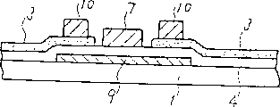
Figure 25 is the local expanded view of tft array used in the available liquid crystal display device, and Figure 26 is the A-A sectional drawing among Figure 25.In the drawings, the 1st, glass substrate, the 2nd, have the grid wiring of gate electrode concurrently, the 3rd, the pixel capacitors that constitutes by nesa coating, the 4th, gate insulating film, the 5th, semiconductor layer, the 6th, ohmic contact layer, the 7th, source electrode and wiring, 8 are drain electrode.
The manufacturing process and the structure of existing tft array are described earlier.At first, on the glass substrate that cleaned, form the metallic film of the element of Cr, Ta, Ti, and it is formed figure, and then form gate electrode and wiring 2 with methods such as photoetching processes with methods such as sputtering methods.Secondly, with SiN or the SiO of formation such as plasma CVD (chemical vapour deposition) method as gate insulating film 4
2Deng dielectric film, as the i-a-Si of semiconductor layer 5 or polysilicon etc., and as the film of n-a-Si of ohmic contact layer 6 etc.Secondly, make n-a-Si and i-a-Si form island or threadlike graph with methods such as photoetching processes.Secondly, the method with sputter etc. forms the nesa coating that ITO (indium tin oxide) waits, and formation pixel capacitors 3.Form the metallic film of Al, Cr etc. again with sputtering method etc., and it formed figure with photoetching process etc., the source of formation electrode and connect up 7 and drain electrode 8 after, the n-a-Si that is in the formation ohmic contact layer 6 between source-leakage is degraded.At last, as required with formation diaphragms such as SiN.
In addition, in existing this liquid crystal indicator, be shown in the sort of array of Figure 27 and Figure 28 in the used tft array in addition.Figure 27 is the partial plan layout of tft array used in the existing liquid crystal indicator.The B-B sectional drawing of Figure 28 and Figure 27.The manufacturing process and the structure of existing tft array are described according to these figure now.
Be shown in the existing tft array of Figure 27 and Figure 28, at first on the substrate 1 that cleaned, form the metallic film of Cr, Ta, Ti etc. with the method for sputtering method and so on, and it is formed required figure with the method for photoetching and so on, to form gate electrode (and grid wiring) 2.Secondly, form the nesa coating that ITO (indium tin oxide) waits with methods such as sputters, and with the method for photoetching or the like the required figure of its formation, with formation pixel capacitors 3.Secondly, with plasma CVD (chemical vapour deposition) method etc. form as gate insulating film 4, for example by SiO
2, the dielectric film that constitutes such as SiN, metal oxide film, as the i-a-Si of semiconductor layer 5 or polysilicon etc. and as the films such as n-a-Si of ohmic contact layer 6.Secondly with the method for photoetching process etc., n-a-Si and i-a-Si are formed the figure of island (being shown in the part of the sort of island of the semiconductor layer 5 of Fig. 1) and wire (part of elongated band shape).
Method with photoetching process etc. forms required figure to form contact hole (part that drain electrode 8 is connected with pixel capacitors) 9 on pixel capacitors again.Secondly with methods such as sputtering methods it is formed figure to form source electrode (and source wiring) 7 and drain electrode 8.Secondly, degrade the n-a-Si that is in (on the top of the semiconductor layer 5 that is shown in Fig. 4 and not by the part that either party covered of source electrode and drain electrode) between source electrode and the drain electrode.At last, as required with formation diaphragms such as SiN.
In the tft array that aforesaid way constitutes, because of foreign matter etc. makes gate electrode 2 and drain electrode 8 short circuits, perhaps because of the pixel of the former thereby cisco unity malfunction of the insufficient grade of Ohmic contact, promptly so-called point defect will produce with the probability of several ppm.As the method for repairing this defective, open clear 59-101693 communique or the spy opens shown in the flat 2-134320 communique as the spy, have to form earlier and make the figure that couples together between the drive electrode that adjoins mutually, use laser radiation again, the pixel capacitors that forms defective is connected to the method for adjoining pixel capacitors.
Figure 29 is the partial enlarged drawing of the tft array with memory capacitance used in the existing liquid crystal indicator, and Figure 30 is the A-A sectional drawing among Figure 29.Among the figure, the 1st, glass substrate, the 21st, storage capacitor electrode, the 31st, the dielectric of memory capacitance.
Secondly, manufacturing process and the structure to such existing tft array describes.At first, on the glass substrate 1 that had cleaned, form the metallic film of Cr, Ta, Ti etc., with methods such as photoetching processes it is formed figure to form storage capacitor electrode 21 again with methods such as sputtering methods.Secondly, with SiN or the SiO of formation such as plasma CVD (chemical vapour deposition) method as the dielectric film 31 of memory capacitance
2Deng film.Then, be formed for figure with the gate electrode that will form later on and grid wiring 2 contacted contact holes etc.Secondly, form the metallic film of Cr, Ta, Ti and so on, and make it to form figure, to form gate electrode and grid wiring 2 with methods such as photoetching with methods such as sputters.Form the transparent conductive film that ITO (indium tin oxide) waits with methods such as sputters again, and form figure with formation pixel capacitors 3 with methods such as photoetching.
Secondly, with SiN or the SiO of methods such as plasma CVD method formation as gate insulating film 4
2And so on dielectric film, as the i-a-Si of semiconductor layer 5 or polysilicon etc. and as the films such as n-a-Si of ohmic contact layer 6.Secondly, the method with photoetching etc. forms island or threadlike graph to n-a-Si and i-a-Si.Secondly, form figure, form contact hole with top in pixel capacitors 3 with the method for photoetching process etc.With the metallic film of formation Al, Cr etc. such as sputtering method, with after formation source electrode and source wiring 7 and the drain electrode 8, degrade the n-a-Si that is between source-leakage again with formation figures such as photoetching processes.At last, as required with formation diaphragms such as SiN.
In the tft array that aforesaid way constitutes,, perhaps produce the pixel of cisco unity malfunction, promptly so-called point defect with the probability of several ppm because of the reason of Ohmic contact imperfection etc. perhaps because of foreign matter etc. makes gate electrode 2 and drain electrode 8 short circuits.As the method for repairing this defective, open flat 2-284120 communique and the spy opens shown in the flat 5-66415 communique as the spy, the figure that couples together between forming the drive electrode that adjoins mutually when forming memory capacitance is arranged, and make it fusion, the pixel capacitors that becomes defective is connected to the method that the pixel capacitors of adjoining mutually gets on laser radiation.
As mentioned above, in existing tft array, the generation that exists because of point defect makes the low problem of yield rate.In addition, in existing point defect restorative procedure, though had the connection figure that is used to repair point defect, but when using laser radiation with connection and this figure neighboring pixels electrode, exist when pixel electrode one side is shone, because of pixel capacitors is transparent, thereby laser-transmitting goes over, so be difficult to fully and the problem that figure connects that is connected that is used to repair.
Moreover, carry out laser radiation even also exist, fusion connects situation of figure or the like reliably, thereby the problem that is difficult to repair.
In addition, in existing point defect restorative procedure, though had the figure that is used to repair point defect, but under situation with laser radiation connection and this figure neighboring pixels electrode, exist because pixel capacitors is transparent, thereby laser-transmitting goes over, and the problem that is difficult to connect fully.
Therefore, content of the present invention comprises: have use form simultaneously with gate electrode and grid wiring identical materials, repair figure and repair on figure by getting involved the island that gate insulating film forms in the point defect of carrying out repetition on two pixels that adjoin in this point defect; For the pixel that is identified as point defect, first transistor part with this pixel of laser cutting, and then irradiating laser couple together the pixel capacitors of the pixel that adjoins by getting involved point defect reparation figure to each other.
In addition, content of the present invention also comprises: have use form simultaneously with the memory capacitance identical materials, repair figure and repair on figure by getting involved the island that the memory capacitance dielectric film forms in the point defect that repeats on two pixels that adjoin in this point defect; For the pixel that is identified as point defect, with the transistor part of this pixel of laser cutting, shine again earlier with laser, by getting involved point defect reparation figure the pixel capacitors of adjoining pixel is coupled together each other.
In this case, couple together owing to making two metal films (being that point defect is repaired figure) of getting involved dielectric film with laser and being connected to the island that forms on the pixel capacitors, so can repair easily and reliably.
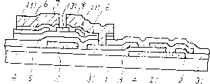
Fig. 1 is a partial plan layout, the figure shows tft array used in the liquid crystal indicator of embodiments of the invention 1.
Fig. 2 is the A-A sectional drawing of Fig. 1.
Fig. 3 is the B-B sectional drawing of Fig. 1.
Fig. 4 is a schematic partial sectional view.It shows tft array used in the liquid crystal indicator of embodiments of the invention 2.
Fig. 5 is a partial plan layout, and it shows tft array used in the liquid crystal indicator of embodiments of the invention 3.
Fig. 6 is the A-A sectional drawing of Fig. 5.
Fig. 7 is the B-B sectional drawing of Fig. 5.
Fig. 8 is a schematic partial sectional view, and it shows tft array used in the liquid crystal indicator of embodiments of the invention 4.
Fig. 9 is a partial plan layout, and it shows tft array used in the display device of the 5th embodiment of the present invention.
Figure 10 is the A-A sectional drawing of Fig. 9.
Figure 11 is the B-B sectional drawing of Fig. 9.
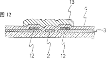
Figure 12 is the sectional drawing of tft array used in the display device of embodiments of the invention 6.
Figure 13 is the partial plan layout of tft array used in the display device of embodiments of the invention 7.
Figure 14 is the A-A sectional drawing of Figure 13.
Figure 15 is the B-B sectional drawing of Figure 13.
Figure 16 is a tft array sectional drawing used in the display device of embodiments of the invention 8.
Figure 17 is the partial plan layout of tft array used in the liquid crystal indicator of embodiments of the invention 9.
Figure 18 is the A-A sectional drawing of Figure 17.
Figure 19 is the B-B sectional drawing of Figure 17.
Figure 20 is a schematic partial sectional view, and it shows tft array used in the liquid crystal indicator of embodiments of the invention 10.
Figure 21 is a partial plan layout, and it shows tft array used in the liquid crystal indicator of embodiments of the invention 11.
Figure 22 is the A-A sectional drawing of Figure 21.
Figure 23 is the B-B sectional drawing of Figure 21.
Figure 24 is that local section illustrates tft array used in the liquid crystal indicator of embodiments of the invention 12.
The part plan of Figure 25 illustrates tft array used in the available liquid crystal display device.
Figure 26 is the A-A sectional drawing of Figure 25.
Figure 27 is the partial plan layout of TFT used in the existing liquid crystal indicator.
Figure 28 is the B-B sectional drawing of Figure 27.
The part plan of Figure 29 illustrates tft array used in the existing liquid crystal indicator.
Figure 30 is the A-A sectional drawing of Figure 29.
Embodiment
With reference to description of drawings embodiments of the invention 1.Fig. 1 is the partial plan layout of tft array used in the liquid crystal indicator of the present invention, and Fig. 2 is the A-A sectional drawing of Fig. 1, and Fig. 3 is the B-B sectional drawing of Fig. 1.In the drawings, the 9th, the point defect of conduct the 1st metallic pattern that forms simultaneously with gate electrode and grid wiring 2 identical materials is repaired figure, the 10th, use the island with source electrode and wiring 7 and conduct the 2nd metallic pattern that forms simultaneously of drain electrode 8 identical materials, and island 10 is formed and is connected on the pixel capacitors 3.The position of laser radiation when in addition, C-C and D represent to carry out the point defect reparation among the figure.In addition, give identical symbol and save explanation for the part identical with conventional example.
Manufacture method to the tft array in the present embodiment describes.At first, on the glass substrate 1 that had cleaned, form the high melting point metal film of Cr, Ta, the Ti etc. of the about 300nm of thickness with methods such as sputtering methods, and make it to form figure, to form gate electrode and wiring 2 and point defect reparation figure 9 with methods such as photoetching processes.Secondly, use SiN or the SiO of the about 300nm of formation thickness such as plasma CVD (chemical vapour deposition) method as gate insulating film 4
2Deng dielectric film, as films such as the i-a-Si of the about 200nm of thickness of semiconductor layer 5 or polysilicons, and the films such as n-a-Si of the about 50nm of thickness as ohmic contact layer 6.Secondly, with methods such as photoetching processes n-a-Si and i-a-Si are formed the figure of island or wire.
Form the nesa coating of the ITO (indium tin oxide) etc. of the about 100nm of thickness again with the method for sputter etc., and make it to form figure with formation pixel capacitors 3 with the method for photoetching process etc.Then form the metallic film of Al, the Cr of the about 400nm of thickness or Mo etc. with sputtering method etc., make it to form figure with photoetching process etc., to form source electrode and wiring 7, drain electrode 8, repairing formation island 10 on the part that figure 9 is connected with point defect again, i.e. D place, laser radiation position when repairing point defect, repair figure 9 tops in point defect, by getting involved gate insulating film 4 and pixel capacitors 3 formation islands 10.Afterwards, degrade the n-a-Si that is between source-leakage.At last, as required, with formation diaphragms such as SiN.
In the liquid crystal indicator of the above tft array of making like this and this array of application, for the pixel that is identified as point defect, earlier partly cut off the transistor part of this pixel at the C-C line shown in Fig. 1 with laser, then, to the D on the pixel capacitors 3 part with adjoin D part irradiating laser on the pixel capacitors 3 of pixel, repair the pixel capacitors short circuit each other that figure 9 makes the pixel that adjoins mutually by point defect.Make it to be connected with laser owing to got involved two metal films (being that point defect is repaired figure 9 and island 10) of dielectric film, so reparation is able to easily and carries out reliably.Be effective particularly to laser radiation from pixel capacitors 3 one sides.In addition, repair figure 9 owing to form point defect with the metal of Cr, Ta, Ti etc., so compare when forming with waiting with silicon thin film, the fusion during laser radiation, connection are easy.Also have, be that the pixel capacitors about making connects in the formation in the present embodiment, but pixel capacitors is up and down connected.
If employing present embodiment, thereby then make pixel that is identified as point defect and the pixel short circuit of adjoining make the pixel capacitors current potential that adjoins each other become the identical identical demonstration of carrying out by utilizing point defect to repair figure, so be difficult for being counted as point defect, thereby improved the yield rate of tft array.In addition, in the present embodiment,, only be to have changed figure because usefulness is manufacture method same as the prior art, need not increase the advantage that operation number and cost can not uprise so have.
In addition, if do not use the present invention, the point defect of much less being found then in the tft array stage, even formed this tft array substrate and have transparency electrode and colored filter etc. accompany the liquid crystal indicator of liquid crystal between the electrode base board in opposite directions after, promptly under the situation of pixel capacitors one side incident laser, also can repair easily and reliably.
Fig. 4 is a schematic partial sectional view, and it shows used tft array in the display device as embodiments of the invention 2.Present embodiment is removed outside the order of the manufacturing process that has changed pixel capacitors 3 and source electrode and wiring 7 and drain electrode 8, and structure is identical with embodiment 1.Promptly repair figure 9 tops in point defect and getting involved formation island 10 under the situation of dielectric film, 10 tops form pixel capacitors 3 on the island again.Like this, island 10 is in the top of pixel capacitors 3 or following all right, no matter be any structure, all utilisation point defect repair figure 9 is repaired point defect easily and reliably, has obtained the effect identical with embodiment 1.
With reference to description of drawings embodiments of the invention 3.Fig. 5 is the partial plan layout of tft array used in the display device of the present invention, and Fig. 6 is the A-A sectional drawing of Fig. 5, the B-B sectional drawing that Fig. 7 is Fig. 5.Among the figure, the 11st, the etching barrier film.
Manufacture method to the tft array in the present embodiment describes.At first, on the substrate 1 that had cleaned, form the high melting point metal films such as Cr, Ta, Ti of the about 300nm of thickness with methods such as sputtering methods, make it to form figure with methods such as photoetching processes again,, form point defect reparation figure 9 again to form gate electrode and wiring 2.Secondly, use SiN or the SiO of the about 300nm of formation thickness such as plasma CVD (chemical vapour deposition) method as gate insulating film 4
2Deng SiN or the SiO of dielectric film, the about 100nm of thickness as etching barrier film 11 as the i-a-Si of semiconductor layer 5 or polysilicon etc. and the about 200nm of thickness
2Deng dielectric film.Secondly, with methods such as photoetching processes, make the etching barrier film form figure.Then, with formation such as plasma CVD methods as the n-a-Si of ohmic contact layer 6 and make it to form figure.
Form the nesa coating of the ITO (indium tin oxide) etc. of the about 100nm of thickness again with the method for sputter etc.In order to obtain as the desired briliancy of liquid crystal indicator, this thickness is 150nm to the maximum.Make this film form figure with methods such as photoetching processes to form pixel capacitors 3.Secondly, form the metallic film of Al, the Cr of the about 400nm of thickness or Mo etc. with methods such as sputtering methods, make it to form figure with photoetching process etc.,, form island 10 repairing on the part that figure 9 is connected again with point defect to form source electrode and wiring 7 and drain electrode 8.At last, as required with formation diaphragms such as SiN.
At the above tft array that makes in this wise and having used in its liquid crystal indicator, for identified be the pixel of point defect, use the transistor part of its pixel of laser cutting earlier, afterwards, again to the D on the pixel capacitors 3 part with adjoin D part irradiating laser on the pixel capacitors 3 of pixel, and repair the pixel capacitors short circuit that figure 9 makes the pixel that adjoins by point defect.
Even if in the tft array of above-mentioned this structure, also can obtain and embodiment 1 and 2 same effects.
The local section of Fig. 8 illustrates used tft array in the liquid crystal indicator in the embodiments of the invention 4.Present embodiment is except changing the pixel capacitors 3 and the order of the manufacturing process of source electrode and wiring 7 and drain electrode 8, and structure is identical with embodiment 3.That is,, form island 10 by getting involved dielectric film, and form pixel capacitors 3 above that in the top that point defect is repaired figure 9.Even this structure also can utilize point defect to repair figure 9, repair point defect easily and reliably, obtain the effect identical with embodiment 1-3.
In addition, the structure of the tft array shown in is nothing but an example in the above-described embodiments, and the present invention is not subjected to the restriction of these structures.
As mentioned above, if employing the present invention, then by adopting the way that makes the 1st metallic pattern that on two pixels that adjoin mutually, repeats and the 2nd metallic pattern fusion that on the 1st metallic pattern, forms with laser radiation in the mode that gets involved gate insulating film, just can obtain can be easily and repair the tft array substrate of picture element defect reliably and use the liquid crystal indicator of this tft array substrate, has the effect that improves yield rate.
In addition, owing to respectively the 1st metallic pattern and grid wiring, the 2nd metallic pattern and source and drain electrode are side by side formed with same metal material, so the process number of making can be identical with the process number of prior art, it is just passable only to change mask, cost can not uprise yet, so can easily make.
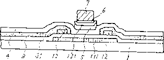
Fig. 9 shows embodiments of the invention 5 to Figure 11.Fig. 9 is the partial plan layout of the used tft array of display device of the present invention.Figure 10 is the A-A sectional drawing of Fig. 9.Figure 11 is the B-B sectional drawing of Fig. 9.At first, on the glass substrate 1 that had cleaned, form the film of the refractory metal of Cr, Ta, Ti, W, Mo, Al etc. with the method for sputtering method and so on, make its thickness become about 300nm, and form figure with the method for photoetching process etc., to form gate electrode (and grid wiring) 2, again on the position that can connect with the bridging of repairing figure as point defect that below will form formation as the figure 12 on island.Secondly, the nesa coating with methods such as sputter formation ITO (indium tin oxide) or the like makes its thickness be about 100nm.Method with photoetching process etc. makes this film form figure to form pixel capacitors 3 again.Secondly using plasma CVD (chemical vapour deposition) method etc. to form respectively will be as the SiN or the SiO of gate insulator 4
2Deng dielectric film (the about 300nm of thickness), as (the about 100nm of thickness) such as the i-a-Si of semiconductor layer 5 or polysilicons and as (the about 500nm of thickness) such as n-a-Si of ohmic contact layer 6.Secondly, the method with photoetching etc. forms wire (perhaps island) figure with n-a-Si and i-a-Si.
Method with photoetching process etc. forms figure again, forms contact hole 91 in the pixel capacitors top.Secondly with the method for sputtering method etc. form the about 400nm of thickness Al, Cr etc. metallic film and form figure with the method for photoetching process etc., to form source electrode (and source wiring) 7, drain electrode 8 and as the bridge 13 of point defect reparation figure.Next degrades the n-a-Si that is between source electrode and the drain electrode.At last, as required with formation diaphragms such as SiN.
At the tft array that makes like this and having used in its liquid crystal indicator, to being identified as the pixel of point defect, with laser the transistor that is contained in this pixel is cut off at the C-C of Fig. 9 line place earlier, then to the D on pixel capacitors part (in the part of bridge 13, in the part that has disposed island 12 in the lower floor of bridge) make the gate insulating film fusion with identical D part irradiating laser on the pixel capacitors of adjoining pixel, repair the bridge of figure by intervening acts, make the pixel capacitors of the above-mentioned pixel that is identified as point defect and the pixel capacitors short circuit of the pixel that adjoins.
Embodiments of the invention 6 are shown in Figure 12.The structure of Figure 12 is identical with the structure of embodiment 5, and the manufacturing process of different is gate electrode 2 and pixel capacitors 3 changes.Promptly form island electrode 12 in the top of pixel capacitors 3.
Figure 13 shows embodiments of the invention 7 to Figure 15.Figure 13 is the partial plan layout of tft array used in the display device of the present invention, the A-A sectional drawing that Figure 14 is Figure 13.Figure 15 is the B-B sectional drawing of Figure 13.At first, on the glass substrate 1 that cleaned, form the film of the refractory metal of Cr, Ta, Ti, W, Mo, Al or the like with methods such as sputtering methods, make its thickness be about 300nm, and form figure to form gate electrode (and grid wiring) 2 with methods such as photoetching processes, again can with position that the following bridge of repairing figure as point defect that will form is connected on form figure 12 as the island.Secondly, form the nesa coating of ITO (indium tin oxide) etc., make its thickness be about 100nm with methods such as sputtering methods.In order to obtain to surpass 150nm as the required briliancy of liquid crystal indicator, this film maximum.Make this film form figure with methods such as photoetching processes to form pixel capacitors 3.Secondly form SiN or SiO respectively with plasma CVD (chemical vapour deposition) method etc. as gate insulating film 4
2Deng dielectric film (the about 300nm of thickness), as the i-a-Si of semiconductor layer 5 or polysilicon or the like (the about 100nm of thickness) and as the SiN or the SiO of etching barrier film 101
2And so on dielectric film (the about 200nm of thickness).Secondly, with methods such as photoetching processes the etching barrier film is formed figure.
Again with formation such as plasma CVD methods as (the about 50nm of thickness) such as n-a-Si of ohmic contact layer, treat that with photoetching process method forms figure again, on pixel capacitors, form contact hole 91.Secondly, form the metallic film of Al, the Cr etc. of the about 400nm of thickness, make it to form figure to form source electrode (and source wiring) 7, drain electrode 8 and to repair figure formation bridge 13 as point defect with methods such as photoetching processes with methods such as sputtering methods.Secondly, degrade the n-a-Si that is present between source electrode and the drain electrode and be present in pixel parts do not need n-a-Si and i-a-Si.At last, as required with formation diaphragms such as SiN.
At the tft array that makes in this wise and having used in the liquid crystal indicator of this array, for the pixel that is identified as point defect, with laser the transistor that contains in this pixel is partly cut off at the C-C of Figure 13 line earlier, afterwards, D on pixel capacitors part (lower floor of the inherent bridge of the part of bridge 13 disposes the part on island 12) is made the gate insulating film fusion with identical D part irradiating laser on the pixel capacitors of adjoining pixel, by the bridge of intervening acts reparation figure, make the above-mentioned pixel capacitors and the pixel capacitors short circuit of adjoining pixel that is identified as the pixel of point defect.
Embodiments of the invention 8 are shown in Figure 16.The structure of Figure 16 is identical with the structure of embodiment 7, and different is that gate electrode 2 is changed with the order of the manufacturing process of pixel capacitors 3.Promptly form island electrode 12 in the top of pixel capacitors 3.
If employing the present invention is owing to can easily repair point defect, so can improve tft array and use the fabrication yield of its liquid crystal indicator.In addition, if employing the present invention, the point defect that the tft array stage in manufacture process is found certainly needless to say, even if for finishing the point defect of finding after the liquid crystal indicator, promptly when repairing, must make laser under the situation of pixel capacitors one side incident, also can repair easily and reliably.
In addition, it is identical that manufacturing process and existing method are finished, and only figure changes to some extent, so need not to increase operation, cost can not uprise yet.
Embodiments of the invention 9 are shown in Figure 17.Figure 17 is the partial plan layout of tft array used in the display device of the present invention.Figure 18 is the A-A sectional drawing of Figure 17.Figure 19 is the sectional drawing of the B-B of Figure 18.In the drawings, the 111st, the point defect of conduct the 1st metallic pattern that forms simultaneously with storage capacitor electrode 21 usefulness identical materials is repaired figure, the 121st, use the island of conduct the 2nd metallic pattern that forms simultaneously with gate electrode and grid wiring 2 identical materials, island 12 is connected in the bottom of pixel capacitors 3.The position of laser radiation when C-C and D are the point defect reparation among the figure.
Then, the manufacture method to the tft array in the present embodiment describes.At first, on the glass substrate 1 that cleaned, the metallic film with the formation of methods such as sputtering method Cr, Ta, Ti etc. makes it to form figure with methods such as photoetching processes, repairs figure 111 to form storage capacitor electrode 21 and point defect.Secondly, with SiN or the SiO of formation such as plasma CVD (chemical vapour deposition) method as the dielectric film 31 of memory capacitance
2Deng film, with the figure of the contact hole that is formed for contacting with grid wiring 2 with the following gate electrode that will form.Secondly, with methods such as sputtering methods, form the high melting point metal film of Cr, Ta, the Ti etc. of the about 300nm of thickness, and make it to form figure to form gate electrode and grid wiring 2 and to repair formation island 12 on the part that figure is connected with point defect with methods such as photoetching processes.That is, repair figure 111 tops in point defect and form island 12 by the dielectric 3 of getting involved memory capacitance at the D place, laser radiation position when repairing point defect.
Form the nesa coating of the ITO (indium tin oxide) etc. of the about 100nm of thickness again with methods such as sputtering methods, make it to form figure with methods such as photoetching processes then, with formation pixel capacitors 3.Then, with methods such as plasma CVD (chemical vapour deposition) methods, form SiN or SiO as the about 300nm of thickness of gate insulating film 4
2Deng dielectric film, as the i-a-Si of the about 200nm of thickness of semiconductor layer 5 or polysilicon etc., and as n-a-Si of the about 50nm of thickness of ohmic contact layer 6 etc.Secondly, with methods such as photoetching processes, make n-a-Si and i-a-Si form the figure of island or wire.Secondly, form figure, to form contact hole in pixel capacitors 3 tops with methods such as photoetching processes.Secondly, form the metallic film of Al, the Cr etc. of the about 400nm of thickness, and make it to form figure, after having formed source electrode and source wiring 7 and drain electrode 8, degrade the n-a-Si that is present between the leakage of source with methods such as photoetching processes with methods such as sputtering methods.At last, as required, with formation diaphragms such as SiN.
At the above-mentioned tft array that makes like this and having used in the liquid crystal indicator of this array, for the pixel that is identified as point defect, with laser the transistor part of this pixel is partly cut off at C-C line shown in Figure 1 earlier, afterwards, to the D on the pixel capacitors 3 part with adjoin D part irradiating laser on the pixel capacitors 3 of pixel, repair figure 111 by point defect and make the pixel capacitors short circuit of adjoining pixel.At this moment, middle two metal films having got involved the dielectric 31 of memory capacitance, i.e. point defect reparation figure 111 makes it to be connected with island 12 usefulness laser, promptly can repair easily and reliably.Be effective particularly to the laser radiation that comes from pixel capacitors 3 one sides.In addition, in the present embodiment, its formation is that the pixel capacitors about making connects, but pixel capacitors is up and down connected.
If the employing present embodiment then utilizes point defect to repair figure 111 by employing and makes the pixel that is identified as point defect and the way of neighboring pixels short circuit, it is identical that the current potential of neighboring pixels electrode is become each other, carries out identical demonstration.So no longer be easy to find out to be point defect, thereby improved the yield rate of tft array.In addition, owing to be manufacture method same as the prior art, only be that figure has changed, can not uprise the advantage that process number need not to increase so have cost.
In addition, if employing the present invention, then the point defect of being found in the tft array stage is self-evident, even if formed this tft array substrate and have transparency electrode and colored filter etc. accompany the liquid crystal indicator of liquid crystal between the electrode base board in opposite directions after, promptly under the situation of pixel capacitors one side incident laser, also can repair easily and reliably.
The local section of Figure 20 illustrates tft array used in the display device of embodiments of the invention 10.Present embodiment 10 is except the order of the manufacturing process of gate electrode and grid wiring 2 and pixel capacitors 3 has been changed, and its structure is identical with embodiment's 9.That is, the top of repairing figure 111 in point defect forms pixel capacitors 3 by the dielectric 31 of getting involved memory capacitance, forms island 12 more above that.So, island 12 no matter be any structure, can utilize point defect to repair figure 111 and easily repair point defect in the top of pixel capacitors 3 or following all right, can obtain the effect identical with embodiment 9.
With reference to description of drawings embodiments of the invention 11.Figure 21 is the partial plan layout of tft array used in the liquid crystal indicator of the present invention.Figure 22 is the A-A sectional drawing of Figure 21.Figure 23 is the B-B sectional drawing of Figure 21.Among the figure, the 131st, the etching barrier film.
Manufacture method to the tft array in the present embodiment describes.At first, on the glass substrate 1 that cleaned, form the metallic film of Cr, Ta, Ti etc., then, make it to form figure,, form point defect again and repair figure 111 to form storage capacitor electrode 21 with methods such as photoetching processes with methods such as sputtering methods.Secondly, with SiN or the SiO of plasma CVD (chemical vapour deposition) method formation as the dielectric film 31 of memory capacitance
2Deng film, make the contact hole that contacts with following gate electrode that will form and grid wiring form figure.Secondly, form the high melting point metal film of Cr, Ta, the Ti etc. of the about 300nm of thickness with methods such as sputtering methods, make it to form figure with methods such as photoetching processes again,, repairing formation island 12 on figure 111 coupling parts with point defect again to form gate electrode and grid wiring 2.Promptly figure 111 tops are repaired in point defect in the position of laser radiation when repairing point defect, form island 12 by the dielectric 31 of getting involved memory capacitance.
Form the nesa coating of the ITO (indium tin oxide) etc. of the about 100nm of thickness again with methods such as sputters.For will obtaining as the desired briliancy of liquid crystal indicator, above-mentioned thickness maximum is no more than 150nm.Make this film form figure with methods such as photoetching processes, to form pixel capacitors 3.Secondly, with SiN or the SiO of formation such as plasma CVD method as the about 300nm of thickness of gate insulating film 4
2Deng dielectric film, as the i-a-Si of the about 100nm of thickness of semiconductor layer 5 or polysilicon etc. and as SiN or the SiO of the about 200nm of thickness of etching barrier film 131
2Deng dielectric film.Secondly, with methods such as photoetching processes, make etching barrier film 131 form figure.Next, with plasma CVD method etc. form the about 50nm of thickness as the n-a-Si of ohmic contact layer 6 etc., and, form figure, with at pixel capacitors 3 tops formation contact hole with methods such as photoetching processes.Secondly, with methods such as sputtering methods, form the metallic film of Al, the Cr etc. of the about 400nm of thickness, and make it to form figure, to form source electrode and source wiring 7 and drain electrode 8 with methods such as photoetching processes.Secondly, degrade the n-a-Si that is present between the leakage of source and the n-a-Si that does not want and the i-a-Si that are present in the pixel parts.At last as required, with formation diaphragms such as SiN.
At the above-mentioned tft array that makes like this and having used in the liquid crystal indicator of this array, to being identified as the pixel of point defect, with laser the transistor part of this pixel is cut off on the C-C of Figure 21 line part earlier, then, D on the pixel capacitors 3 of the D on the pixel capacitors 3 part and adjacent image point part respectively according to laser, and is made the pixel capacitors short circuit of adjacent image point by point defect reparation figure 111.
Even if in the tft array of above-mentioned this structure, also can obtain the efficient identical with embodiment 9 and embodiment 10.
The local section of Figure 24 illustrates tft array used in the liquid crystal indicator of embodiments of the invention 12.Present embodiment 12 is except having changed the gate electrode 2 and the order of the manufacturing process of pixel capacitors 3, and its structure is identical with embodiment 11.Promptly repair the top of figure 111 earlier in point defect, form pixel capacitors 3, form island 12 then above that by the dielectric 31 of getting involved memory capacitance.Even if such structure, also utilisation point defect repair figure 111 is easily repaired point defect.Can obtain the effect identical with embodiment 9~11.
In addition, the tft array structure shown in is only sub for example in the above-described embodiments, the invention is not restricted to these structures.
As mentioned above, if employing the present invention, then make the 1st metallic pattern that on two adjacent pixels, repeats and the way of the 2nd metallic pattern fusion that forms in above-mentioned the 1st metallic pattern top by the dielectric film of getting involved memory capacitance dielectric etc. by adopting with laser radiation, just can obtain can be easily and repair the tft array substrate of picture element defect reliably and use the liquid crystal indicator of this array base palte, has the effect that improves yield rate.
In addition, if adopt manufacture method of the present invention, then owing to make the 1st metallic pattern and storage capacitor electrode and the 2nd metallic pattern and grid wiring side by side formed with identical materials respectively, its process number is identical with the process number of prior art, only change mask and get final product, thereby can easily make and cost is uprised.
Claims (20)
1. thin-film transistor array base-plate is characterized in that:
Possessing has: on transparent insulation substrate, form and have both the grid wiring that gate electrode is arranged by what metallic film constituted; By get involved the semiconductor layer that gate insulating film is provided with on this grid wiring; Constitute having both of semiconductor devices with this semiconductor layer the source wiring and the drain electrode of source electrode arranged; The pixel capacitors that constitutes by the nesa coating that closely is close to of being located at above-mentioned semiconductor device; Constitute and be configured to the 1st metallic pattern on two adjacent pixels by the metal material identical with above-mentioned grid wiring; In the top of above-mentioned the 1st metallic pattern by getting involved the 2nd metallic pattern of using the metal material identical to constitute that above-mentioned gate insulating film disposes with the source wiring drain electrode;
Make above-mentioned the 1st metallic pattern and above-mentioned the 2nd metallic pattern fusion and the way that couples together couples together two adjacent pixel capacitors to repair picture element defect with laser radiation.
2. the described thin-film transistor array base-plate of claim 1 is characterized in that grid wiring and the 1st metallic pattern are made of the metal of Cr, Ta or Ti etc.
3. the described thin-film transistor array base-plate of claim 1 is characterized in that the 2nd metallic pattern is made of the metal of Al, Cr or Mo etc.
4. the described thin-film transistor array base-plate of claim 1 is characterized in that the 2nd metallic pattern is formed top or the bottom that is connected in pixel capacitors.
5. the manufacture method of a thin-film transistor array base-plate is characterized in that comprising following operation:
Form the metallic film of Cr, Ta, Ti etc. in the transparent insulation substrate top with methods such as sputtering methods, make it to form the operation of figure with methods such as photoetching processes again to form gate electrode and grid wiring and to form the 1st metallic pattern on adjacent two pixels;
Form gate insulating film, semiconductor layer and ohmic contact layer in turn and make them form the operation of figure with methods such as plasma chemical vapor deposition methods;
Form nesa coating and form figure with methods such as sputters, to form the operation of pixel capacitors;
With the metallic film of formation Al, Cr such as sputtering method or Mo etc. and form figure, forming source electrode and source wiring and drain electrode, and in above-mentioned the 1st metallic pattern top at least by getting involved the operation that above-mentioned gate insulating film forms the 2nd metallic pattern;
When finding picture element defect, cut off the signal circuit of this pixel with laser radiation, above-mentioned the 1st metallic pattern of fusion and the 2nd metallic pattern make between two adjacent pixel capacitors to couple together again, to repair the operation of picture element defect.
6. thin-film transistor array base-plate is characterized in that:
Possessing has: have both the grid wiring that gate electrode is arranged by what the metallic film that forms on transparent insulation substrate constituted; By get involved the semiconductor layer that gate insulating film is provided with on this grid wiring; Constitute having both of semiconductor devices with this semiconductor layer the source wiring and the drain electrode of source electrode arranged; By being located at the pixel capacitors that nesa coating that above-mentioned semiconductor device closely is close to constitutes; The storage capacitor electrode that constitutes by the metallic film that is formed on the above-mentioned transparent insulation substrate; Be located at the memory capacitance dielectric film of this storage capacitor electrode top; Constitute and be set up with the metal material identical across the 1st metallic pattern between locational adjacent two pixel capacitors of isolating from above-mentioned storage capacitor electrode with above-mentioned storage capacitor electrode; Feed the dielectric film of getting involved above-mentioned memory capacitance dielectric film etc. in the top of the 1st metallic pattern and the 2nd metallic pattern that disposes;
Thereby make above-mentioned the 1st metallic pattern and above-mentioned the 2nd metallic pattern fusion and connect coupling together between two adjacent pixel capacitors to repair picture element defect with laser radiation.
7. the described thin-film transistor array base-plate of claim 6 is characterized in that storage capacitor electrode and the 1st metallic pattern are made of the metal of Cr, Ta or Ti etc.
8. the described thin-film transistor array base-plate of claim 6 is characterized in that the 2nd metallic pattern is made of the metal of Cr, Ta or Ti etc.
9. the described thin-film transistor array base-plate of claim 6 is characterized in that the 2nd metallic pattern metal material formation identical with grid wiring.
10. the described thin-film transistor array base-plate of claim 6 is characterized in that the 2nd metallic pattern is formed top or the bottom that is connected in pixel capacitors.
11. a liquid crystal indicator, it is characterized in that the described thin-film transistor array base-plate of any one claim of claim 1~4, claim 6~10 and have transparency electrode and colored filter etc. dispose liquid crystal in opposite directions between the electrode base board.
12. the manufacture method of a thin-film transistor array base-plate is characterized in that having following operation:
Form the metallic film of Cr, Ta or Ti etc. in the transparent insulation substrate top with sputtering method etc., make it to form figure with methods such as photoetching processes then, forming storage capacitor electrode, and the operation that forms the 1st metallic pattern on two adjacent pixels;
With formation SiN, SiO such as plasma chemical vapor deposition methods
2Deng, make it to form figure, to form the operation of memory capacitance dielectric film;
Form the metallic film of Cr, Ta or Ti etc. with sputtering method etc., make it to form figure with methods such as photoetching processes then, forming gate electrode and grid wiring, and get involved the operation that above-mentioned memory capacitance dielectric film forms the 2nd metallic pattern at least in above-mentioned the 1st metallic pattern top;
Method with sputter etc. forms nesa coating and forms figure, to form the operation of pixel capacitors;
Form gate insulating film, semiconductor layer and ohmic contact layer in turn with plasma chemical vapor deposition method etc., and make it to form the operation of figure;
With the metallic film of formation Al, Cr etc. such as sputtering method and make it to form figure to form the operation of source electrode and source wiring and drain electrode;
Under the situation that identifies picture element defect, cut off the signal circuit of this pixel earlier with laser radiation,, two adjacent pixel capacitors are coupled together to repair the operation of picture element defect again above-mentioned the 1st metallic pattern and the 2nd metallic pattern fusion.
13. liquid crystal indicator, this device is a kind ofly liquid crystal to be clipped in that transparent insulation substrate is provided with thin film transistor (TFT) and the thin-film transistor array base-plate of the pixel capacitors that is made of nesa coating and have transparency electrode and the liquid crystal indicator between the electrode base board in opposite directions of colored filter, above-mentioned thin film transistor (TFT) has gate electrode and the grid wiring that is made of metallic film, gate insulating film, semiconductor layer, ohmic contact layer, source electrode and source wiring and drain electrode, it is characterized in that, be formed on above the above-mentioned gate insulating film, cross-over connection neighboring pixels electrode and the bridge that constitutes by metallic film that is provided with and below above-mentioned gate insulating film, corresponding with above-mentioned bridge, and answer and a pair of island of setting with the adjacent image point electrode pair respectively.
14. the described liquid crystal indicator of claim 13 is characterized in that above-mentioned island forms with refractory metal.
15. the described liquid crystal indicator of claim 14 is characterized in that, refractory metal is any metal among Cr, Ta, W, Mo or the Al.
16. claim 13,14 or 15 described liquid crystal indicators is characterized in that the island is connected with pixel capacitors.
17. the manufacture method of a liquid crystal indicator, this method is the manufacture method of the described liquid crystal indicator of a kind of claim 13, it is characterized in that, forms the island with identical with it metal material when forming above-mentioned gate electrode and grid wiring.
18. the restorative procedure of a liquid crystal indicator, it is characterized in that: in the described liquid crystal indicator of claim 13, become the pixel capacitors that contains point defect and any one pixel capacitors work in two pixel capacitors adjacent idiostatic to repair the above-mentioned pixel capacitors that contains point defect with this pixel capacitors.
19. the restorative procedure of the described liquid crystal indicator of claim 18, it is characterized in that, the bridge of cross-over connection on any one pixel capacitors among pixel capacitors that point defect is arranged and two pixel capacitors adjacent with this pixel capacitors with and the corresponding island short circuit of this bridge so that it is idiostatic.
20. the restorative procedure of the described liquid crystal indicator of claim 19 is characterized in that, use laser make bridge and and the corresponding island of bridge between the gate insulating film fusion and form short circuit.
Applications Claiming Priority (9)
| Application Number | Priority Date | Filing Date | Title |
|---|---|---|---|
| JP131695/95 | 1995-05-30 | ||
| JP7131695A JPH08328035A (en) | 1995-05-30 | 1995-05-30 | Liquid crystal display device and its production and method for repairing spot defect |
| JP131695/1995 | 1995-05-30 | ||
| JP154863/1995 | 1995-06-21 | ||
| JP15486495A JPH095786A (en) | 1995-06-21 | 1995-06-21 | Tft array substrate as well as liquid crystal display device formed by using the tft array substrate and production of tft array substrate |
| JP154864/95 | 1995-06-21 | ||
| JP154863/95 | 1995-06-21 | ||
| JP15486395A JPH095785A (en) | 1995-06-21 | 1995-06-21 | Tft array substrate as well as liquid crystal display device formed by using the tft array substrate and production of tft array substrate |
| JP154864/1995 | 1995-06-21 |
Publications (2)
| Publication Number | Publication Date |
|---|---|
| CN1142057A CN1142057A (en) | 1997-02-05 |
| CN1105324C true CN1105324C (en) | 2003-04-09 |
Family
ID=27316352
Family Applications (1)
| Application Number | Title | Priority Date | Filing Date |
|---|---|---|---|
| CN96107917A Expired - Fee Related CN1105324C (en) | 1995-05-30 | 1996-05-30 | Array base plate, liquid-crystal displaying device of thin-film transistor, and method for production of said base plate |
Country Status (3)
| Country | Link |
|---|---|
| KR (1) | KR100363140B1 (en) |
| CN (1) | CN1105324C (en) |
| TW (1) | TW300341B (en) |
Cited By (2)
| Publication number | Priority date | Publication date | Assignee | Title |
|---|---|---|---|---|
| CN1324390C (en) * | 2004-04-28 | 2007-07-04 | 友达光电股份有限公司 | Thin film transistor array base plate and patching method thereof |
| CN101313346B (en) * | 2005-11-24 | 2011-05-04 | 夏普株式会社 | Active matrix substrate, liquid crystal panel, display, television receiver, and method of correcting and manufacturing the substrate and panel |
Families Citing this family (27)
| Publication number | Priority date | Publication date | Assignee | Title |
|---|---|---|---|---|
| KR100471391B1 (en) * | 1997-12-08 | 2005-06-07 | 비오이 하이디스 테크놀로지 주식회사 | Liquid crystal display element |
| JP3712637B2 (en) * | 2000-08-11 | 2005-11-02 | シャープ株式会社 | Liquid crystal display device and defect correcting method thereof |
| JP2002162644A (en) * | 2000-11-27 | 2002-06-07 | Hitachi Ltd | Liquid crystal display device |
| WO2004008423A1 (en) * | 2002-07-12 | 2004-01-22 | Sharp Kabushiki Kaisha | Wiring structure, display apparatus, and active device substrate |
| JP2004054069A (en) * | 2002-07-23 | 2004-02-19 | Advanced Display Inc | Display device and method for repairing disconnection of display device |
| CN100343743C (en) * | 2003-06-24 | 2007-10-17 | 统宝光电股份有限公司 | LCD laser repairing method and structure |
| CN100388460C (en) * | 2003-07-04 | 2008-05-14 | 友达光电股份有限公司 | Method for repairing thin film transistor wire on display panel |
| JP4011002B2 (en) * | 2003-09-11 | 2007-11-21 | シャープ株式会社 | Active substrate, display device and manufacturing method thereof |
| CN1324360C (en) * | 2003-10-20 | 2007-07-04 | 申丰科技有限公司 | Liquid crystal panel bright points repair treatment method uithout disassembling back light plate |
| CN1560899B (en) * | 2004-02-16 | 2010-05-05 | 友达光电股份有限公司 | Thin film transistor array substrate and its repair method |
| CN100442479C (en) * | 2004-04-28 | 2008-12-10 | 友达光电股份有限公司 | Method for repairing thin-film transistor array substrate and thin film removing method |
| CN1306332C (en) * | 2004-04-29 | 2007-03-21 | 友达光电股份有限公司 | Thin film transistor array base plate and patching method thereof |
| CN1306557C (en) * | 2004-07-27 | 2007-03-21 | 友达光电股份有限公司 | Thin film transistor array base plate and its repairing method |
| CN100341155C (en) * | 2004-11-16 | 2007-10-03 | 友达光电股份有限公司 | Picture element structure and thin film transistor array and mending method thereof |
| CN100437223C (en) * | 2005-09-30 | 2008-11-26 | 友达光电股份有限公司 | Display device, repairing structure for display device circuit and its production |
| CN100454556C (en) * | 2006-07-05 | 2009-01-21 | 友达光电股份有限公司 | Repairing structure and active component array substrate |
| KR100947273B1 (en) * | 2006-12-29 | 2010-03-11 | 엘지디스플레이 주식회사 | Array substrate for In-plane switching mode liquid crystal display device |
| KR101041618B1 (en) | 2008-04-24 | 2011-06-15 | 엘지디스플레이 주식회사 | Array substrate for LCD device and method of fabricating the same |
| CN101285977B (en) * | 2008-05-30 | 2010-06-02 | 昆山龙腾光电有限公司 | LCD device and its array substrate |
| CN101614916B (en) | 2008-06-25 | 2012-05-30 | 北京京东方光电科技有限公司 | TFT-LCD pixel structure and method for restoring broken line of liquid crystal display |
| CN103149755B (en) * | 2011-12-06 | 2015-09-16 | 上海中航光电子有限公司 | A kind of thin-film transistor LCD device and restorative procedure thereof |
| CN102736341B (en) * | 2012-07-10 | 2015-08-19 | 深圳市华星光电技术有限公司 | A kind of display panels and restorative procedure thereof |
| CN105654886A (en) * | 2016-01-25 | 2016-06-08 | 重庆京东方光电科技有限公司 | Grid drive circuit, repairing method thereof and display device |
| KR20180052166A (en) * | 2016-11-09 | 2018-05-18 | 엘지디스플레이 주식회사 | Photo sensor and display device having the same |
| CN107515500A (en) * | 2017-09-20 | 2017-12-26 | 深圳市华星光电技术有限公司 | Array base palte, display panel and pixel method for repairing and mending |
| US11735600B2 (en) | 2020-05-19 | 2023-08-22 | Shenzhen China Star Optoelectronics Semiconductor Display Technology Co., Ltd. | Pixel layout and display panel having pixel layout |
| CN111627925B (en) * | 2020-05-19 | 2023-10-13 | 深圳市华星光电半导体显示技术有限公司 | Pixel layout and display panel with same |
Family Cites Families (4)
| Publication number | Priority date | Publication date | Assignee | Title |
|---|---|---|---|---|
| JPH0786619B2 (en) * | 1989-04-26 | 1995-09-20 | シャープ株式会社 | Active matrix display |
| JPH0421823A (en) * | 1990-05-16 | 1992-01-24 | Hosiden Corp | Method for making spot defect of liquid crystal display element into block defect and liquid crystal display element |
| JPH04261521A (en) * | 1991-01-21 | 1992-09-17 | Mitsubishi Electric Corp | Liquid crystal display device and method for repairing display defect thereof |
| JP2801104B2 (en) * | 1992-01-29 | 1998-09-21 | シャープ株式会社 | Manufacturing method of active matrix drive type scattering type liquid crystal display device |
-
1996
- 1996-05-21 TW TW085105967A patent/TW300341B/zh active
- 1996-05-30 CN CN96107917A patent/CN1105324C/en not_active Expired - Fee Related
- 1996-05-30 KR KR1019960018811A patent/KR100363140B1/en not_active IP Right Cessation
Cited By (2)
| Publication number | Priority date | Publication date | Assignee | Title |
|---|---|---|---|---|
| CN1324390C (en) * | 2004-04-28 | 2007-07-04 | 友达光电股份有限公司 | Thin film transistor array base plate and patching method thereof |
| CN101313346B (en) * | 2005-11-24 | 2011-05-04 | 夏普株式会社 | Active matrix substrate, liquid crystal panel, display, television receiver, and method of correcting and manufacturing the substrate and panel |
Also Published As
| Publication number | Publication date |
|---|---|
| TW300341B (en) | 1997-03-11 |
| CN1142057A (en) | 1997-02-05 |
| KR960042181A (en) | 1996-12-21 |
| KR100363140B1 (en) | 2003-08-14 |
Similar Documents
| Publication | Publication Date | Title |
|---|---|---|
| CN1105324C (en) | Array base plate, liquid-crystal displaying device of thin-film transistor, and method for production of said base plate | |
| CN1163964C (en) | Film transistor array panel for liquid crystal display device | |
| CN1258114C (en) | Liquid crystal display and its making method | |
| CN1288477C (en) | Array substrate for liquid crystal display device and producing method thereof | |
| CN1324387C (en) | Array baseboard of LCD and its producing method | |
| CN1313876C (en) | Method for manufacturing dot structure of thin film transistor liquid crystal display | |
| KR100264112B1 (en) | Active matrix panel and manufacturing method of the same | |
| CN100454561C (en) | Film transistor array substrates and its producing method, repairing method | |
| CN1773354A (en) | Liquid crystal display device and method of fabricating the same | |
| CN1648756A (en) | Active matrix substrate and display device | |
| CN1716062A (en) | Method for producing array board of liquid crystal display device | |
| CN1992291A (en) | Thin film transistor substrate and fabricating method thereof | |
| CN1819217A (en) | Active matrix substrate and its manufacturing method | |
| CN1495477A (en) | Display base plate, liquid crystal display and method for mfg. the same | |
| CN1744322A (en) | Film transistor array plate | |
| CN1280308A (en) | Film transistor array and its producing method | |
| CN1991556A (en) | Array substrate for in-plane switching mode liquid crystal display device and method of manufacturing the same | |
| US7291871B2 (en) | Pixel structure | |
| CN1375733A (en) | Liquid crystal display device having bimetallic layer source electrode and drain electrode and its manufacturing method | |
| TWI392096B (en) | Thin film transistor array panel | |
| EP0315319A2 (en) | Liquid crystal display device | |
| CN1862320A (en) | Method of repairing disconnection, method of manufacturing active matrix substrate by using thereof, and display device | |
| US7026648B2 (en) | Pixel structure | |
| CN1255701C (en) | Active matrix crystal display devices and manufacturing methods thereof | |
| CN1585088A (en) | Producing method for thin-film transistor array baseplate |
Legal Events
| Date | Code | Title | Description |
|---|---|---|---|
| C06 | Publication | ||
| PB01 | Publication | ||
| C10 | Entry into substantive examination | ||
| SE01 | Entry into force of request for substantive examination | ||
| C14 | Grant of patent or utility model | ||
| GR01 | Patent grant | ||
| ASS | Succession or assignment of patent right |
Owner name: MITSUBISHI ELECTRIC CO., LTD. Free format text: FORMER OWNER: CO., LTD. ADVANCED DISPLAY Effective date: 20080104 |
|
| C41 | Transfer of patent application or patent right or utility model | ||
| TR01 | Transfer of patent right |
Effective date of registration: 20080104 Address after: Tokyo, Japan, Japan Patentee after: Missubishi Electric Co., Ltd. Address before: Xiongben Prefecture, Japan Patentee before: Advanced Display Inc. |
|
| C17 | Cessation of patent right | ||
| CF01 | Termination of patent right due to non-payment of annual fee |
Granted publication date: 20030409 |