CN110087809B - Pad conditioner with pad and wafer planarization system - Google Patents
Pad conditioner with pad and wafer planarization system Download PDFInfo
- Publication number
- CN110087809B CN110087809B CN201780078805.XA CN201780078805A CN110087809B CN 110087809 B CN110087809 B CN 110087809B CN 201780078805 A CN201780078805 A CN 201780078805A CN 110087809 B CN110087809 B CN 110087809B
- Authority
- CN
- China
- Prior art keywords
- carrier
- pad
- pad conditioner
- abrasive
- conditioner
- Prior art date
- Legal status (The legal status is an assumption and is not a legal conclusion. Google has not performed a legal analysis and makes no representation as to the accuracy of the status listed.)
- Active
Links
Images


Classifications
-
- B—PERFORMING OPERATIONS; TRANSPORTING
- B24—GRINDING; POLISHING
- B24B—MACHINES, DEVICES, OR PROCESSES FOR GRINDING OR POLISHING; DRESSING OR CONDITIONING OF ABRADING SURFACES; FEEDING OF GRINDING, POLISHING, OR LAPPING AGENTS
- B24B53/00—Devices or means for dressing or conditioning abrasive surfaces
- B24B53/017—Devices or means for dressing, cleaning or otherwise conditioning lapping tools
-
- B—PERFORMING OPERATIONS; TRANSPORTING
- B24—GRINDING; POLISHING
- B24B—MACHINES, DEVICES, OR PROCESSES FOR GRINDING OR POLISHING; DRESSING OR CONDITIONING OF ABRADING SURFACES; FEEDING OF GRINDING, POLISHING, OR LAPPING AGENTS
- B24B1/00—Processes of grinding or polishing; Use of auxiliary equipment in connection with such processes
-
- B—PERFORMING OPERATIONS; TRANSPORTING
- B24—GRINDING; POLISHING
- B24B—MACHINES, DEVICES, OR PROCESSES FOR GRINDING OR POLISHING; DRESSING OR CONDITIONING OF ABRADING SURFACES; FEEDING OF GRINDING, POLISHING, OR LAPPING AGENTS
- B24B21/00—Machines or devices using grinding or polishing belts; Accessories therefor
- B24B21/02—Machines or devices using grinding or polishing belts; Accessories therefor for grinding rotationally symmetrical surfaces
-
- B—PERFORMING OPERATIONS; TRANSPORTING
- B24—GRINDING; POLISHING
- B24B—MACHINES, DEVICES, OR PROCESSES FOR GRINDING OR POLISHING; DRESSING OR CONDITIONING OF ABRADING SURFACES; FEEDING OF GRINDING, POLISHING, OR LAPPING AGENTS
- B24B37/00—Lapping machines or devices; Accessories
- B24B37/04—Lapping machines or devices; Accessories designed for working plane surfaces
-
- B—PERFORMING OPERATIONS; TRANSPORTING
- B24—GRINDING; POLISHING
- B24B—MACHINES, DEVICES, OR PROCESSES FOR GRINDING OR POLISHING; DRESSING OR CONDITIONING OF ABRADING SURFACES; FEEDING OF GRINDING, POLISHING, OR LAPPING AGENTS
- B24B37/00—Lapping machines or devices; Accessories
- B24B37/11—Lapping tools
- B24B37/12—Lapping plates for working plane surfaces
- B24B37/16—Lapping plates for working plane surfaces characterised by the shape of the lapping plate surface, e.g. grooved
-
- B—PERFORMING OPERATIONS; TRANSPORTING
- B24—GRINDING; POLISHING
- B24B—MACHINES, DEVICES, OR PROCESSES FOR GRINDING OR POLISHING; DRESSING OR CONDITIONING OF ABRADING SURFACES; FEEDING OF GRINDING, POLISHING, OR LAPPING AGENTS
- B24B37/00—Lapping machines or devices; Accessories
- B24B37/11—Lapping tools
- B24B37/20—Lapping pads for working plane surfaces
- B24B37/24—Lapping pads for working plane surfaces characterised by the composition or properties of the pad materials
- B24B37/245—Pads with fixed abrasives
-
- B—PERFORMING OPERATIONS; TRANSPORTING
- B24—GRINDING; POLISHING
- B24B—MACHINES, DEVICES, OR PROCESSES FOR GRINDING OR POLISHING; DRESSING OR CONDITIONING OF ABRADING SURFACES; FEEDING OF GRINDING, POLISHING, OR LAPPING AGENTS
- B24B37/00—Lapping machines or devices; Accessories
- B24B37/11—Lapping tools
- B24B37/20—Lapping pads for working plane surfaces
- B24B37/26—Lapping pads for working plane surfaces characterised by the shape of the lapping pad surface, e.g. grooved
-
- B—PERFORMING OPERATIONS; TRANSPORTING
- B24—GRINDING; POLISHING
- B24B—MACHINES, DEVICES, OR PROCESSES FOR GRINDING OR POLISHING; DRESSING OR CONDITIONING OF ABRADING SURFACES; FEEDING OF GRINDING, POLISHING, OR LAPPING AGENTS
- B24B37/00—Lapping machines or devices; Accessories
- B24B37/34—Accessories
-
- B—PERFORMING OPERATIONS; TRANSPORTING
- B24—GRINDING; POLISHING
- B24D—TOOLS FOR GRINDING, BUFFING OR SHARPENING
- B24D18/00—Manufacture of grinding tools or other grinding devices, e.g. wheels, not otherwise provided for
- B24D18/0009—Manufacture of grinding tools or other grinding devices, e.g. wheels, not otherwise provided for using moulds or presses
-
- B—PERFORMING OPERATIONS; TRANSPORTING
- B24—GRINDING; POLISHING
- B24D—TOOLS FOR GRINDING, BUFFING OR SHARPENING
- B24D3/00—Physical features of abrasive bodies, or sheets, e.g. abrasive surfaces of special nature; Abrasive bodies or sheets characterised by their constituents
-
- B—PERFORMING OPERATIONS; TRANSPORTING
- B24—GRINDING; POLISHING
- B24D—TOOLS FOR GRINDING, BUFFING OR SHARPENING
- B24D3/00—Physical features of abrasive bodies, or sheets, e.g. abrasive surfaces of special nature; Abrasive bodies or sheets characterised by their constituents
- B24D3/02—Physical features of abrasive bodies, or sheets, e.g. abrasive surfaces of special nature; Abrasive bodies or sheets characterised by their constituents the constituent being used as bonding agent
- B24D3/04—Physical features of abrasive bodies, or sheets, e.g. abrasive surfaces of special nature; Abrasive bodies or sheets characterised by their constituents the constituent being used as bonding agent and being essentially inorganic
- B24D3/06—Physical features of abrasive bodies, or sheets, e.g. abrasive surfaces of special nature; Abrasive bodies or sheets characterised by their constituents the constituent being used as bonding agent and being essentially inorganic metallic or mixture of metals with ceramic materials, e.g. hard metals, "cermets", cements
-
- B—PERFORMING OPERATIONS; TRANSPORTING
- B24—GRINDING; POLISHING
- B24D—TOOLS FOR GRINDING, BUFFING OR SHARPENING
- B24D7/00—Bonded abrasive wheels, or wheels with inserted abrasive blocks, designed for acting otherwise than only by their periphery, e.g. by the front face; Bushings or mountings therefor
- B24D7/06—Bonded abrasive wheels, or wheels with inserted abrasive blocks, designed for acting otherwise than only by their periphery, e.g. by the front face; Bushings or mountings therefor with inserted abrasive blocks, e.g. segmental
- B24D7/066—Grinding blocks; their mountings or supports
-
- H—ELECTRICITY
- H01—ELECTRIC ELEMENTS
- H01L—SEMICONDUCTOR DEVICES NOT COVERED BY CLASS H10
- H01L21/00—Processes or apparatus adapted for the manufacture or treatment of semiconductor or solid state devices or of parts thereof
- H01L21/02—Manufacture or treatment of semiconductor devices or of parts thereof
- H01L21/04—Manufacture or treatment of semiconductor devices or of parts thereof the devices having at least one potential-jump barrier or surface barrier, e.g. PN junction, depletion layer or carrier concentration layer
- H01L21/18—Manufacture or treatment of semiconductor devices or of parts thereof the devices having at least one potential-jump barrier or surface barrier, e.g. PN junction, depletion layer or carrier concentration layer the devices having semiconductor bodies comprising elements of Group IV of the Periodic System or AIIIBV compounds with or without impurities, e.g. doping materials
- H01L21/30—Treatment of semiconductor bodies using processes or apparatus not provided for in groups H01L21/20 - H01L21/26
- H01L21/31—Treatment of semiconductor bodies using processes or apparatus not provided for in groups H01L21/20 - H01L21/26 to form insulating layers thereon, e.g. for masking or by using photolithographic techniques; After treatment of these layers; Selection of materials for these layers
- H01L21/3205—Deposition of non-insulating-, e.g. conductive- or resistive-, layers on insulating layers; After-treatment of these layers
- H01L21/321—After treatment
- H01L21/32115—Planarisation
- H01L21/3212—Planarisation by chemical mechanical polishing [CMP]
-
- H—ELECTRICITY
- H01—ELECTRIC ELEMENTS
- H01L—SEMICONDUCTOR DEVICES NOT COVERED BY CLASS H10
- H01L21/00—Processes or apparatus adapted for the manufacture or treatment of semiconductor or solid state devices or of parts thereof
- H01L21/67—Apparatus specially adapted for handling semiconductor or electric solid state devices during manufacture or treatment thereof; Apparatus specially adapted for handling wafers during manufacture or treatment of semiconductor or electric solid state devices or components ; Apparatus not specifically provided for elsewhere
- H01L21/67005—Apparatus not specifically provided for elsewhere
- H01L21/67011—Apparatus for manufacture or treatment
- H01L21/67092—Apparatus for mechanical treatment
Abstract
The pad conditioner includes a carrier, at least one grinding element, and a pad. The carrier includes a surface having an exposed area and a plurality of mounting areas. The abrasive elements are disposed on the mounting region of the carrier, and at least one of the abrasive elements has a working surface including a plurality of features each having a distal end. The gasket is disposed on a surface of the carrier and covers at least a portion of the exposed area. The shim has a first surface and a second surface, wherein the second surface is opposite the first surface and adjacent to a surface of the carrier. A distance D1 between a distal end of a highest feature of the at least one grinding element and the surface of the carrier is greater than a distance D2 between the first surface of the shim and the surface of the carrier.
Description
Technical Field
The present invention relates to pads for pad conditioners of wafer chemical mechanical planarization systems, pad conditioners with such pads and wafer chemical mechanical planarization systems having pad conditioners with such pads.
Background
Chemical Mechanical Planarization (CMP) is a process for smoothing the surface of a wafer. To provide adequate polishing capabilities, the surface of the pad is refreshed by the pad conditioner sweeping the pad surface between the center of the pad and the edge of the pad.
Diamond disk pad conditioners are commonly used in CMP processes. However, if the diamond grit of the diamond disk is not uniformly embedded, wafer damage will result during the CMP operation. To address such problems, novel Chemical Vapor Deposition (CVD) pad modulators were developed (U.S. publication nos. US20150209932a1(Duy K lehu et al), US20150087212a1(Patrick Doering et al), US20160074993a1(Joseph Smith et al), US20160121454a1(Jun Ho Song et al), US20090224370a1(david. slot), US 20110250826a1(So Young bamboo et al), and US5921856A (Jerry w. zipper)).
Disclosure of Invention
Compared to diamond disk pad conditioners, CVD pad conditioners exhibit several advantages such as long disk life, low wafer defect rates, low pad wear rates, and high disk uniformity. However, the new pad conditioner has a smaller scanning distance on the pad surface than the diamond disk pad conditioner. In other words, the scanning distance of the new pad conditioner is limited to the number and location of the abrasive elements.
To address these problems, the present invention is directed to a pad for a CVD pad conditioner for use in a chemical mechanical planarization process. With the pad conditioner of the present invention, pad edge damage (such as roll-up) when the pad conditioner is rotated onto the pad edge can be avoided. In addition, the creation of deeper penetrations and friction near the edge of the pad due to the increased downward force of elements held on the pad as a result of portions of the pad conditioner sweeping across the diameter of the pad may be mitigated.
In one embodiment, the present invention is a pad conditioner comprising a carrier, at least one abrasive element, and a pad. The carrier includes a surface having an exposed area and a plurality of mounting areas. The abrasive element is disposed on a mounting region of a surface of the carrier, and at least one abrasive element having a working surface includes a plurality of features each having a distal end. A gasket is disposed on a surface of the carrier and covers at least a portion of the exposed area, wherein the gasket has a first surface and a second surface opposite the first surface, and the second surface is adjacent to a surface of the carrier. A distance (D1) between a distal end of a highest feature of the at least one grinding element and a surface of the carrier is greater than a distance (D2) between the first surface of the shim and the surface of the carrier.
In another embodiment, the invention is a pad disposed on a pad conditioner comprising a carrier and at least one abrasive element. The carrier of the pad conditioner includes a surface having an exposed area and a plurality of mounting areas. The abrasive element is disposed on a mounting region of the carrier surface and includes a plurality of features. The gasket includes a first surface and a second surface opposite each other, wherein the second surface is adjacent to the carrier. A distance (D1) between a distal end of a highest feature of the abrasive elements and a surface of the carrier is greater than a distance (D2) between the first surface of the shim and the surface of the carrier.
In yet another embodiment, the invention is a wafer chemical mechanical planarization system that includes a platen, a pad disposed on the platen and having an abrasive surface, and a pad conditioner. The pad conditioner includes a carrier, at least one grinding element, and a pad. The carrier includes a surface having an exposed area and a plurality of mounting areas, and the abrasive elements are disposed on the mounting areas of the surface of the carrier. At least one abrasive element includes a working surface facing the pad and includes a plurality of features each having a distal end. A gasket is disposed on a surface of the carrier and covers at least a portion of the exposed area, wherein the gasket has a first surface and a second surface opposite each other, and the second surface is adjacent the carrier surface. The distal end of the uppermost feature of the abrasive element is in contact with the abrasive surface of the pad, and there is a gap (G) between the first surface of the pad and the abrasive surface of the pad.
Drawings
Fig. 1 is a schematic diagram of a pad conditioner according to one embodiment of the present invention.
Fig. 2 is a cross-sectional view of a-a' of fig. 1.
Fig. 3 is an enlarged view of region b in fig. 2.
Figure 4 is a schematic diagram of a wafer chemical mechanical planarization system in accordance with one embodiment of the present invention.
Fig. 5 is a top view of a pad conditioner according to a second embodiment of the present invention.
Fig. 6 is a top view of a pad conditioner according to a third embodiment of the present invention.
Fig. 7 is a top view of a pad conditioner according to a fourth embodiment of the present invention.
Fig. 8 is a top view of a pad conditioner according to a fifth embodiment of the present invention.
Fig. 9 is a top view of a pad conditioner according to a sixth embodiment of the present invention.
Fig. 10 is a top view of a pad conditioner according to a seventh embodiment of the present invention.
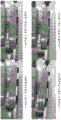
Fig. 11(a) -11 (h) show the inclinations of the disc at different positions in comparative example 1.
Fig. 12(a) -12 (h) are the inclinations of the disc at different positions in example 1.
Fig. 13 is a comparison of the inclinations of comparative example 1 and example 1.
Detailed Description
Embodiments of the present invention will be described in detail below with reference to the accompanying drawings. However, the invention should not be limited by the drawings and may be embodied in other forms. The same reference numbers will be used throughout the following description to refer to the same or like elements.
Referring now to fig. 1, a pad conditioner 1 for a Chemical Mechanical Planarization (CMP) process includes a carrier 10, at least one abrasive element 12, and a pad 14. The carrier 10 comprises a surface 101, which surface 101 comprises an exposed area 103 and a plurality of mounting areas 105. In this embodiment, the carrier 10 is circular in shape, and the mounting regions 105 are spaced at equal intervals around the circumference of the carrier 10.
The abrasive elements 12 are disposed on the mounting region 105 of the surface 101 of the carrier 10 via an adhesive, but the method for securing the abrasive elements 12 to the mounting region 105 of the carrier 10 is not limited. The abrasive elements 12 are spaced at equal intervals around the circumference of the carrier 10. In this embodiment, there are 5 abrasive elements mounted on the carrier 10, and thus the abrasive elements 12 are equally spaced 72 degrees around the circumference of the carrier 10. However, the number of grinding elements 12 is not limited, and can be adjusted to different requirements. Other embodiments may include at least one or up to 16 abrasive elements.
At least one of the abrasive elements 12 includes a working surface 121 having a plurality of features 123 formed thereon. In this embodiment, each of the abrasive elements 12 has a plurality of features 123 (fig. 2 and 3) formed on the working surface 121. Each of the features 123 has a distal end 125, and the distal end 125 of the highest feature 123 of the abrasive element 12 has a distance D1 from the surface 101 of the carrier 10. Features 123 are precisely shaped features that can be formed by methods such as machining or micromachining, water jet cutting, injection molding, extrusion, microreplication, or ceramic molding. However, the shape of the features 123 is not limited to a precise shape, and the shape of the features may be modified according to different grinding requirements. In some embodiments of the invention, the abrasive element 12 may comprise the following materials: coarse superabrasive grains in a metal matrix, a ceramic body comprising a ceramic material in an amount of at least 85% by weight, and a ceramic body comprising a diamond coating. Examples of coarse superabrasive particles are Cubic Boron Nitride (CBN) and CVD diamond. Details of the carrier 10 and the abrasive elements 12 are discussed in U.S. patent publication US20150209932a1(Duy k. lehuu et al), which is incorporated herein by reference.
In addition to the carrier 10 and the abrasive element 12, the pad conditioner 1 comprises a pad 14. The spacer 14 is disposed on the surface 101 of the carrier 10 and covers at least a portion of the exposed area 103. The gasket 14 includes the second and third mutually oppositeA surface 141 and a second surface 143, and the second surface 143 of the gasket 14 is adjacent to the surface 101 of the carrier (shown in fig. 2). The second surface 143 of the gasket 14 may be via an adhesive (such as 3M)TMVHBTMAdhesive tapes or 3MTMSCOTCH-WELDTMEpoxy adhesive, but not limited thereto) is fixed to the carrier 10. For example, the gasket may be integrated with the carrier. The coverage ratio of the pads 14 to the exposed area 103 of the surface 101 of the carrier 10 may be in the range of 1.7% to 100%.
In this embodiment, the pad 14 is 5-lobed in shape having a plurality of pockets 145 in its periphery to receive the abrasive elements 12. However, the shape of the spacer 14 is not limited. As shown in FIG. 5, the shim 24 may include a plurality of openings, and each opening may be associated with one of the abrasive elements 12. The perimeter of the pad 24 is substantially aligned with the outer edge of the carrier 10 and thus the pad 24 covers about 100% of the exposed area 103 of the surface 101 of the carrier 10.
Referring to fig. 5-8, in some other embodiments, the shims 34, 44, 54 are substantially circular or annular in shape and are concentrically disposed on the carrier within the circumference of the carrier 10. As shown in fig. 6, the spacer 34 has approximately the same dimensions as the grinding elements 12 and is disposed at the center of the carrier 10. In other words, the center of the pad 34 is aligned with the center of the carrier 10. In this embodiment, the diameter of the carrier 10 is about 107.95mm and the diameter of the grinding elements 12 is about 13.6mm, so the coverage of the pad 34 with the exposed area 103 of the carrier 10 is about 1.7%.
In some other embodiments, the gasket may be annular in shape. Referring to fig. 7, the spacer 44 has a circular ring shape and is concentrically disposed on the carrier 10 within the circumference of the carrier 10. The abrasive elements 12 are disposed within the inner edge of the pad 44 and the outer edge of the pad is located within the circumference of the carrier 10. The size of the ring is not limited, however, for example, as shown in fig. 8, the circular ring-shaped shim 54 is smaller than that of fig. 7, wherein the outer edge of the shim 54 has a diameter smaller than the diameter of the circle in which the abrasive elements are disposed.
In other embodiments, the shims 64, 74 include a plurality of ribs 641, 741. As shown in fig. 9 and 10, the gasket 64 includes a plurality of ribs 641, and each of the ribs 641, 741 is spaced at equal intervals around the circumference of the carrier 10, and one abrasive element 12 is disposed between adjacent two of the ribs 641. In other words, the ribs 641 are arranged in a radial shape. The shape of the rib is not limited, and for example, it may be a rectangular shape (as shown in fig. 9) or a triangular shape (as shown in fig. 10). In addition, the ribs 641 may be separated from each other (as shown in fig. 9) or may be in contact with each other (as shown in fig. 10).
According to these embodiments, it is understood that the coverage ratio of the spacer to the exposed area of the surface of the carrier is in the range of 1.7% to 100%. For example: 1.7%, 5.0%, 10.0%, 15.0%, 20.0%, 25.0%, 30.0%, 35.0%, 40.0%, 45.0%, 50.0%, 55.0%, 60.0%, 65.0%, 70.0%, 75.0%, 80.0%, 85.0%, 90.0%, 100.0%, or any percentage between 1.7% and 100.0%.
Referring now to fig. 2, the pad 14 further includes a beveled edge 147, and the angle a between the beveled edge 147 and the surface 101 of the carrier 10 is in the range of 10 degrees to 80 degrees. In other embodiments, angle a is in the range of 30 degrees to 60 degrees. In another embodiment, angle a is about 45 degrees. The spacer 14 has a thickness, in other words, when the spacer 14 is arranged on the surface 101 of the carrier 10, there is a distance D2 between the first surface 141 and the surface 101 of the carrier 10. The distance D2 is approximately in the range of 2.9mm to 3.5 mm. To avoid the effect of the pad 14 on the grinding ability of the grinding element 12, the distance D2 between the first surface 141 of the pad 14 and the surface 101 of the carrier 10 is less than the distance D1 between the distal ends 125 of the highest features 123 on the working surface 121 of the grinding element 12. In some embodiments, the difference between distance D1 and distance D2 is in the range of 0.2mm to 0.7 mm. For example, the difference between distance D1 and distance D2 may be 0.2mm, 0.3mm, 0.4mm, 0.5mm, 0.6mm, 0.7mm, or any value between 0.2mm and 0.7 mm.
The pad 14 may be made of a material that is durable to the various slurries used in the CMP process and that does not interact with the slurry, pad, or pad conditioner itself. For example, the material of the gasket 14 may be selected from polymers such as Polyethylene (PE), polypropylene (PP), Polystyrene (PS), poly (vinyl chloride) (PVC), Acrylonitrile Butadiene Styrene (ABS), polymethyl methacrylate (PMMA), Polyamide (PA), Polyoxymethylene (POM), poly (butylene terephthalate) (PBT), Polycarbonate (PC), poly (phenylene oxide) (PPO), polyphenylene sulfide (PPS), poly (propylene imine) (PI), Liquid Crystal Plastic (LCP), poly (tetrafluoroethylene) (PTFE), poly (ether-ketone) (PEEK), polycyclic aromatic resin (LCP), PAR (PSF), Polyethersulfone (PES), Polyetherimide (PEI), or poly (amide-imide) (PAI), phenolic resin, melamine resin, urea-formaldehyde resin (UF), Polyurethane (PU), or epoxy resin, but is not limited thereto. In other embodiments, the material of the gasket 14 may include a ceramic such as sapphire or glass. In another aspect of the invention, the gasket may be a brush material such as BRUSHLON product from 3M Company, USA. Generally, the down force at the polishing pad can be about 4-10 pounds, and can be as high as 15 pounds. Thus, the stiffness of pad 14 is preferably high enough to withstand these forces to provide a support function and avoid pad conditioner imbalance if the pad conditioner sweeps across the pad diameter.
The pad conditioner 1 with a pad may be applied in a wafer Chemical Mechanical Planarization (CMP) system. As shown in fig. 4, wafer chemical mechanical planarization system 8 includes a platen 81, a pad 82, and a pad conditioner 1. The pad 82 is disposed on the platen 80 and includes an abrasive surface 821. Pad conditioner 1 is similar to the pad conditioner of fig. 1 and will not be described in detail herein. In the wafer chemical mechanical planarization system 8, the surface 101 of the carrier 10 faces the abrasive surface 821 of the pad 82, with the surface 101 being substantially parallel to the abrasive surface 821. The features 123 of the polishing element 12 contact the polishing surface 821 of the pad 82 to condition the polishing surface 821. The first surface of the shim and the abrasive surface 821 of the pad 82 have a gap G therebetween, in some embodiments, greater than or equal to 0.2mm but not greater than 0.7 mm. For example, the gap G may be 0.2mm, 0.3mm, 0.4mm, 0.5mm, 0.6mm, 0.7mm, or any value between 0.2mm and 0.7 mm.
Referring to fig. 4, when pad conditioner 1 sweeps over the edge of pad 82, e.g., when one of grinding elements 12 exceeds the edge of the pad, pad 14 of pad conditioner 1 may support pad conditioner 1 and maintain the balance of pad conditioner 1 to mitigate tilting of pad conditioner 1 relative to pad 82. Therefore, the rocking and shaving of the edge of the pad 82 due to the oscillation can be mitigated. In addition, the beveled edges 147 of pad 14 prevent damage to the edges of pad 82 when pad conditioner 1 is swept back to the center of pad 82. The pad conditioner of the present invention is also capable of conditioning the edge of the pad such that CMP performance (e.g., material removal rate) is uniform across the wafer surface.
The invention is further described by the following examples:
examples
Comparative example 1: TRIZACT B25-2910-5S2 disks (from 3M Company, St.Paul, MN, US, St.) of St.Paul, Minn.) were placed on an AMAT REFLEXION tool (Applied Materials, Inc., Santa Clara, Calif.). This disk has no pads-this pad is a JSR CMP 9006-FPJ pad (JSR Corporation, Tokyo, JP, Tokyo, Japan). The disc was positioned near the edge of the pad (outer radial scan position) (step 1), and then the disc was lowered until it contacted with 6 pounds of downward force (step 2). A picture of the disc is taken to record the tilt (step 3). The disc is lifted off the pad and the disc position is increased outward to record the tilt (step 4). Repeat steps 3 and 4 to record the tilt.
Example 1: the pan, tools and pads were identical to those in comparative example 1, except that the pads of the present invention were attached to the pan via VHB tape (3M Company, st. paul, MN US) from 3M Company of saint paul, minnesota. The gasket is a 5-lobe gasket made of PMMA. The shim has a thickness of 3mm and a chord length of 47.2mm per arc. Step 3 and step 4 described in comparative example 1 above were repeated to record the tilt.
The results are shown in fig. 11 to 13. Some tilting is evident in the comparative example without shims when the disc extends to the point where at least one element is not supported by the pad (fig. 11(f) -fig. 11 (h)). With the shim, the amount of tilt is significantly reduced (fig. 12 and 13).
Although the present invention has been described in detail with reference to certain embodiments thereof, other versions are possible. Therefore, the spirit and scope of the appended claims should not be limited to the description and drawings set forth herein. It is also to be understood that the terminology used in the description is for the purpose of describing the particular versions or embodiments only, and is not intended to limit the scope of the present invention.
Claims (26)
1. A pad conditioner, comprising:
a carrier comprising a surface having an exposed area and a plurality of mounting areas;
at least one abrasive element disposed on a mounting region of a surface of the carrier, the at least one abrasive element having a working surface comprising a plurality of features each having a distal end; and
a shim disposed on the surface of the carrier and covering at least a portion of the exposed area, wherein the shim has a first surface and a second surface opposite the first surface, the second surface being adjacent the surface of the carrier, and the shim further includes a beveled edge, and an angle (A) between the beveled edge and the surface of the carrier is 10 to 80 degrees;
wherein a distance (D1) between a distal end of a highest feature of the at least one grinding element and the surface of the carrier is greater than a distance (D2) between a first surface of the shim and the surface of the carrier.
2. The pad conditioner of claim 1, wherein said at least one grinding element comprises one or more of: coarse superabrasive grains in a metal matrix, a ceramic body comprising a ceramic material in an amount of at least 85% by weight, and a ceramic body comprising a diamond coating.
3. The pad conditioner of claim 1, wherein the plurality of features of said abrasive element are precisely shaped features.
4. The pad conditioner of claim 1, wherein said abrasive elements are spaced at equal intervals around the circumference of said carrier.
5. The pad conditioner of claim 4, wherein said abrasive elements are equally spaced 72 degrees around the circumference of said carrier.
6. The pad conditioner of claim 1 wherein the coverage ratio of said spacer to the exposed area of the surface of said carrier is 1.7% to 100%.
7. The pad conditioner of claim 5, wherein said spacer is concentrically disposed within the circumference of said carrier.
8. The pad conditioner of claim 5 wherein the gasket further includes a plurality of ribs and each of the ribs are spaced at equal intervals around the circumference of the carrier.
9. The pad conditioner of claim 1 wherein the angle (a) between the beveled edge and the surface of the carrier is 30 to 60 degrees.
10. The pad conditioner of claim 9, wherein the angle (a) between said beveled edge and said surface of said carrier is 45 degrees.
11. The pad conditioner of claim 1, wherein the difference between D1 and D2 is not less than 0.2 mm.
12. The pad conditioner of claim 1, wherein the material of said spacer is polymeric.
13. The pad conditioner of claim 1, wherein said spacer and said abrasive element are mounted on said carrier via an adhesive.
14. A pad for a pad conditioner comprising a carrier having a surface with an exposed area and a plurality of mounting areas, and at least one abrasive element disposed on the mounting areas and having a plurality of features each having a distal end, the pad comprising a first surface and a second surface opposite the first surface and adjacent the carrier, wherein a distance (D1) between a distal end of a highest feature of the abrasive element and the surface of the carrier is greater than a distance (D2) between a first surface of the pad and the surface of the carrier, and the pad further comprises a beveled edge, and an angle (a) between the beveled edge and the surface of the carrier is 10 to 80 degrees.
15. The gasket of claim 14 wherein the coverage ratio of the gasket to the exposed area of the surface of the carrier is 1.7% to 100%.
16. The shim of claim 14, wherein the difference between D1 and D2 is not less than 0.2 mm.
17. The gasket of claim 14 wherein the gasket material is polymeric.
18. A wafer chemical mechanical planarization system, comprising:
pressing a plate;
a pad disposed on the platen and having an abrasive surface; and
a pad conditioner comprising:
a carrier comprising a surface having an exposed area and a plurality of mounting areas;
at least one abrasive element disposed on a mounting region of a surface of the carrier, the at least one abrasive element having a working surface facing the pad and including a plurality of features each having a distal end; and
a shim disposed on the surface of the carrier and covering at least a portion of the exposed area, wherein the shim has a first surface and a second surface opposite the first surface, the second surface being adjacent to the surface of the carrier; wherein the distal end of the highest feature of the abrasive element is in contact with the abrasive surface of the pad with a gap (G) between the first surface of the pad and the abrasive surface of the pad, and the pad of the pad conditioner further comprises a beveled edge, and the angle (a) between the beveled edge and the surface of the carrier is 10 to 80 degrees.
19. The wafer chemical mechanical planarization system of claim 18, wherein said plurality of features of said abrasive element are precisely shaped features.
20. The wafer chemical mechanical planarization system of claim 18, wherein the polishing elements of said pad conditioner are spaced at equal intervals around the circumference of said carrier.
21. The wafer chemical mechanical planarization system of claim 20, wherein a pad of said pad conditioner is concentrically disposed within a circumference of said carrier.
22. The wafer chemical mechanical planarization system of claim 20, wherein said pad conditioner pad further comprises a plurality of ribs, and each of said ribs are spaced at equal intervals around the circumference of said carrier.
23. The wafer chemical mechanical planarization system of claim 18, wherein a coverage ratio of said pad to an exposed area of a surface of a carrier of said pad conditioner is 1.7% to 100%.
24. Wafer chemical mechanical planarization system of claim 18, wherein said gap (G) is not less than 0.2 mm.
25. A wafer chemical mechanical planarization system as recited in claim 18, wherein said material of said pad is polymeric.
26. The wafer chemical mechanical planarization system of claim 18, wherein said spacer is mounted on said carrier via an adhesive.
Applications Claiming Priority (3)
| Application Number | Priority Date | Filing Date | Title |
|---|---|---|---|
| US201662437144P | 2016-12-21 | 2016-12-21 | |
| US62/437,144 | 2016-12-21 | ||
| PCT/IB2017/058053 WO2018116122A1 (en) | 2016-12-21 | 2017-12-18 | Pad conditioner with spacer and wafer planarization system |
Publications (2)
| Publication Number | Publication Date |
|---|---|
| CN110087809A CN110087809A (en) | 2019-08-02 |
| CN110087809B true CN110087809B (en) | 2020-12-01 |
Family
ID=62626270
Family Applications (1)
| Application Number | Title | Priority Date | Filing Date |
|---|---|---|---|
| CN201780078805.XA Active CN110087809B (en) | 2016-12-21 | 2017-12-18 | Pad conditioner with pad and wafer planarization system |
Country Status (5)
| Country | Link |
|---|---|
| US (1) | US20190337119A1 (en) |
| JP (1) | JP7232763B2 (en) |
| CN (1) | CN110087809B (en) |
| TW (1) | TWI813551B (en) |
| WO (1) | WO2018116122A1 (en) |
Families Citing this family (3)
| Publication number | Priority date | Publication date | Assignee | Title |
|---|---|---|---|---|
| TWI706831B (en) * | 2020-02-10 | 2020-10-11 | 富仕多科技有限公司 | Base seat used in polishing pad conditioning apparatus |
| CN112757161B (en) * | 2020-12-31 | 2022-04-19 | 上海超硅半导体股份有限公司 | Trimming method of polishing carrier |
| US20230114941A1 (en) * | 2021-09-29 | 2023-04-13 | Entegris, Inc. | Double-sided pad conditioner |
Citations (6)
| Publication number | Priority date | Publication date | Assignee | Title |
|---|---|---|---|---|
| CN1416999A (en) * | 2001-10-29 | 2003-05-14 | 旺宏电子股份有限公司 | Wafer carrier structure for chemical and mechanical grinder |
| CN1929956A (en) * | 2004-03-09 | 2007-03-14 | 3M创新有限公司 | Undulated pad conditioner and method of using same |
| CN101879702A (en) * | 2009-05-05 | 2010-11-10 | 宋健民 | Combined trimmer and manufacturing method thereof |
| CN202180415U (en) * | 2010-08-31 | 2012-04-04 | 深圳嵩洋微电子技术有限公司 | Finisher for chemical mechanical polishing pad |
| CN104097134A (en) * | 2013-04-12 | 2014-10-15 | 硅电子股份公司 | Method for polishing semiconductor wafers by means of simultaneous double-side polishing |
| CN104708539A (en) * | 2007-09-28 | 2015-06-17 | 宋健民 | CMP pad conditioners with mosaic abrasive segments and associated methods |
Family Cites Families (20)
| Publication number | Priority date | Publication date | Assignee | Title |
|---|---|---|---|---|
| US2442129A (en) * | 1945-08-06 | 1948-05-25 | Norton Co | Diamond grinding wheel construction |
| US5197249A (en) * | 1991-02-07 | 1993-03-30 | Wiand Ronald C | Diamond tool with non-abrasive segments |
| JP3533046B2 (en) * | 1996-07-18 | 2004-05-31 | 新日本製鐵株式会社 | Polisher dresser for semiconductor substrate |
| KR19990081117A (en) * | 1998-04-25 | 1999-11-15 | 윤종용 | CMP Pad Conditioning Disc and Conditioner, Manufacturing Method, Regeneration Method and Cleaning Method of the Disc |
| US6203407B1 (en) * | 1998-09-03 | 2001-03-20 | Micron Technology, Inc. | Method and apparatus for increasing-chemical-polishing selectivity |
| US6093085A (en) * | 1998-09-08 | 2000-07-25 | Advanced Micro Devices, Inc. | Apparatuses and methods for polishing semiconductor wafers |
| US20040072518A1 (en) * | 1999-04-02 | 2004-04-15 | Applied Materials, Inc. | Platen with patterned surface for chemical mechanical polishing |
| US6498101B1 (en) * | 2000-02-28 | 2002-12-24 | Micron Technology, Inc. | Planarizing pads, planarizing machines and methods for making and using planarizing pads in mechanical and chemical-mechanical planarization of microelectronic device substrate assemblies |
| JP2002208575A (en) * | 2001-01-10 | 2002-07-26 | Sony Corp | Semiconductor grinding device |
| TW505967B (en) * | 2001-10-11 | 2002-10-11 | Macronix Int Co Ltd | Wafer carrier structure of chemical mechanical polishing device |
| JP2003175465A (en) * | 2001-12-11 | 2003-06-24 | Mitsubishi Materials Corp | Cutting tool with diamond coating |
| US7160178B2 (en) * | 2003-08-07 | 2007-01-09 | 3M Innovative Properties Company | In situ activation of a three-dimensional fixed abrasive article |
| JP2006075922A (en) * | 2004-09-07 | 2006-03-23 | Toshiba Ceramics Co Ltd | Dressing tool for abrasive cloth |
| US8801497B2 (en) * | 2009-04-30 | 2014-08-12 | Rdc Holdings, Llc | Array of abrasive members with resilient support |
| US8496511B2 (en) * | 2010-07-15 | 2013-07-30 | 3M Innovative Properties Company | Cathodically-protected pad conditioner and method of use |
| CN103688343B (en) * | 2011-03-07 | 2016-09-07 | 恩特格里公司 | Chemical mechanical polishing dresser |
| US10710211B2 (en) * | 2012-08-02 | 2020-07-14 | 3M Innovative Properties Company | Abrasive articles with precisely shaped features and method of making thereof |
| US8998678B2 (en) * | 2012-10-29 | 2015-04-07 | Wayne O. Duescher | Spider arm driven flexible chamber abrading workholder |
| TWI546159B (en) * | 2014-04-11 | 2016-08-21 | 中國砂輪企業股份有限公司 | Chemical mechanical polishing conditioner capable of controlling polishing depth |
| TWI595973B (en) * | 2015-06-01 | 2017-08-21 | China Grinding Wheel Corp | Chemical mechanical polishing dresser and its manufacturing method |
-
2017
- 2017-12-18 US US16/470,571 patent/US20190337119A1/en active Pending
- 2017-12-18 WO PCT/IB2017/058053 patent/WO2018116122A1/en active Application Filing
- 2017-12-18 CN CN201780078805.XA patent/CN110087809B/en active Active
- 2017-12-18 JP JP2019533320A patent/JP7232763B2/en active Active
- 2017-12-20 TW TW106144802A patent/TWI813551B/en active
Patent Citations (6)
| Publication number | Priority date | Publication date | Assignee | Title |
|---|---|---|---|---|
| CN1416999A (en) * | 2001-10-29 | 2003-05-14 | 旺宏电子股份有限公司 | Wafer carrier structure for chemical and mechanical grinder |
| CN1929956A (en) * | 2004-03-09 | 2007-03-14 | 3M创新有限公司 | Undulated pad conditioner and method of using same |
| CN104708539A (en) * | 2007-09-28 | 2015-06-17 | 宋健民 | CMP pad conditioners with mosaic abrasive segments and associated methods |
| CN101879702A (en) * | 2009-05-05 | 2010-11-10 | 宋健民 | Combined trimmer and manufacturing method thereof |
| CN202180415U (en) * | 2010-08-31 | 2012-04-04 | 深圳嵩洋微电子技术有限公司 | Finisher for chemical mechanical polishing pad |
| CN104097134A (en) * | 2013-04-12 | 2014-10-15 | 硅电子股份公司 | Method for polishing semiconductor wafers by means of simultaneous double-side polishing |
Also Published As
| Publication number | Publication date |
|---|---|
| US20190337119A1 (en) | 2019-11-07 |
| JP7232763B2 (en) | 2023-03-03 |
| JP2020501923A (en) | 2020-01-23 |
| TWI813551B (en) | 2023-09-01 |
| CN110087809A (en) | 2019-08-02 |
| TW201829128A (en) | 2018-08-16 |
| WO2018116122A1 (en) | 2018-06-28 |
Similar Documents
| Publication | Publication Date | Title |
|---|---|---|
| CN110087809B (en) | Pad conditioner with pad and wafer planarization system | |
| JP6891127B2 (en) | Retaining ring with an inner surface that includes features | |
| JP5355563B2 (en) | Retainer ring with molded cross-sectional shape | |
| US7901272B2 (en) | Methods of bonding superabrasive particles in an organic matrix | |
| TWI417168B (en) | Methods of bonding superabrasive particles in an organic matrix | |
| US10201887B2 (en) | Polishing pad having grooves on bottom surface of top layer | |
| JP7368492B2 (en) | Disk segment design | |
| TWI426980B (en) | Polishing pad with grooves to reduce slurry consumption and method for making the same | |
| JP6369768B2 (en) | Chemical mechanical polishing conditioner and method for manufacturing the same | |
| CN114728403A (en) | Ground polishing device | |
| JPH07276243A (en) | Segment type grinding wheel | |
| US7131901B2 (en) | Polishing pad and fabricating method thereof | |
| JP2010264567A (en) | Pad conditioner | |
| WO2023126760A1 (en) | Pad conditioning disk with compressible circumferential layer | |
| JPH11188642A (en) | Disk-like grinding wheel | |
| KR101009593B1 (en) | Diamond conditioner | |
| KR20210075984A (en) | Hybrid CMP Conditioning Head | |
| WO2006043928A1 (en) | Conditioner disk for use in chemical mechanical polishing |
Legal Events
| Date | Code | Title | Description |
|---|---|---|---|
| PB01 | Publication | ||
| PB01 | Publication | ||
| SE01 | Entry into force of request for substantive examination | ||
| SE01 | Entry into force of request for substantive examination | ||
| GR01 | Patent grant | ||
| GR01 | Patent grant |