CN107058944B - Improved method for material deposition - Google Patents
Improved method for material deposition Download PDFInfo
- Publication number
- CN107058944B CN107058944B CN201610963956.0A CN201610963956A CN107058944B CN 107058944 B CN107058944 B CN 107058944B CN 201610963956 A CN201610963956 A CN 201610963956A CN 107058944 B CN107058944 B CN 107058944B
- Authority
- CN
- China
- Prior art keywords
- protective layer
- precursor
- substrate
- workpiece
- gas
- Prior art date
- Legal status (The legal status is an assumption and is not a legal conclusion. Google has not performed a legal analysis and makes no representation as to the accuracy of the status listed.)
- Active
Links
- 239000000463 material Substances 0.000 title claims abstract description 150
- 230000008021 deposition Effects 0.000 title claims abstract description 74
- 238000000034 method Methods 0.000 title claims abstract description 70
- 239000010410 layer Substances 0.000 claims abstract description 118
- 239000011241 protective layer Substances 0.000 claims abstract description 84
- 239000002245 particle Substances 0.000 claims abstract description 40
- 238000012545 processing Methods 0.000 claims abstract description 14
- 239000002243 precursor Substances 0.000 claims description 111
- 239000007789 gas Substances 0.000 claims description 101
- 239000000758 substrate Substances 0.000 claims description 99
- 238000000151 deposition Methods 0.000 claims description 83
- BASFCYQUMIYNBI-UHFFFAOYSA-N platinum Chemical compound [Pt] BASFCYQUMIYNBI-UHFFFAOYSA-N 0.000 claims description 61
- 238000010884 ion-beam technique Methods 0.000 claims description 51
- 239000002131 composite material Substances 0.000 claims description 41
- 239000000203 mixture Substances 0.000 claims description 38
- 238000004544 sputter deposition Methods 0.000 claims description 35
- 229910052799 carbon Inorganic materials 0.000 claims description 27
- 229910052721 tungsten Inorganic materials 0.000 claims description 24
- WFKWXMTUELFFGS-UHFFFAOYSA-N tungsten Chemical compound [W] WFKWXMTUELFFGS-UHFFFAOYSA-N 0.000 claims description 24
- 239000010937 tungsten Substances 0.000 claims description 24
- OKTJSMMVPCPJKN-UHFFFAOYSA-N Carbon Chemical compound [C] OKTJSMMVPCPJKN-UHFFFAOYSA-N 0.000 claims description 22
- 229910052697 platinum Inorganic materials 0.000 claims description 21
- VYPSYNLAJGMNEJ-UHFFFAOYSA-N Silicium dioxide Chemical compound O=[Si]=O VYPSYNLAJGMNEJ-UHFFFAOYSA-N 0.000 claims description 10
- 229910052814 silicon oxide Inorganic materials 0.000 claims description 9
- 238000002347 injection Methods 0.000 claims description 7
- 239000007924 injection Substances 0.000 claims description 7
- 238000000354 decomposition reaction Methods 0.000 claims description 3
- 239000007833 carbon precursor Substances 0.000 claims description 2
- 239000000523 sample Substances 0.000 description 98
- 235000019589 hardness Nutrition 0.000 description 22
- BOTDANWDWHJENH-UHFFFAOYSA-N Tetraethyl orthosilicate Chemical compound CCO[Si](OCC)(OCC)OCC BOTDANWDWHJENH-UHFFFAOYSA-N 0.000 description 17
- 238000003801 milling Methods 0.000 description 17
- XUIMIQQOPSSXEZ-UHFFFAOYSA-N Silicon Chemical compound [Si] XUIMIQQOPSSXEZ-UHFFFAOYSA-N 0.000 description 15
- 230000008569 process Effects 0.000 description 15
- 229910052710 silicon Inorganic materials 0.000 description 15
- 239000010703 silicon Substances 0.000 description 15
- 239000010408 film Substances 0.000 description 13
- 238000001888 ion beam-induced deposition Methods 0.000 description 13
- 241000446313 Lamella Species 0.000 description 12
- UFWIBTONFRDIAS-UHFFFAOYSA-N Naphthalene Chemical compound C1=CC=CC2=CC=CC=C21 UFWIBTONFRDIAS-UHFFFAOYSA-N 0.000 description 12
- 230000001681 protective effect Effects 0.000 description 12
- 239000004065 semiconductor Substances 0.000 description 12
- WZJUBBHODHNQPW-UHFFFAOYSA-N 2,4,6,8-tetramethyl-1,3,5,7,2$l^{3},4$l^{3},6$l^{3},8$l^{3}-tetraoxatetrasilocane Chemical compound C[Si]1O[Si](C)O[Si](C)O[Si](C)O1 WZJUBBHODHNQPW-UHFFFAOYSA-N 0.000 description 11
- HTDJPCNNEPUOOQ-UHFFFAOYSA-N hexamethylcyclotrisiloxane Chemical compound C[Si]1(C)O[Si](C)(C)O[Si](C)(C)O1 HTDJPCNNEPUOOQ-UHFFFAOYSA-N 0.000 description 10
- 150000002500 ions Chemical class 0.000 description 10
- 239000007800 oxidant agent Substances 0.000 description 10
- 238000001350 scanning transmission electron microscopy Methods 0.000 description 10
- 238000004458 analytical method Methods 0.000 description 9
- 229910003460 diamond Inorganic materials 0.000 description 8
- 239000010432 diamond Substances 0.000 description 8
- 238000000313 electron-beam-induced deposition Methods 0.000 description 8
- 238000002360 preparation method Methods 0.000 description 8
- 238000003860 storage Methods 0.000 description 8
- 230000003628 erosive effect Effects 0.000 description 7
- 238000004519 manufacturing process Methods 0.000 description 7
- GQPLMRYTRLFLPF-UHFFFAOYSA-N Nitrous Oxide Chemical compound [O-][N+]#N GQPLMRYTRLFLPF-UHFFFAOYSA-N 0.000 description 6
- 230000008901 benefit Effects 0.000 description 6
- 230000009977 dual effect Effects 0.000 description 6
- 230000000694 effects Effects 0.000 description 6
- 230000006870 function Effects 0.000 description 5
- 238000002156 mixing Methods 0.000 description 5
- BLIQUJLAJXRXSG-UHFFFAOYSA-N 1-benzyl-3-(trifluoromethyl)pyrrolidin-1-ium-3-carboxylate Chemical compound C1C(C(=O)O)(C(F)(F)F)CCN1CC1=CC=CC=C1 BLIQUJLAJXRXSG-UHFFFAOYSA-N 0.000 description 4
- DTQVDTLACAAQTR-UHFFFAOYSA-N Trifluoroacetic acid Chemical compound OC(=O)C(F)(F)F DTQVDTLACAAQTR-UHFFFAOYSA-N 0.000 description 4
- WNCWUCSNEKCAAI-UHFFFAOYSA-N carbanide;2-methylcyclopenta-1,3-diene;platinum(4+) Chemical compound [CH3-].[CH3-].[CH3-].[Pt+4].CC1=[C-]CC=C1 WNCWUCSNEKCAAI-UHFFFAOYSA-N 0.000 description 4
- 238000012512 characterization method Methods 0.000 description 4
- 238000004590 computer program Methods 0.000 description 4
- 230000007547 defect Effects 0.000 description 4
- 229910001338 liquidmetal Inorganic materials 0.000 description 4
- 230000003287 optical effect Effects 0.000 description 4
- XLYOFNOQVPJJNP-UHFFFAOYSA-N water Substances O XLYOFNOQVPJJNP-UHFFFAOYSA-N 0.000 description 4
- 230000005540 biological transmission Effects 0.000 description 3
- 230000001276 controlling effect Effects 0.000 description 3
- KPUWHANPEXNPJT-UHFFFAOYSA-N disiloxane Chemical class [SiH3]O[SiH3] KPUWHANPEXNPJT-UHFFFAOYSA-N 0.000 description 3
- 238000005530 etching Methods 0.000 description 3
- 238000000605 extraction Methods 0.000 description 3
- 229910021385 hard carbon Inorganic materials 0.000 description 3
- 229910052751 metal Inorganic materials 0.000 description 3
- 239000002184 metal Substances 0.000 description 3
- JCXJVPUVTGWSNB-UHFFFAOYSA-N nitrogen dioxide Inorganic materials O=[N]=O JCXJVPUVTGWSNB-UHFFFAOYSA-N 0.000 description 3
- MGWGWNFMUOTEHG-UHFFFAOYSA-N 4-(3,5-dimethylphenyl)-1,3-thiazol-2-amine Chemical compound CC1=CC(C)=CC(C=2N=C(N)SC=2)=C1 MGWGWNFMUOTEHG-UHFFFAOYSA-N 0.000 description 2
- RYGMFSIKBFXOCR-UHFFFAOYSA-N Copper Chemical compound [Cu] RYGMFSIKBFXOCR-UHFFFAOYSA-N 0.000 description 2
- DSVGQVZAZSZEEX-UHFFFAOYSA-N [C].[Pt] Chemical compound [C].[Pt] DSVGQVZAZSZEEX-UHFFFAOYSA-N 0.000 description 2
- QVGXLLKOCUKJST-UHFFFAOYSA-N atomic oxygen Chemical compound [O] QVGXLLKOCUKJST-UHFFFAOYSA-N 0.000 description 2
- 238000005452 bending Methods 0.000 description 2
- FQNHWXHRAUXLFU-UHFFFAOYSA-N carbon monoxide;tungsten Chemical group [W].[O+]#[C-].[O+]#[C-].[O+]#[C-].[O+]#[C-].[O+]#[C-].[O+]#[C-] FQNHWXHRAUXLFU-UHFFFAOYSA-N 0.000 description 2
- 239000012707 chemical precursor Substances 0.000 description 2
- 239000003795 chemical substances by application Substances 0.000 description 2
- 239000000460 chlorine Substances 0.000 description 2
- 229910052802 copper Inorganic materials 0.000 description 2
- 239000010949 copper Substances 0.000 description 2
- SNRUBQQJIBEYMU-UHFFFAOYSA-N dodecane Chemical compound CCCCCCCCCCCC SNRUBQQJIBEYMU-UHFFFAOYSA-N 0.000 description 2
- 239000012636 effector Substances 0.000 description 2
- 238000010894 electron beam technology Methods 0.000 description 2
- 238000005538 encapsulation Methods 0.000 description 2
- 229910052733 gallium Inorganic materials 0.000 description 2
- 238000003384 imaging method Methods 0.000 description 2
- QKCGXXHCELUCKW-UHFFFAOYSA-N n-[4-[4-(dinaphthalen-2-ylamino)phenyl]phenyl]-n-naphthalen-2-ylnaphthalen-2-amine Chemical compound C1=CC=CC2=CC(N(C=3C=CC(=CC=3)C=3C=CC(=CC=3)N(C=3C=C4C=CC=CC4=CC=3)C=3C=C4C=CC=CC4=CC=3)C3=CC4=CC=CC=C4C=C3)=CC=C21 QKCGXXHCELUCKW-UHFFFAOYSA-N 0.000 description 2
- 239000001301 oxygen Substances 0.000 description 2
- 229910052760 oxygen Inorganic materials 0.000 description 2
- 238000012805 post-processing Methods 0.000 description 2
- 239000011347 resin Substances 0.000 description 2
- 229920005989 resin Polymers 0.000 description 2
- 229920006395 saturated elastomer Polymers 0.000 description 2
- HBMJWWWQQXIZIP-UHFFFAOYSA-N silicon carbide Chemical compound [Si+]#[C-] HBMJWWWQQXIZIP-UHFFFAOYSA-N 0.000 description 2
- 229910010271 silicon carbide Inorganic materials 0.000 description 2
- LIVNPJMFVYWSIS-UHFFFAOYSA-N silicon monoxide Chemical compound [Si-]#[O+] LIVNPJMFVYWSIS-UHFFFAOYSA-N 0.000 description 2
- 238000000992 sputter etching Methods 0.000 description 2
- YLJREFDVOIBQDA-UHFFFAOYSA-N tacrine Chemical compound C1=CC=C2C(N)=C(CCCC3)C3=NC2=C1 YLJREFDVOIBQDA-UHFFFAOYSA-N 0.000 description 2
- 229960001685 tacrine Drugs 0.000 description 2
- 239000013077 target material Substances 0.000 description 2
- NXHILIPIEUBEPD-UHFFFAOYSA-H tungsten hexafluoride Chemical compound F[W](F)(F)(F)(F)F NXHILIPIEUBEPD-UHFFFAOYSA-H 0.000 description 2
- OLAFUMYMTFYZAZ-UHFFFAOYSA-N 2,2,2-trifluoroacetamide;2,2,2-trifluoroacetic acid Chemical compound NC(=O)C(F)(F)F.OC(=O)C(F)(F)F OLAFUMYMTFYZAZ-UHFFFAOYSA-N 0.000 description 1
- ZCYVEMRRCGMTRW-UHFFFAOYSA-N 7553-56-2 Chemical compound [I] ZCYVEMRRCGMTRW-UHFFFAOYSA-N 0.000 description 1
- WKBOTKDWSSQWDR-UHFFFAOYSA-N Bromine atom Chemical compound [Br] WKBOTKDWSSQWDR-UHFFFAOYSA-N 0.000 description 1
- FALJXSPLMPMHEL-UHFFFAOYSA-N C[Pt](C)C Chemical compound C[Pt](C)C FALJXSPLMPMHEL-UHFFFAOYSA-N 0.000 description 1
- 239000004215 Carbon black (E152) Substances 0.000 description 1
- ZAMOUSCENKQFHK-UHFFFAOYSA-N Chlorine atom Chemical compound [Cl] ZAMOUSCENKQFHK-UHFFFAOYSA-N 0.000 description 1
- GYHNNYVSQQEPJS-UHFFFAOYSA-N Gallium Chemical compound [Ga] GYHNNYVSQQEPJS-UHFFFAOYSA-N 0.000 description 1
- 108010083687 Ion Pumps Proteins 0.000 description 1
- ZOKXTWBITQBERF-UHFFFAOYSA-N Molybdenum Chemical compound [Mo] ZOKXTWBITQBERF-UHFFFAOYSA-N 0.000 description 1
- ZCDNRPPFBQDQHR-SSYATKPKSA-N Syrosingopine Chemical compound C1=C(OC)C(OC(=O)OCC)=C(OC)C=C1C(=O)O[C@H]1[C@H](OC)[C@@H](C(=O)OC)[C@H]2C[C@@H]3C(NC=4C5=CC=C(OC)C=4)=C5CCN3C[C@H]2C1 ZCDNRPPFBQDQHR-SSYATKPKSA-N 0.000 description 1
- MEOSMFUUJVIIKB-UHFFFAOYSA-N [W].[C] Chemical compound [W].[C] MEOSMFUUJVIIKB-UHFFFAOYSA-N 0.000 description 1
- 230000001133 acceleration Effects 0.000 description 1
- 125000005595 acetylacetonate group Chemical group 0.000 description 1
- 230000004075 alteration Effects 0.000 description 1
- 230000015572 biosynthetic process Effects 0.000 description 1
- GDTBXPJZTBHREO-UHFFFAOYSA-N bromine Substances BrBr GDTBXPJZTBHREO-UHFFFAOYSA-N 0.000 description 1
- 229910052794 bromium Inorganic materials 0.000 description 1
- 239000013590 bulk material Substances 0.000 description 1
- 238000004364 calculation method Methods 0.000 description 1
- 239000003153 chemical reaction reagent Substances 0.000 description 1
- 229910052801 chlorine Inorganic materials 0.000 description 1
- 238000004140 cleaning Methods 0.000 description 1
- 229910052681 coesite Inorganic materials 0.000 description 1
- 238000004891 communication Methods 0.000 description 1
- 230000003750 conditioning effect Effects 0.000 description 1
- 238000010276 construction Methods 0.000 description 1
- 229910052906 cristobalite Inorganic materials 0.000 description 1
- 125000000058 cyclopentadienyl group Chemical group C1(=CC=CC1)* 0.000 description 1
- 238000002716 delivery method Methods 0.000 description 1
- 230000001419 dependent effect Effects 0.000 description 1
- 238000005137 deposition process Methods 0.000 description 1
- 238000013461 design Methods 0.000 description 1
- 238000003795 desorption Methods 0.000 description 1
- 238000010586 diagram Methods 0.000 description 1
- 125000000118 dimethyl group Chemical group [H]C([H])([H])* 0.000 description 1
- 238000003708 edge detection Methods 0.000 description 1
- ZSWFCLXCOIISFI-UHFFFAOYSA-N endo-cyclopentadiene Natural products C1C=CC=C1 ZSWFCLXCOIISFI-UHFFFAOYSA-N 0.000 description 1
- 238000011066 ex-situ storage Methods 0.000 description 1
- 230000004907 flux Effects 0.000 description 1
- 239000012634 fragment Substances 0.000 description 1
- -1 gallium ions Chemical class 0.000 description 1
- CBMIPXHVOVTTTL-UHFFFAOYSA-N gold(3+) Chemical compound [Au+3] CBMIPXHVOVTTTL-UHFFFAOYSA-N 0.000 description 1
- 229930195733 hydrocarbon Natural products 0.000 description 1
- 150000002430 hydrocarbons Chemical class 0.000 description 1
- 239000012535 impurity Substances 0.000 description 1
- 238000010348 incorporation Methods 0.000 description 1
- 230000000977 initiatory effect Effects 0.000 description 1
- 238000003780 insertion Methods 0.000 description 1
- 230000037431 insertion Effects 0.000 description 1
- 229910052740 iodine Inorganic materials 0.000 description 1
- 239000011630 iodine Substances 0.000 description 1
- OCVXZQOKBHXGRU-UHFFFAOYSA-N iodine(1+) Chemical compound [I+] OCVXZQOKBHXGRU-UHFFFAOYSA-N 0.000 description 1
- 238000007737 ion beam deposition Methods 0.000 description 1
- 238000001659 ion-beam spectroscopy Methods 0.000 description 1
- 230000000670 limiting effect Effects 0.000 description 1
- 239000011344 liquid material Substances 0.000 description 1
- 238000011068 loading method Methods 0.000 description 1
- 229910021645 metal ion Inorganic materials 0.000 description 1
- 238000001465 metallisation Methods 0.000 description 1
- 238000001000 micrograph Methods 0.000 description 1
- 229910052750 molybdenum Inorganic materials 0.000 description 1
- 239000011733 molybdenum Substances 0.000 description 1
- 238000012544 monitoring process Methods 0.000 description 1
- 230000000877 morphologic effect Effects 0.000 description 1
- 229960001730 nitrous oxide Drugs 0.000 description 1
- 235000013842 nitrous oxide Nutrition 0.000 description 1
- 150000002902 organometallic compounds Chemical class 0.000 description 1
- 230000001590 oxidative effect Effects 0.000 description 1
- 230000036961 partial effect Effects 0.000 description 1
- 238000009304 pastoral farming Methods 0.000 description 1
- 238000003909 pattern recognition Methods 0.000 description 1
- 230000002093 peripheral effect Effects 0.000 description 1
- ZONODCCBXBRQEZ-UHFFFAOYSA-N platinum tungsten Chemical class [W].[Pt] ZONODCCBXBRQEZ-UHFFFAOYSA-N 0.000 description 1
- SYKXNRFLNZUGAJ-UHFFFAOYSA-N platinum;triphenylphosphane Chemical compound [Pt].C1=CC=CC=C1P(C=1C=CC=CC=1)C1=CC=CC=C1.C1=CC=CC=C1P(C=1C=CC=CC=1)C1=CC=CC=C1.C1=CC=CC=C1P(C=1C=CC=CC=1)C1=CC=CC=C1.C1=CC=CC=C1P(C=1C=CC=CC=1)C1=CC=CC=C1 SYKXNRFLNZUGAJ-UHFFFAOYSA-N 0.000 description 1
- 238000001556 precipitation Methods 0.000 description 1
- 230000002028 premature Effects 0.000 description 1
- 238000007639 printing Methods 0.000 description 1
- 239000011253 protective coating Substances 0.000 description 1
- 238000005086 pumping Methods 0.000 description 1
- 238000010926 purge Methods 0.000 description 1
- 230000002829 reductive effect Effects 0.000 description 1
- 230000001105 regulatory effect Effects 0.000 description 1
- 230000002441 reversible effect Effects 0.000 description 1
- 239000011163 secondary particle Substances 0.000 description 1
- 239000000377 silicon dioxide Substances 0.000 description 1
- 239000007779 soft material Substances 0.000 description 1
- 239000011343 solid material Substances 0.000 description 1
- 239000000243 solution Substances 0.000 description 1
- 238000001179 sorption measurement Methods 0.000 description 1
- 229910052682 stishovite Inorganic materials 0.000 description 1
- 239000000126 substance Substances 0.000 description 1
- 238000006467 substitution reaction Methods 0.000 description 1
- 238000005979 thermal decomposition reaction Methods 0.000 description 1
- 239000010409 thin film Substances 0.000 description 1
- 230000007704 transition Effects 0.000 description 1
- 229910052905 tridymite Inorganic materials 0.000 description 1
- 238000012800 visualization Methods 0.000 description 1
Images


Classifications
-
- H—ELECTRICITY
- H01—ELECTRIC ELEMENTS
- H01L—SEMICONDUCTOR DEVICES NOT COVERED BY CLASS H10
- H01L21/00—Processes or apparatus adapted for the manufacture or treatment of semiconductor or solid state devices or of parts thereof
- H01L21/02—Manufacture or treatment of semiconductor devices or of parts thereof
- H01L21/02104—Forming layers
- H01L21/02107—Forming insulating materials on a substrate
- H01L21/02225—Forming insulating materials on a substrate characterised by the process for the formation of the insulating layer
- H01L21/0226—Forming insulating materials on a substrate characterised by the process for the formation of the insulating layer formation by a deposition process
- H01L21/02263—Forming insulating materials on a substrate characterised by the process for the formation of the insulating layer formation by a deposition process deposition from the gas or vapour phase
- H01L21/02266—Forming insulating materials on a substrate characterised by the process for the formation of the insulating layer formation by a deposition process deposition from the gas or vapour phase deposition by physical ablation of a target, e.g. sputtering, reactive sputtering, physical vapour deposition or pulsed laser deposition
-
- C—CHEMISTRY; METALLURGY
- C23—COATING METALLIC MATERIAL; COATING MATERIAL WITH METALLIC MATERIAL; CHEMICAL SURFACE TREATMENT; DIFFUSION TREATMENT OF METALLIC MATERIAL; COATING BY VACUUM EVAPORATION, BY SPUTTERING, BY ION IMPLANTATION OR BY CHEMICAL VAPOUR DEPOSITION, IN GENERAL; INHIBITING CORROSION OF METALLIC MATERIAL OR INCRUSTATION IN GENERAL
- C23C—COATING METALLIC MATERIAL; COATING MATERIAL WITH METALLIC MATERIAL; SURFACE TREATMENT OF METALLIC MATERIAL BY DIFFUSION INTO THE SURFACE, BY CHEMICAL CONVERSION OR SUBSTITUTION; COATING BY VACUUM EVAPORATION, BY SPUTTERING, BY ION IMPLANTATION OR BY CHEMICAL VAPOUR DEPOSITION, IN GENERAL
- C23C14/00—Coating by vacuum evaporation, by sputtering or by ion implantation of the coating forming material
- C23C14/04—Coating on selected surface areas, e.g. using masks
- C23C14/048—Coating on selected surface areas, e.g. using masks using irradiation by energy or particles
-
- G—PHYSICS
- G01—MEASURING; TESTING
- G01N—INVESTIGATING OR ANALYSING MATERIALS BY DETERMINING THEIR CHEMICAL OR PHYSICAL PROPERTIES
- G01N1/00—Sampling; Preparing specimens for investigation
- G01N1/28—Preparing specimens for investigation including physical details of (bio-)chemical methods covered elsewhere, e.g. G01N33/50, C12Q
- G01N1/32—Polishing; Etching
-
- C—CHEMISTRY; METALLURGY
- C23—COATING METALLIC MATERIAL; COATING MATERIAL WITH METALLIC MATERIAL; CHEMICAL SURFACE TREATMENT; DIFFUSION TREATMENT OF METALLIC MATERIAL; COATING BY VACUUM EVAPORATION, BY SPUTTERING, BY ION IMPLANTATION OR BY CHEMICAL VAPOUR DEPOSITION, IN GENERAL; INHIBITING CORROSION OF METALLIC MATERIAL OR INCRUSTATION IN GENERAL
- C23C—COATING METALLIC MATERIAL; COATING MATERIAL WITH METALLIC MATERIAL; SURFACE TREATMENT OF METALLIC MATERIAL BY DIFFUSION INTO THE SURFACE, BY CHEMICAL CONVERSION OR SUBSTITUTION; COATING BY VACUUM EVAPORATION, BY SPUTTERING, BY ION IMPLANTATION OR BY CHEMICAL VAPOUR DEPOSITION, IN GENERAL
- C23C14/00—Coating by vacuum evaporation, by sputtering or by ion implantation of the coating forming material
- C23C14/22—Coating by vacuum evaporation, by sputtering or by ion implantation of the coating forming material characterised by the process of coating
- C23C14/221—Ion beam deposition
-
- C—CHEMISTRY; METALLURGY
- C23—COATING METALLIC MATERIAL; COATING MATERIAL WITH METALLIC MATERIAL; CHEMICAL SURFACE TREATMENT; DIFFUSION TREATMENT OF METALLIC MATERIAL; COATING BY VACUUM EVAPORATION, BY SPUTTERING, BY ION IMPLANTATION OR BY CHEMICAL VAPOUR DEPOSITION, IN GENERAL; INHIBITING CORROSION OF METALLIC MATERIAL OR INCRUSTATION IN GENERAL
- C23C—COATING METALLIC MATERIAL; COATING MATERIAL WITH METALLIC MATERIAL; SURFACE TREATMENT OF METALLIC MATERIAL BY DIFFUSION INTO THE SURFACE, BY CHEMICAL CONVERSION OR SUBSTITUTION; COATING BY VACUUM EVAPORATION, BY SPUTTERING, BY ION IMPLANTATION OR BY CHEMICAL VAPOUR DEPOSITION, IN GENERAL
- C23C16/00—Chemical coating by decomposition of gaseous compounds, without leaving reaction products of surface material in the coating, i.e. chemical vapour deposition [CVD] processes
- C23C16/04—Coating on selected surface areas, e.g. using masks
-
- C—CHEMISTRY; METALLURGY
- C23—COATING METALLIC MATERIAL; COATING MATERIAL WITH METALLIC MATERIAL; CHEMICAL SURFACE TREATMENT; DIFFUSION TREATMENT OF METALLIC MATERIAL; COATING BY VACUUM EVAPORATION, BY SPUTTERING, BY ION IMPLANTATION OR BY CHEMICAL VAPOUR DEPOSITION, IN GENERAL; INHIBITING CORROSION OF METALLIC MATERIAL OR INCRUSTATION IN GENERAL
- C23C—COATING METALLIC MATERIAL; COATING MATERIAL WITH METALLIC MATERIAL; SURFACE TREATMENT OF METALLIC MATERIAL BY DIFFUSION INTO THE SURFACE, BY CHEMICAL CONVERSION OR SUBSTITUTION; COATING BY VACUUM EVAPORATION, BY SPUTTERING, BY ION IMPLANTATION OR BY CHEMICAL VAPOUR DEPOSITION, IN GENERAL
- C23C16/00—Chemical coating by decomposition of gaseous compounds, without leaving reaction products of surface material in the coating, i.e. chemical vapour deposition [CVD] processes
- C23C16/06—Chemical coating by decomposition of gaseous compounds, without leaving reaction products of surface material in the coating, i.e. chemical vapour deposition [CVD] processes characterised by the deposition of metallic material
-
- C—CHEMISTRY; METALLURGY
- C23—COATING METALLIC MATERIAL; COATING MATERIAL WITH METALLIC MATERIAL; CHEMICAL SURFACE TREATMENT; DIFFUSION TREATMENT OF METALLIC MATERIAL; COATING BY VACUUM EVAPORATION, BY SPUTTERING, BY ION IMPLANTATION OR BY CHEMICAL VAPOUR DEPOSITION, IN GENERAL; INHIBITING CORROSION OF METALLIC MATERIAL OR INCRUSTATION IN GENERAL
- C23C—COATING METALLIC MATERIAL; COATING MATERIAL WITH METALLIC MATERIAL; SURFACE TREATMENT OF METALLIC MATERIAL BY DIFFUSION INTO THE SURFACE, BY CHEMICAL CONVERSION OR SUBSTITUTION; COATING BY VACUUM EVAPORATION, BY SPUTTERING, BY ION IMPLANTATION OR BY CHEMICAL VAPOUR DEPOSITION, IN GENERAL
- C23C16/00—Chemical coating by decomposition of gaseous compounds, without leaving reaction products of surface material in the coating, i.e. chemical vapour deposition [CVD] processes
- C23C16/22—Chemical coating by decomposition of gaseous compounds, without leaving reaction products of surface material in the coating, i.e. chemical vapour deposition [CVD] processes characterised by the deposition of inorganic material, other than metallic material
- C23C16/30—Deposition of compounds, mixtures or solid solutions, e.g. borides, carbides, nitrides
- C23C16/40—Oxides
- C23C16/401—Oxides containing silicon
- C23C16/402—Silicon dioxide
-
- H—ELECTRICITY
- H01—ELECTRIC ELEMENTS
- H01J—ELECTRIC DISCHARGE TUBES OR DISCHARGE LAMPS
- H01J37/00—Discharge tubes with provision for introducing objects or material to be exposed to the discharge, e.g. for the purpose of examination or processing thereof
- H01J37/30—Electron-beam or ion-beam tubes for localised treatment of objects
- H01J37/305—Electron-beam or ion-beam tubes for localised treatment of objects for casting, melting, evaporating or etching
- H01J37/3053—Electron-beam or ion-beam tubes for localised treatment of objects for casting, melting, evaporating or etching for evaporating or etching
- H01J37/3056—Electron-beam or ion-beam tubes for localised treatment of objects for casting, melting, evaporating or etching for evaporating or etching for microworking, e.g. etching of gratings, trimming of electrical components
-
- H—ELECTRICITY
- H01—ELECTRIC ELEMENTS
- H01L—SEMICONDUCTOR DEVICES NOT COVERED BY CLASS H10
- H01L21/00—Processes or apparatus adapted for the manufacture or treatment of semiconductor or solid state devices or of parts thereof
- H01L21/02—Manufacture or treatment of semiconductor devices or of parts thereof
- H01L21/02104—Forming layers
- H01L21/02107—Forming insulating materials on a substrate
- H01L21/02109—Forming insulating materials on a substrate characterised by the type of layer, e.g. type of material, porous/non-porous, pre-cursors, mixtures or laminates
- H01L21/02112—Forming insulating materials on a substrate characterised by the type of layer, e.g. type of material, porous/non-porous, pre-cursors, mixtures or laminates characterised by the material of the layer
- H01L21/02123—Forming insulating materials on a substrate characterised by the type of layer, e.g. type of material, porous/non-porous, pre-cursors, mixtures or laminates characterised by the material of the layer the material containing silicon
- H01L21/02164—Forming insulating materials on a substrate characterised by the type of layer, e.g. type of material, porous/non-porous, pre-cursors, mixtures or laminates characterised by the material of the layer the material containing silicon the material being a silicon oxide, e.g. SiO2
-
- H—ELECTRICITY
- H01—ELECTRIC ELEMENTS
- H01L—SEMICONDUCTOR DEVICES NOT COVERED BY CLASS H10
- H01L21/00—Processes or apparatus adapted for the manufacture or treatment of semiconductor or solid state devices or of parts thereof
- H01L21/02—Manufacture or treatment of semiconductor devices or of parts thereof
- H01L21/02104—Forming layers
- H01L21/02107—Forming insulating materials on a substrate
- H01L21/02109—Forming insulating materials on a substrate characterised by the type of layer, e.g. type of material, porous/non-porous, pre-cursors, mixtures or laminates
- H01L21/02205—Forming insulating materials on a substrate characterised by the type of layer, e.g. type of material, porous/non-porous, pre-cursors, mixtures or laminates the layer being characterised by the precursor material for deposition
-
- H—ELECTRICITY
- H01—ELECTRIC ELEMENTS
- H01L—SEMICONDUCTOR DEVICES NOT COVERED BY CLASS H10
- H01L21/00—Processes or apparatus adapted for the manufacture or treatment of semiconductor or solid state devices or of parts thereof
- H01L21/02—Manufacture or treatment of semiconductor devices or of parts thereof
- H01L21/02104—Forming layers
- H01L21/02107—Forming insulating materials on a substrate
- H01L21/02296—Forming insulating materials on a substrate characterised by the treatment performed before or after the formation of the layer
- H01L21/02318—Forming insulating materials on a substrate characterised by the treatment performed before or after the formation of the layer post-treatment
- H01L21/02362—Forming insulating materials on a substrate characterised by the treatment performed before or after the formation of the layer post-treatment formation of intermediate layers, e.g. capping layers or diffusion barriers
-
- H—ELECTRICITY
- H01—ELECTRIC ELEMENTS
- H01L—SEMICONDUCTOR DEVICES NOT COVERED BY CLASS H10
- H01L21/00—Processes or apparatus adapted for the manufacture or treatment of semiconductor or solid state devices or of parts thereof
- H01L21/02—Manufacture or treatment of semiconductor devices or of parts thereof
- H01L21/02104—Forming layers
- H01L21/02365—Forming inorganic semiconducting materials on a substrate
- H01L21/02612—Formation types
- H01L21/02617—Deposition types
- H01L21/02631—Physical deposition at reduced pressure, e.g. MBE, sputtering, evaporation
-
- H—ELECTRICITY
- H01—ELECTRIC ELEMENTS
- H01L—SEMICONDUCTOR DEVICES NOT COVERED BY CLASS H10
- H01L21/00—Processes or apparatus adapted for the manufacture or treatment of semiconductor or solid state devices or of parts thereof
- H01L21/02—Manufacture or treatment of semiconductor devices or of parts thereof
- H01L21/04—Manufacture or treatment of semiconductor devices or of parts thereof the devices having at least one potential-jump barrier or surface barrier, e.g. PN junction, depletion layer or carrier concentration layer
- H01L21/18—Manufacture or treatment of semiconductor devices or of parts thereof the devices having at least one potential-jump barrier or surface barrier, e.g. PN junction, depletion layer or carrier concentration layer the devices having semiconductor bodies comprising elements of Group IV of the Periodic System or AIIIBV compounds with or without impurities, e.g. doping materials
- H01L21/26—Bombardment with radiation
- H01L21/263—Bombardment with radiation with high-energy radiation
- H01L21/265—Bombardment with radiation with high-energy radiation producing ion implantation
- H01L21/26566—Bombardment with radiation with high-energy radiation producing ion implantation of a cluster, e.g. using a gas cluster ion beam
-
- C—CHEMISTRY; METALLURGY
- C23—COATING METALLIC MATERIAL; COATING MATERIAL WITH METALLIC MATERIAL; CHEMICAL SURFACE TREATMENT; DIFFUSION TREATMENT OF METALLIC MATERIAL; COATING BY VACUUM EVAPORATION, BY SPUTTERING, BY ION IMPLANTATION OR BY CHEMICAL VAPOUR DEPOSITION, IN GENERAL; INHIBITING CORROSION OF METALLIC MATERIAL OR INCRUSTATION IN GENERAL
- C23C—COATING METALLIC MATERIAL; COATING MATERIAL WITH METALLIC MATERIAL; SURFACE TREATMENT OF METALLIC MATERIAL BY DIFFUSION INTO THE SURFACE, BY CHEMICAL CONVERSION OR SUBSTITUTION; COATING BY VACUUM EVAPORATION, BY SPUTTERING, BY ION IMPLANTATION OR BY CHEMICAL VAPOUR DEPOSITION, IN GENERAL
- C23C14/00—Coating by vacuum evaporation, by sputtering or by ion implantation of the coating forming material
- C23C14/22—Coating by vacuum evaporation, by sputtering or by ion implantation of the coating forming material characterised by the process of coating
- C23C14/24—Vacuum evaporation
- C23C14/28—Vacuum evaporation by wave energy or particle radiation
- C23C14/30—Vacuum evaporation by wave energy or particle radiation by electron bombardment
-
- H—ELECTRICITY
- H01—ELECTRIC ELEMENTS
- H01J—ELECTRIC DISCHARGE TUBES OR DISCHARGE LAMPS
- H01J2237/00—Discharge tubes exposing object to beam, e.g. for analysis treatment, etching, imaging
- H01J2237/30—Electron or ion beam tubes for processing objects
- H01J2237/317—Processing objects on a microscale
- H01J2237/3174—Etching microareas
- H01J2237/31742—Etching microareas for repairing masks
- H01J2237/31744—Etching microareas for repairing masks introducing gas in vicinity of workpiece
-
- H—ELECTRICITY
- H01—ELECTRIC ELEMENTS
- H01J—ELECTRIC DISCHARGE TUBES OR DISCHARGE LAMPS
- H01J2237/00—Discharge tubes exposing object to beam, e.g. for analysis treatment, etching, imaging
- H01J2237/30—Electron or ion beam tubes for processing objects
- H01J2237/317—Processing objects on a microscale
- H01J2237/3174—Etching microareas
- H01J2237/31745—Etching microareas for preparing specimen to be viewed in microscopes or analyzed in microanalysers
-
- H—ELECTRICITY
- H01—ELECTRIC ELEMENTS
- H01J—ELECTRIC DISCHARGE TUBES OR DISCHARGE LAMPS
- H01J2237/00—Discharge tubes exposing object to beam, e.g. for analysis treatment, etching, imaging
- H01J2237/30—Electron or ion beam tubes for processing objects
- H01J2237/317—Processing objects on a microscale
- H01J2237/31749—Focused ion beam
-
- H—ELECTRICITY
- H01—ELECTRIC ELEMENTS
- H01L—SEMICONDUCTOR DEVICES NOT COVERED BY CLASS H10
- H01L21/00—Processes or apparatus adapted for the manufacture or treatment of semiconductor or solid state devices or of parts thereof
- H01L21/02—Manufacture or treatment of semiconductor devices or of parts thereof
- H01L21/02104—Forming layers
- H01L21/02107—Forming insulating materials on a substrate
- H01L21/02109—Forming insulating materials on a substrate characterised by the type of layer, e.g. type of material, porous/non-porous, pre-cursors, mixtures or laminates
- H01L21/02205—Forming insulating materials on a substrate characterised by the type of layer, e.g. type of material, porous/non-porous, pre-cursors, mixtures or laminates the layer being characterised by the precursor material for deposition
- H01L21/02208—Forming insulating materials on a substrate characterised by the type of layer, e.g. type of material, porous/non-porous, pre-cursors, mixtures or laminates the layer being characterised by the precursor material for deposition the precursor containing a compound comprising Si
- H01L21/02214—Forming insulating materials on a substrate characterised by the type of layer, e.g. type of material, porous/non-porous, pre-cursors, mixtures or laminates the layer being characterised by the precursor material for deposition the precursor containing a compound comprising Si the compound comprising silicon and oxygen
Landscapes
- Chemical & Material Sciences (AREA)
- Engineering & Computer Science (AREA)
- Physics & Mathematics (AREA)
- General Physics & Mathematics (AREA)
- Power Engineering (AREA)
- Condensed Matter Physics & Semiconductors (AREA)
- Manufacturing & Machinery (AREA)
- Computer Hardware Design (AREA)
- Microelectronics & Electronic Packaging (AREA)
- Analytical Chemistry (AREA)
- Materials Engineering (AREA)
- Chemical Kinetics & Catalysis (AREA)
- Organic Chemistry (AREA)
- Metallurgy (AREA)
- Mechanical Engineering (AREA)
- Health & Medical Sciences (AREA)
- General Health & Medical Sciences (AREA)
- Pathology (AREA)
- Plasma & Fusion (AREA)
- Immunology (AREA)
- Life Sciences & Earth Sciences (AREA)
- Biochemistry (AREA)
- General Chemical & Material Sciences (AREA)
- High Energy & Nuclear Physics (AREA)
- Toxicology (AREA)
- Optics & Photonics (AREA)
- Inorganic Chemistry (AREA)
- Sampling And Sample Adjustment (AREA)
- Chemical Vapour Deposition (AREA)
Abstract
The present invention relates to an improved method of material deposition. Methods and apparatus for charged particle processing include forming a protective layer composed of at least two materials. The two materials may be mixed together or may be deposited as separate layers. Which have been formulated and arranged according to the material properties of the sample.
Description
Field of the invention
The present invention relates to charged particle beam induced deposition, and more particularly to precursor gas compositions for FIB and SEM beam chemistry.
Background
In the prior art, it is known to deposit materials on a sample by Ion Beam Induced Deposition (IBID), typically performed in a Focused Ion Beam (FIB) instrument, and Electron Beam Induced Deposition (EBID), typically performed in a Scanning Electron Microscope (SEM) instrument. According to known methods, a sample is placed in an evacuable sample chamber of a charged particle beam device (typically a FIB system or SEM system). A beam of charged particles (or other) is applied to the sample surface in the presence of a deposition gas, commonly referred to as a precursor gas. The precursor gas layer adsorbs to the sample surface. The layer thickness is controlled by the equilibrium of adsorption and desorption of gas molecules on the sample surface, which in turn depends on, for example, the gas partial pressure, the substrate temperature and the adhesion coefficient. The resulting layer thickness may vary depending on the application.
Material deposition can be carried out using a variety of different gaseous precursors depending on the application. For example tungsten hexacarbonyl (W (CO)6) The gas may be used to deposit tungsten and the naphthalene gas may be used to deposit carbon. TEOS, TMCTS or HMCHS gases with an oxidizing agent such as H2O or O2The combined precursor gases may be used to deposit silicon oxide (SiO)x). For depositing platinum (Pt), a (methylcyclopentadienyl) trimethylplatinum gas may be used.
The material deposits obtained from these different precursors have different properties. For example, IBID Pt materials deposited using (methylcyclopentadienyl) trimethyl platinum precursors tend to be "softer". I.e., compared to using naphthalene or W (CO), respectively6A "harder" IBID carbon or tungsten layer is obtained, such softer material being more susceptible to subsequent ion beam sputtering. Using TEOS, TMCTS or HMCHS gases with an oxidizing agent such as H2O or O2The silicon oxide layer of the combined precursor is more prone to "medium" hardness. The relative "hardness" or "softness" of the material depends on the angle of incidence of the beam. In some material pairs, the "harder" material becomes softer at different angles of incidence. Other differences also exist. For example, when platinum films are used as sacrificial caps (sacrificial caps) prior to FIB cross-section processing (such as occurs in TEM fabrication), the softness of the films tends to result in a smooth cross-sectional cut. In contrast, carbon films are extremely hard and tend to produce artifacts (artifacts) on cut surfaces, called "curtaining". In addition to the hardness properties, the growth rate of these different deposition precursors can also be a significant factor for various applications.
The following are examples of various types of gas precursors. For example, the class C etchant may include oxygen (O)2) Dinitrogen monoxide (N)2O) and water. The metal etchant may include iodine (I)2) Bromine (Br)2) Chlorine (Cl)2) Xenon difluoride (XeF)2) And nitrogen dioxide (NO)2). The dielectric etchant may comprise xenon difluoride (XeF)2) Nitrogen trifluoride (NF)3) Trifluoroacetamide (TFA) and trifluoroacetic acid (TFAA). The metal deposition precursor gas may comprise (A)Cyclopentadienyl) trimethylplatinum, tetrakis (triphenylphosphine) platinum (0), (0) tungsten hexacarbonyl (W (CO)6) Tungsten hexafluoride (WF)6) Molybdenum hexacarbonyl (Mo (CO)6) Dimethyl (acetylacetonato) gold (III), tetraethyl orthosilicate (TEOS) and tetraethyl orthosilicate (TEOS) + water (H)2O). The dielectric deposition precursor can include tetraethyl orthosilicate (TEOS), tetraethyl orthosilicate (TEOS) + water (H)2O), hexamethylcyclohexoxacyloxane (HMCHS) + O2) And tetramethylcyclotetrasiloxane ((TMCTS) + O2). The carbon deposition precursor may include naphthalene and dodecane (C)12H26) Planar delaminating agents (planar delayering agents) may include methyl nitroacetate. While these are many examples of gas precursors that can be obtained, many others exist and can be used.
Beam-induced deposition is used in many applications to deposit materials on a target surface of a sample, such as a semiconductor chip. The materials are deposited for a number of reasons, such as to form thin film surfaces, in electrical connections, protective coatings for semiconductor component characterization and analysis, and capping materials (capping materials) for milling high aspect ratio structures, such as vias. However, when there is a significant difference between the hardness of the sample and the deposited capseal material, it may be difficult to obtain the desired structure, shape and surface characteristics of the resulting sample. For example, it can be difficult to control the inclined surfaces in the formation of milled structures because the distinct sputtering rates of the materials can cause slope variations at the interfaces between the materials. In addition, artifacts may form on FIB milled surfaces during cross-sectional processing for sample preparation (for component characterization and analysis).
Techniques using FIB systems are known for the preparation of ultra-thin samples (for component characterization and analysis), where it is important to minimize the probability of post-surface organisms being introduced during milling.
As semiconductor geometries continue to shrink, manufacturers are increasingly relying on Transmission Electron Microscopes (TEMs) for monitoring the fabrication process, analyzing defects, and studying interface layer morphology. The transmission electron microscope allows an observer to see a part having a size of a nanometer order. Compared to a Scanning Electron Microscope (SEM), which images only the surface of a material, the TEM is also capable of analyzing the internal structure of a sample. In TEM, a broad beam impacts the sample and electrons transmitted through the sample are detected to form an image of the sample. Scanning Transmission Electron Microscopy (STEM) incorporates the principles of TEM and SEM and can be run on either instrument. The STEM technique scans a very finely focused electron beam over a sample in a raster pattern. The sample must be thin enough to allow many of the electrons in the primary beam to flow through the sample and exit on the opposite side.
Since the sample must be very thin for observation with a transmission electron microscope (whether TEM or STEM), the preparation of the sample can be a delicate and time-consuming task. The term "TEM" as used herein refers to a TEM or a STEM, and reference to preparing a sample for a TEM is also understood to include preparing a sample for viewing on a STEM. The term "STEM" as used herein also refers to both TEMs and STEM.
There are several methods for preparing thin samples for observation with TEM or STEM. Some method of extracting a sample without damaging the bulk material from which the sample is extracted is necessary. Other methods require the extraction of samples from the damaged material. Some methods provide for the extraction of thin samples (known as sheets). The lamella may need to be thinned prior to TEM or STEM observation.
For TEM observation, the lamella samples are typically less than 100 nm thick, but for some applications the samples must be quite thin. With advanced semiconductor fabrication processes, at design nodes of 30 nm and below, the samples need to be less than 20 nm thick to avoid overlap in small structures. Some applications, such as the analysis of next-node semiconductor devices, require lamellae of thickness 15nm or less to isolate a particular device of interest. Current methods of thinning sheets are difficult and unstable. Thickness variations in the sample result in bending or buckling of the sample, excessive milling, or other catastrophic defects that may damage the sheet. For such thin samples, preparation is an important step in TEM analysis that significantly determines the quality of structural characterization and analysis of the lowest and most critical structures.
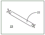
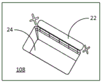
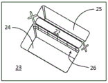
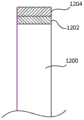
It is known to provide a deposited protective layer over the desired sheet location prior to thinning to protect the region of interest on the sample from exposure to the ion beam and to prevent bending or buckling. In one common fabrication technique, as shown in fig. 1-3, a protective layer 22 of a material, such as tungsten, carbon, or platinum, is first deposited over a region of interest on an upper surface 23 of a sample body using electron beam or ion beam deposition, as shown in fig. 1. Next, as shown in fig. 2 and 3, a focused ion beam of high beam current with a considerable beam size is used for milling away a large amount of material from the front and back of the region of interest. The remaining material between the two milled areas 24 and 25 forms a thin vertical sample area 26 comprising the region of interest. Typically, the region of interest is comprised 200-300 nm above the sample surface. The area 25 milled on the back of the region of interest is shown to be smaller than the front area 24. The smaller milled area 25 is primarily to save time, but also to prevent the finished sample from falling into the larger milled area 24, making it difficult to remove the sample area 26 from the sample body. The sample area 26 may then be cut out of the sample volume using a focused ion beam and then lifted out using, for example, a micromanipulator in a well known manner. The sample region 26 is then typically transferred to a TEM grid and thinned. The sample region 26 may then be analyzed using a TEM or other analysis tool.
There are significant problems in preparing ultra-thin (< 30 nm thickness) TEM samples. For example, the platinum protective layer over the region of interest is too soft and typically damaged during lamella thinning, being completely consumed by peripheral erosion from the ion beam tail before lamella thinning is completed. A harder material layer may be more resistant to erosion than a softer material, but may result in undesirable artifacts in the cross-section of the sheet.
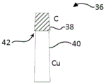
Fig. 4 and 5 show an example of a problem in the preparation of ultra-thin samples. As shown in fig. 4, a cross section of the sheet sample 30 is shown fabricated with a soft Pt cap 32 deposited on a hard diamond substrate 34. This thickness mismatch causes the softer Pt cap 32 to erode faster than the harder diamond substrate 34 when the lamella 30 is made to the desired thickness dimension by thinning. This combination desirably prevents the user from thinning the sheet as much as possible, since the protective cover 32 is ultimately completely consumed before the substrate 34 is sufficiently thinned. In contrast, as shown in fig. 5, a cross section of the sheet sample 36 is shown fabricated with a hard carbon cap 38 placed on a soft copper substrate 40. In this example, a downcut 42 may be observed as the softer substrate 40 wears out faster than the harder cap 38. This can lead to premature failure of the sheet and artifacts such as "drooping" of the cross-sectional treated surface.
Sag is a posterior biology that causes rippling or unevenness in the sample surface. Droops may form for various reasons. If the sample is non-uniform, being composed of different materials with different sputtering rates, the harder material may form resistive areas that protrude slightly from the cross-section. These protrusions mask the area under them, resulting in downwardly developing vertical streaks. Fig. 6 shows sample 44 with a silicon substrate with a tungsten cap showing sag. "droop" results because tungsten is harder or more resistant to sputtering from the ion beam than the silicon substrate. This results in features that protrude slightly from the cross-section of the substrate. The harder overhanging tungsten substantially masks the substrate directly below it, resulting in a vertical protrusion of tungsten. Alternatively, some hard capping materials form a wave-mark-like or line-like pattern when exposed to an ion beam, even if the capping material itself is uniform inside. Fig. 7 shows sample 46 with a silicon substrate with a carbon protective layer showing sag. When cross-sectional milling is performed, the carbon layer material gradually exhibits a highly textured surface. Thus, the morphology of the carbon layer leads to the sag in this example. Thinning of the sample from top to bottom with these types of structures or density variations results in the acquisition of vertical ridges or variations that develop down the cross-section from denser material (i.e., metal lines) near the top of the sample (the top being defined as closest to the ion beam source), which runs parallel to the direction of the ion beam. Sag is most often observed in semiconductor materials where multiple patterned layers of materials with low sputtering yield hinder faster sputtering yield (sputtering yield) materials. Sag may also be observed in materials showing different morphological regions, where the variation in sputtering yield varies with milling incidence angle. Samples with holes also induced sag. Post-sag organisms degrade TEM imaging and limit the minimum usable sample thickness.
Another type of post-bio is known as a "golf tee". For example a layer of tungsten or carbon, typically a material such as silicon, on a region of interest on a sample. The cap material and silicon substrate have different "hardnesses" (resistance to sputtering from the ion beam) resulting in a top to bottom thickness variation, known as "golf-pegs" (where the sample is thicker at the top and narrows to a thinner dimension so that the sample has a "golf-peg" profile when viewed in a Y-section. Since the region of interest is typically contained near the upper surface of the slice, a thicker dimension can mask the region of interest and result in less than desired sample for TEM observation.
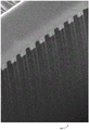
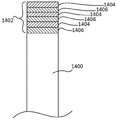
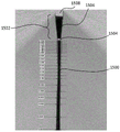
A sample of the "golf tee" effect can be seen in fig. 8, which shows a TEM sample 50 having an Ion Beam Induced Deposition (IBID) tungsten protective layer 52 located on the upper surface of the sample 50. In this sample, sample 50 was 44 nm wide directly under protective layer 52 and narrowed to 25 nm wide at 150 nm under protective layer 52 after thinning. This thickness variation is a result of the different etch rates between the silicon substrate and the tungsten cap layer. Tungsten is a harder, denser material than silicon and has a significantly lower etch rate, which results in the tungsten protective layer 52 being wider than the bulk of the wafer. Typically, the region of interest is located in the main region, where the "golf tee" obscures or interferes with the region of interest for TEM observation.
What is needed is an improved method of material deposition to achieve a controlled workpiece surface free of surface artifacts and slope variations.
Summary of The Invention
It is an object of the present invention to provide an improved method and apparatus for forming a protective layer for charged particle beam treatment to expose a region of interest for viewing.
A system for processing a workpiece with a charged particle beam to expose a region of interest for observation, including a method and apparatus for providing a precursor gas at a surface of the workpiece; directing a beam of charged particles toward a substrate to induce deposition of a protective layer from a precursor gas over a region of interest, the protective layer being composed of at least two different materials having different sputtering rates; a charged particle beam is directed at the substrate to mill the protective layer to expose a region of interest beneath the protective layer.
The foregoing has outlined rather broadly the features and technical advantages of the present invention in order that the detailed description of the invention that follows may be better understood. Additional features and advantages of the invention will be described hereinafter. It should be appreciated by those skilled in the art that the conception and specific embodiment disclosed may be readily utilized as a basis for modifying or designing other structures for carrying out the same purposes of the present invention. It should be realized by those skilled in the art that such equivalent constructions do not depart from the scope of the invention as set forth in the appended claims.
Brief Description of Drawings
This patent or application file contains at least one drawing executed in color. Copies of this patent or patent application publication with color drawing(s) will be provided by the office upon request and payment of the necessary fee. For a more complete understanding of the present invention and the advantages thereof, reference is now made to the following descriptions taken in conjunction with the accompanying drawings, in which:
fig. 1-3 illustrate steps in ex situ sample preparation techniques according to the prior art.
Figure 4 shows a prior art sheet profile with a hard diamond substrate and a readily consumable soft platinum top layer.
Figure 5 shows a prior art sheet profile with a soft copper substrate and a hard carbon top layer with a resulting fell cut.
Fig. 6 is a photomicrograph showing a dropped FIB section with a tungsten top layer, according to the prior art.
Fig. 7 is a micrograph showing a thinned TEM sample with a carbon top layer hanging down according to the prior art.
Fig. 8 shows an image of a sheet with a "golf tee" back creature after thinning according to the prior art.
Fig. 9 illustrates a charged particle beam system with a Multiple Gas Injection System (MGIS).
Fig. 10 shows contour plots of vertical deposition growth rate as a function of valve duty cycle for Pt precursor (X-axis) and C precursor (Y-axis).
FIG. 11 shows a contour plot of the sputter rate of the deposited C-Pt composite as a function of the valve duty cycle of the Pt precursor (X-axis) and the C precursor (Y-axis).
Figure 12 shows the ply profile with a C-rich protective composite layer.
Fig. 13 shows the sheet profile with a Pt-rich protective composite layer.
Fig. 14 shows the sheet profile of the protective composite layer with C-Pt.
Fig. 15 illustrates an embodiment of composite material deposition for a substrate having a shaped via structure.
Fig. 16 illustrates another embodiment of composite deposition for a substrate having a shaped via structure.
Fig. 17 illustrates another embodiment of composite deposition for a substrate having a shaped via structure.
Fig. 18 shows the valve duty cycle for the composite deposition of fig. 17.
Fig. 19 illustrates another embodiment of composite material deposition for a substrate having a shaped via structure.
FIG. 20 shows a valve duty cycle for the composite material deposition of FIG. 19.
Figure 21 shows another embodiment using a dual beam system of the type used to carry out the present invention.
Fig. 22 shows the sheet profile of protective layers with different materials.
Fig. 23 shows the sheet profile with multiple protective layers of different materials.
Fig. 24 shows the sheet profile of the protective layer with different alternating materials.
FIG. 25 shows an image of a preferred embodiment of a sheet having multiple protective layers.
FIG. 26 shows a photomicrograph of another preferred embodiment of a sheet having multiple protective layers.
Fig. 27A and 27B show plots of the data in tables 1 and 2.
Fig. 28 shows a flow chart of material deposition according to the present invention.
Description of The Preferred Embodiment
Embodiments of the present invention provide an improved protective layer for charged particle beam processing by using two different materials to create the protective layer.
According to one embodiment, the material deposition is performed to provide a layer of protective material having a sputtering rate that substantially matches the sputtering rate of the substrate material. A charged particle beam is directed at the substrate in a vacuum chamber of the FIB system to induce material deposition from the precursor gas mixture. The resistance to sputtering of the protective layer material deposition can be adjusted by varying the ratio of the gas mixture components. A multi-gas injection system with variable flow control and mixing capability is used that is capable of varying the precursor ratio over a wide range depending on the material of the sample substrate to vary the hardness of the protective layer material.
According to another embodiment, material deposition is performed to provide a protective layer comprising two or more material compositions deposited in multiple layers, wherein each layer has a different etch rate. Preferably, the charged particle beam is directed towards the substrate in a vacuum chamber of the FIB system to induce deposition of the first protective layer onto the sample substrate from the precursor gas over the region of interest. An ion beam is then directed at the sample substrate to induce deposition of at least a second protective layer on the first protective layer from the precursor gas. Preferably, the first protective layer has an etch rate closely matching the etch rate of the sample, and the second protective layer (and any other layers) has an etch rate different from the etch rate of the sample. For example, for a softer substrate, the softer protective material may first be deposited in direct contact with the substrate, and then a second harder layer may be deposited on the first layer. The harder layer resists erosion from the ion beam while the softer bottom layer resists cross-sectional artifacts. An underlayer having a sputtering rate that closely matches the sputtering rate of the substrate reduces the risk of cross-sectional artifacts after processing. For harder substrates, such as diamond, carbon, or silicon carbide, a harder protective layer may be deposited first to be in direct contact with the substrate, with a softer layer of material deposited on the first layer.
In another embodiment, material deposition is performed to provide alternating layers of material to form the protective layer, wherein the etch rate of the protective layer material is "tuned" by depositing alternating thin layers of material using separate (discrete) gas chemistries, which form alternating "parfait-like" macrostructures with etch rates between the etch rates of the individual components. By adjusting the thickness of the individual components and the total number of layers, the user can achieve a degree of adjustability to achieve the desired film properties. Ultra-thin alternating layers of infinite (limiting extreme) can be deposited, resulting in the deposition of a composite-like mixture.
In another embodiment, a mixture of gas precursors is used in the material deposition, but the ratio of gases is gradually adjusted during the deposition process to form a composite capping material such that the bottom of the protective layer is predominantly one component and the top of the layer is predominantly another component, with the middle region having an intermediate composition. As milling progresses over the protective material, a gradual transition from hard to soft (or vice versa) is provided.
In another embodiment, the material deposition methods described herein can be performed using TEM lamella preparation to adjust the stiffness of the sacrificial protective cap to prevent damage to the lamella due to erosion from the beam tail, and can minimize cross-sectional processing artifacts such as sag and sidewall slope variation at the interface.
In another embodiment, the material deposition methods described herein may be performed with applications in which the composite capping layer is generally used to form a single-sided FIB section, having a cut surface free of defects and grade variations.
In another embodiment, the material deposition methods described herein can be performed with applications in which a composition-deposited film can be used to control the milled profile of high aspect ratio structures (e.g., vias) formed using ion beam milling.
According to a first preferred embodiment of the present invention, a substrate, such as a semiconductor chip, is loaded into a dual beam FIB/SEM system having a FIB column and an SEM column. Although a dual beam system is discussed, it is understood that the invention may be practiced using other FIB systems. The chips may be transferred manually or preferably by means of a multi-chip carrier and an automatic loading robot (not shown).
In applications for preparing a slice sample, the location of the region on the sample containing the feature of interest for extraction and analysis (i.e., the slice location) is determined. For example, the substrate may be a semiconductor chip or a portion thereof, and the sample to be extracted may comprise a portion of an integrated circuit to be viewed using TEM. Typically, the substrate is roughly aligned by using machine vision to set the reference symbol position on the chip or wafer or using the edge of the unpatterned chip and an alignment notch or plane. Alternatively, the slice position may be set automatically using image recognition software. Suitable image recognition software is available from Cognex Corporation of Natick, MA. The image recognition software can be "modulated" to set the position of the desired slice, either by using a sample image of a similar part or by using geometric information from CAD data. Automated FIB or SEM metrology may also be used to identify or help identify the slice locations. Metrology can consist of image-based pattern recognition, edge detection, ADR, centroid calculation, or speckle. If desired, fiducial marks can be milled into the substrate surface as precise and accurate positioning marks.
A composite protective layer is then deposited over the sheet locations to protect the sample. In a first preferred embodiment, the IBID or EBID deposition can be performed using a multi-gas injection system, wherein two or more precursor gases are flowed simultaneously. For example, precipitation may be performed wherein the deposited material has properties intermediate between two individual components. For example, an IBID deposition obtained with a mixture of Pt and C precursors may be carried out to obtain a protective layer having properties intermediate to those obtained with Pt and C precursors alone. Precursor mixing can be performed in a variety of ways. For example, a single gas nozzle outlet may be shared by two or more vessels containing respective chemical precursors, and the relative flow rates of the respective components may be controlled by a pulse valve located between the chemical precursor vessels and the outlet.
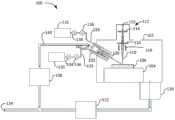
Fig. 9 shows a schematic representation of a beam system 100 incorporating an embodiment of the present invention. The beam system 100 includes a sample vacuum chamber 102, which contains a sample stage 104 for supporting a workpiece 106 to be processed by a beam 110,the beam 110 is produced by a beam generating subsystem such as a laser or charged particle beam column. For example, charged particle beam column 112 includes a charged particle source 113, one or more focusing lenses 114, and a deflector 116 for scanning or otherwise directing beam 110 in a specified pattern over the surface of a workpiece. The evacuation system, e.g., combination of high vacuum vane pump 120 and backing pump 122, is maintained preferably below 10 deg.f during processing in the sample vacuum chamber 102-3mbar, more preferably less than 10-4mbar, even more preferably less than or equal to about 10-5Vacuum of mbar. The backing pump 122 exhausts to an exhaust 124.
Gas is supplied to a localized area of the workpiece surface through a retractable needle 130 (which is described in more detail below) extending from a Multiple Gas Injection System (MGIS) valve 132. Gases, such as deposition precursor gases, etching precursor gases or inert purge gases, are stored in the gas reservoirs 131. The term "reservoir" is used broadly to include any source of gas. Some of the reservoirs 131 may include a solid or liquid material heated, for example, in a crucible to derive a desired gas, while other reservoirs 131 may include a compressed gas. Each reservoir 131 is connected to the MGIS valve 132 by a respective conduit 133, with a regulating valve 134 and a shut-off valve 136 in the flow path between each reservoir 131 and the MGIS valve 132. Although fig. 9 shows two reservoirs with corresponding conduits, the invention is not limited to any number of reservoirs. Some embodiments of the invention use six or more reservoirs, while other embodiments may use a single gas source.
When the preset gas recipe is executed, the MGIS valve 132 needle 130 is extended and process gas flows through the needle 130 from the valve 132 to the surface of the workpiece 106 near the point where the charged particle beam 110 is focused.
The sample stage 104 is used to place a workpiece under the charged particle beam 110 and the needle 130. Finally, gas from the needle 130 in the sample vacuum chamber is pumped from the chamber by the vane pump 120. A vacuum pump 138 removes residual gases from the interior of the MGIS valve through an MGIS vacuum conduit 140 equipped with an MGIS vacuum valve 142.
A particular solution for a composite protective layer consists of a specific ratio (depending on the material of the sample substrate) of mixed precursors. Preferably, one precursor will yield a relatively soft deposition material and the other precursor will yield a relatively hard deposition material. Thus, the user can adjust the deposited layer thickness to any value between the properties of each individual precursor. The precursors are mixed at a ratio to match the sputtering rate of the protective layer material to that of the substrate material to achieve sufficient thinning and prevent interfacial artifacts. The duty cycle of the valve in the MGIS delivery hardware can be continuously varied between 0% and 100%. Thus, the deposition material may be tailored to have properties intermediate to those of the individual mixed precursor components. This results in a customized deposition for different substrate materials and different applications.
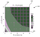
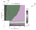
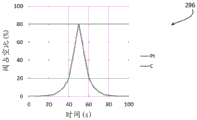
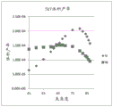
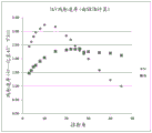
In one example, a protective carbon-platinum (C-Pt) layer is deposited. The C-Pt precursor is mixed in a specific ratio depending on the material of the substrate. This is achieved by adjusting the C-Pt ratio as shown in the contour plots shown in FIGS. 10 and 11. In fig. 10, a contour plot 150 of vertical deposition growth rate (nm/sec) as a function of valve duty cycle for Pt precursor (X-axis) and C precursor (Y-axis) is shown. Circle 152 represents the highest growth rate, and circles 154 and 156, which relate to Pt and C, respectively, represent the growth rate of a standard single precursor material. In FIG. 11, a contour plot 160 showing the sputter rate of the deposited C-Pt composite as a function of the valve duty cycles of the Pt precursor (X-axis) and the C precursor (Y-axis) is shown. Circles 162 and 164, which relate to Pt and C, respectively, represent the sputtering rate of a standard single precursor material. Adding a small amount of Pt to the majority of the C deposition, as marked by circle 166, for example, results in a superior material to either individual component as a protective cap layer. This layer is much harder than Pt alone, but does not have the drooping effect of C alone. Variable duty cycle valve control or percentage of "on" time of the pulsing valve, and the mixing capability of the multi-gas injection system enable such adjustments. Therefore, a desired "hardness" can be achieved by moving from the upper left to the lower right of the contour diagram 160 in fig. 11. Thus, the user can tailor the hardness of the deposited layer to suit the sample, in particular to match the hardness of the sample substrate.
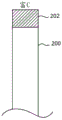
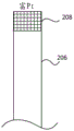
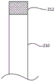
For example, as shown in fig. 12-14, C-Pt composite deposits having various hardness properties were applied on a substrate. For example, a C-Pt composite can be formed on the substrate 200 by continuously adjusting the valve duty cycle to achieve a C-rich composite (C-valve duty = 80%, Pt-valve duty < 2%), resulting in a very hard protective layer 202 as shown in fig. 12 (but without separate C-hard). As shown in fig. 13, a C-Pt composite can be formed on the substrate 206 by continuously adjusting the valve duty cycle to achieve a Pt-rich composite (C valve duty cycle < 2%, Pt valve duty cycle = 80%), resulting in a very soft protective layer 208 (but not Pt alone soft). If a hard substrate sample is used, such as diamond, a C-rich layer can be deposited with a hardness closely matching the hardness of the diamond substrate. As an example shown in fig. 14, a substrate 210 with a capping layer of C-Pt material 212 deposited with an MGIS setting (C to Pt) of 80% -5% is preferred for layers obtained with pure C or pure Pt precursors. The 80% -5% ratio has a higher material growth rate than either C or Pt alone. In addition, this ratio has a higher sputtering resistance than Pt and has less sag than C.
Other deposits can be obtained for substrates having various hardness properties. For example, a protective layer with an intermediate duty cycle (e.g., 40% for both carbon and platinum) has properties that are roughly intermediate between those obtained with either individual component. For samples with softer substrate properties, such as organic resins, the deposition precursor can be adjusted to be Pt-rich.
Possible duty cycle and sample combinations include a medium hard silicon substrate with a deposited layer using a valve duty cycle of 50% -50% (C to Pt), a hard diamond substrate with a deposited layer using a valve duty cycle of 80% -1% (C to Pt), and a soft resin substrate with a deposited layer using a valve duty cycle of 5% -80% (C to Pt). The precursors can also be mixed with a conventional MGIS system, where the ratio of the precursors can be roughly adjusted by controlling the crucible temperature for each reagent. However, many duty cycle combinations are possible, these examples illustrate that the hardness of the deposited material can be continuously varied to match the hardness of the substrate material.
In addition to the pulsed valve mixing strategy described above, other precursor delivery methods may be used. For example, the relative flow rates of the individual precursor components may be adjusted using mass flow control valves, metering needle valves, or simply by adjusting the temperature of the precursor container to adjust the vapor pressure of the components. The flow rate can also be influenced by using orifices of different sizes (bore diameters) or by using pipes with different inner diameters. Finally, multiple precursor chemicals can be mixed in the same vessel, thereby opening the single valve to allow the mixture of precursor gases to be loaded into the vacuum chamber of the instrument. Regardless of the delivery strategy used to deliver the multi-component precursor mixture, the precursor mixture can be used to adjust the properties of the deposited material layer, regardless of the hardware or system used to form the mixture.
The layer of deposited material from the precursor mixture may be applied to a variety of different applications. In TEM lamella preparation, adjusting the stiffness of the sacrificial protective cap can prevent lamella damage due to erosion from the beam tail and can minimize cross-sectional post-processing artifacts such as drooping and golf tacks and sidewall slope variation at the interface. Another application for composite deposition is generally for forming single-sided FIB sections, with sections free of defects and slope variations.
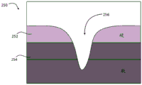
The composite deposition layer may also be used to control the milling profile of high aspect ratio structures (e.g., vias) formed using ion beam milling. This can be used for FIB nano-and micro-scale processing, or for ion beam printing techniques. In this application as shown in fig. 15, a workpiece 250 includes a thin composite deposited capping material 252 deposited onto a substrate 254, with a user desiring to form high aspect ratio structures, such as vias 256, in the substrate 254. A particular scheme should be chosen for composite deposition that is "harder" than the underlying target material. As milling initially begins, the ion beam penetrates deeper and deeper into the hard deposition layer 252. Finally, milling will reach the interface between the hard deposit 252 and the underlying soft substrate 254. At this point, milling of the underlying substrate 254 begins, but only in the center of the ion beam profile, where the milling speed is highest. Because the underlying substrate 254 is softer than the encapsulation material 252, and because the ion beam profile is substantially Gaussian, the soft material 254 should be rapidly milled through the center of the beam where the intensity of the ion beam is distributed, while the less intense "tail" of the ion beam still has not penetrated the harder encapsulation material 252.
Thus, the arrangement of the harder capping film on the softer target material has a sharpening effect on the shape of the ion milling probe, and a via having a narrower dimension can be obtained, which can be achieved with uncapped substrates. If desired, the top capping film may be removed in a final step, leaving a "sharpened" high aspect ratio mill. This can be achieved, for example, by using a hard carbon film over the silicon substrate, which can be removed using an oxygen plasma cleaning step. Thus, high aspect ratio structures with relatively narrow dimensions and parallel sidewalls may be formed.
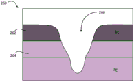
In another example, vias with chamfered or tapered profiles (top flash) may be formed by depositing a capping film that is softer than the underlying substrate. In the example shown in fig. 16, a workpiece 260 is shown having a capping layer 262 that is softer than an underlying substrate 264 formed with vias 266. The effect of the beam tail on the soft capping layer 262 creates a more outboard erosion resulting in a significant widening at the top of the via structure than a cap-less milled via.
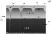
Fig. 17 shows an embodiment of a workpiece sample 280 having a silicon substrate 281 with a composite layer 282, forming a FIB-milled via 283 in the composite layer 282, where the composite layer 282 has a "hardness" that varies from bottom to top of the layer. Such composite layers may be formed by adjusting the duty cycle of each precursor component during deposition. For example, a Pt-C composite layer that varies from soft to hard (bottom to top) can be deposited by starting with a deposition of a Pt-rich mixture and gradually transitioning to a C-rich mixture as the deposition growth progresses. The valve duty cycle for such a process is shown by graph 286 in fig. 18.
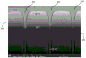
Fig. 19 shows the reverse process of forming a FIB-milled via 293 in a composite layer 292 using a workpiece sample 290 having a silicon substrate 291 with the composite layer 292, where the composite layer 292 has a "hardness" that varies from the bottom to the top of the layer. Such composite layers may be formed by adjusting the duty cycle of each precursor component during deposition. For example, a Pt-C composite layer that varies from hard to soft (bottom to top) can be deposited by starting with a deposition of a C-rich mixture and gradually transitioning to a Pt-rich mixture as the deposition growth progresses. The valve duty cycle for such a process is shown in fig. 20 by graph 296.
Although Pt-C mixtures have been discussed as examples of composite layers, it should be understood that other precursor combinations result in deposited layers that also have variable material properties. For example, a carbon-platinum complex can be obtained using precursors of naphthalene and (methylcyclopentadienyl) trimethylplatinum. Naphthalene and W (CO) may be used6The precursor yields a carbon-tungsten composite. (methylcyclopentadienyl) trimethylplatinum and W (CO)6The precursors lead to platinum-tungsten composites, carbon-SiOx composites can be obtained using naphthalene and TEOS or TMCTS or HMCHS precursors.
The "hardness" of the dielectric deposition can be adjusted, which is typically performed using a siloxane-based precursor and an oxidizing agent. High concentrations of oxidizing agent will result in a fully saturated SiO2The layer deposited stoichiometrically, whereas the layer deposited with a reduced amount of oxidizer is not fully saturated and has a stoichiometric SiOxIn which X is<2. Any of the following siloxane-oxidant combinations are suitable for such conditioning: TEOS (tetraethyl orthosilicate) and O2(ii) a TMCTS (tetramethylcyclotetrasiloxane) and N2O; and HMCHS (hexamethylcyclohexasiloxane) and water. However, any siloxane can be used with any oxidizing agent.
A plasma FIB instrument that generates any of the following primary ions: o is+、O2 +、O3 +、N+、N2 +、H2O+、H2O2 +、N2O+、NO+、NO2 +(ii) a Can potentially be used in conjunction with siloxane precursors to deposit dielectric layers of varying hardness. In this case, the oxidizing agent itself is of the primary beam type. Thus, the deposited layer can be made to range from fully saturated SiO by adjusting the beam density, precursor flux, and/or ion beam energy during deposition2Stoichiometric to less saturated SiOx(X<2) And (4) stoichiometry.
It should be understood that although the above examples discuss modulating the material "hardness," or resistance to sputtering from an ion beam, other material properties may be adjusted using the same method. For example, the resistivity of the dielectric film increases with increasing oxidant concentration. Thus, by controlling the siloxane-oxidant mixture, a user can deposit a film with nearly electrical conductivity. The optical transparency of the deposited film is another property that can be modulated by precursor mixing. In addition, material deposition using the disclosed methods can be obtained by laser-assisted precursor decomposition or by thermal decomposition on a heated surface.
According to a second preferred embodiment of the present invention, a substrate, such as a semiconductor chip, is loaded into a dual beam FIB/SEM system having a FIB column and an SEM column. A typical dual beam system configuration includes an electron column having a longitudinal axis and an ion column having an axis that is tilted with respect to vertical (typically at a tilt of about 52 degrees). One such system is the DualBeamTMThe Helios family of Systems, commercially available from FEI corporation of Hillsboro, OR, the assignee of the present invention.
FIG. 21 illustrates an exemplary dual-beam FIB/SEM system 2110 suitable for implementing the present invention. The system 2110 includes an evacuated envelope having an upper neck portion 2112, with a liquid metal ion source 2114 or other ion source and a focusing column 2116 disposed within the upper neck portion 2112. Other types of ion sources may be used, such as multiple cusp (multicusp) or other plasma sources, and other optical columns, such as shaped beam columns, as well as electron beam and laser systems.
The ion beam 2118 is moved from the liquid metal ion source 2114 through an ion beam focusing column 2116 and between electrostatic deflection tools illustrated at a deflection plate 2120 toward a substrate or workpiece 2122, which substrate or workpiece 2122 includes, for example, a semiconductor device located on a stage 2124 within a lower chamber 2126. Stage 2124 may also support one or more TEM sample supports so that a sample may be extracted from the semiconductor device and moved to the TEM sample supports. The stage 2124 is movable, preferably in a horizontal plane (X and Y axes) and a vertical direction (Z axis). In some systems, the stage 2124 may also be tilted at approximately sixty (60) degrees and rotated about the Z-axis. The system controller 2119 controls the operation of the various parts of the FIB system 2110. Through a system controller 2119, a user can control the ion beam 2118 which is scanned in a desired manner through commands entering a conventional user interface (not shown). Alternatively, the system controller 2119 may control the FIB system 2110 in accordance with programmed instructions stored in a computer readable memory, such as RAM, ROM, or magnetic or optical disk. The memory may store instructions for performing the above-described methods in an automated or semi-automated manner. The image from the SEM can be recognized by software to decide when to continue processing, when to stop processing, and where to place the beam for milling.
For example, the user may define a region of interest on a display screen using a pointing device, and the system may then automatically perform the steps described below to extract the sample. In some embodiments, the FIB system 2110 incorporates image recognition software, such as that commercially available from Cognex Corporation, Natick, Massachusetts, to automatically identify regions of interest, which can then be used to manually or automatically extract samples in accordance with the present invention. For example, the system may automatically place similar components on a semiconductor chip (including multiple devices) and sample those components on different (or the same) devices.
An ion pump 2128 is used to evacuate the upper neck portion 2112. The lower chamber 2126 is evacuated using a turbomolecular and mechanical pumping system 2130 under the control of a vacuum controller 2132. The vacuum system provides about 1 x 10 in the lower chamber 2126-7 Torr (1.3 x 10⁻⁷mbar) to 5 x 10⁻⁴ Torr (6.7 x 10⁻⁴mbar). The chamber background pressure can be raised, typically to about 1 x 10, for the deposition precursor gas or if an etch-assist gas or etch-stop gas is used-5 Torr (1.3 x 10⁻⁵ mbar)。
A high voltage power supply 2134 is connected to the liquid metal ion source 2114 and occupies electrodes in the ion beam focusing column 2116 for forming and directing an ion beam 2118 of about 1 keV to 60 keV to the sample. A deflection controller and amplifier 2136, operating according to a prescribed pattern provided by a pattern generator 2138, is coupled to the deflection plate 2120, wherein an ion beam 2118 provided by the pattern generator 2138 is coupled to the deflection plate 2120, wherein the ion beam 2118 can be manually or automatically controlled to find a corresponding pattern on the upper surface of the workpiece 2122. In some systems, a deflection plate is placed in front of the final lens as is well known in the art. Beam blanking electrodes (not shown) within the ion beam focusing column 2116 cause the ion beam 2118 to strike a blanking aperture (not shown) instead of the target 2122 when a blanking controller (not shown) applies a blanking voltage to the blanking electrodes.
The liquid metal ion source 2114 typically provides a metal ion beam of gallium. The source is typically capable of focusing into a tenth-micron wide beamlet on the workpiece 2122 for modifying the workpiece 2122 by ion milling, modified etching, material deposition, or for the purpose of imaging the workpiece 2122. If desired, the charged particle detector 2140 may be used to detect secondary ion or electron emissions to be connected to the video circuit 2142 (providing a drive signal to the video monitor 2144) and receive deflection signals from the controller 2119.
The placement of the charged particle detector 2140 within the lower chamber 2126 can vary in different embodiments. For example, the charged particle detector 2140 may be coaxial with the ion beam and include a hole for the ion beam to pass through. In other embodiments, the secondary particles may be collected by a final lens and then off axis for collection. A Scanning Electron Microscope (SEM) 2141 is optionally provided with its power supply and controls 2145 along with the FIB system 2110.
A gas delivery system 2146 extends into the lower chamber 2126 for introducing and directing the vapor toward the workpiece 2122. U.S. Pat. No. 5,851,413 to Casella et al ("Gas Delivery Systems for Particle Beam Processing"), assigned to the assignee of the present invention, describes a suitable Gas Delivery system 2146. Another Gas delivery System is described in U.S. Pat. No. 5,435,850 ("Gas Injection System"), to Rasmussen, also assigned to the assignee of the present invention. For example, iodine may be delivered to improve etching, or a metal organic compound may be delivered to deposit a metal.
The door 2160 is opened for insertion of the workpiece 2122 onto the X-Y table 2124, which may be heated or cooled, and also for servicing the internal supply air reservoir (if used). The door can be interlocked so that it cannot open if the system is under vacuum. In some embodiments, an atmospheric chip operating system may be used. The high voltage power supply provides appropriate acceleration voltages to electrodes in the ion beam focusing column 2116 for exciting and focusing the ion beam 2118. When it strikes the workpiece 2122, material is sputtered from the sample, which is a physical jet. Alternatively, the ion beam 2118 can decompose a precursor gas to deposit a material. Focused ion beam systems are commercially available, for example from FEI Company, Hillsboro, Oregon (assignee of the present application). Although examples of suitable hardware are provided above, the invention is not limited to implementation in any specific type of hardware.
In this embodiment, the material deposition may be performed by forming two or more different layers of protective cap material. The user may first choose to deposit the "softer" material in direct contact with the underlying substrate, and then may deposit a second "harder" layer on top of the first layer. The harder top layer resists erosion from the ion beam while the softer bottom layer prevents cross-sectional artifacts. In particular, if the underlayer can be chosen to match the sputtering rate of the underlying material, the risk of cross-sectional post-processing organisms can be minimized. In other cases, the order may be reversed, with harder material deposited first, followed by softer material. This arrangement may be preferred when FIB milling hard materials such as diamond, carbon or silicon carbide.
For example, as shown in FIG. 22, the sheet substrate 1200 has a protective layer of material (withWith a bottom layer 1202), the bottom layer 1202 is first deposited onto the upper surface of the substrate 1200, preferably using Electron Beam Induced Deposition (EBID), to prevent damage to upper regions of the substrate 1200 near the upper surface where the region of interest is primarily located. An alternative is to use low energy (<8 keV) IBID, which also results in very low damage to the upper surface. In some processes, low energy FIB deposition is used instead of EBID. The first underlying material 1202 is selected to match as closely as possible the etch rate of the material of the substrate 1200, particularly in<5kV FIB @ 10-45 degrees off grazing angle. For silicon (Si) -based samples, the underlayer 1202 is preferably a silicon oxide material of the type such as TEOS (IDEP), TEOS + H2O (IDEP2)、TEOS+O2、HMCHS、HMCHS+O2 (IDEP3)、HMCHS/H2O and HMCHS/N2O、TMCTS、TMCTS+O2And/or TMCTS/H2O、TMCTS/N2And O. The top layer material 1204 is then deposited on the bottom layer 1202 using Ion Beam Induced Deposition (IBID). Top layer material 1204 is selected to have a lower etch rate than the material of substrate 1200 to provide protection during lamella thinning and to prevent post-formation on the outer surface of the sample.
More than one top layer may be deposited if desired. The one or more top layers are preferably tungsten, carbon or platinum. As an example, carbon has excellent resistance to low kV FIB milling for good protection, but with significant internal stress that may wrap the sheet. Therefore, a pure carbon layer is not desirable. However, as shown in fig. 23, the substrate 1300 has a protective layer that includes an underlayer 1302 of material similar to the layer 1202 discussed with reference to fig. 22. A thin carbon layer 1304 (e.g., a 100 nm C layer after 30 kV processing) on a thicker tungsten layer 1306 (e.g., about 400 nm) presents better low kV FIB emission than tungsten alone, and tungsten provides hardness to the lamellae. In the 35 degree sweep range, which is the angle of the FIB beam to the lamella sidewalls, the silicon substrate etch rate is significantly higher than tungsten, which typically results in a golf pinning effect that makes the lamella top much thicker than the area a few hundred nanometers below the sample surface. The qualitative curves of the angle-dependent sputtering rates for silicon and tungsten can be seen in the table below.
Tables 1 and 2 below show sputtering and volume yield from 5kV gallium ions. The data in tables 1 and 2 are plotted in fig. 27A and 27B.

TABLE 1

Table 2.
In another embodiment of the multi-layer deposition strategy, multiple layers may be deposited in an alternating configuration. Stacking multiple layers of different deposition materials can result in obtaining a layer that on average has properties intermediate between two separate components. By adjusting the thickness of the individual components and the total number of layers, a user can achieve a degree of adjustability to achieve desired layer properties. Generally, the desired film properties are intermediate values for the individual components. For example, if platinum is too soft and carbon is too hard for a particular application, multi-layer deposition of alternating platinum and carbon depositions may be preferred for a uniform layer of either of the individual components.
Fig. 24 illustrates such an embodiment where the substrate 1400 comprises a material deposition of a protective layer 1402 with alternating layers 1404, 1406 of material, wherein the etch rate of the protective layer material 1402 is "tuned" by depositing the alternating thin layers 1404, 1406 of material using separate gas chemistries, thus forming a "parfait-like" macrostructure with an etch rate that alternates between the etch rates of the individual components.
Fig. 25 shows an image of a substrate 1500 having a sacrificial protective layer 1502 with separate layers, the sacrificial protective layer 1502 including a tungsten layer 1504, a SEM-deposited sacrificial layer of silicon oxide 1506, and a top layer of tungsten 1508 for visualizing the profile between the top of the substrate 1500 and the protective layer 1502. As can be seen, after thinning, the "golf tee" effect occurs within sacrificial protective layer 1502 and not within substrate 1500.
FIG. 26 shows a silicon wafer layer with an EBID TEOS layer, an IBID tungsten layer, and an IBID carbon layer.
In the embodiment of fig. 12-16, a sacrificial protective layer having a similar etch rate as the substrate sample moves the golf tee up into the protective layer and away from the top of the substrate including the region of interest for viewing and analysis.
As shown in fig. 28, the present invention provides a material deposition method in which a sample is loaded 1600 into a selected beam system. At least two precursor gases are provided for material deposition 1602. In decision block 1604, it is determined whether the deposited material is in a different layer or as a composite layer. If a different layer 1606 is deposited, a first layer is deposited over sample 1608, and then another layer 1610 is deposited. If only two layers are to be deposited, decision 1612 to end is determined at 1616, and the process is complete 1618. If more than two layers are deposited, a decision is made not to end 1614 and the process passes to block 1608 and continues until a decision is made to end 1616 and the process is completed 1618. If a composite layer 1620 is deposited, at least two precursor gases 1622 are mixed according to a determined scheme and a composite layer 1624 is deposited onto the sample and the process ends 1626.
Some embodiments provide a method of treating a workpiece with a charged particle beam to expose a region of interest for observation, comprising:
providing at least two precursor gases at the surface of the workpiece;
directing a beam of charged particles toward the substrate to induce deposition of a protective layer over the region of interest from at least two precursor gases, the protective layer being composed of at least two materials having different sputtering rates, the at least two materials being deposited by decomposition of at least two different precursor gases; and
a charged particle beam is directed at the substrate to mill the protective layer to expose a region of interest beneath the protective layer.
In some embodiments, providing at least two precursor gases at the surface of the workpiece includes providing at least two precursor gases simultaneously.
In some embodiments, providing at least two precursor gases at the surface of the workpiece includes sequentially providing at least two precursor gases.
In some embodiments, providing at least two precursor gases at a surface of a workpiece and directing a charged particle beam toward a substrate to induce deposition of a protective layer from the at least two precursor gases comprises:
providing a first precursor gas at a surface of a workpiece;
directing a beam of charged particles toward a substrate to induce deposition of a first material having a first sputtering rate from a first precursor gas;
providing a second precursor gas at the surface of the workpiece; and
directing a beam of charged particles toward the substrate to induce deposition of a second material having a second sputtering rate from a second precursor gas;
thereby creating a protective layer having a first material layer and a second material layer.
In some embodiments, the first material comprises silicon oxide.
In some embodiments, the second material comprises tungsten, carbon, or platinum.
In some embodiments, the protective layer comprises alternating layers of each material.
In some embodiments, the sputtering rate of the first material matches the sputtering rate of the workpiece, and the sputtering rate of the second material is lower than the sputtering rate of the first material.
In some embodiments, providing at least two precursor gases at the surface of the workpiece includes providing a mixture of a plurality of gas types.
In some embodiments, the mixture of multiple gas types includes a mixture of a platinum precursor and a carbon precursor.
In some embodiments, the mixture of gas types includes a mixture of a platinum precursor and a silicon oxide precursor.
In some embodiments, the relative amounts of the plurality of gas types in the mixture of the plurality of gas types is varied during deposition of the protective layer, thereby providing a protective layer with a composition that differs at different depths of the protective layer.
In some embodiments, the portion of the protective layer on the surface of the workpiece is softer than the top of the protective layer.
In some embodiments, directing a charged particle beam toward the substrate to mill the protective layer to expose a region of interest beneath the protective layer includes creating lamellae having a thickness of less than 200 nm.
In some embodiments, directing a charged particle beam toward the substrate to mill the protective layer to expose a region of interest beneath the protective layer includes generating a cross-section of a portion of the workpiece for observation on a scanning electron microscope.
Some embodiments provide a focused ion beam system for analyzing a workpiece, comprising:
an ion beam system comprising an ion beam source;
an ion beam column for focusing the ion beam onto the substrate;
a gas source for providing a precursor gas at a surface of the workpiece;
a processor for controlling the focused ion beam system according to stored instructions; and
a computer readable memory storing computer instructions for performing the above-described method.
Although the description above relates primarily to the deposition of a protective layer, the method is stable and repeatable and therefore amenable to automation, it will be appreciated that apparatus for performing the operations of the method are further within the scope of the invention. Although the material deposition method has been described as being performed using a dual beam system, it should be understood that the material deposition methods described herein may be performed by independently operated SEM systems or independently operated FIB systems of any ion polarity. It should further be understood that most beam depositions are not completely pure and may also contain "impurities" (e.g., precursor fragments), hydrocarbon incorporation, porosity, and density variations, which may result in deviations from the theoretical model of sputter hardness. Furthermore, it should be appreciated that embodiments of the present invention can be implemented by computer hardware or software, or a combination of both. The methods may be performed in a computer program according to the methods and figures described in this specification using standard programming techniques, including a computer readable storage medium constructed with the computer program, where the storage medium is constructed to cause a computer to perform in a specific and predefined manner. Each program may be implemented in a high level procedural or object oriented programming language to communicate with a computer system. However, the programs can be executed in assembly or machine language, if desired. In any case, the language may be a compiled or interpreted language. Further, the program may run on a designated integrated circuit that is programmed for this purpose.
The preferred methods or apparatus of the present invention have many new aspects and, since the invention can be practiced in different methods or apparatus for different purposes, not every aspect need be present in every embodiment. In addition, many aspects of the described embodiments may be separately patentable. The present invention has wide applicability and can provide many of the benefits described and illustrated in the embodiments above. The embodiments vary greatly depending upon the particular application, and not every embodiment provides all of the benefits and meets all of the objectives achievable by the present invention.
It should be appreciated that embodiments of the present invention can be implemented by computer hardware, a combination of hardware and software, or by computer instructions stored in a non-transitory computer-readable memory. The methods may be implemented in a computer program using standard programming techniques, including a non-transitory computer-readable storage medium constructed with the computer program, wherein the storage medium is configured to cause a computer to operate in a specific and predefined manner according to the methods and figures described herein. Each program may be implemented in a high level procedural or object oriented programming language to communicate with a computer system. However, the program(s) can be implemented in assembly or machine language, if desired. In any case, the language may be a compiled or interpreted language. Further, the program may run on a specific integrated circuit programmed for this purpose.
Further, embodiments may be implemented in any type of computing platform including, but not limited to, a personal computer, a minicomputer, a mainframe, a workstation, a networked or distributed computing environment, separate, integrated, or in communication with charged particle tools or other visualization devices, and the like. Aspects of the invention may be embodied in machine-readable code stored on a non-transitory storage medium or device (whether removable or integral to a computer platform, e.g., hard disk, optical read and/or write storage media, RAM, ROM, etc.), such that it is readable by a programmable computer, for constructing and operating a computer upon which the storage medium or device is read by the computer to perform the procedures described herein. Further, the machine-readable code, or portions thereof, may be transmitted over a wired or wireless network. The invention described herein includes these and other various types of non-transitory computer-readable storage media when such media contain instructions or programs for implementing the above-described steps, as well as a microprocessor or other data processor. The invention also includes the computer itself when programmed according to the methods and techniques described herein.
The terms "workpiece", "sample", "substrate" and "specimen" are used interchangeably herein, unless otherwise indicated. Further, whenever the terms "automatic," "automated," or similar terms are used herein, these terms are understood to include manual initiation of an automated or automated process or step.
In the following discussion and claims, the terms "include" and "comprise" are used in an open-ended fashion, and thus should be interpreted to mean "including, but not limited to. To the extent that any term is not specifically defined in this specification, it is intended to provide its plain and ordinary meaning. The accompanying drawings are intended to assist in understanding the invention and, unless otherwise indicated, are not drawn to scale. Particle beam systems suitable for carrying out the present invention are commercially available, for example, from FEI Company, the assignee of the present application.
Although the present invention and its advantages have been described in detail, it should be understood that various changes, substitutions and alterations can be made herein without departing from the scope of the invention as defined by the appended claims. Moreover, the scope of the present application is not intended to be limited to the particular embodiments of the process, machine, manufacture, composition of matter, means, methods and steps described in the specification. As one of ordinary skill in the art will readily appreciate from the disclosure of the present invention, processes, machines, manufacture, compositions of matter, means, methods, or steps, presently existing or later to be developed that perform substantially the same function or achieve substantially the same result as the corresponding embodiments described herein may be utilized according to the present invention. Accordingly, the appended claims are intended to include within their scope such processes, machines, manufacture, compositions of matter, means, methods, or steps.
Claims (16)
1. A method of processing a workpiece with a charged particle beam to expose a region of interest for viewing, comprising:
providing at least two precursor gases at a surface of a workpiece via a multi-gas injection system;
directing a beam of charged particles toward a substrate to induce deposition of a protective layer over the region of interest from at least two precursor gases, the protective layer being composed of at least two materials having different sputtering rates, the at least two materials being deposited by decomposition of at least two different precursor gases, wherein the protective layer comprises a composite mixture of the at least two materials or alternating layers of the at least two materials; and
a charged particle beam is directed at the substrate to mill the protective layer to expose a region of interest beneath the protective layer.
2. The method of claim 1, wherein providing at least two precursor gases at the surface of the workpiece comprises providing the at least two precursor gases simultaneously.
3. The method of claim 1, wherein providing at least two precursor gases at the surface of the workpiece comprises sequentially providing the at least two precursor gases.
4. The method of claim 1, wherein providing at least two precursor gases at the workpiece surface and directing a charged particle beam toward the substrate to induce deposition of a protective layer from the at least two precursor gases comprises:
providing a first precursor gas at a surface of a workpiece;
directing a beam of charged particles toward a substrate to induce deposition of a first material having a first sputtering rate from the first precursor gas;
providing a second precursor gas at the surface of the workpiece;
directing a beam of charged particles toward the substrate to induce deposition of a second material having a second sputtering rate from the second precursor gas;
providing the first precursor gas at a surface of a workpiece; and
directing a beam of charged particles toward a substrate to induce deposition on the second material from the first precursor gas;
thereby creating a protective layer having alternating layers of the first material and the second material.
5. The method of claim 4, wherein the first material comprises silicon oxide.
6. The method of claim 4 or claim 5, wherein the second material comprises tungsten, carbon, or platinum.
7. A method according to claim 4 or claim 5, wherein the protective layer comprises alternating layers of each material.
8. The method of claim 4 or claim 5, wherein the sputtering rate of the first material matches the sputtering rate of the workpiece and the sputtering rate of the second material is lower than the sputtering rate of the first material.
9. The method of claim 1, wherein providing at least two precursor gases at the surface of the workpiece comprises providing a mixture of a plurality of gas species to deposit a composite mixture of the at least two materials.
10. The method of claim 9, wherein the mixture of the plurality of gaseous species comprises a mixture of a platinum precursor and a carbon precursor.
11. The method of claim 9, wherein the mixture of the plurality of gaseous species comprises a mixture of a platinum precursor and a silicon oxide precursor.
12. The method of any of claims 9 to 11, wherein the relative amounts of the plurality of gas species in the mixture of the plurality of gas species vary during deposition of the protective layer, thereby providing a protective layer with a composition that differs at different depths of the protective layer.
13. The method of any of claims 1 to 4 or 9 to 11, wherein the portion of the protective layer on the surface of the workpiece is softer than the top of the protective layer.
14. The method of any of claims 1 to 4 or 9 to 11, wherein directing a beam of charged particles towards the substrate to mill the protective layer to expose a region of interest beneath the protective layer comprises creating lamellae having a thickness of less than 200 nm.
15. The method of any of claims 1 to 4 or 9 to 11, wherein directing a charged particle beam towards the substrate to mill the protective layer to expose a region of interest beneath the protective layer comprises generating a cross-section of a portion of the workpiece for observation on a scanning electron microscope.
16. A focused ion beam system for analyzing a workpiece, comprising:
an ion beam system comprising an ion beam source;
an ion beam column for focusing an ion beam onto a substrate;
a gas source for providing a precursor gas at a surface of the workpiece;
a processor for controlling the focused ion beam system according to stored instructions; and
a computer readable memory storing computer instructions for performing the method of any of claims 1 to 4 or 9 to 11.
Applications Claiming Priority (4)
| Application Number | Priority Date | Filing Date | Title |
|---|---|---|---|
| US201562252308P | 2015-11-06 | 2015-11-06 | |
| US62/252308 | 2015-11-06 | ||
| US15/087,968 US9978586B2 (en) | 2015-11-06 | 2016-03-31 | Method of material deposition |
| US15/087968 | 2016-03-31 |
Publications (2)
| Publication Number | Publication Date |
|---|---|
| CN107058944A CN107058944A (en) | 2017-08-18 |
| CN107058944B true CN107058944B (en) | 2020-11-10 |
Family
ID=58667953
Family Applications (1)
| Application Number | Title | Priority Date | Filing Date |
|---|---|---|---|
| CN201610963956.0A Active CN107058944B (en) | 2015-11-06 | 2016-11-04 | Improved method for material deposition |
Country Status (5)
| Country | Link |
|---|---|
| US (3) | US9978586B2 (en) |
| JP (2) | JP7046482B2 (en) |
| KR (1) | KR102629567B1 (en) |
| CN (1) | CN107058944B (en) |
| TW (1) | TWI716483B (en) |
Families Citing this family (9)
| Publication number | Priority date | Publication date | Assignee | Title |
|---|---|---|---|---|
| DE112018003878T5 (en) * | 2017-07-31 | 2020-04-23 | Robert Bosch Gmbh | ACCUMULATORS WITH POLYMER ELECTROLYTE COMPOSITES BASED ON TETRAEDRIC ARYLBORATE NODES |
| JP6887343B2 (en) * | 2017-08-24 | 2021-06-16 | 株式会社日立製作所 | Processing method, semiconductor equipment and processing equipment |
| ES2738911A1 (en) * | 2018-07-25 | 2020-01-27 | Consejo Superior Investigacion | PROCEDURE FOR DEPOSITING ELEMENTS ON A SUBSTRATE OF INTEREST AND DEVICE (Machine-translation by Google Translate, not legally binding) |
| DE102018222522A1 (en) * | 2018-12-20 | 2020-06-25 | Carl Zeiss Microscopy Gmbh | Method for operating a gas supply device and gas supply device for carrying out the method and particle beam device with a gas supply device |
| JP7221405B2 (en) * | 2019-09-17 | 2023-02-13 | 株式会社日立ハイテク | Ion beam device |
| US11233017B2 (en) | 2019-10-03 | 2022-01-25 | Texas Instruments Incorporated | Ex-situ manufacture of metal micro-wires and FIB placement in IC circuits |
| EP3922752A1 (en) | 2020-06-12 | 2021-12-15 | Imec VZW | A method for preparing a sample for transmission electron microscopy |
| CN115369386B (en) * | 2022-08-15 | 2023-07-25 | 北京科技大学 | Method for depositing diamond on microstructure substrate |
| WO2024068547A1 (en) | 2022-09-26 | 2024-04-04 | Carl Zeiss Multisem Gmbh | Disturbance compensation for charged particle beam devices |
Citations (7)
| Publication number | Priority date | Publication date | Assignee | Title |
|---|---|---|---|---|
| JP2004191358A (en) * | 2002-11-27 | 2004-07-08 | Seiko Instruments Inc | Sample preparation method and device by composite charge particle beam |
| KR20050033699A (en) * | 2003-10-07 | 2005-04-13 | 삼성전자주식회사 | Method for forming sample using analysis by tem |
| CN103257066A (en) * | 2013-05-07 | 2013-08-21 | 上海华力微电子有限公司 | Preparation method of TEM (Transmission Electron Microscope) sample |
| CN103308356A (en) * | 2012-03-16 | 2013-09-18 | 日本株式会社日立高新技术科学 | Sample preparation apparatus and sample preparation method |
| CN104122130A (en) * | 2014-07-31 | 2014-10-29 | 上海华力微电子有限公司 | Preparation method of transmission electron microscope sample |
| CN104303257A (en) * | 2012-05-21 | 2015-01-21 | Fei公司 | Preparation of lamellae for tem viewing |
| CN104777024A (en) * | 2015-04-23 | 2015-07-15 | 上海华力微电子有限公司 | Preparation method and positioning method for transmission electron microscope sample |
Family Cites Families (32)
| Publication number | Priority date | Publication date | Assignee | Title |
|---|---|---|---|---|
| KR940000915B1 (en) * | 1986-01-31 | 1994-02-04 | 가부시기가이샤 히다찌세이사꾸쇼 | Surface treating method of semiconductor device |
| US5435850A (en) | 1993-09-17 | 1995-07-25 | Fei Company | Gas injection system |
| US5851413A (en) | 1996-06-19 | 1998-12-22 | Micrion Corporation | Gas delivery systems for particle beam processing |
| JP3872245B2 (en) | 2000-01-14 | 2007-01-24 | エスアイアイ・ナノテクノロジー株式会社 | Sample cross-sectional structure observation method |
| JP2001264220A (en) * | 2000-03-15 | 2001-09-26 | Jeol Ltd | Reference sample for focused ion beam device |
| DE10358036B4 (en) * | 2003-12-11 | 2011-05-26 | Qimonda Ag | Method of characterizing a depth structure in a substrate |
| US7320945B2 (en) * | 2004-06-30 | 2008-01-22 | Taiwan Semiconductor Manufacturing Company, Ltd. | Gradient low k material |
| JP4947965B2 (en) * | 2005-12-06 | 2012-06-06 | ラピスセミコンダクタ株式会社 | Preparation method, observation method and structure of sample for transmission electron microscope |
| US7511282B2 (en) * | 2006-05-25 | 2009-03-31 | Fei Company | Sample preparation |
| US8455821B2 (en) * | 2006-10-20 | 2013-06-04 | Fei Company | Method for S/TEM sample analysis |
| US8357913B2 (en) * | 2006-10-20 | 2013-01-22 | Fei Company | Method and apparatus for sample extraction and handling |
| JP5873227B2 (en) * | 2007-12-06 | 2016-03-01 | エフ・イ−・アイ・カンパニー | Slice and view with decoration |
| US8226835B2 (en) * | 2009-03-06 | 2012-07-24 | Tel Epion Inc. | Ultra-thin film formation using gas cluster ion beam processing |
| EP2233907A1 (en) * | 2009-03-27 | 2010-09-29 | FEI Company | Forming an image while milling a work piece |
| JP2010230518A (en) | 2009-03-27 | 2010-10-14 | Toppan Printing Co Ltd | Thin sample preparing method |
| JP5702552B2 (en) * | 2009-05-28 | 2015-04-15 | エフ イー アイ カンパニFei Company | Control method of dual beam system |
| JP5973466B2 (en) * | 2011-01-28 | 2016-08-23 | エフ・イ−・アイ・カンパニー | Preparation of TEM sample |
| US8853078B2 (en) * | 2011-01-30 | 2014-10-07 | Fei Company | Method of depositing material |
| EP2749863A3 (en) * | 2012-12-31 | 2016-05-04 | Fei Company | Method for preparing samples for imaging |
| US8822921B2 (en) * | 2011-06-03 | 2014-09-02 | Fei Company | Method for preparing samples for imaging |
| US8912490B2 (en) * | 2011-06-03 | 2014-12-16 | Fei Company | Method for preparing samples for imaging |
| US8859963B2 (en) * | 2011-06-03 | 2014-10-14 | Fei Company | Methods for preparing thin samples for TEM imaging |
| JP5560246B2 (en) | 2011-08-29 | 2014-07-23 | 株式会社日立ハイテクノロジーズ | Standard sample used for charged particle beam apparatus and method for producing standard sample used for charged particle beam apparatus |
| EP2776603B1 (en) * | 2011-11-11 | 2019-03-06 | SiO2 Medical Products, Inc. | PASSIVATION, pH PROTECTIVE OR LUBRICITY COATING FOR PHARMACEUTICAL PACKAGE, COATING PROCESS AND APPARATUS |
| US8912488B2 (en) * | 2012-11-15 | 2014-12-16 | Fei Company | Automated sample orientation |
| US10325754B2 (en) | 2013-01-11 | 2019-06-18 | Fei Company | Ion implantation to alter etch rate |
| JP6112929B2 (en) * | 2013-03-25 | 2017-04-12 | 株式会社日立ハイテクサイエンス | Focused ion beam apparatus, sample processing method using the same, and sample processing computer program using focused ion beam |
| EP2787523B1 (en) | 2013-04-03 | 2016-02-10 | Fei Company | Low energy ion milling or deposition |
| US9064811B2 (en) | 2013-05-28 | 2015-06-23 | Fei Company | Precursor for planar deprocessing of semiconductor devices using a focused ion beam |
| EP2916342A1 (en) * | 2014-03-05 | 2015-09-09 | Fei Company | Fabrication of a lamella for correlative atomic-resolution tomographic analyses |
| KR101568247B1 (en) * | 2014-06-02 | 2015-11-12 | 한국에너지기술연구원 | Metal-carbon hybrid composite having nitrogen-doped carbon surface and method for manufacturing the same |
| US9349573B2 (en) * | 2014-08-01 | 2016-05-24 | Omniprobe, Inc. | Total release method for sample extraction in an energetic-beam instrument |
-
2016
- 2016-03-31 US US15/087,968 patent/US9978586B2/en active Active
- 2016-11-01 KR KR1020160144491A patent/KR102629567B1/en active IP Right Grant
- 2016-11-02 JP JP2016215336A patent/JP7046482B2/en active Active
- 2016-11-03 TW TW105135782A patent/TWI716483B/en active
- 2016-11-04 CN CN201610963956.0A patent/CN107058944B/en active Active
-
2018
- 2018-05-21 US US15/985,346 patent/US11069523B2/en active Active
-
2020
- 2020-12-09 US US17/116,504 patent/US11798804B2/en active Active
-
2022
- 2022-02-15 JP JP2022020992A patent/JP7342165B2/en active Active
Patent Citations (7)
| Publication number | Priority date | Publication date | Assignee | Title |
|---|---|---|---|---|
| JP2004191358A (en) * | 2002-11-27 | 2004-07-08 | Seiko Instruments Inc | Sample preparation method and device by composite charge particle beam |
| KR20050033699A (en) * | 2003-10-07 | 2005-04-13 | 삼성전자주식회사 | Method for forming sample using analysis by tem |
| CN103308356A (en) * | 2012-03-16 | 2013-09-18 | 日本株式会社日立高新技术科学 | Sample preparation apparatus and sample preparation method |
| CN104303257A (en) * | 2012-05-21 | 2015-01-21 | Fei公司 | Preparation of lamellae for tem viewing |
| CN103257066A (en) * | 2013-05-07 | 2013-08-21 | 上海华力微电子有限公司 | Preparation method of TEM (Transmission Electron Microscope) sample |
| CN104122130A (en) * | 2014-07-31 | 2014-10-29 | 上海华力微电子有限公司 | Preparation method of transmission electron microscope sample |
| CN104777024A (en) * | 2015-04-23 | 2015-07-15 | 上海华力微电子有限公司 | Preparation method and positioning method for transmission electron microscope sample |
Also Published As
| Publication number | Publication date |
|---|---|
| US20210118678A1 (en) | 2021-04-22 |
| US11798804B2 (en) | 2023-10-24 |
| US9978586B2 (en) | 2018-05-22 |
| KR20170053577A (en) | 2017-05-16 |
| JP7342165B2 (en) | 2023-09-11 |
| TW201734235A (en) | 2017-10-01 |
| JP2022078085A (en) | 2022-05-24 |
| US11069523B2 (en) | 2021-07-20 |
| CN107058944A (en) | 2017-08-18 |
| US20170133220A1 (en) | 2017-05-11 |
| JP2017125837A (en) | 2017-07-20 |
| JP7046482B2 (en) | 2022-04-04 |
| KR102629567B1 (en) | 2024-01-25 |
| US20180277361A1 (en) | 2018-09-27 |
| TWI716483B (en) | 2021-01-21 |
Similar Documents
| Publication | Publication Date | Title |
|---|---|---|
| CN107058944B (en) | Improved method for material deposition | |
| US9111720B2 (en) | Method for preparing samples for imaging | |
| JP5925182B2 (en) | Sample preparation method for imaging | |
| US8859963B2 (en) | Methods for preparing thin samples for TEM imaging | |
| US8822921B2 (en) | Method for preparing samples for imaging | |
| US8859998B2 (en) | TEM sample preparation | |
| TWI620226B (en) | Method and system for focused ion beam processing | |
| JP5591550B2 (en) | High selectivity, low damage electron beam delineation etching | |
| EP2624284B1 (en) | Low energy ion beam etch | |
| JP2014130145A5 (en) | ||
| CN108982919B (en) | Along-plane gas-assisted etching for plano-view slice preparation | |
| EP1200988A2 (en) | Method and apparatus for milling copper interconnects in a charged particle beam system | |
| JP2016008971A (en) | Method and system of creating symmetrical fib deposition | |
| EP3193351B1 (en) | Beam-induced etching |
Legal Events
| Date | Code | Title | Description |
|---|---|---|---|
| PB01 | Publication | ||
| PB01 | Publication | ||
| SE01 | Entry into force of request for substantive examination | ||
| SE01 | Entry into force of request for substantive examination | ||
| GR01 | Patent grant | ||
| GR01 | Patent grant |