JP7046482B2 - Improved material adhesion method - Google Patents
Improved material adhesion method Download PDFInfo
- Publication number
- JP7046482B2 JP7046482B2 JP2016215336A JP2016215336A JP7046482B2 JP 7046482 B2 JP7046482 B2 JP 7046482B2 JP 2016215336 A JP2016215336 A JP 2016215336A JP 2016215336 A JP2016215336 A JP 2016215336A JP 7046482 B2 JP7046482 B2 JP 7046482B2
- Authority
- JP
- Japan
- Prior art keywords
- substrate
- protective layer
- layer
- sample
- precursor
- Prior art date
- Legal status (The legal status is an assumption and is not a legal conclusion. Google has not performed a legal analysis and makes no representation as to the accuracy of the status listed.)
- Active
Links
- 239000000463 material Substances 0.000 title claims description 143
- 238000000034 method Methods 0.000 title claims description 81
- 239000010410 layer Substances 0.000 claims description 115
- 239000002243 precursor Substances 0.000 claims description 108
- 239000000758 substrate Substances 0.000 claims description 107
- 239000007789 gas Substances 0.000 claims description 93
- 239000011241 protective layer Substances 0.000 claims description 85
- BASFCYQUMIYNBI-UHFFFAOYSA-N platinum Chemical compound [Pt] BASFCYQUMIYNBI-UHFFFAOYSA-N 0.000 claims description 58
- 238000010884 ion-beam technique Methods 0.000 claims description 57
- 238000004544 sputter deposition Methods 0.000 claims description 40
- 239000002245 particle Substances 0.000 claims description 38
- 229910052799 carbon Inorganic materials 0.000 claims description 28
- 229910052721 tungsten Inorganic materials 0.000 claims description 25
- WFKWXMTUELFFGS-UHFFFAOYSA-N tungsten Chemical compound [W] WFKWXMTUELFFGS-UHFFFAOYSA-N 0.000 claims description 24
- 239000010937 tungsten Substances 0.000 claims description 24
- OKTJSMMVPCPJKN-UHFFFAOYSA-N Carbon Chemical compound [C] OKTJSMMVPCPJKN-UHFFFAOYSA-N 0.000 claims description 21
- 238000003801 milling Methods 0.000 claims description 20
- 229910052697 platinum Inorganic materials 0.000 claims description 19
- 238000003860 storage Methods 0.000 claims description 16
- 150000002500 ions Chemical class 0.000 claims description 12
- VYPSYNLAJGMNEJ-UHFFFAOYSA-N Silicium dioxide Chemical compound O=[Si]=O VYPSYNLAJGMNEJ-UHFFFAOYSA-N 0.000 claims description 7
- 238000012545 processing Methods 0.000 claims description 7
- 229910052814 silicon oxide Inorganic materials 0.000 claims description 7
- 230000003287 optical effect Effects 0.000 claims description 6
- 238000000354 decomposition reaction Methods 0.000 claims description 3
- 239000000523 sample Substances 0.000 description 103
- 239000002131 composite material Substances 0.000 description 39
- 239000000203 mixture Substances 0.000 description 36
- 238000004627 transmission electron microscopy Methods 0.000 description 27
- 238000005530 etching Methods 0.000 description 25
- 230000008569 process Effects 0.000 description 21
- BOTDANWDWHJENH-UHFFFAOYSA-N Tetraethyl orthosilicate Chemical compound CCO[Si](OCC)(OCC)OCC BOTDANWDWHJENH-UHFFFAOYSA-N 0.000 description 17
- XUIMIQQOPSSXEZ-UHFFFAOYSA-N Silicon Chemical compound [Si] XUIMIQQOPSSXEZ-UHFFFAOYSA-N 0.000 description 16
- 229910052710 silicon Inorganic materials 0.000 description 16
- 239000010703 silicon Substances 0.000 description 16
- 238000005520 cutting process Methods 0.000 description 14
- 239000004065 semiconductor Substances 0.000 description 13
- UFWIBTONFRDIAS-UHFFFAOYSA-N Naphthalene Chemical compound C1=CC=CC2=CC=CC=C21 UFWIBTONFRDIAS-UHFFFAOYSA-N 0.000 description 12
- WZJUBBHODHNQPW-UHFFFAOYSA-N 2,4,6,8-tetramethyl-1,3,5,7,2$l^{3},4$l^{3},6$l^{3},8$l^{3}-tetraoxatetrasilocane Chemical compound C[Si]1O[Si](C)O[Si](C)O[Si](C)O1 WZJUBBHODHNQPW-UHFFFAOYSA-N 0.000 description 11
- HTDJPCNNEPUOOQ-UHFFFAOYSA-N hexamethylcyclotrisiloxane Chemical compound C[Si]1(C)O[Si](C)(C)O[Si](C)(C)O1 HTDJPCNNEPUOOQ-UHFFFAOYSA-N 0.000 description 11
- 235000012431 wafers Nutrition 0.000 description 11
- 239000010408 film Substances 0.000 description 10
- 239000007800 oxidant agent Substances 0.000 description 9
- 230000001681 protective effect Effects 0.000 description 9
- 229910003460 diamond Inorganic materials 0.000 description 8
- 239000010432 diamond Substances 0.000 description 8
- 230000009977 dual effect Effects 0.000 description 8
- 238000004458 analytical method Methods 0.000 description 7
- 230000015572 biosynthetic process Effects 0.000 description 7
- 230000003628 erosive effect Effects 0.000 description 7
- 238000002360 preparation method Methods 0.000 description 7
- 230000001464 adherent effect Effects 0.000 description 6
- 238000004590 computer program Methods 0.000 description 6
- 238000010586 diagram Methods 0.000 description 6
- 238000002347 injection Methods 0.000 description 6
- 239000007924 injection Substances 0.000 description 6
- 238000002156 mixing Methods 0.000 description 6
- WNCWUCSNEKCAAI-UHFFFAOYSA-N carbanide;2-methylcyclopenta-1,3-diene;platinum(4+) Chemical compound [CH3-].[CH3-].[CH3-].[Pt+4].CC1=[C-]CC=C1 WNCWUCSNEKCAAI-UHFFFAOYSA-N 0.000 description 5
- 238000010894 electron beam technology Methods 0.000 description 5
- 230000006870 function Effects 0.000 description 5
- 229910001338 liquidmetal Inorganic materials 0.000 description 5
- 238000004519 manufacturing process Methods 0.000 description 5
- 239000012528 membrane Substances 0.000 description 5
- LIVNPJMFVYWSIS-UHFFFAOYSA-N silicon monoxide Chemical compound [Si-]#[O+] LIVNPJMFVYWSIS-UHFFFAOYSA-N 0.000 description 5
- 241000894007 species Species 0.000 description 5
- GQPLMRYTRLFLPF-UHFFFAOYSA-N Nitrous Oxide Chemical compound [O-][N+]#N GQPLMRYTRLFLPF-UHFFFAOYSA-N 0.000 description 4
- DTQVDTLACAAQTR-UHFFFAOYSA-N Trifluoroacetic acid Chemical compound OC(=O)C(F)(F)F DTQVDTLACAAQTR-UHFFFAOYSA-N 0.000 description 4
- 238000012512 characterization method Methods 0.000 description 4
- 230000007547 defect Effects 0.000 description 4
- 238000003384 imaging method Methods 0.000 description 4
- 229910052751 metal Inorganic materials 0.000 description 4
- 239000002184 metal Substances 0.000 description 4
- XLYOFNOQVPJJNP-UHFFFAOYSA-N water Substances O XLYOFNOQVPJJNP-UHFFFAOYSA-N 0.000 description 4
- 239000000853 adhesive Substances 0.000 description 3
- 230000001070 adhesive effect Effects 0.000 description 3
- 230000005540 biological transmission Effects 0.000 description 3
- 239000003795 chemical substances by application Substances 0.000 description 3
- KPUWHANPEXNPJT-UHFFFAOYSA-N disiloxane Chemical class [SiH3]O[SiH3] KPUWHANPEXNPJT-UHFFFAOYSA-N 0.000 description 3
- 229910021385 hard carbon Inorganic materials 0.000 description 3
- 230000001590 oxidative effect Effects 0.000 description 3
- BLIQUJLAJXRXSG-UHFFFAOYSA-N 1-benzyl-3-(trifluoromethyl)pyrrolidin-1-ium-3-carboxylate Chemical compound C1C(C(=O)O)(C(F)(F)F)CCN1CC1=CC=CC=C1 BLIQUJLAJXRXSG-UHFFFAOYSA-N 0.000 description 2
- NRKYWOKHZRQRJR-UHFFFAOYSA-N 2,2,2-trifluoroacetamide Chemical compound NC(=O)C(F)(F)F NRKYWOKHZRQRJR-UHFFFAOYSA-N 0.000 description 2
- ZCYVEMRRCGMTRW-UHFFFAOYSA-N 7553-56-2 Chemical compound [I] ZCYVEMRRCGMTRW-UHFFFAOYSA-N 0.000 description 2
- RYGMFSIKBFXOCR-UHFFFAOYSA-N Copper Chemical compound [Cu] RYGMFSIKBFXOCR-UHFFFAOYSA-N 0.000 description 2
- 229910004298 SiO 2 Inorganic materials 0.000 description 2
- DSVGQVZAZSZEEX-UHFFFAOYSA-N [C].[Pt] Chemical compound [C].[Pt] DSVGQVZAZSZEEX-UHFFFAOYSA-N 0.000 description 2
- QVGXLLKOCUKJST-UHFFFAOYSA-N atomic oxygen Chemical compound [O] QVGXLLKOCUKJST-UHFFFAOYSA-N 0.000 description 2
- 238000005452 bending Methods 0.000 description 2
- 150000001721 carbon Chemical class 0.000 description 2
- FQNHWXHRAUXLFU-UHFFFAOYSA-N carbon monoxide;tungsten Chemical group [W].[O+]#[C-].[O+]#[C-].[O+]#[C-].[O+]#[C-].[O+]#[C-].[O+]#[C-] FQNHWXHRAUXLFU-UHFFFAOYSA-N 0.000 description 2
- 230000008859 change Effects 0.000 description 2
- 239000012707 chemical precursor Substances 0.000 description 2
- 239000000460 chlorine Substances 0.000 description 2
- 230000001276 controlling effect Effects 0.000 description 2
- 229910052802 copper Inorganic materials 0.000 description 2
- 239000010949 copper Substances 0.000 description 2
- 238000002716 delivery method Methods 0.000 description 2
- 238000009826 distribution Methods 0.000 description 2
- SNRUBQQJIBEYMU-UHFFFAOYSA-N dodecane Chemical compound CCCCCCCCCCCC SNRUBQQJIBEYMU-UHFFFAOYSA-N 0.000 description 2
- 239000012636 effector Substances 0.000 description 2
- 230000000694 effects Effects 0.000 description 2
- 238000009472 formulation Methods 0.000 description 2
- 239000012634 fragment Substances 0.000 description 2
- 229910052733 gallium Inorganic materials 0.000 description 2
- 229910052740 iodine Inorganic materials 0.000 description 2
- 239000011630 iodine Substances 0.000 description 2
- 239000011344 liquid material Substances 0.000 description 2
- 238000005259 measurement Methods 0.000 description 2
- 238000001000 micrograph Methods 0.000 description 2
- 238000012986 modification Methods 0.000 description 2
- 230000004048 modification Effects 0.000 description 2
- 239000001301 oxygen Substances 0.000 description 2
- 229910052760 oxygen Inorganic materials 0.000 description 2
- 239000011347 resin Substances 0.000 description 2
- 229920005989 resin Polymers 0.000 description 2
- HBMJWWWQQXIZIP-UHFFFAOYSA-N silicon carbide Chemical compound [Si+]#[C-] HBMJWWWQQXIZIP-UHFFFAOYSA-N 0.000 description 2
- 229910010271 silicon carbide Inorganic materials 0.000 description 2
- -1 siloxanes Chemical class 0.000 description 2
- 239000011343 solid material Substances 0.000 description 2
- 238000000992 sputter etching Methods 0.000 description 2
- 239000000126 substance Substances 0.000 description 2
- YLJREFDVOIBQDA-UHFFFAOYSA-N tacrine Chemical compound C1=CC=C2C(N)=C(CCCC3)C3=NC2=C1 YLJREFDVOIBQDA-UHFFFAOYSA-N 0.000 description 2
- 229960001685 tacrine Drugs 0.000 description 2
- 239000013077 target material Substances 0.000 description 2
- 238000012360 testing method Methods 0.000 description 2
- POILWHVDKZOXJZ-ARJAWSKDSA-M (z)-4-oxopent-2-en-2-olate Chemical compound C\C([O-])=C\C(C)=O POILWHVDKZOXJZ-ARJAWSKDSA-M 0.000 description 1
- MGWGWNFMUOTEHG-UHFFFAOYSA-N 4-(3,5-dimethylphenyl)-1,3-thiazol-2-amine Chemical compound CC1=CC(C)=CC(C=2N=C(N)SC=2)=C1 MGWGWNFMUOTEHG-UHFFFAOYSA-N 0.000 description 1
- WKBOTKDWSSQWDR-UHFFFAOYSA-N Bromine atom Chemical compound [Br] WKBOTKDWSSQWDR-UHFFFAOYSA-N 0.000 description 1
- 239000004215 Carbon black (E152) Substances 0.000 description 1
- ZAMOUSCENKQFHK-UHFFFAOYSA-N Chlorine atom Chemical compound [Cl] ZAMOUSCENKQFHK-UHFFFAOYSA-N 0.000 description 1
- GYHNNYVSQQEPJS-UHFFFAOYSA-N Gallium Chemical compound [Ga] GYHNNYVSQQEPJS-UHFFFAOYSA-N 0.000 description 1
- 108010083687 Ion Pumps Proteins 0.000 description 1
- 240000001549 Ipomoea eriocarpa Species 0.000 description 1
- 235000005146 Ipomoea eriocarpa Nutrition 0.000 description 1
- ZOKXTWBITQBERF-UHFFFAOYSA-N Molybdenum Chemical compound [Mo] ZOKXTWBITQBERF-UHFFFAOYSA-N 0.000 description 1
- ZCDNRPPFBQDQHR-SSYATKPKSA-N Syrosingopine Chemical compound C1=C(OC)C(OC(=O)OCC)=C(OC)C=C1C(=O)O[C@H]1[C@H](OC)[C@@H](C(=O)OC)[C@H]2C[C@@H]3C(NC=4C5=CC=C(OC)C=4)=C5CCN3C[C@H]2C1 ZCDNRPPFBQDQHR-SSYATKPKSA-N 0.000 description 1
- MEOSMFUUJVIIKB-UHFFFAOYSA-N [W].[C] Chemical compound [W].[C] MEOSMFUUJVIIKB-UHFFFAOYSA-N 0.000 description 1
- 230000001133 acceleration Effects 0.000 description 1
- GDTBXPJZTBHREO-UHFFFAOYSA-N bromine Substances BrBr GDTBXPJZTBHREO-UHFFFAOYSA-N 0.000 description 1
- 229910052794 bromium Inorganic materials 0.000 description 1
- 238000004364 calculation method Methods 0.000 description 1
- 239000007833 carbon precursor Substances 0.000 description 1
- 229910052801 chlorine Inorganic materials 0.000 description 1
- 238000004140 cleaning Methods 0.000 description 1
- 238000013329 compounding Methods 0.000 description 1
- 230000001419 dependent effect Effects 0.000 description 1
- 238000013461 design Methods 0.000 description 1
- 238000003795 desorption Methods 0.000 description 1
- 238000001514 detection method Methods 0.000 description 1
- 238000011161 development Methods 0.000 description 1
- 230000018109 developmental process Effects 0.000 description 1
- 125000000118 dimethyl group Chemical group [H]C([H])([H])* 0.000 description 1
- CBMIPXHVOVTTTL-UHFFFAOYSA-N gold(3+) Chemical compound [Au+3] CBMIPXHVOVTTTL-UHFFFAOYSA-N 0.000 description 1
- 229930195733 hydrocarbon Natural products 0.000 description 1
- 150000002430 hydrocarbons Chemical class 0.000 description 1
- 239000012535 impurity Substances 0.000 description 1
- 230000001939 inductive effect Effects 0.000 description 1
- 238000002164 ion-beam lithography Methods 0.000 description 1
- 238000001659 ion-beam spectroscopy Methods 0.000 description 1
- 238000003754 machining Methods 0.000 description 1
- 229910021645 metal ion Inorganic materials 0.000 description 1
- 150000002739 metals Chemical class 0.000 description 1
- 229910052750 molybdenum Inorganic materials 0.000 description 1
- 239000011733 molybdenum Substances 0.000 description 1
- QKCGXXHCELUCKW-UHFFFAOYSA-N n-[4-[4-(dinaphthalen-2-ylamino)phenyl]phenyl]-n-naphthalen-2-ylnaphthalen-2-amine Chemical compound C1=CC=CC2=CC(N(C=3C=CC(=CC=3)C=3C=CC(=CC=3)N(C=3C=C4C=CC=CC4=CC=3)C=3C=C4C=CC=CC4=CC=3)C3=CC4=CC=CC=C4C=C3)=CC=C21 QKCGXXHCELUCKW-UHFFFAOYSA-N 0.000 description 1
- JCXJVPUVTGWSNB-UHFFFAOYSA-N nitrogen dioxide Inorganic materials O=[N]=O JCXJVPUVTGWSNB-UHFFFAOYSA-N 0.000 description 1
- 239000001272 nitrous oxide Substances 0.000 description 1
- 150000002902 organometallic compounds Chemical class 0.000 description 1
- 238000003909 pattern recognition Methods 0.000 description 1
- 230000002093 peripheral effect Effects 0.000 description 1
- ZONODCCBXBRQEZ-UHFFFAOYSA-N platinum tungsten Chemical class [W].[Pt] ZONODCCBXBRQEZ-UHFFFAOYSA-N 0.000 description 1
- SYKXNRFLNZUGAJ-UHFFFAOYSA-N platinum;triphenylphosphane Chemical compound [Pt].C1=CC=CC=C1P(C=1C=CC=CC=1)C1=CC=CC=C1.C1=CC=CC=C1P(C=1C=CC=CC=1)C1=CC=CC=C1.C1=CC=CC=C1P(C=1C=CC=CC=1)C1=CC=CC=C1.C1=CC=CC=C1P(C=1C=CC=CC=1)C1=CC=CC=C1 SYKXNRFLNZUGAJ-UHFFFAOYSA-N 0.000 description 1
- 239000011253 protective coating Substances 0.000 description 1
- 238000005086 pumping Methods 0.000 description 1
- 238000010926 purge Methods 0.000 description 1
- 230000001105 regulatory effect Effects 0.000 description 1
- 238000005070 sampling Methods 0.000 description 1
- 229920006395 saturated elastomer Polymers 0.000 description 1
- 238000004626 scanning electron microscopy Methods 0.000 description 1
- 239000011163 secondary particle Substances 0.000 description 1
- 239000007779 soft material Substances 0.000 description 1
- 238000001179 sorption measurement Methods 0.000 description 1
- 238000012916 structural analysis Methods 0.000 description 1
- 238000006467 substitution reaction Methods 0.000 description 1
- 238000005979 thermal decomposition reaction Methods 0.000 description 1
- 239000010409 thin film Substances 0.000 description 1
- 230000007704 transition Effects 0.000 description 1
- NXHILIPIEUBEPD-UHFFFAOYSA-H tungsten hexafluoride Chemical compound F[W](F)(F)(F)(F)F NXHILIPIEUBEPD-UHFFFAOYSA-H 0.000 description 1
Images


Classifications
-
- C—CHEMISTRY; METALLURGY
- C23—COATING METALLIC MATERIAL; COATING MATERIAL WITH METALLIC MATERIAL; CHEMICAL SURFACE TREATMENT; DIFFUSION TREATMENT OF METALLIC MATERIAL; COATING BY VACUUM EVAPORATION, BY SPUTTERING, BY ION IMPLANTATION OR BY CHEMICAL VAPOUR DEPOSITION, IN GENERAL; INHIBITING CORROSION OF METALLIC MATERIAL OR INCRUSTATION IN GENERAL
- C23C—COATING METALLIC MATERIAL; COATING MATERIAL WITH METALLIC MATERIAL; SURFACE TREATMENT OF METALLIC MATERIAL BY DIFFUSION INTO THE SURFACE, BY CHEMICAL CONVERSION OR SUBSTITUTION; COATING BY VACUUM EVAPORATION, BY SPUTTERING, BY ION IMPLANTATION OR BY CHEMICAL VAPOUR DEPOSITION, IN GENERAL
- C23C14/00—Coating by vacuum evaporation, by sputtering or by ion implantation of the coating forming material
- C23C14/04—Coating on selected surface areas, e.g. using masks
- C23C14/048—Coating on selected surface areas, e.g. using masks using irradiation by energy or particles
-
- H—ELECTRICITY
- H01—ELECTRIC ELEMENTS
- H01L—SEMICONDUCTOR DEVICES NOT COVERED BY CLASS H10
- H01L21/00—Processes or apparatus adapted for the manufacture or treatment of semiconductor or solid state devices or of parts thereof
- H01L21/02—Manufacture or treatment of semiconductor devices or of parts thereof
- H01L21/02104—Forming layers
- H01L21/02107—Forming insulating materials on a substrate
- H01L21/02225—Forming insulating materials on a substrate characterised by the process for the formation of the insulating layer
- H01L21/0226—Forming insulating materials on a substrate characterised by the process for the formation of the insulating layer formation by a deposition process
- H01L21/02263—Forming insulating materials on a substrate characterised by the process for the formation of the insulating layer formation by a deposition process deposition from the gas or vapour phase
- H01L21/02266—Forming insulating materials on a substrate characterised by the process for the formation of the insulating layer formation by a deposition process deposition from the gas or vapour phase deposition by physical ablation of a target, e.g. sputtering, reactive sputtering, physical vapour deposition or pulsed laser deposition
-
- C—CHEMISTRY; METALLURGY
- C23—COATING METALLIC MATERIAL; COATING MATERIAL WITH METALLIC MATERIAL; CHEMICAL SURFACE TREATMENT; DIFFUSION TREATMENT OF METALLIC MATERIAL; COATING BY VACUUM EVAPORATION, BY SPUTTERING, BY ION IMPLANTATION OR BY CHEMICAL VAPOUR DEPOSITION, IN GENERAL; INHIBITING CORROSION OF METALLIC MATERIAL OR INCRUSTATION IN GENERAL
- C23C—COATING METALLIC MATERIAL; COATING MATERIAL WITH METALLIC MATERIAL; SURFACE TREATMENT OF METALLIC MATERIAL BY DIFFUSION INTO THE SURFACE, BY CHEMICAL CONVERSION OR SUBSTITUTION; COATING BY VACUUM EVAPORATION, BY SPUTTERING, BY ION IMPLANTATION OR BY CHEMICAL VAPOUR DEPOSITION, IN GENERAL
- C23C14/00—Coating by vacuum evaporation, by sputtering or by ion implantation of the coating forming material
- C23C14/22—Coating by vacuum evaporation, by sputtering or by ion implantation of the coating forming material characterised by the process of coating
- C23C14/221—Ion beam deposition
-
- C—CHEMISTRY; METALLURGY
- C23—COATING METALLIC MATERIAL; COATING MATERIAL WITH METALLIC MATERIAL; CHEMICAL SURFACE TREATMENT; DIFFUSION TREATMENT OF METALLIC MATERIAL; COATING BY VACUUM EVAPORATION, BY SPUTTERING, BY ION IMPLANTATION OR BY CHEMICAL VAPOUR DEPOSITION, IN GENERAL; INHIBITING CORROSION OF METALLIC MATERIAL OR INCRUSTATION IN GENERAL
- C23C—COATING METALLIC MATERIAL; COATING MATERIAL WITH METALLIC MATERIAL; SURFACE TREATMENT OF METALLIC MATERIAL BY DIFFUSION INTO THE SURFACE, BY CHEMICAL CONVERSION OR SUBSTITUTION; COATING BY VACUUM EVAPORATION, BY SPUTTERING, BY ION IMPLANTATION OR BY CHEMICAL VAPOUR DEPOSITION, IN GENERAL
- C23C16/00—Chemical coating by decomposition of gaseous compounds, without leaving reaction products of surface material in the coating, i.e. chemical vapour deposition [CVD] processes
- C23C16/04—Coating on selected surface areas, e.g. using masks
-
- C—CHEMISTRY; METALLURGY
- C23—COATING METALLIC MATERIAL; COATING MATERIAL WITH METALLIC MATERIAL; CHEMICAL SURFACE TREATMENT; DIFFUSION TREATMENT OF METALLIC MATERIAL; COATING BY VACUUM EVAPORATION, BY SPUTTERING, BY ION IMPLANTATION OR BY CHEMICAL VAPOUR DEPOSITION, IN GENERAL; INHIBITING CORROSION OF METALLIC MATERIAL OR INCRUSTATION IN GENERAL
- C23C—COATING METALLIC MATERIAL; COATING MATERIAL WITH METALLIC MATERIAL; SURFACE TREATMENT OF METALLIC MATERIAL BY DIFFUSION INTO THE SURFACE, BY CHEMICAL CONVERSION OR SUBSTITUTION; COATING BY VACUUM EVAPORATION, BY SPUTTERING, BY ION IMPLANTATION OR BY CHEMICAL VAPOUR DEPOSITION, IN GENERAL
- C23C16/00—Chemical coating by decomposition of gaseous compounds, without leaving reaction products of surface material in the coating, i.e. chemical vapour deposition [CVD] processes
- C23C16/06—Chemical coating by decomposition of gaseous compounds, without leaving reaction products of surface material in the coating, i.e. chemical vapour deposition [CVD] processes characterised by the deposition of metallic material
-
- C—CHEMISTRY; METALLURGY
- C23—COATING METALLIC MATERIAL; COATING MATERIAL WITH METALLIC MATERIAL; CHEMICAL SURFACE TREATMENT; DIFFUSION TREATMENT OF METALLIC MATERIAL; COATING BY VACUUM EVAPORATION, BY SPUTTERING, BY ION IMPLANTATION OR BY CHEMICAL VAPOUR DEPOSITION, IN GENERAL; INHIBITING CORROSION OF METALLIC MATERIAL OR INCRUSTATION IN GENERAL
- C23C—COATING METALLIC MATERIAL; COATING MATERIAL WITH METALLIC MATERIAL; SURFACE TREATMENT OF METALLIC MATERIAL BY DIFFUSION INTO THE SURFACE, BY CHEMICAL CONVERSION OR SUBSTITUTION; COATING BY VACUUM EVAPORATION, BY SPUTTERING, BY ION IMPLANTATION OR BY CHEMICAL VAPOUR DEPOSITION, IN GENERAL
- C23C16/00—Chemical coating by decomposition of gaseous compounds, without leaving reaction products of surface material in the coating, i.e. chemical vapour deposition [CVD] processes
- C23C16/22—Chemical coating by decomposition of gaseous compounds, without leaving reaction products of surface material in the coating, i.e. chemical vapour deposition [CVD] processes characterised by the deposition of inorganic material, other than metallic material
- C23C16/30—Deposition of compounds, mixtures or solid solutions, e.g. borides, carbides, nitrides
- C23C16/40—Oxides
- C23C16/401—Oxides containing silicon
- C23C16/402—Silicon dioxide
-
- G—PHYSICS
- G01—MEASURING; TESTING
- G01N—INVESTIGATING OR ANALYSING MATERIALS BY DETERMINING THEIR CHEMICAL OR PHYSICAL PROPERTIES
- G01N1/00—Sampling; Preparing specimens for investigation
- G01N1/28—Preparing specimens for investigation including physical details of (bio-)chemical methods covered elsewhere, e.g. G01N33/50, C12Q
- G01N1/32—Polishing; Etching
-
- H—ELECTRICITY
- H01—ELECTRIC ELEMENTS
- H01J—ELECTRIC DISCHARGE TUBES OR DISCHARGE LAMPS
- H01J37/00—Discharge tubes with provision for introducing objects or material to be exposed to the discharge, e.g. for the purpose of examination or processing thereof
- H01J37/30—Electron-beam or ion-beam tubes for localised treatment of objects
- H01J37/305—Electron-beam or ion-beam tubes for localised treatment of objects for casting, melting, evaporating or etching
- H01J37/3053—Electron-beam or ion-beam tubes for localised treatment of objects for casting, melting, evaporating or etching for evaporating or etching
- H01J37/3056—Electron-beam or ion-beam tubes for localised treatment of objects for casting, melting, evaporating or etching for evaporating or etching for microworking, e.g. etching of gratings, trimming of electrical components
-
- H—ELECTRICITY
- H01—ELECTRIC ELEMENTS
- H01L—SEMICONDUCTOR DEVICES NOT COVERED BY CLASS H10
- H01L21/00—Processes or apparatus adapted for the manufacture or treatment of semiconductor or solid state devices or of parts thereof
- H01L21/02—Manufacture or treatment of semiconductor devices or of parts thereof
- H01L21/02104—Forming layers
- H01L21/02107—Forming insulating materials on a substrate
- H01L21/02109—Forming insulating materials on a substrate characterised by the type of layer, e.g. type of material, porous/non-porous, pre-cursors, mixtures or laminates
- H01L21/02112—Forming insulating materials on a substrate characterised by the type of layer, e.g. type of material, porous/non-porous, pre-cursors, mixtures or laminates characterised by the material of the layer
- H01L21/02123—Forming insulating materials on a substrate characterised by the type of layer, e.g. type of material, porous/non-porous, pre-cursors, mixtures or laminates characterised by the material of the layer the material containing silicon
- H01L21/02164—Forming insulating materials on a substrate characterised by the type of layer, e.g. type of material, porous/non-porous, pre-cursors, mixtures or laminates characterised by the material of the layer the material containing silicon the material being a silicon oxide, e.g. SiO2
-
- H—ELECTRICITY
- H01—ELECTRIC ELEMENTS
- H01L—SEMICONDUCTOR DEVICES NOT COVERED BY CLASS H10
- H01L21/00—Processes or apparatus adapted for the manufacture or treatment of semiconductor or solid state devices or of parts thereof
- H01L21/02—Manufacture or treatment of semiconductor devices or of parts thereof
- H01L21/02104—Forming layers
- H01L21/02107—Forming insulating materials on a substrate
- H01L21/02109—Forming insulating materials on a substrate characterised by the type of layer, e.g. type of material, porous/non-porous, pre-cursors, mixtures or laminates
- H01L21/02205—Forming insulating materials on a substrate characterised by the type of layer, e.g. type of material, porous/non-porous, pre-cursors, mixtures or laminates the layer being characterised by the precursor material for deposition
-
- H—ELECTRICITY
- H01—ELECTRIC ELEMENTS
- H01L—SEMICONDUCTOR DEVICES NOT COVERED BY CLASS H10
- H01L21/00—Processes or apparatus adapted for the manufacture or treatment of semiconductor or solid state devices or of parts thereof
- H01L21/02—Manufacture or treatment of semiconductor devices or of parts thereof
- H01L21/02104—Forming layers
- H01L21/02107—Forming insulating materials on a substrate
- H01L21/02296—Forming insulating materials on a substrate characterised by the treatment performed before or after the formation of the layer
- H01L21/02318—Forming insulating materials on a substrate characterised by the treatment performed before or after the formation of the layer post-treatment
- H01L21/02362—Forming insulating materials on a substrate characterised by the treatment performed before or after the formation of the layer post-treatment formation of intermediate layers, e.g. capping layers or diffusion barriers
-
- H—ELECTRICITY
- H01—ELECTRIC ELEMENTS
- H01L—SEMICONDUCTOR DEVICES NOT COVERED BY CLASS H10
- H01L21/00—Processes or apparatus adapted for the manufacture or treatment of semiconductor or solid state devices or of parts thereof
- H01L21/02—Manufacture or treatment of semiconductor devices or of parts thereof
- H01L21/02104—Forming layers
- H01L21/02365—Forming inorganic semiconducting materials on a substrate
- H01L21/02612—Formation types
- H01L21/02617—Deposition types
- H01L21/02631—Physical deposition at reduced pressure, e.g. MBE, sputtering, evaporation
-
- H—ELECTRICITY
- H01—ELECTRIC ELEMENTS
- H01L—SEMICONDUCTOR DEVICES NOT COVERED BY CLASS H10
- H01L21/00—Processes or apparatus adapted for the manufacture or treatment of semiconductor or solid state devices or of parts thereof
- H01L21/02—Manufacture or treatment of semiconductor devices or of parts thereof
- H01L21/04—Manufacture or treatment of semiconductor devices or of parts thereof the devices having at least one potential-jump barrier or surface barrier, e.g. PN junction, depletion layer or carrier concentration layer
- H01L21/18—Manufacture or treatment of semiconductor devices or of parts thereof the devices having at least one potential-jump barrier or surface barrier, e.g. PN junction, depletion layer or carrier concentration layer the devices having semiconductor bodies comprising elements of Group IV of the Periodic System or AIIIBV compounds with or without impurities, e.g. doping materials
- H01L21/26—Bombardment with radiation
- H01L21/263—Bombardment with radiation with high-energy radiation
- H01L21/265—Bombardment with radiation with high-energy radiation producing ion implantation
- H01L21/26566—Bombardment with radiation with high-energy radiation producing ion implantation of a cluster, e.g. using a gas cluster ion beam
-
- C—CHEMISTRY; METALLURGY
- C23—COATING METALLIC MATERIAL; COATING MATERIAL WITH METALLIC MATERIAL; CHEMICAL SURFACE TREATMENT; DIFFUSION TREATMENT OF METALLIC MATERIAL; COATING BY VACUUM EVAPORATION, BY SPUTTERING, BY ION IMPLANTATION OR BY CHEMICAL VAPOUR DEPOSITION, IN GENERAL; INHIBITING CORROSION OF METALLIC MATERIAL OR INCRUSTATION IN GENERAL
- C23C—COATING METALLIC MATERIAL; COATING MATERIAL WITH METALLIC MATERIAL; SURFACE TREATMENT OF METALLIC MATERIAL BY DIFFUSION INTO THE SURFACE, BY CHEMICAL CONVERSION OR SUBSTITUTION; COATING BY VACUUM EVAPORATION, BY SPUTTERING, BY ION IMPLANTATION OR BY CHEMICAL VAPOUR DEPOSITION, IN GENERAL
- C23C14/00—Coating by vacuum evaporation, by sputtering or by ion implantation of the coating forming material
- C23C14/22—Coating by vacuum evaporation, by sputtering or by ion implantation of the coating forming material characterised by the process of coating
- C23C14/24—Vacuum evaporation
- C23C14/28—Vacuum evaporation by wave energy or particle radiation
- C23C14/30—Vacuum evaporation by wave energy or particle radiation by electron bombardment
-
- H—ELECTRICITY
- H01—ELECTRIC ELEMENTS
- H01J—ELECTRIC DISCHARGE TUBES OR DISCHARGE LAMPS
- H01J2237/00—Discharge tubes exposing object to beam, e.g. for analysis treatment, etching, imaging
- H01J2237/30—Electron or ion beam tubes for processing objects
- H01J2237/317—Processing objects on a microscale
- H01J2237/3174—Etching microareas
- H01J2237/31742—Etching microareas for repairing masks
- H01J2237/31744—Etching microareas for repairing masks introducing gas in vicinity of workpiece
-
- H—ELECTRICITY
- H01—ELECTRIC ELEMENTS
- H01J—ELECTRIC DISCHARGE TUBES OR DISCHARGE LAMPS
- H01J2237/00—Discharge tubes exposing object to beam, e.g. for analysis treatment, etching, imaging
- H01J2237/30—Electron or ion beam tubes for processing objects
- H01J2237/317—Processing objects on a microscale
- H01J2237/3174—Etching microareas
- H01J2237/31745—Etching microareas for preparing specimen to be viewed in microscopes or analyzed in microanalysers
-
- H—ELECTRICITY
- H01—ELECTRIC ELEMENTS
- H01J—ELECTRIC DISCHARGE TUBES OR DISCHARGE LAMPS
- H01J2237/00—Discharge tubes exposing object to beam, e.g. for analysis treatment, etching, imaging
- H01J2237/30—Electron or ion beam tubes for processing objects
- H01J2237/317—Processing objects on a microscale
- H01J2237/31749—Focused ion beam
-
- H—ELECTRICITY
- H01—ELECTRIC ELEMENTS
- H01L—SEMICONDUCTOR DEVICES NOT COVERED BY CLASS H10
- H01L21/00—Processes or apparatus adapted for the manufacture or treatment of semiconductor or solid state devices or of parts thereof
- H01L21/02—Manufacture or treatment of semiconductor devices or of parts thereof
- H01L21/02104—Forming layers
- H01L21/02107—Forming insulating materials on a substrate
- H01L21/02109—Forming insulating materials on a substrate characterised by the type of layer, e.g. type of material, porous/non-porous, pre-cursors, mixtures or laminates
- H01L21/02205—Forming insulating materials on a substrate characterised by the type of layer, e.g. type of material, porous/non-porous, pre-cursors, mixtures or laminates the layer being characterised by the precursor material for deposition
- H01L21/02208—Forming insulating materials on a substrate characterised by the type of layer, e.g. type of material, porous/non-porous, pre-cursors, mixtures or laminates the layer being characterised by the precursor material for deposition the precursor containing a compound comprising Si
- H01L21/02214—Forming insulating materials on a substrate characterised by the type of layer, e.g. type of material, porous/non-porous, pre-cursors, mixtures or laminates the layer being characterised by the precursor material for deposition the precursor containing a compound comprising Si the compound comprising silicon and oxygen
Description
本発明は、荷電粒子ビーム誘起付着に関し、より詳細には、FIBおよびSEMビーム・ケミストリ用の前駆体ガス組成に関する。 The present invention relates to charged particle beam induced adhesion and, more particularly to, precursor gas composition for FIB and SEM beam chemistry.
先行技術では、通常は集束イオン・ビーム(FIB)機器内で実行されるイオン・ビーム誘起付着(IBID)、および普通は走査電子顕微鏡(SEM)機器内で実行される電子ビーム誘起付着(EBID)によって、試料上に材料を付着させることが知られている。知られている方法によれば、荷電粒子ビーム装置、通常はFIBシステムまたはSEMシステムの排気可能な試験体室に試料を入れる。しばしば前駆体ガスと呼ばれる付着ガスの存在下で、試料の表面に荷電粒子(または他の)ビームを当てる。試料の表面に前駆体ガスの層が吸着する。この層の厚さは、試料表面におけるガス分子の吸着と脱離のバランスによって支配され、このバランスは、例えばガス分圧、基板温度および付着係数に依存する。その結果得られる層の厚さは用途によって変更することができる。 In the prior art, ion beam-induced adhesion (IBID), which is typically performed within a focused ion beam (FIB) instrument, and electron beam-induced adhesion (EBID), which is typically performed within a scanning electron microscope (SEM) instrument. It is known that the material adheres to the sample. According to known methods, the sample is placed in an exhaustable test chamber of a charged particle beam device, usually a FIB system or SEM system. A charged particle (or other) beam is applied to the surface of the sample in the presence of an adhering gas, often called a precursor gas. A layer of precursor gas is adsorbed on the surface of the sample. The thickness of this layer is governed by the balance between adsorption and desorption of gas molecules on the sample surface, which depends on, for example, partial pressure of gas, substrate temperature and adhesion factor. The thickness of the resulting layer can be varied depending on the application.
材料付着は、用途に応じた異なるさまざまなガス前駆体を用いて実行することができる。例えば、タングステンヘキサカルボニル(W(CO)6)ガスを使用してタングステンを付着させることができ、ナフタレン・ガスを使用して炭素を付着させることができる。TEOS、TMCTSまたはHMCHSガスからなる前駆体ガスを、H2O、O2などの酸化剤と組み合わせて使用して、酸化シリコン(SiOX)を付着させることができる。白金(Pt)を付着させる目的には、(メチルシクロペンタジエニル)トリメチル白金ガスを使用することができる。 Material adhesion can be performed with a variety of different gas precursors depending on the application. For example, tungsten hexacarbonyl (W (CO) 6 ) gas can be used to attach tungsten, and naphthalene gas can be used to attach carbon. A precursor gas consisting of TEOS, TMCTS or HMCHS gas can be used in combination with an oxidizing agent such as H2O , O2 to attach silicon oxide (SiO X ). For the purpose of adhering platinum (Pt), (methylcyclopentadienyl) trimethyl platinum gas can be used.
これらの異なる前駆体から得られる材料付着物は異なる特性を有する。例えば、(メチルシクロペンタジエニル)トリメチル白金前駆体を使用して付着させたIBID Pt材料は、「より軟らかい」傾向を有する。すなわち、このようなより軟らかい材料は、ナフタレンまたはW(CO)6をそれぞれ用いて得られる「より硬い」IBID炭素層またはIBIDタングステン層よりも、後続のイオン・ビーム・スパッタリングの影響を受けやすい。TEOS、TMCTSまたはHMCHSガスからなる前駆体をH2O、O2などの酸化剤と組み合わせて使用して付着させた酸化シリコン層は、「中程度の」硬さを有する傾向を有する。材料の相対的な「硬さ」または「軟らかさ」はビームの入射角に依存する。いくつかの材料対では、「硬い方の」材料が、異なる入射角ではより軟かくなる。他の違いも存在する。例えば、(TEM試料の作製で実行されるものなどの)FIB断面切削の前に、犠牲キャップとして白金膜を使用すると、この膜の軟らかい性質によって、断面切削面はより滑らかになる傾向を有する。対照的に、炭素膜は極めて硬く、「カーテニング」として知られるアーチファクトを切削面に形成する傾向を有する。硬さ特性だけでなく、これらの異なる付着前駆体の成長速度も、さまざまな用途に対する重要な因子である。 Material deposits obtained from these different precursors have different properties. For example, IBID Pt materials attached using a (methylcyclopentadienyl) trimethyl platinum precursor tend to be "softer". That is, such softer materials are more susceptible to subsequent ion beam sputtering than the "harder" IBID carbon layer or IBID tungsten layer obtained with naphthalene or W (CO) 6 , respectively. Silicon oxide layers attached using a precursor consisting of TEOS, TMCTS or HMCHS gas in combination with an oxidizing agent such as H2O , O2 tend to have "moderate" hardness. The relative "hardness" or "softness" of the material depends on the angle of incidence of the beam. For some material pairs, the "harder" material becomes softer at different angles of incidence. There are other differences as well. For example, if a platinum film is used as a sacrificial cap prior to FIB cross-section cutting (such as that performed in the preparation of TEM samples), the soft nature of this film tends to make the cross-section cut surface smoother. In contrast, carbon films are extremely hard and tend to form artifacts known as "cartening" on the cutting surface. Not only the hardness properties, but also the growth rate of these different adhesion precursors is an important factor for various applications.
以下は、さまざまなクラスのガス前駆体の例である。例えば、クラスCエッチング剤には、酸素(O2)、亜酸化窒素(N2O)、水などが含まれる。金属エッチング剤には、ヨウ素(I2)、臭素(Br2)、塩素(Cl2)、二フッ化キセノン(XeF2)、二酸化窒素(NO2)などが含まれる。誘電性エッチング剤には、二フッ化キセノン(XeF2)、三フッ化窒素(NF3)、トリフルオロアセトアミド(TFA)、トリフルオロ酢酸(TFAA)などが含まれる。金属付着前駆体ガスには、(メチルシクロペンタジエニル)トリメチル白金、テトラキス(トリフェニルホスフィン)白金、タングステンヘキサカルボニル(W(CO)6)、六フッ化タングステン(WF6)、モリブデンヘキサカルボニル(Mo(CO)6)、ジメチル(アセチルアセトナート)金(III)、オルトケイ酸テトラエチル(TEOS)、オルトケイ酸テトラエチル(TEOS)+水(H2O)などが含まれる。誘電性付着前駆体には、オルトケイ酸テトラエチル(TEOS)、オルトケイ酸テトラエチル(TEOS)+水(H2O)、ヘキサメチルシクロヘキサシロキサン((HMCHS)+O2)、テトラメチルシクロテトラシロキサン((TMCTS)+O2)などが含まれる。炭素付着前駆体には、ナフタレン、ドデカン(C12H26)などが含まれ、プレーナ遅延剤にはメチルニトロアセタートなどが含まれる。これらは入手可能なガス前駆体の多くの例だが、入手可能なガス前駆体はこの他にも多く存在し、それらのガス前駆体も使用可能である。 The following are examples of different classes of gas precursors. For example, class C etching agents include oxygen (O 2 ), nitrous oxide (N 2 O), water and the like. Metal etching agents include iodine (I 2 ), bromine (Br 2 ), chlorine (Cl 2 ), xenon difluoride (XeF 2 ), nitrogen dioxide (NO 2 ) and the like. The dielectric etching agent includes xenon difluoride (XeF 2 ), nitrogen trifluoride (NF 3 ), trifluoroacetamide (TFA), trifluoroacetic acid (TFAA) and the like. The metal adhesion precursor gas includes (methylcyclopentadienyl) trimethyl platinum, tetrakis (triphenylphosphine) platinum, tungsten hexacarbonyl (W (CO) 6 ), tungsten hexafluoride (WF 6 ), molybdenum hexacarbonyl ( Mo (CO) 6 ), dimethyl (acetylacetonate) gold (III), tetraethyl orthosilicate (TEOS), tetraethyl orthosilicate (TEOS) + water ( H2O ) and the like are included. The dielectric adhesion precursors include tetraethyl orthosilicate (TEOS), tetraethyl orthosilicate (TEOS) + water (H 2 O), hexamethylcyclohexasiloxane ((HMCHS) + O 2 ), and tetramethylcyclotetrasiloxane ((TMCTS)). ) + O2) and the like are included. Carbon adhesion precursors include naphthalene, dodecane (C 12 H 26 ) and the like, and planar retarders include methyl nitroacetate and the like. These are many examples of available gas precursors, but there are many other available gas precursors, and those gas precursors are also available.
ビーム誘起付着は、半導体ウェーハなどの試料のターゲット表面に材料を付着させる多種多様な用途で使用されている。それらの材料を付着させる理由はさまざまであり、これには例えば、薄膜表面の形成、電気接続の形成、半導体の特徴部分の特性評価および分析のための保護コーティングの形成、および(バイアなどの)高アスペクト比構造体をミリングするためのキャッピング材料の形成などがある。しかしながら、試料の硬さと付着するキャッピング材料の硬さの間に重大な差があるときには、所望の構造、形状および表面特性を有する試料を作製することが難しいことがある。例えば、ミリングされた構造体の形成においては表面の勾配を制御することが難しいことがある。これは、材料のスパッタリング速度の差によって、それらの材料間の界面において勾配が変化することがあるためである。さらに、特徴部分の特性評価および分析用の試料を作製する断面切削プロセス中に、FIBミリングされた表面にアーチファクトが生じることもある。 Beam-induced adhesion is used in a wide variety of applications for adhering materials to the target surface of a sample such as a semiconductor wafer. There are various reasons for attaching these materials, such as the formation of thin film surfaces, the formation of electrical connections, the formation of protective coatings for characterization and analysis of semiconductor features, and (such as vias). There is the formation of capping materials for milling high aspect ratio structures. However, when there is a significant difference between the hardness of the sample and the hardness of the capping material to which it adheres, it can be difficult to prepare a sample with the desired structure, shape and surface properties. For example, in the formation of milled structures, it can be difficult to control the surface gradient. This is because the gradient may change at the interface between the materials due to the difference in the sputtering speeds of the materials. In addition, artifacts may occur on the FIB-milled surface during the cross-section cutting process of preparing samples for characterization and analysis of feature areas.
特徴部分の特性評価および分析用の極めて薄い試料を、FIBシステムを使用して作製する技法は知られている。それらの技法では、ミリング・プロセス中に導入される表面アーチファクトの発生を最小化することが重要である。 Techniques for making extremely thin samples for characterization and analysis of feature sections using the FIB system are known. In those techniques, it is important to minimize the occurrence of surface artifacts introduced during the milling process.
半導体の幾何学的寸法は縮小し続けているため、製造業者は、製造プロセスを監視し、欠陥を分析し、界面層の形態を調べるのに、ますます透過電子顕微鏡(TEM)に依存するようになっている。透過電子顕微鏡では、数ナノメートル程度のサイズを有する特徴部分を観察することができる。材料の表面だけを画像化する走査電子顕微鏡(SEM)とは対照的に、TEMでは、試料の内部構造をも分析することができる。TEMでは、幅の広いビームを試料に衝突させ、試料を透過した電子を検出して、試料の画像を形成する。走査透過電子顕微鏡(STEM)は、TEMの原理とSEMの原理を組み合わせたものであり、どちらの機器上でも実行することができる。STEM技法では、非常に細く集束させた電子ビームで、試料を、ラスタ・パターンに従って走査する。1次ビーム中の電子の多くが試料を通り抜け、反対側へ出ることができるように、試料は十分に薄くなければならない。 As the geometric dimensions of semiconductors continue to shrink, manufacturers are increasingly relying on transmission electron microscopy (TEM) to monitor manufacturing processes, analyze defects, and examine interface layer morphology. It has become. With a transmission electron microscope, it is possible to observe a feature portion having a size of about several nanometers. In contrast to scanning electron microscopy (SEM), which images only the surface of the material, TEM can also analyze the internal structure of the sample. In TEM, a wide beam is made to collide with a sample, and electrons transmitted through the sample are detected to form an image of the sample. The scanning transmission electron microscope (STEM) is a combination of the TEM principle and the SEM principle and can be executed on either device. In the STEM technique, the sample is scanned according to a raster pattern with a very finely focused electron beam. The sample must be thin enough so that many of the electrons in the primary beam can pass through the sample and out to the other side.
透過電子顕微鏡(TEMまたはSTEM)で観察するためには試料が非常に薄くなければならないため、試料の作製は繊細で時間のかかる作業である。本明細書で使用する用語「TEM」はTEMまたはSTEMを指し、TEM用の試料を作製すると言うときには、STEM上で観察するための試料を作製することも含まれると理解される。さらに、本明細書で使用する用語「STEM」はTEMとSTEMの両方を指す。 Preparation of a sample is a delicate and time-consuming task because the sample must be very thin for observation with a transmission electron microscope (TEM or STEM). As used herein, the term "TEM" refers to TEM or STEM, and it is understood that when referring to making a sample for TEM, it also includes making a sample for observation on STEM. In addition, the term "STEM" as used herein refers to both TEM and STEM.
TEMまたはSTEMで観察するための薄い試料を作製する方法はいくつかある。一部の方法は、そこから試料を抜き取る全体材料を破壊することなしに試料を抜き取ることを伴う。別の方法は、試料を抜き取るために材料を破壊することを必要とする。一部の方法は、薄片と呼ばれる薄い試料の抜取りを提供する。薄片は、TEMまたはSTEMで観察する前に薄くする必要があることがある。 There are several ways to make a thin sample for TEM or STEM observation. Some methods involve extracting a sample from it without destroying the entire material. Another method requires breaking the material in order to extract the sample. Some methods provide sampling of thin samples called flakes. The flakes may need to be thinned before observing with TEM or STEM.
TEMで観察する薄片試料の厚さは通常100nm未満であるが、いくつかの用途では、試料をこれよりもかなり薄くしなければならない。設計ノードが30nm以下である先進の半導体製造プロセスでは、小規模な構造物間の重なりを防ぐために、試料の厚さを20nm未満にする必要がある。次世代ノードの半導体デバイスの分析などのいくつかの用途は、関心の特定のデバイスを分離するために、15nm以下の厚さを有する薄片を必要とする。薄片を薄くする現行の方法は難しく、堅牢でもない。試料の厚さに変動があると、その結果、試料に、屈曲もしくは湾曲、オーバミリング、または薄片を破壊する可能性がある他の致命的欠陥が生じる。このような薄い試料に関して、試料の作製は、最も小さく最も決定的に重要な構造物の構造特性評価および構造分析の質のかなりの部分を決定する、TEM分析の決定的に重要なステップである。 The thickness of the flaky sample observed by TEM is usually less than 100 nm, but for some applications the sample must be much thinner than this. Advanced semiconductor manufacturing processes with design nodes of 30 nm or less require sample thicknesses of less than 20 nm to prevent overlap between small structures. Some applications, such as the analysis of semiconductor devices for next-generation nodes, require flakes with a thickness of 15 nm or less to separate the particular device of interest. Current methods of thinning flakes are difficult and not robust. Variations in sample thickness result in the sample having other fatal defects that can bend or bend, overmill, or break flakes. For such thin samples, sample preparation is a crucial step in TEM analysis, determining a significant portion of the quality of structural characterization and structural analysis of the smallest and most critical structures. ..
試料上の関心の領域がイオン・ビームにさらされることを防ぎ、それによって屈曲または湾曲を防ぐため、薄くする前に、所望の薄片位置の上に保護層を付着させることが知られている。一般的に使用されている図1~図3に示す1つの作製技法では、最初に、図1に示されているように、試料本体の上面23の関心のエリアの上に、タングステン、炭素、白金などの材料の保護層22を、電子ビーム付着またはイオン・ビーム付着を使用して付着させる。次に、図2および図3に示されているように、大きなビーム電流および対応する大きなビーム・サイズを使用する集束イオン・ビームを使用して、関心の領域の前部および後部から大量の材料をミリングにより除去する。ミリングされた2つのエリア24と25の間に残った材料が、関心のエリアを含む薄い垂直試料切片26を形成する。関心のエリアは通常、試料表面から200~300nmの範囲に含まれる。関心の領域の後ろ側にミリングされたエリア25は、前側のエリア24よりも小さく示されている。このより小さなミリングされたエリア25は基本的に時間を節約するためであるが、完成した試料が、より大きなミリングされたエリア24の中へ倒れ込むことを防ぐためでもある。試料が倒れると、試料本体から試料切片26を取り出すことが難しくなる。次いで、集束イオン・ビームを使用して試料切片26を試料本体から切り離し、次いで、これを、例えばマイクロマニピュレータをよく知られた方法で使用して、持ち上げ、取り出すことができる。次いで、通常は、試料切片26をTEMグリッドに移して薄くする。次いで、TEMまたは他の分析ツールを使用して試料切片26を分析することができる。
It is known to attach a protective layer over the desired flaky position prior to thinning to prevent the area of interest on the sample from being exposed to the ion beam, thereby preventing bending or bending. In one commonly used fabrication technique shown in FIGS. 1-3, first, as shown in FIG. 1, on the area of interest of the
極めて薄いTEM試料(厚さ<30nm)の作製では重大な問題が生じる。例えば、関心のエリアの上の白金の保護層は軟らかすぎて、薄片を薄くする間にしばしば破損し、薄片を薄くするプロセスが完了する前に、イオン・ビームの後部による周辺の侵食によって完全に消耗する。より硬い材料の層は、より軟らかい材料よりも侵食に抵抗することがあるが、薄片の断面切削面に望ましくないアーチファクトを生じさせることもある。 The preparation of extremely thin TEM samples (thickness <30 nm) poses a serious problem. For example, the platinum protective layer above the area of interest is too soft and often breaks during thinning, completely by peripheral erosion by the rear of the ion beam before the thinning process is complete. exhaust. A layer of harder material may resist erosion more than a softer material, but it may also cause unwanted artifacts in the cross-section cut surface of the flakes.
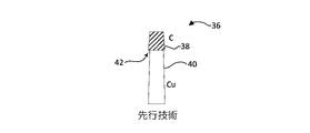
図4および図5は、極めて薄い試料を作製する際の問題の例を示す。図4に示されているように、薄片試料30の断面は、硬いダイヤモンド基板34上に付着させた軟らかいPtキャップ32を有するように作製されている。必要な厚さまで薄くすることによって薄片30を作製すると、この硬さの不一致の結果、より軟らかいPtキャップ32の方が、より硬いダイヤモンド基板34よりも速く侵食される。基板34が十分に薄くなる前に保護キャップ32は完全に消耗すると思われるため、この組合せは、ユーザが、薄片を所望どおりに薄くすることを妨げるであろう。反対に、図5に示されているように、薄片試料36の断面は、軟らかい銅基板40上に置かれた硬い炭素キャップ38を有するように作製されている。この例では、アンダーカッティング42が観察されることがある。より軟らかい基板40の方がより硬いキャップ38よりも速く消耗するためである。これによって薄片が早期に破損することがあり、「カーテニング」などの断面切削表面アーチファクトが生じることもある。
4 and 5 show examples of problems in making extremely thin samples. As shown in FIG. 4, the cross section of the
カーテニングは、試料の表面をさざ波状にしまたはでこぼこにするアーチファクトである。カーテニングはさまざまな理由から生じる。試料が、均質でなく、異なるスパッタリング速度を有する異なる材料からなる場合には、より硬い材料が、断面切削面からわずかに突き出た抵抗性のエリアを形成することがある。それらの突出部は、それらの突出部の下方の領域を隠し、下方へ伝搬する垂直の筋を作る。図6は、シリコン基板を有する試料44を示し、タングステン保護層がカーテニングを示している。「カーテン」ができるのは、タングステンがシリコン基板よりも硬く、イオン・ビームによるスパッタリングに対してより抵抗性があるためである。これによって、基板の断面切削面からわずかに突き出た特徴部分が生じる。このより硬い張り出したタングステンは基本的に、その直下の基板を隠し、タングステンの垂直な突出部を残す。あるいは、硬いいくつかのキャッピング材料は、たとえキャッピング材料自体が内部的に均質である場合でも、イオン・ビームにさらされたときに、さざ波のようなパターンまたは直線で構成されたパターンを形成する。図7は、シリコン基板を有する試料46を示し、炭素保護層がカーテニングを示している。断面ミリングが実行されたとき、この炭素層の材料は徐々に、テクスチャが非常に粗い表面を示すようなる。このように、この例では炭素層の構造がカーテニングにつながる。これらのタイプの構造変動または密度変動を有する試料を上から下へ向かって薄くすることによって、垂直な隆起線または変動が、試料の最上部(最上部はイオン・ビーム源に最も近いと定義される)の近くのより高密度の材料(すなわち金属線)から、イオン・ビームの方向に対して平行な方向に走る断面切削面に沿って、下方へ伝搬する。カーテニングは、低いスパッタリング率を有する材料のパターン形成された多数の層がより高いスパッタリング率を有する材料を遮っている半導体材料中で最も頻繁に観察される。カーテニングは、スパッタリング率の変化がミリング入射角とともに変化する異なる構造領域を示す材料中でも観察されることがある。空隙を有する試料もカーテンを誘起する。カーテニング・アーチファクトは、TEM画像化の質を低下させ、最小有効供試体厚さを制限する。
Cartening is an artifact that makes the surface of a sample rippling or bumpy. Cartening arises for a variety of reasons. If the sample is not homogeneous and consists of different materials with different sputtering rates, the harder material may form a resistant area slightly protruding from the cross-section cutting surface. Those protrusions hide the area below those protrusions and create vertical streaks that propagate downwards. FIG. 6 shows a
別のタイプのアーチファクトは「ゴルフ・ティー(golf tee)」と呼ばれている。例えば、試料上の関心の領域の上のタングステン層または炭素層であり、通常はシリコンなどの材料である。このキャッピング材料とシリコン基板は異なる「硬さ」(イオン・ビームによるスパッタリングに対する抵抗性)を有し、その結果、「ゴルフ・ティー」と呼ばれる最上部から最下部への厚さの変動が生じる。ゴルフ・ティーでは、試料の厚さが最上部でより大きく、それより下ではより薄い寸法になり、そのため、Y断面で観察したときに試料が「ゴルフ・ティー」の輪郭を有する。関心の領域は普通、薄片の上面の近くに含まれるため、より厚いこの寸法が、関心の領域を不明瞭にし、TEMで観察するのに決して望ましくない試料を生じさせることがある。 Another type of artifact is called a "golf tee". For example, a tungsten layer or carbon layer above the area of interest on the sample, usually a material such as silicon. The capping material and the silicon substrate have different "hardness" (resistance to sputtering by an ion beam), resulting in a thickness variation from the top to the bottom called a "golf tee". In a golf tee, the sample is thicker at the top and thinner below it, so that the sample has a "golf tee" contour when viewed in Y section. Since the area of interest is usually contained near the top surface of the flakes, this thicker dimension can obscure the area of interest and give rise to a sample that is never desirable for TEM observation.
「ゴルフ・ティー」現象の一例が図8に示されている。図8は、イオン・ビーム誘起付着(IBID)タングステン保護層52が上面に位置するTEM試料50を示す。この例では、薄くした後、保護層52の直下の試料50の幅が44nmであり、保護層52の下150nmのところではそれが25nmまで狭くなっている。この厚さの変動は、シリコン基板とタングステン保護層との間のエッチング速度の差の結果である。タングステンは、シリコンよりも硬く、シリコンよりも高密度の材料であり、かなり低いエッチング速度を有する。それによって、タングステン保護層52の幅が薄片本体の幅よりも広くなる。関心の領域は通常、関心の領域を不明瞭にしまたは関心の領域をTEMで観察することを妨げる「ゴルフ・ティー」が生じる一般的なエリアに位置する。
An example of the "golf tee" phenomenon is shown in FIG. FIG. 8 shows a
表面アーチファクトおよび勾配変化のない制御された加工物表面を得るための改良された材料付着法が求められている。 There is a need for improved material attachment methods to obtain controlled workpiece surfaces without surface artifacts and gradient changes.
本発明の目的は、観察のために関心のエリアを露出させる荷電粒子ビーム処理のための保護層を形成する改良された方法および装置を提供することにある。 It is an object of the present invention to provide an improved method and apparatus for forming a protective layer for charged particle beam processing that exposes an area of interest for observation.
加工物を荷電粒子ビーム処理して、観察のために関心の領域を露出させるシステムは、加工物の表面に前駆体ガスを供給し、基板に向かって荷電粒子ビームを導いて、前駆体ガスから関心の領域の上で保護層の付着を誘起し、基板に向かって荷電粒子ビームを導いて、保護層を貫通するようにミリングし、それによって保護層の下方の関心の領域を露出させる方法および装置を含む。保護層は、異なるスパッタリング速度を有する少なくとも2種類の異なる材料からなる。 A system that processes a workpiece with a charged particle beam to expose an area of interest for observation supplies a precursor gas to the surface of the workpiece and guides the charged particle beam towards the substrate from the precursor gas. A method of inducing adhesion of the protective layer over the area of interest, directing a charged particle beam towards the substrate and milling through the protective layer, thereby exposing the area of interest below the protective layer and Includes equipment. The protective layer consists of at least two different materials with different sputtering rates.
以上では、以下の本発明の詳細な説明をより十分に理解できるように、本発明の特徴および技術上の利点をかなりおおまかに概説した。以下では、本発明の追加の特徴および追加の利点を説明する。開示される着想および特定の実施形態を、本発明の同じ目的を達成するために他の構造体を変更しまたは設計するためのベースとして容易に利用することができることを当業者は理解すべきである。さらに、このような等価の構造体は、添付の特許請求の範囲に記載された本発明の範囲を逸脱しないことを当業者は理解すべきである。 In the above, the features and technical advantages of the present invention have been outlined fairly roughly so that the following detailed description of the present invention can be more fully understood. The following describes additional features and advantages of the present invention. Those skilled in the art should understand that the disclosed ideas and specific embodiments can be readily utilized as a basis for modifying or designing other structures to achieve the same object of the invention. be. Moreover, those skilled in the art should understand that such equivalent structures do not deviate from the scope of the invention described in the appended claims.
本特許書類または出願書類は、カラーで作成された少なくとも1つの図面を含む。カラー図面を含む本特許または特許出願公開の複写物は、請求および必要な料金の支払いの後に特許庁によって提供される。次に、本発明および本発明の利点のより完全な理解のため、添付図面とともに読まれる以下の説明を参照する。 The patent or application documents include at least one drawing made in color. A copy of this patent or published patent application, including color drawings, will be provided by the Patent Office after requesting and paying the required fees. Next, for a more complete understanding of the present invention and the advantages of the present invention, the following description read with the accompanying drawings will be referred to.
本発明の実施形態は、異なる2種類の材料を使用して保護層を形成することにより、荷電粒子ビーム処理のための改良された保護層を提供する。 Embodiments of the present invention provide an improved protective layer for charged particle beam processing by forming a protective layer using two different materials.
一実施形態によれば、材料付着を実行して、基板材料のスパッタリング速度と実質的に一致したスパッタリング速度を有する保護材料層を提供する。FIBシステムの真空室内で基板に向かって荷電粒子ビームを導いて、前駆体ガス混合物からの材料付着を誘起する。ガス混合物成分の比率を変化させることによって、スパッタリングに対する保護層材料付着物の抵抗性を調節することができる。試料基板の材料に応じて保護層材料の硬さを変化させるため、前駆体の比率を幅広い範囲にわたって変化させることができる可変の流量制御能力および混合能力を有する多ガス注入システムを使用する。 According to one embodiment, material attachment is performed to provide a protective material layer having a sputtering rate substantially consistent with the sputtering rate of the substrate material. A charged particle beam is guided towards the substrate in the vacuum chamber of the FIB system to induce material adhesion from the precursor gas mixture. By varying the proportion of gas mixture components, the resistance of the protective layer material deposits to sputtering can be adjusted. To vary the hardness of the protective layer material depending on the material of the sample substrate, a multi-gas injection system with variable flow control and mixing capabilities capable of varying the ratio of precursors over a wide range is used.
他の実施形態によれば、材料付着を実行して、異なるエッチング速度をそれぞれが有する複数の層として付着させた2種類以上の材料組成物を含む保護層を提供する。FIBシステムの真空室内で基板に向かって荷電粒子ビームを導いて、前駆体ガスから関心の領域の上方の試料基板上への第1の保護層の付着を誘起することが好ましい。次いで、試料基板に向かってイオン・ビームを導いて、前駆体ガスから第1の保護層の上への少なくとも1つの第2の保護層の付着を誘起する。第1の保護層が、試料のエッチング速度と厳密に一致したエッチング速度を有し、第2の保護層(および他の一切の層)が、試料のエッチング速度とは異なるエッチング速度を有することが好ましい。例えば、より軟らかい基板に対しては、最初に、より軟らかい保護材料を、基板と直接に接触するように付着させ、次いで、この第1の層の上に、より硬い第2の層を付着させることができる。より硬い層は、イオン・ビームによる侵食に抵抗し、より軟らかい最下層は、断面切削アーチファクトを防ぐ。基板のスパッタリング速度と厳密に一致したスパッタリング速度を有する最下層は、断面切削アーチファクトの危険を低下させる。ダイヤモンド、炭素、炭化シリコンなどのより硬い基板に対しては、最初に、より硬い保護層を、基板と直接に接触するように付着させ、この第1の層の上に、より軟らかい材料層を付着させることができる。 According to another embodiment, material attachment is performed to provide a protective layer containing two or more material compositions attached as a plurality of layers, each having a different etching rate. It is preferred to guide a charged particle beam towards the substrate in the vacuum chamber of the FIB system to induce adhesion of the first protective layer from the precursor gas onto the sample substrate above the region of interest. An ion beam is then directed towards the sample substrate to induce attachment of at least one second protective layer from the precursor gas onto the first protective layer. The first protective layer may have an etching rate that closely matches the etching rate of the sample, and the second protective layer (and any other layer) may have an etching rate that is different from the etching rate of the sample. preferable. For example, for a softer substrate, a softer protective material is first attached to the substrate in direct contact, and then a harder second layer is attached onto the first layer. be able to. The harder layer resists erosion by the ion beam, and the softer bottom layer prevents cross-section cutting artifacts. The bottom layer, which has a sputtering rate that closely matches the sputtering rate of the substrate, reduces the risk of cross-section cutting artifacts. For harder substrates such as diamond, carbon, and silicon carbide, a harder protective layer is first attached in direct contact with the substrate, and a softer material layer is placed on top of this first layer. Can be attached.
他の実施形態では、材料付着を実行して、保護層を形成する、互層をなす複数の材料層を提供する。この保護層では、互層をなす薄い材料層を別々のガス・ケミストリを使用して付着させることによって、保護層材料のエッチング速度が「調整されて」おり、この保護層は、個々の成分のエッチング速度とエッチング速度の間のエッチング速度を有する交互に「パフェ状」のマクロ構造を形成する。個々の成分の厚さおよび層の総数を調節することによって、ユーザは、所望の膜特性を達成するある程度の調整可能性を達成することができる。互層をなす極めて薄い無数の層を限界まで付着させることができ、その結果、付着物は複合混合物に似たものになる。 In another embodiment, a plurality of alternating layers of material are provided that perform material adhesion to form a protective layer. In this protective layer, the etching rate of the protective layer material is "adjusted" by attaching alternating thin material layers using separate gas chemistries, and this protective layer etches the individual components. Alternately form "parfait-like" macrostructures with etching velocities between velocities and etching velocities. By adjusting the thickness of the individual components and the total number of layers, the user can achieve some degree of adjustability to achieve the desired membrane properties. A myriad of very thin alternating layers can be attached to the limit, resulting in a deposit resembling a complex mixture.
他の実施形態では、ガス前駆体の混合物を使用して材料を付着させるが、付着の進行中にガスの比率を徐々に調節して、複合キャッピング材料を形成する。この複合キャッピング材料は、保護層の最下部が主に1つの成分からなり、保護層の最上部が主に別の成分からなり、中間領域が中間の組成を有するような態様で形成される。このような調節は、保護材料内へミリングが進むにときに、硬から軟(または軟から硬)への緩やかな遷移を提供する。 In another embodiment, a mixture of gas precursors is used to attach the material, but the proportion of gas is gradually adjusted during the course of attachment to form a composite capping material. The composite capping material is formed in such a manner that the bottom of the protective layer is mainly composed of one component, the top of the protective layer is mainly composed of another component, and the intermediate region has an intermediate composition. Such adjustments provide a gradual transition from hard to soft (or soft to hard) as the milling progresses into the protective material.
他の実施形態では、TEM薄片の作製で、ビームの後部による侵食に起因する薄片の破損を防ぐように犠牲保護キャップの硬さを調整するために、本明細書に記載された材料付着法を実行することができ、それらの材料付着法は、カーテニングや界面における側壁の勾配変化などの断面切削アーチファクトを最小化することができる。 In another embodiment, in the production of TEM flakes, the material attachment method described herein is used to adjust the hardness of the sacrificial protective cap to prevent flaking of the flakes due to erosion by the rear of the beam. These material attachment methods can be performed and can minimize cross-section cutting artifacts such as cartening and gradient changes of the sidewalls at the interface.
他の実施形態では、欠陥および勾配変化のない切削面を有する一般的な片面FIB断面を複合キャッピング層を使用して形成する用途で、本明細書に記載された材料付着法を実行することができる。 In another embodiment, the material attachment method described herein can be performed in applications where a common single-sided FIB cross section with a cut surface without defects and gradient changes is formed using a composite capping layer. can.
他の実施形態では、複合付着膜を使用して、イオン・ビーム・ミリングを用いて形成された(バイアなどの)高アスペクト比構造体のミリング後の外形を制御することができる用途で、本明細書に記載された材料付着法を実行することができる。 In another embodiment, the composite attachment membrane can be used to control the post-milling profile of high aspect ratio structures (such as vias) formed using ion beam milling. The material attachment method described in the specification can be carried out.
本発明の好ましい第1の実施形態によれば、FIBカラムとSEMカラムの両方を有するデュアル・ビームFIB/SEMシステム内に、半導体ウェーハなどの基板を装填する。デュアル・ビーム・システムについて論じるが、他のFIBシステムを使用して本発明を実施することもできることを理解すべきである。ウェーハは、手動で移送することができ、または、好ましくは、多ウェーハ・キャリアおよび自動装填ロボット(図示せず)によって移送する。 According to the preferred first embodiment of the present invention, a substrate such as a semiconductor wafer is loaded in a dual beam FIB / SEM system having both a FIB column and an SEM column. Although the dual beam system is discussed, it should be understood that the present invention can also be practiced using other FIB systems. Wafers can be transferred manually, or preferably by a multi-wafer carrier and an autoloading robot (not shown).
薄片試料を作製する用途では、抜き取って分析する関心の特徴部分を含む試料上の領域の位置(すなわち薄片部位)を決定する。例えば、基板は、半導体ウェーハまたは半導体ウェーハの一部とすることができ、抜き取る試料は、TEMを使用して観察する集積回路の一部を含むことができる。通常は、ウェーハ上もしくはウェーハ片上の基準マークの位置をマシン・ビジョンを使用して突き止めることによって、または、パターンが形成されていないウェーハの縁および位置合せノッチもしくはフラットを使用することによって、粗く基板の位置合せをする。あるいは、画像認識ソフトウェアを使用して薄片部位の位置を自動的に突き止めてもよい。適当な画像認識ソフトウェアは、米マサチューセッツ州NatickのCognex Corporationから入手可能である。同様の特徴部分のサンプル画像を使用することによって、またはCADデータからの幾何学的情報を使用することによって所望の薄片位置を突き止めるように、画像認識ソフトウェアを「学習させる」ことができる。自動化されたFIBまたはSEM計測を使用して、薄片部位を識別し、または薄片部位の識別を支援することもできる。計測は、画像ベースのパターン認識、エッジ・ファインディング、ADR、質量中心計算またはブロブ解析からなることができる。所望ならば、精密で正確な位置検出マークとして、基板表面に基準マークをミリングすることができる。 In applications that produce flaky samples, the location of the region on the sample (ie, the flaky site) that contains the feature portion of interest to be sampled and analyzed is determined. For example, the substrate can be a semiconductor wafer or part of a semiconductor wafer, and the sample to be sampled can include part of an integrated circuit to be observed using TEM. Rough substrates, typically by locating reference marks on wafers or wafer pieces using machine vision, or by using unpatterned wafer edges and alignment notches or flats. Align. Alternatively, image recognition software may be used to automatically locate the flakes. Suitable image recognition software is available from Cognex Corporation in Natick, Massachusetts, USA. Image recognition software can be "trained" to locate the desired flakes position by using sample images of similar feature portions or by using geometric information from CAD data. Automated FIB or SEM measurements can also be used to identify flaky areas or assist in identifying flaky areas. The measurement can consist of image-based pattern recognition, edge finding, ADR, mass center calculation or blob analysis. If desired, the reference mark can be milled on the surface of the substrate as a precise and accurate position detection mark.
次いで、この薄片部位の上に、試料を保護する複合保護層を付着させる。好ましい第1の実施形態では、2種類以上の前駆体ガスが同時に流れる多ガス注入システムを使用して、IBIDまたはEBID付着を実行することができる。例えば、付着させた材料が2種類の個々の成分の中間の特性を有する付着を実行することができる。例えば、Pt前駆体とC前駆体の混合物を用いて達成されるIBID付着を実行して、Pt前駆体およびC前駆体を個々に用いて得られる特性の中間の特性を有する保護層を得ることができる。前駆体の混合は多くの方法で実行することができる。例えば、個々の化学前駆体を含む2つ以上の容器が単一のガス・ノズル出口を共用し、化学前駆体容器と出口の間に位置するパルス弁によって、個々の成分の相対流量を制御することができる。 Next, a composite protective layer that protects the sample is attached onto the flaky portion. In a preferred first embodiment, a multigas injection system in which two or more precursor gases flow simultaneously can be used to perform IBID or EBID attachment. For example, the adhered material can perform the adhesion having properties intermediate between the two individual components. For example, IBID adhesion achieved with a mixture of Pt and C precursors is performed to obtain a protective layer with properties intermediate between those obtained with the Pt and C precursors individually. Can be done. Mixing of precursors can be performed in many ways. For example, two or more vessels containing individual chemical precursors share a single gas nozzle outlet, and a pulse valve located between the chemical precursor vessel and the outlet controls the relative flow rate of the individual components. be able to.
図9は、本発明の一実施形態を含むビーム・システム100の略図を示す。ビーム・システム100は試料真空室102を含み、試料真空室102は、ビーム110によって処理される加工物106を支持する試料ステージ104を含み、ビーム110は、レーザ、荷電粒子ビーム・カラムなどのビーム生成サブシステムによって生成される。例えば、荷電粒子ビーム・カラム112は、荷電粒子源113、1つまたは複数の集束レンズ114および偏向器116を含み、偏向器116は、指定されたパターンに従って加工物表面をビーム110で走査し、または、他の方法で、指定されたパターンに従って加工物表面でビーム110を導く。高真空ターボ・ポンプ120とバッキング・ポンプ122の組合せなどの排気システムが、処理の間、試料真空室102を、好ましくは10-3ミリバール未満、より好ましくは10-4ミリバール未満、よりいっそう好ましくは約10-5ミリバール以下の真空に維持する。バッキング・ポンプ122は排気出口124に排気する。
FIG. 9 shows a schematic diagram of a
多ガス注入システム(MGIS)弁132から延びる後退可能な針130によって、加工物表面の局所領域にガスが供給される。MGIS弁132については後により詳細に説明する。付着前駆体ガス、エッチング前駆体ガス、不活性パージ・ガスなどのガスがガス・リザーバ131に蓄えられている。用語「リザーバ」は、任意のガス源を含むように幅広く使用される。一部のリザーバ131は固体材料または液体材料を含むことができ、それらの固体材料または液体材料は例えばるつぼ(crucible)の中で加熱されて所望のガスを放出し、別のリザーバ131は圧縮ガスを含むことができる。リザーバ131はそれぞれ、対応する導管133によってMGIS弁132に接続されており、それぞれのリザーバ131とMGIS弁132の間の流路には調整弁134および停止弁136がある。図9は、2つのリザーバおよび対応する導管を示しているが、本発明は、いかなる数のリザーバにも限定されない。本発明のいくつかの実施形態は6つ以上のリザーバを使用し、別の実施形態は単一のガス源を使用する。
A
予めセットされたガスの配合が実行されると、MGIS弁132の針130が延ばされ、プロセス・ガスが、弁132から、針130を通って、加工物106の表面の荷電粒子ビーム110が集束する点の近くに流れる。
When the preset gas compounding is performed, the
荷電粒子ビーム110および針130の下に加工物を配置するために試料ステージ104が使用される。針130から注入された試料真空室内のガスは最終的に、ターボ・ポンプ120によって試料真空室から排出される。真空ポンプ138は、MGIS弁の内部に残ったガスを、MGIS真空導管140を通して除去する。MGIS真空導管140はMGIS真空弁142を備える。
A
複合保護層用のこの特定の配合は、試料基板の材料に応じた特定の比率で前駆体を混合することからなる。一方の前駆体が比較的に軟らかい付着材料を生成し、もう一方の前駆体が比較的に硬い付着材料を生成することが好ましい。したがって、ユーザは、付着層の硬さを、それぞれの個々の前駆体の特性間の任意の特性に調整することができる。十分に薄くすることを可能にするため、および界面アーチファクトを防ぐために、これらの前駆体は、保護層材料のスパッタリング速度が基板材料のスパッタリング速度と一致するような比率で混合される。このMGIS送達ハードウェア内の弁のデューティ・サイクルを0%から100%の間で連続的に変化させることができる。したがって、混合された個々の前駆体成分の特性間の中間の特性を有するように、付着材料を調節することができる。これによって、さまざまな基板材料およびさまざまな用途に合わせて付着をカスタマイズすることができる。 This particular formulation for the composite protective layer consists of mixing the precursor in a particular proportion depending on the material of the sample substrate. It is preferred that one precursor produces a relatively soft adhesive material and the other precursor produces a relatively hard adhesive material. Thus, the user can adjust the hardness of the adherent layer to any property between the properties of each individual precursor. To allow for thin enough and to prevent interfacial artifacts, these precursors are mixed in such a proportion that the sputtering rate of the protective layer material matches the sputtering rate of the substrate material. The duty cycle of the valve in this MGIS delivery hardware can be continuously varied from 0% to 100%. Thus, the adherent material can be adjusted to have properties intermediate between the properties of the individual precursor components mixed. This allows the adhesion to be customized for different substrate materials and different applications.
一例では、炭素-白金(C-Pt)保護層を付着させる。C-Pt前駆体を、基板の材料に応じた特定の比率で混合する。これは、図10および図11に示された等値線図に示されているとおりにC-Pt比を調節することによって達成される。図10には、垂直付着成長速度(nm/秒)を、Pt前駆体に対する弁デューティ・サイクル(X軸)およびC前駆体に対する弁デューティ・サイクル(Y軸)の関数として示す等値線図150が示されている。最も高い成長速度が円152によって示されており、PtおよびCの標準単一前駆体材料の成長速度がそれぞれ円154および円156によって示されている。図11には、付着させたC-Pt複合材料のスパッタリング速度を、Pt前駆体に対する弁デューティ・サイクル(X軸)およびC前駆体に対する弁デューティ・サイクル(Y軸)の関数として示す等値線図160が示されている。PtおよびCの標準単一前駆体材料のスパッタリング速度がそれぞれ円162および円164によって示されている。主にCからなる付着物に少量のPtを加えることにより、例えば円166によって示された条件は、保護キャップ層としてどちらの個々の成分よりも優れた材料を付着させる。この層は、Pt単独よりもずっと硬いが、C単独のカーテニング現象を示さない。可変デューティ・サイクル弁制御またはパルス弁の「オン」時間の百分率、および多ガス噴射システムの混合能力が、このような調節を可能にする。このように、図11の等値線図160の左上から右下に移動することによって、所望の「硬さ」を達成することができる。したがって、ユーザは、試料に適合するように、特に試料基板の硬さと一致するように、付着する層の硬さをカスタマイズすることができる。
In one example, a carbon-platinum (C-Pt) protective layer is attached. The C-Pt precursor is mixed in a specific ratio depending on the material of the substrate. This is achieved by adjusting the C-Pt ratio as shown in the contour diagrams shown in FIGS. 10 and 11. FIG. 10 shows the vertical accretion growth rate (nm / sec) as a function of the valve duty cycle (X-axis) for the Pt precursor and the valve duty cycle (Y-axis) for the C precursor. It is shown. The highest growth rates are indicated by
例えば、図12~図14に示されているように、さまざまな硬さ特性を有するC-Pt複合材料を基板上に付着させる。例えば、Cを多く含む複合物を達成するように弁デューティ・サイクルを連続的に調節することによって(Cの弁デューティ・サイクル=80%、Ptの弁デューティ・サイクル<2%)、基板200上にC-Pt複合材料を形成することができ、その結果、図12に示されているように、非常に硬い(しかしC単独の場合ほどには硬くない)保護層202を付着させることができる。図13に示されているように、Ptを多く含む複合物を達成するように弁デューティ・サイクルを連続的に調節することによって(Cの弁デューティ・サイクル<2%、Ptの弁デューティ・サイクル=80%)、基板206上にC-Pt複合材料を形成することができ、その結果、非常に軟らかい(しかしPt単独ほどには軟らかくない)保護層208を付着させることができる。ダイヤモンドなどの硬い基板試料を使用する場合には、ダイヤモンド基板の硬さと厳密に一致した硬さを有するCを多く含む層を付着させることができる。図14に示されている一例のように、80%-5%(C対Pt)のMGIS設定を用いて付着させたC-Pt材料の保護層212を有する基板210の方が、純粋なC前駆体または純粋なPt前駆体を用いて得られた層よりも好ましい。80%-5%の比率は、単独で使用された個々のCまたはPtよりも高い材料成長速度を有する。さらに、この比率は、Ptよりも高いスパッタリング抵抗性を有し、Cよりも少ないカーテニング・アーチファクトを有する。
For example, as shown in FIGS. 12-14, a C-Pt composite material with various hardness properties is adhered onto the substrate. For example, by continuously adjusting the valve duty cycle to achieve a C-rich composite (C valve duty cycle = 80%, Pt valve duty cycle <2%), on
さまざまな硬さ特性を有する基板に対して他の付着物を得ることができる。例えば、中間のデューティ・サイクル(例えば炭素と白金の両方に対して40%)を用いた保護層は、両方の成分を個々に用いて得られる特性のほぼ中間の特性を有する。より軟らかい基板特性を有する有機樹脂などの試料に対しては、Ptに富むように付着前駆体を調節することができる。 Other deposits can be obtained for substrates with various hardness properties. For example, a protective layer with an intermediate duty cycle (eg 40% for both carbon and platinum) has properties approximately intermediate to those obtained with both components individually. For samples such as organic resins with softer substrate properties, the adhesion precursor can be adjusted to be rich in Pt.
可能なデューティ・サイクルと試料の組合せには、中程度の硬さのシリコン基板と50%-50%(C対Pt)の弁デューティ・サイクルを使用した付着層との組合せ、硬いダイヤモンド基板と80%-1%(C対Pt)の弁デューティ・サイクルを使用した付着層との組合せ、および軟らかい樹脂基板と5%-80%(C対Pt)の弁デューティ・サイクルを使用した付着層との組合せなどがある。同様に、従来のMGISシステムを用いて前駆体を混合することもでき、そのようなシステムでは、それぞれの物質のるつぼ温度を制御することによって、前駆体の比率をおおまかに調節することができる。しかしながら、デューティ・サイクルの多くの組合せが可能であり、これらの例は、付着する材料の硬さを、基板材料の硬さと一致するように連続的に変化させることができることを例示するものである。 Possible duty cycle and sample combinations include a medium hardness silicon substrate with an adhering layer using a 50% -50% (C vs. Pt) valve duty cycle, a hard diamond substrate and 80. Combination with a bond layer using a% -1% (C vs. Pt) valve duty cycle, and with a soft resin substrate and a bond layer using a 5% -80% (C to Pt) valve duty cycle. There are combinations and so on. Similarly, precursors can be mixed using conventional MGIS systems, in which the proportion of precursors can be roughly adjusted by controlling the crucible temperature of each substance. However, many combinations of duty cycles are possible, and these examples illustrate that the hardness of the adhered material can be continuously varied to match the hardness of the substrate material. ..
上述のパルス弁混合手法だけでなく、他の前駆体送達方法を使用することもできる。例えば、質量流量制御弁、ニードル絞り弁を用いて、または、単純に、前駆体の容器の温度を調節してその成分の蒸気圧を調節することによって、個々の前駆体成分の相対流量を調節することもできる。さまざまなサイズのオリフィス(絞り)を使用することによって、またはさまざまな内径を有する管を使用することによって、流量に影響を及ぼすこともできる。最後に、単一の弁を開くと前駆体ガスの混合物が機器の真空室に入るような態様で、多数の前駆体化学物質を同じ容器内で混合することも可能である。多成分前駆体混合物を送達するのに使用する送達手法、および混合物を作るハードウェアまたはシステムに関係なく、前駆体混合物を使用して、付着する材料層の特性を調整することができる。 In addition to the pulse valve mixing method described above, other precursor delivery methods can also be used. Adjusting the relative flow rate of individual precursor components, for example, using a mass flow control valve, a needle throttle valve, or simply by adjusting the temperature of the precursor vessel to regulate the vapor pressure of that component. You can also do it. Flow rates can also be affected by using different sizes of orifices (throttles) or by using tubes with different inner diameters. Finally, it is also possible to mix multiple precursor chemicals in the same container in such a manner that opening a single valve allows the mixture of precursor gases to enter the vacuum chamber of the instrument. Regardless of the delivery method used to deliver the multi-component precursor mixture and the hardware or system that makes the mixture, the precursor mixture can be used to adjust the properties of the material layer to which it adheres.
異なるさまざまな用途に対して、前駆体混合物からの付着材料層を使用することができる。TEM薄片の作製では、犠牲保護キャップの硬さを調整することによって、ビームの後部による侵食に起因する薄片の破損を防ぐことができ、カーテニング、ゴルフ・ティー、界面における側壁の勾配変化などの断面切削アーチファクトを最小化することができる。複合材料付着の他の用途は、欠陥および勾配変化のない切削面を有する一般的な片面FIB断面の形成に使用する用途である。 Adhesive material layers from precursor mixtures can be used for a variety of different applications. In the production of TEM flakes, the hardness of the sacrificial protective cap can be adjusted to prevent flaking of the flakes due to erosion by the rear of the beam, resulting in cross-sections such as cartening, golf tees, and side wall gradient changes at the interface. Cutting artifacts can be minimized. Another use for composite adhesion is for the formation of common single-sided FIB cross sections with cut surfaces without defects and gradient changes.
複合付着層を使用して、イオン・ビーム・ミリングを用いて形成された(バイアなどの)高アスペクト比構造体のミリング後の外形を制御することもできる。これは、FIBナノファブリケーションおよびFIBマイクロファブリケーションに対して、またはイオンビーム・リソグラフィ技法に対して有用であることがある。図15に示されたこの用途では、加工物250が、基板254上に付着させた薄い複合付着キャッピング材料252を含む。基板254は、ユーザが、バイア256などの高アスペクト比構造体をその中に形成したいと思っている基板である。この複合付着物用の特定の配合は、その下のターゲット材料よりも「硬く」なるように選択すべきである。初めのうちは、ミリングが進むにつれて、イオン・ビームは、硬い付着層252にだんだんと深く入り込む。このミリングはついに、硬い付着物252とその下の軟らかい基板254の間の界面に到達する。この時点で、その下の基板254がミリングされ始めるが、ミリングされるのは、ミリング速度が最も大きかったイオン・ビームの外形の中心部分だけである。その下の基板254はキャッピング材料252よりも軟らかく、イオン・ビームの外形はほぼガウス分布に従うため、軟らかい材料254は、イオン・ビーム分布の強い中心によって迅速にミリングされるはずであり、一方、強さに劣るイオン・ビームの「後部」は、より硬いキャッピング材料252にまだ侵入していない。
The composite adhesion layer can also be used to control the post-milling profile of high aspect ratio structures (such as vias) formed using ion beam milling. It may be useful for FIB nanofabrication and FIB microfabrication, or for ion beam lithography techniques. In this application shown in FIG. 15, the
したがって、より軟らかいターゲット材料の上により硬いキャッピング膜があるこの配列は、イオン・ミリング・プローブの形状を鋭くする効果を有し、キャップのない基板を用いて達成することが可能であろう寸法よりも細い寸法を有するバイアを得ることが可能である。所望ならば、最終ステップで最上部のキャッピング膜を除去し、「鋭くされた」高アスペクト比ミリングを後に残すことができる。これは例えば、シリコン基板の上に硬い炭素膜を使用することによって達成することができる。この炭素膜は、酸素プラズマ洗浄ステップによって除去することができる。このようにして、比較的に細い寸法および平行な側壁を有する高アスペクト比構造体を形成することができる。 Therefore, this arrangement with a harder capping membrane on top of the softer target material has the effect of sharpening the shape of the ion milling probe and is more than the dimensions that would be possible with a capless substrate. It is also possible to obtain vias with fine dimensions. If desired, the top capping film can be removed in the final step, leaving behind a "sharpened" high aspect ratio milling. This can be achieved, for example, by using a hard carbon film on a silicon substrate. This carbon film can be removed by an oxygen plasma cleaning step. In this way, it is possible to form a high aspect ratio structure with relatively fine dimensions and parallel sidewalls.
他の例では、その下の基板よりも軟らかいキャッピング膜を付着させることによって、(最上部が朝顔形に開いた)面取りされた外形または次第に細くなる外形を有するバイアを形成することができる。図16に示されたこの例では、その下の基板264よりも軟らかいキャッピング層262およびバイア266が形成された加工物260が示されている。軟らかいキャッピング層262に対するビームの後部の効果によってより大きな側方侵食が生じ、その結果、キャップなしでミリングされたバイアに比べて、バイア構造体の最上部が顕著に広がっている。
In another example, a capping film that is softer than the underlying substrate can be attached to form a via with a chamfered outer shape (top open in a morning glory shape) or a progressively thinner outer shape. In this example shown in FIG. 16, the
図17は、FIBミリングされたバイア283がその中に形成された複合層282を有するシリコン基板281を含む加工物試料280の一実施形態を示す。複合層282は、層の最下部から最上部へと変化する「硬さ」を有する。このような複合層は、付着の進行中に個々の前駆体成分のデューティ・サイクルを調節することによって形成することができる。例えば、Ptに富む混合物を用いた付着から始め、付着物が成長するにつれてCに富む混合物へと徐々に移行することによって、軟から硬(最下部から最上部)へと変化するPt-C複合層を付着させることができる。このようなプロセスの弁デューティ・サイクルが、図18のグラフ286によって示されている。
FIG. 17 shows an embodiment of a
図19は、FIBミリングされたバイア293がその中に形成された複合層292を有するシリコン基板291を含む加工物試料290を用いた逆プロセスを示す。複合層292は、層の最下部から最上部へと変化する「硬さ」を有する。このような複合層は、付着の進行中に個々の前駆体成分のデューティ・サイクルを調節することによって形成することができる。例えば、Cに富む混合物を用いた付着から始め、付着物が成長するにつれてPtに富む混合物に徐々に移行することによって、硬から軟(最下部から最上部)へと変化するPt-C複合層を付着させることができる。このようなプロセスの弁デューティ・サイクルが、図20のグラフ296によって示されている。
FIG. 19 shows a reverse process using a workpiece sample 290 containing a
複合層の例としてPt-C混合物を論じたが、他の前駆体の組合せによっても、可変の材料特性を有する付着層を形成することができることを理解すべきである。例えば、ナフタレンからなる前駆体および(メチルシクロペンタジエニル)トリメチル白金からなる前駆体を用いて、炭素-白金複合物を得ることができる。前駆体ナフタレンおよび前駆体W(CO)6を使用して炭素-タングステン複合物を得ることができる。(メチルシクロペンタジエニル)トリメチル白金からなる前駆体およびW(CO)6からなる前駆体を使用して、白金-タングステン複合物を得ることができ、ナフタレンからなる前駆体およびTEOSまたはTMCTSまたはHMCHSからなる前駆体を用いて、炭素-SiOX複合物を得ることができる。 Although the Pt-C mixture was discussed as an example of the composite layer, it should be understood that combinations of other precursors can also form adherent layers with variable material properties. For example, a precursor consisting of naphthalene and a precursor consisting of (methylcyclopentadienyl) trimethyl platinum can be used to obtain a carbon-platinum complex. Precursor naphthalene and precursor W (CO) 6 can be used to obtain a carbon-tungsten composite. Precursors consisting of (methylcyclopentadienyl) trimethylplatinum and precursors consisting of W (CO) 6 can be used to obtain platinum-tungsten complexes, precursors consisting of naphthalene and TEOS or TMCTS or HMCHS. A carbon-SiO X composite can be obtained using a precursor consisting of.
誘電体付着の「硬さ」を調節することが可能であり、それらの付着は通常、シロキサン・ベースの前駆体および酸化剤を用いて実行することができる。酸化剤の濃度が高いと、完全に飽和したSiO2化学量論組成を有する付着層が得られ、酸化剤の量を減らして付着させた層は完全には飽和せず、X<2の化学量論組成SiOXを有する。このような調整には、シロキサン-酸化剤の以下の組合せのうちの任意の組合せが適している:TEOS(オルトケイ酸テトラエチル)とO2、TMCTS(テトラメチルシクロテトラシロキサン)とN2O、およびHMCHS(ヘキサメチルシクロヘキサシロキサン)と水。しかしながら、上記のシロキサンのうちの任意のシロキサンを、上記の酸化剤のうちの任意の酸化剤とともに使用することができる。 It is possible to adjust the "hardness" of the dielectric deposits, which can usually be performed using siloxane-based precursors and oxidants. When the concentration of the oxidant is high, an adherent layer having a completely saturated SiO 2 stoichiometric composition is obtained, and the layer adhered by reducing the amount of the oxidant is not completely saturated, and the chemistry of X <2. It has a stoichiometric composition SiO X. Any combination of the following combinations of siloxane-oxidizers is suitable for such adjustments: TEOS (tetraethyl orthosilicate) and O2 , TMCTS ( tetramethylcyclotetrasiloxane) and N2O, and HMCHS (hexamethylcyclohexasiloxane) and water. However, any siloxane of the above siloxanes can be used with any of the above oxidants.
潜在的には、以下の1次イオンのうちの任意の1次イオンを発生させるプラズマFIB機器を、前駆体シロキサンとともに使用して、可変の硬さを有する誘電層を付着させることができる:O+、O2 +、O3 +、N+、N2 +、H2O+、H2O2 +、N2O+、NO+、NO2 +。この場合には、これらの1次ビーム種自体が酸化剤である。したがって、付着プロセス中にビーム電流密度、前駆体流量および/またはイオン・ビーム・エネルギーを調節することによって、完全に飽和したSiO2化学量論組成から、より飽和度が低いSiOX(X<2)化学量論組成までの範囲にわたる付着層を形成することができる。 Potentially, a plasma FIB instrument that generates any of the following primary ions can be used with the precursor siloxane to attach a dielectric layer with variable hardness: O. + , O 2 + , O 3 + , N + , N 2 + , H 2 O + , H 2 O 2 + , N 2 O + , NO + , NO 2 + . In this case, these primary beam species themselves are oxidants. Therefore, by adjusting the beam current density, precursor flow rate and / or ion beam energy during the adhesion process, the fully saturated SiO 2 stoichiometric composition will be less saturated SiO X (X <2). ) It is possible to form an adhesion layer ranging from stoichiometric composition.
上記の例では、材料の「硬さ」またはイオン・ビームによるスパッタリングに対する抵抗性を調整することを論じたが、同じ方法を使用して他の材料特性を調節することもできることを理解すべきである。例えば、誘電膜の抵抗率は、酸化剤の濃度が増大するにつれて増大する。したがって、シロキサン-酸化剤混合物を制御することによって、ユーザは、より大きな導電率を有する膜またはより小さな導電率を有する膜を付着させることができる。前駆体の混合によって調整されうる他の特性は、付着膜の光学的透明度である。さらに、レーザ支援前駆体分解によって、または加熱された表面での熱分解によって、開示された方法を使用した材料付着を達成することができる。 In the above example, we have discussed adjusting the "hardness" of a material or its resistance to sputtering by an ion beam, but it should be understood that the same method can be used to adjust other material properties. be. For example, the resistivity of a dielectric film increases as the concentration of oxidant increases. Therefore, by controlling the siloxane-oxidant mixture, the user can attach a film with a higher conductivity or a film with a lower conductivity. Another property that can be adjusted by mixing the precursors is the optical transparency of the adherent membrane. In addition, material adhesion using the disclosed methods can be achieved by laser-assisted precursor decomposition or by thermal decomposition on heated surfaces.
本発明の好ましい第2の実施形態によれば、FIBカラムとSEMカラムの両方を有するデュアル・ビームFIB/SEMシステム内に、半導体ウェーハなどの基板を装填する。典型的なデュアル・ビーム・システム構成は、垂直軸を有する電子カラムと、垂直に対して(普通は約52度の傾きで)傾いた軸を有するイオン・カラムとを含む。そのような1つのシステムが、本発明の譲受人である米オレゴン州HillsboroのFEI Companyから市販されているDualBeam(商標)SystemのHeliosファミリーである。 According to a preferred second embodiment of the present invention, a substrate such as a semiconductor wafer is loaded in a dual beam FIB / SEM system having both a FIB column and an SEM column. A typical dual beam system configuration includes an electronic column with a vertical axis and an ion column with an axis tilted with respect to the vertical (usually at an inclination of about 52 degrees). One such system is the Helios family of DualBeam ™ System marketed by FEI Company in Hillsboro, Oregon, USA, the transferee of the invention.
図21は、本発明を実施するのに適した典型的なデュアル・ビームFIB/SEMシステム2110を示す。システム2110は、上ネック部2112を有する排気されたエンベロープを含む。上ネック部2112には、液体金属イオン源2114または他のイオン源および集束カラム2116が位置する。マルチカスププラズマ源または他のプラズマ源などの他のタイプのイオン源、および整形ビーム・カラムなどの他の光学カラム、ならびに電子ビーム・システムおよびレーザ・システムを使用することもできる。
FIG. 21 shows a typical dual beam FIB /
液体金属イオン源2114を出たイオン・ビーム2118は、イオン・ビーム集束カラム2116内を通り、偏向板2120のところに概略的に示された静電偏向手段間を通り抜けて、下室2126内のステージ2124上に配置された例えば半導体デバイスを含む基板または加工物2122に向かって進む。ステージ2124はさらに、1つまたは複数のTEM試料ホルダを支持することができ、そのため、半導体デバイスから試料を抜き取り、それをTEM試料ホルダへ移動させることができる。ステージ2124は、水平面(X軸およびY軸)内で移動することができ、かつ垂直に(Z軸)移動することができることが好ましい。いくつかのシステムでは、ステージ2124がさらに約60度傾くことができ、Z軸を軸にして回転することができる。システム・コントローラ2119は、FIBシステム2110のさまざまな部分の動作を制御する。従来のユーザ・インタフェース(図示せず)にコマンドを入力することにより、ユーザは、システム・コントローラ2119を介して、イオン・ビーム2118で所望の通りに走査することができる。あるいは、システム・コントローラ2119は、RAM、ROM、磁気ディスク、光学ディスクなどのコンピュータ可読記憶装置に記憶されたプログラムされた命令に従って、FIBシステム2110を制御することができる。この記憶装置は、上述の方法を自動的にまたは半自動的に実行するための命令を記憶することができる。SEMからの画像をソフトウェアによって認識して、処理を継続すべきとき、処理を停止すべきとき、およびミリングのためにビームを配置する位置を決定することができる。
The
例えば、ユーザが、ポインティング・デバイスを使用して表示画面上で関心の領域の輪郭を描き、次いで、システムが、後述するステップを自動的に実行して、試料を抜き取ることができる。関心の領域を自動的に識別するため、いくつかの実施形態では、FIBシステム2110が、米マサチューセッツ州NatickのCognex Corporationから市販されているソフトウェアなどの画像認識ソフトウェアを含む。システムは、次いで、本発明に従って試料を手動でまたは自動的に抜き取ることができる。例えば、システムは、多数のデバイスを含む半導体ウェーハ上で類似した特徴部分の位置を自動的に突き止め、異なる(または同じ)デバイス上でそれらの特徴部分の試料を採取することができる。
For example, a user can use a pointing device to outline an area of interest on a display screen, and then the system can automatically perform the steps described below to extract a sample. To automatically identify areas of interest, in some embodiments, the
上ネック部2112を排気するためにイオン・ポンプ2128が使用される。下室2126は、真空コントローラ2132の制御の下、ターボ分子および機械ポンピング・システム2130によって排気される。この真空システムは、下室2126に、約1×10⁻⁷トル(1.3×10⁻⁷ミリバール)から5×10⁻⁴トル(6.7×10⁻⁴ミリバール)の間の真空を提供する。付着前駆体ガスに関しては、またはエッチング支援ガスもしくはエッチング遅延ガスを使用する場合には、室のバックグラウンド圧力は典型的には約1×10⁻⁵トル(1.3×10⁻⁵ミリバール)まで上昇することがある。
An
液体金属イオン源2114と、約1keVから60keVのイオン・ビーム2118を形成しそれを試料に向かって導くイオン・ビーム集束カラム2116内の適当な電極とに高電圧電源2134が接続されている。パターン発生器2138によって提供される所定のパターンに従って動作する偏向コントローラおよび増幅器2136が偏向板2120に結合されており、それによって、パターン発生器2138によって提供されたイオン・ビーム2118が偏向板2120に結合され、それによって、対応するパターンを加工物2122の上面に描くようにイオン・ビーム2118を手動または自動で制御することができる。いくつかのシステムでは、当技術分野ではよく知られているように、偏向板が、最後のレンズの前に置かれる。イオン・ビーム集束カラム2116内のビーム・ブランキング電極(図示せず)は、ブランキング・コントローラ(図示せず)がブランキング電極にブランキング電圧を印加したときに、イオン・ビーム2118を、ターゲット2122ではなくブランキング絞り(図示せず)に衝突させる。
A high
液体金属イオン源2114は通常、ガリウムの金属イオン・ビームを提供する。イオン・ミリング、強化されたエッチングもしくは材料付着によって加工物2122を改変するため、または加工物2122を画像化するために、この源を通常、加工物2122の位置における幅が1/10マイクロメートル未満のビームに集束させることができる。所望ならば、ビデオ回路2142に接続された荷電粒子検出器2140を使用して、2次イオンまたは電子の放出を検出することができる。ビデオ回路2142は、ビデオ・モニタ2144に駆動信号を供給し、コントローラ2119から偏向信号を受け取る。
The liquid
下室2126内における荷電粒子検出器2140の位置は実施形態によって変更することができる。例えば、荷電粒子検出器2140はイオン・ビームと同軸とすることができ、イオン・ビームが通り抜けることを可能にする穴を含むことができる。他の実施形態では、最終レンズを通過し、次いで軸から逸れた2次粒子を集めることができる。任意選択で、FIBシステム2110に、走査電子顕微鏡(SEM)2141およびその電源および制御装置2145が提供される。
The position of the charged
ガス蒸気を導入し加工物2122に向かって導くためにガス送達システム2146が下室2126内へ延びている。本発明の譲受人に譲渡されたCasella他の「Gas Delivery Systems for Particle Beam Processing」という名称の米国特許第5,851,413号明細書は適当なガス送達システム2146を記載している。別のガス送達システムが、やはり本発明の譲受人に譲渡されたRasmussenの「Gas Injection System」という名称の米国特許第5,435,850号明細書に記載されている。例えば、エッチングを強化するためにヨウ素を送達すること、または金属を付着させるために金属有機化合物を送達することができる。
A
本発明の譲受人である米オレゴン州HillsboroのFEIのEasyLiftマイクロマニピュレータなどのマイクロマニピュレータ2147は、真空室内の物体を精確に移動させることができる。真空室内に配置された部分2149のX、Y、Zおよびθ制御を提供するため、マイクロマニピュレータ2147は、真空室の外側に配置された精密電動機2148を備えることができる。小さな物体を操作するため、マイクロマニピュレータ2147に別のエンド・エフェクタを取り付けることができる。後述する実施形態では、このエンド・エフェクタが細いプローブ2150である。この薄いプローブ2150をシステム・コントローラ2119に電気的に接続してプローブ2150に電荷を与え、それによって試料とプローブの間の引力を制御することができる。
A
X-Yステージ2124上に加工物2122を挿入するため、および内部ガス供給リザーバが使用される場合にはリザーバの整備作業のために、扉2160が開かれる。X-Yステージ2124は加熱または冷却することができる。システムが真空状態にある場合に開かないように、この扉はインタロックされている。いくつかの実施形態では、大気圧ウェーハ・ハンドリング・システムが利用される。イオン・ビーム2118にエネルギーを与え集束させるため、高電圧電源が、イオン・ビーム集束カラム2116内の電極に適当な加速電圧を印加する。イオン・ビーム2118が加工物2122に当たると、材料がスパッタリングされる。すなわち試料から材料が物理的に追い出される。あるいは、イオン・ビーム2118が前駆体ガスを分解して、材料を付着させることもできる。集束イオン・ビーム・システムは例えば、本発明の譲受人である米オレゴン州HillsboroのFEI Companyから市販されている。適当なハードウェアの一例を上に示したが、本発明は、特定のタイプのハードウェアで実現されることだけに限定されない。
この実施形態では、2つ以上の異なる層からなる保護キャッピング材料を形成することにより、材料付着を実行することができる。ユーザは、最初に「より軟らかい」材料を、その下の基板と直接に接触するように付着させることを選択することができ、次いで、この第1の層の上に「より硬い」第2の層を付着させることができる。より硬い最上層は、イオン・ビームによる侵食に抵抗し、より軟らかい最下層は、断面切削アーチファクトを防ぐ。具体的には、その下の材料のスパッタリング速度と一致するように最下層を選択することができる場合、断面切削アーチファクトの危険を最小化することができる。別のケースでは順序を逆にすることができる。すなわち、最初により硬い材料を付着させ、続いてより軟らかい材料を付着させることができる。ダイヤモンド、炭素、炭化シリコンなどの硬い材料をFIBミリングするときには、この配列の方が好ましいことがある。 In this embodiment, material adhesion can be performed by forming a protective capping material consisting of two or more different layers. The user can choose to first attach a "softer" material in direct contact with the underlying substrate, and then on top of this first layer a "harder" second. Layers can be attached. The harder top layer resists erosion by ion beams, and the softer bottom layer prevents cross-section cutting artifacts. Specifically, the risk of cross-section cutting artifacts can be minimized if the bottom layer can be selected to match the sputtering rate of the material beneath it. In other cases the order can be reversed. That is, a harder material can be attached first, followed by a softer material. This arrangement may be preferred when FIB milling hard materials such as diamond, carbon, and silicon carbide.
例えば、図22に示されているように、薄片基板1200は保護材料層を有し、この保護材料層は、基板1200の上面の近くの、一般に関心の領域が位置する基板1200の上部領域に対する損傷を防ぐために、最初に、基板1200の上面に、好ましくは電子ビーム誘起付着(EBID)を使用して付着させた最下層1202を有する。代替法は、低エネルギー(<8keV)IBIDを使用する方法であり、この方法も、上面に対する損傷を非常に小さくする。プロセスによってはEBIDよりもむしろ低エネルギーFIB付着が使用される。この最初の最下層材料1202は、特に視射角の作動状態から10-45度外した5kV未満のFIBで、基板1200の材料のエッチング速度とできるだけ一致するように選択される。シリコン(Si)ベースの試料に対しては、この最下層1202が、TEOS(IDEP)、TEOS+H2O(IDEP2)、TEOS+O2、HMCHS、HMCHS+O2(IDEP3)、HMCHS/H2OおよびHMCHS/N2O、TMCTS、TMCTS+O2、および/またはTMCTS/H2O、TMCTS/N2Oなどの一種の酸化シリコン材料であることが好ましい。次いで、イオン・ビーム誘起付着(IBID)を使用して最下層1202の上に最上層材料1204を付着させる。薄片を薄くするプロセス中の保護を提供するため、および試料の外面にアーチファクトが形成されることを防ぐために、最上層材料1204は、基板1200の材料よりも低いエッチング速度を有するように選択される。
For example, as shown in FIG. 22, the
所望ならば、2つ以上の最上層を付着させることができる。この1つまたは複数の最上層はタングステン、炭素または白金であることが好ましい。一例として、炭素は、低kVのFIBミリングに対する優れた抵抗性を有し、このことは保護に寄与するが、その一方で、薄片を反らせる可能性がある重大な内部応力を有する。したがって純粋な炭素層は望ましくない。しかしながら、図23に示されているように、基板1300は、図22に関して論じた層1202と同様の最下材料層1302を含む保護層を有する。厚いタングステン層1306(例えば400nm程度)の上の薄い炭素層1304(例えば30kV処理後の100nmのC層)は、タングステン単独よりも低kV FIB照射に耐え、タングステンは、薄片に剛性を与えると考えられる。薄片側壁に対するFIBビームの角度である35度のかすめ角範囲では、シリコン基板のエッチング速度がタングステンに比べて劇的に増大し、その結果、通常は、薄片の最上部を試料表面から数百nm下の領域よりもずっと厚くするゴルフ・ティー現象が生じる。シリコンおよびタングステンの角度依存スパッタリング速度の定性的な一覧を下表に示す。
Two or more top layers can be attached if desired. The top layer of the one or more is preferably tungsten, carbon or platinum. As an example, carbon has excellent resistance to low kV FIB milling, which contributes to protection, but on the other hand has significant internal stresses that can warp the flakes. Therefore, a pure carbon layer is not desirable. However, as shown in FIG. 23, the
下表1および2は、5kVガリウム・イオンによるスパッタリング率および体積収率を示す。図27Aおよび図27Bには、表1および2のデータをグラフ化したものが示されている。 Tables 1 and 2 below show the sputtering rate and volume yield with 5 kV gallium ions. 27A and 27B show graphs of the data in Tables 1 and 2.


図24は、このような材料付着の一実施形態を示し、この実施形態では、基板1400が、互層をなす材料層1404、1406を含む保護層1402を含み、保護層材料1402のエッチング速度は、互層をなす薄い材料層1404、1406を、別々のガス・ケミストリを使用して付着させることによって「調整されて」おり、保護層1402は、個々の成分のエッチング速度の間のエッチング速度を有する交互に「パフェ状」のマクロ構造を形成する。
FIG. 24 shows one embodiment of such material attachment, in which the
図25は、犠牲保護層1502を有する基板1500の画像を示し、犠牲保護層1502は、基板1500の最上部と保護層1502の間の線引きを目視観察するためのタングステン層1504、SEMによって付着させた酸化シリコンの犠牲層1506、およびタングステンの最上層1508を含む別々の層からなる。見て分かるとおり、薄くした後、犠牲保護層1502内では「ゴルフ・ティー」現象が生じたが、基板1500内では生じなかった。
FIG. 25 shows an image of the
図26は、EBID TEOS層、IBIDタングステン層およびIBID炭素層を含むシリコン薄片を示す。 FIG. 26 shows silicon flakes containing an EBID TEOS layer, an IBID tungsten layer and an IBID carbon layer.
図12~図16の実施形態では、基板試料と同様のエッチング速度を有する犠牲保護層が、ゴルフ・ティーを、上方の保護層内へ移動させ、観察および分析の対象である関心の領域を含む基板の最上部から遠ざける。 In embodiments of FIGS. 12-16, a sacrificial protective layer having an etching rate similar to that of the substrate sample moves the golf tee into the upper protective layer and includes a region of interest that is the subject of observation and analysis. Keep away from the top of the board.
図28に示されているように、本発明は材料付着法を提供する。この方法では、1600で、選択したビーム・システム内に試料を装填する。1602で材料付着のために少なくとも2種類の前駆体ガスを供給する。判断ブロック1604で、材料を異なる層として付着させるのかまたは複合層として付着させるのかを決定する。異なる層を付着させる場合には1606に進み、1608で試料上に第1の層を付着させ、1610で続いて別の層を付着させる。1612で2つの層だけを付着させる場合には、1616で終了すると判断し、1618でプロセスを終える。3つ以上の層を付着させる場合には、1614で終了しないと判断し、プロセスはブロック1608に戻り、1616で終了し、1618でプロセスを終えると決定されるまで、プロセスを続ける。複合層を付着させる場合には1620に進み、1622で決められたレシピに従って少なくとも2種類の前駆体ガスを混合し、1624で試料上に複合層を付着させ、1626でプロセスを終了させる。
As shown in FIG. 28, the present invention provides a material attachment method. In this method, at 1600, the sample is loaded into the selected beam system. At 1602, at least two precursor gases are supplied for material adhesion. The
いくつかの実施形態は、観察のために関心の領域を露出させるために、加工物を荷電粒子ビーム処理する方法であって、
加工物の表面に少なくとも2種類の前駆体ガスを供給することと、
前記少なくとも2種類の前駆体ガスから関心の領域の上方への保護層の付着を誘起するために、基板に向かって荷電粒子ビームを導くこととを含み、保護層が、異なるスパッタリング速度を有する少なくとも2種類の材料からなり、少なくとも2種類の材料が、少なくとも2種類の異なる前駆体ガスの分解によって付着したものであり、この方法がさらに、
保護層を貫通するようにミリングして保護層の下方の関心の領域を露出させるために、基板に向かって荷電粒子ビームを導くこと
を含む方法を提供する。
Some embodiments are methods of processing the workpiece with a charged particle beam to expose the area of interest for observation.
Supplying at least two types of precursor gas to the surface of the work piece,
At least the protective layer has different sputtering rates, including directing a charged particle beam towards the substrate to induce adhesion of the protective layer above the region of interest from the at least two precursor gases. It consists of two materials, at least two of which are attached by decomposition of at least two different precursor gases, and this method further comprises.
A method is provided that involves directing a charged particle beam towards the substrate to mirror through the protective layer to expose the area of interest below the protective layer.
いくつかの実施形態では、加工物の表面に少なくとも2種類の前駆体ガスを供給することが、この少なくとも2種類の前駆体ガスを同時に供給することを含む。 In some embodiments, supplying at least two precursor gases to the surface of the work comprises simultaneously supplying the at least two precursor gases.
いくつかの実施形態では、加工物の表面に少なくとも2種類の前駆体ガスを供給することが、この少なくとも2種類の前駆体ガスを逐次的に供給することを含む。 In some embodiments, supplying at least two precursor gases to the surface of the work comprises sequentially supplying the at least two precursor gases.
いくつかの実施形態では、少なくとも2種類の前駆体ガスからの保護層の付着を誘起するために、加工物の表面にこの少なくとも2種類の前駆体ガスを供給すること、ならびに基板に向かって荷電粒子ビームを導くことが、
加工物の表面に第1の前駆体ガスを供給すること、
第1の前駆体ガスからの、第1のスパッタリング速度を有する第1の材料の付着を誘起するために、基板に向かって荷電粒子ビームを導くこと、
加工物の表面に第2の前駆体ガスを供給すること、
第2の前駆体ガスからの、第2の前駆体ガスからの第2のスパッタリング速度を有する第2の材料の付着を誘起するために、基板に向かって荷電粒子ビームを導くこと、ならびに
それによって、第1の材料の層および第2の材料の層を有する保護層を形成すること
を含む。
In some embodiments, the surface of the work piece is supplied with the at least two precursor gases to induce adhesion of the protective layer from at least the two precursor gases, as well as being charged towards the substrate. To guide the particle beam,
Supplying the first precursor gas to the surface of the work piece,
Directing a charged particle beam towards the substrate to induce attachment of a first material with a first sputtering rate from the first precursor gas,
Supplying a second precursor gas to the surface of the work piece,
Directing a charged particle beam towards the substrate to induce adhesion of a second material with a second sputtering rate from the second precursor gas, from the second precursor gas, and thereby. , Includes forming a protective layer with a layer of first material and a layer of second material.
いくつかの実施形態では、第1の材料が酸化シリコンを含む。 In some embodiments, the first material comprises silicon oxide.
いくつかの実施形態では、第2の材料が、タングステン、炭素または白金を含む。 In some embodiments, the second material comprises tungsten, carbon or platinum.
いくつかの実施形態では、保護層が、互層をなす材料層を含む。 In some embodiments, the protective layer comprises alternating layers of material.
いくつかの実施形態では、第1の材料のスパッタリング速度が加工物のスパッタリング速度と一致し、第2の材料のスパッタリング速度が第1の材料のスパッタリング速度よりも低い。 In some embodiments, the sputtering rate of the first material matches the sputtering rate of the work piece, and the sputtering rate of the second material is lower than the sputtering rate of the first material.
いくつかの実施形態では、加工物の表面に少なくとも2種類の前駆体ガスを供給することが、多数のガス種の混合物を供給することを含む。 In some embodiments, supplying at least two precursor gases to the surface of the work comprises supplying a mixture of multiple gas types.
いくつかの実施形態では、前記多数のガス種の混合物が、白金前駆体と炭素前駆体の混合物を含む。 In some embodiments, the mixture of many gas species comprises a mixture of platinum precursor and carbon precursor.
いくつかの実施形態では、前記多数のガス種の混合物が、白金前駆体と酸化シリコン前駆体の混合物を含む。 In some embodiments, the mixture of many gas species comprises a mixture of platinum precursor and silicon oxide precursor.
いくつかの実施形態では、前記多数のガス種の混合物中の前記多数のガス種の相対量が保護層の付着中に変化し、それによって、異なる深さにおいて異なる組成を有する保護層を提供する。 In some embodiments, the relative amount of the large number of gas species in the mixture of the large number of gas species changes during attachment of the protective layer, thereby providing a protective layer having different compositions at different depths. ..
いくつかの実施形態では、加工物の表面における保護層の一部が、保護層の最上部よりも軟らかい。 In some embodiments, a portion of the protective layer on the surface of the work piece is softer than the top of the protective layer.
いくつかの実施形態では、保護層を貫通するようにミリングして保護層の下方の関心の領域を露出させるために、基板に向かって荷電粒子ビームを導くことが、200nm未満の厚さを有する薄片を形成することを含む。 In some embodiments, directing a charged particle beam towards the substrate to mirror through the protective layer to expose the area of interest below the protective layer has a thickness of less than 200 nm. Includes forming flakes.
いくつかの実施形態では、保護層を貫通するようにミリングして保護層の下方の関心の領域を露出させるために、基板に向かって荷電粒子ビームを導くことが、走査電子顕微鏡上で観察するための加工物の一部分の断面を形成することを含む。 In some embodiments, directing a charged particle beam towards the substrate to mirror through the protective layer to expose the area of interest below the protective layer is observed on a scanning electron microscope. Includes forming a cross section of a portion of the work piece for.
いくつかの実施形態は、加工物を分析する集束イオン・ビーム・システムであって、
イオン・ビーム源を含むイオン・ビーム・システムと、
イオン・ビームを基板上に集束させるイオン光学カラムと、
加工物の表面に前駆体ガスを供給するガス源と、
記憶された命令に従って集束イオン・ビーム・システムを制御するプロセッサと、
上に記載した方法を実行するためのコンピュータ命令を記憶したコンピュータ可読記憶装置と
を備える集束イオン・ビーム・システムを提供する。
Some embodiments are focused ion beam systems that analyze workpieces.
Ion beam systems, including ion beam sources, and
An ion optical column that focuses the ion beam on the substrate,
A gas source that supplies precursor gas to the surface of the work piece,
A processor that controls the focused ion beam system according to stored instructions,
Provided is a focused ion beam system with a computer-readable storage device that stores computer instructions for performing the methods described above.
以上の説明は主に保護層の付着を対象としているが、この方法は、堅牢で繰返し可能であり、したがって自動化に適しており、この方法の操作を実行する装置も本発明の範囲に含まれることを認識すべきである。本発明の材料付着法を、デュアル・ビーム・システムを用いて実行されるものとして説明したが、本明細書に記載された材料付着法は、独立型SEMシステムまたは任意のイオン極性の独立型FIBシステムによって実行することができることを理解すべきである。大部分のビーム付着は完全には純粋ではなく、スパッタリング硬さの理論モデルからの逸脱の原因となりうる、前駆体断片、炭化水素の取込み、ボイドおよび密度変動などの「不純物」を含むことがあることも理解すべきである。さらに、コンピュータ・ハードウェアもしくはソフトウェアによって、またはハードウェアとソフトウェアの組合せによって、本発明の実施形態を実現することができることも認識すべきである。本発明の方法は、標準プログラミング技法を使用し、本明細書に記載された方法および図に基づいて、コンピュータ・プログラムとして実現することができ、このコンピュータ・プログラムは、コンピュータ・プログラムを含むように構成されたコンピュータ可読の記憶媒体を含み、そのように構成された記憶媒体は、コンピュータを、予め決められた特定の方式で動作させる。コンピュータ・システムと通信するため、それぞれのプログラムは、高水準手続き型プログラミング言語またはオブジェクト指向プログラミング言語で実現することができる。しかしながら、所望ならば、それらのプログラムを、アセンブラ言語または機械語で実現することもできる。いずれにせよ、その言語は、コンパイルまたは解釈される言語とすることができる。さらに、そのプログラムは、そのプログラムを実行するようにプログラムされた専用集積回路上で実行することができる。 Although the above description is primarily intended for the adhesion of protective layers, this method is robust, repeatable and therefore suitable for automation, and devices that perform the operations of this method are also included within the scope of the invention. You should be aware of that. Although the material adhesion method of the present invention has been described as being performed using a dual beam system, the material adhesion method described herein is a stand-alone SEM system or a stand-alone FIB of any ionic polarity. It should be understood that it can be done by the system. Most beam attachments are not completely pure and may contain "impurities" such as precursor fragments, hydrocarbon uptake, voids and density variations that can cause deviations from the theoretical model of sputtering hardness. It should also be understood. It should also be recognized that embodiments of the present invention can be realized by computer hardware or software, or by a combination of hardware and software. The method of the present invention can be implemented as a computer program using standard programming techniques and based on the methods and figures described herein, the computer program including the computer program. Containing a configured computer-readable storage medium, such configured storage medium causes the computer to operate in a predetermined specific manner. To communicate with computer systems, each program can be implemented in a high-level procedural or object-oriented programming language. However, if desired, those programs can also be implemented in assembler or machine language. In any case, the language can be a language that is compiled or interpreted. In addition, the program can be run on a dedicated integrated circuit programmed to run the program.
本発明の好ましい方法または装置は多くの新規の態様を有する。本発明は、異なる目的のための異なる方法または装置として実施することができるため、全ての実施形態に全ての態様が存在する必要はない。さらに、記載された実施形態の態様の多くは別個に特許を受けることができる。本発明は幅広い適用可能性を有し、上記の例において説明し示した多くの利点を提供することができる。本発明の実施形態は、具体的な用途によって大きく異なり、全ての実施形態が、これらの全ての利点を提供するわけではなく、本発明によって達成可能な全ての目的を達成するわけではない。 The preferred method or apparatus of the present invention has many novel aspects. Not all embodiments need to be present, as the invention can be practiced as different methods or devices for different purposes. Moreover, many of the embodiments described are separately patentable. The present invention has wide applicability and can provide many of the advantages described and demonstrated in the above examples. The embodiments of the present invention vary greatly depending on the specific use, and not all embodiments provide all of these advantages and do not achieve all the objectives achievable by the present invention.
コンピュータ・ハードウェア、ハードウェアとソフトウェアの組合せ、またはコンピュータ可読の非一時的記憶装置に記憶されたコンピュータ命令によって、本発明の実施形態を実現することができることを認識すべきである。本発明の方法は、標準プログラミング技法を使用し、本明細書に記載された方法および図に基づいて、コンピュータ・プログラムとして実現することができ、このコンピュータ・プログラムは、コンピュータ・プログラムを含むように構成されたコンピュータ可読の非一時的記憶媒体を含み、そのように構成された記憶媒体は、コンピュータを、予め決められた特定の方式で動作させる。コンピュータ・システムと通信するため、それぞれのプログラムは、高水準手続き型プログラミング言語またはオブジェクト指向プログラミング言語で実現することができる。しかしながら、所望ならば、それらのプログラムを、アセンブラ言語または機械語で実現することもできる。いずれにせよ、その言語は、コンパイルまたは解釈される言語とすることができる。さらに、そのプログラムは、そのプログラムを実行するようにプログラムされた専用集積回路上で実行することができる。 It should be recognized that embodiments of the present invention can be realized by computer hardware, a combination of hardware and software, or computer instructions stored in a computer-readable non-temporary storage device. The method of the present invention can be implemented as a computer program using standard programming techniques and based on the methods and figures described herein, the computer program including the computer program. Containing configured computer-readable non-temporary storage media, such configured storage media causes the computer to operate in a predetermined specific manner. To communicate with computer systems, each program can be implemented in a high-level procedural or object-oriented programming language. However, if desired, those programs can also be implemented in assembler or machine language. In any case, the language can be a language that is compiled or interpreted. In addition, the program can be run on a dedicated integrated circuit programmed to run the program.
さらに、方法論は、限定はされないが、荷電粒子ツールもしくは他の画像化デバイスとは別個の、荷電粒子ツールもしくは他の画像化デバイスと一体の、または荷電粒子ツールもしくは他の画像化デバイスと通信するパーソナル・コンピュータ、ミニコンピュータ、メインフレーム、ワークステーション、ネットワーク化されたコンピューティング環境または分散コンピューティング環境、コンピュータ・プラットホームなどを含む、任意のタイプのコンピューティング・プラットホームで実現することができる。本発明の諸態様は、取外し可能であるか、またはコンピューティング・プラットホームと一体であるかを問わない、ハードディスク、光学式読取りおよび/または書込み記憶媒体、RAM、ROMなどの非一時的記憶媒体または記憶デバイス上に記憶された機械可読コードであって、プログラム可能なコンピュータが、本明細書に記載された手順を実行するために、その記憶媒体または記憶デバイスを読んだときに、そのコンピュータを構成し、動作させるために、そのコンピュータが読むことができるように記憶された機械可読コードとして実現することができる。さらに、機械可読コードまたは機械可読コードの一部を、有線または無線ネットワークを介して伝送することができる。本明細書に記載された発明は、マイクロプロセッサまたは他のデータ処理装置と連携して上述の諸ステップを実現する命令またはプログラムを含む、これらのさまざまなタイプの非一時的コンピュータ可読記憶媒体、およびその他のさまざまなタイプの非一時的コンピュータ可読記憶媒体を含む。本発明はさらに、本明細書に記載された方法および技法に従ってプログラムされたコンピュータを含む。 In addition, the methodology communicates, but is not limited to, separately from the charged particle tool or other imaging device, integrally with the charged particle tool or other imaging device, or with the charged particle tool or other imaging device. It can be implemented on any type of computing platform, including personal computers, minicomputers, mainframes, workstations, networked or distributed computing environments, computer platforms, and so on. Aspects of the invention, whether removable or integrated with a computing platform, are hard disks, optical read and / or write storage media, non-temporary storage media such as RAM, ROM, or A machine-readable code stored on a storage device that constitutes the computer when the programmable computer reads the storage medium or storage device to perform the procedures described herein. And to operate, it can be implemented as a machine-readable code stored so that the computer can read it. In addition, a machine-readable code or part of a machine-readable code can be transmitted over a wired or wireless network. The inventions described herein are these various types of non-temporary computer-readable storage media, including instructions or programs that work with microprocessors or other data processing units to achieve the steps described above. Includes various other types of non-temporary computer-readable storage media. The invention further includes computers programmed according to the methods and techniques described herein.
特記しない限り、本出願では、用語「加工物」、「試料」、「基板」および「試験体」が相互に交換可能に使用されている。さらに、本明細書において用語「自動」、「自動化された」または同種の用語が使用されるときには常に、それらの用語が、自動プロセスもしくは自動ステップ、または自動化されたプロセスもしくは自動化されたステップの手動開始を含むことが理解される。 Unless otherwise stated, the terms "workpiece", "sample", "substrate" and "test piece" are used interchangeably in this application. Moreover, whenever the terms "automatic", "automated" or similar terms are used herein, those terms are automated processes or steps, or manual processes or automated steps. It is understood to include the start.
以下の議論および特許請求の範囲では、用語「含む」および「備える」が、オープン・エンド型の用語として使用されており、したがって、これらの用語は、「...を含むが、それらだけに限定はされない」ことを意味すると解釈すべきである。ある用語が本明細書で特に定義されていない場合、その用語は、その通常の一般的な意味で使用されることが意図されている。添付図面は、本発明の理解を助けることが意図されており、特記しない限り、一定の比率では描かれていない。本発明を実施するのに適した粒子ビーム・システムは例えば、本出願の譲受人であるFEI Companyから市販されている。 In the following discussion and claims, the terms "include" and "provide" are used as open-ended terms, and therefore these terms include, but only to them. It should be interpreted as meaning "not limited". If a term is not specifically defined herein, it is intended to be used in its usual general sense. The accompanying drawings are intended to aid in the understanding of the invention and are not drawn in proportion unless otherwise noted. A particle beam system suitable for carrying out the present invention is commercially available, for example, from FEI Company, the assignee of the present application.
本発明および本発明の利点を詳細に説明したが、添付の特許請求の範囲によって定義された本発明の範囲から逸脱することなく、本明細書に記載された実施形態に、さまざまな変更、置換および改変を加えることができることを理解すべきである。さらに、本出願の範囲が、本明細書に記載されたプロセス、機械、製造、組成物、手段、方法およびステップの特定の実施形態に限定されることは意図されていない。当業者なら本発明の開示から容易に理解するように、本明細書に記載された対応する実施形態と実質的に同じ機能を実行し、または実質的に同じ結果を達成する既存のまたは今後開発されるプロセス、機械、製造、組成物、手段、方法またはステップを、本発明に従って利用することができる。したがって、添付の特許請求の範囲は、その範囲内に、このようなプロセス、機械、製造、組成物、手段、方法またはステップを含むことが意図されている。 Although the invention and its advantages have been described in detail, various modifications and substitutions have been made to the embodiments described herein without departing from the scope of the invention as defined by the appended claims. And it should be understood that modifications can be made. Furthermore, the scope of this application is not intended to be limited to specific embodiments of the processes, machines, manufactures, compositions, means, methods and steps described herein. Existing or future developments that perform substantially the same functions or achieve substantially the same results as the corresponding embodiments described herein, as will be readily appreciated by those of skill in the art from the disclosure of the present invention. The processes, machines, manufactures, compositions, means, methods or steps to be carried out can be utilized in accordance with the present invention. Accordingly, the appended claims are intended to include such processes, machines, manufactures, compositions, means, methods or steps within the scope.
1200 薄片基板
1202 最下層
1204 最上層材料
2110 デュアル・ビームFIB/SEMシステム
2114 液体金属イオン源
2116 集束カラム
2118 イオン・ビーム
2119 システム・コントローラ
2122 加工物
2124 ステージ
1200
Claims (7)
前記基板の表面に少なくとも2種類の前駆体ガスを供給することであって、前記基板の表面に第1および第2の前駆体ガスを供給することと、
前記少なくとも2種類の前駆体ガスから前記関心の領域の上方への保護層の付着を誘起するために、前記基板に向かって荷電粒子ビームを導くことであって、前記第1の前駆体ガスからの、第1のスパッタリング速度を有する第1の材料の付着を誘起するために、前記基板に向かって荷電粒子ビームを導くことと、前記第2の前駆体ガスからの、第2のスパッタリング速度を有する第2の材料の付着を誘起するために、前記基板に向かって前記荷電粒子ビームを導くことと、前記第1の材料の層および前記第2の材料の層を有する保護層を形成することとを含み、前記保護層が、異なるスパッタリング速度を有する少なくとも2種類の材料からなり、前記少なくとも2種類の材料が、前記少なくとも2種類の異なる前駆体ガスの分解によって付着したものであり、前記保護層のスパッタリング速度が前記基板のスパッタリング速度に基づいて調整されることであって、前記第1の材料のスパッタリング速度が前記基板のスパッタリング速度と一致し、前記第2の材料のスパッタリング速度が前記第1の材料のスパッタリング速度よりも低いことと、
前記保護層を貫通するようにミリングし、それによって前記保護層の下方の前記関心の領域を露出させるために、前記基板に向かって荷電粒子ビームを導くこと
を含む方法。 A method of charge particle beam processing of a substrate that exposes an area of interest for observation.
Supplying at least two kinds of precursor gases to the surface of the substrate, and supplying the surface of the substrate with the first and second precursor gases .
Directing a charged particle beam towards the substrate to induce adhesion of the protective layer above the region of interest from the at least two precursor gases, from the first precursor gas. To guide a charged particle beam towards the substrate and to induce a second sputtering rate from the second precursor gas to induce adhesion of a first material having a first sputtering rate. To guide the charged particle beam toward the substrate and to form a protective layer having a layer of the first material and a layer of the second material in order to induce adhesion of the second material having. The protective layer is composed of at least two kinds of materials having different sputtering rates, and the at least two kinds of materials are attached by decomposition of the at least two kinds of different precursor gases. The sputtering speed of the protective layer is adjusted based on the sputtering speed of the substrate, the sputtering speed of the first material matches the sputtering speed of the substrate, and the sputtering speed of the second material is the said. It is lower than the sputtering speed of the first material ,
A method comprising milling through the protective layer, thereby directing a charged particle beam towards the substrate to expose the area of interest below the protective layer.
イオン・ビーム源を含むイオン・ビーム・システムと、
イオン・ビームを基板上に集束させるイオン光学カラムと、
前記基板の表面に前駆体ガスを供給するガス源と、
記憶された命令に従って前記集束イオン・ビーム・システムを制御するプロセッサと、
請求項1から6のいずれか一項に記載の方法を実行するためのコンピュータ命令を記憶したコンピュータ可読記憶装置と
を備える集束イオン・ビーム・システム。 Focused ion beam system for analyzing substrates
Ion beam systems, including ion beam sources, and
An ion optical column that focuses the ion beam on the substrate,
A gas source that supplies precursor gas to the surface of the substrate,
A processor that controls the focused ion beam system according to stored instructions,
A focused ion beam system comprising a computer-readable storage device that stores computer instructions for performing the method according to any one of claims 1 to 6 .
Priority Applications (1)
| Application Number | Priority Date | Filing Date | Title |
|---|---|---|---|
| JP2022020992A JP7342165B2 (en) | 2015-11-06 | 2022-02-15 | Improved material deposition methods and focused ion beam systems |
Applications Claiming Priority (4)
| Application Number | Priority Date | Filing Date | Title |
|---|---|---|---|
| US201562252308P | 2015-11-06 | 2015-11-06 | |
| US62/252,308 | 2015-11-06 | ||
| US15/087,968 US9978586B2 (en) | 2015-11-06 | 2016-03-31 | Method of material deposition |
| US15/087,968 | 2016-03-31 |
Related Child Applications (1)
| Application Number | Title | Priority Date | Filing Date |
|---|---|---|---|
| JP2022020992A Division JP7342165B2 (en) | 2015-11-06 | 2022-02-15 | Improved material deposition methods and focused ion beam systems |
Publications (3)
| Publication Number | Publication Date |
|---|---|
| JP2017125837A JP2017125837A (en) | 2017-07-20 |
| JP2017125837A5 JP2017125837A5 (en) | 2019-10-24 |
| JP7046482B2 true JP7046482B2 (en) | 2022-04-04 |
Family
ID=58667953
Family Applications (2)
| Application Number | Title | Priority Date | Filing Date |
|---|---|---|---|
| JP2016215336A Active JP7046482B2 (en) | 2015-11-06 | 2016-11-02 | Improved material adhesion method |
| JP2022020992A Active JP7342165B2 (en) | 2015-11-06 | 2022-02-15 | Improved material deposition methods and focused ion beam systems |
Family Applications After (1)
| Application Number | Title | Priority Date | Filing Date |
|---|---|---|---|
| JP2022020992A Active JP7342165B2 (en) | 2015-11-06 | 2022-02-15 | Improved material deposition methods and focused ion beam systems |
Country Status (5)
| Country | Link |
|---|---|
| US (3) | US9978586B2 (en) |
| JP (2) | JP7046482B2 (en) |
| KR (1) | KR102629567B1 (en) |
| CN (1) | CN107058944B (en) |
| TW (1) | TWI716483B (en) |
Families Citing this family (9)
| Publication number | Priority date | Publication date | Assignee | Title |
|---|---|---|---|---|
| CN110915050B (en) * | 2017-07-31 | 2023-06-27 | 罗伯特·博世有限公司 | Battery having polymer electrolyte composite based on tetrahedral arylborate nodes |
| JP6887343B2 (en) * | 2017-08-24 | 2021-06-16 | 株式会社日立製作所 | Processing method, semiconductor equipment and processing equipment |
| ES2738911A1 (en) * | 2018-07-25 | 2020-01-27 | Consejo Superior Investigacion | PROCEDURE FOR DEPOSITING ELEMENTS ON A SUBSTRATE OF INTEREST AND DEVICE (Machine-translation by Google Translate, not legally binding) |
| DE102018222522A1 (en) * | 2018-12-20 | 2020-06-25 | Carl Zeiss Microscopy Gmbh | Method for operating a gas supply device and gas supply device for carrying out the method and particle beam device with a gas supply device |
| US20220301812A1 (en) * | 2019-09-17 | 2022-09-22 | Hitachi High-Tech Corporation | Ion beam device |
| US11233017B2 (en) | 2019-10-03 | 2022-01-25 | Texas Instruments Incorporated | Ex-situ manufacture of metal micro-wires and FIB placement in IC circuits |
| EP3922752A1 (en) * | 2020-06-12 | 2021-12-15 | Imec VZW | A method for preparing a sample for transmission electron microscopy |
| CN115369386B (en) * | 2022-08-15 | 2023-07-25 | 北京科技大学 | Method for depositing diamond on microstructure substrate |
| WO2024068547A1 (en) | 2022-09-26 | 2024-04-04 | Carl Zeiss Multisem Gmbh | Disturbance compensation for charged particle beam devices |
Citations (5)
| Publication number | Priority date | Publication date | Assignee | Title |
|---|---|---|---|---|
| JP2001202916A (en) | 2000-01-14 | 2001-07-27 | Seiko Instruments Inc | Method of observing cross-sectional structure of sample |
| JP2001264220A (en) | 2000-03-15 | 2001-09-26 | Jeol Ltd | Reference sample for focused ion beam device |
| JP2014130145A (en) | 2012-12-31 | 2014-07-10 | Fei Co | Method for preparing samples for imaging |
| JP2014186896A (en) | 2013-03-25 | 2014-10-02 | Hitachi High-Tech Science Corp | Convergent ion beam device, specimen processing method using the same, and computer program for specimen processing using convergent ion beam |
| JP2015517676A (en) | 2012-05-21 | 2015-06-22 | エフ・イ−・アイ・カンパニー | Preparation of slices for TEM observation |
Family Cites Families (34)
| Publication number | Priority date | Publication date | Assignee | Title |
|---|---|---|---|---|
| KR940000915B1 (en) * | 1986-01-31 | 1994-02-04 | 가부시기가이샤 히다찌세이사꾸쇼 | Surface treating method of semiconductor device |
| US5435850A (en) | 1993-09-17 | 1995-07-25 | Fei Company | Gas injection system |
| US5851413A (en) | 1996-06-19 | 1998-12-22 | Micrion Corporation | Gas delivery systems for particle beam processing |
| JP2004191358A (en) * | 2002-11-27 | 2004-07-08 | Seiko Instruments Inc | Sample preparation method and device by composite charge particle beam |
| KR20050033699A (en) * | 2003-10-07 | 2005-04-13 | 삼성전자주식회사 | Method for forming sample using analysis by tem |
| DE10358036B4 (en) * | 2003-12-11 | 2011-05-26 | Qimonda Ag | Method of characterizing a depth structure in a substrate |
| US7320945B2 (en) * | 2004-06-30 | 2008-01-22 | Taiwan Semiconductor Manufacturing Company, Ltd. | Gradient low k material |
| JP4947965B2 (en) * | 2005-12-06 | 2012-06-06 | ラピスセミコンダクタ株式会社 | Preparation method, observation method and structure of sample for transmission electron microscope |
| US7511282B2 (en) * | 2006-05-25 | 2009-03-31 | Fei Company | Sample preparation |
| WO2008051880A2 (en) * | 2006-10-20 | 2008-05-02 | Fei Company | Method and apparatus for sample extraction and handling |
| JP5959139B2 (en) * | 2006-10-20 | 2016-08-02 | エフ・イ−・アイ・カンパニー | Method for analyzing S / TEM samples |
| JP5873227B2 (en) * | 2007-12-06 | 2016-03-01 | エフ・イ−・アイ・カンパニー | Slice and view with decoration |
| US8226835B2 (en) * | 2009-03-06 | 2012-07-24 | Tel Epion Inc. | Ultra-thin film formation using gas cluster ion beam processing |
| JP2010230518A (en) | 2009-03-27 | 2010-10-14 | Toppan Printing Co Ltd | Thin sample preparing method |
| EP2233907A1 (en) * | 2009-03-27 | 2010-09-29 | FEI Company | Forming an image while milling a work piece |
| JP5702552B2 (en) * | 2009-05-28 | 2015-04-15 | エフ イー アイ カンパニFei Company | Control method of dual beam system |
| US8859998B2 (en) * | 2011-01-28 | 2014-10-14 | Fei Company | TEM sample preparation |
| US8853078B2 (en) * | 2011-01-30 | 2014-10-07 | Fei Company | Method of depositing material |
| US8822921B2 (en) * | 2011-06-03 | 2014-09-02 | Fei Company | Method for preparing samples for imaging |
| US8912490B2 (en) * | 2011-06-03 | 2014-12-16 | Fei Company | Method for preparing samples for imaging |
| US8859963B2 (en) * | 2011-06-03 | 2014-10-14 | Fei Company | Methods for preparing thin samples for TEM imaging |
| JP5560246B2 (en) | 2011-08-29 | 2014-07-23 | 株式会社日立ハイテクノロジーズ | Standard sample used for charged particle beam apparatus and method for producing standard sample used for charged particle beam apparatus |
| JP6095678B2 (en) * | 2011-11-11 | 2017-03-15 | エスアイオーツー・メディカル・プロダクツ・インコーポレイテッド | Passivation, pH protection or slippery coatings for pharmaceutical packages, coating processes and equipment |
| JP6085150B2 (en) * | 2012-03-16 | 2017-02-22 | 株式会社日立ハイテクサイエンス | Sample preparation apparatus and sample preparation method |
| US8912488B2 (en) * | 2012-11-15 | 2014-12-16 | Fei Company | Automated sample orientation |
| JP6629596B2 (en) | 2013-01-11 | 2020-01-15 | エフ・イ−・アイ・カンパニー | Ion implantation to change etching rate |
| EP2787523B1 (en) | 2013-04-03 | 2016-02-10 | Fei Company | Low energy ion milling or deposition |
| CN103257066B (en) * | 2013-05-07 | 2015-05-20 | 上海华力微电子有限公司 | Preparation method of TEM (Transmission Electron Microscope) sample |
| US9064811B2 (en) | 2013-05-28 | 2015-06-23 | Fei Company | Precursor for planar deprocessing of semiconductor devices using a focused ion beam |
| EP2916342A1 (en) * | 2014-03-05 | 2015-09-09 | Fei Company | Fabrication of a lamella for correlative atomic-resolution tomographic analyses |
| KR101568247B1 (en) * | 2014-06-02 | 2015-11-12 | 한국에너지기술연구원 | Metal-carbon hybrid composite having nitrogen-doped carbon surface and method for manufacturing the same |
| CN104122130B (en) * | 2014-07-31 | 2019-08-20 | 上海华力微电子有限公司 | A kind of preparation method of transmission electron microscope sample |
| US9349573B2 (en) * | 2014-08-01 | 2016-05-24 | Omniprobe, Inc. | Total release method for sample extraction in an energetic-beam instrument |
| CN104777024B (en) * | 2015-04-23 | 2017-09-19 | 上海华力微电子有限公司 | The preparation method and localization method of a kind of transmission electron microscope sample |
-
2016
- 2016-03-31 US US15/087,968 patent/US9978586B2/en active Active
- 2016-11-01 KR KR1020160144491A patent/KR102629567B1/en active IP Right Grant
- 2016-11-02 JP JP2016215336A patent/JP7046482B2/en active Active
- 2016-11-03 TW TW105135782A patent/TWI716483B/en active
- 2016-11-04 CN CN201610963956.0A patent/CN107058944B/en active Active
-
2018
- 2018-05-21 US US15/985,346 patent/US11069523B2/en active Active
-
2020
- 2020-12-09 US US17/116,504 patent/US11798804B2/en active Active
-
2022
- 2022-02-15 JP JP2022020992A patent/JP7342165B2/en active Active
Patent Citations (5)
| Publication number | Priority date | Publication date | Assignee | Title |
|---|---|---|---|---|
| JP2001202916A (en) | 2000-01-14 | 2001-07-27 | Seiko Instruments Inc | Method of observing cross-sectional structure of sample |
| JP2001264220A (en) | 2000-03-15 | 2001-09-26 | Jeol Ltd | Reference sample for focused ion beam device |
| JP2015517676A (en) | 2012-05-21 | 2015-06-22 | エフ・イ−・アイ・カンパニー | Preparation of slices for TEM observation |
| JP2014130145A (en) | 2012-12-31 | 2014-07-10 | Fei Co | Method for preparing samples for imaging |
| JP2014186896A (en) | 2013-03-25 | 2014-10-02 | Hitachi High-Tech Science Corp | Convergent ion beam device, specimen processing method using the same, and computer program for specimen processing using convergent ion beam |
Also Published As
| Publication number | Publication date |
|---|---|
| US20210118678A1 (en) | 2021-04-22 |
| US11069523B2 (en) | 2021-07-20 |
| US11798804B2 (en) | 2023-10-24 |
| CN107058944B (en) | 2020-11-10 |
| US20180277361A1 (en) | 2018-09-27 |
| KR20170053577A (en) | 2017-05-16 |
| JP2017125837A (en) | 2017-07-20 |
| US9978586B2 (en) | 2018-05-22 |
| JP2022078085A (en) | 2022-05-24 |
| JP7342165B2 (en) | 2023-09-11 |
| CN107058944A (en) | 2017-08-18 |
| TWI716483B (en) | 2021-01-21 |
| KR102629567B1 (en) | 2024-01-25 |
| US20170133220A1 (en) | 2017-05-11 |
| TW201734235A (en) | 2017-10-01 |
Similar Documents
| Publication | Publication Date | Title |
|---|---|---|
| JP7046482B2 (en) | Improved material adhesion method | |
| JP5882381B2 (en) | Slice and view with decoration | |
| JP5591550B2 (en) | High selectivity, low damage electron beam delineation etching | |
| US9111720B2 (en) | Method for preparing samples for imaging | |
| US8859963B2 (en) | Methods for preparing thin samples for TEM imaging | |
| JP6224612B2 (en) | High-throughput TEM preparation process and hardware for backside thinning of cross-section observation slices | |
| TWI620226B (en) | Method and system for focused ion beam processing | |
| EP2624284B1 (en) | Low energy ion beam etch | |
| EP2749863A2 (en) | Method for preparing samples for imaging | |
| US8822921B2 (en) | Method for preparing samples for imaging | |
| US8455822B2 (en) | Navigation and sample processing using an ion source containing both low-mass and high-mass species | |
| JP2016008971A (en) | Method and system of creating symmetrical fib deposition | |
| EP3193351B1 (en) | Beam-induced etching | |
| JP6974139B2 (en) | Enhancement of charged particle beam process for carbon removal | |
| Hrnčíř et al. | How to Achieve Artifact-Free FIB Milling on Polyimide Packages |
Legal Events
| Date | Code | Title | Description |
|---|---|---|---|
| A521 | Request for written amendment filed |
Free format text: JAPANESE INTERMEDIATE CODE: A523 Effective date: 20190908 |
|
| A621 | Written request for application examination |
Free format text: JAPANESE INTERMEDIATE CODE: A621 Effective date: 20190908 |
|
| A131 | Notification of reasons for refusal |
Free format text: JAPANESE INTERMEDIATE CODE: A131 Effective date: 20200825 |
|
| A977 | Report on retrieval |
Free format text: JAPANESE INTERMEDIATE CODE: A971007 Effective date: 20200831 |
|
| A521 | Request for written amendment filed |
Free format text: JAPANESE INTERMEDIATE CODE: A523 Effective date: 20201111 |
|
| A131 | Notification of reasons for refusal |
Free format text: JAPANESE INTERMEDIATE CODE: A131 Effective date: 20210427 |
|
| A521 | Request for written amendment filed |
Free format text: JAPANESE INTERMEDIATE CODE: A523 Effective date: 20210726 |
|
| A521 | Request for written amendment filed |
Free format text: JAPANESE INTERMEDIATE CODE: A523 Effective date: 20210727 |
|
| A02 | Decision of refusal |
Free format text: JAPANESE INTERMEDIATE CODE: A02 Effective date: 20211109 |
|
| A521 | Request for written amendment filed |
Free format text: JAPANESE INTERMEDIATE CODE: A523 Effective date: 20220215 |
|
| C60 | Trial request (containing other claim documents, opposition documents) |
Free format text: JAPANESE INTERMEDIATE CODE: C60 Effective date: 20220215 |
|
| A911 | Transfer to examiner for re-examination before appeal (zenchi) |
Free format text: JAPANESE INTERMEDIATE CODE: A911 Effective date: 20220228 |
|
| C21 | Notice of transfer of a case for reconsideration by examiners before appeal proceedings |
Free format text: JAPANESE INTERMEDIATE CODE: C21 Effective date: 20220301 |
|
| TRDD | Decision of grant or rejection written | ||
| A01 | Written decision to grant a patent or to grant a registration (utility model) |
Free format text: JAPANESE INTERMEDIATE CODE: A01 Effective date: 20220322 |
|
| A61 | First payment of annual fees (during grant procedure) |
Free format text: JAPANESE INTERMEDIATE CODE: A61 Effective date: 20220323 |
|
| R150 | Certificate of patent or registration of utility model |
Ref document number: 7046482 Country of ref document: JP Free format text: JAPANESE INTERMEDIATE CODE: R150 |