CN106888552B - Printed circuit board and method of making the same - Google Patents
Printed circuit board and method of making the same Download PDFInfo
- Publication number
- CN106888552B CN106888552B CN201611043463.1A CN201611043463A CN106888552B CN 106888552 B CN106888552 B CN 106888552B CN 201611043463 A CN201611043463 A CN 201611043463A CN 106888552 B CN106888552 B CN 106888552B
- Authority
- CN
- China
- Prior art keywords
- insulating layer
- printed circuit
- circuit board
- layer
- cavity
- Prior art date
- Legal status (The legal status is an assumption and is not a legal conclusion. Google has not performed a legal analysis and makes no representation as to the accuracy of the status listed.)
- Expired - Fee Related
Links
Images


Classifications
-
- H—ELECTRICITY
- H05—ELECTRIC TECHNIQUES NOT OTHERWISE PROVIDED FOR
- H05K—PRINTED CIRCUITS; CASINGS OR CONSTRUCTIONAL DETAILS OF ELECTRIC APPARATUS; MANUFACTURE OF ASSEMBLAGES OF ELECTRICAL COMPONENTS
- H05K1/00—Printed circuits
- H05K1/18—Printed circuits structurally associated with non-printed electric components
- H05K1/182—Printed circuits structurally associated with non-printed electric components associated with components mounted in printed circuit boards [PCB], e.g. insert-mounted components [IMC]
- H05K1/183—Printed circuits structurally associated with non-printed electric components associated with components mounted in printed circuit boards [PCB], e.g. insert-mounted components [IMC] associated with components mounted in and supported by recessed areas of the PCBs
-
- H—ELECTRICITY
- H05—ELECTRIC TECHNIQUES NOT OTHERWISE PROVIDED FOR
- H05K—PRINTED CIRCUITS; CASINGS OR CONSTRUCTIONAL DETAILS OF ELECTRIC APPARATUS; MANUFACTURE OF ASSEMBLAGES OF ELECTRICAL COMPONENTS
- H05K3/00—Apparatus or processes for manufacturing printed circuits
- H05K3/46—Manufacturing multilayer circuits
- H05K3/4697—Manufacturing multilayer circuits having cavities, e.g. for mounting components
-
- H—ELECTRICITY
- H05—ELECTRIC TECHNIQUES NOT OTHERWISE PROVIDED FOR
- H05K—PRINTED CIRCUITS; CASINGS OR CONSTRUCTIONAL DETAILS OF ELECTRIC APPARATUS; MANUFACTURE OF ASSEMBLAGES OF ELECTRICAL COMPONENTS
- H05K2201/00—Indexing scheme relating to printed circuits covered by H05K1/00
- H05K2201/09—Shape and layout
- H05K2201/09009—Substrate related
- H05K2201/09036—Recesses or grooves in insulating substrate
Landscapes
- Engineering & Computer Science (AREA)
- Microelectronics & Electronic Packaging (AREA)
- Manufacturing & Machinery (AREA)
- Production Of Multi-Layered Print Wiring Board (AREA)
Abstract
公开一种印刷电路板及制造该印刷电路板的方法。根据本发明的一方面的印刷电路板包括:层压件;空腔,形成在所述层压件中;连接端子,形成在所述层压件上并突出到所述空腔;抗蚀层,覆盖连接端子的突出到所述空腔的被暴露的表面以防止所述连接端子被蚀刻。
A printed circuit board and a method of manufacturing the printed circuit board are disclosed. A printed circuit board according to an aspect of the present invention includes: a laminate; a cavity formed in the laminate; a connection terminal formed on the laminate and protruding to the cavity; a resist layer , covering the exposed surface of the connection terminal protruding into the cavity to prevent the connection terminal from being etched.
Description
Technical Field
The present invention relates to a printed circuit board and a method of manufacturing the same.
Background
As electronic products become smaller, there is an increasing demand for packages or modules in which electronic components are mounted on printed circuit boards to become lighter, thinner, and smaller.
In the case where electronic components are mounted on the surface of a printed circuit board, the package or module will become thicker. Thus, a cavity may be formed in the printed circuit board, and an electronic component may be mounted in the cavity.
This prior art is described in korean patent publication No. 10-2014-0104909 (published on 8/29 2014).
Disclosure of Invention
Embodiments of the present invention provide a printed circuit board in which a cavity of a more precise size is formed.
According to an aspect of the present invention, a printed circuit board includes: a laminate; a cavity formed in the laminate; a connection terminal formed on the laminate and protruding to the cavity; a resist layer covering the exposed surface of the connection terminal protruding to the cavity to prevent the connection terminal from being etched.
According to another aspect of the present invention, a method of manufacturing a printed circuit board includes: forming a receiving groove in the first insulating layer; disposing a dummy piece in the accommodation groove, the dummy piece having a connection terminal and a resist layer embedded in one surface thereof; forming a second insulating layer on one surface of the first insulating layer and on one surface of the dummy piece such that the second insulating layer fills a gap between an inner surface of the receiving groove and the surface of the dummy piece; the resist layer is exposed by etching the dummy.
Drawings
Fig. 1 illustrates a printed circuit board according to an embodiment of the present invention.
Fig. 2 is an enlarged view of a portion marked "a" in fig. 1.
Fig. 3 and 9 to 16 illustrate a manufacturing process used in a method of manufacturing a printed circuit board according to an embodiment of the present invention.
Fig. 4 to 8 illustrate a manufacturing process of a dummy part used in a method of manufacturing a printed circuit board according to an embodiment of the present invention.
Detailed Description
The terminology used in the description is for the purpose of describing particular embodiments only and is not intended to be limiting of the invention. Unless expressly used otherwise, expressions in the singular include meanings in the plural. In the present description, expressions such as "comprising" or "including" are intended to indicate features, numbers, steps, operations, elements, parts, or combinations thereof, and should not be construed as excluding any one or more other features, numbers, steps, operations, elements, parts, or combinations thereof, which are or may be present. Further, throughout the description, when an element is described as being "above" an object, it should be meant that the element is placed above or below the object, and not necessarily that the element is placed on the upper side of the object in the direction of gravity.
When an element is described as being "coupled" to another element, it does not merely refer to physical direct contact between the elements, but it also includes possible interposing of the other element between the elements and contact of each of the elements with the other element.
The size and thickness of each element shown in the drawings are provided for convenience of description and illustration, and the present invention should not be limited to the size and thickness shown.
Hereinafter, specific embodiments of a printed circuit board and a method of manufacturing the same according to the present invention will be described in detail with reference to the accompanying drawings. In describing the present invention with reference to the drawings, any identical or corresponding elements will be denoted by the same reference numerals, and redundant description will not be provided.
Printed circuit board
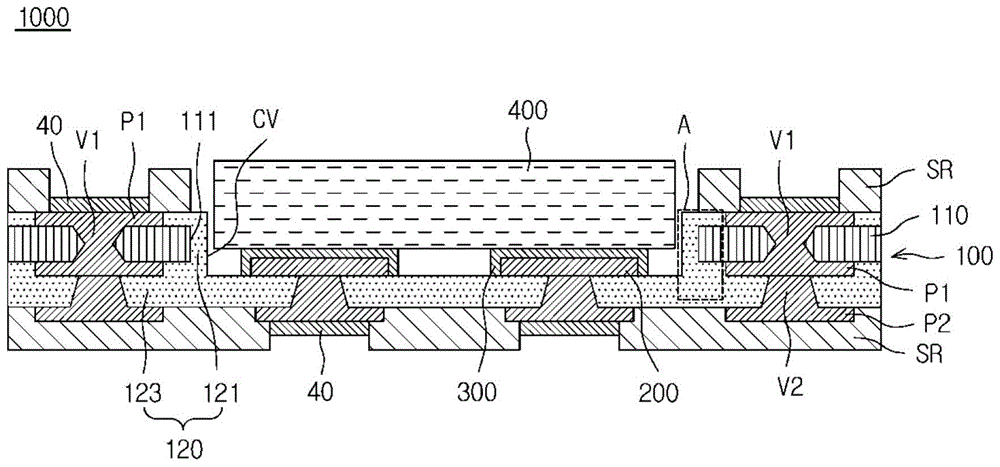
Fig. 1 is a diagram illustrating a printed circuit board according to an embodiment of the present invention. Fig. 2 is an enlarged view of a portion marked "a" in fig. 1.
Referring to fig. 1 and 2, a printed circuit board 1000 according to an embodiment of the present invention includes a laminate 100, a cavity CV, a connection terminal 200, and a resist layer 300.
Conductive patterns P1, P2 are formed in the laminate 100, and an insulating material is formed between the conductive patterns P1, P2 to insulate the conductive patterns P1, P2 from each other. That is, each of the conductive patterns P1, P2 and the insulating material are alternately stacked to form the laminate 100. Further, vias V1, V2 for penetrating the insulating material are formed in the laminate 100 to electrically connect at least a part of the conductive patterns P1, P2 to each other.
The conductive patterns P1, P2 and the vias V1, V2 may be made of conductive materials, respectively. For example, the first conductive pattern P1 may be made of copper (Cu) or any of various conductive materials such as nickel (Ni) and aluminum (Al), but is not limited thereto. The conductive patterns P1, P2 and the vias V1, V2 may be made of the same conductive material, but are not limited thereto, and it is also possible that the conductive patterns P1, P2 and the vias V1, V2 are made of different conductive materials.
The insulating material may be formed using a prepreg (PPG) having glass fibers impregnated in an insulating resin or a build-up film (build-up film) having an inorganic filler contained in an insulating resin, but is not limited thereto. In other words, any conductive material can be used to form the insulating material of the present invention.
The cavity CV formed in the laminate 100 is a space for mounting the electronic device 400 in the laminate 100. The cavity CV may be formed in various shapes and depths according to the thickness of the electronic device 400 or as required by the design.
Here, the laminate 100 may include: a first insulating layer 110 in which a receiving groove 111 is formed; and a second insulating layer 120 covering the first insulating layer 110 and including a filling part 121 and a supporting part 123, the filling part 121 being formed in the receiving groove 111 to form a cavity CV in the receiving groove 111, and the supporting part 123 being to support the filling part 121. In other words, the laminate 100 may include a first insulation layer 110 and a second insulation layer 120, the first insulation layer 110 having the receiving groove 111 formed therein, and the second insulation layer 120 including the filling part 121 and the supporting part 123 covering the first insulation layer 110. Here, the cavity CV may be formed in the receiving groove 111 by filling at least a portion of the receiving groove 111 with the filling part 121 of the second insulating layer 120.
Since the cavity CV is formed in the receiving groove 111, the receiving groove 111 has a larger diameter than the cavity CV. Here, the diameter of the receiving groove 111 may refer to the length of the longest straight line crossing the cross-section of the receiving groove 111. Similarly, the diameter of the cavity CV may be referred to the same meaning.
The first insulating layer 110 may include a first reinforcement SF1, and the first reinforcement SF1 may be exposed to an inner circumferential surface of the receiving groove 111. By forming the receiving groove 111 in the first insulating layer 110 including the first reinforcement SF1, the first reinforcement SF1 is exposed to the inner circumferential surface of the receiving groove 111. In an example, the first insulation layer 110 may be a prepreg (PPG) having glass fibers (which are the first reinforcement SF1) impregnated in an insulation resin, in which case a cross section of the glass fibers, which are the first reinforcement SF1, is exposed to the inner circumferential surface of the receiving groove 111.
The second insulation layer 120 may include the second reinforcement SF2, and a weight percentage (wt%) of the second reinforcement SF2 in the filling part 121 may be less than a weight percentage (wt%) of the second reinforcement SF2 in the supporting part 123. That is, the amount of the second reinforcement SF2 included in the filling part 121 may be less than the amount of the second reinforcement SF2 included in the supporting part 123. In an example, the second insulating layer 120 may be a prepreg having glass fibers (being the first reinforcement SF1) impregnated in an insulating resin, and the amount of glass fibers included in the filling part 121 defining the cavity CV by filling the receiving groove 111 may be smaller than the amount of glass fibers included in the supporting part 123.
The second insulating layer 120 may cover the first insulating layer 110 by using a B-stage prepreg having fluidity. That is, the second insulating layer 120 fills a space between the inner circumferential surface of the receiving groove 111 and the surface of the dummy part (dummy) (D in fig. 3) disposed in the receiving groove 111. Since the fluidity of the second reinforcement SF2 is lower than that of the insulating resin, the insulating resin forms the filling part 121. When describing a method of manufacturing a printed circuit board according to an embodiment of the present invention, the dummy part (D in fig. 3) will be described in detail.
The second insulating layer 120 may have the second conductive pattern P2 formed thereon, and the second insulating layer 120 may have the second via V2 formed therein. The second conductive pattern P2 formed on the second insulating layer 120 may be electrically connected with the first conductive pattern P1 or the connection terminal 200 formed on the first insulating layer 110 through the second via V2.
The connection terminal 200 is formed in the laminate 100 and protrudes into the cavity CV. The connection terminals electrically connect the electronic device 400 mounted in the cavity CV with the laminate 100 by protruding to the cavity CV. The shape and the pitch of the connection terminals 200 may be changed according to the shape and the pitch of the electronic devices 400 to be mounted in the cavity CV.
The connection terminal 200 may be made of a conductive material. For example, the connection terminal 200 may be made of copper (Cu) or any of various conductive materials such as nickel (Ni) and aluminum (Al), but is not limited thereto.
The resist layer 300 covers the exposed surface of the connection terminal 200 protruding to the cavity CV to prevent the connection terminal 200 from being etched. That is, when the cavity CV and the connection terminal 200 are formed in the laminate 100 by etching the dummy member D (see fig. 3), the resist layer 300 prevents the connection terminal 200 from being etched by completely covering the exposed surface of the connection terminal 200.
The resist layer 300 is made of a material that does not react with the etchant used to etch the dummy D. Specifically, in the case where the dummy piece D is made of copper (Cu), the resist layer 300 is made of a material that does not react with the copper etchant.
The resist layer 300 may be made of a material including gold (Au). Since gold (Au) has a low ionization tendency, various etchants can be selected when the dummy D is etched, and the connection terminal 200 can be prevented from being oxidized. In addition, since gold (Au) has excellent conductivity, a wide range of tolerance can be allowed when designing the external terminal and the connection terminal 200 of the electronic device 400, and signal loss can be prevented.
The resist layer 300 may include a first cover layer covering the exposed surface of the connection terminal 200 and a second cover layer covering the first cover layer. In other words, the resist layer 300 may be formed in a two-layer structure. In this case, the materials forming the first cover layer and the second cover layer may be selected by considering the combination with the materials forming the connection terminal 200 and the first cover layer.
The first capping layer may include nickel (Ni) and the second capping layer may include gold (Au). In the case where the connection terminal 200 is made of copper (Cu), the first capping layer may be made of nickel (Ni) and the second capping layer may be made of gold (Au), and in this case, the first capping layer may serve as a bonding layer that bonds the connection terminal 200 with the second capping layer.
The electronic device 400 may be an active device such as a capacitor or an inductor and/or a passive device such as an IC chip. The electronic device 400 may be mounted in the cavity CV.
Method for manufacturing printed circuit board
Fig. 3 and 9 to 16 illustrate a manufacturing process used in a method of manufacturing a printed circuit board according to an embodiment of the present invention.
Fig. 4 to 8 illustrate a manufacturing process of a dummy part used in a method of manufacturing a printed circuit board according to an embodiment of the present invention.
Referring to fig. 3, the method of manufacturing a printed circuit board according to the present embodiment includes: forming a receiving groove in the first insulating layer; dummy pieces formed so that the connection terminals and the resist layer are embedded from one surface thereof are provided in the accommodation groove.
First, a receiving groove 111 is formed in the first insulating layer 110. The first insulating layer 110 may be a prepreg (PPG) containing a first reinforcement SF1, such as, for example, glass fibers.
The receiving groove 111 may be formed by removing a portion of the first insulating layer 110 by etching or drilling (hereinafter, referred to as mechanical drilling and laser drilling). For example, the accommodation groove 111 may be formed by: a resist is formed on one surface of the first insulating layer 110, the resist opens an area of the one surface of the first insulating layer 110 corresponding to an area where the receiving groove 111 is to be formed and closes a remaining area of the one surface of the first insulating layer 110, and then the open area where the resist is not formed is etched.
The first insulating layer 110 may have a first conductive pattern P1 formed thereon. Here, the first conductive pattern P1 may be formed on the first insulating layer 110 before the receiving groove 111 is formed, or the receiving groove 111 may be formed before the first conductive pattern P1 is formed. The first conductive pattern P1 may be formed using any one of the common methods of forming circuit patterns. For example, the first conductive pattern P1 may be formed using a Copper Clad Laminate (CCL) and a subtractive process, but is not limited thereto. In another example, the first conductive pattern P1 may be formed on the first insulating layer 110 using an additive process, a semi-additive process, or a modified semi-additive process.
In the case where the first conductive patterns P1 are formed on both surfaces of the first insulating layer 110, the first via V1 may be formed in the first insulating layer 110 such that at least a portion of the first conductive patterns P1, which are respectively formed on both surfaces of the first insulating layer 110, are connected to each other. The first via V1 may be formed by processing a via hole in the first insulating layer 110 and forming a conductive material in the via hole. A via hole may be formed in the first insulating layer 110 by drilling. The first via V1 may be formed by filling a conductive paste in the via hole or plating the via hole with a conductive material. In the case where the first via V1 is formed by plating, the first via V1 and the first conductive pattern P1 may be simultaneously formed by the same plating process.
Although the first insulating layer 110 is illustrated as a single layer in fig. 3, the first insulating layer 110 may be formed as a plurality of layers according to the design or depth of the cavity CV to be formed. In this case, the first conductive pattern P1 may also be formed in multiple layers.
Next, the first insulating layer 110 in which the receiving groove 111 and the first conductive pattern P1 are formed is attached to one surface and the other surface of the detachable core (detachable core) 10. Although it is shown in fig. 3 that the first insulating layer 110 is formed on and under the removable core 10 for the purpose of efficient processing, this is merely an example, and a case where only the first insulating layer 110 is formed on or under the removable core 10 should also be covered by the scope of the present invention. Further, regardless of nomenclature, any means for temporarily supporting the first insulating layer 110 may be used as the removable core 10 of the present invention.
Then, the dummy part D is disposed in the receiving groove 111 of the first insulating layer 110. Here, the connection terminal 200 and the resist layer 300 are embedded in one surface of the dummy piece D.
Hereinafter, a manufacturing process of the dummy D according to the present embodiment will be briefly described with reference to fig. 4 to 8.
First, as shown in fig. 4, a carrier 20 having a metal foil 30 formed on one surface thereof is prepared. The carrier 20 may have a carrier metal foil 22 formed on a carrier film 21. The metal foil 30 may be made of copper (Cu) or any of various conductive materials such as nickel (Ni) and aluminum (Al), but is not limited thereto.
Then, as shown in fig. 5, the connection terminal 200 is formed on one surface of the metal foil 30. The connection terminal 200 may be formed by forming a patterned mask on the metal foil 30 using, for example, a dry film, and then filling, plating, or depositing a conductive material along the mask. In the present embodiment, the connection terminal 200 is formed by copper electroplating using the dry film as a plating resist and the metal foil 30 as a seed layer, but is not limited thereto.
Next, as shown in fig. 6, after removing the mask formed on one surface of the metal foil 30, a resist layer 300 is formed on the exposed surface of the connection terminal 200. The resist layer 300 may be formed using electroplating or electroless plating, but is not limited thereto. In the case where the dummy piece D is made of copper (Cu), the resist layer 300 may be made of a material that does not react with the copper etchant. Further, the resist 300 may be formed as a multilayer structure, in which case the multilayer structure of the resist 300 may be formed by a plurality of plating processes each using a different plating solution, and the outermost layer of the multilayer structure of the resist 300 may be made of a material that does not react with the copper etchant.
Then, as shown in fig. 7, dummy pieces D are formed on one surface of the metal foil 30 in such a manner that the resist layer 300 and the connection terminal 200 are embedded. Since the dummy part D has a shape corresponding to the shape of the receiving groove 111 and thus has a diameter smaller than that of the receiving groove 111, a plating resist having an opening corresponding to the shape and size of the dummy part D is formed on the one surface of the metal foil 30 and then plated to form the dummy part D. Dummy feature D may be formed by electroplating copper.
Then, as shown in fig. 8, the dummy piece D for use in the present embodiment is completed by separating the dummy piece D from the metal foil 30. Although the metal foil 30 is shown in fig. 8 as being first separated from the carrier 20, it may be changed according to design or as needed in the process. In the present embodiment, the metal foil 30 is separated from the carrier 20, and then the metal foil 30 is separated from the dummy pieces D.
Referring to fig. 9, the method of manufacturing a printed circuit board according to the present embodiment includes: a second insulating layer is formed on one surface of the first insulating layer and one surface of the dummy member in such a manner that the second insulating layer fills a gap between the inner surface of the receiving groove and the surface of the dummy member.
The second insulating layer 120 may be a prepreg having glass fibers (which is the second reinforcement SF2) impregnated in an insulating resin. Since the B-stage prepreg has fluidity, if the B-stage prepreg is laminated on one surface of the first insulating layer 110 and one surface of the dummy part D, the insulating resin is filled in the gap between the inner surface of the accommodation groove 111 and the surface of the dummy part D.
Meanwhile, as shown in fig. 9, in order to more easily process the B-stage second insulating layer 120, a metal single-sided laminate having the B-stage second insulating layer 120 formed on one surface thereof may be used. For example, the second insulating layer 120 may be formed on one surface of the first insulating layer 110 and one surface of the dummy D using resin-coated copper (RCC) having a B-stage insulating material formed on one surface of a copper foil.
Referring to fig. 10 and 11, the method of manufacturing a printed circuit board according to the present embodiment includes: a second via is formed in the second insulating layer and a second conductive pattern is formed on the second insulating layer. First, the via hole VH is formed in the second insulating layer 120. The via hole VH may be formed in the second insulating layer 120 by using drilling. In the case where the second insulating layer 120 is a photosensitive insulating resin, the via hole VH may be formed using photolithography. Then, the second via V2 and the second conductive pattern P2 were formed by plating.
Referring to fig. 12, the method of manufacturing a printed circuit board according to the present embodiment includes: the laminate containing the dummy is separated from the removable core. Hereinafter, for convenience of description, the lower side laminate 100 will be described separately from the removable core 10, it being understood that the same description applies to the upper side laminate 100.
Referring to fig. 13 and 14, the method of manufacturing a printed circuit board according to the present embodiment includes: a patterned solder resist SR and a surface treatment layer 40 are formed on the laminate 100.
First, as shown in fig. 13, a patterned solder resist SR formed to have an opening is formed on both surfaces of the laminate 100. The patterned solder resist SR may be formed by entirely coating both surfaces of the laminate 100 with the solder resist SR and then applying photolithography or laser drilling to the coated solder resist SR. Openings may be formed only in the first conductive pattern P1 and/or the second conductive pattern P2 as external connection pads.
Then, as shown in fig. 14, a surface treatment layer 40 is formed in the opening of the solder resist SR. In the method of manufacturing a printed circuit board according to the present embodiment, the surface treatment layer 40 may be made of a material that does not react with the etchant for etching the dummy D. That is, the surface treatment layer 40 may be made of a material including gold (Au).
Although it is described that the patterned solder resist SR is formed before the surface treatment layer 40 is formed, the surface treatment layer 40 may be formed before the patterned solder resist SR is formed.
Referring to fig. 15, the method of manufacturing a printed circuit board according to the present embodiment includes: the resist layer is exposed by etching the dummy. That is, the cavity CV is formed in the laminate 100 by removing the dummy piece D. Since the dummy part D is made of copper (Cu) in the method of manufacturing a printed circuit board according to the present embodiment, the dummy part D is removed using a copper etchant. Since the copper etchant does not react with the resist layer 300, the connection terminal 200 protected by the resist layer 300 is not removed in the cavity CV.
Referring to fig. 16, an electronic device is mounted in the cavity. The connection terminal 200 formed in the cavity CV is electrically connected to an external terminal of the electronic device 400.
Although specific embodiments of the present invention have been described above, it should be understood by those skilled in the art to which the present invention pertains that various changes and modifications of the present invention may be made without departing from the technical spirit and scope of the present invention, which should be defined by the appended claims. It is also to be understood that the claims of the present invention encompass a wide variety of other embodiments in addition to the embodiments described above.
Description of the reference numerals
CV: hollow cavity
D: dummy member
P1: first conductive pattern
P2: second conductive pattern
SF 1: first reinforcing material
SF 2: second reinforcement
SR: solder resist
V1: first path
V2: second path
VH: passage hole
10: detachable core
20: carrier
21: carrier film
22: carrier metal foil
30: metal foil
40: surface treatment layer
100: laminated part
110: a first insulating layer
111: accommodating tank
120: a second insulating layer
121: filling part
123: supporting part
200: connecting terminal
300: resist layer
400: electronic device
1000: printed circuit board
Claims (10)
Applications Claiming Priority (2)
| Application Number | Priority Date | Filing Date | Title |
|---|---|---|---|
| KR10-2015-0180330 | 2015-12-16 | ||
| KR1020150180330A KR102466204B1 (en) | 2015-12-16 | 2015-12-16 | Printed circuit board and method of manufacturing the same |
Publications (2)
| Publication Number | Publication Date |
|---|---|
| CN106888552A CN106888552A (en) | 2017-06-23 |
| CN106888552B true CN106888552B (en) | 2020-05-19 |
Family
ID=59175633
Family Applications (1)
| Application Number | Title | Priority Date | Filing Date |
|---|---|---|---|
| CN201611043463.1A Expired - Fee Related CN106888552B (en) | 2015-12-16 | 2016-11-23 | Printed circuit board and method of making the same |
Country Status (2)
| Country | Link |
|---|---|
| KR (1) | KR102466204B1 (en) |
| CN (1) | CN106888552B (en) |
Families Citing this family (4)
| Publication number | Priority date | Publication date | Assignee | Title |
|---|---|---|---|---|
| CN107613642B (en) * | 2017-08-31 | 2019-06-07 | 江苏普诺威电子股份有限公司 | The production method of the burying capacitance circuit board containing stepped groove |
| KR102501905B1 (en) * | 2017-11-09 | 2023-02-21 | 삼성전기주식회사 | Printed circuit board and method for manufacturing the same |
| WO2020246812A1 (en) * | 2019-06-04 | 2020-12-10 | 엘지이노텍 주식회사 | Printed circuit board |
| CN114449781B (en) * | 2020-10-30 | 2024-11-15 | 庆鼎精密电子(淮安)有限公司 | Method for manufacturing circuit board with embedded components |
Citations (5)
| Publication number | Priority date | Publication date | Assignee | Title |
|---|---|---|---|---|
| CN101951733A (en) * | 2009-07-08 | 2011-01-19 | 三星电机株式会社 | Insulating barrier, has the Printed circuit board and manufacturing methods of electronic component |
| CN101998772A (en) * | 2009-08-25 | 2011-03-30 | 三星电机株式会社 | Method of processing cavity of core substrate |
| CN102017821A (en) * | 2008-02-04 | 2011-04-13 | 索尼化学&信息部件株式会社 | Resist ink and method for manufacturing multilayer printed wiring board |
| CN102461350A (en) * | 2009-06-02 | 2012-05-16 | 索尼化学&信息部件株式会社 | Method for manufacturing multilayer printed wiring board |
| CN105027691A (en) * | 2012-12-26 | 2015-11-04 | Lg伊诺特有限公司 | Printed circuit board and manufacturing method thereof |
Family Cites Families (3)
| Publication number | Priority date | Publication date | Assignee | Title |
|---|---|---|---|---|
| TWI513385B (en) * | 2010-02-12 | 2015-12-11 | Lg Innotek Co Ltd | Pcb with cavity and fabricating method thereof |
| TWI610606B (en) | 2013-02-21 | 2018-01-01 | 味之素股份有限公司 | Manufacturing method and semiconductor device for built-in wiring board of parts |
| KR101601815B1 (en) * | 2014-02-06 | 2016-03-10 | 삼성전기주식회사 | Embedded board, printed circuit board and method of manufactruing the same |
-
2015
- 2015-12-16 KR KR1020150180330A patent/KR102466204B1/en active Active
-
2016
- 2016-11-23 CN CN201611043463.1A patent/CN106888552B/en not_active Expired - Fee Related
Patent Citations (5)
| Publication number | Priority date | Publication date | Assignee | Title |
|---|---|---|---|---|
| CN102017821A (en) * | 2008-02-04 | 2011-04-13 | 索尼化学&信息部件株式会社 | Resist ink and method for manufacturing multilayer printed wiring board |
| CN102461350A (en) * | 2009-06-02 | 2012-05-16 | 索尼化学&信息部件株式会社 | Method for manufacturing multilayer printed wiring board |
| CN101951733A (en) * | 2009-07-08 | 2011-01-19 | 三星电机株式会社 | Insulating barrier, has the Printed circuit board and manufacturing methods of electronic component |
| CN101998772A (en) * | 2009-08-25 | 2011-03-30 | 三星电机株式会社 | Method of processing cavity of core substrate |
| CN105027691A (en) * | 2012-12-26 | 2015-11-04 | Lg伊诺特有限公司 | Printed circuit board and manufacturing method thereof |
Also Published As
| Publication number | Publication date |
|---|---|
| KR20170072013A (en) | 2017-06-26 |
| KR102466204B1 (en) | 2022-11-11 |
| CN106888552A (en) | 2017-06-23 |
Similar Documents
| Publication | Publication Date | Title |
|---|---|---|
| US9578745B2 (en) | Printed wiring board, method for manufacturing printed wiring board and package-on-package | |
| JP6711509B2 (en) | Printed circuit board, semiconductor package and manufacturing method thereof | |
| TWI543676B (en) | Printed circuit board and method of manufacturing same | |
| US9338891B2 (en) | Printed wiring board | |
| JP2013501345A (en) | Method for manufacturing a substrate having an asymmetric build-up layer | |
| JP6795137B2 (en) | Manufacturing method of printed circuit board with built-in electronic elements | |
| KR20170037331A (en) | Printed circuit board and method for manufacturing the same | |
| KR102268388B1 (en) | Printed circuit board and manufacturing method thereof | |
| JP2015185564A (en) | Printed wiring board and printed wiring board manufacturing method | |
| JP2015220281A (en) | Printed wiring board | |
| JP5908003B2 (en) | Printed circuit board and printed circuit board manufacturing method | |
| JP2011138868A (en) | Multilayer wiring substrate | |
| CN106888552B (en) | Printed circuit board and method of making the same | |
| KR20150093032A (en) | Embedded board, printed circuit board and method of manufactruing the same | |
| JP2015170770A (en) | Printed wiring board | |
| JP5989329B2 (en) | Method for manufacturing printed circuit board | |
| KR20150065029A (en) | Printed circuit board, manufacturing method thereof and semiconductor package | |
| JP2015060981A (en) | Printed wiring board | |
| JP7497548B2 (en) | Printed Circuit Board | |
| JP5432800B2 (en) | Wiring board manufacturing method | |
| KR101580472B1 (en) | Method for manufacturing a circuit board | |
| JP2005150551A (en) | Wiring board manufacturing method | |
| JP2012160559A (en) | Method for manufacturing wiring board | |
| KR20210000161A (en) | Printed circuit board and manufacturing method the same | |
| JP6714897B2 (en) | Printed circuit board and manufacturing method thereof |
Legal Events
| Date | Code | Title | Description |
|---|---|---|---|
| PB01 | Publication | ||
| PB01 | Publication | ||
| SE01 | Entry into force of request for substantive examination | ||
| SE01 | Entry into force of request for substantive examination | ||
| GR01 | Patent grant | ||
| GR01 | Patent grant | ||
| CF01 | Termination of patent right due to non-payment of annual fee | ||
| CF01 | Termination of patent right due to non-payment of annual fee |
Granted publication date: 20200519 |