CN106027043B - Circuit device, electronic apparatus, and moving object - Google Patents
Circuit device, electronic apparatus, and moving object Download PDFInfo
- Publication number
- CN106027043B CN106027043B CN201610188201.8A CN201610188201A CN106027043B CN 106027043 B CN106027043 B CN 106027043B CN 201610188201 A CN201610188201 A CN 201610188201A CN 106027043 B CN106027043 B CN 106027043B
- Authority
- CN
- China
- Prior art keywords
- circuit
- frequency
- clock signal
- signal
- value
- Prior art date
- Legal status (The legal status is an assumption and is not a legal conclusion. Google has not performed a legal analysis and makes no representation as to the accuracy of the status listed.)
- Active
Links
- 238000001514 detection method Methods 0.000 claims abstract description 109
- 238000012545 processing Methods 0.000 claims abstract description 86
- 230000010355 oscillation Effects 0.000 claims description 149
- 238000006243 chemical reaction Methods 0.000 claims description 45
- 238000000034 method Methods 0.000 claims description 26
- 230000008569 process Effects 0.000 claims description 19
- 230000001360 synchronised effect Effects 0.000 claims description 16
- 238000005259 measurement Methods 0.000 claims description 15
- 230000006866 deterioration Effects 0.000 abstract description 9
- 230000035945 sensitivity Effects 0.000 description 28
- 235000014676 Phragmites communis Nutrition 0.000 description 26
- 230000010354 integration Effects 0.000 description 17
- 230000006870 function Effects 0.000 description 11
- 230000003321 amplification Effects 0.000 description 10
- 239000003990 capacitor Substances 0.000 description 10
- 238000003199 nucleic acid amplification method Methods 0.000 description 10
- 230000007274 generation of a signal involved in cell-cell signaling Effects 0.000 description 9
- 238000004364 calculation method Methods 0.000 description 8
- 238000012937 correction Methods 0.000 description 8
- 238000012986 modification Methods 0.000 description 8
- 230000004048 modification Effects 0.000 description 8
- 238000012546 transfer Methods 0.000 description 8
- 238000005070 sampling Methods 0.000 description 6
- 239000013078 crystal Substances 0.000 description 5
- 238000010586 diagram Methods 0.000 description 5
- 230000000630 rising effect Effects 0.000 description 5
- 238000013459 approach Methods 0.000 description 4
- 230000008859 change Effects 0.000 description 4
- 238000013461 design Methods 0.000 description 4
- 238000006073 displacement reaction Methods 0.000 description 4
- 238000007667 floating Methods 0.000 description 4
- 238000004519 manufacturing process Methods 0.000 description 4
- 238000009966 trimming Methods 0.000 description 4
- 238000005452 bending Methods 0.000 description 3
- 238000007664 blowing Methods 0.000 description 3
- 230000000052 comparative effect Effects 0.000 description 3
- 230000000694 effects Effects 0.000 description 3
- XUIMIQQOPSSXEZ-UHFFFAOYSA-N Silicon Chemical compound [Si] XUIMIQQOPSSXEZ-UHFFFAOYSA-N 0.000 description 2
- 230000001133 acceleration Effects 0.000 description 2
- 230000003139 buffering effect Effects 0.000 description 2
- 230000003111 delayed effect Effects 0.000 description 2
- 238000001914 filtration Methods 0.000 description 2
- 230000005484 gravity Effects 0.000 description 2
- 239000000463 material Substances 0.000 description 2
- 230000007246 mechanism Effects 0.000 description 2
- 230000003071 parasitic effect Effects 0.000 description 2
- 238000013139 quantization Methods 0.000 description 2
- 229910052710 silicon Inorganic materials 0.000 description 2
- 239000010703 silicon Substances 0.000 description 2
- 239000000758 substrate Substances 0.000 description 2
- 241001270131 Agaricus moelleri Species 0.000 description 1
- 101100174180 Caenorhabditis elegans fos-1 gene Proteins 0.000 description 1
- 239000008186 active pharmaceutical agent Substances 0.000 description 1
- 239000000919 ceramic Substances 0.000 description 1
- 238000013500 data storage Methods 0.000 description 1
- 230000001934 delay Effects 0.000 description 1
- 230000002542 deteriorative effect Effects 0.000 description 1
- 230000005284 excitation Effects 0.000 description 1
- 239000000284 extract Substances 0.000 description 1
- 230000036541 health Effects 0.000 description 1
- 230000003287 optical effect Effects 0.000 description 1
- 230000037081 physical activity Effects 0.000 description 1
- 238000011045 prefiltration Methods 0.000 description 1
- 239000010453 quartz Substances 0.000 description 1
- 230000009467 reduction Effects 0.000 description 1
- 239000011435 rock Substances 0.000 description 1
- 239000004065 semiconductor Substances 0.000 description 1
- 238000007493 shaping process Methods 0.000 description 1
- VYPSYNLAJGMNEJ-UHFFFAOYSA-N silicon dioxide Inorganic materials O=[Si]=O VYPSYNLAJGMNEJ-UHFFFAOYSA-N 0.000 description 1
- 239000000725 suspension Substances 0.000 description 1
- 210000000707 wrist Anatomy 0.000 description 1
Images


Classifications
-
- H—ELECTRICITY
- H03—ELECTRONIC CIRCUITRY
- H03L—AUTOMATIC CONTROL, STARTING, SYNCHRONISATION, OR STABILISATION OF GENERATORS OF ELECTRONIC OSCILLATIONS OR PULSES
- H03L7/00—Automatic control of frequency or phase; Synchronisation
- H03L7/06—Automatic control of frequency or phase; Synchronisation using a reference signal applied to a frequency- or phase-locked loop
- H03L7/16—Indirect frequency synthesis, i.e. generating a desired one of a number of predetermined frequencies using a frequency- or phase-locked loop
- H03L7/18—Indirect frequency synthesis, i.e. generating a desired one of a number of predetermined frequencies using a frequency- or phase-locked loop using a frequency divider or counter in the loop
-
- G—PHYSICS
- G01—MEASURING; TESTING
- G01C—MEASURING DISTANCES, LEVELS OR BEARINGS; SURVEYING; NAVIGATION; GYROSCOPIC INSTRUMENTS; PHOTOGRAMMETRY OR VIDEOGRAMMETRY
- G01C19/00—Gyroscopes; Turn-sensitive devices using vibrating masses; Turn-sensitive devices without moving masses; Measuring angular rate using gyroscopic effects
- G01C19/56—Turn-sensitive devices using vibrating masses, e.g. vibratory angular rate sensors based on Coriolis forces
- G01C19/5642—Turn-sensitive devices using vibrating masses, e.g. vibratory angular rate sensors based on Coriolis forces using vibrating bars or beams
- G01C19/5649—Signal processing
-
- H—ELECTRICITY
- H03—ELECTRONIC CIRCUITRY
- H03L—AUTOMATIC CONTROL, STARTING, SYNCHRONISATION, OR STABILISATION OF GENERATORS OF ELECTRONIC OSCILLATIONS OR PULSES
- H03L7/00—Automatic control of frequency or phase; Synchronisation
- H03L7/06—Automatic control of frequency or phase; Synchronisation using a reference signal applied to a frequency- or phase-locked loop
- H03L7/08—Details of the phase-locked loop
- H03L7/085—Details of the phase-locked loop concerning mainly the frequency- or phase-detection arrangement including the filtering or amplification of its output signal
-
- H—ELECTRICITY
- H03—ELECTRONIC CIRCUITRY
- H03L—AUTOMATIC CONTROL, STARTING, SYNCHRONISATION, OR STABILISATION OF GENERATORS OF ELECTRONIC OSCILLATIONS OR PULSES
- H03L7/00—Automatic control of frequency or phase; Synchronisation
- H03L7/06—Automatic control of frequency or phase; Synchronisation using a reference signal applied to a frequency- or phase-locked loop
- H03L7/08—Details of the phase-locked loop
- H03L7/099—Details of the phase-locked loop concerning mainly the controlled oscillator of the loop
-
- H—ELECTRICITY
- H03—ELECTRONIC CIRCUITRY
- H03L—AUTOMATIC CONTROL, STARTING, SYNCHRONISATION, OR STABILISATION OF GENERATORS OF ELECTRONIC OSCILLATIONS OR PULSES
- H03L7/00—Automatic control of frequency or phase; Synchronisation
- H03L7/06—Automatic control of frequency or phase; Synchronisation using a reference signal applied to a frequency- or phase-locked loop
- H03L7/16—Indirect frequency synthesis, i.e. generating a desired one of a number of predetermined frequencies using a frequency- or phase-locked loop
- H03L7/18—Indirect frequency synthesis, i.e. generating a desired one of a number of predetermined frequencies using a frequency- or phase-locked loop using a frequency divider or counter in the loop
- H03L7/181—Indirect frequency synthesis, i.e. generating a desired one of a number of predetermined frequencies using a frequency- or phase-locked loop using a frequency divider or counter in the loop a numerical count result being used for locking the loop, the counter counting during fixed time intervals
Abstract
The invention provides a circuit device, an electronic apparatus, a moving object, and the like, which can reduce deterioration of detection performance caused by an influence of a drive frequency component of a physical quantity sensor on a detection circuit. The circuit device has: a drive circuit that drives the physical quantity sensor; an FLL circuit which has a frequency comparator and an oscillator, and generates a clock signal using a signal from a driver circuit as a reference clock signal; and a detection circuit which has a circuit operating in accordance with a clock signal and which performs detection processing on a detection signal from the physical quantity sensor.
Description
Technical Field
The present invention relates to a circuit device, an electronic apparatus, a moving object, and the like.
Background
Conventionally, a circuit device for detecting a physical quantity based on a detection signal from a physical quantity sensor (transducer) is known. If a gyro sensor is taken as an example, the circuit device detects an angular velocity or the like as a physical quantity. A gyro sensor is incorporated in an electronic device such as a digital camera or a smart phone, or a mobile body such as an automobile or an airplane, and performs shake compensation, attitude control, GPS (global positioning system) automatic navigation, and the like using a physical quantity such as a detected angular velocity.
In the above-described circuit device, for example, in the case where a circuit for detecting a physical quantity, such as an a/D conversion circuit or a DSP unit (digital processing unit), is provided in the detection circuit, if a method is employed in which a clock signal generation circuit having an oscillation circuit is provided in the circuit device, and a high-speed clock signal is generated by the clock signal generation circuit, high-speed operation of these circuits can be realized.
However, when this method is employed, in the case where the physical quantity sensor is connected to the circuit device and configured as the physical quantity detection device, the driving frequency component of the driving signal for driving the physical quantity sensor may affect a circuit that operates based on the signal of the clock signal generated by the clock signal generation circuit, thereby deteriorating the detection performance.
Further, patent document 1 discloses a PLL (Phase Locked Loop) circuit in which an a/D conversion circuit performs a/D conversion on a drive signal in accordance with an output clock of a voltage controlled oscillator, and feedback-controls the voltage controlled oscillator so that the drive signal is sampled at a zero point (Phase zero of a sine wave) in the a/D conversion. Patent document 2 discloses a PLL circuit that synchronizes the phase of a digital signal with a drive signal by phase comparison using a counter. However, both patent documents 1 and 2 are techniques for generating a clock signal having a phase synchronized with a drive signal by a PLL circuit.
Patent document 1: japanese patent laid-open publication No. 2010-34722
Patent document 2: japanese patent laid-open publication No. 2012-217121
Disclosure of Invention
According to some aspects of the present invention, it is possible to provide a circuit device, an electronic apparatus, a moving object, and the like, which can reduce deterioration in detection performance due to an influence of a drive frequency component of a physical quantity sensor on a detection circuit.
One embodiment of the present invention relates to a circuit device including: a drive circuit that drives the physical quantity sensor; an FLL (Frequency Locked Loop) circuit which has a Frequency comparator and an oscillator, and generates a clock signal using a signal from the drive circuit as a reference clock signal; and a detection circuit that has a circuit that operates in accordance with the clock signal and performs detection processing on a detection signal from the physical quantity sensor.
According to one embodiment of the present invention, a clock signal is generated by an FLL circuit using a signal from a driver circuit as a reference clock signal, and a detection process is performed on a detection signal from a physical quantity sensor by a detection circuit including a circuit that operates based on the clock signal generated by the FLL circuit. This can reduce deterioration in detection performance due to the influence of the drive frequency component of the physical quantity sensor on the detection circuit.
In one aspect of the present invention, the frequency comparator may include a frequency dividing circuit that divides the frequency of the reference clock signal, and a comparator that compares a comparison target value with a reference value of the comparison target value, the comparison target value being a value obtained based on the frequency-divided clock signal from the frequency dividing circuit and the clock signal from the oscillator.
In this way, the comparison of the frequency can be performed by performing the comparison process on the comparison target value obtained based on the divided clock signal obtained by dividing the frequency of the reference clock signal and the clock signal from the oscillator and controlling the oscillation frequency of the oscillator according to the result of the frequency comparison. Further, according to this configuration, it is possible to perform frequency comparison by digital processing, and thus the frequency comparator can be simplified.
In one aspect of the present invention, the frequency comparator may include a counter that outputs a count value measured by counting a measurement period defined by the frequency-divided clock signal by the clock signal, as the comparison target value.
In this way, by counting the measurement period defined by the frequency-divided clock signal by the clock signal, the count value can be obtained as a comparison target value obtained based on the frequency-divided clock signal and the clock signal. By comparing the count value with a reference value of the count value, frequency comparison can be realized.
In one embodiment of the present invention, when the reference value is SC, the frequency division ratio of the frequency division circuit is DR, the frequency of the signal from the drive circuit is FR, and the frequency of the clock signal output from the oscillator is FV, FV may be (SC/DR) × FR.
In this way, in one embodiment of the present invention, the frequency ratio of the frequency FV of the clock signal to the frequency FR of the signal from the driver circuit is SC/DR. By fixing the frequency ratio in this manner, it is possible to reliably avoid an interference frequency at which the drive frequency component of the physical quantity sensor interferes with the operating frequency of the detection circuit, thereby reducing deterioration of detection performance.
In one embodiment of the present invention, SC/DR may be a decimal number.
Since j × FR ≠ FV/i, FV ≠ (SC/DR) × FR, SC/DR ≠ j × i. That is, by setting SC/DR to a decimal number, a clock signal in which the interference frequency is avoided can be generated.
In one embodiment of the present invention, SC may be a decimal number.
In this way, it is possible to set SC/DR to an arbitrary decimal even when the frequency division ratio DR of the frequency division circuit is small, and to set an appropriate frequency ratio SC/DR while avoiding an interference frequency.
In one aspect of the present invention, the circuit may be operated by an operation signal obtained based on the clock signal, and the SC/DR may be set so that j × FR ≠ FV/i when i is an integer of 1 or more, j is an integer of 1 or more, and the frequency of the operation signal is FV/i.
If an operating signal is generated from a clock signal from an oscillator whose frequency is not locked and the oscillation frequency of the oscillator is fos, the interference frequency is fos, which is j × FR ═ fos/i. In this regard, according to one embodiment of the present invention, SC/DR is set so that the frequency FV of the clock signal is j × FR ≠ FV/i, and since the frequency ratio SC/DR is kept constant by the FLL circuit, it is possible to reliably avoid the interference frequency.
In one aspect of the present invention, the oscillator may include a CR (resistance capacitance) oscillation circuit that is set with an oscillation frequency setting value obtained based on an output of the frequency comparator and oscillates according to the oscillation frequency setting value.
The oscillation frequency of the CR oscillation circuit varies due to temperature characteristics or manufacturing variations of a resistor, a capacitor, or a transistor constituting the CR oscillation circuit. If the clock signal generated by the CR oscillation circuit is supplied to the detection circuit, the operating frequency of the circuit may be matched with the interference frequency due to the above-described fluctuation. In this regard, according to one embodiment of the present invention, since the oscillation frequency of the CR oscillation circuit is controlled by the FLL circuit, the oscillation frequency avoiding the interference frequency can be maintained.
In one aspect of the present invention, the CR oscillation circuit may include at least one of a variable capacitance circuit and a variable resistance circuit, and the oscillation frequency of the CR oscillation circuit may be set by setting a capacitance value of the variable capacitance circuit or a resistance value of the variable resistance circuit in accordance with the oscillation frequency setting value.
In this way, by setting the capacitance value of the variable capacitance circuit or the resistance value of the variable resistance circuit in accordance with the oscillation frequency set value, it is possible to realize feedback control of the oscillation frequency by the FLL circuit, thereby maintaining the oscillation frequency avoiding the interference frequency.
In one aspect of the present invention, the CR oscillation circuit may include a variable capacitance circuit and a variable resistance circuit, and the variable resistance circuit may include: a plurality of resistance elements connected in series; and a plurality of fuse elements, each of the plurality of fuse elements being provided in parallel with each of the plurality of resistance elements, and the variable capacitance circuit being a circuit in which a capacitance value is set in accordance with the oscillation frequency setting value.
In this way, the resistance value of the variable resistance circuit can be adjusted by blowing the fuse element. Then, according to this adjustment, the oscillation frequency can be roughly adjusted so that a desired oscillation frequency is included in the adjustment range of the oscillation frequency corresponding to the oscillation frequency set value.
In one embodiment of the present invention, a loop filter may be provided between the frequency comparator and the oscillator.
In one aspect of the present invention, the loop filter may include an integrator that integrates an output of the frequency comparator, and a gain processing unit that performs gain processing on the output of the integrator.
In this way, by providing the FLL circuit with a frequency comparator and an integrator that integrates the output of the frequency comparator, feedback control of the oscillation frequency by delta sigma modulation can be performed. Thus, even when a discrete oscillation frequency is selected by the oscillation frequency setting value, a clock signal having a desired oscillation frequency on a time average can be generated.
In one embodiment of the present invention, the detection circuit may include at least one of an a/D conversion circuit and a digital signal processing unit as the circuit that operates in accordance with the clock signal.
In one embodiment of the present invention, the driving circuit may include a control unit that operates in accordance with the clock signal and controls the driving circuit and the detection circuit.
Since the driving frequency component of the physical quantity sensor interferes with the operating frequency of the a/D conversion circuit or the digital signal processing section, deterioration of detection performance may occur. In this regard, according to one aspect of the present invention, since an operating frequency that avoids an interference frequency can be realized, deterioration of detection performance can be reduced.
Another aspect of the present invention relates to an electronic device including the circuit device according to any one of the above aspects.
Another aspect of the present invention relates to a mobile body including the circuit device according to any one of the above aspects.
Drawings
Fig. 1 shows a configuration example of a circuit device according to this embodiment.
Fig. 2 shows a comparative configuration example of the circuit device.
Fig. 3 is an explanatory diagram of interference frequencies.
Fig. 4 shows a first configuration example of the FLL circuit of the present embodiment.
Fig. 5 shows a second configuration example of the FLL circuit according to the present embodiment.
Fig. 6 is an explanatory diagram of a transfer function of the FLL circuit of the present embodiment.
Fig. 7 shows a first example of setting parameters of the FLL circuit according to the present embodiment.
Fig. 8 (a) to 8 (D) are examples of operating waveforms of the FLL circuit under the setting parameters of the first example.
Fig. 9 is an example of an operation waveform of the FLL circuit under the setting parameters of the first example.
Fig. 10 shows a second example of setting parameters of the FLL circuit according to the present embodiment.
Fig. 11 (a) to 11 (C) are operation waveform examples of the FLL circuit under the setting parameters of the second example.
Fig. 12 shows a third example of setting parameters of the FLL circuit according to the present embodiment.
Fig. 13 shows an example of the configuration of an oscillator in the case where the oscillator is a CR oscillation circuit.
Fig. 14 shows a detailed configuration example of an amplifier circuit, a variable resistor circuit, and a variable capacitor circuit constituting the CR oscillation circuit.
Fig. 15 shows an example of a modified structure of the oscillator.
Fig. 16 shows an example of a modified structure of the FLL circuit.
Fig. 17 shows an example of the configuration of the arithmetic processing unit.
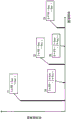
Fig. 18 shows a configuration example of a circuit device, an electronic apparatus, and a gyro sensor (physical quantity detection device) according to the present embodiment.
Fig. 19 shows a detailed configuration example of the drive circuit and the detection circuit.
Fig. 20 (a) to 20 (D) are examples of a mobile object or an electronic apparatus incorporating the circuit device of the present embodiment.
Detailed Description
Hereinafter, preferred embodiments of the present invention will be described in detail. The present embodiment described below is not intended to unduly limit the contents of the present invention recited in the claims, and all configurations described in the present embodiment are not necessarily essential as a solution of the present invention.
1. Example of Circuit device
Fig. 1 shows a configuration example of a circuit device according to the present embodiment. The circuit arrangement 20 comprises: a drive circuit 30 that drives the physical quantity sensor 12; an fll (frequency Locked loop) circuit 130 that generates a clock signal OSQ using a signal from the drive circuit 30 as a reference clock signal; the detection circuit 60 performs a detection process of the detection signal TQ from the physical quantity sensor 12.
The FLL circuit 130 is a circuit that generates a clock signal OSQ whose frequency ratio (multiple rate) with respect to the reference clock signal CKF is kept fixed (locked). The phase of the clock signal OSQ may not be synchronized with the phase of the reference clock signal CKF. The FLL circuit 130 includes a frequency comparator 132 that compares the frequencies of the reference clock signal CKF and the clock signal OSQ, and an oscillator 134 that oscillates according to a frequency corresponding to the output value QFD (output signal) of the frequency comparator 132. The frequency ratio of the reference clock signal CKF to the clock signal OSQ is locked by the feedback loop. The reference clock signal CKF is a clock signal generated from a signal in the drive circuit 30, and is, for example, a clock signal having a frequency equal to or twice the drive frequency of the physical quantity sensor 12.
The detection circuit 60 has a circuit that operates in accordance with the clock signal OSQ. That is, this circuit operates based on the clock signal OSQ whose frequency ratio is kept constant with respect to the reference clock signal CKF from the drive circuit 30.
The detection circuit 60 receives a detection signal TQ from the physical quantity sensor 12 containing a frequency component of the drive signal. That is, the circuit operating in accordance with the clock signal OSQ processes a signal containing a frequency component of the drive signal. According to the present embodiment, since the frequency ratio of the clock signal OSQ and the drive signal is kept constant by the FLL circuit 130, deterioration of detection performance due to the influence of the drive frequency component on the detection circuit can be reduced. In this regard, the following description is made in detail.
The detection circuit 60 of the present embodiment includes at least one of an a/D conversion circuit and a digital signal processing unit as a circuit that operates in accordance with the clock signal OSQ. In the following, although the case where the detection circuit 60 includes an a/D conversion circuit and a digital signal processing unit is described as an example, the present invention can be applied to the case where either one is not included.
Conventionally, these circuits are operated by signals obtained based on drive signals of the drive circuit 30 that drives the physical quantity sensor 12, but the drive frequency of the drive signals is not so high (for example, 50 to 150 kHz). Therefore, there is a problem that it is difficult to realize high-speed operation of a circuit for detecting a physical quantity, such as an a/D conversion circuit or a digital signal processing unit.
As a method for solving this problem, a method is employed in which a clock signal generation circuit having an oscillation circuit is provided in a circuit device, and a high-speed clock signal is generated by the clock signal generation circuit. Fig. 2 shows a comparative configuration example of the circuit device in this case. Fig. 2 is a comparative configuration example in the case where the physical quantity sensor is the vibrating reed 10 (angular velocity sensor element).
The circuit arrangement 20 comprises: a drive circuit 30, a detection circuit 60, and a clock signal generation circuit 70. The detection circuit 60 includes: an amplification circuit 61 that amplifies a detection signal IQ from the vibrating reed 10; a synchronous detection circuit 81 for synchronously detecting the signal from the amplifier circuit 61 by the synchronous signal SYC from the drive circuit 30; a filter unit 90 that performs low-pass filtering processing on the signal from the synchronous detection circuit 81; an a/D conversion circuit 100 that a/D converts the signal from the filter unit 90; the DSP unit 110 (digital signal processing unit) performs digital processing on the signal from the a/D conversion circuit 100 and outputs angular velocity information.
The master clock signal MCK generated by the clock signal generation circuit 70 is input to the DSP section 110, and the DSP section 110 operates in accordance with the master clock signal MCK. Further, the DSP section 110 divides the frequency of the master clock signal MCK to generate a clock signal CKAD for a/D conversion, and the a/D conversion circuit 100 performs an a/D conversion operation in accordance with the clock signal CKAD.
Since the clock signal generation circuit 70 generates the master clock signal MCK from the oscillation circuit included therein, the master clock signal MCK having a frequency higher than the driving frequency of the vibrating piece 10 can be output. This enables the a/D conversion circuit 100 or the DSP unit 110 to operate at high speed.
However, the oscillation frequency of the oscillation circuit fluctuates depending on various factors such as temperature dependency and manufacturing variation. For example, a CR oscillator is assumed as an oscillation circuit, and the oscillation frequency of the CR oscillator is not fixed according to the temperature characteristics or manufacturing variations of a capacitor or a resistor, or a transistor constituting the oscillator. When such a variation in oscillation frequency occurs, the frequency ratio between the master clock signal MCK and the drive signal also varies, and there is a possibility that a problem of a deviation of the angular velocity code due to interference between the frequency of the drive signal and the operating frequency of the a/D conversion circuit 100 or the DSP unit 110 may occur.
Fig. 3 is an explanatory diagram of interference frequencies. In fig. 3, the horizontal axis represents the oscillation frequency, and the vertical axis represents the magnitude of the angular velocity code deviation.
The oscillation frequency of the oscillation circuit included in the clock signal generation circuit 70 is fos, i, j, and k are integers equal to or greater than 1, the frequency of an operation signal such as a sampling clock signal is fsm — fos/i, and the frequency of a drive signal is FR. When i ≧ 2, i corresponds to the frequency division ratio of the clock signal, and fos/i is the frequency of the operating signal such as the sampling clock signal divided by the frequency division ratio i.
In this case, the interference frequency is an oscillation frequency when j × FR ═ k × fos/i is satisfied. That is, when the interference frequency is fin, if fos is fin, a relational expression of j × FR — k × fos/i is established.
For example, in the interference frequency shown by I1 in fig. 3, 1 × FR ═ fsm ═ fos/I holds. For example, when the interference frequency of I1 is fos 1, 1 × FR fos/I fin1/I holds. This corresponds to the case where j is 1 and k is 1 in the relational expression (interference condition) of j × FR — k × fos/i.
In the interference frequency indicated by I2, 2 × FR ═ fsm ═ fos/I holds. For example, when the interference frequency indicated by I2 is fos- fin 2, 2 × FR-fos/I-fin 2/I holds. This corresponds to the case where j is 2 and k is 1 in the relational expression of j × FR × fos/i.
In the interference frequency indicated by I3, 3 × FR ═ fsm ═ fos/I holds. For example, when the interference frequency indicated by I3 is fos-fin 3, 3 × FR-fos/I-fin 3/I holds. This corresponds to the case where j is 3 and k is 1 in the relational expression of j × FR × fos/i.
In the interference frequency indicated by I4, 3 × FR ═ 2 × fsm ═ 2 × fos/I holds. For example, when the interference frequency indicated by I4 is fos 4, 3 × FR ═ 2 × fos/I ═ 2 × fin4/I holds. This corresponds to the case where j is 3 and k is 2 in the relational expression of j × FR × fos/i.
In the interference frequency indicated by I5, 5 × FR ═ 2 × fsm ═ 2 × fos/I holds. For example, when the interference frequency indicated by I5 is fos 5, 5 × FR ═ 2 × fos/I ═ 2 × fin5/I holds. This corresponds to the case where j is 5 and k is 2 in the relational expression of j × FR × fos/i.
As described above, in the interference frequency, the interference condition represented by the relationship of j × FR ═ k × fsm ═ k × fos/i is satisfied. Here, j × FR corresponds to a harmonic component (j ≧ 2) or a fundamental component (j ═ 1) of the drive frequency FR. Fsm — fos/i is the sampling frequency (broadly, the frequency of the operating signal) of the a/D conversion circuit 100. Therefore, j × FR ═ k × fos/i as an interference condition is a condition under which the harmonic component (j ≧ 2) or the fundamental wave component (j ═ 1) of the drive frequency FR coincides with k times the sampling frequency fos/i.
The angular velocity code deviation at the interference frequency shown in fig. 3 is caused by, for example, a frequency component (driving frequency component) of an unnecessary signal mixed in the input signal of the a/D converter circuit 100 being folded back in a signal band by the sampling operation of the a/D converter circuit 100. Therefore, the angular velocity code deviation at the interference frequency is not actually expressed when j × FR and k × fsm completely coincide with each other, but is expressed remarkably when the frequency difference Δ f between j × FR and k × fsm is sufficiently small. Specifically, when the frequency difference Δ f is lower than the frequency of a signal bandwidth (for example, 200Hz to 10Hz) which is the frequency bandwidth of the desired signal, the aliasing noise generated by the frequency difference Δ f appears in the signal bandwidth, and therefore, a problem of angular velocity code deviation (rock) occurs. When the frequency difference Δ f is large, the aliasing noise is sufficiently reduced by the low-pass filter for bandwidth limitation of the DSP unit 110, and therefore, the angular velocity code deviation is not generated. In this way, it can be considered that the interference frequency to be avoided in the present embodiment has a given frequency width (signal bandwidth width, Δ f).
In the present embodiment, a method is adopted in which the frequency of the clock signal OSQ output from the FLL circuit 130 is set to a frequency at which such an interference frequency is avoided. That is, when the frequency of the clock signal OSQ is FV, i and j are integers equal to or greater than 1, and the frequency of the operating signal is FV/i, the frequency FV of the clock signal OSQ is set such that j × FR ≠ FV/i. The frequency FV/i of the operation signal is the frequency of the sampling clock signal of the a/D conversion circuit 100 or the operation clock signal (output data rate) of the DSP section 110.
Specifically, in the configuration example of the FLL circuit 130 described later with reference to fig. 4 and the like, when the reference value input to the comparator 131 is SC and the frequency division ratio of the frequency division circuit 133 is DR, FV is (SC/DR) × FR. In this case, the frequency FV of the clock signal OSQ is set to a frequency avoiding the interference frequency by setting SC/DR so that j × FR ≠ FV/i (SC/DR ≠ j × i).
In this way, if the frequency FV is set so that j × FR ≠ FV/I, the frequency FV can be set to a frequency avoiding the interference frequency (j × FR ≠ 1 × fos/I) shown in I1, I2, and I3 of fig. 3. Therefore, the occurrence of the angular velocity code deviation of a large value shown by I1, I2, I3 can be reduced, and the deterioration of the detection performance can be reduced.
In the present embodiment, it is preferable that the frequency FV is set such that j × FR ≠ k × FV/i when k is an integer equal to or greater than 1. That is, the frequency FV is set to a frequency that avoids not only the interference frequency in the case where k is 1 as shown in I1, I2, and I3 of fig. 3, but also the interference frequency (j × FR ═ k × fos/I) in the case where k is equal to or greater than 2 as shown in I4 and I5. In this way, it is possible to prevent not only the occurrence of the angular velocity code deviation of a large value shown in I1, I2, I3, but also the occurrence of the angular velocity code deviation of a relatively small value shown in I4, I5.
Further, as described above, since the oscillation frequency of the FLL circuit 130 is set to avoid the interference frequency, the phases of the reference clock signal CKF and the clock signal OSQ do not need to be locked (synchronized). That is, the frequency comparator 45 may be a circuit capable of comparing frequencies, and may not perform phase comparison. The FLL circuit 130 may be a circuit that can lock the frequency ratio between the reference clock signal CKF and the clock signal OSQ.
First configuration example of FLL Circuit
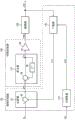
Fig. 4 shows a first configuration example of the FLL circuit according to the present embodiment. The FLL circuit 130 includes a frequency comparator 132, a loop filter 136, and an oscillator 134. The frequency comparator 132 includes a comparator 131, a frequency dividing circuit 133, and a counter 135.
The frequency dividing circuit 133 divides the frequency of the reference clock signal CKF from the drive circuit 30. The comparator 131 compares the comparison target value CTQ obtained based on the frequency-divided clock signal DVQ from the frequency dividing circuit 133 and the clock signal OSQ from the oscillator 134 with the reference value SC of the comparison target value CTQ. The counter 135 outputs a count value measured by counting the measurement period defined by the divided clock signal DVQ by the clock signal OSQ as a comparison target value CTQ.
Specifically, the cycle of the divided clock signal DVQ is a measurement period, and the counter 135 counts the clock signal OSQ during the measurement period and outputs the count value at the end of the measurement period as the comparison target value CTQ. The comparator 131 outputs an output value QFD generated based on a difference between the comparison target value CTQ and the reference value SC. The loop filter 136 provided between the frequency comparator 132 and the oscillator 134 performs filter processing (for example, integration processing, low-pass filter processing, or the like) on the output value QFD and outputs an oscillation frequency set value TRM (trimming value). The oscillator 134 is set to an oscillation frequency set value TRM obtained based on the output value QFD of the frequency comparator 132, and oscillates in accordance with the oscillation frequency set value TRM. That is, the oscillation frequency setting TRM is a setting value that can take a plurality of values within a predetermined range, and the oscillator 134 is configured such that the oscillation frequency of the oscillator 134 will change according to the setting value.
When the comparison target value CTQ does not coincide with the reference value SC, the output value QFD changes, and the oscillation frequency setting value TRM changes, the frequency of the clock signal OSQ changes, and the comparison target value CTQ changes. The oscillation frequency of the oscillator 134 is controlled by such feedback control, so that the frequency ratio of the oscillation frequency of the oscillator 134 to the frequency of the reference clock signal CKF from the drive circuit 30 is kept constant.
In the first configuration example described above, the frequency comparator 132 and the loop filter 136 may be configured by a logic circuit (digital circuit). By making it possible to configure the portion other than the oscillator 134 with a logic circuit, simplification of the circuit, reduction in area, and the like can be achieved as compared with the case of configuring with an analog circuit.
Second configuration example of FLL Circuit
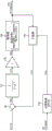
Fig. 5 shows a second configuration example of the FLL circuit according to the present embodiment. The FLL circuit 130 includes: frequency comparator 132, loop filter 136, oscillator 134. The frequency comparator 132 includes a comparator 131, a frequency dividing circuit 133, and a counter 135. The loop filter 136 includes an integrator 137 and a gain processing unit 139. In the following description, the same components as those already described are denoted by the same reference numerals, and the description thereof will be omitted as appropriate.
The comparator 131 is a differentiator, performs a difference process between the comparison target value CTQ from the counter 135 and the reference value SC, and outputs a difference value QFD obtained by the difference process.
The integrator 137 integrates the output (difference value QFD) of the frequency comparator 132, and outputs an integration value ITQ obtained by the integration. Specifically, the integrator 137 includes: a delay circuit 46 (e.g., a latch circuit or the like) that delays the integrated value ITQ by an amount corresponding to one cycle of the divided clock signal DVQ; and an adder 44 that adds the output of the delay circuit 46 and the integrated value ITQ. The output of the adder 44 becomes an integrated value ITQ.
The gain processing unit 139 performs gain processing on the output (integrated value ITQ) of the integrator 137, and outputs the gain-processed value as the oscillation frequency setting value TRM. The gain process is a process of multiplying the integrated value ITQ by a gain.
Then, the oscillator 134 oscillates at a discrete oscillation frequency according to the digital oscillation frequency setting TRM. Therefore, when the oscillation frequency setting value TRM is to be constant, the oscillation frequency is fixed to any one of discrete oscillation frequencies, and the clock signal OSQ having a desired frequency ratio with respect to the drive frequency cannot be obtained (an error occurs in the frequency ratio). In this regard, according to the present embodiment, the frequency of the clock signal OSQ can be delta-sigma (delta sigma) modulated by providing the comparator 131 (differentiator) and the integrator 137 in the loop of the FLL circuit 130. That is, the frequency of the clock signal OSQ is changed in time series by modulation, and the clock signal OSQ having a desired frequency ratio with respect to the driving frequency can be obtained as the average frequency thereof.
The detailed operation of the above configuration example will be described below. Fig. 6 is a diagram illustrating a transfer function of the FLL circuit 130 of fig. 5.
The equivalent circuit diagram of fig. 6 shows the transfer functions of the respective components. SC is the reference value and is the input of the equivalent circuit. g is the gain to be multiplied by the integral value. Q is quantization noise in the case where the oscillator 134 is regarded as a quantizer. HD2FIs a coefficient for converting the oscillation frequency setting value as a digital value into the oscillation frequency FV of the oscillator 134. In the case of, for example, a decimal digital value of 10 converted to a frequency of 200kHz, HD2F200kHz/10 kHz/20 kHz. The oscillation frequency FV is the output of the equivalent circuit. HF2DIs a coefficient for converting the oscillation frequency FV of the oscillator 134 into a count value (comparison object value) of the counter 135. In the case of, for example, converting the frequency 200kHz into a count value of 2000, HF2D2000/200kHz 10ms (100 Hz). This value corresponds to the measurement period in the counter 135. Since the counter 135 outputs the count value counted in the measurement period after the measurement period ends, the count value is a count value before 1 cycle when viewed from the loop. Therefore, a delay circuit (z) is included as an equivalent circuit of the counter 135-1)。
According to the equivalent circuit, the transfer function STF/SC of the FLL circuit 130 is expressed by formula FA. The transfer function STF is of low-pass characteristic, its DC characteristic STFDCThe transfer function STF when ω is 0) is expressed by formula FB. Further, the noise transfer function NTF/Q of the FLL circuit 130 is expressed by the formula FC. The noise transfer function NTF is known to be high-pass and less noisy at low frequencies. That is, in the case where the oscillation frequency FV is averaged over time, quantization noise is reduced.
The frequency dividing ratio of the frequency dividing circuit 133 is set to DR, and the reference clock signal from the drive circuit 30 is suppliedWhen the frequency of CKF is FR, the measurement period in the counter 135 is 1/(FR/DR) ═ DR/FR, and therefore H is setF2DDR/FR. Since DC characteristic is STF in comparison with formula FBDC=FV/SC=1/HF2DTherefore, FV/SC is FR/DR, and FV is (SC/DR) × FR. That is, the ratio of the frequency FV of the clock signal OSQ generated by the FLL circuit 130 to the frequency FR of the reference clock signal CKF from the drive circuit 30 is SC/DR.
As described in fig. 3, the interference frequency is an oscillation frequency fos at which j × FR ═ k × fos/i is satisfied. In the present embodiment, the frequency FV of the clock signal OSQ is set so that j × FR ≠ k × FV/i in order to avoid this interference frequency. That is, FV/FR is set to SC/DR ≠ (j × i)/k.
When k is 1, (j × i)/k is an integer of 1 or more, and when k is 2 or more, (j × i)/k is a fraction (decimal) or an integer of 1 or more. Therefore, in the present embodiment, SC/DR is set to a decimal number. This makes it possible to avoid at least the interference frequency when k is 1 and the interference frequency when (j × i)/k is an integer when k ≧ 2. When (j × i)/k is a fraction, the interference frequency can be avoided by setting SC/DR while avoiding the fraction.
In the present embodiment, the reference value SC may be set to a decimal number. In this case, SC/DR can be set to an arbitrary decimal even if the division ratio DR is small. That is, if the period (measurement period) for comparison by the comparator 131 is to be shortened, the frequency division ratio DR needs to be reduced. For example, when the reference value SC is an integer and the division ratio DR is 3, the decimal part excluding the integer part of SC/DR is 0.333 … or 0.666 …, and the selection of the decimal part is small. In this regard, by setting the reference value SC to a small number, SC/DR can be set to an arbitrary small number.
Note that the above-described parameters (reference value SC, frequency division ratio DR, and gain of gain processing unit 139) may be written into a register unit (e.g., register unit 142 in fig. 18) of circuit device 20 by, for example, an external processing unit (e.g., processing unit 520 in fig. 18).
Fig. 7 shows a first example of the setting parameter of the FLL circuit 130, and fig. 8 (a) to 9 show examples of the operation waveform based on the setting parameter.
As shown in fig. 7, the reference value SC is set to 16, the gain is set to 1, the frequency of the reference clock signal CKF is set to FR 50kHz, and the division ratio DR is set to 4. Let 16 gradations of the oscillation frequency setting value TRM be 0 to 15, 1 gradation of the oscillation frequency FV be 2KHz, and the oscillation frequency FV be 200KHz when TRM is 8. In this case, FV is (SC/DR) × FR is 200kHz as DC characteristics.
The change in the time series from the start of the operation is as follows. As shown in fig. 8 a, the initial value of the output (integrated value ITQ) of the integrator 137 is set to zero, for example. At this time, as shown in fig. 8 (B), since the oscillation frequency setting value TRM is 0, the oscillation frequency starts at FV 184kHz as shown in fig. 8 (D). Since the oscillation frequency FV is lower than the target 200kHz, the count value (comparison object value CTQ) is smaller than the reference value SC of 16, and becomes a difference value QFD > 0. Therefore, the integrated value ITQ increases, the oscillation frequency setting value TRM increases, and the oscillation frequency FV rises. This operation is repeated, and the target FV is 200 kHz.
Fig. 9 is a timing chart corresponding to the time-series change described above. As shown in fig. 9, the counter 135 outputs a count value at the rising edge of the divided clock signal DVQ. That is, the counter 135 is reset at the rising edge of the frequency-divided clock signal DVQ, and the clock signal OSQ is counted with the period from the time of the reset to the next time of the reset as the measurement period, and the count value is output as the comparison target value CTQ.
The differentiator 42, the integrator 137, and the gain processing section 139 operate in synchronization with the rise of the frequency-divided clock signal DVQ. That is, the differentiator 42 outputs a difference value QFD of the reference value SC and the comparison object value CTQ at the rising edge of the divided clock signal DVQ. In the integrator 137, a circuit (z) is delayed at the rising edge of the divided clock signal DVQ-1) Operates to further the integration value ITQAnd (5) new. The gain processing section 139 outputs the oscillation frequency setting value TRM at each rising edge of the frequency-divided clock signal DVQ.
The numerical values described in the timing chart of the comparison object value CTQ (count value), the integrated value ITQ, and the oscillation frequency setting value TRM correspond to the waveforms in fig. 8 (C), fig. 8 (a), and fig. 8 (B). It is understood that the oscillation frequency setting value TRM gradually approaches the TRM corresponding to the target 200kHz, which is equal to 8, from the TRM which is the initial value being equal to 0.
A second example of the setting parameter of the FLL circuit 130 is shown in fig. 10, and (a) in fig. 11 to (C) in fig. 11 indicate operation waveform examples based on the setting parameter. The second example is an example of a case where the same frequency as the target is not included in the gradation of the oscillation frequency FV.
As shown in fig. 10, the reference value SC is 320, the gain 1/32, the frequency FR of the reference clock signal CKF is 50kHz, and the division ratio DR is 32. Let 16 gray scales of the oscillation frequency setting value TRM be 0 to 15, 1 gray scale of the oscillation frequency FV be 1kHz, and the oscillation frequency FV be 498.2kHz when TRM is 8. In this case, FV is (SC/DR) × FR is 500kHz as the DC characteristic.
As shown in fig. 11 (a) to 11 (C), the case where the oscillation frequency FV gradually approaches the target 500kHz in the time series from the start of the operation is the same as the first example described above. In the second example, after approaching the target 500kHz, the oscillation frequency FV is not fixed but varied by delta sigma modulation. That is, since FV is 499.2KHz when TRM is 9 and FV is 500.2KHz when TRM is 10, TRM is alternately set to 9 or 10 so as to be 500KHz on average by delta sigma (delta sigma) modulation.
Fig. 12 shows a third example of setting parameters of the FLL circuit 130. The third example is an example in the case where SC/DR is set to a decimal number.
As shown in fig. 12, the reference value SC is 40.4, the gain is 1/40.4, the frequency of the reference clock signal CKF is FR 50kHz, and the frequency division ratio DR is 4. Let the model of the oscillator 134 be the same as that of fig. 10. The frequency setting value TRM is set to 16 gradations of 0 to 15, 1 gradation of the oscillation frequency FV is 1kHz, and the oscillation frequency FV is 503.2kHz when TRM is 8. In this case, FV is (SC/DR) × FR 505KHz as DC characteristics.
4. Oscillator
Hereinafter, the oscillator 134 will be described in detail by taking a case where the oscillator 134 is a CR oscillation circuit as an example.
The CR oscillation circuit of the present embodiment includes at least one of a variable capacitance circuit and a variable resistance circuit. Then, the oscillation frequency FV of the CR oscillation circuit is set by setting the capacitance value of the variable capacitance circuit or the resistance value of the variable resistance circuit based on the oscillation frequency setting value TRM.
Fig. 13 shows a detailed configuration example of the oscillator 134 in this case. The CR oscillation circuit as the oscillator 134 includes: a capacitor C, a variable resistance circuit 196 (first frequency adjustment unit), a variable capacitance circuit 197 (second frequency adjustment unit), and an amplification circuit 180 (buffer circuit).
The CR oscillation circuit is supplied with a power supply voltage VDOS to operate, and generates a clock signal OSQ (oscillation signal). Specifically, the CR oscillation circuit generates an oscillation signal by feeding back a signal to an input terminal using an RC circuit composed of a capacitor and a resistor. Then, a signal obtained by waveform shaping the generated oscillation signal is output as the clock signal OSQ.
The amplifier circuit 180 (inverting amplifier circuit) has inverter circuits IV0, IV1, and IV 2. The output of the inverter circuit IV1 is fed back to the input node NI of the amplifier circuit 180 via the capacitor C. The output of the inverter circuit IV2 is fed back to the input node NI of the amplifier circuit 180 via the variable resistor circuit 196 (R). The input of the inverter circuit IV0 becomes the input of the amplifier circuit 180.
The oscillation signal output from the inverter circuit IV2 is waveform-shaped by the inverter circuit IV3 and is output as a clock signal OSQ of a rectangular wave. In addition, it is also possible to provide a frequency dividing circuit at a subsequent stage of the inverter circuit IV3 and output one or more clock signals obtained by dividing the clock signal OSQ.
In this configuration example, in a state where the physical quantity sensor 12 and the circuit device 20 are connected and the FLL circuit 130 is operating, the capacitance value of the variable capacitance circuit 197 is set in accordance with the oscillation frequency set value TRM. Thereby, the oscillation frequency of the CR oscillation circuit is controlled by the loop of the FLL circuit 130. The variable capacitance circuit 197 is a circuit whose capacitance value can be variably adjusted, and the capacitance value of the RC circuit is changed by changing the capacitance value of the variable capacitance circuit 197, thereby setting the oscillation frequency of the CR oscillation circuit.
On the other hand, before the physical quantity sensor 12 and the circuit device 20 are connected, the oscillation frequency of the CR oscillation circuit is adjusted by the variable resistance circuit 196. At this time, the oscillation frequency of the CR oscillation circuit is adjusted to the vicinity of the oscillation frequency of the target (frequency at which the interference frequency is avoided). That is, the resistance value of the variable resistance circuit 196 is adjusted so that the target oscillation frequency (frequency at which the disturbance frequency is avoided) falls within the range of the oscillation frequency that can be set by the oscillation frequency setting value TRM. The variable resistor circuit 196 is a circuit whose resistance value can be variably adjusted, and the resistance value of the RC circuit is changed by changing the resistance value of the variable resistor circuit 196, thereby setting the oscillation frequency of the CR oscillation circuit.
In this way, in the present embodiment, it is possible to realize the adjustment (rough adjustment) of the oscillation frequency in the state before the physical quantity sensor 12 and the circuit device 20 are connected, and the locking (control of keeping the ratio of the drive frequency and the oscillation frequency constant) of the oscillation frequency by the FLL circuit 130 in the state where the physical quantity sensor 12 and the circuit device 20 are connected. With this, it is possible to generate the clock signal OSQ at a frequency avoiding the interference frequency, and it is possible to reduce deterioration of the detection performance due to the above-described interference.
In fig. 13, the case where the CR oscillation circuit includes the variable capacitance circuit 197 and the variable resistance circuit 196 and the capacitance value of the variable capacitance circuit 197 is set in accordance with the oscillation frequency setting value TRM has been described as an example, but the configuration of the CR oscillation circuit is not limited to this. For example, one of the variable capacitance circuit 197 and the variable resistance circuit 196 may not be included. Alternatively, the oscillation frequency may be controlled by setting the resistance value of the variable resistance circuit 196 according to the oscillation frequency set value TRM. Alternatively, the oscillation frequency may be controlled by including a voltage generation circuit, not shown, and changing the power supply voltage VDOS in accordance with the oscillation frequency set value TRM. Alternatively, a voltage generation circuit not shown may be included, and the oscillation frequency may be roughly adjusted by roughly adjusting power supply voltage VDOS generated by the voltage generation circuit.
Fig. 14 shows a detailed configuration example of the amplifier circuit 180, the variable resistor circuit 196, and the variable capacitor circuit 197 that constitute the CR oscillation circuit.
The amplifier circuit 180 includes a NAND circuit NA and inverter circuits IV1 and IV 2. The output of the inverter circuit IV1 is fed back to the input node NI of the amplifier circuit 180 via the capacitor C. The output of the inverter circuit IV2 is fed back to the input node NI of the amplifier circuit 180 via the variable resistor circuit 196. A first input terminal of the NAND circuit NA serves as an input terminal of the amplifier circuit 180, and the enable signal EN is input to a second input terminal of the NAND circuit NA. The CR oscillation circuit is set to an operation enable state when the enable signal EN becomes H level, and is set to an operation disable state when the enable signal EN becomes L level.
The variable resistor circuit 196 includes: a plurality of resistance elements R1 to R6 connected in series; the plurality of fuse elements FU1 to FU6 (broadly, switching elements) are connected in parallel, and the fuse elements FU1 to FU6 are connected in parallel to the resistor elements R1 to R6. For example, the fuse element FU1 is connected in parallel to the resistor element R1, and the fuse element FU2 is connected in parallel to the resistor element R2. The connection structures of the fuse elements FU3 to FU6 and the resistor elements R3 to R6 are also the same. The variable resistor circuit 196 includes a reference resistor element R7 connected in series to the plurality of resistor elements R1 to R6. That is, the plurality of resistance elements R1 to R6 and the reference resistance element R7 are connected in series between the output node NQ and the input node NI of the amplifier circuit 180.
The variable capacitance circuit 197 includes variable capacitance elements CV1 to CV4 and capacitance control voltage output circuits BC1 to BC 4. One ends of the variable capacitance elements CV1 to CV4 are connected to an output node NQ of the amplifier circuit 180, and the other ends are connected to output ends of capacitance control voltage output circuits BC1 to BC 4. The variable capacitance elements CV1 to CV4 are elements whose capacitances change in accordance with the capacitance control voltages output from the capacitance control voltage output circuits BC1 to BC 4. The capacitance control voltage is set to a voltage corresponding to the oscillation frequency set value TRM. The variable capacitance elements CV1 to CV4 can be realized by, for example, variable capacitance (variable capacitance). The variable capacitance circuit 197 can be realized by an array of variable capacitance elements weighted in a binary manner, for example, and in this case, the control based on the capacitance control voltage is binary control of high level and low level. For example, when the oscillation frequency setting value TRM is 4 bits, the capacitance control voltage output circuits BC1 to BC4 output the logic levels of the first to fourth bits from the LSB side thereof, respectively.
5. Adjustment of oscillation frequency using variable resistance circuit
Next, a method of adjusting the oscillation frequency using the variable resistor circuit 196 will be described. The oscillation frequency is adjusted to a desired oscillation frequency by using the variable resistance circuit 196 for element variations such as transistors and resistors implemented by the semiconductor wafer processor.
The resistance values of the resistance elements R1 to R6 of the variable resistance circuit 196 in fig. 14 are weighted in a binary manner, for example. Each of the resistance elements R1 to R6 is composed of one or a plurality of resistance units. For example R1 from 20R2 is composed of 2 connected in series, 1 resistance element 12 resistance units, R3 being 2 serially connected2And each resistance unit. Similarly, R4, R5 and R6 are each composed of 2 s connected in series 32, 242, 25And each resistance unit. Therefore, when the resistance value of the unit resistance is RU, the resistance value of R1 is set to 20Xru (═ RU), the resistance value of R2 was setIs defined as 21Xru (═ 2 × RU), the resistance value of R3 was set to 22XRU, the resistance value of R4 was set to 23XRU, the resistance value of R5 was set to 24XRU, resistance value of R6 is 25×RU。
On the other hand, R7 is a reference resistance element for setting an oscillation frequency to be a reference, and when RB is a reference resistance value that is a resistance value of R7, RB can be set to a resistance value that is approximately the same as R6, for example. By setting in this way, it is possible to set the range within a predetermined range (for example, RB to RB + RU × (2)6Range of-1)) variably sets the resistance value of the variable resistance circuit 196.
As shown in fig. 14, fuse elements FU1 to FU6 and resistor elements R1 to R6 are provided in parallel. Before the fuse is blown, all fuse elements FU1 to FU6 are in the non-blown state. Therefore, the resistance value of the variable resistance circuit 196 is set to the reference resistance value RB of R7 (precisely, RB + parasitic resistance value of the fuse element and the like). In this state, the oscillation frequency of the CR oscillation circuit is measured. When the measured oscillation frequency is fr, the fuse value is calculated by a trimming equation (trimming equation) expressed by a linear equation of fr as shown in the following equation (1). And a and b are constants.
Fuse value as a x fr + b (1)
Which of the fuse elements FU 1-FU 6 is blown (trimmed) is determined based on the calculated fuse value. For example, fuse elements FU1, FU3, FU4 and FU5 are blown based on the fuse value calculated by the trimming equation. In this case, the resistance value of the variable resistance circuit 196 becomes RB + R1+ R3 + R4+ R5(+ parasitic resistance value).
Specifically, the blown fuse element can be determined by converting the fuse value (the fuse value after conversion to an integer) into data expressed in binary. For example, if the fuse value is 1 or 20Blowing fuse element FU1, if fuse value is 2 or 21Fuse element FU2 is blown. In addition, if the fuse value is 3 or 20+21Then, thenFusing FU1 and FU2 if fuse value is 4-22Blowing fuse element FU3, if fuse value is 5 or 20+22Fuse elements FU1 and FU3 are blown. That is, fuse element FU1 corresponds to LSB, fuse element FU2 corresponds to the next bit of LSB, and fuse element FU3 corresponds to the next bit of LSB. Likewise, fuse element FU6 corresponds to the MSB of the fuse value in binary representation. Fuse element FU1 is blown if the LSB of the fuse value is 1, and is not blown if it is zero. If the next bit of the LSB is a 1, fuse element FU2 is blown and if zero, it is not blown.
6. Modifications of oscillators
Although the case where the oscillator 134 is a CR oscillation circuit has been described above as an example, the oscillator 134 is not limited to this configuration. For example, the oscillator 134 may have the structure shown in fig. 15.
The oscillator 134 shown in fig. 15 includes: a D/a conversion circuit 72 that performs D/a conversion on the oscillation frequency set value TRM; and a voltage controlled oscillator 74 that oscillates in accordance with the analog output voltage DAQ from the D/a conversion circuit 72. When the oscillator 134 is applied to the FLL circuit 130 according to the present embodiment, the output voltage DAQ of the D/a conversion circuit 72 changes in accordance with the oscillation frequency set value TRM, and the frequency of the clock signal OSQ changes accordingly, and the frequency is fed back to the oscillation frequency set value TRM via the frequency comparator 132 and the loop filter 136. Although the analog output voltage DAQ has a discrete voltage value, as described with reference to fig. 5 and the like, the clock signal OSQ having a desired frequency is output as an average value by delta sigma (delta sigma) modulation.
Modification of FLL Circuit
Although the case where the frequency comparator 132 and the loop filter 136 of the FLL circuit 130 are configured by logic circuits has been described above as an example, the FLL circuit 130 is not limited to this configuration. For example, as shown in fig. 16, the frequency comparator 132 or the loop filter 136 may be formed of an analog circuit.
The FLL circuit 130 shown in fig. 16 includes: a frequency comparator 45, a loop filter 43, an oscillator 48, and a frequency dividing circuit 41.
The frequency dividing circuit 41 divides the clock signal OSQ and outputs a frequency-divided clock signal DVOS. The frequency comparator 45 compares the frequency of the reference clock signal CKF with the frequency of the frequency-divided clock signal DVOS, and outputs an analog signal QP derived based on the difference therebetween. For example, the frequency comparator 45 is implemented by a charge pump circuit. The loop filter 43 performs low-pass filtering processing on the analog signal QP, and outputs a voltage obtained by the processing as the control voltage VLQ. For example, the loop filter 136 is implemented by a passive low-pass filter composed of a capacitor or a resistor. The oscillator 48 oscillates at a frequency corresponding to the control voltage VLQ and outputs a clock signal OSQ. For example, oscillator 48 is implemented by a Voltage Controlled Oscillator (VCO).
8. Arithmetic processing unit
According to the FLL circuit 130 described above, the a/D conversion circuit 100 or the DSP unit 110 can be operated by the clock signal OSQ (or the operation clock signal obtained by dividing the reference clock signal CKF from the driver circuit 30 by SC/DR).
At this time, since the driving frequency of the physical quantity sensor 12 varies due to manufacturing variations and the like, the frequency of the clock signal OSQ also varies in accordance with the variation of the frequency. For example, in a gyro sensor, angular velocity information is obtained by integrating angular velocity information, but the operating frequency of the DSP unit 110 or the like changes, and the integration period changes, which may cause an error in the angular velocity information.
Therefore, in the present embodiment, the following processing is performed by the arithmetic processing unit 150 provided at the subsequent stage of the detection circuit 60, whereby more accurate angular velocity information can be obtained. The arithmetic processing unit 150 may be included in the DSP unit 110 of the detection circuit 60.
Fig. 17 shows a configuration example of the arithmetic processing unit 150. The arithmetic processing unit 150 includes a multiplication processing unit 155 and an integration processing unit 156, and operates using an operation clock signal obtained by dividing the clock signal OSQ by DO (that is, using the reference clock frequency FR and operating using an operation clock signal having a frequency represented by (SC/DR) × FR/DO). The multiplication unit 155 performs multiplication based on the angular velocity information QG (physical quantity information) from the detection circuit 60 and an arithmetic coefficient CF (driving frequency information in a broad sense) whose value is set in accordance with the driving frequency of the driving circuit 30. The integration processor 156 receives the multiplication result QM (for example, angular displacement) of the multiplier 155, and performs integration processing on the multiplication result QM. Thereby, the integration processing of the angular velocity information QG is realized. The integration processing unit 156 outputs the rotational speed information QH. The rotation speed information QH includes an integer part REVQ and a decimal part DEGQ represented by a fixed decimal point.
The arithmetic coefficient CF is a coefficient whose value is set in accordance with the driving frequency of the driving circuit 30 as described later. More specifically, the value of the coefficient is set according to the set sensitivity of the drive frequency and the angular velocity information. The multiplication unit 155 performs a process of multiplying the angular velocity information QG by the operation coefficient CF, thereby realizing an operation process based on time interval information defined by the driving frequency of the driving circuit 30.
More specifically, the multiplication unit 155 includes a multiplier MLA. The multiplication unit 155 performs multiplication processing of multiplying the angular velocity information QG (gyro signal) by an arithmetic coefficient CF (fixed number). Thereby, the angular displacement (Δ θ) within the time interval of the data rate is calculated. The angular displacement is obtained by multiplying the angular velocity by the time interval. The time interval is set by the arithmetic coefficient CF.
The arithmetic coefficient CF input to the multiplication unit 155 is expressed by, for example, the following expression (2).
CF=1/(360×SEN×fxt×(SC/DR)/DO) (2)
In the above equation (2), SEN represents the set sensitivity (LSB/dps), and fxt represents the drive frequency (Hz) of the vibrating reed 10 (crystal vibrating reed). Specifically, the set sensitivity SEN is a sensitivity of an angular velocity set as a specification (design value) of the physical quantity detection device (gyro sensor). That is, the set sensitivity SEN is uniquely determined as a product specification so that SEN is 300(LSB/dps), for example. Further, a drive signal of the vibrating reed 10 (or a signal obtained based on the drive signal) is used as the reference clock signal, and fxt is a drive frequency measured in a state where the circuit device 20 is connected to the vibrating reed 10. That is, fxt is a drive frequency set based on the measurement result of the drive frequency. The arithmetic coefficient CF is not limited to the above expression (2), and various changes such as a coefficient obtained by multiplying the above expression (2) by a predetermined constant can be performed.
In this way, in the present embodiment, the arithmetic processing (multiplication) by the arithmetic processing unit 150 is performed using the arithmetic coefficient CF whose value is set in accordance with the drive frequency (fxt) of the drive circuit 30 and the set Sensitivity (SEN) of the angular velocity (physical quantity information). The drive frequency (fxt) used for setting the arithmetic coefficient CF is a numerical value set based on the measurement result of the drive frequency. Specifically, in the present embodiment, the operation coefficient CF of the above expression (2) is written in the nonvolatile memory 146 as drive frequency information (information whose value is set according to the drive frequency). The arithmetic processing unit 150 reads the arithmetic coefficient CF as the drive frequency information from the nonvolatile memory 146, and performs arithmetic processing based on time interval information defined by the drive frequency information.
The driving frequency of the driving circuit 30 is deviated from a design value. For example, the deviation occurs from the design value (50kHz to 200kHz) of the drive frequency. In the present embodiment, since the time interval information in the calculation process of the calculation processing unit 150 is defined by the drive frequency, if there is a variation in the drive frequency, a variation also occurs in the calculation result. For example, when the detection target is actually rotated by 10 degrees, if there is a deviation in the drive frequency, the rotation angle as the calculation result of the calculation processing unit 150 does not become 10 degrees, but becomes an angle not matching 10 degrees.
In this regard, in the present embodiment, the drive frequency is measured in a state where the vibrating reed 10 is connected to the circuit device, and as shown in the above expression (2), the arithmetic coefficient CF (broadly, drive frequency information) is obtained from the measured drive frequency (fxt) and stored in the nonvolatile memory 146. The arithmetic processing unit 150 performs arithmetic processing based on the arithmetic coefficient CF read from the nonvolatile memory 146. Therefore, since the time interval information used in the calculation process is defined based on the measured drive frequency (fxt), the calculation processing unit 150 can output a more accurate calculation result even when there is a variation in the drive frequency.
The angular velocity detected by the detection circuit 60 is subjected to sensitivity correction by the DSP unit 110, and is corrected so that the sensitivity of the angular velocity becomes a set sensitivity that is a design value. The value of the set sensitivity may vary depending on the product of the physical quantity detection device, and when the arithmetic processing unit 150 performs arithmetic processing such as integration processing without considering the set sensitivity, an accurate arithmetic result cannot be obtained.
In this regard, in the present embodiment, as shown in the above expression (2), the arithmetic coefficient CF is obtained from the set sensitivity SEN, and the arithmetic processing unit 150 performs arithmetic processing based on the arithmetic coefficient CF. Therefore, the arithmetic processing can be performed based on the arithmetic coefficient CF corresponding to the sensitivity of the angular velocity output from the detection circuit 60. For example, when the set sensitivity SEN is 300(LSB/dps), the sensitivity of the angular velocity output from the detection circuit 60 is also set to 300(LSB/dps), and the angular velocity from the detection circuit 60 is multiplied by the arithmetic coefficient CF that sets the set sensitivity SEN to the denominator in the manner of expression (2) above, whereby an accurate arithmetic result that does not depend on the sensitivity can be obtained.
The integration processing unit 156 includes a floating-point integrator 160 (floating-point integrator) and a fixed-point integrator 164 (fixed-point integrator). The detector 162, the fixed point conversion unit 166, and the registers 168 and 169 may be provided.
The floating-point integrator 160 integrates the angular displacement in the floating-point form (Δ θ ═ ω × t), thereby calculating the angle. Here, in order to perform integration without reducing the precision of the floating-point operation, it is preferable that the value of the output of the floating-point integrator 160 is always set to a small value (for example, 2)-16Below). Therefore, when the value of the output of the floating-point integrator 160 crosses a fixed value, a process of subtracting this amount is performed. For example, when the detector 162 determines that the value of the output of the floating-point integrator 160 exceeds, for example, 2-16In this case, a process of subtracting a subtraction amount of "+ 1" from the integration result (output value), for example, is performed, and a process of adding an addition amount "+ 1" corresponding to the subtraction amount to the other fixed point integrator 164 is performed. The conversion to fixed point is also performed at this time. Similarly, when it is determined that the value of the output of the floating-point integrator 160 exceeds, for example, 2-15In this case, a process of subtracting a subtraction amount of "+ 2" from the integration result, for example, and a process of adding the addition amount "+ 2" corresponding to the subtraction amount to the fixed point integrator 164 are performed. In excess of 2-14、2-13、2-12、2-11The subtraction amount and the addition amount in the case of (1) are "+ 4", "+ 8", "+ 16", and "+ 32", respectively.
The output of the fixed point integrator 164 and the like are output as an integer part REVQ and a decimal part DEGQ of the rotational speed information via the register 168 and the register 169.
In fig. 17, the output of the floating-point integrator 160 represented by a floating point is directly converted with respect to the minute angle component (lower 8 bits) without passing through the fixed-point integrator 164. For example, the value shown in the exponent part of a floating point number is 2-15In the case of (1), the 8 th bit is set to 1, and the upper 7 bits of the mantissa portion of the floating-point number are output as the lower 7 bits, whereby conversion to the fixed-point number is performed. This conversion is performed by the fixed point conversion section 166, and the obtained 8-bit fixed point number is output to the register 169. Similarly, the exponent part of a floating-point number indicates a value of 2-14In the case of (1), the 8 th and 7 th bits are set to 0 and 1, and the upper 6 th bit of the mantissa part of the floating point number is set to the lower bitAnd 6 bits are output to perform conversion to fixed point numbers.
As described above, in fig. 17, the arithmetic processing unit 150 performs arithmetic processing on the angular velocity information QG (physical quantity information) represented by a floating point number, and outputs the rotational speed information QH (post-arithmetic physical quantity information) represented by a fixed point number. The rotation speed information QH (angle information) represented by the fixed point number is composed of an integer part REVQ and a decimal part DEGQ.
9. Detailed structure of electronic device, gyro sensor, and circuit device
Fig. 18 shows a detailed configuration example of the circuit device 20 of the present embodiment, the gyro sensor 510 (broadly, the physical quantity detection device) including the circuit device 20, and the electronic apparatus 500 including the gyro sensor 510.
The circuit device 20, the electronic apparatus 500, and the gyro sensor 510 are not limited to the configuration shown in fig. 18, and various modifications may be made such as omitting a part of the components and adding another component. As the electronic device 500 of the present embodiment, various devices such as a digital camera, a video camera, a smart phone, a mobile phone, a car navigation system, a robot, a biological information detection device, a game machine, a clock, a health appliance, or a portable information terminal can be assumed. In the following, a case will be described in which the physical quantity sensor (angular velocity sensor element) is a piezoelectric vibrating reed (vibration gyro) and the sensor is a gyro sensor, but the present invention is not limited to this. For example, the present invention can also be applied to a capacitance detection type vibration gyro formed of a silicon substrate or the like, a physical quantity sensor that detects a physical quantity equivalent to angular velocity information or a physical quantity other than angular velocity information, and the like.
The electronic device 500 includes a gyro sensor 510 and a processing unit 520. The memory 530, the operation unit 540, and the display unit 550 may be included. A processing unit 520 (external processing device) implemented by a CPU, MPU, or the like performs control of the gyro sensor 510 or the like or overall control of the electronic apparatus 500. The processing unit 520 performs processing based on the angular velocity information (broadly, physical quantity) detected by the gyro sensor 510. For example, processing for shake correction, attitude control, GPS automatic navigation, and the like is performed based on the angular velocity information. The memory 530(ROM, RAM, etc.) stores a control program and various data, and functions as a work area or a data storage area. The operation unit 540 is a member for a user to operate, and the display unit 550 displays various kinds of information to the user.
The gyro sensor 510 (physical quantity detecting device) includes the vibrating piece 10 and the circuit device 20. The vibrating reed 10 (broadly, a physical quantity sensor and an angular velocity sensor) is a piezoelectric vibrating reed formed of a thin plate of a piezoelectric material such as crystal. Specifically, the vibrating reed 10 is a double-T-shaped vibrating reed formed by a Z-cut crystal substrate.
The circuit arrangement 20 comprises: the drive circuit 30, the FLL circuit 130, the detection circuit 60, the control unit 140, the register unit 142, the output unit 144 (interface unit), the nonvolatile memory 146, and the arithmetic processing unit 150. Various modifications may be made to omit some of these components or to add other components.
The FLL circuit 130 generates a clock signal in accordance with a signal from the drive circuit 30. The detection circuit 60 includes an a/D conversion circuit 100 and a DSP unit 110, and the a/D conversion circuit 100, the DSP unit 110, an arithmetic processing unit 150, and a control unit 140 operate based on a clock signal from the FLL circuit 130 or a clock signal obtained by dividing the clock signal.
The control unit 140 performs control processing of the circuit device 20. The control unit 140 can be realized by a logic circuit (gate array or the like), a processor, or the like. Various kinds of switching control, mode setting, and the like of the circuit device 20 are performed by the control unit 140.
The drive circuit 30 outputs a drive signal DQ and drives the vibrating element 10. For example, the vibration element 10 is excited by receiving the feedback signal DI from the vibration element 10 and outputting the drive signal DQ corresponding thereto. The detection circuit 60 receives detection signals IQ1 and IQ2 (detection current and charge) from the vibrating element 10 driven by the drive signal DQ, and detects (extracts) a desired signal (coriolis force signal) corresponding to a physical quantity applied to the vibrating element 10 based on the detection signals IQ1 and IQ 2.
The vibrating reed 10 includes: the base 1, the connecting arms 2, 3, the driving arms 4, 5, 6, 7, and the detecting arms 8, 9. The detection arms 8 and 9 extend in the + Y-axis direction and the-Y-axis direction with respect to the rectangular base 1. The connecting arms 2 and 3 extend in the-X axis direction and the + X axis direction with respect to the base 1. The drive arms 4 and 5 extend in the + Y axis direction and the-Y axis direction with respect to the connecting arm 2, and the drive arms 6 and 7 extend in the + Y axis direction and the-Y axis direction with respect to the connecting arm 3. The X, Y, and Z axes are axes representing crystal axes and are referred to as electrical, mechanical, and optical axes, respectively.
The drive signal DQ from the drive circuit 30 is input to drive electrodes provided on the upper surfaces of the drive arms 4, 5 and drive electrodes provided on the side surfaces of the drive arms 6, 7. Signals from the drive electrodes provided on the side surfaces of the drive arms 4 and 5 and the drive electrodes provided on the upper surfaces of the drive arms 6 and 7 are input to the drive circuit 30 as a feedback signal DI. Further, signals from the detection electrodes provided on the upper surfaces of the detection arms 8 and 9 are input to the detection circuit 60 as detection signals IQ1 and IQ 2. The common electrode provided on the side surfaces of the detection arms 8 and 9 is grounded, for example.
When the ac drive signal DQ is applied by the drive circuit 30, the drive arms 4, 5, 6, and 7 perform bending vibration (excitation vibration) as indicated by arrow a by the inverse piezoelectric effect. That is, bending vibration is performed in which the distal ends of the drive arms 4 and 6 repeatedly approach and separate from each other, and the distal ends of the drive arms 5 and 7 also repeatedly approach and separate from each other. At this time, since the driving arms 4 and 5 and the driving arms 6 and 7 perform line-symmetric vibration with respect to the Y axis passing through the center of gravity position of the base 1, the connecting arms 2 and 3, and the detection arms 8 and 9 hardly vibrate.
In this state, when an angular velocity with the Z-axis as the rotation axis is applied to the vibration plate 10 (when the vibration plate 10 rotates around the Z-axis), the driving arms 4, 5, 6, and 7 vibrate by the coriolis force in the manner indicated by the arrow B. That is, the coriolis force in the direction of the arrow mark B orthogonal to the direction of the arrow mark a and the direction of the Z axis is applied to the drive arms 4, 5, 6, and 7, thereby generating a vibration component in the direction of the arrow mark B. The vibration of the arrow mark B is transmitted to the base 1 via the connecting arms 2 and 3, and the detection arms 8 and 9 perform bending vibration in the direction of the arrow mark C. The charge signals generated by the piezoelectric effect due to the flexural vibration of the detection arms 8 and 9 are input to the detection circuit 60 as detection signals IQ1 and IQ 2. Here, the vibration of the arrow mark B of the drive arms 4, 5, 6, and 7 is a vibration in the circumferential direction with respect to the center of gravity position of the base 1, and the vibration of the detection arms 8 and 9 is a vibration in the direction of the arrow mark C in the opposite direction to the direction of the arrow mark B in the circumferential direction. The detection signals IQ1 and IQ2 are signals whose phases are shifted by 90 degrees from the drive signal DQ.
For example, when the angular velocity of the vibrating reed 10 (gyro sensor) around the Z axis is ω, the mass is m, and the vibration velocity is v, the coriolis force is expressed as Fc 2m · v · ω. Therefore, the detection circuit 60 detects a desired signal, which is a signal corresponding to the coriolis force, and thereby can determine the angular velocity ω. By using the obtained angular velocity ω, the processing unit 520 can perform various processes for shake correction, attitude control, GPS automatic navigation, and the like.
Although fig. 18 illustrates an example in which the vibrating reed 10 has a double-T shape, the vibrating reed 10 of the present embodiment is not limited to such a configuration. For example, the tuning fork type or the H type may be used. The piezoelectric material of the vibrating reed 10 may be ceramic other than quartz crystal or silicon.
Fig. 19 shows a detailed configuration example of the drive circuit 30 and the detection circuit 60 of the circuit device.
The drive circuit 30 includes: an amplifier circuit 32 to which a feedback signal DI from the vibrating element 10 is input, a gain control circuit 40 for performing automatic gain control, and a drive signal output circuit 50 for outputting a drive signal DQ to the vibrating element 10. Further, a synchronization signal output circuit 52 that outputs a synchronization signal SYC to the detection circuit 60 is included. The configuration of the drive circuit 30 is not limited to fig. 19, and various modifications may be made to omit some of these components or to add other components.
The amplification circuit 32(I/V conversion circuit) amplifies the feedback signal DI from the vibrating piece 10. For example, a signal DI of a current from the vibrating piece 10 is converted into a signal DV of a voltage and output. The amplification circuit 32 can be realized by an operational amplifier, a feedback resistance element, a feedback capacitor, or the like.
The drive signal output circuit 50 outputs a drive signal DQ based on the amplified signal DV realized by the amplification circuit 32. For example, when the drive signal output circuit 50 outputs a drive signal of a rectangular wave (or a sine wave), the drive signal output circuit 50 can be realized by a comparator or the like.
The gain control circuit 40(AGC) outputs a control voltage DS to the drive signal output circuit 50 and controls the amplitude of the drive signal DQ. Specifically, the gain control circuit 40 monitors the signal DV and controls the gain of the oscillation loop. For example, in the driving circuit 30, in order to maintain the sensitivity of the gyro sensor constant, it is necessary to maintain the amplitude of the driving voltage supplied to the vibrating reed 10 (driving vibrating reed) constant. Therefore, in the oscillation loop that drives the vibration system, a gain control circuit 40 for automatically adjusting the gain is provided. The gain control circuit 40 variably adjusts the gain so that the amplitude of the feedback signal DI from the vibrating reed 10 (the vibration velocity v of the vibrating reed) is constant. The gain control circuit 40 can be realized by a full-wave rectifier that full-wave rectifies the output signal DV of the amplification circuit 32, an integrator that performs integration processing of the output signal of the full-wave rectifier, or the like.
The synchronization signal output circuit 52 receives the signal DV amplified by the amplification circuit 32, and outputs a synchronization signal SYC (reference signal) to the detection circuit 60. The synchronizing signal output circuit 52 can be realized by a comparator that performs binary processing of the sine wave (alternating current) signal DV and generates a synchronizing signal SYC of a rectangular wave, or a phase adjusting circuit (phase shifter) that performs phase adjustment of the synchronizing signal SYC, or the like.
Further, the synchronization signal output circuit 52 outputs the reference clock signal CKF to the FLL circuit 130. For example, the synchronization signal output circuit 52 includes a comparator that performs binary processing of the sine wave signal DV. For example, the signal obtained by buffering the output signal of the comparator by the first buffer circuit is set as the synchronization signal SYC, and the signal obtained by buffering the output signal of the comparator by the second buffer circuit is set as the reference clock signal CKF. Thus, the reference clock signal CKF and the synchronization signal have the same frequency, for example. Further, a first comparator for generating the synchronization signal SYC and a second comparator for generating the reference clock signal CKF may be provided.
The detection circuit 60 includes an amplification circuit 61, a synchronous detection circuit 81, a filter unit 90, an a/D conversion circuit 100, and a DSP unit 110. The amplifier circuit 61 receives the first detection signal IQ1 and the second detection signal IQ2 from the vibrating reed 10, and performs charge-voltage conversion, differential signal amplification, gain adjustment, and the like. The synchronous detection circuit 81 performs synchronous detection based on the synchronous signal SYC from the drive circuit 30. The filter unit 90 (low pass filter) functions as a pre-filter of the a/D conversion circuit 100. The filter unit 90 also functions as a circuit for attenuating unnecessary signals that are not removed by synchronous detection. The a/D conversion circuit 100 performs a/D conversion of the signal after synchronous detection. The DSP unit 110 performs digital signal processing such as digital filter processing and digital correction processing on the digital signal from the a/D conversion circuit 100. The digital correction processing includes, for example, zero point correction processing, sensitivity correction processing, and the like.
For example, the detection signals IQ1 and IQ2, which are charge signals (current signals) from the vibrating reed 10, have a phase lag of 90 degrees with respect to the drive signal DQ, which is a voltage signal. Further, in the Q/V conversion circuit and the like of the amplification circuit 61, the phase lags by 90 degrees. Therefore, the output signal of the amplifier circuit 61 is phase-delayed by 180 degrees with respect to the drive signal DQ. Therefore, by performing synchronous detection using, for example, the drive signal DQ (dv) and the in-phase synchronization signal SYC, it is possible to remove an unnecessary signal or the like delayed by 90 degrees in phase from the drive signal DQ.
10. Moving object and electronic apparatus
Fig. 20 (a) shows an example of a mobile body including the circuit device 20 of the present embodiment. The circuit device 20 of the present embodiment can be incorporated into various moving bodies such as an automobile, an airplane, a motorcycle, a bicycle, or a ship. The mobile body is a device or apparatus that is equipped with a drive mechanism such as an engine or a motor, a steering mechanism such as a steering wheel or a rudder, and various electronic devices, and that moves on the ground, in the air, or on the sea. Fig. 20 (a) schematically illustrates an automobile 206 as a specific example of the mobile object. A gyro sensor 510 (sensor) having the vibrating reed 10 and the circuit device 20 is mounted on the automobile 206. The gyro sensor 510 can detect the posture of the vehicle body 207. The detection signal of the gyro sensor 510 can be supplied to the vehicle body attitude control device 208. The vehicle body attitude control device 208 can control the hardness of a suspension device or the brake of each wheel 209 according to, for example, the attitude of the vehicle body 207. Such attitude control can be used for various moving bodies such as bipedal walking robots, aircraft, and helicopters. The gyro sensor 510 can be mounted for attitude control.
As shown in fig. 20 (B) and 20 (C), the circuit device of the present embodiment can be applied to various electronic devices such as a digital camera and a biological information detection device (wearable medical device, for example, a pulsoximeter, a pedometer, and a motion meter). For example, in a digital camera, shake correction using a gyro sensor or an acceleration sensor can be performed. In addition, the biological information detection device can detect the physical activity of the user or detect the motion state using a gyro sensor or an acceleration sensor. As shown in fig. 20 (D), the circuit device according to the present embodiment can be applied to a movable portion (arm, joint) or a main body portion of an automatic apparatus. The robot may be assumed to be any one of a moving body (a traveling or walking robot) and an electronic apparatus (a non-traveling or non-walking robot). In the case of a traveling or walking robot, the circuit device of the present embodiment can be used for automatic traveling, for example.
Although the present embodiment has been described in detail in the above-described manner, those skilled in the art can easily understand that various modifications can be made without actually departing from the novel matters and effects of the present invention. Accordingly, such modifications are also all included in the scope of the present invention. For example, a term (angular velocity information, a vibrating reed, a gyro sensor, or the like) described at least once in the specification or the drawings together with a different term (physical quantity information, an angular velocity sensor element, a physical quantity detection device, or the like) having a broader meaning or the same meaning can be replaced with the different term at any position in the specification or the drawings. Note that the configurations of the circuit device, the physical quantity detection device, the electronic apparatus, the moving object, the vibrating reed, and the like are not limited to those described in this embodiment, and various modifications can be made.
Description of the symbols
1 a base; 2. 3 a connecting arm; 4-7 driving the wrist; 8. 9 detecting the arm; 10 vibrating piece; 12 a physical quantity sensor; 20 a circuit device; 30 a drive circuit; 32 an amplifying circuit; 40 a gain control circuit; a divide-by-41 circuit; a 42 differentiator; 43 a loop filter; an adder 44; a 45 frequency comparator; 46 delay circuit; 48 an oscillator; 50 a drive signal output circuit; 52 a synchronization signal output circuit; 60 a detection circuit; 61 an amplifying circuit; 70 a clock signal generating circuit; 72D/A conversion circuit; a 74 voltage controlled oscillator; 81 synchronous detection circuit; a 90 filter unit; 100A/D conversion circuit; 110DSP part; a 130FLL circuit; 131 a comparator; a 132 frequency comparator; a divide by 133 circuit; 134 an oscillator; 135 counter; 136 a loop filter; 137 an integrator; 139 a gain processing unit; 140 a control unit; a 142 register section; 144 an output section; 146 a non-volatile memory; 150 an arithmetic processing unit; 155 a multiplication processing unit; 156 an integration processing section; 160 floating-point integrator; 162 a detector; 164 fixed point integrator; 166 fixed point conversion part; 168 registers; 169 a register; 180 an amplifying circuit; 196 a variable resistance circuit; 197 a variable capacitance circuit; 206 automobiles; 207 a vehicle body; 208 a body attitude control device; 209 wheels; 500 an electronic device; 510 a gyro sensor; 520, a processing part; 530 a memory; 540 an operation part; a 550 display unit; a CF multiplication coefficient; a CKF reference clock signal; CTQ comparison object values; a DQ drive signal; DR frequency division ratio; DVQ divide the clock signal; the FR drive frequency; an FU1 fuse element; FV oscillation frequency; an OSQ clock signal; r1 resistive element; an SC reference value; a TRM oscillation frequency set value; TQ detects the signal.
Claims (16)
1. A circuit arrangement, comprising:
a drive circuit that drives the physical quantity sensor;
a frequency-locked loop circuit including a frequency comparator and an oscillator, and generating a clock signal using a signal from the drive circuit as a reference clock signal;
a detection circuit that performs detection processing of a detection signal from the physical quantity sensor,
the detection circuit includes:
a synchronous detection circuit that synchronously detects a signal generated based on the detection signal;
an A/D conversion circuit that operates based on an operation signal generated based on the clock signal and A/D-converts a signal generated based on an output signal from the synchronous detection circuit,
when the frequency of the driving signal outputted from the driving circuit is FR, the frequency of the clock signal outputted from the oscillator is FV, i is an integer of 1 or more, j is an integer of 1 or more, and the frequency of the operating signal is FV/i,
satisfies the condition of j × FR ≠ FV/i.
2. The circuit arrangement as claimed in claim 1,
the frequency comparator comprises a frequency dividing circuit and a comparator,
the frequency dividing circuit divides the frequency of the reference clock signal,
the comparator compares a comparison target value with a reference value of the comparison target value, the comparison target value being obtained based on the frequency-divided clock signal from the frequency dividing circuit and the clock signal from the oscillator.
3. The circuit arrangement as claimed in claim 2,
the frequency comparator includes a counter that outputs a count value measured by counting a measurement period defined by the frequency-divided clock signal by the clock signal, as the comparison target value.
4. A circuit arrangement as claimed in claim 2 or 3,
when the reference value is set to SC and the frequency dividing ratio of the frequency dividing circuit is set to DR,
satisfy FV ═ (SC/DR) × FR, and the (SC/DR) is set so as to satisfy j × FR ≠ FV/i.
5. The circuit arrangement as claimed in claim 4,
the (SC/DR) is a decimal number.
6. The circuit arrangement as claimed in claim 4,
the SC is decimal.
7. The circuit arrangement as claimed in claim 1,
the oscillator includes a resistance-capacitance oscillation circuit that is set with an oscillation frequency setting value obtained based on an output of the frequency comparator and oscillates according to the oscillation frequency setting value.
8. The circuit arrangement as claimed in claim 7,
the resistance-capacitance oscillation circuit includes at least one of a variable capacitance circuit and a variable resistance circuit,
the oscillation frequency of the resistance-capacitance oscillation circuit is set by setting the capacitance value of the variable capacitance circuit or the resistance value of the variable resistance circuit according to the oscillation frequency set value.
9. The circuit arrangement as claimed in claim 7,
the resistance-capacitance oscillating circuit comprises a variable capacitance circuit and a variable resistance circuit,
the variable resistance circuit includes:
a plurality of resistance elements connected in series;
a plurality of fuse elements, each of the plurality of fuse elements being provided in parallel with respect to each of the plurality of resistance elements,
the variable capacitance circuit is a circuit in which a capacitance value is set according to the oscillation frequency set value.
10. The circuit arrangement as claimed in claim 1,
a loop filter is included, the loop filter being disposed between the frequency comparator and the oscillator.
11. The circuit arrangement as claimed in claim 10,
the loop filter includes:
an integrator that integrates an output of the frequency comparator;
and a gain processing unit that performs gain processing on the output of the integrator.
12. The circuit arrangement as claimed in claim 1,
the detection circuit includes a digital signal processing section that operates in accordance with the clock signal and digitally processes an output signal of the a/D conversion circuit.
13. The circuit arrangement as claimed in claim 1,
the clock signal detection circuit includes a control section that operates in accordance with the clock signal and controls the drive circuit and the detection circuit.
14. A physical quantity detection device characterized by comprising the circuit device according to claim 1 and a physical quantity sensor.
15. An electronic device, characterized in that it comprises a circuit arrangement as claimed in claim 1.
16. A mobile body characterized by comprising the circuit device according to claim 1.
Applications Claiming Priority (2)
| Application Number | Priority Date | Filing Date | Title |
|---|---|---|---|
| JP2015-068078 | 2015-03-30 | ||
| JP2015068078A JP6589333B2 (en) | 2015-03-30 | 2015-03-30 | Circuit device, electronic device and moving body |
Publications (2)
| Publication Number | Publication Date |
|---|---|
| CN106027043A CN106027043A (en) | 2016-10-12 |
| CN106027043B true CN106027043B (en) | 2021-02-05 |
Family
ID=57016354
Family Applications (1)
| Application Number | Title | Priority Date | Filing Date |
|---|---|---|---|
| CN201610188201.8A Active CN106027043B (en) | 2015-03-30 | 2016-03-29 | Circuit device, electronic apparatus, and moving object |
Country Status (3)
| Country | Link |
|---|---|
| US (1) | US9590642B2 (en) |
| JP (1) | JP6589333B2 (en) |
| CN (1) | CN106027043B (en) |
Families Citing this family (13)
| Publication number | Priority date | Publication date | Assignee | Title |
|---|---|---|---|---|
| JP6455174B2 (en) * | 2015-01-22 | 2019-01-23 | セイコーエプソン株式会社 | CIRCUIT DEVICE, ELECTRONIC DEVICE, MOBILE BODY AND PHYSICAL QUANTITY DETECTION DEVICE MANUFACTURING METHOD |
| JP6586735B2 (en) | 2015-02-20 | 2019-10-09 | セイコーエプソン株式会社 | Circuit device, physical quantity detection device, electronic device, and moving object |
| JP6492739B2 (en) * | 2015-02-20 | 2019-04-03 | セイコーエプソン株式会社 | Circuit device, physical quantity detection device, electronic device, and moving object |
| JP6862900B2 (en) * | 2017-02-22 | 2021-04-21 | セイコーエプソン株式会社 | Circuit devices, physical quantity measuring devices, electronic devices and mobile objects |
| JP6478207B2 (en) * | 2017-03-10 | 2019-03-06 | ヒロテック株式会社 | IFFT clock adjusting device, IFFT clock adjusting method, and digital television broadcasting device |
| JP2018163037A (en) * | 2017-03-27 | 2018-10-18 | セイコーエプソン株式会社 | Circuit device, physical quantity detection device, electronic equipment, and moving body |
| CN107544617A (en) * | 2017-07-27 | 2018-01-05 | 宏祐图像科技(上海)有限公司 | A kind of local clock production method and circuit for SERDES chips |
| IT201700103058A1 (en) * | 2017-09-14 | 2019-03-14 | St Microelectronics Srl | CIRCUIT AND DRIVING METHOD FOR A MEMS GYROSCOPE AND ITS MEMS GYROSCOPE |
| JP7040253B2 (en) * | 2018-04-20 | 2022-03-23 | セイコーエプソン株式会社 | Physical quantity sensor module, inclinometer, inertial measurement unit, structure monitoring device, and moving object |
| WO2020140208A1 (en) * | 2019-01-02 | 2020-07-09 | 京东方科技集团股份有限公司 | Measurement device and measurement method |
| CN111464182A (en) * | 2020-04-29 | 2020-07-28 | 四川玖越机器人科技有限公司 | Inspection robot |
| US11418203B2 (en) * | 2020-09-16 | 2022-08-16 | Mediatek Singapore Pte. Ltd. | Frequency locked loops and related circuits and methods |
| KR102468771B1 (en) * | 2021-03-17 | 2022-11-18 | 숭실대학교 산학협력단 | Frequency adaptive lock-in amplifier based harmonic elimination method for single-phase grid-connected inverter, recording medium and device for performing the method |
Citations (5)
| Publication number | Priority date | Publication date | Assignee | Title |
|---|---|---|---|---|
| CN1947335A (en) * | 2004-11-16 | 2007-04-11 | 罗姆股份有限公司 | CR oscillation circuit and electronic device |
| CN101272142A (en) * | 2008-05-20 | 2008-09-24 | 曹秀娟 | Frequency synthesizer |
| CN102291125A (en) * | 2010-06-15 | 2011-12-21 | 开曼晨星半导体公司 | Fast phase locking system for automatically calibrated fractional-N phase lock loop (PLL) |
| CN202153136U (en) * | 2009-02-10 | 2012-02-29 | 松下电器产业株式会社 | Physical quantity sensor system and physical quantity sensor device |
| JP6315531B1 (en) * | 2017-11-09 | 2018-04-25 | 株式会社片山抜型製作所 | Female die for punching machine and punching machine |
Family Cites Families (9)
| Publication number | Priority date | Publication date | Assignee | Title |
|---|---|---|---|---|
| JP2752613B2 (en) * | 1986-07-08 | 1998-05-18 | 日本電気株式会社 | Clock regeneration circuit |
| US7711078B2 (en) * | 2007-06-01 | 2010-05-04 | Smsc Holdings Sarl | Frequency synchronization |
| JP2009162645A (en) * | 2008-01-08 | 2009-07-23 | Panasonic Corp | Inertial velocity sensor signal processing circuit and inertial velocity sensor device having the same |
| JP4794596B2 (en) * | 2008-04-04 | 2011-10-19 | パナソニック株式会社 | Physical quantity detection circuit, physical quantity sensor device |
| JP5369525B2 (en) | 2008-07-28 | 2013-12-18 | パナソニック株式会社 | PLL circuit and angular velocity sensor using the same |
| JP5601292B2 (en) | 2011-03-31 | 2014-10-08 | 株式会社デンソー | Digital phase synchronization circuit and physical quantity detection sensor |
| CN103168419A (en) * | 2011-05-09 | 2013-06-19 | 松下电器产业株式会社 | Resistance-capacitance oscillation circuit |
| JP6185741B2 (en) * | 2013-04-18 | 2017-08-23 | ルネサスエレクトロニクス株式会社 | Frequency-locked loop circuit and semiconductor integrated circuit |
| JP2016171493A (en) * | 2015-03-13 | 2016-09-23 | セイコーエプソン株式会社 | Circuit device, electronic apparatus and moving body |
-
2015
- 2015-03-30 JP JP2015068078A patent/JP6589333B2/en active Active
-
2016
- 2016-03-28 US US15/082,319 patent/US9590642B2/en active Active
- 2016-03-29 CN CN201610188201.8A patent/CN106027043B/en active Active
Patent Citations (5)
| Publication number | Priority date | Publication date | Assignee | Title |
|---|---|---|---|---|
| CN1947335A (en) * | 2004-11-16 | 2007-04-11 | 罗姆股份有限公司 | CR oscillation circuit and electronic device |
| CN101272142A (en) * | 2008-05-20 | 2008-09-24 | 曹秀娟 | Frequency synthesizer |
| CN202153136U (en) * | 2009-02-10 | 2012-02-29 | 松下电器产业株式会社 | Physical quantity sensor system and physical quantity sensor device |
| CN102291125A (en) * | 2010-06-15 | 2011-12-21 | 开曼晨星半导体公司 | Fast phase locking system for automatically calibrated fractional-N phase lock loop (PLL) |
| JP6315531B1 (en) * | 2017-11-09 | 2018-04-25 | 株式会社片山抜型製作所 | Female die for punching machine and punching machine |
Also Published As
| Publication number | Publication date |
|---|---|
| JP2016189514A (en) | 2016-11-04 |
| CN106027043A (en) | 2016-10-12 |
| JP6589333B2 (en) | 2019-10-16 |
| US20160294397A1 (en) | 2016-10-06 |
| US9590642B2 (en) | 2017-03-07 |
Similar Documents
| Publication | Publication Date | Title |
|---|---|---|
| CN106027043B (en) | Circuit device, electronic apparatus, and moving object | |
| US10088333B2 (en) | Method and system for gyroscope real-time calibration | |
| CN107306132B (en) | Circuit device, oscillator, electronic apparatus, and moving object | |
| CN102834695B (en) | Physical quantity transducer | |
| CA2524046C (en) | Operating method for a coriolis gyroscope and evaluation/adjustment electronic system and pulse modulator suitable therefor | |
| JP6623616B2 (en) | Circuit devices, physical quantity sensors, oscillators, electronic equipment, and moving objects | |
| JP6641712B2 (en) | Circuit device, electronic equipment and moving object | |
| JP6720687B2 (en) | Circuit devices, oscillators, electronic devices and mobile units | |
| JP2014215096A (en) | Physical quantity detection circuit, physical quantity detection device, electronic equipment, and movable body | |
| CN106817080A (en) | The manufacture method of circuit arrangement, oscillator, electronic equipment, moving body and oscillator | |
| US10318370B2 (en) | Circuit device, physical quantity detection device, oscillator, electronic apparatus, vehicle, and method of detecting failure of master clock signal | |
| JP6772542B2 (en) | Circuits, oscillators, electronics and mobiles | |
| US20160231119A1 (en) | System comprising a mechanical resonator and method therefor | |
| US20180278259A1 (en) | Circuit device, physical quantity measurement device, electronic device, and vehicle | |
| US10254115B2 (en) | Circuit device, physical quantity detection device, electronic apparatus, and moving object | |
| US20210285769A1 (en) | Physical Quantity Detection Circuit, Physical Quantity Sensor, And Operating Method For Physical Quantity Detection Circuit | |
| US10401171B2 (en) | System comprising a mechanical resonator and method therefor | |
| CN111669124B (en) | Oscillator, electronic apparatus, and moving object | |
| JP6561702B2 (en) | Physical quantity detection system, electronic device and moving object | |
| US10175044B2 (en) | Circuit device, physical quantity detection device, electronic apparatus, and moving object | |
| Chiu et al. | Active thermal compensation of MEMS based gyroscope | |
| JP6572585B2 (en) | CIRCUIT DEVICE, PHYSICAL QUANTITY DETECTION DEVICE, ELECTRONIC DEVICE, MOBILE BODY, CIRCUIT DEVICE MANUFACTURING METHOD | |
| JP2017085536A (en) | Circuit device, oscillator, electronic equipment and mobile body |
Legal Events
| Date | Code | Title | Description |
|---|---|---|---|
| C06 | Publication | ||
| PB01 | Publication | ||
| SE01 | Entry into force of request for substantive examination | ||
| SE01 | Entry into force of request for substantive examination | ||
| GR01 | Patent grant | ||
| GR01 | Patent grant |