JP6589333B2 - Circuit device, electronic device and moving body - Google Patents
Circuit device, electronic device and moving body Download PDFInfo
- Publication number
- JP6589333B2 JP6589333B2 JP2015068078A JP2015068078A JP6589333B2 JP 6589333 B2 JP6589333 B2 JP 6589333B2 JP 2015068078 A JP2015068078 A JP 2015068078A JP 2015068078 A JP2015068078 A JP 2015068078A JP 6589333 B2 JP6589333 B2 JP 6589333B2
- Authority
- JP
- Japan
- Prior art keywords
- circuit
- frequency
- clock signal
- signal
- value
- Prior art date
- Legal status (The legal status is an assumption and is not a legal conclusion. Google has not performed a legal analysis and makes no representation as to the accuracy of the status listed.)
- Active
Links
- 230000010355 oscillation Effects 0.000 claims description 150
- 238000001514 detection method Methods 0.000 claims description 104
- 238000012545 processing Methods 0.000 claims description 91
- 238000006243 chemical reaction Methods 0.000 claims description 42
- 238000000034 method Methods 0.000 claims description 28
- 230000008569 process Effects 0.000 claims description 22
- 230000001360 synchronised effect Effects 0.000 claims description 16
- 238000005259 measurement Methods 0.000 claims description 15
- 230000035945 sensitivity Effects 0.000 description 28
- 238000004364 calculation method Methods 0.000 description 26
- 230000010354 integration Effects 0.000 description 14
- 230000006870 function Effects 0.000 description 11
- 230000007274 generation of a signal involved in cell-cell signaling Effects 0.000 description 11
- 238000012986 modification Methods 0.000 description 10
- 230000004048 modification Effects 0.000 description 10
- 239000003990 capacitor Substances 0.000 description 9
- 238000012937 correction Methods 0.000 description 9
- 230000003321 amplification Effects 0.000 description 8
- 238000003199 nucleic acid amplification method Methods 0.000 description 8
- 238000012546 transfer Methods 0.000 description 8
- 230000000630 rising effect Effects 0.000 description 6
- 238000005070 sampling Methods 0.000 description 6
- 238000013459 approach Methods 0.000 description 4
- 238000005452 bending Methods 0.000 description 4
- 230000003111 delayed effect Effects 0.000 description 4
- 238000013461 design Methods 0.000 description 4
- 230000006866 deterioration Effects 0.000 description 4
- 238000006073 displacement reaction Methods 0.000 description 4
- 230000000694 effects Effects 0.000 description 4
- 238000004519 manufacturing process Methods 0.000 description 4
- 230000015556 catabolic process Effects 0.000 description 3
- 230000008859 change Effects 0.000 description 3
- 230000000052 comparative effect Effects 0.000 description 3
- 238000006731 degradation reaction Methods 0.000 description 3
- 238000010586 diagram Methods 0.000 description 3
- 239000000463 material Substances 0.000 description 3
- 239000010453 quartz Substances 0.000 description 3
- VYPSYNLAJGMNEJ-UHFFFAOYSA-N silicon dioxide Inorganic materials O=[Si]=O VYPSYNLAJGMNEJ-UHFFFAOYSA-N 0.000 description 3
- 238000009966 trimming Methods 0.000 description 3
- XUIMIQQOPSSXEZ-UHFFFAOYSA-N Silicon Chemical compound [Si] XUIMIQQOPSSXEZ-UHFFFAOYSA-N 0.000 description 2
- 230000001133 acceleration Effects 0.000 description 2
- 230000003139 buffering effect Effects 0.000 description 2
- 239000013078 crystal Substances 0.000 description 2
- 230000005484 gravity Effects 0.000 description 2
- 230000036541 health Effects 0.000 description 2
- 230000007246 mechanism Effects 0.000 description 2
- 230000003071 parasitic effect Effects 0.000 description 2
- 238000013139 quantization Methods 0.000 description 2
- 229910052710 silicon Inorganic materials 0.000 description 2
- 239000010703 silicon Substances 0.000 description 2
- 239000000758 substrate Substances 0.000 description 2
- 239000008186 active pharmaceutical agent Substances 0.000 description 1
- 239000000919 ceramic Substances 0.000 description 1
- 238000005520 cutting process Methods 0.000 description 1
- 238000013500 data storage Methods 0.000 description 1
- 230000000593 degrading effect Effects 0.000 description 1
- 230000001934 delay Effects 0.000 description 1
- 230000005284 excitation Effects 0.000 description 1
- 238000001914 filtration Methods 0.000 description 1
- 230000002452 interceptive effect Effects 0.000 description 1
- 230000003287 optical effect Effects 0.000 description 1
- 238000011045 prefiltration Methods 0.000 description 1
- 239000004065 semiconductor Substances 0.000 description 1
- 239000000725 suspension Substances 0.000 description 1
- 230000007704 transition Effects 0.000 description 1
Images


Classifications
-
- H—ELECTRICITY
- H03—ELECTRONIC CIRCUITRY
- H03L—AUTOMATIC CONTROL, STARTING, SYNCHRONISATION, OR STABILISATION OF GENERATORS OF ELECTRONIC OSCILLATIONS OR PULSES
- H03L7/00—Automatic control of frequency or phase; Synchronisation
- H03L7/06—Automatic control of frequency or phase; Synchronisation using a reference signal applied to a frequency- or phase-locked loop
- H03L7/16—Indirect frequency synthesis, i.e. generating a desired one of a number of predetermined frequencies using a frequency- or phase-locked loop
- H03L7/18—Indirect frequency synthesis, i.e. generating a desired one of a number of predetermined frequencies using a frequency- or phase-locked loop using a frequency divider or counter in the loop
-
- G—PHYSICS
- G01—MEASURING; TESTING
- G01C—MEASURING DISTANCES, LEVELS OR BEARINGS; SURVEYING; NAVIGATION; GYROSCOPIC INSTRUMENTS; PHOTOGRAMMETRY OR VIDEOGRAMMETRY
- G01C19/00—Gyroscopes; Turn-sensitive devices using vibrating masses; Turn-sensitive devices without moving masses; Measuring angular rate using gyroscopic effects
- G01C19/56—Turn-sensitive devices using vibrating masses, e.g. vibratory angular rate sensors based on Coriolis forces
- G01C19/5642—Turn-sensitive devices using vibrating masses, e.g. vibratory angular rate sensors based on Coriolis forces using vibrating bars or beams
- G01C19/5649—Signal processing
-
- H—ELECTRICITY
- H03—ELECTRONIC CIRCUITRY
- H03L—AUTOMATIC CONTROL, STARTING, SYNCHRONISATION, OR STABILISATION OF GENERATORS OF ELECTRONIC OSCILLATIONS OR PULSES
- H03L7/00—Automatic control of frequency or phase; Synchronisation
- H03L7/06—Automatic control of frequency or phase; Synchronisation using a reference signal applied to a frequency- or phase-locked loop
- H03L7/08—Details of the phase-locked loop
- H03L7/085—Details of the phase-locked loop concerning mainly the frequency- or phase-detection arrangement including the filtering or amplification of its output signal
-
- H—ELECTRICITY
- H03—ELECTRONIC CIRCUITRY
- H03L—AUTOMATIC CONTROL, STARTING, SYNCHRONISATION, OR STABILISATION OF GENERATORS OF ELECTRONIC OSCILLATIONS OR PULSES
- H03L7/00—Automatic control of frequency or phase; Synchronisation
- H03L7/06—Automatic control of frequency or phase; Synchronisation using a reference signal applied to a frequency- or phase-locked loop
- H03L7/08—Details of the phase-locked loop
- H03L7/099—Details of the phase-locked loop concerning mainly the controlled oscillator of the loop
-
- H—ELECTRICITY
- H03—ELECTRONIC CIRCUITRY
- H03L—AUTOMATIC CONTROL, STARTING, SYNCHRONISATION, OR STABILISATION OF GENERATORS OF ELECTRONIC OSCILLATIONS OR PULSES
- H03L7/00—Automatic control of frequency or phase; Synchronisation
- H03L7/06—Automatic control of frequency or phase; Synchronisation using a reference signal applied to a frequency- or phase-locked loop
- H03L7/16—Indirect frequency synthesis, i.e. generating a desired one of a number of predetermined frequencies using a frequency- or phase-locked loop
- H03L7/18—Indirect frequency synthesis, i.e. generating a desired one of a number of predetermined frequencies using a frequency- or phase-locked loop using a frequency divider or counter in the loop
- H03L7/181—Indirect frequency synthesis, i.e. generating a desired one of a number of predetermined frequencies using a frequency- or phase-locked loop using a frequency divider or counter in the loop a numerical count result being used for locking the loop, the counter counting during fixed time intervals
Description
本発明は、回路装置、電子機器及び移動体等に関する。 The present invention relates to a circuit device, an electronic device, a moving object, and the like.
従来より、物理量トランスデューサーからの検出信号に基づいて物理量を検出する回路装置が知られている。ジャイロセンサーを例にとれば、回路装置は物理量として角速度等を検出する。ジャイロセンサーは、例えばデジタルカメラ、スマートフォン等の電子機器や車、飛行機等の移動体に組み込まれ、検出された角速度等の物理量を用いて、手振れ補正、姿勢制御、GPS自律航法等が行われる。 Conventionally, a circuit device that detects a physical quantity based on a detection signal from a physical quantity transducer is known. Taking a gyro sensor as an example, the circuit device detects an angular velocity or the like as a physical quantity. For example, the gyro sensor is incorporated in an electronic device such as a digital camera or a smartphone, or a moving body such as a car or an airplane, and performs camera shake correction, posture control, GPS autonomous navigation, and the like using a detected physical quantity such as angular velocity.
上記の回路装置において、例えば検出回路にA/D変換回路やDSP部(デジタル処理部)などの物理量の検出用の回路を設けた場合、発振回路を有するクロック信号生成回路を回路装置に設け、このクロック信号生成回路により高速のクロック信号を生成する手法を採用すれば、これらの回路の高速動作の実現が可能になる。 In the above circuit device, for example, when a circuit for detecting a physical quantity such as an A / D conversion circuit or a DSP unit (digital processing unit) is provided in the detection circuit, a clock signal generation circuit having an oscillation circuit is provided in the circuit device, If a method of generating a high-speed clock signal by this clock signal generation circuit is adopted, it becomes possible to realize a high-speed operation of these circuits.
しかしながら、この手法を採用すると、物理量トランスデューサーと回路装置を接続して、物理量検出装置として構成した場合に、物理量トランスデューサーを駆動する駆動信号の駆動周波数成分が、クロック信号生成回路により生成されたクロック信号に基づく信号により動作する回路に対して影響を及ぼし、検出性能が劣化する可能性がある。 However, when this method is employed, when the physical quantity transducer and the circuit device are connected to form a physical quantity detection device, the drive frequency component of the drive signal for driving the physical quantity transducer is generated by the clock signal generation circuit. There is a possibility that the detection performance is deteriorated by affecting the circuit that operates by the signal based on the clock signal.
なお、特許文献1には、A/D変換回路が駆動信号を電圧制御発振器の出力クロックでA/D変換し、そのA/D変換において駆動信号がゼロ点(サイン波の位相ゼロ)でサンプリングされるように電圧制御発振器をフィードバック制御するPLL回路が開示されている。また特許文献2には、カウンターを用いたデジタル処理の位相比較により駆動信号に位相同期させるPLL回路が開示されている。しかしながら、特許文献1、2は、PLL回路により駆動信号に対して位相を同期させたクロック信号を生成する技術である。
In
本発明の幾つかの態様によれば、物理量トランスデューサーの駆動周波数成分が検出回路に対して影響を及ぼすことによって発生する検出性能の劣化を低減できる回路装置、電子機器及び移動体等を提供できる。 According to some aspects of the present invention, it is possible to provide a circuit device, an electronic apparatus, a moving body, and the like that can reduce deterioration in detection performance caused by the drive frequency component of the physical quantity transducer affecting the detection circuit. .
本発明の一態様は、物理量トランスデューサーを駆動する駆動回路と、周波数比較器と発振器とを有し、前記駆動回路からの信号を基準クロック信号としてクロック信号を生成するFLL(Frequency Locked Loop)回路と、前記クロック信号に基づいて動作する回路を有し、前記物理量トランスデューサーからの検出信号の検出処理を行う検出回路と、を含む回路装置に関係する。 One embodiment of the present invention includes a drive circuit that drives a physical quantity transducer, a frequency comparator, and an oscillator, and an FLL (Frequency Locked Loop) circuit that generates a clock signal using a signal from the drive circuit as a reference clock signal And a circuit that includes a circuit that operates based on the clock signal and that performs detection processing of a detection signal from the physical quantity transducer.
本発明の一態様によれば、FLL回路により駆動回路からの信号を基準クロック信号としてクロック信号が生成され、そのFLL回路により生成されたクロック信号に基づいて動作する回路を含む検出回路により、物理量トランスデューサーからの検出信号の検出処理が行われる。物理量トランスデューサーの駆動周波数成分が検出回路に対して影響を及ぼすことによって発生する検出性能の劣化を低減することが可能になる。 According to one embodiment of the present invention, a physical signal is generated by a detection circuit including a circuit that generates a clock signal using a signal from a driver circuit as a reference clock signal by the FLL circuit and operates based on the clock signal generated by the FLL circuit. Detection processing of the detection signal from the transducer is performed. It is possible to reduce deterioration in detection performance caused by the drive frequency component of the physical quantity transducer affecting the detection circuit.
また本発明の一態様では、前記周波数比較器は、前記基準クロック信号を分周する分周回路と、前記分周回路からの分周クロック信号と前記発振器からの前記クロック信号とに基づく比較対象値と、前記比較対象値の基準値との比較処理を行う比較器と、を有してもよい。 In the aspect of the invention, the frequency comparator may be a frequency division circuit that divides the reference clock signal, a frequency comparison signal based on the frequency division clock signal from the frequency division circuit, and the clock signal from the oscillator. A comparator that performs a comparison process between the value and a reference value of the comparison target value.
このように、基準クロック信号を分周した分周クロック信号と発振器からのクロック信号とに基づく比較対象値と、その比較対象値の基準値との比較処理を行うことで、周波数比較が実現され、その周波数比較の結果に基づいて発振器の発振周波数を制御することが可能となる。また、このような構成とすることで、デジタル処理による周波数比較が可能となり、周波数比較器を簡素化できる。 In this way, frequency comparison is realized by performing comparison processing between the comparison target value based on the divided clock signal obtained by dividing the reference clock signal and the clock signal from the oscillator and the reference value of the comparison target value. The oscillation frequency of the oscillator can be controlled based on the result of the frequency comparison. Further, with such a configuration, frequency comparison by digital processing is possible, and the frequency comparator can be simplified.
また本発明の一態様では、前記周波数比較器は、前記分周クロック信号で規定される計測期間を、前記クロック信号によってカウントすることで計測されたカウント値を、前記比較対象値として出力するカウンターを有してもよい。 In the aspect of the invention, the frequency comparator may output a count value measured by counting the measurement period defined by the divided clock signal by the clock signal as the comparison target value. You may have.
このように、分周クロック信号で規定される計測期間をクロック信号によってカウントすることで、そのカウント値を、分周クロック信号とクロック信号とに基づく比較対象値として求めることができる。そして、そのカウント値と、カウント値の基準値とを比較処理することで、周波数比較を実現できる。 Thus, by counting the measurement period defined by the divided clock signal with the clock signal, the count value can be obtained as a comparison target value based on the divided clock signal and the clock signal. Then, frequency comparison can be realized by comparing the count value with the reference value of the count value.
また本発明の一態様では、前記基準値をSCとし、前記分周回路の分周比をDRとし、前記駆動回路からの信号の周波数をFRとし、前記発振器が出力する前記クロック信号の周波数をFVとする場合に、FV=(SC/DR)×FRであってもよい。 In one embodiment of the present invention, the reference value is SC, the frequency division ratio of the frequency divider circuit is DR, the frequency of the signal from the drive circuit is FR, and the frequency of the clock signal output from the oscillator is In the case of FV, FV = (SC / DR) × FR may be used.
このように本発明の一態様では、クロック信号の周波数FVと、駆動回路からの信号の周波数FRとの周波数比はSC/DRとなる。このように周波数比が一定となることで、物理量トランスデューサーの駆動周波数成分と検出回路の動作周波数とが干渉する干渉周波数を確実に避けることが可能となり、検出性能の劣化を低減できる。 Thus, in one embodiment of the present invention, the frequency ratio between the frequency FV of the clock signal and the frequency FR of the signal from the driver circuit is SC / DR. Since the frequency ratio is constant in this way, it is possible to reliably avoid an interference frequency at which the drive frequency component of the physical quantity transducer interferes with the operating frequency of the detection circuit, and the degradation of detection performance can be reduced.
また本発明の一態様では、SC/DRは小数であってもよい。 In one embodiment of the present invention, SC / DR may be a decimal number.
j×FR≠FV/i、FV=(SC/DR)×FRから、SC/DR≠j×iである。即ち、SC/DRが小数に設定されることで、干渉周波数を避けたクロック信号を生成することができる。 Since j × FR ≠ FV / i and FV = (SC / DR) × FR, SC / DR ≠ j × i. That is, by setting SC / DR to a decimal number, it is possible to generate a clock signal that avoids the interference frequency.
また本発明の一態様では、SCは小数であってもよい。 In one embodiment of the present invention, the SC may be a decimal number.
このようにすれば、分周回路の分周比DRが小さい場合であってもSC/DRを任意の小数に設定することが可能となり、干渉周波数を避ける上で適切な周波数比SC/DRを設定できる。 In this way, it is possible to set SC / DR to an arbitrary decimal even when the frequency dividing ratio DR of the frequency dividing circuit is small, and an appropriate frequency ratio SC / DR for avoiding the interference frequency is set. Can be set.
また本発明の一態様では、前記回路は、前記クロック信号に基づく動作用信号により動作し、iを1以上の整数とし、jを1以上の整数とし、前記動作用信号の周波数をFV/iとする場合に、j×FR≠FV/iとなるようにSC/DRが設定されてもよい。 In one embodiment of the present invention, the circuit operates with an operation signal based on the clock signal, i is an integer of 1 or more, j is an integer of 1 or more, and the frequency of the operation signal is FV / i. In this case, SC / DR may be set so that j × FR ≠ FV / i.
仮に周波数がロックされない発振器からのクロック信号に基づいて動作用信号が生成されたとし、その発振器の発振周波数をfosとした場合、干渉周波数はj×FR=fos/iとなる周波数fosである。この点、本発明の一態様によれば、クロック信号の周波数FVがj×FR≠FV/iとなるようにSC/DRが設定され、この周波数比SC/DRはFLL回路により一定に保たれるので、干渉周波数を確実に避けることができる。 If an operation signal is generated based on a clock signal from an oscillator whose frequency is not locked, and the oscillation frequency of the oscillator is fos, the interference frequency is a frequency fos where j × FR = fos / i. In this regard, according to one aspect of the present invention, the SC / DR is set so that the frequency FV of the clock signal is j × FR ≠ FV / i, and the frequency ratio SC / DR is kept constant by the FLL circuit. Therefore, the interference frequency can be surely avoided.
また本発明の一態様では、前記発振器は、前記周波数比較器の出力に基づく発振周波数設定値が設定され、前記発振周波数設定値に基づいて発振するCR発振回路を有してもよい。 In the aspect of the invention, the oscillator may include a CR oscillation circuit in which an oscillation frequency setting value based on an output of the frequency comparator is set and oscillates based on the oscillation frequency setting value.
CR発振回路は、それを構成する抵抗やキャパシター、トランジスターの温度特性や製造ばらつきによって、発振周波数が変動する。仮に、このCR発振回路が生成したクロック信号を検出回路に供給した場合、上記の変動によって回路の動作周波数が干渉周波数に一致する可能性がある。この点、本発明の一態様によれば、FLL回路によりCR発振回路の発振周波数が制御されるので、干渉周波数を避けた発振周波数を維持することができる。 The oscillation frequency of the CR oscillation circuit varies depending on the temperature characteristics and manufacturing variations of the resistors, capacitors, and transistors constituting the CR oscillation circuit. If the clock signal generated by the CR oscillation circuit is supplied to the detection circuit, there is a possibility that the operation frequency of the circuit matches the interference frequency due to the above fluctuation. In this regard, according to one aspect of the present invention, the oscillation frequency of the CR oscillation circuit is controlled by the FLL circuit, so that the oscillation frequency avoiding the interference frequency can be maintained.
また本発明の一態様では、前記CR発振回路は、可変容量回路及び可変抵抗回路の少なくとも一方を有し、前記発振周波数設定値に応じて前記可変容量回路の容量値又は前記可変抵抗回路の抵抗値が設定されることで、前記CR発振回路の発振周波数が設定されてもよい。 In one aspect of the present invention, the CR oscillation circuit includes at least one of a variable capacitance circuit and a variable resistance circuit, and the capacitance value of the variable capacitance circuit or the resistance of the variable resistance circuit according to the oscillation frequency setting value. By setting the value, the oscillation frequency of the CR oscillation circuit may be set.
このように、発振周波数設定値に応じて前記可変容量回路の容量値又は前記可変抵抗回路の抵抗値が設定されることで、FLL回路による発振周波数のフィードバック制御が実現され、干渉周波数を避けた発振周波数を維持することができる。 Thus, by setting the capacitance value of the variable capacitance circuit or the resistance value of the variable resistance circuit according to the oscillation frequency setting value, feedback control of the oscillation frequency by the FLL circuit is realized, and the interference frequency is avoided. The oscillation frequency can be maintained.
また本発明の一態様では、前記CR発振回路は、可変容量回路と可変抵抗回路とを有し、前記可変抵抗回路は、直列接続される複数の抵抗素子と、前記複数の抵抗素子の各抵抗素子に対して各ヒューズ素子が並列に設けられる複数のヒューズ素子と、を有し、前記可変容量回路は、前記発振周波数設定値に応じて容量値が設定される回路であってもよい。 In one embodiment of the present invention, the CR oscillation circuit includes a variable capacitance circuit and a variable resistance circuit, and the variable resistance circuit includes a plurality of resistance elements connected in series and each resistance of the plurality of resistance elements. A plurality of fuse elements provided in parallel with each other, and the variable capacitance circuit may be a circuit in which a capacitance value is set according to the oscillation frequency setting value.
このようにすれば、ヒューズ素子の切断により可変抵抗回路の抵抗値を調整できる。そして、この調整により、発振周波数設定値に応じた発振周波数の調整範囲に所望の発振周波数が入るように、発振周波数を粗調整することが可能となる。 In this way, the resistance value of the variable resistance circuit can be adjusted by cutting the fuse element. By this adjustment, the oscillation frequency can be roughly adjusted so that the desired oscillation frequency falls within the adjustment range of the oscillation frequency corresponding to the oscillation frequency setting value.
また本発明の一態様では、前記周波数比較器と前記発振器の間に設けられるループフィルターを含んでもよい。 In one embodiment of the present invention, a loop filter provided between the frequency comparator and the oscillator may be included.
また本発明の一態様では、前記ループフィルターは、前記周波数比較器の出力を積分する積分器と、前記積分器の出力にゲイン処理を行うゲイン処理部と、を有してもよい。 In the aspect of the invention, the loop filter may include an integrator that integrates an output of the frequency comparator, and a gain processing unit that performs a gain process on the output of the integrator.
このように、FLL回路に、周波数比較器と、その周波数比較器の出力を積分する積分器を設けることで、デルタシグマ変調による発振周波数のフィードバック制御を行うことが可能となる。これにより、発振周波数設定値により離散的な発振周波数が選択される場合であっても、時間平均として所望の発振周波数となっているクロック信号を生成することができる。 Thus, by providing the FLL circuit with a frequency comparator and an integrator that integrates the output of the frequency comparator, it is possible to perform feedback control of the oscillation frequency by delta-sigma modulation. Thereby, even when a discrete oscillation frequency is selected according to the oscillation frequency setting value, a clock signal having a desired oscillation frequency as a time average can be generated.
また本発明の一態様では、前記検出回路は、前記クロック信号に基づいて動作する前記回路として、A/D変換回路及びデジタル信号処理部の少なくとも一方を有してもよい。 In the aspect of the invention, the detection circuit may include at least one of an A / D conversion circuit and a digital signal processing unit as the circuit that operates based on the clock signal.
また本発明の一態様では、前記クロック信号に基づいて動作し、前記駆動回路と前記検出回路を制御する制御部を含んでもよい。 In one embodiment of the present invention, a control unit that operates based on the clock signal and controls the driving circuit and the detection circuit may be included.
物理量トランスデューサーの駆動周波数成分が、A/D変換回路やデジタル信号処理部の動作周波数と干渉することによって、検出性能の劣化が発生する可能性がある。この点、本発明の一態様によれば、干渉周波数を避けた動作周波数を実現できるので、検出性能の劣化を低減できる。 There is a possibility that the detection performance deteriorates due to the drive frequency component of the physical quantity transducer interfering with the operating frequency of the A / D conversion circuit or the digital signal processing unit. In this regard, according to one embodiment of the present invention, an operating frequency that avoids an interference frequency can be realized, so that deterioration in detection performance can be reduced.
また本発明の他の態様は、上記のいずれかに記載された回路装置を含む電子機器に関係する。 Another aspect of the invention relates to an electronic device including the circuit device described in any of the above.
また本発明の他の態様は、上記のいずれかに記載された回路装置を含む移動体に関係する。 Another aspect of the present invention relates to a moving body including the circuit device described in any of the above.
以下、本発明の好適な実施の形態について詳細に説明する。なお以下に説明する本実施形態は特許請求の範囲に記載された本発明の内容を不当に限定するものではなく、本実施形態で説明される構成の全てが本発明の解決手段として必須であるとは限らない。 Hereinafter, preferred embodiments of the present invention will be described in detail. The present embodiment described below does not unduly limit the contents of the present invention described in the claims, and all the configurations described in the present embodiment are indispensable as means for solving the present invention. Not necessarily.
1.回路装置の構成例
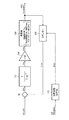
図1に、本実施形態の回路装置の構成例を示す。回路装置20は、物理量トランスデューサー12を駆動する駆動回路30と、駆動回路30からの信号を基準クロック信号CKFとしてクロック信号OSQを生成するFLL(Frequency Locked Loop)回路130と、物理量トランスデューサー12からの検出信号TQの検出処理を行う検出回路60と、を含む。
1. Configuration Example of Circuit Device FIG. 1 shows a configuration example of a circuit device according to this embodiment. The
FLL回路130は、基準クロック信号CKFに対する周波数比(逓倍率)を一定に保った(ロックした)クロック信号OSQを生成する回路である。クロック信号OSQの位相は基準クロック信号CKFの位相に同期しなくてもよい。FLL回路130は、基準クロック信号CKFとクロック信号OSQの周波数を比較する周波数比較器132と、その周波数比較器132の出力値QFD(出力信号)に対応する周波数で発振する発振器134と、を有する。このフィードバックループにより、基準クロック信号CKFとクロック信号OSQの周波数比がロックされる。なお、基準クロック信号CKFは、駆動回路30内の信号に基づいて生成されるクロック信号であり、例えば物理量トランスデューサー12の駆動周波数と同じ又は2倍の周波数のクロック信号である。
The
検出回路60は、クロック信号OSQに基づいて動作する回路を有する。即ち、駆動回路30からの基準クロック信号CKFに対して周波数比が一定に保たれたクロック信号OSQに基づいて、その回路は動作する。
The
検出回路60には、駆動信号の周波数成分を含む物理量トランスデューサー12からの検出信号TQが入力される。即ち、クロック信号OSQに基づいて動作する回路は、駆動信号の周波数成分を含む信号を処理する。本実施形態によれば、クロック信号OSQと駆動信号の周波数比をFLL回路130により一定に保つことができるので、駆動周波数成分が検出回路に対して影響を及ぼすことによって発生する検出性能の劣化を低減できる。この点について、以下に詳細に説明する。
The
本実施形態の検出回路60は、クロック信号OSQに基づいて動作する回路として、A/D変換回路及びデジタル信号処理部の少なくとも一方を有する。なお、以下では検出回路60がA/D変換回路及びデジタル信号処理部を含む場合を例に説明するが、いずれか一方を含まない場合にも本発明を適用できる。
The
従来は、これらの回路を、物理量トランスデューサー12を駆動する駆動回路30の駆動信号に基づく信号により動作させているが、駆動信号の駆動周波数はそれほど高くない(例えば50〜150kHz)。このため、A/D変換回路やデジタル信号処理部などの物理量の検出用の回路の高速動作の実現が難しいという問題がある。
Conventionally, these circuits, but are operated by a signal based on the driving signal of the driving
この問題を解決する手法として、発振回路を有するクロック信号生成回路を回路装置に設け、このクロック信号生成回路により高速のクロック信号を生成する手法を採用したとする。図2に、この場合の回路装置の比較構成例を示す。図2は、物理量トランスデューサーが振動片10(角速度センサー素子)である場合の比較構成例である。 As a technique for solving this problem, it is assumed that a clock signal generation circuit having an oscillation circuit is provided in a circuit device, and a high-speed clock signal is generated by the clock signal generation circuit. FIG. 2 shows a comparative configuration example of the circuit device in this case. FIG. 2 is a comparative configuration example in the case where the physical quantity transducer is the resonator element 10 (angular velocity sensor element).
この回路装置20は、駆動回路30、検出回路60、クロック信号生成回路70を含む。検出回路60は、振動片10からの検出信号IQを増幅する増幅回路61と、駆動回路30からの同期信号SYCにより増幅回路61からの信号を同期検波する同期検波回路81と、同期検波回路81からの信号をローパスフィルター処理するフィルター部90と、フィルター部90からの信号をA/D変換するA/D変換回路100と、A/D変換回路100からの信号をデジタル処理して角速度情報を出力するDSP部110(デジタル信号処理部)と、を含む。
The
DSP部110には、クロック信号生成回路70が生成したマスタークロック信号MCKが入力され、そのマスタークロック信号MCKに基づいてDSP部110が動作する。また、DSP部110は、マスタークロック信号MCKを分周してA/D変換用のクロック信号CKADを生成し、そのクロック信号CKADに基づいてA/D変換回路100がA/D変換動作を行う。
The
クロック信号生成回路70は、それに含まれる発振回路によりマスタークロック信号MCKを生成するので、振動片10の駆動周波数よりも高い周波数のマスタークロック信号MCKを出力できる。これにより、A/D変換回路100やDSP部110を高速動作させることが可能になる。
Since the clock
しかしながら、発振回路の発振周波数は、例えば温度依存性や製造ばらつき等の種々の要因によって変動する。例えば、発振回路としてCR発振器を想定できるが、CR発振器は、それを構成するキャパシターや抵抗、トランジスターの温度特性や製造ばらつきによって、発振周波数が一定ではない。このような発振周波数の変動が生じた場合、マスタークロック信号MCKと駆動信号の周波数比も変動することになり、駆動信号の周波数とA/D変換回路100やDSP部110の動作周波数との干渉を原因とする角速度コードのばらつきの問題が発生する可能性がある。
However, the oscillation frequency of the oscillation circuit varies due to various factors such as temperature dependence and manufacturing variations. For example, a CR oscillator can be assumed as the oscillation circuit, but the oscillation frequency of the CR oscillator is not constant due to the capacitor, resistance, transistor temperature characteristics, and manufacturing variations. When such a variation in the oscillation frequency occurs, the frequency ratio between the master clock signal MCK and the drive signal also varies, and interference between the frequency of the drive signal and the operating frequency of the A /
図3は、干渉周波数についての説明図である。図3の横軸は発振周波数であり、縦軸は角速度コードばらつきの大きさを示したものである。 FIG. 3 is an explanatory diagram of the interference frequency. In FIG. 3, the horizontal axis represents the oscillation frequency, and the vertical axis represents the magnitude of the angular velocity code variation.
クロック信号生成回路70に含まれる発振回路の発振周波数をfosとし、i、j、kを1以上の整数とし、サンプリングクロック信号等の動作用信号の周波数をfsm=fos/iとし、駆動信号の周波数をFRとする。i≧2の場合は、iはクロック信号の分周比に相当し、fos/iは、分周比iで分周されたサンプリングクロック信号等の動作用信号の周波数になる。
The oscillation frequency of the oscillation circuit included in the clock
この場合に干渉周波数はj×FR=k×fos/iが成り立つときの発振周波数である。即ち、干渉周波数をfinとすると、fos=finの場合に、j×FR=k×fos/iの関係式が成り立つ。 In this case, the interference frequency is an oscillation frequency when j × FR = k × fos / i. That is, assuming that the interference frequency is fin, the relational expression j × FR = k × fos / i holds when fos = fin.
例えば図3のI1に示す干渉周波数では、1×FR=fsm=fos/iが成り立っている。例えばI1の干渉周波数をfos=fin1とすると、1×FR=fos/i=fin1/iが成り立つ。これはj×FR=k×fos/iの関係式(干渉条件)において、j=1、k=1の場合に相当する。 For example, 1 × FR = fsm = fos / i is established at the interference frequency indicated by I1 in FIG. For example, if the interference frequency of I1 is fos = fin1, 1 × FR = fos / i = fin1 / i holds. This corresponds to the case where j = 1 and k = 1 in the relational expression (interference condition) of j × FR = k × fos / i.
またI2に示す干渉周波数では、2×FR=fsm=fos/iが成り立っている。例えばI2に示す干渉周波数をfos=fin2とすると、2×FR=fos/i=fin2/iが成り立つ。これはj×FR=k×fos/iの関係式において、j=2、k=1の場合に相当する。 Further, at the interference frequency indicated by I2, 2 × FR = fsm = fos / i is established. For example, when the interference frequency indicated by I2 is fos = fin2, 2 × FR = fos / i = fin2 / i holds. This corresponds to the case where j = 2 and k = 1 in the relational expression j × FR = k × fos / i.
またI3に示す干渉周波数では、3×FR=fsm=fos/iが成り立っている。例えばI3に示す干渉周波数をfos=fin3とすると、3×FR=fos/i=fin3/iが成り立つ。これはj×FR=k×fos/iの関係式において、j=3、k=1の場合に相当する。 Further, at the interference frequency indicated by I3, 3 × FR = fsm = fos / i is established. For example, assuming that the interference frequency indicated by I3 is fos = fin3, 3 × FR = fos / i = fin3 / i holds. This corresponds to the case where j = 3 and k = 1 in the relational expression j × FR = k × fos / i.
I4に示す干渉周波数では、3×FR=2×fsm=2×fos/iが成り立っている。例えばI4に示す干渉周波数をfos=fin4とすると、3×FR=2×fos/i=2×fin4/iが成り立つ。これはj×FR=k×fos/iの関係式において、j=3、k=2の場合に相当する。 At the interference frequency indicated by I4, 3 × FR = 2 × fsm = 2 × fos / i is established. For example, if the interference frequency indicated by I4 is fos = fin4, 3 × FR = 2 × fos / i = 2 × fin4 / i is established. This corresponds to the case where j = 3 and k = 2 in the relational expression j × FR = k × fos / i.
I5に示す干渉周波数では、5×FR=2×fsm=2×fos/iが成り立っている。例えばI5に示す干渉周波数をfos=fin5とすると、5×FR=2×fos/i=2×fin5/iが成り立つ。これはj×FR=k×fos/iの関係式において、j=5、k=2の場合に相当する。 At the interference frequency indicated by I5, 5 × FR = 2 × fsm = 2 × fos / i is established. For example, assuming that the interference frequency indicated by I5 is fos = fin5, 5 × FR = 2 × fos / i = 2 × fin5 / i is established. This corresponds to the case where j = 5 and k = 2 in the relational expression j × FR = k × fos / i.
このように干渉周波数においては、j×FR=k×fsm=k×fos/iの関係式で表される干渉条件が成り立つ。ここで、j×FRは、駆動周波数FRの高調波成分(j≧2)や基本波成分(j=1)に相当する。またfsm=fos/iは、A/D変換回路100のサンプリング周波数(広義には動作用信号の周波数)である。従って、干渉条件であるj×FR=k×fos/iは、駆動周波数FRの高調波成分(j≧2)や基本波成分(j=1)が、サンプリング周波数fos/iのk倍に一致するという条件になる。 Thus, at the interference frequency, the interference condition represented by the relational expression of j × FR = k × fsm = k × fos / i is satisfied. Here, j × FR corresponds to a harmonic component (j ≧ 2) or a fundamental component (j = 1) of the drive frequency FR. Fsm = fos / i is a sampling frequency of the A / D conversion circuit 100 (frequency of the operation signal in a broad sense). Therefore, the interference condition j × FR = k × fos / i is such that the harmonic component (j ≧ 2) and the fundamental component (j = 1) of the drive frequency FR are equal to k times the sampling frequency fos / i. It becomes a condition to do.
なお、図3に示す干渉周波数での角速度コードばらつきは、A/D変換回路100の入力信号に混入した不要信号の周波数成分(駆動周波数成分)が、A/D変換回路100のサンプリング動作により、信号帯域に折り返すことなどが原因で発生する。従って、干渉周波数での角速度コードばらつきは、実際には、j×FRとk×fsmとが完全に一致する場合ではなく、j×FRとk×fsmの周波数差Δfが十分に小さい場合に、顕著に現れる。具体的には、周波数差Δfが、所望信号の周波数帯域である信号帯域の周波数(例えば200Hz〜10Hz)よりも低い場合には、周波数差Δfによる折り返しノイズが信号帯域に現れるため、角速度コードばらつき(揺れ)の問題が生じることになる。周波数差Δfが大きい場合には、DSP部110の帯域制限用のローパスフィルターにより、折り返しノイズは十分に低減されるため、角速度コードばらつきも発生しないようになる。このように、本実施形態において避けるべき干渉周波数は、所与の周波数幅(信号帯域幅、Δf)を有するものと言うことができる。
Note that the angular velocity code variation at the interference frequency shown in FIG. 3 is that the frequency component (drive frequency component) of the unnecessary signal mixed in the input signal of the A /
本実施形態では、FLL回路130が出力するクロック信号OSQの周波数を、このような干渉周波数を避けた周波数に設定する手法を採用している。即ち、クロック信号OSQの周波数をFVとし、i、jを1以上の整数とし、動作用信号の周波数をFV/iとした場合に、j×FR≠FV/iとなるようにクロック信号OSQの周波数FVを設定する。動作用信号の周波数FV/iは、A/D変換回路100のサンプリングクロック信号やDSP部110の動作クロック信号(出力データレート)の周波数である。
In the present embodiment, a method is adopted in which the frequency of the clock signal OSQ output from the
具体的には、図4等で後述するFLL回路130の構成例において、比較器131に入力される基準値をSCとし、分周回路133の分周比をDRとする場合に、FV=(SC/DR)×FRが成り立つ。この場合に、j×FR≠FV/iとなるようにSC/DRを設定する(SC/DR≠j×i)ことで、クロック信号OSQの周波数FVを、干渉周波数を避けた周波数に設定する。
Specifically, in the configuration example of the
このように、j×FR≠FV/iとなるように周波数FVを設定すれば、図3のI1、I2、I3に示す干渉周波数(j×FR=1×fos/i)を避けた周波数に、周波数FVを設定できるようになる。従って、I1、I2、I3に示す大きな値の角速度コードばらつきの発生を低減できるようになり、検出性能の劣化を低減できる。 In this way, if the frequency FV is set so that j × FR ≠ FV / i, interference frequencies (j × FR = 1 × fos / i) indicated by I1, I2, and I3 in FIG. 3 are avoided. The frequency FV can be set. Accordingly, it is possible to reduce the occurrence of large values of angular velocity code variations indicated by I1, I2, and I3, and to reduce the degradation of detection performance.
更に本実施形態では、kを1以上の整数とした場合に、j×FR≠k×FV/iとなるように周波数FVを設定することが望ましい。即ち、図3のI1、I2、I3に示すようなk=1の場合の干渉周波数のみならず、I4、I5に示すようなk≧2の場合の干渉周波数(j×FR=k×fos/i)についても避けた周波数に、周波数FVを設定する。このようにすれば、I1、I2、I3に示すような大きな値の角速度コードばらつきの発生のみならず、I4、I5に示すような比較的小さな値の角速度コードばらつきの発生についても防止できるようになる。 Furthermore, in the present embodiment, it is desirable to set the frequency FV so that j × FR ≠ k × FV / i when k is an integer of 1 or more. That is, not only the interference frequency when k = 1 as shown by I1, I2, and I3 in FIG. 3, but also the interference frequency when j ≧ 2 as shown by I4 and I5 (j × FR = k × fos / The frequency FV is set to a frequency that is also avoided for i). In this way, it is possible to prevent not only the occurrence of large values of angular velocity code variations as indicated by I1, I2, and I3, but also the occurrence of relatively small values of angular velocity code variations as indicated by I4 and I5. Become.
なお、以上で説明したように、FLL回路130の発振周波数が干渉周波数を避けていればよいので、基準クロック信号CKFとクロック信号OSQの位相はロック(同期)される必要はない。即ち、周波数比較器45は周波数の比較ができる回路であればよく、位相の比較を行わなくてよい。そして、FLL回路130は、基準クロック信号CKFとクロック信号OSQの周波数比をロックできる回路であればよい。
As described above, since the oscillation frequency of the
2.FLL回路の第1の構成例
図4に、本実施形態のFLL回路の第1の構成例を示す。このFLL回路130は、周波数比較器132、ループフィルター136、発振器134を含む。周波数比較器132は、比較器131、分周回路133、カウンター135を含む。
2. First Configuration Example of FLL Circuit FIG. 4 shows a first configuration example of the FLL circuit of this embodiment. The
分周回路133は、駆動回路30からの基準クロック信号CKFを分周する。比較器131は、分周回路133からの分周クロック信号DVQと発振器134からのクロック信号OSQとに基づく比較対象値CTQと、比較対象値CTQの基準値SCとの比較処理を行う。カウンター135は、分周クロック信号DVQで規定される計測期間を、クロック信号OSQによってカウントすることで計測されたカウント値を、比較対象値CTQとして出力する。
The
具体的には、分周クロック信号DVQの周期が計測期間であり、その計測期間においてカウンター135がクロック信号OSQをカウントし、計測期間が終了したときのカウント値を比較対象値CTQとして出力する。比較器131は、比較対象値CTQと基準値SCとの差分に基づく出力値QFDを出力する。周波数比較器132と発振器134の間に設けられるループフィルター136は、出力値QFDをフィルター処理(例えば、積分処理、ローパスフィルター処理等)して発振周波数設定値TRM(トリミング値)を出力する。発振器134は、その周波数比較器132の出力値QFDに基づく発振周波数設定値TRMが設定され、その発振周波数設定値TRMに基づいて発振する。即ち、発振周波数設定値TRMは、所定範囲内で複数の値をとり得る設定値であり、その設定値に応じて発振器134の発振周波数が変化するように発振器134が構成される。
Specifically, the period of the divided clock signal DVQ is the measurement period, and the
比較対象値CTQと基準値SCがずれている場合、出力値QFDが変化し、発振周波数設定値TRMが変化し、クロック信号OSQの周波数が変化し、比較対象値CTQが変化する。このようなフィードバック制御により発振器134の発振周波数が制御され、駆動回路30からの基準クロック信号CKFの周波数に対して周波数比が一定に保たれる。
When the comparison target value CTQ and the reference value SC are different, the output value QFD changes, the oscillation frequency setting value TRM changes, the frequency of the clock signal OSQ changes, and the comparison target value CTQ changes. By such feedback control, the oscillation frequency of the
以上の第1の構成例では、周波数比較器132とループフィルター136をロジック回路(デジタル回路)により構成することが可能である。発振器134を除く部分をロジック回路で構成できることで、アナログ回路で構成する場合に比べて回路の簡素化や面積削減等を実現できる。
In the above first configuration example, the
3.FLL回路の第2の構成例
図5に、本実施形態のFLL回路の第2の構成例を示す。このFLL回路130は、周波数比較器132、ループフィルター136、発振器134を含む。周波数比較器132は、比較器131、分周回路133、カウンター135を含む。ループフィルター136は、積分器137、ゲイン処理部139を含む。なお以下では、既に説明した構成要素と同一の構成要素については同一の符号を付し、適宜説明を省略する。
3. Second Configuration Example of FLL Circuit FIG. 5 shows a second configuration example of the FLL circuit of this embodiment. The
比較器131は差分器であり、カウンター135からの比較対象値CTQと基準値SCとの差分処理を行い、その差分処理で求めた差分値QFDを出力する。
The
積分器137は、周波数比較器132の出力(差分値QFD)を積分し、その積分で求めた積分値ITQを出力する。具体的には、積分器137は、積分値ITQを分周クロック信号DVQの1周期分遅延させる遅延回路46(例えばラッチ回路等)と、遅延回路46の出力と積分値ITQとを加算処理する加算器44と、を含む。加算器44の出力が積分値ITQとなる。
The
ゲイン処理部139は、積分器137の出力(積分値ITQ)にゲイン処理を行い、そのゲイン処理された値を発振周波数設定値TRMとして出力する。ゲイン処理は、積分値ITQに対してゲインを乗算する処理である。
The
さて、発振器134はデジタルの発振周波数設定値TRMに応じて離散的な発振周波数で発振する。そのため、発振周波数設定値TRMが一定になってしまうと、離散的な発振周波数のいずれかに固定されてしまい、駆動周波数に対して所望の周波数比のクロック信号OSQが得られない(周波数比に誤差が生じる)。この点、本実施形態によれば、FLL回路130のループに比較器131(差分器)と積分器137を設けることで、クロック信号OSQの周波数をデルタシグマ変調できる。即ち、クロック信号OSQの周波数が変調により時系列で変化し、その平均の周波数として、駆動周波数に対して所望の周波数比のクロック信号OSQを得ることができる。
The
以下、上記構成例の動作の詳細について説明する。図6に、図5のFLL回路130の伝達関数を説明する図を示す。
Details of the operation of the above configuration example will be described below. FIG. 6 is a diagram illustrating the transfer function of the
図6の等価回路図には、各構成要素の伝達関数を記載している。SCは基準値であり、等価回路の入力である。gは積分値に乗算されるゲインである。Qは発振器134を量子化器とみなした場合の量子化ノイズである。HD2Fは、デジタル値である発振周波数設定値を発振器134の発振周波数FVに変換する係数である。例えば十進数のデジタル値10を周波数200kHzに変換する場合、HD2F=200kHz/10=20kHzである。発振周波数FVは、等価回路の出力である。HF2Dは、発振器134の発振周波数FVをカウンター135のカウント値(比較対象値)に変換する係数である。例えば周波数200kHzをカウント値2000に変換する場合、HF2D=2000/200kHz=10ms(100Hz)である。この値は、カウンター135での計測期間に対応する。カウンター135は計測期間が終了した後に、その計測期間でカウントしたカウント値を出力するので、ループから見ると1周期前のカウント値になる。そのため、カウンター135の等価回路として遅延回路(z−1)が含まれる。
In the equivalent circuit diagram of FIG. 6, the transfer function of each component is described. SC is a reference value and is an input of an equivalent circuit. g is a gain multiplied by the integral value. Q is quantization noise when the
上記の等価回路から、FLL回路130の伝達関数STF=FV/SCは式FAとなる。この伝達関数STFはローパス特性であり、そのDC特性STFDC(ω=0のときの伝達関数STF)は式FBとなる。またFLL回路130のノイズ伝達関数NTF=FV/Qは式FCとなる。このノイズ伝達関数NTFはハイパス特性であり、低周波数でのノイズが小さいことが分かる。即ち、発振周波数FVを時間的に平均した場合、量子化ノイズが低減されている。
From the above equivalent circuit, the transfer function STF = FV / SC of the
分周回路133の分周比をDRとし、駆動回路30からの基準クロック信号CKFの周波数をFRとした場合、カウンター135での計測期間は1/(FR/DR)=DR/FRなので、HF2D=DR/FRとなる。式FBより、DC特性はSTFDC=FV/SC=1/HF2Dなので、FV/SC=FR/DRとなり、FV=(SC/DR)×FRとなる。即ち、FLL回路130が生成するクロック信号OSQの周波数FVと、駆動回路30からの基準クロック信号CKFの周波数FRとの比は、SC/DRである。
When the frequency dividing ratio of the
図3で説明したように、干渉周波数はj×FR=k×fos/iが成り立つ発振周波数fosである。本実施形態では、この干渉周波数を避けるためにクロック信号OSQの周波数FVをj×FR≠k×FV/iが成り立つように設定する。即ち、FV/FR=SC/DR≠(j×i)/kに設定する。 As described with reference to FIG. 3, the interference frequency is the oscillation frequency fos where j × FR = k × fos / i. In the present embodiment, in order to avoid this interference frequency, the frequency FV of the clock signal OSQ is set so that j × FR ≠ k × FV / i. That is, FV / FR = SC / DR ≠ (j × i) / k is set.
k=1の場合には(j×i)/kは1以上の整数となり、k≧2の場合には(j×i)/kは分数(小数)又は1以上の整数となる。このため、本実施形態ではSC/DRを小数に設定する。これにより、少なくともk=1の場合の干渉周波数と、k≧2の場合において(j×i)/kが整数となる場合の干渉周波数を避けることができる。また、(j×i)/kが分数の場合であっても、その分数を避けてSC/DRを設定することで、干渉周波数を避けることができる。 In the case of k = 1, (j × i) / k is an integer of 1 or more, and in the case of k ≧ 2, (j × i) / k is a fraction (decimal number) or an integer of 1 or more. For this reason, in this embodiment, SC / DR is set to a decimal. Thereby, at least the interference frequency when k = 1 and the interference frequency when (j × i) / k becomes an integer when k ≧ 2 can be avoided. Even when (j × i) / k is a fraction, interference frequency can be avoided by setting SC / DR while avoiding the fraction.
また本実施形態では、基準値SCを小数に設定してもよい。この場合、分周比DRが小さくてもSC/DRを任意の小数に設定できる。即ち、比較器131による比較の周期(計測期間)を短くしたい場合には分周比DRを小さくする必要がある。例えば基準値SCを整数とし、分周比をDR=3とした場合、SC/DRの整数部を除く小数部は0.333・・・又は0.666・・・となり、小数としてとり得る選択肢が少なくなる。この点、基準値SCを小数に設定することで、SC/DRを任意の小数に設定できる。
In the present embodiment, the reference value SC may be set to a decimal number. In this case, the SC / DR can be set to an arbitrary decimal number even if the frequency division ratio DR is small. That is, in order to shorten the comparison period (measurement period) by the
なお、上述したパラメーター(基準値SC、分周比DR、ゲイン処理部139のゲイン)は、例えば外部の処理部(例えば図18の処理部520)から回路装置20のレジスター部(例えば図18のレジスター部142)に書き込まれる構成としてもよい。
The parameters described above (reference value SC, frequency division ratio DR, gain of gain processing unit 139) are, for example, from an external processing unit (for example, processing
図7に、FLL回路130の設定パラメーターの第1の例を示し、図8(A)〜図9に、その設定パラメーターでの動作波形例を示す。
FIG. 7 shows a first example of setting parameters of the
図7に示すように、基準値をSC=16とし、ゲインを1とし、基準クロック信号CKFの周波数をFR=50kHzとし、分周比をDR=4とする。発振周波数設定値TRMは0〜15の16階調であり、発振周波数FVの1階調のステップが2kHzであり、TRM=8のときに発振周波数FV=200kHzであるとする。この場合、DC特性としては、FV=(SC/DR)×FR=200kHzとなる。 As shown in FIG. 7, the reference value is SC = 16, the gain is 1, the frequency of the reference clock signal CKF is FR = 50 kHz, and the frequency division ratio is DR = 4. The oscillation frequency setting value TRM has 16 gradations from 0 to 15, the step of one gradation of the oscillation frequency FV is 2 kHz, and the oscillation frequency FV = 200 kHz when TRM = 8. In this case, the DC characteristic is FV = (SC / DR) × FR = 200 kHz.
動作開始からの時系列の変化は以下のようになる。図8(A)に示すように、積分器137の出力(積分値ITQ)の初期値を例えば0とする。このとき、図8(B)に示すように発振周波数設定値TRM=0となるので図8(D)に示すように発振周波数はFV=184kHzから始まる。ターゲットの200kHzよりも発振周波数FVが低いので、カウント値(比較対象値CTQ)は基準値SC=16よりも小さくなり、差分値QFD>0となる。そのため積分値ITQが増加し、発振周波数設定値TRMが増加し、発振周波数FVが上昇する。これを繰り返してターゲットであるFV=200kHzに到達する。
The time series change from the start of operation is as follows. As shown in FIG. 8A, the initial value of the output (integrated value ITQ) of the
図9は、上記の時系列変化に対応するタイミングチャートである。図9に示すように、カウンター135は、分周クロック信号DVQの立ち上がりでカウント値を出力する。即ち、分周クロック信号DVQの立ち上がりでカウンター135がリセットされ、そのリセットされたタイミングから次にリセットされるタイミングまでを計測期間としてクロック信号OSQをカウントし、そのカウント値を比較対象値CTQとして出力する。
FIG. 9 is a timing chart corresponding to the above time-series change. As shown in FIG. 9, the
差分器42と積分器137とゲイン処理部139は、分周クロック信号DVQの立ち上がりに同期して動作する。即ち、差分器42は、分周クロック信号DVQの立ち上がりで基準値SCと比較対象値CTQの差分値QFDを出力する。積分器137は、分周クロック信号DVQの立ち上がりで遅延回路(z−1)が動作し、積分値ITQを更新する。ゲイン処理部139は、分周クロック信号DVQの各立ち上がりで発振周波数設定値TRMを出力する。
The
比較対象値CTQ(カウント値)、積分値ITQ、発振周波数設定値TRMのタイミングチャートに記載された数値は、図8(C)、図8(A)、図8(B)の波形に対応している。発振周波数設定値TRMが初期値であるTRM=0から、ターゲットの200kHzに対応するTRM=8に漸近していくことが分かる。
The numerical values described in the timing chart of the comparison target value CTQ (count value), the integral value ITQ, and the oscillation frequency setting value TRM correspond to the waveforms in FIGS. 8C, 8A, and 8B. ing. It can be seen that the oscillation frequency setting value TRM gradually approaches TRM = 8 corresponding to the
図10に、FLL回路130の設定パラメーターの第2の例を示し、図11(A)〜図11(C)に、その設定パラメーターでの動作波形例を示す。第2の例は、発振周波数FVの階調の中に、ターゲットと同一の周波数が含まれない場合の例である。
FIG. 10 shows a second example of setting parameters of the
図10に示すように、基準値をSC=320とし、ゲインを1/32とし、基準クロック信号CKFの周波数をFR=50kHzとし、分周比をDR=32とする。発振周波数設定値TRMは0〜15の16階調であり、発振周波数FVの1階調のステップが1kHzであり、TRM=8のときに発振周波数FV=498.2kHzであるとする。この場合、DC特性としては、FV=(SC/DR)×FR=500kHzとなる。 As shown in FIG. 10, the reference value is SC = 320, the gain is 1/32, the frequency of the reference clock signal CKF is FR = 50 kHz, and the frequency division ratio is DR = 32. The oscillation frequency setting value TRM has 16 gradations of 0 to 15, and the gradation step of one gradation of the oscillation frequency FV is 1 kHz. When TRM = 8, the oscillation frequency FV = 498.2 kHz. In this case, the DC characteristic is FV = (SC / DR) × FR = 500 kHz.
図11(A)〜図11(C)に示すように、動作開始からの時系列において発振周波数FVがターゲット500kHzに漸近していくことは、上述した第1の例と同様である。第2の例では、ターゲット500kHzに近づいた後は発振周波数FVが一定ではなく、デルタシグマ変調により変動する。即ち、TRM=9でFV=499.2kHz、TRM=10でFV=500.2kHzなので、平均として500kHzとなるようにデルタシグマ変調によりTRM=9、10を行ったり来たりする。 As shown in FIGS. 11A to 11C, the oscillation frequency FV gradually approaches the target 500 kHz in the time series from the start of the operation, as in the first example described above. In the second example, after approaching the target 500 kHz, the oscillation frequency FV is not constant and varies due to delta-sigma modulation. That is, since TRM = 9 and FV = 499.2 kHz, and TRM = 10 and FV = 500.2 kHz, TRM = 9 and 10 are moved back and forth by delta-sigma modulation so that the average is 500 kHz.
図12に、FLL回路130の設定パラメーターの第3の例を示す。第3の例は、SC/DRを小数に設定する場合の例である。
FIG. 12 shows a third example of setting parameters of the
図12に示すように、基準値をSC=40.4とし、ゲインを1/40.4とし、基準クロック信号CKFの周波数をFR=50kHzとし、分周比をDR=4とする。発振器134のモデルは図10と同様であるとする。周波数設定値TRMは0〜15の16階調であり、発振周波数FVの1階調のステップが1kHzであり、TRM=8のときに発振周波数FV=503.2kHzであるとする。この場合、DC特性としては、FV=(SC/DR)×FR=505kHzとなる。
As shown in FIG. 12, the reference value is SC = 40.4, the gain is 1 / 40.4, the frequency of the reference clock signal CKF is FR = 50 kHz, and the frequency division ratio is DR = 4. Assume that the model of the
4.発振器
以下、発振器134がCR発振回路である場合を例にとって、発振器134の詳細について説明する。
4). Oscillator The details of the
本実施形態のCR発振回路は、可変容量回路及び可変抵抗回路の少なくとも一方を有する。そして、発振周波数設定値TRMに応じて可変容量回路の容量値又は可変抵抗回路の抵抗値が設定されることで、CR発振回路の発振周波数FVが設定される。 The CR oscillation circuit of this embodiment has at least one of a variable capacitance circuit and a variable resistance circuit. Then, the oscillation frequency FV of the CR oscillation circuit is set by setting the capacitance value of the variable capacitance circuit or the resistance value of the variable resistance circuit according to the oscillation frequency setting value TRM.
図13に、この場合の発振器134の詳細な構成例を示す。発振器134であるCR発振回路は、キャパシターCと、可変抵抗回路196(第1の周波数調整部)と、可変容量回路197(第2の周波数調整部)と、増幅回路180(バッファー回路)を有する。
FIG. 13 shows a detailed configuration example of the
CR発振回路は、電源電圧VDOSが供給されて動作して、クロック信号OSQ(発振信号)を生成する。具体的にはCR発振回路は、キャパシターと抵抗で構成されるRC回路を用いて、信号を入力に帰還して発振信号を生成する。そして、生成された発振信号を波形整形した信号がクロック信号OSQとして出力される。 The CR oscillation circuit operates by being supplied with the power supply voltage VDOS, and generates a clock signal OSQ (oscillation signal). Specifically, the CR oscillation circuit generates an oscillation signal by feeding back a signal to an input using an RC circuit composed of a capacitor and a resistor. Then, a waveform-shaped signal of the generated oscillation signal is output as the clock signal OSQ.
増幅回路180(反転増幅回路)はインバーター回路IV0、IV1、IV2を有する。インバーター回路IV1の出力は、キャパシターCを介して、増幅回路180の入力ノードNIに帰還される。インバーター回路IV2の出力は、可変抵抗回路196(R)を介して、増幅回路180の入力ノードNIに帰還される。インバーター回路IV0の入力が増幅回路180の入力になる。
The amplifier circuit 180 (inverting amplifier circuit) includes inverter circuits IV0, IV1, and IV2. The output of the inverter circuit IV1 is fed back to the input node NI of the
インバーター回路IV2から出力される発振信号はインバーター回路IV3により波形整形されて、矩形波のクロック信号OSQとして出力される。なお、インバーター回路IV3の後段に分周回路を設け、クロック信号OSQを分周することで得られた1又は複数のクロック信号を出力するようにしてもよい。 The oscillation signal output from the inverter circuit IV2 is waveform-shaped by the inverter circuit IV3 and output as a rectangular wave clock signal OSQ. Note that a frequency dividing circuit may be provided at the subsequent stage of the inverter circuit IV3, and one or a plurality of clock signals obtained by dividing the clock signal OSQ may be output.
この構成例では、物理量トランスデューサー12と回路装置20とが接続され、FLL回路130が動作する状態において、発振周波数設定値TRMに基づいて可変容量回路197の容量値が設定される。これにより、CR発振回路の発振周波数がFLL回路130のループにより制御される。可変容量回路197は、その容量値が可変に調整可能な回路になっており、可変容量回路197の容量値を変化させることで、RC回路の容量値が変化して、CR発振回路の発振周波数が設定される。
In this configuration example, when the
一方、物理量トランスデューサー12と回路装置20とが接続される前において、CR発振回路の発振周波数が、可変抵抗回路196により調整される。このとき、CR発振回路の発振周波数は、ターゲットの発振周波数(干渉周波数を避けた周波数)の近傍に調整される。即ち、発振周波数設定値TRMにより設定できる発振周波数の範囲に、ターゲットの発振周波数(干渉周波数を避けた周波数)が入るように、可変抵抗回路196の抵抗値が調整される。可変抵抗回路196は、その抵抗値が可変に調整可能な回路になっており、可変抵抗回路196の抵抗値を変化させることで、RC回路の抵抗値が変化して、CR発振回路の発振周波数が設定される。
On the other hand, before the
このようにすることで、本実施形態では、物理量トランスデューサー12と回路装置20とが接続される前の状態での、発振周波数の調整(粗調整)と、物理量トランスデューサー12と回路装置20とが接続された状態での、FLL回路130による発振周波数のロック(駆動周波数と発振周波数の比を一定に保つ制御)を実現できる。これにより、干渉周波数を避けた周波数のクロック信号OSQを生成することが可能になり、上述した干渉による検出性能の劣化を低減できる。
By doing in this way, in this embodiment, adjustment of the oscillation frequency (coarse adjustment) before the
なお、図13ではCR発振回路が可変容量回路197及び可変抵抗回路196の両方を含み、可変容量回路197の容量値が発振周波数設定値TRMに応じて設定される場合を例に説明したが、CR発振回路の構成はこれに限定されない。例えば、可変容量回路197及び可変抵抗回路196の一方を含まなくてもよい。或いは、可変抵抗回路196の抵抗値が発振周波数設定値TRMに応じて設定されることで、発振周波数が制御されてもよい。或いは、不図示の電圧生成回路を含み、その電圧生成回路が発振周波数設定値TRMに応じて電源電圧VDOSを変更することで、発振周波数が制御されてもよい。或いは、不図示の電圧生成回路を含み、その電圧生成回路が生成する電源電圧VDOSが粗調整されることで、発振周波数が粗調整されてもよい。
Although the CR oscillation circuit includes both the
図14に、CR発振回路を構成する増幅回路180、可変抵抗回路196及び可変容量回路197の詳細な構成例を示す。
FIG. 14 shows a detailed configuration example of the
増幅回路180は、NAND回路NA、インバーター回路IV1、IV2を有する。インバーター回路IV1の出力は、キャパシターCを介して、増幅回路180の入力ノードNIに帰還される。インバーター回路IV2の出力は、可変抵抗回路196を介して、増幅回路180の入力ノードNIに帰還される。NAND回路NAの第1の入力が、増幅回路180の入力になり、NAND回路NAの第2の入力にはイネーブル信号ENが入力される。イネーブル信号ENがHレベルになるとCR発振回路が動作イネーブル状態に設定され、イネーブル信号ENがLレベルになると動作ディスエーブル状態に設定される。
The
可変抵抗回路196は、直列接続される複数の抵抗素子R1〜R6と、複数の抵抗素子R1〜R6の各抵抗素子に対して各ヒューズ素子が並列に接続される複数のヒューズ素子FU1〜FU6(広義にはスイッチ素子)を有する。例えばヒューズ素子FU1は抵抗素子R1と並列に接続され、ヒューズ素子FU2は抵抗素子R2と並列に接続される。ヒューズ素子FU3〜FU6と抵抗素子R3〜R6の接続構成も同様である。また可変抵抗回路196は、複数の抵抗素子R1〜R6に直列接続される基準抵抗素子R7を有する。即ち、複数の抵抗素子R1〜R6及び基準抵抗素子R7は、増幅回路180の出力ノードNQと入力ノードNIとの間に直列接続される。
The
可変容量回路197は、可変容量素子CV1〜CV4と容量制御電圧出力回路BC1〜BC4を有する。可変容量素子CV1〜CV4の一端は、増幅回路180の出力ノードNQに接続され、他端は容量制御電圧出力回路BC1〜BC4の出力に接続されている。可変容量素子CV1〜CV4は、容量制御電圧出力回路BC1〜BC4が出力した容量制御電圧により容量が変化する素子である。容量制御電圧は、発振周波数設定値TRMに対応した電圧に設定される。可変容量素子CV1〜CV4は例えばバリキャップ(バラクター)などにより実現できる。可変容量回路197は、例えばバイナリーに重みづけられた可変容量素子のアレイにより実現することができ、この場合には容量制御電圧による制御はハイレベルとローレベルの2値制御になる。例えば、発振周波数設定値TRMが4ビットの場合、そのLSB側から第1〜第4のビットの論理レベルを、それぞれ容量制御電圧出力回路BC1〜BC4が出力する。
The
5.可変抵抗回路を用いた発振周波数の調整
次に可変抵抗回路196を用いた発振周波数の調整手法について説明する。発振周波数の調整については、半導体ウェハープロセスによるトランジスターや抵抗などの素子ばらつきに対して、可変抵抗回路196を用いて所望の発振周波数に調整することを目的としている。
5. Adjustment of Oscillation Frequency Using Variable Resistance Circuit Next, a method for adjusting the oscillation frequency using the
図14の可変抵抗回路196の抵抗素子R1〜R6の抵抗値は例えばバイナリーで重み付けされている。例えばR1〜R6の各抵抗素子は、1又は複数の抵抗ユニットにより構成されている。例えばR1は20=1個の抵抗ユニットで構成され、R2は直列接続された21=2個の抵抗ユニットにより構成され、R3は直列接続された22個の抵抗ユニットにより構成される。同様に、R4、R5、R6は、各々、直列接続された23個、24個、25個の抵抗ユニットにより構成される。従って、抵抗ユニットの抵抗値をRUとすると、R1の抵抗値は20×RU(=RU)、R2の抵抗値は21×RU(=2×RU)、R3の抵抗値は22×RU、R4の抵抗値は23×RU、R5の抵抗値は24×RU、R6の抵抗値は25×RUに設定される。
The resistance values of the resistance elements R1 to R6 of the
一方、R7は、基準となる発振周波数を設定するための基準抵抗素子であり、R7の抵抗値である基準抵抗値をRBとすると、RBは例えばR6と同程度の抵抗値に設定できる。このように設定することで、可変抵抗回路196の抵抗値を所定範囲内(例えばRB〜RB+RU×(26−1)の範囲)で可変に設定できるようになる。
On the other hand, R7 is a reference resistance element for setting a reference oscillation frequency. If the reference resistance value, which is the resistance value of R7, is RB, RB can be set to a resistance value comparable to R6, for example. With this setting, the resistance value of the
図14に示すように、FU1〜FU6の各ヒューズ素子は、R1〜R6の各抵抗素子と並列に設けられている。そしてヒューズカット前においては、全てのヒューズ素子FU1〜FU6が非カット状態となっている。従って、可変抵抗回路196の抵抗値は、R7の基準抵抗値RB(正確には、RB+ヒューズ素子等の寄生抵抗値)に設定される。そして、この状態でCR発振回路の発振周波数が計測される。計測された発振周波数をfrとすると、例えば下式(1)に示すようにfrの一次式で表されるトリミング式によりヒューズ値が計算される。なおa、bは定数である。
ヒューズ値=a×fr+b (1)
As shown in FIG. 14, the fuse elements FU1 to FU6 are provided in parallel with the resistance elements R1 to R6. Before the fuse is cut, all the fuse elements FU1 to FU6 are in an uncut state. Accordingly, the resistance value of the
Fuse value = a × fr + b (1)
計算されたヒューズ値に基づいて、ヒューズ素子FU1〜FU6のいずれをカット(トリミング)するかが決定される。例えばトリミング式で計算されたヒューズ値に基づいて、ヒューズ素子FU1、FU3、FU4、FU5がカットされたとする。この場合には、可変抵抗回路196の抵抗値は、RB+R1+R3+R4+R5(+寄生抵抗値)になる。
Based on the calculated fuse value, it is determined which of the fuse elements FU1 to FU6 is to be cut (trimmed). For example, it is assumed that the fuse elements FU1, FU3, FU4, and FU5 are cut based on the fuse value calculated by the trimming formula. In this case, the resistance value of the
具体的にはヒューズ値(整数に変換した後のヒューズ値)をバイナリー表現のデータに変換することで、カットするヒューズ素子を決定できる。例えばヒューズ値=1=20であれば、ヒューズ素子FU1をカットし、ヒューズ値=2=21であれば、ヒューズ素子FU2をカットする。また、ヒューズ値=3=20+21であれば、ヒューズ素子FU1及びFU2をカットし、ヒューズ値=4=22であれば、ヒューズ素子FU3をカットし、ヒューズ値=5=20+22であれば、ヒューズ素子FU1及びFU3をカットする。即ち、ヒューズ素子FU1がバイナリー表現のヒューズ値のLSBに相当し、ヒューズ素子FU2がLSBの次のビットに相当し、ヒューズ素子FU3がその次のビットに相当する。同様にヒューズ素子FU6はバイナリー表現のヒューズ値のMSBに相当する。そしてヒューズ値のLSBが1であれば、ヒューズ素子FU1をカットし、0であればカットしない。LSBの次のビットが1であれば、ヒューズ素子FU2をカットし、0であればカットしない。 Specifically, the fuse element to be cut can be determined by converting the fuse value (the fuse value after being converted into an integer) into binary representation data. For example, if the fuse value = 1 = 2 0 , the fuse element FU1 is cut, and if the fuse value = 2 = 2 1 , the fuse element FU2 is cut. If fuse value = 3 = 2 0 +2 1 , fuse elements FU1 and FU2 are cut. If fuse value = 4 = 2 2 , fuse element FU3 is cut and fuse value = 5 = 2 0 +2. If it is 2 , the fuse elements FU1 and FU3 are cut. That is, the fuse element FU1 corresponds to the LSB of the fuse value expressed in binary, the fuse element FU2 corresponds to the next bit of the LSB, and the fuse element FU3 corresponds to the next bit. Similarly, the fuse element FU6 corresponds to the MSB of the fuse value in binary representation. If the LSB of the fuse value is 1, the fuse element FU1 is cut, and if it is 0, it is not cut. If the next bit of the LSB is 1, the fuse element FU2 is cut, and if it is 0, it is not cut.
6.発振器の変形例
以上では発振器134がCR発振回路である場合を例に説明したが、発振器134はこの構成に限定されない。例えば、発振器134は、図15に示す構成であってもよい。
6). Modified Example of Oscillator In the above, the case where the
図15に示す発振器134は、発振周波数設定値TRMをD/A変換するD/A変換回路72と、D/A変換回路72からのアナログの出力電圧DAQに基づいて発振する電圧制御発振器74と、を含む。この発振器134を本実施形態のFLL回路130に適用した場合、発振周波数設定値TRMに応じてD/A変換回路72の出力電圧DAQが変化し、それに応じてクロック信号OSQの周波数が変化し、その周波数が周波数比較器132とループフィルター136を介して発振周波数設定値TRMにフィードバックされる。アナログの出力電圧DAQは離散的な電圧値をとるが、図5等で説明したようにデルタシグマ変調により平均として所望の周波数となるクロック信号OSQが出力される。
An
7.FLL回路の変形例
また以上ではFLL回路130の周波数比較器132とループフィルター136がロジック回路で構成される場合を例に説明したが、FLL回路130はこの構成に限定されない。例えば、図16に示すように、周波数比較器132やループフィルター136がアナログ回路で構成されてもよい。
7). Modification Example of FLL Circuit Further, the case where the
図16に示すFLL回路130は、周波数比較器45、ループフィルター43、発振器48、分周回路41を含む。
The
分周回路41は、クロック信号OSQを分周し、分周クロック信号DVOSを出力する。周波数比較器45は、基準クロック信号CKFの周波数と分周クロック信号DVOSの周波数を比較し、それらの差分に基づくアナログ信号QPを出力する。例えば周波数比較器45はチャージポンプ回路で実現される。ループフィルター43は、アナログ信号QPをローパスフィルター処理し、その処理で得られた電圧を制御電圧VLQとして出力する。例えばループフィルター136は、キャパシターや抵抗で構成されたパッシブローパスフィルターで実現される。発振器48は、制御電圧VLQに応じた周波数で発振し、クロック信号OSQを出力する。例えば発振器48は、電圧制御発振器(VCO)で実現される。
The
8.演算処理部
以上で説明したFLL回路130によれば、駆動回路30からの基準クロック信号CKFをSC/DR倍したクロック信号OSQ(又は、それを分周した動作クロック信号)でA/D変換回路100やDSP部110を動作させることが可能になる。
8). Arithmetic Processing Unit According to the
このとき、物理量トランスデューサー12の駆動周波数は製造ばらつき等により変動するため、その周波数の変動にともなってクロック信号OSQの周波数が変動する。例えばジャイロセンサーにおいて角度情報は角速度情報を積分することで求めるが、DSP部110等の動作周波数が変化することで積分期間が変わり、角速度情報に誤差が生じる可能性がある。
At this time, since the drive frequency of the
そこで本実施形態では、検出回路60の後段に設けられる演算処理部150が以下の処理を行うことで、より正確な角速度情報を求めることができる。なお、演算処理部150は検出回路60のDSP部110に含まれてもよい。
Therefore, in the present embodiment, more accurate angular velocity information can be obtained by the
図17に演算処理部150の構成例を示す。演算処理部150は、乗算処理部155、積分処理部156を含み、クロック信号OSQをDO分周した動作クロック信号で動作する(すなわち、基準クロック周波数FRをもちいて、(SC/DR)×FR/DOと表される周波数の動作クロック信号で動作する)。乗算処理部155は、検出回路60からの角速度情報QG(物理量情報)と、駆動回路30の駆動周波数に基づき値が設定される演算係数CF(広義には駆動周波数情報)とに基づく乗算処理を行う。積分処理部156は、乗算処理部155の乗算結果QM(例えば角度変位)を受けて、乗算結果QMについての積分処理を行う。これにより角速度情報QGの積分処理が実現される。そして積分処理部156は、回転数情報QHを出力する。この回転数情報QHは、固定小数点表現の整数部REVQと小数部DEGQを有する。
FIG. 17 shows a configuration example of the
演算係数CFは、後述するように駆動回路30の駆動周波数に基づき値が設定される係数となっている。更に具体的には、駆動周波数及び角速度情報の設定感度に基づき値が設定される係数となっている。乗算処理部155が、角速度情報QGに対して、このような演算係数CFを乗算する処理を行うことで、駆動回路30の駆動周波数により規定される時間間隔情報に基づく演算処理が実現される。
The calculation coefficient CF is a coefficient whose value is set based on the drive frequency of the
より具体的には、乗算処理部155は乗算器MLAを含む。この乗算処理部155は、角速度情報QG(ジャイロ信号)に対して演算係数CF(定数)を乗算する処理を行う。これによりデータレートの時間間隔での角度変位(Δθ)を算出する。この角度変位は、角速度と時間間隔との乗算処理により求められるものである。そして、時間間隔は、演算係数CFにより設定される。
More specifically, the
乗算処理部155に入力される演算係数CFは、例えば下式(2)のように表される。
CF=1/(360×SEN×fxt×(SC/DR)/DO) (2)
The arithmetic coefficient CF input to the
CF = 1 / (360 × SEN × fxt × (SC / DR) / DO) (2)
上式(2)において、SENは設定感度(LSB/dps)を表し、fxtは振動片10(水晶振動片)の駆動周波数(Hz)を表す。具体的には、設定感度SENは、物理量検出装置(ジャイロセンサー)の仕様(設計値)として設定される角速度の感度である。即ち、設定感度SENは、例えばSEN=300(LSB/dps)というように、製品の仕様として一意に決定されている。また、基準クロック信号として振動片10の駆動信号(又は、駆動信号に基づく信号)を用い、fxtは、回路装置20と振動片10を接続した状態で測定される駆動周波数である。即ち、fxtは駆動周波数の測定結果に基づき設定されるものである。なお演算係数CFは、上式(2)に限定されず、例えば上式(2)に所定の定数を乗算した係数などの種々の変形実施が可能である。
In the above equation (2), SEN represents the set sensitivity (LSB / dps), and fxt represents the drive frequency (Hz) of the resonator element 10 (crystal resonator element). Specifically, the set sensitivity SEN is an angular velocity sensitivity set as a specification (design value) of the physical quantity detection device (gyro sensor). That is, the set sensitivity SEN is uniquely determined as the product specification, for example, SEN = 300 (LSB / dps). Further, a drive signal (or a signal based on the drive signal) of the
このように本実施形態では、駆動回路30の駆動周波数(fxt)と角速度(物理量情報)の設定感度(SEN)に基づき値が設定される演算係数CFを用いて、演算処理部150の演算処理(乗算処理)が行われる。そして、この演算係数CFの設定に用いられる駆動周波数(fxt)は、駆動周波数の測定結果に基づき設定されるものである。具体的には、本実施形態では、上式(2)の演算係数CFが、駆動周波数情報(駆動周波数に基づきその値が設定される情報)として、不揮発性メモリー146に書き込まれる。そして演算処理部150は、不揮発性メモリー146から、駆動周波数情報として演算係数CFを読み出し、この駆動周波数情報により規定される時間間隔情報に基づいて、演算処理を行う。
As described above, in the present embodiment, the arithmetic processing of the
駆動回路30の駆動周波数には、設計値に対してバラツキが生じる。例えば駆動周波数の設計値(50kHz〜200kHz)に対してバラツキが発生する。そして本実施形態では、演算処理部150の演算処理における時間間隔情報は駆動周波数により規定されるため、駆動周波数にバラツキがあると、演算結果にもバラツキが発生してしまう。例えば、検出対象が実際には10度だけ回転しているのに、駆動周波数にバラツキがあると、演算処理部150の演算結果である回転角度は10度にはならず、10度からずれた角度になってしまう。
The drive frequency of the
この点、本実施形態では、振動片10と回路装置が接続された状態で駆動周波数が測定され、上式(2)に示すように、測定された駆動周波数(fxt)に基づき演算係数CF(広義には駆動周波数情報)が求められ、不揮発性メモリー146に記憶される。そして演算処理部150は、この不揮発性メモリー146から読み出された演算係数CFに基づいて演算処理を行う。従って、演算処理に用いられる時間間隔情報が、測定された駆動周波数(fxt)に基づき規定されるようになるため、駆動周波数にバラツキがある場合にも、演算処理部150は、より正確な演算結果を出力できるようになる。
In this respect, in the present embodiment, the drive frequency is measured in a state where the
また検出回路60が検出する角速度に対しては、DSP部110により感度補正が行われており、角速度の感度が、設計値である設定感度になるように補正されている。この設定感度の値は、物理量検出装置の製品によって異なる場合があり、この設定感度を考慮せずに、演算処理部150が積分処理等の演算処理を行うと、正確な演算結果を得ることができない。
In addition, sensitivity correction is performed on the angular velocity detected by the
この点、本実施形態では、上式(2)に示すように、設定感度SENに基づき演算係数CFが求められ、演算処理部150は、この演算係数CFに基づいて演算処理を行う。従って、検出回路60から出力される角速度の感度に応じた演算係数CFで、演算処理を行うことが可能になる。例えば設定感度SENが300(LSB/dps)である場合には、検出回路60から出力される角速度の感度も300(LSB/dps)に設定されており、上式(2)のように設定感度SENが分母に設定される演算係数CFを、検出回路60からの角速度に乗算することで、感度に依存しない正確な演算結果を得ることが可能になる。
In this regard, in the present embodiment, as shown in the above equation (2), the calculation coefficient CF is obtained based on the set sensitivity SEN, and the
積分処理部156は、浮動小数積分器160(浮動小数積算器)、固定小数積分器164(固定小数積算器)を含む。また検出器162、固定小数変換部166、レジスター168、169を含むことができる。
The
浮動小数積分器160は、浮動小数点形式の角度変位(Δθ=ω×t)を積算し、角度を算出する。ここで浮動小数点演算の精度を落とさずに積算を行うためには、浮動小数積分器160の出力の値を常に小さな値(例えば2−16以下)にすることが望ましい。そこで、浮動小数積分器160の出力の値が、一定値を越すと、その分を減算する処理を行う。例えば検出器162が、浮動小数積分器160の出力の値が例えば2−16を越えたと判断すると、例えば「+1」の大きさの減算量を積分結果(出力値)から減算する処理が行われ、その減算量に対応する加算量「+1」を、別の固定小数積分器164に加算する処理が行われる。固定小数への変換もこのタイミングで行う。同様に、浮動小数積分器160の出力の値が例えば2−15を越えたと判断されると、例えば「+2」の大きさの減算量を積分結果から減算する処理が行われ、その減算量に対応する加算量「+2」を固定小数積分器164に加算する処理が行われる。2−14、2−13、2−12、2−11を越えた場合の減算量及び加算量は、各々、「+4」、「+8」、「+16」、「+32」となる。
The floating-
そして、固定小数積分器164の出力等が、レジスター168、レジスター169を介して、回転数情報の整数部REVQ、小数部DEGQとして出力される。
Then, the output of the fixed
なお、図17では、微小角度成分(下位8ビット)に関しては、上記の固定小数積分器164を介さずに、浮動小数点表現の浮動小数積分器160の出力を、直接に変換している。例えば浮動小数の指数部が示す値が2−15である場合には、8ビット目を1とし、下位7ビットとして浮動小数の仮数部の上位7ビットを出力することで、固定小数への変換を行う。この変換は固定小数変換部166が行い、得られた8ビットの固定小数はレジスター169に出力される。同様に、浮動小数の指数部が示す値が2−14である場合には、8、7ビット目を0、1にして、下位6ビットとして浮動小数の仮数部の上位6ビットを出力することで、固定小数への変換を行う。
In FIG. 17, regarding the small angle component (lower 8 bits), the output of the floating
以上のように図17では演算処理部150は、浮動小数点表現の角速度情報QG(物理量情報)に対して演算処理を行って、固定小数点表現の回転数情報QH(演算後物理量情報)を出力している。この固定小数点表現の回転数情報QH(角度情報)は、整数部REVQと小数部DEGQにより構成されている。
As described above, in FIG. 17, the
9.電子機器、ジャイロセンサー、回路装置の詳細な構成
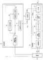
図18に、本実施形態の回路装置20、この回路装置20を含むジャイロセンサー510(広義には物理量検出装置)、このジャイロセンサー510を含む電子機器500の詳細な構成例を示す。
9. Detailed Configuration of Electronic Device, Gyro Sensor, and Circuit Device FIG. 18 shows a
なお回路装置20、電子機器500、ジャイロセンサー510は図18の構成に限定されず、その構成要素の一部を省略したり、他の構成要素を追加するなどの種々の変形実施が可能である。また本実施形態の電子機器500としては、デジタルカメラ、ビデオカメラ、スマートフォン、携帯電話機、カーナビゲーションシステム、ロボット、生体情報検出装置、ゲーム機、時計、健康器具、或いは携帯型情報端末等の種々の機器を想定できる。また以下では、物理量トランスデューサー(角速度センサー素子)が圧電型の振動片(振動ジャイロ)であり、センサーがジャイロセンサーである場合を例にとり説明するが、本発明はこれに限定されない。例えばシリコン基板などから形成された静電容量検出方式の振動ジャイロや、角速度情報と等価な物理量や角速度情報以外の物理量を検出する物理量トランスデューサー等にも本発明は適用可能である。
Note that the
電子機器500は、ジャイロセンサー510と処理部520を含む。またメモリー530、操作部540、表示部550を含むことができる。CPU、MPU等で実現される処理部520(外部の処理装置)は、ジャイロセンサー510等の制御や電子機器500の全体制御を行う。また処理部520は、ジャイロセンサー510により検出された角速度情報(広義には物理量)に基づいて処理を行う。例えば角速度情報に基づいて、手ぶれ補正、姿勢制御、GPS自律航法などのための処理を行う。メモリー530(ROM、RAM等)は、制御プログラムや各種データを記憶したり、ワーク領域やデータ格納領域として機能する。操作部540はユーザーが電子機器500を操作するためのものであり、表示部550は種々の情報をユーザーに表示する。
Electronic device 500 includes a
ジャイロセンサー510(物理量検出装置)は、振動片10と回路装置20を含む。振動片10(広義には物理量トランスデューサー、角速度センサー素子)は、水晶などの圧電材料の薄板から形成される圧電型振動片である。具体的には、振動片10は、Zカットの水晶基板により形成されたダブルT字型の振動片である。
The gyro sensor 510 (physical quantity detection device) includes the
回路装置20は、駆動回路30、FLL回路130、検出回路60、制御部140、レジスター部142、出力部144(インターフェース部)、不揮発性メモリー146、演算処理部150を含む。なお、これらの構成要素の一部を省略したり、他の構成要素を追加するなどの種々の変形実施が可能である。
The
FLL回路130は、駆動回路30からの信号に基づいてクロック信号を生成する。検出回路60は、A/D変換回路100、DSP部110を含み、これらA/D変換回路100、DSP部110と、演算処理部150、制御部140は、FLL回路130からのクロック信号又は、それを分周したクロック信号で動作する。
The
制御部140は、回路装置20の制御処理を行う。この制御部140は、ロジック回路(ゲートアレイ等)やプロセッサー等により実現できる。回路装置20での各種のスイッチ制御やモード設定等はこの制御部140により行われる。
The
駆動回路30は、駆動信号DQを出力して振動片10を駆動する。例えば振動片10からフィードバック信号DIを受け、これに対応する駆動信号DQを出力することで、振動片10を励振させる。検出回路60は、駆動信号DQにより駆動される振動片10から検出信号IQ1、IQ2(検出電流、電荷)を受け、検出信号IQ1、IQ2から、振動片10に印加された物理量に応じた所望信号(コリオリ力信号)を検出(抽出)する。
The
振動片10は、基部1と、連結腕2、3と、駆動腕4、5、6、7と、検出腕8、9を有する。矩形状の基部1に対して+Y軸方向、−Y軸方向に検出腕8、9が延出している。また基部1に対して−X軸方向、+X軸方向に連結腕2、3が延出している。そして連結腕2に対して+Y軸方向、−Y軸方向に駆動腕4、5が延出しており、連結腕3に対して+Y軸方向、−Y軸方向に駆動腕6、7が延出している。なおX軸、Y軸、Z軸は水晶の軸を示すものであり、各々、電気軸、機械軸、光学軸とも呼ばれる。
The
駆動回路30からの駆動信号DQは、駆動腕4、5の上面に設けられた駆動電極と、駆動腕6、7の側面に設けられた駆動電極に入力される。また駆動腕4、5の側面に設けられた駆動電極と、駆動腕6、7の上面に設けられた駆動電極からの信号が、フィードバック信号DIとして駆動回路30に入力される。また検出腕8、9の上面に設けられた検出電極からの信号が、検出信号IQ1、IQ2として検出回路60に入力される。なお検出腕8、9の側面に設けられたコモン電極は例えば接地される。
The drive signal DQ from the
駆動回路30により交流の駆動信号DQが印加されると、駆動腕4、5、6、7は、逆圧電効果により矢印Aに示すような屈曲振動(励振振動)を行う。即ち、駆動腕4、6の先端が互いに接近と離間を繰り返し、駆動腕5、7の先端も互いに接近と離間を繰り返す屈曲振動を行う。このとき駆動腕4、5と駆動腕6、7とが、基部1の重心位置を通るY軸に対して線対称の振動を行っているので、基部1、連結腕2、3、検出腕8、9はほとんど振動しない。
When an AC drive signal DQ is applied by the
この状態で、振動片10に対してZ軸を回転軸とした角速度が加わると(振動片10がZ軸回りで回転すると)、コリオリ力により駆動腕4、5、6、7は矢印Bに示すように振動する。即ち、矢印Aの方向とZ軸の方向とに直交する矢印Bの方向のコリオリ力が、駆動腕4、5、6、7に働くことで、矢印Bの方向の振動成分が発生する。この矢印Bの振動が連結腕2、3を介して基部1に伝わり、検出腕8、9が矢印Cの方向で屈曲振動を行う。この検出腕8、9の屈曲振動による圧電効果で発生した電荷信号が、検出信号IQ1、IQ2として検出回路60に入力される。ここで、駆動腕4、5、6、7の矢印Bの振動は、基部1の重心位置に対して周方向の振動であり、検出腕8、9の振動は、矢印Bとは周方向で反対向きの矢印Cの方向での振動である。検出信号IQ1、IQ2は、駆動信号DQに対して位相が90度だけずれた信号になる。
In this state, when an angular velocity with the Z axis as the rotation axis is applied to the vibrating piece 10 (when the vibrating
例えば、Z軸回りでの振動片10(ジャイロセンサー)の角速度をωとし、質量をmとし、振動速度をvとすると、コリオリ力はFc=2m・v・ωと表される。従って検出回路60が、コリオリ力に応じた信号である所望信号を検出することで、角速度ωを求めることができる。そして求められた角速度ωを用いることで、処理部520は、手振れ補正、姿勢制御、或いはGPS自律航法等のための種々の処理を行うことができる。
For example, when the angular velocity of the vibrating piece 10 (gyro sensor) around the Z axis is ω, the mass is m, and the vibration velocity is v, the Coriolis force is expressed as Fc = 2 m · v · ω. Therefore, the
なお図18では、振動片10がダブルT字型である場合の例を示しているが、本実施形態の振動片10はこのような構造に限定されない。例えば音叉型、H型等であってもよい。また振動片10の圧電材料は、水晶以外のセラミックスやシリコン等の材料であってもよい。
18 shows an example in which the
図19に回路装置の駆動回路30、検出回路60の詳細な構成例を示す。
FIG. 19 shows a detailed configuration example of the
駆動回路30は、振動片10からのフィードバック信号DIが入力される増幅回路32と、自動ゲイン制御を行うゲイン制御回路40と、駆動信号DQを振動片10に出力する駆動信号出力回路50を含む。また同期信号SYCを検出回路60に出力する同期信号出力回路52を含む。なお、駆動回路30の構成は図19に限定されず、これらの構成要素の一部を省略したり、他の構成要素を追加するなどの種々の変形実施が可能である。
The
増幅回路32(I/V変換回路)は、振動片10からのフィードバック信号DIを増幅する。例えば振動片10からの電流の信号DIを電圧の信号DVに変換して出力する。この増幅回路32は、演算増幅器、帰還抵抗素子、帰還キャパシターなどにより実現できる。
The amplification circuit 32 (I / V conversion circuit) amplifies the feedback signal DI from the
駆動信号出力回路50は、増幅回路32による増幅後の信号DVに基づいて、駆動信号DQを出力する。例えば駆動信号出力回路50が、矩形波(又は正弦波)の駆動信号を出力する場合には、駆動信号出力回路50はコンパレーター等により実現できる。
The drive
ゲイン制御回路40(AGC)は、駆動信号出力回路50に制御電圧DSを出力して、駆動信号DQの振幅を制御する。具体的には、ゲイン制御回路40は、信号DVを監視して、発振ループのゲインを制御する。例えば駆動回路30では、ジャイロセンサーの感度を一定に保つために、振動片10(駆動用振動片)に供給する駆動電圧の振幅を一定に保つ必要がある。このため、駆動振動系の発振ループ内に、ゲインを自動調整するためのゲイン制御回路40が設けられる。ゲイン制御回路40は、振動片10からのフィードバック信号DIの振幅(振動片の振動速度v)が一定になるように、ゲインを可変に自動調整する。このゲイン制御回路40は、増幅回路32の出力信号DVを全波整流する全波整流器や、全波整流器の出力信号の積分処理を行う積分器などにより実現できる。
The gain control circuit 40 (AGC) outputs a control voltage DS to the drive
同期信号出力回路52は、増幅回路32による増幅後の信号DVを受け、同期信号SYC(参照信号)を検出回路60に出力する。この同期信号出力回路52は、正弦波(交流)の信号DVの2値化処理を行って矩形波の同期信号SYCを生成するコンパレーターや、同期信号SYCの位相調整を行う位相調整回路(移相器)などにより実現できる。
The synchronization
また同期信号出力回路52は基準クロック信号CKFをFLL回路130に出力する。例えば同期信号出力回路52は、正弦波の信号DVの2値化処理を行うコンパレーターを含む。そして、例えばコンパレーターの出力信号を第1のバッファー回路でバッファリングした信号が同期信号SYCになり、コンパレーターの出力信号を第2のバッファー回路でバッファリングした信号が基準クロック信号CKFとなる。これにより基準クロック信号CKFと同期信号は例えば周波数が同じ信号になる。なお、同期信号SYCの生成用の第1のコンパレーターと、基準クロック信号CKFの生成用の第2のコンパレーターを設けてもよい。
The synchronization
検出回路60は、増幅回路61、同期検波回路81、フィルター部90、A/D変換回路100、DSP部110を含む。増幅回路61は、振動片10からの第1、第2の検出信号IQ1、IQ2を受けて、電荷−電圧変換や差動の信号増幅やゲイン調整などを行う。同期検波回路81は、駆動回路30からの同期信号SYCに基づいて同期検波を行う。フィルター部90(ローパスフィルター)は、A/D変換回路100の前置きフィルターとして機能する。またフィルター部90は、同期検波によっては除去しきれなかった不要信号を減衰する回路としても機能する。A/D変換回路100は、同期検波後の信号のA/D変換を行う。DSP部110はA/D変換回路100からのデジタル信号に対してデジタルフィルター処理やデジタル補正処理などのデジタル信号処理を行う。デジタル補正処理としては、例えばゼロ点補正処理や感度補正処理などがある。
The
なお、例えば振動片10からの電荷信号(電流信号)である検出信号IQ1、IQ2は、電圧信号である駆動信号DQに対して位相が90度遅れる。また増幅回路61のQ/V変換回路等において位相が90度遅れる。このため、増幅回路61の出力信号は駆動信号DQに対して位相が180度遅れる。従って、例えば駆動信号DQ(DV)と同相の同期信号SYCを用いて同期検波することで、駆動信号DQに対して位相が90度遅れた不要信号等を除去できるようになる。
For example, the detection signals IQ1 and IQ2 that are charge signals (current signals) from the vibrating
10.移動体、電子機器
図20(A)に本実施形態の回路装置20を含む移動体の例を示す。本実施形態の回路装置20は、例えば、車、飛行機、バイク、自転車、或いは船舶等の種々の移動体に組み込むことができる。移動体は、例えばエンジンやモーター等の駆動機構、ハンドルや舵等の操舵機構、各種の電子機器を備えて、地上や空や海上を移動する機器・装置である。図20(A)は移動体の具体例としての自動車206を概略的に示している。自動車206には、振動片10と回路装置20を有するジャイロセンサー510(センサー)が組み込まれている。ジャイロセンサー510は車体207の姿勢を検出することができる。ジャイロセンサー510の検出信号は車体姿勢制御装置208に供給される。車体姿勢制御装置208は例えば車体207の姿勢に応じてサスペンションの硬軟を制御したり個々の車輪209のブレーキを制御したりすることができる。その他、こういった姿勢制御は二足歩行ロボットや航空機、ヘリコプター等の各種の移動体において利用されることができる。姿勢制御の実現にあたってジャイロセンサー510は組み込まれることができる。
10. Mobile Object, Electronic Device FIG. 20A shows an example of a mobile object including the
図20(B)、図20(C)に示すように、本実施形態の回路装置はデジタルスチルカメラや生体情報検出装置(ウェアラブル健康機器。例えば脈拍計、歩数計、活動量計等)などの種々の電子機器に適用できる。例えばデジタルスチルカメラにおいてジャイロセンサーや加速度センサーを用いた手ぶれ補正等を行うことができる。また生体情報検出装置において、ジャイロセンサーや加速度センサーを用いて、ユーザーの体動を検出したり、運動状態を検出できる。また図20(D)に示すように、本実施形態の回路装置はロボットの可動部(アーム、関節)や本体部にも適用できる。ロボットは、移動体(走行・歩行ロボット)、電子機器(非走行・非歩行ロボット)のいずれも想定できる。走行・歩行ロボットの場合には、例えば自律走行に本実施形態の回路装置を利用できる。 As shown in FIGS. 20B and 20C, the circuit device of the present embodiment is a digital still camera, a biological information detection device (wearable health device, such as a pulse meter, a pedometer, an activity meter, etc.). It can be applied to various electronic devices. For example, camera shake correction using a gyro sensor or an acceleration sensor can be performed in a digital still camera. Further, in the biological information detection apparatus, it is possible to detect a user's body movement or an exercise state using a gyro sensor or an acceleration sensor. As shown in FIG. 20D, the circuit device of this embodiment can also be applied to a movable part (arm, joint) or main body part of a robot. As the robot, any of a moving body (running / walking robot) and an electronic device (non-running / non-walking robot) can be assumed. In the case of a traveling / walking robot, for example, the circuit device of this embodiment can be used for autonomous traveling.
なお、上記のように本実施形態について詳細に説明したが、本発明の新規事項および効果から実体的に逸脱しない多くの変形が可能であることは当業者には容易に理解できるであろう。従って、このような変形例はすべて本発明の範囲に含まれるものとする。例えば、明細書又は図面において、少なくとも一度、より広義または同義な異なる用語(物理量情報、角速度センサー素子、物理量検出装置等)と共に記載された用語(角速度情報、振動片、ジャイロセンサー等)は、明細書又は図面のいかなる箇所においても、その異なる用語に置き換えることができる。また、回路装置や物理量検出装置や電子機器や移動体の構成、振動片の構造等も、本実施形態で説明したものに限定されず、種々の変形実施が可能である。 Although the present embodiment has been described in detail as described above, it will be easily understood by those skilled in the art that many modifications can be made without departing from the novel matters and effects of the present invention. Accordingly, all such modifications are intended to be included in the scope of the present invention. For example, in the specification or drawings, terms (angular velocity information, vibration pieces, gyro sensors, etc.) described at least once together with different terms (physical quantity information, angular velocity sensor elements, physical quantity detection devices, etc.) in a broader sense or the same meaning The different terms can be used anywhere in the book or drawing. In addition, the configuration of the circuit device, the physical quantity detection device, the electronic device, the moving body, the structure of the vibrating piece, and the like are not limited to those described in the present embodiment, and various modifications can be made.
1 基部、2,3 連結腕、4〜7 駆動腕、8,9 検出腕、10 振動片、
12 物理量トランスデューサー、20 回路装置、30 駆動回路、
32 増幅回路、40 ゲイン制御回路、41 分周回路、42 差分器、
43 ループフィルター、44 加算器、45 周波数比較器、46 遅延回路、
48 発振器、50 駆動信号出力回路、52 同期信号出力回路、
60 検出回路、61 増幅回路、70 クロック信号生成回路、
72 D/A変換回路、74 電圧制御発振器、81 同期検波回路、
90 フィルター部、100 A/D変換回路、110 DSP部、
130 FLL回路、131 比較器、132 周波数比較器、
133 分周回路、134 発振器、135 カウンター、
136 ループフィルター、137 積分器、139 ゲイン処理部、
140 制御部、142 レジスター部、144 出力部、
146 不揮発性メモリー、150 演算処理部、155 乗算処理部、
156 積分処理部、160 浮動小数積分器、162 検出器、
164 固定小数積分器、166 固定小数変換部、168 レジスター、
169 レジスター、180 増幅回路、196 可変抵抗回路、
197 可変容量回路、206 自動車、207 車体、
208 車体姿勢制御装置、209 車輪、500 電子機器、
510 ジャイロセンサー、520 処理部、530 メモリー、
540 操作部、550 表示部、
CF 乗算係数、CKF 基準クロック信号、CTQ 比較対象値、
DQ 駆動信号、DR 分周比、DVQ 分周クロック信号、FR 駆動周波数、
FU1 ヒューズ素子、FV 発振周波数、OSQ クロック信号、
R1 抵抗素子、SC 基準値、TRM 発振周波数設定値、TQ 検出信号
1 base, 2, 3 connecting arm, 4-7 driving arm, 8, 9 detecting arm, 10 vibrating piece,
12 physical quantity transducers, 20 circuit devices, 30 drive circuits,
32 amplifier circuit, 40 gain control circuit, 41 frequency divider circuit, 42 differencer,
43 loop filter, 44 adder, 45 frequency comparator, 46 delay circuit,
48 oscillator, 50 drive signal output circuit, 52 synchronization signal output circuit,
60 detection circuit, 61 amplification circuit, 70 clock signal generation circuit,
72 D / A conversion circuit, 74 voltage controlled oscillator, 81 synchronous detection circuit,
90 filter section, 100 A / D conversion circuit, 110 DSP section,
130 FLL circuit, 131 comparator, 132 frequency comparator,
133 frequency divider, 134 oscillator, 135 counter,
136 loop filter, 137 integrator, 139 gain processing unit,
140 control unit, 142 register unit, 144 output unit,
146 Non-volatile memory, 150 arithmetic processing unit, 155 multiplication processing unit,
156 integration processing unit, 160 floating-point integrator, 162 detector,
164 fixed decimal number integrator, 166 fixed decimal number conversion unit, 168 register,
169 resistor, 180 amplifier circuit, 196 variable resistance circuit,
197 variable capacitance circuit, 206 automobile, 207 car body,
208 body posture control device, 209 wheels, 500 electronic devices,
510 gyro sensor, 520 processing unit, 530 memory,
540 operation unit, 550 display unit,
CF multiplication coefficient, CKF reference clock signal, CTQ comparison target value,
DQ drive signal, DR divider ratio, DVQ divided clock signal, FR drive frequency,
FU1 fuse element, FV oscillation frequency, OSQ clock signal,
R1 resistance element, SC reference value, TRM oscillation frequency setting value, TQ detection signal
Claims (15)
周波数比較器と発振器とを有し、前記駆動回路からの信号を基準クロック信号としてクロック信号を生成するFLL(Frequency Locked Loop)回路と、
前記物理量トランスデューサーからの検出信号の検出処理を行う検出回路と、
を含み、
前記検出回路は、
前記検出信号に基づく信号を同期検波する同期検波回路と、
前記クロック信号に基づく動作用信号により動作し、前記同期検波回路の出力信号に基づく信号をA/D変換するA/D変換回路と、
を有し、
前記駆動回路からの信号の周波数をFRとし、前記発振器が出力する前記クロック信号の周波数をFVとし、iを1以上の整数とし、jを1以上の整数とし、前記動作用信号の周波数をFV/iとする場合に、
j×FR≠FV/iであることを特徴とする回路装置。 A drive circuit for driving the physical quantity transducer;
An FLL (Frequency Locked Loop) circuit that has a frequency comparator and an oscillator, and generates a clock signal using a signal from the drive circuit as a reference clock signal;
A detection circuit for performing detection processing of the detection signal from the pre-Symbol physical quantity transducer,
Only including,
The detection circuit includes:
A synchronous detection circuit for synchronously detecting a signal based on the detection signal;
An A / D conversion circuit which operates by an operation signal based on the clock signal and performs A / D conversion on a signal based on the output signal of the synchronous detection circuit;
Have
The frequency of the signal from the driving circuit is FR, the frequency of the clock signal output from the oscillator is FV, i is an integer of 1 or more, j is an integer of 1 or more, and the frequency of the operation signal is FV. / I,
A circuit device, wherein j × FR ≠ FV / i .
前記周波数比較器は、
前記基準クロック信号を分周する分周回路と、
前記分周回路からの分周クロック信号と前記発振器からの前記クロック信号とに基づく比較対象値と、前記比較対象値の基準値との比較処理を行う比較器と、
を有することを特徴とする回路装置。 In claim 1,
The frequency comparator is
A frequency divider for dividing the reference clock signal;
A comparison target value based on the divided clock signal from the frequency divider circuit and the clock signal from the oscillator, and a comparator that performs a comparison process of a reference value of the comparison target value;
A circuit device comprising:
前記周波数比較器は、
前記分周クロック信号で規定される計測期間を、前記クロック信号によってカウントすることで計測されたカウント値を、前記比較対象値として出力するカウンターを有することを特徴とする回路装置。 In claim 2,
The frequency comparator is
A circuit device comprising: a counter that outputs a count value measured by counting a measurement period defined by the divided clock signal by the clock signal as the comparison target value.
前記基準値をSCとし、前記分周回路の分周比をDRとする場合に、
FV=(SC/DR)×FRであり、
j×FR≠FV/iとなるようにSC/DRが設定されることを特徴とする回路装置。 In claim 2 or 3,
The reference value is set to SC, the frequency division ratio of said divider circuit when shall be the DR,
FV = (SC / DR) × FR,
SC / DR is set such that j × FR ≠ FV / i .
SC/DRは小数であることを特徴とする回路装置。 In claim 4,
SC / DR is a decimal circuit device.
SCは小数であることを特徴とする回路装置。 In claim 4,
SC is a decimal circuit device.
前記発振器は、
前記周波数比較器の出力に基づく発振周波数設定値が設定され、前記発振周波数設定値に基づいて発振するCR発振回路を有することを特徴とする回路装置。 In any one of Claims 1 thru | or 6 ,
The oscillator is
A circuit device comprising a CR oscillation circuit in which an oscillation frequency setting value based on an output of the frequency comparator is set and oscillates based on the oscillation frequency setting value.
前記CR発振回路は、
可変容量回路及び可変抵抗回路の少なくとも一方を有し、
前記発振周波数設定値に応じて前記可変容量回路の容量値又は前記可変抵抗回路の抵抗値が設定されることで、前記CR発振回路の発振周波数が設定されることを特徴とする回
路装置。 In claim 7 ,
The CR oscillation circuit is
Having at least one of a variable capacitance circuit and a variable resistance circuit;
The circuit device, wherein the oscillation frequency of the CR oscillation circuit is set by setting a capacitance value of the variable capacitance circuit or a resistance value of the variable resistance circuit according to the oscillation frequency setting value.
前記CR発振回路は、
可変容量回路と可変抵抗回路とを有し、
前記可変抵抗回路は、
直列接続される複数の抵抗素子と、
前記複数の抵抗素子の各抵抗素子に対して各ヒューズ素子が並列に設けられる複数のヒューズ素子と、
を有し、
前記可変容量回路は、
前記発振周波数設定値に応じて容量値が設定される回路であることを特徴とする回路装置。 In claim 7 ,
The CR oscillation circuit is
A variable capacitance circuit and a variable resistance circuit;
The variable resistance circuit is:
A plurality of resistance elements connected in series;
A plurality of fuse elements in which each fuse element is provided in parallel with respect to each resistance element of the plurality of resistance elements;
Have
The variable capacitance circuit is:
A circuit device, wherein a capacitance value is set according to the oscillation frequency setting value.
前記周波数比較器と前記発振器の間に設けられるループフィルターを含むことを特徴とする回路装置。 In any one of Claims 1 thru | or 9 ,
A circuit device comprising a loop filter provided between the frequency comparator and the oscillator.
前記ループフィルターは、
前記周波数比較器の出力を積分する積分器と、
前記積分器の出力にゲイン処理を行うゲイン処理部と、
を有することを特徴とする回路装置。 In claim 10 ,
The loop filter is
An integrator for integrating the output of the frequency comparator;
A gain processing unit for performing gain processing on the output of the integrator;
A circuit device comprising:
前記検出回路は、
前記クロック信号に基づいて動作し、前記A/D変換回路の出力信号をデジタル処理するデジタル信号処理部を有することを特徴とする回路装置。 In any one of Claims 1 thru | or 11 ,
The detection circuit includes:
The operates based on the clock signal, the circuit device, characterized in that the output signal of the A / D converter circuit having a digital signal processor for digital processing.
前記クロック信号に基づいて動作し、前記駆動回路と前記検出回路を制御する制御部を含むことを特徴とする回路装置。 In any one of Claims 1 thru | or 12 ,
A circuit device comprising: a control unit that operates based on the clock signal and controls the drive circuit and the detection circuit.
Priority Applications (3)
| Application Number | Priority Date | Filing Date | Title |
|---|---|---|---|
| JP2015068078A JP6589333B2 (en) | 2015-03-30 | 2015-03-30 | Circuit device, electronic device and moving body |
| US15/082,319 US9590642B2 (en) | 2015-03-30 | 2016-03-28 | Circuit device, electronic apparatus, and moving object |
| CN201610188201.8A CN106027043B (en) | 2015-03-30 | 2016-03-29 | Circuit device, electronic apparatus, and moving object |
Applications Claiming Priority (1)
| Application Number | Priority Date | Filing Date | Title |
|---|---|---|---|
| JP2015068078A JP6589333B2 (en) | 2015-03-30 | 2015-03-30 | Circuit device, electronic device and moving body |
Publications (3)
| Publication Number | Publication Date |
|---|---|
| JP2016189514A JP2016189514A (en) | 2016-11-04 |
| JP2016189514A5 JP2016189514A5 (en) | 2018-05-17 |
| JP6589333B2 true JP6589333B2 (en) | 2019-10-16 |
Family
ID=57016354
Family Applications (1)
| Application Number | Title | Priority Date | Filing Date |
|---|---|---|---|
| JP2015068078A Active JP6589333B2 (en) | 2015-03-30 | 2015-03-30 | Circuit device, electronic device and moving body |
Country Status (3)
| Country | Link |
|---|---|
| US (1) | US9590642B2 (en) |
| JP (1) | JP6589333B2 (en) |
| CN (1) | CN106027043B (en) |
Families Citing this family (13)
| Publication number | Priority date | Publication date | Assignee | Title |
|---|---|---|---|---|
| JP6455174B2 (en) * | 2015-01-22 | 2019-01-23 | セイコーエプソン株式会社 | CIRCUIT DEVICE, ELECTRONIC DEVICE, MOBILE BODY AND PHYSICAL QUANTITY DETECTION DEVICE MANUFACTURING METHOD |
| JP6586735B2 (en) | 2015-02-20 | 2019-10-09 | セイコーエプソン株式会社 | Circuit device, physical quantity detection device, electronic device, and moving object |
| JP6492739B2 (en) * | 2015-02-20 | 2019-04-03 | セイコーエプソン株式会社 | Circuit device, physical quantity detection device, electronic device, and moving object |
| JP6862900B2 (en) * | 2017-02-22 | 2021-04-21 | セイコーエプソン株式会社 | Circuit devices, physical quantity measuring devices, electronic devices and mobile objects |
| JP6478207B2 (en) * | 2017-03-10 | 2019-03-06 | ヒロテック株式会社 | IFFT clock adjusting device, IFFT clock adjusting method, and digital television broadcasting device |
| JP2018163037A (en) * | 2017-03-27 | 2018-10-18 | セイコーエプソン株式会社 | Circuit device, physical quantity detection device, electronic equipment, and moving body |
| CN107544617A (en) * | 2017-07-27 | 2018-01-05 | 宏祐图像科技(上海)有限公司 | A kind of local clock production method and circuit for SERDES chips |
| IT201700103058A1 (en) * | 2017-09-14 | 2019-03-14 | St Microelectronics Srl | CIRCUIT AND DRIVING METHOD FOR A MEMS GYROSCOPE AND ITS MEMS GYROSCOPE |
| JP7040253B2 (en) * | 2018-04-20 | 2022-03-23 | セイコーエプソン株式会社 | Physical quantity sensor module, inclinometer, inertial measurement unit, structure monitoring device, and moving object |
| US11177797B2 (en) | 2019-01-02 | 2021-11-16 | Beijing Boe Technology Development Co., Ltd. | Measuring device and measuring method |
| CN111464182A (en) * | 2020-04-29 | 2020-07-28 | 四川玖越机器人科技有限公司 | Inspection robot |
| US11418203B2 (en) * | 2020-09-16 | 2022-08-16 | Mediatek Singapore Pte. Ltd. | Frequency locked loops and related circuits and methods |
| KR102468771B1 (en) * | 2021-03-17 | 2022-11-18 | 숭실대학교 산학협력단 | Frequency adaptive lock-in amplifier based harmonic elimination method for single-phase grid-connected inverter, recording medium and device for performing the method |
Family Cites Families (14)
| Publication number | Priority date | Publication date | Assignee | Title |
|---|---|---|---|---|
| JP2752613B2 (en) * | 1986-07-08 | 1998-05-18 | 日本電気株式会社 | Clock regeneration circuit |
| JP4098298B2 (en) * | 2004-11-16 | 2008-06-11 | ローム株式会社 | CR oscillation circuit and electronic device |
| US7711078B2 (en) * | 2007-06-01 | 2010-05-04 | Smsc Holdings Sarl | Frequency synchronization |
| JP2009162645A (en) * | 2008-01-08 | 2009-07-23 | Panasonic Corp | Inertial velocity sensor signal processing circuit and inertial velocity sensor device having the same |
| JP4794596B2 (en) * | 2008-04-04 | 2011-10-19 | パナソニック株式会社 | Physical quantity detection circuit, physical quantity sensor device |
| CN101272142B (en) * | 2008-05-20 | 2011-05-18 | 曹秀娟 | Frequency synthesizer |
| JP5369525B2 (en) | 2008-07-28 | 2013-12-18 | パナソニック株式会社 | PLL circuit and angular velocity sensor using the same |
| JP2010185714A (en) * | 2009-02-10 | 2010-08-26 | Panasonic Corp | System and device for physical quantity sensor |
| US8179174B2 (en) * | 2010-06-15 | 2012-05-15 | Mstar Semiconductor, Inc. | Fast phase locking system for automatically calibrated fractional-N PLL |
| JP5601292B2 (en) | 2011-03-31 | 2014-10-08 | 株式会社デンソー | Digital phase synchronization circuit and physical quantity detection sensor |
| CN103168419A (en) * | 2011-05-09 | 2013-06-19 | 松下电器产业株式会社 | Resistance-capacitance oscillation circuit |
| JP6185741B2 (en) * | 2013-04-18 | 2017-08-23 | ルネサスエレクトロニクス株式会社 | Frequency-locked loop circuit and semiconductor integrated circuit |
| JP2016171493A (en) * | 2015-03-13 | 2016-09-23 | セイコーエプソン株式会社 | Circuit device, electronic apparatus and moving body |
| JP6315531B1 (en) * | 2017-11-09 | 2018-04-25 | 株式会社片山抜型製作所 | Female die for punching machine and punching machine |
-
2015
- 2015-03-30 JP JP2015068078A patent/JP6589333B2/en active Active
-
2016
- 2016-03-28 US US15/082,319 patent/US9590642B2/en active Active
- 2016-03-29 CN CN201610188201.8A patent/CN106027043B/en active Active
Also Published As
| Publication number | Publication date |
|---|---|
| CN106027043B (en) | 2021-02-05 |
| JP2016189514A (en) | 2016-11-04 |
| CN106027043A (en) | 2016-10-12 |
| US9590642B2 (en) | 2017-03-07 |
| US20160294397A1 (en) | 2016-10-06 |
Similar Documents
| Publication | Publication Date | Title |
|---|---|---|
| JP6589333B2 (en) | Circuit device, electronic device and moving body | |
| CN102686976B (en) | Angular velocity sensor | |
| CN107306132B (en) | Circuit device, oscillator, electronic apparatus, and moving object | |
| JP6720672B2 (en) | Circuit devices, oscillators, electronic devices and mobile units | |
| JP6728652B2 (en) | Circuit device, oscillator, electronic device, moving body, and oscillator manufacturing method | |
| JP6623616B2 (en) | Circuit devices, physical quantity sensors, oscillators, electronic equipment, and moving objects | |
| US9869986B2 (en) | Detection device, sensor, electronic apparatus, and moving object | |
| US20180278259A1 (en) | Circuit device, physical quantity measurement device, electronic device, and vehicle | |
| JP6720687B2 (en) | Circuit devices, oscillators, electronic devices and mobile units | |
| CN107026643B (en) | Circuit device, oscillator, electronic apparatus, and moving object | |
| CN111669125B (en) | Oscillator, electronic apparatus, and moving object | |
| US10254115B2 (en) | Circuit device, physical quantity detection device, electronic apparatus, and moving object | |
| CN111669124B (en) | Oscillator, electronic apparatus, and moving object | |
| US20210285769A1 (en) | Physical Quantity Detection Circuit, Physical Quantity Sensor, And Operating Method For Physical Quantity Detection Circuit | |
| JP6561702B2 (en) | Physical quantity detection system, electronic device and moving object | |
| US10175044B2 (en) | Circuit device, physical quantity detection device, electronic apparatus, and moving object | |
| JP6572585B2 (en) | CIRCUIT DEVICE, PHYSICAL QUANTITY DETECTION DEVICE, ELECTRONIC DEVICE, MOBILE BODY, CIRCUIT DEVICE MANUFACTURING METHOD | |
| JP2017085536A (en) | Circuit device, oscillator, electronic equipment and mobile body | |
| JP2019174422A (en) | Circuit arrangement, and physical quantity measuring device, oscillator, electronic apparatus, and movable body using the same | |
| JP2010271172A (en) | Physical quantity detection device |
Legal Events
| Date | Code | Title | Description |
|---|---|---|---|
| A521 | Request for written amendment filed |
Free format text: JAPANESE INTERMEDIATE CODE: A523 Effective date: 20180326 |
|
| A621 | Written request for application examination |
Free format text: JAPANESE INTERMEDIATE CODE: A621 Effective date: 20180326 |
|
| A977 | Report on retrieval |
Free format text: JAPANESE INTERMEDIATE CODE: A971007 Effective date: 20190124 |
|
| A131 | Notification of reasons for refusal |
Free format text: JAPANESE INTERMEDIATE CODE: A131 Effective date: 20190219 |
|
| A521 | Request for written amendment filed |
Free format text: JAPANESE INTERMEDIATE CODE: A523 Effective date: 20190410 |
|
| TRDD | Decision of grant or rejection written | ||
| A01 | Written decision to grant a patent or to grant a registration (utility model) |
Free format text: JAPANESE INTERMEDIATE CODE: A01 Effective date: 20190820 |
|
| A61 | First payment of annual fees (during grant procedure) |
Free format text: JAPANESE INTERMEDIATE CODE: A61 Effective date: 20190902 |
|
| R150 | Certificate of patent or registration of utility model |
Ref document number: 6589333 Country of ref document: JP Free format text: JAPANESE INTERMEDIATE CODE: R150 |