CN1043831C - Apparatus for storage of chips, apparatus for orientation of position in which chips are taken out and system for supplying chips - Google Patents
Apparatus for storage of chips, apparatus for orientation of position in which chips are taken out and system for supplying chips Download PDFInfo
- Publication number
- CN1043831C CN1043831C CN92111839A CN92111839A CN1043831C CN 1043831 C CN1043831 C CN 1043831C CN 92111839 A CN92111839 A CN 92111839A CN 92111839 A CN92111839 A CN 92111839A CN 1043831 C CN1043831 C CN 1043831C
- Authority
- CN
- China
- Prior art keywords
- chip
- leading screw
- vertical panel
- cartridges
- travelling carriage
- Prior art date
- Legal status (The legal status is an assumption and is not a legal conclusion. Google has not performed a legal analysis and makes no representation as to the accuracy of the status listed.)
- Expired - Fee Related
Links
Images


Classifications
-
- H—ELECTRICITY
- H01—ELECTRIC ELEMENTS
- H01L—SEMICONDUCTOR DEVICES NOT COVERED BY CLASS H10
- H01L23/00—Details of semiconductor or other solid state devices
-
- H—ELECTRICITY
- H05—ELECTRIC TECHNIQUES NOT OTHERWISE PROVIDED FOR
- H05K—PRINTED CIRCUITS; CASINGS OR CONSTRUCTIONAL DETAILS OF ELECTRIC APPARATUS; MANUFACTURE OF ASSEMBLAGES OF ELECTRICAL COMPONENTS
- H05K13/00—Apparatus or processes specially adapted for manufacturing or adjusting assemblages of electric components
- H05K13/0061—Tools for holding the circuit boards during processing; handling transport of printed circuit boards
-
- H—ELECTRICITY
- H01—ELECTRIC ELEMENTS
- H01L—SEMICONDUCTOR DEVICES NOT COVERED BY CLASS H10
- H01L21/00—Processes or apparatus adapted for the manufacture or treatment of semiconductor or solid state devices or of parts thereof
- H01L21/67—Apparatus specially adapted for handling semiconductor or electric solid state devices during manufacture or treatment thereof; Apparatus specially adapted for handling wafers during manufacture or treatment of semiconductor or electric solid state devices or components ; Apparatus not specifically provided for elsewhere
- H01L21/677—Apparatus specially adapted for handling semiconductor or electric solid state devices during manufacture or treatment thereof; Apparatus specially adapted for handling wafers during manufacture or treatment of semiconductor or electric solid state devices or components ; Apparatus not specifically provided for elsewhere for conveying, e.g. between different workstations
- H01L21/67703—Apparatus specially adapted for handling semiconductor or electric solid state devices during manufacture or treatment thereof; Apparatus specially adapted for handling wafers during manufacture or treatment of semiconductor or electric solid state devices or components ; Apparatus not specifically provided for elsewhere for conveying, e.g. between different workstations between different workstations
- H01L21/67721—Apparatus specially adapted for handling semiconductor or electric solid state devices during manufacture or treatment thereof; Apparatus specially adapted for handling wafers during manufacture or treatment of semiconductor or electric solid state devices or components ; Apparatus not specifically provided for elsewhere for conveying, e.g. between different workstations between different workstations the substrates to be conveyed not being semiconductor wafers or large planar substrates, e.g. chips, lead frames
-
- H—ELECTRICITY
- H01—ELECTRIC ELEMENTS
- H01L—SEMICONDUCTOR DEVICES NOT COVERED BY CLASS H10
- H01L21/00—Processes or apparatus adapted for the manufacture or treatment of semiconductor or solid state devices or of parts thereof
- H01L21/67—Apparatus specially adapted for handling semiconductor or electric solid state devices during manufacture or treatment thereof; Apparatus specially adapted for handling wafers during manufacture or treatment of semiconductor or electric solid state devices or components ; Apparatus not specifically provided for elsewhere
- H01L21/677—Apparatus specially adapted for handling semiconductor or electric solid state devices during manufacture or treatment thereof; Apparatus specially adapted for handling wafers during manufacture or treatment of semiconductor or electric solid state devices or components ; Apparatus not specifically provided for elsewhere for conveying, e.g. between different workstations
- H01L21/67703—Apparatus specially adapted for handling semiconductor or electric solid state devices during manufacture or treatment thereof; Apparatus specially adapted for handling wafers during manufacture or treatment of semiconductor or electric solid state devices or components ; Apparatus not specifically provided for elsewhere for conveying, e.g. between different workstations between different workstations
- H01L21/67736—Loading to or unloading from a conveyor
-
- H—ELECTRICITY
- H01—ELECTRIC ELEMENTS
- H01L—SEMICONDUCTOR DEVICES NOT COVERED BY CLASS H10
- H01L21/00—Processes or apparatus adapted for the manufacture or treatment of semiconductor or solid state devices or of parts thereof
- H01L21/67—Apparatus specially adapted for handling semiconductor or electric solid state devices during manufacture or treatment thereof; Apparatus specially adapted for handling wafers during manufacture or treatment of semiconductor or electric solid state devices or components ; Apparatus not specifically provided for elsewhere
- H01L21/677—Apparatus specially adapted for handling semiconductor or electric solid state devices during manufacture or treatment thereof; Apparatus specially adapted for handling wafers during manufacture or treatment of semiconductor or electric solid state devices or components ; Apparatus not specifically provided for elsewhere for conveying, e.g. between different workstations
- H01L21/67763—Apparatus specially adapted for handling semiconductor or electric solid state devices during manufacture or treatment thereof; Apparatus specially adapted for handling wafers during manufacture or treatment of semiconductor or electric solid state devices or components ; Apparatus not specifically provided for elsewhere for conveying, e.g. between different workstations the wafers being stored in a carrier, involving loading and unloading
- H01L21/67769—Storage means
-
- Y—GENERAL TAGGING OF NEW TECHNOLOGICAL DEVELOPMENTS; GENERAL TAGGING OF CROSS-SECTIONAL TECHNOLOGIES SPANNING OVER SEVERAL SECTIONS OF THE IPC; TECHNICAL SUBJECTS COVERED BY FORMER USPC CROSS-REFERENCE ART COLLECTIONS [XRACs] AND DIGESTS
- Y10—TECHNICAL SUBJECTS COVERED BY FORMER USPC
- Y10S—TECHNICAL SUBJECTS COVERED BY FORMER USPC CROSS-REFERENCE ART COLLECTIONS [XRACs] AND DIGESTS
- Y10S414/00—Material or article handling
- Y10S414/10—Associated with forming or dispersing groups of intersupporting articles, e.g. stacking patterns
- Y10S414/102—Associated with forming or dispersing groups of intersupporting articles, e.g. stacking patterns including support for group
- Y10S414/103—Vertically shiftable
- Y10S414/105—Shifted by article responsive means
-
- Y—GENERAL TAGGING OF NEW TECHNOLOGICAL DEVELOPMENTS; GENERAL TAGGING OF CROSS-SECTIONAL TECHNOLOGIES SPANNING OVER SEVERAL SECTIONS OF THE IPC; TECHNICAL SUBJECTS COVERED BY FORMER USPC CROSS-REFERENCE ART COLLECTIONS [XRACs] AND DIGESTS
- Y10—TECHNICAL SUBJECTS COVERED BY FORMER USPC
- Y10S—TECHNICAL SUBJECTS COVERED BY FORMER USPC CROSS-REFERENCE ART COLLECTIONS [XRACs] AND DIGESTS
- Y10S414/00—Material or article handling
- Y10S414/10—Associated with forming or dispersing groups of intersupporting articles, e.g. stacking patterns
- Y10S414/114—Adjust to handle articles or groups of different sizes
Abstract
Cs with leadframes can be efficiently transferred, stocked and positioned without the need for preparing jigs for each kind of IC. A cassette 4 accommodating a stack of ICs is inserted into a cassette space 35 and held in the center thereof. A moving table 9 is driven to move by a servomotor 21. A lifting member 67 of an IC lifting mechanism 60 raises the ICs in the cassette 4 from the bottom by an amount corresponding to the thickness of one IC at a time. A pulling-over device 70, which is disposed above the cassette space 35, centers the IC in both the lateral and longitudinal directions to thereby effect positioning.
Description
The present invention relates to the feed system of integrated circuit (IC) chip (hereinafter to be referred as chip).More particularly, the chip feedway among the present invention comprises chip storage apparatus and chip extracting position positioner, and the chip storage apparatus is the storage apparatus that a kind of bunchiness chip of confession band lead frame is used; Chip extracting position positioner be a kind of after from this storage apparatus, taking out chip the device that circuit or machining center position position that transports to Any shape size chip.
In the prior art; integrated circuit (IC) chip is through after the various manufacturing processes; chip for using lead frame roughly also has following manufacturing procedure: with chip adhere on the lead frame, chip and lead frame inter-rack wiring, for protect chip with coverings such as plastics be laminating material mould, the punch process of on outer cover, marking, lead frame being carried out bending or cut-out etc.
Above-mentioned these processing technologys are carried out in each operation successively, to behind the chip location, implement required processing in the processing unit (plant) that is provided with in each operation.The chip of different size, its lead frame and packaging size, shape also have nothing in common with each other.In order to carry out above-mentioned each manufacturing procedure continuously, the chip in must will processing in the process of transporting or in processing unit (plant) is positioned on the desired location.Therefore, can only use and the size of this chip, each processing unit (plant) that specification conforms to.
In order to make processing unit (plant) be common to the chip of all size, to have adopted chip cartridges, the receptacle that holds chip cartridges that stacked chips is housed, transport with anchor clamps, assembling with anchor clamps etc.But because chip kind difference, the specification of the shape of its lead frame and packing, size etc. is different.Therefore, need be according to the quantity of chip kind, prepare the chip cartridges that is applicable to every kind of chip in advance, transport with anchor clamps, assembling with anchor clamps etc.In addition,, also to change above-mentioned each anchor clamps, increase the processing time of operation according to the chip of every kind of lot number if change at manufacture process chips lot number.
The present invention is based on above-mentioned prior art and makes, and its purpose is to provide a kind of chip feed system of using for the chip of band lead frame, so that in the manufacture process of the chip of band lead frame, reduces the time of positioning action.
Another object of the present invention provides a kind of need not the transformation and has the chip feed system that processing unit (plant) just can use easily now.
To achieve these goals, the invention provides chip feed system with following structure, this system by the travelling carriage that on the 1st framework, moves, be used to the moving table driving equipment that drives above-mentioned travelling carriage, make it to be positioned at desired location on the framework, and be positioned in and be used to adorn on the above-mentioned travelling carriage if constitute in the chip cartridges of sheet stacked chips, it is characterized in that also comprising:
Be used to clamp and grip a plurality of the 1st vertical panels and the 2nd vertical panel of said chip box,
Be used to make interconnective the 1st jockey of above-mentioned polylith the 1st vertical panel,
Be used to make interconnective the 2nd jockey of above-mentioned a plurality of the 2nd vertical panel,
Be used to make above-mentioned the 1st jockey and the 2nd jockey to make the relative movement of drive unit that relatively moves,
Be used for the described chip that is stacked in described chip cartridges is ejected the chip elevating mechanism that comes from the foot of described chip cartridges, and
Be used to make and describedly from chip cartridges, eject the superiors chip location of coming and make it occupy the center and dispose the centralising device of the upper position of described chip cartridges.
According to another kind of design of the present invention, chip with following structure feed system is provided, this system by the travelling carriage that moves on the 1st framework, be used to drive described travelling carriage and make it to be positioned at desired location on the described framework the travelling carriage drive unit, be arranged on the described travelling carriage and the chip cartridges that several pieces integrated circuit (IC) chip are stacked together constitutes, it is characterized in that also comprising:
Polylith the 1st vertical panel and the 2nd vertical panel are used to clamp and grip the said chip box;
The 1st jockey is used to make above-mentioned polylith the 1st vertical panel to interconnect;
The 2nd jockey is used to make above-mentioned polylith the 2nd vertical panel to interconnect;
Relative movement of drive unit is used to make above-mentioned the 1st vertical panel and the 2nd vertical panel to relatively move;
The chip cartridges fixture is used for described chip cartridges is positioned the center of the depth direction of the box space that described chip cartridges marked off by described the 1st vertical panel and the 2nd vertical panel;
The chip elevating mechanism is used for the foot of the described chip that is stacked in described chip cartridges from described chip cartridges ejected;
Centralising device is used to make describedly to eject the superiors chip location of coming and make it occupy the center and dispose the upper position of described chip cartridges from chip cartridges.
Below, with reference to the description of drawings embodiments of the invention.
Fig. 1 is the casing stereogram of seeing from the storage apparatus front.
Fig. 2 is the chip plane graph of expression band lead frame.
Fig. 3 is the chip cartridges stereogram.
Fig. 4 is the right side view of storage apparatus biopsy cavity marker devices.
Fig. 5 is the 2nd vertical panel partial sectional view that the V direction is seen from Fig. 1.
Fig. 6 is the plane graph of Fig. 5.
Fig. 7 is the left surface figure of Fig. 5.
Fig. 8 is the front plan view that centralising device top is dissectd.
Fig. 9 is the plane graph of Fig. 8.
Figure 10 is the right side view of Fig. 8.
Figure 11 is the profile along XI among Fig. 8-the XI line dissects.
Fig. 1 is the casing stereogram of chip storage apparatus 1 summary of expression band lead frame.As shown in Figure 2, in the present embodiment, the chip 2 on the lead frame 3 sends from last operation with 5 states that are connected.Chip 2 installs to (see figure 3) on the storage apparatus 1 with the stacked state of multilayer by manual or automated manner in chip cartridges 4.The side of chip cartridges 4, the end and top are opened wide, and as described later, chip 2 is ejected by the bottom of Lift Part 67 (seeing Fig. 1,4) from chip cartridges 4, therefore can take out chip 2 from the top block-by-block of chip cartridges 4.
The shape of chip 2, size have nothing in common with each other because of its kind is different, so will prepare the chip cartridges 4 of various different sizes in advance.Chip cartridges 4 is clamped in the storage apparatus 1, uses mechanism described later, can be by piece take out chip 2 from chip cartridges 4 tops.
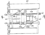
Below introduce storage apparatus 1.Fig. 4 is the right hand view with storage apparatus 1 anterior partly cut-away.On the framework 6 of storage apparatus 1, guide post 7 and the plane spigot surface 8 done by straight rod iron are being set, this spigot surface 8 has parallel spigot surface up and down.Above guide post 7 and plane spigot surface 8, travelling carriage 9 is being set.Below the place ahead of travelling carriage 9, rolling bearing 10 is being set, this rolling bearing 10 moves on guide post 7.Below the rear of travelling carriage 9, fixing the upper end of the supporting member of making by vertical panel 11 with methods such as welding.
In the lower end of supporting member 11,2 rolling running rollers 12,12 are being set, this rolling running roller 12,12 clips the parallel spigot surface about in the of two of planar guide face 8 and moves.Therefore, travelling carriage 9 is set on guide post 7, the planar guide face 8 with moving freely.In the front lower of travelling carriage 9, be provided with the vertical walls whole with 9 one-tenth of travelling carriages----front side wall 13.
Below travelling carriage 9, fixing ball nut (figure does not show).In this ball nut, screwing in screw rod---feed screw 16 (see figure 1)s.The two ends of feed screw 16 by two bearings 17,17, can be rotated to support on the framework 6.At an end of feed screw 16, fixing timing belt pulley 18, sheathed synchronous belt 19 on timing belt pulley 18, and this synchronous belt 19 is overlapping timing belt pulley 20.This timing belt pulley 20 links to each other with AC servomotor 21 and by its driving.Therefore, according to the control device instruction of (figure does not show), travelling carriage 9 is driven by AC servomotor 21, moves on guide post 7 and plane spigot surface 8, and is positioned on the required optional position.
On travelling carriage 9, mutually opposed and leave the compartment of terrain 3 the 1st vertical panels 22 and 3 the 2nd vertical panels 23 are set.Space between the 1st vertical panel 22 and the 2nd vertical panel 23 is 3 box spaces 35 that hold chip cartridges 4.3 the 1st vertical panels 22 interconnect by the 1st top connecting plate 24 and the 1st bottom connecting plate 25, and therefore, 3 the 1st vertical panels 22 are to move linkedly mutually.
On the top of the 1st bottom connecting plate 25, fixing the 1st tooth bar 26.Similarly, 3 the 2nd vertical panels 23 also interconnect by the 2nd connecting plate 27.Therefore, 3 the 2nd vertical panels also are to move linkedly mutually.In the bottom of the 2nd connecting plate 27, fixing the 2nd tooth bar 28.Pinion 29 is meshing with the 1st tooth bar 26 and the 2nd tooth bar 28 simultaneously.
On pinion 29, knob 30 (see figure 4)s coaxial with axle 31 are being set.The front end of axle 31, by bearing 32, rotation is bearing on the front side wall 13 of travelling carriage 9 freely.Therefore, when turning knob 30, pinion 29 is rotation just, makes the 1st tooth bar 26 and the 2nd tooth bar 28 mobile phase same distance in the opposite direction simultaneously.Because moving of the 1st tooth bar 26 and the 2nd tooth bar 28, make 3 the 1st vertical panels and the 2nd vertical panel abreast simultaneously mutually near or deviate from mutually.
Between the 1st vertical panel 22 and the 2nd vertical panel 23, form box space 35.In illustrated example, 3 box space 35 (see figure 1)s are arranged.Chip cartridges 4 is clamped by two pawls 49,46 that be oppositely arranged, that fixed bin body is used in box space 35.This chip cartridges 4 is clamped in the depth (promptly) of box space 35 and the center position of the standard width of a room in an old-style house (being Width) both direction.As previously mentioned, the width of chip cartridges 4 is different and different because of the shape of chip 2 with length.
In order to be fit to the chip cartridges 4 of virtually any size, width of box space 35 (standard width of a room in an old-style house) and length (depth) can be regulated.Use the interlinked mechanism that constitutes by above-mentioned the 1st tooth bar the 26, the 2nd tooth bar 28 and pinion 29 to carry out the Width location of box space 35.After having set interlinked mechanism, the width adjusting of box space 35 is become the width consistent with chip cartridges 4 and fixes it with lock-screw 14.Lock-screw 14 is used to make top connecting plate 24 and the 2nd connecting plate 27 to be fixedly clamped mutually.The location of box space 35 depth directions is held mechanism 40 with following box body mounting board and is carried out.
The part sectioned view of Fig. 5 V direction, expression the 2nd vertical panel 23 from Fig. 1.Fig. 6 is the profile that dissects along V1-V1 line among Fig. 5.Fig. 7 is the left surface figure of Fig. 5.Locating up and down in the 1st vertical panel 22 is being provided with 2 parallel screw rods---leading screw 41a, 41b.On leading screw 41a, 41b, be the boundary with the centre of its length direction, carve respectively and establishing right-hand thread and left-hand thread.End at leading screw 41a is connecting knob 42, rotates this knob 42 with hand, and leading screw 41a is rotated.
At the other end of leading screw 41a, 41b, fixing timing belt pulley 43a, 43b.Between these 2 timing belt pulley 43a, 43b, the sheathed synchronous belt 44 of seeing.On the right-hand thread of leading screw 41a, 41b, left-hand thread, screwing in 4 nut 45a, 45b, 45c and 45d respectively.At 2 nut 45a, 45c, fixing the L shaped the 1st and holding pawl 46.On other 2 nut 45b, 45d, fixing the 2nd and holding pawl 47.
The 2nd to hold pawl 47 can be center rotation (see figure 6) with axle 48, and under the pushing of spring, always press to the direction of box space 35.On the 2nd top that holds pawl 47, being provided with axle 50 is the push plate 49 that the center rotates freely.Push plate 49 pushes the 2nd towards the direction of the 2nd vertical panel 23 and holds pawl 47 under the effect of spring.
Therefore, when antagonistic spring was tried hard to recommend moving push plate 49, push plate 49 was that swing at the center with axle 50 just.Push plate 49 pushing the 2nd holds pawl 47, the 2, and to hold pawl 47 be that rotate at the center with axle 48, thereby chip cartridges 4 can push the 2nd and block 47 and insert (direction of arrow).Chip cartridges 4 is stuck in the 1st and holds pawl 46 and the 2nd and hold between the pawl 47, so in case insert and just can not take out.Chip cartridges 4 from box space 35 positive insertions, is utilized this function exactly.As a result, chip cartridges 4 just is positioned on the direction centre position, front and back (depth) of box space 35.
Fig. 7 is the left surface figure of Fig. 5.Rear between the 1st vertical panel 22 and the 2nd vertical panel 23, the 3rd vertical panel 50 is arranged on the travelling carriage 9.On the 3rd vertical panel 50, be provided with abreast 4 levels to guide post 51a, 51b, 51c and 51d.On guide post 51a, 51b, 51c and 51d, inserting mobile member 52a, 52b, 52c and the 52d that can move freely by bearing respectively.
Be separately fixed on the 1st vertical panel 22 with the end of Screw with moving-member 52a, 52d, therefore, the 1st vertical panel 22 moves with moving-member 52a, 52d are whole.Be respectively fixed on the 2nd vertical panel 23 with the end of Screw with moving- member 52b, 52c, therefore, the 2nd vertical panel 23 moves with moving- member 52b, 52c are whole.
2 rotatable connecting rod 55a, 55b are installed in respectively on axle 54a, the 54b of the 3rd vertical panel 50.There is the U-shaped groove at the two ends of connecting rod 55a, 55b, and pin 53a, 53b, 53c and 53d insert in this groove.Therefore,, drive the 1st vertical panel 22 and the 2nd vertical panel 23 as connecting rod 55a, when 55b moves, make they abreast mutually near or deviate from mutually.
Expressed chip elevating mechanism 60 among Fig. 1 and Fig. 4.Be stacked in the chip 2 in the chip cartridges 4, be transported the device block-by-block from top and take out and be transferred to subsequent processing.At this moment, just need chip 2 up be pushed up, so that take out chip from the foot of chip cartridges 4.Chip elevating mechanism 60 is exactly to be used for device that stacked chip 2 is up pushed away from the bottom.On the framework 6 of 1 one jiaos of storage apparatus, in vertical direction rotating screw rod 61 is set by bearing 62,62.In the lower end of screw rod 61, fixing timing belt pulley 63.Sheathed the synchronous belt 64 that drives by servo motor (figure does not show) on this timing belt pulley 63.On screw rod 61, screw in ball nut 65.
On ball nut 65, become integrally fixing arm 66.At the front end of arm 66, become integrally be provided with Lift Part 67.Lift Part 67 is from the bottom of chip cartridges 4, is unit with the thickness of chip piece, above chip 2 is pushed up.
Fig. 8 is a centralising device broken section front elevation.Fig. 9 is the plane graph of Fig. 8.Figure 10 is the left surface figure of Fig. 8.Figure 11 is the profile that dissects along the X1-X1 line along among Fig. 8.On the top of rectangular frame 71,2 rotatable leading screw 72a, 72b (see figure 9) are be arrangeding in parallel.
On leading screw 72a, 72b, be that the boundary is scribing right-hand thread and left-hand thread respectively with the centre.End at screw mandrel 72b is connecting knob 73; The other end is being fixed timing belt pulley 74.On timing belt pulley 74, sheathed synchronous belt 75.
Therefore, when turning knob 73, leading screw 72b is rotation just, and this rotation is delivered to leading screw 72a by timing belt pulley 74, synchronous belt 75 and timing belt pulley 76, and leading screw 72a is also rotated.Because the rotation of leading screw 72a, 72b makes nut 77a, 77b, 77c and 77d move, and drive centering plate 78a and 78b, make them make to clap mutual connection closely or the motion that deviates from mutually with respect to the center line of centralising device 70.Like this, chip 2 just always remains on the center of centralising device 70.
Above-described is the mechanism that makes the Width centering of a string IC chip 2.In the bottom of centralising device 70, length (depth) the direction location and the centering body of same principle therewith are being set.Figure 11 is the plane graph of cutting open along the X1-X1 line of Fig. 8.In the bottom of framework 71,2 rotatable leading screw 82a, 82b are be arrangeding in parallel.
On leading screw 82a, 82b,, carve respectively and putting right-hand thread and left-hand thread to be the boundary in the middle of it.At the end of leading screw 82b, fixing knob 83, the other end is being fixed timing belt pulley 84.On timing belt pulley 84, sheathed synchronous belt 85.
Therefore, when turning knob 83, screw mandrel 82b is rotation just, and with similarly aforementioned, this rotation finally makes centering plate 88a, 88b mutual approaching or deviate from mutually with respect to center line.Like this, chip 2 to length (depth) direction is located and centering.As previously discussed, to the rectangle lead frame 3 of various different lengths, need only turning knob 73,83, just can set its center in length and breadth.In addition, the center of machined object often remains unchanged.Be that width, length direction all are positioned at the center, be transplanted on subsequent processing after, the processing of subsequent processing is just more convenient.
Introduce the course of action of apparatus of the present invention below.
The chip 2 that last working procedure processing ends, be contained in the unidimensional chip cartridges 4 of chip 2 in brought.This chip cartridges 4 is inserted from box space 35 fronts of storage apparatus 1.For the chip cartridges 4 that is applicable to virtually any size, the width of box space 35 and length are adjustable, the location of the Width of box space 35 (standard width of a room in an old-style house), and the interlinked mechanism of being made up of above-mentioned the 1st tooth bar the 26, the 2nd tooth bar 28 and pinion carries out.
Behind the width setup, the width of box space 35 is fixed with lock-screw 14.Lock-screw 14 is used to make top connecting plate 24 and the 2nd connecting plate 27 fastening mutually.The location of box space 35 depth directions is undertaken by above-mentioned box body catch mechanism 40.Insert in box body 4 the place ahead while pushing pawl 49 from box space 35.The pawl 46 and the 2nd that fixedly holds that the front end of box body 4 is held in the 1st vertical panel 22 holds between the pawl 47.
Then, start AC servomotor 21, drive timing belt pulley 20, synchronous belt 19 and timing belt pulley 18, make feed screw 16 rotations.The rotation of this feed screw 16 makes travelling carriage 9 move on guide post 7 and plane spigot surface 8.When the good box space 35 of travelling carriage 9 adjusted was positioned on the Lift Part 67 of elevating mechanism 60, travelling carriage stopped to move.
Then, screw rod 61 is driven rotation by servo motor (figure does not show), and Lift Part 67 has only raised the thickness of a slice chip 2 upward.Because moving up of this Lift Part 67 in the feasible chip 2 that is configured in box space 35 tops, has only chip piece 2 to enter in the centralising device 70.At this moment, centering is located by centering plate 78a, 78b in the position of Width, and centering is located by centering plate 88a, 88b in the length direction center simultaneously.After reserve the position, chip 2 is transplanted on subsequent processing from the top of centralising device 70 by conveyer (figure do not show).
When the chip 2 in the box space 35 used up, lift component 67 was got back to original position.Start AC servomotor 21 once more, travelling carriage is moved, next box space 35 is delivered to the bottom of centralising device 70, repeat above-mentioned action.
As mentioned above, the present invention can be expeditiously positions, centering, deposits and transport size, variform chip, therefore unnecessaryly prepares to transport anchor clamps according to every batch of chip, and assembling fixture etc. have remarkable result.
Claims (6)
1. chip feed system, by the travelling carriage (9) that go up to move at the 1st framework (6), be used to drive described travelling carriage 9 and make it to be positioned at described framework (6) go up the travelling carriage drive unit (16-21) of desired location, be arranged on that described travelling carriage (9) is gone up and the chip cartridges (4) that several pieces integrated circuit (IC) chip (2) stack together is constituted, it is characterized in that also comprising:
Polylith the 1st vertical panel (22) and the 2nd vertical panel (23) are used to clamp and grip the said chip box;
The 1st jockey (24,25) is used to make above-mentioned polylith the 1st vertical panel (22) to interconnect;
The 2nd jockey (27) is used to make above-mentioned polylith the 2nd vertical panel (23) to interconnect;
Relative movement of drive unit (26,27,29 ...), be used to make above-mentioned the 1st vertical panel (22) and the 2nd vertical panel (23) to relatively move;
Chip elevating mechanism (60) is used for the foot of the described chip (2) that is stacked in described chip cartridges (4) from described chip cartridges (4) ejected; And
Centralising device (70) is used to make the described the superiors' chip (2) that comes that ejects from chip cartridges (4) locate and make it occupy the center and dispose the upper position of described chip cartridges (4).
2. chip feed system, by the travelling carriage (9) that go up to move at the 1st framework (6), be used to drive described travelling carriage 9 and make it to be positioned at described framework (6) go up the travelling carriage drive unit (16-21) of desired location, be arranged on that described travelling carriage (9) is gone up and the chip cartridges (4) that several pieces integrated circuit (IC) chip (2) stack together is constituted, it is characterized in that also comprising:
Polylith the 1st vertical panel (22) and the 2nd vertical panel (23) are used to clamp and grip the said chip box;
The 1st jockey (24,25) is used to make above-mentioned polylith the 1st vertical panel (22) to interconnect;
The 2nd jockey (27) is used to make above-mentioned polylith the 2nd vertical panel (23) to interconnect;
Relative movement of drive unit (26,27,29 ...), be used to make above-mentioned the 1st vertical panel (22) and the 2nd vertical panel (23) to relatively move;
Chip cartridges fixture (40) is used for described chip cartridges (4) is positioned the center of the depth direction of the box space (35) that described chip cartridges (4) marked off by described the 1st vertical panel (22) and the 2nd vertical panel (23);
Chip elevating mechanism (60) is used for the foot of the described chip (2) that is stacked in described chip cartridges (4) from described chip cartridges (4) ejected;
Centralising device (70) is used to make the described the superiors' chip (2) that comes that ejects from chip cartridges (4) locate and make it occupy the center and dispose the upper position of described chip cartridges (4).
3. chip feed system as claimed in claim 1 or 2 is characterized in that:
Described centralising device (70) comprising:
The 2nd framework (71),
At least two the 1st leading screws that be arranged in parallel with described the 2nd framework (71) (82a, 82b);
Be formed on described each the 1st leading screw (82a, 82b) last, the mutual pair of opposite bolt of screw thread;
Be screwed at least 4 the 1st nuts (87a-87d) on the described bolt;
At least be connected between two described the 1st nuts, the 1st centering plate of configuration parallel to each other (88a, 88b);
Be fixed on described the 1st leading screw (82a, 82b) the 1st belt pulley (84,86) on is so that described first leading screw (82a, 82b) rotates;
Be used to be connected the 1st belt (85) between described two the 1st belt pulleys (84,86), and
(82a one of 82b) goes up and drives described the 1st leading screw (82a, each the 1st drive unit (83) 82b) to be arranged on the 1st leading screw.
4. chip feed system as claimed in claim 3 is characterized in that also comprising:
Be arranged in parallel with described the 2nd thick stick frame (71) and with described the 1st leading screw (82a, 82b) at least two of arranged perpendicular the 2nd leading screws (72a, 72b);
Be formed on each the 2nd leading screw (72a, 72b) last, the mutual pair of opposite bolt of screw thread;
Be screwed at least 4 the 2nd nuts (77a-77d) on the described bolt;
Couple together between two described the 2nd nuts of major general (77a-77d), parallel to each other be configured in the 2nd centering plate (78a, 78b);
Be fixed on each the 2nd belt pulley (74,76) on each described the 2nd leading screw (72a, 72b), so as to rotate described each the 2nd leading screw (72a, 72b);
Be used to be connected the 2nd belt (75) between each described the 2nd belt pulley (74,76), and
(72a one of 72b) goes up and rotates described the 2nd leading screw (72a, the 2nd drive unit (73) 72b) to be arranged on described the 2nd leading screw.
5. as the chip feed system of claim 1 or 2, it is characterized in that:
Described relative movement of drive unit (26,27,29 ...) constitute by gear (26,28) and pinion (29).
6. chip feed system as claimed in claim 2 is characterized in that:
Described chip cartridges fixture (40) comprising:
At least two leading screws that be arranged in parallel with described the 1st vertical panel (22) (41a, 41b);
Be formed on described each leading screw (41a, 41b) last, the mutual pair of opposite bolt of screw thread;
At least 4 nuts (45a-45d) that are screwed on the described bolt;
(41a is connected between at least 2 described nuts (45a-45d) between 41b), configuration parallel to each other, is used for the 1st gripper jaw (46) and the 2nd gripper jaw (47) from the described chip cartridges of sandwich (4) at described each leading screw;
Be fixed on each belt pulley (43a, 43b) on the described leading screw (41a, 41b), so that described each leading screw (41a, 41b) rotates;
Be connected the belt (44) between described each belt pulley (43a, 43b), and
Be arranged on the drive unit (42) that one of described leading screw (41a, 416) is gone up, rotated described leading screw (41a, 41b).
Applications Claiming Priority (3)
| Application Number | Priority Date | Filing Date | Title |
|---|---|---|---|
| JP34818091A JP3147451B2 (en) | 1991-12-04 | 1991-12-04 | IC stocker, IC take-out positioning device and IC supply system |
| JP348180/91 | 1991-12-04 | ||
| JP348180/90 | 1991-12-04 |
Publications (2)
| Publication Number | Publication Date |
|---|---|
| CN1078342A CN1078342A (en) | 1993-11-10 |
| CN1043831C true CN1043831C (en) | 1999-06-23 |
Family
ID=18395284
Family Applications (1)
| Application Number | Title | Priority Date | Filing Date |
|---|---|---|---|
| CN92111839A Expired - Fee Related CN1043831C (en) | 1991-12-04 | 1992-12-04 | Apparatus for storage of chips, apparatus for orientation of position in which chips are taken out and system for supplying chips |
Country Status (9)
| Country | Link |
|---|---|
| US (1) | US5645393A (en) |
| EP (1) | EP0570589B1 (en) |
| JP (1) | JP3147451B2 (en) |
| KR (1) | KR100253168B1 (en) |
| CN (1) | CN1043831C (en) |
| AT (1) | ATE157064T1 (en) |
| DE (1) | DE69221717T2 (en) |
| TW (1) | TW303981U (en) |
| WO (1) | WO1993011061A1 (en) |
Cited By (1)
| Publication number | Priority date | Publication date | Assignee | Title |
|---|---|---|---|---|
| CN103043440A (en) * | 2011-10-11 | 2013-04-17 | 上海华族实业有限公司 | Ceramic positive temperature coefficient (PTC) ceramic wafer automatic feeding system and feeding method thereof |
Families Citing this family (14)
| Publication number | Priority date | Publication date | Assignee | Title |
|---|---|---|---|---|
| JP3147451B2 (en) * | 1991-12-04 | 2001-03-19 | 株式会社石井工作研究所 | IC stocker, IC take-out positioning device and IC supply system |
| KR970053345A (en) * | 1995-12-30 | 1997-07-31 | 김광호 | Carrier Transfer Device |
| TW353649B (en) * | 1996-12-03 | 1999-03-01 | Ishii Tool & Engineering Corp | IC leadframe processing system |
| JPH11156566A (en) * | 1997-11-28 | 1999-06-15 | Mitsubishi Electric Corp | Laser marking device and controlling method therefor |
| US6135291A (en) * | 1998-01-16 | 2000-10-24 | Micron Electronics, Inc. | Vertical magazine method for integrated circuit device dispensing, receiving, storing, testing or binning |
| US6719518B2 (en) * | 2001-10-15 | 2004-04-13 | Anadigics, Inc. | Portable tube holder apparatus |
| US20040168287A1 (en) * | 2001-12-19 | 2004-09-02 | Chun-Tsai Yang | Pressing apparatus for a semiconductor device |
| CN100465076C (en) * | 2004-02-09 | 2009-03-04 | 王广生 | Intelligent storing device |
| WO2011058644A1 (en) * | 2009-11-13 | 2011-05-19 | 株式会社データンク | Flash memory automatic feeder |
| WO2011058643A1 (en) * | 2009-11-13 | 2011-05-19 | 株式会社データンク | Magazine for flash memories |
| CN102070020B (en) * | 2010-11-01 | 2013-04-10 | 沙洲职业工学院 | Automatic feeding device in solar battery slice detector |
| CN106185138B (en) * | 2015-07-20 | 2018-06-01 | 亚洲硅业(青海)有限公司 | A kind of closed silicon core automatic access device |
| CN108861521A (en) * | 2018-07-19 | 2018-11-23 | 广州明森科技股份有限公司 | A kind of movable type card collection device |
| CN113471114B (en) * | 2021-09-03 | 2021-11-12 | 四川明泰电子科技有限公司 | Semiconductor integrated circuit package forming apparatus |
Family Cites Families (17)
| Publication number | Priority date | Publication date | Assignee | Title |
|---|---|---|---|---|
| US3410421A (en) * | 1966-04-01 | 1968-11-12 | Alvin F. Groll | Sheet stacker |
| JPS60242140A (en) * | 1984-05-15 | 1985-12-02 | Mita Ind Co Ltd | Paper feed device |
| JPS62169424A (en) * | 1986-01-22 | 1987-07-25 | Hitachi Tokyo Electron Co Ltd | Assembly machine |
| JPS62183629A (en) * | 1986-02-07 | 1987-08-12 | Fujitsu Ltd | Line switching device |
| JPH0442270Y2 (en) * | 1986-05-14 | 1992-10-06 | ||
| JPH06561B2 (en) * | 1987-06-22 | 1994-01-05 | 日立電子エンジニアリング株式会社 | Multiple magazine loading device |
| JP2717658B2 (en) * | 1987-11-27 | 1998-02-18 | 東芝メカトロニクス 株式会社 | Magazine exchange device |
| JPH01212449A (en) * | 1988-02-20 | 1989-08-25 | Daido Steel Co Ltd | Hybrid ic substrate feeder |
| KR970011656B1 (en) * | 1988-02-25 | 1997-07-12 | 도오교오 에레구토론 사가미 가부시끼가이샤 | Water transfer method |
| JPH0646645B2 (en) * | 1988-08-25 | 1994-06-15 | 株式会社東芝 | Lead frame carrier |
| NL8901522A (en) * | 1989-06-16 | 1991-01-16 | Hoogovens Groep Bv | DEVICE FOR HANDLING A CARRIER. |
| JPH03211145A (en) * | 1990-01-09 | 1991-09-13 | Mitsubishi Electric Corp | Lead frame conveying method and device |
| JP2751517B2 (en) * | 1990-01-24 | 1998-05-18 | 松下電器産業株式会社 | Lead frame stocker device |
| JPH03232628A (en) * | 1990-02-05 | 1991-10-16 | Fujitsu Ltd | Magazine conveying device |
| JP2740032B2 (en) * | 1990-02-23 | 1998-04-15 | 株式会社東芝 | Lead frame transfer device |
| JP2819182B2 (en) * | 1990-05-07 | 1998-10-30 | 株式会社新川 | Transfer device |
| JP3147451B2 (en) * | 1991-12-04 | 2001-03-19 | 株式会社石井工作研究所 | IC stocker, IC take-out positioning device and IC supply system |
-
1991
- 1991-12-04 JP JP34818091A patent/JP3147451B2/en not_active Expired - Fee Related
-
1992
- 1992-11-30 KR KR1019930701811A patent/KR100253168B1/en not_active IP Right Cessation
- 1992-11-30 EP EP92924035A patent/EP0570589B1/en not_active Expired - Lifetime
- 1992-11-30 WO PCT/JP1992/001571 patent/WO1993011061A1/en active IP Right Grant
- 1992-11-30 US US08/094,039 patent/US5645393A/en not_active Expired - Fee Related
- 1992-11-30 DE DE69221717T patent/DE69221717T2/en not_active Expired - Fee Related
- 1992-11-30 AT AT92924035T patent/ATE157064T1/en not_active IP Right Cessation
- 1992-12-04 CN CN92111839A patent/CN1043831C/en not_active Expired - Fee Related
-
1993
- 1993-02-11 TW TW084212457U patent/TW303981U/en unknown
Cited By (1)
| Publication number | Priority date | Publication date | Assignee | Title |
|---|---|---|---|---|
| CN103043440A (en) * | 2011-10-11 | 2013-04-17 | 上海华族实业有限公司 | Ceramic positive temperature coefficient (PTC) ceramic wafer automatic feeding system and feeding method thereof |
Also Published As
| Publication number | Publication date |
|---|---|
| EP0570589A4 (en) | 1994-03-09 |
| TW303981U (en) | 1997-04-21 |
| US5645393A (en) | 1997-07-08 |
| ATE157064T1 (en) | 1997-09-15 |
| WO1993011061A1 (en) | 1993-06-10 |
| EP0570589A1 (en) | 1993-11-24 |
| EP0570589B1 (en) | 1997-08-20 |
| JPH05155408A (en) | 1993-06-22 |
| CN1078342A (en) | 1993-11-10 |
| JP3147451B2 (en) | 2001-03-19 |
| DE69221717D1 (en) | 1997-09-25 |
| KR930703700A (en) | 1993-11-30 |
| KR100253168B1 (en) | 2000-04-15 |
| DE69221717T2 (en) | 1998-01-15 |
Similar Documents
| Publication | Publication Date | Title |
|---|---|---|
| CN1043831C (en) | Apparatus for storage of chips, apparatus for orientation of position in which chips are taken out and system for supplying chips | |
| US6293002B1 (en) | Heat exchanger assembling apparatus | |
| JPH0441029A (en) | Method and device for selecting and integrating many numbers of small products | |
| CN113695886A (en) | Charger assembly production equipment, assembly method and intelligent industrial control equipment | |
| CN112917148B (en) | Control assembly assembling equipment of environment-friendly air purifier | |
| JP3109801B2 (en) | IC lead frame processing system | |
| CN210876317U (en) | Full-automatic laser sorting equipment | |
| CN218696441U (en) | Steering mechanism behind cutting of photovoltaic cold-formed steel for support | |
| CN110625375A (en) | Upper and lower shell assembling machine | |
| CN218004238U (en) | Industrial robot operating platform | |
| CN110581199A (en) | Solar cell string typesetting equipment and method | |
| KR19980063635A (en) | IC lead frame processing system | |
| CN217626319U (en) | Automatic inserting piece equipment | |
| CN212268752U (en) | PCB processing and conveying machine | |
| JPH05728A (en) | Tray changer device and tray supply method | |
| CN220240387U (en) | Thermos cup production mechanism of integrated multistation | |
| CN215046868U (en) | A sheet material automatic feeding device for 5G production usefulness | |
| CN219362443U (en) | Positioning and adjusting mechanism for exchanging multiple-row material tool | |
| CN116111789B (en) | Stepping motor assembly production line | |
| CN215796882U (en) | Memory bank plug-in unit feeding device | |
| CN218704202U (en) | Full-automatic batch nozzle packing machine | |
| CN216266910U (en) | Intelligent engraving and milling machine | |
| CN220617442U (en) | Directional propulsion device for bearing roller production | |
| CN214070523U (en) | Automatic electronic components's of cartridge equipment | |
| CN212216696U (en) | Ten-axis numerical control bending equipment |
Legal Events
| Date | Code | Title | Description |
|---|---|---|---|
| C06 | Publication | ||
| PB01 | Publication | ||
| C53 | Correction of patent of invention or patent application | ||
| CB02 | Change of applicant information |
Applicant after: Ishi Work Institute Co., Ltd. Applicant before: Ishii Mitoshi |
|
| COR | Change of bibliographic data |
Free format text: CORRECT: APPLICANT; FROM: KENTOSHI ISHI TO: CO., LTD., ISHII WORKING INST. |
|
| C14 | Grant of patent or utility model | ||
| GR01 | Patent grant | ||
| C19 | Lapse of patent right due to non-payment of the annual fee | ||
| CF01 | Termination of patent right due to non-payment of annual fee |