CN1031088C - Process for forming functional deposited film - Google Patents
Process for forming functional deposited film Download PDFInfo
- Publication number
- CN1031088C CN1031088C CN89100622.2A CN89100622A CN1031088C CN 1031088 C CN1031088 C CN 1031088C CN 89100622 A CN89100622 A CN 89100622A CN 1031088 C CN1031088 C CN 1031088C
- Authority
- CN
- China
- Prior art keywords
- film
- deposited film
- gas release
- gas
- compound
- Prior art date
- Legal status (The legal status is an assumption and is not a legal conclusion. Google has not performed a legal analysis and makes no representation as to the accuracy of the status listed.)
- Expired - Fee Related
Links
Images


Classifications
-
- C—CHEMISTRY; METALLURGY
- C23—COATING METALLIC MATERIAL; COATING MATERIAL WITH METALLIC MATERIAL; CHEMICAL SURFACE TREATMENT; DIFFUSION TREATMENT OF METALLIC MATERIAL; COATING BY VACUUM EVAPORATION, BY SPUTTERING, BY ION IMPLANTATION OR BY CHEMICAL VAPOUR DEPOSITION, IN GENERAL; INHIBITING CORROSION OF METALLIC MATERIAL OR INCRUSTATION IN GENERAL
- C23C—COATING METALLIC MATERIAL; COATING MATERIAL WITH METALLIC MATERIAL; SURFACE TREATMENT OF METALLIC MATERIAL BY DIFFUSION INTO THE SURFACE, BY CHEMICAL CONVERSION OR SUBSTITUTION; COATING BY VACUUM EVAPORATION, BY SPUTTERING, BY ION IMPLANTATION OR BY CHEMICAL VAPOUR DEPOSITION, IN GENERAL
- C23C16/00—Chemical coating by decomposition of gaseous compounds, without leaving reaction products of surface material in the coating, i.e. chemical vapour deposition [CVD] processes
- C23C16/44—Chemical coating by decomposition of gaseous compounds, without leaving reaction products of surface material in the coating, i.e. chemical vapour deposition [CVD] processes characterised by the method of coating
- C23C16/50—Chemical coating by decomposition of gaseous compounds, without leaving reaction products of surface material in the coating, i.e. chemical vapour deposition [CVD] processes characterised by the method of coating using electric discharges
- C23C16/511—Chemical coating by decomposition of gaseous compounds, without leaving reaction products of surface material in the coating, i.e. chemical vapour deposition [CVD] processes characterised by the method of coating using electric discharges using microwave discharges
-
- C—CHEMISTRY; METALLURGY
- C23—COATING METALLIC MATERIAL; COATING MATERIAL WITH METALLIC MATERIAL; CHEMICAL SURFACE TREATMENT; DIFFUSION TREATMENT OF METALLIC MATERIAL; COATING BY VACUUM EVAPORATION, BY SPUTTERING, BY ION IMPLANTATION OR BY CHEMICAL VAPOUR DEPOSITION, IN GENERAL; INHIBITING CORROSION OF METALLIC MATERIAL OR INCRUSTATION IN GENERAL
- C23C—COATING METALLIC MATERIAL; COATING MATERIAL WITH METALLIC MATERIAL; SURFACE TREATMENT OF METALLIC MATERIAL BY DIFFUSION INTO THE SURFACE, BY CHEMICAL CONVERSION OR SUBSTITUTION; COATING BY VACUUM EVAPORATION, BY SPUTTERING, BY ION IMPLANTATION OR BY CHEMICAL VAPOUR DEPOSITION, IN GENERAL
- C23C16/00—Chemical coating by decomposition of gaseous compounds, without leaving reaction products of surface material in the coating, i.e. chemical vapour deposition [CVD] processes
- C23C16/44—Chemical coating by decomposition of gaseous compounds, without leaving reaction products of surface material in the coating, i.e. chemical vapour deposition [CVD] processes characterised by the method of coating
- C23C16/448—Chemical coating by decomposition of gaseous compounds, without leaving reaction products of surface material in the coating, i.e. chemical vapour deposition [CVD] processes characterised by the method of coating characterised by the method used for generating reactive gas streams, e.g. by evaporation or sublimation of precursor materials
- C23C16/452—Chemical coating by decomposition of gaseous compounds, without leaving reaction products of surface material in the coating, i.e. chemical vapour deposition [CVD] processes characterised by the method of coating characterised by the method used for generating reactive gas streams, e.g. by evaporation or sublimation of precursor materials by activating reactive gas streams before their introduction into the reaction chamber, e.g. by ionisation or addition of reactive species
-
- C—CHEMISTRY; METALLURGY
- C23—COATING METALLIC MATERIAL; COATING MATERIAL WITH METALLIC MATERIAL; CHEMICAL SURFACE TREATMENT; DIFFUSION TREATMENT OF METALLIC MATERIAL; COATING BY VACUUM EVAPORATION, BY SPUTTERING, BY ION IMPLANTATION OR BY CHEMICAL VAPOUR DEPOSITION, IN GENERAL; INHIBITING CORROSION OF METALLIC MATERIAL OR INCRUSTATION IN GENERAL
- C23C—COATING METALLIC MATERIAL; COATING MATERIAL WITH METALLIC MATERIAL; SURFACE TREATMENT OF METALLIC MATERIAL BY DIFFUSION INTO THE SURFACE, BY CHEMICAL CONVERSION OR SUBSTITUTION; COATING BY VACUUM EVAPORATION, BY SPUTTERING, BY ION IMPLANTATION OR BY CHEMICAL VAPOUR DEPOSITION, IN GENERAL
- C23C16/00—Chemical coating by decomposition of gaseous compounds, without leaving reaction products of surface material in the coating, i.e. chemical vapour deposition [CVD] processes
- C23C16/44—Chemical coating by decomposition of gaseous compounds, without leaving reaction products of surface material in the coating, i.e. chemical vapour deposition [CVD] processes characterised by the method of coating
- C23C16/52—Controlling or regulating the coating process
Abstract
A functional deposited film as a thin semiconductor film constituted, by introducing, into a film forming space, a compound as the film-forming raw material and, if required, a compound containing an element capable of controlling valence electrons for the deposited film as the constituent element each in a gaseous state, or in a state where at least one of the compounds is activated, while forming hydrogen atoms in an excited state causing chemical reaction with the compounds in the gaseous state or in the activated state in an activation space, thereby forming a deposited film on a substrate, wherein the hydrogen atoms in the excited state are formed from a hydrogen gas or a gas mixture composed of a hydrogen gas and a rare gas by means of a microwave plasma generated in a plasma generation chamber disposed in a cavity resonator integrated with two impedance matching circuits in a microwave circuit and the excited state of the hydrogen atoms is controlled.
Description
The present invention relates to form the functional deposited film that contains the main composed atom of the 4th family atom conduct, or contain silicon atom and the 4th family atom as the improvement of the functional deposited film of main composed atom method, this functional deposited film can be made the photocon of semiconductor device and be used in electronics to videotape technology specially, resemble the incoming line transducer, imaging device, the light-sensitive device of Photvoltaic device or similar device.
More particularly, the present invention relates on substrate, to form effectively functional deposited film improvement method, this is to be caused the hydrogen atom that excites that is in excitation state by microwave plasma by the mist with hydrogen or hydrogen and inert gas composition, and the hydrogen atom of described excitation state is contacted in film forming room with the film forming unstrpped gas of film forming unstrpped gas or activation separately, thereby generation chemical reaction, control simultaneously that the excitation state of hydrogen atom carries out, microwave plasma is to place the plasma generation chamber of the resonant cavity that combines with two widely different roads of impedance matching to produce in the widely different road of a microwave.
To functional deposited film, the particularly formation of semiconductor deposition film, existed consider with desired electricity, physical property with and use the film build method that adapts.
For example, tried out plasma chemical vapor deposition (CVD) method, active sputtering method, ion plating method, the optical cvd method, thermoinducible CVD method, MO CVD method, MBE methods etc. have in them severally to be used in the industrial production because of the semiconductor device that is suitable for forming requirement.
But, even in the plasma CVD method that has been widely adopted, consider and make required semiconductor device, the electricity of the deposited film that produces and physical property neither be satisfied with very much, sometimes plasma stability and formation deposited film is repeated bad, and it can cause the remarkable reduction of productivity ratio in addition.
For overcoming these problems, for example in the open 60-41047 of Japan Patent, proposed a method that increases the film deposition rate, thereby used hydrogenation base CVD method (HR-CVD method) to improve the productivity ratio of high-quality the 4th family's semiconductor film of deposition formation significantly.
Further, as using about 2.45 capital conspicuous (10 effectively
9Hz) microwave forms the means of high-density plasma, in open 55-141729 of Japan Patent for example and 57-133636, proposed the widely different method of revolving resonance (ECR) condition of electronics is set up in electromagnet design on the resonant cavity, and also reported method with high-density plasma formation classes of semiconductors film in academic conference etc.
By the way, in above-mentioned HR-CVD method, though the hydrogen atom of activated state (hydrogen base) has important effect to the character and the uniformity of the deposited film that control forms, but a large amount of excitation state of also controlling hydrogen atom equably during for the formation deposited film, and under excitation state control, forming the reaction of deposited film time control inhibition and generation, thereby the character of the deposited film that control selectively and stably forms is research fully, has still stayed several problems that will solve.
On the other hand, in the microwave plasma CVD device that uses ECR, several problems are arranged also.That is: for setting up the ECR condition, the pressure in plasma generation chamber must remain below about 10
-3Torr, like this pressure that forms deposited film there has been restriction: under the pressure of this level, increased gas molecule mean free path (being approximately 1 meter), film forming unstrpped gas is diffused near the microwave introduction window mouth thus, be reduced there and react, deposited film is sticked on microwave introduction window mouth or the resonant cavity inwall, thereby make discharge instability; On-chip film is stain by the fragment of adhesive film and scattering thing.Further also pointed out several problems, that is, the plasma that produces in plasma generation chamber is diffused into film forming room along the magnetic field of dispersing of electromagnet.Substrate places the higher plasma of density in film forming room.Therefore, the deposited film of formation is easy to by charged particle damage or the like, and this has just limited the character of improving the film that will form.In the step of the layer by layer deposition film of making the semiconductor device process, because the damage that charged particle causes, the border characteristic usually is lowered or the like, and this just is difficult to improve the characteristic of semiconductor device.
Main purpose of the present invention is the variety of issue that overcomes in the art methods of above-mentioned formation deposited film, and provide a required functional deposited film that comprises the 4th family atom of periodic table as main composed atom, or comprise silicon atom and described the 4th family atom required functional deposited film as main composed atom, it is big that it has an area, satisfied uniformity, advantages such as good stability and repeatability are effective to making high-quality semiconductor device.
The present inventor has carried out conscientious research for realizing purpose of the present invention to overcoming the of the prior art above-mentioned variety of issue that forms deposited film, thereby recognize the plasma generation chamber of resonant cavity that can be by placing two impedance matching widely different road combinations of the widely different Lu Zhongyu of microwave, and carry out microwave plasma discharge with hydrogen or the admixture of gas formed by hydrogen and a kind of inert gas, stably and effectively provide the hydrogen atom that is in the selectable excitation state with good repeatability.
The present invention is further research and realize that it comprises following two embodiment on the basis of above-mentioned cognition.
Relate to a kind of formation according to the first embodiment of the present invention (below be called " first invention ") and comprise the atom that belongs to periodic table the 4th family method as the functional deposited film of main composed atom, it introduces a kind of compound of periodic table tetrels that comprises as the film forming raw material to the film formation space at the substrate place that forms deposited film, and, if desired, introduce a kind of element that can control the deposited film valence electron as constituent, each all is in gaseous state, or be at least a compound and forming the state that activates in advance in the activation space that the space separates with film, form the excitation state hydrogen atom simultaneously, with be in gaseous state or be different from least a compound generation chemical reaction that is in activated state in the activation space of film formation space one, and they are introduced film formation space, on substrate, form deposited film at film formation space, the microwave plasma that produces of the plasma generation chamber of the resonant cavity that combines with two widely different roads of impedance matching by placing the widely different road of a microwave wherein, form the hydrogen atom of excitation state from the mist of hydrogen or hydrogen and a kind of inert gas, and the excitation state of hydrogen atom is controlled.
Relate to a formation method that comprises the mat woven of fine bamboo strips four family's atoms and silicon atom as the functional deposited film of main composed atom according to second embodiment of the present invention (below be called " second invention "), its feature description is as follows:
Second invention relates to a kind of method that forms deposited film, it forms the space to the film at the substrate place that forms deposited film thereon and introduces and a kind ofly contain the compound (1) of silicon and compound (2) that the general formula (I) below a kind of usefulness is represented makes the pleurodiaphragmatic in terspace material, and, if necessary, introduce and a kind ofly contain a kind of compound (3) of the element of deposited film valence electron of controlling as constituent, each all is in gaseous state or is at least a state that has activated in advance in the compound (1) (2) (3) in an activation space that separates with film formation space, form the excitation state hydrogen atom simultaneously, it carries out chemical reaction with at least a compound that is in gaseous state or is in activated state in being different from the activation space of film formation space, and they introducing film formation spaces, thereby on the substrate that is placed in one, form deposited film, the microwave plasma that produces of the plasma generation chamber of the resonant cavity that combines with two widely different roads of impedance matching by placing the widely different road of microwave wherein, form the hydrogen atom of excitation state by the admixture of gas of hydrogen or hydrogen and a kind of inert gas, and the excitation state of hydrogen atom is controlled:
AaBb ... (1) wherein A represents the element that belongs to periodic table the 4th family beyond a kind of silica removal, and B represents from hydrogen (H), a kind of material of selecting in halogen (X) and the hydrocarbon system, a represent one equal or integral multiple in the positive integer of the valence mumber of B, b represents a positive integer.
According to the present invention, can be with the remarkable rate of film build that has improved, with good repeatability, stable form effectively contain the 4th family's atom as main composed atom or contain silicon atom and the 4th family's atom as main composed atom, has uniform film quality, uniform film thickness, the functional deposited film of various fabulous character and good film quality.
Further, compare with usual method, according to the present invention, productivity ratio is significantly improved in the method for each formation functional deposited film, can realize large-scale production functional deposited film effectively.
And according to the present invention, the temperature that forms the substrate of deposited film thereon can reduce than art methods, excitation state that can be by the control hydrogen atom and introduce amount of film forming unstrpped gas or the like, easily, the quality of controlling diaphragm stably.
Fig. 1 is the perspective view that schematic illustration is suitable for the structure example of the device of the practical approach of usefulness microwave plasma CVD method formation functional deposited film according to the present invention;
Fig. 2 (a), 2 (b), 2 (c) they are respectively the sketches that is used in the gas release ring in Fig. 1 device;
Fig. 3 (1), 3 (2) is respectively that explanation is forming in the method for functional deposited film with the microwave plasma CVD method according to the present invention, the film deposition rate is to the figure of the relation of distance between substrate and the wire netting assembly;
Fig. 4 (1), 4 (2) illustrates respectively according to the present invention and forms in the method for functional deposited film with the microwave plasma CVD method, forms the figure of the deposition rate of deposited film with respect to the difference of angle between substrate and the wire netting assembly;
Fig. 5 (1), 5 (2) is respectively that the thickness of deposited film that explanation forms distributes in the device of carrying out the microwave plasma CVD method according to the present invention, Fig. 2 (a) is to the figure of the relation of the diameter Magnification in the gas release hole of the gas release ring of 2 (c);
Fig. 6 (1), 6 (2) be respectively the distribution of the thickness of deposited film that forms of explanation for Fig. 2 (a) in the device of carrying out the microwave plasma CVD method according to the present invention to the figure of the relation of the interval reduction rate in the gas release hole of the gas release ring of 2 (c); And
Fig. 7 is the profile of the structure of common microwave plasma CVD device.
In the present invention, be by measuring H α and H β radiation intensity excitation state with the spectrophotometry of emission as hydrogen, control supply with the microwave power, impedance matching condition, flow hydrogen gas rate of resonant cavity or factors such as the turnover rate of the admixture of gas formed by hydrogen and inert gas and total pressure in one or more and realization to the control of hydrogen atom excitation state.
The widely different road of impedance matching in the resonant cavity that two widely different roads of impedance matching of the widely different Lu Zhongyu of microwave combine, it is an obligatory point, it places the movable cylinder that changes cavity length, and places the coupling part between microwave plumbing and the resonant cavity, and the impedance matching condition is controlled by regulating this obligatory point.
The widely different road of impedance matching can be the movable cylinder and an E-H tuner or one the three tap tuner that change cavity length.
Further, plasma generation chamber is made up of the bell jar of a wire netting assembly and a permeable microwave, and links film formation space with the wire netting assembly, and the hydrogen atom of excitation state is introduced film formation space by the wire netting assembly.
On the other hand, substrate becomes 30 ° or littler angle with the wire netting surface, and surperficial at a distance of 100 millimeters with wire netting, and the compound of gaseous state or activated state is by placing the gas release device between wire netting surface and the substrate to introduce film formation space.
Gas release device is placed to such an extent that make it around substrate, make that the gas flow that discharges from each gas release hole is even, this is by the interval that last release aperture reduces the gas release hole gradually from a side direction of introducing gas release device, or increase the aperture in gas release hole gradually, perhaps make release aperture evenly distribute and from a side direction of introducing gas release device that size that middle body increases each gas release hole gradually realizes in substrate plane at least.
When forming required functional deposited film with the method according to this invention, introduce a kind of compound that comprises tetrels to film forming room, or compound (1) and (2) as described above, and if necessary, introduce a kind of compound that contains the element that to control the deposited film valence electron as constituent, and separately introduce the hydrogen atom that its excitation state is controlled with gaseous state or activated state, between them, produce chemical reaction, thereby on substrate, form the semiconductive thin film of the 4th family's semiconductive thin film or the 4th family row.In this case, the crystallization property of any described semiconductive thin film, hydrogen content etc. can obtain stable repeated fabulous control.
The excitation state of atomic hydrogen in the present invention is that observed light radiation decides from the microwave plasma of the admixture of gas of hydrogen or hydrogen and a kind of inert gas.Especially, the light radiation that comes from microwave plasma is to measure with the spectrophotometry of emission, and excitation state is from atomic hydrogen (H
*) radiation in, belong to H α at the radiation at 656 millimicrons of places and belong to that the intensity at the radiation at 486 millimicrons of places of H β recently determines, control at least one parameter in the following parameter, the flow rate and the total pressure of the admixture of gas of promptly supplying with the microwave power, impedance matching condition, hydrogen gas rate of resonant cavity or being made up of hydrogen and inert gas are with the strength ratio that obtains requiring.
In the present invention, it is 1/1 to 1000/1 better that the excitation state of control hydrogen atom is controlled at strength ratio H α/H β, is controlled at 10/1 better to 500/1.
In the scope of above-mentioned strength ratio, the kind of substrate and the combination of temperature be a decisive factor of film quality or the like particularly, can be by suitably forming the deposited film of required quality and character in conjunction with they both.Therefore, must adopt radiation spectrophotometer in the present invention with the above-mentioned strength ratio sensitivity of energy measurement.
In the present invention, because the monitor of microwave plasma is with regard to the flow direction of all gas, be positioned at the upstream of the gas release device of the compound that contains tetrels or compound (1) and (2), so do not have deposited film on monitor, to form in fact, begin to finishing to carry out stable supervision from film formation.
When the compound that contains mat woven of fine bamboo strips column IV element was used for for first when invention, be preferably and choose those spontaneous generations, can carry out the concurrent biochemical reaction of molecular collision with the excitation state hydrogen atom, thereby on substrate, forming the chemical substance that deposited film is made contributions.If desired reaction does not take place with the excitation state hydrogen atom in them, or the common state that they exist does not have sufficiently high activity, that just the compound of tetrels must be activated to can with the state of the hydrogen atom chemically reactive of excitation state, the activation energy of using should not separated tetrels fully in film forms preceding or forms, thus make the compound of tetrels reach can with the excited state of the hydrogen atom chemically reactive of excitation state.Use the compound that can form this excitation state as can be used for one of compound of the inventive method.
In first invention, as the compound that contains tetrels, can use those atoms big especially, atomic group or become bond polarity group, silicon atom or germanium atom with carbon atom to the electronics attraction.For example, available those compounds such as the siliceous and halogen of straight chain or annular silane compound, wherein hydrogen atom is partially or even wholly replaced by halogen atom.As concrete example, can propose: use molecular formula Si
uY
2u+2The straight chain silicon halide of expression, wherein u be one more than or equal to 1 integer, Y is from F, Cl, at least one element that selects among Br and the I; Use molecular formula Si
vY
2vThe annular silicon halide of expression, wherein v represents the integer more than or equal to 3, Y and top same meaning; And use molecular formula Si
uH
xY
yThe straight chain or the endless chain compound of expression, wherein u and Y and top same meaning, and x+y=2u or 2u+2.
Particularly, SiF gaseous state or that easily gasify attitude can be proposed as an example
4, (SiF
2)
5, (SiF
2)
6, (SiF
2)
4, Si
2F
6, Si
3F
8, SiHF
3, SiH
2F
2, Si
2H
2F
4, Si
2H
3F
3, Sicl
4, (Sicl
2)
5, (SiBr)
4, (SiBr
2)
5, Si
2Cl
6, Si
2Br
6, SiHcl
3, SiHBr
3, SiHI
3, Si
2Cl
3F
3Deng.
These silicon compounds can use separately, also can two or more lump together use.
As the compound of carbon containing and halogen, the compound that can use the hydrogen atom in straight chain or the annular hydrocarbon compound partly or wholly to be replaced by halogen atom.Particularly, can propose as an example: by molecular formula C
uY
2u+2The straight chain carbon halogenide of expression, wherein u is the integer more than or equal to 1, Y represents from F, Cl, at least a element of selecting among Br and the I; By molecular formula C
vY
2vThe annular carbon halogenide of expression, wherein v represents the integer more than or equal to 3, Y and top same meaning; A kind of by molecular formula C
uH
xY
yThe straight chain or the annular compound of expression, wherein u and Y with above identical meaning and x+y=2u or 2u+2 are arranged.
The CF of that particularly, can propose the gaseous state as an example or attitude that is easy to gasify
4, (CF
2)
5, (CF
2)
6, (CF
2)
4, C
2F
6, C
3F
8, CHF
3, CH
2F
2, Ccl
4, (CCl
2)
5, CBr
4, (CBr
2)
5, C
2Cl
6, C
2Br
6, CHcl
3, CHI
3, C
2Cl
3F
3Or the like.
These carbon compounds can use separately also can two or more lump together use.
As germanic and compound halogen, can use the compound that hydrogen atom is partly or wholly substituted by halogen atom in straight chain or annular germne compound.Particularly, can propose as an example: by molecular formula Ge
uY
2u+2The straight chain germanium halide of expression, wherein u represents the integer more than or equal to 1, and Y represents from F, cl, at least a element of selecting among Br and the I; By molecular formula Ge
vY
2vThe annular germanium halide of expression, wherein V represents the integer more than or equal to 3, and the meaning of y is with top identical; By molecular formula Ge
uH
xY
yThe expression straight chain or annular compound thing, wherein u and Y and above same meaning is arranged, x+y=2u or 2u+2.
The GeF of that particularly, can propose the gaseous state as an example or attitude that is easy to gasify
4, (GeF
2)
5, (GeF
2)
6, (GeF
2)
4, Ge
2F
6, Ge
3F
8, GeHF
3, GeH
2F
2, Ge
2H
2F
4, Ge
2H
3F
3, Gecl
4, (Gecl
2)
5, GeBr
4, (GeBr
2)
5, Ge
2Cl
6, Ge
2Br
6, GeHCl
3, GeHBr
3, GeHI
3, GeCl
3F
3Or the like.
In the method for first invention, the element as the control valence electron can propose: triels, and as B, Al, Ga, In, Tl etc. are better as P-type impurity, pentels, as N, P, As, Sb, Bi or the like is better as n-type impurity.Especially, B, Ga, P and Sb are best.The amount of this class impurity is suitably determined according to desired electricity of deposited film to be formed and optical property.
Be used in and be in those compounds gaseous state or that under membrance casting condition, gasify at least easily under normal temperature and the normal pressure as the raw material of introducing this impurity.Raw material as introducing this impurity can propose PH particularly
3, P
2H
4, PF
3, PF
5, PCl
3, AsH
3, AsF
3, AsF
5, Ascl
3, SbH
3, SbH
5, BiH
3, BF
3, BCl
3, BBr
3, B
2H
6, B
4H
10, B
5H
9, B
5H
11, B
6H
10, B
6H
12, AlCl
3Or the like.
The compound that contains foreign atom can use separately or two or more combine use.
The impurity substances of introducing can directly be introduced film formation space with gaseous state, perhaps with after the compound that contains tetrels etc. introduces film formation space, also can activate introducing film formation space in back in activation space.Can suitably select heating, illumination, methods such as discharge are come the exciting material of introducing impurity, and use as described above.
As the compound (1) that is used for second invention and (2) and contain the element that to control the deposited film valence electron compound (3) as constituent, hope is from carrying out the concurrent biochemical reaction of molecular collision with the excitation state hydrogen atom, thereby spontaneous formation chemical substance in space, substrate place is done to select in those compounds of contribution to form deposited film on substrate.
If they under common existence not according to desired and excitation state atomic reaction of hydrogen or there is not very strong activity, just must compound (1) and (2) become excitation state make its can with the excitation state atomic reaction of hydrogen, used activation energy should be before film forming or is caused the A in Si or the above-described general formula to decompose fully during film forming.The compound that can form this excitation state is used as compound (1) and (2) of using in the method for the present invention.
In second invention, can propose more following as those compounds that can be used as compound (1) and compound (2) effectively.
In the situation of the tetrels deposited film that obtains having semiconductor property according to the present invention, the straight chain or the annular silane compound that can use hydrogen atom partly or wholly to be replaced as silicon-containing compound (1) by halogen atom.Particularly, can propose: by molecular formula Si
uY
2u+2The straight chain silicon halide of expression, wherein u is the integer more than or equal to 1, Y represents from F, cl, at least a element of selecting among Br and the I; By molecular formula Si
vY
2vThe annular silicon halide of expression, wherein v is the integer more than or equal to 3, Y and top same meaning; By molecular formula Si
uH
xY
yThe straight chain or the annular compound of expression, wherein u and Y and top same meaning and x+y=2u or 2u+2.
That can propose particularly to make example is SiH gaseous state or that be easy to gasify attitude
4, SiF
4, (SiF
2)
5, (SiF
2)
6, (SiF
2)
4, Si
2F
6Si
3F
8, SiHF
3, SiH
2F
2, Si
2H
2F
4, Si
2H
3F
3, SiCl
4, (SiCl
2)
5, SiBr
4, (SiBr
2)
5, Si
2Cl
6, SiHCl
3, SiHBr
2, SiH
2Cl
2, Si
2Cl
3F
3Or the like.
Have again,, can propose to belong to those elements, particularly Ge of periodic table tetrels, C, Sn, Pb as the A in the compound (2).As the compound that contains these elements (2), can propose: germanium-containing compound, for example straight chain germane or by molecular formula Ge
uY
2u+2The germanium halide of expression, wherein u is the integer more than or equal to 1, Y represents from F, Cl, at least a element of selecting among Br and the I; By molecular formula Ge
vY
2vThe annular germane or the germanium halide of expression, wherein v is the integer more than or equal to 3, Y and top same meaning; By molecular formula Ge
uH
xY
yThe straight chain or the annular germanium compound of expression, wherein u is the integer more than or equal to 1, Y is from F, at least a element that Cl, Br and I select and x+y=2u or 2u+2; And have organic germanium compounds of groups etc., as an example GeH can be proposed particularly
4, Ge
2H
6, Ge
3H
8, n-Ge
4H
10, t-Ge
4H
10, GeH
6, Ge
5H
10, GeH
3F, GeH
3Cl, GeH
2F
2, Ge (CH
3)
4, Ge (C
2H
5)
4, Ge (C
6H
5)
4, Ge (CH
3)
2F
2, GeF
2, GeF
4, GeS or the like.
In addition,, can use as carbon compound: straight chain or annular hydrocarbon compound, wherein hydrogen atom is partly or wholly replaced by halogen atom, and for example, molecular formula is C
uY
2u+2The straight chain carbon halogenide, wherein u is the integer more than or equal to 1, Y represents from H, F, Cl, at least a element of selecting among Br and the I, for example CH
4, C
2H
6, C
3H
8, n-C
4H
10, C
5H
12, C
2H
4, C
3H
8, C
4H
8, C
5H
10, C
2H
2, C
4H
6By molecular formula C
vY
2vThe straight chain carbon halogenide of expression, wherein v is the integer more than or equal to 3, Y and top same meaning; By molecular formula C
uH
xY
yThe straight chain or the annular carbon compound of expression, wherein u is the integer more than or equal to 1, Y represents from F, Cl, at least a element of selecting among Br and the I, and x+y=2u or 2u+2.The example of the two kinds of compounds in back is CF
4, (CF
2)
5, (CF
2)
6, (CF
2)
4, C
2F
6, C
3F
8, CHF
3, CH
2F
2, CCl
4, (CCl
2)
5, CBr
4, (CBr
2)
5, C
2Cl
6, C
2Cl
3F
3Or the like.
In addition, as the compound of stanniferous, for example SnH can be proposed
4, SnCl
4, SnBr
4, Sn (CH
4), Sn (C
2H
5)
4, Sn (C
3H
7)
4, Sn (C
4H
9)
4, Sn (OCH
3)
4, Sn (OC
2H
5)
4, Sn (i-OC
3H
7)
4, Sn (t-OC
4H
9)
4Or the like.As leaded compound, for example Pb (CH can be proposed
3)
4, Pb (C
2H
5)
4, Pb (C
4H
9)
4Or the like.
To compound (1) and (2), above-mentioned raw materials can use separately, but also two or more combine use if desired.
In method according to second invention, to containing the element of controlling valence electron compound (3) as constituent, be preferably select those be at normal temperatures and pressures gaseous state or under the condition that forms deposited film, be gaseous state and compound that can in suitable gasification installation, be easy to gasify at least.
As the compound that is used for method of the present invention (3), obtaining to propose the compound that those contain periodic table three races and pentels under required the 4th family's deposited film situation.Can propose particularly: BX
3, B
2H
6, B
4H
10, B
5H
9, B
5H
11, B
6H
10, B (CH
3)
3, B (C
2H
5)
3, B
6H
12, AlX
3, Al (CH
3)
2Cl, Al (CH
3)
3, Al (OCH
3)
3Al (CH
3) Cl
2, Al (C
2H
5)
3, Al (OC
2H
5)
3, Al (CH
3)
3Cl
3, Al (i-C
4H
9)
5, Al (i-C
3H
7)
3, Al (C
3H
7)
3, Al (OC
4H
9)
3, GaX
3, Ga (OCH
3)
3, Ga (OC
2H
5)
3, Ga (OC
3H
7)
3, Ga (OC
4H
9)
3, Ga (CH
3)
3, Ga
2H
6, GaH (C
2H
5)
2, Ga (OC
2H
5) (C
2H
5)
2, In (CH
3)
3, In (C
3H
7)
3, In (C
4H
9)
3Or the like as containing the compound of triels; NH
3, HN
3, N
2H
5N
3, N
2H
4, NH
4N
3, PX
3, P (OCH
3)
3, P (OC
2H
5)
3, P (C
2H
7)
3, P (OC
4H
9)
3, P (CH
3)
3, P (C
2H
5)
3, P (C
3H
7)
3, P (C
4H
9)
3, P (OCH
3)
3, P (OC
2H
5)
3, P (OC
3H
7)
3, P (OC
3H
9)
3, P (SCN)
3, P
2H
4, PH
3, AsH
3, AsX
3, As (OCH
3)
3, As (OC
2H
5)
3, As (OC
3H
7)
3, As (OC
4H
9)
3, As (CH
3)
3, As (C
2H
5)
3, As (C
6H
5)
3, SbX
3, Sb (OCH
3)
3, Sb (OC
2H
5)
3, Sb (OC
3H
7)
3, Sb (OC
4H
9)
3, Sb (CH
3)
3, Sb (CH
7)
3, Sb (C
4H
9)
3Or the like as containing the compound of pentels.
In the above, X represent halogen (F, Cl, Br, I).
Above-described raw material can use separately or two or more uses that combine.
When above-mentioned raw materials was gaseous state under normal temperature and pressure, the amount of film formation space or activation space of introducing was controlled by mass flow controller.When material is liquid state, make the material gasification with Ar or this class inert gas of He or hydrogen as carrier gas, also can make the material gasification if desired with the diffuser that can control temperature.At raw material when being solid-state, as carrier gas and with a heat sublimation stove material is gasified with Ar or this class inert gas of He or hydrogen, the introducing amount is mainly controlled by the flow and the temperature of control gaseous carrier.
In first invention, used excitation state hydrogen atom is to introduce this space when forming deposited film in film formation space, thereby with compound or contain with the excitation state compound chemically reactive of tetrels as the main component of deposited film to be formed.As a result, compare with normal conditions, the semiconductor deposition film of mainly being made up of the 4th family's atom with the function that requires is easy to form thereon under the low situation of substrate temperature.Equally, be used in excitation state hydrogen atom in second invention and be and send into this space when in film formation space, forming deposited film, thus with contain with compound (1) and (2) and/or excitation state compound (1) and/or excitation state compound (2) chemically reactive of component as the Main Ingredients and Appearance that forms deposited film.Therefore, compare with normal conditions, the 4th family's deposited film with the function that requires forms on required substrate under the low situation of substrate temperature with comparalive ease.
For the compound that in the activation space that separates with film formation space, activates the compound that contains tetrels or compound (1) and (2) in advance and can control valence electron, such as heating, the activation energy of illumination and discharge can be used as the energy that is used in activation space.
Can propose particularly: resistance heating, heat energy such as infrared heating, such as laser beam, mercury lamp light, luminous energy such as halogen light are such as microwave, radio frequency, low frequency and direct-current discharge electric energy.These activation energies can be used for the active region separately also can two or more combine use.For effectively utilizing the effect of activation energy, also can be used in combination catalytic action.
In the present invention, the admixture of gas with hydrogen or hydrogen and a kind of inert gas forms the excitation state hydrogen atom.If can not make microwave plasma stable or only can not produce plasma with hydrogen, then suitably mixed is effective with inert gas.
As being used for inert gas of the present invention, preferably He can be proposed, Ne, ArKr, Xe and Rn.
Illustrate now, be used for the method that the structure of resonant cavity that combines on two widely different roads of impedance matching of the widely different Lu Zhongyu of microwave of the present invention forms microwave plasma.
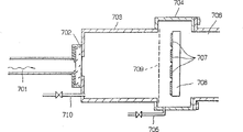
For making comparisons, the method for the formation microwave plasma that always uses so far is described at first.Fig. 7 is the diagrammatic sectional view of known microwave CVD apparatus structure.
Express a square waveguide 701 among Fig. 7 respectively, microwave introduction window 702, plasma generation chamber 703, film forming room 704, air supply pipe 705,710, exhaust outlet 706, thing 707 to be processed, object support 708 and wire netting assembly 709.
As shown in Figure 7, this device comprises plasma generation chamber 703 and uses the film forming room 704 of plasma, and both with wire netting assemblies 709 separately and control it and penetrate and make microwave and charged particle can not directly enter film forming room 704.Plasma generation chamber 703 has structure of resonant cavity, and the microwave by square waveguide 701 is by such as quartzy (SiO
2), aluminium pottery (Al
2O
3), the microwave introduction window 702 that teflon dielectric materials such as (teflon) constitutes is sent into plasma generation chamber.Thing 707 to be processed is placed in the film forming room 704, and there is the exhaust outlet 706 of air supply pipe 705 and find time plasma generation chamber 703 and film forming room 704 this chamber.
The plasma generating device one that constitutes like this starts, microwave is input to plasma generation chamber from square waveguide 701, hydrogen etc. are transformed into plasma by the electric field energy of microwave after introducing by gas introduction port 710, form the hydrogen atom that is in excitation state in a large number.The hydrogen atom of excitation state enters film forming room 704 by wire netting assembly 709, there they with from the gas collisions of air supply pipe 705, and produce chemical reaction, thereby on thing 707 to be processed, form deposited film.
But have in the common microwave plasma generation device of said structure in use, if square waveguide 701 clamps with plasma generation chamber 703 as resonant cavity, then do not match owing to input impedance, the problem that can exist most of microwave electric field to be reflected, thereby can not effectively utilize energy.
As a kind of solution of this problem, used a kind of method (referring to the open 55-141729 of Japan Patent) that electromagnet is obtained ECR (electronics widely different road resonance) around the resonant cavity arrangement.But because need be in this method up to 875 Gausses' magnetic density, so device is very big also very heavy.And this chamber is designed to normally constitute in a vacuum resonant cavity.Thus, if by the discharge generation plasma, then because of the plasma refraction rate less than 1, its just do not recur effect (compiling " discharge handbook ", the 4th part, chapter 2,298 pages) of resonant cavity referring to electric association.In addition, in the situation that forms magnetostatic field by electromagnet, because coil heats changes electric current, so when suppressing this change, not only need the long duration stably to prepare ECR condition (promptly high magnetic density) to 875 Gausses, and if depart from the ECR condition, will reduce the microwave absorbing rate, and before electric field is stable, be difficult to improve the service efficiency of electric field.
Therefore the present inventor finds that following design is the effective means that overcomes the problems referred to above, whether a kind of plasma exists and how density can both play the structure of resonant cavity effect no matter promptly design, and settles a bell jar to be used for exciting the TM film as plasma generation chamber in resonant cavity.
Particularly, in resonant cavity, a movable Cylinder that changes cavity length is installed, square waveguide and garden post resonant cavity clamp mutually and make their axle orthogonal, as shown in Figure 1.And in order to carry out impedance matching, be to use an obligatory point of the coupling part between square waveguide and resonant cavity preferably, perhaps the movable garden post with the change cavity length combines the E-H tuner of settling, perhaps any one in the three tap tuners.
Be placed on the bell jar that is used for forming plasma in the resonant cavity and can allow microwave penetrating, and by keeping airtight material to make, for example so-called new ceramic is such as quartzy (SiO
2), alum clay pottery (Al
2O
3), boron nitride (BN), silicon nitride (Si
3N
4), carborundum (SiC), beryllium oxide-(BeO), magnesium oxide (MgO) and zirconia (ZrO
2) etc.
The movable garden post that changes cavity length is placed facing to bell jar in a side of introducing microwave, promptly in atmospheric pressure one side.Therefore, because can change cavity length in atmosphere realizes impedance matching, so whether cavity length can easily exist by plasma or since the change of the cavity resonance condition that the change of plasma density causes adjust, thereby guarantee to produce microwave plasma with good repeatability and stability.
In the present invention, the wire netting assembly places between bell jar and the film formation space, work to form an end plate of chamber resonance condition, thereby the diameter of netted assembly is better less than λ/2, is more preferably 1/4 (λ/4) less than used microwave wavelength in the pipe.
Wire netting assembly shape such as metal are advised, i.e. metal sheet of having beaten a lot of holes square or garden shape, and it can be made by metal material, as Al, Fe, Ni, Ti, No, W, Pt, Au, Ag and stainless steel, or the above-mentioned metal sputtering in surface, the glass that gas deposition etc. were handled, pottery etc., or metallic composite.
And, for the excitation state hydrogen atom that forms is effectively also introduced film formation space equably, need to change the pore size distribution and the bore dia of wire netting assembly in bell jar.It is 10% better that whole porosity is equal to or greater than, and is equal to or greater than 20% better, preferably equals greater than 30%.
Even for the thickness that makes the deposited film that forms on the substrate among the present invention, the character unanimity has been investigated spacing between substrate and the wire netting assembly and wire netting assembly with respect to the angle of trunnion axis, obtains following result thus.
Fig. 3 (1) has provided two exemplary, each all illustrates the relation of the deposition of formation deposited film for the distance between substrate and the wire netting assembly, wherein curve a represents with " o " point, curve b forms with " " point, and they obtain in the membrance casting condition (A) shown in the table 1 (1) with (B) respectively.
Fig. 4 (1) representative when the angle variation of substrate and wire netting assembly, be deposited on on-chip, the thickness distribution of the film of expressing with the form that deposits rate variance.This is under membrance casting condition (A), and the distance between substrate and the wire netting assembly is to obtain in 40 millimeters (curve C is represented with " ▲ ") and 80 millimeters (curve d represents with " △ ") times.
Fig. 3 (2) illustrates two exemplary, and each all illustrates the relation of the deposition rate of formation deposited film for the distance between substrate and the wire netting assembly.Wherein curve a represents that with " o " some curve b puts expression with " ", and they obtain in the membrance casting condition (A) shown in the table 1 (2) with (B) respectively.Fig. 4 (2) representative is deposited on the thickness distribution of the film of expressing with the form of deposition rate difference on the substrate when the angle between substrate and the wire netting assembly changes.This is under membrance casting condition (B), and the distance between substrate and the wire netting assembly obtains when being 30 millimeters (curve C is with " ▲ " expressions) and 70 millimeters (curve d is with " △ " expressions).
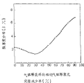
Can see from Fig. 3 (1) and 3 (2), when substrate and wire netting assembly when increasing, deposition rate is tending towards reducing rapidly.Under membrance casting condition (A),, almost can not form deposited film especially if distance surpasses 100 millimeters.Under membrance casting condition (B), when distance surpassed 100 millimeters, the deposited film characteristics of formation was also very poor, is unsuitable for practical application.In addition, see that when spending above 30 as if the angle of substrate and wire netting assembly, to all locational substrates, the distribution of film thickness increases sharply from Fig. 4 (1) and 4 (2), correspondingly, the also hurried variation of the distribution of film character, thus its uniformity significantly reduced.
Table 1 (1) project membrance casting condition (A) is 220 ℃ of compound S i that contain tetrels of substrate temperature (B)
2F
6The hydrogen atom H of 10sccm constitutive material gas
250sccm
The aluminium sheet (100 mm dia) of pressure 0.02 torr 0.04 torr wire netting assembly perforation during Ar 150sccm film forming
6 millimeters in aperture
Porosity 45%
Pore size distribution evenly is equally distributed on 8 positions the compound that contains tetrels, and the ring-type in 2 millimeters gas release device aperture discharges ring, from wire netting
250 watts 350 watts of assembly 10 millimeter microwave input powers
Table 1 (2)
(A) (B) 250 ℃ 250 ℃ compounds of substrate temperature (1) Si
2F
610sccm Si
2F
610sccm compound (2)
*GeF
410sccm GeF
4The H of 10sccm constitutive material gas
210sccm H
2Pressure 0.05 torr 0.15 torr wire netting assembly aperture during 10sccm hydrogen atom Ar 200sccm Ar 200sccm film forming: 6 millimeters apertures: 6 millimeters
Distribution evenly is evenly distributed
Porosity: 45% porosity: 30%
Aluminium: 120 mm dia aluminium: 120 mm dias discharge the gas release device aperture that the ring hoop discharges ring to compound (1) and (2) hoop: 2 millimeters * 8 apertures: 2 millimeters * 8
(equidistantly) (equidistantly)
Apart from 10 millimeters of wire nettings apart from 250 watts 300 watts of wire netting 10 millimeter microwave input powers
*) compound (2) is with the dilution of 10% helium.
Under several conditions, also carried out investigation same as described above, all obtained identical in fact result in each situation to forming other the 4th family semiconductive thin film.
Therefore in the present invention, the distance of substrate and wire netting assembly is decided to be 100 millimeters or nearer better, preferably 70 millimeters or nearer, angle 30 degree between the trunnion axis of substrate and wire netting assembly or littler better, 20 degree or littler preferably, these are the character of film thickness and distribution and film character uniformity to be remained on ± 5% interior necessary condition.
In addition to be used among the present invention tetrels compound or compound (1) and (2) and if necessary, be used to contain the element that can control valence electron and carried out further investigation as the gas release device of the compound of constituent, film thickness distributes and the uniformity of film character to improve.
Pressure limit said viscous in fluid technique flows and the zone of molecule between flowing preferably in the present invention, at this moment can not use the conduction computing formula that belongs to the molecule flow range.Therefore done following experiment in the present invention, noted pore size, the distance and the distribution in the gas release hole on the gas release device have obtained Fig. 5 (1) thus, and 5 (2) and Fig. 6 (1), 6 (2) result.
Fig. 5 (1) illustrates the result who forms deposited film in the membrance casting condition (A) of table 1 (1) down, and the substrate distance is 40 millimeters, has used the gas release ring 201 shown in Fig. 2 (a).Fig. 5 (2) then illustrates the result who forms deposited film in the membrance casting condition (A) of table 1 (2) down, 30 millimeters of substrate distances, and gas release ring 201 is shown in Fig. 2 (a).
In the gas release ring 201 shown in Fig. 2 (a), 8 release aperture 201a-201d, the equidistant configuration of 201a '-201d ', wherein the aperture is from release aperture 201a, the 201a ' hole 201d downstream of the most close arrow (→) direction, and 201d increases gradually.Fig. 5 (1) and 5 (2) has illustrated the variation that the thickness of deposited film that forms distributes when using the varying aperture rate as each gas release ring of 0-80%.
Can see that from the result be improved though change to film thickness distribution in 40% o'clock in the aperture increment rate from 0, if it surpasses 40%, film thickness distributes and increased, if it has surpassed 60%, (aperture increment rate 0%) went back big when the film thickness distribution was more constant than the aperture.Film character distributes relevant with film thickness in fact.Under other membrance casting condition, trend in fact also is the same.
Therefore in the present invention, be to make the aperture increment rate between 0-50% preferably, better between 20-40%.
Then, Fig. 6 (1) and 6 (2) be with top same membrance casting condition under, with the experimental result of gas release ring 202 shown in Fig. 2 (6).
In the gas release ring of Fig. 2 (b), the release aperture 202a-202d that 8 same apertures are arranged on the ring, its mutual spacing of 202a '-202d ' reduces between 202a ' distance gradually with respect to release aperture 202a, and the change that the thickness of deposited film that each the gas release ring that changes from 0-70% with slip forms distributes is shown in Fig. 6 (1) and 6 (2).
Though can see when aperture spacing slip when 0-40% changes, film thickness distributes and has improved, but if surpass 40%, film thickness distributes have been increased, if surpass 50%, film thickness distributes and further is increased to the situation of aperture distance constant (aperture spacing slip 0%).
The character of film is expressed in fact and is distributed relevant with film thickness.Under other membrance casting condition, trend is also the same in fact.
Therefore in the present invention, it is better that aperture spacing slip is located at 0-50%, better from 20-40%.
But also carried out with Fig. 5 (1) experiment of same definite relation shown in 5 (2) with the gas release ring 203 of Fig. 2 (c).In gas release ring 203 shown in Fig. 2 (c), release aperture is equally distributed, and the aperture increases from 203a to 203d successively.It is the same with result shown in Fig. 5 (1) and 5 (2) in fact with the change trend of the character of film that the film thickness that obtains with the gas release ring of different increment rates distributes.
When therefore the gas release hole distributed shown in Fig. 2 (c) in the present invention, the aperture increment rate was better in the 0-40% range, and is better in the 10-30% scope.
In the present invention, become the internal pressure of mem stage suitably to determine according to the film forming situation, this film forming situation depends on the condition that stably forms microwave plasma from the admixture of gas of hydrogen or hydrogen and inert gas composition, depend on selected compound that contains tetrels or compound (1) and (2) and can control the state and the kind of the compound (3) of valence electron, and the character of the deposited film that requires etc.Internal pressure is located at 100 torrs-1 * 10
-4Torr is better, 10 torrs-5 * 10
-4Torr is better, preferably 1 torr-1 * 10
-3Torr.
Use method of the present invention, can on any crystalline substrate, form required crystallinity deposited film, no matter its noncrystal or crystalline nature how.
In the present invention, in order to set up stable chamber resonance condition, adopt the continuous oscillation mode, the fluctuating scope of used power is better in 30% scope.
Use method of the present invention, there is the hydrogen atom of good controllability, stability and repeatable excitation state to form with the microwave plasma of the resonant cavity that combines with two impedance matching loops in the microwave circuit, thereby improved the controllability of excitation state hydrogen atom and film forming starting compound reaction significantly, tetrels semiconductive thin film with required crystallinity and hydrogen content etc. can be with good uniformity, and the repeatability that high efficiency is become reconciled forms.
To be described an exemplary embodiments that is suitable for implementing the deposition membrane formation device of the inventive method, but should point out that the present invention is not limited in this deposition membrane formation device.
Fig. 1 is the structure diagram that explanation is suitable for implementing the deposition membrane formation device of the inventive method.
In Fig. 1, garden cylindricality resonant cavity 101 comprises a microwave plasma generating chamber bell jar 102.103, one 104, one square wave conduits 108 of movable garden post and main element such as constrainer 110 that change cavity length of a wire netting assembly.The spring 105 that phosphor bronze is done is used for contacting of improvement activity garden post 104 and garden post resonant cavity 101, to prevent abnormal discharge.Available motor 106 moves and changes long 104, one change-speed gearings 107 of movable cylinder in chamber towards bell jar 102.E-H tuner or three tap tuners 109 are formed the impedance matching loop that constitutes a microwave circuit in the present invention, and it is to be used for using do impedance matching with movable garden post 102 pairings as the change resonant length in another impedance matching loop.Constrainer 110 constitutes one of impedance line with the same manner, and it uses in pairs with the movable garden post 102 that changes cavity length.
The release aperture of the admixture of gas of hydrogen that discharges gas inlet pipe 111 or hydrogen and inert gas is by the wire netting assembly and point to the inside of bell jar 102.The microwave that the hydrogen of input bell jar etc. is added on the resonant cavity 101 converts plasma to form excitation state hydrogen atom etc.Enter film formation space 116 by wire netting assembly 103 then.The pressure of film formation space is measured with pressure gage 125.
At film formation space 116, the release ring that forms deposited film unstrpped gas is placed between substrate 118 and the base sheet rack 119.
When introducing preactivate film forming unstrpped gas, transport the diameter of pipe 117 and the activated state that its material should be able to be kept this gas.
The film forming unstrpped gas of introducing film formation space 116 etc. is extracted out with unshowned aspiration pump according to direction shown in the arrow among the figure.
To describe in more detail according to deposited film formation method of the present invention with reference to following example.But should be noted that the present invention is not limited only to these examples.
Example 1
At first the glass substrate 118 of a diameter 150 (merchant's trade mark: 7059, Corning Glass Works makes) is placed on the base sheet rack 119 of film formation space 116, with unshowned aspiration pump film formation space pressure is dropped to 1 * 10
-6Torr.Heated substrate support then.Make the substrate surface temperature fix on 220 ℃ with unshowned substrate temperature controller.
After the substrate surface temperature is determined, introduce the hydrogen of 20sccm and the argon gas of 100sccm by gas inlet pipe 111 to quartz bell cover 102 from unshowned gas source.With automatic pressure controller pressure in the film formation space 116 is controlled at 0.1 torr then.
Import microwaves by square waveguide 118 to resonant cavity 101 from unshowned continuous oscillation type microwave oscillator then.After this very fast is reflection power/incident power ratio that the movable cylinder 104 that changes cavity length is adjusted to by the measurement of the power monitor in the unshowned microwave line minimum position with motor 106 and change-speed gearing 107, and the stretching degree of further regulating constrainer 110 makes the ratio of reflection power/incident power for minimum.Repeat fine tuning then and change the position of movable cylinder 104 of cavity length and the stretching degree of constrainer 110, make reflection power one incident power, make effective incident power of incident power/reflection power representative be placed on 200 watts than minimum.
In this example, the hydrogen atom excitation state line of departure H that monitors by hole 121
αThe strength ratio of/Hp is 120.
The distance of substrate 108 and wire netting assembly 103 is that 40 millimeters and the two are parallel to each other.As wire netting assembly 103, the diameter in hole is 8 millimeters by 150 millimeters aluminium sheets with holes of diameter, and porosity is 80% and evenly distributes.Gases used release ring is just like structure shown in Fig. 2 (a), and wherein the aperture corresponding to 201a and 201a ' is 1.5 millimeters, and the aperture increases than being 30%.
Then the Si of 10sccm
2F
6The BF of gas and 5sccm
3(use SiF
4Be diluted to 200/1000000ths (200ppm)) mixture enter film formation space 116 from unshowned gas source by air supply pipe 120 input and from gas release ring 112, under this situation, pressure controller maintains 0.1 torr to the pressure in the film formation space automatically.BF
3Also play a part dopant.
Very fast hydrogen atom and the Si that in 60 minutes, on substrate, forms by excitation state
2F
4, BF
3Chemically reactive forms the Si of 4.2 micron thickness: H: F: B film (1-1 sample).
Substrate is taken out in the cooling back, with the n of-6 English inch
+Si (110) chip replaces it, with above-mentioned same step, and except changing hydrogen flowing quantity to 150sccm, microwave input power to 350 watt, film formation space pressure is to 0.02 torr, substrate temperature to 280 ℃, formation deposited film.H α/Hp strength ratio is 40 (1-2 samples) in this case.
When the film thickness of each the deposited film sample that obtains with X-ray diffractometer and electron ray diffractometer (RHEED) distributes with its crystallinity, point out that each sample film thickness distribution is within ± 3%, the 1-1 sample is an amorphous film, and the 1-2 sample be parallel to substrate surface have almost (110) orientation outer place prolong film.
Each sample is placed in the vacuum deposition apparatus, comb type aluminium electrode with 250 microns gaps is made gas deposition with the point-like electrode of 2 mm dias that are heated by resistive, conductivity (δ) (δ p: the light conductance, δ d: dark conductivity) and hole mobility (μ h) with ten thousand, moral.The bohr method is measured.The value of the δ p/ δ d of 1-1 sample is 4.5 * 10
5(δ p: be the value under the AM-1 irradiation) is 450 ± 13cm to the value of μ h in the whole surface of 1-2 sample
2/ weber, its characteristic distribute be approximately ± 3%.And checking that with the thermovoltaic power measurement its conduction type shows, they all are the p-types.
And when measuring hydrogen content with SIMS, atomic percent is 9% in the 1-1 sample, and atomic percent is 0.08% in the 1-2 sample.
Can find that from aforementioned crystallinity is easy to control according to the present invention.
Example 2
Except that microwave input power is transferred to 150 watts and 250 watts and is done 114 to 700 ℃ of the activation spaces that quartz ampoule that the heating of activation energy generation device places air supply pipe 120 surrounds with infrared heating furnace from 200 watts and 350 watts, to form deposited film (2-1 number and 2-2 sample) with the same step of example 1.
To the 2-1 sample, film forming inch H α/H β is 155, is 60 to the 2-2 sample.
When the same step of use-case 1 was identified the deposited film that obtains, though microwave input power has reduced, it is about 10% that deposition has increased, and obtain and the essentially identical character of example 1 sample, as shown in table 2.
Example 3
Except substrate is used glass substrate (commercial name: No. 7059 instead, Corning Glass Works makes), it is 0.06 torr that film formation space pressure is set, outside 250 ℃ of the substrate temperatures, form deposited film under same step that sample 1-2 forms in example 1 and the same formation condition, H α/Hp is 70 during film forming.
When deposited film being measured its film thickness distribution and crystallinity with x-ray diffractometer and electron diffraction instrument (RHEED), prove this film thickness be distributed in ± 3% within, it is-polycrystalline film, is almost (110) in the orientation that is parallel to substrate surface, and mean particle size is 1.2 microns.The atomic percent of hydrogen content is 1.2%.
Hole mobility is determined as 45 ± 1.3cm
2/ weber, conduction type is the p-type.
Example 4-example 6
Except change over membrane material compound and a part of membrance casting condition as shown in table 3, in example 1, form deposited film under same step and the membrance casting condition.
When measuring gained deposited film character, the result as shown in table 4 they be film thickness and the high-quality film of film property distribution within ± 3%.
Example 7
At first, the glass substrate of 150 millimeters of diameters (commercial product: No. 7059, make between the corning glass public affairs) is placed on the base sheet rack 119 of film formation space 116, the pressure of film formation space is extracted into 1 * 10 with unshowned air exhauster
-6Torr.Then, the heated substrate support makes the substrate surface temperature be arranged on 230 ℃ with unshowned substrate temperature controller.
After the substrate surface temperature is determined, 20sccm hydrogen and 200sccm argon gas are delivered to quartz bell cover 102 from unshowned air accumulator by gas inlet pipe 111.With unshowned automatic pressure controller the pressure of film formation space 116 is controlled at 0.2 torr subsequently.
Then, by square waveguide 118 microwave is guided to resonant cavity 101 from unshowned continuous type microwave oscillator.In the near future, with with reach 106 and change-speed gearing 107, be adjusted to the position that reflection power/incident power ratio of being measured by the power monitor in the unshowned microwave circuit is minimum changing the long movable cylinder in chamber, the stretching degree of regulating constrainer 110 then makes the ratio of reflection power/incident power for minimum, repeat fine tuning then and change the position of the long movable cylinder 104 in chamber and the stretching degree of constrainer 110, make reflection power/incident power than minimum, make effective incident power of incident power/reflection power representative be placed on 350 watts.
In this embodiment, the strength ratio of the hydrogen atom excitation state line of departure H α/Hp that monitors by hole 121 is 200.
Subsequently the Si of 10sccm
2F
6Gas and with the GeF of diluted in hydrogen to 10%
4Gas is imported by air supply pipe 120 from unshowned gas source, and sends into film formation space 116 by gas release ring 112.In this case, the pressure in the film formation space 116 is maintained 0.2 torr by automatic pressure controller.
Soon, at the hydrogen atom and the Si of excitation state
2F
6, GeF
4The gas chemically reactive formed the film of 7.5 micron thickness on substrate in 60 minutes.Take out as the 7-1 sample substrate cooling back.
Except with one 6 English inch n
+Si (110) chip makes substrate and hydrogen flowing quantity is 10sccm, and the Ar throughput is 50sccm, and film formation space pressure is 0.01 torr, and the porosity of perforated plate is outside 30%, forms deposited film with above-mentioned same step, and strength ratio H α/Hp was 40 (being called the 7-3 sample).The film thickness that measures each deposited film with X-ray diffractometer and electron ray diffractometer (RHEED) distributes and its crystallinity.Each sample all has good uniformity, and points out that the 7-1 sample is an amorphous, and the 7-2 sample is a polycrystalline film, and the 7-3 sample is to be parallel to the epitaxial film that substrate surface has almost (110) to be orientated.
In addition, each sample is downcut a part, with its composition of sims analysis.The content of hydrogen is pressed 7-1 number, and 7-2 number, the order of 7-3 sample is by subtracting.
Each sample is put in the vacuum deposition apparatus, and the aluminium point-like electrode that the diameter by resistance heating is 2 millimeters carries out gas deposition, measures hole mobility (μ h) with ten thousand moral bohr methods.On the whole sample surface, the characteristic distribution error the results are shown in Table 5 within ± 3%.
From then on the result can see the crystallinity that is easy to control deposited film according to the present invention.
Example 8
Form a kind of Si: Ge: H by example 1 same step under the following conditions: the F film.Remove and make GeF
4Gas flow is to form film under the external condition same with making example 7 samples 1 of 5sccm.(being called the 8-1 sample)
Remove then and establish GeF respectively
4Gas flow is 7sccm, outside 12sccm and the 15sccm, divides making film (being called 8-2,8-3,8-4 sample) 3 times in same mode.
Identify that with X-ray diffractometer and electron ray diffractometer (RHEED) film thickness of the deposited film sample that each obtains distributes and crystallinity, illustrated that the uniformity of each sample is fine and all be amorphous film.
Secondly, downcut a part, with its silicon of sims analysis and germanium composition ratio from each sample.Survey the absorption spectra of each sample to make the luminous energy band gap with visible spectrophotometer more subsequently.And then each sample placed vacuum deposition chamber, carry out gas deposition with comb type clearance electrode (250 microns of gap lengths, wide 5 millimeters).Measure the dark conductivity under 10 volts of voltages, then with AM-1 light (100 milliwatt/square centimeter) irradiation decision light conductance and determine the ratio of dark conductivity and light conductance thus.Each character in whole plane all within ± 3%.The above results sees Table 6.From found that, SiGe composition ratio can change selectively by changing gas flow, and the luminous energy band gap also can be controlled to such an extent that be formed with the deposited film of required character.
Can see that from the result blooming character of deposited film can easily be controlled by the present invention.
Example 9
Except that making hydrogen flowing quantity is that 50sccm and microwave input power are 300 watts, as following condition under, by the same step formation-Si of example 7: C: H: F film.Glass substrate (No. 7059) with one 150 mm dia is used as substrate, is flow the Si of 20sccm
2F
6Gas and flow are the CH of 10sccm
4Gas is sent into film formation space, and film formation space pressure is 0.2 torr, and substrate temperature is 260 ℃.With the gas release ring same with example 1, wire netting assembly and substrate position, the time that forms film is 60 minutes,
Then except increasing the BF that is diluted to 10% 10sccm with helium
3Form film with as above same step outward.Under each situation, α/the Hp ratio was 180 (being called 9-1 number, 9-2 sample) to H when film formed.
Be 100sccm and interior pressure 0.03 torr except making hydrogen flowing quantity then, with the step formation film (be called 9-3 sample) same with the 9-2 sample.
To each its crystallinity of the sample identification that obtains like this and hydrogen content, so in the use-case 7 same mode calorimetric voltaic power to judge conduction type.From each sample, downcut a part respectively, put into vacuum deposition chamber, carry out gas deposition with comb type aluminium clearance electrode (250 microns of gap lengths, wide 5 millimeters).Measure the dark conductivity under 10 volts then, photometry conductance under AM-1 light (100 milliwatt/square centimeter) irradiation determines dark conductivity and light conductance ratio thus again.Each properties of samples is within ± 3% on whole plane.Gained the results are shown in Table 7.
From The above results as can be known, the conduction type of deposited film and electrical mass-energy are easily controlled by the present invention.
Example 10
Except microwave input power is changed to 200 watts and with activation energy generation device infrared heating furnace the activation space 114 that the quartz ampoule above the air supply pipe 120 constitutes is heated to 700 ℃ from 350 watts, adopt with the same step of example 7 and form deposited film.
At first making substrate with 7059 flint glass Fs and make hydrogen flowing quantity is 100sccm, and interior pressure is to form film (being called the 10-1 sample) under the 0.05 torr condition.Then, make substrate with 6 inch n+Si chips, making hydrogen flowing quantity is 20sccm, and formingspace pressure is under 0.01 torr (the being called the 10-2 sample) condition, forms another film.
When the deposited film that obtains like this with example 7 in same mode when identifying, though microwave input power reduces, deposition does not reduce, obtained with example 7 in essentially identical character, the results are shown in table 8.
Example 11
Except changing over pleurodiaphragmatic in terspace material compound and a part of membrance casting condition of change as shown in table 9.With same membrance casting condition of example 7 and same step under form deposited film.
The film that obtains is like this identified with step same in the example 9, is obtained result as shown in table 10.
Example 12
Removing and making hydrogen flowing quantity is 50sccm, and microwave input power is 200 watts, and under the following condition, forms Si: C: H with step same in the example 7: the F film.
Flow is the SiF of 20sccm
4Gas and flow are the SiH of 5sccm
4The mixture of gas is as first unstrpped gas, and flow is the CF of 10sccm
4As second unstrpped gas, they are introduced into film formation space, and film formation space pressure is 0.03 torr, and substrate temperature is 200 ℃.The porosity of wire netting assembly be 30% gas release ring with substrate sections and example 1 in the same.H α during film forming/H β ratio was 100 (being called 12-1 number, 12-2 sample).
Identify the sample that obtains by step same in the example 9, obtain the result shown in the table 11.
Each character shows that all distributing homogeneity in this plane is ± 3%.
Table 2
Table 3
| Example | Starting compound and flow rate | The change of |
| 4 | GeF
4 10sccm PF
5(arriving 500ppm) 5sccm H with HD
2/ | Microwave power 250W H α/H β=140 glass substrates; 180 ℃ of #7059 pressure 0.08 |
| 5 | GeF
4/Ge(450℃)10Sccm BF
3(being diluted to 800ppm) 5sccm H with helium
2/ | 250 ℃ of microwave power 250W H α/H β=200 n+Si wafer pressure 0.03Torr substrate temperatures |
| CH 3F 15sccm H 2/He 250/50sccm | 300 ℃ of microwave power 350W H α/H β=35 non-doped silicon wafer pressure 0.005torr substrate temperature |
Table 4
| Example | Film quality | Hydrogen | Film character | |
| 4 | Amorphous Ge: H: F: P | 21 atomic percent % | μe1.5cm
2/ v.sec n- | |
| 5 | Extension Ge: H: F: B | 0.05 atomic percent % | μn3500cm
2/ v.sec p- | |
| 6 | Class diamond C: H: F | 0.08 atomic percent % | Mohs' hardness>9 |
Table 5
| Sample number | 7-1 | 7-2 | 7-3 |
| Film quality | Si∶Ge∶H∶F | Si∶Ge∶H∶F | Si∶Ge∶H∶F |
| Crystallinity | Armorphous | Polymorphic | Extension type |
| Hydrogen content | 10.5% | 3.5% | 0.5% |
| Hole mobility | 0.8cm 2/v.sec | 65cm 2/v.sec | 1200cm 2/v.sec |
| Conduction type | Intrinsic | Intrinsic | Intrinsic |
Table 6
| Sample number | 8-1 | 8-2 | 8-3 | 8-4 |
| GeF 4Flow rate | 5sccm | 7sccm | 12sccm | 15sccm |
| Si: the Ge composition is than (atomic percentage) | 86∶14 | 79∶21 | 70∶30 | 61∶39 |
| The luminous energy band gap | 1.65eV | 1.60eV | 1.53eV | 1.44eV |
| δp/δd | 4.0×10 5 | 9.2×10 4 | 3.3×10 4 | 1.8×10 4 |
Table 7
| Sample number | 9-1 | 9-2 | 9-3 |
| Film quality | Si∶C∶H∶F | Si∶C∶H∶F | Si∶C∶H∶F |
| Crystal type | Armorphous | Armorphous | Polymorphic |
| Hydrogen content | 12.5% | 10.8% | 4.5% |
| δp/δd | 5.5/×10 4 | 6.2×10 4 | 3.9×10 2 |
| Conduction type | Intrinsic | The p-type | The p-type |
Table 8
| Sample number | 10-1 | 10-2 |
| Film quality | Si∶Ge∶H∶F | Si∶Ge∶H∶F |
| Crystal type | Polymorphic | Extension type |
| Hydrogen content | 10.5% | 3.5% |
| Hole mobility | 62cm 2/v.sec | 1220cm 2/v.sec |
| Conduction type | Intrinsic | Intrinsic |
Table 9
| Sample number | Unstrpped gas and flow rate | Membrance casting condition |
| 11-1 | SiF
4 30sccm C
2H
2 5 ″ | Microwave power 280W is introduced in and activates the SiF that activates with radio frequency discharge (10W) in the chamber 4 |
| 11-2 | SiH
2F
2 30sccm SnF
4 20 ″ | Microwave power 200W pressure 0.65Torr |
| 11-3 | SiH
2Cl
230sccm SnCl
4 10 ″ | Microwave power 280W pressure 0.15Torr |
Table 10
| Sample number | 11-1 | 11-2 | 11-3 |
| Film quality | Si∶C∶H∶F | Si∶Sn∶H∶F | Si∶Sn∶H∶F |
| Crystal type | Amorphous | Amorphous | Amorphous |
| Hydrogen content | 9.8% | 7.6% | 8.1% |
| δp/δα | 2.5×10 4 | 3.8×10 2 | 2.8×10 2 |
| Conduction type | Intrinsic | Intrinsic | The p-type |
Table 11
| Sample number | 12-1 | 12-2 |
| Film quality | Si∶C∶H∶F | Si∶C∶H∶F |
| Crystallinity | Polycrystalline | Extension |
| Hydrogen content | 2.5% | 0.02% |
| δp/δd | 8.5×10 2 | 3.2 |
| Conduction type | Intrinsic | Intrinsic |
Claims (18)
1. method that forms functional deposited film, introduce the compound that belongs to the periodic table tetrels as containing of film forming raw material by film formation space to the substrate place that forms deposited film thereon, and, if desired, introducing contains the element that can control the deposited film valence electron compound as constituent, formation contains the functional deposited film of periodic table the 4th family's atom as main composed atom, each compound become gaseous state or at least compound be the state of preactivate in the activation space that separates with described film formation space, form the excitation state hydrogen atom simultaneously, they and at least a described gaseous state or in being different from the activation space of described film formation space, be in compound chemically reactive activated state and that be introduced into film formation space, thereby on described substrate, form deposited film, it is characterized in that:
Described excitation state hydrogen atom is the microwave plasma that produces with in the plasma generation chamber in the microwave circuit and the resonant cavity that two impedance matching loops combine, the gaseous mixture of forming from hydrogen or hydrogen and an inert gas forms, described plasma generation chamber comprises the bell jar of a wire netting assembly and permeable microwave, and connect together by described wire netting assembly and described film formation space, and the excitation state of hydrogen atom is controlled.
2. according to the method for the formation functional deposited film of claim 1, wherein the excitation state of hydrogen atom is to control than H α/H β by the emissive porwer of measuring hydrogen atom excitation state with emission spectrophotometry method, and the microwave power of its resonant cavity is supplied with in control, the impedance matching condition, the flow rate of the gaseous mixture of hydrogen gas rate or hydrogen and inert gas and at least one parameter in the total pressure are to obtain the desirable value of described strength ratio.
3. according to the method for the formation functional deposited film of claim 1 or 2, wherein the impedance matching loop in the resonant cavity that combines with two impedance matching loops in microwave circuit is to place the movable cylinder that changes cavity length or place waveguide and the restraint device of resonant cavity coupling part, comes the control group matching circuit by adjusting these devices.
4. according to the method for the formation functional deposited film of claim 3, wherein the impedance matching loop is movable cylinder and an E-H tuner or one the three tap tuner that changes resonant cavity.
5. according to the method for the formation functional deposited film of claim 1, wherein the hydrogen atom of excitation state is introduced film formation space by the wire netting assembly.
6. according to the method for the formation functional deposited film of claim 1, wherein substrate becomes 30 ° of degree angles or littler with respect to wire netting surface level axle, and surperficial with described wire netting at a distance of in 100 millimeters, gaseous state or activated state compound are introduced film formation space from placing the gas release device between described wire netting surface and the described substrate.
7. according to the method for the formation functional deposited film of claim 6, wherein gas release device is installed in around the substrate ringwise, the last release aperture that interval between the gas release hole described gas release device from introducing gas one side direction reduces gradually, makes the gas release amount of coming from each gas release hole even.
8. according to the method for the formation functional deposited film of claim 6, wherein gas release device is installed in around the substrate ringwise, the last release aperture that the aperture in gas release hole described gas release device from introducing gas one side direction increases gradually, makes the gas release amount of coming from each gas release hole even.
9. according to the method for the formation functional deposited film of claim 6, wherein the gas release hole of gas release device evenly distributes in substrate plane at least, the middle body that the aperture in each gas release hole described gas release device from introducing gas one side direction increases gradually, makes the gas release amount of coming from each gas release hole even.
10. method that forms functional deposited film, by introducing compound (1) that contains silicon and the compound of representing with following formula (1) as the film forming raw material (2) to the film formation space at the substrate place that forms deposited film thereon, and, if desired, introducing contains the element that can control the deposited film valence electron compound (3) as constituent, formation contains the functional deposited film of silicon atom and the main composed atom of periodic table the 4th family atom conduct, each compound becomes gaseous state or becomes at least a compound is the state of preactivate in the activation space that separates with described film formation space, form the hydrogen atom of excitation state simultaneously, with be in described gaseous state or in the activation space that is different from described genus film space, be in described compound activated state and that be introduced into film formation space (1), (2) and at least a chemically reactive of (3), thereby on described substrate, form deposited film, it is characterized in that:
Described excitation state hydrogen atom is the microwave plasma that produces with in the plasma generation chamber in the microwave circuit and the resonant cavity that two impedance matching loops combine, the gaseous mixture of forming from hydrogen or hydrogen and a kind of inert gas forms, described plasma generation chamber comprises the bell jar of a wire netting assembly and permeable microwave, and connect together by described wire netting assembly and described film formation space, and the excitation state of hydrogen atom is controlled:
AaBb ... (I) wherein A represents the silica removal element that belongs to periodic table the 4th family in addition, the B representative is from hydrogen (H), a kind of composition that selects in halogen (X) and the hydrocarbon, a are represented a positive integer that equals valence mumber or this valence mumber integral multiple of B, and b represents a positive integer.
11. method according to the formation functional deposited film of claim 10, wherein the excitation state of hydrogen atom is by measuring the emissive porwer of hydrogen atom excitation state than H α/H β with emission spectrophotometry method, and the microwave power of resonance is supplied with in control, the impedance matching condition, the flow of the gaseous mixture of hydrogen gas rate or hydrogen and inert gas and at least one parameter in the total pressure are controlled, to obtain the strength ratio of described expection.
12. method according to the formation functional deposited film of claim 10 or 11, wherein the impedance matching loop in the resonant cavity that combines with two impedance matching loops in microwave circuit is to place the movable cylinder that changes cavity length or place waveguide and the restraint device of resonant cavity coupling part, controls matching status by adjusting these devices.
13. according to the method for the formation functional deposited film of claim 12, wherein the impedance matching loop is movable cylinder and an E-H tuner or one the three tap tuner that changes resonant cavity.
14. according to the method for the formation functional deposited film of claim 10, wherein the excitation state hydrogen atom is introduced film formation space by the wire netting assembly.
15. method according to the formation functional deposited film of claim 10, wherein substrate becomes 30 degree angles or littler with respect to wire netting surface level axle, and surperficial in 100 millimeters with described wire netting, film formation space is introduced from placing the gas release device between described wire netting surface and the described substrate in gaseous state or activated state compound (1), (2) and (3).
16. method according to the formation functional deposited film of claim 15, wherein gas release device is placed in around the substrate ringwise, the last release aperture that the interval in gas release hole described gas release device from introducing gas one side direction reduces gradually, makes the gas release amount of coming from each gas release hole even.
17. method according to the formation functional deposited film of claim 15, wherein gas release device is placed on around the substrate ringwise, the last release aperture that the aperture in gas release hole described gas release device from a side direction of introducing gas increases gradually, makes the gas release amount of coming from each gas release hole even.
18. method according to the formation functional deposited film of claim 15, wherein the gas release hole of gas release device evenly distributes in substrate plane at least, the middle body that the aperture in each gas release hole described gas release device from introducing gas one side direction increases gradually, makes the gas release amount of coming from each gas release hole even.
Applications Claiming Priority (5)
| Application Number | Priority Date | Filing Date | Title |
|---|---|---|---|
| JP2179888A JPH01198479A (en) | 1988-02-01 | 1988-02-01 | Formation of deposited film by microwave plasma cvd |
| JP21798/88 | 1988-02-01 | ||
| JP21799/1988 | 1988-02-01 | ||
| JP21798/1988 | 1988-02-01 | ||
| JP2179988A JPH01198480A (en) | 1988-02-01 | 1988-02-01 | Formation of deposited film by microwave plasma cvd |
Publications (2)
| Publication Number | Publication Date |
|---|---|
| CN1039680A CN1039680A (en) | 1990-02-14 |
| CN1031088C true CN1031088C (en) | 1996-02-21 |
Family
ID=26358903
Family Applications (1)
| Application Number | Title | Priority Date | Filing Date |
|---|---|---|---|
| CN89100622.2A Expired - Fee Related CN1031088C (en) | 1988-02-01 | 1989-02-01 | Process for forming functional deposited film |
Country Status (4)
| Country | Link |
|---|---|
| US (1) | US4908330A (en) |
| EP (1) | EP0334000B1 (en) |
| CN (1) | CN1031088C (en) |
| DE (1) | DE68917500T2 (en) |
Families Citing this family (35)
| Publication number | Priority date | Publication date | Assignee | Title |
|---|---|---|---|---|
| DE3786364T2 (en) * | 1986-04-14 | 1993-11-18 | Canon Kk | Process for producing a deposited layer. |
| US5221643A (en) * | 1989-02-21 | 1993-06-22 | Siemens Aktiengesellschaft | Method for producing polycrystalline semiconductor material by plasma-induced vapor phase deposition using activated hydrogen |
| US5214002A (en) * | 1989-10-25 | 1993-05-25 | Agency Of Industrial Science And Technology | Process for depositing a thermal CVD film of Si or Ge using a hydrogen post-treatment step and an optional hydrogen pre-treatment step |
| JPH0560242A (en) * | 1991-08-28 | 1993-03-09 | Japan Atom Energy Res Inst | Ceramic vacuum container and manufacture thereof |
| US5204272A (en) * | 1991-12-13 | 1993-04-20 | United Solar Systems Corporation | Semiconductor device and microwave process for its manufacture |
| US5975912A (en) * | 1994-06-03 | 1999-11-02 | Materials Research Corporation | Low temperature plasma-enhanced formation of integrated circuits |
| US5628829A (en) * | 1994-06-03 | 1997-05-13 | Materials Research Corporation | Method and apparatus for low temperature deposition of CVD and PECVD films |
| US5665640A (en) * | 1994-06-03 | 1997-09-09 | Sony Corporation | Method for producing titanium-containing thin films by low temperature plasma-enhanced chemical vapor deposition using a rotating susceptor reactor |
| WO1995034092A1 (en) * | 1994-06-03 | 1995-12-14 | Materials Research Corporation | A method of nitridization of titanium thin films |
| US6161500A (en) | 1997-09-30 | 2000-12-19 | Tokyo Electron Limited | Apparatus and method for preventing the premature mixture of reactant gases in CVD and PECVD reactions |
| US6313017B1 (en) | 1999-01-26 | 2001-11-06 | University Of Vermont And State Agricultural College | Plasma enhanced CVD process for rapidly growing semiconductor films |
| US6173673B1 (en) | 1999-03-31 | 2001-01-16 | Tokyo Electron Limited | Method and apparatus for insulating a high power RF electrode through which plasma discharge gases are injected into a processing chamber |
| US6743700B2 (en) * | 2001-06-01 | 2004-06-01 | Semiconductor Energy Laboratory Co., Ltd. | Semiconductor film, semiconductor device and method of their production |
| US7199027B2 (en) * | 2001-07-10 | 2007-04-03 | Semiconductor Energy Laboratory Co., Ltd. | Method of manufacturing a semiconductor film by plasma CVD using a noble gas and nitrogen |
| JP5072157B2 (en) * | 2001-09-27 | 2012-11-14 | 株式会社半導体エネルギー研究所 | Method for manufacturing semiconductor device |
| JP2003293128A (en) * | 2002-04-05 | 2003-10-15 | Canon Inc | Method for forming deposited film |
| US7205187B2 (en) * | 2005-01-18 | 2007-04-17 | Tokyo Electron Limited | Micro-feature fill process and apparatus using hexachlorodisilane or other chlorine-containing silicon precursor |
| DE102005024041A1 (en) * | 2005-05-25 | 2006-11-30 | City Solar Ag | Process for the preparation of silicon from halosilanes |
| DE102006043929B4 (en) * | 2006-09-14 | 2016-10-06 | Spawnt Private S.À.R.L. | Process for the preparation of solid polysilane mixtures |
| KR20100093347A (en) * | 2009-02-16 | 2010-08-25 | 엘지전자 주식회사 | Solar cell, method for manufacturing of solar cell and apparatus for manufacturing of solar cell, method for deposition of thin film layer |
| JP6071439B2 (en) | 2011-11-30 | 2017-02-01 | キヤノン株式会社 | Method for producing phthalocyanine crystal and method for producing electrophotographic photoreceptor |
| JP5993720B2 (en) | 2011-11-30 | 2016-09-14 | キヤノン株式会社 | Electrophotographic photosensitive member, process cartridge, and electrophotographic apparatus |
| JP5827612B2 (en) | 2011-11-30 | 2015-12-02 | キヤノン株式会社 | Method for producing gallium phthalocyanine crystal, and method for producing electrophotographic photoreceptor using the method for producing gallium phthalocyanine crystal |
| JP2017010009A (en) | 2015-06-24 | 2017-01-12 | キヤノン株式会社 | Electrophotographic photoreceptor, process cartridge, and electrophotographic device |
| DE102015115355B3 (en) * | 2015-09-11 | 2017-01-19 | Schunk Kohlenstofftechnik Gmbh | Heating chamber for analyzing contaminant levels in samples |
| US10095137B2 (en) | 2016-04-04 | 2018-10-09 | Canon Kabushiki Kaisha | Electrophotographic photosensitive member, method of producing electrophotographic photosensitive member, process cartridge, and electrophotographic image forming apparatus |
| PT109387B (en) * | 2016-05-13 | 2021-12-14 | Inst Superior Tecnico | PROCESS AND SYSTEM FOR THE SELECTIVE PRODUCTION OF AUTONOMOUS TWO-DIMENSIONAL NANOSTRUCTURES USING PLASMA TECHNOLOGY |
| JP6978858B2 (en) | 2016-06-21 | 2021-12-08 | キヤノン株式会社 | An electrophotographic photosensitive member, a method for manufacturing an electrophotographic photosensitive member, a process cartridge having the electrophotographic photosensitive member, and an electrophotographic apparatus. |
| CN106770144B (en) * | 2017-03-06 | 2024-04-09 | 清华大学 | Solid sample chemical vapor generation and sample injection method based on hydrogen plasma |
| KR102058865B1 (en) * | 2018-04-12 | 2019-12-24 | (주)아이엠 | Heating device using hyper heat accelerator and method for manufacturing the same |
| US11320754B2 (en) | 2019-07-25 | 2022-05-03 | Canon Kabushiki Kaisha | Process cartridge and electrophotographic apparatus |
| US11573499B2 (en) | 2019-07-25 | 2023-02-07 | Canon Kabushiki Kaisha | Process cartridge and electrophotographic apparatus |
| JP2021173806A (en) | 2020-04-21 | 2021-11-01 | キヤノン株式会社 | Electrophotographic photoconductor drum, process cartridge, and electrophotographic image forming apparatus |
| JP7444691B2 (en) | 2020-04-21 | 2024-03-06 | キヤノン株式会社 | Manufacturing method of electrophotographic photoreceptor |
| CN114457323B (en) * | 2022-04-12 | 2022-08-02 | 成都纽曼和瑞微波技术有限公司 | Reaction chamber device and microwave plasma vapor deposition system |
Family Cites Families (19)
| Publication number | Priority date | Publication date | Assignee | Title |
|---|---|---|---|---|
| JPS55131175A (en) * | 1979-03-30 | 1980-10-11 | Toshiba Corp | Surface treatment apparatus with microwave plasma |
| CA1159012A (en) * | 1980-05-02 | 1983-12-20 | Seitaro Matsuo | Plasma deposition apparatus |
| US4421592A (en) * | 1981-05-22 | 1983-12-20 | United Technologies Corporation | Plasma enhanced deposition of semiconductors |
| JPS5871369A (en) * | 1981-10-20 | 1983-04-28 | Konishiroku Photo Ind Co Ltd | Producing device for photosensitive body |
| JPS59193265A (en) * | 1983-03-14 | 1984-11-01 | Stanley Electric Co Ltd | Plasma cvd apparatus |
| JPS6063376A (en) * | 1983-09-14 | 1985-04-11 | Canon Inc | Apparatus for producing deposited film by vapor phase method |
| JPS59103331A (en) * | 1983-09-21 | 1984-06-14 | Hitachi Ltd | Plasma processing apparatus |
| US4657777A (en) * | 1984-12-17 | 1987-04-14 | Canon Kabushiki Kaisha | Formation of deposited film |
| US4566403A (en) * | 1985-01-30 | 1986-01-28 | Sovonics Solar Systems | Apparatus for microwave glow discharge deposition |
| JPS61202438A (en) * | 1985-03-06 | 1986-09-08 | Ulvac Corp | Glow discharge stabilizing method |
| JPH07101751B2 (en) * | 1985-03-28 | 1995-11-01 | キヤノン株式会社 | Photovoltaic device manufacturing method |
| JPS61276977A (en) * | 1985-05-30 | 1986-12-06 | Canon Inc | Formation of deposited film |
| JPS6277479A (en) * | 1985-09-30 | 1987-04-09 | Shimadzu Corp | Formation of thin film by plasma cvd method |
| JPS62116775A (en) * | 1985-11-15 | 1987-05-28 | Canon Inc | Plasma cvd device |
| JPH0821542B2 (en) * | 1985-12-24 | 1996-03-04 | キヤノン株式会社 | Manufacturing method of functionally deposited film |
| JPH084071B2 (en) * | 1985-12-28 | 1996-01-17 | キヤノン株式会社 | Deposited film formation method |
| US4673589A (en) * | 1986-02-18 | 1987-06-16 | Amoco Corporation | Photoconducting amorphous carbon |
| US4832778A (en) * | 1987-07-16 | 1989-05-23 | Texas Instruments Inc. | Processing apparatus for wafers |
| US4837113A (en) * | 1987-07-16 | 1989-06-06 | Texas Instruments Incorporated | Method for depositing compound from group II-VI |
-
1989
- 1989-01-27 US US07/302,245 patent/US4908330A/en not_active Expired - Lifetime
- 1989-01-31 EP EP89101644A patent/EP0334000B1/en not_active Expired - Lifetime
- 1989-01-31 DE DE68917500T patent/DE68917500T2/en not_active Expired - Lifetime
- 1989-02-01 CN CN89100622.2A patent/CN1031088C/en not_active Expired - Fee Related
Also Published As
| Publication number | Publication date |
|---|---|
| US4908330A (en) | 1990-03-13 |
| DE68917500T2 (en) | 1994-12-15 |
| DE68917500D1 (en) | 1994-09-22 |
| EP0334000A3 (en) | 1989-11-15 |
| EP0334000B1 (en) | 1994-08-17 |
| CN1039680A (en) | 1990-02-14 |
| EP0334000A2 (en) | 1989-09-27 |
Similar Documents
| Publication | Publication Date | Title |
|---|---|---|
| CN1031088C (en) | Process for forming functional deposited film | |
| CN1016449B (en) | Process for formation of functional deposited film containing groups ii and vi atoms as main constituent atoms by microwave plasma chemicul vapor deposition process | |
| CN1082569C (en) | Microwave plasma processing apparatus and method therefor | |
| CN1201408C (en) | Film polycrystalline solar cell and its formation process | |
| CN1160483C (en) | Method for manufacturing thin film, and deposition apparatus | |
| JP6046237B2 (en) | Microwave plasma chemical vapor deposition system | |
| JPH08239295A (en) | Production of crystal and apparatus therefor | |
| US5269848A (en) | Process for preparing a functional thin film by way of the chemical reaction among active species and apparatus therefor | |
| TWI390603B (en) | Methods and apparatus for epitaxial film formation | |
| EP2791385A2 (en) | Large area optical quality synthetic polycrystalline diamond window | |
| CN100338744C (en) | Method and device for forming oxide film | |
| CN1260009A (en) | Method for producing coated workpieces, uses and installation for the method | |
| CN1016519B (en) | Process for formation of functional deposited film containing groups iii and v atoms as main constituent atoms by microwave plasma chemical vapor deposition process | |
| CN1132962C (en) | Deposited film forming system and method thereof | |
| CN1027549C (en) | Microwave enhanced CVD system under magnetic field | |
| JP2019112288A (en) | Silicon carbide member and member for semiconductor manufacturing device | |
| CN88101737A (en) | Method and apparatus for vapor deposition of diamond | |
| KR20030090650A (en) | Method for producing parts and a vacuum processing system | |
| CN1023239C (en) | Apparatus for producing deposited of large area by using multiple kinds of active gases prepared individually | |
| JP2000096239A (en) | Induction coupling type plasma cvd method and induction coupling type plasma cvd device therefor | |
| CN111223761A (en) | Method for improving quality of deposited polycrystalline silicon surface particles | |
| JPH05339730A (en) | Forming method of diamond coating film | |
| JP2013038099A (en) | Vapor growth device | |
| JP4598428B2 (en) | Method for depositing amorphous silicon or polysilicon | |
| JP2002037669A (en) | Silicon carbide material, plasma-resistant member, and device for producing semiconductor |
Legal Events
| Date | Code | Title | Description |
|---|---|---|---|
| C06 | Publication | ||
| PB01 | Publication | ||
| C10 | Entry into substantive examination | ||
| SE01 | Entry into force of request for substantive examination | ||
| C14 | Grant of patent or utility model | ||
| GR01 | Patent grant | ||
| C15 | Extension of patent right duration from 15 to 20 years for appl. with date before 31.12.1992 and still valid on 11.12.2001 (patent law change 1993) | ||
| OR01 | Other related matters | ||
| C19 | Lapse of patent right due to non-payment of the annual fee | ||
| CF01 | Termination of patent right due to non-payment of annual fee |