CN102569349A - Integrated displays using nanowire transistors - Google Patents
Integrated displays using nanowire transistors Download PDFInfo
- Publication number
- CN102569349A CN102569349A CN201210040611XA CN201210040611A CN102569349A CN 102569349 A CN102569349 A CN 102569349A CN 201210040611X A CN201210040611X A CN 201210040611XA CN 201210040611 A CN201210040611 A CN 201210040611A CN 102569349 A CN102569349 A CN 102569349A
- Authority
- CN
- China
- Prior art keywords
- transistor
- nano
- pixel
- nanowire
- transistors
- Prior art date
- Legal status (The legal status is an assumption and is not a legal conclusion. Google has not performed a legal analysis and makes no representation as to the accuracy of the status listed.)
- Pending
Links
- 239000002070 nanowire Substances 0.000 title claims abstract description 278
- 239000002071 nanotube Substances 0.000 claims abstract description 16
- 239000011159 matrix material Substances 0.000 claims description 26
- 238000013461 design Methods 0.000 claims description 22
- 229910021417 amorphous silicon Inorganic materials 0.000 claims description 19
- 239000010409 thin film Substances 0.000 claims description 18
- 239000000463 material Substances 0.000 claims description 17
- 239000004065 semiconductor Substances 0.000 claims description 13
- VYPSYNLAJGMNEJ-UHFFFAOYSA-N Silicium dioxide Chemical compound O=[Si]=O VYPSYNLAJGMNEJ-UHFFFAOYSA-N 0.000 claims description 7
- 239000002159 nanocrystal Substances 0.000 claims description 4
- 229920003023 plastic Polymers 0.000 claims description 4
- 239000004033 plastic Substances 0.000 claims description 4
- 235000012239 silicon dioxide Nutrition 0.000 claims description 3
- 239000000377 silicon dioxide Substances 0.000 claims description 3
- 230000004927 fusion Effects 0.000 claims description 2
- 238000007599 discharging Methods 0.000 claims 3
- 240000007594 Oryza sativa Species 0.000 claims 1
- 235000007164 Oryza sativa Nutrition 0.000 claims 1
- 239000004078 cryogenic material Substances 0.000 claims 1
- 235000012149 noodles Nutrition 0.000 claims 1
- 235000009566 rice Nutrition 0.000 claims 1
- 239000004973 liquid crystal related substance Substances 0.000 abstract description 17
- 230000005669 field effect Effects 0.000 abstract description 4
- 229910052710 silicon Inorganic materials 0.000 description 19
- 239000002019 doping agent Substances 0.000 description 17
- 239000010703 silicon Substances 0.000 description 15
- XUIMIQQOPSSXEZ-UHFFFAOYSA-N Silicon Chemical compound [Si] XUIMIQQOPSSXEZ-UHFFFAOYSA-N 0.000 description 14
- 229910021420 polycrystalline silicon Inorganic materials 0.000 description 14
- 238000010586 diagram Methods 0.000 description 13
- 238000005516 engineering process Methods 0.000 description 10
- 239000000758 substrate Substances 0.000 description 10
- 239000010408 film Substances 0.000 description 9
- 239000011521 glass Substances 0.000 description 9
- 239000004020 conductor Substances 0.000 description 6
- 229910052782 aluminium Inorganic materials 0.000 description 5
- 230000005540 biological transmission Effects 0.000 description 5
- 239000013078 crystal Substances 0.000 description 5
- 230000008901 benefit Effects 0.000 description 4
- 239000003990 capacitor Substances 0.000 description 4
- 238000000034 method Methods 0.000 description 4
- 230000000737 periodic effect Effects 0.000 description 4
- 229910052711 selenium Inorganic materials 0.000 description 4
- 230000005684 electric field Effects 0.000 description 3
- 229910052738 indium Inorganic materials 0.000 description 3
- 238000004519 manufacturing process Methods 0.000 description 3
- 229910052698 phosphorus Inorganic materials 0.000 description 3
- 229910052717 sulfur Inorganic materials 0.000 description 3
- 229910052714 tellurium Inorganic materials 0.000 description 3
- 229910017115 AlSb Inorganic materials 0.000 description 2
- 229910005542 GaSb Inorganic materials 0.000 description 2
- 229910001218 Gallium arsenide Inorganic materials 0.000 description 2
- 229910000673 Indium arsenide Inorganic materials 0.000 description 2
- 239000004411 aluminium Substances 0.000 description 2
- XAGFODPZIPBFFR-UHFFFAOYSA-N aluminium Chemical compound [Al] XAGFODPZIPBFFR-UHFFFAOYSA-N 0.000 description 2
- 238000004458 analytical method Methods 0.000 description 2
- 230000004888 barrier function Effects 0.000 description 2
- 229910052799 carbon Inorganic materials 0.000 description 2
- 230000008859 change Effects 0.000 description 2
- 229910052733 gallium Inorganic materials 0.000 description 2
- 229910052732 germanium Inorganic materials 0.000 description 2
- WPYVAWXEWQSOGY-UHFFFAOYSA-N indium antimonide Chemical compound [Sb]#[In] WPYVAWXEWQSOGY-UHFFFAOYSA-N 0.000 description 2
- RPQDHPTXJYYUPQ-UHFFFAOYSA-N indium arsenide Chemical compound [In]#[As] RPQDHPTXJYYUPQ-UHFFFAOYSA-N 0.000 description 2
- MRNHPUHPBOKKQT-UHFFFAOYSA-N indium;tin;hydrate Chemical compound O.[In].[Sn] MRNHPUHPBOKKQT-UHFFFAOYSA-N 0.000 description 2
- 239000007788 liquid Substances 0.000 description 2
- -1 nanometer rods Substances 0.000 description 2
- 230000010287 polarization Effects 0.000 description 2
- 230000004044 response Effects 0.000 description 2
- 229910010271 silicon carbide Inorganic materials 0.000 description 2
- 229910052718 tin Inorganic materials 0.000 description 2
- YBNMDCCMCLUHBL-UHFFFAOYSA-N (2,5-dioxopyrrolidin-1-yl) 4-pyren-1-ylbutanoate Chemical compound C=1C=C(C2=C34)C=CC3=CC=CC4=CC=C2C=1CCCC(=O)ON1C(=O)CCC1=O YBNMDCCMCLUHBL-UHFFFAOYSA-N 0.000 description 1
- 229910015894 BeTe Inorganic materials 0.000 description 1
- ZOXJGFHDIHLPTG-UHFFFAOYSA-N Boron Chemical compound [B] ZOXJGFHDIHLPTG-UHFFFAOYSA-N 0.000 description 1
- OKTJSMMVPCPJKN-UHFFFAOYSA-N Carbon Chemical compound [C] OKTJSMMVPCPJKN-UHFFFAOYSA-N 0.000 description 1
- 229910004613 CdTe Inorganic materials 0.000 description 1
- 229910021589 Copper(I) bromide Inorganic materials 0.000 description 1
- 229910021591 Copper(I) chloride Inorganic materials 0.000 description 1
- 229910021595 Copper(I) iodide Inorganic materials 0.000 description 1
- VMQMZMRVKUZKQL-UHFFFAOYSA-N Cu+ Chemical compound [Cu+] VMQMZMRVKUZKQL-UHFFFAOYSA-N 0.000 description 1
- 229910016344 CuSi Inorganic materials 0.000 description 1
- 229910005829 GeS Inorganic materials 0.000 description 1
- 229910005866 GeSe Inorganic materials 0.000 description 1
- 229910005900 GeTe Inorganic materials 0.000 description 1
- 229910005939 Ge—Sn Inorganic materials 0.000 description 1
- 229910004262 HgTe Inorganic materials 0.000 description 1
- 239000004988 Nematic liquid crystal Substances 0.000 description 1
- 229910002665 PbTe Inorganic materials 0.000 description 1
- 229910018540 Si C Inorganic materials 0.000 description 1
- 229910008355 Si-Sn Inorganic materials 0.000 description 1
- 229910021607 Silver chloride Inorganic materials 0.000 description 1
- 229910021608 Silver(I) fluoride Inorganic materials 0.000 description 1
- 229910008310 Si—Ge Inorganic materials 0.000 description 1
- 229910006453 Si—Sn Inorganic materials 0.000 description 1
- 229910005642 SnTe Inorganic materials 0.000 description 1
- 229910007709 ZnTe Inorganic materials 0.000 description 1
- 229910052787 antimony Inorganic materials 0.000 description 1
- 229910052785 arsenic Inorganic materials 0.000 description 1
- 230000033228 biological regulation Effects 0.000 description 1
- 230000015572 biosynthetic process Effects 0.000 description 1
- 229910052796 boron Inorganic materials 0.000 description 1
- 229910052793 cadmium Inorganic materials 0.000 description 1
- UHYPYGJEEGLRJD-UHFFFAOYSA-N cadmium(2+);selenium(2-) Chemical compound [Se-2].[Cd+2] UHYPYGJEEGLRJD-UHFFFAOYSA-N 0.000 description 1
- 239000000969 carrier Substances 0.000 description 1
- 238000004891 communication Methods 0.000 description 1
- 229910052802 copper Inorganic materials 0.000 description 1
- OXBLHERUFWYNTN-UHFFFAOYSA-M copper(I) chloride Chemical compound [Cu]Cl OXBLHERUFWYNTN-UHFFFAOYSA-M 0.000 description 1
- 239000011258 core-shell material Substances 0.000 description 1
- 210000002858 crystal cell Anatomy 0.000 description 1
- 239000002178 crystalline material Substances 0.000 description 1
- 229910021419 crystalline silicon Inorganic materials 0.000 description 1
- 229910003460 diamond Inorganic materials 0.000 description 1
- 239000010432 diamond Substances 0.000 description 1
- 230000000694 effects Effects 0.000 description 1
- 230000005685 electric field effect Effects 0.000 description 1
- 238000002474 experimental method Methods 0.000 description 1
- 230000008676 import Effects 0.000 description 1
- RHZWSUVWRRXEJF-UHFFFAOYSA-N indium tin Chemical compound [In].[Sn] RHZWSUVWRRXEJF-UHFFFAOYSA-N 0.000 description 1
- 238000007689 inspection Methods 0.000 description 1
- 229910052742 iron Inorganic materials 0.000 description 1
- 229910052749 magnesium Inorganic materials 0.000 description 1
- 229910052753 mercury Inorganic materials 0.000 description 1
- 229910052751 metal Inorganic materials 0.000 description 1
- 239000002184 metal Substances 0.000 description 1
- 230000005012 migration Effects 0.000 description 1
- 238000013508 migration Methods 0.000 description 1
- 238000012821 model calculation Methods 0.000 description 1
- 229910003465 moissanite Inorganic materials 0.000 description 1
- 239000002127 nanobelt Substances 0.000 description 1
- 239000000123 paper Substances 0.000 description 1
- SLIUAWYAILUBJU-UHFFFAOYSA-N pentacene Chemical compound C1=CC=CC2=CC3=CC4=CC5=CC=CC=C5C=C4C=C3C=C21 SLIUAWYAILUBJU-UHFFFAOYSA-N 0.000 description 1
- 229920000642 polymer Polymers 0.000 description 1
- 238000007639 printing Methods 0.000 description 1
- 230000008569 process Effects 0.000 description 1
- 239000004576 sand Substances 0.000 description 1
- SBIBMFFZSBJNJF-UHFFFAOYSA-N selenium;zinc Chemical compound [Se]=[Zn] SBIBMFFZSBJNJF-UHFFFAOYSA-N 0.000 description 1
- 229910052709 silver Inorganic materials 0.000 description 1
- ADZWSOLPGZMUMY-UHFFFAOYSA-M silver bromide Chemical compound [Ag]Br ADZWSOLPGZMUMY-UHFFFAOYSA-M 0.000 description 1
- HKZLPVFGJNLROG-UHFFFAOYSA-M silver monochloride Chemical compound [Cl-].[Ag+] HKZLPVFGJNLROG-UHFFFAOYSA-M 0.000 description 1
- REYHXKZHIMGNSE-UHFFFAOYSA-M silver monofluoride Chemical compound [F-].[Ag+] REYHXKZHIMGNSE-UHFFFAOYSA-M 0.000 description 1
- 238000004513 sizing Methods 0.000 description 1
- 238000003860 storage Methods 0.000 description 1
- OCGWQDWYSQAFTO-UHFFFAOYSA-N tellanylidenelead Chemical compound [Pb]=[Te] OCGWQDWYSQAFTO-UHFFFAOYSA-N 0.000 description 1
- 229910052716 thallium Inorganic materials 0.000 description 1
- 229910001887 tin oxide Inorganic materials 0.000 description 1
- 229910000314 transition metal oxide Inorganic materials 0.000 description 1
- 239000012780 transparent material Substances 0.000 description 1
- 229910052725 zinc Inorganic materials 0.000 description 1
Images


Classifications
-
- G—PHYSICS
- G02—OPTICS
- G02F—OPTICAL DEVICES OR ARRANGEMENTS FOR THE CONTROL OF LIGHT BY MODIFICATION OF THE OPTICAL PROPERTIES OF THE MEDIA OF THE ELEMENTS INVOLVED THEREIN; NON-LINEAR OPTICS; FREQUENCY-CHANGING OF LIGHT; OPTICAL LOGIC ELEMENTS; OPTICAL ANALOGUE/DIGITAL CONVERTERS
- G02F1/00—Devices or arrangements for the control of the intensity, colour, phase, polarisation or direction of light arriving from an independent light source, e.g. switching, gating or modulating; Non-linear optics
- G02F1/01—Devices or arrangements for the control of the intensity, colour, phase, polarisation or direction of light arriving from an independent light source, e.g. switching, gating or modulating; Non-linear optics for the control of the intensity, phase, polarisation or colour
- G02F1/13—Devices or arrangements for the control of the intensity, colour, phase, polarisation or direction of light arriving from an independent light source, e.g. switching, gating or modulating; Non-linear optics for the control of the intensity, phase, polarisation or colour based on liquid crystals, e.g. single liquid crystal display cells
- G02F1/133—Constructional arrangements; Operation of liquid crystal cells; Circuit arrangements
- G02F1/136—Liquid crystal cells structurally associated with a semi-conducting layer or substrate, e.g. cells forming part of an integrated circuit
-
- H—ELECTRICITY
- H01—ELECTRIC ELEMENTS
- H01L—SEMICONDUCTOR DEVICES NOT COVERED BY CLASS H10
- H01L27/00—Devices consisting of a plurality of semiconductor or other solid-state components formed in or on a common substrate
- H01L27/02—Devices consisting of a plurality of semiconductor or other solid-state components formed in or on a common substrate including semiconductor components specially adapted for rectifying, oscillating, amplifying or switching and having at least one potential-jump barrier or surface barrier; including integrated passive circuit elements with at least one potential-jump barrier or surface barrier
- H01L27/12—Devices consisting of a plurality of semiconductor or other solid-state components formed in or on a common substrate including semiconductor components specially adapted for rectifying, oscillating, amplifying or switching and having at least one potential-jump barrier or surface barrier; including integrated passive circuit elements with at least one potential-jump barrier or surface barrier the substrate being other than a semiconductor body, e.g. an insulating body
- H01L27/1214—Devices consisting of a plurality of semiconductor or other solid-state components formed in or on a common substrate including semiconductor components specially adapted for rectifying, oscillating, amplifying or switching and having at least one potential-jump barrier or surface barrier; including integrated passive circuit elements with at least one potential-jump barrier or surface barrier the substrate being other than a semiconductor body, e.g. an insulating body comprising a plurality of TFTs formed on a non-semiconducting substrate, e.g. driving circuits for AMLCDs
- H01L27/1222—Devices consisting of a plurality of semiconductor or other solid-state components formed in or on a common substrate including semiconductor components specially adapted for rectifying, oscillating, amplifying or switching and having at least one potential-jump barrier or surface barrier; including integrated passive circuit elements with at least one potential-jump barrier or surface barrier the substrate being other than a semiconductor body, e.g. an insulating body comprising a plurality of TFTs formed on a non-semiconducting substrate, e.g. driving circuits for AMLCDs with a particular composition, shape or crystalline structure of the active layer
-
- B—PERFORMING OPERATIONS; TRANSPORTING
- B82—NANOTECHNOLOGY
- B82Y—SPECIFIC USES OR APPLICATIONS OF NANOSTRUCTURES; MEASUREMENT OR ANALYSIS OF NANOSTRUCTURES; MANUFACTURE OR TREATMENT OF NANOSTRUCTURES
- B82Y10/00—Nanotechnology for information processing, storage or transmission, e.g. quantum computing or single electron logic
-
- B—PERFORMING OPERATIONS; TRANSPORTING
- B82—NANOTECHNOLOGY
- B82Y—SPECIFIC USES OR APPLICATIONS OF NANOSTRUCTURES; MEASUREMENT OR ANALYSIS OF NANOSTRUCTURES; MANUFACTURE OR TREATMENT OF NANOSTRUCTURES
- B82Y20/00—Nanooptics, e.g. quantum optics or photonic crystals
-
- B—PERFORMING OPERATIONS; TRANSPORTING
- B82—NANOTECHNOLOGY
- B82Y—SPECIFIC USES OR APPLICATIONS OF NANOSTRUCTURES; MEASUREMENT OR ANALYSIS OF NANOSTRUCTURES; MANUFACTURE OR TREATMENT OF NANOSTRUCTURES
- B82Y30/00—Nanotechnology for materials or surface science, e.g. nanocomposites
-
- G—PHYSICS
- G02—OPTICS
- G02F—OPTICAL DEVICES OR ARRANGEMENTS FOR THE CONTROL OF LIGHT BY MODIFICATION OF THE OPTICAL PROPERTIES OF THE MEDIA OF THE ELEMENTS INVOLVED THEREIN; NON-LINEAR OPTICS; FREQUENCY-CHANGING OF LIGHT; OPTICAL LOGIC ELEMENTS; OPTICAL ANALOGUE/DIGITAL CONVERTERS
- G02F1/00—Devices or arrangements for the control of the intensity, colour, phase, polarisation or direction of light arriving from an independent light source, e.g. switching, gating or modulating; Non-linear optics
- G02F1/01—Devices or arrangements for the control of the intensity, colour, phase, polarisation or direction of light arriving from an independent light source, e.g. switching, gating or modulating; Non-linear optics for the control of the intensity, phase, polarisation or colour
- G02F1/13—Devices or arrangements for the control of the intensity, colour, phase, polarisation or direction of light arriving from an independent light source, e.g. switching, gating or modulating; Non-linear optics for the control of the intensity, phase, polarisation or colour based on liquid crystals, e.g. single liquid crystal display cells
- G02F1/133—Constructional arrangements; Operation of liquid crystal cells; Circuit arrangements
- G02F1/1333—Constructional arrangements; Manufacturing methods
- G02F1/1343—Electrodes
-
- G—PHYSICS
- G09—EDUCATION; CRYPTOGRAPHY; DISPLAY; ADVERTISING; SEALS
- G09G—ARRANGEMENTS OR CIRCUITS FOR CONTROL OF INDICATING DEVICES USING STATIC MEANS TO PRESENT VARIABLE INFORMATION
- G09G3/00—Control arrangements or circuits, of interest only in connection with visual indicators other than cathode-ray tubes
- G09G3/20—Control arrangements or circuits, of interest only in connection with visual indicators other than cathode-ray tubes for presentation of an assembly of a number of characters, e.g. a page, by composing the assembly by combination of individual elements arranged in a matrix no fixed position being assigned to or needed to be assigned to the individual characters or partial characters
-
- H—ELECTRICITY
- H01—ELECTRIC ELEMENTS
- H01L—SEMICONDUCTOR DEVICES NOT COVERED BY CLASS H10
- H01L27/00—Devices consisting of a plurality of semiconductor or other solid-state components formed in or on a common substrate
- H01L27/02—Devices consisting of a plurality of semiconductor or other solid-state components formed in or on a common substrate including semiconductor components specially adapted for rectifying, oscillating, amplifying or switching and having at least one potential-jump barrier or surface barrier; including integrated passive circuit elements with at least one potential-jump barrier or surface barrier
- H01L27/12—Devices consisting of a plurality of semiconductor or other solid-state components formed in or on a common substrate including semiconductor components specially adapted for rectifying, oscillating, amplifying or switching and having at least one potential-jump barrier or surface barrier; including integrated passive circuit elements with at least one potential-jump barrier or surface barrier the substrate being other than a semiconductor body, e.g. an insulating body
- H01L27/1214—Devices consisting of a plurality of semiconductor or other solid-state components formed in or on a common substrate including semiconductor components specially adapted for rectifying, oscillating, amplifying or switching and having at least one potential-jump barrier or surface barrier; including integrated passive circuit elements with at least one potential-jump barrier or surface barrier the substrate being other than a semiconductor body, e.g. an insulating body comprising a plurality of TFTs formed on a non-semiconducting substrate, e.g. driving circuits for AMLCDs
-
- H—ELECTRICITY
- H01—ELECTRIC ELEMENTS
- H01L—SEMICONDUCTOR DEVICES NOT COVERED BY CLASS H10
- H01L29/00—Semiconductor devices adapted for rectifying, amplifying, oscillating or switching, or capacitors or resistors with at least one potential-jump barrier or surface barrier, e.g. PN junction depletion layer or carrier concentration layer; Details of semiconductor bodies or of electrodes thereof ; Multistep manufacturing processes therefor
- H01L29/02—Semiconductor bodies ; Multistep manufacturing processes therefor
- H01L29/06—Semiconductor bodies ; Multistep manufacturing processes therefor characterised by their shape; characterised by the shapes, relative sizes, or dispositions of the semiconductor regions ; characterised by the concentration or distribution of impurities within semiconductor regions
- H01L29/0657—Semiconductor bodies ; Multistep manufacturing processes therefor characterised by their shape; characterised by the shapes, relative sizes, or dispositions of the semiconductor regions ; characterised by the concentration or distribution of impurities within semiconductor regions characterised by the shape of the body
- H01L29/0665—Semiconductor bodies ; Multistep manufacturing processes therefor characterised by their shape; characterised by the shapes, relative sizes, or dispositions of the semiconductor regions ; characterised by the concentration or distribution of impurities within semiconductor regions characterised by the shape of the body the shape of the body defining a nanostructure
- H01L29/0669—Nanowires or nanotubes
- H01L29/0673—Nanowires or nanotubes oriented parallel to a substrate
-
- H—ELECTRICITY
- H10—SEMICONDUCTOR DEVICES; ELECTRIC SOLID-STATE DEVICES NOT OTHERWISE PROVIDED FOR
- H10K—ORGANIC ELECTRIC SOLID-STATE DEVICES
- H10K10/00—Organic devices specially adapted for rectifying, amplifying, oscillating or switching; Organic capacitors or resistors having a potential-jump barrier or a surface barrier
- H10K10/40—Organic transistors
- H10K10/46—Field-effect transistors, e.g. organic thin-film transistors [OTFT]
- H10K10/462—Insulated gate field-effect transistors [IGFETs]
-
- H—ELECTRICITY
- H10—SEMICONDUCTOR DEVICES; ELECTRIC SOLID-STATE DEVICES NOT OTHERWISE PROVIDED FOR
- H10K—ORGANIC ELECTRIC SOLID-STATE DEVICES
- H10K85/00—Organic materials used in the body or electrodes of devices covered by this subclass
- H10K85/20—Carbon compounds, e.g. carbon nanotubes or fullerenes
- H10K85/221—Carbon nanotubes
-
- G—PHYSICS
- G02—OPTICS
- G02F—OPTICAL DEVICES OR ARRANGEMENTS FOR THE CONTROL OF LIGHT BY MODIFICATION OF THE OPTICAL PROPERTIES OF THE MEDIA OF THE ELEMENTS INVOLVED THEREIN; NON-LINEAR OPTICS; FREQUENCY-CHANGING OF LIGHT; OPTICAL LOGIC ELEMENTS; OPTICAL ANALOGUE/DIGITAL CONVERTERS
- G02F1/00—Devices or arrangements for the control of the intensity, colour, phase, polarisation or direction of light arriving from an independent light source, e.g. switching, gating or modulating; Non-linear optics
- G02F1/01—Devices or arrangements for the control of the intensity, colour, phase, polarisation or direction of light arriving from an independent light source, e.g. switching, gating or modulating; Non-linear optics for the control of the intensity, phase, polarisation or colour
- G02F1/13—Devices or arrangements for the control of the intensity, colour, phase, polarisation or direction of light arriving from an independent light source, e.g. switching, gating or modulating; Non-linear optics for the control of the intensity, phase, polarisation or colour based on liquid crystals, e.g. single liquid crystal display cells
- G02F1/133—Constructional arrangements; Operation of liquid crystal cells; Circuit arrangements
- G02F1/1333—Constructional arrangements; Manufacturing methods
- G02F1/1345—Conductors connecting electrodes to cell terminals
- G02F1/13454—Drivers integrated on the active matrix substrate
-
- G—PHYSICS
- G02—OPTICS
- G02F—OPTICAL DEVICES OR ARRANGEMENTS FOR THE CONTROL OF LIGHT BY MODIFICATION OF THE OPTICAL PROPERTIES OF THE MEDIA OF THE ELEMENTS INVOLVED THEREIN; NON-LINEAR OPTICS; FREQUENCY-CHANGING OF LIGHT; OPTICAL LOGIC ELEMENTS; OPTICAL ANALOGUE/DIGITAL CONVERTERS
- G02F2202/00—Materials and properties
- G02F2202/36—Micro- or nanomaterials
-
- G—PHYSICS
- G09—EDUCATION; CRYPTOGRAPHY; DISPLAY; ADVERTISING; SEALS
- G09G—ARRANGEMENTS OR CIRCUITS FOR CONTROL OF INDICATING DEVICES USING STATIC MEANS TO PRESENT VARIABLE INFORMATION
- G09G2300/00—Aspects of the constitution of display devices
- G09G2300/08—Active matrix structure, i.e. with use of active elements, inclusive of non-linear two terminal elements, in the pixels together with light emitting or modulating elements
-
- G—PHYSICS
- G09—EDUCATION; CRYPTOGRAPHY; DISPLAY; ADVERTISING; SEALS
- G09G—ARRANGEMENTS OR CIRCUITS FOR CONTROL OF INDICATING DEVICES USING STATIC MEANS TO PRESENT VARIABLE INFORMATION
- G09G3/00—Control arrangements or circuits, of interest only in connection with visual indicators other than cathode-ray tubes
- G09G3/20—Control arrangements or circuits, of interest only in connection with visual indicators other than cathode-ray tubes for presentation of an assembly of a number of characters, e.g. a page, by composing the assembly by combination of individual elements arranged in a matrix no fixed position being assigned to or needed to be assigned to the individual characters or partial characters
- G09G3/34—Control arrangements or circuits, of interest only in connection with visual indicators other than cathode-ray tubes for presentation of an assembly of a number of characters, e.g. a page, by composing the assembly by combination of individual elements arranged in a matrix no fixed position being assigned to or needed to be assigned to the individual characters or partial characters by control of light from an independent source
- G09G3/36—Control arrangements or circuits, of interest only in connection with visual indicators other than cathode-ray tubes for presentation of an assembly of a number of characters, e.g. a page, by composing the assembly by combination of individual elements arranged in a matrix no fixed position being assigned to or needed to be assigned to the individual characters or partial characters by control of light from an independent source using liquid crystals
- G09G3/3611—Control of matrices with row and column drivers
- G09G3/3648—Control of matrices with row and column drivers using an active matrix
-
- G—PHYSICS
- G11—INFORMATION STORAGE
- G11C—STATIC STORES
- G11C13/00—Digital stores characterised by the use of storage elements not covered by groups G11C11/00, G11C23/00, or G11C25/00
- G11C13/02—Digital stores characterised by the use of storage elements not covered by groups G11C11/00, G11C23/00, or G11C25/00 using elements whose operation depends upon chemical change
- G11C13/025—Digital stores characterised by the use of storage elements not covered by groups G11C11/00, G11C23/00, or G11C25/00 using elements whose operation depends upon chemical change using fullerenes, e.g. C60, or nanotubes, e.g. carbon or silicon nanotubes
-
- H—ELECTRICITY
- H01—ELECTRIC ELEMENTS
- H01L—SEMICONDUCTOR DEVICES NOT COVERED BY CLASS H10
- H01L29/00—Semiconductor devices adapted for rectifying, amplifying, oscillating or switching, or capacitors or resistors with at least one potential-jump barrier or surface barrier, e.g. PN junction depletion layer or carrier concentration layer; Details of semiconductor bodies or of electrodes thereof ; Multistep manufacturing processes therefor
- H01L29/02—Semiconductor bodies ; Multistep manufacturing processes therefor
- H01L29/06—Semiconductor bodies ; Multistep manufacturing processes therefor characterised by their shape; characterised by the shapes, relative sizes, or dispositions of the semiconductor regions ; characterised by the concentration or distribution of impurities within semiconductor regions
- H01L29/0657—Semiconductor bodies ; Multistep manufacturing processes therefor characterised by their shape; characterised by the shapes, relative sizes, or dispositions of the semiconductor regions ; characterised by the concentration or distribution of impurities within semiconductor regions characterised by the shape of the body
- H01L29/0665—Semiconductor bodies ; Multistep manufacturing processes therefor characterised by their shape; characterised by the shapes, relative sizes, or dispositions of the semiconductor regions ; characterised by the concentration or distribution of impurities within semiconductor regions characterised by the shape of the body the shape of the body defining a nanostructure
-
- H—ELECTRICITY
- H10—SEMICONDUCTOR DEVICES; ELECTRIC SOLID-STATE DEVICES NOT OTHERWISE PROVIDED FOR
- H10K—ORGANIC ELECTRIC SOLID-STATE DEVICES
- H10K19/00—Integrated devices, or assemblies of multiple devices, comprising at least one organic element specially adapted for rectifying, amplifying, oscillating or switching, covered by group H10K10/00
- H10K19/10—Integrated devices, or assemblies of multiple devices, comprising at least one organic element specially adapted for rectifying, amplifying, oscillating or switching, covered by group H10K10/00 comprising field-effect transistors
-
- H—ELECTRICITY
- H10—SEMICONDUCTOR DEVICES; ELECTRIC SOLID-STATE DEVICES NOT OTHERWISE PROVIDED FOR
- H10K—ORGANIC ELECTRIC SOLID-STATE DEVICES
- H10K59/00—Integrated devices, or assemblies of multiple devices, comprising at least one organic light-emitting element covered by group H10K50/00
- H10K59/10—OLED displays
- H10K59/12—Active-matrix OLED [AMOLED] displays
- H10K59/121—Active-matrix OLED [AMOLED] displays characterised by the geometry or disposition of pixel elements
- H10K59/1213—Active-matrix OLED [AMOLED] displays characterised by the geometry or disposition of pixel elements the pixel elements being TFTs
Abstract
The present invention is directed to a display using nanowire transistors. In particular, a liquid crystal display using nanowire pixel transistors, nanowire row transistors, nanowire column transistors and nanowire edge electronics is described. A nanowire pixel transistor is used to control the voltage applied across a pixel containing liquid crystals. A pair of nanowire row transistors is used to turn nanowire pixel transistors that are located along a row trace connected to the pair of nanowire row transistors on and off. Nanowire column transistors are used to apply a voltage across nanowire pixel transistors that are located along a column trace connected to a nanowire column transistor. Displays including organic light emitting diodes (OLED) displays, nanotube field effect displays, plasma displays, micromirror displays, micoelectromechanical (MEMs) displays, electrochromic displays and electrophoretic displays using nanowire transistors are also provided.
Description
The application be that September 30, application number in 2003 are 03825281.3 the applying date, denomination of invention divides an application for the Chinese invention patent application of " using the integrated display of nano-wire transistor ".
Technical field
The present invention relates to display, and more specifically, relate to and use the transistorized integrated display of nano wire (nanowire).
Background technology
There is multiple display technology.These display technologies comprise LCD, organic light emitting diode display (OLED), nanotube field effect display, plasma scope, micro-reflector display, micro electronmechanical (MEMs) display, electrochromism (electrochromic) display and electrophoretic display device (EPD).In these type of displays each all has unique characteristic, and it makes type of display be applicable to concrete Presentation Function (for example computer display, supervision (watch) display) more or less.However, each display type has the denominator relevant with the base plate that can comprise pixel, electronics, and infrabasal plate (base substrate) time that occurs pixel and for example glass with box lunch changes.Be described in detail for one of this comparatively common type of display of LCD at this, thus the characteristic of emphasical display.
LCD (LCD) is the display that material constituted that is changed by its reflection of light coefficient or transmission coefficient when applying electric field.LCD is used for from the watch displays device to laptop computer to the extensive application of video screen.Shown in its title, the basic element of character of LCD is a liquid crystal.Liquid crystal has some makes it become the peculiar property of LCD.A characteristic of liquid crystal is that it receives electric field effects.The prevailing form that is used for the liquid crystal of LCD is called twisted nematic liquid crystal.As as well known to those skilled in the art, these crystal predictably respond applying of electric field, thereby control is through the light quantity of crystal.Liquid crystal is set to form the pixel in the display.Pixel is the smallest discrete element of the image on the LCD.Typically, the number of picture elements of each unit area (for example, square inch) is many more, and resolution is high more.
Similar other Display Technique, another key element of LCD are to be used for electronic equipment (electronics) that employed liquid crystal in display technology (for example, microscope, plasma, nanotube etc.) or concrete parts are controlled and driven.Greatly changed the complexity of electronic equipment through application and LCD type.For example, two of LCD kinds of general types are passive and thin film transistor.In Twisted Nematic, simple conductive grid (grid) is used for synform and becomes the liquid crystal of pixel that electric current is provided.Grid is formed by the row and the row of the transparent, conductive material that is generally tin indium oxide.In order to light pixel, apply voltage to row, and apply negative voltage to the row that intersects at the designated pixel place, being transmitted in the field of pixel place detorsion (untwist) liquid crystal, thereby allow transmission or reflection ray.The electronic equipment that drives Twisted Nematic is simple relatively.To relative simple electronic equipment compromise is that each pixel of Twisted Nematic has the duty ratio that when number of picture elements increases, becomes more and more littler.This causes slower response time and relatively poor contrast.The result is that the ability and the image that can reduce the LCD refreshed image are not distinct.
Thin film transistor has more complicated electronic equipment, thereby causes that each pixel has the electric field that is applied in the centesimal time.This makes only needs extremely short response time, higher contrast and directly pixel addressing for the use liquid crystal, thereby makes thin film transistor be highly suitable for video and quick graphical application.Thin film transistor depends on thin-film transistor (TFT).Particularly, independently TFT is associated with each pixel.Likewise, for other technology, its more complicacy then depend on TFT more.
Fig. 1 shows the typical thin film transistor that uses TFT, thin film transistor 100.Thin film transistor 100 comprises polarizer film 110, top glass substrate 120, colour filter 130, transparency electrode 140, liquid crystal 150, pixel transistor and line (trace) 160, edge electronics (edge electronics) 170, lower glass substrate 180 and polarizer film 190.On the whole, pixel transistor (and line) 170 can be called base plate with lower glass substrate 180, perhaps is called active matrix base plate (that is, transparent (preceding) electrode and liquid crystal are not the parts of base plate) in this case.Term active matrix base plate also can be used in reference to do not comprise edge electronics 170 with upper-part.In these layers each is laminated to each other, and can be used for the for example LCD of laptop computer display so that produce.In this case, thus can add framework and support LCD and display is fixed on the above-knee base.Thereby with using circuit to allow the communication from the laptop computer to LCD, so that show desirable figure or video.
When carrying out image when showing through Active Matrix Display 100, use TFT and edge electronics to send the signal of telecommunication, thereby so that configuration be positioned at the liquid crystal at suitable pixel place make do not have light perhaps a part of light from the pixel transmission.Edge electronics can comprise: shift register, level shifter (level shifter) and output buffer that the signal on outlet side signal and the display is mated.Fig. 2 shows the layout of TFT and edge electronics.Fig. 2 comprises: a set of thin film column transistors 210A to 210n; One set of thin film row transistors 220A to 220n; One group of conductive column traces 240A to 240n; One group of conductive row traces 250A to 250n, one group of thin film pixel transistor of thin film pixel transistor 230 for example, and one group of pixel of pixel 260 for example.For example the thin film pixel transistor of thin film pixel transistor 230 is associated with the crosspoint of each row and column line.Pixel is associated with the crosspoint of row and column line.Pixel 260 provides an example of pixel.Therefore, for example, when being addressed to pixel 230, appropriate signals sends to film rowed transistor 210A, film row transistor 220A and thin film pixel transistor 260.
At present, can use amorphous silicon film transistor (a-Si TFTs) or multi-crystal TFT (p-Si or poly-Si TFTs) or piece silicon (bulk-silicon) transistor as row, row and pixel transistor in most of displays of LCD display and other type.The transistorized use of these types has applied some design limit to display.At first, the performance that is associated with the transistor of being made by a-Si or poly-Si is greatly less than the performance of using piece silicon.The use of piece silicon is not suitable for pixel transistor usually, because the size of many commercial variable L CD or other type of display is greater than the size of the silicon chip that is used to make traditional piece silicon transistor, and for for the pixel base plate, the selling at exorbitant prices of piece silicon.In addition, because the LCD substrate must clean (clean), only can be so be used to make the silicon chip of piece silicon transistor as the substrate of reflective display.Second; A-Si and poly-Si transistor do not have the transistorized enough performances of the row and column of being used for; Therefore existing LCD or other type of display have a large amount of interconnection near the edge of plate; So that in integrated circuit, the row and column line is connected to the transistorized external circuit of use crystalline silicon (for example, piece silicon).These interconnection have increased circuit and assembling complexity and interconnect fault, and have reduced manufacturing output.The 3rd, the relatively large size of a-Si and poly-Si circuit has increased the weight of display with interconnecting.The 4th, because need higher relatively temperature to be used to make a-Si and poly-Si equipment, the selection of transparency carrier mainly is confined to use glass, high temp glass or quartzy.
Compare with the circuit that uses piece silicon equipment, need improve the circuit of performance characteristics, and can low cost applications in than bigger zone of typical silicon chip and the temperature compatible mutually with a large amount of transparency carriers.
In addition, also need to be integrated into LCD plate and other display so that reduce system complexity and the circuit of weight.
In addition, also need to be applied to the for example circuit of the flexible base, board of plastics.
Summary of the invention
The present invention relates to use the display of nano-wire transistor.Particularly, the LCD that uses nanowire pixel transistor, nanowire row transistor, nanowire column transistor and nanowire edge electronics has been described.Nanowire pixel transistor is used to control the voltage that puts on the pixel that comprises liquid crystal.Nanowire row transistor to be used for conducting with by being positioned at edge and nanowire rows pixel transistor to the capable line place that links to each other.Nanowire column transistor is used for to the nanowire pixel transistor that is positioned at along being connected to the line place of nanowire column transistor voltage being provided.Nanowire edge electronics is used to control the row and column transistor.In optional embodiment, a kind of LCD that uses nano-wire transistor to combine with other form transistor that is used for pixel, row and column transistor and edge electronics has been proposed.For example, use the LCD of amorphous silicon pixel transistor to be equipped with nano-wire transistor, be used for the row and column transistor.In optional embodiment of the present invention, also provide to comprise following display technology: organic light emitting diode display (OLED), nanotube field effect display, plasma scope, micro-reflector display, micro electronmechanical (MEMs) display, electrochromic display device (ECD) and the electrophoretic display device (EPD) that uses nano-wire transistor.
In display, use nano-wire transistor to have lot of advantages.At first, nano-wire transistor can be positioned to comprise on the multiple substrate of glass and plastics.The result is, can on flexible base, board, develop display, and it uses soft and/or flexible display is carried out extensive application.Secondly, when comparing with a-Si and poly-Si TFT, nano-wire transistor has preferable performance, and the edge electronics that therefore allows to be associated with the row and column transistor is integrated between the row and column line.This makes and to be used to the complexity that keeps screen and reduce external control circuit by display, the especially LCD can make planar dimension with growth and frame size ratio.In addition; Because nano-wire transistor is less; It can reduce be associated with usually relatively poor traditional a-Si or polySi TFT fuzzy, because bigger a-Si or poly Si TFT trend towards the pith of the light of display reflects through for example LCD or transmission is stopped.For the emission display of similar OLED, less transistor makes that the major part of baseplate zone can be occupied by the OLED that directly on base plate, makes up, rather than sets up the more technology of difficulty of OLED at the top of pixel transistor.
Other embodiment, characteristics and advantage of the present invention, result and operation with various embodiments of the present invention all are being described in detail below with reference to accompanying drawing.
Description of drawings
Present invention is described with reference to accompanying drawing.In the accompanying drawings, identical reference number is represented identical or functionally similar parts.The parts that occur first in the accompanying drawings are by the leftmost digit representation of corresponding reference number.
Fig. 1 is the diagram of thin film transistor.
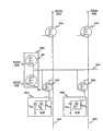
Fig. 2 is the diagram of TFT and the edge electronics that is used for the pixel in the addressing LCD.
Fig. 3 A is to use the diagram according to the LCD of the nano-wire transistor of the embodiment of the invention.
Fig. 3 B is the diagram according to the detailed part of the use nano-wire transistor LCD of the embodiment of the invention.
Fig. 4 is the diagram according to 4 nanowire pixel transistor in LCD of the embodiment of the invention.
Fig. 5 is the diagram according to a pair of nanowire row transistor in LCD of the embodiment of the invention.
Fig. 6 is the diagram according to two nanowire column transistor within LCD of the embodiment of the invention.
Embodiment
Should be appreciated that described concrete realization is an example of the present invention here, and do not represent to be confined to any other limitation scope of the present invention.In fact, for briefly, traditional electronic equipment, manufacturing, semiconductor equipment, nanotube, nanometer rods, nano wire and nano belt technology, and other function aspects of system's (and parts of the parts that work alone of system) can be in this detailed description.In addition,, do not represent to realize to be confined to this, can also use large-scale number of nanowires and spacing although be that the concrete realization of being discussed is provided with the quantity of nano wire and the spacing of these nano wires.In addition, can change the size and the formation of nano wire.Described realization does not indicate to limit to, and can use large-scale size and parts.
So use in the place, and term " nano wire " is often referred to any conductor of prolongation or partly leads material, and it comprises at least one cross sectional dimensions less than 500nm; And preferably less than 100nm; And has length-width ratio greater than 10 (length: width), be preferably greater than 50, and more preferably greater than 100.The example of this nano wire comprise similar below described semiconductor nanowires: the conductor or the semiconductor structure of other prolongation of disclosed international patent application No.WO 02/17362, WO 02/48701 and WO01/03208, CNT and similar size.
Although described here LCD model mainly based on the character that is associated with silicon, can use other type of nano wire, comprise semiconductor nanowires, it comprises and is selected from following semi-conducting material, for example, Si, Ge, Sn, Se; Te, B, C (comprising diamond), P, B-C, B-P (BP6), B-Si, Si-C, Si-Ge; Si-Sn and Ge-Sn, SiC, BN/BP/BAs, AlN/AlP/AlAs/AlSb, GaN/GaP/GaAs/GaSb, InN/InP/InAs/InSb, BN/BP/BAs, AlN/AlP/AlAs/AlSb, GaN/GaP/GaAs/GaSb; InN/InP/InAs/InSb, ZnO/ZnS/ZnSe/ZnTe, CdS/CdSe/CdTe, HgS/HgSe/HgTe, BeS/BeSe/BeTe/MgS/MgSe, GeS, GeSe, GeTe; SnS, SnSe, SnTe, PbO, PbS, PbSe, PbTe, CuF; CuCl, CuBr, CuI, AgF, AgCl, AgBr, AgI, BeSiN
2, CaCN
2, ZnGeP
2, CdSnAs
2, ZnSnSb
2, CuGeP
3, CuSi
2P
3, (Cu, and Ag) (Al, Ga, In, Tl, Fe) (S, Se, Te)
2, Si
3N
4, Ge
3N
4, Al
2O
3, (Al, Ga, In)
2(S, Se, Te)
3, Al
2CO, and two or more this semi-conductive appropriate combination.
In particular aspects, semiconductor can comprise dopant, and it is from the crowd who comprises following content: from the p type dopant of the group III of the periodic table of elements; N type dopant from the group V of the periodic table of elements; Be selected from the p type dopant of the group that comprises P, Al and In; Be selected from the n type dopant of the group that comprises P, As and Sb; P type dopant from the group II of the periodic table of elements; Be selected from the p type dopant of the group that comprises Mg, Zn, Cd and Hg; P type dopant from the group IV of the periodic table of elements; Be selected from the p type dopant of the group that comprises C and Si; Perhaps be selected from the n type dopant of the group that comprises Si, Ge, Sn, S, Se and Te.Those of ordinary skill in the art is readily appreciated that and can uses other known semiconductor dopant.
In addition, nano wire can comprise CNT, perhaps conductor or Semiconductor Organic polymeric material (for example, pentacene and transition metal oxide).
Therefore, although from demonstration purpose, the explanation that runs through here is called term " nano wire ", and its expression description here also comprises the use of nanotube.Nanotube can be formed at the described combination/film that is used for nanotube separately or combines with nanotube here, thereby described here characteristics and advantage are provided.In addition, nanotube need not comprise pure carbon, but can comprise for example other material such as boron, as what recognize through one of technology of the present invention.
In addition, the film of noticing that the film of nano wire of the present invention can be " foreign peoples (heterogeneous) ", it comprises: semiconductor nanowires and/or nanotube, and/or the combination of different nano wires, and/or any combination and/or the architectural characteristic of different parts.For example, " heterogeneous film " can comprise the nanowires/nanotubes with different-diameter and length, and nanotube and/or " heterogeneous structure " nanotube have different characteristic.
The longitudinal axis that means the most of nano wires in a group or a group nano wire through " aligning " in fact or " directed " is oriented within 30 degree of single direction.Although can think to surpass the i.e. great majority of a large amount of nano wires of 50%, in various embodiment, can think 60%, 75%, 80%, 90% or other percentage of nano wire be so directed great majority.Specific preferred aspect, the great majority of nano wire are oriented in 10 degree of institute's desired directions.In additional embodiment, the great majority of nano wire can be oriented in other scope number of institute's desired directions, comprise at random or isotropically directed.
The space that should be appreciated that here to be carried out (is for example described; " more than ", " following ", " top ", " below ", " top ", " bottom " etc.) only be used for purpose of description, and equipment of the present invention can carry out spatial arrangements with any direction or mode.
At last; In the example display type of concentrated discussion LCD; The present invention is applied to have any kind that uses electronic equipment to drive the display technology of the base plate that pixel changes, and includes but not limited to OLED, nanotube field effect display, plasma scope, micro-reflector display, micro electronmechanical (MEMs) display, electrochromic display device (ECD) of Organic Light Emitting Diode (OLED) display, dopen Nano crystal or the like.
Fig. 3 A provides the LCD300 that uses nano-wire transistor according to an embodiment of the invention.LCD 300 comprise one group of nanowire column transistor 310A to 310n, one group of nanowire row transistor to 320A to 320n, one group of nanowire pixel transistor 330A to 330z, one group of conductive column traces 340A to 340z, one group of row line 350A to 350n and one group of pixel 360A to 360z.Each nanowire column transistor is connected with one group of nanowire pixel transistor of edge from the row line of nanowire column transistor extension.For example, nanowire column transistor 310A is connected with nanowire pixel transistor 330A, 330M and 330S along row line 340A.Each nanowire row transistor pair is connected with one group of nanowire pixel transistor along the capable line that extends from nanowire row transistor.For example, nanowire row transistor 320A is connected with the one group of nanowire pixel transistor that follows line 350A.Nanowire pixel transistor is associated with corresponding pixel.For example, nanowire pixel transistor 330A is associated with pixel 360A.
In addition, nanowire edge electronics (not shown in Fig. 3 A) can be used to control nanometer alignment, row and pixel transistor.Nanowire edge electronics can also be used to drive row, row and the pixel transistor that present use nano wire is made.Nanowire edge electronics can comprise nanowire shift register, nanowire level shifter and nanowire buffer.Nanowire shift register refers to use the shift register of nano-wire transistor realization.Nanowire level shifter refers to use the level shifter of nano-wire transistor realization.Nanowire buffer refers to use the buffer of nanowire shifters realization.Can use nano-transistor to realize other type of edge electronics.
In operation, in the time will changing the brightness of pixel, apply voltage to the nanowire column transistor that is used for pixel place row.Conducting is used for the nanowire row transistor that pixel is expert at, thereby allows the current direction nanowire pixel transistor.When the nanowire pixel conducting, electric current flows through nanowire pixel transistor, thereby makes and have voltage at these pixel two ends, and it approximates greatly and puts on the voltage that lists with the hope light intensity that produces the transmission pixel.
Although Fig. 3 A shows wherein and is listed as, go and pixel transistor all is the embodiment of nano-wire transistor.In optional embodiment, the transistorized combination in any of nano-wire transistor and a-Si or poly-Si can be used for row, row and pixel transistor.For example, in one embodiment, pixel transistor can be a-Si TFT or poly-Si TFT, and the row and column transistor can be a nano-wire transistor.This is useful replacement, because relatively low for the performance requirement of pixel transistor, and can easily realize through a-Si TFT.In another example, rowed transistor can be a-Si TFT or poly-Si TFT, and the row and pixel transistor can be nano-wire transistor.In another example, row transistor can be a-Si TFT or poly-Si TFT, and row and pixel transistor can be nano-wire transistors.In another example, pixel transistor and row transistor can be a-Si TFT or poly-Si TFT, and rowed transistor can be a nano-wire transistor.In another example, pixel transistor and rowed transistor can be a-Si TFT or poly-Si TFT, and row transistor can be a nano-wire transistor.
Fig. 3 B provides the more detailed view according to the part 390 of the LCD300 of the embodiment of the invention.Fig. 3 B has stressed to use many aspects of the LCD of nano-wire transistor, that is, a pair of nanowire row transistor is connected to each row line, and each pixel has resistance and the electric capacity that is associated with it, and its influence is considered for transistorized design.Should be noted that the row and column line also has resistance and the electric capacity that is associated with it, influence design criterion.Nanowire row transistor 322 and 324 forms nanowire row transistor to 320A, and is connected with 330B with nanowire pixel transistor 330A through row line 350A.As the more detailed description according to following Fig. 5, nanowire row transistor 322 and 324 is used for conducting and ends nanowire pixel transistor, for example nanowire pixel transistor 330A and 330B.
In addition, Fig. 3 B has described each pixel and has had electric capacity and the resistance that is associated with this pixel.For example, pixel 360A comprises capacitor C
Lcd, capacitor C
sAnd resistance R
LcdCapacitor C
LcdExpression and the interior related electric capacity of liquid crystalline phase of pixel 360A.Resistance R
LcdExpression and the interior related resistance of liquid crystalline phase of pixel 360A.Capacitor C
sBe storage capacitance, add it so that improve performance.
According to the teaching here, those skilled in the relevant art can add nano-wire transistor among the LCD, and do not need a large amount of experiments.In addition, although design tool shows the use for the particular type of nano-wire transistor, example also is not intended to limit.Suitable those skilled in the relevant art can use employed notion in teaching and the following design tool of discussing here; Thereby utilize the nanowire semiconductor have variation characteristic on a large scale to develop integrated LCD or other type of display, these variation characteristics are type, dopant, the quantity and the orientation of line of nano crystal material for example.
The inventor has developed nano wire LCD design tool, so that the feasibility of nano-wire transistor is used in explanation to the electronic equipment of the liquid crystal in the pixel that drives LCD.Instrument comprises user interface, LCD design input block, nanowire characteristics input block, transistor requirements engine and nano wire design engine.User interface makes the user can import design criterion and display result.The collection of LCD design input block is about the information (for example LCD size, PEL density etc.) of LCD type.The nanowire characteristics input block is gathered the information about nanowire characteristics, comprises size, nano wire crystalline material, dopant and relevant performance characteristics.Transistor requirements engine produces row, row and the required performance requirement of pixel transistor.The output of nano wire design engine receiving crystal pipe requirements engine is as input, and definite concrete type of using required nano-wire transistor.
Nano wire LCD design tool is used to explain that nano-wire transistor can be used to drive the pixel within the LCD.The use of instrument also helps discerning and the unique benefit of in LCD, using nano-wire transistor to be associated.
In analysis, used conservative estimation for nanowire properties.Particularly, utilized the surface mobility (surface mobility) (μ s) of the only about half of representative value of piece silicon,, used suitable standard (μ s) wherein with respect to the dopant dose of the minimizing that is used for the migration relevant with dopant.In the raceway groove of the conductance of grid oxide-semiconductor control transistors, suppose that dopant is Na=10 therein
17/ cm
3, and in not having grid-controlled source electrode and draining, Nd=10
19/ cm
3Each all is assumed to be 10 μ m the length of raceway groove, source electrode and drain electrode.These hypothesis are guarded, so that guarantee to use the lithographic printing of least cost.
In addition, suppose to use the grid of annular, it means that gate contacts centers on nano wire.In addition, suppose that nano wire has nucleocapsid (core shell) design, silicon dioxide is centered around around the nanowire core and grid is coated in around the oxide.Make in this way, suppose that diameter is that the silicon nuclear nano wire of 60nm has the thick SiO of 40nm
2Shell makes nano wire have the overall diameter of 140nm.At last, suppose conservative threshold value and driving voltage, make threshold voltage (V
t) be assumed to be 2 volts and driving voltage (V
d) be assumed to be 5 volts.It is higher usually to be used for the transistorized driving voltage of a-Si and poly-Si.Employed voltage is more consistent in employed voltage hypothesis and the typical integrated circuit.The U.S. Provisional Application No.60/414 that on September 30th, 2002 submitted to, the No.60/468 that on May 7th, 323 and 2003 submitted to, 276 have described nanowire semiconductor and the performance data of supporting these hypothesis are provided, through in this reference its integral body being comprised.Attention can be made similar backplane electronics, and does not need conformal (conformal) grid and/or conformal gate oxide.
The hypothesis of LCD plate is based on the characteristic feature of existing LCD plate.Particularly, suppose that the LCD plate has 21 inches diagonal display, its resolution is 1024 * 768RGB pixel, refreshing frequency 60Hz.For each RGB pixel, there are three kinds of pixels (red, green and blue).Therefore, column pitch can be about 110 μ m and line space can be about 330 μ m.The electric capacity of supposing a pF is associated with each pixel.Suppose that the row line is the aluminium (Al) that 10 μ m are wide and 1 μ m is thick.Suppose to use above the thick SiO of 0.5 μ m
2Make the row insulating barrier.Suppose that the row line also is the aluminium (Al) that 10 μ m are wide and 2 μ m are thick.Suppose to use above the thick SiO of 2 μ m
2Make the row insulating barrier.The resistance and the electric capacity of line have been confirmed for the parameters of choice of row and column line.Otherwise, confirmed along the resistance of the line of pixel and electric capacity and transistor capacitance and resistance how soon the line that can switch has, and be expert at, need what performance rate in row and the pixel transistor.
According to these LCD criterions, the output of the instrument of manufacturing is used to row, row and pixel transistor definition demand.Those skilled in the relevant art it will be appreciated that the method for regulation TFT transistor size.See that for example people such as Satoru Tomita was published in the article Transistor Sizing for AMLCD Integrated TFT Drive Circuits of Journal of the Society of Information Display 339-404 page or leaf on April 5th, 1997.Particularly, for pixel transistor,, and need be used for pixel transistor greater than the off-resistances of 835G ohm with the model of the determined conducting resistance of needs less than 1.6M ohm.Conducting and dielectric resistance are based on multiple factor.Particularly, thus need highly to avoid the undesirable flicker effect in pixel by impedance.For fear of flickering, the capacitance voltage at pixel two ends must descend (coast) and not obviously leakage at the 16.6ms that refreshes between (refreshing frequency of supposing 60Hz).Leak rate is the function of the off-resistances of nanowire pixel transistor.Leakage in LCD resistance or the transistor will cause that the voltage on the pixel changes between refreshing, it can comprise undesirable flickering in the pixel.For the purpose of analyzing, suppose that the voltage on the pixel can not surpass 10% change between refreshing.On the other hand, require conducting resistance enough low, so that allow pixel in the available time, to charge.Consider that these criterions have obtained above-mentioned conducting and off-resistances.
In case these resistance are known, can confirm the quantity of required transistorized nano wire.To hypothesis its instrument of confirming has been used and to have had few nanowire pixel transistor that can satisfy design limit to 1 nano wire.Surpassing a nano wire also can accept.
Fig. 4 provides the diagram of 4 nanowire pixel transistor among the LCD according to an embodiment of the invention.Advise that as analysis result diagram has been described the use of wire nanowire pixel transistors.The part of shown LCD comprises 4 wire nanowire pixel transistors 410A, 410B, 410C and 410D; The part of a plurality of pixels comprises green pixel 420; Row line 430 and row line 440.Nanowire pixel transistor 410C has an end that is connected to transparent conductor, the tin indium oxide that for example is associated with green pixel 420.Indium tin oxide conductor is used for applying voltage to a side of liquid crystal cells.The other end of nanowire pixel transistor is connected on the row line 440.Between these tie points a bit on, nanowire pixel transistor 410C is connected to capable line 430.This tie point is as the grid of nanowire pixel transistor 410C.The voltage that the substrate notion is to be applied to capable line 430 is with conducting with by nanowire pixel transistor 410C.In optional embodiment, can in nanowire pixel transistor, use nano wire more than one.
In addition, analyze the design result that has also produced to nanowire row transistor, it has been explained and has used the feasibility of nano-wire transistor as row transistor.The use of instrument has been confirmed can satisfy with the nano-wire transistor that comprises at least 150 nano wires for the current design requirement of row transistor.Another problem of being considered is whether a pair of nanowire row transistor of inspection is suitable between two capable lines.The right size of Model Calculation explanation nanowire row transistor is significantly less than the distance (approximately less than 4-10%) between the capable line, so nano-wire transistor can easily be positioned between the capable line.
In optional embodiment, can use the nano wire of high mobility, so each transistor needs nano wire still less.In addition, these numerals will increase and decrease according to desirable pixel size.
Fig. 5 provides the diagram of a pair of nanowire row transistor in LCD.Diagram comprises nanowire row transistor 510, nanowire row transistor 520, pixel 530, nanowire pixel transistor 540, row line 550, row line 560, goes up line 570, gate trace 572, following line 574 and gate trace 576.Nanowire row transistor 510 comprises set of nanowires 515.Similarly, nanowire row transistor 520 comprises set of nanowires 525.Nanowire row transistor 510 and 520 is used for conducting and ends nanowire pixel transistor 540.
Nanowire row transistor 510 has a side of the set of nanowires 515 that links to each other with row line 560, and the opposite side that links to each other with last line 570.Last line 570 is connected on the conducting voltage.Point on each nano wire between these connections of concentrating on the set of nanowires 515 of serving as transistor gate is connected with gate trace 572.
Nanowire row transistor 520 has a side of the set of nanowires 525 that links to each other with row line 560, and the opposite side that links to each other with following line 574.Following line 574 ground connection.Point on each nano wire between these connections of concentrating on the set of nanowires 525 of serving as transistor gate is connected to gate trace 576.
When wanting conducting nanowire pixel 560, thereby apply grid voltage conducting nanowire row transistor 510 to gate trace 572.Simultaneously thereby gate trace 576 ground connection are ended nanowire row transistor 520.The result is, grid voltage is connected to nanowire pixel grid 545, thus conducting nanowire pixel 540.In the time nanowire pixel 510 will being ended, carry out opposite process.Remove grid voltage from gate trace 572, thereby by nanowire row transistor 510.And, apply grid voltage to gate trace 576 simultaneously, thus conducting nanowire row transistor 520.The result is, thereby the grid voltage of nanowire pixel transistor grid 545 becomes earthed voltage by nanowire pixel transistor 540.
In addition, analyze the design result that has also produced to nanowire column transistor, it has been explained and has used the feasibility of nano-wire transistor as rowed transistor.The use of instrument has confirmed that current design requirement can satisfy with the nano-wire transistor that comprises 3000 nano wires at least.Rowed transistor needs more nano wire than transistorized other type, thereby because require rowed transistor to have lower conducting resistance because it has the short charging interval, and alignment has a large amount of electric capacity.As under the situation of nanowire row transistor, instrument has explained that nano-wire transistor will be suitable between the row line.Under each situation, the concrete quantity that requires to satisfy the nano wire of performance criteria will receive the influence of nano crystal material type as discussed above, dopant magnitude and other factors.
Fig. 6 provides the diagram of two nanowire column transistor in the LCD according to an embodiment of the invention.Diagram comprises nanowire column transistor 610, nanowire column transistor 620, row line 630, video trace 640 and gate trace 650.Nanowire column transistor 610 comprises set of nanowires 615.Nanowire column transistor 610 can be used for applying voltage to the nanowire pixel transistor that is connected to row line 630.
Nanowire column transistor 610 has a side of the set of nanowires 615 that is connected with row line 630, and the opposite side that is connected with video trace 640.Video trace 640 is connected to the high pressure that is used to drive the nanowire pixel transistor that is connected with row line 630.This video voltage is provided with pixel voltage and therefore the brightness of pixel is set.Be connected to gate trace 650 as the point on each nano wire between these connections on the set of nanowires 615 of transistor gate jointly.Gate trace 650 is connected to the control circuit that is used for conducting and ends pixel column.
As can be viewed from Fig. 3 A, 3B, 4,5 and 6, can place nano wire by a direction.That is, in this case, all nano wires all are levels, and it is easier to make when the placement ratio nano line of the nano wire on substrate is multiple direction.The U.S. Provisional Application No.60/414 that submits on September 30th, 2002 has described the method that realizes the type location in 323.In addition, nano wire can be positioned over other direction according to concrete design criterion.In addition, be used to form pixel, the transistorized number of nanowires of row and column is the function of design criterion, can be including, but not limited to surpassing 2 nano wires, surpass 10 nano wires, surpass 100 nano wires and surpassing 1000 nano wires.
In addition, use the display of nano-wire transistor can be formed on the infrabasal plate with wide range of characteristics, for example lower glass substrate 180.Particularly, being used for the material of infrabasal plate can be including, but not limited to glass, plastics, polymer, crystal, metal or paper.In addition, be used for infrabasal plate material behavior can including, but not limited to be transparent material, trnaslucent materials, opaque material, color material, to the material of incident ray polarization and not to the material of incident ray polarization.At last, the material that is used for infrabasal plate can be " low temperature " material, and it has can be including, but not limited to the fusion temperature that is lower than 500 degrees Fahrenheits, is lower than 300 degrees Fahrenheits, is lower than 200 degrees Fahrenheits and is lower than 100 degrees Fahrenheits.
Conclusion
Provided exemplary embodiments of the present invention.The present invention is not limited to these examples.What propose these examples here is in order to describe rather than to limit.According to the teaching that is comprised here, possibility (comprise the content of describing here equivalent, expansion, variant, depart from etc.) be readily appreciated that for those those skilled in the relevant art.This possibility is within scope of the present invention and essence.
Claims (45)
1. active matrix base plate that in display, uses comprises:
A plurality of pixels;
A plurality of rowed transistors, the rowed transistor within wherein said a plurality of rowed transistors applies voltage to the subclass two ends of a plurality of pixel transistors; With
A plurality of row transistors, at least two row transistor conductings within wherein said a plurality of row transistors or by corresponding pixel transistor;
A plurality of pixel transistors; Wherein be controlled at the corresponding pixel within said a plurality of pixel at the pixel transistor within said a plurality of pixel transistors; Each rowed transistor within each pixel transistor within wherein said a plurality of pixel transistor, the said a plurality of rowed transistors and each row transistor within said a plurality of row transistor are nano-wire transistors; Said nano-wire transistor is included in a plurality of nano wires that extend between transistorized source electrode and the drain electrode, and each nano-wire transistor comprises enough at least to hope that the speed pixels is charged and the nano wire of the average number of discharging; And
Edge electronics; It controls in said rowed transistor, said row transistor and the said pixel transistor one or more; Wherein said edge electronics comprises a plurality of nano-wire transistors, and each nano-wire transistor is included in a plurality of nano wires that extend between this transistorized first source electrode and first drain electrode.
2. active matrix base plate according to claim 1 is characterized in that each row nano-wire transistor comprises at least 100 nano wires that between source electrode and drain electrode, extend at least.
3. active matrix base plate according to claim 1 is characterized in that each row nano-wire transistor comprises at least 100 nano wires that between source electrode and drain electrode, extend at least.
4. active matrix base plate according to claim 1 is characterized in that nanowire edge electronics comprises nanowire buffer.
5. active matrix base plate according to claim 1 is characterized in that nanowire edge electronics comprises nanowire shift register.
6. active matrix base plate according to claim 1 is characterized in that nanowire edge electronics comprises nanowire level shifter.
7. active matrix base plate according to claim 1 is characterized in that display is a LCD.
8. active matrix base plate according to claim 1 is characterized in that display is OLED OLED.
9. active matrix base plate according to claim 8 is characterized in that said OLED comprises nanocrystal.
10. active matrix base plate according to claim 1 is characterized in that display is an electrophoretic display device (EPD).
11. active matrix base plate according to claim 1 is characterized in that display is a plasma scope.
12. active matrix base plate according to claim 1 is characterized in that display is an electrochromic display device (ECD).
13. active matrix base plate according to claim 1 is characterized in that display is micro electronmechanical MEMs display.
14. active matrix base plate according to claim 1 is characterized in that display is the micro-reflector display.
15. active matrix base plate according to claim 1 is characterized in that display is a Field Emission Display.
16. active matrix base plate according to claim 15 is characterized in that display is the nanotube field emission display.
17. active matrix base plate according to claim 1 is characterized in that display is a rigidity.
18. active matrix base plate according to claim 1 is characterized in that display is flexible.
19. active matrix base plate according to claim 1 is characterized in that display is an on-plane surface.
20. active matrix base plate according to claim 1 is characterized in that said nano wire has nucleocapsid design, wherein silicon dioxide growth around nanowire core and grid be coated in around the oxide.
21. active matrix base plate according to claim 20 is characterized in that said nano wire also comprises the gate contacts around said nano wire.
22. the LCD with infrabasal plate comprises:
(a) a plurality of pixels;
(b) a plurality of pixel transistors, the pixel transistor within wherein said a plurality of pixel transistors is controlled the corresponding pixel within said a plurality of pixel;
(c) a plurality of rowed transistors, the rowed transistor within wherein said a plurality of rowed transistors applies voltage to the subclass two ends of said a plurality of pixel transistors; And
(d) a plurality of row transistors; At least two row transistor conductings within wherein said a plurality of row transistor and by corresponding pixel transistor; I wherein) said a plurality of pixel transistors, ii) in said a plurality of rowed transistor and the iii) said a plurality of row transistors be nano-wire transistor one of at least; Said nano-wire transistor is included in a plurality of nano wires that extend between source electrode and the drain electrode of said nano-wire transistor, and each nano-wire transistor comprises enough at least to hope that the speed pixels is charged and the nano wire of the average number of discharging; And
(e) edge electronics; It controls in said rowed transistor, said row transistor and the said pixel transistor one or more; Wherein said edge electronics comprises a plurality of nano-wire transistors, and each nano-wire transistor is included in a plurality of nano wires that extend between this transistorized first source electrode and first drain electrode.
23. LCD according to claim 22 is characterized in that nanowire edge electronics comprises nanowire buffer.
24. LCD according to claim 22 is characterized in that nanowire edge electronics comprises nanowire shift register.
25. LCD according to claim 22 is characterized in that nanowire edge electronics comprises nanowire level shifter.
26. LCD according to claim 22 is characterized in that pixel transistor, the rowed transistor within said a plurality of rowed transistors and the row transistor within said a plurality of row transistor within said a plurality of pixel transistor is nano-wire transistor.
27. LCD according to claim 22 is characterized in that i) said a plurality of pixel transistors, ii) in said a plurality of rowed transistor and the iii) said a plurality of row transistors be the a-Si thin-film transistor one of at least.
28. LCD according to claim 22 is characterized in that i) said a plurality of pixel transistors, ii) in said a plurality of rowed transistor and the iii) said a plurality of row transistors be body Si thin-film transistor one of at least.
29. LCD according to claim 22 is characterized in that i) said a plurality of pixel transistors, ii) in said a plurality of rowed transistor and the iii) said a plurality of row transistors be organic semiconductor one of at least.
30. LCD according to claim 22 is characterized in that i) said a plurality of pixel transistors, ii) in said a plurality of rowed transistor and the iii) said a plurality of row transistors be polycrystalline SiTFT one of at least.
31. according to the LCD of claim 22, it is characterized in that being used to form transistorized nano wire is the parallel lines of aiming at.
32., it is characterized in that at random and zener rice noodles isotropically according to the LCD of claim 22.
33. LCD according to claim 22 is characterized in that nanowire column transistor is between the row line.
34. LCD according to claim 22 is characterized in that nanowire column transistor is positioned at and row line conllinear place.
35. LCD according to claim 22 is characterized in that nanowire row transistor is between the row line.
36. LCD according to claim 22 is characterized in that nanowire row transistor is positioned at and row line conllinear place.
37. LCD according to claim 22 is characterized in that nano-wire transistor comprises the source electrode that connects nano-wire transistor and at least 10 nano wires of drain electrode.
38. LCD according to claim 22 is characterized in that nano-wire transistor comprises the source electrode that connects nano-wire transistor and at least 100 nano wires of drain electrode.
39. LCD according to claim 22 is characterized in that infrabasal plate is a flexible material.
40. LCD according to claim 22 is characterized in that infrabasal plate is to have the cryogenic material that fusion temperature is lower than 500 degrees Fahrenheits.
41. LCD according to claim 22 is characterized in that infrabasal plate is plastics.
42. LCD according to claim 22 is characterized in that infrabasal plate is translucent material.
43. LCD according to claim 22 is characterized in that said nano wire comprises nucleocapsid design, wherein silicon dioxide growth around nanowire core and grid be coated in around the oxide.
44. an employed active matrix base plate in display comprises:
A plurality of pixels;
A plurality of amorphous silicon pixel transistors, the pixel transistor within wherein said a plurality of pixel transistors is controlled at the corresponding pixel within said a plurality of pixel;
A plurality of row transistors are configured to make electric current can flow to said pixel transistor; And
A plurality of rowed transistors; Rowed transistor within wherein said a plurality of rowed transistor applies voltage to the subclass two ends of said a plurality of pixel transistors; And each rowed transistor within wherein said a plurality of pixel transistor is a nano-wire transistor; Said nano-wire transistor is included in a plurality of nano wires that extend between transistorized source electrode and the drain electrode, and each nano-wire transistor comprises enough at least to hope that the speed pixels is charged and the nano wire of the average number of discharging; And
Edge electronics; It controls in said rowed transistor, said row transistor and the said pixel transistor one or more; Wherein said edge electronics comprises a plurality of nano-wire transistors, and each nano-wire transistor is included in a plurality of nano wires that extend between this transistorized first source electrode and first drain electrode.
45., it is characterized in that each nano-wire transistor comprises at least 100 nano wires that between source electrode and drain electrode, extend at least according to the described active matrix base plate of claim 44.
Applications Claiming Priority (8)
| Application Number | Priority Date | Filing Date | Title |
|---|---|---|---|
| US41432302P | 2002-09-30 | 2002-09-30 | |
| US41435902P | 2002-09-30 | 2002-09-30 | |
| US60/414,359 | 2002-09-30 | ||
| US60/414,323 | 2002-09-30 | ||
| US46827603P | 2003-05-07 | 2003-05-07 | |
| US60/468,276 | 2003-05-07 | ||
| US48880103P | 2003-07-22 | 2003-07-22 | |
| US60/488,801 | 2003-07-22 |
Related Parent Applications (1)
| Application Number | Title | Priority Date | Filing Date |
|---|---|---|---|
| CN 03825281 Division CN1703730A (en) | 2002-09-30 | 2003-09-30 | Integrated displays using nanowire transistors |
Publications (1)
| Publication Number | Publication Date |
|---|---|
| CN102569349A true CN102569349A (en) | 2012-07-11 |
Family
ID=32074643
Family Applications (1)
| Application Number | Title | Priority Date | Filing Date |
|---|---|---|---|
| CN201210040611XA Pending CN102569349A (en) | 2002-09-30 | 2003-09-30 | Integrated displays using nanowire transistors |
Country Status (8)
| Country | Link |
|---|---|
| US (2) | US7102605B2 (en) |
| EP (1) | EP1563480A4 (en) |
| JP (1) | JP4669784B2 (en) |
| KR (1) | KR101043578B1 (en) |
| CN (1) | CN102569349A (en) |
| CA (1) | CA2499944A1 (en) |
| TW (1) | TWI354261B (en) |
| WO (1) | WO2004032190A2 (en) |
Families Citing this family (129)
| Publication number | Priority date | Publication date | Assignee | Title |
|---|---|---|---|---|
| US20110125412A1 (en) * | 1998-12-17 | 2011-05-26 | Hach Company | Remote monitoring of carbon nanotube sensor |
| US9056783B2 (en) * | 1998-12-17 | 2015-06-16 | Hach Company | System for monitoring discharges into a waste water collection system |
| US7454295B2 (en) | 1998-12-17 | 2008-11-18 | The Watereye Corporation | Anti-terrorism water quality monitoring system |
| US8958917B2 (en) * | 1998-12-17 | 2015-02-17 | Hach Company | Method and system for remote monitoring of fluid quality and treatment |
| KR100862131B1 (en) | 2000-08-22 | 2008-10-09 | 프레지던트 앤드 펠로우즈 오브 하버드 칼리지 | Semiconductor nanowires manufacturing method |
| AU2904602A (en) | 2000-12-11 | 2002-06-24 | Harvard College | Nanosensors |
| US7417782B2 (en) | 2005-02-23 | 2008-08-26 | Pixtronix, Incorporated | Methods and apparatus for spatial light modulation |
| US8920619B2 (en) | 2003-03-19 | 2014-12-30 | Hach Company | Carbon nanotube sensor |
| US7397455B2 (en) * | 2003-06-06 | 2008-07-08 | Samsung Electronics Co., Ltd. | Liquid crystal display backplane layouts and addressing for non-standard subpixel arrangements |
| GB0323285D0 (en) * | 2003-10-04 | 2003-11-05 | Koninkl Philips Electronics Nv | Device and method of making a device having a patterned layer on a flexible substrate |
| US20110039690A1 (en) * | 2004-02-02 | 2011-02-17 | Nanosys, Inc. | Porous substrates, articles, systems and compositions comprising nanofibers and methods of their use and production |
| US8025960B2 (en) * | 2004-02-02 | 2011-09-27 | Nanosys, Inc. | Porous substrates, articles, systems and compositions comprising nanofibers and methods of their use and production |
| US7553371B2 (en) * | 2004-02-02 | 2009-06-30 | Nanosys, Inc. | Porous substrates, articles, systems and compositions comprising nanofibers and methods of their use and production |
| US7532194B2 (en) * | 2004-02-03 | 2009-05-12 | Idc, Llc | Driver voltage adjuster |
| KR100708644B1 (en) * | 2004-02-26 | 2007-04-17 | 삼성에스디아이 주식회사 | TFT, flat panel display device therewith, manufacturing method of TFT, manufacturing method of flat panel display, and manufacturing method of donor sheet |
| US6912082B1 (en) * | 2004-03-11 | 2005-06-28 | Palo Alto Research Center Incorporated | Integrated driver electronics for MEMS device using high voltage thin film transistors |
| US7057881B2 (en) * | 2004-03-18 | 2006-06-06 | Nanosys, Inc | Nanofiber surface based capacitors |
| US7195733B2 (en) | 2004-04-27 | 2007-03-27 | The Board Of Trustees Of The University Of Illinois | Composite patterning devices for soft lithography |
| CN102351169B (en) | 2004-04-30 | 2013-11-27 | 纳米系统公司 | Systems and methods for nanowire growth and harvesting |
| US20050279274A1 (en) * | 2004-04-30 | 2005-12-22 | Chunming Niu | Systems and methods for nanowire growth and manufacturing |
| US7785922B2 (en) | 2004-04-30 | 2010-08-31 | Nanosys, Inc. | Methods for oriented growth of nanowires on patterned substrates |
| US7521292B2 (en) | 2004-06-04 | 2009-04-21 | The Board Of Trustees Of The University Of Illinois | Stretchable form of single crystal silicon for high performance electronics on rubber substrates |
| US7557367B2 (en) | 2004-06-04 | 2009-07-07 | The Board Of Trustees Of The University Of Illinois | Stretchable semiconductor elements and stretchable electrical circuits |
| US8217381B2 (en) | 2004-06-04 | 2012-07-10 | The Board Of Trustees Of The University Of Illinois | Controlled buckling structures in semiconductor interconnects and nanomembranes for stretchable electronics |
| US7799699B2 (en) | 2004-06-04 | 2010-09-21 | The Board Of Trustees Of The University Of Illinois | Printable semiconductor structures and related methods of making and assembling |
| US7943491B2 (en) | 2004-06-04 | 2011-05-17 | The Board Of Trustees Of The University Of Illinois | Pattern transfer printing by kinetic control of adhesion to an elastomeric stamp |
| CA2572798A1 (en) | 2004-07-07 | 2006-07-27 | Nanosys, Inc. | Systems and methods for harvesting and integrating nanowires |
| US8558311B2 (en) | 2004-09-16 | 2013-10-15 | Nanosys, Inc. | Dielectrics using substantially longitudinally oriented insulated conductive wires |
| US8089152B2 (en) * | 2004-09-16 | 2012-01-03 | Nanosys, Inc. | Continuously variable graded artificial dielectrics using nanostructures |
| US7365395B2 (en) * | 2004-09-16 | 2008-04-29 | Nanosys, Inc. | Artificial dielectrics using nanostructures |
| CN101124638A (en) | 2004-12-06 | 2008-02-13 | 哈佛大学 | Nanoscale wire-based data storage |
| US7116275B2 (en) | 2005-01-28 | 2006-10-03 | Lockheed Martin Corporation | Operationally reconfigurable array |
| US9261694B2 (en) | 2005-02-23 | 2016-02-16 | Pixtronix, Inc. | Display apparatus and methods for manufacture thereof |
| US9229222B2 (en) | 2005-02-23 | 2016-01-05 | Pixtronix, Inc. | Alignment methods in fluid-filled MEMS displays |
| US7999994B2 (en) | 2005-02-23 | 2011-08-16 | Pixtronix, Inc. | Display apparatus and methods for manufacture thereof |
| US7755582B2 (en) | 2005-02-23 | 2010-07-13 | Pixtronix, Incorporated | Display methods and apparatus |
| US7675665B2 (en) | 2005-02-23 | 2010-03-09 | Pixtronix, Incorporated | Methods and apparatus for actuating displays |
| US9158106B2 (en) | 2005-02-23 | 2015-10-13 | Pixtronix, Inc. | Display methods and apparatus |
| US8159428B2 (en) | 2005-02-23 | 2012-04-17 | Pixtronix, Inc. | Display methods and apparatus |
| US9082353B2 (en) | 2010-01-05 | 2015-07-14 | Pixtronix, Inc. | Circuits for controlling display apparatus |
| US7271945B2 (en) * | 2005-02-23 | 2007-09-18 | Pixtronix, Inc. | Methods and apparatus for actuating displays |
| US7746529B2 (en) | 2005-02-23 | 2010-06-29 | Pixtronix, Inc. | MEMS display apparatus |
| US8310442B2 (en) | 2005-02-23 | 2012-11-13 | Pixtronix, Inc. | Circuits for controlling display apparatus |
| US8519945B2 (en) | 2006-01-06 | 2013-08-27 | Pixtronix, Inc. | Circuits for controlling display apparatus |
| US7742016B2 (en) | 2005-02-23 | 2010-06-22 | Pixtronix, Incorporated | Display methods and apparatus |
| US20070205969A1 (en) | 2005-02-23 | 2007-09-06 | Pixtronix, Incorporated | Direct-view MEMS display devices and methods for generating images thereon |
| US8482496B2 (en) | 2006-01-06 | 2013-07-09 | Pixtronix, Inc. | Circuits for controlling MEMS display apparatus on a transparent substrate |
| KR101109623B1 (en) * | 2005-04-07 | 2012-01-31 | 엘지디스플레이 주식회사 | TFT for display device and method of fabricating of the same |
| KR101145146B1 (en) | 2005-04-07 | 2012-05-14 | 엘지디스플레이 주식회사 | TFT and method of fabricating of the same |
| US20100227382A1 (en) | 2005-05-25 | 2010-09-09 | President And Fellows Of Harvard College | Nanoscale sensors |
| WO2006132659A2 (en) | 2005-06-06 | 2006-12-14 | President And Fellows Of Harvard College | Nanowire heterostructures |
| US7927948B2 (en) | 2005-07-20 | 2011-04-19 | Micron Technology, Inc. | Devices with nanocrystals and methods of formation |
| EP1750310A3 (en) * | 2005-08-03 | 2009-07-15 | Samsung Electro-Mechanics Co., Ltd. | Omni-directional reflector and light emitting diode adopting the same |
| US7575978B2 (en) | 2005-08-04 | 2009-08-18 | Micron Technology, Inc. | Method for making conductive nanoparticle charge storage element |
| US7989290B2 (en) | 2005-08-04 | 2011-08-02 | Micron Technology, Inc. | Methods for forming rhodium-based charge traps and apparatus including rhodium-based charge traps |
| US7692610B2 (en) * | 2005-11-30 | 2010-04-06 | Semiconductor Energy Laboratory Co., Ltd. | Display device |
| JP4500797B2 (en) * | 2005-12-06 | 2010-07-14 | キヤノン株式会社 | CIRCUIT DEVICE AND DISPLAY DEVICE HAVING CAPACITOR AND FIELD EFFECT TRANSISTOR |
| EP1796162A3 (en) | 2005-12-06 | 2010-06-02 | Canon Kabushiki Kaisha | Circuit element having capacitor and field effect transistor comprising nanowires |
| US7951422B2 (en) * | 2005-12-29 | 2011-05-31 | Nanosys, Inc. | Methods for oriented growth of nanowires on patterned substrates |
| US7741197B1 (en) | 2005-12-29 | 2010-06-22 | Nanosys, Inc. | Systems and methods for harvesting and reducing contamination in nanowires |
| US7427201B2 (en) * | 2006-01-12 | 2008-09-23 | Green Cloak Llc | Resonant frequency filtered arrays for discrete addressing of a matrix |
| US8526096B2 (en) | 2006-02-23 | 2013-09-03 | Pixtronix, Inc. | Mechanical light modulators with stressed beams |
| JP4970997B2 (en) | 2006-03-30 | 2012-07-11 | パナソニック株式会社 | Manufacturing method of nanowire transistor |
| JP5060740B2 (en) * | 2006-05-26 | 2012-10-31 | シャープ株式会社 | Integrated circuit device, method for manufacturing the same, and display device |
| US7876489B2 (en) | 2006-06-05 | 2011-01-25 | Pixtronix, Inc. | Display apparatus with optical cavities |
| JP2009540333A (en) | 2006-06-12 | 2009-11-19 | プレジデント アンド フェロウズ オブ ハーバード カレッジ | Nanosensors and related technologies |
| GB0611452D0 (en) * | 2006-06-12 | 2006-07-19 | Plastic Logic Ltd | Page refreshing e-reader |
| US7554621B2 (en) * | 2006-06-26 | 2009-06-30 | Panasonic Corporation | Nanostructured integrated circuits with capacitors |
| WO2008033303A2 (en) | 2006-09-11 | 2008-03-20 | President And Fellows Of Harvard College | Branched nanoscale wires |
| KR101545219B1 (en) * | 2006-10-12 | 2015-08-18 | 캄브리오스 테크놀로지즈 코포레이션 | Nanowire-based transparent conductors and applications thereof |
| EP2080045A1 (en) | 2006-10-20 | 2009-07-22 | Pixtronix Inc. | Light guides and backlight systems incorporating light redirectors at varying densities |
| CN101573778B (en) | 2006-11-07 | 2013-01-02 | 奈米系统股份有限公司 | Systems and methods for nanowire growth |
| US8575663B2 (en) | 2006-11-22 | 2013-11-05 | President And Fellows Of Harvard College | High-sensitivity nanoscale wire sensors |
| EP2104954B1 (en) | 2007-01-17 | 2022-03-16 | The Board of Trustees of the University of Illinois | Optical systems fabricated by printing-based assembly |
| US9176318B2 (en) | 2007-05-18 | 2015-11-03 | Pixtronix, Inc. | Methods for manufacturing fluid-filled MEMS displays |
| US7852546B2 (en) | 2007-10-19 | 2010-12-14 | Pixtronix, Inc. | Spacers for maintaining display apparatus alignment |
| WO2008097867A1 (en) * | 2007-02-07 | 2008-08-14 | Green Cloak Llc | Displays including addressable trace structures |
| US8183566B2 (en) * | 2007-03-01 | 2012-05-22 | Hewlett-Packard Development Company, L.P. | Hetero-crystalline semiconductor device and method of making same |
| US8367506B2 (en) | 2007-06-04 | 2013-02-05 | Micron Technology, Inc. | High-k dielectrics with gold nano-particles |
| KR100868941B1 (en) * | 2007-07-20 | 2008-11-17 | 황장환 | Oled using cnt without catalyst and method for fabricating the same |
| KR100868940B1 (en) * | 2007-07-20 | 2008-11-17 | 황장환 | Doped cnt oled and method for fabricating the same |
| US8035590B2 (en) * | 2007-11-02 | 2011-10-11 | Sony Corporation | Color liquid crystal display device assembly |
| US8273983B2 (en) * | 2007-12-21 | 2012-09-25 | Hewlett-Packard Development Company, L.P. | Photonic device and method of making same using nanowires |
| WO2009111641A1 (en) | 2008-03-05 | 2009-09-11 | The Board Of Trustees Of The University Of Illinois | Stretchable and foldable electronic devices |
| GB2459251A (en) | 2008-04-01 | 2009-10-21 | Sharp Kk | Semiconductor nanowire devices |
| US8248560B2 (en) | 2008-04-18 | 2012-08-21 | Pixtronix, Inc. | Light guides and backlight systems incorporating prismatic structures and light redirectors |
| WO2010005707A1 (en) | 2008-06-16 | 2010-01-14 | The Board Of Trustees Of The University Of Illinois | Medium scale carbon nanotube thin film integrated circuits on flexible plastic substrates |
| EP2304802B8 (en) * | 2008-07-18 | 2013-12-04 | Panasonic Corporation | Semiconductor material |
| US8886334B2 (en) | 2008-10-07 | 2014-11-11 | Mc10, Inc. | Systems, methods, and devices using stretchable or flexible electronics for medical applications |
| WO2010042653A1 (en) | 2008-10-07 | 2010-04-15 | Mc10, Inc. | Catheter balloon having stretchable integrated circuitry and sensor array |
| US8389862B2 (en) | 2008-10-07 | 2013-03-05 | Mc10, Inc. | Extremely stretchable electronics |
| JP5442234B2 (en) | 2008-10-24 | 2014-03-12 | 株式会社半導体エネルギー研究所 | Semiconductor device and display device |
| US8169679B2 (en) | 2008-10-27 | 2012-05-01 | Pixtronix, Inc. | MEMS anchors |
| US7884004B2 (en) * | 2009-02-04 | 2011-02-08 | International Business Machines Corporation | Maskless process for suspending and thinning nanowires |
| EP2430652B1 (en) | 2009-05-12 | 2019-11-20 | The Board of Trustees of the University of Illionis | Printed assemblies of ultrathin, microscale inorganic light emitting diodes for deformable and semitransparent displays |
| EP4068914A3 (en) | 2009-05-19 | 2022-10-12 | OneD Material, Inc. | Nanostructured materials for battery applications |
| US20120135158A1 (en) | 2009-05-26 | 2012-05-31 | Sharp Kabushiki Kaisha | Methods and systems for electric field deposition of nanowires and other devices |
| US8623288B1 (en) | 2009-06-29 | 2014-01-07 | Nanosys, Inc. | Apparatus and methods for high density nanowire growth |
| US9297796B2 (en) | 2009-09-24 | 2016-03-29 | President And Fellows Of Harvard College | Bent nanowires and related probing of species |
| US9723122B2 (en) | 2009-10-01 | 2017-08-01 | Mc10, Inc. | Protective cases with integrated electronics |
| US9936574B2 (en) | 2009-12-16 | 2018-04-03 | The Board Of Trustees Of The University Of Illinois | Waterproof stretchable optoelectronics |
| WO2011084450A1 (en) | 2009-12-16 | 2011-07-14 | The Board Of Trustees Of The University Of Illinois | Electrophysiology in-vivo using conformal electronics |
| US10441185B2 (en) | 2009-12-16 | 2019-10-15 | The Board Of Trustees Of The University Of Illinois | Flexible and stretchable electronic systems for epidermal electronics |
| CN104916258B (en) | 2010-02-02 | 2018-02-16 | 追踪有限公司 | For controlling the circuit of display device |
| CN102834763B (en) | 2010-02-02 | 2015-07-22 | 皮克斯特罗尼克斯公司 | Methods for manufacturing cold seal fluid-filled display apparatus |
| CN104224171B (en) | 2010-03-17 | 2017-06-09 | 伊利诺伊大学评议会 | Implantable bio-medical instrument based on biological absorbable matrix |
| WO2012097163A1 (en) | 2011-01-14 | 2012-07-19 | The Board Of Trustees Of The University Of Illinois | Optical component array having adjustable curvature |
| WO2012158709A1 (en) | 2011-05-16 | 2012-11-22 | The Board Of Trustees Of The University Of Illinois | Thermally managed led arrays assembled by printing |
| EP2712491B1 (en) | 2011-05-27 | 2019-12-04 | Mc10, Inc. | Flexible electronic structure |
| EP2713863B1 (en) | 2011-06-03 | 2020-01-15 | The Board of Trustees of the University of Illionis | Conformable actively multiplexed high-density surface electrode array for brain interfacing |
| WO2013089867A2 (en) | 2011-12-01 | 2013-06-20 | The Board Of Trustees Of The University Of Illinois | Transient devices designed to undergo programmable transformations |
| KR101963229B1 (en) | 2011-12-05 | 2019-03-29 | 삼성전자주식회사 | Folderble thin film transistor |
| CN105283122B (en) | 2012-03-30 | 2020-02-18 | 伊利诺伊大学评议会 | Appendage mountable electronic device conformable to a surface |
| US9786850B2 (en) | 2012-09-07 | 2017-10-10 | President And Fellows Of Harvard College | Methods and systems for scaffolds comprising nanoelectronic components |
| US9457128B2 (en) | 2012-09-07 | 2016-10-04 | President And Fellows Of Harvard College | Scaffolds comprising nanoelectronic components for cells, tissues, and other applications |
| US9171794B2 (en) | 2012-10-09 | 2015-10-27 | Mc10, Inc. | Embedding thin chips in polymer |
| US9134552B2 (en) | 2013-03-13 | 2015-09-15 | Pixtronix, Inc. | Display apparatus with narrow gap electrostatic actuators |
| US20160027846A1 (en) * | 2013-04-05 | 2016-01-28 | President And Fellow Of Harvard College | Three-dimensional networks comprising nanoelectronics |
| US9379166B2 (en) * | 2014-11-04 | 2016-06-28 | Atom Nanoelectronics, Inc. | Active matrix light emitting diodes display module with carbon nanotubes control circuits and methods of fabrication |
| JP2015181166A (en) * | 2015-04-14 | 2015-10-15 | 株式会社半導体エネルギー研究所 | display device |
| AU2016270807A1 (en) | 2015-06-01 | 2017-12-14 | The Board Of Trustees Of The University Of Illinois | Miniaturized electronic systems with wireless power and near-field communication capabilities |
| JP2018524566A (en) | 2015-06-01 | 2018-08-30 | ザ ボード オブ トラスティーズ オブ ザ ユニヴァーシティー オブ イリノイ | Alternative UV sensing method |
| US10925543B2 (en) | 2015-11-11 | 2021-02-23 | The Board Of Trustees Of The University Of Illinois | Bioresorbable silicon electronics for transient implants |
| CN105373259B (en) * | 2015-12-11 | 2018-11-27 | 上海中航光电子有限公司 | A kind of array substrate, display panel and display device |
| US10117305B2 (en) | 2016-05-09 | 2018-10-30 | Industrial Technology Research Institute | Driving system and method for planar organic electroluminescent device |
| CN111333103B (en) * | 2020-04-04 | 2022-03-15 | 南开大学 | Method for digitally and controllably printing IZO semiconductor nanowires |
| CN111393159A (en) * | 2020-04-04 | 2020-07-10 | 南开大学 | Method for digitally and controllably printing IZO nanowire electrode |
| CN114647119B (en) * | 2020-12-18 | 2023-10-13 | 京东方科技集团股份有限公司 | Dimming structure and dimming equipment |
| CN113140452A (en) * | 2021-04-21 | 2021-07-20 | 北海惠科光电技术有限公司 | Indium tin oxide nanowire, preparation method thereof and thin film transistor |
Family Cites Families (44)
| Publication number | Priority date | Publication date | Assignee | Title |
|---|---|---|---|---|
| JPS6392928A (en) * | 1986-10-07 | 1988-04-23 | Matsushita Electric Ind Co Ltd | Color liquid crystal display using active double matrix |
| JP2572003B2 (en) * | 1992-03-30 | 1997-01-16 | 三星電子株式会社 | Method of manufacturing thin film transistor having three-dimensional multi-channel structure |
| US5962863A (en) * | 1993-09-09 | 1999-10-05 | The United States Of America As Represented By The Secretary Of The Navy | Laterally disposed nanostructures of silicon on an insulating substrate |
| JP3476241B2 (en) * | 1994-02-25 | 2003-12-10 | 株式会社半導体エネルギー研究所 | Display method of active matrix type display device |
| US5747928A (en) * | 1994-10-07 | 1998-05-05 | Iowa State University Research Foundation, Inc. | Flexible panel display having thin film transistors driving polymer light-emitting diodes |
| WO1997049132A1 (en) * | 1996-06-20 | 1997-12-24 | Jeffrey Frey | Light-emitting semiconductor device |
| KR100518923B1 (en) * | 1997-10-31 | 2005-10-06 | 세이코 엡슨 가부시키가이샤 | Electro-optical device and electronic apparatus |
| DE69918308T2 (en) * | 1998-04-10 | 2004-10-21 | E Ink Corp | ELECTRONIC DISPLAY BASED ON ORGANIC FIELD EFFECT TRANSISTORS |
| US6140993A (en) * | 1998-06-16 | 2000-10-31 | Atmel Corporation | Circuit for transferring high voltage video signal without signal loss |
| US6459095B1 (en) * | 1999-03-29 | 2002-10-01 | Hewlett-Packard Company | Chemically synthesized and assembled electronics devices |
| US6256767B1 (en) * | 1999-03-29 | 2001-07-03 | Hewlett-Packard Company | Demultiplexer for a molecular wire crossbar network (MWCN DEMUX) |
| US6815218B1 (en) * | 1999-06-09 | 2004-11-09 | Massachusetts Institute Of Technology | Methods for manufacturing bioelectronic devices |
| EP2239794A3 (en) | 1999-07-02 | 2011-03-23 | President and Fellows of Harvard College | Nanoscopic wire-based devices, arrays, and methods of their manufacture |
| US6438025B1 (en) * | 1999-09-08 | 2002-08-20 | Sergei Skarupo | Magnetic memory device |
| RU2173003C2 (en) * | 1999-11-25 | 2001-08-27 | Септре Электроникс Лимитед | Method for producing silicon nanostructure, lattice of silicon quantum conducting tunnels, and devices built around them |
| KR100360476B1 (en) * | 2000-06-27 | 2002-11-08 | 삼성전자 주식회사 | Vertical nano-size transistor using carbon nanotubes and manufacturing method thereof |
| US6586785B2 (en) * | 2000-06-29 | 2003-07-01 | California Institute Of Technology | Aerosol silicon nanoparticles for use in semiconductor device fabrication |
| JP4112358B2 (en) * | 2000-07-04 | 2008-07-02 | インフィネオン テクノロジーズ アクチエンゲゼルシャフト | Field effect transistor |
| CN1251962C (en) * | 2000-07-18 | 2006-04-19 | Lg电子株式会社 | Method of horizontal growth of carbon nanotube and field effect transistor using carbon nanotube |
| DE10036897C1 (en) * | 2000-07-28 | 2002-01-03 | Infineon Technologies Ag | Field effect transistor used in a switching arrangement comprises a gate region between a source region and a drain region |
| US6447663B1 (en) * | 2000-08-01 | 2002-09-10 | Ut-Battelle, Llc | Programmable nanometer-scale electrolytic metal deposition and depletion |
| KR100862131B1 (en) | 2000-08-22 | 2008-10-09 | 프레지던트 앤드 펠로우즈 오브 하버드 칼리지 | Semiconductor nanowires manufacturing method |
| US7301199B2 (en) * | 2000-08-22 | 2007-11-27 | President And Fellows Of Harvard College | Nanoscale wires and related devices |
| AU2904602A (en) | 2000-12-11 | 2002-06-24 | Harvard College | Nanosensors |
| US6423583B1 (en) * | 2001-01-03 | 2002-07-23 | International Business Machines Corporation | Methodology for electrically induced selective breakdown of nanotubes |
| JP4663139B2 (en) * | 2001-02-16 | 2011-03-30 | 株式会社半導体エネルギー研究所 | Method for manufacturing semiconductor device |
| US6593065B2 (en) * | 2001-03-12 | 2003-07-15 | California Institute Of Technology | Method of fabricating nanometer-scale flowchannels and trenches with self-aligned electrodes and the structures formed by the same |
| EP1374309A1 (en) * | 2001-03-30 | 2004-01-02 | The Regents Of The University Of California | Methods of fabricating nanostructures and nanowires and devices fabricated therefrom |
| US7084507B2 (en) * | 2001-05-02 | 2006-08-01 | Fujitsu Limited | Integrated circuit device and method of producing the same |
| JP2003017508A (en) * | 2001-07-05 | 2003-01-17 | Nec Corp | Field effect transistor |
| US6896864B2 (en) * | 2001-07-10 | 2005-05-24 | Battelle Memorial Institute | Spatial localization of dispersed single walled carbon nanotubes into useful structures |
| NZ513637A (en) * | 2001-08-20 | 2004-02-27 | Canterprise Ltd | Nanoscale electronic devices & fabrication methods |
| WO2003019586A1 (en) * | 2001-08-30 | 2003-03-06 | Koninklijke Philips Electronics N.V. | Magnetoresistive device and electronic device |
| JP2003202834A (en) * | 2001-10-24 | 2003-07-18 | Semiconductor Energy Lab Co Ltd | Semiconductor device and driving method therefor |
| CN1615537A (en) * | 2001-12-12 | 2005-05-11 | 宾夕法尼亚州立大学 | Chemical reactor templates: sacrificial layer fabrication and template use |
| US7049625B2 (en) * | 2002-03-18 | 2006-05-23 | Max-Planck-Gesellschaft Zur Fonderung Der Wissenschaften E.V. | Field effect transistor memory cell, memory device and method for manufacturing a field effect transistor memory cell |
| US6872645B2 (en) * | 2002-04-02 | 2005-03-29 | Nanosys, Inc. | Methods of positioning and/or orienting nanostructures |
| US20030189202A1 (en) * | 2002-04-05 | 2003-10-09 | Jun Li | Nanowire devices and methods of fabrication |
| US6760245B2 (en) * | 2002-05-01 | 2004-07-06 | Hewlett-Packard Development Company, L.P. | Molecular wire crossbar flash memory |
| US7358121B2 (en) * | 2002-08-23 | 2008-04-15 | Intel Corporation | Tri-gate devices and methods of fabrication |
| US7115916B2 (en) * | 2002-09-26 | 2006-10-03 | International Business Machines Corporation | System and method for molecular optical emission |
| US7067867B2 (en) * | 2002-09-30 | 2006-06-27 | Nanosys, Inc. | Large-area nonenabled macroelectronic substrates and uses therefor |
| US7619562B2 (en) | 2002-09-30 | 2009-11-17 | Nanosys, Inc. | Phased array systems |
| US7051945B2 (en) | 2002-09-30 | 2006-05-30 | Nanosys, Inc | Applications of nano-enabled large area macroelectronic substrates incorporating nanowires and nanowire composites |
-
2003
- 2003-09-30 KR KR1020057005419A patent/KR101043578B1/en active IP Right Grant
- 2003-09-30 WO PCT/US2003/030636 patent/WO2004032190A2/en active Search and Examination
- 2003-09-30 JP JP2005500327A patent/JP4669784B2/en not_active Expired - Lifetime
- 2003-09-30 CN CN201210040611XA patent/CN102569349A/en active Pending
- 2003-09-30 US US10/673,669 patent/US7102605B2/en not_active Expired - Lifetime
- 2003-09-30 EP EP03770551A patent/EP1563480A4/en not_active Withdrawn
- 2003-09-30 TW TW092127033A patent/TWI354261B/en not_active IP Right Cessation
- 2003-09-30 CA CA002499944A patent/CA2499944A1/en not_active Abandoned
-
2006
- 2006-07-21 US US11/490,630 patent/US7701428B2/en active Active
Also Published As
| Publication number | Publication date |
|---|---|
| JP2006501689A (en) | 2006-01-12 |
| JP4669784B2 (en) | 2011-04-13 |
| US20060256059A1 (en) | 2006-11-16 |
| WO2004032190A2 (en) | 2004-04-15 |
| US7701428B2 (en) | 2010-04-20 |
| EP1563480A4 (en) | 2010-03-03 |
| TW200417947A (en) | 2004-09-16 |
| TWI354261B (en) | 2011-12-11 |
| US20040135951A1 (en) | 2004-07-15 |
| AU2003279043A1 (en) | 2004-04-23 |
| KR20050053708A (en) | 2005-06-08 |
| US7102605B2 (en) | 2006-09-05 |
| KR101043578B1 (en) | 2011-06-23 |
| WO2004032190A3 (en) | 2005-06-23 |
| EP1563480A2 (en) | 2005-08-17 |
| CA2499944A1 (en) | 2004-04-15 |
Similar Documents
| Publication | Publication Date | Title |
|---|---|---|
| CN102569349A (en) | Integrated displays using nanowire transistors | |
| CN1703730A (en) | Integrated displays using nanowire transistors | |
| JP7432029B2 (en) | semiconductor equipment | |
| JP6453416B2 (en) | Display device | |
| CN101826520B (en) | Semiconductor device | |
| US9076392B2 (en) | Display device and driving method thereof | |
| CN106782416A (en) | A kind of display panel and display device | |
| JP2018092161A (en) | Display device and operating method thereof | |
| Gelinck et al. | 3.1: Invited Paper: Rollable QVGA Active‐Matrix Displays Based on Organic Electronics | |
| AU2003279043B2 (en) | Integrated displays using nanowire transistors | |
| WO2005101354A2 (en) | Display circuit having asymmetrical nonlinear resistive elements |
Legal Events
| Date | Code | Title | Description |
|---|---|---|---|
| C06 | Publication | ||
| PB01 | Publication | ||
| C10 | Entry into substantive examination | ||
| SE01 | Entry into force of request for substantive examination | ||
| C02 | Deemed withdrawal of patent application after publication (patent law 2001) | ||
| WD01 | Invention patent application deemed withdrawn after publication |
Application publication date: 20120711 |