JP4663139B2 - Method for manufacturing semiconductor device - Google Patents
Method for manufacturing semiconductor device Download PDFInfo
- Publication number
- JP4663139B2 JP4663139B2 JP2001041028A JP2001041028A JP4663139B2 JP 4663139 B2 JP4663139 B2 JP 4663139B2 JP 2001041028 A JP2001041028 A JP 2001041028A JP 2001041028 A JP2001041028 A JP 2001041028A JP 4663139 B2 JP4663139 B2 JP 4663139B2
- Authority
- JP
- Japan
- Prior art keywords
- insulating film
- film
- tft
- hydrogen
- gate insulating
- Prior art date
- Legal status (The legal status is an assumption and is not a legal conclusion. Google has not performed a legal analysis and makes no representation as to the accuracy of the status listed.)
- Expired - Fee Related
Links
Images


Classifications
-
- H—ELECTRICITY
- H10—SEMICONDUCTOR DEVICES; ELECTRIC SOLID-STATE DEVICES NOT OTHERWISE PROVIDED FOR
- H10D—INORGANIC ELECTRIC SEMICONDUCTOR DEVICES
- H10D30/00—Field-effect transistors [FET]
- H10D30/60—Insulated-gate field-effect transistors [IGFET]
- H10D30/67—Thin-film transistors [TFT]
- H10D30/6758—Thin-film transistors [TFT] characterised by the insulating substrates
-
- H—ELECTRICITY
- H10—SEMICONDUCTOR DEVICES; ELECTRIC SOLID-STATE DEVICES NOT OTHERWISE PROVIDED FOR
- H10D—INORGANIC ELECTRIC SEMICONDUCTOR DEVICES
- H10D30/00—Field-effect transistors [FET]
- H10D30/01—Manufacture or treatment
- H10D30/021—Manufacture or treatment of FETs having insulated gates [IGFET]
- H10D30/031—Manufacture or treatment of FETs having insulated gates [IGFET] of thin-film transistors [TFT]
- H10D30/0312—Manufacture or treatment of FETs having insulated gates [IGFET] of thin-film transistors [TFT] characterised by the gate electrodes
- H10D30/0314—Manufacture or treatment of FETs having insulated gates [IGFET] of thin-film transistors [TFT] characterised by the gate electrodes of lateral top-gate TFTs comprising only a single gate
-
- H—ELECTRICITY
- H10—SEMICONDUCTOR DEVICES; ELECTRIC SOLID-STATE DEVICES NOT OTHERWISE PROVIDED FOR
- H10D—INORGANIC ELECTRIC SEMICONDUCTOR DEVICES
- H10D30/00—Field-effect transistors [FET]
- H10D30/01—Manufacture or treatment
- H10D30/021—Manufacture or treatment of FETs having insulated gates [IGFET]
- H10D30/031—Manufacture or treatment of FETs having insulated gates [IGFET] of thin-film transistors [TFT]
- H10D30/0321—Manufacture or treatment of FETs having insulated gates [IGFET] of thin-film transistors [TFT] comprising silicon, e.g. amorphous silicon or polysilicon
-
- H—ELECTRICITY
- H10—SEMICONDUCTOR DEVICES; ELECTRIC SOLID-STATE DEVICES NOT OTHERWISE PROVIDED FOR
- H10D—INORGANIC ELECTRIC SEMICONDUCTOR DEVICES
- H10D30/00—Field-effect transistors [FET]
- H10D30/60—Insulated-gate field-effect transistors [IGFET]
- H10D30/67—Thin-film transistors [TFT]
- H10D30/6729—Thin-film transistors [TFT] characterised by the electrodes
- H10D30/6737—Thin-film transistors [TFT] characterised by the electrodes characterised by the electrode materials
- H10D30/6739—Conductor-insulator-semiconductor electrodes
-
- H—ELECTRICITY
- H10—SEMICONDUCTOR DEVICES; ELECTRIC SOLID-STATE DEVICES NOT OTHERWISE PROVIDED FOR
- H10D—INORGANIC ELECTRIC SEMICONDUCTOR DEVICES
- H10D86/00—Integrated devices formed in or on insulating or conducting substrates, e.g. formed in silicon-on-insulator [SOI] substrates or on stainless steel or glass substrates
- H10D86/01—Manufacture or treatment
- H10D86/021—Manufacture or treatment of multiple TFTs
-
- H—ELECTRICITY
- H10—SEMICONDUCTOR DEVICES; ELECTRIC SOLID-STATE DEVICES NOT OTHERWISE PROVIDED FOR
- H10D—INORGANIC ELECTRIC SEMICONDUCTOR DEVICES
- H10D86/00—Integrated devices formed in or on insulating or conducting substrates, e.g. formed in silicon-on-insulator [SOI] substrates or on stainless steel or glass substrates
- H10D86/40—Integrated devices formed in or on insulating or conducting substrates, e.g. formed in silicon-on-insulator [SOI] substrates or on stainless steel or glass substrates characterised by multiple TFTs
- H10D86/60—Integrated devices formed in or on insulating or conducting substrates, e.g. formed in silicon-on-insulator [SOI] substrates or on stainless steel or glass substrates characterised by multiple TFTs wherein the TFTs are in active matrices
Landscapes
- Liquid Crystal (AREA)
- Thin Film Transistor (AREA)
- Metal-Oxide And Bipolar Metal-Oxide Semiconductor Integrated Circuits (AREA)
- Formation Of Insulating Films (AREA)
- Physical Deposition Of Substances That Are Components Of Semiconductor Devices (AREA)
- Devices For Indicating Variable Information By Combining Individual Elements (AREA)
Description
【0001】
【発明の属する技術分野】
本発明は薄膜トランジスタ(以下、TFTという)で構成された回路を有する半導体装置の作製方法に関する。特に、本発明はプラスチック基板など耐熱性の低い基板にTFTを作製するための技術に関する。なお、本明細書中において半導体装置とは、半導体特性を利用することで機能しうる装置全般を指し、電気光学装置、半導体回路およびそれらを搭載した電子機器を半導体装置の範疇とする。
【0002】
【従来の技術】
薄膜トランジスタ(以下、TFTという)は透明基板上に形成することができるので、アクティブマトリクス型液晶ディスプレイ(以下、AM−LCDという)への応用開発が積極的に進められている。結晶構造を有する半導体膜(以下、結晶質半導体膜という)を用いたTFTは高移動度が得られるので、同一基板上に機能回路を集積させて高精細な画像表示を実現することが可能とされている。特に、液晶表示装置に代表されるようにアクティブマトリクス型の表示装置において、画素部のみならず駆動回路もTFTで形成する技術が開発されている。
【0003】
このような表示装置は大小さまざま製造されているが、特に携帯型電子装置への応用が注目されている。携帯型電子装置では個々の部品を軽量化することが要求され、表示装置もその例外ではないとされている。これまでは、表示装置を形成する基板として厚さ1mm程度のガラス板が用いられていたが、軽量化のためにプラスチック基板を用いる方法が考えられている。
【0004】
【発明が解決しようとする課題】
しかし、結晶質半導体膜を用いるTFTのプロセス温度は400℃程度であるので、その技術をそのままプラスチック基板に適用することは不可能となる。プラスチック基板上にTFTを形成するには、概略300℃以下で結晶質半導体膜やゲート絶縁膜などを形成する必要がある。スパッタ法による成膜技術は、比較的低温で導電膜のみならず、絶縁膜や半導体膜を形成できる技術の一つである。しかし、スパッタ法でTFTのゲート絶縁膜を形成することは以前から試みられてきたが、必ずしも良好な特性をえることができなかった。
【0005】
TFT特性を表す目安として、サブスレッショルド係数(S値)を上げることができる。これは、閾値電圧近傍またはそれ以下の電圧を、ゲート電極に印加したとき流れる弱反転状態でのドレイン電流とゲート電圧の関係から表される。通常、サブスレッショルド係数が小さいほど高速、低消費電力のスイッチング動作が可能となる。スパッタ法でゲート絶縁膜を形成したときのTFT特性は、例えば芹川により報告されているが(Jpn. J. Appl. Phys. Vol. 39(2000) pp.L393-395))、ゲート絶縁膜を、SiO2ターゲットを用い、30%の酸素と、70%のアルゴンとのスパッタガスで成膜したとき、nチャネル型TFTにおいてS値が2.5V/decであり、pチャネル型TFTにおいては1.8eV/decが得られたことが報告されている。
【0006】
このS値の値は、表示装置などに応用する場合に必要なスイッチング特性を考慮すると必ずしも十分なものとは言えない。スパッタ法でゲート絶縁膜を形成した場合にTFT特性が劣化する要因は様々あると考えられるが、特に重要な要素としては当該絶縁膜中に含まれる水素濃度を制御することが重要であると考えられる。
【0007】
また、結晶質珪素層中、もしくは結晶質珪素とゲート絶縁膜の界面には、多数のトラップが存在するため、TFTの閾値電圧(Vth)が大きくなる、あるいは高移動度が得られないという問題がある。結晶質珪素層中、もしくは結晶質珪素とゲート絶縁膜の界面に水素を拡散させてトラップを終端させ、結晶質珪素膜の膜質を向上させる必要がある。
【0008】
これまでにも膜中に添加される水素量を制御した成膜方法でTFTが作製されている。例えば特開平10-0845085号公報では、TFTの上方に、水素を含む窒化珪素膜、もしくは水素を含む窒化酸化珪素膜からなる層間膜を形成し、前記水素を含む窒化珪素膜もしくは窒化酸化珪素膜からTFTに水素を拡散させることで、より基板温度の低い水素化処理でトランジスタ特性を安定化することができることを示している。但し前記水素を含む窒化珪素膜もしくは窒化酸化珪素膜を、基板処理温度が400℃を超えるような成膜方法で成膜した場合、プラスチック基板に適用することが難しい。
【0009】
本発明は、このような問題点を解決するための技術を提供するものであり、プロセス温度の上限が低く制限されるプラスチック基板に、スパッタ成膜による絶縁膜形成して、TFTの特性を向上させることを目的とする。
【0010】
【課題を解決するための手段】
本発明は、スパッタ法を用い、TFTのゲート絶縁膜を形成するに当たり、成膜条件を第一の段階と、第二の段階とに分けて行うことを特徴としている。第一の段階は、ゲート絶縁膜に水素が0.4〜1.6atomic%の濃度で含まれるように成膜するものであり、シリコンターゲットをアルゴンと、N2Oと、水素と、をスパッタガスとして用いてスパッタする方法を採用する。第二の段階は、ゲート絶縁膜に水素が0.2atomic%以下の濃度で含まれるように成膜するものであり、SiO2ターゲットをアルゴンと、酸素と、をスパッタガスとして用いてスパッタする方法を採用する。
【0011】
第一の段階は、ゲート絶縁膜中に水素を含ませることを目的とし、第二の段階は水素含有量の少ない緻密な膜を形成することを目的とし、第一の段階で含ませた水素が外部へ放出させないようにすることを目的とする。従って、本発明のゲート絶縁膜の構造は二層構造で形成されるものである。
【0012】
ゲート絶縁膜と半導体層との界面及びその近傍において、第一の成膜法によりゲート絶縁膜に前記濃度で水素を含有させることにより、界面及び膜中の欠陥密度を低減させることができる。また、内部応力を緩和(小さく)して、半導体層及びその界面にかかるストレスを低減させ、S値のみならず閾値電圧のシフトを抑制することができる。また、ゲート絶縁膜の第一の段階で形成される領域に含まれる水素の一部は拡散させ、半導体層の水素化に寄与させることもできる。第二の段階で形成されるゲート絶縁膜は、相対的に緻密な膜であり、第一の段階で形成された水素を封じ込め、外部への拡散を防ぐことで、その水素の効果を保持することを可能としている。
【0013】
また前記ゲート絶縁膜を形成するときの基板温度は、第一の段階及び第二の段階においていずれも300℃以下とする。その結果、プラスチック基板に上記二層構造のゲート絶縁膜を形成することができる。
【0014】
以上に示す如く、本発明の半導体装置の作製方法は、絶縁表面上に半導体層を形成する工程と、半導体層上にゲート絶縁膜を形成する工程と、ゲート絶縁膜上に導電層を形成する工程とを有し、ゲート絶縁膜を形成する工程は、スパッタ法により、ターゲットにSiもしくはSiO2を用い、Si、酸素、窒素を主成分とし、水素を0.4〜1.6atomic%の濃度で含有する第1絶縁膜を形成する第一の段階と、Si、酸素を主成分とし、水素を0.2atomic%以下の濃度で含有する第2絶縁膜を形成する第二の段階とを有することを特徴としている。
【0015】
また、本発明は、低温での成膜を特徴とするため、非常にプラスチック基板に適したものであるが、ガラス基板や石英基板にも適用することができる。ガラス基板や石英基板に適用する場合においても、プロセス温度の低下によるコスト低減やスループットの向上といった効果が得られる。
【0016】
尚、膜中水素濃度を測定する手法として代表的なものに、SIMS分析と、水素前方散乱(HFS)分析とがある。HFS分析とは、Heイオンを試料に照射し、散乱されたHeイオンのエネルギーを測定し、前記エネルギー損失分から、試料組成を定量する方法である。本発明者が膜中水素濃度をHFS分析で測定した理由は、本発明の膜のように、水素濃度が数%程度になると、SIMS分析で測定した場合にはマトリクス効果により測定誤差が大きくなるため、HFS分析の方が妥当と判断したからである。又、HFS分析は、プローブであるHeイオンはφ5〜10mmの範囲でサンプル照射される。前記φ5〜10mmの範囲で、膜厚が10nm以上であれば測定は可能である。またHFS分析する膜が、前記φ5〜10mmの範囲内に開口部などが有り、凹凸を成す場合でも、下地の影響は出るものの測定は可能である。従って完成された半導体装置において、分析しようとする膜の上層を剥離し露出させれば、HFS分析は可能である。
【0017】
本明細書中で行ったHFS分析では、第二の段階において水素が0.2atomic%以下含まれるという結果が出ている。これは分析の誤差の為、水素が0atomic%である可能性もある。
【0018】
【発明の実施の形態】
本発明の実施形態について、以下に説明する。本発明のTFT作製方法の一例を図1に示す。
【0019】
まず、基板101上に下地絶縁膜102を形成する。基板101はプラスチック基板を用い、例えば、ポリイミド、アクリル、PET(ポリエチレンテレフタレート)、ポリカーボネイト、ポリアリレート、PEEK(ポリエーテルエーテルケトン)、PES(ポリエーテルスルホン)、PEN(ポリエーテルニトリル)等からなるプラスチック基板を用いることができる。ここでは350℃の熱処理に十分耐え得るポリイミドからなる基板を用いた例を示す。
【0020】
下地絶縁膜102としてはスパッタ法を用いて成膜する。プラズマCVD法を用いる場合は基板温度を室温〜350℃として成膜すればよい。
【0021】
次いで、下地絶縁膜102上に非晶質半導体膜を公知の技術(スパッタ法、PCVD法、真空蒸着法、光CVD法等)により形成する。次いで、非晶質半導体膜を公知の技術により結晶化させ、結晶質半導体膜を形成する。ただし、ポリイミド基板を用いた場合、350℃を越える熱処理には耐えられないので、レーザー光の照射により結晶化させることが好ましい。なお、レーザー光の照射により結晶化させる場合には、照射する前に非晶質半導体膜の含有水素量を5atomic%以下とする必要があるため、成膜直後の段階で水素濃度が低い成膜方法、あるいは成膜条件とすることが好ましい。これには例えば、スパッタ法でスパッタガスに水素を含まない雰囲気において成膜する、あるいはPCVD法で、成膜時のスパッタガスのシランを水素で希釈する方法が挙げられる。
【0022】
次いで、結晶質半導体膜をパターニングしてTFTの活性層となる半導体層103を形成する。
【0023】
次いで、半導体層103を覆うゲート絶縁膜104を形成する。(図1(A))ゲート絶縁膜104は、スパッタ法を用いて成膜する。このときSiO2ターゲットをアルゴンと、酸素と、水素と、をスパッタガスとして用いてスパッタすることにより成膜する。もしくは、シリコンターゲットをアルゴンと、酸素と、水素と、をスパッタガスとして用いてスパッタすることにより成膜する。
【0024】
次いで、ゲート絶縁膜上にゲート電極105を形成する。(図1(B))ゲート電極105は、スパッタ法で形成した導電膜を所望の形状にパターニングして形成する。
【0025】
次いで、ゲート電極105をマスクとしてゲート絶縁膜を自己整合的にエッチングしてゲート絶縁膜106を形成する(図1(C))とともに、半導体層の一部を露呈させてから半導体層の一部にn型を付与する不純物元素、ここではリンを添加(ドーピング)して不純物領域107を形成する(図1(D))。このときpチャネル型TFTにはレジストを形成しておき、前記p型を付与する不純物添加後に剥離する。
【0026】
次いで、ゲート電極をマスクとしてゲート絶縁膜を自己整合的にエッチングしてゲート絶縁膜を形成するとともに、半導体層の一部を露呈させてから半導体層の一部にp型を付与する不純物元素、ここではボロンを添加(ドーピング)して不純物領域108を形成する(図1(E))。このときnチャネル型TFTにはレジストを形成しておき、前記p型を付与する不純物添加後に剥離する。
【0027】
次いで、層間絶縁膜110を形成し、ソース領域またはドレイン領域に達するコンタクトホールを形成した後、ソース領域に電気的に接続するソース配線111、ドレイン領域に電気的に接続するドレイン配線112を形成する。
【0028】
次いで、TFT特性を向上させるために水素化処理を行う。この水素化としては、水素雰囲気中での熱処理、あるいは低温でプラズマ水素化を行う。ここでは水素雰囲気中で350℃、1時間の熱処理を行う。
【0029】
以上の作製工程により、350℃以下のプロセス温度でプラスチック基板上にトップゲート型のTFTが完成する。(図1(F))なお、水素化処理でプラズマ水素化を低温で行えば、300℃以下のプロセス温度でプラスチック基板上にTFTが完成する。
【0030】
本発明者は前記第一の段階で絶縁膜を形成した。前記第一の段階で形成した絶縁膜中の水素濃度をHFSで測定した結果を図3に示す。図3(a)には、前記第一の段階で成膜した絶縁膜中の水素濃度を示すHFSスペクトルを示す。このとき照射He++イオンビームに対して検出角度は30°であり、試料は法線から75°であった。また、図3(a)から得られた深さ方向の濃度分布を表1に示す。前記第一の段階における成膜条件は、ターゲットにシリコンを用い、スパッタガス及び流量はN2O/H2=40/30sccmとし、基板を加熱するガスとしてチャンバー内にArを10sccm流し、成膜電力を3kWとし、成膜圧力を0.4Paとした。
【0031】
【表1】

表1より、膜中水素濃度は測定精度より、0.4〜1.6atomic%までの範囲といえる。
【0033】
本発明者はまた、成膜時のチャンバー内のスパッタガスにおけるH2流量を0sccmとし絶縁膜を成膜した。図3(b)には、前記第一の段階で成膜した絶縁膜中の水素濃度を示すHFSスペクトルを同様に示す。また、図3(b)から得られた深さ方向の濃度分布を同じく表1中に示している。この絶縁膜の成膜は、ターゲットにシリコンを用い、スパッタガス及び流量はN2O/H2=50/0sccmとし、基板を加熱するガスとしてチャンバー内にArを10sccm流し、成膜電力を3kWとし、成膜圧力を0.4Paとした。表1には膜中水素濃度は0.2atomic%以下としているが、これは検出下限以下を意味している。
【0034】
すなわちこの膜中水素は、スパッタガスとしてH2を流したことにより添加されたものである。H2はチャンバー内でプラズマ化するため、少なくともスパッタガスとして水素原子を含むガスを流さない場合、膜中水素濃度は0.2atomic%以下と考えられる。また、前記第一の段階においても、スパッタガスとして水素原子を含むガスを流していなければ膜中水素濃度は0.2atomic%以下と考えられる。
【0035】
このように、本明細書中における、水素ガスを用いてスパッタ成膜した時の絶縁膜は、HFS分析による水素濃度より特定できる。その膜中水素濃度は測定精度より、0.4〜1.6atomic%までの範囲である。
【0036】
本発明者は、以上のプロセスにおいて、TFTを作製し評価を行った。なお、下地SiO2、非晶質半導体、ゲート絶縁膜、ゲート電極、層間SiO2、配線、の各層においてスパッタ成膜を行ない、いずれも成膜時の基板温度を300℃以下とした。
【0037】
TFT評価に際し、ゲート絶縁膜における水素添加の効果を比較するため、四つの構造のTFTを作製した。
【0038】
ゲート絶縁膜の積層構造において、以下説明をしやすくするために、三つのゲート絶縁膜の構造に区別する。第一のゲート絶縁膜の構造は、前記半導体層の上に前記第一の段階で絶縁膜を形成し、その上に第二の段階で絶縁膜を形成した構造とする。第二のゲート絶縁膜の構造は、前記半導体層の上に前記第二の段階で絶縁膜を形成した構造とする。第三のゲート絶縁膜の構造は、前記半導体層の上に前記第一の段階で絶縁膜を形成した構造とする。
【0039】
本発明者の作製した前記四つの構造のTFTを、以下に示す。
【0040】
第一のTFT構造は、ゲート絶縁膜が、前記第二のゲート絶縁膜の構造をなしたものである。このとき、ゲート絶縁膜の膜厚は115nmとした。
【0041】
第二のTFT構造は、ゲート絶縁膜が、前記第一のゲート絶縁膜の構造をなしたものである。このとき、前記第一の段階で形成した絶縁膜の膜厚は20nmとし、前記第二の段階で形成した絶縁膜の膜厚は95nmとした。
【0042】
第三のTFT構造は、ゲート絶縁膜が、前記第一のゲート絶縁膜の構造をなしたものである。このとき、前記第一の段階で形成した絶縁膜の膜厚は4nmとし、前記第二の段階で形成した絶縁膜の膜厚は115nmとした。
【0043】
第四のTFT構造は、ゲート絶縁膜が、前記第三のゲート絶縁膜の構造をなしたものである。このとき、絶縁膜の膜厚は115nmとした。
【0044】
すなわち、前記第一のTFT構造、第二のTFT構造、第三のTFT構造、第四のTFT構造は、半導体上層に、前記第一の段階で形成した絶縁膜が膜厚においてそれぞれ115nm、20nm、4nm、0nm、形成されている。
【0045】
第三のTFT構造において、前記第一の段階で成膜する際、115nmに比べて十分薄い膜厚を形成する意図があったため、前記第二の段階で絶縁膜を形成する際、前記第一の段階での膜厚を無視し、合計の膜厚が119nmとなった。以下115nmに比べ4nmを小さいものとし、上記第一のTFT構造〜第四のTFT構造における絶縁膜の膜厚を115nmと考える。
【0046】
こうして作製された、シングルゲートで長さ/幅=8/8μmの設計のTFT特性を、図4,図5,図6に示す。
【0047】
図4(a)、図4(b)では横軸の1,2,3,4に前記第一のTFT構造から前記第四のTFT構造まで並べており、縦軸にサブスレッショルド係数を示している。縦軸のサブスレッショルド係数の単位は、V/decである。図4(a)はnチャネル型TFT、図4(b)はpチャネル型TFTの特性を示している。図4中には、各TFT特性において、角5inch基板面内10箇所における値を示しており、特性値のバラツキは面内のシリコン層の厚さによるものである。すなわちシリコン層の厚さを均一にすることで、前記特性値のバラツキは小さくなる。
【0048】
図4(a)、図4(b)によれば、nチャネル型TFTと、pチャネル型TFTと、共に、ゲート絶縁膜の膜厚を一定とした場合、第二の段階で形成した絶縁膜の膜厚が大きくなるにつれ、サブスレッショルド係数は向上する事がわかる。この水素が含まれている絶縁膜を下層にした場合にサブスレッショルド係数が改善された理由は、絶縁膜成膜の際、非結晶シリコン表面が水素プラズマに曝露され、電荷をトラップする結合手を水素で終端されることにより、トラップの特性への影響が減ったため、と考えられる。本発明者の実験では前記第一の段階で形成した絶縁膜は最小4nmとしたが、プラズマ処理を行えば、シリコン上に形成されてなくてもTFT特性は向上させる可能性がある。
【0049】
図5(a)、図5(b)、図6(a)、図6(b)では横軸の1,2,3,4に前記第一のTFT構造から前記第四のTFT構造まで並べており、縦軸にゲート−ソース間のリーク電流値を示している。縦軸の電流値の単位は、pAである。図5(a)、図5(b)はnチャネル型TFTの特性を示し、図6(a)、図6(b)はpチャネル型TFTの特性を示している。また、図5(a)、図5(b)はTFTがOFFの状態すなわちソース―ドレイン間に電流が流れない場合であり、図6(a)、図6(b)はTFTがONの状態すなわちソース―ドレイン間に電流が流れる場合である。
【0050】
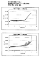
図5、図6によれば、ゲート絶縁膜の膜厚を一定とした場合、第二の段階で形成した絶縁膜の膜厚が大きくなるにつれ、リーク電流値は小さくなる。前記リーク電流値は小さくなる結果より、第二の段階で形成した絶縁膜は、第一の段階で形成した絶縁膜より絶縁性に優れていることが判る。なお、図5、図6中には、各TFT特性において、角5inch基板面内における10箇所の値を示しており、第一のTFT構造における特性値のバラツキは、絶縁膜膜質の、面内不均一性によるものと思われる。
【0051】
前記第二の段階で形成した絶縁膜のリーク電流値が小さくなる理由は、膜中窒素量によるものと考えられる。図14、図15にはCVDによりシリコンウエハ上に形成された絶縁膜のMOS電圧―リーク電流特性を示している。測定はそれぞれ電流密度1×10⁻⁶A/cm2において行った。図14には、絶縁膜中窒素濃度が大きいもの、すなわち窒素が主成分であり、窒素濃度として約37atomic%のものの特性を示し、図15には、絶縁膜中窒素濃度が小さいもの、すなわち膜中窒素原子が2×1020atomic/cm3である膜の特性を示している。 本発明のTFTではゲート絶縁膜は115nmであり、またこのTFTが液晶を駆動させるために用いられたとき、液晶を駆動させる電圧は20Vであることから、通常1.74MV/cmの電界がゲート絶縁膜にかかることになる。図14、図15においてこの電界でのリーク電流を比較すれば、絶縁膜中の窒素濃度が小さい方が、リーク電流は小さいと判断できる。
【0052】
また、図14から、窒素濃度が大きい絶縁膜の耐圧は、n型MOS、p型MOS、それぞれ6.4 MV/cm、6.5 MV/cmであるのに対し、図15から、窒素濃度が小さい絶縁膜の耐圧は、n型MOS、p型MOS、それぞれ7.3MV/cm、8.1 MV/cmである。この結果はゲート絶縁膜が115nmより薄い、もしくは高い電圧を印加した場合にも、絶縁膜中の窒素濃度が小さい方が良い絶縁特性を示している。
【0053】
以上の結果から、TFTにおいてシリコン上にゲート絶縁膜を形成する際、第一の段階で絶縁膜を形成することによりサブスレッショルド係数を良好にしたうえ、絶縁性に優れた第二の段階で絶縁膜を形成する前記第一のゲート絶縁膜の構造とすれば、サブスレッショルド係数において良好な特性であり、且つゲート電極―ソース電極もしくはゲート電極―ドレイン電極のリーク電流を押さえたTFT特性を得られると考えられる。
【0054】
第一の段階で絶縁膜を形成する目的は、非結晶シリコン表面が水素プラズマに曝露され、電荷をトラップする結合手を水素で終端することである。本発明者は第一の段階として、ターゲットにシリコンを用い、スパッタガスに水素と、N2Oと、Arと、を使用した。不活性ガスのArを流す以外に、N2Oを流した目的は、シリコン酸化窒化膜を形成し、不純物拡散を防ぐ為であるが、不純物拡散よりゲート電極―ドレイン電極のリーク電流をおさえたTFTを作製したいならば、N2Oの替わりにO2を流しても良い。したがってターゲットを適当なもの、例えばSiO2を用い、スパッタガスを適当なもの、例えば酸素と、水素と、を用いて同様の組成となる膜を形成しても第一の段階と同様の効果が期待できる。
【0055】
第二の段階で絶縁膜を形成する目的は、これによって絶縁性を向上させることである。この成膜は、図14,図15に示された通り、窒素流量の少ないスパッタガス雰囲気で形成する方法が有効である。好ましくは窒素原子を含まない雰囲気でスパッタする。第二の段階の例として、ターゲットにSiO2を用い、スパッタガスに酸素と、Arと、を使用しているが、ターゲットを適当なもの、例えばシリコンを用い、スパッタガスを適当なもの、例えば酸素と、Arと、を用いて同様の組成となる膜を形成しても、第二の段階と同じ効果が期待できる。
【0056】
特に、前記第一のゲート絶縁膜の構造において、HFS分析により膜中水素濃度を測定したとき0.4〜1.6atomic%である領域が存在し、且つ前記0.4〜1.6atomic%である領域の上層にHFS分析により膜中水素濃度を測定したとき0.2atomic%以下である領域が存在する様に形成し、作製したTFTにおいて、TFT特性を向上させるために水素化処理を行った場合、サブスレッショルド係数において、n-ch型TFTでは0.5〜0.7V/dec、p-ch型TFTでは0.5〜1.0V/dec、という良好な特性を示す。
【0057】
以上の構成からなる本発明について、以下に示す実施例でもってさらに詳細な説明を行うこととする。
【0058】
【実施例】
[実施例1]
本実施例ではプラスチック基板上にTFTを形成する作製工程について以下に説明する。
【0059】
まず、有機物からなるプラスチック基板201を用意する。本実施例では、ポリイミドからなる基板201を用いる。このポリイミドからなる基板の耐熱温度は約399℃であり、基板自体の色は透明ではなく、褐色である。次いで、基板201上に下地絶縁膜202を形成する。この下地絶縁膜はプロセス温度が300℃を越えない成膜方法であれば特に限定されず、ここではスパッタ法を用いて形成した。このスパッタ法ではスパッタガスに水素を含まない雰囲気において成膜するため、膜中水素量は5%以下である。
【0060】
次いで、非晶質半導体膜を形成し、レーザー照射により結晶化させて結晶質半導体膜を形成する。非晶質半導体膜はプロセス温度が300℃を越えない成膜方法であれば特に限定されず、ここではスパッタ法を用いて形成した。次いで、結晶質半導体膜を所望の形状にパターニングして半導体層203を形成する。
【0061】
次いで、半導体層203を覆うゲート絶縁膜204を形成する。ゲート絶縁膜はスパッタ法を用いて成膜する(図2(A))。このときシリコンターゲットをアルゴンと、酸素と、水素と、N2Oと、をスパッタガスとして用いてスパッタすることにより成膜する。好ましくは、スパッタガス及び流量はN2O/H2=40/30sccmとし、基板を加熱するガスとしてチャンバー内にArを10sccm流し、成膜電力を3kWとし、成膜圧力を0.4Paとする。このようにして形成された絶縁膜は、HFS分析により膜中水素濃度を測定したとき0.4〜1.6atomic%である領域が存在する。なお、この絶縁膜は形成されていれば良く、膜厚は望むべきTFT特性に応じて設計する。膜厚が厚いほど、ゲート電極―ソース電極もしくはゲート電極―ドレイン電極のリーク電流が大きくなる傾向にある。
【0062】
さらにその絶縁膜の上に、SiO2ターゲットをアルゴンと、酸素と、水素と、をスパッタガスとして用いてスパッタすることにより絶縁膜を成膜する。好ましくは、ターゲットにシリコンを用い、スパッタガス及び流量はN2O/H2=50/0sccmとし、基板を加熱するガスとしてチャンバー内にArを10sccm流し、成膜電力を3kWとし、成膜圧力を0.4Paとする。このようにして形成された絶縁膜は、HFS分析により膜中水素濃度を測定したとき0.2atomic%以下となる。
【0063】
次いで、ゲート電極205を形成する。(図2(B))ゲート電極205としては、Ta、W、Ti、Mo、Al、Cu、Cr、Ndから選ばれた元素、または前記元素を主成分とする合金材料若しくは化合物材料で形成してもよい。また、リン等の不純物元素をドーピングした多結晶シリコン膜に代表される半導体膜を用いてもよい。また、AgPdCu合金を用いてもよい。
【0064】
次いで、ゲート電極をマスクとしてゲート絶縁膜を自己整合的にエッチングしてゲート絶縁膜206を形成するとともに、半導体層の一部を露呈させてから半導体層の一部にn型を付与する不純物元素、ここではリンを添加(ドーピング)して不純物領域207を形成する(図2(C))。このときpチャネル型TFTにはレジストを形成しておき、前記p型を付与する不純物添加後に剥離する。
【0065】
次いで、ゲート電極をマスクとしてゲート絶縁膜を自己整合的にエッチングしてゲート絶縁膜を形成するとともに、半導体層の一部を露呈させてから半導体層の一部にp型を付与する不純物元素、ここではボロンを添加(ドーピング)して不純物領域208を形成する(図2(D))。このときnチャネル型TFTにはレジストを形成しておき、前記p型を付与する不純物添加後に剥離する。
【0066】
本実施例ではゲート絶縁膜のエッチングを行った後にドーピングを行ったが、ゲート電極を形成した後、ゲート絶縁膜を通過させてドーピングを行ってもよい。この場合、不純物元素はゲート絶縁膜を通過し、ゲート電極をマスクとして自己整合的にドーピングされる。
【0067】
次いで、層間絶縁膜210を形成し、ソース領域またはドレイン領域に達するコンタクトホールを形成した後、ソース領域に電気的に接続するソース配線211、ドレイン領域に電気的に接続する画素電極212を形成する。
【0068】
次いで、TFT特性を向上させるために水素化処理を行う。この水素化としては、水素雰囲気中での熱処理(350℃、1時間)、あるいは低温でプラズマ水素化を行う。
【0069】
以上の作製工程により、350℃以下のプロセス温度でプラスチック基板上にトップゲート型のTFTが完成する(図2(E))。
【0070】
[実施例2]
本発明では工程短縮、あるいは歩留まり向上等の理由で、画素部および駆動回路をすべて、nチャネル型TFTで形成してもよい。このときNチャネル型TFTを用いてNAND回路、NOR回路のような基本論理回路を構成したり、さらに複雑なロジック回路(信号分割回路、オペアンプ、γ補正回路など)をも構成することができる。
【0071】
なお、本実施例に示すTFTは、チャネル形成領域となる半導体に周期表の15族に属する元素(好ましくはリン)もしくは周期表の13族に属する元素(好ましくはボロン)を添加することによりエンハンスメント型とデプレッション型とを作り分けることができる。
【0072】
また、Nチャネル型TFTを組み合わせてNMOS回路を形成する場合、エンハンスメント型TFT同士で形成する場合(以下、EEMOS回路という)と、エンハンスメント型とデプレッション型とを組み合わせて形成する場合(以下、EDMOS回路という)がある。これらの回路を組み合わせて、液晶表示装置の駆動回路を全てNチャネル型TFTで構成することも可能である。
【0073】
[実施例3]
実施例1または2により得られるアクティブマトリクス基板を用いて液晶ディスプレイを作製する例を以下に示す。
【0074】
実施例1または2で作製された基板を、配向膜212形成、ラビング処理、配向膜216と対向電極215を備えた対向基板214の貼り合わせ、液晶213注入等の工程を経て反射型液晶表示装置が完成する(図7(A))。
【0075】
ここでは、画素電極212として、反射性を有する金属材料、例えばAl、Ag等を主成分とする材料を用いた。なお、本実施例では反射型の液晶表示装置の例を示したが、画素電極として透明導電膜、例えばITO(酸化インジウム酸化スズ合金)、酸化インジウム酸化亜鉛合金(In2O3―ZnO)、酸化亜鉛(ZnO)等を用いれば透過型液晶表示装置を形成することができる。
【0076】
図7(B)には上面図が示されている。画素部、駆動回路、FPC(フレキシブルプリント配線板:Flexible Printed Circuit)を貼り付ける外部入力端子、外部入力端子と各回路の入力部までを接続する配線81などが形成されたアクティブマトリクス基板と、カラーフィルタなどが設けられた対向基板82とがシール材83を介して貼り合わされている。
【0077】
ゲート側駆動回路84と重なるように対向基板側に遮光層86aが設けられ、ソース側駆動回路85と重なるように対向基板側に遮光層86bが形成されている。また、画素部87上の対向基板側に設けられたカラーフィルタ88は遮光層と、赤色(R)、緑色(G)、青色(B)の各色の着色層とが各画素に対応して設けられている。実際に表示する際には、赤色(R)の着色層、緑色(G)の着色層、青色(B)の着色層の3色でカラー表示を形成するが、これら各色の着色層の配列は任意なものとする。
【0078】
ここでは、カラー化を図るためにカラーフィルタ88を対向基板に設けているが特に限定されず、アクティブマトリクス基板を作製する際、アクティブマトリクス基板にカラーフィルタを形成してもよい。
【0079】
また、カラーフィルタにおいて隣り合う画素の間には遮光層が設けられており、表示領域以外の箇所を遮光している。また、ここでは、駆動回路を覆う領域にも遮光層86a、86bを設けているが、駆動回路を覆う領域は、後に液晶表示装置を電子機器の表示部として組み込む際、カバーで覆うため、特に遮光層を設けない構成としてもよい。また、アクティブマトリクス基板を作製する際、アクティブマトリクス基板に遮光層を形成してもよい。
【0080】
また、上記遮光層を設けずに、対向基板と対向電極の間に、カラーフィルタを構成する着色層を複数層重ねた積層で遮光するように適宜配置し、表示領域以外の箇所(各画素電極の間隙)や、駆動回路を遮光してもよい。
【0081】
また、外部入力端子にはベースフィルムと配線から成るFPC89が異方性導電性樹脂で貼り合わされている。さらに補強板で機械的強度を高めている。
【0082】
以上のようにして作製される液晶表示装置は各種電子機器の表示部として用いることができる。
【0083】
また、上記液晶表示装置におけるブロック図を図8に示す。なお、図8はアナログ駆動を行うための回路構成である。本実施例では、ソース側駆動回路90、画素部91及びゲート側駆動回路92を有している。なお、本明細書中において、駆動回路とはソース側処理回路およびゲート側駆動回路を含めた総称である。
【0084】
ソース側駆動回路90は、シフトレジスタ90a、バッファ90b、サンプリング回路(トランスファゲート)90cを設けている。また、ゲート側駆動回路92は、シフトレジスタ92a、レベルシフタ92b、バッファ92cを設けている。なお、シフトレジスタ90a、92aとしては図12に示したシフトレジスタを用いれば良い。また、必要であればサンプリング回路とシフトレジスタとの間にレベルシフタ回路を設けてもよい。
【0085】
また、本実施例において、画素部91は複数の画素を含み、その複数の画素に各々TFT素子が設けられている。
【0086】
これらソース側駆動回路90およびゲート側駆動回路92は全てNチャネル型TFTで形成され、全ての回路は図15(A)に示したEEMOS回路を基本単位として形成されている。ただし、従来のCMOS回路に比べると消費電力は若干上がってしまう。
【0087】
なお、図示していないが、画素部91を挟んでゲート側駆動回路92の反対側にさらにゲート側駆動回路を設けても良い。
【0088】
[実施例4]
本実施例では画素構造を図9に示し、断面構造を図10に示す。それぞれ、A−A’断面図、B−B’断面図を示した。
【0089】
本実施例では保持容量は、第2の半導体層1002上の絶縁膜を誘電体として、第2の半導体層1002と、容量電極1005とで形成している。なお、容量電極1005は、容量配線1009と接続されている。また、容量電極1005は、第1の電極1004及びソース配線1006と同じ絶縁膜上に同時に形成される。また、容量配線は、画素電極1011、接続電極1010、ゲート配線1007と同じ絶縁膜上に同時に形成される。
【0090】
また、本実施例では、不純物領域1012〜1014にはn型を付与する不純物元素が添加されている。なお、1012はソース領域、1013はドレイン領域である。
【0091】
また、本実施例では、ゲート電極とソース配線を同時に形成する例を示したが、マスクを1枚増やし、さらにゲート電極と第1の電極及び容量配線を別の工程で形成してもよい。即ち、まず、半導体層と重なりゲート電極となる部分だけを形成し、n型の不純物元素を添加し、低温での熱処理を行った後、ゲート電極と重ねて第1の電極を形成する。この際、コンタクトホールの形成を行うことなく、単なる重ね合わせでゲート電極と第1の電極とのコンタクトを形成する。また、第1の電極と同時にソース配線、容量配線を形成する。こうすることによって第1の電極及びソース配線の材料として低抵抗なアルミニウムや銅を用いることが可能となる。また、容量配線に重なる半導体層にn型の不純物元素を添加して保持容量の増加を図ることができる。
【0092】
なお、本実施例は実施例1乃至4のいずれか一と自由に組み合わせることができる。
【0093】
[実施例5]
本発明はアクティブマトリクス型ELディスプレイに適用することも可能である。その例を図11に示す。
【0094】
図11はアクティブマトリクス型ELディスプレイの回路図である。81は画素部を表しており、その周辺にはX方向制御回路82、Y方向制御回路83が設けられている。また、画素部81の各画素は、スイッチ用TFT84、コンデンサ85、電流制御用TFT86、有機EL素子87を有し、スイッチ用TFT84にX方向信号線88a(または88b)、Y方向信号線89a(または89b、89c)が接続される。また、電流制御用TFT86には、電源線90a、90bが接続される。
【0095】
本実施例のアクティブマトリクス型ELディスプレイでは、X方向制御回路82、Y方向制御回路83又は電流制御用TFT86として実施例1で作製されるCMOS回路を用い、スイッチ用TFT84として画素TFTを用いることが可能である。すなわち、本実施例のアクティブマトリクス型ELディスプレイは実施例1〜3で作製されるアクティブマトリクス基板を作製した後、公知の手段によりEL層を形成すれば良い。
【0096】
[実施例6]
本発明を実施して形成された駆動回路や画素部は様々な電気光学装置(アクティブマトリクス型液晶ディスプレイ、アクティブマトリクス型ELディスプレイ)に用いることができる。即ち、それら電気光学装置を表示部に組み込んだ電子機器全てに本発明を実施できる。
【0097】
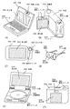
その様な電子機器としては、ビデオカメラ、デジタルカメラ、ヘッドマウントディスプレイ(ゴーグル型ディスプレイ)、パーソナルコンピュータ、携帯情報端末(モバイルコンピュータ、携帯電話または電子書籍等)などが挙げられる。
それらの一例を図12及び図13に示す。
【0098】
図12(A)はパーソナルコンピュータであり、本体2001、画像入力部2002、表示部2003、キーボード2004等を含む。本発明を画像入力部2002、表示部2003やその他の駆動回路に適用することができる。
【0099】
図12(B)はビデオカメラであり、本体2101、表示部2102、音声入力部2103、操作スイッチ2104、バッテリー2105、受像部2106等を含む。本発明を表示部2102やその他の駆動回路に適用することができる。
【0100】
図12(C)はモバイルコンピュータ(モービルコンピュータ)であり、本体2201、カメラ部2202、受像部2203、操作スイッチ2204、表示部2205等を含む。本発明は表示部2205やその他の駆動回路に適用できる。
【0101】
図12(D)はゴーグル型ディスプレイであり、本体2301、表示部2302、アーム部2303等を含む。本発明は表示部2302やその他の駆動回路に適用することができる。
【0102】
図12(E)はプログラムを記録した記録媒体(以下、記録媒体と呼ぶ)を用いるプレーヤーであり、本体2401、表示部2402、スピーカ部2403、記録媒体2404、操作スイッチ2405等を含む。なお、このプレーヤーは記録媒体としてDVD(Digtial Versatile Disc)、CD等を用い、音楽鑑賞や映画鑑賞やゲームやインターネットを行うことができる。本発明は表示部2402やその他の駆動回路に適用することができる。
【0103】
図12(F)はデジタルカメラであり、本体2501、表示部2502、接眼部2503、操作スイッチ2504、受像部(図示しない)等を含む。本発明を表示部2502やその他の駆動回路に適用することができる。
【0104】
図13(A)は携帯電話であり、本体2901、音声出力部2902、音声入力部2903、表示部2904、操作スイッチ2905、アンテナ2906等を含む。本発明を音声出力部2902、音声入力部2903、表示部2904やその他の駆動回路に適用することができる。
【0105】
図13(B)は携帯書籍(電子書籍)であり、本体3001、表示部3002、3003、記憶媒体3004、操作スイッチ3005、アンテナ3006等を含む。本発明は表示部3002、3003やその他の駆動回路に適用することができる。
【0106】
図13(C)はディスプレイであり、本体3101、支持台3102、表示部3103等を含む。本発明は表示部3103に適用することができる。本発明のディスプレイは特に大画面化した場合において有利であり、対角10インチ以上(特に30インチ以上)のディスプレイには有利である。
【0107】
以上の様に、本発明の適用範囲は極めて広く、あらゆる分野の電子機器に適用することが可能である。また、本実施例の電子機器は実施例1〜6のどのような組み合わせからなる構成を用いても実現することができる。
【0108】
【発明の効果】
本発明によれば、低温・短時間で電気光学装置を作製することができる。そのため、歩留まり及びスループットが向上し、製造コストを低減することが可能である。
【0109】
また、安価な電気光学装置を作製できるようになることで、それを表示部に用いる様々な電子機器を安価な価格で提供することができる。
【図面の簡単な説明】
【図1】 TFTの作製工程を示す図。
【図2】 TFTの作製工程を示す図。
【図3】 絶縁膜中の水素濃度を示すHFS分析結果を示す図。
【図4】 本発明におけるTFTのサブスレッショルド係数特性の比較。
【図5】 本発明におけるTFTの、ゲート−ソース間のリーク電流値の比較。
【図6】 本発明におけるTFTの、ゲート−ソース間のリーク電流値の比較。
【図7】 AM−LCDの作製工程及び外観を示す図。
【図8】 AM−LCDの回路ブロック図を示す図。
【図9】 画素部の上面図を示す図。
【図10】 画素部の断面図を示す図。
【図11】 アクティブマトリクス型EL表示装置の回路構成を示す図。
【図12】 電子機器の一例を示す図。
【図13】 電子機器の一例を示す図。
【図14】 絶縁膜中の窒素濃度が大きい場合の電圧―リーク電流特性
【図15】 絶縁膜中の窒素濃度が小さい場合の電圧―リーク電流特性[0001]
BACKGROUND OF THE INVENTION
The present invention relates to a method for manufacturing a semiconductor device having a circuit including thin film transistors (hereinafter referred to as TFTs). In particular, the present invention relates to a technique for manufacturing a TFT on a substrate having low heat resistance such as a plastic substrate. Note that in this specification, a semiconductor device refers to all devices that can function by utilizing semiconductor characteristics, and includes an electro-optical device, a semiconductor circuit, and an electronic device including them as a category of the semiconductor device.
[0002]
[Prior art]
Since a thin film transistor (hereinafter referred to as TFT) can be formed on a transparent substrate, application development to an active matrix liquid crystal display (hereinafter referred to as AM-LCD) is being actively promoted. Since a TFT using a semiconductor film having a crystal structure (hereinafter referred to as a crystalline semiconductor film) can obtain high mobility, it is possible to realize high-definition image display by integrating functional circuits on the same substrate. Has been. In particular, in an active matrix type display device as typified by a liquid crystal display device, a technique for forming not only a pixel portion but also a drive circuit with TFTs has been developed.
[0003]
Such display devices are manufactured in various sizes, and their application to portable electronic devices has attracted attention. Portable electronic devices are required to reduce the weight of individual components, and display devices are no exception. Until now, a glass plate having a thickness of about 1 mm has been used as a substrate for forming a display device. However, a method using a plastic substrate has been considered to reduce the weight.
[0004]
[Problems to be solved by the invention]
However, since the process temperature of a TFT using a crystalline semiconductor film is about 400 ° C., it is impossible to apply the technique as it is to a plastic substrate. In order to form a TFT on a plastic substrate, it is necessary to form a crystalline semiconductor film, a gate insulating film, or the like at approximately 300 ° C. or lower. A film formation technique by sputtering is one of techniques that can form not only a conductive film but also an insulating film and a semiconductor film at a relatively low temperature. However, attempts have been made to form a gate insulating film of a TFT by sputtering, but it has not always been possible to obtain good characteristics.
[0005]
A subthreshold coefficient (S value) can be increased as a guide for representing TFT characteristics. This is expressed from the relationship between the drain current and the gate voltage in the weak inversion state that flows when a voltage near or below the threshold voltage is applied to the gate electrode. Usually, the smaller the subthreshold coefficient, the faster the switching operation with lower power consumption becomes possible. The TFT characteristics when a gate insulating film is formed by sputtering are reported by, for example, Yodogawa (Jpn. J. Appl. Phys. Vol. 39 (2000) pp.L393-395)). , SiO 2 When a target was used to form a film with a sputtering gas of 30% oxygen and 70% argon, the S value was 2.5 V / dec for the n-channel TFT and 1.8 eV / dec for the p-channel TFT. It has been reported that dec was obtained.
[0006]
This S value is not always sufficient in consideration of the switching characteristics required for application to a display device or the like. There are various factors that can degrade TFT characteristics when a gate insulating film is formed by sputtering. However, as an important factor, it is important to control the concentration of hydrogen contained in the insulating film. It is done.
[0007]
In addition, since a large number of traps exist in the crystalline silicon layer or at the interface between the crystalline silicon and the gate insulating film, the threshold voltage (Vth) of the TFT is increased or high mobility cannot be obtained. There is. It is necessary to improve the film quality of the crystalline silicon film by diffusing hydrogen in the crystalline silicon layer or at the interface between the crystalline silicon and the gate insulating film to terminate the trap.
[0008]
Until now, TFTs have been manufactured by a film forming method in which the amount of hydrogen added to the film is controlled. For example, in Japanese Patent Laid-Open No. 10-0845085, a silicon nitride film containing hydrogen or an interlayer film made of a silicon nitride oxide film containing hydrogen is formed above a TFT, and the silicon nitride film or silicon nitride oxide film containing hydrogen is formed. It is shown that transistor characteristics can be stabilized by hydrogenation treatment with a lower substrate temperature by diffusing hydrogen into TFTs. However, in the case where the silicon nitride film or the silicon nitride oxide film containing hydrogen is formed by a film forming method in which the substrate processing temperature exceeds 400 ° C., it is difficult to apply the film to a plastic substrate.
[0009]
The present invention provides a technique for solving such problems, and improves the TFT characteristics by forming an insulating film by sputtering on a plastic substrate whose upper limit of the process temperature is limited to a low level. The purpose is to let you.
[0010]
[Means for Solving the Problems]
The present invention is characterized in that when forming a gate insulating film of a TFT using a sputtering method, the film forming conditions are divided into a first stage and a second stage. The first step is to form a film so that hydrogen is contained in the gate insulating film at a concentration of 0.4 to 1.6 atomic%. 2 A sputtering method using O and hydrogen as sputtering gases is employed. In the second stage, the gate insulating film is formed so that hydrogen is contained at a concentration of 0.2 atomic% or less. 2 A sputtering method using argon as a target and oxygen as sputtering gases is employed.
[0011]
The first stage is intended to contain hydrogen in the gate insulating film, and the second stage is intended to form a dense film with a low hydrogen content, and the hydrogen contained in the first stage. The purpose of this is to prevent the release to the outside. Therefore, the structure of the gate insulating film of the present invention is formed in a two-layer structure.
[0012]
By including hydrogen in the gate insulating film at the above concentration at the interface between the gate insulating film and the semiconductor layer and in the vicinity thereof, the defect density in the interface and the film can be reduced. Further, the internal stress can be relaxed (reduced) to reduce the stress applied to the semiconductor layer and its interface, and the shift of the threshold voltage as well as the S value can be suppressed. In addition, part of hydrogen contained in the region formed in the first stage of the gate insulating film can be diffused to contribute to hydrogenation of the semiconductor layer. The gate insulating film formed in the second stage is a relatively dense film, and confines the hydrogen formed in the first stage and prevents the diffusion to the outside, thereby retaining the effect of the hydrogen. Making it possible.
[0013]
The substrate temperature when forming the gate insulating film is set to 300 ° C. or lower in both the first stage and the second stage. As a result, the gate insulating film having the two-layer structure can be formed on the plastic substrate.
[0014]
As described above, a method for manufacturing a semiconductor device of the present invention includes a step of forming a semiconductor layer over an insulating surface, a step of forming a gate insulating film over the semiconductor layer, and a conductive layer over the gate insulating film. The step of forming the gate insulating film includes a step of forming Si or SiO on the target by sputtering. 2 A first step of forming a first insulating film containing Si, oxygen and nitrogen as main components and containing hydrogen at a concentration of 0.4 to 1.6 atomic%, and containing Si and oxygen as main components and hydrogen And a second step of forming a second insulating film containing 0.2% by atomic percent or less.
[0015]
In addition, since the present invention is characterized by film formation at a low temperature, it is very suitable for a plastic substrate, but can also be applied to a glass substrate or a quartz substrate. Even when applied to a glass substrate or a quartz substrate, effects such as cost reduction and throughput improvement due to a decrease in process temperature can be obtained.
[0016]
Representative techniques for measuring the hydrogen concentration in the film include SIMS analysis and hydrogen forward scattering (HFS) analysis. The HFS analysis is a method of irradiating a sample with He ions, measuring the energy of the scattered He ions, and quantifying the sample composition from the energy loss. The reason why the inventor measured the hydrogen concentration in the film by HFS analysis is that when the hydrogen concentration is about several percent as in the film of the present invention, the measurement error increases due to the matrix effect when measured by SIMS analysis. Therefore, it was judged that the HFS analysis was more appropriate. In the HFS analysis, He ions as a probe are irradiated with a sample within a range of φ5 to 10 mm. Measurement is possible if the film thickness is 10 nm or more in the range of φ5 to 10 mm. Even if the film to be analyzed by HFS has an opening or the like in the range of φ5 to 10 mm and has irregularities, the measurement can be performed although the influence of the substrate is present. Accordingly, in the completed semiconductor device, HFS analysis is possible if the upper layer of the film to be analyzed is peeled off and exposed.
[0017]
The HFS analysis performed in this specification has shown that hydrogen is contained at 0.2 atomic% or less in the second stage. This is an error of analysis, and hydrogen may be 0 atomic%.
[0018]
DETAILED DESCRIPTION OF THE INVENTION
Embodiments of the present invention will be described below. An example of the TFT manufacturing method of the present invention is shown in FIG.
[0019]
First, the
[0020]
The base
[0021]
Next, an amorphous semiconductor film is formed over the
[0022]
Next, the crystalline semiconductor film is patterned to form a
[0023]
Next, a
[0024]
Next, a
[0025]
Next, the gate insulating film is etched in a self-aligning manner using the
[0026]
Next, the gate insulating film is etched in a self-aligning manner using the gate electrode as a mask to form the gate insulating film, and an impurity element that imparts p-type to a part of the semiconductor layer after exposing a part of the semiconductor layer, Here, boron is added (doping) to form the impurity region 108 (FIG. 1E). At this time, a resist is formed on the n-channel TFT, and is peeled off after the impurity imparting the p-type is added.
[0027]
Next, an
[0028]
Next, hydrogenation is performed to improve TFT characteristics. As this hydrogenation, heat treatment in a hydrogen atmosphere or plasma hydrogenation at a low temperature is performed. Here, heat treatment is performed at 350 ° C. for one hour in a hydrogen atmosphere.
[0029]
Through the above manufacturing process, a top-gate TFT is completed on a plastic substrate at a process temperature of 350 ° C. or lower. Note that if plasma hydrogenation is performed at a low temperature by hydrogenation, a TFT is completed on a plastic substrate at a process temperature of 300 ° C. or lower.
[0030]
The inventor formed an insulating film in the first stage. FIG. 3 shows the result of measuring the hydrogen concentration in the insulating film formed in the first stage by HFS. FIG. 3A shows an HFS spectrum indicating the hydrogen concentration in the insulating film formed in the first stage. At this time, the detection angle with respect to the irradiated He ++ ion beam was 30 °, and the sample was 75 ° from the normal line. Further, Table 1 shows the concentration distribution in the depth direction obtained from FIG. The film formation conditions in the first stage are as follows. Silicon is used as the target, and the sputtering gas and flow rate are N. 2 O / H 2 = 40/30 sccm, Ar as a gas for heating the substrate, 10 sccm of Ar was flowed into the chamber, the deposition power was 3 kW, and the deposition pressure was 0.4 Pa.
[0031]
[Table 1]
From Table 1, it can be said that the hydrogen concentration in the film ranges from 0.4 to 1.6 atomic% from the measurement accuracy.
[0033]
The inventor has also disclosed that H in the sputtering gas in the chamber during film formation. 2 An insulating film was formed at a flow rate of 0 sccm. FIG. 3B similarly shows an HFS spectrum indicating the hydrogen concentration in the insulating film formed in the first stage. Further, the concentration distribution in the depth direction obtained from FIG. 3B is also shown in Table 1. The insulating film is formed using silicon as a target, and the sputtering gas and flow rate are N. 2 O / H 2 = 50/0 sccm, Ar as a gas for heating the substrate at a flow rate of 10 sccm, a deposition power of 3 kW, and a deposition pressure of 0.4 Pa. In Table 1, the hydrogen concentration in the film is 0.2 atomic% or less, which means the detection lower limit or less.
[0034]
That is, hydrogen in this film is H as a sputtering gas. 2 It was added by flowing. H 2 Is converted into plasma in the chamber, so that at least a gas containing hydrogen atoms as a sputtering gas does not flow, the hydrogen concentration in the film is considered to be 0.2 atomic% or less. Also in the first stage, the hydrogen concentration in the film is considered to be 0.2 atomic% or less unless a gas containing hydrogen atoms is allowed to flow as the sputtering gas.
[0035]
Thus, in this specification, the insulating film formed by sputtering using hydrogen gas can be specified from the hydrogen concentration by HFS analysis. The hydrogen concentration in the film ranges from 0.4 to 1.6 atomic% from the measurement accuracy.
[0036]
The present inventor manufactured and evaluated the TFT in the above process. The underlying SiO 2 , Amorphous semiconductor, gate insulating film, gate electrode, interlayer SiO 2 Sputter film formation was performed on each of the wiring and wiring layers, and the substrate temperature during film formation was 300 ° C. or lower.
[0037]
In order to compare the effects of hydrogenation in the gate insulating film during TFT evaluation, four structures of TFTs were fabricated.
[0038]
In the laminated structure of the gate insulating film, in order to facilitate the following description, a distinction is made between three gate insulating film structures. The structure of the first gate insulating film is a structure in which an insulating film is formed on the semiconductor layer in the first stage and an insulating film is formed on the second stage. The second gate insulating film has a structure in which an insulating film is formed in the second stage on the semiconductor layer. The third gate insulating film has a structure in which an insulating film is formed on the semiconductor layer in the first stage.
[0039]
The four structures of TFTs produced by the present inventors are shown below.
[0040]
In the first TFT structure, the gate insulating film is the structure of the second gate insulating film. At this time, the film thickness of the gate insulating film was 115 nm.
[0041]
In the second TFT structure, the gate insulating film has the structure of the first gate insulating film. At this time, the thickness of the insulating film formed in the first stage was 20 nm, and the thickness of the insulating film formed in the second stage was 95 nm.
[0042]
In the third TFT structure, the gate insulating film has the structure of the first gate insulating film. At this time, the thickness of the insulating film formed in the first stage was 4 nm, and the thickness of the insulating film formed in the second stage was 115 nm.
[0043]
In the fourth TFT structure, the gate insulating film has the structure of the third gate insulating film. At this time, the film thickness of the insulating film was 115 nm.
[0044]
In other words, the first TFT structure, the second TFT structure, the third TFT structure, and the fourth TFT structure are 115 nm and 20 nm in thickness of the insulating film formed in the first stage on the semiconductor upper layer, respectively. 4 nm and 0 nm are formed.
[0045]
In the third TFT structure, when the film was formed in the first stage, there was an intention to form a film thickness sufficiently thinner than 115 nm. Therefore, when the insulating film was formed in the second stage, the first The film thickness at this stage was ignored, and the total film thickness was 119 nm. Hereinafter, it is assumed that 4 nm is smaller than 115 nm, and the film thickness of the insulating film in the first to fourth TFT structures is 115 nm.
[0046]
FIG. 4, FIG. 5 and FIG. 6 show the TFT characteristics of the single gate and designed with length / width = 8/8 μm.
[0047]
In FIGS. 4A and 4B, the
[0048]
According to FIGS. 4A and 4B, when both the n-channel TFT and the p-channel TFT have a constant thickness of the gate insulating film, the insulating film formed in the second stage. It can be seen that the subthreshold coefficient increases as the thickness of the film increases. The reason why the subthreshold coefficient was improved when this insulating film containing hydrogen was used as the lower layer was that when the insulating film was formed, the surface of the amorphous silicon was exposed to hydrogen plasma, and a bond that traps charges was removed. This is thought to be due to the fact that the effect on the trap characteristics was reduced by terminating with hydrogen. In the experiment of the present inventor, the insulating film formed in the first stage has a minimum thickness of 4 nm. However, if plasma treatment is performed, there is a possibility that the TFT characteristics may be improved even if it is not formed on silicon.
[0049]
5 (a), 5 (b), 6 (a), and 6 (b), the
[0050]
According to FIGS. 5 and 6, when the thickness of the gate insulating film is constant, the leakage current value decreases as the thickness of the insulating film formed in the second stage increases. From the result that the leakage current value becomes small, it can be seen that the insulating film formed in the second stage is superior to the insulating film formed in the first stage. In FIGS. 5 and 6, the values of 10 locations in the corner of the 5-inch substrate are shown for each TFT characteristic. The variation in the characteristic values in the first TFT structure is the in-plane of the insulating film quality. This seems to be due to non-uniformity.
[0051]
The reason why the leakage current value of the insulating film formed in the second stage is small is considered to be due to the amount of nitrogen in the film. 14 and 15 show the MOS voltage-leakage current characteristics of an insulating film formed on a silicon wafer by CVD. Each measurement is
[0052]
Further, from FIG. 14, the breakdown voltage of the insulating film having a high nitrogen concentration is 6.4 MV / cm and 6.5 MV / cm for the n-type MOS and the p-type MOS, respectively. The breakdown voltage of n-type MOS and p-type MOS is 7.3 MV / cm and 8.1 MV / cm, respectively. This result shows that when the gate insulating film is thinner than 115 nm or a high voltage is applied, the smaller the nitrogen concentration in the insulating film, the better the insulating characteristics.
[0053]
From the above results, when forming the gate insulating film on the silicon in the TFT, the insulating film is formed in the first stage to improve the subthreshold coefficient, and the insulating is performed in the second stage having excellent insulating properties. If the structure of the first gate insulating film that forms the film is used, TFT characteristics that are excellent in the subthreshold coefficient and suppress the leakage current of the gate electrode-source electrode or the gate electrode-drain electrode can be obtained. it is conceivable that.
[0054]
The purpose of forming the insulating film in the first stage is to expose the amorphous silicon surface to hydrogen plasma and terminate the bond that traps charges with hydrogen. As a first step, the present inventor used silicon as a target, hydrogen as a sputtering gas, N 2 O and Ar were used. Besides flowing inert gas Ar, N 2 The purpose of flowing O is to form a silicon oxynitride film to prevent impurity diffusion, but if it is desired to manufacture a TFT in which the leakage current between the gate electrode and the drain electrode is suppressed by impurity diffusion, N 2 O instead of O 2 May be used. Therefore, the target should be a suitable one, eg SiO 2 Even if a film having the same composition is formed using a suitable sputtering gas, for example, oxygen and hydrogen, the same effect as in the first stage can be expected.
[0055]
The purpose of forming the insulating film in the second stage is to improve the insulating property. For this film formation, as shown in FIGS. 14 and 15, a method of forming in a sputtering gas atmosphere with a low nitrogen flow rate is effective. Sputtering is preferably performed in an atmosphere not containing nitrogen atoms. As an example of the second stage, the target is SiO 2 , Oxygen and Ar are used as the sputtering gas, but the same composition is used using an appropriate target, for example, silicon, and an appropriate sputtering gas, for example, oxygen and Ar. Even if the film to be formed is formed, the same effect as the second stage can be expected.
[0056]
In particular, in the structure of the first gate insulating film, there is a region that is 0.4 to 1.6 atomic% when the hydrogen concentration in the film is measured by HFS analysis, and the region is 0.4 to 1.6 atomic%. The hydrogen concentration in the film was formed so that there was a region of 0.2 atomic% or less when the hydrogen concentration in the film was measured by HFS analysis on the upper layer of a certain region, and the fabricated TFT was subjected to hydrogenation treatment to improve TFT characteristics In this case, in the sub-threshold coefficient, the n-ch TFT exhibits good characteristics of 0.5 to 0.7 V / dec, and the p-ch TFT exhibits 0.5 to 1.0 V / dec.
[0057]
The present invention having the above-described configuration will be described in more detail with the following examples.
[0058]
【Example】
[Example 1]
In this embodiment, a manufacturing process for forming a TFT over a plastic substrate will be described below.
[0059]
First, a
[0060]
Next, an amorphous semiconductor film is formed and crystallized by laser irradiation to form a crystalline semiconductor film. The amorphous semiconductor film is not particularly limited as long as the process temperature does not exceed 300 ° C., and is formed by sputtering here. Next, the
[0061]
Next, a gate insulating film 204 that covers the
[0062]
Furthermore, on the insulating film, SiO 2 An insulating film is formed by sputtering the target using argon, oxygen, and hydrogen as sputtering gases. Preferably, silicon is used as the target, and the sputtering gas and flow rate are N. 2 O / H 2 = 50/0 sccm, Ar as a gas for heating the substrate at a flow rate of 10 sccm, a deposition power of 3 kW, and a deposition pressure of 0.4 Pa. The insulating film formed in this way becomes 0.2 atomic% or less when the hydrogen concentration in the film is measured by HFS analysis.
[0063]
Next, the
[0064]
Next, the gate insulating film is etched in a self-aligning manner using the gate electrode as a mask to form the
[0065]
Next, the gate insulating film is etched in a self-aligning manner using the gate electrode as a mask to form the gate insulating film, and an impurity element that imparts p-type to a part of the semiconductor layer after exposing a part of the semiconductor layer, Here, boron is added (doping) to form the impurity region 208 (FIG. 2D). At this time, a resist is formed on the n-channel TFT, and is peeled off after the impurity imparting the p-type is added.
[0066]
In this embodiment, the doping is performed after the gate insulating film is etched. However, after the gate electrode is formed, the doping may be performed through the gate insulating film. In this case, the impurity element passes through the gate insulating film and is doped in a self-aligned manner using the gate electrode as a mask.
[0067]
Next, an
[0068]
Next, hydrogenation is performed to improve TFT characteristics. As this hydrogenation, heat treatment in a hydrogen atmosphere (350 ° C., 1 hour) or plasma hydrogenation is performed at a low temperature.
[0069]
Through the above manufacturing process, a top-gate TFT is completed over a plastic substrate at a process temperature of 350 ° C. or lower (FIG. 2E).
[0070]
[Example 2]
In the present invention, the pixel portion and the driver circuit may all be formed of n-channel TFTs for reasons such as process shortening or yield improvement. At this time, a basic logic circuit such as a NAND circuit or a NOR circuit can be formed using an N-channel TFT, or a more complex logic circuit (a signal dividing circuit, an operational amplifier, a γ correction circuit, or the like) can be formed.
[0071]
Note that the TFT shown in this embodiment is enhanced by adding an element belonging to Group 15 of the periodic table (preferably phosphorus) or an element belonging to Group 13 of the periodic table (preferably boron) to the semiconductor to be a channel formation region. A mold and a depletion mold can be created separately.
[0072]
When an NMOS circuit is formed by combining N-channel TFTs, an enhancement type TFT is formed (hereinafter referred to as an EEMOS circuit), or an enhancement type and a depression type are combined (hereinafter referred to as an EDMOS circuit). Called). By combining these circuits, the driving circuit of the liquid crystal display device can all be constituted by N-channel TFTs.
[0073]
[Example 3]
An example of manufacturing a liquid crystal display using the active matrix substrate obtained in Example 1 or 2 will be described below.
[0074]
The substrate manufactured in Example 1 or 2 is subjected to steps such as formation of the
[0075]
Here, as the
[0076]
FIG. 7B shows a top view. An active matrix substrate on which a pixel portion, a drive circuit, an external input terminal for attaching an FPC (Flexible Printed Circuit), a
[0077]
A
[0078]
Here, the
[0079]
In addition, a light-shielding layer is provided between adjacent pixels in the color filter to shield light other than the display area. Here, the light shielding layers 86a and 86b are also provided in the region covering the drive circuit. However, the region covering the drive circuit is covered with a cover when the liquid crystal display device is incorporated later as a display portion of an electronic device. It is good also as a structure which does not provide a light shielding layer. Further, when the active matrix substrate is manufactured, a light shielding layer may be formed on the active matrix substrate.
[0080]
Further, without providing the light-shielding layer, the light-shielding layer is appropriately disposed between the counter substrate and the counter electrode so as to be shielded from light by stacking a plurality of colored layers constituting the color filter. Or the drive circuit may be shielded from light.
[0081]
An FPC 89 made of a base film and wiring is bonded to the external input terminal with an anisotropic conductive resin. Furthermore, the mechanical strength is increased by the reinforcing plate.
[0082]
The liquid crystal display device manufactured as described above can be used as a display portion of various electronic devices.
[0083]
A block diagram of the liquid crystal display device is shown in FIG. FIG. 8 shows a circuit configuration for performing analog driving. In this embodiment, a source side driver circuit 90, a pixel portion 91, and a gate
[0084]
The source side driver circuit 90 includes a
[0085]
In this embodiment, the pixel portion 91 includes a plurality of pixels, and each of the plurality of pixels is provided with a TFT element.
[0086]
The source side driver circuit 90 and the gate
[0087]
Although not shown, a gate side drive circuit may be further provided on the opposite side of the gate
[0088]
[Example 4]
In this embodiment, the pixel structure is shown in FIG. 9, and the cross-sectional structure is shown in FIG. AA ′ sectional view and BB ′ sectional view are shown, respectively.
[0089]
In this embodiment, the storage capacitor is formed of the second semiconductor layer 1002 and the
[0090]
In this embodiment, an impurity element imparting n-type is added to the
[0091]
Further, although an example in which the gate electrode and the source wiring are formed at the same time has been described in this embodiment, the number of masks may be increased by one, and the gate electrode, the first electrode, and the capacitor wiring may be formed in another process. That is, first, only a portion that overlaps with a semiconductor layer and becomes a gate electrode is formed, an n-type impurity element is added, heat treatment is performed at a low temperature, and then a first electrode is formed so as to overlap with the gate electrode. At this time, the contact between the gate electrode and the first electrode is formed by simple superposition without forming a contact hole. In addition, a source wiring and a capacitor wiring are formed simultaneously with the first electrode. This makes it possible to use low resistance aluminum or copper as the material for the first electrode and the source wiring. In addition, an n-type impurity element can be added to the semiconductor layer overlapping the capacitor wiring to increase the storage capacitor.
[0092]
Note that this embodiment can be freely combined with any one of
[0093]
[Example 5]
The present invention can also be applied to an active matrix EL display. An example is shown in FIG.
[0094]
FIG. 11 is a circuit diagram of an active matrix EL display.
[0095]
In the active matrix EL display of this embodiment, the CMOS circuit manufactured in
[0096]
[Example 6]
The driver circuit and the pixel portion formed by implementing the present invention can be used for various electro-optical devices (active matrix liquid crystal display, active matrix EL display). That is, the present invention can be implemented in all electronic devices in which these electro-optical devices are incorporated in the display unit.
[0097]
Examples of such an electronic device include a video camera, a digital camera, a head mounted display (goggles type display), a personal computer, a portable information terminal (mobile computer, mobile phone, electronic book, etc.), and the like.
Examples of these are shown in FIGS.
[0098]
FIG. 12A illustrates a personal computer, which includes a main body 2001, an image input portion 2002, a display portion 2003, a
[0099]
FIG. 12B illustrates a video camera, which includes a main body 2101, a display portion 2102, an
[0100]
FIG. 12C illustrates a mobile computer, which includes a main body 2201, a camera unit 2202, an
[0101]
FIG. 12D shows a goggle type display, which includes a
[0102]
FIG. 12E shows a player using a recording medium (hereinafter referred to as a recording medium) on which a program is recorded, which includes a main body 2401, a
[0103]
FIG. 12F illustrates a digital camera, which includes a main body 2501, a
[0104]
FIG. 13A shows a mobile phone, which includes a
[0105]
FIG. 13B illustrates a portable book (electronic book), which includes a
[0106]
FIG. 13C shows a display, which includes a
[0107]
As described above, the application range of the present invention is extremely wide and can be applied to electronic devices in various fields. Moreover, the electronic device of a present Example is realizable even if it uses the structure which consists of what combination of Examples 1-6.
[0108]
【The invention's effect】
According to the present invention, an electro-optical device can be manufactured at a low temperature and in a short time. Therefore, yield and throughput can be improved, and manufacturing costs can be reduced.
[0109]
In addition, since an inexpensive electro-optical device can be manufactured, various electronic devices using the electro-optical device for the display portion can be provided at a low price.
[Brief description of the drawings]
FIGS. 1A and 1B illustrate a manufacturing process of a TFT. FIGS.
FIGS. 2A and 2B are diagrams illustrating a manufacturing process of a TFT. FIGS.
FIG. 3 is a diagram showing an HFS analysis result showing a hydrogen concentration in an insulating film.
FIG. 4 is a comparison of sub-threshold coefficient characteristics of TFTs according to the present invention.
FIG. 5 is a comparison of gate-source leakage current values of TFTs according to the present invention.
FIG. 6 is a comparison of gate-source leakage current values of TFTs according to the present invention.
7A and 7B are diagrams illustrating a manufacturing process and an appearance of an AM-LCD.
FIG. 8 is a circuit block diagram of an AM-LCD.
FIG. 9 is a top view of a pixel portion.
FIG. 10 is a cross-sectional view of a pixel portion.
FIG. 11 illustrates a circuit configuration of an active matrix EL display device.
FIG 12 illustrates an example of an electronic device.
FIG 13 illustrates an example of an electronic device.
FIG. 14 shows voltage-leakage current characteristics when the nitrogen concentration in the insulating film is large.
FIG. 15 shows voltage-leakage current characteristics when the nitrogen concentration in the insulating film is low.
Claims (6)
前記半導体層上にゲート絶縁膜を形成し、
前記ゲート絶縁膜上に導電層を形成する半導体装置の作製方法であって、
前記ゲート絶縁膜は第1絶縁膜と前記第1絶縁膜上の第2絶縁膜との積層でなり、
前記第1絶縁膜は、スパッタ法により、Si、酸素、窒素を主成分とし、水素を0.4〜1.6atomic%の濃度で含有するように作製し、
前記第2絶縁膜は、スパッタ法により、Si、酸素を主成分とし、水素を0.2atomic%以下の濃度で含有するように作製することを特徴とする半導体装置の作製方法。Forming a semiconductor layer on the insulating surface;
Forming a gate insulating film on the semiconductor layer;
A method for manufacturing a semiconductor device in which a conductive layer is formed over the gate insulating film ,
The gate insulating film is a stack of a first insulating film and a second insulating film on the first insulating film,
The first insulating film, by sputtering, and S i, oxygen, nitrogen as a main component, to produce a hydrogen to contain a concentration of 0.4~1.6Atomic%,
The second insulating film, by sputtering, Si, a method for manufacturing a semiconductor device which oxygen as a main component, characterized in that to produce hydrogen so as to contain a concentration of less than 0.2 atomic%.
前記第1の絶縁膜は、ターゲットにSiを用い、スパッタガスとして希ガスと水素とNThe first insulating film uses Si as a target, and a rare gas, hydrogen, and N as sputtering gases. 22 Oを用いることによって作製することを特徴とする半導体装置の作製方法。A method for manufacturing a semiconductor device, which is manufactured by using O.
前記第2絶縁膜は、ターゲットにSiO2を用い、スパッタガスとして希ガスと酸素とを用いることによって作製することを特徴とする半導体装置の作製方法。In claim 1 or claim 2 ,
The method of manufacturing a semiconductor device, wherein the second insulating film is manufactured by using SiO 2 as a target and using a rare gas and oxygen as sputtering gases.
前記第2絶縁膜は、ターゲットにSiを用い、スパッタガスとして希ガスと酸素とを用いることによって作製することを特徴とする半導体装置の作製方法。In claim 1 or claim 2 ,
The method of manufacturing a semiconductor device, wherein the second insulating film is manufactured by using Si as a target and using a rare gas and oxygen as sputtering gases.
前記ゲート絶縁膜を形成した後、前記半導体層を350℃以下で水素化することを特徴とする半導体装置の作製方法。In any one of Claims 1 thru | or 4 ,
After forming the gate insulating film, a method for manufacturing a semiconductor device comprising a benzalkonium be hydrogenated at 350 ° C. below the semiconductor layer.
前記絶縁表面は、プラスチック基板上に設けられた絶縁膜表面であることを特徴とする半導体装置の作製方法。In any one of Claims 1 thru | or 5 ,
The method for manufacturing a semiconductor device, wherein the insulating surface is an insulating film surface provided over a plastic substrate.
Priority Applications (2)
| Application Number | Priority Date | Filing Date | Title |
|---|---|---|---|
| JP2001041028A JP4663139B2 (en) | 2001-02-16 | 2001-02-16 | Method for manufacturing semiconductor device |
| US10/071,211 US6620658B2 (en) | 2001-02-16 | 2002-02-11 | Method of manufacturing a semiconductor device |
Applications Claiming Priority (1)
| Application Number | Priority Date | Filing Date | Title |
|---|---|---|---|
| JP2001041028A JP4663139B2 (en) | 2001-02-16 | 2001-02-16 | Method for manufacturing semiconductor device |
Publications (3)
| Publication Number | Publication Date |
|---|---|
| JP2002246602A JP2002246602A (en) | 2002-08-30 |
| JP2002246602A5 JP2002246602A5 (en) | 2008-01-31 |
| JP4663139B2 true JP4663139B2 (en) | 2011-03-30 |
Family
ID=18903529
Family Applications (1)
| Application Number | Title | Priority Date | Filing Date |
|---|---|---|---|
| JP2001041028A Expired - Fee Related JP4663139B2 (en) | 2001-02-16 | 2001-02-16 | Method for manufacturing semiconductor device |
Country Status (2)
| Country | Link |
|---|---|
| US (1) | US6620658B2 (en) |
| JP (1) | JP4663139B2 (en) |
Families Citing this family (15)
| Publication number | Priority date | Publication date | Assignee | Title |
|---|---|---|---|---|
| TWI288443B (en) | 2002-05-17 | 2007-10-11 | Semiconductor Energy Lab | SiN film, semiconductor device, and the manufacturing method thereof |
| JP2004071696A (en) * | 2002-08-02 | 2004-03-04 | Semiconductor Energy Lab Co Ltd | Semiconductor device and manufacturing method thereof |
| US7605023B2 (en) * | 2002-08-29 | 2009-10-20 | Semiconductor Energy Laboratory Co., Ltd. | Manufacturing method for a semiconductor device and heat treatment method therefor |
| JP4627961B2 (en) * | 2002-09-20 | 2011-02-09 | 株式会社半導体エネルギー研究所 | Method for manufacturing semiconductor device |
| CA2499944A1 (en) * | 2002-09-30 | 2004-04-15 | Nanosys, Inc. | Integrated displays using nanowire transistors |
| US7300829B2 (en) * | 2003-06-02 | 2007-11-27 | Applied Materials, Inc. | Low temperature process for TFT fabrication |
| KR100623229B1 (en) | 2003-11-29 | 2006-09-18 | 삼성에스디아이 주식회사 | Organic electroluminescent display and manufacturing method thereof |
| KR100612868B1 (en) * | 2004-11-08 | 2006-08-14 | 삼성전자주식회사 | Silicon film manufacturing method |
| KR100731745B1 (en) | 2005-06-22 | 2007-06-22 | 삼성에스디아이 주식회사 | Organic light emitting display device and manufacturing method |
| JP4992232B2 (en) * | 2005-11-30 | 2012-08-08 | 凸版印刷株式会社 | THIN FILM TRANSISTOR, MANUFACTURING METHOD THEREOF, AND FILM-FORMING APPARATUS |
| JP5616038B2 (en) | 2008-07-31 | 2014-10-29 | 株式会社半導体エネルギー研究所 | Method for manufacturing semiconductor device |
| JP2010245366A (en) * | 2009-04-08 | 2010-10-28 | Fujifilm Corp | Electronic device, method for manufacturing the same, and display device |
| EP2428994A1 (en) * | 2010-09-10 | 2012-03-14 | Applied Materials, Inc. | Method and system for depositing a thin-film transistor |
| US20130300978A1 (en) * | 2012-05-14 | 2013-11-14 | Apple Inc. | Display with Minimized Light Leakage |
| CN110828486B (en) * | 2019-11-19 | 2023-05-12 | 云谷(固安)科技有限公司 | Manufacturing method of display panel and display panel |
Family Cites Families (18)
| Publication number | Priority date | Publication date | Assignee | Title |
|---|---|---|---|---|
| JPH03241874A (en) * | 1990-02-20 | 1991-10-29 | Seiko Epson Corp | Method for manufacturing thin film semiconductor devices |
| TW237562B (en) | 1990-11-09 | 1995-01-01 | Semiconductor Energy Res Co Ltd | |
| CN100367461C (en) | 1993-11-05 | 2008-02-06 | 株式会社半导体能源研究所 | A method of manufacturing thin film transistors and electronic devices |
| JP3468848B2 (en) * | 1994-06-09 | 2003-11-17 | 株式会社半導体エネルギー研究所 | Thin film transistor and method for manufacturing the same, and liquid crystal display device and method for manufacturing the same |
| TW371796B (en) | 1995-09-08 | 1999-10-11 | Semiconductor Energy Lab Co Ltd | Method and apparatus for manufacturing a semiconductor device |
| JP2652368B2 (en) * | 1996-04-05 | 1997-09-10 | 株式会社半導体エネルギー研究所 | Method for manufacturing insulated gate semiconductor device |
| JPH1084085A (en) | 1996-09-09 | 1998-03-31 | Matsushita Electron Corp | Semiconductor device and its method of manufacturing the same. |
| US6277679B1 (en) * | 1998-11-25 | 2001-08-21 | Semiconductor Energy Laboratory Co., Ltd. | Method of manufacturing thin film transistor |
| TW518637B (en) | 1999-04-15 | 2003-01-21 | Semiconductor Energy Lab | Electro-optical device and electronic equipment |
| TW517260B (en) | 1999-05-15 | 2003-01-11 | Semiconductor Energy Lab | Semiconductor device and method for its fabrication |
| CN100505313C (en) | 1999-12-10 | 2009-06-24 | 株式会社半导体能源研究所 | Semiconductor device and manufacturing method thereof |
| US6639265B2 (en) | 2000-01-26 | 2003-10-28 | Semiconductor Energy Laboratory Co., Ltd. | Semiconductor device and method of manufacturing the semiconductor device |
| JP2001250956A (en) | 2000-03-08 | 2001-09-14 | Semiconductor Energy Lab Co Ltd | Semiconductor device |
| US7503975B2 (en) | 2000-06-27 | 2009-03-17 | Semiconductor Energy Laboratory Co., Ltd. | Semiconductor device and fabrication method therefor |
| TW545080B (en) | 2000-12-28 | 2003-08-01 | Semiconductor Energy Lab | Light emitting device and method of manufacturing the same |
| TW525402B (en) | 2001-01-18 | 2003-03-21 | Semiconductor Energy Lab | Process for producing a light emitting device |
| SG107573A1 (en) | 2001-01-29 | 2004-12-29 | Semiconductor Energy Lab | Light emitting device |
| SG143945A1 (en) | 2001-02-19 | 2008-07-29 | Semiconductor Energy Lab | Light emitting device and method of manufacturing the same |
-
2001
- 2001-02-16 JP JP2001041028A patent/JP4663139B2/en not_active Expired - Fee Related
-
2002
- 2002-02-11 US US10/071,211 patent/US6620658B2/en not_active Expired - Fee Related
Also Published As
| Publication number | Publication date |
|---|---|
| US20020160554A1 (en) | 2002-10-31 |
| US6620658B2 (en) | 2003-09-16 |
| JP2002246602A (en) | 2002-08-30 |
Similar Documents
| Publication | Publication Date | Title |
|---|---|---|
| KR100816270B1 (en) | Electro-optical device and method of manufacturing same | |
| JP5708910B2 (en) | THIN FILM TRANSISTOR, MANUFACTURING METHOD THEREOF, AND DISPLAY DEVICE | |
| JP4663139B2 (en) | Method for manufacturing semiconductor device | |
| US7745271B2 (en) | Method of manufacturing a semiconductor device | |
| JP4678933B2 (en) | Method for manufacturing semiconductor device | |
| US11283039B2 (en) | Display substrate with improved carrier mobility of thin film transistors within GOA region | |
| JP2003273361A (en) | Semiconductor device and manufacturing method thereof | |
| TW201030924A (en) | Display device and method for manufacturing the same | |
| JP2001036019A (en) | Capacitor, semiconductor device, and manufacturing method thereof | |
| JP4641582B2 (en) | Method for manufacturing semiconductor device | |
| JP4993826B2 (en) | Method for manufacturing semiconductor device | |
| JP4683696B2 (en) | Method for manufacturing semiconductor device | |
| JP6291015B2 (en) | Semiconductor device | |
| JP4850763B2 (en) | Method for manufacturing semiconductor device | |
| CN101478004B (en) | Thin film transistor and semiconductor device and electronic device | |
| JP5577384B2 (en) | Method for manufacturing semiconductor device | |
| JP4986347B2 (en) | Method for manufacturing semiconductor device | |
| JP4583654B2 (en) | Method for manufacturing semiconductor device | |
| CN111785734A (en) | a backplane system | |
| JP4712155B2 (en) | Method for manufacturing semiconductor device | |
| CN115050757B (en) | Display panel and display device | |
| JP4700159B2 (en) | Method for manufacturing semiconductor device | |
| JP2002222954A (en) | Electro-optical device and manufacturing method thereof |
Legal Events
| Date | Code | Title | Description |
|---|---|---|---|
| A521 | Request for written amendment filed |
Free format text: JAPANESE INTERMEDIATE CODE: A523 Effective date: 20071205 |
|
| A621 | Written request for application examination |
Free format text: JAPANESE INTERMEDIATE CODE: A621 Effective date: 20071205 |
|
| TRDD | Decision of grant or rejection written | ||
| A01 | Written decision to grant a patent or to grant a registration (utility model) |
Free format text: JAPANESE INTERMEDIATE CODE: A01 Effective date: 20101221 |
|
| A01 | Written decision to grant a patent or to grant a registration (utility model) |
Free format text: JAPANESE INTERMEDIATE CODE: A01 |
|
| A977 | Report on retrieval |
Free format text: JAPANESE INTERMEDIATE CODE: A971007 Effective date: 20101222 |
|
| A61 | First payment of annual fees (during grant procedure) |
Free format text: JAPANESE INTERMEDIATE CODE: A61 Effective date: 20110105 |
|
| R150 | Certificate of patent or registration of utility model |
Free format text: JAPANESE INTERMEDIATE CODE: R150 |
|
| FPAY | Renewal fee payment (event date is renewal date of database) |
Free format text: PAYMENT UNTIL: 20140114 Year of fee payment: 3 |
|
| R250 | Receipt of annual fees |
Free format text: JAPANESE INTERMEDIATE CODE: R250 |
|
| R250 | Receipt of annual fees |
Free format text: JAPANESE INTERMEDIATE CODE: R250 |
|
| R250 | Receipt of annual fees |
Free format text: JAPANESE INTERMEDIATE CODE: R250 |
|
| R250 | Receipt of annual fees |
Free format text: JAPANESE INTERMEDIATE CODE: R250 |
|
| LAPS | Cancellation because of no payment of annual fees |