Low-power consumption bandwidth multiplication chopped wave stabilizing operational amplifier based on the MOS device
Technical field
The invention belongs to the analog integrated circuit design field, particularly a kind of low-power consumption bandwidth multiplication chopped wave stabilizing operational amplifier based on the MOS device.
Background technology:
Since 20 centurial years generations, increasingly mature along with the development of sub-micron, sub-micro technology and system chip technology adopted battery powered portable type electronic product to obtain fast development and popularizes fast.Because the development of battery technology does not catch up with the development with electronic system far away, from the cardiac pacemaker to the hearing aids, mobile phone and variety of products all proposed strict restriction to the supply power voltage of electronic product.On the other hand, along with device size constantly dwindles, the puncture voltage of technique also reducing, has also proposed strict restriction to supply voltage.The electronic device performance requirement is more and more higher, and the construction cycle is shorter and shorter, and is also increasingly strict with the restriction of production cost to exploitation, makes the low-voltage simulation integrated circuit receive great concern.
Operational amplifier is most important circuit unit in the analog circuit, is widely used in analog circuit and the mixed signal treatment circuit, and such as switching capacity, modulus, digital to analog converter etc.But linearity does not reduce along with reducing of characteristic size owing to transistorized threshold voltage, so under the low supply voltage environment, the every new of operational amplifier can index can reduce greatly.In order to improve the performance of amplifier, the bandwidth range of increasing circuit processing signals just must improve design to traditional folded common source and common grid amplifier, and this has just facilitated generation and the development of various novel low-power consumption wide-band amplifiers.Under environment under low pressure, the impact of operational amplifier low-frequency noise can increase simultaneously.In order to improve the noiseproof feature of amplifier, increase the signal to noise ratio of signal, just must improve design to the structure of amplifier, this has just facilitated generation and the development of chopper stabilized amplifier.
In recent years, low-power consumption broadband chopped wave stabilizing operational amplifier emerged in multitude, and each major company also releases own corresponding product one after another.Its application is very extensive, can be used in the middle of DVD player, sound card, mobile phone, system, the various circuit of sensor.Traditional folded common source and common grid chopper stabilized amplifier mainly has following characteristics: (1) low frequency 1/f noise is well suppressed.(2) have higher low-frequency gain and wider bandwidth.(3) output voltage can reach the positive and negative two-stage of supply voltage.
The circuit structure of traditional chopped wave stabilizing folded common source and common grid amplifier as shown in Figure 1.Input signal is first through a frequency mixer, then enter the input stage of amplifier, input stage is comprised of two PMOS pipe P1, P2, and electric current with positive and negative both direction is folding simultaneously flows through N3, N4 to positive-negative output end for it, at last the output of amplifier again through a frequency mixer to output.Wherein, NMOS pipe N1, N2 play the effect of current source.But traditional chopped wave stabilizing folded common source and common grid amplifier has the following disadvantages:
1. than the amplifier of other types, its quiescent dissipation is high.
2. current source N1, N2 just serve as current source, are not utilized the transmission small-signal current, are a kind of " wastes ".
3. in the strict situation of power consumption, be difficult to reach the performance of high bandwidth.
Summary of the invention
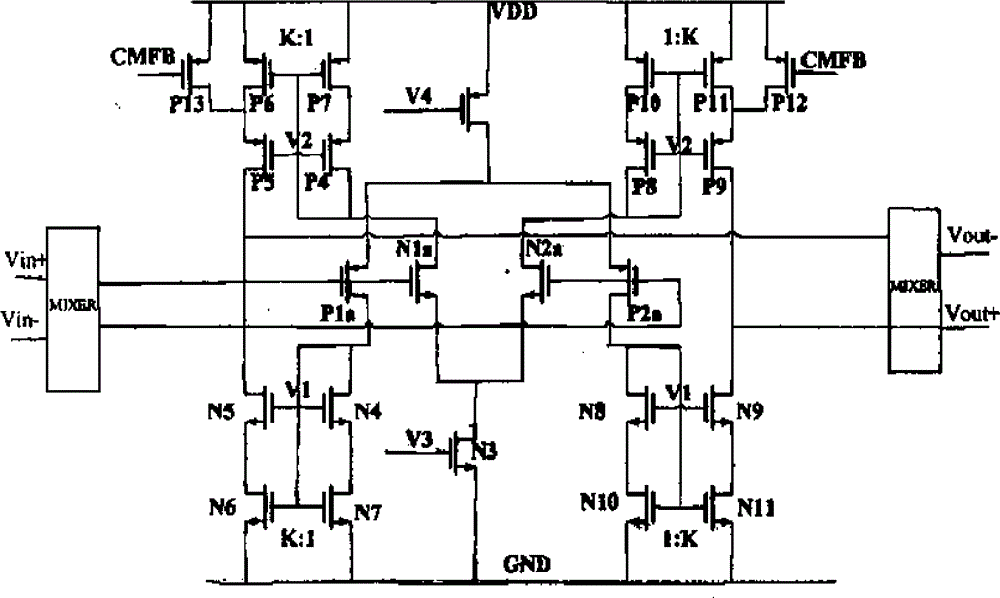
The objective of the invention is for overcoming the weak point of prior art, a kind of low-power consumption bandwidth multiplication chopped wave stabilizing operational amplifier based on the MOS device is proposed, it is characterized in that described low-power consumption bandwidth multiplication chopped wave stabilizing operational amplifier comprises two frequency mixers, shunting input stage, the amplify intergrade and the rail-to-rail output stage that reclaim electric current; Wherein in two frequency mixers one place before the amplifier input stage, another places after the amplifier output stage, realizes raising frequency and frequency-dropping function to input signal; The shunting input stage manages P1a, P2a by PMOS and NMOS pipe N1b, N2b form; The intergrade that electric current is reclaimed in described amplification comprises the first current mirror that is comprised of NMOS pipe N4, N6, N7, the second current mirror that is comprised of NMOS pipe N8, N10, N11 is managed the 3rd current mirror that P4, P6, P7 form and the 4th current mirror that is comprised of P8, P10, P11 by PMOS; Described rail-to-rail output stage is comprised of NMOS pipe N5, N9 and PMOS pipe P5, P9;
The positive and negative input signal of described low-power consumption bandwidth multiplication chopped wave stabilizing operational amplifier carries out mixing by a frequency mixer first, signal is modulated in the carrier frequency band scope, then the forward input signal converts voltage signal to downward current signal by input pipe P1a, this signal code is exaggerated K doubly by the first current mirror that is comprised of NMOS pipe N4, N6, N7, then flows to the negative sense output by N5; Simultaneously, the forward input signal converts voltage signal to upwards current signal by input pipe N1b, and this signal code is exaggerated K doubly by the 3rd current mirror that is comprised of PMOS pipe P4, P6, P7, then also flows to the negative sense output by P5; The negative sense input signal converts voltage signal to downward current signal by input pipe P2a, and this signal code is exaggerated K doubly by the second current mirror that is comprised of NMOS pipe N8, N10, N11, then flows to the forward output by N9; Simultaneously, the negative sense input signal converts voltage signal to upwards current signal by input pipe N2b, this signal code is exaggerated K doubly by the second current mirror that is comprised of NMOS pipe N8, N10, N11, then also flow to the forward output by P9, last positive negative output signal modulates the signal near the base band again through a frequency mixer; Wherein each metal-oxide-semiconductor adopts conventional MOS transistor, or adopts the strain silicon MOS pipe of high mobility, with the performance of further this circuit of raising.
The PMOS pipe of described input stage should keep its mutual conductance consistent with the NMOS pipe, and then the size of PMOS pipe is the twice of the size of NMOS pipe.
Described the first current mirror that is comprised of NMOS pipe N4, N6, N7 is connected with the P1a pipe drain electrode of input stage, the second current mirror that is comprised of NMOS pipe N8, N10, N11 is connected with the P2a pipe drain electrode of input stage, the 3rd current mirror that is comprised of PMOS pipe P4, P6, P7 is connected with the N1b pipe drain electrode of input stage, and the 4th current mirror that is comprised of PMOS pipe P8, P10, P11 is connected with the N2b pipe drain electrode of input stage.
This novel low-power consumption bandwidth multiplication chopped wave stabilizing operational amplifier of the present invention is compared with the traditional design scheme has following obvious advantage: have the ability that improves nearly three times of bandwidth in the situation of not obvious increase power consumption; Reduce the low frequency 1/f noise; Increase low-frequency gain; Simultaneously can also be in the plurality of advantages such as above power consumption that are at half such as the hydraulic performance decline that keeps same bandwidth, noise.
Description of drawings:
Fig. 1 is the circuit structure diagram of traditional folded common source and common grid chopper stabilized amplifier.
Fig. 2 is the circuit structure diagram of Novel low power consumption bandwidth multiplication chopped wave stabilizing operational amplifier of the present invention.
Fig. 3 is the frequency response simulation comparison figure of Novel low power consumption bandwidth multiplication chopped wave stabilizing operational amplifier of the present invention and traditional amplifier.
Embodiment:
Low-power consumption bandwidth multiplication chopped wave stabilizing operational amplifier based on the MOS device provided by the invention, a kind of embodiment adopts CMOS technique to realize.In Fig. 2, described low-power consumption bandwidth multiplication chopped wave stabilizing operational amplifier comprises two frequency mixers, shunting input stage, the amplify intergrade and the rail-to-rail output stage that reclaim electric current; Wherein in two frequency mixers one place before the amplifier input stage, another places after the amplifier output stage, realizes raising frequency and frequency-dropping function to input signal; The shunting input stage manages P1a, P2a by PMOS and NMOS pipe N1b, N2b form; Wherein in order to keep the PMOS pipe consistent with the mutual conductance of NMOS pipe, the size of PMOS pipe is the twice of the size of NMOS pipe.The intergrade that electric current is reclaimed in described amplification comprises the first current mirror that is comprised of NMOS pipe N4, N6, N7, the second current mirror that is comprised of NMOS pipe N8, N10, N11 is managed the 3rd current mirror that P4, P6, P7 form and the 4th current mirror that is comprised of P8, P10, P11 by PMOS; Described rail-to-rail output stage is comprised of NMOS pipe N5, N9 and PMOS pipe P5, P9.Each metal-oxide-semiconductor of this low-power consumption bandwidth multiplication chopped wave stabilizing operational amplifier has following link structure:
Positive and negative input signal is connected with first frequency mixer, the forward output of first frequency mixer links to each other with the grid of P1a and N1a, the negative sense output of first frequency mixer links to each other with the grid of P2a and N2a, the drain electrode of P1a and N6, the grid of N7 links to each other, the drain electrode of N1a and P6, the grid of P7 links to each other, the drain electrode of N2a and P10, the grid of P11 links to each other, the drain electrode of P2a and N10, the grid of N11 links to each other, the drain electrode of P5 links to each other with the drain electrode of N5, then link to each other with the forward input of second mixing, the drain electrode of N9 links to each other with the drain electrode of P9, then links to each other with the negative sense input of second frequency mixer; The grid of P12 and P13 links to each other with common mode feedback amplifier CMFB together.
The operation principle of described low-power consumption bandwidth multiplication chopped wave stabilizing operational amplifier is that positive and negative input signal carries out the input that amplifier is delivered in mixing again by a frequency mixer first, and the positive negative output signal of last amplifier again carries out frequency reducing through another frequency mixer and delivers to output again.
As shown in Figure 2, positive and negative input signal carries out mixing by a frequency mixer first, signal is modulated in the carrier frequency band scope, then the forward input signal converts voltage signal to downward current signal by input pipe P1a, this signal code is exaggerated K doubly by the first current mirror that is comprised of NMOS pipe N4, N6, N7, then flows to the negative sense output by N5; Simultaneously, the forward input signal converts voltage signal to upwards current signal by input pipe N1b, and this signal code is exaggerated K doubly by the 3rd current mirror that is comprised of PMOS pipe P4, P6, P7, then also flows to the negative sense output by P5; The negative sense input signal converts voltage signal to downward current signal by input pipe P2a, and this signal code is exaggerated K doubly by the second current mirror that is comprised of NMOS pipe N8, N10, N11, then flows to the forward output by N9; Simultaneously, the negative sense input signal converts voltage signal to upwards current signal by input pipe N2b, this signal code is exaggerated K doubly by the second current mirror that is comprised of NMOS pipe N8, N10, N11, then also flow to the forward output by P9, then also flow to the negative sense output by P5, mix down to output finally by crossing frequency mixer.Can get thus, the input equivalent transconductance has been exaggerated 2K doubly.Among the present invention, the value of K is taken as 3, so the bandwidth of amplifier is amplified to original three times.Last positive negative output signal modulates the signal near the base band again through a frequency mixer.Wherein each metal-oxide-semiconductor adopts conventional MOS transistor, or adopts the strain silicon MOS pipe of high mobility, with the performance of further this circuit of raising.
Described the first current mirror that is comprised of NMOS pipe N4, N6, N7 is connected with the P1a pipe drain electrode of input stage, the second current mirror that is comprised of NMOS pipe N8, N10, N11 is connected with the P2a pipe drain electrode of input stage, the 3rd current mirror that is comprised of PMOS pipe P4, P6, P7 is connected with the N1b pipe drain electrode of input stage, and the 4th current mirror that is comprised of PMOS pipe P8, P10, P11 is connected with the N2b pipe drain electrode of input stage.
Fig. 3 is novel low-power consumption bandwidth multiplication chopped wave stabilizing operational amplifier of the present invention and the frequency response simulation result comparison diagram of traditional folded common source and common grid chopper stabilized amplifier.The bandwidth of as can be seen from the figure, (to be taken as at 3 o'clock in the K value) of the present invention Novel low power consumption bandwidth multiplication chopped wave stabilizing operational amplifier improves three times than traditional folded common source and common grid chopper stabilized amplifier.Simultaneously, low-frequency gain still slightly is improved.Because the low frequency 1/f noise has been modulated onto high frequency, so at the low frequency place, noise has obtained good inhibition.