The application is that to be " 200610007481.4 ", the applying date be " on February 14th, 2006 ", denomination of invention dividing an application for the application for a patent for invention of " semiconductor device " to application number.
The application requires in the priority of the Japanese patent application No.2005-037129 of submission on February 15th, 2005, and its content is introduced the application by reference in view of the above.
Embodiment
Describe embodiments of the invention in detail hereinafter with reference to accompanying drawing.At the institute's drawings attached that is used for illustrating embodiment, same parts is discerned with identical reference number, and will omit its repetition of explanation.
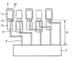
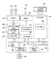
Figure 20 is that expression is as an example that is provided with according to the system of lcd driver of the present invention, the calcspar of the whole configuration of a portable phone.
This routine portable phone comprises a LCD viewing area (liquid crystal display area) 103 as display unit, an antenna that is used to transmit and receive 310, a loud speaker 320 that is used for voice output, a solid-state image pick device 340 that for example constitutes by CCD (charge coupled device) or mos sensor, one for example is made of DSP (digital signal processor), image-signal processor 230 that the picture signal that provides from solid-state image pick device 340 is handled is provided, one according to the lcd driver 104 as the liquid crystal display driving governor of the present invention, a sound interface 241 that is used for input and output signal about loud speaker 320 and microphone 330, a high frequency interface 242 that between it and antenna 310, is used for input and output signal, a baseband portion 250 that is fit to voice signal and transmitting/receiving signal execution signal processing etc., one for example by having the multimedia processing capacity, for example, moving frame according to MPEG (Motion Picture Experts Group) method is handled, the application processor that microprocessor constituted 260 of resolution adjustment function and Java high speed processing function, a memory 281 and 282 that is used for the IC 270 of power supply and is used for storage.
Application processor 260 also has a kind of function, that is, and and except that the picture signal that provides from solid-state image pick device 340, also to handling from the moving frame data that another portable phone receives by high frequency interface 242.Liquid-crystal controller driver 104, baseband portion 250, application processor 260, memory 281,282 and imaging signal processing circuit 230 link together, and transmit data so that allow by system bus 291.In portable telephone system shown in Figure 20, except that system bus 291, also be provided with display data bus 292, and liquid-crystal controller driver 104, application processor 260 and memory 281 are connected with display data bus 292.
Baseband portion 250 is made of an audio signal processor 251,252 and microcomputers of ASIC (application-specific integrated circuit (ASIC)) 253.Audio signal processor 251 for example is made of a DSP (digital signal processor), and is fit to carry out sound signal processing.ASIC 252 provides customization function (user logic).Microcomputer 253 produces baseband signal as a system controller, carries out to show control, and the control whole system.
In memory 281,282, memory 281 is volatile memory that are made of SRAM or SDRAM usually, and for example as a frame buffer, wherein stores the view data that produces from various image processing.Memory 282 is nonvolatile memories, and for example can be at every turn constitutes with the flash memory of predetermined block cell erasure by one.Memory 282 is used to store control program and the control data to whole portable telephone system, comprises display control.
In the system that uses such lcd driver, can wherein arrange display pixel the colored TFT display panels of a dot matrix type as liquid crystal display area 103 by matrix shape.In addition, have in liquid crystal display area 103 under the situation of two TFT liquid crystal panels, also can drive it by single lcd driver.
For example, relevant with the area that reduces semiconductor chip in the semiconductor device as lcd driver with the many export structures of acquisition, provide description hereinafter with reference to Figure 15 to Figure 19 about the content that the inventor has done research.
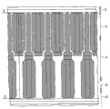
Figure 15 (a) and Figure 15 (b) are the plane graphs that schematically illustrates LCD panel (display panels) 101 separately.Figure 16 is the plane graph that schematically illustrates lcd driver 104.Figure 17 is the plane graph that schematically illustrates the major part of lcd driver 104.Figure 18 is the plane graph that is connected that schematically illustrates internal circuit 108 and protection component 118,119, and electrode pad 110 is arranged with zigzag.Figure 19 is the plane graph that is connected that schematically illustrates internal circuit 108 and protection component 118,119, wherein makes electrode pad 110 with linear array.
As shown in figure 15, LCD panel 101 comprises that is arranged in a substrate 102, for example 103, one of the LCD viewing areas on the glass substrate are arranged near the LCD viewing area 103 lcd driver 104 and the (not shown) backlight as light source on dorsal part that is arranged in LCD viewing area 103.In LCD viewing area 103, on substrate 102, arrange and be used for a plurality of pixels of display screen, so that be positioned at (not shown) on the crosspoint of pixel selection gate line and source electrode line respectively with matrix shape.In addition, on substrate 102, form many substrate wirings 105, so that gate line and source electrode line are electrically connected with the projection (outside lead-out terminal) of lcd driver 104.Therefore, the output signal that provides from lcd driver 104 makes the pixel in the LCD viewing area 103 be changed to ON or OFF by substrate wiring 105.
Pass through the research about the size that reduces the LCD panel, the inventor has found following problem first.
More particularly, as in Figure 15 (a) and Figure 15 (b) with shown in the manner of comparison like that, if make the size of LCD panel 101, promptly the size of substrate 102 reduces, even the size of LCD viewing area 103 remains unchanged, the chip area of the lcd driver 104 that is generally planar rectangular is reduced.And, shown in Figure 15 (b), because lcd driver 104 be arranged near and along LCD viewing area 103, so from reducing the viewpoint of chip area, effectively, draw all outputs from the long limit of the lcd driver 104 that is positioned at LCD viewing area 103, just, adopt so-called monolateral output, and do not draw output from the minor face of lcd driver 104.Just, on the long limit in four limits of lcd driver 104 electrode pad 110 is set, and on minor face, is not provided with.Therefore, shown in Figure 15 (b), the long limit of lcd driver 104 becomes longer, and its minor face becomes shorter, makes the flat shape of lcd driver 104 be tending towards becoming thinner, and can realize reducing of chip area that promptly the LCD panel reduces.
Yet, as will be described in detail, the problem that many export structures bring on the long limit of lcd driver 104 appears.
As shown in figure 16, the lcd driver 104 that is generally planar rectangular comprises input side internal circuit 107 and outlet side internal circuit 108, for example comprises MIS transistor and diode, and they form on the Semiconductor substrate 106 of a formation semiconductor chip.By a plurality of electrode pads 109 that are used to import that are electrically connected with internal circuit 107, from the outside to internal circuit 107 input signals.On the other hand, by a plurality of electrode pads 110 that are used to export that are electrically connected with internal circuit 108, will be from the output signal output of internal circuit 108.The internal circuit 108 that is arranged in the right and the left side is the output circuits that are used for the transistorized grid of LCD panel 101 TFT, and the internal circuit 108 of central authorities is the output circuits that are used for the transistorized source electrode of TFT.On Semiconductor substrate 106, form many signal line 111, so that internal circuit 108 and electrode pad 110 are electrically connected mutually.The holding wire zone that label 112 indications are taken by holding wire 111 on Semiconductor substrate 106.
For example, as shown in figure 17, the electrode pad 110 that is used for the output of lcd driver 104 is arranged with zigzag by two row along the chip of lcd driver 104 is distolateral.In Figure 17; label 113 indication scribe area; be used for being partitioned into each semiconductor chip from semiconductor wafer; label 114 and 115 indicator elment zones; wherein form the protection component (not shown), label 116 indicator elment zones wherein form internal circuit 108; and label 117 indicator elment area of isolation, be used to make between element area 115 and 116 insulation and separate.For example, two protection components are set between power supply internal circuit 108 and GND internal circuit 108, are used for electrostatic protection.
Holding wire 111 shown in Figure 16 is formed on 117 tops, element separation zone.Therefore, in Figure 17, holding wire shown in Figure 16 zone 112 and element separation zone 117 are represented with overlap condition.
Just, as shown in figure 17,, arrange scribe area 113, element area 114, element area 115, element separation zone 117 and element area 116 by order from die terminals side direction chip center side.
In Figure 18, express a kind of state, the electrode pad 110 that wherein is used to export is arranged with zigzag, and protection component 118 and 119 is electrically connected with an internal circuit 108. Protection component 118 and 119 is electrically connected by wiring 120.Internal circuit 108 and protection component 119 are electrically connected by holding wire 111.More particularly, an end of holding wire 111 is drawn from protection component 119, and its opposite end is electrically connected with internal circuit 108.Thereby, draw and the holding wire 111 shared zones that are connected with internal circuit 108 are holding wire zones 112 from protection component 119.
In Figure 19, the electrode pad 110 that is used to export is with linear array, but as the situation of above zigzag layout, an end of holding wire 111 is drawn from protection component 119, and its opposite end is electrically connected with internal circuit 108.
As discussed previously, the pixel on the LCDs is arranged with matrix shape in liquid crystal display area, so that be positioned at respectively on the crosspoint of pixel selection gate line and source electrode line.Therefore, along with the resolution of LCDs becomes higher, pixel selection gate line and source electrode line number also increase, and just, increase to the electrode pad that is used to export 110 numbers that gate line and source electrode line provide from lcd driver 104.
And, because must guarantee the bond strength and the bonding precision of requirement, and satisfy the standard that is applied to as the LCD panel 101 of chip installation side, so reduce to compare, can not make the size of each electrode pad 110 less with the size of holding wire 111 grades.For this reason, depending on circumstances, chip area is determined by the electrode pad number.
In addition, as shown in figure 16, in order to form projection, must arrange the electrode pad that is used to export 110 with spacing P1 as the basis of projection as the outside lead-out terminal of lcd driver 104.Therefore, the spacing P1 of the electrode pad 110 that is used to export is bigger than the spacing P2 of the holding wire 111 on internal circuit 108 sides, and in this side, holding wire is electrically connected with electrode pad 110.As a result of, the holding wire zone 112 that is taken by holding wire 111 also becomes bigger.
Just, when reducing the chip area of lcd driver 104, such problem appears, the number that promptly is positioned at the electrode pad that is used to export 110 on the long limit of lcd driver 104 increases, not only bring the number of holding wire 111 to increase, and bring the size in holding wire zone 112 to increase, and the increase of chip area.
(first embodiment)
Referring to figs. 1 through Figure 11, below put up with according to being applied to the semiconductor device of the first embodiment of the present invention of lcd driver, provide description, it is required the reducing and many export structures of area of semiconductor chip.
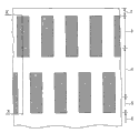
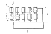
Fig. 1 is the plane graph that schematically illustrates with the major part of 1 semiconductor device of indicating.In same figure also with the perspective state representation electrode pad 9.
On the first type surface of the semiconductor chip of semiconductor device 1, by arrange scribe area 2, element area 3, element area 4, element separation zone 5 and element area 6 from the order of die terminals side direction chip center side (along the vertical direction Fig. 1).
Element area 6 is zones that wherein form the internal circuit 7 that for example comprises MIS transistor and diode.Element separation zone 5 is zones that wherein for example form LOCOS (local oxidation of silicon), is used to insulate and isolate the zone that for example wherein forms element as the MIS transistor.Such a case is arranged sometimes, be not also to form LOCOS in the zone in element separation zone 5 at one wherein, but in the present embodiment, element separation zone 5 is appointed as in the zone between element area 4 and 6.Can use the groove or the ditch type area of isolation that are called SGI (shallow-trench isolation) or STI (shallow isolating trough), form element separation zone 5.For example, by dielectric film of deposition in the ditch that forms in Semiconductor substrate, for example oxide-film or nitride film form STI.Will describe in detail as the back, holding wire 8 is crossed (passover) element separation zone 5, and holding wire 8 is arranged between internal circuit 7 and the electrode pad 9, so that both are electrically connected mutually.
Scribe area 2 is zones that are used for cutting out from semiconductor wafer semiconductor chip.Element area 3 and 4 is the zones that wherein form protection component, exempts from electrostatic influence with protection internal circuit 7, and prevents for example electrostatic breakdown of the transistorized gate insulating film of MIS thus.
Electrode pad 9 is arranged with zigzag along distolateral two row of pressing of the chip of semiconductor device 1.In the present embodiment, electrode pad 9 is arranged on element area 3,4, element separation zone 5 and the element area 6.By holding wire 8, circuit 7 is to electrode pad 9 output signals internally.
With 10 the indication the holding wire zones be one on the semiconductor chip of semiconductor device 1 by holding wire 8 region occupied, its holding wire is electrically connected internal circuit 7 and electrode pad 9 mutually.Fig. 1 represents such a case, and wherein stretch out from the element area 6 that wherein forms internal circuit 7 in holding wire zone 10, then by element separation zone 5, and further to the part of element area 4.
To and begin to locate to Fig. 1 now to do one relatively between Figure 17 of reference in this detailed description of the present invention.Suppose among Fig. 1 from the die terminals to the element area 6 size and from the die terminals to the element area 116 size (along the size of Fig. 1 and Figure 17 vertical direction shown in separately) almost consistent, then the size in the holding wire zone 10 that is taken by holding wire 8 is bigger than the size in the holding wire zone 112 that is taken by holding wire 111.In other words, the number of holding wire 8 shown in Figure 1 is bigger than the number of holding wire shown in Figure 17 111.This shows can increase the number of holding wire 8, and not enlarge its chip area in semiconductor device shown in Figure 11.
Fig. 2 is the plane graph that schematically illustrates the connection of the major part in the semiconductor device shown in Figure 11, also with the perspective state representation electrode pad 9.
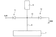
The protection component that label 11 indications form in element area shown in Figure 13, and the protection component of label 12 indication formation in element area shown in Figure 14.Label 13 indication wirings are used for protection component 11 and 12 is electrically connected mutually.As shown in Figure 2, holding wire 8 each comfortable one end are electrically connected with internal circuit 7, and are connected with an output port 29 in its opposite end.Fig. 3 is the connection diagrammatic sketch of the connection of the major part in the expression semiconductor device 1 shown in Figure 2.Fig. 3 represents a kind of for example with the situation of diode as protection component 11 and 12.
As shown in Figure 3, internal circuit 7 and electrode pad 9 are electrically connected, and output to the electrode pad 9 that is used to export by holding wire 8 from the signal of internal circuit 7.The protection component 11 and 12 that is used to protect internal circuit 7 to exempt from electrostatic breakdown is connected electrically between internal circuit 7 and each electrode pad 9, and is electrically connected with mains side and GND side respectively.
To do one relatively between the Figure 18 to Fig. 2 and previous reference now.Fig. 2 has represented the holding wire zone 10 that taken by holding wire 8, and has represented the holding wire zone 112 that taken by holding wire 111 in Figure 18.In Figure 18, the holding wire 111 that stretches out of circuit 108 is connected with internal circuit 108 sides of protection component 118 internally, and the holding wire zone 112 that is therefore taken by holding wire 111 neither crosses protection component 118, does not also cross protection component 119.On the other hand, in Fig. 2, the holding wire 8 that stretches out of circuit 7 is connected with wiring 13 between correlation protection element 11 and 12 separately internally, and protection component 12 is crossed in the holding wire zone 10 that is therefore taken by holding wire 8.,, can increase the number of holding wire 8, and not enlarge the chip area of semiconductor device 1 in conjunction with as described in Fig. 1 as above by signalization line zone 10 above protection component 12.
Thereby; because being used for protection component 11,12 is to draw from the wiring between protection component 11 and 12 13 with the holding wire that is electrically connected 8 between the internal circuit 7; can above protection component 12, arrange holding wire 8 so become; even if make the holding wire number increase, also do not need to increase chip area.Just, because the holding wire zone 10 that is taken by holding wire 8 is set above protection component 12, so needn't increase chip area.
Therefore, under the identical condition of holding wire number,, can reduce the wiring zone on the first type surface of semiconductor chip, particularly have the holding wire zone that takies within the semiconductor chip first type surface of lcd driver of many export structures by using the present invention.
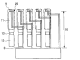
The parts that are positioned in now will the semiconductor device 1 with regard to present embodiment below the electrode pad 9 provide following description.Fig. 4 is the plane graph that schematically illustrates the major part of semiconductor device shown in Figure 11, and electrode pad 9 is with the perspective state representation.
Label 9a among Fig. 4 and 9b indication are positioned at along the chip of semiconductor device 1 distolateral by the electrode pad of two row with the inboard (along under the vertical direction among Fig. 4) of the electrode pad of zigzag arrangement.Electrode pad 9a and 9b are used to export the signal from internal circuit 7.On the other hand, label 9c and 9d indication is positioned at along the chip of semiconductor device 1 distolateral by the electrode pad of two row with the outside (along on the vertical direction among Fig. 4) of the electrode pad of zigzag arrangement.Electrode pad 9c and 9d also are arranged to be used to export the signal from internal circuit 7.Holding wire 8 circuit 7 is internally progressively arranged to above-mentioned output port 29.This is because wire distribution distance in the internal circuit 7 and the interval between the adjacent electrode pad 9 are different mutually, and the latter is bigger.
Any one illusory line that is not electrically connected (dummy line) in label 14 indication and internal circuit 7 and the protection component 11,12.In Fig. 4, illusory line 14 is positioned at below electrode pad 9b and the 9d.Be positioned at periphery sides as the semiconductor device 1 of lcd driver below the electrode pad 9 of part, the number of the holding wire 8 of number ratio below the electrode pad 9 of the middle body of lcd driver of holding wire 8 is little, so be positioned at the wiring occupancy step-down of periphery sides along electrode pad 9 belows of part.Therefore, arrange illusory line 14, so that the wiring occupancy is even.
The illusory line zone that on the semiconductor chip of semiconductor device 1, takies of one of region representation by 15 indications by illusory line 14.Relatively expression between holding wire zone 10 and the illusory line zone 15, the number of the illusory line 14 in the holding wire zone 10 is bigger than the number of the illusory line 14 in the illusory line zone 15.In other words, the periphery sides that is arranged in lcd driver 104 is bigger than the number of the illusory line 14 of the middle body that is arranged in lcd driver 104 (on the left of among Fig. 4) along the number of the illusory line of part (right side among Fig. 4).
Be used for the power supply of internal circuit 7 grades and GND line and be arranged in electrode pad 9c and 9d below, but expression in the drawings, because the description here is at holding wire below electrode pad 9a and 9b 8 and illusory line 4 respectively.
As mentioned above, the output port 29 from the wiring 13 that forms between protection component 11 and 12 is drawn holding wire 8, so that protection component 11 and 12 is electrically connected with internal circuit 7, holding wire 8 can be arranged in protection component 12 tops thus.Therefore, below electrode pad 9a, there are many signal line 8.In this case, the wiring of the holding wire by making electrode pad 9a arranged beneath takies evenly, and the upper surface of electrode pad 9a is almost flushed mutually, just, can improve the Pingdu of the upper surface of electrode pad 9a.And, almost flush mutually by the upper surface that makes electrode pad 9a, the top that joins the projection on it to is almost flushed mutually.
In the present embodiment, take when almost equal when being described as wiring, with the scope within 10%, more preferably the scope within 5% is identified as the error in the manufacture process, and is expressed as wiring and takies evenly.Form the wiring of each electrode pad 9 below, make below each electrode pad and in each wiring layer, it is 50% or more that its wiring takies.
Form illusory line 14, so that the wiring in the zone of electrode pad 9 belows takies evenly.Thereby, below electrode pad 9b, there are many illusory lines 14, and therefore, the wiring of the wiring by making electrode pad 9b arranged beneath takies evenly, and the upper surface of electrode pad 9b is almost flushed mutually.And, almost flush mutually by the upper surface that makes electrode pad 9b, the top that joins the projection on it to is almost flushed mutually.Be arranged to be used to make the wiring in electrode pad 9 lower zones to take uniform illusory line 14, can replenish zone into electrode pad 9d below.
Thereby, because the upper surface Pingdu of the electrode pad 9 that forms on the semiconductor chip of semiconductor device 1 is good, so can be not cause the satisfactory way of any inconvenience, by projection, the projection that forms respectively on a plurality of electrode pads 9 (9a to 9d) and the encapsulation of semiconductor chip are linked together.
Secondly, the structure of putting up with according to the major part of the semiconductor device 1 of present embodiment provides description.Fig. 5 is a plane graph, schematically illustrates the major part of the semiconductor device 1 among Fig. 4, more specifically, is illustrated near the electrode pad 9 of the distolateral location, the electrode pad outside (along on the vertical direction among Fig. 4) of arranging with zigzag by two row of chip.Fig. 6 is the sectional view of being got along the X-X ' line among Fig. 5.In Fig. 5, in order to represent the layout relationship between the wiring layer M1 to M4, not to wiring layer M1 and M4 hatching, but to wiring layer M2 and M3 hatching.In Fig. 5, to a diffusion layer 23 also hatching.In addition, projection 16 shown in Figure 6 is not represented in Fig. 5.Yet, below projection 16, be formed with the semiconductor element pn junction diode of protection component 11 and 12 (for example, as) of wiring layer M1 to M4 and expectation.
Semiconductor substrate 21 for example is made of p type list silicon (Si) crystal, and the device in its first type surface forms on the surface, is formed with element separation zone 22 and diffusion layer adjacent thereto 23.Silica (for example, the SiO that element separation zone 22 each freedom for example use LOCOS (local oxidation of silicon) method to form
2) the film formation.Element separation zone 22 can be by flute profile or ditch shape (SGI: shallow-trench isolation, or STI: shallow isolating trough) form.
On the first type surface of Semiconductor substrate 21, be formed with an internal circuit (not shown), for example comprise the MIS transistor, and the protection component 11 and 12 that for example constitutes by the pn junction diode.Pn junction diode as protection component 11 and 12 is used to prevent electrostatic breakdown, and by the n type of Semiconductor substrate 21 or p type trap 24 and on the p type or the knot of the pn between the n type diffusion layer 23 that cover form.
Above internal circuit and protection component 11 and 12, be formed with wiring layer M1 to M4, they are by interlayer dielectric 25 mutually insulateds and separating.Wiring layer M1 to M4 for example uses aluminium (or aluminium alloy) to form as main component, but can be with the wiring layer of copper (or copper alloy) as embedding (damascene) structure of main component formation.By comprising the conducting film of copper, and be embedded in the groove that forms within the interlayer film of arranging between the adjacent wire layer, make each self-forming of wiring layer of embedded structure as main component.
Wiring layer M1 is by contact hole H1, and internal circuit below being positioned at wiring layer M1 and protection component 11,12 are electrically connected.Wiring layer M2 is by contact hole H2, and M1 is electrically connected with wiring layer.Wiring layer M3 is by contact hole H3, and M2 is electrically connected with wiring layer.In addition, wiring layer M4 is by contact hole H4, and M3 is electrically connected with wiring layer.
Electrode pad 9 is made of wiring layer M4.Similarly, wiring 8 is made of wiring layer M2 and M3.In addition, wiring 13 is made of wiring layer M1.Projection 16 goes up the metal base film 26 that forms by wiring layer M4 (electrode pad 9) and joins wiring layer M4 to.Metal base film 26 has the function of adhering to of improving 16 pairs of electrode pads 9 of projection and interlayer dielectric 25.For example, metal base film 26 is by single high melting point metal film, for example titanium (Ti) or titanium tungsten (TiW) film, or one constitute nickel (Ni) film and gold (Au) film from top to bottom by the stacked film that such order is layered on the titanium film.Projection 16 for example forms by the galvanoplastic of using gold (Au).
As shown in Figure 5 and Figure 6, semiconductor device 1 comprises a holding wire zone 10 that is taken by holding wire 8 and a power line zone 28 that is taken by power line 27 on first type surface on the first type surface of Semiconductor substrate 21.
Holding wire 8 and power line 27 are made of wiring layer M2 and M3.The electrode pad 9 that is electrically connected with projection 16 as outside lead-out terminal is made of the wiring layer M4 that covers above the wiring layer M3.In addition, the wirings 13 that protection component 11 and 12 mutually is electrically connected are made of the wiring layer M1 that is positioned at below the wiring layer M2.
The holding wire 8 that internal circuit from the first type surface that is formed on semiconductor device 1 stretches out is crossed protection component 12, and by contact hole H2 and H3 in the output port 29 that forms in wiring 13, is electrically connected with wiring 13.In addition, wiring 13 is electrically connected with electrode pad 9 by contact hole H2, H3 and H4.Signal from internal circuit outputs to the outside by these connections.
On the other hand, in order to prevent from for example to be applied to the puncture of the caused internal circuit of static on the internal circuit,, between internal circuit and electrode pad 9, be electrically connected protection component 11 and 12 for example in order to prevent the puncture of the transistorized gate insulating film of MIS from the outside.
As shown in Figure 6, in the wiring 13 that approximately is positioned between protection component 11 and 12, output port 29 is set, is used for drawing each holding wire 8 from correlation protection element 11 and 12.Thereby, form therein above the zone of protection component 11 and 12, constituting one can be as the zone in holding wire zone 10.According to prior art, for example, under the situation of the output port 29 that each holding wire 8 is set in the wiring 13 that is arranged in internal circuit side (along Fig. 6 horizontal left side), about holding wire zone 10, holding wire 8 is not arranged on protection component 11 tops.Yet, in a semiconductor device, wherein expanded (develop) a large amount of outputs from internal circuit as the lcd driver, the size increase that is increased caused holding wire zone 10 by the holding wire number has applied considerable influence to chip area.Therefore; by adopting such structure; wherein approximately be positioned in two wirings between the protection component; output port 29 is set; to draw each holding wire from correlation protection element 11 and 12; then becoming can be above protection component 12, and further so far also as above the protection component 11 in holding wire zone 10, arrange holding wire 8.Therefore, even holding wire zone 10 becomes bigger, also can avoid the increase of chip area.In other words; by approximately being positioned in two wirings 13 between the protection component; setting is from the holding wire output port 29 of protection component 11 and 12; become and holding wire 8 also can be arranged in so far also not as in the zone below the electrode pad 9 in holding wire zone 10; so even holding wire zone 10 becomes bigger, also can avoid the increase of chip area.In addition, under situation about holding wire 8 being arranged in below the electrode pad 9, the wiring of the wiring by making electrode pad 9 arranged beneath takies evenly, and the upper surface that can make electrode pad 9 just, can improve their Pingdu mutually near flushing.In addition, flush by the upper surface that makes electrode pad 9 is approaching mutually, the top that can make the projection 16 that joins on it is mutually near flushing.
Secondly, the example about the manufacture process of semiconductor device below provides a description.Fig. 7 to Figure 11 is the plane graph that schematically illustrates the major part of semiconductor device in the manufacture process.The sectional view of the Fig. 6 that is got along X-X ' line among Fig. 5, corresponding with the sectional view that X-X ' line in Fig. 7 to Figure 11 is got.
At first; as shown in Figure 6, on the first type surface of Semiconductor substrate 21, for example form element separation zone 22 by the LOCOS method; form internal circuit (not shown) and protection component 11 and 12 subsequently, wherein this Semiconductor substrate 21 constitutes the semiconductor wafer with basic planar rondure.
Subsequently, on the first type surface of Semiconductor substrate 21, deposit a dielectric film, and, form contact hole H1 in the precalculated position of dielectric film then by photoetching or dry etch technique by CVD (chemical vapour deposition (CVD)).
Subsequently, for example by sputter, on dielectric film, deposit for example titanium nitride film, titanium film, aluminium film and titanium nitride film from top to bottom successively.By photoetching or dry etch technique, make stacked like this metal film experience composition, then to form wiring layer M1.Fig. 7 is the plane graph that schematically illustrates wiring layer M1.Just, the wiring layer M1 of protection component 11 and 12 is crossed in formation in element area 3 and 4.
Similarly, in interlayer dielectric 25, form contact hole H2 then, and on interlayer dielectric 25, form wiring layer M2.Fig. 8 is the plane graph that schematically illustrates wiring layer M2.Just, in element area 3, form the power line 27 of crossing protection component 11, and in element area 4 and 5, form the holding wire 8 of crossing protection component 12.As above described about Fig. 4, circuit 7 is arranged holding wire 8 step by step to output port 29 internally.Depending on circumstances, as above described about Fig. 4, form illusory line 14.
Similarly, in interlayer dielectric 25, form contact hole H3 then, and on interlayer dielectric 25, form wiring layer M3.Fig. 9 is the plane graph that schematically illustrates wiring layer M3.Just, in element area 3, form the power line 27 of crossing protection component 11, and in element area 4 and 5, form the holding wire 8 of crossing protection component 12.As above described about Fig. 4, circuit 7 is arranged holding wire 8 step by step to output port 29 internally.Depending on circumstances, as above described about Fig. 4, form illusory line 14.
Similarly, in interlayer dielectric 25, form contact hole H4 then, and on interlayer dielectric 25, form wiring layer M4.Figure 10 is the plane graph that schematically illustrates wiring layer M4.Just, in element area 3,4 and element separation zone 5, form the wiring layer M4 that comprises electrode pad 9.Wiring layer M1 to M3 and be positioned at below the electrode pad 9 as the protection component 11 and 12 of semiconductor element, and the wiring below the electrode pad in wiring layer M1 to M3 9 takies equal.Form wiring, so that the wiring below each electrode pad 9 takies equal.
Subsequently, deposition is used for the interlayer dielectric 25 of surface protection, forms the hole then, and it is partly exposed wiring layer M4, and forms electrode pad 9.Figure 11 is the plane graph that schematically illustrates electrode pad.
Secondly, for example by sputter, electrically conductive film of deposition on interlayer dielectric 25 such as single high melting point metal film, for example titanium film or titanium tungsten film, perhaps one by stacking gradually the stacked film that nickel film and golden film form from top to bottom on titanium film, and on electrically conductive film, form a photoresist figure, expose, and cover zone in addition so that projection forms the zone.
Then, for example form projection 16, remove the photoresist figure subsequently, and remove electrically conductive film by etching subsequently, to form metal base film 26 as basement membrane by the spraying plating of using gold.Finish the semiconductor device 1 that on electrode pad 9, has projection 16 like this.
(second embodiment)
Formerly among first embodiment, as shown in Figure 2, be arranged with in the semiconductor device of electrode pad 9 with zigzag by two row, between protection component 11 and 12, be provided for the output port 29 of holding wire 8 distolateral along chip.In this second embodiment, will provide description with regard to a kind of semiconductor device that wherein on chip is distolateral, is formed for the output port of holding wire 8.
Figure 12 is the plane graph that schematically illustrates according to the connection of the major part in the semiconductor device of this second embodiment, and wherein electrode pad 9 is with the perspective state representation.
As shown in figure 12; chip at protection component 11 distolateral (along the upside of vertical direction among Figure 12); be formed for the output port 29 of holding wire 8; holding wire 8 provides from protection component 11 and 12 electrical connections to internal circuit 7; holding wire 8 can be arranged in protection component 12 tops thus, and further is arranged in protection component 11 tops.Therefore, even the holding wire number increases, do not need to enlarge chip area yet.More particularly, because a holding wire zone 10 is set above protection component 12 as the shared zone of holding wire 8, so needn't enlarge chip area.
Therefore, under the identical condition of holding wire number,, can reduce the wiring zone on the first type surface of semiconductor chip, particularly have the holding wire zone that takies within the semiconductor chip first type surface of lcd driver of many export structures by using the present invention.
(the 3rd embodiment)
Formerly among first embodiment, as shown in Figure 2, be arranged with in the semiconductor device of electrode pad 9 with zigzag by two row, between protection component 11 and 12, be provided for the output port 29 of holding wire 8 distolateral along chip.In this 3rd embodiment, will provide description along the distolateral semiconductor device of chip with regard to a kind of by delegation's linear array electrode pad 9.
Figure 13 is the plane graph that schematically illustrates according to the connection of the major part in the semiconductor device of this 3rd embodiment, and wherein electrode pad 9 is with the perspective state representation.
As shown in figure 13; even under the situation of the straight line layout of electrode pad 9; also can be from the output port 29 of 13 formation of the wiring between protection component 11 and 12; drawing provides from protection component 11 and 12 holding wires 8 to the electrical connection of internal circuit 7, and can be arranged in protection component 12 tops.Therefore, even the holding wire number increases, do not need to enlarge chip area yet.More particularly, because a holding wire zone 10 is set above protection component 12 as the shared zone of holding wire 8, so needn't enlarge chip area.
Therefore, under the identical condition of holding wire number,, can reduce the wiring zone on the first type surface of semiconductor chip, particularly the holding wire zone that within the semiconductor chip first type surface of lcd driver, takies with many export structures by using the present invention.
(the 4th embodiment)
Formerly among the 3rd embodiment, as shown in figure 13, in the distolateral semiconductor device that electrode pad 9 arranged by delegation's linear array, between protection component 11 and 12, be provided for the output port 29 of holding wire 8 along chip.In this 4th embodiment, below will wherein provide description with regard to a kind of at the distolateral semiconductor device that is formed for the output port 29 of holding wire 8 of chip.
Figure 14 is the plane graph that schematically illustrates according to the connection of the major part in the semiconductor device of this 4th embodiment, and wherein electrode pad 9 is with the perspective state representation.
As shown in figure 14; chip at protection component 11 distolateral (along the upside of vertical direction among Figure 14); be formed for the output port 29 of holding wire 8; provide from protection component 11 and 12 electrical connections to internal circuit 7; holding wire 8 can be arranged in protection component 12 tops thus, and further is arranged in protection component 11 tops.Therefore, even the holding wire number increases, do not need to increase chip area yet.More particularly, because above protection component 12, provide one by the shared holding wire zone 10 of holding wire 8, so needn't increase chip area.
Therefore, under the identical condition of holding wire number,, can reduce the wiring zone on the first type surface of semiconductor chip, particularly have the holding wire zone that takies within the semiconductor chip first type surface of lcd driver of many export structures by using the present invention.
Though abovely described the present invention particularly, much less the invention is not restricted to above embodiment, but under the scope of not violating spirit of the present invention, can carry out various changes by embodiment.
Though the present invention is mainly used in lcd driver in the above description, it belongs to application as background of the present invention, and this is not limited.For example, the present invention also can be applicable to have as SRAM (static RAM) or flash memory (EEPROM: the semiconductor device of the memory circuit Electrically Erasable Read Only Memory), or be applied to a kind of combined semiconductor device that has memory circuit and logical circuit on same substrate.
Though the semiconductor device shown in first embodiment is four layers a wiring substrate, it is not limited, but the present invention also can be applicable to have the semiconductor device of the bigger wiring number of plies.
In addition, though in first embodiment, any one in illusory line and internal circuit and the protection component is not electrically connected, and just, illusory line is whole to be illusory and to be in quick condition, and they can be formed by a part that connects up in the internal circuit.
The present invention can be widely used in semi-conductor industry.