The disclosure that comprise specification, Figure of description and specification digest, is filed in No. 2008-262682nd, the Japanese patent application on October 9th, 2008 is quoted and is incorporated into this by integral body.
Embodiment
If consider and be necessary for facility, can be by each following examples being divided into a plurality of chapters and sections or embodiment describes each embodiment.Yet, unless separately had, clear and definite concrete represent that they are not uncorrelated each other, and they relevant to such an extent as to one of these chapters and sections or embodiment are the modification of some or all other chapters and sections or embodiment or concrete or supplement and describe each other.When quoting (comprising its number, numerical value, quantity and scope) such as component numbers in following examples, unless separately there is clear and definite concrete represent or unless they are obviously limited to concrete number in principle, they are not limited to concrete number.Component numbers etc. can be no less than or no more than concrete number.Unless unless will readily appreciate that in following examples separately by clear and definite concrete represent or to think that in principle it forms (also comprising element, step etc.) obviously indispensable, otherwise that these form is not inevitable indispensable.Similarly, if quote these shapes that form etc., position relationship etc. in following examples, think that shape etc. comprises with it substantially close or similar shape etc., unless unless separately had clear and definite concrete represent or they are obviously really not so in principle.This sets up equally for aforementioned numerical value and scope.
Referring now to accompanying drawing, below embodiments of the invention will be described particularly.Run through the accompanying drawing for illustrated embodiment, the member with identical function will have same numeral, and omit it and be repeated in this description.In following examples, unless be specifically necessary, otherwise in principle by the description not repeating identical or similar portions.
Even if having in the cross-sectional view in accompanying drawing used in an embodiment for illustrative simplicity still can be omitted the situation of hachure.Also there is the situation of can be even adding hachure for plane graph for illustrative simplicity.
(embodiment 1)
The semiconductor device of the present embodiment is described with reference to the accompanying drawings.
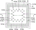
Fig. 1 is the top view (plane graph) as the semiconductor device 1 of one embodiment of the invention.Fig. 2 is the bottom view (basal surface view, back of the body surface view or plane graph) of semiconductor device 1.Fig. 3 is the end view of semiconductor device 1.Fig. 4 is the cross-sectional view (side cross-sectional view) of semiconductor device 1.Cross section along the line A1-A1 of each Fig. 1 and Fig. 2 corresponds essentially to Fig. 4.Fig. 5 is the conceptual plan diagram (top view) of semiconductor chip 2 used in semiconductor device 1.Fig. 6 shows the circuit block diagram of coupled relation between semiconductor chip 2 and outside LSI.Fig. 7 is the conceptual plane perspective view (top view) of semiconductor device 1 when checking semiconductor device 1 through injection molding resin 5.
The semiconductor device 1 of the present embodiment shown in Fig. 1 to Fig. 4 and Fig. 7 is ball grid array (BGA) type semiconductor packages.
As shown in Fig. 2 and Fig. 4, the semiconductor device 1 of the present embodiment comprises wiring board 3, and this wiring board has upper surface (first surface, top surface, first type surface or chip stayed surface) 3a, be formed at a plurality of bonding wires 14 on upper surface 3a, lower surface (second surface, back of the body surface or with the upper surface 3a contrary first type surface) 3b contrary with upper surface and be formed at a plurality of welding zones 16 on second surface 3b.A plurality of welding zones 16 of wiring board 3 comprise and are arranged to multirow and the first welding zone group 56 (the welding zone group corresponding with the first soldered ball group 51) of arranging along the form peripheral edge portions of the lower surface 3b of wiring board 3 and in the lower surface 3b of wiring board 3, are arranged in the first welding zone group 56 with the second welding zone group 57 (the welding zone group corresponding with the second soldered ball group 52) of interior (more approaching the core of the lower surface 3b of wiring board 3 than the first welding zone group 56).In the first welding zone group 56, according to first segment apart from (with the pitch P describing subsequently
1the first corresponding interval) arrange welding zone 16.In the first welding zone group 57, according to than first segment apart from higher second section apart from (with the pitch P describing subsequently
2the second corresponding interval) arrange welding zone 16.
As shown in Figure 4, the semiconductor device 1 of the present embodiment has: semiconductor chip 2; Wiring board 3, for supporting thereon or assembling semiconductor chips 2; A plurality of conductive members 4, are electrically coupled to lip-deep a plurality of electrodes (electrode pad) 2a of semiconductor chip 2 corresponding a plurality of bonding wires 14 with it of wiring board 3; Injection molding resin 5, the upper surface 3a that comprises semiconductor chip 2 and conductive members 4 of covering wiring board 3; And a plurality of soldered balls 6 that provide on the lower surface 3b of wiring board 3.Conductive members 4 in embodiment 1 is the bonding wiring (wiring) that are for example made of gold, thereby below conductive members 4 will be described as to bonding wiring (conductive members) 4.
Below by the description providing the concrete structure of the semiconductor device 1 of the present embodiment.
< semiconductor chip >
First will the structure of semiconductor chip 2 be described.
In forming region such as the corresponding device of the first type surface of the Semiconductor substrate (semiconductor wafer) by being made by monocrystalline silicon etc., form various semiconductor integrated circuit (semiconductor element) SC1 etc., as required polishing semiconductor substrate back of the body surface, then by being cut into small pieces etc., Semiconductor substrate is divided into separately as the independent tube core of individuality of semiconductor chip 2 and obtains semiconductor 2.Semiconductor chip 2 has reciprocal top surface (the 3rd surface or semiconductor element first type surface formed thereon) and back of the body surface (the 4th surface or the first type surface contrary first type surface formed thereon with semiconductor element).It is upper in upper surface (top surface, first type surface or the chip stayed surface) 3a of wiring board 3 that semiconductor chip 2 arranges (assembling), thereby its top surface is towards top (thereby its back side is relative with the upper surface 3a of wiring board 3).The back of the body surface of semiconductor chip 2 is carried out bonding via jointing material (die bonding material, bonding material or adhesive) 8 and is fixed to the upper surface 3a of wiring board 3.As shown in Figure 5, semiconductor chip 2 with the crossing direction of its thickness direction on plan view shape be rectangle, be square in the present embodiment.Semiconductor chip 2 for example has 3 * 10
-6the thermal coefficient of expansion (coefficient of thermal expansion) of/K (or/℃).The size of semiconductor chip 2 (external yardstick) is for example 7mm to 9mm (size is measured as the square of 7mm to 9mm separately).
The example of operable bonding material 8 comprises insulation or conduction cream material etc.As shown in Figure 5, the form peripheral edge portions along the top surface (first type surface) of semiconductor chip 2 forms a plurality of electrodes (electrode pad or bonding welding pad) 2a.Electrode 2a is electrically coupled to semiconductor element or the semiconductor integrated circuit SC1 being formed in semiconductor chip 2 or in its surface layer part via wiring (not shown).Semiconductor chip 2 is arranged at that the upper surface 3a of wiring board 3 is upper and its at least a portion is molded with injection molding resin 5.
Here with reference to Fig. 5 and Fig. 6, provide being formed at the description of coupled relation between semiconductor integrated circuit SC1 on the first type surface of semiconductor chip 2 and a plurality of electrode 2a.
Semiconductor integrated circuit (circuit element) SC1 has: data-signal circuit, for changing from signal (I/O) data of outside LSI supply; Clock circuit, is supplied for data-signal circuit being carried out to the regularly cyclical signal (clock signal or clock pulse) of (synchronously) when the data-signal circuit operation; Addressing circuit, is supplied address signal; Command circuit, is supplied command signal; Electrical source voltage circuit, is supplied for operating the electrical source voltage of these circuit; And reference potential circuit, be supplied reference potential.Outside LSI is arranged in beyond semiconductor device 1 and is represented by label LSI1 and the LSI2 of Fig. 6.For example, semiconductor chip 2 is microcomputer chips.
A plurality of electrodes (electrode pad) 2a comprises electrode 2aSGN1,2aSGN2,2aSGN3,2aSGN4,2aVDD and 2aGND.Electrode (the first electrode) 2aSGN1 is electrically coupled to data-signal circuit to receive from the external interface pad (electrode) of signal (I/O) data of outside LSI1 supply.Electrode (the second electrode) 2aSGN2 is electrically coupled to clock circuit to receive from the external interface pad (electrode) of the clock signal of external devices supply.Electrode (third electrode) 2aSGN3 is electrically coupled to addressing circuit to receive the external interface pad (electrode) of address signal.Electrode (the 4th electrode) 2aSGN4 is electrically coupled to command circuit to receive the external interface pad (electrode) of command signal.Electrode (the 5th electrode) 2aVDD is electrically coupled to electrical source voltage circuit to receive the pad (electrode) of electrical source voltage.Electrode (the 6th electrode) 2aGND is electrically coupled to reference potential circuit to receive the pad (electrode) of reference potential.
That is to say, semiconductor chip 2 has signal electrode (signal electrode pad) 2aSGN1,2aSGN2,2aSGN3 and 2aSGN4, electrical source voltage electrode (electrical source voltage electrode pad) 2aVDD and reference potential electrode (reference potential electrode pad) 2aGND of a plurality of types.Provide a plurality of electrical source voltage electrode 2aVDD and a plurality of reference potential electrode 2aGND, although do not specifically illustrate its respective number.This allows to receive a plurality of electrical source voltages that need for function circuit and allows a plurality of reference potentials to be incorporated in the semiconductor integrated circuit SC1 of semiconductor chip 2.Thereby likely stably operate semiconductor integrated circuit SC1.
< wiring board >
Then will the structure of wiring board 3 be described.
Wiring board (for wiring board or the package substrate encapsulating) 3 as the insert between assembling substrate (motherboard corresponding with the wiring board 31 of describing subsequently) and semiconductor chip 2 has upper surface (first surface) and the conductor layer on lower surface (second surface) (conductive pattern, electrically conductive film pattern or wiring layer) that is injected with the stock layer (dielectric substrate or core material) 11 of insulating resin and is formed at stock layer 11.As shown in Figure 7, wiring board 3 with the crossing plan view shape of thickness direction be rectangle, be square in the present embodiment.The size of wiring board 3 (external yardstick) is for example no less than 12mm (size is measured separately and is about the square of 12mm) in the present embodiment.
Can use conductor layer be wherein formed at the upper surface of single insulating barrier (stock layer 11) and the substrate on lower surface or wherein the MULTILAYER SUBSTRATE (multilayer wiring substrate) of stacked a plurality of insulating barrier (stock layer) and a plurality of conductor layer (wiring layer) as wiring board 3.Also can replace to use and there is flexible membranous type or banding pattern wiring board (band substrate) as wiring board 3.For the stock layer 11 of wiring board 3, can be with as for example for example, by the material the resin material (glass epoxy resin) obtaining to glass fibre resin by injection or organic polymer material.The thermal coefficient of expansion (thermal conductivity) of noting wiring board 3 used in embodiment 1 is greater than the thermal coefficient of expansion (thermal conductivity) of the semiconductor chip 2 of being made by silicon and for example 11 * 10
-6/ K to 13 * 10
-6in this scope of/K.
The upper surface of stock layer 11 and the conductor layer on lower surface are patterned and can be formed by the such conductive material of copper film for example forming by plating method.Conductor layer from the upper surface of stock layer 11, is formed at the upper surface 3a of wiring board 3 for being coupled to a plurality of wiring 15 of a plurality of bonding wires (electrode, bonding welding pad or pad electrode) 14 of bonding wiring 4 and coupling (connection) with it.Bonding wire 14 is parts (although not shown) of wiring 15 and has the width larger than the width of wiring 15.On the other hand, conductor layer from the lower surface of stock layer 11, is formed at lower surface (back of the body surface or the first type surface contrary with the upper surface 3a) 3b of wiring board 3 for being coupled to a plurality of conduction welding zones (electrode, pad or terminal) 16 of soldered ball 6.As required, also likely on the upper surface 3a of wiring board 3 and lower surface 3b, form solder mask layer SR1 and SR2 (not shown in Fig. 4, but illustrated in the Fig. 8 describing later and Fig. 9) (in this case, solder mask layer SR1 is formed on the upper surface 3a of wiring board 3, and solder mask layer SR2 is formed on the lower surface 3b of wiring board 3).
In the present embodiment, as shown in Figure 8, from a corresponding surface of solder mask layer SR1 and SR2 (through its open S R1a and SR2a) exposure bonding wire 14 and welding zone 16, and other conductor layer (such as wiring 15) is covered by solder mask layer SR1 and SR2.Fig. 8 is the amplification cross-sectional view (part amplify cross-sectional view) of region R1 of the dotted line of Fig. 4.Preferably, the respective planes diagram shape of the open S R2a of welding zone 16 and exposure welding zone 16 is circular.
Notice, be different from the structure of Fig. 8, each welding zone 16 also can have the structure that wherein not only exposes as shown in Figure 9 one surface but also expose its side surface.Similar with Fig. 8, Fig. 9 be Fig. 4 dotted line around the amplification cross-sectional view (part amplify cross-sectional view) of region R1.Yet Fig. 9 is corresponding to solder mask layer SR2 is arranged to be greater than this situation of yardstick (diameter) of each welding zone 16 for exposing the yardstick (diameter) of each open S R2a of welding zone 16.As shown in Figure 9, at each welding zone 16, there is in this situation of structure that wherein also exposes its side surface also wet type expansion on the side surface of welding zone 16 of a part for soldered ball 6.Thereby the radius (diameter) that is formed at the soldered ball 6 on welding zone shown in Fig. 9 16 is greater than the radius (diameter) of the soldered ball 6 being formed on welding zone shown in Fig. 8 16.
As shown in Fig. 7 roughly, along being assemblied in the periphery of the semiconductor chip 2 on the upper surface 3a of wiring board 3, each limit along semiconductor chip 2 forms (settings) from a plurality of bonding wires 14 of solder mask layer SR1 exposure.
As shown in Figure 4, bonding wire 14 on the upper surface 3a of wiring board 3 is electrically coupled to the welding zone 16 on its lower surface 3b via wiring 15 and via the wiring (conductor) 18 being formed at as in underpass (through hole), and these paths (through hole) extend towards its lower surface 3b through wiring board 3 from the upper surface 3a of wiring board 3 (its stock layer 11).Therefore, via a plurality of bonding wiring (conductive members) 4 as conductive members, be electrically coupled to a plurality of bonding wires 14 of wiring board 3 with a plurality of electrode 2a of the circuit element SC1 electric coupling of semiconductor chip 2 and via the wiring 15 of wiring board 3, conductor (path wiring 18) in through hole etc., be further electrically coupled to a plurality of welding zones 16 on the lower surface 3b of wiring board 3.
A plurality of welding zones 16 are arranged on the lower surface 3b of wiring board 3 according to array configurations.When specifically describing, as shown in Figure 2, welding zone 16 comprises the first welding zone group 56 that is arranged to multirow and arranges along the form peripheral edge portions (each limit) of the lower surface 3b of wiring board 3, and in the lower surface 3b of wiring board 3, is arranged in the first welding zone group 56 with the second welding zone group 57 of interior (more approaching the core of lower surface (second surface) 3b of wiring board 3 than the first welding zone group 56).
Here, in Fig. 2, the dotted line that label X, Y and Z represent is dummy line.The region of the dotted line that label X represents is corresponding to the region that the first welding zone group 56 (or first soldered ball group 51) is wherein set.The region of the dotted line that label Y represents is corresponding to the region that the second welding zone group 57 (the second soldered ball group 52) is wherein set.The region correspondence of the dotted line that label Z represents wherein arranges the region of calibrating terminal (welding zone) 17.
That is to say, in Fig. 2, the first welding zone group 56 comprises the welding zone 16 in the region that is positioned at dotted line X encirclement.Therefore, the welding zone that belongs to the first welding zone group 56 among welding zone 16 by it, give label 16a be called as welding zone 16a and also the label 16a in Fig. 2 represent.On the other hand, in Fig. 2, the second welding zone group 57 comprises the welding zone 16 in the region that is positioned at dotted line Y encirclement.Therefore, the welding zone that belongs to the second welding zone group 57 among welding zone 16 by it, give label 16b be called as welding zone 16b and also the label 16b in Fig. 2 represent.
At this moment, as shown in Figure 4, the second welding zone group 57 (the welding zone 16b that belongs to this group) be assemblied in semiconductor chip 2 on the upper surface 3a of wiring board 3 substantially in the region of Two-dimensional Overlapping.In the first welding zone group 56, welding zone 16 (being welding zone 16a here) according to first segment apart from (with the pitch P describing subsequently
1the first corresponding interval) arrange.On the other hand, in the second welding zone group 57, welding zone 16 (being welding zone 16b here) according to than first segment apart from higher second section apart from (with the pitch P describing subsequently
2the second corresponding interval) arrange.
Soldered ball (ball electrode, welding block, cube electrode or projection electrode) 6 as outside terminal is coupled to corresponding welding zone 16 (being arranged on corresponding welding zone 16).Thereby a plurality of soldered balls 6 are on the lower surface 3b of wiring board 3, be arranged as welding block according to array configurations the lower surface (first type surface) of semiconductor device 1 is upper.The lower surface with setting soldered ball 6 thereon of semiconductor device 1 (being the lower surface 3b of wiring board 3) is as the assembly surface (first type surface that semiconductor device 1 is fitted thereon on assembling substrate) of semiconductor device 1.The outside terminal that soldered ball 6 is made, carried out work and can be used as semiconductor device 1 as the cube electrode (projection electrode or welding block) of semiconductor device 1 by welding material carrys out work.Soldered ball 6 can be considered as welding block.A plurality of electrode 2a of semiconductor chip 2 are electrically coupled to a plurality of bonding wires 14 of wiring board 3 and a plurality of soldered balls 6 that are further electrically coupled to a plurality of welding zones 16 of wiring board 3 and are coupled to a plurality of welding zones 16 via the wiring 15 of wiring board 3, conductor (path wiring 18) in through hole etc. via a plurality of bonding wiring 4.Can be for release heat with the soldered ball 6 of the electrode 2a electric coupling of semiconductor 2 yet.
Near the core of the lower surface 3b of wiring board 3, (in the position nearer than the second welding zone group 57 and the core of the lower surface 3b of wiring board 3) arranges a plurality of calibrating terminals (welding zone) 17.Attention is in Fig. 2, and calibrating terminal (welding zone) 17 is positioned at the region that dotted line Z surrounds.Each terminal 17 is formed by the welding zone 16 that is not coupled to soldered ball 6.Therefore, being formed at a plurality of welding zones 16 on the lower surface 3b of wiring board 3 comprises and is coupled to the welding zone 16 (being welding zone 16a and 16b) of soldered ball 6 and the welding zone 16 as calibrating terminal 17 that is not coupled to soldered ball 6.
Similar with the welding zone 16 that is coupled to soldered ball 6, calibrating terminal 17 is also via the conductor layer (such as the conductor in through hole, wiring 15 and bonding wire 14) of wiring board 3 and be electrically coupled to the electrode 2a of semiconductor chip 2 via bonding wiring 4.By being applied to terminal 17, probe for testing etc. can test (inspection) semiconductor device 1.After manufacturing semiconductor device 1 and before assembling semiconductor device 1, (before it being for example assembled to the wiring board 31 of describing subsequently) used the test (inspection) of 17 pairs of semiconductor device 1 of terminal.Terminal 17 is the terminals for test (inspection) semiconductor device 1, and therefore after assembling semiconductor device 1, (after it being for example assembled to the wiring board 31 of describing subsequently) do not re-use.Therefore, the terminal 17 of semiconductor device 1 for example, without the terminal (substrate terminal 32 of the wiring board 31 of describing subsequently) that is electrically coupled to the wiring board for semiconductor device 1 is fitted thereon, thereby soldered ball 6 is not coupled to terminal 17.If without calibrating terminal 17, also can omit its formation.
Injection molding resin (injection molding resin part, molding part or molding) 5 is such as by making as the resin material of thermosetting resin material and also can comprising filler etc.For example, also can form injection molding resin 5 with the epoxy resin that comprises filler etc.Injection molding resin 5 is formed at the upper surface 3a of wiring board 3 above to cover semiconductor chip 2 and bonding wiring 4.Molded and protection semiconductor chip 2 and bonding wiring 4 by injection molding resin 5.Note the thermal coefficient of expansion of injection molding resin 5 used in embodiment 1 be less than the thermal coefficient of expansion of wiring board 3, but be greater than the thermal coefficient of expansion of the semiconductor chip 2 of being made by silicon.By forming such injection molding resin 5 on the upper surface 3a at wiring board 3, likely in a certain degree, reduce the expansion/contraction stress that heat treatment step causes due to the difference of semiconductor chip 2 and the thermal coefficient of expansion of wiring board 3.
Therefore, the semiconductor device 1 of the present embodiment shown in Fig. 1 to Fig. 4 and Fig. 7 is that wherein semiconductor chip 2 is assembled on wiring board 3 and soldered ball 6 is bonded to the semiconductor device (semiconductor packages) of wiring board 3 as outside terminal.Semiconductor device 1 is the semiconductor device of this form of following CSP (chip size packages), and this CSP is the approximately small size semiconductor packages equally large or bigger with semiconductor chip 2 of size.The planar configuration of semiconductor device 1 (wiring board 3) can be for example that each limit measurement is about the square of 12mm.Semiconductor device 1 has the soldered ball 6 of arranging according to array configurations and can be used as the semiconductor device that BGA encapsulates this form and carrys out work.
< method, semi-conductor device manufacturing method >
The manufacture method of the semiconductor device 1 of the present embodiment is then described with reference to the accompanying drawings.Figure 10 shows the process chart of the step of the semiconductor device 1 of manufacturing the present embodiment.Figure 11 to Figure 15 and Figure 22 are the semiconductor device 1 of the present embodiment cross-sectional views in its manufacturing step, and each cross-sectional view has illustrated the cross section corresponding with above-mentioned Fig. 4 (along the cross section of the line A1-A1 of above-mentioned Fig. 2).Figure 16 to Figure 21 is the exemplary plot (for the figure of example) of step of soldered ball 6 of being coupled in step S5, and each exemplary plot has illustrated the cross section corresponding with the line B1-B1 of above-mentioned Fig. 2.
In the present embodiment, by the description providing following situation, use in this case the multi-disc wiring board (wiring board motherboard) 21 that wherein forms a plurality of wiring boards 3 according to array configurations with annexation to manufacture individual semiconductor device 1.
First as shown in Figure 11, prepare wiring board (insert) 21 (step S1).Wiring board 21 is motherboards of above-mentioned wiring board 3 and cut to be divided into the individuality independent sheet corresponding with individual semiconductor device region (substrate region or unit substrate region) 22 in the cutting step of describing subsequently.Each semiconductor device region 22 is corresponding to the wiring board 3 of semiconductor device 1.Wiring board 21 has following structure, in this structure, according to matrix shape, arranges a plurality of semiconductor device region 22, wherein from each semiconductor device region 22, forms a semiconductor device.Thereby each semiconductor device region 22 of the upper surface 21a of wiring board 21 is formed with aforesaid bonding wire 14 and wiring 15, and each semiconductor device region 22 of the lower surface 21b of wiring board 21 is formed with aforesaid welding zone 16 and calibrating terminal 17.
Then as shown in Figure 12, by semiconductor chip 2 via bonding material 8 bondings (die bonding or chip assembling) to (step S2) on the corresponding semiconductor device region 22 of the upper surface 21a of wiring board 21.The example of bonding material 8 comprises insulation bonding material, but also can use conduction bonding material, such as silver paste.For example, bonding material 8 is coated to the core substantially in each semiconductor device region 22 of upper surface 21a of wiring board 21 to form chip fixed adhesive layer, semiconductor chip 2 is positioned on jointing material 8, and heats etc. to realize the upper surface 21a of wiring board 21 and via bonding material 8, be bonded to the back of the body surface of semiconductor chip 2.
Then as shown in Figure 13, carry out wiring bonding step the individual electrode 2a of semiconductor chip 2 is electrically coupled to and is correspondingly with it formed at the bonding wire 14 (step S3) on wiring board 21 via bonding wiring 4.That is to say, a plurality of bonding wires 14 on each semiconductor device region 22 of the upper surface 21a of wiring board 21 are electrically coupled to bonding (assembling) to a plurality of electrode 2a of the semiconductor chip 2 on semiconductor device region 22 via a plurality of bonding wiring 4.
After wiring bonding step, as shown in Figure 14, for example, by injection step (transmitting injection step), undertaken resin molded to form injection molding resin 5a (molding part) and molded (resin molded) semiconductor chip 2 and bonding wiring 4 (step S4) with injection molding resin 5a.In molded step, carry out following simultaneously moldedly, this is simultaneously molded with injection molding resin 5 a plurality of semiconductor device region 22 of the upper surface 21a of molded wiring board 21 simultaneously.That is to say, form injection molding resin 5a so that semiconductor chip 2 and the bonding wiring 4 on a plurality of semiconductor device region 22 of the upper surface 21a of covering wiring board 21.For this purpose, form injection molding resin 5a to cover a plurality of semiconductor device region 22 of the upper surface 21a of wiring board 21.Injection molding resin 5a is such as by making and also can comprise filler etc. as resin material of thermosetting resin material etc.The epoxy resin that for example, can comprise filler by use forms injection molding resin 5a.For example, can form injection molding resin 5a by injection molding resin material being expelled in the cavity that is arranged at the injection molding die on wiring board 21 and by the injection molding resin material that is heating and curing.
Then as shown in Figure 15, by soldered ball 6 couplings (bonding) to the welding zone 16 (step S5) on the lower surface 21b of wiring board 21.
With reference to Figure 16 to Figure 21, be described in the example of the step of the soldered ball 6 that is coupled in step S5.
Arranging with the wiring board 21 that injection molding resin 5a forms makes the lower surface 21b of wiring board 21 as shown in Figure 16 towards top.In addition, preparation is as shown in Figure 17 for attracting the mask 24 of soldered ball by suction.Mask 24 has the structure that wherein for example provides a plurality of holes (through hole 24a) in having the member of writing board shape.In mask 24, the layout of a plurality of hole 24a (placement position) is corresponding to the layout (placement position) of the welding zone 16 on the lower surface 21b of wiring board 21 and corresponding to being arranged at the layout of the soldered ball 6 on the lower surface 21b (the lower surface 3b of wiring board 3) of wiring board 21.
Then as shown in Figure 18, the respective aperture 24a by suction, soldered ball 6 being attracted to mask 24.By the diameter of hole 24a being arranged to be less than the diameter of soldered ball 6 and making mask 24 more approach soldered ball 6, through via hole 24a, sucking in external air the respective aperture 24a that can soldered ball 6 be attracted to mask 24 by suction.
Then as shown in Figure 19, will be immersed in flux 25 by aspirating the soldered ball 6 attracting to the respective aperture 24a of mask 24, thereby flux 25 is coated to each soldered ball 6.
Then on the welding zone 16 on the lower surface 21b of wiring board 21, arrange by aspirating to attract the soldered ball 6 of respective aperture 24a as shown in Figure 20.Stopping, after the suction of via hole 24a, from soldered ball 6, pulling open mask 24.Thereby a plurality of soldered balls 6 are arranged on a plurality of welding zones 16 on the lower surface 21b of wiring board 21 and temporarily fixing by flux 25.Subsequently, by carrying out solder reflow process (reflux technique or heat treatment), as heat treatment, carry out melting solder, and again solidified solder to allow bonding soldered ball 6 and soldered ball 6 to be electrically coupled to the welding zone 16 on the lower surface 21b of wiring board 21.Subsequently, also likely carry out as required the lip-deep flux 25 that cleaning and removal are attached to soldered ball 6 etc.Attention does not provide hole 24a in the position corresponding with calibrating terminal 17 in mask 24, so soldered ball 6 is not coupled on calibrating terminal 17, is still coupled on the welding zone 16 except calibrating terminal 17 as shown in above-mentioned Figure 15.
Therefore the soldered ball of the outside terminal as semiconductor device 16 is bonded to the lower surface 21b of wiring board 21 in step S5.The soldered ball 6 that is bonded to the lower surface 21b of wiring board 21 can be considered as welding block (cube electrode).In the present embodiment, provided join the description of welding zone 16 these situations to using soldered ball 6 as the outside terminal of semiconductor device 1, but the invention is not restricted to this.Also likely such as by printing process etc. rather than bonding soldered ball 6, scolder being fed on welding zone 16 and forming thus the welding block (cube electrode) (corresponding to the embodiment 4 describing subsequently) as the outside terminal of semiconductor device 1 on welding zone 16.Material as the outside terminal (being soldered ball 6 here) of semiconductor device 1, can be used one of solder containing pb and lead-free lead-free solder.Yet, when heavily paying close attention to the measure of Preventing Environmental pollution problem, more preferably use the lead-free solder of not leaded (Pb).As the material of lead-free solder, only there is tin (Sn) or tin (Sn) alloy-layer made by tin (Sn)-bismuth (Bi) alloy, tin (Sn)-Yin (Ag)-copper (Cu) alloy etc. is preferred.In the situation that using alloy-layer, can be than in the situation that use the soldered ball only being formed by tin to stop more reliably whisker to form problem.
Then carrying out as required mark gives mark with the surface to injection molding resin 5a, such as production code member (step S6).For example, can carry out carrying out with laser the laser labelling of mark, or also can use China ink to carry out the black mark of mark.Also likely change in step S5, the be coupled step of soldered ball 6 and the order of the markers step in step S6 and the markers step of carrying out thus, the be coupled step of soldered ball 6 then in step S5 in step S6.When not needing, also can omit the markers step in step S6.
Then as shown in Figure 22, (by being cut into small pieces) cutting wiring board 21 becomes individual semiconductor device region 22 (step S7) with the injection molding resin 5a on being formed at it with separated (division).By cutting like this/and individually oriented, can manufacture semiconductor device 1 as shown in above-mentioned Fig. 1 to Fig. 4 and Fig. 7.Wiring board 21 after separated (divisions) becomes individual semiconductor device region 22 is corresponding to wiring board 3, and injection molding resin 5a after separation (division) one-tenth individual semiconductor device region 22 is corresponding to injection molding resin 5.
After manufacturing semiconductor device 1, can to semiconductor device 1, check (test) by calibrating terminal 17 on the lower surface 3b of probe etc. and wiring board 3 is contacted.Can carry out for determining that semiconductor device 1 is for non-faulty goods or the filler test of faulty goods.The semiconductor device 1 that assembling is selected as non-faulty goods on assembling substrate etc. is also used it.Therefore, before the step of the assembling semiconductor device 1 of then describing, carry out the inspection of use test terminal 17.
< semiconductor module manufacture method >
Then describe with reference to the accompanying drawings by manufacture the method for semiconductor module at the semiconductor device 1 of the upper assembling of assembling substrate (motherboard) the present embodiment.Figure 23 shows the process chart of the part steps (step of assembling semiconductor device 1) of manufacturing semiconductor module.Figure 24 is the cross-sectional view (major part cross-sectional view) as the wiring board 31 of the assembling substrate being fitted thereon for semiconductor device 1.Figure 25 is the plane graph (major part plane graph) of wiring board 31.Figure 26 is the part amplification view of Figure 25.Figure 27 is that the part of wiring board 31 is amplified cross-sectional view.Attention corresponds essentially to Figure 24 along the cross-sectional view of the line A2-A2 of Figure 25, and the enlarged drawing in the region 27 that 2 chain type lines of Figure 25 surround corresponds essentially to Figure 26, and corresponds essentially to Figure 27 along the cross section of the line C1-C1 of Figure 26.In order to be easier to understand, Figure 26 shows substrate terminal 32 and the corresponding pattern of drawing wiring 35 when checking through the solder mask layer 36 of wiring board 31.When semiconductor device 1 is assemblied in Semiconductor substrate 31, the A2-A2 line of Figure 25 overlaps with the line A1-A1 of above-mentioned Fig. 1 and Fig. 2 two dimension.In Figure 25, when semiconductor device 1 is assemblied on wiring board 31, the region of semiconductor device 1 Two-dimensional Overlapping (wherein assembling the region of semiconductor device 1) 28 is also illustrated by the broken lines.Figure 28 to Figure 30 is the semiconductor module of the present embodiment cross-sectional view (major part cross-sectional view) in its manufacturing step step of semiconductor device (assembling), and these cross-sectional views have illustrated the cross-sectional view corresponding with above-mentioned Figure 24, the i.e. also cross section corresponding with above-mentioned Fig. 4.Figure 31 is that the part of Figure 30 is amplified cross-sectional view.Figure 30 and Figure 31 show semiconductor device 1 and are assemblied in the state on wiring board 31.Figure 32 and Figure 33 are plane graph and the cross-sectional views that is shown schematically in separately the semiconductor module MJ1 example of manufacture.Cross section along the line D1-D1 of Figure 32 corresponds essentially to Figure 33.
First, using and prepare semiconductor device 1 (step S11) and prepare the wiring board 31 (step S12) as the assembling substrate being fitted thereon for semiconductor device 1 with mode identical in above-mentioned steps S1 to S7.Can in step S11, to the preparation of semiconductor device 1 (manufacture), carry out before, afterwards or with it in step S12 the preparation of wiring board 31 (manufacture) simultaneously.The thermal coefficient of expansion of wiring board 31 (coefficient of thermal expansion) is for example 14 * 10
-6/ K to 16 * 10
-6in this scope of/K.
As shown in Figure 24 to Figure 27, wiring board (assembling substrate or motherboard) 31 has a plurality of substrate terminal (coupling terminal, electrode, pad electrode or conduction welding zone) 32, these substrate terminal are for a plurality of outside terminals (being soldered ball 6 here) of the semiconductor device 1 on individual coupling upper surface (top surface or first type surface) 31a, and this upper surface is as the assembly surface being fitted thereon for semiconductor device 1.Attention shows the cross-sectional structure of wiring board 31 in Figure 24 with simplified way, but wiring board 31 has cross-sectional structure as shown in Figure 27 when specifically describing.
Preferably, the multilayer wiring substrate (MULTILAYER SUBSTRATE) of wiring board 31 a plurality of insulator layers (dielectric layer or insulation stock layer) 33 that be wherein integrally stacked and a plurality of wiring layer (conductor layer or pattern layers) 34.In Figure 27, stacked three insulator layers 33 to be to form wiring board 31, but the number of stacked insulator layer 33 is not limited to this and differently change.
In Figure 27, also on the upper surface 31a of wiring board 31 and between insulator layer 33, form wiring layer 34.Yet if desired also can be at lower surface (back of the body surface) the upper formation of the 31b wiring layer 34 of wiring board 31.The example of material that is used to form the insulator layer 33 of wiring board 31 comprises that ceramic material is as aluminium oxide (alundum (Al2O3) or Al
2o
3), resin material (such as glass epoxy resin) etc.
From wiring board 31, wiring layer 34 most, a plurality of substrate terminal 32 of being made by conductor and be coupled to the drawing on the upper surface 31a that wiring 35 is formed at wiring board 31 of respective substrate terminal 32.Substrate terminal 32 is for being coupled to the soldered ball (cube electrode) 6 as the outside terminal of semiconductor device 1.When semiconductor device 1 was assemblied in the upper surface 31a of wiring board 31 when upper, substrate terminal 32 is arranged at towards the position of soldered ball 6 (with soldered ball 6 Two-dimensional Overlappings).Therefore, a plurality of substrate terminal 32 be formed at wiring board 31 upper surface 31a wherein plan will assembling semiconductor device 1 region on.The layout of the soldered ball 6 of (being on the lower surface 3b of wiring board 3) on the lower surface of the layout of a plurality of substrate terminal 32 corresponding to semiconductor device 1.That is to say, the layout of a plurality of substrate terminal 32 of wiring board 31 (identical with the layout of soldered ball 6) is corresponding to the layout of the soldered ball (cube electrode) 6 of the outside terminal as semiconductor device 1.In addition, if desired, other terminal (terminal except substrate terminal 32) also can be formed among the upper surface 31a of wiring board 31 except wherein the planning on the region the region of assembling semiconductor device 1 of this upper surface, and the electronic unit except semiconductor device 1 etc. also can be fitted thereon.
Draw wiring 35 and the identical wiring layer 34 (wiring board 31 go up most wiring layer 34) of substrate terminal 32 and with it coupling form.That is to say, as shown in Figure 26, substrate terminal 32 is to draw a part for wiring 35 and have the width larger than the width of drawing wiring 35.Drawing wiring 35 can be used as for substrate terminal 32 and the wiring of other terminal coupling of wiring board 31 are carried out to work.In addition, solder mask layer 36 is formed at that the upper surface 31a of wiring board 31 is upper covers other region to expose each substrate terminal 32, and draws wiring 35 and covered by solder mask layer 36.As required, the wiring layer 34 that forms wiring board 31 is via the conductor in the hole (through hole or hole) 37 being formed in insulator layer 33 or via electrically conductive film 38 electric coupling.
Then as shown in Figure 28, by solder cream (scolder or emulsion scolder) 41 supplies (print, give, apply or arrange) to (step S13) in a plurality of substrate terminal 32 of wiring board 31.At this moment, can be for example by using the printing process of solder printing mask (not shown) that solder cream 41 is fed in a plurality of substrate terminal 32 of wiring board 31.
Then on wiring board 31, assemble (setting) semiconductor device 1 (step S14).
In step S14, on wiring board 31, assemble in the step of semiconductor device 1, as shown in Figure 29, semiconductor device 1 is arranged on the upper surface 31a of wiring board 31, thereby the first type surface that wherein forms soldered ball 6 of semiconductor device 1 (being the lower surface 3b of wiring board 3) is towards the first type surface that wherein forms substrate terminal 32 (being the upper surface 31a of wiring board 31) of wiring board 31.At this moment, on the upper surface 31a of wiring board 31, aim at and assembling (setting) semiconductor device 1, thereby a plurality of substrate terminal 32 of wiring board 31 are relative with a plurality of soldered balls 6 of semiconductor device 1 via the scolder (solder cream 41) being fed in step S13 in substrate terminal 32.Thereby the individual soldered ball 6 of semiconductor device 1 is relative with the respective substrate terminal 32 of wiring board 31 via the solder cream 41 providing in each substrate terminal 32 of wiring board 31.So soldered ball 6 and solder cream 41 and substrate terminal 32 Two-dimensional Overlapping substantially at this moment.The bond property of the solder cream 41 in the substrate terminal 32 of wiring board 31 allows the soldered ball 6 of semiconductor device 1 to be temporarily fixed to the substrate terminal 32 of wiring board 31.
After semiconductor device assembling (setting) is on wiring board 31, carry out solder reflow process (reflux technique or heat treatment) as heat treatment (step S15).Figure 30 and Figure 31 show the state after the solder reflow process in step S15.
For example, make the wiring board 31 (structure of Figure 29) that is formed with semiconductor device 1 on it as above through unshowned reflow ovens etc., thereby the scolder heating in reflow ovens (solder cream 41 and soldered ball 6) fusing is to be bonded together the substrate terminal of wiring board 31 32 and the soldered ball 6 of semiconductor device 1.By solder reflow process, the soldered ball of semiconductor device 16 is with to be fed to soldered ball 6 integrated to form soldered ball 46 after assembling semiconductor device 1 by the solder cream in the substrate terminal being coupled to 32 41.As shown in Figure 30 and 31, individual soldered ball 46 bondings of semiconductor device 1 and the respective substrate terminal 32 that is electrically coupled to wiring board 31.That is to say, a plurality of outside terminals of semiconductor device 1 (being soldered ball 6 here) individuality is coupled to a plurality of substrate terminal 32 of wiring board 31.
In this way, semiconductor device 1 assembling (assemble welding), on wiring board 31, is manufactured semiconductor device or the wherein semiconductor device of semiconductor device 1 assembling (loading) on wiring board 31 or semiconductor module (Figure 30 and 31 structure) thus.Thereby semiconductor device 1 is fixed to wiring board 31, and as a plurality of soldered balls 46 (soldered ball 6) of the outside terminal of semiconductor device 1, be electrically coupled to a plurality of substrate terminal 32 of wiring board 31.Thereby a plurality of electrode 2a of semiconductor chip 2 are via the conductor (not shown) in a plurality of bonding wiring 4, a plurality of bonding wires 14 via wiring board 3, wiring 15, through hole and welding zone 16 and be electrically coupled to a plurality of substrate terminal 32 of wiring board 31 via a plurality of soldered balls 46.
After semiconductor device 1 is assembled to the step on wiring board 31, before installation step or in identical installation step, other electronic unit etc. also can assemble (loading) on wiring board 31.In the present embodiment, as shown in Figure 32 and Figure 33, for example capacitor CP1 and resistor RS1 assemble (loading) on the upper surface 31a of wiring board 31 and around semiconductor device 1 as electronic unit (external equipment), thus configuration (manufacture) semiconductor module MJ1.
After solder cream 41 being fed in a plurality of substrate terminal 32 of wiring board 31 in step S13, more preferably carry out step S14 (step of assembling semiconductor device 1) and step S15 (solder reflow step) to contribute to the soldered ball of semiconductor device 16 to be bonded to the substrate terminal 32 of wiring board 31.Yet, also can omit step S13 (step of supply solder cream 41).In the situation that omit step S13 (step of supply solder cream 41), when assembling semiconductor device 1 on assembling substrate 31 in step S14, the individual soldered ball 6 of semiconductor device 1 and no solder paste 41 insertions toward each other and therebetween of the individual substrate terminal 32 of wiring board 31.Then, by carry out solder reflow process and heating and melting soldered ball 6 in step S15, the substrate terminal 32 of wiring board 31 can be bonded to the soldered ball 6 of semiconductor device 1.By solder reflow process melt and again curing soldered ball 6 after the assembling of above-mentioned semiconductor device 1 as soldered ball 46.
The layout > of < welding zone and soldered ball
Then by provide on the lower surface of the semiconductor device 1 at the present embodiment, on the lower surface 3b of wiring board 3, arrange the specific descriptions of the mode of a plurality of soldered balls 6 (or welding zone 16).
The semiconductor device 1 of the present embodiment has a plurality of soldered balls (with welding zone 16) on the lower surface 3b that is arranged in wiring board 3 as shown in above-mentioned Fig. 2.
Because the corresponding welding zone 16 (except calibrating terminal 17) that soldered ball 6 is arranged on the lower surface 3b of wiring board 3 is upper, so the layout of the layout of the lower surface 3b place welding zone 16 (except calibrating terminals 17) of wiring board 3 and the lower surface 3b place soldered ball 6 of wiring board 3 is identical.Therefore in Fig. 2, welding zone 16 is arranged at the two-dimensional position identical with the two-dimensional position of soldered ball 6.That is to say, in Fig. 2, welding zone 16a is arranged at the two-dimensional position identical with the two-dimensional position of soldered ball 6a, and welding zone 16b is arranged at the two-dimensional position identical with the two-dimensional position of soldered ball 6b.
As seen from Figure 2, in the semiconductor device 1 of the present embodiment, a plurality of soldered balls 6 (outside terminal) are divided into a plurality of soldered ball groups (outer end subgroup or welding block group) and (are the first soldered ball group 51 and second soldered ball group 52 these two soldered ball groups (outer end subgroup or welding block group) here and are arranged on the lower surface 3b of wiring board 3.Particularly, a plurality of soldered balls 6 that provide on the lower surface (the lower surface 3b of wiring board 3) of semiconductor device 1 are included in the first soldered ball group (the first outer end subgroup or the first welding block group) 51 that the external peripheral sidepiece of the lower surface 3b of wiring board 3 arranges according to the multirow extending in circulation pattern (being two row) and the second soldered ball group (the second outer end subgroup or the second welding block group) 52 of arranging according to the multirow extending in circulation pattern (being two row) in the inside position of the first soldered ball group 51 here here.
Among a plurality of soldered balls 6, the soldered ball 6 that belongs to the first soldered ball group (the first outer end subgroup or the first welding block group) 51 is called soldered ball 6a by give label 6a to it, and the soldered ball 6 that belongs to the second soldered ball group (the second outer end subgroup or the second welding block group) 52 is called soldered ball 6b by give label 6b to it.
Here, the first soldered ball group 51 comprises that individuality is arranged at a plurality of soldered ball 6a on a plurality of welding zone 16a that comprise the first welding zone group 56, and the second soldered ball group 52 comprises that individuality is arranged at a plurality of soldered ball 6b on a plurality of welding zone 16b that comprise the second welding zone group 57.That is to say, individual on the corresponding welding zone 16a in the first welding zone group 56 the soldered ball 6a in the first soldered ball group 51 is set, and individual on corresponding welding zone 16b in the second welding zone group 57 the soldered ball 6b in the second soldered ball group 52 is set.Lower surface 3b at wiring board 3, the mode that welding zone 16a in the first welding zone group 56 arranges is identical with the mode that the soldered ball 6a in the first soldered ball group 51 arranges, and the mode that welding zone 16b in the second welding zone group 57 arranges is identical with the mode of soldered ball 6b layout in the second soldered ball group 52.On the other hand, at the lower surface 3b of wiring board 3, the first welding zone group 56 is identical with the position relationship between the first soldered ball group 51 and the second soldered ball group 52 with the position relationship between the second welding zone group 57.
As mentioned above, a plurality of welding zones 16 on the lower surface 3b of wiring board 3 comprise: the first welding zone group 56, and wherein according to multirow, arrange and arrange welding zone 16 (being welding zone 16a) along the form peripheral edge portions of the lower surface 3b of wiring board 3; And the second welding zone group 57, wherein welding zone 16 (being welding zone 16b) is arranged in the first welding zone group 56 in the lower surface 3b of wiring board 3.Thereby a plurality of soldered balls 6 on the lower surface 3b of wiring board 3 (being outside terminal) comprising: the first soldered ball group 51, wherein according to multirow, arrange and along the form peripheral edge portions solder ball placement (being soldered ball 6a) of the lower surface 3b of wiring board 3; And the second soldered ball group 52, wherein soldered ball 6 (being soldered ball 6b) is arranged in the first soldered ball group 51 on the lower surface 3b of wiring board 3.That is to say, as mentioned above, on the corresponding welding zone 16a in the first welding zone group 56 of arranging according to multirow along the form peripheral edge portions (each limit) of the lower surface 3b of wiring board 3, provide the soldered ball 6a in the first soldered ball group 51.On the other hand, on the lower surface 3b of wiring board 3, on the corresponding welding zone 16b in the second welding zone group 57 of the inside location arrangements of the first welding zone group 56, provide the soldered ball 6b in the second soldered ball group 52.
In addition, as mentioned above, with first segment apart from (with the pitch P describing subsequently
1the first corresponding interval) arrange the welding zone 16 (being welding zone 16a) in the first welding zone group 56, and with than first segment apart from higher second section apart from (with the pitch P describing subsequently
2the second corresponding interval) arrange the welding zone 16 (being welding zone 16b) in the second welding zone group 57.Thereby, with first segment apart from (with the pitch P describing subsequently
1the first corresponding interval) arrange the soldered ball 6 (being soldered ball 6a) in the first soldered ball group 51, and with than first segment apart from higher second section apart from (with the pitch P describing subsequently
2the second corresponding interval) arrange the soldered ball 6 (being soldered ball 6b) in the second soldered ball group 52.
As mentioned above, individual soldered ball 6 is via the conductor layer of wiring board 3 and via bonding wiring, be electrically coupled to the respective electrode 2a of semiconductor chip 2, and the electrode 2a of semiconductor chip 2 comprises signal electrode 2aSGN1,2aSGN2,2aSGN3 and 2aSGN4, electrical source voltage electrode 2aVDD and reference potential electrode 2aGND.In the present embodiment, as mentioned above, in view of the electric coupling with external equipment (outside LSI), signal electrode 2aSGN1,2aSGN2,2aSGN3 and 2aSGN4 are preferably coupled to the soldered ball 6a in the first soldered ball group 51.On the other hand, signal electrode, electrical source voltage electrode 2aVDD and the reference potential electrode 2aGND that can not be arranged on the soldered ball 6a in the first soldered ball group 51 among signal electrode 2aSGN1,2aSGN2,2aSGN3 and 2aSGN4 is electrically coupled to the soldered ball 6b in the second soldered ball group 52.Note as mentioned above, in the present embodiment, calibrating terminal 17 is arranged on the core of lower surface 3b of wiring board 3 jointly.That is to say, in order to check the characteristic of the semiconductor device 1 that completes its assembling (manufactures), the calibrating terminal 17 of needs is arranged on the core of lower surface 3b of wiring board 3 completely definitely.Therefore the soldered ball 6 that, is coupled to signal electrode 2aSGN1,2aSGN2,2aSGN3 and 2aSGN4 can be arranged on the peripheral edge sidepiece of lower surface 3b of wiring board 3.
Figure 34 to Figure 37 is the exemplary plot of semiconductor device 1, and wherein Figure 34 only illustrates the soldered ball (being soldered ball 6a) that belongs to the first soldered ball group (the first outer end subgroup or the first welding block group) 51 on the lower surface 3b of wiring board 3.Figure 34, corresponding to as lower plan view, has omitted belonging to the soldered ball 6 (being soldered ball 6b) of the second soldered ball group (the second outer end subgroup or the second welding block group) 52 and describing of calibrating terminal 17 in this plane graph.Figure 35 only illustrates the soldered ball (being soldered ball 6b) that belongs to the second soldered ball group (the second outer end subgroup or the second welding block group) 52 on the lower surface 3b of wiring board 3.Figure 35, corresponding to as lower plan view, has omitted belonging to the soldered ball 6 (being soldered ball 6a) of the first soldered ball group (the first outer end subgroup or the first welding block group) 51 and describing of calibrating terminal 17 in this plane graph.Figure 36 only illustrates calibrating terminal 17 on the lower surface 3b of wiring board 3 and corresponding to the plane graph of describing wherein omitting soldered ball 6.By comparison diagram 2 and Figure 34 to Figure 36, can easily identify each soldered ball 6 shown in Fig. 2 corresponding to which the soldered ball group in the first soldered ball group 51 and the second soldered ball group 52.Figure 37 is the part enlarged drawing of the lower surface 3b of wiring board 3.The enlarged drawing of the dotted line region 27a of Fig. 2 corresponds essentially to Figure 37, and soldered ball 6 (it is arranged) is wherein only shown.Note as mentioned above, the layout of the upper layout of welding zone 16 (except calibrating terminal 17) of the lower surface 3b of wiring board 3 and the upper soldered ball 6 of the lower surface 3b of wiring board 3 is identical.Therefore in Figure 34, welding zone 16a is arranged at the two-dimensional position identical with the two-dimensional position of soldered ball 6a, and in Figure 35, welding zone 16b is arranged at the two-dimensional position identical with the two-dimensional position of soldered ball 6b.In Figure 37, welding zone 16a is arranged at the two-dimensional position identical with the two-dimensional position of soldered ball 6a equally, and welding zone 16b is arranged at the two-dimensional position identical with the two-dimensional position of soldered ball 6b, although do not give label 16a and 16b to it.
As from Fig. 2 and Figure 34 to Figure 36, along the external periphery of the lower surface 3b of wiring board 3, according to multirow (being two row here), arrange regularly and according to each limit 3c with rectangular wiring substrate 3 substantially parallel circulation patterned arrangement belong to the soldered ball 6a of the first soldered ball group 51.On the other hand, in the position that more approaches core (core of the lower surface 3b of wiring board 3) than the first soldered ball group 51, according to multirow (being two row here), arrange regularly and according to each limit 3c with rectangular wiring substrate 3 substantially parallel circulation patterned arrangement belong to the soldered ball 6b of the second soldered ball group 52.
Between the first soldered ball group 51 (the first welding zone group 56) and the second soldered ball group 52 (the second welding zone group 57), provide predetermined space G
1(shown in Fig. 2).Interval (distance) G between the first soldered ball group 51 and the second soldered ball group 52
1be greater than interval (row and distance or the row pitch of the going) G between the row in the first soldered ball group 51
2(shown in Figure 34) and be greater than interval (distance of row to row or the row pitch) G between the row in the second soldered ball group 52
3(shown in Figure 35) (is G
1> G
2and G
1> G
3).Interval (distance) between the first welding zone group 56 and the second welding zone group 57 and interval (distance) G between the first soldered ball group 51 and the second soldered ball group 52
1identical.Interval between row in the first welding zone group 56 (distance of row to row or row pitch) is identical with interval (distance of row to row or the row pitch) G2 between row in the first soldered ball group 51.Interval (distance of row to row or row pitch) G between row in interval between row in the second welding zone group 57 (distance of row to row or row pitch) and the second soldered ball group 52
3identical.Therefore, also can think interval (distance) G between the first welding zone group 56 and the second welding zone group 57
1be greater than interval (distance of row to row or the row pitch) G between the row in the first welding zone group 56
2and be greater than interval (distance of row to row or the row pitch) G between the row in the second welding zone group 57
3.
By arrange the first soldered ball group 51 (the first welding zone group 56) and the second soldered ball group 52 (the second welding zone group 57) according to such interval, when semiconductor device 1 is assemblied on assembling substrate 31, the region between the first soldered ball group 51 and the second soldered ball group 52 can be as shown in Figure 38 as wherein placing the region of drawing wiring 35.Figure 38 is the major part cross-sectional view (part is amplified cross-sectional view) of the semiconductor module MJ1 of Figure 33.Label 40 in Figure 38 is illustrated in each external equipment substrate terminal 40 (for being for example coupled to above-mentioned resistor RS1 or capacitor CP1) of assembling substrate 31.That is to say, likely do not adopt yet a plurality of as shown in Figure 39 draw wiring 335 be positioned over assembling substrate 131 individual substrate terminal 132 between this configuration.Figure 39 be the major part plane graph of the assembling substrate 131 that is fitted thereon for BGA encapsulation (corresponding to the semiconductor device 101 of describing in comparative example subsequently) and show for the substrate terminal 132 for being coupled to BGA encapsulation with assembling substrate 131 for being coupled to the layout of drawing wiring 135 that coupling is provided between the substrate terminal 140 of external equipment.
In the present embodiment, the distance between adjacent solder balls (welding block) 6 is arranged in the second soldered ball group 52 in (or in second welding zone group 57) than larger in (or in first welding zone group 56) in the first soldered ball group 51.That is to say, by the distance between adjacent solder balls (welding block) 6b in the second soldered ball group 52 (or second welding zone group 57) (nearest neighbor distance or minimum distance recently) L
2be arranged to be greater than distance (nearest neighbor distance or the minimum distance recently) L between adjacent solder balls (welding block) 6a in the first soldered ball group 51
1.
Here, adjacent solder balls 6 refers to that a certain soldered ball 6 and position approach the relation between another soldered ball 6 of this soldered ball 6 most.Thereby, the distance L between the adjacent solder balls 6a in the first soldered ball group 51 in (or first welding zone group 56)
1corresponding to each soldered ball 6a in from the first soldered ball group 51 (or first welding zone group 56), to position, approach the distance of another soldered ball 6a of this soldered ball 6a most.Similarly, the distance L between the adjacent solder balls 6b in (or second welding zone group 57) in the second soldered ball group 52
2also corresponding to each soldered ball 6b in from the second soldered ball group 52 (or second welding zone group 57), to position, approach the distance of another soldered ball 6b of this soldered ball 6b most.
During distance between the soldered ball 6 on mentioning the lower surface 3b that is arranged at wiring board 3, suppose that its spacing is from referring to while checking from the center of each soldered ball 6 to the distance the center of another soldered ball 6 in the parallel plane of the lower surface 3b with wiring board 3.Because soldered ball 6 is formed on the welding zone 16 of wiring board 3, so be arranged at distance between the soldered ball 6 on the lower surface 3b of wiring board 3 corresponding to the distance being coupled between the respective center of welding zone 16 of soldered ball 6.
The effect > that < the present embodiment is realized
As mentioned above, semiconductor device 1 is assembled on wiring board 3 during in solder reflow step in, the soldered ball 6b in the second soldered ball group 52 that position more approaches core (core of the lower surface 3b of wiring board 3) than the soldered ball 6a in the first soldered ball group 51 more may wither under pressure due to the bending of semiconductor device 1.Particularly, crooked (realizing the core of lower surface 3b of Semiconductor substrate 3 towards the outstanding bending of assembling substrate (corresponding to above-mentioned wiring board 31)) occur in the time of may being less than at the thermal coefficient of expansion of semiconductor chip 2 thermal coefficient of expansion of wiring board 3, and and then the size (external yardstick) of semiconductor chip 2 and the size (external yardstick) of wiring board 3 substantially the same.
Yet in the present embodiment, by the distance L between adjacent solder balls 6b
2be arranged to be greater than the distance L between adjacent solder balls 6a
1(L
2> L
1).Therefore, even being electrically coupled to some soldered balls that signal electrode 2aSGN1,2aSGN2,2aSGN3 and 2aSGN4 using as signal provision path and can not being positioned over while being positioned in the second soldered ball group 52 in the first soldered ball group 51, still by the distance L between the adjacent solder balls 6b in the second soldered ball group 52 among soldered ball 6
2be arranged to be greater than the distance L between the adjacent solder balls 6a in the first soldered ball group 51
1(L
2> L
1).
Even thereby while withering under pressure in the solder reflow step of the soldered ball 6b in the second soldered ball group 52 during semiconductor device 1 is assemblied on wiring board 31, because the distance between the soldered ball 6b withering and another soldered ball 6b of approaching this soldered ball most (is distance L
2) large, so still likely prevent that soldered ball 6b is in contact with one another.Therefore, even if soldered ball (or welding zone) is divided into a plurality of soldered ball groups (or welding zone group), on assembling substrate (wiring board 31), be easy to when drawing wiring 35 fixed line, still likely when semiconductor device 1 is assemblied on wiring board 31, prevent short circuit between individual soldered ball 6 (46) and improve the output of assembling semiconductor device 1.Also likely improve the reliability (assembly reliability) of semiconductor device 1.
In addition, semiconductor device 1 is assembled on wiring board 31 during in solder reflow step in, even under pressure, more approach the possibility that the soldered ball 6a in the first soldered ball group 51 of external periphery (the external periphery of the lower surface 3b of wiring board 3) withers than the soldered ball 6b in the second soldered ball group 52 still lower when semiconductor device 1 is crooked.Therefore, in the first soldered ball group 51, likely pass through to reduce the distance L between adjacent solder balls 6a
1(be reduced to and be less than distance L
2value) increase the layout density of the soldered ball 6a in the first soldered ball group 51.Thereby can implement the larger and semiconductor device 1 of size less (more small size) of numbers of terminals.
In the present embodiment, in order to prevent the short trouble between soldered ball 6 during assembling semiconductor device 1, by the distance L between the adjacent solder balls 6b in the second soldered ball group 52
2be arranged to be greater than the distance L between the adjacent solder balls 6a in the first soldered ball group 51
1.In addition, for solder ball placement 6 efficiently on the lower surface 3b at wiring board 3, the present invention also improves the mode of solder ball placement 6 in the first soldered ball group 51 and in the second soldered ball group 52 as follows.
As shown in Figure 37, in each group in the first soldered ball group (the first outer end subgroup) the 51 and second soldered ball group (the second outer end subgroup) 52, according to multirow (being two row here) (according to phase equal pitch or according to equal intervals) solder ball placement 6 regularly.This allows to increase the layout efficiency of soldered ball 6.
Thereby, the distance L between the adjacent solder balls 6a in the first soldered ball group 51
1for each soldered ball in a plurality of soldered ball 6a in the first soldered ball group 51, there is substantially the same value.That is to say no matter select which the soldered ball 6a in the first soldered ball group 51, from selected soldered ball 6a, to the distance that approaches most another soldered ball 6a of this soldered ball, all become equal.This allows to increase the layout efficiency (layout density) of soldered ball 6a.
Equally, the distance L between the adjacent solder balls 6b in the second soldered ball group 52
2for each soldered ball among a plurality of soldered ball 6b in the second soldered ball group 52, there is substantially the same value.That is to say no matter select which the soldered ball 6b in the second soldered ball group 52, from selected soldered ball 6b, to the distance that approaches most another soldered ball 6b of this soldered ball, all become equal.This is in the distance L maximizing between adjacent solder balls 6b
2time allow to increase the layout efficiency (layout density) of soldered ball 6b.
In addition, on the lower surface 3b of wiring board 3, each limit 3c along the lower surface 3b of wiring board 3 regularly arranges soldered ball 6a in first soldered ball group 51 according to the multirow extending in circulation pattern (being two row 61a and 62b) (with phase equal pitch or according to equal intervals) here, and mutually aims at ground and arrange the soldered ball (soldered ball 61a) in adjacent lines.Particularly, mutually aim at ground and arrange the soldered ball 6a in row 61a shown in Figure 37 and the soldered ball 6a in row 61b.
That is to say, in the first soldered ball group 51, when the soldered ball 6a that belongs to adjacent lines checks in the direction of the bearing of trend quadrature with row overlapped (aligning).In the first soldered ball group 51, multirow 61a extends in the parallel circulation pattern of the limit 3c of the lower surface 3b with wiring board 3 with 61b, thereby the bearing of trend of row is parallel with limit 3c.When the soldered ball 6a that particularly, belongs to row 61a shown in Figure 37 checks in the direction (being direction 66 in Figure 37) of bearing of trend (being direction 65 in Figure 37) quadrature with row with the soldered ball 6a that belongs to row 6b overlapped (aligning).
Because the layout of the soldered ball 6a in the first soldered ball group 51 is identical with the layout of welding zone in the first welding zone group 56, so also can think and arrange welding zone 16a according to multirow (being two row 61a and 61b) here and mutually aim at ground and arrange the welding zone (welding zone 16a) in adjacent lines in the first welding zone group 56.That is to say, in the first welding zone group 56, when the welding zone 16a that belongs to adjacent lines checks in the direction of the bearing of trend quadrature with row overlapped (aligning).
In the first soldered ball group 51, mutually aim at ground and arrange the soldered ball in adjacent lines, thus the pitch P of soldered ball 6a
1identical in each row that belongs to the first soldered ball group 51.Particularly, the pitch of the soldered ball 6a in row 61a and the pitch P of the soldered ball 6a in row 61b
1identical.Also likely think and according to array configurations, carry out solder ball placement 6a in the first soldered ball group 51.
In the first soldered ball group 51, in order to increase the layout efficiency of soldered ball 6a, interval (distance of row to the row) G between row
2preferably with each row in pitch (arrange pitch or the interval) P of soldered ball 6a
1substantially the same (is P
1=G
2).Interval (distance of row to row) G between row in the first soldered ball group 51 has been shown in Figure 34 and Figure 37
2pitch P with soldered ball 6a in each row
1.As from Figure 34 and Figure 37, suppose to the distance at the center of soldered ball 6a (or be coupled to soldered ball 6a welding zone 16a), each interval G to be shown according to the center from soldered ball 6a (or be coupled to soldered ball 6a welding zone 16a)
2and P
1.
Soldered ball in adjacent lines 61a and 61b (soldered ball 6) is aimed in the first soldered ball group 51 of arranging on ground mutually therein, the distance L between adjacent solder balls 6a
1pitch P with soldered ball 6a in each row
1or and the interval between row (distance of row to row) G
2consistent (pitch P
1with interval G
2in smaller or as pitch P
1with interval G
2pitch P while equating
1with interval G
2one of in) (L
1=min (P
1, G
2)).Here, the smaller in A and B is expressed as min (A, B), and this also sets up hereinafter.L why
1=min (P
1, G
2) to set up be because in the first soldered ball group 51, another soldered ball 6a that position approaches a certain soldered ball 6a (be assumed to be the soldered ball 6a1 of Figure 37 and so describe) most is here one of soldered ball 6a2 adjacent in the identical row of the row with soldered ball 6a1 and on the bearing of trend of being expert at and 6a3 or in neighbour's row and at the upper adjacent soldered ball 6a4 of direction (this direction is the direction 66 of Figure 37) of the bearing of trend quadrature with row.In the first soldered ball group 51, as pitch P
1with interval G
2when identical, meet L
1=P
1=G
2if, the layout efficiency of consideration soldered ball 6a, this is most preferred.
In contrast, on the lower surface 3b of wiring board 3, each limit 3c in the inside position of soldered ball group 51 along the lower surface 3b of wiring board 3 regularly arranges soldered ball 6b in second soldered ball group 52 according to the multirow extending in circulation pattern (being two row 62a and 62b) (with phase equal pitch or according to equal intervals) here.Yet, mutually lose aligning or misalignment and arrange the soldered ball (soldered ball 6b) in adjacent lines.
That is to say, in the second soldered ball group 52, when the soldered ball 6 that belongs to adjacent lines is checked in the direction of the bearing of trend quadrature with row underlapped (misalignment or lose aim at) mutually.In the second soldered ball group 52, multirow 62a extends in the parallel circulation pattern of the limit 3c of the lower surface 3b with wiring board 3 with 62b, thereby the bearing of trend of row is parallel with limit 3c.Particularly, the soldered ball 6b that belongs to row 62a shown in Figure 37 and the soldered ball 6b that belongs to row 62b in the direction (being direction 66 in Figure 37) of bearing of trend (being direction 65 in Figure 37) quadrature with row underlapped (misalignment or lose aim at) mutually.
In other words, in the second soldered ball group 52, while checking in the direction (being direction 66 in Figure 37) of bearing of trend (being direction 65 in Figure 37) quadrature with row, belonging between the soldered ball 6b of each row (being a line in row 62a and 62b here), locating the soldered ball 6b of the row (another row in row 62a and 62b) that belongs to adjacent with above line.Particularly, between the soldered ball 6b being expert in 62a, locate the soldered ball 6b in the row 62b adjacent with row 62a, and between the soldered ball 6b being expert in 62b, locate the soldered ball 6b in the row 62a adjacent with row 62b.Thereby, also likely think in the second soldered ball group 52 solder ball placement 6b in so-called interlaced pattern.
Because the layout of the soldered ball 6b in the second soldered ball group 52 is identical with the layout of welding zone 16b in the second welding zone group 57, so also can think in the second welding zone group 57, according to multirow (two row 62a and 62b), arrange welding zone 16b, and mutually lose aligning and arrange the welding zone (welding zone 16b) in adjacent lines.That is to say, in the second welding zone group 57, when the welding zone 16b that belongs to adjacent lines checks in the direction of the bearing of trend quadrature with row underlapped (misalignment or lose aim at) mutually.In other words, in the second welding zone group 57, while checking, belonging to the welding zone 16b that locates the row that belongs to adjacent with this row between the welding zone 16b of each row in the direction of the bearing of trend quadrature with row.
If the layout efficiency of consideration soldered ball 6b, the preferably pitch of soldered ball 6b (arranging pitch or interval) P
2(the pitch P of the soldered ball 6b in 62a at once identical in each row that belongs to the second soldered ball group 52
2pitch P with soldered ball 6b in row 62b
2identical).
In the present embodiment, by the pitch P of the soldered ball 6b in each row in the second soldered ball group 52 (these row are row 62a and 62b)
2be arranged to the pitch P higher than the soldered ball 6a in each row in the first soldered ball group 51 (these row are row 61a and 61b)
1(be P
2> P
1).The reason of doing be like this when with in the present embodiment differently by the pitch P of soldered ball 6b
2be arranged to be less than the pitch P of soldered ball 6a
1time, the distance L between adjacent solder balls 6b
2undesirably be less than the distance L between adjacent solder balls 6a
1.
The pitch P of soldered ball 6b in each row in the second soldered ball group 52 has been shown in Figure 35 and Figure 37
2.Also from Figure 35 and Figure 37, suppose, according to the distance belonging to separately between colleague's's (being row 62a or row 62b) soldered ball 6b mutually (or be coupled to soldered ball 6b welding zone 16b) respective center, pitch P is shown here
2.
In the second soldered ball group 52 that soldered ball in adjacent lines (these row are row 62a and row 62b) is mutually lost aligning and arranges therein, another soldered ball 6b that position approaches a certain soldered ball 6b (be assumed to be the soldered ball 6b1 of Figure 37 and so describe) most is here one of soldered ball 6b2 adjacent in the row 62b that belongs to adjacent with the row of soldered ball 6b1 and the direction tilting at the bearing of trend (being direction 65 in Fig. 7) with row and 6b3.Thereby, the distance L between the adjacent solder balls 6b in the second soldered ball group 52
2become between soldered ball 6b1 and 6b2 the smaller in distance between distance and soldered ball 6b1 and 6b3 (or being one of these distances) when distance between distance between soldered ball 6b1 and 6b2 and soldered ball 6b1 and 6b3 equates.
Therefore, in the second soldered ball group 52, the distance L between adjacent solder balls 6b
2be greater than interval (distance of row to the row) G between the row in the second soldered ball group 52
3(L
2> G
3).This is because mutually lose aligning arrange the soldered ball in adjacent lines in the second soldered ball group 52, thus soldered ball 6b therein adjacent direction (soldered ball 6b therein the most contiguous direction) neither the bearing of trend (being direction 65 in Figure 37) of row neither and the direction (being direction 66 in Figure 37) of the bearing of trend quadrature of row but between this both direction to angular direction.
In the second soldered ball group 52, it (is P that the soldered ball in adjacent lines is preferably arranged to according to 1/2 pitch
2/ 2) carry out misalignment.Thereby, between the soldered ball 6b being expert in 62a, the soldered ball 6b in the neighbour row 62b of location, thus for example the distance between soldered ball 6b1 and 6b2 becomes the distance equaling between soldered ball 6b1 and 6b3.Therefore, likely maximize the distance L between the adjacent solder balls 6b in the second soldered ball group 52
2and do not change the number of soldered ball 6b.
In the present embodiment, mutually aim at ground and arrange the soldered ball in the adjacent lines in the first soldered ball group 51, and the soldered ball in the adjacent lines in the second soldered ball group 52 is arranged on misalignment ground mutually.This allows to increase the layout density of the first soldered ball 6a in the first soldered ball group 51 and also allows to increase the distance L between the adjacent solder balls 6b in the second soldered ball group 52
2.
Even if not only there is no misalignment in the first soldered ball group 51 but also in the second soldered ball group 52 but mutually aim at and arrange in this situation of soldered ball in adjacent lines, still can be by the distance L between the adjacent solder balls 6b in the second soldered ball group 52
2be arranged to be greater than the distance L between the adjacent solder balls 6a in the first soldered ball group 51
1.Can pass through the pitch P of the adjacent solder balls 6b in each row in the second soldered ball group 52
2be arranged to the pitch P higher than the soldered ball 6a in each row in the first soldered ball group 51
1(P
2> P
1) and by the interval G between the row in the second soldered ball group 52
3be arranged to be greater than the interval G between the row in the first soldered ball group 51
2(G
3> G
2) realize this point.
Yet in the second soldered ball group 52, more preferably do not have mutually to aim at but the soldered ball in adjacent lines is arranged on misalignment ground.The reason of doing is like this as follows.
That is to say, along with the interval G between the row in the second soldered ball group 52
3increase the become core of the lower surface 3b that more approaches wiring board 3 of the position of the soldered ball 6b in the second soldered ball group 52.As mentioned above, along with the position of soldered ball 6b more approaches the core of the lower surface 3b of wiring board 3, soldered ball 6b more may the solder reflow step during semiconductor device 1 is assemblied in to wiring board 31 under pressure because the bending of semiconductor device 1 is withered.Thereby, the interval G between the row in the second soldered ball group 52
3while exceedingly increasing, the position of soldered ball 6b become more approach wiring board 3 under show the core of 3b, this can considerably aggravate withering of soldered ball 6b.With regard to increasing the layout efficiency of soldered ball 6 on the lower surface 3b of wiring board 3, to implement numbers of terminals, for the semiconductor device 1 of size less (area is less), preferably do not increase the interval G between the row in the second soldered ball group 52 more greatly
3.
Therefore, as in the present embodiment, likely by mutual misalignment but misalignment arrange that the soldered ball in adjacent lines increases the distance L between the adjacent solder balls 6 in the second soldered ball group 52
2and do not increase row between interval G
3.Thereby by increasing the distance L between adjacent solder balls 6b
2, the core that likely not only prevents short trouble between soldered ball 6 (46) but also soldered ball 6b is arranged to distance and the lower surface 3b of wiring board 3 when semiconductor device 1 is assemblied on wiring board 31 position farthest.Therefore the phenomenon that withers that likely stops soldered ball 6b during assembling semiconductor device 1.This allows to improve the output of assembling semiconductor device 1.In addition likely improve, the reliability (assembly reliability) of semiconductor device 1.In addition, owing to likely increasing the layout efficiency of soldered ball 6 on the lower surface 3b of wiring board 3, so can implement the larger and semiconductor device 1 of size less (area is less) of numbers of terminals.
If considered, increasing interval G
3time the foregoing problems that runs into, the interval G between the row in the second soldered ball group 52
3preferably be less than the pitch P of the soldered ball 6b in each row in the second soldered ball group 52
2(be G
3< P
2) or be more preferably substantially equal to or no more than the first soldered ball group 51 in row between interval G
2(be G
3≤ G
2).
Interval (distance of row to row) G between row in the second soldered ball group 52 has been shown in Figure 35 and Figure 37
3.From Figure 35 and Figure 37 also, suppose to the distance at neighbour Hang center, interval G to be shown according to Cong Hang center
3.Can belong to the respective center of capable soldered ball 6 or connect the straight line of the respective center of the welding zone 16 of coupling with it according to connection and obtain Hang center.Interval between row in the second soldered ball group 52 (distance of row to row) G
3can be considered as the pitch of the row in the second soldered ball group 52.Similarly, interval (distance of row to the row) G between the row in the first soldered ball group 51
2also can be considered as the pitch of the row in the first soldered ball group.
As shown in Figure 40 and Figure 41, in the semiconductor device 101 of comparative example, can be according to the larger row cloth of number the soldered ball 106 setting in the peripheral edge portion office of the lower surface of wiring board 103, thereby also according to the larger row of number, arrange the substrate terminal 132 on assembling substrate 131.Thereby as shown in above-mentioned Figure 39, be more difficult on assembling substrate 131 for drawing wiring 135 fixed lines.Figure 40 is the bottom view of the semiconductor device 101 of comparative example, and the top view of the assembling substrate 131 that Figure 41 is the semiconductor device 101 for comparative example to be fitted thereon, these figure correspond respectively to above-mentioned each Fig. 2 and Figure 25 of the present embodiment.Attention is in Figure 41, and the region 128 of the semiconductor device 101 of comparative example Two-dimensional Overlapping when semiconductor device 101 is assemblied on assembling substrate 131 is illustrated by the broken lines.
In contrast, in the present embodiment, as mentioned above, a plurality of soldered balls 6 are divided into a plurality of soldered ball groups, and these soldered ball groups are the first soldered ball group 51 and second soldered ball group 52 these two soldered ball groups, and are arranged on the lower surface 3b of wiring board 3.In addition (this interval is the interval G between the row in the first soldered ball group 51, the interval between a plurality of soldered ball groups (being the first soldered ball group 51 and the second soldered ball group 52) to be arranged to be greater than interval between the row in each soldered ball group (being the first soldered ball group 51 and the second soldered ball group) here here
2or the interval G between the row in the second soldered ball group 52
3).
On the upper surface 31a of the wiring board being fitted thereon for semiconductor device 1 (assembling substrate or motherboard) 31, provide the substrate terminal 32 that layout is identical with the layout of the soldered ball 6 of semiconductor device 1.So therefore as Figure 25 and Figure 26 as shown in, comprise with the first soldered ball group (the first outer end subgroup or the first welding block group) 51 in substrate terminal subgroup (the first substrate terminal subgroup) 51e of substrate terminal 32a of soldered ball 6a coupling in and comprising with the second soldered ball group (the second outer end subgroup or the second welding block group) 52 in substrate terminal subgroup (the second substrate terminal subgroup) 52e of the substrate terminal 32b that is coupled of soldered ball 6b comprise the substrate terminal 32 of wiring board 31.Thereby among the upper surface 31a of wiring board 31, the region between substrate terminal subgroup 51e (group of substrate terminal 32a) and substrate terminal subgroup 52e (group of substrate terminal 32b) can be used to be coupled to substrate terminal 32 etc. draw wiring 35 fixed lines.Therefore, by being applied in the mode of solder ball placement 6 in the semiconductor device 1 of the present embodiment, with substrate terminal 32 couplings of wiring board 31 for being fitted thereon at semiconductor device 1 draw wiring 35 than in the situation that the comparative example of above-mentioned Figure 40 and Figure 41 is more easily formed at wiring board 31.The manufacturing cost that this allows to reduce the number of layers of the multilayer wiring substrate that forms wiring board 31 and therefore allows to reduce wiring board 31.
Interval G between the first soldered ball group 51 and the second soldered ball group 52 has been shown in Fig. 2, Fig. 4 and Figure 37
1.From Fig. 2, Fig. 4 and Figure 37 also, suppose to represent interval G by the interior a line 61b in the first soldered ball group 51 and the distance between the outermost a line 62a in the second soldered ball group 52
1.That is to say, the interior a line 61b center from the first soldered ball group 51 to the distance at the outermost a line 62a center in the second soldered ball group 52 corresponding to the interval G the first soldered ball group 51 and the second soldered ball group 52
1.
In addition, in the present embodiment, by controlling the distance between adjacent solder balls 6, prevented that soldered ball is in contact with one another when soldered ball 6 withers under pressure during assembling semiconductor device.Thereby, by the layout of the layout of the welding zone 16 tentatively providing on wiring board 21 and the hole 24a of aforementioned mask 24 is provided, likely adjusts the layout of soldered ball 6 on the lower surface (the lower surface 3b of wiring board 3) of semiconductor device 1 and control thus the distance between adjacent solder balls 6.Therefore in the present embodiment, preferably make the size (yardstick or diameter) of a plurality of soldered balls 6 of providing on the lower surface (the lower surface 3b of wiring board 3) at semiconductor device 1 equate.By the size of soldered ball 6 is equated, likely for example use the method as described above with reference to above-mentioned Figure 16 to Figure 21 on wiring board 21, easily to form soldered ball 6.Thereby likely simplify to manufacture the step of semiconductor device and also reduce the manufacturing cost of semiconductor device.This also sets up for the embodiment 2 to embodiment 6 and the embodiment 8 that below illustrate.
As mentioned above, the present embodiment can solve soldered ball 6 due to the problem of the bending of semiconductor device 1 due to withering.Therefore, the present embodiment is in the situation that realize very large effect while being applied to be easy to crooked semiconductor device 1.When the thermal coefficient of expansion of wiring board 3 is greater than the thermal coefficient of expansion of semiconductor chip 2, the bending of semiconductor device 1 may occur, thereby the effect obtaining by application the present embodiment is very big.This also sets up for the embodiment 2 to embodiment 8 below illustrating.
In the present embodiment, soldered ball 6 is coupled to the welding zone 16 on the lower surface 3b (the lower surface 21b of wiring board 21) of wiring board 3.Thereby, arrange that the mode of welding zone 16 is identical with the mode of solder ball placement 6 as mentioned above the lower surface 3b of wiring board 3 (the lower surface 21b of wiring board 21) is upper.What therefore, above provide in the present embodiment is also applicable to the description to the layout of welding zone 16 to the description of the layout of soldered ball 6.Suitable " welding zone 16 ", " welding zone 16a ", " welding zone 16b ", " the first welding zone group 56 " and " the second welding zone group 57 " replacement " soldered ball 6 ", " soldered ball 6a ", " soldered ball 6b ", " the first soldered ball group 51 " and " the second soldered ball group 52 " used respectively.This also sets up for the embodiment 2 to embodiment 8 below illustrating.For example in each embodiment 2 to embodiment 8 describing subsequently, identical with the mode of the solder ball placement 6 of describing at embodiment 2 to embodiment 8 subsequently in the mode of the upper layout of the lower surface 3b of wiring board 3 (the lower surface 21b of wiring board 21) welding zone 16.In addition, because the layout of the hole 24a in aforementioned mask 24 is identical with the layout of welding zone 16 on the lower surface 21b of wiring board 21, so the mode of hole arranged 24a is identical with the mode of arranging welding zone 6 in aforementioned mask 24.
In the present embodiment, in step S5, use the mask be formed with a plurality of hole 24a, and by vacuum draw, attract soldered ball 6 and these soldered balls are coupled to the welding zone 16 of wiring board 21 via the hole 24a of mask 24.Below will provide the description to the availability of this method (ball Supply Method).
In recent years, in order to respond the demand to semiconductor device miniaturization, not only the external yardstick of wiring board 21 but also the diameter that is formed at the welding zone 16 on the lower surface 21b of wiring board 21 trend towards reducing.As a kind of, for form the method for soldered ball 6 on welding zone 16, there is the printing process except method described in the present embodiment (being ball Supply Method).Printing process is fed to welding material on welding zone 16 by the mask via forming similarly hole and applies heat and form soldered ball 6 to being fed to welding material on welding zone 16.Yet along with the miniaturization of semiconductor device, the diameter of welding zone 16 further reduces, thereby the diameter in the hole forming in mask also further reduces.The research that the present inventor carries out is verified: because the diameter in hole reduces the welding material being difficult to being fed to by printing process in the hole of mask, transfer to welding zone.Therefore, if the miniaturization of semiconductor device further continues, preferably adopt so-called ball Supply Method, via the hole 24a of mask 24, by vacuum draw, attract in the method and keep beginning to take shape for spherical soldered ball 6 and by these soldered ball supplies be coupled to corresponding welding zone 16.
When BGA is assemblied on assembling substrate, the more approaching soldered ball of the core of the lower surface of the wiring board of position and formation BGA may wither to be in contact with one another under pressure.In order to prevent this point, can consider to use the different size of a plurality of types soldered ball, larger soldered ball is arranged in the outer part of lower surface of the wiring board that forms BGA encapsulation, less soldered ball is arranged in the interior part that the wherein soldered ball of the lower surface of wiring board is easy to wither.Yet, when realizing ball Supply Method within a period of time, by vacuum draw, attract and the soldered ball that keeps beginning to take shape, then these soldered balls be fed on welding zone.Thereby, even when wishing to use a plurality of soldered ball of different size, be still difficult to selectively the soldered ball of required yardstick is fed to desired location.That is to say, in the situation that using ball Supply Method, be difficult to larger soldered ball to be arranged on the welding zone in the outer part of lower surface of the wiring board that forms BGA encapsulation and less soldered ball be arranged on the welding zone in the interior part of lower surface of wiring board.
In contrast, in the present embodiment, as mentioned above, by the distance that is arranged in distance between the welding zone (these welding zones be for and the welding zone 16 of the soldered ball 6b coupling of the second soldered ball group 52) of office, inside of lower surface 3b of wiring board 3 and is arranged to be greater than between the welding zone (these welding zones be for and the welding zone 16 of the soldered ball 6a coupling of the first soldered ball group 51) of the outside office of the lower surface 3b that is positioned at wiring board 3.Therefore, even when using the soldered ball 6 of same size, still can stop the contact between individual soldered ball 6.Thereby likely application is conducive to the ball Supply Method of miniaturization semiconductor device.
< modification >
Be described in the present embodiment in the upper second welding zone group 57 forming of lower surface 3b of wiring board 3 of Fig. 2, according to the first segment than in the first welding zone group 56 apart from higher second section apart from arranging welding zone 16.Yet the layout of the welding zone 16 in the second welding zone group 57 is not limited to this.
For example, as shown in Figure 42, if welding zone 16 be not with the welding zone (rosin joint district DL) of electrode pad (electrode 2a) electric coupling of semiconductor chip 2, these welding zones (rosin joint district DL) also can be arranged in the part that the welding zone 16b in the second welding zone group 57 is not set.Figure 42 shows the bottom view of the modification of semiconductor device 1, and this bottom view is corresponding to above-mentioned Fig. 2.In Figure 42, for the diagram of accompanying drawing is clear, rosin joint district DL is represented by filled circles.The district DL of rosin joint shown in Figure 42 be not with the welding zone 16 of the electrode 2a electric coupling of semiconductor chip 2.Welding zone 16 except rosin joint district D1 (16a and 16b) is electrically coupled to the electrode 2a of semiconductor chip 2.
Even thereby when the identical pitch of the pitch (first segment apart from) of the welding zone 16a in the first welding zone group 56 of peripheral edge sidepiece of lower surface 3b according to being arranged in Semiconductor substrate 3, arrange while being arranged at the welding zone in the second welding zone group 57 (combination of welding zone 16bYu rosin joint district DL) on its center sidepiece, still can prevent short trouble problem.
Preferably soldered ball 6 is not arranged on rosin joint district DL.The reason of doing is like this as follows.Even during the upper soldered ball arranging 6 contact of the welding zone 16b that the 6 He Yu rosin joint district DL of the soldered ball on being arranged at any rosin joint district DL are adjacent, still there is not electric fault.Yet risk is possible via being arranged at the feed lines that occurs between soldered ball 6 on the rosin joint district DL soldered ball 6 on the both sides that are arranged at rosin joint district DL that short circuit is usingd as mutually different signal (or electromotive force).
(embodiment 2)
The semiconductor device of the embodiment of the present invention 2 is described with reference to the accompanying drawings.
Figure 43 is the cross-sectional view (side cross-sectional view) according to the semiconductor device 1 of embodiment 2, and this cross-sectional view is corresponding to above-mentioned Fig. 4.
In the semiconductor device 1 of above-mentioned Fig. 1 to Fig. 4, a plurality of calibrating terminals 17 are arranged near the lower surface 3b center of wiring board 3.Yet, the present embodiment and embodiment 3 to embodiment 8 is below shown is not limited to this.
For example along with semiconductor device, becoming with better function and further increasing as the number of the soldered ball 6 in signal provision path, and the soldered ball 6a in the first soldered ball 51 and the second soldered ball group 52 and 6b ad hoc, as in soldered ball 6 these situations as signal provision path, also can be arranged at the nearly core of the lower surface 3b of wiring board 3 as the soldered ball 6f (or for being coupled to the welding zone 16f of soldered ball 6f) of electrical source voltage or reference potential soldered ball 6.Here, the above-mentioned soldered ball 6 as signal provision path be via the conductor layer of wiring board 3 and via bonding wiring 4 soldered ball 6 with signal electrode 2aSGN1,2aSGN2,2aSGN3 and the 2aSGN4 electric coupling of semiconductor chip 2.The nearly core of the lower surface 3b of wiring board 3 is corresponding to the position of calibrating terminal 17 is set in the semiconductor device 1 at above-mentioned Fig. 1 to Fig. 4.Be arranged at aforementioned soldered ball 6f on the nearly core of lower surface 3b of wiring board 3 via conductor layer (as the conductor layer 19 of for example Figure 43 and path wiring 18a) and be electrically coupled to electrical source voltage electrode 2aVDD and reference potential electrode 2aGND via the bonding wiring 4 as conductive members.
At the nearly core of the lower surface 3b of wiring board 3, the distance between assembling substrate and the lower surface 3b of wiring board 3 is assemblied in and when assembling substrate (corresponding to above-mentioned wiring board 31) is gone up and carries out reflux technique, becomes minimum at semiconductor device.Therefore,, when soldered ball 6 is arranged on the nearly core of lower surface 3b of wiring board 3, short circuit may appear between the soldered ball 6 on nearly core.Yet even when short circuit appears between electrical source voltage soldered ball 6f or between reference potential soldered ball 6f, it does not still cause the problem associated with circuit operation especially.
For this reason, in the semiconductor device 1 at Figure 43, as the soldered ball 6 (these soldered balls are the soldered balls 6 that are electrically coupled to signal electrode 2aSGN1,2aSGN2,2aSGN3 and 2aSGN4) in signal provision path, be arranged in the part except its nearly core among the lower surface 3b of wiring board 3 (being set to the first and second soldered ball groups 51 and 52 here), and electrical source voltage soldered ball 6 and reference potential soldered ball 6, be on the nearly core of the soldered ball 6f lower surface 3b that is arranged at wiring board 3.Even if thereby when the number of soldered ball 6 further increases, the lower surface 3b that a large amount of soldered balls 6 still can be arranged at wiring board 3 efficiently does not above cause the problem of short circuit between soldered ball and provides the more powerful adaptability of semiconductor device (can be adapted to its larger number of pins).This is effectively same for the embodiment 3 to embodiment 8 below illustrating.
(embodiment 3)
The semiconductor device of the embodiment of the present invention 3 is described with reference to the accompanying drawings.
Figure 44 is the bottom view (basal surface view, back of the body surface view or plane graph) of the semiconductor device 1a of the present embodiment, and this bottom view is corresponding to Fig. 2 of above-described embodiment 1.Figure 45 to Figure 48 is the exemplary plot of semiconductor device 1a, the lower surface 3b place that wherein Figure 45 only illustrates the wiring board 3 of semiconductor device 1a belongs to the soldered ball 6 (being soldered ball 6c) of soldered ball group 51a and corresponding to as lower plan view, has omitted belonging to the describing of soldered ball 6 of soldered ball group 51a and 52a in this plane graph.The lower surface 3b place that Figure 46 only illustrates the wiring board 3 of semiconductor device 1a belongs to the soldered ball 6 (being soldered ball 6d) of soldered ball group 51b and corresponding to as lower plan view, has omitted belonging to the describing of soldered ball 6 of soldered ball group 51a and soldered ball group 52a in this plane graph.The lower surface 3b place that Figure 47 only illustrates the wiring board 3 of semiconductor device 1a belongs to the soldered ball 6 (being soldered ball 6e) of soldered ball group 52a and corresponding to as lower plan view, has omitted belonging to the describing of soldered ball 6 of soldered ball group 51a and 52a in this plane graph.By comparing Figure 44 to Figure 47, can easily identify each soldered ball 6 shown in Figure 44 and belong to which the soldered ball group in soldered ball group 51a, 51b and 52a.Figure 48 is the part enlarged drawing of lower surface 3b of the wiring board 3 of semiconductor device 1a.The enlarged drawing of the region 27b of the dotted line of Figure 44 corresponds essentially to Figure 48, and soldered ball 6 (it is arranged) is wherein only shown.As above as shown in embodiment 1, in the present embodiment, the layout of welding zone 16 on the lower surface 3b of wiring board 3 is also identical with the layout of soldered ball 6 on the lower surface 3b of wiring board 3, thereby welding zone 16 is arranged at the two-dimensional position identical with the two-dimensional position of soldered ball 6 in Figure 44.That is to say, welding zone 16c is arranged in the position identical with two-dimensional position at Figure 44 and Figure 45 soldered ball 6c, welding zone 16d is arranged at the position identical with the two-dimensional position of soldered ball 6d in Figure 44 and Figure 46, and welding zone 16e is arranged at the position identical with the two-dimensional position of soldered ball 6e in Figure 44 and Figure 47.In Figure 48, welding zone 16c is arranged at the position identical with the two-dimensional position of soldered ball 6c, welding zone 16d is arranged at the position identical with the two-dimensional position of soldered ball 6d, and welding zone 16e is arranged at the position identical with the two-dimensional position of soldered ball 6e, although do not give label 16c, 16d and 16e.
The semiconductor device 1a of the present embodiment has the structure substantially the same with the structure of the semiconductor device 1 of above-described embodiment 1, difference is on the lower surface 3b of wiring board 3, not provide aforementioned calibrating terminal 17, and soldered ball 6 (or welding zone 16) is arranged on the lower surface 3b of wiring board 3 by different way.Therefore by providing, the description of the mode of solder ball placement 6 on the lower surface 3b of the wiring board 3 at semiconductor device 1a is omitted to the description to other parts of semiconductor device 1a in the present embodiment.If desired also likely in the present embodiment on the core of the lower surface 3b of wiring board 3 equivalence aforementioned calibrating terminal 17 is provided.
In above-described embodiment 1 and the present embodiment, a plurality of soldered balls 6 (outside terminal) that provide on the lower surface 3b of wiring board 3 are divided into a plurality of soldered ball groups (outer end subgroup or welding block group) and arrange these soldered balls (outside terminal).Yet in the present embodiment, a plurality of soldered balls 6 are divided into three soldered ball groups (outer end subgroup or welding block group) 51a, 51b and 51c, and arrange these soldered balls, and in above-described embodiment 1, a plurality of soldered balls 6 are divided into two soldered ball groups (51 and 52), and arrange these soldered balls.In the mode with identical in above-described embodiment 1, soldered ball 6 is arranged on the welding zone 16 on the lower surface 3b of wiring board 3 also individually in the present embodiment.Therefore, the layout of soldered ball 6 on the lower surface 3b of wiring board 3 is identical with the layout of welding zone 16 on the lower surface 3b of wiring board 3.Thereby similar with the soldered ball in soldered ball group 51a, 51b and 51c, a plurality of welding zones 16 that provide on the lower surface 3b of wiring board 3 are also divided into three welding zone group 56a, 56b and 57a.
Particularly, a plurality of soldered balls 6 that provide on the lower surface of semiconductor device 1a comprise: soldered ball group 51a, wherein at the external peripheral sidepiece of the lower surface 3b of wiring board 3 according to the multirow solder ball placement 6 extending in circulation pattern; Soldered ball group 51b, the part that wherein the ratio soldered ball group 51a among the lower surface 3b of wiring board 3 more approaches its core (51a is inside from soldered ball group) is according to the multirow solder ball placement 6 extending circulation pattern; And soldered ball group 52a, the part that wherein the ratio soldered ball group 51b among the lower surface 3b of wiring board 3 more approaches its core (51b is inside from soldered ball group) is according to the multirow solder ball placement 6 extending circulation pattern.Thereby, also can think that a plurality of welding zones 16 that provide comprise on the lower surface of semiconductor device 1a: welding zone group 56a, wherein arranges welding zone 16 at the external peripheral sidepiece of the lower surface 3b of wiring board 3 according to the multirow extending in circulation pattern; Welding zone group 56b, the ratio welding zone group 56a among the lower surface 3b of wiring board 3 more approaches the part of its core (56a is inside from welding zone group) and arrange welding zone 16 according to the multirow extending circulation pattern; And welding zone group 57a, the ratio welding zone group 56b among the lower surface 3b of wiring board 3 more approaches the part of its core (56b is inside from welding zone group) and arrange welding zone 16 according to the multirow extending circulation pattern.Among soldered ball group 51a, 51b and 52a (welding zone group 56a, 56b and 57a), soldered ball group 52a (welding zone group 57a) is positioned at the penetralia (approaching core most) of the lower surface 3b of wiring board 3, soldered ball group 51a (welding zone group 56a) is positioned at the most external (approaching outer peripheral most) of the lower surface 3b of wiring board 3, and soldered ball group 51b (welding zone group 56b) is between soldered ball group 51a and soldered ball group 52a.
Among a plurality of soldered balls 6 that provide on the lower surface 3b of the wiring board 3 of semiconductor device 1a, the soldered ball 6 that belongs to soldered ball group 51a is called as soldered ball 6c by give label 6c to it, the soldered ball 6 that belongs to soldered ball group 51b is called as soldered ball 6d by give label 6d to it, and the soldered ball 6 that belongs to soldered ball group 52a is called as soldered ball 6e by give label 6e to it.Among a plurality of welding zones 16 that provide on the lower surface 3b of the wiring board 3 of semiconductor device 1a, the welding zone 16 that belongs to welding zone group 56a is called as welding zone 16c by give label 16c to it, the welding zone 16 that belongs to welding zone group 56b is called as welding zone 16d by give label 16d to it, and the welding zone 16 that belongs to welding zone group 57a is called as welding zone 16e by give label 16e to it.
Here, soldered ball group 51a comprises a plurality of soldered ball 6c that are arranged on a plurality of welding zone 16c that welding zone group 56a comprises individually.Soldered ball group 51b comprises a plurality of soldered ball 6d that are arranged on a plurality of welding zone 16d that welding zone group 56b comprises individually.Soldered ball group 52a comprises a plurality of soldered ball 6e that are arranged on a plurality of welding zone 16e that welding zone group 57a comprises individually.That is to say, the individual soldered ball 6c in soldered ball group 51a is arranged on the corresponding welding zone 16c in welding zone group 56a.Individual soldered ball 6d in soldered ball group 51b is arranged on the corresponding welding zone 16d in welding zone group 56b.Individual soldered ball 6e in soldered ball group 52a is arranged on the corresponding welding zone 16e in welding zone group 57a.Lower surface 3b at wiring board 3, the mode that welding zone 16c in welding zone group 56a arranges is identical with the mode that the soldered ball 6c in soldered ball group 51a arranges, the mode that welding zone 16d in welding zone group 56b arranges is identical with the mode that the soldered ball 6d in soldered ball group 51b arranges, and the mode that welding zone 16e in welding zone group 57a arranges is identical with the mode of soldered ball 6e layout in soldered ball group 52a.At the lower surface 3b of wiring board 3, the position relationship between welding zone group 56a, welding zone group 56b and welding zone group 57a is identical with the position relationship between soldered ball group 51a, soldered ball group 51b and soldered ball group 52a.
In the present embodiment, substantially the same with the mode of solder ball placement 6 (welding zone 16) in the first soldered ball group 51 (the first welding zone group 56) of above describing in embodiment 1 with the mode of solder ball placement 6 (welding zone 16) in 51b ( welding zone group 56a and 56b) at soldered ball group 51a, difference is that line number order is different.In soldered ball group 52a (welding zone group 57a), the mode of solder ball placement 6 (welding zone 16) is also substantially the same with the mode of solder ball placement 6 (welding zone 16) in the second soldered ball group 52 (the second welding zone group 57) of above describing in embodiment 1, and difference is that line number order is different.
That is to say, in the present embodiment, a plurality of welding zones 16 on the lower surface 3b of wiring board 3 comprise: welding zone group 56a, wherein arranges welding zone 16c along the form peripheral edge portions of the lower surface 3b of wiring board 3 according to multirow; Welding zone group 56b, wherein in the lower surface 3b of wiring board 3 at welding zone group 56a with interior layout welding zone 16d; And welding zone group 57a, wherein on the lower surface 3b of wiring board 3 at welding zone group 56b with interior layout welding zone 16e.Similarly, a plurality of soldered balls 6 on the lower surface 3b of wiring board 3 comprise: soldered ball group 51a, wherein arranges according to multirow and along the form peripheral edge portions solder ball placement 6c of the lower surface 3b of wiring board 3; Soldered ball group 51b, wherein on the lower surface 3b of wiring board 3 at soldered ball group 51a with interior solder ball placement 6d; And soldered ball group 52a, wherein in the lower surface 3b of wiring board 3 at soldered ball group 51b with interior solder ball placement 6e.Soldered ball 6c in soldered ball group 51a is provided on the welding zone 16c in welding zone group 56a arranging according to multirow in the form peripheral edge portions (each limit) of the lower surface 3b along wiring board 3 in other words, individually.Soldered ball 6d in soldered ball group 51b is set on the welding zone 16d in the welding zone group 56b also arranging according to multirow in the inside position of welding zone group 56a on the lower surface 3b of wiring board 3 individually.Soldered ball 6e in soldered ball group 52a is set on the welding zone 16e in the welding zone group 57a also arranging according to multirow in the inside position of welding zone group 56b on the lower surface 3b of wiring board 3 individually.
In welding zone group 56a and 56b, with first segment apart from (with each pitch P describing subsequently
3and P
4the first corresponding interval) arrange welding zone 16 (being welding zone 16c and 16d).In welding zone group 57a, with second section apart from (with the pitch P describing subsequently
5the second corresponding interval) arrange welding zone 16 (being welding zone 16e).Similarly, in soldered ball group 51a and 51b, with first segment apart from (with each pitch P describing subsequently
3and P
4the first corresponding interval) solder ball placement 6 (being soldered ball 6c and 6d).In soldered ball group 52a, with second section apart from (with the pitch P describing subsequently
5the second corresponding interval) solder ball placement 6 (being soldered ball 6e).
With as above in same way described in embodiment 1, in the present embodiment, soldered ball 6 is also coupled to the welding zone 16 on the lower surface 3b of wiring board 3, thus the mode of arranging welding zone 16 on the lower surface 3b of wiring board 3 also with below by specifically described on the lower surface 3b of wiring board 3 mode of solder ball placement 6 identical.What therefore, provide in the present embodiment is also applicable to the description to the layout of welding zone 16 to the description of the layout of soldered ball 6.In this case, suitable " welding zone 16 ", " welding zone 16c ", " welding zone 16d ", " welding zone 16e ", " welding zone group 56a ", " welding zone group 56b " and " welding zone group 57a " replacement " soldered ball 6 ", " soldered ball 6c ", " soldered ball 6d ", " soldered ball 6e ", " soldered ball group 51a ", " the soldered ball group 51b " and " soldered ball group 52a " of using respectively.
Along the external periphery of the lower surface 3b of wiring board 3, according to multirow (being three row here), arrange regularly and in parallel circulation pattern, arrange the soldered ball 6c that belongs to soldered ball group 51a substantially at each limit 3c with rectangular wiring substrate 3.In the position that more approaches core (core of the lower surface 3b of wiring board 3) than soldered ball group 51a, according to multirow (being three row here), arrange regularly and in parallel circulation pattern, arrange the soldered ball 6d that belongs to soldered ball group 51b substantially at each limit 3c with rectangular wiring substrate 3.In the position that more approaches core (core of the lower surface 3b of wiring board 3) than soldered ball group 51b, according to multirow (being three row here), arrange regularly and in parallel circulation pattern, arrange the soldered ball 6e that belongs to soldered ball group 52a substantially at each limit 3c with rectangular wiring substrate 3.
Soldered ball group 51a, 51b and 52a provide betwixt in the situation of predetermined space (being greater than the interval between the row in soldered ball group 51a, 51b and 52a) and are spaced from each other.Interval between soldered ball group 51a and 51b (distance) G
11and the interval between soldered ball group 51b and 52a (distance) G
12be greater than interval (distance of row to row or the row pitch) G between the row in soldered ball group 51a
13, interval (distance of row to row or the row pitch) G between the row in soldered ball group 51b
14and the interval between the row in soldered ball group 52a (distance of row to row or row pitch) G
15.That is to say G
11, G
12> G
13, G
14, G
15set up.
Here, each corresponding interval G between soldered ball group 51a and 51b and between soldered ball group 51b and 52a
11and G
12corresponding to above at the interval G between first and second soldered ball group 51 and 52 described in embodiment 1
1.Therefore, suppose, according to the interior a line 67c in soldered ball group 51a and the distance between the outermost a line 68a in soldered ball group 51b, the interval G between soldered ball group 51a and soldered ball group 51b is shown
11.Also suppose, according to the interior a line 68c in soldered ball group 51b and the distance between the outermost a line 69a in soldered ball group 52a, the interval G between soldered ball group 51b and soldered ball group 52a is shown
12.
Each interval G between row in soldered ball group 51a and 51b
13and G
14corresponding to the interval G between the row in the first soldered ball group 51 described in embodiment 1 above
2and defined similarly.On the other hand, the interval G between the row in soldered ball 52a
15corresponding to the interval G between the row in the second soldered ball group 52 described in embodiment 1 above
3and defined similarly.
The layout of soldered ball 6c in soldered ball group 51a is identical with the layout of the soldered ball 6a in the first soldered ball group 51 described in embodiment 1 above, and difference is that its line number order adds one.Thereby at the lower surface 3b of wiring board 3, along each limit 3c of the lower surface 3b of wiring board 3, according to the multirow extending in circulation pattern (these row are three row 67a, 67b and 67c) (with phase equal pitch or according to equal intervals) the soldered ball 6c in solder ball placement group 51a regularly, and mutually aim at ground and arrange the soldered ball (soldered ball 6c) in adjacent lines 67a, 67b and 67c.
That is to say, in soldered ball group 51a, when the soldered ball 6c that belongs to adjacent lines checks in the direction of the bearing of trend quadrature with row overlapped (aligning).In soldered ball group 51a, multirow 67a, 67b extend in the parallel circulation pattern of the limit 3c of the lower surface 3b with wiring board 3 with 67c, thereby the bearing of trend of row is parallel with limit 3c.When particularly, belonging to the soldered ball 6c of row 67a, the soldered ball 6c that belongs to row 67b shown in Figure 48 and check in the direction (being direction 66 in Figure 48) of bearing of trend (being direction 65 in Figure 48) quadrature with row with the soldered ball 6c that belongs to row 67c overlapped (aligning).
Here, because the layout of the soldered ball 6c in soldered ball group 51a is identical with the layout of welding zone 16c in welding zone group 56, so also can think and arrange welding zone 16c according to multirow (being three row 67a, 67b and 67c) here and mutually aim at ground and arrange the welding zone 16 (welding zone 16c) in adjacent lines in welding zone group 56a.That is to say, in welding zone group 56a, when the welding zone 16c that belongs to adjacent lines checks in the direction of the bearing of trend quadrature with row overlapped (aligning).
In soldered ball group 51b, the mode of solder ball placement 6d is identical with the mode of solder ball placement 6c in soldered ball group 51a.That is to say, lower surface 3b at wiring board 3, along each limit 3c of the lower surface 3b of wiring board 3 and from soldered ball group 51a inwardly according to the multirow extending circulation pattern (being three row 68a, 68b and 68c here) (with phase equal pitch or according to equal intervals) the soldered ball 6d in solder ball placement group 51b regularly, and mutually aim at ground and arrange the soldered ball (soldered ball 6d) in adjacent lines (68a, 68b and 68c).
Thereby in soldered ball group 51b, when the soldered ball 6d that belongs to adjacent lines observes in the direction of the bearing of trend quadrature with row overlapped (aligning).In soldered ball group 51b, multirow 68a, 68b extend in the parallel circulation pattern of the limit 3c of the lower surface 3b with wiring board 3 with 68c, thereby the bearing of trend of row is parallel with limit 3c.When particularly, belonging to the soldered ball 6d of row 68a, the soldered ball 6d that belongs to the soldered ball 6d of row 68b and belong to row 68c shown in Figure 48 and check in the direction (being direction 66 in Figure 48) of bearing of trend (being direction 65 in Figure 48) quadrature with row overlapped (aligning).
Here, because the layout of the soldered ball 6d in soldered ball group 51b is identical with the layout of welding zone 16d in welding zone group 56b, so also can think and arrange welding zone 16d according to multirow (being three row 68a, 68b and 68c) here and mutually aim at ground and arrange the welding zone 16 (welding zone 16d) in adjacent lines in welding zone group 56b.That is to say, in welding zone group 56b, when the welding zone 16d that belongs to adjacent lines checks in the direction of the bearing of trend quadrature with row overlapped (aligning).
In soldered ball group 51a, mutually aim at ground and arrange the soldered ball in adjacent lines 67a, 67b and 67c, thus the pitch P of the soldered ball 6c in row 67a
3, the soldered ball 6c in row 67b pitch P
3pitch P with soldered ball 6c in row 67c
3identical.Similarly, in soldered ball group 51b, mutually aim at ground and arrange the soldered ball in adjacent lines 68a, 68b and 68c, thus the pitch P of the soldered ball 6d in row 68a
4, the soldered ball 6d in row 68b pitch P
4pitch P with soldered ball 6d in row 68c
4identical.Also likely think and according to array configurations, carry out solder ball placement 6 in soldered ball group 51a and 51b.
As from Figure 48 also, suppose to illustrate by belonging to separately distance between the respective center of colleague's's (being row 67a, 67b or 67c) soldered ball 6c mutually (or be coupled to soldered ball 6c welding zone 16c) here the pitch P of the soldered ball 6c in each row in soldered ball group 51a
3.As from Figure 48 also, suppose to illustrate by belonging to separately distance between the respective center of colleague's's (being row 68a, 68b or row 68c) soldered ball 6d mutually (or be coupled to soldered ball 6d welding zone 16d) here the pitch P of the soldered ball 6d in each row in soldered ball group 51b
4.
In order to increase the layout efficiency of the soldered ball 6c in soldered ball group 51a, interval (distance of row to the row) G between row
13preferably identical for each row 67a, 67b and 67c.That is to say the interval between row 67a and 67b (distance of row to row) G
13and the interval between row 67b and 67c (distance of row to row) G
13preferably identical.Similarly, in order to increase the layout efficiency of the soldered ball 6d in soldered ball group 51b, interval (distance of row to the row) G between row
14preferably identical for each row 68a, 68b and 68c.That is to say the interval between row 68a and 68b (distance of row to row) G
14and the interval between row 68b and 68c (distance of row to row) G
14preferably identical.Also in order to increase the layout efficiency of the soldered ball 6c in soldered ball group 51a, interval (distance of row to the row) G between row
13pitch (arranging pitch or interval) P with soldered ball 6c in each row
3preferably substantially the same (is P
3=G
13).Similarly, in order to increase the layout efficiency of the soldered ball 6d in soldered ball group 51b, interval (distance of row to the row) G between row
14pitch (arranging pitch or interval) P with soldered ball 6d in each row
4preferably substantially the same (is P
4=G
14).Also in order to increase the layout efficiency of the soldered ball 6 in soldered ball group 51a and 51b, the layout pitch P in soldered ball group 51a
3with the layout pitch P in soldered ball group 51b
4preferably substantially the same (is P
3=P
4), and the interval G between the row in soldered ball group 51a
13and the interval G between the row in soldered ball group 51b
14preferably substantially the same (is G
13=G
14).
Soldered ball in adjacent lines 67a, 67b and 67c is aimed in the soldered ball group 51a arranging on ground mutually therein, the distance L between adjacent solder balls 6c
3pitch P with soldered ball 6c in each row
3or the interval G between row
13consistent (pitch P
3with interval G
13in smaller or as pitch P
3with interval G
13pitch P while equating
3with interval G
13in any) (be L
3=min (P
3, G
13)).Similarly, the soldered ball in adjacent lines 68a, 68b and 68c is aimed in the soldered ball group 51b arranging on ground mutually therein, the distance L between adjacent solder balls 6d
4pitch P with soldered ball 6d in each row
4or the interval G between row
14consistent (pitch P4
3with interval G
14in smaller or as pitch P
4with interval G
14pitch P while equating
4with interval G
14in any) (be L
4=min (P
4, G
14)).This is because in the mode with identical in above-mentioned the first soldered ball group 51, and another soldered ball 6 that soldered ball group 51a and position in 51b approach a certain soldered ball 6 is most upper another soldered balls 6 adjacent with this soldered ball 6 of the bearing of trend of going and being expert at (being direction 65 in Figure 48) that belong to identical with the row of this soldered ball 6 or belongs to neighbour's row and at the direction (being direction 66) of the bearing of trend quadrature with capable another soldered ball 6 adjacent with this soldered ball 6 in Figure 48.
When P is set as mentioned above
3=P
4and G
13=G
14time, the distance L between the adjacent solder balls 6c in soldered ball group 51a
3and the distance L between the adjacent solder balls 6d in soldered ball group 51b
4identical (is L
3=L
4).When in soldered ball group 51a and 51b, P being set
3=P
4=G
13=G
14time, L
3=L
4=P
3=P
4=G
13=G
14set up, if consider the layout efficiency of soldered ball 6c and 6d, this is most preferred.
On the other hand, the layout of the soldered ball 6e in soldered ball group 52a is identical with the layout of the soldered ball 6b in the second soldered ball group 52 described in embodiment 1 above, and difference is that its line number order adds one.Thereby at the lower surface 3b of wiring board 3, along each limit 3c of the lower surface 3b of wiring board 3 and from soldered ball group 51b inwardly according to (with phase equal pitch or according to equal intervals) multirow (these row are three row 69a, 69b and 69c) the soldered ball 6e in solder ball placement group 52a regularly, and mutually lose aligning and arrange the soldered ball (soldered ball 6e) in adjacent lines 69a, 69b and 69c.
That is to say, in soldered ball group 52a, when the soldered ball 6e that belongs to adjacent lines checks in the direction of the bearing of trend quadrature with row underlapped (misalignment or lose aim at) mutually.In soldered ball group 52a, multirow 69a, 69b extend in the parallel circulation pattern of the limit 3c of the lower surface 3b with wiring board 3 with 69c, thereby the bearing of trend of row is parallel with limit 3c.When the soldered ball 6e that particularly, belongs to row 69a shown in Figure 48 checks in the direction (being direction 66 in Figure 48) of bearing of trend (being direction 65 in Figure 48) quadrature with row with the soldered ball 6e that belongs to row 69b underlapped (misalignment or lose aim at) mutually.When the soldered ball 6e that similarly, belongs to row 69b shown in Figure 48 checks in the direction (being direction 66 in Figure 48) of bearing of trend (being direction 65 in Figure 48) quadrature with row with the soldered ball 6e that belongs to row 69c underlapped (misalignment or lose aim at) mutually.In other words, in soldered ball group 52a, between the soldered ball 6e being expert in 69a, locate the soldered ball 6e in the row 69b adjacent with row 69a, between the soldered ball 6e being expert in 69b, locate the soldered ball 6e in the row 69c adjacent with row 69b.Thereby also likely think in soldered ball group 52a according to so-called interlaced pattern solder ball placement 6e.
Here, because the layout of the soldered ball 6e in soldered ball group 52a is identical with the layout of welding zone 16e in welding zone group 57a, so also can think and arrange row dish 6e and mutually lose aligning according to multirow (these row are three row 69a, 69b and 69c) in welding zone group 57a and arrange the welding zone 16 (welding zone 16e) in adjacent lines.That is to say, in welding zone group 57a, when the welding zone 16e that belongs to adjacent lines checks in the direction of the bearing of trend quadrature with row underlapped (misalignment or lose aim at) mutually.In other words, in welding zone group 57a, while checking in the direction of the bearing of trend quadrature with row, belonging between the welding zone 16e of each row, locating the welding zone 16e of the row that belongs to adjacent with each row.
If the layout efficiency of consideration soldered ball 6e, the pitch of soldered ball 6e (arranging pitch or interval) P
5identical for belonging to each row 69a, the 69b of soldered ball group 52a and 69c, the pitch P of the soldered ball 6e in 69a at once preferably
5, the soldered ball 6e in row 69b pitch P
5pitch P with soldered ball 6e in row 69c
5preferably identical.Also in order to increase the layout efficiency of the soldered ball 6e in soldered ball group 52a, interval (distance of row to the row) G between row
15preferably identical for each row 69a, 69b and 69c.That is to say the interval between row 69a and 69b (distance of row to row) G
15and interval (distance of row to the row) G being expert between 69b and 69c
15preferably identical.Also in order to increase the layout efficiency of the soldered ball 6e in soldered ball group 52a, the pitch P of the soldered ball 6e in row 69a
5, the soldered ball 6e in row 69b pitch P
5pitch P with soldered ball 6e in row 69c
5preferably identical.
From Figure 48 also, suppose to illustrate according to the distance between the respective center of the soldered ball 6e that belongs to separately mutually colleague's (being row 69a, row 69b or row 69c) here (or be coupled to soldered ball 6e welding zone 16e) the pitch P of the soldered ball 6e in each row in soldered ball group 52a
5.
In addition, by the pitch P of the soldered ball 6e in each row 69a, 69b in soldered ball group 52a and 69c
5be arranged to the pitch P higher than each row 67a, 67b in soldered ball group 51a and the soldered ball 6c in 67c
3with each row 68a, 68b in soldered ball group 51b and the pitch P of the soldered ball 6d in 68c
4(be P
5> P
3, P
4).The reason of this setting be when with in the present embodiment differently by the pitch P of soldered ball 6e
5be arranged to the pitch P lower than soldered ball 6c and 6d
3and P
4time, the distance L between adjacent solder balls 6e
5undesirably lower than the distance L between adjacent solder balls 6c
3or the distance L between adjacent solder balls 6e
4.
In the soldered ball group 52a that soldered ball in adjacent lines 69a, 69b and 69c is mutually lost aligning and arranges therein, another soldered ball 6e that position approaches a certain soldered ball 6e (be assumed to be the soldered ball 6e1 of Figure 48 and describe in this way) most be here the row 69a that belongs to adjacent with the row of soldered ball 6e1 and 69c and in the direction of bearing of trend (being direction 65 in Figure 48) quadrature with row the arbitrary soldered ball in soldered ball 6e2,6e3,6e4 and the 6e5 adjacent with soldered ball 6e1.Thereby, the distance L between the adjacent solder balls 6e in soldered ball group 52a
5identical with the minimum range in respective distance between soldered ball 6e1 and soldered ball 6e2,6e3,6e4 and 6e5.
Thereby in soldered ball group 52a, the distance L between adjacent solder balls 6e
5be greater than interval (distance of row to the row) G between the row in soldered ball group 52a
15(L
5> G
15).This is because mutually lose aligning arrange the soldered ball in adjacent lines in soldered ball group 52a, thus soldered ball 6e therein adjacent direction (soldered ball 6b therein the most contiguous direction) neither the bearing of trend 65 of row neither and the direction 66 of the bearing of trend quadrature of row but between this both direction to angular direction.
In soldered ball group 52a, it (is P that the soldered ball in adjacent lines is preferably arranged to according to 1/2 pitch
5/ 2) carry out misalignment.Thereby, between the soldered ball 6e being expert in 69a, the soldered ball 6e in the neighbour's row 69b of location, and between the soldered ball 6e being expert in 69b, the soldered ball 6e in the neighbour's row 69c of location.Therefore, likely maximize the distance L between the adjacent solder balls 6e in soldered ball group 52a
5.This is because for example soldered ball 6e2,6e3,6e4 and 6e5 become with soldered ball 6e1 equidistant.Attention, in soldered ball group 52a, (is P when the soldered ball 6e in adjacent lines is arranged to according to 1/2 pitch
5/ 2) while carrying out misalignment, the soldered ball 6e in adjacent lines 69a and 69b is arranged on misalignment ground mutually, and the soldered ball 6e in adjacent lines 69a and 69c is arranged on misalignment ground mutually.Yet, mutually aim at ground and arrange the soldered ball 6e in mutual non-conterminous row 69a and 69c.
In the present embodiment, on the lower surface 3b of the wiring board 3 of semiconductor device 1a, provide a plurality of soldered balls 6, and a plurality of soldered ball 6 comprises a plurality of soldered ball group 51a, 51b and 52a.In the immediate soldered ball group of the core 52a of position among a plurality of soldered ball group 51a, 51b and 52a and the lower surface 3b of wiring board 3, the distance between adjacent solder balls 6 is arranged to than larger in the soldered ball group 51a except soldered ball group 52a and 51b.That is to say, the position among a plurality of soldered ball group 51a, 51b and 52a is approached to the distance L between the adjacent solder balls 6 in the soldered ball group 52a of core (core of the lower surface 3b of wiring board 3) most
5the soldered ball group 51a that is arranged to be greater than and the distance L between the adjacent solder balls 6 in 51b
3and L
4(be L
5> L
3, L
4).
As above, as shown in embodiment 1, during the solder reflow step in during assembling semiconductor device 1a, the nearer soldered ball 6 of core of the lower surface 3b of position and wiring board 3 more may wither under pressure due to the bending of semiconductor device 1a.Therefore,, among the soldered ball 6e of soldered ball group 51a, 51b and 52a, the soldered ball 6e in soldered ball group 52a more may wither in the solder reflow step during assembling semiconductor device 1a under pressure.
In view of this, in the present embodiment, by the distance L between the adjacent solder balls 6e in soldered ball group 52a
5be arranged to be greater than the distance L between the adjacent solder balls 6 in soldered ball group 51a and 51b
3and L
4(be L
5> L
3, L
4).Even if thereby when soldered ball 6e withers under pressure during assembling semiconductor device 1a, still likely prevent that soldered ball 6e is in contact with one another.This (is distance L owing to the distance between the soldered ball 6e withering and another soldered ball 6e of the most approaching soldered ball 6e withering
5) large.Therefore,, when semiconductor device 1a is assemblied on wiring board 31, can prevents the short circuit between soldered ball 6 (46) and can improve the output of assembling semiconductor device.In addition also can improve the reliability (assembly reliability) of semiconductor device 1a.
On the other hand, among soldered ball group 51a, 51b and 52a, soldered ball group 51a except soldered ball group 52a and 51b are more farther apart than the core of the lower surface 3b of soldered ball group 52a and wiring board 3, thereby the possibility withering under pressure in the solder reflow step of soldered ball wherein during assembling semiconductor device 1a still less.Therefore, can be by reducing the distance L between the adjacent solder balls 6 in soldered ball group 51a and 51b in the soldered ball group 51a except soldered ball group 52a and 51b
3and L
4(be reduced to and compare distance L
5less value) increase the layout density of soldered ball 6.This allows to implement numbers of terminals more greatly and the semiconductor device 1a of size less (area is less).
In addition in the present embodiment, the soldered ball 6 providing on the lower surface (the lower surface 3b of wiring board 3) of semiconductor device 1a comprises a plurality of soldered ball group 51a, 51b and 52a.Among them, in soldered ball group 52a, mutually lose aligning and arrange the soldered ball in adjacent lines, and mutually aim at, arrange the soldered ball in adjacent lines in soldered ball group 51a and 51b.This with above in the second soldered ball group 52 described in embodiment 1 identical mode allow to increase the layout density of the soldered ball 6 in soldered ball group 51a and 51b, and also allow to increase the distance L between adjacent solder balls 6e
5and do not increase row between interval G
15.Therefore, by increasing the distance L between adjacent solder balls 6e
5, likely not only prevent when semiconductor device 1a is assemblied on wiring board 31 short trouble between soldered ball 6 (46) but also soldered ball 6e be arranged at and the core of the lower surface 3b of wiring board 3 position farthest.Thereby can stop the phenomenon that withers of soldered ball 6e during assembling semiconductor device 1a.The reliability (assembly reliability) that this allows to improve the output of assembling semiconductor device 1a and also allows to improve semiconductor device 1a.In addition, owing to can increasing the layout efficiency of soldered ball 6 at the lower surface 3b place of semiconductor device 3, so likely implement the larger and semiconductor device 1 of size less (area is less) of numbers of terminals.In the mode with identical in above-described embodiment 1, the interval G between the row in soldered ball group 52a
15preferably be less than the pitch P of the soldered ball 6e in each row in soldered ball group 52a
5(be G
15< P
5) or the row more preferably and in soldered ball group 51a and 51b between interval G
13and G
14identical or be not more than interval G
13and G
14(be G
15≤ G
13, G
14).
In the present embodiment, the soldered ball 6 providing on the lower surface (the lower surface 3b of wiring board 3) of semiconductor device 1 is divided into a plurality of soldered ball group 51a, 51b and 52a.Therefore,, for the same cause with providing, be easily formed at wiring board 31 with the wiring 35 of drawing of substrate terminal 32 coupling of the wiring board 31 being fitted thereon for semiconductor device 1a above in embodiment 1.The manufacturing cost that this allows to reduce the number of layers of the multilayer wiring substrate that forms wiring board 31 and therefore allows to reduce wiring board 31.Notice that the layout of the substrate terminal 32 of wiring board 31 is corresponding with the layout that soldered ball 6 is located at the lower surface (the lower surface 3b of wiring board 3) of semiconductor device 1a when semiconductor device 1a is assemblied on wiring board 31.
(embodiment 4)
The semiconductor device of the present embodiment is described with reference to the accompanying drawings.
Figure 49 is the cross-sectional view (side cross-sectional view) of the semiconductor device 1b of the present embodiment.Figure 50 is the bottom view (basal surface figure, back of the body exterior view or plane graph) of semiconductor device 1b.Cross section along the line A3-A3 of Figure 50 corresponds essentially to Figure 49.Notice that Figure 49 is corresponding to Fig. 4 of above-described embodiment 1, and Figure 50 is corresponding to Fig. 2 of above-described embodiment 1.
Shown in Figure 49 and Figure 50, semiconductor device 1b has: wiring board 3; A plurality of semiconductor chips 71,72 and 73, it is assemblied on the upper surface 3a of wiring board 3; A plurality of bonding wiring 4, are electrically coupled to a plurality of electrode 72a and 73a corresponding a plurality of bonding wires 14 with it of wiring board 3; And injection molding resin 5, what cover wiring board 3 comprises semiconductor chip 71,72 and 73 and the upper surface 3a of bonding wiring 4.On the lower surface 3b of wiring board 3 corresponding to the lower surface with semiconductor device 1b, provide a plurality of soldered balls 6 as outside terminal (coupled outside terminal).
On the first type surface such as the Semiconductor substrate (semiconductor wafer) by being made by monocrystalline silicon etc., formed various semiconductor elements or semiconductor integrated circuit, as required polishing semiconductor substrate back of the body surface and by being cut into small pieces etc., Semiconductor substrate is divided into individual semiconductor chip separately and manufactures each semiconductor chip 71,72 and 73.For example, semiconductor chip 71 is to be formed with nonvolatile memory as the memory chip of DRAM, semiconductor chip 72 is the memory chips (flash chip) that are formed with nonvolatile memory, and semiconductor chip 73 is to be formed with for controlling the control chip (microcomputer) of the control circuit of semiconductor chip 71 and 72 (its memory).Therefore, semiconductor device 1b can be considered as SIP (system in encapsulation) type semiconductor device, and a plurality of semiconductor chips 71,72 and 73 that are wherein formed with the corresponding integrated circuit that function is different are assemblied in Semiconductor substrate 3 to form a system.
Suppose in semiconductor chip 71,72 and 73, electrode 71a and electrode 72a and 73a first type surface formed thereon are called as the top surface of semiconductor chip 71,72 and 73, and the first type surface contrary with 73a first type surface (being top surface) formed thereon with electrode 71a, electrode 72a is called as the back of the body surface of semiconductor chip 71,72 and 73.Electrode 71a is electrically coupled in semiconductor chip 71 or the semiconductor element or the semiconductor integrated circuit that in its surface layer part, form.Electrode 72a is electrically coupled in semiconductor chip 72 or the semiconductor element or the semiconductor integrated circuit that in its surface layer part, form.Electrode 73a is electrically coupled in semiconductor chip 73 or the semiconductor element or the semiconductor integrated circuit that in its surface layer part, form.
Semiconductor chip 71 is the upper surface 3a towards below ground bonding (upside-down mounting coupling) to wiring board 3.That is to say, semiconductor chip 71 is assemblied on the upper surface 3a of wiring board 3, thereby the top surface of semiconductor chip 71 is relative with the upper surface 3a of wiring board 3.As cube electrode, be formed at the electrode 71a bonding on the top surface of semiconductor chip 71 and be electrically coupled to the bonding wire 14 on the upper surface 3a of wiring board 3.The upper surface 3a of wiring board 3 and the space between semiconductor chip 71 are filled by lower floor's filler resin 74.
Semiconductor chip 72 assembles (setting) on the back of the body surface of semiconductor chip 71 via jointing material (bonding material or bonding material layer) 75.The back of the body surface of semiconductor chip 72 is by the bonding back of the body surface with being fixed to semiconductor chip 71 of jointing material 75.The example of operable jointing material 75 comprises membranous type jointing material, such as die attach.
Semiconductor chip 73 assembles (setting) on the top surface of semiconductor chip 72 via jointing material (bonding material or bonding material layer) 76.The back of the body surface of semiconductor chip 73 is by the bonding top surface with being fixed to semiconductor chip 72 of jointing material 76.The example of operable jointing material 76 comprises membranous type jointing material, such as die attach.
Therefore,, on the upper surface 3a of wiring board 3, semiconductor chip 71, semiconductor chip 72 and semiconductor chip 73 are stacking on ascent direction with this order.Bonding wire 14 on semiconductor chip 72 and 73 respective electrode 72a and 73a are electrically coupled to wiring board 3 upper surface 3a via bonding wiring 4.
The structure of wiring board 3 with above substantially the same described in embodiment 1.On the lower surface 3b of wiring board 3, form a plurality of welding zones 16 and soldered ball 6 is coupled to corresponding welding zone 16.Also likely use the welding zone that is not coupled to soldered ball 6 to provide calibrating terminal 17 on the lower surface 3b of wiring board 3. Semiconductor chip 71,72 and 73 respective electrode 71a, 72a and 73a are electrically coupled to the welding zone 16 on the lower surface 3b of wiring board 3 and are coupled to the soldered ball 6 of welding zone 16 via conductor layer of bonding wiring 4, wiring board 3 etc.
It is upper to cover semiconductor chip 71,72 and 73 and bonding wiring 4 that injection molding resin 5 is formed at the upper surface 3a of wiring board 3.Molded and protection semiconductor chip 71,72 and 73 and bonding wiring 4 by injection molding resin 5.
Identical owing to arranging in welding zone 16 and the mode of soldered ball 6 and the semiconductor device 1 of above-described embodiment 1 on the lower surface (the lower surface 3b of wiring board 3) of the semiconductor device 1b at the present embodiment, so the descriptions thereof are omitted here.In the semiconductor device 1b of the present embodiment, welding zone 16 and soldered ball 6 also can be arranged in by the same way in the semiconductor device 1a with above-described embodiment 3 on its lower surface (the lower surface 3b of wiring board 3).
In the present embodiment, by arrange welding zone 16 and soldered ball 6 with the identical mode in above-described embodiment 1 to embodiment 3, also likely obtain the effect substantially the same with gained in above-described embodiment 1 to embodiment 3.
In the present embodiment, with stack manner, to be arranged at the upper surface 3a of wiring board 3 upper and molded with injection molding resin 5 for a plurality of semiconductor device 71,72 and 73.The in the situation that of stacking a plurality of semiconductor chip, the Thickness Ratio of injection molding resin 5 is larger in the situation that of stacking a plurality of semiconductor chip not.Because the thickness of injection molding resin 5 is larger, semiconductor device is easier to bending and soldered ball 6 more may the solder reflow step during assembling semiconductor device wither under pressure.As above as shown in embodiment 1 to embodiment 3, by improvement, arrange the mode of welding zone 16 and soldered ball 6, likely solve in assembling in the solder reflow step during semiconductor device under pressure the problem running into when semiconductor device bending and soldered ball 6 wither.Thereby, if the layout welding zone 16 of describing and the mode of soldered ball 6 are applied to the wherein large situation of thickness of injection molding resin 5, can realize good effect above in embodiment 1 to embodiment 3.Therefore, if the layout welding zone 16 of above describing in embodiment 1 to embodiment 3 and the mode of soldered ball 6 are applied to the wherein semiconductor device of stacking a plurality of semiconductor chips as in the present embodiment, the works very well realizing.
(embodiment 5)
Another manufacture method of the semiconductor device 1 of above-described embodiment 1 is described in the present embodiment with reference to the accompanying drawings.By printing process, form above-mentioned soldered ball 6 in the present embodiment.
Figure 51 and Figure 55 to Figure 58 are the semiconductor device 1 of the present embodiment cross-sectional views in its manufacturing step, and these cross-sectional views have illustrated the cross section corresponding with above-mentioned Fig. 4.Figure 52 is the plane graph of semiconductor device 1 in the identical manufacturing step of the manufacturing step with Figure 51.Cross section along the line A4-A4 of Figure 52 corresponds essentially to Figure 51, and the line A4-A4 indication position corresponding with the line A1-A1 of above-mentioned Fig. 2.Figure 53 is the cross-sectional view (side cross-sectional view) of the mask to print 81 that uses in the manufacturing step of the semiconductor device 1 of the present embodiment.Figure 54 is the plane graph of mask to print 81.Cross section along the line A5-A5 of Figure 54 corresponds essentially to Figure 53, and the line A5-A5 indication position corresponding with the line A4-A4 of above-mentioned Figure 52.In order to be easier to understand, in Figure 52, the scope in a semiconductor device region 22 in wiring board 21 is illustrated by the broken lines, and in Figure 54, when mask 81 is superimposed on wiring board 21 for solder printing and the overlapping region 22a in the semiconductor device region 22 of Figure 52 be illustrated by the broken lines.
The manufacturing step of the semiconductor device of the present embodiment is identical with above-described embodiment 1, difference is step (step S4) at above-mentioned Figure 14 step afterwards, thereby the descriptions thereof are omitted, and by the description providing the step at Figure 14 (step S4) step afterwards.
That is to say, by with above-described embodiment 1 in same way carry out step S1 to S4, obtain Figure 51 corresponding with above-mentioned Figure 14 and the structure of Figure 52.
In the present embodiment, with printing process, form the soldered ball 6 of describing in previous embodiment, but the mode of the soldered ball 6 arrange forming is as above described in embodiment 1.Because soldered ball 6 is formed on the lower surface of wiring board 21 on the welding zone 16 on 21b, so arrange that the mode of welding zone 16 is identical with the mode mentioned above of solder ball placement 6 the lower surface 21b of wiring board 21 (the lower surface 3b of wiring board 3) is upper.
Also as above described in embodiment 1, among a plurality of welding zones 16 of supposing to provide on the lower surface 21b (the lower surface 3b of wiring board 3) at wiring board 21, aforementioned soldered ball 6a is called welding zone 16a by welding zone formed thereon 16 by give label 16a to it, and aforementioned soldered ball 6b is called welding zone 16b by welding zone formed thereon 16 by give label 16b to it.As mentioned above, because soldered ball 6 has been divided into the first soldered ball group 51 and the second soldered ball group 52, so the welding zone 16 on the lower surface 21b of wiring board 21 (the lower surface 3b of wiring board 3) comprises the first welding zone group 56 corresponding with above-mentioned the first soldered ball group 51 and the second welding zone group 57 corresponding with above-mentioned the second soldered ball group 52.The first welding zone group 56 comprises a plurality of welding zone 16a, and the second welding zone group 57 comprises a plurality of welding zone 16b.In the first welding zone group 56, arrange that the mode of welding zone 16a is identical with the mode mentioned above of solder ball placement 6a in the first soldered ball group 51.In the second welding zone group 57, arrange that the mode of welding zone 16b is identical with the mode mentioned above of solder ball placement 6b in the second soldered ball group 52.The first welding zone group 56 is identical with the aforementioned location relation between the first soldered ball group 51 and the second soldered ball group 52 with the position relationship between the second welding zone group 57, thereby the descriptions thereof are omitted here.
Figure 53 and Figure 54 show the mask to print (metal mask or solder printing mask) 81 using in the present embodiment.The example of operable mask 81 comprises the metal mask of being made by metallic plate etc.Mask 81 comprises arranges a plurality of openings 82 corresponding with the layout of welding block (these welding blocks be the welding block 84 described subsequently and corresponding to the soldered ball 6 of description in embodiment 1 above).Opening 82 is for exposing the welding zone 16 of wiring board 21 and solder cream 83 being fed to welding zone 16.Therefore, as between Figure 52 and Figure 54 relatively, the layout of the opening 82 in mask 81 is the layout on the lower surface 21b of wiring board 21 (the lower surface 3b of wiring board 3) corresponding to welding zone.That is to say, the layout of the opening 82 in mask 81 is the layout on the lower surface (the lower surface 3b of wiring board 3) of semiconductor device 1 corresponding to soldered ball 6 also.Can use the shape (for example circular) substantially the same with the shape of welding zone 16 in Semiconductor substrate 21 for example to form the opening 82 of mask 81.Also can equate or less yardstick forms the opening 82 of mask 81 according to the yardstick of the welding zone 16 with on wiring board 21.Thereby likely prevent that the solder cream 83 of describing is subsequently printed on the region except welding zone 16 among wiring board 21.
Among a plurality of openings 82 that provide in mask 81, the opening 82 (being that aforementioned soldered ball 6a is by the opening being formed at wherein) that solder cream 83 can be fed on welding zone 16a is called opening 82a by give label 82a to it, and the opening 82 (being that aforementioned soldered ball 6b is by the opening being formed at wherein) that solder cream 83 can be fed on welding zone 16b is called opening 82b by give label 82b to it.
As mentioned above, because soldered ball 6 has been divided into the first soldered ball group 51 and the second soldered ball group 52, so the welding zone 16 on wiring board 21 comprises the first welding zone group 56 and the second welding zone group 57, and the first opening group 58 that the opening 82 of mask 81 comprises corresponding with the first welding zone group 56 (also corresponding to the first soldered ball group 51) and with the second opening group 59 of the second welding zone group 57 corresponding (also corresponding to the second soldered ball group 52).The first opening group 58 comprises a plurality of opening 82a, and the second opening group 59 comprises a plurality of opening 82b.In the first opening group 58, the mode of arrange openings 82a is identical with the above-mentioned mode of mentioning of solder ball placement 6a in the first soldered ball group 51.In the second opening group 59, the mode of arrange openings 82b is identical with the mode mentioned above of solder ball placement 6b in the second soldered ball group 52.The first opening group 58 is identical with the aforementioned location relation between the first soldered ball group 51 and the second soldered ball group 52 with the position relationship between the second opening group 59, thereby the descriptions thereof are omitted here.
Then as shown in Figure 55, mask 81 arranges (stack) on the lower surface 21b of wiring board 21.At this moment, arrange with the wiring board 21 that injection molding resin 5a forms and make the lower surface 21b of wiring board 21 towards top, and aim at and arrange mask 81 on the lower surface 21b of wiring board 21.In this way, the welding zone 16 of wiring board 21 is positioned under the respective openings 82 of mask 81, thereby exposes welding zone 16 through respective openings 82.Note exposing welding zone 16a through the opening 82a of mask 81, and expose welding zone 16b via the opening 82b of mask 81.
Then the solder cream of predetermined quantity (scolder or emulsion scolder) 83 be coated on mask 81 and launch this solder cream so that supply simultaneously (coating or printing) is upper and supply selectively (coating or print) to welding zone 16 via the opening 82 of mask 81 to the lower surface 21b of wiring board 21 by mobile roller bearing (not shown) etc.
Then as shown in Figure 57, from the lower surface 21b of wiring board 21, remove mask 81.In this way, by using the printing process of mask 81, scolder (solder cream 83) is fed on a plurality of welding zones 16 on the lower surface 21b of wiring board 21.Solder cream 83 also can comprise flux etc.
Then carry out solder reflow process (reflux technique or heat treatment) as heat treatment.Figure 58 shows the state after solder reflow step.
For example, the wiring board 21 that makes wherein solder cream 83 to be fed to as mentioned above on welding zone 16 passes unshowned reflow ovens etc., thus heating and melting solder cream 83.By solder reflow process melt/solidified solder cream 83 to be to form welding block 84 (soldered ball 6) again.Welding block 84 is corresponding to the soldered ball 6 of above describing in embodiment 1.But slightly different other sides are identical with the soldered ball 6 of above describing in embodiment 1 in shape for the soldered ball 6 that the welding block forming by printing process 84 may provide from the method by describing above with reference to Figure 16 to Figure 21 on wiring board 21.Therefore, identical with the mode of the solder ball placement 6 of above describing in embodiment 1 in the mode of the upper layout of wiring board 21 (wiring board 3) welding block 84.Note making the opening 82a via mask 81 to be fed to solder cream 83 backflows on welding zone 16a and to be formed on upper form and the welding block 84 corresponding with aforementioned soldered ball 6a of welding zone 16a.On the other hand, make to be fed to solder cream 83 backflows on welding zone 16a and to be formed on upper form and the welding block 84 corresponding with aforementioned soldered ball 6b of welding zone 16b via the opening 82b of mask 81.
Subsequent step with above identical described in embodiment 1.That is to say, with above in same way described in embodiment 1, carry out the markers step of step S6 and the cutting step of S7 and further carry out as required the inspection of use test terminal 17.The structure of semiconductor device of manufacturing is identical with the structure of the semiconductor device 1 of above-described embodiment 1, and difference is to form piece 84 by printing process, thereby the descriptions thereof are omitted here.
As in the present embodiment by printing process in the situation that form soldered ball 6 in the semiconductor device 1a of above-described embodiment 3, can use the mode identical with solder ball placement 6 in semiconductor device 1a at above-described embodiment 3 suitably arrange the present embodiment in the opening 82 of mask 81 used.
In the present embodiment, by using the printing process of mask 81 (comprise arrange with by a plurality of openings 82 corresponding to the layout (above the layout of the soldered ball 6 of description in embodiment 1 and embodiment 3) that is formed at the welding block 84 on the lower surface 21b (the lower surface 3b of wiring board 3) of wiring board 21), the lower surface 21b that scolder (solder cream 83) is fed to wiring board 21 goes up and makes this scolder accept solder reflow process, forms thus a plurality of welding blocks 84 on the lower surface 21b of wiring board 21.Therefore in Figure 54, in the identical mode of solder ball placement 6 in the semiconductor device 1 with at above-described embodiment 1, arrange the opening 82 of mask 81.
Thereby a plurality of openings 82 in mask 81 comprise: the first opening group 58, wherein along among mask 81 with the form peripheral edge portions of the overlapping region 22a in semiconductor device region 22 according to multirow arrange openings 82 (being opening 82a); And the second opening group 59, wherein among mask 81 with the overlapping region 22a in semiconductor device region 22 in the inside arrange openings 82 of the first opening group 58 (being opening 82b).In the first opening group 58, according to first segment apart from (with aforementioned pitch P
1the first corresponding interval) arrange openings 82 (being opening 82a).In the second opening group 59, according to than first segment apart from higher second section apart from (with aforementioned pitch P
2the second corresponding interval) arrange openings 82 (being opening 82b).
Particularly, a plurality of openings 82 of mask 81 comprise: the first opening group 58, wherein according to the multirow arrange openings 82 of extending in circulation pattern; And the second opening group 59, wherein in the position that more approaches core (inside from the first opening group 58) than the first opening group 58 according to the multirow arrange openings 82 of extending circulation pattern.As above, described in embodiment 1, in the first soldered ball group 51, mutually aim at and arrange the soldered ball in adjacent lines, and mutually lose aligning in the second soldered ball group 52, arrange the soldered ball in adjacent lines.Therefore in mask 81, also in the first opening group 58, mutually arrange the opening in adjacent lines and in the second opening group 59, mutually lose aligning similarly aligning similarly and arrange the opening in adjacent lines.Also as above described in embodiment 1, the distance between adjacent solder balls 6 in the second soldered ball group 52 than larger in the first soldered ball group 51.Therefore in mask 81, the distance between adjacent apertures 82 also compares larger in the first opening group 58 similarly in the second opening group 59.Also as above described in embodiment 1, the interval G between the first soldered ball group 51 and the second soldered ball group 52
1be greater than the interval G between the row in the first soldered ball group 51
2and the second interval G between row in soldered ball group 52
3.Therefore in mask 81, the interval between the first opening group 58 and the second opening group 59 is also greater than interval between the row in the first opening group 58 and the interval between the row in the second opening group 59.Here, like the distance-like between the adjacent solder balls 6 of can and describing, limit the distance between adjacent apertures 82 above in embodiment 1.Also the first soldered ball group 51 of can and above describing in embodiment 1 and the interval G between the second soldered ball group 52
1limit similarly the interval between the first opening group 58 and the second opening group 59.Also can and the interval G between the row in the first soldered ball group 51 of each self-described in embodiment 1 above
2and the second interval G between row in soldered ball group 52
3limit similarly interval between the row in the first opening group 58 and the interval between the row in the second opening group 59.
In the present embodiment also as described in the layout of the soldered ball 6 above with reference in embodiment 1 to embodiment 3, by controlling the distance between adjacent paddle 84 (soldered ball 6), also likely prevent that welding block 84 (soldered ball 6) is in contact with one another during assembling semiconductor device.Therefore, by the layout of the layout of the welding zone 16 tentatively providing on wiring board 21 and the opening 82 of mask 81 is provided, likely adjust the configuration of welding block 84 (soldered ball 6) on the lower surface (the lower surface 3b of wiring board 3) of semiconductor device 1, and control thus the distance between adjacent paddle 84 (soldered ball 6).Thereby in the present embodiment, preferably a plurality of welding blocks 84 that provide on the lower surface at semiconductor device 1 (the lower surface 3b of wiring board 3) are formed and have same size (yardstick or diameter).That is to say, in using the printing process of mask 81, can the amount of the solder cream 83 on each welding zone 16 being fed on wiring board 21 is adjusted into equal.Thereby can simplify the structure of mask 81, and the thickness of mask 81 can be adjusted into for each the first opening group 58 and the second opening group 59 identical.This allows to be easy to carry out solder printing and appropriately form welding block 84 with mask 81.
(embodiment 6)
The semiconductor device of the present embodiment is described with reference to the accompanying drawings.
Figure 59 is the bottom view (basal surface figure, back of the body exterior view or plane graph) of the semiconductor device 1c of embodiment 6.Figure 60 is the cross-sectional view (side cross-sectional view) of semiconductor device 1c, and this cross-sectional view corresponds essentially to along the cross-sectional view of the line E1-E1 of Figure 59.Notice that Figure 59 and Figure 60 correspond respectively to Fig. 2 and Fig. 4 of above-described embodiment 1.
The semiconductor device 1c of embodiment 6 has the structure substantially the same with the structure of the semiconductor device 1 of above-described embodiment 1, difference is in the semiconductor device 1c of the present embodiment, according to a line, to arrange the soldered ball 6b (welding zone 16) in the second soldered ball group 52 (the second welding zone group 57), and for example, according to multirow (two row), arranges the soldered ball 6b (welding zone 16) in the second soldered ball group 52 (the second welding zone group 57) in the semiconductor device 1 of above-described embodiment 1.
That is to say, in the present embodiment, in the first soldered ball group 51 (or first welding zone group 56) among a plurality of soldered ball groups (or welding zone group) on being formed at the lower surface 3b of wiring board 3, with above in same way described in embodiment 1 along the form peripheral edge portions (each limit) of the lower surface 3b of wiring board 3 according to multirow (being for example two row in the present embodiment) solder ball placement 6 (welding zone 16).In contrast, in the present embodiment, be arranged in ratio the first soldered ball group among the lower surface 3b of wiring board 3 and more approaching the second soldered ball group 52 (or second welding zone group 57) at the part place of its core, along each limit of the lower surface 3b of wiring board 3 according to a line solder ball placement 6 (welding zone 16).
Therefore in the present embodiment, the number of the row of the soldered ball 6 in the second soldered ball group 52 is than less in above-described embodiment 1.Thereby the number of the outside terminal of the semiconductor device 1c of the present embodiment (being soldered ball 6 here) is less than the number of the outside terminal (being soldered ball 6) of the semiconductor device 1 of above-described embodiment 1 here.In addition, among the lower surface 3b of wiring board 3, be arranged in the calibrating terminal (welding zone) 17 that the inside region of the second soldered ball group 52 (or second welding zone group 57) does not provide above-described embodiment 1 to provide.
This structure is identical with the structure of above-described embodiment 1 aspect other, thereby the descriptions thereof are omitted.Will readily appreciate that, in the mode with identical in above-described embodiment 1, in the present embodiment also according to first segment apart from (with aforementioned pitch P
1the first corresponding interval) arrange the soldered ball 6a (welding zone 16a) in the first soldered ball group 51 (the first welding zone group 56), and according to than first segment apart from higher second section apart from (with aforementioned pitch P
2the second corresponding interval) arrange the soldered ball 6b (welding zone 16b) in the second soldered ball group 52 (the second welding zone group 57).
In the semiconductor device 1c of the present embodiment, the second soldered ball group 52 (or second welding zone group 57) that also pitch of soldered ball 6 (or welding zone 16) is arranged in to the sidepiece place, lower surface 3b center that is arranged in wiring board 3 is than larger in the first soldered ball group 51 (or first welding zone group 56) at external peripheral sidepiece place of lower surface 3b that is arranged in wiring board 3.Therefore, even when the distance between the bending of the semiconductor device 1c on being assemblied in wiring board (above-mentioned wiring board 31) and the upper surface (above-mentioned upper surface 31a) of assembling substrate (above-mentioned wiring board 31) and the nearly core of the lower surface 3b of wiring board 3 reduces, still likely stop the short circuit problem between the adjacent solder balls 6 (these soldered balls are soldered ball 6b) in the second soldered ball group 52.
(embodiment 7)
Semiconductor device of the present invention is described with reference to the accompanying drawings.
Figure 61 is the cross-sectional view (side cross-sectional view) of the semiconductor device of embodiment 7, and this cross-sectional view is corresponding to above-mentioned Figure 60.In wiring board, the cross-section location of Figure 61 is corresponding to the position of the line E1-E1 of the above-mentioned Figure 59 along above-described embodiment 6.
In the various embodiments described above 1 to embodiment 6, provided the description to following situation, in this case a plurality of outside terminals that provide on the lower surface 3b at wiring board 3 (soldered ball 6) are formed and have same size, and use ball Supply Method or printing process on the corresponding welding zone 16 of wiring board 3, to form outside terminal (soldered ball 6).In contrast, in embodiment 7, according to the position on the lower surface 3a of wiring board 3, change the size of soldered ball (welding block) 6.That is to say, in the present embodiment, the soldered ball (welding block) 6 that is positioned at the sidepiece place, lower surface 3b center of wiring board 3 is formed and is less than dimensionally the soldered ball (welding block) 6 that is positioned at its peripheral sidepiece place.Also can limit according to the quantitative inertia between the amount of the scolder in soldered ball (welding block) 6 size relationship between soldered ball (welding block) 6.
In the 1d of semiconductor device shown in Figure 61, the size (yardstick or diameter) that belongs to the soldered ball 6b of soldered ball group 52 is adjusted into the size (yardstick or diameter) that is less than the soldered ball 6a that belongs to soldered ball group 51.The structure of semiconductor device 1d is identical with the structure of the semiconductor device 1c of above-described embodiment 6 in other side, thereby the descriptions thereof are omitted.
Only, when being while being less than the size of the soldered ball 6a in soldered ball group 51 by the adjusted size of the soldered ball 6b in soldered ball group 52, the semiconductor device 1c of above-described embodiment 6 ability is corresponding to the semiconductor device 1d of Figure 61.Yet embodiment 7 is not only applicable to above-described embodiment 6 and the semiconductor device that is applicable to above to describe in embodiment 1 to embodiment 5 and the semiconductor device of the embodiment 8 of description subsequently.For example, in the situation that the present embodiment is applied to above-described embodiment 1, it is suitable the size (yardstick or diameter) that belongs to the soldered ball 6b of the second soldered ball group 52 being adjusted into the size (yardstick or diameter) that is less than the soldered ball 6a that belongs to the first soldered ball group 51 in the semiconductor device 1 of above-described embodiment 1.In the situation that the present embodiment is applied to above-described embodiment 3, it is suitable that the size (yardstick or diameter) that belongs to the soldered ball 6e of soldered ball group 52a is adjusted into the size (yardstick or diameter) that is less than the soldered ball 6c and the 6d that belong to soldered ball group 51a and 51b.
Figure 62 and Figure 63 are the exemplary plot that forms the step of welding block (soldered ball 6) in the present embodiment, and this step is corresponding to above-mentioned steps S5.
In as the present embodiment, according to the position on the lower surface 3a of wiring board 3, change in this situation of size of soldered ball (welding block) 6, when will with as above when attracting by once departing from suction described in embodiment 1, keeping the ball Supply Method of soldered ball with single mask, by being difficult to, by suction, the different a plurality of soldered balls of size being attracted to corresponding required hole and soldered ball are transferred to the welding zone 16 of wiring board 21.
Therefore in the present embodiment, first as shown in Figure 62, prepare the first mask MK1.Mask MK1 has the first hole 24b corresponding to the first welding zone group 56 more approaching with the form peripheral edge portions of the aforesaid semiconductor device region 22 of wiring board 21 with position (individual welding zone 16a wherein).That is to say, when aiming on wiring board 21 and superpose the first mask MK1, individuality the first hole 24b of the individual welding zone 16a of wiring board 21 and the first mask MK1 is at identical two-dimensional position.The diameter of the first hole 24b is less than the diameter of the first soldered ball 6g describing subsequently.The first mask MK1 is the hole corresponding with the second welding zone group 57 (individual welding zone 16b wherein) not.
Then use the first mask MK1 that the first soldered ball 6g is fed to the corresponding welding zone 16a in the first welding zone group 56.That is to say, by suction, the first soldered ball 6g is attracted to corresponding the first hole 24b of the first mask MK1 and is fed to the corresponding welding zone 16a in the first welding zone group 56 of wiring board 21.
Then the second soldered ball 6h that uses the second mask MK2 that size is less than to the first soldered ball 6g as shown in Figure 63 is fed to the corresponding welding zone 16b in the second welding zone group 57.That is to say, by suction, the second soldered ball 6h is attracted to corresponding the second hole 24c of the second mask MK2 and is fed to the corresponding welding zone 16b in the second welding zone group 57 of wiring board 21.The diameter of the second soldered ball 6h (yardstick) is less than the diameter (yardstick) of the first soldered ball 6g.
Here, the second mask MK2 has the second hole 24c corresponding to the second welding zone group 57 more approaching with the core of the aforesaid semiconductor device area 22 of wiring board 21 with position (individual welding zone 16b wherein).That is to say, when aiming on wiring board 21 and superpose the second mask MK2, individuality the second hole 24c of the individual welding zone 16b of wiring board 21 and the second mask MK2 is at identical two-dimensional position.The diameter of the second hole 24c is less than the diameter of the second soldered ball 6h.The second mask MK2 is the hole corresponding with the first welding zone group 56 (individual welding zone 16a wherein) not.The size (diameter) of noting the second hole 24c can be identical with the size (diameter) of the first hole 24b, but by the size of the second hole 24c (diameter) being adjusted into the size (diameter) that is less than the first hole 24b, likely improve the accuracy of the second soldered ball 6h that delivery dimension is less than the first soldered ball 6g.
Subsequently, by carry out solder reflow process as heat treatment with fusing and again solidify the first soldered ball 6g and the second soldered ball 6h, likely by soldered ball 6 bondings be electrically coupled to the welding zone 16 on the lower surface 21b of wiring board 21.The first soldered ball 6g becomes the soldered ball 6a that is bonded to the welding zone 16a in the first welding zone group 56, and the second soldered ball 6h becomes the soldered ball 6b that is bonded to the welding zone in the second welding zone group 57.Thereby the soldered ball 6b that is bonded to the welding zone 16b in the second welding zone group 57 is less than the soldered ball 6a that is bonded to the welding zone 16a in the first welding zone group 56 dimensionally.
In addition also likely before supplying the second soldered ball 6h with the second mask MK2, carry out solder reflow process in order to the first soldered ball 6g is bonded to the welding zone 16a in the first welding zone group 56, use the second mask MK2 is fed on the welding zone 16b in the second welding zone group 57 by the second soldered ball 6h and then carries out solder reflow process so that the second soldered ball 6h is bonded to the welding zone 16b in the second welding zone group 57.Also likely change and use the first mask MK1 that the first soldered ball 6g is fed to the welding zone 16a in the first welding zone group 56 and uses the second mask MK2 the second soldered ball 6h to be fed to the order of the welding zone 16b in the second welding zone group 57.
As above as shown in embodiment 1 to embodiment 6, a plurality of welding zones 16 that are formed on the lower surface 3b of wiring board 3 are divided into a plurality of welding zone groups, and the pitch of the welding zone 16 in the more approaching welding zone group (above-mentioned the second welding zone group 57 or welding zone group 57a) of the core of position and wiring board 3 (second section apart from) is arranged to the pitch (first segment distance) higher than the welding zone 16 in the more approaching welding zone group of the external periphery of position and wiring board 3 (above-mentioned the first welding zone group 56 or welding zone group 56a and 56b).Even if thereby still can stop the short circuit between adjacent solder balls 6 when being assemblied in the semiconductor device bending of assembling on substrate (above-mentioned wiring board 31).
Yet when using lead-free solder as the material of soldered ball 6 in view of problem of environmental pollution, in reflux technique (heat treatment) step after semiconductor device is assemblied on assembling substrate, the heat that the applies temperature that becomes is higher, and the bending of semiconductor device may be more obvious.
In addition, if wiring board to be used 3 further attenuation along with the further attenuation of semiconductor device, even if this is not when the heat temperature applying in reflow process step increases, the bending of semiconductor device still may be more obvious.
Therefore as in the present embodiment, by not only a plurality of welding zones 16 being divided into a plurality of welding zone groups (the first and second welding zone groups 56 and 57) but also being the size that is less than the soldered ball 6a on the corresponding welding zone 16a being arranged in the first welding zone group 56 by the adjusted size of the soldered ball 6b on the corresponding welding zone 16b being arranged in the second welding zone group 57, likely prevent more reliably that adjacent paddle (soldered ball 6) is in contact with one another.
(embodiment 8)
The semiconductor device of the present embodiment is described with reference to the accompanying drawings.
Figure 64 is the cross-sectional view (side cross-sectional view) of the semiconductor device 1e of embodiment 8, and this cross-sectional view is corresponding to above-mentioned Figure 60.In wiring board, the cross-section location of Figure 64 is corresponding to the position of the line E1-E1 of the above-mentioned Figure 59 along above-described embodiment 6.
In above-described embodiment 1, provided the description to following situation, semiconductor chip 2 is assemblied on the upper surface 3a of wiring board 3 in this case, thereby the top surface of semiconductor chip 2 (first type surface or the 3rd surface) is relative with the upper surface 3a of wiring board 3, and the electrode 2a of semiconductor chip 2 is via be electrically coupled to the bonding wire 14 of wiring board 3 as a plurality of bonding wiring 4 of conductive members.In contrast, in embodiment 8, by semiconductor chip 2 upside-down mountings to wiring board 3.That is to say, in the present embodiment, as shown in Figure 64 via a plurality of (conductive members) BP1 assembling semiconductor chips 2 on wiring board 3, thereby the top surface of semiconductor chip 2 is relative with the upper surface 3a of wiring board 3.The individual electrode 2a of semiconductor chip 2 is via relevant block electrode B P1 bonding and the bonding wire 14 that is electrically coupled to wiring board 3.
In the semiconductor device 1e of the present embodiment, the space between the surface of semiconductor chip 2 and the upper surface 3a of wiring board 3 is filled by resin (bottom potting resin) 5b as shown in Figure 64.Protect in this way cube electrode BP1 and be formed at the bonding part between the bonding wire 14 on the upper surface 3a of wiring board 3.Notice that a plurality of cube electrode BP1 had been coupled (fixing) to a plurality of electrodes (electrode pad) 2a being formed on the top surface of semiconductor chip 2 before semiconductor chip 2 is assemblied on wiring board 3.
In the various embodiments described above 1 to embodiment 7, a plurality of conductive members that a plurality of electrodes (electrode pad) 2a of semiconductor chip 2 are electrically coupled to a plurality of bonding wires 14 of wiring board 3 are a plurality of bonding wiring 4.In contrast, in the present embodiment, a plurality of conductive members that a plurality of electrodes (electrode pad) 2a of semiconductor chip 2 are electrically coupled to a plurality of bonding wires 14 of wiring board 3 are a plurality of cube electrode BP1.
Semiconductor device 1e is identical with the semiconductor device 1c of above-described embodiment 6 in other side, thereby the descriptions thereof are omitted.Only, when upside-down mounting semiconductor chip 2, the semiconductor device 1c of above-described embodiment 6 ability is corresponding to the semiconductor device 1e of Figure 64.Yet, the semiconductor device that embodiment 8 is not only applicable to above-described embodiment 6 and is applicable to above describe in embodiment 1 to 5 and embodiment 7.In the semiconductor device of above describing in embodiment 1 to embodiment 5 and embodiment 7, can use with the present embodiment in same way upside-down mounting semiconductor chip 2.
Therefore,, by upside-down mounting semiconductor chip 2 on wiring board 3, likely from resin (injection molding resin or molding), expose the back of the body surface of semiconductor chip 2.This allows to improve the heat dissipating of semiconductor chip 2.
As mentioned above, in order to stop the bending of semiconductor chip, preferably utilize the injection molding resin of thermal coefficient of expansion between the thermal coefficient of expansion of semiconductor chip 2 and the thermal coefficient of expansion of wiring board 3 to carry out the upper surface 3a of molded semiconductor chip 2 and wiring board 3.Yet in the situation that the semiconductor device of embodiment 8, the volume ratio of injection molding resin (corresponding to the injection molding resin 5 in above-described embodiment 1 to embodiment 7 and the resin 5b in the present embodiment) is less in above-described embodiment 1 to embodiment 7, thereby more may occur the bending of semiconductor device.
Yet in the present embodiment also with above-described embodiment 1 to embodiment 7 in same way a plurality of welding zones 16 (or soldered ball 6) are divided into a plurality of welding zone groups (or soldered ball group) and these welding zones (or soldered ball) are set, and the second welding zone group 57 (or second soldered ball group 52) that the pitch of welding zone 16 (or soldered ball 6) is arranged in to the sidepiece place, lower surface 3b center that is arranged in wiring board 3 is than higher in the first welding zone group 56 (or first soldered ball group 51) at external peripheral sidepiece place of lower surface 3b that is arranged in wiring board 3.Therefore, even when the bending of the semiconductor device of describing when the bend ratio of semiconductor device more may occur, still likely stop the short circuit between adjacent solder balls 6 above in embodiment 1 to embodiment 7.
In the structure of the semiconductor device of embodiment 8, by being the size that is less than the soldered ball 6b on the welding zone 16a being arranged in the first welding zone group 56 by the adjusted size of the soldered ball 6b on the welding zone 16b being arranged in the second welding zone group 57, likely stop more reliably the short circuit between adjacent solder balls 6.
Although the embodiments of the invention of so far having realized based on the present inventor are described the present invention particularly, the invention is not restricted to this.Will readily appreciate that and can carry out various modifications and change in the present invention and not depart from its purport.
For example, provided the description to following structure, in this structure, be formed at bonding wiring 14 on the upper surface 3a of wiring board 3 and be electrically coupled to the welding zone 16 on the lower surface 3b that is formed at wiring board 3 via wiring (wiring layer) and the conductor (path wiring 18) that is formed in wiring board 3.Yet, the invention is not restricted to this.
That is to say, as shown in Figure 65, also can adopt following structure, in this structure, semiconductor chip 2 is assemblied on wiring board 3 via bonding material 8, thereby the first type surface of semiconductor chip 2 (top surface) is relative with the upper surface 3a of wiring board 3, make wiring 4a through being formed at the through hole (seam) 9 in wiring board 3, and the electrode 2a of semiconductor chip 2 is electrically coupled to via wiring 4a that the lower surface 3b that is formed at wiring board 3 goes up and the bonding wire 14a that is integrally formed with welding zone 16.Figure 65 shows the cross-sectional view (side cross-sectional view) of the semiconductor device of a kind of modification of the present invention.
When here, each through hole (seam) 9 is checked in plane graph, be positioned partially at beyond semiconductor chip 2.Utilization is the part that is positioned at through hole (seam 9) among from the upper surface 3a of wiring board 3 towards injection molding resin (moulded resin part, molding part or molding) the 5 molded wiring 4a (corresponding to above-mentioned bonding wiring 4) of its lower surface 3b supply via the part of through hole 9.Form the injection molding resin 5 forming on the injection molding resin 5 forming on the upper surface 3a of wiring board 3, the injection molding resin 5 of through hole (seam) 9 that is positioned at wiring board and the lower surface 3b of wiring board 3.As shown in Figure 66, the injection molding resin 5 on the upper surface 3a of wiring board 3 is formed with the side surface of semiconductor chip 2 and contacted with the upper surface of wiring board 3.
In such structure, also by be arranged in the above-mentioned mode of describing a plurality of welding zones (or a plurality of outside terminal arranging on the lower surface 3b of wiring board 3 in embodiment 1 to embodiment 8, here be soldered ball), even when semiconductor device (semiconductor packages) is crooked, still likely guarantee the reliability of semiconductor device.
The present invention is preferably applied to semiconductor device that form is semiconductor packages and the manufacture method of manufacture method and semiconductor module thereof.