CN101510552B - Solid-state imaging device, camera, and electronic device - Google Patents
Solid-state imaging device, camera, and electronic device Download PDFInfo
- Publication number
- CN101510552B CN101510552B CN2009100063616A CN200910006361A CN101510552B CN 101510552 B CN101510552 B CN 101510552B CN 2009100063616 A CN2009100063616 A CN 2009100063616A CN 200910006361 A CN200910006361 A CN 200910006361A CN 101510552 B CN101510552 B CN 101510552B
- Authority
- CN
- China
- Prior art keywords
- wiring
- solid
- state imaging
- imaging device
- pixel
- Prior art date
- Legal status (The legal status is an assumption and is not a legal conclusion. Google has not performed a legal analysis and makes no representation as to the accuracy of the status listed.)
- Expired - Fee Related
Links
Images


Classifications
-
- H—ELECTRICITY
- H04—ELECTRIC COMMUNICATION TECHNIQUE
- H04N—PICTORIAL COMMUNICATION, e.g. TELEVISION
- H04N25/00—Circuitry of solid-state image sensors [SSIS]; Control thereof
- H04N25/70—SSIS architectures; Circuits associated therewith
- H04N25/76—Addressed sensors, e.g. MOS or CMOS sensors
-
- H—ELECTRICITY
- H04—ELECTRIC COMMUNICATION TECHNIQUE
- H04N—PICTORIAL COMMUNICATION, e.g. TELEVISION
- H04N25/00—Circuitry of solid-state image sensors [SSIS]; Control thereof
- H04N25/60—Noise processing, e.g. detecting, correcting, reducing or removing noise
- H04N25/61—Noise processing, e.g. detecting, correcting, reducing or removing noise the noise originating only from the lens unit, e.g. flare, shading, vignetting or "cos4"
-
- H—ELECTRICITY
- H10—SEMICONDUCTOR DEVICES; ELECTRIC SOLID-STATE DEVICES NOT OTHERWISE PROVIDED FOR
- H10F—INORGANIC SEMICONDUCTOR DEVICES SENSITIVE TO INFRARED RADIATION, LIGHT, ELECTROMAGNETIC RADIATION OF SHORTER WAVELENGTH OR CORPUSCULAR RADIATION
- H10F39/00—Integrated devices, or assemblies of multiple devices, comprising at least one element covered by group H10F30/00, e.g. radiation detectors comprising photodiode arrays
- H10F39/80—Constructional details of image sensors
- H10F39/802—Geometry or disposition of elements in pixels, e.g. address-lines or gate electrodes
Landscapes
- Engineering & Computer Science (AREA)
- Multimedia (AREA)
- Signal Processing (AREA)
- Solid State Image Pick-Up Elements (AREA)
- Transforming Light Signals Into Electric Signals (AREA)
Abstract
本发明提供了一种固态成像装置、照相机和电子装置。该固态成像装置包括成像区域和形成在堆叠层上的配线,成像区域包括二维布置的像素,每个像素都包括光电转换元件和用于读出从光电转换元件输出的信号的多个像素晶体管,并且配线用于驱动每个像素。通过组合选自配线的第一和第二配线形成像素之间的遮光部分。
The invention provides a solid-state imaging device, a camera and an electronic device. The solid-state imaging device includes an imaging region including two-dimensionally arranged pixels each including a photoelectric conversion element and a plurality of pixels for reading out a signal output from the photoelectric conversion element, and wiring formed on stacked layers. transistors, and wiring is used to drive each pixel. A light shielding portion between pixels is formed by combining first and second wirings selected from wirings.
Description
技术领域technical field
本发明总体上涉及固态成像装置、照相机和电子装置。特别是,本发明涉及在像素中包括转换器的固态成像装置,该转换器用于将光电转换元件产生的电荷转换成像素信号,例如CMOS图像传感器。本发明还涉及照相机和电子装置,它们每一个都提供有固态成像装置。这里,CMOS图像传感器是指至少部分利用CMOS工艺制造的图像传感器。The present invention generally relates to solid-state imaging devices, cameras and electronic devices. In particular, the present invention relates to a solid-state imaging device including, in a pixel, a converter for converting electric charge generated by a photoelectric conversion element into a pixel signal, such as a CMOS image sensor. The present invention also relates to a camera and an electronic device, each of which is provided with a solid-state imaging device. Here, a CMOS image sensor refers to an image sensor at least partially manufactured using a CMOS process.
背景技术Background technique
CMOS图像传感器是通过包括二维布置的多个像素来提供的固态成像装置,每个像素包括光电转换元件和几个像素晶体管或者所谓的MOS晶体换,并且构造为将光电转换元件产生的电荷转换成图像信号,以随后被读出。近些年,CMOS图像传感器因其应用扩展到各种成像装置而受到人们的关注,例如应用于移动电话中使用的照相机、数字相机、数字摄像机和其它类似的装置。A CMOS image sensor is a solid-state imaging device provided by including a plurality of pixels arranged two-dimensionally, each pixel including a photoelectric conversion element and several pixel transistors or so-called MOS transistors, and configured to convert charges generated by the photoelectric conversion element into into an image signal to be read out later. In recent years, CMOS image sensors have been attracting attention because their applications have expanded to various imaging devices, such as cameras used in mobile phones, digital still cameras, digital video cameras, and other similar devices.
图1图解了公知的CMOS图像传感器的实例。例如,CMOS图像传感器1通过包括具有布置为二维阵列的多个像素3(单元)的成像部分4以及包括周边电路来提供,其中每个像素都包括用作光电转换元件2的光敏二极管和几个像素晶体管(MOS晶体管)。FIG. 1 illustrates an example of a known CMOS image sensor. For example, a
当光电转换元件2接收光时,积累光电转换所产生的信号电荷。这些像素晶体管在本实例中提供为四晶体管电路构造,包括转移晶体管6、复位晶体管7、放大晶体管8和选择晶体管9。转移晶体管6用作将积累在光电转换元件2中的信号电荷转移到浮置扩散(floating diffusion,FD)即放大晶体管8的栅极的晶体管。复位晶体管7是使放大晶体管8的栅极电位复位的晶体管。放大晶体管8用于放大信号电荷。选择晶体管9用于选择输出像素。When the
在像素3中,转移晶体管6的源极连接到光电转换元件2,并且转移晶体管6的漏极连接到复位晶体管7的源极。转移信号配线11连接到转移晶体管6的栅极,以控制该转移晶体管的栅极电位。对于复位晶体管7,其漏极连接到电源电压供给线(在下文称为电源配线)10,而其栅极连接到用于控制栅极电位的复位信号配线12。对于放大晶体管8,其漏极连接到电源配线10,其源极连接到选择晶体管9的漏极,而其栅极连接到转移晶体管6和复位晶体管7之间的浮置扩散(FD)。对于选择晶体管9,其源极连接到像素输出线14,而其栅极连接到用于控制栅极电位的选择信号配线13。In the pixel 3 , the source of the transfer transistor 6 is connected to the
用于提供恒定电流的晶体管16连接到像素输出线14,以给被选择的放大晶体管8提供恒定电流,使放大晶体管8运行为源极跟随器,并且在像素输出线14上产生电位,从而该电位相对于晶体管8的栅极电位具有特定的固定电压差。恒定电位供给线17连接到晶体管16的栅极,用于提供固定的电位,从而晶体管16在饱和区域运行以提供固定的电流。A transistor 16 for supplying a constant current is connected to the pixel output line 14 to supply a constant current to the selected amplifying transistor 8 so that the amplifying transistor 8 operates as a source follower and generates a potential on the pixel output line 14 so that the The potential has a certain fixed voltage difference with respect to the gate potential of the transistor 8 . A constant potential supply line 17 is connected to the gate of the transistor 16 for supplying a fixed potential so that the transistor 16 operates in a saturation region to supply a fixed current.
数字32表示接地电位,用于控制半导体阱区的电位适合于形成像素,而数字33表示接地配线。Numeral 32 denotes a ground potential for controlling the potential of a semiconductor well region suitable for forming a pixel, and
另一方面,垂直选择单元21、列选择单元22和相关双采样(CDS,correlated double sampling)电路23提供为周边电路。另外,为像素3的每一行设置行选择AND电路25、另一个行选择AND电路26及再一个行选择AND电路27,行选择AND电路25的输出端连接到转移信号配线11,另一个行选择AND电路26的输出端连接到复位信号配线12,而再一个行选择AND电路27的输出端连接到选择信号配线13。On the other hand, a vertical selection unit 21, a
脉冲端28连接到每一行中行选择AND电路25的一个输入端,用于给转移信号配线11提供转移脉冲,而来自垂直选择单元21的输出连接到行选择AND电路25的另一个输入端。脉冲端29连接到每一行中行选择AND电路26的一个输入端,用于给复位信号配线12提供复位脉冲,而来自垂直选择单元21的输出连接到另一个输入端。脉冲端30连接到每一行中行选择AND电路27的一个输入端,用于给选择信号配线13提供选择脉冲,而来自垂直选择单元21的输出连接到另一个输入端。The pulse terminal 28 is connected to one input terminal of the row selection AND
对于这样的构造,每个控制脉冲仅提供给连接到由垂直选择单元21选择的行的信号配线。从每个像素3的读出操作通过如图2所示施加驱动信号执行如下。With such a configuration, each control pulse is supplied only to the signal wiring connected to the row selected by the vertical selection unit 21 . The readout operation from each pixel 3 is performed as follows by applying a drive signal as shown in FIG. 2 .
图2所示的转移信号(脉冲)S1提供给转移信号配线11,复位信号(脉冲)S2提供给复位信号配线12,而选择信号(脉冲)S3提供给选择信号配线13。The transfer signal (pulse) S1 shown in FIG.
首先,通过提供选择脉冲S3和复位脉冲S2,连接到将要读出的行的选择晶体管9和复位晶体管7进入导电状态,并且放大晶体管8的栅极(所谓的浮置扩散FD)的电位被复位。在复位晶体管7转换为非导电后,对应于每个像素3的复位电平的电压在后续阶段读出到CDS电路23。接下来,通过提供转移脉冲S1,转移晶体管6转换为导电,并且累积在光电转换元件2中的电荷转移到浮置扩散,即放大晶体管8的栅极。电荷转移之后,转移晶体管6进入到非导电状态,并且以对应于累积电荷量的信号电平的电压在后续阶段读出到CDS电路23。First, by supplying the selection pulse S3 and the reset pulse S2, the selection transistor 9 and the reset transistor 7 connected to the row to be read are brought into a conduction state, and the potential of the gate (so-called floating diffusion FD) of the amplification transistor 8 is reset . After the reset transistor 7 is switched non-conductive, the voltage corresponding to the reset level of each pixel 3 is read out to the CDS circuit 23 at a subsequent stage. Next, by supplying the transfer pulse S1 , the transfer transistor 6 is switched into conduction, and the charge accumulated in the
关于CDS电路23,在先读出的复位电平与信号电平之间的差值被计算,由此抵消了固定模式噪声(fixed pattern noise),该固定模式噪声可以由对于每个像素的阈值电压Vth和类似因素的变化在放大晶体管中产生。列选择单元22被选择时,累积在CDS电路23中的信号在诸如自动增益控制(AGC,automatic gain contro1)等的后续阶段通过水平信号配线24读出到电路,并且随后被处理。Regarding the CDS circuit 23, the difference between the previously read reset level and the signal level is calculated, thereby canceling the fixed pattern noise (fixed pattern noise), which can be determined by the threshold value for each pixel Variations in voltage Vth and the like are generated in the amplifying transistor. When the
图1所示的配线采用多条金属配线形成。这些配线是:驱动配线,例如转移信号配线11、复位信号配线12和选择信号配线13;信号输出配线,例如像素输出配线14和水平信号配线24;电源配线10;以及接地配线33。例如,在垂直方向上形成的像素输出配线14形成在第一层上;在水平方向上形成的诸如转移信号配线11、复位信号配线12和选择信号配线13的驱动配线以及接地配线33形成在第二层上;而电源配线10形成在第三层上。The wiring shown in FIG. 1 is formed using a plurality of metal wirings. These wirings are: driving wirings such as
另外,为了将电源配线10和驱动配线与用作像素晶体管的源极或者漏极的扩散区域和栅极电极连接起来,从第三层到第二层、从第二层到第一层以及从第一层到扩散区域和栅极电极依此通过形成在层间绝缘层中的通孔提供连接。在构造为将光通过多条金属配线聚焦到光电转换元件上的前照射CMOS图像传感器中,通过避免在光电转换元件的正上方形成配线,减少了金属配线引起的渐晕(vignetting),并且提高了聚焦效率。随着配线层数的增加,因成本和开口率的增加,聚焦效率的降低通常难于避免。In addition, in order to connect the
作为金属配线的另一个角色,可以用于在像素之间阻挡光线。光束一到达图像传感器的表面,就通过芯片上透镜(on-chip lens)聚焦在每个光电转换元件上。然而,当光束的入射角大时,增加了入射的光束偏斜到原本希望的光电转换元件之外的位置。在光束进入邻近的光电转换元件的情况下,发生混色(color mixing),造成图像质量的下降,例如图像清晰度的降低。相反,通过在光电转换元件之间设置金属配线,抑制了相邻像素的混色,并且可以防止图像质量的下降。另外,对于像素之间的遮光还提出了另一种包括虚设配线的结构(见日本未审查专利申请公开No.2005-277404)。As another role for metal wiring, it can be used to block light between pixels. Once the light beam reaches the surface of the image sensor, it is focused on each photoelectric conversion element by an on-chip lens. However, when the incident angle of the light beam is large, the deflection of the incident light beam to a position other than the originally intended photoelectric conversion element is increased. In the case where a light beam enters an adjacent photoelectric conversion element, color mixing occurs, resulting in a reduction in image quality, such as a reduction in image definition. In contrast, by providing metal wiring between photoelectric conversion elements, color mixing of adjacent pixels is suppressed, and degradation of image quality can be prevented. In addition, another structure including dummy wiring has been proposed for light shielding between pixels (see Japanese Unexamined Patent Application Publication No. 2005-277404).
图3的示意图图解了包括在成像部分中的已知配线结构。参考图3,配线形成有三层结构。也就是,像素输出配线14由在第一层上在垂直方向上延伸的金属配线形成。用作驱动配线的转移信号配线11、复位信号配线12和选择信号配线13以及接地配线33由在第二层上彼此平行地在水平方向上延伸的金属配线形成。电源配线10由在第三层上形成为格子形状的金属配线形成。为了将电源配线和驱动配线与扩散区域和像素晶体管的栅极电极连接起来,如上所述,实际上从第三层到第二层、从第二层到第一层,然后从第一层提供连接。然而,在附图中省略了其详细内容。第三层上的电源配线10还用于在像素之间遮光。FIG. 3 is a schematic diagram illustrating a known wiring structure included in the imaging section. Referring to FIG. 3, the wiring is formed in a three-layer structure. That is, the pixel output wiring 14 is formed of metal wiring extending in the vertical direction on the first layer. The
另外,在日本未审查专利申请公开No.2003-230055中描述了CMOS固态成像装置的另一个配线电路,在日本未审查专利申请公开No.2005-216886和日本未审查专利申请公开No.特开平11(1999)-204768中描述了包括在CCD固态成像装置中的遮光膜,并且在日本未审查专利申请公开No.2004-104203中进一步描述了包括在CMOS固态成像装置中的遮光膜。In addition, another wiring circuit of a CMOS solid-state imaging device is described in Japanese Unexamined Patent Application Publication No. 2003-230055, Japanese Unexamined Patent Application Publication No. 2005-216886 and Japanese Unexamined Patent Application Publication No. A light-shielding film included in a CCD solid-state imaging device is described in Kaihei 11(1999)-204768, and a light-shielding film included in a CMOS solid-state imaging device is further described in Japanese Unexamined Patent Application Publication No. 2004-104203.
发明内容Contents of the invention
在CMOS图像传感器中,对于驱动像素晶体管、像素输出、电源和接地电路,使用金属配线提供像素阵列中的几种配线。在所谓的前照射CMOS图像传感器中,其中光从其上提供有形成的配线的一侧入射到光电转换元件上,有必要防止由于配线引起的渐晕(vignetting)而造成灵敏度的下降。另外,为了通过提高聚焦效率来改善灵敏度,希望通过减少光电转换元件与芯片上透镜之间的距离来降低装置的高度。In a CMOS image sensor, for driving pixel transistors, pixel output, power supply, and ground circuits, metal wiring is used to provide several kinds of wiring in a pixel array. In a so-called front-illuminated CMOS image sensor in which light is incident on a photoelectric conversion element from a side on which formed wiring is provided, it is necessary to prevent a drop in sensitivity due to vignetting caused by the wiring. In addition, in order to improve sensitivity by increasing focusing efficiency, it is desired to reduce the height of the device by reducing the distance between the photoelectric conversion element and the on-chip lens.
关于图3的配线结构,所关心的是由配线自身的寄生电阻和电容引起的信号延迟的作用以及阴影的产生。这些可以导致图像质量的下降。例如,在大光学尺寸的CMOS图像传感器中,会涉及配线的寄生电阻和电容。像素的特性随着成像区域的位置而变化,并且会发生由阴影等引起的图像质量的下降。具体地讲,因为电源配线和接地配线对输出具有较强的影响,所以很希望配线具有低的电阻和电容。另一方面,像素之间的遮光也使用金属配线来抑制混色。为了满足这些要求和希望的特性,重要的是总体上提高金属配线的灵活性。Concerning the wiring structure of FIG. 3 , the concern is the effect of signal delay caused by the parasitic resistance and capacitance of the wiring itself and the generation of shadows. These can lead to degradation of image quality. For example, in a CMOS image sensor with a large optical size, parasitic resistance and capacitance of wiring are involved. The characteristics of a pixel vary with the position of the imaging area, and degradation of image quality due to shading or the like occurs. Specifically, since power wiring and ground wiring have a strong influence on the output, it is highly desirable that the wiring have low resistance and capacitance. On the other hand, shielding between pixels also uses metal wiring to suppress color mixing. In order to meet these requirements and desired characteristics, it is important to improve the flexibility of metal wiring as a whole.
因为如上所述采用形成为格子形状的电源配线进行像素之间的遮光,所以通过扩大格子的每个开口改善了聚焦效率,并且可以提高灵敏度。然而,因为金属配线的四种配线形成在第二层上,彼此平行地在水平方向上延伸,所以配线密度变得很高,即使在降低了每个配线的线宽后,还伴随着配线(在本实例中图3所示的第二层两个外侧上的转移信号配线11和接地配线33)的某些部分形成为突出到由格子形状的电源配线10所限定的开口10A。结果,减少了实际的开口面积,且相应地降低了灵敏度。另外,由于配线的寄生电阻的增加,阴影会倾向于相对容易发生。Since light shielding between pixels is performed using the power supply wiring formed in a lattice shape as described above, focusing efficiency is improved by enlarging each opening of the lattice, and sensitivity can be increased. However, since four kinds of wirings of metal wirings are formed on the second layer to extend parallel to each other in the horizontal direction, the wiring density becomes high even after reducing the line width of each wiring. Some parts of accompanying wiring (transfer
因为这四种配线的配线密度高,所以驱动配线与相邻的接地配线33之间的距离小,导致两个配线之间的耦合电容大,并且相对容易产生接地电位的波动。减少线宽引起的寄生电阻的增加也影响接地电位波动的产生。接地电位的波动会检测为噪声。Because the wiring density of these four kinds of wiring is high, the distance between the driving wiring and the
所希望的是提供改善灵敏度和图像质量的固态成像装置,提供有该固态成像装置的照相机和提供有该照相机的电子装置。It is desirable to provide a solid-state imaging device with improved sensitivity and image quality, a camera provided with the solid-state imaging device, and an electronic device provided with the camera.
根据本发明的实施例,提供固态成像装置。该固态成像装置包括成像区域和用于驱动每个像素的堆叠配线,成像区域包括二维布置的多个像素,每个像素都包括光电转换元件和用于读出从光电转换元件输出的信号的多个像素晶体管。在固态成像装置中,像素之间的遮光部分通过组合选自堆叠配线的多个不同配线而形成。According to an embodiment of the present invention, a solid-state imaging device is provided. The solid-state imaging device includes an imaging region including a plurality of pixels arranged two-dimensionally, each pixel including a photoelectric conversion element and a device for reading out a signal output from the photoelectric conversion element, and stacked wiring for driving each pixel. multiple pixel transistors. In a solid-state imaging device, light shielding portions between pixels are formed by combining a plurality of different wirings selected from stacked wirings.
根据本发明的实施例,提供照相机。该照相机包括固态成像装置;光学系统,构造为引导入射光到包括在固态成像装置中的光电转换元件;以及信号处理电路,构造为处理来自固态成像装置的输出信号。固态成像装置包括成像区域和用于驱动每个像素的堆叠配线,成像区域包括二维布置的多个像素,每个像素都包括光电转换元件和用于读出从光电转换元件输出的信号的多个像素晶体管。在固态成像装置中,像素之间的遮光部分通过组合选自堆叠配线的多个不同配线而形成。According to an embodiment of the present invention, a camera is provided. The camera includes a solid-state imaging device; an optical system configured to guide incident light to a photoelectric conversion element included in the solid-state imaging device; and a signal processing circuit configured to process an output signal from the solid-state imaging device. The solid-state imaging device includes an imaging area including a plurality of pixels arranged two-dimensionally, each pixel including a photoelectric conversion element and a sensor for reading out a signal output from the photoelectric conversion element, and stacked wiring for driving each pixel. multiple pixel transistors. In a solid-state imaging device, light shielding portions between pixels are formed by combining a plurality of different wirings selected from stacked wirings.
根据本发明的实施例,提供电子装置。该电子装置包括照相机。该照相机包括固态成像装置、光学系统和信号处理电路,光学系统构造为引导光到包括在固态成像装置中的光电转换元件,而信号处理电路构造为处理来自固态成像装置的输出信号。固态成像装置包括成像区域和用于驱动每个像素的堆叠配线,成像区域至少包括二维布置的多个像素,每个像素都包括光电转换元件和用于读出从光电转换元件输出的信号的多个像素晶体管。在固态成像装置中,像素之间的遮光部分通过组合选自堆叠配线的多个不同配线而形成。According to an embodiment of the present invention, an electronic device is provided. The electronic device includes a camera. The camera includes a solid-state imaging device, an optical system configured to guide light to a photoelectric conversion element included in the solid-state imaging device, and a signal processing circuit configured to process an output signal from the solid-state imaging device. A solid-state imaging device includes an imaging area including at least a plurality of pixels arranged two-dimensionally, each pixel including a photoelectric conversion element and a device for reading out a signal output from the photoelectric conversion element, and stacked wiring for driving each pixel. multiple pixel transistors. In a solid-state imaging device, light shielding portions between pixels are formed by combining a plurality of different wirings selected from stacked wirings.
在根据本发明实施例的固态成像装置中,因为遮光部分通过组合选自堆叠配线的多个不同配线而形成,所以减少了其它层上的配线密度,并且可以增加通过组合多个配线形成的格子形状的遮光部分所限定的开口的面积。另外,对于同样提供用于遮光的上述配线和其它配线可以实现电阻以及电容的减少。In the solid-state imaging device according to the embodiment of the present invention, since the light-shielding portion is formed by combining a plurality of different wirings selected from stacked wirings, the wiring density on other layers is reduced, and it is possible to increase the wiring density by combining a plurality of wirings. The area of the opening defined by the grid-shaped light-shielding portion formed by the lines. In addition, reduction in resistance as well as capacitance can be achieved for the above-mentioned wiring and other wiring that are also provided for light shielding.
在根据本发明实施例的固态成像装置中,因为增加了通过组合选自堆叠配线的多个不同配线形成的格子形状的遮光部分所限定的开口面积,所以提高了聚焦效率,并且可以改善灵敏度。另外,作为目前取得的减少电阻和电容的结果,可以抑制阴影等引起的图像质量的下降,也就是改善了图像质量。In the solid-state imaging device according to the embodiment of the present invention, since the opening area defined by the lattice-shaped light-shielding portion formed by combining a plurality of different wirings selected from stacked wirings is increased, focusing efficiency is improved, and it is possible to improve sensitivity. In addition, as a result of reducing the resistance and capacitance achieved so far, it is possible to suppress degradation of image quality caused by shading or the like, that is, to improve image quality.
根据本发明实施例的照相机结合了上述的固态成像装置。因此,可以取得高灵敏度和高质量的图片图像。A camera according to an embodiment of the present invention incorporates the above-described solid-state imaging device. Therefore, high-sensitivity and high-quality picture images can be obtained.
根据本发明实施例的电子装置结合了能够提供高灵敏度和高质量的图片图像的上述照相机。因此,可以获得高性能的电子装置。An electronic device according to an embodiment of the present invention incorporates the above-described camera capable of providing high-sensitivity and high-quality picture images. Therefore, a high-performance electronic device can be obtained.
附图说明Description of drawings
图1的示意图图解了CMOS图像传感器的实例。FIG. 1 is a schematic diagram illustrating an example of a CMOS image sensor.
图2是施加到图1的CMOS图像传感器的驱动信号的信号波示意图。FIG. 2 is a schematic diagram of signal waves of driving signals applied to the CMOS image sensor of FIG. 1 .
图3的示意图图解了根据现有技术的CMOS图像传感器的配线结构。FIG. 3 is a schematic diagram illustrating a wiring structure of a CMOS image sensor according to the related art.
图4的示意图图解了根据本发明实施例的固态成像装置主要部分的第一实例。FIG. 4 is a schematic diagram illustrating a first example of a main part of a solid-state imaging device according to an embodiment of the present invention.
图5的示意图图解了根据本发明实施例的固态成像装置主要部分的第二实例。FIG. 5 is a schematic diagram illustrating a second example of the main part of the solid-state imaging device according to the embodiment of the present invention.
图6的示意图图解了根据本发明实施例的固态成像装置主要部分的第三实例。FIG. 6 is a schematic diagram illustrating a third example of the main part of the solid-state imaging device according to the embodiment of the present invention.
图7的示意图为了比较的目的图解了根据现有技术的电源供给装置。The schematic diagram of Fig. 7 illustrates a power supply device according to the prior art for comparison purposes.
图8的示意图图解了适合于根据本发明实施例的固态成像装置的电压供给装置。FIG. 8 is a schematic diagram illustrating a voltage supply device suitable for a solid-state imaging device according to an embodiment of the present invention.
图9的示意图图解了适合于根据本发明实施例的固态成像装置的电压/信号供给装置的优选实例。FIG. 9 is a schematic diagram illustrating a preferred example of a voltage/signal supply device suitable for the solid-state imaging device according to the embodiment of the present invention.
图10的示意图图解了根据本发明实施例的固态成像装置主要部分的第四实例。FIG. 10 is a schematic diagram illustrating a fourth example of the main part of the solid-state imaging device according to the embodiment of the present invention.
图11的示意图图解了根据本发明实施例的固态成像装置主要部分的第五实例。FIG. 11 is a schematic diagram illustrating a fifth example of main parts of the solid-state imaging device according to the embodiment of the present invention.
图12的示意图图解了对于根据本发明实施例的有效像素区域和OPB区域电源分别不同的情况所适合的实例。FIG. 12 is a schematic diagram illustrating an example suitable for the case where the power sources of the effective pixel area and the OPB area are respectively different according to an embodiment of the present invention.
图13的示意图为了比较的目的图解了根据现有技术的电源供给配线。Figure 13 is a schematic diagram illustrating power supply wiring according to the prior art for comparison purposes.
图14的示意图图解了根据本发明实施例的照相机的构造。FIG. 14 is a schematic diagram illustrating the configuration of a camera according to an embodiment of the present invention.
具体实施方式Detailed ways
下面,将参考附图描述本发明的实施例。Hereinafter, embodiments of the present invention will be described with reference to the drawings.
根据本发明实施例的固态成像装置可以是典型的前照射CMOS图像传感器。尽管下面采用图1示意性所示的前述构造的说明来描述根据本发明实施例的固态成像装置的实例,但是不意味着本发明限于该说明和附图。A solid-state imaging device according to an embodiment of the present invention may be a typical front-illuminated CMOS image sensor. Although an example of a solid-state imaging device according to an embodiment of the present invention is described below using the description of the foregoing configuration schematically shown in FIG. 1 , the present invention is not meant to be limited to the description and drawings.
作为根据本发明实施例的CMOS图像传感器的固态成像装置的示意性构造类似于图1所示的构造。就是说,根据本实施例的固态成像装置包括成像部分和设置在成像部分周围的周边电路。成像部分包括布置为二维阵列的多个像素(单元),其中例如每一个像素都包括用作光电转换元件的光敏二极管和一些像素晶体管(MOS晶体管)。图1的实例中的这些像素晶体管包括四个晶体管,例如转移晶体管、复位晶体管、放大晶体管和选择晶体管。A schematic configuration of a solid-state imaging device as a CMOS image sensor according to an embodiment of the present invention is similar to the configuration shown in FIG. 1 . That is, the solid-state imaging device according to the present embodiment includes an imaging section and peripheral circuits provided around the imaging section. The imaging section includes a plurality of pixels (cells) arranged in a two-dimensional array, where, for example, each pixel includes a photodiode serving as a photoelectric conversion element and some pixel transistors (MOS transistors). These pixel transistors in the example of FIG. 1 include four transistors such as a transfer transistor, a reset transistor, an amplification transistor, and a selection transistor.
转移信号配线连接到转移晶体管的栅极,复位信号配线连接到复位晶体管的栅极,而选择信号配线连接到选择晶体管的栅极。像素输出线连接到选择晶体管的源极。另外,电源配线连接到复位晶体管和放大晶体管二者的漏极。此外,提供接地配线。这些配线由金属形成,具有在基板形成有光电转换元件的表面侧上通过层间绝缘层堆叠的多个层的结构。The transfer signal wiring is connected to the gate of the transfer transistor, the reset signal wiring is connected to the gate of the reset transistor, and the selection signal wiring is connected to the gate of the selection transistor. The pixel output line is connected to the source of the selection transistor. In addition, a power supply wiring is connected to the drains of both the reset transistor and the amplification transistor. In addition, ground wiring is provided. These wirings are formed of metal, and have a structure of a plurality of layers stacked via interlayer insulating layers on the surface side of the substrate on which the photoelectric conversion elements are formed.
芯片上滤色器(on-chip color filter)和芯片上透镜(on-chip lens)通过平坦化层形成在多个配线层的上面。An on-chip color filter (on-chip color filter) and an on-chip lens (on-chip lens) are formed on a plurality of wiring layers through a planarization layer.
另一方面,垂直选择单元、列选择单元、相关双采样(CDS)电路等提供为周边电路。此外,为每一行像素设置具有连接到转移信号配线的输出端的行选择AND电路、具有连接到复位信号配线的输出端的另一个行选择AND电路和具有连接到选择信号配线的输出端的再一个行选择AND电路。On the other hand, a vertical selection unit, a column selection unit, a correlated double sampling (CDS) circuit, and the like are provided as peripheral circuits. In addition, a row selection AND circuit having an output terminal connected to the transfer signal wiring, another row selection AND circuit having an output terminal connected to the reset signal wiring, and a further row selection AND circuit having an output terminal connected to the selection signal wiring are provided for each row of pixels. A row select AND circuit.
因为其它的特征和操作与图1所示的类似,所以在此省略了重复的描述。Since other features and operations are similar to those shown in FIG. 1 , repeated descriptions are omitted here.
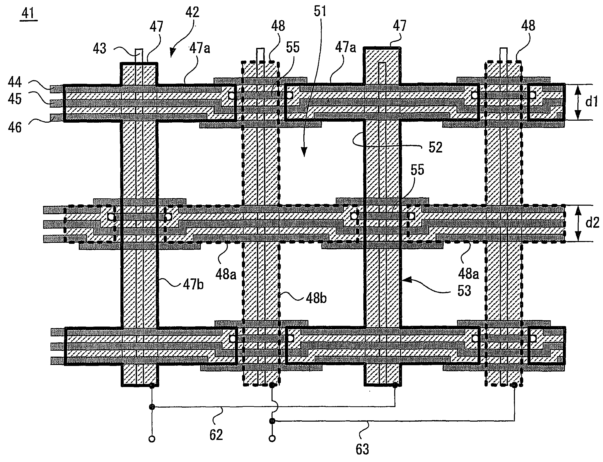
另外,根据本发明实施例的固态成像装置的特征是多个配线中采用的配线结构。图4是根据本发明实施例的固态成像装置的示意图,特别详细地图解了配线结构的第一实例。第一实例的固态成像装置41提供有成像部分42以及转移信号配线44、复位信号配线45和选择信号配线46,成像部分42包括由在第一层上在垂直方向上延伸的金属配线形成的像素输出配线43;而转移信号配线44、复位信号配线45和选择信号配线46的每一个都由在第二层上在水平方向上彼此平行地延伸的金属配线形成。还是在该实例中,电源配线47和接地配线48的每一个都由在第三层上的金属配线形成为彼此部分间断的格子形状。In addition, a solid-state imaging device according to an embodiment of the present invention is characterized by a wiring structure employed in a plurality of wirings. 4 is a schematic diagram of a solid-state imaging device according to an embodiment of the present invention, illustrating a first example of a wiring structure in particular in detail. The solid-
电源配线47形成格子形状作为第一格子结构,其每一个水平梁部分(crosspiece portion)47a在中间分开,而接地配线48类似地形成格子形状作为第二格子结构,其每一个水平梁部分48a在中间分开。这些电源配线47和接地配线48布置为形成组合,从而第二格子结构的垂直梁部分48b和第一格子结构的垂直梁部分47b相互设置为在空间上分别容纳在电源配线47和接地配线48的上述分开的部分中。利用这些电源配线47和接地配线48,遮光部分53形成为格子形状,其提供开口52,每个开口52都形成在空间上对应于包括在像素中的光电转换元件51的位置。The
另外,第一和第二对水平梁47a和48a预先分别与电源配线47和接地配线48分开,在电源配线47和接地配线48的方向彼此交叉的交叉位置上采用连接配线55互连成对,连接配线55用在第二层上的金属配线形成。In addition, the first and second pairs of
转移信号配线44、复位信号配线45和选择信号配线46由在第二层上水平延伸的金属配线形成,彼此平行地分别设置在电源配线47和接地配线48形成为格子结构的水平梁部分47a和48a的线宽d1和d2(在本实例中,d1=d2)之内。然而,因为连接线55形成在电源配线47和接地配线48的上述交叉位置,所以提供在两个外侧上的配线部分——即本实例中转移信号配线44和选择信号配线46的部分——形成为在交叉位置附近从上述线宽部分地突出到开口52的区域中。The
根据本发明实施例的固态成像装置41的配线结构的第一实例,电源配线47和接地配线48的每一个都用在第三层上的金属配线形成为彼此部分间断的格子形状,并且位于电源配线47和接地配线48的交叉位置的间断部分使用在第二层上的金属配线形成的连接配线55互连。另外,利用电源配线47和接地配线48的组合,遮光部分53形成为格子形状。利用固态成像装置的这样的构造,在有效实施像素之间的遮光后,可以改善图像质量,由此控制像素之间的混色。另外,因为扩展了面向光电转换元件51的开口52的面积,所以可以改善聚焦效率,并且总体上增加灵敏度。According to the first example of the wiring structure of the solid-
就是说,在图3所示的情况下,因为第二层上的接地配线33和转移信号配线11形成为突出到由第三层上的格子形状的电源配线10限定的开口10A的区域中,所以开口的有效面积实际限定为电源配线10、转移信号配线11和接地配线33所围绕的面积。在本实例中,相比之下,以还用于遮光的配线形成的开口52的有效面积由第三层上的电源配线47和接地配线48以及第二层上的部分突出的配线(例如转移信号配线44和选择信号配线46)所围绕的区域限定。因此,本实例中的开口的面积可以增加的量为第二层上配线的突出部分的面积的减少的量,并且与图3的先前已知的实例相比,可以改善聚焦效率,以及提高灵敏度。That is, in the case shown in FIG. 3, since the
因为接地配线48形成在第三层上,所以在第二层上的信号配线与接地配线48之间耦合电容减少了。另外,因为接地配线48形成为格子形状,所以其配线寄生电阻变小。尽管连接配线55形成在第二层上,但是配线55与其相邻的信号配线之间的耦合电容可以因线长相对短而保持为小的。对于本配线构造,因为抑制了接地电位的波动,所以可以稳定接地电位。作为稳定接地电位的结果,所以可以抑制噪声的发生。Since the
此外,通过将电源配线47和接地配线48的每一个都形成为格子形状,配线自身的寄生电阻、电容可以保持得小,可以抑制阴影的发生,并因此可以抑制阴影所导致的图像质量的下降。另外,因为与在先已知的结构相比减小了第二层上的配线密度,所以可以实现配线的低电阻和低电容。同样,减少了信号延迟的影响,并且可以抑制由信号延迟引起的图像质量的下降。In addition, by forming each of the
因为配线层数保持为三层,与图3的实例相同,所以可以利用光电转换元件与芯片上透镜之间相对小的距离来实现装置厚度的减小,并且可以改善装置的灵敏度。对于这样的构造,减少了第二层上的配线数,并且因考虑到渐晕的减少可以提高设计配线方案上的灵活性。Since the number of wiring layers is kept at three layers, the same as the example of FIG. 3 , a reduction in device thickness can be achieved with a relatively small distance between the photoelectric conversion element and the on-chip lens, and the sensitivity of the device can be improved. With such a configuration, the number of wires on the second layer is reduced, and the flexibility in designing the wiring scheme can be improved by considering the reduction of vignetting.
在第一实例中,如上所述,格子形状的电源配线47和接地配线48的每一个都用在第三层上的金属配线形成,并且遮光部分53利用电源配线47和接地配线48的组合形成为另一格子形状。另外,遮光部分53也可以这样来提供,首先,使用信号配线44、45和46中的任何一个以及电源配线47和接地配线48中的一个在第三层上形成金属配线的格子结构,并与图4类似的方式彼此部分分开;然后,使用连接配线55将这两个格子结构组合起来。在此情况下,电源配线47和接地配线48的另一个与彼此平行地水平延伸的其它信号配线一起形成为第二层上的另一个金属配线。In the first example, as described above, each of the grid-shaped
关于本装置的构造,可以增加遮光部分中开口的面积,并且取得灵敏度的改善。另外,由于减少了电阻和电容,还可以实现图像质量的改善。Regarding the configuration of the present device, it is possible to increase the area of the opening in the light-shielding portion, and to achieve improvement in sensitivity. In addition, an improvement in image quality can also be achieved due to the reduction of resistance and capacitance.
图5是根据本发明实施例的固态成像装置的示意图,部分地详细图解了配线结构的第二实例。第二实例的固态成像装置61提供有成像部分42以及转移信号配线44、复位信号配线45和选择信号配线46,成像部分42包括由在第一层上在垂直方向上延伸的金属配线形成的像素输出配线43,转移信号配线44、复位信号配线45和选择信号配线46的每一个都由在第二层上在水平方向上彼此平行地延伸的金属配线形成。同样在本实例中,电源配线47和接地配线48的每一个都用在第三层上的金属配线形成为彼此部分间断的格子形状。5 is a schematic diagram of a solid-state imaging device according to an embodiment of the present invention, partially illustrating a second example of a wiring structure in detail. The solid-state imaging device 61 of the second example is provided with an
电源配线47形成格子形状作为第一格子结构,其水平梁部分47a的每一个都在中间分开,并且接地配线48类似地形成格子形状作为第二格子结构,其水平梁部分48a的每一个都在中间分开。这些电源配线47和接地配线48布置为形成组合,从而第二格子结构的垂直梁部分48b和第一格子结构的垂直梁部分47b相互设置在空间上分别容纳在电源配线47和接地配线48的上述分开的部分中。通过电源配线47和接地配线48,遮光部分53形成为格子形状,该格子形状提供有开口52,每一个开口52都形成在与像素的光电转换元件51空间上对应的部分。The
另外,电源配线47和接地配线48分别形成为彼此部分间断的格子形状,没有像前述的第一实例那样以采用连接配线的形式连接,而是在它们现在的形状中彼此部分间断的电源配线47采用配线62在配线47的端部互连,同样,在它们现在的形状中彼此部分间断的接地配线48采用配线63在配线48的端部互连。In addition, the
第二层上的转移信号配线44、复位信号配线45和选择信号配线46由线性水平延伸的金属配线形成在整个装置的长度上。两侧的配线例如转移信号配线44和选择信号配线46提供为不突出到开口52的区域中,开口52形成在作为电源配线47和接地配线48的组合的格子形状的遮光部分53中。因为该装置的其它特征类似于上述第一实例的情况,所以在此省略了重复性的描述。The
根据本发明的实施例的固态成像装置61的配线结构的第二实例,格子形状的遮光部分53以在第三层上的金属配线形成为电源配线47和接地配线48的组合的图案,并且第二层上的信号配线44和46形成为不突出到开口52的区域中。因此,开口52面对各光电转换元件的面积得以增加。本实施例中总体上的开口面积可以大于第一实例。所以,可以改善聚焦效率,并且提高灵敏度。According to the second example of the wiring structure of the solid-state imaging device 61 of the embodiment of the present invention, the lattice-shaped
因为接地配线48形成在第三层上,所以第二层上的信号配线与接地配线48之间的耦合电容减少,并且因为接地配线48形成为格子形状,尽管彼此部分间断,然而配线的寄生电阻减少。因此,抑制了接地电位的波动,并且可以稳定接地电位。作为稳定接地电位的结果,可以抑制噪声的发生。Since the
此外,通过将电源配线47和接地配线48的每一个都形成为格子形状,配线自身的寄生电阻、电容可以保持为小的,可以抑制阴影的发生,并且可以抑制因阴影引起的图像质量的下降。另外,因为第二层上的配线密度相对于在先已知的结构减小,所以可以实现配线的低电阻以及低电容。同样,减少了信号延迟的影响,并且可以抑制因信号延迟引起的图像质量的下降。In addition, by forming each of the
因为配线的层数保持为三层,与图3的实例相同,所以可以利用光电转换元件的接收表面与芯片上透镜之间的相对小的距离来实现装置厚度的减少,并且可以改善灵敏度。对于这样的构造,第二层上的配线数可以减少,并且考虑到渐晕的减少可以在设计配线方案上提高灵活性。Since the number of layers of wiring is kept at three layers, the same as the example of FIG. 3 , reduction in device thickness can be achieved with a relatively small distance between the receiving surface of the photoelectric conversion element and the on-chip lens, and sensitivity can be improved. With such a configuration, the number of wires on the second layer can be reduced, and flexibility in designing a wire scheme can be improved in consideration of the reduction of vignetting.
因为在第二实例中电源配线47和接地配线48彼此分开的部分没有采用连接配线互连,所以第一实例的构造对于减少电源配线47和接地配线48的寄生电阻更加有利。第一实例的构造总体上比第二实例更加有利。The configuration of the first example is more advantageous for reducing the parasitic resistance of the
图6是根据本发明实施例的固态成像装置的示意图,特别地详细图解了配线结构的第三实例。第三实例的固态成像装置71提供有成像部分42,成像部分42包括由在第一层上垂直地延伸的金属配线形成的像素输出配线43;和配线中的任意两种(在本实例中为转移信号配线44和复位信号配线45)以及接地配线48用在第二层上水平延伸的金属配线形成。此外,在本实例中,电源配线47和选择信号配线46用在第三层上的金属配线形成,并且格子形状的遮光部分53形成为电源配线47和选择信号配线46的组合。6 is a schematic diagram of a solid-state imaging device according to an embodiment of the present invention, particularly illustrating a third example of a wiring structure in detail. The solid-state imaging device 71 of the third example is provided with an
电源配线47形成为具有相对大的线宽d3,它们之间具有预定的间隔并彼此平行地垂直延伸,它们之间的预定间隔足以使光电转换元件提供在开口部分中。选择信号配线46形成为水平延伸,具有另一个大的线宽d4(在本实例中d3=d4)。选择信号配线46形成为在与电源配线47的交叉位置彼此部分间断,并且其端部在该位置通过第二层上的金属所形成的连接配线72互连。用垂直延伸的电源配线47和水平延伸的选择信号配线46,形成格子形状的遮光部分53,这样在与包括在像素中的光电转换元件51空间上对应的位置提供开口52。电源配线47在配线47的端部使用配线73互连。The
转移信号配线44、复位信号配线45和接地配线48由在第二层上水平延伸的金属配线形成,彼此平行地提供在选择信号配线46的线宽d4内。然而,因为连接配线72形成在电源配线47和选择信号配线46的交叉位置,所以提供在两个外侧上的配线部分,也就是本实例中的接地配线48和转移信号配线44的部分,形成为在交叉位置的附近部分突出到开口52的区域上。因为其它装置特征与第一实例的类似,在此省略其重复性的描述。The
根据本发明实施例的固态成像装置71的配线结构的第三实例,格子形状的遮光部分53使用分别由在第三层上的金属配线形成的垂直延伸的电源配线47和水平延伸的选择信号配线46形成,在对应于包括在像素中的光电转换元件5 1空间上的位置具有开口52。类似于第一实例的情况,提供在遮光部分53中的开口52的面积与在先已知的图3的装置结构中的情况相比较大,开口面积增加了,相应地改善了聚焦效率并提高了灵敏度。According to the third example of the wiring structure of the solid-state imaging device 71 of the embodiment of the present invention, the grid-shaped
另外,通过减少第二层上的配线密度,可以减少接地配线48和复位信号配线45之间的耦合电容,并且也可以减少接地配线48与第三层上的选择信号配线46之间的耦合电容。结果,抑制了接地电位的波动,并且可以稳定接地电位。In addition, by reducing the wiring density on the second layer, the coupling capacitance between the
此外,还是在本实例中,抑制了阴影的发生,并且还可以抑制由阴影引起的图像质量的下降。另外,因为第二层上的配线密度与在先已知的结构相比减小,所以可以实现配线的低电阻和低电容,减少了信号延迟的影响,并且可以抑制由信号延迟引起的图像质量的下降。Furthermore, also in this example, the occurrence of shading is suppressed, and it is also possible to suppress degradation of image quality caused by shading. In addition, since the wiring density on the second layer is reduced compared with the previously known structure, low resistance and low capacitance of the wiring can be realized, the influence of signal delay is reduced, and the effect caused by signal delay can be suppressed. Image quality degradation.
因为配线的层数保持为三层,与图3的实例相同,所以可以利用光电转换元件的接收表面与芯片上透镜之间的相对小的距离来实现装置厚度的减少,并且可以改善灵敏度。关于这样的构造,可以减少第二层上的配线数,并且由于考虑到渐晕的减少可以增加设计配线方案上的灵活性。Since the number of layers of wiring is kept at three layers, the same as the example of FIG. 3 , reduction in device thickness can be achieved with a relatively small distance between the receiving surface of the photoelectric conversion element and the on-chip lens, and sensitivity can be improved. With such a configuration, the number of wirings on the second layer can be reduced, and flexibility in designing a wiring scheme can be increased due to consideration of reduction in vignetting.
第一和第二实例的构造总体上比第三实例更加有利。The configurations of the first and second examples are generally more favorable than the third example.
在根据本实施例的第三实例中,配线结构还可以这样来提供,通过用转移信号配线44或者复位信号配线45来代替选择信号配线46。另外,使用第三层上的格子形状的金属配线来形成选自包括像素输出配线43和驱动配线44、45和46的组中的两种配线也是可行的。再者,配线的层数不限于三层,而是还可以为两层、四层或者更多层。In the third example according to the present embodiment, the wiring structure can also be provided by replacing the
在上面的实例中,采用包括转移、复位、放大和选择晶体管的四晶体管电路构造描述了用于形成单元像素的像素晶体管。根据本发明的实施例,可以采用包括除选择晶体管外的转移、复位和放大晶体管的三晶体管电路构造。此外,本发明的实施例也可以应用于所谓的像素共享型CMOS图像传感器,其中多个组共享像素晶体管,每个组形成为包括一个光电转换元件和一个转移晶体管。In the above examples, a pixel transistor for forming a unit pixel was described using a four-transistor circuit configuration including transfer, reset, amplification, and selection transistors. According to an embodiment of the present invention, a three-transistor circuit configuration including transfer, reset, and amplifying transistors in addition to a selection transistor may be employed. Furthermore, the embodiment of the present invention can also be applied to a so-called pixel sharing type CMOS image sensor in which pixel transistors are shared by a plurality of groups each formed to include one photoelectric conversion element and one transfer transistor.
接下来,在根据上述实施例的固态成像装置中,描述几种构造,用于从外部提供电源或者电源及信号二者到第三层上的不同配线。Next, in the solid-state imaging devices according to the above-described embodiments, several configurations are described for externally supplying power or both power and signals to different wirings on the third layer.
在描述上述供给构造之前,首先将描述一个实例,该构造与在先已知的情况相比适合于给一个层上的不同配线提供不同的电压,例如电源或者电源及接地二者。该示范性构造可以使用在本发明的实施例中。Before describing the above supply configuration, an example will first be described which is suitable for supplying different wirings on one layer with different voltages, such as power or both power and ground, than previously known. This exemplary configuration can be used in the embodiments of the present invention.
为了适当确定固态成像装置中的信号的亮度水平(luminance level),有必要设定用作标准的黑度值(black level)。为了确定黑度值,采用光学黑像素(在下文称为OPB像素,OPB-optical black pixel),其通过金属配线遮蔽用作光电转换元件的光敏二极管(PD)形成。考虑到每一个都具体地用在水平或者垂直方向上的配线层的各种不同目的,对于形成遮光金属配线,利用具有空间上对应于每个像素的开口的格子形状的电源配线层是合适的。如图7所示,在OPB像素区域89中的OPB像素82覆盖有遮光金属81,OPB像素82提供在紧邻有效像素85的外侧,以对有效像素区域80中邻近遮光金属81的开口84形成的有效像素85的特性进行适当参考。另外,OPB像素82形成在左、右、上、下四侧上,以消除有效像素区域80中左、右、上、下的有效像素85的特性差别。In order to properly determine the luminance level of a signal in a solid-state imaging device, it is necessary to set a black level used as a standard. To determine the blackness value, an optical black pixel (hereinafter referred to as an OPB pixel, OPB-optical black pixel) formed by shielding a photodiode (PD) serving as a photoelectric conversion element with a metal wiring is used. Considering various purposes of each of the wiring layers specifically used in the horizontal or vertical direction, for forming the light-shielding metal wiring, a grid-shaped power wiring layer having an opening spatially corresponding to each pixel is used. is suitable. As shown in FIG. 7, the
考虑到确定黑度值标准,优选OPB像素82和有效像素85在特性上相同。然而,由于形成在装置上的配线图案上的差别,会引起由电学行为(electrical behavior)和/或制造工艺上的差别造成的特性上的某些偏差。在此情况下,特性上的差别可以通过给OPB像素82和有效像素85提供不同的电源来补偿。如图7所示,当OPB像素区域89中的遮光金属由有效像素区域80中的电源配线层共享时,以及当使用一个单一电源时,电源可以按原样提取到外部。然而,当不同的电源分别提供给有效像素85和OPB像素82时,必须分开引导到各像素的配线,并且将电源分别引导到外部。In consideration of determining the blackness value standard, it is preferable that the
因为有效像素85由OPB像素82围绕,如图8所示,所以在有效像素85所用电源引导到外部的情况下,所预期的结构为使得位于围绕有效像素的OPB像素区域89中的OPB像素82和遮光金属87的某些部分去除,并且到有效像素区域80中的有效像素85的电源配线86可以通过这样的去除部分引导到外部。形成在OPB像素区域89上的遮光金属87用作到OPB像素82的电源配线。Since the
然而,当这样的结构形成有电源配线86和87时,到有效像素85的电源变得不对称。结果,导致显示屏幕的阴影,并且相应于上述OPB像素82的去除,会引起缺少关于左、右、上、下部特性差别的某些信息的可能性。However, when such a structure is formed with the
关于引导不同的电源到外部,在使用第三层上的金属配线形成电源配线47和接地配线48的情况下,产生如本发明的上述实施例中所描述的同样的困难。With regard to leading different power sources to the outside, in the case where the
因此,如图9所示,根据本发明的实施例,当有效像素85中使用的电源从外部提供时,提供遮光金属87之外的另一种结构,从而配线层88的每一个都形成在OPB像素82的上面。关于这样的结构,用于将有效像素区域80中的电源配线86引导到外部的配线层88可以对称地实施在左、右、上、下部。就是说,可以分别给OPB像素82和有效像素区域85提供不同的电源,而不去除OPB像素82的部分,并且不引起任何电源上的不对称。然而,在固态成像装置因其像素尺寸小而难于在像素自身上额外地提供一种配线并且难于采用图9所示装置的情况下,电源还可以实施为图8所示的结构,以使配线不通过光敏二极管的上面。Therefore, as shown in FIG. 9, according to an embodiment of the present invention, when the power used in the
图10的示意图图解了根据本发明实施例的第四实例,其中图9所示用于将电源配线和接地配线引导到外部的构造适合于前述第一实例用于使用在第三层上的金属配线形成电源配线47和接地配线48的构造。根据本实例的固态成像装置75提供为在有效像素区域77中包括电源配线47,在有效像素区域77中设置有有效像素76,每个有效像素76都包括光电转换元件51,在该固态成像装置75中电源配线47形成为延伸到其中设置有周边OPB像素78的OPB像素区域79上,从而作为遮光金属91共享。10 is a schematic diagram illustrating a fourth example according to an embodiment of the present invention, in which the configuration shown in FIG. 9 for leading power wiring and ground wiring to the outside is adapted to the aforementioned first example for use on the third layer The metal wires form the structure of the
在有效像素区域77中,非有效像素区域92形成为邻近OPB像素区域79。In the
另外,根据本实例,有效像素区域77中的接地配线48提供为通过在第三层以外的层上的金属配线引导到外部,在本实例中为第二层上的金属配线的电压供给配线93。同样,在本实例中,电压供给配线93用作提供接地电压的配线。在此情况下,电压供给配线93形成为通过提供在非有效像素区域92和OPB像素78中光电转换元件51的正上方。而且,如图9所示,电压供给配线93形成为上、下以及左、右四侧对称,并且通过形成在周边非有效像素区域92中的每个开口52的上面。用这样的结构,电源电压从周边OPB像素区域79中的遮光金属91提供,而接地电压从电压供给配线93提供。In addition, according to the present example, the
电源配线47和接地配线48的配线图案还可以形成为使它们的作用与图10中的相反,其中接地配线48形成为延伸到OPB像素区域79上,从而也共享为OPB像素区域上的遮光金属,并且电源配线47提供为通过电压供给配线93引导到外部。The wiring patterns of the
在根据本发明实施例的固态成像装置75的配线结构的第四实例中,利用在第三层上形成为上、下、左、右对称的电源配线47和接地配线48,可以提供不同的电源和接地电压。通过在OPB像素区域79中的光电转换元件的正上方形成电压供给配线用于引导接地配线48到外部,可以分别给OPB像素区域79和有效像素区域77提供不同的电压,而不引起电源和接地电压供给上的任何不对称,即使对于每个都具有很小的单元尺寸的像素。In the fourth example of the wiring structure of the solid-
图11的示意图图解了根据本发明实施例的配线结构的第五实例,其中图8所示的将电源配线和接地配线引导到外部的构造用于前述第一实例用于使用第三层上的金属配线形成电源配线47和接地配线48的构造。根据本实例的固态成像装置95提供为去除OPB像素区域79的一部分,并且将电源配线47或者接地配线48(在该实例中为电源配线47)延伸到该去除的部分,以作为遮光金属91共享。另一个配线,即接地配线48,延伸到OPB像素区域79除了去除的部分外的部分,以共享为遮光金属90。OPB像素78的去除的部分可以仅形成在如图8所示的一侧上,并且电源配线47可以仅延伸在一侧上。作为选择,OPB像素78的去除的部分可以提供在两侧上以左右对称,并且电源配线47形成为对称地延伸到该两侧。FIG. 11 is a schematic diagram illustrating a fifth example of a wiring structure according to an embodiment of the present invention, in which the configuration of leading power wiring and ground wiring to the outside shown in FIG. 8 is used for the aforementioned first example for using the third example. The metal wiring on the layer forms the structure of the
就根据本发明实施例的固态成像装置95的配线结构的第五实例而言,可以引导电源配线47和接地配线48到外部,其特别适合于实施在小像素尺寸的固态成像装置中。As for the fifth example of the wiring structure of the solid-
图12的示意图图解了根据本发明实施例的构造的另一个实例,其适合于分别为有效像素区域77和OPB像素区域79提供的不同电源以引导到外部的情况。在除了非有效像素区域92的有效像素区域77中,格子形状的有效像素电源配线96形成来用于遮光,而OPB像素的电源配线97形成在OPB像素区域79中以便也用作遮光金属。这些有效像素电源配线96和OPB像素电源配线97使用在第三层上的金属配线形成。FIG. 12 is a schematic diagram illustrating another example of a configuration according to an embodiment of the present invention, which is suitable for the case where different power supplies are respectively provided to the
另外,有效像素的电源配线96构造为通过在非有效像素区域92和OPB像素78中设置的光电转换元件的上面,并且通过另一层上的电压供给配线93(在本实例中为第二层上的金属配线)引导到外部。利用本结构,可以分别给有效像素的电源配线96和OPB像素的电源配线97提供不同的电压,并且有效像素76和OPB像素78的特性可以彼此进行适当参考。In addition, the
为了比较的目的,图13图解了在先已知的将电源配线引导到外部的实例,对应于图7的情况。为了易于理解,包括在图13中类似于图10、11和12的部分用相同的附图标记表示。参考图13,也用作有效像素区域77的遮光金属的电源配线47形成为延伸到OPB像素区域79。尽管电源配线47也用作OPB像素区域79中的遮光金属,但是由有效像素76和OPB像素78的电源供给所共享。For comparison purposes, FIG. 13 illustrates a previously known example of leading power supply wiring to the outside, corresponding to the case of FIG. 7 . For ease of understanding, portions included in FIG. 13 that are similar to those in FIGS. 10, 11 and 12 are denoted by the same reference numerals. Referring to FIG. 13 , the
接下来,将在下面描述通过第三层上的金属配线分别以不同的电压或者电压和信号提供给两条配线的结构的几个实例。关于引导电源配线到外部,当OPB像素区域中的遮光金属都形成有相同的配线时,上述的供给通常可以从OPB像素区域直接进行(参考图7)。另一方面,当电源优选分成两个时,例如一个用于有效像素区域而另一个用于OPB像素区域,或者一个用于电源配线而另一个用于使用相同层上的金属配线的接地配线,则要么去除OPB像素区域79的一部分,要么给将电压提供给不对称的配线结构(参考图8)。另外,尽管也可以考虑通过遮光金属层之外的层穿过OPB像素区域,但是对于单元尺寸很小的像素难于实施该方法,因为另一个配线必须添加到有效区域。然而,当采用图9所示的构造时,即使在分开电源或者在相同的层上提供电源和接地的情况下,也可以按着要求提供电源电压,这是因为从有效像素区域输出的配线直接形成在OPB像素区域中设置的光电转换元件的上面。例如,即使在小单元尺寸的固态成像装置中,不同的电压也可以分别提供给都在相同层上的OPB像素区域和有效像素区域中的配线,而不去除OPB像素的部分,并且也不引起电压供给上的不对称。Next, several examples of structures in which different voltages or voltages and signals are respectively supplied to two wirings through metal wirings on the third layer will be described below. As for leading the power wiring to the outside, when the light-shielding metals in the OPB pixel area are all formed with the same wiring, the above-mentioned supply can usually be directly performed from the OPB pixel area (refer to FIG. 7 ). On the other hand, when the power supply is preferably divided into two, such as one for the effective pixel area and the other for the OPB pixel area, or one for power supply wiring and the other for ground using metal wiring on the same layer Wiring, either remove a part of the
图9所示的结构适合于前述根据本发明实施例的固态成像装置的配线结构的第一、第二和第三实例。图8的结构也适合于第一、第二和第三实例的固态成像装置。The structure shown in FIG. 9 is suitable for the aforementioned first, second, and third examples of the wiring structure of the solid-state imaging device according to the embodiment of the present invention. The structure of FIG. 8 is also suitable for the solid-state imaging devices of the first, second and third examples.
尽管就关于将电源、接地等连接到有效像素区域已经对引导供给配线到外部的方法进行了说明,但是本方法也可以适用于驱动电路配线等,用于期望地从OPB像素区域的外部通过OPB像素区域输入到有效像素区域。Although the method of guiding supply wiring to the outside has been described with regard to connecting power supply, ground, etc. to the effective pixel area, this method can also be applied to driver circuit wiring, etc. Input to the effective pixel area through the OPB pixel area.
图14的示意图图解了提供有上述根据本发明实施例的固态成像装置的照相机。参考图14,根据本实施例的照相机100提供为包括光学系统(光学透镜)101、固态成像装置102和信号处理电路103。关于固态成像装置102,可以优选采用上述实施例中描述的装置的任何一个,以及提供有配线结构的第一实例或者第四实例的装置。光学系统101构造为用从物体发出的图像光(入射光)在固态成像装置102的成像表面上实施图像形成。包括在固态成像装置102中的光电转换元件将信号电荷积累固定的时间段。信号处理电路103构造为提供给从固态成像装置102输出的信号各种信号处理,并且输出为图片信号。根据本实施例的照相机100还可以包括照相机模块,其通过模块化的光学系统101、固态成像装置102和信号处理电路103形成。FIG. 14 is a schematic diagram illustrating a camera provided with the above-described solid-state imaging device according to an embodiment of the present invention. Referring to FIG. 14 , a
关于根据本实施例的照相机100,因为该照相机结合了根据本发明实施例的固态成像装置,所以可以提供高灵敏度和高质量的图片图像。Regarding the
根据本发明的实施例,可以提供结合前述的图14所示的照相机或者照相机模块的诸如移动电话为代表的移动装置的各种电子装置。关于根据本发明实施例的电子装置,因为包括能够提供高灵敏度和高质量的图片图像的照相机,所以可以提供高性能的电子装置。According to an embodiment of the present invention, various electronic devices such as a mobile device typified by a mobile phone incorporating the aforementioned camera or camera module shown in FIG. 14 can be provided. Regarding the electronic device according to the embodiment of the present invention, since a camera capable of providing a high-sensitivity and high-quality picture image is included, a high-performance electronic device can be provided.
本领域的技术人员应当理解的是,在权利要求或其等同特征的范围内,根据设计需要和其它因素,可以进行各种修改、结合、部分结合和替换。It should be understood by those skilled in the art that various modifications, combinations, partial combinations and substitutions may be made according to design requirements and other factors within the scope of the claims or their equivalents.
本发明包含2008年2月15日提交至日本专利局的日本专利申请JP2008-035361相关的主题,将其全部内容引用结合于此。The present invention contains subject matter related to Japanese Patent Application JP2008-035361 filed in the Japan Patent Office on Feb. 15, 2008, the entire content of which is hereby incorporated by reference.
Claims (19)
Applications Claiming Priority (2)
| Application Number | Priority Date | Filing Date | Title |
|---|---|---|---|
| JP035361/08 | 2008-02-15 | ||
| JP2008035361A JP5130946B2 (en) | 2008-02-15 | 2008-02-15 | Solid-state imaging device, camera and electronic device |
Publications (2)
| Publication Number | Publication Date |
|---|---|
| CN101510552A CN101510552A (en) | 2009-08-19 |
| CN101510552B true CN101510552B (en) | 2011-05-11 |
Family
ID=40954768
Family Applications (1)
| Application Number | Title | Priority Date | Filing Date |
|---|---|---|---|
| CN2009100063616A Expired - Fee Related CN101510552B (en) | 2008-02-15 | 2009-02-16 | Solid-state imaging device, camera, and electronic device |
Country Status (5)
| Country | Link |
|---|---|
| US (2) | US8134625B2 (en) |
| JP (1) | JP5130946B2 (en) |
| KR (1) | KR20090088790A (en) |
| CN (1) | CN101510552B (en) |
| TW (1) | TWI412271B (en) |
Families Citing this family (23)
| Publication number | Priority date | Publication date | Assignee | Title |
|---|---|---|---|---|
| JP5130946B2 (en) * | 2008-02-15 | 2013-01-30 | ソニー株式会社 | Solid-state imaging device, camera and electronic device |
| JP5564874B2 (en) | 2009-09-25 | 2014-08-06 | ソニー株式会社 | Solid-state imaging device and electronic apparatus |
| JP5422455B2 (en) * | 2010-03-23 | 2014-02-19 | パナソニック株式会社 | Solid-state imaging device |
| US9473714B2 (en) * | 2010-07-01 | 2016-10-18 | Semiconductor Energy Laboratory Co., Ltd. | Solid-state imaging device and semiconductor display device |
| JP2012049431A (en) * | 2010-08-30 | 2012-03-08 | Sony Corp | Solid state imaging device and electronic apparatus |
| US9252171B2 (en) | 2010-09-06 | 2016-02-02 | Semiconductor Energy Laboratory Co., Ltd. | Electronic device |
| JP5967915B2 (en) * | 2011-12-09 | 2016-08-10 | キヤノン株式会社 | Driving method of solid-state imaging device |
| JP5907176B2 (en) * | 2011-12-28 | 2016-04-26 | 株式会社ニコン | Imaging device |
| JP2013149758A (en) * | 2012-01-18 | 2013-08-01 | Canon Inc | Solid state image pickup device and method of manufacturing the same, and camera |
| US8779592B2 (en) * | 2012-05-01 | 2014-07-15 | Taiwan Semiconductor Manufacturing Company, Ltd. | Via-free interconnect structure with self-aligned metal line interconnections |
| JP2015037158A (en) * | 2013-08-15 | 2015-02-23 | ソニー株式会社 | Solid-state imaging element, electronic apparatus, and inspection device |
| JP6148580B2 (en) * | 2013-09-03 | 2017-06-14 | キヤノン株式会社 | Imaging apparatus and camera |
| JP2015079899A (en) * | 2013-10-18 | 2015-04-23 | ソニー株式会社 | Solid-state imaging device and electronic device |
| KR20220100106A (en) | 2014-06-09 | 2022-07-14 | 가부시키가이샤 한도오따이 에네루기 켄큐쇼 | Imaging device |
| TWI700823B (en) * | 2014-06-27 | 2020-08-01 | 日商半導體能源研究所股份有限公司 | Imaging device and electronic device |
| JP6587497B2 (en) * | 2014-10-31 | 2019-10-09 | 株式会社半導体エネルギー研究所 | Semiconductor device |
| US9729242B2 (en) * | 2015-01-23 | 2017-08-08 | Furukawa Electric Co., Ltd. | Optical module for reducing crosstalk |
| CN108702471B (en) * | 2016-02-29 | 2021-10-22 | 索尼公司 | Solid State Camera |
| JP6910814B2 (en) * | 2017-02-22 | 2021-07-28 | ソニーセミコンダクタソリューションズ株式会社 | Solid-state image sensor and electronic equipment |
| JP2021176154A (en) * | 2018-07-18 | 2021-11-04 | ソニーセミコンダクタソリューションズ株式会社 | Light receiving element and ranging module |
| JP7467061B2 (en) * | 2019-10-09 | 2024-04-15 | 株式会社ジャパンディスプレイ | Detection device |
| CN115836111B (en) * | 2020-07-10 | 2024-07-12 | 东洋纺Mc株式会社 | Inorganic reinforced polyamide resin composition |
| JP2022070502A (en) * | 2020-10-27 | 2022-05-13 | ソニーセミコンダクタソリューションズ株式会社 | Imaging device and electronic apparatus |
Citations (1)
| Publication number | Priority date | Publication date | Assignee | Title |
|---|---|---|---|---|
| CN1212567A (en) * | 1997-08-15 | 1999-03-31 | 索尼株式会社 | Solid state image sensor and method of driving same |
Family Cites Families (15)
| Publication number | Priority date | Publication date | Assignee | Title |
|---|---|---|---|---|
| JPH01276875A (en) * | 1988-04-27 | 1989-11-07 | Mitsubishi Electric Corp | One-dimensional image sensor |
| JPH06283694A (en) * | 1993-03-24 | 1994-10-07 | Sony Corp | Amplification type solid-state image sensor |
| JP2541470B2 (en) * | 1993-08-26 | 1996-10-09 | 日本電気株式会社 | Solid-state imaging device |
| JP3496918B2 (en) * | 1997-12-26 | 2004-02-16 | キヤノン株式会社 | Solid-state imaging device |
| JPH11204768A (en) | 1998-01-09 | 1999-07-30 | Toshiba Corp | Solid-state imaging device and imaging system having the same |
| JP4078707B2 (en) * | 1998-03-19 | 2008-04-23 | 株式会社ニコン | Imaging device |
| JP4164733B2 (en) | 2002-02-05 | 2008-10-15 | ソニー株式会社 | Solid-state imaging device and driving method thereof |
| JP2004104203A (en) | 2002-09-05 | 2004-04-02 | Toshiba Corp | Solid-state imaging device |
| JP4337373B2 (en) * | 2003-03-13 | 2009-09-30 | 株式会社ニコン | Solid-state imaging device and solid-state imaging device using the same |
| JP4403383B2 (en) | 2004-01-27 | 2010-01-27 | ソニー株式会社 | Solid-state imaging device |
| JP4315032B2 (en) | 2004-03-22 | 2009-08-19 | ソニー株式会社 | Solid-state imaging device and driving method of solid-state imaging device |
| JP2007243093A (en) * | 2006-03-13 | 2007-09-20 | Matsushita Electric Ind Co Ltd | Solid-state imaging device, imaging device, and signal processing method |
| KR20070093335A (en) * | 2006-03-13 | 2007-09-18 | 마쯔시다덴기산교 가부시키가이샤 | Solid state imaging device and driving method thereof |
| JP2007243094A (en) * | 2006-03-13 | 2007-09-20 | Matsushita Electric Ind Co Ltd | Solid-state imaging device |
| JP5130946B2 (en) * | 2008-02-15 | 2013-01-30 | ソニー株式会社 | Solid-state imaging device, camera and electronic device |
-
2008
- 2008-02-15 JP JP2008035361A patent/JP5130946B2/en not_active Expired - Fee Related
- 2008-12-15 TW TW097148816A patent/TWI412271B/en not_active IP Right Cessation
- 2008-12-15 US US12/314,674 patent/US8134625B2/en not_active Expired - Fee Related
-
2009
- 2009-01-07 KR KR1020090001049A patent/KR20090088790A/en not_active Ceased
- 2009-02-16 CN CN2009100063616A patent/CN101510552B/en not_active Expired - Fee Related
-
2012
- 2012-03-13 US US13/419,008 patent/US8817152B2/en not_active Expired - Fee Related
Patent Citations (1)
| Publication number | Priority date | Publication date | Assignee | Title |
|---|---|---|---|---|
| CN1212567A (en) * | 1997-08-15 | 1999-03-31 | 索尼株式会社 | Solid state image sensor and method of driving same |
Also Published As
| Publication number | Publication date |
|---|---|
| KR20090088790A (en) | 2009-08-20 |
| US20120224090A1 (en) | 2012-09-06 |
| US20090207291A1 (en) | 2009-08-20 |
| TWI412271B (en) | 2013-10-11 |
| JP2009194260A (en) | 2009-08-27 |
| JP5130946B2 (en) | 2013-01-30 |
| CN101510552A (en) | 2009-08-19 |
| US8134625B2 (en) | 2012-03-13 |
| TW200935888A (en) | 2009-08-16 |
| US8817152B2 (en) | 2014-08-26 |
Similar Documents
| Publication | Publication Date | Title |
|---|---|---|
| CN101510552B (en) | Solid-state imaging device, camera, and electronic device | |
| KR101710021B1 (en) | Image pickup device and image pickup apparatus | |
| JP6334203B2 (en) | Solid-state imaging device and electronic device | |
| JP6126666B2 (en) | Solid-state imaging device and electronic apparatus | |
| KR102060843B1 (en) | Solid-state image pickup element and electronic apparatus | |
| JP7497396B2 (en) | Image pickup element and image pickup device | |
| US9190449B2 (en) | Image pickup apparatus including signal holding units | |
| JP2016019137A (en) | Solid-state imaging device and driving method thereof | |
| JP2010021450A (en) | Solid-state image sensor | |
| JP5619093B2 (en) | Solid-state imaging device and solid-state imaging system | |
| JP2017139498A (en) | Solid-state image pickup device and electronic apparatus |
Legal Events
| Date | Code | Title | Description |
|---|---|---|---|
| C06 | Publication | ||
| PB01 | Publication | ||
| C10 | Entry into substantive examination | ||
| SE01 | Entry into force of request for substantive examination | ||
| C14 | Grant of patent or utility model | ||
| GR01 | Patent grant | ||
| CF01 | Termination of patent right due to non-payment of annual fee |
Granted publication date: 20110511 Termination date: 20150216 |
|
| EXPY | Termination of patent right or utility model |