CN101436606A - Nonvolatile semiconductor memory device - Google Patents
Nonvolatile semiconductor memory device Download PDFInfo
- Publication number
- CN101436606A CN101436606A CNA2008101740296A CN200810174029A CN101436606A CN 101436606 A CN101436606 A CN 101436606A CN A2008101740296 A CNA2008101740296 A CN A2008101740296A CN 200810174029 A CN200810174029 A CN 200810174029A CN 101436606 A CN101436606 A CN 101436606A
- Authority
- CN
- China
- Prior art keywords
- layer
- recording material
- volatile recording
- metal wiring
- mentioned
- Prior art date
- Legal status (The legal status is an assumption and is not a legal conclusion. Google has not performed a legal analysis and makes no representation as to the accuracy of the status listed.)
- Pending
Links
Images


Classifications
-
- H—ELECTRICITY
- H10—SEMICONDUCTOR DEVICES; ELECTRIC SOLID-STATE DEVICES NOT OTHERWISE PROVIDED FOR
- H10N—ELECTRIC SOLID-STATE DEVICES NOT OTHERWISE PROVIDED FOR
- H10N70/00—Solid-state devices without a potential-jump barrier or surface barrier, and specially adapted for rectifying, amplifying, oscillating or switching
- H10N70/20—Multistable switching devices, e.g. memristors
-
- H—ELECTRICITY
- H01—ELECTRIC ELEMENTS
- H01L—SEMICONDUCTOR DEVICES NOT COVERED BY CLASS H10
- H01L27/00—Devices consisting of a plurality of semiconductor or other solid-state components formed in or on a common substrate
- H01L27/02—Devices consisting of a plurality of semiconductor or other solid-state components formed in or on a common substrate including semiconductor components specially adapted for rectifying, oscillating, amplifying or switching and having at least one potential-jump barrier or surface barrier; including integrated passive circuit elements with at least one potential-jump barrier or surface barrier
- H01L27/04—Devices consisting of a plurality of semiconductor or other solid-state components formed in or on a common substrate including semiconductor components specially adapted for rectifying, oscillating, amplifying or switching and having at least one potential-jump barrier or surface barrier; including integrated passive circuit elements with at least one potential-jump barrier or surface barrier the substrate being a semiconductor body
- H01L27/10—Devices consisting of a plurality of semiconductor or other solid-state components formed in or on a common substrate including semiconductor components specially adapted for rectifying, oscillating, amplifying or switching and having at least one potential-jump barrier or surface barrier; including integrated passive circuit elements with at least one potential-jump barrier or surface barrier the substrate being a semiconductor body including a plurality of individual components in a repetitive configuration
- H01L27/101—Devices consisting of a plurality of semiconductor or other solid-state components formed in or on a common substrate including semiconductor components specially adapted for rectifying, oscillating, amplifying or switching and having at least one potential-jump barrier or surface barrier; including integrated passive circuit elements with at least one potential-jump barrier or surface barrier the substrate being a semiconductor body including a plurality of individual components in a repetitive configuration including resistors or capacitors only
-
- G—PHYSICS
- G11—INFORMATION STORAGE
- G11C—STATIC STORES
- G11C5/00—Details of stores covered by group G11C11/00
- G11C5/02—Disposition of storage elements, e.g. in the form of a matrix array
-
- H—ELECTRICITY
- H10—SEMICONDUCTOR DEVICES; ELECTRIC SOLID-STATE DEVICES NOT OTHERWISE PROVIDED FOR
- H10B—ELECTRONIC MEMORY DEVICES
- H10B63/00—Resistance change memory devices, e.g. resistive RAM [ReRAM] devices
-
- H—ELECTRICITY
- H10—SEMICONDUCTOR DEVICES; ELECTRIC SOLID-STATE DEVICES NOT OTHERWISE PROVIDED FOR
- H10B—ELECTRONIC MEMORY DEVICES
- H10B63/00—Resistance change memory devices, e.g. resistive RAM [ReRAM] devices
- H10B63/20—Resistance change memory devices, e.g. resistive RAM [ReRAM] devices comprising selection components having two electrodes, e.g. diodes
-
- H—ELECTRICITY
- H10—SEMICONDUCTOR DEVICES; ELECTRIC SOLID-STATE DEVICES NOT OTHERWISE PROVIDED FOR
- H10B—ELECTRONIC MEMORY DEVICES
- H10B63/00—Resistance change memory devices, e.g. resistive RAM [ReRAM] devices
- H10B63/80—Arrangements comprising multiple bistable or multi-stable switching components of the same type on a plane parallel to the substrate, e.g. cross-point arrays
-
- H—ELECTRICITY
- H10—SEMICONDUCTOR DEVICES; ELECTRIC SOLID-STATE DEVICES NOT OTHERWISE PROVIDED FOR
- H10N—ELECTRIC SOLID-STATE DEVICES NOT OTHERWISE PROVIDED FOR
- H10N70/00—Solid-state devices without a potential-jump barrier or surface barrier, and specially adapted for rectifying, amplifying, oscillating or switching
- H10N70/011—Manufacture or treatment of multistable switching devices
- H10N70/061—Patterning of the switching material
- H10N70/063—Patterning of the switching material by etching of pre-deposited switching material layers, e.g. lithography
-
- H—ELECTRICITY
- H10—SEMICONDUCTOR DEVICES; ELECTRIC SOLID-STATE DEVICES NOT OTHERWISE PROVIDED FOR
- H10N—ELECTRIC SOLID-STATE DEVICES NOT OTHERWISE PROVIDED FOR
- H10N70/00—Solid-state devices without a potential-jump barrier or surface barrier, and specially adapted for rectifying, amplifying, oscillating or switching
- H10N70/20—Multistable switching devices, e.g. memristors
- H10N70/231—Multistable switching devices, e.g. memristors based on solid-state phase change, e.g. between amorphous and crystalline phases, Ovshinsky effect
-
- H—ELECTRICITY
- H10—SEMICONDUCTOR DEVICES; ELECTRIC SOLID-STATE DEVICES NOT OTHERWISE PROVIDED FOR
- H10N—ELECTRIC SOLID-STATE DEVICES NOT OTHERWISE PROVIDED FOR
- H10N70/00—Solid-state devices without a potential-jump barrier or surface barrier, and specially adapted for rectifying, amplifying, oscillating or switching
- H10N70/20—Multistable switching devices, e.g. memristors
- H10N70/24—Multistable switching devices, e.g. memristors based on migration or redistribution of ionic species, e.g. anions, vacancies
- H10N70/245—Multistable switching devices, e.g. memristors based on migration or redistribution of ionic species, e.g. anions, vacancies the species being metal cations, e.g. programmable metallization cells
-
- H—ELECTRICITY
- H10—SEMICONDUCTOR DEVICES; ELECTRIC SOLID-STATE DEVICES NOT OTHERWISE PROVIDED FOR
- H10N—ELECTRIC SOLID-STATE DEVICES NOT OTHERWISE PROVIDED FOR
- H10N70/00—Solid-state devices without a potential-jump barrier or surface barrier, and specially adapted for rectifying, amplifying, oscillating or switching
- H10N70/801—Constructional details of multistable switching devices
- H10N70/821—Device geometry
- H10N70/826—Device geometry adapted for essentially vertical current flow, e.g. sandwich or pillar type devices
-
- H—ELECTRICITY
- H10—SEMICONDUCTOR DEVICES; ELECTRIC SOLID-STATE DEVICES NOT OTHERWISE PROVIDED FOR
- H10N—ELECTRIC SOLID-STATE DEVICES NOT OTHERWISE PROVIDED FOR
- H10N70/00—Solid-state devices without a potential-jump barrier or surface barrier, and specially adapted for rectifying, amplifying, oscillating or switching
- H10N70/801—Constructional details of multistable switching devices
- H10N70/881—Switching materials
- H10N70/882—Compounds of sulfur, selenium or tellurium, e.g. chalcogenides
- H10N70/8825—Selenides, e.g. GeSe
-
- H—ELECTRICITY
- H10—SEMICONDUCTOR DEVICES; ELECTRIC SOLID-STATE DEVICES NOT OTHERWISE PROVIDED FOR
- H10N—ELECTRIC SOLID-STATE DEVICES NOT OTHERWISE PROVIDED FOR
- H10N70/00—Solid-state devices without a potential-jump barrier or surface barrier, and specially adapted for rectifying, amplifying, oscillating or switching
- H10N70/801—Constructional details of multistable switching devices
- H10N70/881—Switching materials
- H10N70/882—Compounds of sulfur, selenium or tellurium, e.g. chalcogenides
- H10N70/8828—Tellurides, e.g. GeSbTe
-
- G—PHYSICS
- G11—INFORMATION STORAGE
- G11C—STATIC STORES
- G11C13/00—Digital stores characterised by the use of storage elements not covered by groups G11C11/00, G11C23/00, or G11C25/00
- G11C13/0002—Digital stores characterised by the use of storage elements not covered by groups G11C11/00, G11C23/00, or G11C25/00 using resistive RAM [RRAM] elements
- G11C13/0004—Digital stores characterised by the use of storage elements not covered by groups G11C11/00, G11C23/00, or G11C25/00 using resistive RAM [RRAM] elements comprising amorphous/crystalline phase transition cells
-
- G—PHYSICS
- G11—INFORMATION STORAGE
- G11C—STATIC STORES
- G11C2213/00—Indexing scheme relating to G11C13/00 for features not covered by this group
- G11C2213/70—Resistive array aspects
- G11C2213/71—Three dimensional array
-
- G—PHYSICS
- G11—INFORMATION STORAGE
- G11C—STATIC STORES
- G11C2213/00—Indexing scheme relating to G11C13/00 for features not covered by this group
- G11C2213/70—Resistive array aspects
- G11C2213/72—Array wherein the access device being a diode
Abstract
The invention provides a nonvolatile semiconductor memory device. In a phase change memory and the like, a problem that atoms of a layer adjointing with a recording material layer are diffused into the recording material layer due to the heat of rewriting operation, when forming a recording material by films and selecting elements of both parties, and the rewriting property changes. In order to solve the problem, the invention provides a semiconductor layer (222) between the nonvolatile recording material layer (224) and the selector element (220, 221), and having a thickness ranging from 5 to 200 nm. Thereby, a nonvolatile memory device having a large storage capacity and stabilized rewriting conditions, can be obtained.
Description
Technical field
The present invention relates to store non-volatilely resistance value that crystalline state and the phase transformation between the non-crystalline state by metallic compound decide, can carry out the phase-changing storage device that electricity rewrites.
Background technology
In nonvolatile semiconductor memory member, the memory device that has is used as stored information with the crystalline state and the non-crystalline state of metallic compound.As this storage medium, use tellurium compound usually.Utilize the difference of their reflectivity to come the principle of stored information to be widely used in optical information storage medium as DVD (digital video disk).
In recent years, proposition is applied to the electrical information storage with this principle.This method is different with optical means, be with the magnitude of current or change in voltage detect amorphous and crystallization resistance difference, be the high resistance state of amorphous and the low resistance state of crystallization.The electrical information memory storing that is applied to the latter is called phase transition storage, and the structure of the basic storage unit of phase transition storage is with the phase change resistor element and selects elements combination structure together.The Joule heat that the phase transition storage utilization produces by the phase change resistor element is applied electric current make the phase change resistor element inscape, be that the non-volatile recording material layer is crystalline state or non-crystalline state.Phase transition storage is stored maintenance information by crystalline state or the non-crystalline state of keeping the non-volatile recording material layer.For rewriting, when being electric high resistance non-crystalline state, make applying big electric current temperature as the resistance variation material of non-volatile memory material be more than the fusing point after, cool off fast and get final product, when being electric low resistance non-crystalline state, the electric current that restriction applies and to make the temperature of resistance variation material be that the crystallization temperature that is lower than fusing point gets final product.Usually the variation about 2 figure places~3 figure places can take place because of phase transformation in the resistance value of non-volatile recording material layer.Therefore, phase transition storage utilizes crystallization or amorphous and the signal read has more differently, is easy to the work of reading.
Patent documentation 1:US 2006/020354/A1
Patent documentation 2:US 6,426,891B1
Summary of the invention
In the rewriting of in the past phase transition storage, change to non-crystalline state mutually or change to crystalline state mutually from crystalline state, so the non-volatile recording material layer is heated to very high temperature from non-crystalline state.Therefore, along with rewriteeing repeatedly, the atom that has the approaching film of formation and non-volatile recording material layer is from the film diffusion approaching with the non-volatile recording material layer, the problem that the rewriting condition changes.
In the technology that prior art, for example US 2006/020354/A1 (patent documentation 1) are put down in writing, be electrically connected the metal film that becomes resistance at the non-volatile recording material layer with selecting to dispose between the element, but metallic element spreads to the non-volatile recording material layer from metal film, the rewriting condition changes, and this becomes a problem.At US 6,426, among the 891B1 (patent documentation 2), between non-volatile recording material layer and selection element, dispose the conductivity thermal isolation film for what prevent from when rewriteeing, to take place from the thermal diffusion of non-volatile recording material layer, but have the decrystallized required such problem of quick cooling that is difficult to carry out the non-volatile recording material layer.The object of the present invention is to provide a kind of phase transition storage, even it prevents from from the layer diffusing atom adjacent with the non-volatile recording material layer or diffusion has taken place also to become the atom that does not influence the rewriting condition, and then also be used for decrystallized quick cooling easily, thereby keep stable rewriting condition.
Exemplify the application's representative art scheme, non-volatile memory semiconductor device of the present invention comprises first electrode, second electrode, is formed on the non-volatile recording material layer between first electrode and second electrode and selects element, is formed on the semiconductor layer that comprises the contained element of non-volatile recording material layer between non-volatile recording material layer and the selection element.Below, will be formed on the non-volatile recording material layer and select the semiconductor layer that comprises the contained element of non-volatile recording material layer between the element to abbreviate semiconductor layer as.
According to the present invention, can obtain rewriteeing the phase transition storage of conditional stability.For example realize to be to carry out 10 below the 50ns in the rewriting time
9The inferior above nonvolatile memory that rewrites.
Description of drawings
Fig. 1 be embodiment of the present invention 1 memory cell want portion's cutaway view.
Fig. 2 be embodiment of the present invention 2 memory cell want portion's cutaway view.
Fig. 3 be embodiment of the present invention 3 memory cell want portion's cutaway view.
Fig. 4 be embodiment of the present invention 4 memory cell want portion's cutaway view.
Fig. 5 represents the overview in the manufacturing process of semiconductor device of embodiment of the present invention 1.
Fig. 6 is the figure of the position relation of expression silicon substrate, peripheral circuit portion and memory matrix portion.
Fig. 7 is the figure of the position relation of expression silicon substrate, peripheral circuit portion and memory matrix portion.
Fig. 8 is the figure of the position relation of expression silicon substrate, peripheral circuit portion and memory matrix portion.
Fig. 9 is the overview in the manufacturing process of the then semiconductor device of Fig. 5.
Figure 10 is the overview in the manufacturing process of the then semiconductor device of Fig. 9.
Figure 11 is the overview in the manufacturing process of the then semiconductor device of Figure 10.
Figure 12 is the overview in the manufacturing process of the then semiconductor device of Figure 11.
Figure 13 is the overview in the manufacturing process of the then semiconductor device of Figure 12.
Figure 14 is the overview in the manufacturing process of the then semiconductor device of Figure 13.
Figure 15 is the overview in the manufacturing process of the then semiconductor device of Figure 14.
Figure 16 is the overview in the manufacturing process of the then semiconductor device of Figure 15.
Figure 17 is the overview in the manufacturing process of the then semiconductor device of Figure 16.
Figure 18 is the overview in the manufacturing process of the then semiconductor device of Figure 17.
Figure 19 is the corresponding vertical view of being put down in writing with Figure 18 of structure.
Figure 20 be expression semiconductor device of the present invention memory matrix want portion's circuit diagram.
Figure 21 represents the overview in the manufacturing process of semiconductor device of embodiment of the present invention 1.
Figure 22 represents the overview in the manufacturing process of semiconductor device of embodiment of the present invention 2.
Figure 23 is the overview in the manufacturing process of the then semiconductor device of Figure 22.
Figure 24 is the overview in the manufacturing process of the then semiconductor device of Figure 23.
Figure 25 is the overview in the manufacturing process of the then semiconductor device of Figure 24.
Figure 26 is the overview in the manufacturing process of the then semiconductor device of Figure 25.
Figure 27 is the overview in the manufacturing process of the then semiconductor device of Figure 26.
Figure 28 is the figure relevant with the optical constant of Si-Ge.
Figure 29 is the overview in the manufacturing process of the then semiconductor device of Figure 27.
Figure 30 is the corresponding vertical view of being put down in writing with Figure 29 of structure.
Figure 31 represents the overview in the manufacturing process of semiconductor device of embodiment of the present invention 4.
Figure 32 represents the overview in the manufacturing process of semiconductor device of embodiment of the present invention 5.
Embodiment
Use Fig. 1~Fig. 4 that the memory cell of nonvolatile memory of the present invention is described.About its structure, with the non-volatile recording material layer and select element be positioned at different layers, through stick harness (plug) and the structure difference that is electrically connected, be without stick harness with one deck with non-volatile recording material layer and the so-called cylindrical configuration of selecting element to be electrically connected.In addition, be that example be illustrated as selecting element with the pn polysilicon diode at this.Therefore, in Fig. 1~Fig. 4,, also can be the structure of other knots as np knot, pin knot though show first polysilicon layer and second polysilicon layer that forms the pn knot.Perhaps, can use the selection element of Schottky (Schottky) knot that has adopted metal wiring layer and polysilicon layer at memory cell.At this with Ge
2Sb
2Te
5Be example explanation non-volatile recording material layer, but by selecting to access the performance of equal extent with the composition that comprises the material of at least a element in the chalcogen (S, Se, Te).
In each following embodiment, to summing up explanation by stacked structure of the lamination order that has nothing in common with each other and suitable thickness.
What Fig. 1 represented is that first polysilicon layer 107, second polysilicon layer 106, semiconductor layer 105, non-volatile recording material layer 104, second metal wiring layer 103, the 3rd metal wiring layer 101 are stacked gradually the embodiment 1 described structure that forms on first metal wiring layer 102.
Non-volatile recording material layer 104 is formed on semiconductor layer 105, first polysilicon layer 107 and second polysilicon layer 106.So, be provided with semiconductor layer 105 between pn polysilicon diode that is made of first polysilicon layer 107 and second polysilicon layer 106 and non-volatile recording material layer 104, the heat atom diffusion as doping impurity in the pn polysilicon diode that produces in the time of therefore can suppressing because of rewriting work arrives non-volatile recording material layer 104.The thickness of semiconductor layer 105 is blocked up still to be to approach all can not bring into play function.If blocked up, though conductivity is then arranged, resistance is excessive, makes the temperature surplus deficiency of the resistance value of non-volatile recording material layer 104 because of its temperature dependency.As if thin excessively, then, the storage of non-volatile recording material layer 104 can not prevent to select the deterioration in characteristics of element because writing the fashionable rising of temperature repeatedly.
Relation about the resistance ratio at high temperature of thickness and low resistance state, high resistance state, when the thickness of semiconductor layer 105 is 160nm, the resistance ratio of low resistance state, high resistance state is about 1:20, when thickness is 200nm, resistance ratio is about 1:10, when thickness was 240nm, resistance ratio was about 1:5.In such resistive nonvolatile memory, consider that from the viewpoint that prevents to misread out the resistance ratio that need make low resistance state and high resistance state is about 10 times, therefore, the thickness of semiconductor layer 105 is below the 200nm.
In addition, but for the relation of thickness and number of rewrites, when the thickness of semiconductor layer 105 is 3nm, but number of rewrites is about 10
5Inferior, when the thickness of semiconductor layer 105 is 5nm, but number of rewrites is about 10
6Inferior, when the thickness of semiconductor layer 105 is 8nm, but number of rewrites is about 10
6Inferior.In the resistive nonvolatile memory, need have about 10 at least
6But inferior number of rewrites, so the thickness of semiconductor layer 105 is more than the 5nm.
What Fig. 2 represented is that non-volatile recording material layer 104, semiconductor layer 105, second polysilicon layer 106, first polysilicon layer 107, second metal wiring layer 103, the 3rd metal wiring layer 101 are stacked gradually the embodiment 2 described structures that form on first metal wiring layer 102.
Non-volatile recording material layer 104 is formed on semiconductor layer 105, second polysilicon layer 106 and first polysilicon layer 107.So, be provided with semiconductor layer 105 between pn polysilicon diode that is made of first polysilicon layer 107 and second polysilicon layer 106 and non-volatile recording material layer 104, the heat atom diffusion as doping impurity in the pn polysilicon diode that produces in the time of therefore can suppressing because of rewriting work arrives non-volatile recording material layer 104.The thickness of semiconductor layer 105 is blocked up still to be to approach all can not bring into play function.If blocked up, though conductivity is then arranged, resistance is excessive, makes the temperature surplus deficiency of the resistance value of non-volatile recording material layer 104 because of its temperature dependency.As if thin excessively, then, the storage of non-volatile recording material layer 104 can not prevent to select the deterioration in characteristics of element because writing the fashionable rising of temperature repeatedly.
Under the situation of Fig. 2, but also the situation with above-mentioned Fig. 1 is identical for the relation of thickness and relation, thickness and the number of rewrites of resistance ratio.
What Fig. 3 represented is that first polysilicon layer 107, second polysilicon layer 106, semiconductor layer 105, non-volatile recording material layer 104, semiconductor layer 105, second metal wiring layer 103, the 3rd metal wiring layer 101 are stacked gradually the embodiment 3 described structures that form on first metal wiring layer 102.That is, between the semiconductor layer 105 of embodiment 1 described structure and second metal wiring layer 103, also increased semiconductor layer 105 newly.Thus, except embodiment 1 described effect, metallic atom in second metal wiring layer 103 can also be suppressed, the variation of the rewriting condition that causes because of metallic atom can be suppressed to the diffusion of non-volatile recording material layer 104.The semiconductor layer 105 that utilization increases newly can suppress the deterioration that second metal wiring layer 103 causes because of thermal cycle, but makes number of rewrites improve more than 5 times.
What Fig. 4 represented is that semiconductor layer 105, non-volatile recording material layer 104, semiconductor layer 105, second polysilicon layer 106, first polysilicon layer 107, second metal wiring layer 103, the 3rd metal wiring layer 101 are stacked gradually the embodiment 4 described structures that form on first metal wiring layer 102.That is, between the semiconductor layer 105 of embodiment 2 described structures and first metal wiring layer 102, also increased semiconductor layer 105 newly.Thus, except embodiment 2 described effects, metallic atom in first metal wiring layer 102 can also be suppressed, the variation of the rewriting condition that causes because of metallic atom can be suppressed to the diffusion of non-volatile recording material layer 104.The semiconductor layer 105 that utilization increases newly can suppress the deterioration that first metal wiring layer 102 causes because of thermal cycle, but makes number of rewrites improve more than 5 times.
Under the situation of Fig. 3~Fig. 4, but the relation of thickness and number of rewrites is identical with the situation of above-mentioned Fig. 1.The total film thickness of semiconductor layer 105 is identical with the situation of the relation of resistance ratio and above-mentioned Fig. 1.
Below, the manufacture method of the memory cell of the nonvolatile memory that present invention will be described in detail with reference to the accompanying.At the institute's drawings attached that is used for illustrating embodiment, the identical Reference numeral of member mark to same omits its repeat specification.In the following embodiments, except especially in case of necessity, do not repeat the explanation of identical or roughly the same part in principle.In the employed accompanying drawing of execution mode,, in order to observe accompanying drawing easily, can omit hatching sometimes though be cutaway view.Though be vertical view, in order to see accompanying drawing easily, can mark hatching sometimes.
In the present embodiment, memory cell of the present invention is formed on the semiconductor substrate shown in Figure 5 201.Semiconductor substrate 201 is to be used to form nonvolatile memory, and the substrate that forms the peripheral circuit of the memory matrix work that makes nonvolatile memory.Use existing C MOS technology to make peripheral circuit.At this, the position of semiconductor substrate, memory matrix and peripheral circuit relation is as Fig. 6~shown in Figure 8.Fig. 6~Fig. 8 schematically shows the cutaway view that forms the perpendicular direction in surface with the element as the silicon substrate of semiconductor substrate.In the present embodiment, as shown in Figure 6, be that example describes with the situation of on peripheral circuit portion, making memory matrix portion.That is, form the lit-par-lit structure of memory matrix as the peripheral circuit portion of ground floor, at the second layer for formation on silicon substrate.The position of memory matrix and peripheral circuit relation can be that memory matrix portion and peripheral circuit portion are in same one deck as shown in Figure 7, also can be that also there is the lit-par-lit structure of peripheral circuit portion in memory matrix portion and the peripheral circuit portion lower floor that is in same one deck and memory matrix portion as shown in Figure 8.In Fig. 6 and Fig. 8, memory matrix portion is the second layer, but also can be the 3rd layer, the 4th layer, is positioned at the upper strata of peripheral circuit portion at least.
Fig. 5 is illustrated in the structure of piling up first metal wiring layer 202, first polysilicon layer 203, second amorphous silicon layer 204 on the semiconductor substrate 201 successively.First metal wiring layer 202 is formed by sputter.The material of first metal wiring layer 202 is a tungsten.Be more preferably,, can obtain read current, so the material of this first metal wiring layer 202 for example can be aluminium or copper owing to the voltage drop of the low material of resistivity is less.In order to improve caking property, can between first metal wiring layer 202 and semiconductor substrate 201, pile up metallic compounds such as TiN.
Fig. 9 represents second amorphous silicon layer of piling up 204 is implemented the operation of laser annealing in Fig. 5.Carry out the crystallization and the impurity activityization of second amorphous silicon layer 204 by laser annealing, thereby form second polysilicon layer 205.In the present embodiment, the selection element of formation memory cell is the pn diode.Therefore, describe with the pn knot become of first polysilicon layer 203 and second polysilicon layer 205, also can memory cell use as np knot, pin knot, pi knot other tie or with the selection element of the schottky junction of first metal wiring layer 203.
Figure 10 is illustrated in the figure that has piled up successively on Fig. 9 basis behind semiconductor layer 206, non-volatile recording material layer 207, second metal wiring layer 208.Semiconductor layer 206, non-volatile recording material layer 207, second metal wiring layer 208 are piled up by sputter.
The material of non-volatile recording material layer 207 is Ge
2Sb
2Te
5, thickness is 5~300nm, is more preferably 5 lower~50nm of aspect ratio, thus the dry ecthing of operation, insulating properties material imbeds after carrying out easily.
In the present embodiment, the formation element of non-volatile recording material layer 207 is with Ge
2Sb
2Te
5Be example, also can use Ge
3Sb
2Te
6, Ge
5Sb
2Te
8, non-volatile recording material layer such as Ge-Te.As the information rewriting principle, the principle of phase transition storage is an example, but in addition, when adopting the principle of solid electrolyte memory, for example can be with Cu
2Se layer, GeSe layer are as the non-volatile recording material layer, and at least one side who makes first metal wiring layer and second metal wiring layer is Cu.But, the solid electrolyte memory has the one-way only operation mode that applies equidirectional voltage in the two-way operation mode that applies rightabout voltage in writing work and deleting operation and the work of writing and the deleting operation,, therefore need drive owing to use the selection element of diode at this with unidirectional voltage as the non-volatile recording material layer.
The thickness of semiconductor layer 206 is blocked up still to be to approach all can not bring into play function.If blocked up, though conductivity is then arranged, resistance is excessive, makes the temperature surplus deficiency of the resistance value of non-volatile recording material layer 207 because of its temperature dependency.As if thin excessively, then, the storage of non-volatile recording material layer 207 can not prevent to select the deterioration in characteristics of element because writing the fashionable rising of temperature repeatedly.According to aforesaid reason, the thickness of semiconductor layer 206 is in below the above 200nm of 5nm.
Figure 11 is illustrated in and uses existing photoetching technique that resist is carried out etched structure on Figure 10 basis.The pattern of resist 209 is patterns of the word line of memory matrix, be extend in parallel with adjacent wordline patterns, the pattern of longitudinal grin shape.
Figure 12 represents to use existing dried lithography at mask resist shown in Figure 11 209 to be carried out etching, second metal wiring layer 208, non-volatile recording material layer 207, semiconductor layer 206, first polysilicon layer 205, second polysilicon layer 203 and first metal wiring layer 202 are carried out etching, and use prior art to remove resist 209 structure afterwards.The pattern of the pattern reflection resist 209 of the stacked film that is made of first metal wiring layer 210, first polysilicon layer 211, second polysilicon layer 212, semiconductor layer 213, non-volatile recording material layer 214 and second metal wiring layer 215 forms longitudinal grin shape pattern.First metal wiring layer 210 is electrically connected with semiconductor substrate 201 as the word line of memory matrix, thereby can carry out reading and writing of nonvolatile memory, has omitted diagram at this.
After Figure 13 represents to be filled in the insulating properties material between the pattern among Figure 12, use CMP (the Chemical Mechanical Polishing: the structure after this insulating properties material is cut chemical mechanical milling method) of prior art.This cutting output is the identical amount of apparent height with the insulating properties material 217 and second metal wiring layer 215.
Figure 14 is a structure of piling up the 3rd metal wiring layer 218 by sputter on the insulating properties material 217 of Figure 13 and second metal wiring layer 215.The material of the 3rd metal wiring layer 218 is a tungsten, but is more preferably the low aluminium of resistivity, copper.
Figure 15 is illustrated in and uses existing photoetching technique that resist is carried out structure after pattern forms on the 3rd metal wiring layer 218 of Figure 14.The pattern of resist 219 is bit line patterns of memory matrix, be extend in parallel with the adjacent bit lines pattern, longitudinal grin shape pattern.The pattern of resist 219 intersects with the pattern of first metal wiring layer 210.
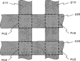
Figure 16 represents to use existing dried lithography at mask resist shown in Figure 15 219 to be carried out etching, the 3rd wiring layer 218, second metal wiring layer 215, non-volatile recording material layer 214, semiconductor layer 213, second polysilicon layer 212, first polysilicon layer 211 and insulating properties material 217 are processed, used prior art to remove resist 219 structure afterwards.At this moment, for can the selection memory unit, need residual first metal wiring layer 210 that is equivalent to the memory matrix word line.The stacked film PU1 that is made of first polysilicon layer 220, second polysilicon layer 221, semiconductor layer 222, non-volatile recording material layer 223 and second metal wiring layer 224 is a column.The 3rd metal wiring layer 226 that is equivalent to the memory matrix bit line is and the parallel longitudinal grin shape of adjacent the 3rd metal wiring layer 226, with first metal wiring layer, 210 cross-over configuration.The 3rd metal wiring layer 226 is as the bit line of memory matrix and be electrically connected with semiconductor substrate 201, thereby can carry out reading and writing of nonvolatile memory, omitted diagram at this.
Figure 17 is illustrated between the pattern of Figure 16 and has piled up after the insulating properties material, the structure after using the CMP of prior art that the insulating properties material of piling up is cut.Cutting output is the identical amount of apparent height with insulating properties material 228 and the 3rd metal wiring layer 226.
Figure 18 is illustrated in the structure of having piled up on the structure foundation of Figure 17 behind the insulating properties material 229.
The vertical view of the memory cell that will produce by the manufacture method of above use Figure 15~Figure 18 explanation is shown in Figure 19.Intersect as first metal wiring layer 210 of memory word line and the 3rd metal wiring layer 226 as bit line, stacked film PU1 is configured in its intersection point.
Below, use description of drawings to use the working method of memory matrix of the memory cell of nonvolatile memory of the present invention.
Figure 20 is the structure chart of the memory cell array of nonvolatile memory.Memory cell MCij (i=1,2,3, m) (j=1,2,3, n) structure is: first wiring (hereinafter referred to as the word line) WLi (i=1,2,3 that is configured in many configured in parallel, m) and many parellel arranged second wiring (hereinafter referred to as bit line) BLj (j=1,2,3 that intersect with word line WLi, n) intersection point selects element SE and phase change resistor element VR to be connected in series.In the figure, select the end of element SE to be connected with word line WLi, the end of phase change resistor element VR is connected with bit line BLj, but as described later, in order to apply voltage and the selection memory unit to word line WLi and bit line BLj, also can will select the end of element SE to be connected with bit line BLj, the end of phase change resistor element VR be connected with word line WLi.
The record of nonvolatile memory carries out as follows.For example, when rewrite memory unit MS11, WL1 applies voltage Vh to first word line, WLi applies voltage V1 to other word lines, BL1 applies voltage V1 to first bit line, and BLj applies voltage V1 to other bit lines, flows through electric current at the phase change resistor element of MC11 and comes stored information.At this, voltage Vh is the voltage that is higher than voltage V1.When rewriteeing,, non-selected memory cell writes the selection element SE that need play a role for not missed.Certainly, voltage Vh selects below the puncture voltage of element SE.Reading as follows of nonvolatile memory carried out.For example when the information of readout memory unit MC11, WL1 applies voltage Vm to first word line, and WLi applies voltage V1 to another word line, and BL1 applies voltage V1 to first bit line, according to the size of current sense information that flows to BL1.
Above-mentioned recorded and narrated memory matrix only be individual layer at ground floor carry out write, read, if make multilayer, further high capacity, therefore preferably.For example, as shown in figure 21, memory matrix is stacked when two-layer, on the structure foundation of Figure 18, promptly on insulating properties material 310, same with Fig. 5~Fig. 8 of embodiment 1, the second layer word line that forms memory matrix is first metal wiring layer 402, first polysilicon layer 403 by the second layer, second polysilicon layer 404 of the second layer, the semiconductor layer 405 of the second layer, the stacked film PU11 of the second layer of the column that second metal wiring layer 407 of the non-volatile recording material layer 406 of the second layer and the second layer constitutes, the 3rd metal wiring layer 409 that is equivalent to the second layer bit line of memory matrix, and form insulating properties material 408 and insulating properties material 410 gets final product.
At this moment, when the polysilicon layer of the second layer was annealed, simultaneously the non-volatile recording material layer 214 of ground floor was by overheated, but covers non-volatile recording material layer 214 by wiring layer and insulating barrier, therefore can prevent distortion, peel off.
And then the making memory matrix that when stacked k layer (k=1,2,31) memory matrix, also uses the same method.Certainly, under the situation of stacked memory matrix, need select layer at the record that carries out nonvolatile storage with when reading.About the selection of layer, for example under the shared situation of the word line of each layer, as long as select to write layer with bit line.
So, by stacked memory matrix, the bit density of memory cell uprises, and therefore can make nonvolatile storage with low cost.
In the present embodiment, memory cell of the present invention is formed on the semiconductor substrate shown in Figure 22 201.Semiconductor substrate 201 is not only to form nonvolatile memory, also be formed for making the substrate of peripheral circuit of the memory matrix work of nonvolatile memory.Use existing C MOS technology to make peripheral circuit.The position relation of peripheral circuit and memory matrix is identical with embodiment 1.
Figure 22 is illustrated in the structure of piling up first metal wiring layer 202, non-volatile recording material layer 207, semiconductor layer 206, second amorphous silicon layer 204, first amorphous silicon layer 251 on the semiconductor substrate 201 successively.First metal wiring layer 202 is formed by sputter.The material of first metal wiring layer 202 is a tungsten.Be more preferably,, can obtain read current, so the material of this first metal wiring layer 202 for example can be aluminium or copper owing to the voltage drop of the lower material of resistivity is less.In order to improve caking property, can between first metal wiring layer 202 and semiconductor substrate 201, pile up metallic compounds such as TiN.Non-volatile recording material layer 207, semiconductor layer 206 are piled up by sputter.The material of non-volatile recording material layer 207 for example is to be suitable for the Ge that utilizes crystallization-amorphous phase-change to write down
2Sb
2Te
5, thickness is 5~300nm, is more preferably the thickness of 5 low~50nm of aspect ratio, thus the dry ecthing of operation, insulating properties material imbeds after carrying out easily.Carried out the stacked stage to this, also can carry out laser annealing to the non-volatile recording material layer with semiconductor layer 206 as protective layer.At this moment, the wavelength that the laser annealing of semiconductor layer 206 is preferably used the transmission polysilicon layer is the long wavelength laser of 460nm~below the 1 μ m, but also can use the following short wavelength's of 450nm laser,, utilize heat transmission that the non-volatile recording material layer is heated so that use the polysilicon layer absorbing light.Laser radiation is Continuous irradiation or pulse irradiation.
Second amorphous silicon layer 204 obtains by utilizing LP-CVD to pile up the amorphous silicon that contains phosphorus or arsenic.Second amorphous silicon layer 204 has the thickness of 50~250nm.First amorphous silicon layer 251 obtains by utilizing LP-CVD to pile up the amorphous silicon that contains boron, gallium or indium.First amorphous silicon layer 251 has the thickness of 50~250nm.
The thickness of semiconductor layer 206 is blocked up still to be to approach all can not bring into play function.If blocked up, though conductivity is then arranged, resistance is excessive, makes the temperature surplus deficiency of the resistance value of non-volatile recording material layer 207 because of its temperature dependency.As if thin excessively, then, the storage of non-volatile recording material layer 207 can not prevent to select the deterioration in characteristics of element because writing the fashionable rising of temperature repeatedly.For above-mentioned reason, the thickness of semiconductor layer 206 is 5nm~200nm.
The material of semiconductor layer 206 is that to be difficult to take place that the rewriting condition of non-volatile recording material layer 207 changes, Ge content be the material more than 90%.It also can be embodiment 1 described material.In the present embodiment, the formation element of non-volatile recording material layer 207 is with Ge
2Sb
2Te
5Be example, also can use Ge
3Sb
2Te
6, Ge
5Sb
2Te
8, non-volatile recording material layer such as Ge-Te.Can also use the solid electrolyte material that is applicable to solid electrolyte memory record.
Figure 23 represents the operation to second amorphous silicon layer of piling up 204 and the 251 enforcement laser annealings of first amorphous silicon layer in Figure 22.Carry out the crystallization and the impurity activityization of second amorphous silicon layer 204 and first amorphous silicon layer 251 by laser annealing, thereby form second polysilicon layer 205 and first polysilicon layer 203.In the present embodiment, the selection element of formation memory cell is the pn diode.Therefore, describe, but also can use as the selection element of np knot, pin knot, pi other knots tying at memory cell with the pn knot become of first polysilicon layer 203 and second polysilicon layer 205.
If non-volatile recording material layer 207 is formed on the below of semiconductor layer 206, second amorphous silicon layer 204 and first amorphous silicon layer 251; then non-volatile recording material layer 207 is annealed by laser radiation as protective layer to major general's semiconductor layer 206; thereby reduce the disorder of the atomic arrangement of as-depo state significantly, can improve the work rate of finished products of memory component more than 10%.When polysilicon layer is annealed, the non-volatile recording material layer 207 that is positioned at its below across semiconductor layer 206 also may become the high temperature that is higher than fusing point significantly, but if anneal, then can suppress thermal diffusion downwards, prevent distortion, peel off with short wavelength's short-pulse laser.With wavelength be below the 450nm, when pulse duration is a pulsed laser irradiation below the 100 μ s, is not observing distortion, peel off.
Figure 24 is a structure of piling up second metal wiring layer 208 by sputter on the polysilicon layer of Figure 23.The material of second metal wiring layer 208 is a tungsten, but is more preferably the low aluminium of resistivity, copper.
The illustrated method of Figure 11 of Figure 25 and embodiment 1 and Figure 12 is identical, and existing photoetching technique, the dried lithography structure after on second metal wiring layer 208 shown in Figure 24 second metal wiring layer 208, first polysilicon layer 203, second polysilicon layer 205, semiconductor layer 206, non-volatile recording material layer 207 and first metal wiring layer 202 being processed is used in expression.Identical with the wordline patterns of memory matrix by first metal wiring layer 210, first polysilicon layer 211, second polysilicon layer 212, semiconductor layer 213, non-volatile recording material layer 214 with the pattern of the stacked film that second metal wiring layer 215 constitutes, be the longitudinal grin shape pattern that extends in parallel with adjacent pattern.First metal wiring layer 210 is electrically connected with semiconductor substrate 201 as the word line of memory matrix, thereby can carry out reading and writing of nonvolatile memory, has omitted diagram at this.
After the structure that Figure 26 is illustrated in Figure 25 forms, use HDP-CVD that the insulating properties material is filled between the pattern, and undertaken after the planarization, pile up the structure of the 3rd metal wiring layer 218 by existing sputter by CMP.The material of the 3rd metal wiring layer 218 is a tungsten, but is more preferably the low aluminium of resistivity, copper.
Figure 27 is illustrated in the structure that uses on the basis of Figure 26 after existing photoetching technique, dried lithography are processed the 3rd metal wiring layer 218, second metal wiring layer 215, non-volatile recording material layer 214, semiconductor layer 213, second polysilicon layer 212, first polysilicon layer 211 and insulating properties material 217.At this moment, for can the selection memory unit, need residual first metal wiring layer 210 that is equivalent to the memory matrix word line.The stacked film PU2 that is made of non-volatile recording material layer 223, semiconductor layer 222, second polysilicon layer 221, first polysilicon layer 220 and second metal wiring layer 224 is a column.The pattern of the 3rd metal wiring layer 226 is bit line patterns of memory matrix, is parallel with the adjacent bit lines pattern and longitudinal grin shape that extend.In addition, the 3rd metal wiring layer 226 is as the bit line of memory matrix and be electrically connected with semiconductor substrate 201, thereby can carry out reading and writing of nonvolatile memory, omitted diagram at this.
If with the semiconductor layer optimization, then can be after being laminated to first polysilicon layer, be that continuous laser or the pulse laser of 350nm~450nm shines first polysilicon layer and non-volatile recording material layer simultaneously with wavelength.At this moment, the material of semiconductor layer can be the Si-Ge composite material.The refractive index of Si-Ge family and the wavelength dependency of attenuation coefficient are such as shown in figure 28, therefore, the long wavelength laser that can be 460nm~1 μ m with the wavelength of transmission polysilicon layer is annealed to the non-volatile recording material layer, is that the following short wavelength laser of 350nm is annealed to polysilicon layer with wavelength then.Being more preferably, is being that the Si-Ge of 77 atom %~94 atom % makes under the situation that thickness is 5nm~200nm with containing Si, constitutes the annealing that polysilicon layer and non-volatile recording material layer all are fit to.
Figure 29 is after the structure of Figure 27 forms, and uses HDP-CVD that insulating properties material 228 is filled between the pattern, and has been undertaken after the planarization by CMP, piles up the figure of insulating properties material 229 by existing sputter.
The vertical view of the memory cell that will produce by the manufacture method of above use Figure 22~Figure 27 and Figure 29 explanation is shown in Figure 30.Intersect as first metal wiring layer 210 of memory word line and the 3rd metal wiring layer 226 as bit line, stacked film PU2 is configured in its intersection point.The employed material of each layer is identical with embodiment 1.Identical with embodiment 1, also can stacked multilayer memory matrix.
The working method of memory matrix of memory cell of having used nonvolatile memory of the present invention is identical with embodiment 1.
Identical with Fig. 5~Figure 18 of embodiment 1, the stacked film PU5 of the column that Figure 31 is illustrated on the semiconductor substrate 201 first metal wiring layer 210 that forms as the memory matrix word line, be made of first polysilicon layer 220, second polysilicon layer 221, semiconductor layer 222, non-volatile recording material layer 223, semiconductor layer 222 and second metal wiring layer 224, be equivalent to the 3rd metal wiring layer 226 of memory matrix bit line, and form insulating properties material 229 and insulating properties material 228.
By semiconductor layer is set, prevent to write the fashionable deterioration that causes by thermal cycle repeatedly at the non-volatile recording material layer, be more than 5 times but improve number of rewrites.For the total film thickness of semiconductor layer, identical with embodiment 1.The employed material of each layer is identical with embodiment 1.Identical with embodiment 1, also can stacked multilayer memory matrix.
In the present embodiment, compare, behind the formation semi-conducting material, this layer as protective layer, can be carried out laser annealing to the non-volatile recording material layer with the situation of no semiconductor layer under second metal wiring layer.For the thickness of semiconductor layer, identical with embodiment 1.The employed material of each layer is identical with embodiment 1.Identical with embodiment 1, also can stacked multilayer memory matrix.
The working method of memory matrix of memory cell of having used nonvolatile memory of the present invention is identical with embodiment 1.The position relation of peripheral circuit and memory matrix is identical with embodiment 1.
Embodiment 4
Identical with Fig. 5~Figure 18 of embodiment 1, the stacked film PU6 of the column that Figure 32 is illustrated on the semiconductor substrate 201 first metal wiring layer 210 that forms as the memory matrix word line, be made of semiconductor layer 222, non-volatile recording material layer 223, semiconductor layer 222, second polysilicon layer 221, first polysilicon layer 220 and second metal wiring layer 224, be equivalent to the 3rd metal wiring layer 226 of memory matrix bit line, and form insulating properties material 229 and insulating properties material 228.
By semiconductor layer is set, prevent to write the fashionable deterioration that causes by thermal cycle repeatedly at the non-volatile recording material layer, be more than 5 times but improve number of rewrites.For the total film thickness of semiconductor layer, identical with embodiment 1.The employed material of each layer is identical with embodiment 1.Identical with embodiment 1, also can stacked multilayer memory matrix.
The working method of memory matrix of memory cell of having used nonvolatile memory of the present invention is identical with embodiment 1.The position relation of peripheral circuit and memory matrix is identical with embodiment 1.
More than, each embodiment is described.In each embodiment, between polysilicon diode and non-volatile recording material layer, be provided with and contain the semiconductor layer of the contained element of non-volatile recording material layer, thereby the heat that can suppress to produce when impurities is because of rewriting work in the polysilicon diode is diffused into the non-volatile recording material layer.Because this semiconductor layer contains the contained element of non-volatile recording material layer, even therefore the interior Elements Diffusion of this semiconductor arrives the non-volatile recording material layer, the influence of counterweight write condition is less.Therefore, but can obtain rewriteeing the nonvolatile memory of conditional stability or number of rewrites than the more nonvolatile memory of prior art.
In each above embodiment, phase transition storage is illustrated, but only otherwise break away from thought of the present invention, just can uses known various non-volatile recording material the non-volatile recording material layer.For example be phase-change material, solid electrolyte material and magnetic material etc.At this moment,, comprise the semiconductor layer of the contained element of various materials, can obtain identical effect by setting as semi-conducting material.
Claims (12)
1. a non-volatile memory semiconductor device is characterized in that, comprising:
First electrode;
Second electrode;
Be formed on the non-volatile recording material layer between above-mentioned first electrode and above-mentioned second electrode and select element; And
Be formed on semiconductor layer between above-mentioned non-volatile recording material layer and the above-mentioned selection element, that comprise the element that above-mentioned non-volatile recording material layer comprised.
2. non-volatile memory semiconductor device according to claim 1 is characterized in that,
Above-mentioned semiconductor layer is formed on the above-mentioned selection element,
Above-mentioned non-volatile recording material layer is formed on the above-mentioned semiconductor layer.
3. non-volatile memory semiconductor device according to claim 1 is characterized in that:
Above-mentioned semiconductor layer is formed on the above-mentioned non-volatile recording material layer,
Above-mentioned selection element is formed on the above-mentioned semiconductor layer.
4. non-volatile memory semiconductor device according to claim 1 is characterized in that:
Above-mentioned non-volatile recording material layer comprises the material that contains at least a element in the chalcogen.
5. non-volatile memory semiconductor device according to claim 1 is characterized in that:
Above-mentioned semiconductor layer comprises the above Ge of 40 atom %.
6. non-volatile memory semiconductor device according to claim 5 is characterized in that:
Above-mentioned semiconductor layer comprises the above Ge of 90 atom %.
7. non-volatile memory semiconductor device according to claim 1 is characterized in that:
Above-mentioned semiconductor layer is the composite material of Ge and Si.
8. non-volatile memory semiconductor device according to claim 1 is characterized in that:
Above-mentioned semiconductor layer is InSb or GaSb.
9. non-volatile memory semiconductor device according to claim 1 is characterized in that:
Above-mentioned semiconductor layer has the thickness of 5nm~200nm.
10. non-volatile memory semiconductor device according to claim 1 is characterized in that:
Above-mentioned selection element is a diode.
11. non-volatile memory semiconductor device according to claim 10 is characterized in that:
Above-mentioned diode is a polycrystal silicon PIN diode.
12. non-volatile memory semiconductor device according to claim 1 is characterized in that:
Memory cell comprises above-mentioned non-volatile recording material layer and above-mentioned selection element,
Above-mentioned memory cell is the memory cell of phase transition storage.
Applications Claiming Priority (2)
| Application Number | Priority Date | Filing Date | Title |
|---|---|---|---|
| JP2007292723 | 2007-11-12 | ||
| JP2007292723A JP2009123725A (en) | 2007-11-12 | 2007-11-12 | Nonvolatile semiconductor storage device |
Publications (1)
| Publication Number | Publication Date |
|---|---|
| CN101436606A true CN101436606A (en) | 2009-05-20 |
Family
ID=40674792
Family Applications (1)
| Application Number | Title | Priority Date | Filing Date |
|---|---|---|---|
| CNA2008101740296A Pending CN101436606A (en) | 2007-11-12 | 2008-11-12 | Nonvolatile semiconductor memory device |
Country Status (5)
| Country | Link |
|---|---|
| US (1) | US20090140233A1 (en) |
| JP (1) | JP2009123725A (en) |
| KR (1) | KR20090049028A (en) |
| CN (1) | CN101436606A (en) |
| TW (1) | TW200939469A (en) |
Cited By (5)
| Publication number | Priority date | Publication date | Assignee | Title |
|---|---|---|---|---|
| CN104465694B (en) * | 2013-09-25 | 2018-10-09 | 爱思开海力士有限公司 | Electronic equipment |
| CN108986859A (en) * | 2017-05-30 | 2018-12-11 | 希捷科技有限公司 | Data storage device with rewritable original place memory |
| CN110335942A (en) * | 2019-07-08 | 2019-10-15 | 中国科学院上海微系统与信息技术研究所 | A kind of phase transition storage and preparation method thereof |
| US20220077261A1 (en) * | 2020-09-08 | 2022-03-10 | Samsung Display Co., Ltd. | Display device and manufacturing method thereof |
| WO2022109973A1 (en) * | 2020-11-27 | 2022-06-02 | 江苏时代全芯存储科技股份有限公司 | Manufacturing method for phase change memory, and phase change memory |
Families Citing this family (15)
| Publication number | Priority date | Publication date | Assignee | Title |
|---|---|---|---|---|
| JP2009283486A (en) * | 2008-05-19 | 2009-12-03 | Toshiba Corp | Nonvolatile storage and manufacturing method thereof |
| JP5550239B2 (en) * | 2009-01-26 | 2014-07-16 | 株式会社東芝 | Nonvolatile semiconductor memory device and manufacturing method thereof |
| JP5439147B2 (en) | 2009-12-04 | 2014-03-12 | 株式会社東芝 | Resistance change memory |
| JP5420436B2 (en) * | 2010-01-15 | 2014-02-19 | 株式会社日立製作所 | Nonvolatile memory device and manufacturing method thereof |
| US8017433B2 (en) * | 2010-02-09 | 2011-09-13 | International Business Machines Corporation | Post deposition method for regrowth of crystalline phase change material |
| JP5161911B2 (en) | 2010-03-25 | 2013-03-13 | 株式会社東芝 | Resistance change memory |
| JP5641779B2 (en) | 2010-05-18 | 2014-12-17 | 株式会社日立製作所 | Nonvolatile memory device and manufacturing method thereof |
| JP5566217B2 (en) * | 2010-07-30 | 2014-08-06 | 株式会社東芝 | Nonvolatile memory device |
| JP5674548B2 (en) * | 2011-04-28 | 2015-02-25 | 株式会社日立製作所 | Semiconductor memory device |
| CN103137646A (en) * | 2013-03-15 | 2013-06-05 | 中国科学院微电子研究所 | Strobing device unit used for cross array integration way of double-pole type resistance change storage |
| US8981334B1 (en) * | 2013-11-01 | 2015-03-17 | Micron Technology, Inc. | Memory cells having regions containing one or both of carbon and boron |
| US9876054B1 (en) | 2016-07-27 | 2018-01-23 | Western Digital Technologies, Inc. | Thermal management of selector |
| US10008665B1 (en) | 2016-12-27 | 2018-06-26 | Intel Corporation | Doping of selector and storage materials of a memory cell |
| KR102638628B1 (en) | 2017-10-20 | 2024-02-22 | 삼성전자주식회사 | Variable resistance memory device and method of forming the same |
| KR20210011638A (en) * | 2019-07-23 | 2021-02-02 | 삼성전자주식회사 | Variable resistance memory devices and methods of manufacturing the same |
Family Cites Families (2)
| Publication number | Priority date | Publication date | Assignee | Title |
|---|---|---|---|---|
| JP4491870B2 (en) * | 1999-10-27 | 2010-06-30 | ソニー株式会社 | Driving method of nonvolatile memory |
| WO2004084228A1 (en) * | 2003-03-18 | 2004-09-30 | Kabushiki Kaisha Toshiba | Phase change memory device |
-
2007
- 2007-11-12 JP JP2007292723A patent/JP2009123725A/en not_active Withdrawn
-
2008
- 2008-10-24 TW TW097140778A patent/TW200939469A/en unknown
- 2008-11-10 US US12/268,118 patent/US20090140233A1/en not_active Abandoned
- 2008-11-11 KR KR1020080111556A patent/KR20090049028A/en not_active Application Discontinuation
- 2008-11-12 CN CNA2008101740296A patent/CN101436606A/en active Pending
Cited By (7)
| Publication number | Priority date | Publication date | Assignee | Title |
|---|---|---|---|---|
| CN104465694B (en) * | 2013-09-25 | 2018-10-09 | 爱思开海力士有限公司 | Electronic equipment |
| CN108986859A (en) * | 2017-05-30 | 2018-12-11 | 希捷科技有限公司 | Data storage device with rewritable original place memory |
| CN108986859B (en) * | 2017-05-30 | 2022-04-19 | 希捷科技有限公司 | Data storage device with rewritable in-place memory |
| CN110335942A (en) * | 2019-07-08 | 2019-10-15 | 中国科学院上海微系统与信息技术研究所 | A kind of phase transition storage and preparation method thereof |
| US20220077261A1 (en) * | 2020-09-08 | 2022-03-10 | Samsung Display Co., Ltd. | Display device and manufacturing method thereof |
| US11715739B2 (en) * | 2020-09-08 | 2023-08-01 | Samsung Display Co., Ltd. | Display device and manufacturing method thereof |
| WO2022109973A1 (en) * | 2020-11-27 | 2022-06-02 | 江苏时代全芯存储科技股份有限公司 | Manufacturing method for phase change memory, and phase change memory |
Also Published As
| Publication number | Publication date |
|---|---|
| US20090140233A1 (en) | 2009-06-04 |
| KR20090049028A (en) | 2009-05-15 |
| TW200939469A (en) | 2009-09-16 |
| JP2009123725A (en) | 2009-06-04 |
Similar Documents
| Publication | Publication Date | Title |
|---|---|---|
| CN101436606A (en) | Nonvolatile semiconductor memory device | |
| CN101645453B (en) | Nonvolatile memory device and method of manufacturing the same | |
| JP6860325B2 (en) | Memory elements and semiconductor elements | |
| US9019777B2 (en) | Nonvolatile semiconductor memory device and operating method of the same | |
| CN101499437B (en) | Non-volatile memory device and method of manufacturing the same | |
| US7382647B1 (en) | Rectifying element for a crosspoint based memory array architecture | |
| US8169820B2 (en) | Use of symmetric resistive memory material as a diode to drive symmetric or asymmetric resistive memory | |
| US8288752B2 (en) | Phase change memory device capable of reducing disturbance and method of manufacturing the same | |
| JP5420436B2 (en) | Nonvolatile memory device and manufacturing method thereof | |
| CN107104122A (en) | Memory device | |
| CN1983660B (en) | Method of manufacturing non-volatile memory element | |
| KR102507303B1 (en) | Memory device | |
| CN110544742B (en) | Ferroelectric phase change hybrid storage unit, memory and operation method | |
| JP6505619B2 (en) | Super lattice memory and cross point memory device | |
| KR101177284B1 (en) | Phase change material layer and method of manufacturing the same and phase change memory device comprising phase change material layer formed using the same and methods of manufacturing and operating phase change memory device | |
| JP2022085888A (en) | Semiconductor device | |
| US8791448B2 (en) | Semiconductor memory devices having strapping contacts | |
| TWI704705B (en) | Semiconductor memory device | |
| JP2016119373A (en) | Semiconductor memorizing device and method for manufacturing the same | |
| JP2024031380A (en) | Magnetic devices and magnetic storage devices |
Legal Events
| Date | Code | Title | Description |
|---|---|---|---|
| C06 | Publication | ||
| PB01 | Publication | ||
| C10 | Entry into substantive examination | ||
| SE01 | Entry into force of request for substantive examination | ||
| C02 | Deemed withdrawal of patent application after publication (patent law 2001) | ||
| WD01 | Invention patent application deemed withdrawn after publication |
Open date: 20090520 |