CN108986859B - Data storage device with rewritable in-place memory - Google Patents
Data storage device with rewritable in-place memory Download PDFInfo
- Publication number
- CN108986859B CN108986859B CN201810537569.XA CN201810537569A CN108986859B CN 108986859 B CN108986859 B CN 108986859B CN 201810537569 A CN201810537569 A CN 201810537569A CN 108986859 B CN108986859 B CN 108986859B
- Authority
- CN
- China
- Prior art keywords
- memory
- data
- volatile memory
- selection module
- write
- Prior art date
- Legal status (The legal status is an assumption and is not a legal conclusion. Google has not performed a legal analysis and makes no representation as to the accuracy of the status listed.)
- Active
Links
Images


Classifications
-
- G—PHYSICS
- G11—INFORMATION STORAGE
- G11C—STATIC STORES
- G11C16/00—Erasable programmable read-only memories
- G11C16/02—Erasable programmable read-only memories electrically programmable
- G11C16/06—Auxiliary circuits, e.g. for writing into memory
-
- G—PHYSICS
- G11—INFORMATION STORAGE
- G11C—STATIC STORES
- G11C29/00—Checking stores for correct operation ; Subsequent repair; Testing stores during standby or offline operation
- G11C29/70—Masking faults in memories by using spares or by reconfiguring
- G11C29/78—Masking faults in memories by using spares or by reconfiguring using programmable devices
- G11C29/785—Masking faults in memories by using spares or by reconfiguring using programmable devices with redundancy programming schemes
- G11C29/789—Masking faults in memories by using spares or by reconfiguring using programmable devices with redundancy programming schemes using non-volatile cells or latches
-
- G—PHYSICS
- G06—COMPUTING; CALCULATING OR COUNTING
- G06F—ELECTRIC DIGITAL DATA PROCESSING
- G06F3/00—Input arrangements for transferring data to be processed into a form capable of being handled by the computer; Output arrangements for transferring data from processing unit to output unit, e.g. interface arrangements
- G06F3/06—Digital input from, or digital output to, record carriers, e.g. RAID, emulated record carriers or networked record carriers
- G06F3/0601—Interfaces specially adapted for storage systems
- G06F3/0602—Interfaces specially adapted for storage systems specifically adapted to achieve a particular effect
- G06F3/0614—Improving the reliability of storage systems
- G06F3/0616—Improving the reliability of storage systems in relation to life time, e.g. increasing Mean Time Between Failures [MTBF]
-
- G—PHYSICS
- G06—COMPUTING; CALCULATING OR COUNTING
- G06F—ELECTRIC DIGITAL DATA PROCESSING
- G06F12/00—Accessing, addressing or allocating within memory systems or architectures
- G06F12/02—Addressing or allocation; Relocation
- G06F12/0223—User address space allocation, e.g. contiguous or non contiguous base addressing
- G06F12/023—Free address space management
- G06F12/0238—Memory management in non-volatile memory, e.g. resistive RAM or ferroelectric memory
- G06F12/0246—Memory management in non-volatile memory, e.g. resistive RAM or ferroelectric memory in block erasable memory, e.g. flash memory
-
- G—PHYSICS
- G06—COMPUTING; CALCULATING OR COUNTING
- G06F—ELECTRIC DIGITAL DATA PROCESSING
- G06F12/00—Accessing, addressing or allocating within memory systems or architectures
- G06F12/02—Addressing or allocation; Relocation
- G06F12/08—Addressing or allocation; Relocation in hierarchically structured memory systems, e.g. virtual memory systems
- G06F12/0802—Addressing of a memory level in which the access to the desired data or data block requires associative addressing means, e.g. caches
- G06F12/0866—Addressing of a memory level in which the access to the desired data or data block requires associative addressing means, e.g. caches for peripheral storage systems, e.g. disk cache
- G06F12/0868—Data transfer between cache memory and other subsystems, e.g. storage devices or host systems
-
- G—PHYSICS
- G06—COMPUTING; CALCULATING OR COUNTING
- G06F—ELECTRIC DIGITAL DATA PROCESSING
- G06F3/00—Input arrangements for transferring data to be processed into a form capable of being handled by the computer; Output arrangements for transferring data from processing unit to output unit, e.g. interface arrangements
- G06F3/06—Digital input from, or digital output to, record carriers, e.g. RAID, emulated record carriers or networked record carriers
- G06F3/0601—Interfaces specially adapted for storage systems
- G06F3/0602—Interfaces specially adapted for storage systems specifically adapted to achieve a particular effect
- G06F3/061—Improving I/O performance
- G06F3/0611—Improving I/O performance in relation to response time
-
- G—PHYSICS
- G06—COMPUTING; CALCULATING OR COUNTING
- G06F—ELECTRIC DIGITAL DATA PROCESSING
- G06F3/00—Input arrangements for transferring data to be processed into a form capable of being handled by the computer; Output arrangements for transferring data from processing unit to output unit, e.g. interface arrangements
- G06F3/06—Digital input from, or digital output to, record carriers, e.g. RAID, emulated record carriers or networked record carriers
- G06F3/0601—Interfaces specially adapted for storage systems
- G06F3/0628—Interfaces specially adapted for storage systems making use of a particular technique
- G06F3/0655—Vertical data movement, i.e. input-output transfer; data movement between one or more hosts and one or more storage devices
- G06F3/0656—Data buffering arrangements
-
- G—PHYSICS
- G06—COMPUTING; CALCULATING OR COUNTING
- G06F—ELECTRIC DIGITAL DATA PROCESSING
- G06F3/00—Input arrangements for transferring data to be processed into a form capable of being handled by the computer; Output arrangements for transferring data from processing unit to output unit, e.g. interface arrangements
- G06F3/06—Digital input from, or digital output to, record carriers, e.g. RAID, emulated record carriers or networked record carriers
- G06F3/0601—Interfaces specially adapted for storage systems
- G06F3/0628—Interfaces specially adapted for storage systems making use of a particular technique
- G06F3/0655—Vertical data movement, i.e. input-output transfer; data movement between one or more hosts and one or more storage devices
- G06F3/0659—Command handling arrangements, e.g. command buffers, queues, command scheduling
-
- G—PHYSICS
- G06—COMPUTING; CALCULATING OR COUNTING
- G06F—ELECTRIC DIGITAL DATA PROCESSING
- G06F3/00—Input arrangements for transferring data to be processed into a form capable of being handled by the computer; Output arrangements for transferring data from processing unit to output unit, e.g. interface arrangements
- G06F3/06—Digital input from, or digital output to, record carriers, e.g. RAID, emulated record carriers or networked record carriers
- G06F3/0601—Interfaces specially adapted for storage systems
- G06F3/0668—Interfaces specially adapted for storage systems adopting a particular infrastructure
- G06F3/0671—In-line storage system
- G06F3/0673—Single storage device
- G06F3/0679—Non-volatile semiconductor memory device, e.g. flash memory, one time programmable memory [OTP]
-
- G—PHYSICS
- G11—INFORMATION STORAGE
- G11C—STATIC STORES
- G11C11/00—Digital stores characterised by the use of particular electric or magnetic storage elements; Storage elements therefor
- G11C11/005—Digital stores characterised by the use of particular electric or magnetic storage elements; Storage elements therefor comprising combined but independently operative RAM-ROM, RAM-PROM, RAM-EPROM cells
-
- G—PHYSICS
- G11—INFORMATION STORAGE
- G11C—STATIC STORES
- G11C16/00—Erasable programmable read-only memories
- G11C16/02—Erasable programmable read-only memories electrically programmable
- G11C16/06—Auxiliary circuits, e.g. for writing into memory
- G11C16/10—Programming or data input circuits
-
- G—PHYSICS
- G11—INFORMATION STORAGE
- G11C—STATIC STORES
- G11C16/00—Erasable programmable read-only memories
- G11C16/02—Erasable programmable read-only memories electrically programmable
- G11C16/06—Auxiliary circuits, e.g. for writing into memory
- G11C16/26—Sensing or reading circuits; Data output circuits
-
- G—PHYSICS
- G06—COMPUTING; CALCULATING OR COUNTING
- G06F—ELECTRIC DIGITAL DATA PROCESSING
- G06F2212/00—Indexing scheme relating to accessing, addressing or allocation within memory systems or architectures
- G06F2212/10—Providing a specific technical effect
- G06F2212/1016—Performance improvement
-
- G—PHYSICS
- G06—COMPUTING; CALCULATING OR COUNTING
- G06F—ELECTRIC DIGITAL DATA PROCESSING
- G06F2212/00—Indexing scheme relating to accessing, addressing or allocation within memory systems or architectures
- G06F2212/21—Employing a record carrier using a specific recording technology
- G06F2212/211—Optical disk storage
-
- G—PHYSICS
- G06—COMPUTING; CALCULATING OR COUNTING
- G06F—ELECTRIC DIGITAL DATA PROCESSING
- G06F2212/00—Indexing scheme relating to accessing, addressing or allocation within memory systems or architectures
- G06F2212/21—Employing a record carrier using a specific recording technology
- G06F2212/214—Solid state disk
-
- G—PHYSICS
- G06—COMPUTING; CALCULATING OR COUNTING
- G06F—ELECTRIC DIGITAL DATA PROCESSING
- G06F2212/00—Indexing scheme relating to accessing, addressing or allocation within memory systems or architectures
- G06F2212/72—Details relating to flash memory management
- G06F2212/7203—Temporary buffering, e.g. using volatile buffer or dedicated buffer blocks
-
- G—PHYSICS
- G11—INFORMATION STORAGE
- G11C—STATIC STORES
- G11C2207/00—Indexing scheme relating to arrangements for writing information into, or reading information out from, a digital store
- G11C2207/10—Aspects relating to interfaces of memory device to external buses
- G11C2207/102—Compression or decompression of data before storage
-
- G—PHYSICS
- G11—INFORMATION STORAGE
- G11C—STATIC STORES
- G11C2207/00—Indexing scheme relating to arrangements for writing information into, or reading information out from, a digital store
- G11C2207/22—Control and timing of internal memory operations
- G11C2207/2245—Memory devices with an internal cache buffer
-
- G—PHYSICS
- G11—INFORMATION STORAGE
- G11C—STATIC STORES
- G11C2207/00—Indexing scheme relating to arrangements for writing information into, or reading information out from, a digital store
- G11C2207/22—Control and timing of internal memory operations
- G11C2207/2272—Latency related aspects
-
- G—PHYSICS
- G11—INFORMATION STORAGE
- G11C—STATIC STORES
- G11C7/00—Arrangements for writing information into, or reading information out from, a digital store
- G11C7/10—Input/output [I/O] data interface arrangements, e.g. I/O data control circuits, I/O data buffers
- G11C7/1006—Data managing, e.g. manipulating data before writing or reading out, data bus switches or control circuits therefor
-
- G—PHYSICS
- G11—INFORMATION STORAGE
- G11C—STATIC STORES
- G11C7/00—Arrangements for writing information into, or reading information out from, a digital store
- G11C7/10—Input/output [I/O] data interface arrangements, e.g. I/O data control circuits, I/O data buffers
- G11C7/1078—Data input circuits, e.g. write amplifiers, data input buffers, data input registers, data input level conversion circuits
- G11C7/1084—Data input buffers, e.g. comprising level conversion circuits, circuits for adapting load
-
- G—PHYSICS
- G11—INFORMATION STORAGE
- G11C—STATIC STORES
- G11C7/00—Arrangements for writing information into, or reading information out from, a digital store
- G11C7/18—Bit line organisation; Bit line lay-out
-
- G—PHYSICS
- G11—INFORMATION STORAGE
- G11C—STATIC STORES
- G11C8/00—Arrangements for selecting an address in a digital store
- G11C8/14—Word line organisation; Word line lay-out
-
- Y—GENERAL TAGGING OF NEW TECHNOLOGICAL DEVELOPMENTS; GENERAL TAGGING OF CROSS-SECTIONAL TECHNOLOGIES SPANNING OVER SEVERAL SECTIONS OF THE IPC; TECHNICAL SUBJECTS COVERED BY FORMER USPC CROSS-REFERENCE ART COLLECTIONS [XRACs] AND DIGESTS
- Y02—TECHNOLOGIES OR APPLICATIONS FOR MITIGATION OR ADAPTATION AGAINST CLIMATE CHANGE
- Y02D—CLIMATE CHANGE MITIGATION TECHNOLOGIES IN INFORMATION AND COMMUNICATION TECHNOLOGIES [ICT], I.E. INFORMATION AND COMMUNICATION TECHNOLOGIES AIMING AT THE REDUCTION OF THEIR OWN ENERGY USE
- Y02D10/00—Energy efficient computing, e.g. low power processors, power management or thermal management
Abstract
A data storage device may have at least a buffer memory, a selection module, and a non-volatile memory. The buffer memory and the non-volatile memory may be comprised of different types of memory, while the non-volatile memory has one or more rewritable in-place memory cells. The buffer memory and non-volatile memory may each store data associated with pending data requests as indicated by the selection module until the dwell time of the rewritable in-place memory unit has expired.
Description
Disclosure of Invention
According to various embodiments, a data storage device has a buffer memory, a selection module, and a non-volatile memory. The buffer memory and the non-volatile memory are comprised of different types of memory, while the non-volatile memory has one or more rewritable in-place memory cells. The buffer memory and the non-volatile memory each store data associated with pending data requests as indicated by the selection module until the dwell time for the rewritable in-place memory unit has expired.
Drawings
FIG. 1 shows a block diagram of an example data storage system in which various embodiments may be implemented.
FIGS. 2A and 2B respectively illustrate portions of an example data storage device that may be used in the data storage system of FIG. 1.
Fig. 3A-3C depict portions of an example memory unit that may be used in the data storage system of fig. 1, respectively.
FIG. 4 depicts example operational data associated with the data storage system of FIG. 1.
Fig. 5A and 5B illustrate portions of an example data storage device, respectively, operating in accordance with various embodiments.
FIG. 6 illustrates a block diagram of portions of an example data storage device, arranged in accordance with some embodiments.
Fig. 7 is a block diagram of portions of an example data storage device configured in accordance with various embodiments.
FIG. 8 shows a block diagram of a portion of an example data storage device that may be used with the data storage system of FIG. 1.
Fig. 9 depicts a block diagram of a portion of an example data storage device, arranged in accordance with some embodiments.
Figures 10A-10D each represent a portion of an example lithographic assembly formed in accordance with various embodiments.
FIG. 11 is a flow diagram of an example in-place memory utilization routine performed with the data storage system of FIG. 1, according to some embodiments.
Detailed Description
As more and more data is generated, transmitted, and stored, the speed, cost, size, and longevity of data storage becomes increasingly stressed. Although Hard Disk Drives (HDDs) that employ gyromagnetic media are capable of reliably storing data for long periods of time, HDDs are precluded from use in many computing devices due to their relatively large physical size and slow data access speeds. Solid state drives, which employ NAND flash memory, can provide faster data access speeds and smaller physical size than HDDs, but at higher cost and with shorter lifetimes.
The relatively short life of flash memory is exacerbated by data management structures and schemes that repeatedly write, move, and delete data in an effort to reduce data access latency. The fact that flash memory is not bit-addressable or byte-addressable, but only page/sector-addressable, shortens the lifetime of the memory and results in complex data management and relatively longer data access times compared to bit-addressable/byte-addressable volatile memory. However, requiring volatile memory to be continuously capable of retaining data may limit the potential applicability of these types of memory in data storage devices.
Thus, various embodiments are generally directed to data storage structures and operations utilizing rewritable in-place memory that enjoys faster data access speeds than flash memory, smaller physical size and nonvolatile data retention than HDDs. Being able to store data in non-volatile memory at relatively fast data access speeds would allow a wide variety of data management structures and schemes to optimize data retention, reading, and writing. At the same time, the relatively small physical size of rewritable in-place memory allows data storage devices to be small enough to be implemented in modern computing devices such as smartphones and tablets, while being robust enough to be used in large data capacity centers.
FIG. 1 shows an example data storage system 100 in which various embodiments of the present disclosure may be implemented. The system 100 may connect any number of data storage devices 102 to any number of hosts 104 via a wired and/or wireless network. The one or more network controllers 106 may be hardware or software based and provide data request processing and distribution to the various data storage devices 102 connected. It should be noted that the plurality of data storage devices 102 may be similar or dissimilar types of memory having different data capacities, operating parameters, and data access speeds.
In some embodiments, at least one data storage device 102 of the system 100 has a local processor 108, such as a microprocessor or programmable controller, connected to an on-chip buffer 110, such as a Static Random Access Memory (SRAM), and an off-chip buffer 112, such as a Dynamic Random Access Memory (DRAM), and a non-volatile memory array 114. The non-limiting embodiment of fig. 1 arranges a non-volatile memory array 114 that includes NAND flash memory, shown schematically in part as where a first bit line (BL1) and a second bit line (BL2) operate with a first word line (WL1) and a second word line (WL2) and a first source line (SL1) and a second source line (SL2) to write and read data stored in first flash cell 116, second flash cell 118, third flash cell 120, and fourth flash cell 122.
It should be noted that the respective bit lines correspond to a first memory page 124 and a second memory page 126, which are the minimum resolution of the memory array 114. That is, the construction of flash memory prevents flash cells from being individually re-writable in place, but page by page. Such low data resolution and the fact that flash memory is exhausted after multiple write/rewrite cycles corresponds to multiple performance bottlenecks and operational inefficiencies compared to memories where cells are bit addressable while being individually accessible and rewritable in place. Thus, various embodiments relate to implementing bit-addressable rewritable in-place memory as a data storage device 102, which may be part of a distributed network data storage system 100.
Fig. 2A and 2B illustrate portions of an example storage array 140 that may be used in a data storage device, according to various embodiments. Memory array 140 has a plurality of individual memory cells 142 that are vertically stacked along the Z-axis as part of a three-dimensional array. While it is contemplated that a single chip of memory unit 142 may be utilized, such a configuration has resulted in reduced data capacity and failed to utilize all available space. Thus, various implementations vertically stack multiple chips of memory cells 142, each residing on an X-Y plane. However, the vertically stacked units 142 do not necessarily need to be vertically aligned in the manner shown in fig. 2A.
In the case of NAND flash memory and other solid state data storage cells, transistors or other separate selection components are incorporated into each cell, which consumes valuable resources, consumes additional power, and increases the latency of data access operations. Each memory cell 142 of memory array 140 is constructed without a transistor or other physically separate selection component, but rather with a selection layer 144 in contact with a resistive element 146. The selection layer 144 may be a single material or a stack of different materials to prevent current from flowing to the resistance unit 146 at a predetermined time and to allow current to flow to the resistance unit 146 at other predetermined times. As non-limiting examples, the selection layer 144 may be a metal-insulator transition (MIT) material, an Ovonic Threshold Switch (OTS), or other voltage regulating structure.
As shown in fig. 1, the inclusion of a transistor or other selection component corresponds to the source line that activates the respective selection component. The elimination of any select components that facilitate selection of layer 144 allows vertically stacked memory cells 142 to be individually accessible through a cross-point interconnect configuration, where Bit Lines (BL) operate with Word Lines (WL) to access one or more cells 142. The potential difference induced between the bit line and the word line causes a current to flow through the individual memory cell 142, as shown by line 148. Being able to select a single bit (and thus bit-addressable) would allow memory array 140 to densely pack cells without fear of inadvertently accessing memory cells 142.
It should be noted that the construction of the memory cells 142 provides a relatively low power consumption, which corresponds to a low risk of interference for non-selected and physically adjacent cells 142 during read and/or write operations. The top view of fig. 2B conveys how memory cells 142 may be positioned along a single chip relative to various bit lines and word lines. By utilizing bit lines between vertically stacked memory cells 142, the total number of control interconnects may be reduced, which provides a more densely packed memory array 140.
Fig. 3A-3C convey line representations, respectively, of example non-volatile resistive cells that can be used for memory array 140. Fig. 3A shows a phase-change resistive cell 160 with a resistive region 162 occupied by a chalcogenide glass material 164 that reacts to current to transition between an amorphous state 166, a low resistance state, and a crystalline high resistance state. Switching between the polycrystalline and amorphous states can be reliably and efficiently cycled. However, for phase change resistance cell 160, the write/switch current may be relatively high.
Fig. 3B shows a filament-type resistive cell 170 in which the resistive region 162 includes a material having a high resistance until one or more conductive filaments 172 are initiated by a write current flowing through the region 162. Filament formation may be simple and effective, but it is contemplated that the filaments may be entrained in the dielectric material 174 and reduce the margin between the high resistance state and the low resistance state.
The formation of conductive paths in phase-change resistive element 160 and filamentary resistive element 170 may be effective in some data storage arrangements, but not necessarily the entire memory array. Thus, the resistive unit may produce different resistance states via relative magnetic orientation. The magnetoresistive cell 180 of FIG. 3C shows how the dielectric spacer layer 182 is disposed between the magnetic free layer 184 and the magnetic reference layer 186. The reference layer 186 is disposed at a fixed magnetization 188, while the free layer 184 may be disposed at a plurality of different magnetic orientations 190 that provide different resistance states for the cell 180 relative to the fixed magnetization 188. It is contemplated that the resistive unit 180 may have an additional spin polarizing layer, such as in a spin torque arrangement, for making the switching of the free magnetization 188 more efficient.
Being able to utilize different types of resistive cells in a memory array allows the data storage device to customize the operation and data storage capabilities of the data storage device. As a non-limiting example, a memory array may employ different types of resistive cells on different chips, which may provide a selectable variety of operating conditions and data storage parameters. Regardless of the type or variety of resistive cells in a memory array, memory cells may suffer from asymmetric accesses, where the time taken to complete a write operation is different than a read operation. That is, replacing a separate selection component (such as a transistor or diode) for selection layer 144 may result in asymmetric access. Such asymmetric access can create problems in data storage devices in which a large number of data write and read operations can be performed without worrying about or evaluating whether a previous read or write operation was completed.
For a memory array employing phase-change resistive cell 160, it should be noted that more time may be required to complete a write access than to read, e.g., a read latency of 7 microseconds and a write latency of 10+ microseconds. It is envisaged that the read/write asymmetry may be even larger, e.g. two times or even more than an order of magnitude, when the write operation is completed, compared to the read operation. These problems create interesting data management situations that are not addressed in volatile memory, HDD storage, or NAND flash storage.
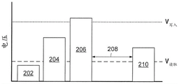
FIG. 4 depicts example operational data over time of voltages associated with a memory array employing asymmetric memory cells, in accordance with various embodiments. The construction of the memory cells of the memory array corresponds to different read threshold voltages (V)Reading) And a write threshold voltage (V)Writing in) To access or modify the memory cell resistance state and associated binary state, respectively.
In the event that the first voltage 202 received by one or more memory cells is below both the read and write threshold voltages, the select layer of each memory cell will prevent the voltage from passing through the cell, which could prevent inadvertent resistance changes from weakening the data access operation. When voltage 204/206 is greater than the read threshold voltage, the select layer of the memory cell allows the voltage to pass through the cell. For a voltage 204 insufficient to change the resistance state of the resistive cell, the existing resistance state will be read via signals through the orthogonally oriented bit and word lines.
The write voltage 206 through the memory cell will change the resistive state of the resistive cell. However, there is a dwell time 208 after the write voltage passes through the resistive cell for setting the memory cell to a resistive state that is accessible with a read voltage 210. The dwell time 208 directly causes the read/write asymmetry of the memory cell as shown in fig. 4. Thus, the relatively high data capacity and fast read latency associated with the memory array 140 may be reduced due to write asymmetry, which requires the data storage device to monitor and account for the relatively long dwell time of each memory cell for each instance a cell is written.
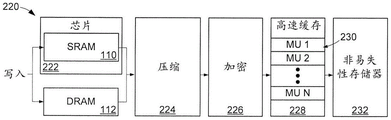
Accordingly, various embodiments relate to structures and methods to optimize the use of the non-volatile, bit-addressable, rewritable in-place memory of FIG. 2 that is subject to asymmetric read/write operations. Fig. 5A and 5B convey block diagrams of example write and read operations, respectively, for a data storage device 220 having the memory array of fig. 2. The write operation is shown in FIG. 5A and begins with: the data of the write request flows to the SRAM buffer 110 located on the wafer chip 222 and/or the DRAM buffer 112 located off the chip 222. The write data is then sequentially compressed 224 and encrypted 226 as directed by the local controller performing firmware, software, or hardware operations.
The compressed and encrypted write data is compiled in write cache 228 as a Memory Unit (MU)230 that may be comprised of multiple pages and/or sectors of data. It should be noted that for rewritable in-place non-volatile memory, since the various bits are accessible, the MU 230 does not need to be compiled, as opposed to page-accessible flash memory. Regardless of whether the write data is organized into mapping units 230, the write cache 228 may temporarily store the write data until the data is written to non-volatile MEMORY (NV MEMORY)232, where at least a portion of the MEMORY 232 has asymmetric MEMORY cells 142 of fig. 2.
As data is written to the asymmetric cells of the non-volatile memory 232, the read operation cannot reliably access the data from the non-volatile memory 232 until after the dwell time 208. Thus, in some embodiments, the read operation involves the selection module 234 of the data storage device retrieving data from the write cache 228 or the non-volatile memory 232, as shown in FIG. 5B. It should be noted that write cache 228 is a different type of memory than non-volatile memory 232, such as DRAM or NAND flash, and that read operations will involve decryption and decompression before being sent to the host. Thus, the selection module 234 intelligently manages the many different types of memory to take advantage of the fast read speed of the non-volatile memory cells 142 of FIG. 2 without suffering extended write delays due to the dwell time of the cells 142.
Although not limiting or required, the selection module 234 may perform various intelligent evaluations to optimize the satisfaction of data access from one or more hosts. FIG. 6 is a block diagram of a portion of an example data storage device 240 employing the memory array 140 of FIG. 2. The selection module 234 may access at least one timer 242, an activity log 244, sensors 246, and prediction circuitry 248 to evaluate the optimal destination and conditions for a write or read request to be used.
At any time after receiving a write or read request from the host, the selection module 234 may evaluate the current state of the individual data storage devices as well as the entire data storage system. While the selection module 234 may evaluate any type and number of inputs simultaneously and/or sequentially, in particular, some embodiments receive the status of pending writes in the write queue, which may be the capacity, size, and buffer characteristics of the data associated with the pending write requests. The selection module 234 may further receive system performance metrics such as power consumption, average data access latency, and bit error rate.
The specified write location of the pending write and the data version provide biographical information about the pending data write to the selection module 234. Any number and type of environmental conditions may be polled and/or detected with the sensors 246 to identify any potentially adverse data access conditions. For example, temperature detector 246 may be used to verify the temperature within the data storage device as compared to the polled ambient temperature received from the remote host. Other environmental conditions such as humidity, vibration, and airflow may also be polled and/or sensed to provide a more comprehensive status of the data storage device and system.
The selection module 234 may record the execution and system conditions associated with the service data access request. The collection of information related to previously serviced data access requests allows the selection module 234 to react more intelligently to system conditions and proactively initiate actions to optimize servicing of future data access requests. That is, the selection module 234 may utilize current device/system conditions as well as data from the log 244 to intelligently identify passive and active actions that may optimize pending read and write request servicing. Thus, the selection module 234 may reactively move data between the volatile buffer and the non-volatile memory, change write locations, and change read locations.
The operational state of the data storage device and system can be evaluated and determined to intelligently perform actions for servicing pending data access requests, allowing the data storage device to adapt to changing conditions and service requests as quickly as possible. With respect to asymmetric rewritable in-place memory, the selection module 234 may write the risk of read requests for data within a dwell time to non-volatile memory with less intelligence, hold the data in a buffer/cache memory to service the read request, and move the data to a different buffer/cache location to provide the lowest read latency.
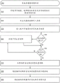
In the case where the selection module 234 actively takes action to optimize the servicing of pending data requests, it may be difficult to discern the current location of valid data without a robust mapping scheme. However, mapping Logical Block Addresses (LBAs) to Physical Block Addresses (PBAs) and LBA to LBA can be expensive in terms of processing and data capacity, particularly in on-chip SRAM buffers. With redundant retention of data at two different locations, the mapping may become more complex to service read requests for data during the dwell time. Thus, for LBA to PBA and LBA to LBA mapping operations, some embodiments utilize the selection module 234 to specify storage locations and processing times.
FIG. 7 illustrates a block diagram of an example mapping scheme 250 that may be implemented in a data storage device employing the memory array 140 of FIG. 2. The presence of multiple different types of memory in the data storage device allows the selection module 234 to generate multiple different data maps to optimize the capabilities and current state of the respective types of memory.
In the non-limiting example shown in FIG. 7, the selection module 234 may create a first level mapping 252 in a first type of memory 254, such as volatile DRAM, SRAM, or non-volatile flash memory. In some embodiments, the first level mapping 252 includes at least one LBA to PBA launch mapping that contains entries pointing to granules consisting of 12 entries. The first level mapping 252 may generally direct the controller to a logical or physical location of the second level mapping 256, where the LBA to PBA transitions are included at a higher resolution than the first level mapping 252. That is, second level mapping 256 may include a local entry pointing to the first granule that holds the host-provided data sector. Data reads, writes, and updates may be efficiently handled as a result of the first-level mapping 252 and the second-level mapping 256.
The selection module 234 may create a separate shadow map 258 in the first type of memory 254 that contains information about the temporal location of the shadow data. It should be understood that shadow data is data that is redundantly stored for a short period of time until the data permanently resides in non-volatile memory. Shadow map 258 may be simple or complex, with one or more versions of data identified. For example, shadow map 258, first level map 252, and second level map 256 may track successive versions of data to ensure that the most recent version of data is retrieved by a read request for the data. It should be noted that the shadow map 258 and the level map 252/256 may be written, read, and updated simultaneously by a common or distinct controller.
The data tracked by shadow map 258 and level map 252/256 is ultimately written to master data store 260, which is a bit-addressable rewritable in-place memory 262. As shown, the master data store 260 and the second-level mapping 256 are each stored in non-volatile rewritable in-place memory 262. However, such a configuration is not required or limiting, as any amount and type of memory may be used for the corresponding mapping 252/256/258. For example, the first level mapping 252 may be stored in serial NOR flash, the shadow mapping 258 is stored in clustered SRAM, and the second level mapping 256 is stored in DDR DRAM. The use of at least two different types of memory 254/262 allows the selection module 234 to intelligently generate and maintain various mappings 252/256/258 in memory that most efficiently allow data read and write requests to be serviced.
It is contemplated that the selection module 234 may vary the size, purpose, and storage location of the various mappings 252/256/258 to accommodate changing system and device conditions. The selection module 234 may further change the memory and/or mapping via virtualization. That is, selection module 234 may create virtual machines that, while located in common memory 254/256, run independently in software/firmware. Such virtualization capabilities allow the selection module 234 to adapt in real-time to detected and/or predicted system and device conditions to optimize data read and write latency.
Fig. 8 illustrates a block diagram of a portion of an example data storage device 270 employing virtualization of memory, in accordance with various embodiments. One or more different write caches 272 may feed into non-volatile memory 274, which includes bit-addressable rewritable in-place memory such as array 140. While data storage 270 may be comprised of multiple separate non-volatile memories 274, some embodiments include a single non-volatile memory 274 logically divided into different memory hierarchies, which may be referred to as virtualized storage.
As indicated by the solid-line arrows, data may flow between any virtualization layer levels as directed by the selection module and/or the local controller. For example, data may move continuously through the respective levels 276/278/280/282 depending on the amount of update activity, which results in the least accessed data residing in the fourth level 282 and the most frequently updated data residing in the first level 276. Another non-limiting example involves initially placing the data in a first level 276 and then moving the data to other, possibly non-contiguous levels to allow more efficient storage and retrieval, such as based on data size, security, and/or host origin.
It will be appreciated that the rewritable in-place memory of non-volatile memory 274 allows for adaptive virtualization of the corresponding hierarchy 276/278/280/282. That is, the ability to write data to specific bits, bytes, and sectors without having to store unselected data for a common page allows the virtualization hierarchy to have varying sizes, distributed content, and existence based on system and device requirements determined by the selection module 234. Thus, the virtualization scheme of FIG. 8 may be changed over time by the selection module 234 in any manner to optimize data storage for real-time conditions of the data storage system and devices.
The virtualization of portions of non-volatile memory 274 is supplemented by the ability of selection module 234 to take proactive action to satisfy predicted data storage activities and/or operational events. Fig. 9 depicts a block diagram of a portion of an example data storage device 290 employing a selection module 234 having prediction circuitry 248, operating in accordance with various embodiments. The prediction circuit 248 may detect and/or poll a wide variety of information regarding current and past data storage operations and environmental conditions during those operations. It should be noted that the prediction circuit 248 may utilize one or more real-time sensors 246 of the selection module 234 to detect one or more different environmental conditions, such as device operating temperature, ambient temperature, and power consumption.
In the event one or more parameters are input simultaneously and/or sequentially, as shown in FIG. 9, the prediction circuit 248 may predict the occurrence of future events that may be accommodated as indicated by the selection module 234. For example, the selection module 234 may modify data such as data size, location, and security to accommodate predicted events. In another non-limiting example, the selection module 234 may direct redundant writes of shadow data to one or more locations other than the non-volatile memory, which may provide for efficient data reads when the non-volatile memory is within its dwell time.
Although not exhaustive, the prediction circuit 248 may receive information about the current state of the write queue, such as the capacity and size of each pending write request in the queue. The prediction circuit 248 may also poll or determine any number of system/device performance metrics, such as write delay, read delay, and error rate. The prediction circuit 248 may evaluate the version of data pending or being written to determine the update frequency of the data. The prediction circuit 248 may utilize the allocated write locations of pending and previously completed data writes to perform wear leveling operations in the non-volatile memory.
One or more environmental conditions may be sensed and/or polled in real time by the prediction circuit 248 to determine trends and conditions that may be indicative of future data storage activity. The availability of space in one or more shadow buffers (e.g., SRAM or NOR flash) may identify the performance of the buffers to the prediction circuit 248 and indicate the system's ability to process future pending write requests. The prediction circuit 248 may employ one or more algorithms 292 and at least one log 294 of previous data storage activity to predict events and adjust actions that may optimize the servicing of read and write requests.
It is contemplated that log 294 includes previously recorded and externally modeled events, actions, and system conditions. The recorded information is useful to the selection module 234 in determining the accuracy of the predicted event and the effectiveness of the proactive action. Such self-evaluation may be used to update the algorithm 292 to improve the accuracy of the predicted event. By determining the accuracy of the previous predicted event, the prediction module 248 may assess the risk that the predicted action will occur and/or the opportunity to adjust the action will optimize system performance. This capability allows the prediction module 248 to operate relative to the threshold established by the selection module 234 to ignore predicted events and proactive actions that are unlikely to improve system performance, such as 95% confidence that an event will occur or 90% chance that a proactive action improves system performance.
By ignoring the unlikely ability to predict events and proactive actions, the selection module 234 can generate many different scenarios simultaneously and sequentially, for example, using different algorithms 292 and/or logs 294. As a non-limiting example, the prediction circuit 248 may be responsible for predicting events and corresponding corrective actions based on separate modeling logs, separate real-time system conditions, and a combination of modeling and real-time information. Thus, the prediction circuit 248 and the selection module 234 may evaluate system conditions to produce reactive and proactive actions that have a high chance of improving the servicing of current and future data access requests to the data storage device.
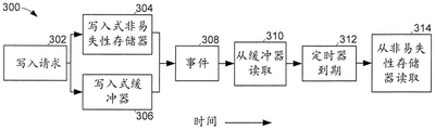
Fig. 10A-10D convey example operating scenarios, respectively, that result from intelligent operation of the selection module 234 over time. FIG. 10A shows a scheme 300 in which a pending write request 302 is simultaneously written to non-volatile memory in step 304 and at least one write buffer in step 306. The actual event or predicted event in step 308 may trigger the selection module 234 to read data from the buffer in step 310 until the timer expires in step 312. In other words, the redundant writing of data allows data to be read from the buffer while the non-volatile memory is at its dwell time in step 310, and then read from the non-volatile memory in step 314.
In scheme 300, the event of step 308 may be longer than the average dwell time, which may be due to device temperature or other operating conditions that require reading data during the dwell time of the non-volatile memory. For example, in step 308, a write to a multi-level non-volatile memory unit or a predicted likelihood of data that the host requests a recent write may prompt the selection module 234 to direct data retrieval from the temporary buffer. It is contemplated that the timer of step 312 may be used for a dwell time of the non-volatile memory or a specified delay time as determined by the selection module 234 to more efficiently service the data access request than if no delay was present.
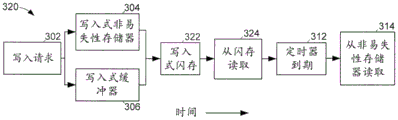
FIG. 10B shows an example scenario 320 in which the write request of step 302 and the writing of data to both the non-volatile memory and the buffer are the same as scenario 300. However, no actual or predicted event occurs in step 322 but data is written to flash memory and then read from memory in step 324 until the timer expires in step 312, and then data is read from non-volatile memory in step 314. The use of flash memory in steps 322 and 324 may partially or completely empty the write buffer, which may allow a faster write buffer to service other pending system activities.
Some embodiments predict an unplanned loss or reduction in power to the data storage device/system, which triggers the selection module to send all data from the volatile buffer to the non-volatile memory. Other embodiments respond to a predetermined power reduction by sending all data to the rewritable in-place non-volatile memory, such as shutting down the device/system. Since the dwell time of the non-volatile memory need not be taken into account during shutdown, the selection module can dump a large amount of data to the non-volatile memory without harm.
The relatively fast read time of a rewritable in-place memory can be intelligently employed during scheduled shutdown by storing one or more boot maps to non-volatile memory. It should be noted that the selection module 234 may generate a new boot map based on current and recent system activity to provide a near instantaneous boot process, where the boot map is loaded exclusively from non-volatile memory and then moved to other memory where updates are performed more efficiently. By sending existing or newly generated startup data (e.g., security information, level mapping, and firmware), the data storage device/system may be ready to receive new data access requests in less than 1 second of power initialization.
Turning to FIG. 10D, a scheme 340 processes the write request from step 302 by simultaneously and redundantly writing to non-volatile memory in step 304 and writing to a buffer in step 306. While the write to the non-volatile memory dwells, step 310 services any reads from the buffer until the selection module 234 timer in step 312 expires. The predicted or encountered event in step 342 triggers the selection module 234 to continue servicing data read requests from the buffer rather than from the non-volatile memory, even though the data write to the non-volatile memory has stalled. The event in step 342 is not limited, but may be any operating condition that may prevent or weaken the reading of data from the non-volatile memory, such as an error, high device/system processing activity, or channel availability.
It is contemplated that the selection module 234 may handle the overwrite condition during the dwell time of the memory cell. In this case, "Dirty" and "writelnprogress" flags are added to the cache entry. Although not required or limited, the Dirty flag indicates that the data in the cache has not been written to the non-volatile memory, and the WriteInProgress flag indicates that the data in the cache has been written to the non-volatile memory, but the cool-down period has not been completed. Thus, the selection module 234 can intelligently assess whether the data is currently in a dwell phase, which reduces redundant operations and improves system performance.
10A-10D, it can be appreciated that the selection module 234 can take various actions to adapt to predicted and/or actual events to optimize the servicing of data access requests. This intelligent adaptation allows the selection module to maintain a high data access bandwidth and low data access latency regardless of the amount of data access. Intelligent adaptation further allows the selection module to alter the data storage locations, mapping schemes, and writing of shadow data to accommodate changes in data priority and security, which can send very important data to non-volatile data faster.
Fig. 11 is a flow diagram of an example in-place memory utilization routine 350 that may be performed by the various embodiments of fig. 1-10D. One or more data storage devices, each of which is comprised of a selection module, a buffer module, and a rewritable in-place non-volatile memory, may be activated in step 352. The data storage device may be run for any time as part of a distributed network in a data storage system. When the at least one data storage device receives one or more data write requests from the host in step 354, the selection module may write data associated with the pending data request to the at least one buffer memory and the non-volatile memory in step 356.
The programming of the write data to the buffer and non-volatile memory in step 356 may be done simultaneously or sequentially. However, when data is written to non-volatile memory, the selection module starts a timer to determine when the memory cell has completed dwelling and is available to service read requests. In some embodiments, step 356 involves predicting a dwell time (as opposed to a pre-existing default dwell time), such as a reaction to high equipment temperatures and/or activity around the physical location of the data destination.
At any time during and after writing the data to non-volatile memory in step 356, decision 358 may read the request for the data in the field through the selection module. That is, if a read request is received by the selection module while the non-volatile memory is at its dwell time, step 360 continues to service read requests from data stored in the buffer. At the end of any read requests serviced in step 360, or in the event that no read request is received from decision 358, decision 362 continues to evaluate whether the select module timer has expired.
The expired select module timer allows step 364 to service read requests from the non-volatile memory, while the active timer returns to step 360, where the buffer location is used for any read requests. It should be noted that steps and decisions 354 through 364 may loop back any number of times to process data read and write requests. At any time after the data is written in step 354, step 366 may move the data between actual or virtualized tiers within the non-volatile memory. However, such data transmission is not necessary. The final non-volatile memory location is then mapped in step 368 to direct any read operations to the latest version of data stored in the non-volatile memory. It should be noted that the data mapping in step 368 may correspond to the removal or scheduled removal of data from each buffer and from the shadow map of the leading data access buffer.
Through various embodiments of the present disclosure, non-volatile rewritable in-place memory may be utilized to optimize the servicing of data access requests. However, due to asymmetric write times associated with rewritable in-place memory, the selection module intelligently evaluates current and logged system activities to allow read requests to be serviced for data dwells in non-volatile memory. The selection module allows for taking both passive and active actions to maintain and optimize system performance in response to actual and predicted events. Thus, the data storage system may enjoy less data read latency, reduced boot time, and a complex virtualization scheme that accommodates changing system conditions.
Claims (19)
1. An apparatus for data storage, comprising a data storage device having a buffer memory, a selection module, and a non-volatile memory, the buffer memory and non-volatile memory comprising different types of memory, the non-volatile memory comprising a rewritable in-place memory cell, the buffer memory and non-volatile memory each storing data associated with pending data requests as indicated by the selection module until a dwell time of the rewritable in-place memory cell has expired, the selection module configured to restrict access to at least one memory cell of the non-volatile memory that is physically adjacent to a memory cell to which write data is written.
2. The apparatus of claim 1, wherein the data storage device has a plurality of bit-addressable memory cells.
3. The device of claim 2, wherein each memory cell of the plurality of bit-addressable memory cells is positioned between a bit line and a word line.
4. The apparatus of claim 3, wherein each bit line is oriented orthogonally to each word line.
5. The apparatus of claim 2, wherein a first group of the plurality of bit-addressable memory cells is vertically stacked atop a second group of the plurality of bit-addressable memory cells.
6. The apparatus of claim 2, wherein each memory cell of the plurality of bit-addressable memory cells comprises a selection layer in contact with a resistive cell.
7. The device of claim 2, wherein none of the plurality of bit-addressable memory cells are attached to a transistor.
8. The apparatus of claim 1, wherein the buffer memory is volatile.
9. A method for data storage, comprising:
activating a data storage device having a buffer memory, a selection module, and a non-volatile memory, the buffer memory and non-volatile memory comprising different types of memory, the non-volatile memory comprising a rewritable in-place memory cell;
receiving a write request from a remote host, the write request having write data associated with the write request;
writing the write data to the buffer memory and non-volatile memory simultaneously as indicated by the selection module;
servicing a first read request for the write data by retrieving data from the buffer memory;
delaying reading the write data from the non-volatile memory while a timer of the selection module is active, the timer corresponding to a dwell time of the non-volatile memory;
restricting, using the selection module, access to at least one memory cell of the non-volatile memory that is physically adjacent to a memory cell to which the write data is written; and
servicing a second read request for the write data by retrieving data from the non-volatile memory after expiration of the timer.
10. The method of claim 9, wherein the non-volatile memory is unstable during the dwell time.
11. The method of claim 9, wherein the dwell time is predicted by a prediction circuit of the selection module.
12. The method of claim 11, wherein the predicted dwell time is different than a default dwell time.
13. The method of claim 11, wherein the predicted dwell time accommodates an elevated temperature of the data storage device.
14. A method for data storage, comprising:
activating a data storage device having a buffer memory, a selection module, and a non-volatile memory, the buffer memory and non-volatile memory comprising different types of memory, the non-volatile memory comprising a rewritable in-place memory cell;
receiving a write request from a remote host, the write request having write data associated with the write request;
writing the write data to the buffer memory and non-volatile memory simultaneously as indicated by the selection module;
servicing a first read request for the write data by retrieving data from the buffer memory;
delaying reading the write data from the non-volatile memory while a timer of the selection module is active;
restricting, using the selection module, access to at least one memory cell of the non-volatile memory that is physically adjacent to a memory cell to which the write data is written;
servicing a second read request for the write data by retrieving data from the non-volatile memory after expiration of the timer; and
deleting the write data from the buffer memory in response to the expiration of the timer.
15. The method of claim 14, wherein the selection module writes updates of the write data in the buffer memory and not in the non-volatile memory when the timer is active.
16. The method of claim 14, wherein the selection module evaluates whether data is currently being written by marking the write data in the buffer memory.
17. The method of claim 14, wherein the selection module maps the write data in a first level mapping and a second level mapping.
18. The method of claim 17, wherein the first level mapping resides in the buffer memory and the second level mapping resides in the non-volatile memory.
19. The method of claim 17, wherein the selection module generates a shadow map stored in the buffer memory.
Applications Claiming Priority (2)
| Application Number | Priority Date | Filing Date | Title |
|---|---|---|---|
| US15/608,100 US10090067B1 (en) | 2017-05-30 | 2017-05-30 | Data storage device with rewritable in-place memory |
| US15/608,100 | 2017-05-30 |
Publications (2)
| Publication Number | Publication Date |
|---|---|
| CN108986859A CN108986859A (en) | 2018-12-11 |
| CN108986859B true CN108986859B (en) | 2022-04-19 |
Family
ID=63638648
Family Applications (1)
| Application Number | Title | Priority Date | Filing Date |
|---|---|---|---|
| CN201810537569.XA Active CN108986859B (en) | 2017-05-30 | 2018-05-30 | Data storage device with rewritable in-place memory |
Country Status (5)
| Country | Link |
|---|---|
| US (2) | US10090067B1 (en) |
| JP (1) | JP2018206378A (en) |
| KR (1) | KR102095438B1 (en) |
| CN (1) | CN108986859B (en) |
| TW (1) | TWI673722B (en) |
Families Citing this family (6)
| Publication number | Priority date | Publication date | Assignee | Title |
|---|---|---|---|---|
| US11048633B2 (en) * | 2016-09-27 | 2021-06-29 | Spin Memory, Inc. | Determining an inactive memory bank during an idle memory cycle to prevent error cache overflow |
| US10090067B1 (en) * | 2017-05-30 | 2018-10-02 | Seagate Technology Llc | Data storage device with rewritable in-place memory |
| US10684964B1 (en) * | 2018-08-01 | 2020-06-16 | Lightbits Labs Ltd. | System and method for reducing read latency in storage devices |
| KR102460808B1 (en) | 2018-10-31 | 2022-10-31 | 주식회사 엘지에너지솔루션 | Battery cell comprising a unit for measuring concentration of eletrolyte and measuring method thereof |
| US11475102B2 (en) * | 2019-02-21 | 2022-10-18 | Samsung Electronics Co., Ltd. | Adaptive matrix multiplication accelerator for machine learning and deep learning applications |
| CN111078146B (en) * | 2019-12-13 | 2023-11-14 | 合肥兆芯电子有限公司 | Memory management method, memory storage device and memory control circuit unit |
Citations (4)
| Publication number | Priority date | Publication date | Assignee | Title |
|---|---|---|---|---|
| US6868473B2 (en) * | 2002-10-30 | 2005-03-15 | Scientific-Atlanta, Inc. | Non-volatile memory access control |
| CN101436606A (en) * | 2007-11-12 | 2009-05-20 | 株式会社日立制作所 | Nonvolatile semiconductor memory device |
| CN106158033A (en) * | 2014-08-08 | 2016-11-23 | 旺宏电子股份有限公司 | Memory circuitry and operational approach thereof |
| US9601171B2 (en) * | 2014-06-13 | 2017-03-21 | Samsung Electronics Co., Ltd. | Storage device including nonvolatile memory and memory controller and operating method of retiming circuit interfacing communication between nonvolatile memory and memory controller |
Family Cites Families (31)
| Publication number | Priority date | Publication date | Assignee | Title |
|---|---|---|---|---|
| US6438670B1 (en) | 1998-10-02 | 2002-08-20 | International Business Machines Corporation | Memory controller with programmable delay counter for tuning performance based on timing parameter of controlled memory storage device |
| US6374323B1 (en) | 1998-11-16 | 2002-04-16 | Infineon Technologies Ag | Computer memory conflict avoidance using page registers |
| US6317349B1 (en) * | 1999-04-16 | 2001-11-13 | Sandisk Corporation | Non-volatile content addressable memory |
| JP2003151285A (en) * | 2001-11-08 | 2003-05-23 | Fujitsu Ltd | Semiconductor memory |
| US6795338B2 (en) | 2002-12-13 | 2004-09-21 | Intel Corporation | Memory having access devices using phase change material such as chalcogenide |
| JP3795875B2 (en) | 2003-05-22 | 2006-07-12 | 東芝マイクロエレクトロニクス株式会社 | Magnetic random access memory and data read method thereof |
| US7835170B2 (en) | 2005-05-09 | 2010-11-16 | Nantero, Inc. | Memory elements and cross point switches and arrays of same using nonvolatile nanotube blocks |
| US7502896B2 (en) * | 2005-06-07 | 2009-03-10 | Stmicroelectronics Pvt. Ltd. | System and method for maintaining the integrity of data transfers in shared memory configurations |
| JP2009211233A (en) * | 2008-03-01 | 2009-09-17 | Toshiba Corp | Memory system |
| KR20090109345A (en) * | 2008-04-15 | 2009-10-20 | 삼성전자주식회사 | Nonvolatile memory device using variable resistive element, memory system comprising the same |
| US20090271564A1 (en) * | 2008-04-25 | 2009-10-29 | Hitachi, Ltd. | Storage system |
| US8225031B2 (en) | 2008-10-30 | 2012-07-17 | Hewlett-Packard Development Company, L.P. | Memory module including environmental optimization |
| US8144506B2 (en) | 2009-06-23 | 2012-03-27 | Micron Technology, Inc. | Cross-point memory devices, electronic systems including cross-point memory devices and methods of accessing a plurality of memory cells in a cross-point memory array |
| US20110122675A1 (en) * | 2009-11-25 | 2011-05-26 | Ward Parkinson | Programmable Resistance Memory |
| US8233345B2 (en) * | 2010-09-08 | 2012-07-31 | International Business Machines Corporation | Phase change memory cycle timer and method |
| JP2012203936A (en) | 2011-03-24 | 2012-10-22 | Toshiba Corp | Semiconductor memory device |
| BR112014013390A2 (en) * | 2011-12-20 | 2017-06-13 | Intel Corp | dynamic partial power reduction of memory side cache in 2-tier memory hierarchy |
| US9043530B1 (en) * | 2012-04-09 | 2015-05-26 | Netapp, Inc. | Data storage within hybrid storage aggregate |
| US9245926B2 (en) | 2012-05-07 | 2016-01-26 | Micron Technology, Inc. | Apparatuses and methods including memory access in cross point memory |
| US8675423B2 (en) | 2012-05-07 | 2014-03-18 | Micron Technology, Inc. | Apparatuses and methods including supply current in memory |
| JP5820830B2 (en) * | 2013-01-31 | 2015-11-24 | 京セラドキュメントソリューションズ株式会社 | Storage control device, electronic apparatus, storage control program, and storage control method |
| US9076530B2 (en) * | 2013-02-07 | 2015-07-07 | Seagate Technology Llc | Non-volatile write buffer data retention pending scheduled verification |
| US20140310488A1 (en) * | 2013-04-11 | 2014-10-16 | Transparent Io, Inc. | Logical Unit Management using Differencing |
| US9842128B2 (en) * | 2013-08-01 | 2017-12-12 | Sandisk Technologies Llc | Systems and methods for atomic storage operations |
| US9368564B2 (en) | 2014-03-28 | 2016-06-14 | Qualcomm Incorporated | 3D pillar inductor |
| US9431121B2 (en) * | 2014-10-24 | 2016-08-30 | Micron Technology, Inc. | Read voltage adjustment |
| US20160232112A1 (en) * | 2015-02-06 | 2016-08-11 | Futurewei Technologies, Inc. | Unified Memory Bus and Method to Operate the Unified Memory Bus |
| US20160259732A1 (en) | 2015-03-04 | 2016-09-08 | Cavium, Inc. | Managing reuse information for memory pages |
| US9601193B1 (en) | 2015-09-14 | 2017-03-21 | Intel Corporation | Cross point memory control |
| CN105761756A (en) * | 2016-02-01 | 2016-07-13 | 天固科技(杭州)有限公司 | Scheme for improving performance and reliability of mass solid state disc by utilizing high-performance non-volatile solid-state memory |
| US10090067B1 (en) * | 2017-05-30 | 2018-10-02 | Seagate Technology Llc | Data storage device with rewritable in-place memory |
-
2017
- 2017-05-30 US US15/608,100 patent/US10090067B1/en active Active
-
2018
- 2018-05-29 JP JP2018102220A patent/JP2018206378A/en active Pending
- 2018-05-30 TW TW107118488A patent/TWI673722B/en not_active IP Right Cessation
- 2018-05-30 KR KR1020180061867A patent/KR102095438B1/en active IP Right Grant
- 2018-05-30 CN CN201810537569.XA patent/CN108986859B/en active Active
- 2018-10-01 US US16/148,409 patent/US10559376B2/en active Active
Patent Citations (4)
| Publication number | Priority date | Publication date | Assignee | Title |
|---|---|---|---|---|
| US6868473B2 (en) * | 2002-10-30 | 2005-03-15 | Scientific-Atlanta, Inc. | Non-volatile memory access control |
| CN101436606A (en) * | 2007-11-12 | 2009-05-20 | 株式会社日立制作所 | Nonvolatile semiconductor memory device |
| US9601171B2 (en) * | 2014-06-13 | 2017-03-21 | Samsung Electronics Co., Ltd. | Storage device including nonvolatile memory and memory controller and operating method of retiming circuit interfacing communication between nonvolatile memory and memory controller |
| CN106158033A (en) * | 2014-08-08 | 2016-11-23 | 旺宏电子股份有限公司 | Memory circuitry and operational approach thereof |
Also Published As
| Publication number | Publication date |
|---|---|
| US10090067B1 (en) | 2018-10-02 |
| KR102095438B1 (en) | 2020-03-31 |
| JP2018206378A (en) | 2018-12-27 |
| KR20180131467A (en) | 2018-12-10 |
| US20190096506A1 (en) | 2019-03-28 |
| TWI673722B (en) | 2019-10-01 |
| US10559376B2 (en) | 2020-02-11 |
| TW201905914A (en) | 2019-02-01 |
| CN108986859A (en) | 2018-12-11 |
Similar Documents
| Publication | Publication Date | Title |
|---|---|---|
| CN108986859B (en) | Data storage device with rewritable in-place memory | |
| KR102656190B1 (en) | Storage device including nonvolatile memory device and access method for nonvolatile memory device | |
| US8977803B2 (en) | Disk drive data caching using a multi-tiered memory | |
| US11204705B2 (en) | Retention-aware data tiering algorithm for hybrid storage arrays | |
| CN113921063A (en) | Hotspot tag and hotspot outlier detection | |
| US11449431B2 (en) | Data storage device with rewritable in-place memory | |
| KR20230142795A (en) | Different write prioritization in ZNS devices | |
| KR102138767B1 (en) | Data storage device with rewritable in-place memory | |
| US20230061979A1 (en) | Solution For Super Device Imbalance In ZNS SSD | |
| KR101070511B1 (en) | Solid state drive controller and method for operating of the solid state drive controller | |
| CN108984111B (en) | Data storage device with rewritable in-place memory | |
| CN114730250A (en) | Weighting read commands according to partitions in a storage device | |
| US11847337B2 (en) | Data parking for ZNS devices | |
| US11899590B2 (en) | Intelligent cache with read destructive memory cells | |
| US20230418486A1 (en) | Configuration of new storage devices in a storage device pool | |
| US20210406169A1 (en) | Self-adaptive wear leveling method and algorithm | |
| CN114730605A (en) | Weighted read command and open block timer for storage devices |
Legal Events
| Date | Code | Title | Description |
|---|---|---|---|
| PB01 | Publication | ||
| PB01 | Publication | ||
| SE01 | Entry into force of request for substantive examination | ||
| SE01 | Entry into force of request for substantive examination | ||
| GR01 | Patent grant | ||
| GR01 | Patent grant |