CN101314841B - Manufacturing apparatus and manufacturing method of light-emitting device - Google Patents
Manufacturing apparatus and manufacturing method of light-emitting device Download PDFInfo
- Publication number
- CN101314841B CN101314841B CN2008100999941A CN200810099994A CN101314841B CN 101314841 B CN101314841 B CN 101314841B CN 2008100999941 A CN2008100999941 A CN 2008100999941A CN 200810099994 A CN200810099994 A CN 200810099994A CN 101314841 B CN101314841 B CN 101314841B
- Authority
- CN
- China
- Prior art keywords
- light
- substrate
- laser beam
- emitting device
- film
- Prior art date
- Legal status (The legal status is an assumption and is not a legal conclusion. Google has not performed a legal analysis and makes no representation as to the accuracy of the status listed.)
- Expired - Fee Related
Links
- 238000004519 manufacturing process Methods 0.000 title claims description 73
- 239000000758 substrate Substances 0.000 claims abstract description 194
- 239000000463 material Substances 0.000 claims abstract description 91
- 238000009434 installation Methods 0.000 claims description 54
- 238000000034 method Methods 0.000 claims description 21
- 230000005251 gamma ray Effects 0.000 claims description 20
- 230000003287 optical effect Effects 0.000 claims description 18
- 238000002309 gasification Methods 0.000 claims description 6
- 229910052751 metal Inorganic materials 0.000 claims description 6
- 239000002184 metal Substances 0.000 claims description 6
- 230000008569 process Effects 0.000 claims description 5
- 150000002894 organic compounds Chemical class 0.000 abstract description 60
- 230000008021 deposition Effects 0.000 abstract description 19
- 230000009467 reduction Effects 0.000 abstract description 2
- 230000031700 light absorption Effects 0.000 abstract 2
- 239000010408 film Substances 0.000 description 192
- 239000007789 gas Substances 0.000 description 20
- 238000000151 deposition Methods 0.000 description 18
- 239000003795 chemical substances by application Substances 0.000 description 15
- 238000000576 coating method Methods 0.000 description 15
- 238000005192 partition Methods 0.000 description 15
- 239000011248 coating agent Substances 0.000 description 14
- 239000011159 matrix material Substances 0.000 description 14
- 239000011368 organic material Substances 0.000 description 14
- 238000007789 sealing Methods 0.000 description 14
- 239000004065 semiconductor Substances 0.000 description 14
- 239000012467 final product Substances 0.000 description 13
- 239000012528 membrane Substances 0.000 description 13
- NRTOMJZYCJJWKI-UHFFFAOYSA-N Titanium nitride Chemical compound [Ti]#N NRTOMJZYCJJWKI-UHFFFAOYSA-N 0.000 description 11
- 230000015572 biosynthetic process Effects 0.000 description 11
- 229910052782 aluminium Inorganic materials 0.000 description 10
- 239000013078 crystal Substances 0.000 description 10
- 239000011521 glass Substances 0.000 description 10
- 239000004411 aluminium Substances 0.000 description 9
- 238000010438 heat treatment Methods 0.000 description 9
- XAGFODPZIPBFFR-UHFFFAOYSA-N aluminium Chemical compound [Al] XAGFODPZIPBFFR-UHFFFAOYSA-N 0.000 description 8
- 238000001704 evaporation Methods 0.000 description 8
- 230000008020 evaporation Effects 0.000 description 8
- 239000002904 solvent Substances 0.000 description 8
- WFKWXMTUELFFGS-UHFFFAOYSA-N tungsten Chemical compound [W] WFKWXMTUELFFGS-UHFFFAOYSA-N 0.000 description 8
- 229910052721 tungsten Inorganic materials 0.000 description 8
- 239000010937 tungsten Substances 0.000 description 8
- 239000000956 alloy Substances 0.000 description 7
- 239000007788 liquid Substances 0.000 description 7
- 230000007246 mechanism Effects 0.000 description 7
- UHOVQNZJYSORNB-UHFFFAOYSA-N Benzene Chemical compound C1=CC=CC=C1 UHOVQNZJYSORNB-UHFFFAOYSA-N 0.000 description 6
- XUIMIQQOPSSXEZ-UHFFFAOYSA-N Silicon Chemical compound [Si] XUIMIQQOPSSXEZ-UHFFFAOYSA-N 0.000 description 6
- WYURNTSHIVDZCO-UHFFFAOYSA-N Tetrahydrofuran Chemical compound C1CCOC1 WYURNTSHIVDZCO-UHFFFAOYSA-N 0.000 description 6
- 229910045601 alloy Inorganic materials 0.000 description 6
- 150000001875 compounds Chemical class 0.000 description 6
- AMGQUBHHOARCQH-UHFFFAOYSA-N indium;oxotin Chemical class [In].[Sn]=O AMGQUBHHOARCQH-UHFFFAOYSA-N 0.000 description 6
- 230000010355 oscillation Effects 0.000 description 6
- 229910052710 silicon Inorganic materials 0.000 description 6
- 239000010703 silicon Substances 0.000 description 6
- VYPSYNLAJGMNEJ-UHFFFAOYSA-N silicon dioxide Inorganic materials O=[Si]=O VYPSYNLAJGMNEJ-UHFFFAOYSA-N 0.000 description 6
- LFQSCWFLJHTTHZ-UHFFFAOYSA-N Ethanol Chemical compound CCO LFQSCWFLJHTTHZ-UHFFFAOYSA-N 0.000 description 5
- 229910021417 amorphous silicon Inorganic materials 0.000 description 5
- 239000012298 atmosphere Substances 0.000 description 5
- QVGXLLKOCUKJST-UHFFFAOYSA-N atomic oxygen Chemical compound [O] QVGXLLKOCUKJST-UHFFFAOYSA-N 0.000 description 5
- 238000001035 drying Methods 0.000 description 5
- 239000001257 hydrogen Substances 0.000 description 5
- 229910052739 hydrogen Inorganic materials 0.000 description 5
- 238000005286 illumination Methods 0.000 description 5
- 238000003475 lamination Methods 0.000 description 5
- 239000001301 oxygen Substances 0.000 description 5
- 229910052760 oxygen Inorganic materials 0.000 description 5
- BASFCYQUMIYNBI-UHFFFAOYSA-N platinum Chemical compound [Pt] BASFCYQUMIYNBI-UHFFFAOYSA-N 0.000 description 5
- 229910052715 tantalum Inorganic materials 0.000 description 5
- 125000000391 vinyl group Chemical group [H]C([*])=C([H])[H] 0.000 description 5
- 229920002554 vinyl polymer Polymers 0.000 description 5
- IJGRMHOSHXDMSA-UHFFFAOYSA-N Atomic nitrogen Chemical compound N#N IJGRMHOSHXDMSA-UHFFFAOYSA-N 0.000 description 4
- UFHFLCQGNIYNRP-UHFFFAOYSA-N Hydrogen Chemical compound [H][H] UFHFLCQGNIYNRP-UHFFFAOYSA-N 0.000 description 4
- XLOMVQKBTHCTTD-UHFFFAOYSA-N Zinc monoxide Chemical compound [Zn]=O XLOMVQKBTHCTTD-UHFFFAOYSA-N 0.000 description 4
- 239000002390 adhesive tape Substances 0.000 description 4
- 125000004429 atom Chemical group 0.000 description 4
- 230000005540 biological transmission Effects 0.000 description 4
- 229910052804 chromium Inorganic materials 0.000 description 4
- 239000011651 chromium Substances 0.000 description 4
- PJXISJQVUVHSOJ-UHFFFAOYSA-N indium(iii) oxide Chemical compound [O-2].[O-2].[O-2].[In+3].[In+3] PJXISJQVUVHSOJ-UHFFFAOYSA-N 0.000 description 4
- 239000000178 monomer Substances 0.000 description 4
- 230000005855 radiation Effects 0.000 description 4
- 238000004528 spin coating Methods 0.000 description 4
- GUVRBAGPIYLISA-UHFFFAOYSA-N tantalum atom Chemical compound [Ta] GUVRBAGPIYLISA-UHFFFAOYSA-N 0.000 description 4
- 150000000531 4H-pyrans Chemical class 0.000 description 3
- WEVYAHXRMPXWCK-UHFFFAOYSA-N Acetonitrile Chemical compound CC#N WEVYAHXRMPXWCK-UHFFFAOYSA-N 0.000 description 3
- VYZAMTAEIAYCRO-UHFFFAOYSA-N Chromium Chemical compound [Cr] VYZAMTAEIAYCRO-UHFFFAOYSA-N 0.000 description 3
- XEKOWRVHYACXOJ-UHFFFAOYSA-N Ethyl acetate Chemical compound CCOC(C)=O XEKOWRVHYACXOJ-UHFFFAOYSA-N 0.000 description 3
- OKKJLVBELUTLKV-UHFFFAOYSA-N Methanol Chemical compound OC OKKJLVBELUTLKV-UHFFFAOYSA-N 0.000 description 3
- ZOKXTWBITQBERF-UHFFFAOYSA-N Molybdenum Chemical compound [Mo] ZOKXTWBITQBERF-UHFFFAOYSA-N 0.000 description 3
- YXFVVABEGXRONW-UHFFFAOYSA-N Toluene Chemical compound CC1=CC=CC=C1 YXFVVABEGXRONW-UHFFFAOYSA-N 0.000 description 3
- 230000015556 catabolic process Effects 0.000 description 3
- 239000003086 colorant Substances 0.000 description 3
- 238000006731 degradation reaction Methods 0.000 description 3
- 238000005530 etching Methods 0.000 description 3
- 229910052736 halogen Inorganic materials 0.000 description 3
- 229910010272 inorganic material Inorganic materials 0.000 description 3
- 239000011147 inorganic material Substances 0.000 description 3
- 229910052750 molybdenum Inorganic materials 0.000 description 3
- 239000011733 molybdenum Substances 0.000 description 3
- VLKZOEOYAKHREP-UHFFFAOYSA-N n-Hexane Chemical compound CCCCCC VLKZOEOYAKHREP-UHFFFAOYSA-N 0.000 description 3
- 229920003023 plastic Polymers 0.000 description 3
- 239000004033 plastic Substances 0.000 description 3
- 239000010453 quartz Substances 0.000 description 3
- 239000011347 resin Substances 0.000 description 3
- 229920005989 resin Polymers 0.000 description 3
- 229910052709 silver Inorganic materials 0.000 description 3
- 238000001228 spectrum Methods 0.000 description 3
- YLQBMQCUIZJEEH-UHFFFAOYSA-N tetrahydrofuran Natural products C=1C=COC=1 YLQBMQCUIZJEEH-UHFFFAOYSA-N 0.000 description 3
- 239000010936 titanium Substances 0.000 description 3
- 238000007740 vapor deposition Methods 0.000 description 3
- KHTFGAUAGUHKTP-UHFFFAOYSA-N 2-tert-butyl-1-naphthalen-2-ylanthracene Chemical compound C1=C(C=CC2=CC=CC=C12)C1=C(C=CC2=CC3=CC=CC=C3C=C12)C(C)(C)C KHTFGAUAGUHKTP-UHFFFAOYSA-N 0.000 description 2
- 239000004925 Acrylic resin Substances 0.000 description 2
- 229920000178 Acrylic resin Polymers 0.000 description 2
- XKRFYHLGVUSROY-UHFFFAOYSA-N Argon Chemical compound [Ar] XKRFYHLGVUSROY-UHFFFAOYSA-N 0.000 description 2
- HEDRZPFGACZZDS-UHFFFAOYSA-N Chloroform Chemical compound ClC(Cl)Cl HEDRZPFGACZZDS-UHFFFAOYSA-N 0.000 description 2
- RYGMFSIKBFXOCR-UHFFFAOYSA-N Copper Chemical compound [Cu] RYGMFSIKBFXOCR-UHFFFAOYSA-N 0.000 description 2
- YMWUJEATGCHHMB-UHFFFAOYSA-N Dichloromethane Chemical compound ClCCl YMWUJEATGCHHMB-UHFFFAOYSA-N 0.000 description 2
- KFZMGEQAYNKOFK-UHFFFAOYSA-N Isopropanol Chemical compound CC(C)O KFZMGEQAYNKOFK-UHFFFAOYSA-N 0.000 description 2
- PXHVJJICTQNCMI-UHFFFAOYSA-N Nickel Chemical compound [Ni] PXHVJJICTQNCMI-UHFFFAOYSA-N 0.000 description 2
- JUJWROOIHBZHMG-UHFFFAOYSA-N Pyridine Chemical compound C1=CC=NC=C1 JUJWROOIHBZHMG-UHFFFAOYSA-N 0.000 description 2
- RTAQQCXQSZGOHL-UHFFFAOYSA-N Titanium Chemical compound [Ti] RTAQQCXQSZGOHL-UHFFFAOYSA-N 0.000 description 2
- 150000001408 amides Chemical class 0.000 description 2
- MWPLVEDNUUSJAV-UHFFFAOYSA-N anthracene Chemical compound C1=CC=CC2=CC3=CC=CC=C3C=C21 MWPLVEDNUUSJAV-UHFFFAOYSA-N 0.000 description 2
- 229910052786 argon Inorganic materials 0.000 description 2
- -1 azide compound Chemical class 0.000 description 2
- QVQLCTNNEUAWMS-UHFFFAOYSA-N barium oxide Chemical compound [Ba]=O QVQLCTNNEUAWMS-UHFFFAOYSA-N 0.000 description 2
- 239000003153 chemical reaction reagent Substances 0.000 description 2
- 239000000460 chlorine Substances 0.000 description 2
- 238000001816 cooling Methods 0.000 description 2
- 229910052802 copper Inorganic materials 0.000 description 2
- 239000010949 copper Substances 0.000 description 2
- 238000013461 design Methods 0.000 description 2
- 238000003618 dip coating Methods 0.000 description 2
- ZUOUZKKEUPVFJK-UHFFFAOYSA-N diphenyl Chemical compound C1=CC=CC=C1C1=CC=CC=C1 ZUOUZKKEUPVFJK-UHFFFAOYSA-N 0.000 description 2
- 230000000694 effects Effects 0.000 description 2
- 238000005566 electron beam evaporation Methods 0.000 description 2
- 230000005281 excited state Effects 0.000 description 2
- PCHJSUWPFVWCPO-UHFFFAOYSA-N gold Chemical compound [Au] PCHJSUWPFVWCPO-UHFFFAOYSA-N 0.000 description 2
- 229910052737 gold Inorganic materials 0.000 description 2
- 239000010931 gold Substances 0.000 description 2
- 150000002367 halogens Chemical class 0.000 description 2
- 239000012535 impurity Substances 0.000 description 2
- 238000002347 injection Methods 0.000 description 2
- 239000007924 injection Substances 0.000 description 2
- 229910052500 inorganic mineral Inorganic materials 0.000 description 2
- 230000001678 irradiating effect Effects 0.000 description 2
- 150000002576 ketones Chemical class 0.000 description 2
- 229910052743 krypton Inorganic materials 0.000 description 2
- 239000011707 mineral Substances 0.000 description 2
- 235000010755 mineral Nutrition 0.000 description 2
- 239000000203 mixture Substances 0.000 description 2
- 150000004767 nitrides Chemical class 0.000 description 2
- 229910052757 nitrogen Inorganic materials 0.000 description 2
- 238000005268 plasma chemical vapour deposition Methods 0.000 description 2
- 238000007747 plating Methods 0.000 description 2
- 229910052697 platinum Inorganic materials 0.000 description 2
- 239000002798 polar solvent Substances 0.000 description 2
- 229920000642 polymer Polymers 0.000 description 2
- 238000012545 processing Methods 0.000 description 2
- BDERNNFJNOPAEC-UHFFFAOYSA-N propan-1-ol Chemical compound CCCO BDERNNFJNOPAEC-UHFFFAOYSA-N 0.000 description 2
- QQONPFPTGQHPMA-UHFFFAOYSA-N propylene Natural products CC=C QQONPFPTGQHPMA-UHFFFAOYSA-N 0.000 description 2
- 125000004805 propylene group Chemical group [H]C([H])([H])C([H])([*:1])C([H])([H])[*:2] 0.000 description 2
- 239000003566 sealing material Substances 0.000 description 2
- 229910052814 silicon oxide Inorganic materials 0.000 description 2
- 239000004332 silver Substances 0.000 description 2
- 239000007787 solid Substances 0.000 description 2
- 238000001179 sorption measurement Methods 0.000 description 2
- 238000005507 spraying Methods 0.000 description 2
- 238000004544 sputter deposition Methods 0.000 description 2
- 238000013517 stratification Methods 0.000 description 2
- 239000000126 substance Substances 0.000 description 2
- 239000010409 thin film Substances 0.000 description 2
- XOLBLPGZBRYERU-UHFFFAOYSA-N tin dioxide Chemical compound O=[Sn]=O XOLBLPGZBRYERU-UHFFFAOYSA-N 0.000 description 2
- 229910052719 titanium Inorganic materials 0.000 description 2
- 229910052724 xenon Inorganic materials 0.000 description 2
- FHNFHKCVQCLJFQ-UHFFFAOYSA-N xenon atom Chemical compound [Xe] FHNFHKCVQCLJFQ-UHFFFAOYSA-N 0.000 description 2
- 239000011701 zinc Substances 0.000 description 2
- YVTHLONGBIQYBO-UHFFFAOYSA-N zinc indium(3+) oxygen(2-) Chemical compound [O--].[Zn++].[In+3] YVTHLONGBIQYBO-UHFFFAOYSA-N 0.000 description 2
- 239000011787 zinc oxide Substances 0.000 description 2
- 229960001296 zinc oxide Drugs 0.000 description 2
- DTZWGKCFKSJGPK-VOTSOKGWSA-N (e)-2-(2-methyl-6-(2-(1,1,7,7-tetramethyl-1,2,3,5,6,7-hexahydropyrido[3,2,1-ij]quinolin-9-yl)vinyl)-4h-pyran-4-ylidene)malononitrile Chemical compound O1C(C)=CC(=C(C#N)C#N)C=C1\C=C\C1=CC(C(CCN2CCC3(C)C)(C)C)=C2C3=C1 DTZWGKCFKSJGPK-VOTSOKGWSA-N 0.000 description 1
- WSLDOOZREJYCGB-UHFFFAOYSA-N 1,2-Dichloroethane Chemical compound ClCCCl WSLDOOZREJYCGB-UHFFFAOYSA-N 0.000 description 1
- KMQPLEYEXDZOJF-UHFFFAOYSA-N 1-naphthalen-2-ylanthracene Chemical compound C1=CC=C2C=C3C(C4=CC5=CC=CC=C5C=C4)=CC=CC3=CC2=C1 KMQPLEYEXDZOJF-UHFFFAOYSA-N 0.000 description 1
- PIZHFBODNLEQBL-UHFFFAOYSA-N 2,2-diethoxy-1-phenylethanone Chemical compound CCOC(OCC)C(=O)C1=CC=CC=C1 PIZHFBODNLEQBL-UHFFFAOYSA-N 0.000 description 1
- IOBQYOAFITYVPF-UHFFFAOYSA-N 2-(1,3-benzoxazol-2-yl)phenol zinc Chemical compound [Zn].Oc1ccccc1-c1nc2ccccc2o1 IOBQYOAFITYVPF-UHFFFAOYSA-N 0.000 description 1
- 125000003903 2-propenyl group Chemical group [H]C([*])([H])C([H])=C([H])[H] 0.000 description 1
- VFKICYOAADRZDW-UHFFFAOYSA-N 2-pyridin-2-ylphenol zinc Chemical compound [Zn].Oc1ccccc1-c1ccccn1 VFKICYOAADRZDW-UHFFFAOYSA-N 0.000 description 1
- HXWWMGJBPGRWRS-CMDGGOBGSA-N 4- -2-tert-butyl-6- -4h-pyran Chemical compound O1C(C(C)(C)C)=CC(=C(C#N)C#N)C=C1\C=C\C1=CC(C(CCN2CCC3(C)C)(C)C)=C2C3=C1 HXWWMGJBPGRWRS-CMDGGOBGSA-N 0.000 description 1
- UOOBIWAELCOCHK-BQYQJAHWSA-N 870075-87-9 Chemical compound O1C(C(C)C)=CC(=C(C#N)C#N)C=C1\C=C\C1=CC(C(CCN2CCC3(C)C)(C)C)=C2C3=C1 UOOBIWAELCOCHK-BQYQJAHWSA-N 0.000 description 1
- 229910017073 AlLi Inorganic materials 0.000 description 1
- UXVMQQNJUSDDNG-UHFFFAOYSA-L Calcium chloride Chemical compound [Cl-].[Cl-].[Ca+2] UXVMQQNJUSDDNG-UHFFFAOYSA-L 0.000 description 1
- OKTJSMMVPCPJKN-UHFFFAOYSA-N Carbon Chemical compound [C] OKTJSMMVPCPJKN-UHFFFAOYSA-N 0.000 description 1
- 229920001661 Chitosan Polymers 0.000 description 1
- 229910052691 Erbium Inorganic materials 0.000 description 1
- 229910017911 MgIn Inorganic materials 0.000 description 1
- LRHPLDYGYMQRHN-UHFFFAOYSA-N N-Butanol Chemical class CCCCO LRHPLDYGYMQRHN-UHFFFAOYSA-N 0.000 description 1
- 229910052779 Neodymium Inorganic materials 0.000 description 1
- 229910000990 Ni alloy Inorganic materials 0.000 description 1
- 241001597008 Nomeidae Species 0.000 description 1
- 206010034972 Photosensitivity reaction Diseases 0.000 description 1
- 239000004642 Polyimide Substances 0.000 description 1
- 238000001237 Raman spectrum Methods 0.000 description 1
- 229910003902 SiCl 4 Inorganic materials 0.000 description 1
- 229910004283 SiO 4 Inorganic materials 0.000 description 1
- BQCADISMDOOEFD-UHFFFAOYSA-N Silver Chemical compound [Ag] BQCADISMDOOEFD-UHFFFAOYSA-N 0.000 description 1
- NINIDFKCEFEMDL-UHFFFAOYSA-N Sulfur Chemical compound [S] NINIDFKCEFEMDL-UHFFFAOYSA-N 0.000 description 1
- 239000005864 Sulphur Substances 0.000 description 1
- 229910052775 Thulium Inorganic materials 0.000 description 1
- 238000002441 X-ray diffraction Methods 0.000 description 1
- 229910052769 Ytterbium Inorganic materials 0.000 description 1
- 229910021536 Zeolite Inorganic materials 0.000 description 1
- HCHKCACWOHOZIP-UHFFFAOYSA-N Zinc Chemical compound [Zn] HCHKCACWOHOZIP-UHFFFAOYSA-N 0.000 description 1
- 238000002679 ablation Methods 0.000 description 1
- 150000008062 acetophenones Chemical class 0.000 description 1
- 238000004026 adhesive bonding Methods 0.000 description 1
- 229910052784 alkaline earth metal Inorganic materials 0.000 description 1
- 150000001342 alkaline earth metals Chemical class 0.000 description 1
- 125000000217 alkyl group Chemical group 0.000 description 1
- 230000003667 anti-reflective effect Effects 0.000 description 1
- WURBFLDFSFBTLW-UHFFFAOYSA-N benzil Chemical compound C=1C=CC=CC=1C(=O)C(=O)C1=CC=CC=C1 WURBFLDFSFBTLW-UHFFFAOYSA-N 0.000 description 1
- UMIVXZPTRXBADB-UHFFFAOYSA-N benzocyclobutene Chemical compound C1=CC=C2CCC2=C1 UMIVXZPTRXBADB-UHFFFAOYSA-N 0.000 description 1
- RWCCWEUUXYIKHB-UHFFFAOYSA-N benzophenone Chemical compound C=1C=CC=CC=1C(=O)C1=CC=CC=C1 RWCCWEUUXYIKHB-UHFFFAOYSA-N 0.000 description 1
- 239000012965 benzophenone Substances 0.000 description 1
- 235000010290 biphenyl Nutrition 0.000 description 1
- 239000004305 biphenyl Substances 0.000 description 1
- UFVXQDWNSAGPHN-UHFFFAOYSA-K bis[(2-methylquinolin-8-yl)oxy]-(4-phenylphenoxy)alumane Chemical compound [Al+3].C1=CC=C([O-])C2=NC(C)=CC=C21.C1=CC=C([O-])C2=NC(C)=CC=C21.C1=CC([O-])=CC=C1C1=CC=CC=C1 UFVXQDWNSAGPHN-UHFFFAOYSA-K 0.000 description 1
- 229910052797 bismuth Inorganic materials 0.000 description 1
- BTANRVKWQNVYAZ-UHFFFAOYSA-N butan-2-ol Chemical class CCC(C)O BTANRVKWQNVYAZ-UHFFFAOYSA-N 0.000 description 1
- 229910052791 calcium Inorganic materials 0.000 description 1
- 239000011575 calcium Substances 0.000 description 1
- 239000001110 calcium chloride Substances 0.000 description 1
- 229910001628 calcium chloride Inorganic materials 0.000 description 1
- 235000011148 calcium chloride Nutrition 0.000 description 1
- WUKWITHWXAAZEY-UHFFFAOYSA-L calcium difluoride Chemical compound [F-].[F-].[Ca+2] WUKWITHWXAAZEY-UHFFFAOYSA-L 0.000 description 1
- 229910001634 calcium fluoride Inorganic materials 0.000 description 1
- BRPQOXSCLDDYGP-UHFFFAOYSA-N calcium oxide Chemical compound [O-2].[Ca+2] BRPQOXSCLDDYGP-UHFFFAOYSA-N 0.000 description 1
- 239000000292 calcium oxide Substances 0.000 description 1
- ODINCKMPIJJUCX-UHFFFAOYSA-N calcium oxide Inorganic materials [Ca]=O ODINCKMPIJJUCX-UHFFFAOYSA-N 0.000 description 1
- 150000001716 carbazoles Chemical class 0.000 description 1
- 229910052799 carbon Inorganic materials 0.000 description 1
- 230000008859 change Effects 0.000 description 1
- 238000006243 chemical reaction Methods 0.000 description 1
- 229910052801 chlorine Inorganic materials 0.000 description 1
- 125000004218 chloromethyl group Chemical group [H]C([H])(Cl)* 0.000 description 1
- SLLGVCUQYRMELA-UHFFFAOYSA-N chlorosilicon Chemical compound Cl[Si] SLLGVCUQYRMELA-UHFFFAOYSA-N 0.000 description 1
- 238000004140 cleaning Methods 0.000 description 1
- 230000001276 controlling effect Effects 0.000 description 1
- ZYGHJZDHTFUPRJ-UHFFFAOYSA-N coumarin Chemical compound C1=CC=C2OC(=O)C=CC2=C1 ZYGHJZDHTFUPRJ-UHFFFAOYSA-N 0.000 description 1
- VBVAVBCYMYWNOU-UHFFFAOYSA-N coumarin 6 Chemical compound C1=CC=C2SC(C3=CC4=CC=C(C=C4OC3=O)N(CC)CC)=NC2=C1 VBVAVBCYMYWNOU-UHFFFAOYSA-N 0.000 description 1
- 238000011161 development Methods 0.000 description 1
- 150000008049 diazo compounds Chemical class 0.000 description 1
- 150000001989 diazonium salts Chemical class 0.000 description 1
- HNPSIPDUKPIQMN-UHFFFAOYSA-N dioxosilane;oxo(oxoalumanyloxy)alumane Chemical compound O=[Si]=O.O=[Al]O[Al]=O HNPSIPDUKPIQMN-UHFFFAOYSA-N 0.000 description 1
- 238000004821 distillation Methods 0.000 description 1
- 239000002019 doping agent Substances 0.000 description 1
- 230000005611 electricity Effects 0.000 description 1
- 238000005516 engineering process Methods 0.000 description 1
- HQQADJVZYDDRJT-UHFFFAOYSA-N ethene;prop-1-ene Chemical group C=C.CC=C HQQADJVZYDDRJT-UHFFFAOYSA-N 0.000 description 1
- 230000005284 excitation Effects 0.000 description 1
- 239000004744 fabric Substances 0.000 description 1
- 230000002349 favourable effect Effects 0.000 description 1
- 229910052839 forsterite Inorganic materials 0.000 description 1
- 230000003760 hair shine Effects 0.000 description 1
- 229910000856 hastalloy Inorganic materials 0.000 description 1
- 229910052734 helium Inorganic materials 0.000 description 1
- 150000002431 hydrogen Chemical class 0.000 description 1
- 238000003384 imaging method Methods 0.000 description 1
- 229910001026 inconel Inorganic materials 0.000 description 1
- 239000011261 inert gas Substances 0.000 description 1
- 239000011810 insulating material Substances 0.000 description 1
- 238000002955 isolation Methods 0.000 description 1
- DNNSSWSSYDEUBZ-UHFFFAOYSA-N krypton atom Chemical compound [Kr] DNNSSWSSYDEUBZ-UHFFFAOYSA-N 0.000 description 1
- 239000004973 liquid crystal related substance Substances 0.000 description 1
- 229910052744 lithium Inorganic materials 0.000 description 1
- HCWCAKKEBCNQJP-UHFFFAOYSA-N magnesium orthosilicate Chemical compound [Mg+2].[Mg+2].[O-][Si]([O-])([O-])[O-] HCWCAKKEBCNQJP-UHFFFAOYSA-N 0.000 description 1
- 239000007769 metal material Substances 0.000 description 1
- 239000013081 microcrystal Substances 0.000 description 1
- 229910000476 molybdenum oxide Inorganic materials 0.000 description 1
- KKFHAJHLJHVUDM-UHFFFAOYSA-N n-vinylcarbazole Chemical compound C1=CC=C2N(C=C)C3=CC=CC=C3C2=C1 KKFHAJHLJHVUDM-UHFFFAOYSA-N 0.000 description 1
- 229910052754 neon Inorganic materials 0.000 description 1
- 238000006386 neutralization reaction Methods 0.000 description 1
- 229910052759 nickel Inorganic materials 0.000 description 1
- QWVGKYWNOKOFNN-UHFFFAOYSA-N o-cresol Chemical compound CC1=CC=CC=C1O QWVGKYWNOKOFNN-UHFFFAOYSA-N 0.000 description 1
- AHLBNYSZXLDEJQ-FWEHEUNISA-N orlistat Chemical compound CCCCCCCCCCC[C@H](OC(=O)[C@H](CC(C)C)NC=O)C[C@@H]1OC(=O)[C@H]1CCCCCC AHLBNYSZXLDEJQ-FWEHEUNISA-N 0.000 description 1
- PQQKPALAQIIWST-UHFFFAOYSA-N oxomolybdenum Chemical compound [Mo]=O PQQKPALAQIIWST-UHFFFAOYSA-N 0.000 description 1
- 238000000206 photolithography Methods 0.000 description 1
- 230000036211 photosensitivity Effects 0.000 description 1
- 229920000728 polyester Polymers 0.000 description 1
- 229920001721 polyimide Polymers 0.000 description 1
- 239000000843 powder Substances 0.000 description 1
- 239000002243 precursor Substances 0.000 description 1
- 238000002360 preparation method Methods 0.000 description 1
- 125000001501 propionyl group Chemical group O=C([*])C([H])([H])C([H])([H])[H] 0.000 description 1
- 235000021251 pulses Nutrition 0.000 description 1
- UMJSCPRVCHMLSP-UHFFFAOYSA-N pyridine Natural products COC1=CC=CN=C1 UMJSCPRVCHMLSP-UHFFFAOYSA-N 0.000 description 1
- MCJGNVYPOGVAJF-UHFFFAOYSA-N quinolin-8-ol Chemical compound C1=CN=C2C(O)=CC=CC2=C1 MCJGNVYPOGVAJF-UHFFFAOYSA-N 0.000 description 1
- 239000003870 refractory metal Substances 0.000 description 1
- 230000001105 regulatory effect Effects 0.000 description 1
- 239000002990 reinforced plastic Substances 0.000 description 1
- 230000027756 respiratory electron transport chain Effects 0.000 description 1
- 230000004044 response Effects 0.000 description 1
- 239000010979 ruby Substances 0.000 description 1
- 229910001750 ruby Inorganic materials 0.000 description 1
- 238000007493 shaping process Methods 0.000 description 1
- 238000004904 shortening Methods 0.000 description 1
- 229910002027 silica gel Inorganic materials 0.000 description 1
- 239000000741 silica gel Substances 0.000 description 1
- 239000010935 stainless steel Substances 0.000 description 1
- 229910001220 stainless steel Inorganic materials 0.000 description 1
- 238000003860 storage Methods 0.000 description 1
- 238000000859 sublimation Methods 0.000 description 1
- 230000008022 sublimation Effects 0.000 description 1
- 230000001360 synchronised effect Effects 0.000 description 1
- TVIVIEFSHFOWTE-UHFFFAOYSA-K tri(quinolin-8-yloxy)alumane Chemical compound [Al+3].C1=CN=C2C([O-])=CC=CC2=C1.C1=CN=C2C([O-])=CC=CC2=C1.C1=CN=C2C([O-])=CC=CC2=C1 TVIVIEFSHFOWTE-UHFFFAOYSA-K 0.000 description 1
- 238000009281 ultraviolet germicidal irradiation Methods 0.000 description 1
- 230000000007 visual effect Effects 0.000 description 1
- XLYOFNOQVPJJNP-UHFFFAOYSA-N water Substances O XLYOFNOQVPJJNP-UHFFFAOYSA-N 0.000 description 1
- 239000010457 zeolite Substances 0.000 description 1
- 229910052725 zinc Inorganic materials 0.000 description 1
Images


Classifications
-
- H—ELECTRICITY
- H05—ELECTRIC TECHNIQUES NOT OTHERWISE PROVIDED FOR
- H05B—ELECTRIC HEATING; ELECTRIC LIGHT SOURCES NOT OTHERWISE PROVIDED FOR; CIRCUIT ARRANGEMENTS FOR ELECTRIC LIGHT SOURCES, IN GENERAL
- H05B33/00—Electroluminescent light sources
- H05B33/10—Apparatus or processes specially adapted to the manufacture of electroluminescent light sources
-
- B—PERFORMING OPERATIONS; TRANSPORTING
- B23—MACHINE TOOLS; METAL-WORKING NOT OTHERWISE PROVIDED FOR
- B23K—SOLDERING OR UNSOLDERING; WELDING; CLADDING OR PLATING BY SOLDERING OR WELDING; CUTTING BY APPLYING HEAT LOCALLY, e.g. FLAME CUTTING; WORKING BY LASER BEAM
- B23K26/00—Working by laser beam, e.g. welding, cutting or boring
- B23K26/02—Positioning or observing the workpiece, e.g. with respect to the point of impact; Aligning, aiming or focusing the laser beam
- B23K26/06—Shaping the laser beam, e.g. by masks or multi-focusing
- B23K26/064—Shaping the laser beam, e.g. by masks or multi-focusing by means of optical elements, e.g. lenses, mirrors or prisms
- B23K26/066—Shaping the laser beam, e.g. by masks or multi-focusing by means of optical elements, e.g. lenses, mirrors or prisms by using masks
- B23K26/0661—Shaping the laser beam, e.g. by masks or multi-focusing by means of optical elements, e.g. lenses, mirrors or prisms by using masks disposed on the workpiece
-
- B—PERFORMING OPERATIONS; TRANSPORTING
- B23—MACHINE TOOLS; METAL-WORKING NOT OTHERWISE PROVIDED FOR
- B23K—SOLDERING OR UNSOLDERING; WELDING; CLADDING OR PLATING BY SOLDERING OR WELDING; CUTTING BY APPLYING HEAT LOCALLY, e.g. FLAME CUTTING; WORKING BY LASER BEAM
- B23K26/00—Working by laser beam, e.g. welding, cutting or boring
- B23K26/02—Positioning or observing the workpiece, e.g. with respect to the point of impact; Aligning, aiming or focusing the laser beam
- B23K26/04—Automatically aligning, aiming or focusing the laser beam, e.g. using the back-scattered light
- B23K26/042—Automatically aligning the laser beam
-
- B—PERFORMING OPERATIONS; TRANSPORTING
- B23—MACHINE TOOLS; METAL-WORKING NOT OTHERWISE PROVIDED FOR
- B23K—SOLDERING OR UNSOLDERING; WELDING; CLADDING OR PLATING BY SOLDERING OR WELDING; CUTTING BY APPLYING HEAT LOCALLY, e.g. FLAME CUTTING; WORKING BY LASER BEAM
- B23K26/00—Working by laser beam, e.g. welding, cutting or boring
- B23K26/02—Positioning or observing the workpiece, e.g. with respect to the point of impact; Aligning, aiming or focusing the laser beam
- B23K26/06—Shaping the laser beam, e.g. by masks or multi-focusing
- B23K26/073—Shaping the laser spot
- B23K26/0732—Shaping the laser spot into a rectangular shape
-
- C—CHEMISTRY; METALLURGY
- C23—COATING METALLIC MATERIAL; COATING MATERIAL WITH METALLIC MATERIAL; CHEMICAL SURFACE TREATMENT; DIFFUSION TREATMENT OF METALLIC MATERIAL; COATING BY VACUUM EVAPORATION, BY SPUTTERING, BY ION IMPLANTATION OR BY CHEMICAL VAPOUR DEPOSITION, IN GENERAL; INHIBITING CORROSION OF METALLIC MATERIAL OR INCRUSTATION IN GENERAL
- C23C—COATING METALLIC MATERIAL; COATING MATERIAL WITH METALLIC MATERIAL; SURFACE TREATMENT OF METALLIC MATERIAL BY DIFFUSION INTO THE SURFACE, BY CHEMICAL CONVERSION OR SUBSTITUTION; COATING BY VACUUM EVAPORATION, BY SPUTTERING, BY ION IMPLANTATION OR BY CHEMICAL VAPOUR DEPOSITION, IN GENERAL
- C23C14/00—Coating by vacuum evaporation, by sputtering or by ion implantation of the coating forming material
- C23C14/04—Coating on selected surface areas, e.g. using masks
- C23C14/048—Coating on selected surface areas, e.g. using masks using irradiation by energy or particles
-
- H—ELECTRICITY
- H10—SEMICONDUCTOR DEVICES; ELECTRIC SOLID-STATE DEVICES NOT OTHERWISE PROVIDED FOR
- H10K—ORGANIC ELECTRIC SOLID-STATE DEVICES
- H10K71/00—Manufacture or treatment specially adapted for the organic devices covered by this subclass
- H10K71/10—Deposition of organic active material
- H10K71/18—Deposition of organic active material using non-liquid printing techniques, e.g. thermal transfer printing from a donor sheet
-
- H—ELECTRICITY
- H10—SEMICONDUCTOR DEVICES; ELECTRIC SOLID-STATE DEVICES NOT OTHERWISE PROVIDED FOR
- H10K—ORGANIC ELECTRIC SOLID-STATE DEVICES
- H10K71/00—Manufacture or treatment specially adapted for the organic devices covered by this subclass
- H10K71/40—Thermal treatment, e.g. annealing in the presence of a solvent vapour
- H10K71/421—Thermal treatment, e.g. annealing in the presence of a solvent vapour using coherent electromagnetic radiation, e.g. laser annealing
-
- H—ELECTRICITY
- H10—SEMICONDUCTOR DEVICES; ELECTRIC SOLID-STATE DEVICES NOT OTHERWISE PROVIDED FOR
- H10K—ORGANIC ELECTRIC SOLID-STATE DEVICES
- H10K59/00—Integrated devices, or assemblies of multiple devices, comprising at least one organic light-emitting element covered by group H10K50/00
- H10K59/30—Devices specially adapted for multicolour light emission
- H10K59/35—Devices specially adapted for multicolour light emission comprising red-green-blue [RGB] subpixels
- H10K59/353—Devices specially adapted for multicolour light emission comprising red-green-blue [RGB] subpixels characterised by the geometrical arrangement of the RGB subpixels
-
- H—ELECTRICITY
- H10—SEMICONDUCTOR DEVICES; ELECTRIC SOLID-STATE DEVICES NOT OTHERWISE PROVIDED FOR
- H10K—ORGANIC ELECTRIC SOLID-STATE DEVICES
- H10K71/00—Manufacture or treatment specially adapted for the organic devices covered by this subclass
Abstract
Demands such as higher definition, higher opening aperture, and higher reliability on a full-color flat panel display have been increased. Such demands are big objects in advancing higher definition (increase in the number of pixels) of a light-emitting device and miniaturization of each display pixel pitch with reduction in size of the light-emitting device. An organic compound-containing layer is selectively deposited using a laser beam which passes through openings of a mask. An irradiated substrate provided with a light absorption layer and a material layer containing an organic compound and a deposition substrate provided with first electrodes are placed so as to face each other.; The light absorption layer is heated by a laser beam which has passed through the openings of the mask, and the organic compound at a position overlapping with the heated region is vaporized, and accordingly the organic compound is selectively deposited over the deposition substrate.
Description
Technical field
The present invention relates to for the film deposition system of the film forming of the material that can form film on substrate and comprise the manufacturing installation of this film deposition system.In addition, the invention still further relates to layer light-emitting device and the manufacture method thereof as luminescent layer that include organic compounds of using this film deposition system to form the film of film and using this film deposition system to form.
Background technology
To have slim light weight, high-speed response, DC low-voltage driving etc. characteristic be expected to be applied to flat-panel screens of future generation with organic compound as the luminous element of twinkler.Especially, it is generally acknowledged that luminous element is configured to rectangular display unit to be compared with existing liquid crystal indicator and have advantages of that the visual angle is wide and visibility good.
The lighting means of luminous element generally is thought as follows: be clipped between pair of electrodes and apply voltage by the layer that will include organic compounds, make the electronics that injected from negative electrode and form the molecule exciton from hole that anode has injected in the luminescence center recombine of organic compound layer, release energy when this molecule exciton is got back to the substrate attitude and luminous.As excited state, there is singlet to excite and triplet excitation.Can be luminous by any excited state.
Be configured to rectangular luminous element and light-emitting device that form for this, can use the driving method of passive matrix driving (simple matrix type) and driven with active matrix (active array type) etc.But, it is generally acknowledged in the situation that picture element density increases, because providing the active array type of switch, each pixel (or 1 point) can carry out low voltage drive, so more favourable.
In addition, the layer that includes organic compounds has rhythmo structure take " hole transmission layer, luminescent layer, electron transfer layer " as representative.As the film of this organic compound material, the method for ink jet method, vapour deposition method, spin-coating method etc. is arranged.In addition, the EL material of formation EL layer roughly is divided into low minute subclass (monomer class) material and high score subclass (polymer class) material.Low minute subclass materials'use evaporation coating device forms film.
Existing evaporation coating device is that substrate is arranged on substrate support, and comprises sealing EL material, i.e. the baffle plate that rises of the crucible of deposition material (or evaporation boat), the EL material that prevents from distilling and the well heater of the EL material in heating crucible.And, by the distillation of the EL material of heater heats, and form the film of EL material on the substrate of rotation.At this moment, make for the adequate relief film forming distance that has between substrate and crucible more than 1m.
In the time will making the situation of flat-panel screens of full color with the glow color of red, green, blue, because film-forming accuracy is not too high, therefore the interval between different pixels is designed to widely, the isolator that is called as dykes and dams (embankment) etc. perhaps is provided between pixel.
Yet, as the flat-panel screens of the full color of the glow color that uses red, green, blue, improve gradually for the requirement of high-precision refinement, high aperture, high reliability.When the miniaturization of spacing of each display pixel of the high-precision refinement (increase of pixel count) of light-emitting device and miniaturization was followed in propelling, this requirement became very large problem.In addition, simultaneously the requirement of productive raising and cost degradation is also being improved.
The applicant has illustrated an example in the cross section of deposition mask in patent documentation 1.In all cross section structures of patent documentation 1 disclosed deposition mask, near the shape of the point of opening is disclosed.As an example of the cross section structure of deposition mask, enumerated taper.
[patent documentation 1] Japanese Patent Application Publication 2003-313654
Summary of the invention
When the invention provides a kind of flat-panel screens of the full color making the glow color that uses red, green, blue, possess by improving the utilising efficiency reduction manufacturing cost of EL material, and the manufacturing installation of the evaporation coating device one of in the homogeneity of the film of EL layer and the high manufacturing installation of productivity.
When the miniaturization of spacing of each display pixel of the high-precision refinement (increase of pixel count) of light-emitting device and miniaturization was followed in propelling, vapor deposition accuracy became very large problem.Before evaporation, if be designed to the interval between pixel narrow when the design pixel layout, perhaps make narrowed width that is provided at the isolator that is called as dykes and dams (embankment or partition wall) between pixel etc., can realize the miniaturization of the spacing of high-precision refinement and each display pixel.But, when carrying out evaporation, be narrow if make the width of dykes and dams, the width of adjacent pixel in existing evaporation coating device, for example be set as below 10 μ m, can not obtain desirable vapor deposition accuracy.
And the present invention also provides the high evaporation coating device of vapor deposition accuracy of miniaturization of the spacing of each display pixel that can advance the high precision int (increase of pixel count) of following light-emitting device and miniaturization.
Manufacturing installation disclosed in this invention comprise at least laser light source, with laser form rectangular light beam optical system, to the laser beam of described rectangle optionally carry out shading or optionally reflect the laser beam of described rectangle light control unit (for example mask or the line of rabbet joint), keep illuminated substrate unit (for example substrate support), keep by the unit of film forming substrate (for example substrate Stage microscope) and control device.
In order to obtain the laser beam of film forming intensity, preferably adopt rectangle or linear beam, this rectangle or linear beam with carry out disposable irradiation and shine the wide planar light beam of the area of whole of substrate and compare easy optically focused.
In addition, as light control unit, use mask, the line of rabbet joint and the photomask of the diffraction be not easy to occur laser beam.For example, preferably use the inwall of its opening along the mask of the working direction of light beam, and do not use near the mask of the taper of point opening.In addition, from for the deposition mask that improves film-forming accuracy attenuate mask different because do not need to make deposition material through opening, so the thickness that can make mask is more than 100 μ m and in the scope lower than 1cm.The film thickness of mask is thicker, the diffraction that more is not easy to be subject to the impact of heat and is not easy to occur laser beam.Material as mask, the line of rabbet joint, the preferred metallic substance with low-thermal-expansion rate that is not easy because of thermal distortion (for example, refractory metal such as tungsten, tantalum, chromium, nickel or molybdenum etc. or comprise the material of the alloy, stainless steel, Inconel(nickel alloys), Hastelloy etc. of above-mentioned element) that uses.The preferred mask that uses the material with thermal expansivity identical with the material that is used for illuminated substrate.Although when the illuminating laser beam, the heated worry of mask is arranged, just is not easy occurrence positions and departs from if mask itself and illuminated substrate have identical swell increment.
In addition, can make up a plurality of masks and illuminating laser beam optionally.In addition, also can use the both sides of the line of rabbet joint and mask.
In addition, regulate the position of focus because laser beam can use optical system, local heating is carried out in the opening narrow zone that therefore also can contrast mask.Particularly, because the thickness of illuminated substrate is thicker, light path is longer, so these factors need to be taken into account when configuration optical system, light control unit and illuminated substrate.
The disclosed invention structure of this specification sheets is a kind of manufacturing installation, and it comprises: the light source cell of Emission Lasers; It is the optical system of rectangle or linear laser beam with described laser forming; Described rectangle or linear laser beam are optionally carried out shading, or optionally reflect the light control unit of described rectangle or linear laser beam; Will be through the laser beam flying of described light control unit the scanning element to the light absorbing zone that is provided at illuminated substrate; And to described light control unit, described illuminated substrate, carried out the aligned units of position alignment by the film forming substrate, wherein, laser beam through described light control unit heats described light absorbing zone, described light absorbing zone heats the first material layer that is provided at described illuminated substrate, so that at least a portion of described the first material layer gasification, and describedly form the second material layer on by the film forming substrate what relatively configure with described illuminated substrate.As the first material layer, the organic materials of middle molecule that can use low molecular organic materials, high molecular organic materials, have the character of low molecule and high molecular centre.In addition, as the first material layer, can also use the matrix material of organic materials and inorganic materials.
In addition, in said structure, as the lip-deep scanning element that scans laser beam to light absorbing zone, also can adopt fixed optical system and the mechanism of the irradiation area of the mechanism of moving substrate Stage microscope or stationary substrate Stage microscope and mobile laser beam.As the mechanism of the irradiation area of mobile laser beam, preferably with polygon mirror, galvanometer mirror, acousto-optic deflection device (AOD) as optical system.
The present invention solves at least one of above-mentioned problem.
In addition, in the situation that use the glow color of red, green, blue to make the flat-panel screens of full color, prepares at least three illuminated substrates, with the luminescent layer of the luminescent layer that suitably forms red use, green use, reach the luminescent layer of blue use.Although also can use respectively mask for different luminescent layers, by the formation position according to luminescent layer, illuminated substrate and mask are carried out position alignment, in order mobile mask and only use a mask.Manufacturing installation of the present invention has organic compound and nearly all is not attached to the structure of mask.In addition, can re-use an illuminated substrate of preparing for forming luminescent layer, namely by departing from the position of mask and illuminated substrate, namely move them, can recycle this illuminated substrate.Like this, can improve the utilising efficiency of material.For example, make the flat-panel screens of full color in the situation that use the glow color of red, green, blue, when the film forming for the first time of the luminescent layer of redness use finished, a part that is formed on the material layer of first illuminated substrate was removed, this removed interval that is spaced apart two pixels.Therefore, the position of mobile mask is respectively formed film by film forming substrate and the 3rd on by the film forming substrate at second in order.
In addition, also can use the luminous element of the glow color beyond red, green, blue, combination white, blue-greenish colour, red-purple, Dun, orange or yellow etc. is carried out the image demonstration.For example, also can carry out full color with four kinds of colors drivings of RGBW with four kinds of luminous elements shows.
In said structure, light absorbing zone can use the material of gold, platinum, copper, silver, tungsten, tantalum, titanium, molybdenum etc., and the alloy material of above-mentioned materials.In addition, light absorbing zone also can be called heating layer.
In addition, also can use because of rayed produce gas the layer (also referred to as a γ-ray emission layer) replace light absorbing zone.On illuminated substrate stacked γ-ray emission layer, include the layer of organic compounds, and intermediary's mask optionally carries out laser beam irradiation and produces gas, the layer that includes organic compounds peeled off, and be deposited on by on the film forming substrate.
In addition, other structures of the present invention are a kind of manufacturing installations, and it comprises: the light source cell of Emission Lasers; It is the optical system of rectangle or linear laser beam with described laser forming; Described rectangle or linear laser beam are optionally carried out shading, perhaps optionally reflect the light control unit of described rectangle or linear laser beam; Will be through the laser beam flying of described light control unit the scanning element to the layer of the generation gas that is provided at illuminated substrate; And to described light control unit, the layer that is laminated with described generation gas and the described illuminated substrate of the first material layer, and carried out the aligned units of position alignment by the film forming substrate, wherein, heat through the laser beam of the described light control unit layer to the described generation gas that is provided at described illuminated substrate, make the layer gasification of described generation gas, and describedly form the second material layer on by the film forming substrate what relatively configure with described illuminated substrate.As the first material layer, the organic materials of middle molecule that can use low molecular organic materials, high molecular organic materials, have the character of low molecule and high molecular centre.In addition, as the first material layer, can also use the matrix material of organic materials and inorganic materials.
In said structure, as the layer that produces gas because of rayed, can be with the amorphous silicon film that comprises hydrogen, by triazo-compound (azide compound) and the diazonium compound (diazo compound) of decomposing to produce gas because of UV-irradiation and the resin combination that contains micro bubble etc.
In addition, the manufacture method of light-emitting device is also one of the present invention, and it can comprise the steps: to form the layer that produces gas because of rayed on a face of illuminated substrate; Form material layer on the layer of described generation gas; Relatively configure by a face of film forming substrate with a face of described illuminated substrate; Make light shine the layer of described generation gas through another face of described illuminated substrate, form material layer described on by a face of film forming substrate.In addition, also can come layer-selective ground irradiation light to described generation gas with photomask, metal mask, the line of rabbet joint, optionally to form material layer described on by a face of film forming substrate.In the situation that use photomask, metal mask, the line of rabbet joint etc., if its opening size is less, easily form material layer described on by a face of film forming substrate.
In the structure about above-mentioned manufacture method, light is not limited to laser beam, can also use discharge lamp such as photoflash lamp (xenon flash lamp, Krypton photoflash lamp etc.), xenon lamp, Metal-halogen lamp and heating lamp such as halogen lamp, tungsten lamp.
In addition, as the light source of laser, can use the laser of one or more vibrations from following laser apparatus: gas laser such as Ar laser apparatus, Kr laser apparatus, excimer laser etc.; With YAG, the YVO with one or more monocrystalline that add as doping agent in Nd, Yb, Cr, Ti, Ho, Er, Tm and Ta
4, forsterite (Mg
2SiO
4), YAlO
3, GdVO
4, or YAG, the Y of polycrystalline (pottery)
2O
3, YVO
4, YAlO
3, GdVO
4Laser apparatus as medium; Amorphous laser; Ruby laser; Alexandrite laser; Ti: sapphire laser; Copper vapor laser; Or gold vapor laser.In addition, if use laser medium to be the solid statelaser of solid, just have the following advantages: can keep non-maintaining state in the long period, and its output is more stable.
In addition, the microprocessor that control device has the storage part (RAM, ROM etc.) of the design data that stores semiconductor device and comprises CPU etc., and control the position etc. of the laser on the surface that is irradiated to illuminated substrate through light control unit.For example, in the situation that mobile being fixed with by the Stage microscope of film forming substrate, make the translational speed of the emission sequential of light source of laser and Stage microscope synchronous.In addition, also can be controlled by control device conducting and the cut-off of LASER Light Source, and in moving stage, to the belt-like zone of the opening that comprises mask illuminating laser beam optionally, be heated to prevent mask.In the present invention, need to be on whole of light absorbing zone or γ-ray emission layer whole scan laser.
In addition, the plan view shape of the opening of mask is had no particular limits, it can be used in the Pixel arrangement as Types Below: the mosaic of arranging in order on column direction or line direction; Unit picture element is arranged as zigzag trilateral type on column direction; And the bar shaped type of arranging the luminous element of same color with the pixel unit of classifying as ground.
Note, the light-emitting device in this specification sheets refers to luminescent device or light source (comprising means of illumination), can carry out and be not limited to the light-emitting device that full color shows.In addition, be also included within as lower module in the scope of light-emitting device: light-emitting device is equipped with junctor, and for example light-emitting device is equipped with the module of FPC (flexible print circuit), TAB (belt engages automatically) adhesive tape or TCP (thin-film package); The tip of TAB adhesive tape and TCP provides the module of printed wiring; Or IC (unicircuit) is directly installed on the module of luminous element by COG (glass top chip installation) mode.
According to manufacturing installation of the present invention, can reduce manufacturing cost by the utilising efficiency that improves material.In addition, according to manufacturing installation of the present invention, because the component of the area in the zone that is evaporated or the material that is evaporated is limited to, so can suppress the inwall that evaporant is attached to filming chamber.Thereby can reduce the indoor cleaning frequency of film forming.
Description of drawings
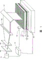
Fig. 1 is the skeleton view that manufacturing installation is shown;
Fig. 2 A to 2C is the sectional view that the manufacture method of light-emitting device is shown;
Fig. 3 A and 3B are the figure that the position relationship in the opening of mask and laser radiation zone is shown;
Fig. 4 A and 4B are the figure that the position relationship in the opening of mask and laser radiation zone is shown;
Fig. 5 is the figure that the position relationship in the opening of mask and laser radiation zone is shown;
Fig. 6 A to 6C is the sectional view that the manufacture method of light-emitting device is shown;
Fig. 7 A to 7C is vertical view and the sectional view of passive matrix light-emitting device;
Fig. 8 is the skeleton view of passive matrix light-emitting device;
Fig. 9 is the vertical view of passive matrix light-emitting device;
Figure 10 A and 10B are the figure that the structure of light-emitting device is shown;
Figure 11 A to 11E is the figure that the example of electrical equipment is shown;
Figure 12 is the figure that the example of electrical equipment is shown.
Embodiment
Below, embodiments of the present invention are described.
Fig. 1 is the skeleton view of an example of manufacturing installation of the present invention.The laser that is launched is exported from laser oscillation apparatus 103 (YAG laser aid, excimer laser device etc.).This laser through being used for shape of beam form rectangle the first optical system 104, be used for shaping the second optical system 105, be used for forming the 3rd optical system 106 of collimated beam, then its light path is reflected mirror 107 and is bent into the direction vertical with illuminated substrate 101.Then, optionally make laser beam shine light absorbing zone 114 through having the mask 110 of light transmission opening.
As the mask 110 with opening, use can be born the material of laser radiation.In addition, do not use near the mask of the taper of the point of opening, and use the inwall of its opening along the mask of the working direction of light beam.
In addition, the shape that shines the laser beam spot of the layer (light absorbing zone or γ-ray emission layer) that is provided at illuminated substrate is preferably rectangle or linear, and being in particular minor face is that 1mm to 5mm and long limit are the rectangles of 10mm to 50mm.In addition, in the situation that use the big area substrate, the long limit of laser beam spot is preferably 20cm to 100cm, to shorten the treatment time.In addition, also can provide a plurality of laser oscillation apparatus shown in Figure 1 and optical system to process at short notice the big area substrate.Particularly, also can from a plurality of laser oscillation apparatus respectively illuminating laser beam share a processing area substrate.
Note, Fig. 1 is an example, is configured in each optical system of light path of laser and the position relationship of electrooptic cell and has no particular limits.For example, be configured in the top of illuminated substrate 101 when laser oscillation apparatus 103, and when configuring in the mode that the laser from laser oscillation apparatus 103 emission becomes the direction vertical with the principal plane of illuminated substrate 101, also can not use speculum.In addition, as each optical system, use condensor, optical beam expander, homogenizer or polarizer to get final product, can also make up them.In addition, also can make up the line of rabbet joint as each optical system.
By on plane of illumination with the mode of the Quadratic Finite Element irradiation area of scanning laser beam suitably, the wide area on substrate is shone.For scanning relatively irradiation area and the substrate of mobile laser beam.At this, using in the horizontal direction, the mobile mobile unit (not shown) of the substrate Stage microscope 109 of substrate that keeps scans.
In addition, control the mobile unit of moving substrate Stage microscope 109 in the horizontal direction control device 116 preferred linkages.Moreover, control device 116 preferably also linkage ground control laser oscillation apparatus 103.And, the position registration mechanism interlock of control device 116 preferred imaging apparatus 108 with having the recognizing site mark.
Position registration mechanism is to mask 110, illuminated substrate 101, carried out position alignment by film forming substrate 100.In addition, also can configure mask 110 and illuminated substrate 101 with contacting with each other, have the interval therebetween but preferably make, in order to prevent the thermal conduction that mask 110 produces.
In addition, on a face of the irradiated illuminated substrate 101 of laser in advance in order stratification light absorbing zone 114 and material layer 115 are arranged.As light absorbing zone 114, preferably use thermotolerance metal such as tungsten, tantalum etc.
In addition, illuminated substrate 101 and by film forming substrate 100 with spacing distance d, 5mm is with the configuration of getting off at least.In addition, in the situation that provided the isolator that becomes partition wall by film forming substrate 100, also can make isolator and material layer 115 configure illuminated substrate 101 and by film forming substrate 100 with contacting with each other.
In the situation that use manufacturing installation shown in Figure 1 to carry out film forming, configure at least illuminated substrate 101 and by film forming substrate 100 vacuum-treat is indoor.In addition, also all structures shown in Figure 1 can be configured in vacuum-treat indoor.
In addition, manufacturing installation shown in Figure 1 towards the example of top what is called towards the film deposition system of upper type, still also can be adopted the film deposition system of mode down by the film forming face of film forming substrate 100.In addition, in the situation that are big area substrates by film forming substrate 100, also can adopt will be by the perpendicular film deposition system of erectting mode for the what is called vertical with horizontal plane of the principal plane of film forming substrate 100, to prevent making substrate center crooked because of the weight of substrate itself.
In addition, by also providing cooling by the cooling unit of film forming substrate 100, the flexible substrate such as plastic can be used as by film forming substrate 100.
In addition, can provide the manufacturing installation shown in a plurality of present embodiments to form the multichamber type manufacturing installation.Certainly, also can make up the film deposition system that adopts other films.In addition, also can pass through the manufacturing installation arranged in series shown in a plurality of present embodiments, and form the tandem type manufacturing installation.
Embodiment 2
At this, Fig. 2 A, Fig. 2 B and Fig. 2 C illustrate the situation after using manufacturing installation formation film shown in Figure 1 before.
As illuminated substrate 200, use the translucent glass substrate, form light absorbing zone 201 on this substrate, and form layer 202 (Fig. 2 A) that include organic compounds on light absorbing zone.
By adopting sputtering method etc. and using the target of tantalum, titanium, molybdenum or tungsten or the target of the alloy that is made of above-mentioned material forms light absorbing zone 201.At this, form the thick tungsten film of 100nm by sputtering method.Can for being thicker than 100nm, its absorbing laser bundle be generated heat by the thickness that makes light absorbing zone 201.Note, if light absorbing zone 201 heatings to the sublimation temperature that is included in the organic compound in the layer 202 that includes organic compounds, also can make the part of laser beam see through light absorbing zone 201.But, in the situation that the part of laser beam sees through, preferably adopt the organic compound that does not decompose because of the irradiation of laser beam.
In addition, form as the dissolving in solvent of coating liquid or the liquid that is dispersed with organic compound (or its precursor) layer 202 that includes organic compounds by coatings such as wet type operation such as spin-coating method, spraying method, dip coatings.Layer 202 as including organic compounds also can use the inorganic materials of molybdenum oxide etc. and the matrix material of organic materials.Organic compound preferably has solvability or dispersiveness to solvent.Be formed in the operation of back by the film thickness of the layer 211 that includes organic compounds on film forming substrate 206 and the adjusting that homogeneity depends on this coating liquid.Therefore, importantly: the organifying compound dissolves equably or is dispersed in coating liquid.In addition, in the situation that use spin-coating method, can regulate film thickness according to the degree of adhesion of coating liquid and the rotation number of substrate etc.
As solvent, use polar solvent or nonpolarity solvent.As polar solvent, can enumerate water, lower alcohol such as methyl alcohol, ethanol, n-propyl alcohol, i-propyl alcohol, n-butanols, sec-butanols etc., THF, acetonitrile, methylene dichloride, ethylene dichloride, methyl-phenoxide etc., can also mix the multiple of above-mentioned materials and use.In addition, as nonpolarity solvent, can enumerate hexane, benzene, toluene, chloroform, ethyl acetate, tetrahydrofuran (THF), chloromethyl etc., can also mix the multiple of above-mentioned materials and use.
As organic compound, suitably use according to the solvent that uses and be selected from luminophore as follows, get final product.for example, when obtaining red colour system when luminous, the luminous material that is presented on the peak value that has emmission spectrum in the scope of 600nm to 680nm is got final product as luminophore, for example, 4-dicyano methylene-2-sec.-propyl-6-[2-(1, 1, 7, 7-tetramethyl-julolidine-9-yl) vinyl]-(abbreviation: DCJTI) of 4H-pyrans, 4-dicyano methylene-2-methyl-6-[2-(1, 1, 7, 7-tetramethyl-julolidine-9-yl) vinyl]-(abbreviation: DCJT) of 4H-pyrans, 4-dicyano methylene-2-the tertiary butyl-6-[2-(1, 1, 7, 7-tetramethyl-julolidine-9-yl) vinyl]-(abbreviation: DCJTB) of 4H-pyrans, pyridine alcohol, 2, 5-dicyano-1, two [2-(10-methoxyl group-1 of 4-, 1, 7, 7-tetramethyl-julolidine-9-yl) vinyl] benzene etc.
In addition, when will to obtain green be luminous, the luminous material that is presented on the peak value that has emmission spectrum in the scope of 500nm to 550nm is got final product as luminophore, N for example, (the abbreviation: DMQd), the coumarin 6, (abbreviation: Alq3) etc. of tonka bean camphor 545T, three (oxine closes) aluminium of N '-dimethylquinacridone.
in addition, when obtaining blue series when luminous, the luminous material that is presented on the peak value that has emmission spectrum in the scope of 420nm to 500nm is got final product as luminophore, for example 9, (the abbreviation: t-BuDNA) of 10-two (2-naphthyl)-2-tert-butyl anthracene, 9,9 '-bismuth anthryl, 9, (the abbreviation: DPA) or 9 of 10-diphenylanthrancene, two (2-naphthyl) anthracene (abbreviations: DNA) of 10-, (the abbreviation: BGaq) of two (2-methyl-oxine)-4-phenylphenol oxygen base-galliums, perhaps two (2-methyl-oxine)-4-phenylphenol oxygen base-aluminium (abbreviations: BAlq) etc.
In addition, for the material for disperseing luminophore to use together with luminophore, have no particular limits, for example can use 9, (the abbreviation: the anthracene derivant, 4 such as t-BuDNA) of 10-two (2-naphthyl)-2-tert-butyl anthracene, 4 '-two (N-carbazyl) biphenyl (abbreviation: the carbazole derivative such as CBP), and can use (the abbreviation: Znpp2) or (abbreviation: the metal complexes etc. such as ZnBOX) of two [2-(2-hydroxyphenyl) benzoxazole] zinc of two [2-(2-hydroxyphenyl) pyridine] zinc.
And, be formed with light absorbing zone 201 and include on layer 202 the illuminated substrate surface of organic compounds relative position configuration by film forming substrate 206.In addition, in this manual, the first electrode refers to become the electrode of the male or female of luminous element.Luminous element has the structure that the layer that includes organic compounds that comprises on the first electrode, this first electrode and this include the second electrode on the layer of organic compounds, and the electrode that will first be formed on substrate on the formation order is called the first electrode.Isolator 208 covers the end of the first electrode 207.Material as the first electrode 207 preferably uses the large material of work content rate.For example, except the unitary film of indium tin oxides film, the indium tin oxides film that comprises silicon, indium zinc oxide film, titanium nitride film, chromium film, tungsten film, zinc film, platinum film etc., can also use titanium nitride film and with the lamination of aluminium as the film of main component; The three-decker of titanium nitride film, the film take aluminium as main component and titanium nitride film etc.
In addition, configure the mask 205 with opening on the position relative with another face of illuminated substrate 200.
And, with the laser beam irradiation of rectangle to mask 205 and will be through the laser beam flying of the opening of mask to the face of light absorbing zone 201.Light absorbing zone 201 heatings in the zone of illuminated laser beam, and utilize this heat energy to come the gasification of organifying compound.The organic compound that has gasified is attached on the first electrode 207.Owing to by the spacing distance d of film forming substrate and illuminated substrate being short range below 5mm, the layer 211 that includes organic compounds that therefore has with the area of the roughly the same size of the port area of mask is formed on by (Fig. 2 C) on film forming substrate 206.Note, form film under reduced atmosphere.Carry out vacuum exhaust so that its vacuum tightness is set as 5 * 10 by use vacuum exhaust unit in filming chamber
-3Below Torr (0.665Pa), be preferably set to 10
-4Pa to 10
-6Pa can obtain above-mentioned reduced atmosphere.
In addition, although Fig. 2 C illustrates with the example to the vertical mode irradiating laser of the principal plane of illuminated substrate, be not limited to this, the mode that also can tilt to the principal plane of illuminated substrate is shone.For example, change focal length by the thickness of controlling optical system and illuminated substrate, also the layer that includes organic compounds of the area of the size less than the port area of mask can be formed on by on the film forming substrate.
Then, form the second electrode by the electron beam evaporation plating method.As the second electrode, use aluminium, silver or its alloy.By above-mentioned operation, can form luminous element.
In addition, although Fig. 2 C illustrates layer 202 the figure that includes organic compounds of the position in the zone that is not overlapped in illuminated laser beam, be not limited to this.Be used as in the situation that will be dispersed with the polymkeric substance of organic compounds the layer that includes organic compounds, also optionally the organifying compound gasifies to make polymkeric substance to stay.
In addition, Fig. 2 C illustrates by film formation process once and carry out respectively the example of film forming on the first adjacent electrode 207, but in the situation that make the full color display unit, be respectively formed in mutually different zone by the luminescent layer that repeatedly film formation process is different with glow color.
Below, explanation can be carried out the manufacturing example of the light-emitting device of full color demonstration.At this, the example of the light-emitting device of the luminescent layer that uses three kinds of colors is shown.
Prepare the illuminated substrate shown in three Fig. 2 A.Form respectively the different layers that includes organic compounds on each illuminated substrate.Particularly, prepare to provide the first illuminated substrate of the material layer that red light emitting layer uses, the 3rd illuminated substrate that provides the second illuminated substrate of the material layer that green light emitting layer uses and provide the material layer that blue light-emitting layer uses.
In addition, prepare one provide the first electrode by the film forming substrate.Note, the isolator that becomes partition wall of the end that covers the first electrode is provided, produce each other short circuit to prevent the first adjacent electrode.The zone that becomes light-emitting zone is equivalent to the part of the first electrode, namely is not overlapped in isolator and the zone of exposing.
And, overlapping by film forming substrate and the first illuminated substrate.Moreover, overlapping mask 14 on the first illuminated substrate, and carry out position alignment to mask 14 with by the film forming substrate.Mask 14 provides the opening 16 that has with the roughly the same size of light-emitting zone.Carry out position alignment owing to need to and being provided at by the first electrode of film forming substrate this opening 16, therefore the position alignment mark preferably is provided on mask 14.In addition, preferably also provide the position alignment mark on by the film forming substrate.In addition, because the first illuminated substrate provides light absorbing zone, so preferably remove in advance near the light absorbing zone of mark of position alignment.In addition, because the first illuminated substrate provides the material layer that red light emitting layer is used, so preferably remove in advance the material layer that near the red light emitting layer of mark of position alignment is used.
And, so that its long side direction mode parallel with the minor face of the opening 16 of rectangle shone linear laser beam, come the enterprising line scanning of long side direction at the opening 16 of rectangle.By using the mask provide respectively with the opening 16 of the roughly the same size of Pixel Dimensions, can prevent from forming material layer between adjacent pixel.The mask that has this opening 16 by employing can provide contact part between adjacent pixel.In other words, in the luminous element of the second electrode on having the first electrode and this first electrode, the contact hole of the wiring that is used for being electrically connected to the second electrode that is provided at the first electrode top can be formed between the first adjacent electrode.Due to form when the shape with opening than two pixels of longitudinal arrangement amount to the long bar shaped of size the time, material layer can be formed on therebetween, therefore needs to remove the operation of this material layer.
In the zone through opening 16 and illuminated laser beam, the light absorbing zone heating, the organic compound that comprises in the material layer that red light emitting layer uses that contact with this light absorbing zone evaporates, and carries out film forming for the first time on being provided at by the first electrode of film forming substrate.After film forming finishes for the first time, the first illuminated substrate is moved to and the place that is separated by the film forming substrate.
Then, overlapping by film forming substrate and the second illuminated substrate.Then, use identical mask 14 to depart from film forming for the first time the time on the position of a pixel overlapping by film forming substrate and the second illuminated substrate.
And, so that its long side direction mode parallel with the minor face of the opening 16 of rectangle shone linear laser beam, come the enterprising line scanning of long side direction at the opening 16 of rectangle.
In the zone through opening 16 and illuminated laser beam, the light absorbing zone heating, the organic compound that is included in the material layer that green light emitting layer uses that contact with this light absorbing zone evaporates, and carries out film forming for the second time on being provided at by the first electrode of film forming substrate.After film forming finishes for the second time, moved to and the place that is separated by the film forming substrate by the film forming substrate second.
Then, overlapping by film forming substrate and the 3rd illuminated substrate.Then, use identical mask 14 to depart from film forming for the first time the time on the position of two pixels overlapping by film forming substrate and the 3rd illuminated substrate.
And so that its long side direction mode parallel with the minor face of the opening 16 of rectangle shone linear laser beam, film forming is for the third time carried out in scanning on the long side direction of the opening 16 of rectangle.The vertical view of Fig. 3 A is equivalent to be about to carry out this film forming situation before for the third time.In addition, not the first electrode of covering of insulated body 20 expose the zone be positioned at opening 16 overlapping position on.As the scanning direction 11, relatively move the irradiation area 10 of linear laser beam take the direction of the arrow shown in Fig. 3 A.Note, in Fig. 3 A, the first film 21 that has formed by film forming for the first time and the second film 22 that has formed by film forming for the second time are positioned at the below in zone shown in broken lines.
And, by after film forming forms tertiary membrane 23 for the third time, mask 14 and the 3rd illuminated substrate are moved to and the place that is separated by the film forming substrate.The vertical view of this moment is equivalent to Fig. 3 B.
Like this, have certain interval and also optionally form the first film 21, the second film 22, tertiary membrane 23.And, form the second electrode by the electron beam evaporation plating method and form luminous element on above-mentioned film.
By above-mentioned operation, can make the full color display unit.
Although at this example that is shaped as rectangle that shows the opening 16 of mask 14, the shape of opening also can adopt bar shaped shown in Figure 1, and is not limited to this.When adopting the opening of bar shaped, present between the light-emitting zone of identical glow color and also be formed with film, yet owing to being formed on isolator 20, therefore do not become light-emitting zone with the overlapping part of isolator 20.
In addition, the arrangement of pixel has no particular limits, and both can as shown in Figure 4B, a primitive shape be made as polygon, sexangle for example can configure again the indicating meter that the first film (R) 41, the second film (G) 42, tertiary membrane (B) 43 are realized full color.When polygonal pixel that will form shown in Fig. 4 B, use the mask with hexagonal opening 36 34 shown in Fig. 4 A, and form and get final product when relatively form film in the irradiation area 10 of mobile laser beam on scanning direction 11.
In addition, the film forming of carrying out for the luminescent layer that forms three kinds of colors is not limited to three times, also can carry out film forming more frequently.For example, use mask 54 shown in Figure 5 when carrying out film forming for the first time, and in the situation that the first illuminated substrate is remained on identical position, scanning laser beam carries out film forming for the second time by mask 54 is departed from three pixels.By so repeatedly carrying out film forming, complete the formation of the first film.And, form the second film (G), tertiary membrane (B) with the same manner.By adopting this film, can reduce the opening number of mask and make and have long distance between adjacent opening, thereby can improve the working accuracy of mask.In addition, in the opening shown in Fig. 3 A, simultaneously adjacent by a plurality of zones of the light absorbing zone of laser beam heats, but in the situation that adopt the configuration of opening shown in Figure 5, reduced by the quantity of the light absorbing zone of laser beam heats simultaneously, and can suppress heat conducting impact.In addition, the interval of the light-emitting zone of upward arranging is in the row direction narrowed down, and the interval of the light-emitting zone of arranging on column direction is narrowed down.
In addition, show the long side direction of linear laser beam and the example of the direction quadrature that uses described scanning element scanning here, but be not limited to this.In addition, the relation of the opening of mask and the scanning direction of laser beam also has no particular limits, and also can be for the opening of rectangle, with the scanning direction perpendicular or parallel with the diagonal lines of this opening.Reduced by the quantity of the light absorbing zone of laser beam heats simultaneously similarly in the case, and can suppress heat conducting impact.Because translucent glass is to be not easy to produce heat conducting substrate, so not when mask is heated, this thermal conduction is to the worry of light absorbing zone.But due to the sweep velocity and the affected worry of intensity that have because of laser beam, therefore suitably regulate.
In addition, present embodiment can freely make up with embodiment 1.
Embodiment 3
Embodiment 2 shows the example that uses light absorbing zone, but Fig. 6 is A, 6B and 6C illustrate the example of using the γ-ray emission layer that produces gas by irradiation light to replace light absorbing zone.
Prepare illuminated substrate 300.Use the quartz substrate of light transmission as illuminated substrate 300, and form γ-ray emission layer 301 on this substrate, form layer 302 (Fig. 6 A) that include organic compounds on this γ-ray emission layer 301.
As γ-ray emission layer 301, use more than 2 atom % and comprise the amorphous silicon film of hydrogen in the concentration range below 20 atom %, produce by irradiating ultraviolet light and decompose the resin combination etc. that produces triazo-compound and the overlapping nitride of gas and contain micro bubble.In the present embodiment, as γ-ray emission layer 301, use using plasma CVD method and comprise the amorphous silicon film of hydrogen with the concentration range of 8 atom %.
In addition, as the layer 302 that includes organic compounds, use the material identical with the layer 202 that includes organic compounds shown in embodiment 2 to get final product.Moreover the layer 302 as including organic compounds also can use the aggregate (molecule number is preferably below 10) that there is no sublimability and deliquescent organic compound.Layer 302 as including organic compounds can use low molecular organic materials, high molecular organic materials, have the organic materials of the middle molecule of the character between low molecule and polymer.In addition, as the layer 302 that includes organic compounds, can also use the matrix material of organic compound and mineral compound.The organic materials of middle molecule refers to that chain molecular length is below 5 μ m, is preferably the following organic compound of 50nm or there is no sublimability and the aggregate of deliquescent organic compound (molecule number is preferably below 10).
And, be formed with γ-ray emission layer 301 and include the relative position configuration of the face of layer 302 illuminated substrate of organic compounds by film forming substrate 306.In the present embodiment, be provided at by the isolator 308 of film forming substrate and be provided at the layer that includes organic compounds 302 o'clock of illuminated substrate in configuration, making their ground that contacts with each other overlapping.
Then, configure the mask 305 (Fig. 6 B) with opening on the position relative with another face of illuminated substrate 300.
And, with the laser beam irradiation of rectangle to mask 305 and will be through the laser beam flying of the opening of mask to the face of γ-ray emission layer 301.The γ-ray emission layer 301 in the zone of illuminated laser beam produces gas and partly peels off the layer that includes organic compounds.Because the layer 302 that includes organic compounds is films, therefore by γ-ray emission layer 301 being carried out ablation, the layer 302 that includes organic compounds is peeled off, and it is attached on the first electrode 307.In addition, because the γ-ray emission layer is removed, closely be connected on the first electrode 307 so include the layer 302 illuminated laser beam of organic compounds.Like this, the layer that includes organic compounds 311 is formed on by (Fig. 6 C) on film forming substrate 306.Note, under the inert gas atmosphere of having removed moisture, carry out film forming with normal atmosphere.In addition, also can carry out film forming under reduced atmosphere.
In addition, due to the layer 302 also illuminated laser beam being attached to the first electrode 307 after that includes organic compounds, therefore also can use by carrying out photopolymerisable monomer (organic compound) as the layer 302 that includes organic compounds and dissolve or be dispersed in liquid in solvent as coating liquid and adopt the wet type operation such as spin-coating method, spraying method, dip coating etc. apply the film that forms.As photopolymerisable monomer, suitably use according to the solvent that uses to be selected from following luminophore and to get final product.For example; with N-vinyl carbazole, 9; the vinyl (C=C-) of 9 '-dimethyl-2-ethene fluorenyl etc. and propionyl (C=C-COO-) and as the monomer with unsaturated double-bond base of allyl group (C=C-C-) etc. as luminophore, get final product.In addition, begin agent as photopolymerization, use 2-chlorine sulphur chitosan (chlorothiochitosan), benzophenone, ketone photopolymerization begin agent such as michaelis ketone etc., the acetophenones photopolymerization begins agent such as diethoxy acetophenone, 2-hydroxy-2-methyl-1-phenyl-propane-ketone etc. and benzil etc., get final product.
In addition, if need, also can carry out heat treated to the layer 311 that includes organic compounds.In the present embodiment, owing to using amorphous silicon film, therefore there is the powder of silicon to be attached to the lip-deep worry of the layer 311 that includes organic compounds.But can clean layer 311 the surface that includes organic compounds in this case.In addition, in the situation that replace comprising the amorphous silicon film of hydrogen as the γ-ray emission layer 301 overlapping nitride of use, because 301 gasification of γ-ray emission layer do not need to carry out clean.
In addition, present embodiment can freely make up with embodiment 1 or embodiment 2.
For the present invention who is consisted of by said structure, be described in detail with the embodiment shown in following.
At this, make the example of passive matrix light-emitting device with reference to Fig. 7 A to 7C, Fig. 8 and Fig. 9 explanation on glass substrate.
In passive matrix (simple matrix type) light-emitting device, be listed as a plurality of anodes of bar shaped (band shape) and be listed as a plurality of negative electrodes of bar shaped mutually orthogonal, and have the structure that luminescent layer or fluorescent layer are sandwiched in its cross part.Therefore, be equivalent to be selected the pixel of intersection point of the anode of (being applied in voltage) and selecteed negative electrode luminous.
Fig. 7 A is the vertical view of the pixel portions before sealing.The sectional view that blocks with dotted line A-A ' in Fig. 7 A is Fig. 7 B, and is Fig. 7 C with the sectional view that chain line B-B ' blocks.
In addition, Fig. 8 illustrates partition wall 1522 skeleton view afterwards of the parallel a plurality of anti-tapers of firm formation.Note, the part identical with Fig. 7 A to 7C adopts identical Reference numeral.
The height setting of the partition wall 1522 of anti-taper is the film thickness greater than the stack membrane that comprises luminescent layer and conducting film.When stratification on the first substrate with structure shown in Figure 8 comprises the stack membrane of luminescent layer and conducting film, as shown in Fig. 7 A to 7C, be separated into a plurality of zones of electricity isolation, and form stack membrane 1515R, 1515G, 1515B and the second electrode 1516 that comprises luminescent layer.The second electrode 1516 is the strip electrodes parallel to each other that extend to the direction of intersecting with the first electrode 1513.Note, also form stack membrane and the conducting film that comprises luminescent layer on the partition wall 1522 of anti-taper, but they are what to separate with the stack membrane 1515R, the 1515G that comprise luminescent layer, 1515B and the second electrode 1516.
At this, illustrate and optionally form stack membrane 1515R, 1515G, the 1515B that comprises luminescent layer, and form the example that can obtain three kinds (R, G, B) the luminous light-emitting device that can carry out the full color demonstration.Stack membrane 1515R, the 1515G, the 1515B that comprise luminescent layer are formed by difference bar paten parallel to each other.
In the present embodiment, use manufacturing installation shown in Figure 1 to form the stack membrane that comprises luminescent layer.Preparation be formed with the luminescent layer that can obtain emitting red light the first illuminated substrate, be formed with the luminescent layer that can obtain green emitting the second illuminated substrate, be formed with the 3rd illuminated substrate of the luminescent layer that can obtain blue-light-emitting.Then, also being moved in manufacturing installation shown in Figure 1 by the film forming substrate of the first electrode 1513 will be provided.And, will have identical with one side of substrate or than the illuminated substrate of laser beam irradiation to the first of its long irradiated area to add heat ray absorbing layer, carry out film forming.Then, suitably also optionally carrying out film forming on the second illuminated substrate, on the 3rd illuminated substrate.Due to by using manufacturing installation shown in Figure 1, can optionally carry out film forming, therefore also can not use the partition wall 1522 of anti-taper.
In addition, the stack membrane that both can form the luminescent layer that comprises the light of launching same color on whole surface provides monochromatic luminous element, can make again and can carry out the light-emitting device that the monochromatic light-emitting device that shows maybe can carry out the partial color demonstration.In addition, as obtaining white luminous light-emitting device, adopt by being combined into color filter and can carry out the light-emitting device that full color shows.
In addition, if necessary, seal with sealing material such as sealed can and glass substrate of being used for sealing etc.At this, use glass substrate as the second substrate, use the tackiness agent of sealing agent etc. fit the first substrate and the second substrate, thus sealing by the tackiness agent of sealing agent etc. around the space.Fill weighting agent, and dry rare gas element in sealed space.In addition, also can enclose drying material etc. between the first substrate and sealing agent, to improve the reliability of light-emitting device.Drying material is removed micro-moisture, thereby realizes dry fully.In addition, as drying material, can use by chemisorption to absorb the material of moisture such as the alkaline-earth metal of calcium oxide, barium oxide etc.Note, as other drying materials, also can use material such as zeolite and silica gel etc. by the physical adsorption adsorption moisture.
But, providing contact and the sealing material of covering luminous element, and fully with the exhausted situation of outer air bound under, drying material need not be provided.
Then, Fig. 9 illustrates the vertical view of the light emitting module that FPC etc. is installed.
As shown in Figure 9, in the pixel portions that composing images shows, scanning line-group and data line-group intersect mutually orthogonally.
Note, sweep trace 1603 is electrically connected to connecting wiring 1608 at the cloth thread end, and connecting wiring 1608 is connected to FPC1609b by input terminal 1607.And data line 1602 is connected to FPC1609a by input terminal 1606.
If necessary, can suitably provide blooming such as polaroid, circular polarizing disk (comprising ellipsoidal polarizing plate), polarizer (λ/4 plates, λ/2 plates) and color filter etc. on emitting surface.In addition, also can provide anti-reflective film on polaroid or circular polarizing disk.For example, can carry out anti-dazzle and process, this processing is to utilize the concavo-convex of surface come diffused reflection light and reduce dazzle.
By above-mentioned operation, can make the passive matrix light-emitting device with flexibility.If the manufacturing installation of the application of the invention and can not use the partition wall of anti-taper just can make significantly component structure simplify, and can reduce the needed time of manufacturing process.
In addition, although Fig. 9 shows the example that driving circuit is not provided on substrate, the IC chip with driving circuit can be installed also.
In the situation that the IC chip is installed, installs respectively by the COG mode in periphery (outside) zone of pixel portions and be formed with data line one side IC, the sweep trace one side IC that each signal is transferred to the driving circuit of pixel portions.Field engineering as beyond the COG mode also can adopt TCP, Bonding mode to install.TCP is installed to the TAB adhesive tape with IC, by the wiring that the TAB adhesive tape is connected on element formation substrate, IC is installed.Data line one side IC and sweep trace one side IC use silicon substrate and the IC that forms, can be also by using TFT to form the IC that driving circuit forms on glass substrate, quartz substrate or plastic.In addition, although the example that provides an IC for a side here is illustrated, also can provide in a side to be split up into a plurality of IC.
In addition, the present embodiment can freely make up with any one of embodiment 1 to 3.
Embodiment 2
In the present embodiment, the active array type light-emitting device for using manufacturing installation shown in Figure 1 to form describes with reference to Figure 10.Note, Figure 10 A is the vertical view that light-emitting device is shown, and Figure 10 B is the sectional view that the A-A ' line along Figure 10 A blocks.Reference numeral 1701 shown in dotted line is that driving circuit section (source electrode one side drive circuit), Reference numeral 1702 are that pixel portions, Reference numeral 1703 are driving circuit sections (grid one side drive circuit).In addition, Reference numeral 1704 is that seal substrate, Reference numeral 1705 are sealing agents, by sealing agent 1705 around the Reference numeral 1707 of inboard be the space.
Note, Reference numeral 1708 is wirings of transmitting the signal that is input to source electrode one side drive circuit 1701 and grid one side drive circuit 1703, from FPC (flexible print circuit) 1709 receiving video signals of external input terminals, clocksignal, initial pulse, reset signal etc.Note, although at this, FPC is shown, this FPC also can be equipped with printed wiring substrate (PWB).As the light-emitting device of this specification sheets, except the light-emitting device main body, also be included in the light-emitting device that FPC or PWB are installed on the light-emitting device main body.
Then, illustrate with Figure 10 B for cross section structure.Be formed with driving circuit section and pixel portions on component substrate 1710, still, source electrode one side drive circuit 1710 and pixel portions 1702 in the section of driving circuit this illustrate.
Note, be formed with combination n channel-type TFT1723 and p channel-type TFT1724 and the cmos circuit that forms in source electrode one side drive circuit 1701.In addition, the circuit of formation driving circuit also can be formed by known cmos circuit, PMOS circuit or nmos circuit.In addition, although that the present embodiment illustrates the driving mechanism that is formed with driving circuit on same substrate is one-piece type,, also can externally form driving circuit not on substrate, and not necessarily adopt driving mechanism one-piece type.
In addition, pixel portions 1702 is made of a plurality of pixels that comprise switching TFT 1711, current control TFT1712 and be electrically connected to the anode 1713 of its drain electrode.Note, be formed with isolator 1714 in the mode of the end that covers anode 1713.At this, isolator 1714 is by using positive type light sensitive acrylic resin film to form.
In addition, isolator 1714 forms thereon the end or the bottom has the curved surface of curvature in order to have good spreadability.For example, in the situation that the positive type light sensitive acrylic resin film is used for isolator 1714, be preferably formed the curved surface that the upper end of only having isolator 1714 has radius-of-curvature (0.2 μ m to 3 μ m).In addition, as isolator 1714, can use the minus material that becomes and be insoluble to etching reagent because of photosensitive light, perhaps use because light becomes and dissolve in the positive shaped material of etching reagent, and can use organic compound and mineral compound such as silicon oxide, silicon oxynitride etc.
Be formed with luminous element 1715 and negative electrode 1716 on anode 1713.At this, the material as being used for anode 1713 preferably uses the large material of work function.For example, can use following material: unitary film such as indium tin oxides film, the indium tin oxides film that comprises silicon, indium zinc oxide film, titanium nitride film, chromium film, tungsten film, Zn film, Pt film etc.; The lamination of titanium nitride film and the film take aluminium as main component; The three-decker of titanium nitride film, the film take aluminium as main component and titanium nitride film etc.In addition, when anode 1713 is indium tin oxides film, and when the wiring of the current control TFT1712 that is connected with anode 1713 is the lamination of the lamination of titanium nitride film and the film take aluminium as main component or titanium nitride film, the film take aluminium as main component and titanium nitride film, resistance as wiring is low, and obtain to contact with the good ohmic of indium tin oxides film, and can make anode 1713 play the effect of anode.In addition, anode 1713 also can be formed by the material identical with the first anode in luminous element 1715.Perhaps, anode 1713 can be stacked contiguously with the first anode of luminous element 1715.
In addition, luminous element 1715 has stacked anode 1713, include the layer 1700 of organic compounds and the structure of negative electrode 1716, specifically, and suitably stacked hole injection layer, hole transmission layer, luminescent layer, electronics input layer or electron injecting layer.Form by any film deposition system with embodiment 1 or embodiment 3, get final product.
Moreover, as the material that is used for negative electrode 1716, use the little material (alloy of Al, Ag, Li, Ca or above-mentioned materials such as MgAg, MgIn, AlLi, Calcium Fluoride (Fluorspan) or CaCl2) of work function to get final product, but be not limited to these materials.By selecting suitable electron injection material, can use various conducting films.Note, in the situation that make the luminous negative electrode 1716 that sees through of self-emission device 1715, can use following method: as negative electrode 1716, the lamination of the metallic film of use thin film thickness, the Indium sesquioxide stannic oxide alloy of nesa coating, Indium sesquioxide oxide zinc-oxide alloy, zinc oxide etc.In addition, negative electrode 1716 also can be formed by the material identical with the second negative electrode in luminous element 1715.Perhaps, negative electrode 1716 also can be stacked in the mode that contacts with the second negative electrode of luminous element 1715.
Moreover, by using sealing agent 1705 gluing, sealing substrates 1704 and component substrate 1710, become by component substrate 1710, seal substrate 1704 and sealing agent 1705 around space 1707 in possess the structure that luminous element 1715 is arranged.Note, in space 1707, except the situation that is filled with rare gas element (nitrogen or argon etc.), also comprise the situation of being filled by sealing agent 1705.
Note, preferably use redix as sealing agent 1705.In addition, these materials preferably do not see through the material of moisture and oxygen as far as possible.In addition, as the material that is used for seal substrate 1704, except glass substrate and quartz substrate, can also use the plastic that is consisted of by FRP (glass filament reinforced plastics), PVF (fluorinated ethylene propylene), polyester or propylene etc.
By above-mentioned steps, can obtain to have with manufacturing installation of the present invention the light-emitting device of luminous element.Although the active array type light-emitting device easily uprises the needed manufacturing cost of each light-emitting device because making TFT, but not with the manufacturing installation of the present invention shown in Figure 1 of the manufacturing installation of film thickness watch-dog by shortening significantly the film forming treatment time of each substrate with the big area substrate, thereby can realize the significantly cost degradation of each light-emitting device.In addition, can realize the cost degradation of manufacturing cost because of the utilising efficiency that can improve material.
Note, the light-emitting device shown in the present embodiment can freely make up the film shown in the film deposition system shown in embodiment 1 or embodiment 2 or embodiment 3 and implement.Moreover the light-emitting device shown in the present embodiment also can use the chroma conversion film of color filter etc. as required.
In addition, as the active coating of the TFT that is configured in pixel portions 1702, can suitably use amorphous semiconductor film, comprise crystalline texture semiconductor film, comprise the compound semiconductor film of non-crystal structure etc.Moreover, active coating as TFT, can use hemihedral crystal semiconductor film (also referred to as microcrystalline semiconductor film (microcrystal semiconductor film)), this hemihedral crystal semiconductor film is to have intermediate structure noncrystalline and crystalline texture (comprising monocrystalline, polycrystalline), and having the semi-conductor of elicit illness state stable aspect free energy, it comprises the crystal region with short range order and lattice distortion.In the zone of at least a portion in the hemihedral crystal semiconductor film, comprise the crystal grain of 0.5nm to 20nm, and Raman spectrum moves to lower than 520cm
-1Wave number one side.In addition, observe (111), the diffraction peak of (220) that the lattice by silicon causes in the X-ray diffraction of hemihedral crystal semiconductor film.In addition, the hemihedral crystal semiconductor film contains at least 1 atom % or more hydrogen or halogen, in order to make the dangling bonds neutralization.As the manufacture method of hemihedral crystal semiconductor film, to material gas SiH for example
4, Si
2H
6, SiH
2Cl
2, SiHCl
3, SiCl
4, SiF
4Decompose (plasma CVD) and form Deng carrying out glow discharge.One or more rare gas elements that use H2 or H2 and be selected from He, Ar, Kr, Ne dilute these materials.Thinning ratio is in the scope of 2 times to 1000 times.Pressure is in the scope of 0.1Pa to 133Pa, and supply frequency is 1MHz to 120MHz, preferably 13MHz to 60MHz.Substrate heating temperature is to get final product below 300 ℃, preferably 100 ℃ to 250 ℃.As the impurity element in film, the impurity of the Atmospheric components of oxygen, nitrogen, carbon etc. preferably 1 * 10
20cm
-1Below, especially, oxygen concn is 5 * 10
19cm
3Below, preferably 1 * 10
19cm
3Below.Note, the electrical effect mobility [mu] that the hemihedral crystal semiconductor film is used as the TFT of active coating is 1cm
2/ Vsec to 10cm
2/ Vsec.
Embodiment 3
In the present embodiment, having for use the various electrical equipments that the light-emitting device of the luminous element that forms according to manufacturing installation of the present invention completes with reference to Figure 11 A to 11E describes.
can enumerate TV with the electrical equipment that manufacturing installation of the present invention forms, filming apparatus such as pick up camera and digital camera etc., goggle-type indicating meter (helmet-mounted display), navigationsystem, audio reproducing apparatus (automobile audio, audible component etc.), notebook personal computer, game machine, portable data assistance (portable computer, mobile telephone, portable game machine, e-book etc.), possesses the image-reproducing means of recording medium (specifically, the recording medium of reproduction digital video disk (DVD) etc., and can show the display unit of its image), set lights etc.Figure 11 A to 11E illustrates the object lesson of above-mentioned electrical equipment.
Figure 11 A is display unit, and it comprises framework 8001, brace table 8002, display part 8003, speaker portion 8004, video input terminal 8005 etc.Make display unit by its display part 8003 will be used for the light-emitting device that the present invention forms.Note, display unit comprises all information display unit such as the display unit that is used for Personal Computer, be used for receiving the display unit of TV broadcasting, be used for showing the display unit of advertisement etc.By adopting manufacturing installation of the present invention, can reduce significantly manufacturing cost, thereby cheap display unit can be provided.
Figure 11 B is notebook personal computer, and it comprises main body 8101, framework 8102, display part 8103, keyboard 8104, external connection port 8105, position determining equipment 8106 etc.This notebook personal computer is to be used for its display part 8103 by the light-emitting device that will have the luminous element that forms with manufacturing installation of the present invention to make.By means of manufacturing installation of the present invention, can reduce significantly manufacturing cost, thereby cheap notebook personal computer can be provided.
Figure 11 C is pick up camera, and it comprises main body 8201, display part 8202, framework 8203, external connection port 8204, telepilot acceptance division 8205, image acceptance division 8206, battery 8207, audio frequency input part 8208, operated key 8209, view finder 8210 etc.This pick up camera is to be used for its display part 8202 by the light-emitting device that will have the luminous element that forms with manufacturing installation of the present invention to make.By means of manufacturing installation of the present invention, can reduce significantly manufacturing cost, thereby cheap pick up camera can be provided.
Figure 11 D is desk-top set lights, and it comprises Lighting Division 8301, lampshade 8302, variable arm (adjustable arm) 8303, pillar 8304, estrade 8305, power supply 8306.This desk-top set lights is to make by being used for its Lighting Division 8301 with the light-emitting device that manufacturing installation of the present invention forms.Note, set lights also comprises the set lights that is fixed on top ceiling or wall-hanging set lights etc.By means of manufacturing installation of the present invention, can reduce significantly manufacturing cost, thereby cheap desk-top set lights can be provided.
Figure 11 E is mobile telephone, and it comprises main body 8401, framework 8402, display part 8403, audio frequency input part 8404, audio output part 8405, operated key 8406, external connection port 8407, antenna 8408 etc.This mobile telephone is to be used for its display part 8403 by the light-emitting device that will have the luminous element that forms with manufacturing installation of the present invention to make.By means of manufacturing installation of the present invention, can reduce significantly manufacturing cost, thereby cheap mobile telephone can be provided.
In addition, the example application of the mobile object with the light-emitting device that uses the luminous element that manufacturing installation of the present invention forms is installed for its means of illumination or display panel, describes with reference to Figure 12.Mobile object in the present embodiment comprises train, motor vehicle, aircraft etc., for example, can enumerate various mobile objects such as motorcycle, automatic brougham (comprising automobile, motorbus etc.), train (comprising single track, passenger train etc.) and ship etc.
The example that comprises the display panel of the light-emitting device with the luminous element that forms with manufacturing installation of the present invention for its display part, in Figure 12, the mobile object that display unit is one-piece type illustrates as an example.Figure 12 illustrates the example of display panel 9501 as the example of the one-piece type mobile object of display unit, and this display panel 9501 is arranged on motor vehicle 9502 integratedly.The display panel 9501 that display part shown in Figure 12 has is arranged on motor vehicle integratedly, thereby can show as required the information of work or or the outside input inner from car body of car body, and has the function of auto navigation to its point of destination.In addition, also can be with display panel 9501 as the illumination in car.
Note, application with light-emitting device of the luminous element that uses manufacturing installation formation of the present invention is not limited to the application of the previous section of car body shown in Figure 12, and can be applied to all parts such as top ceiling, glass port, door by changing its shape, and play the function of means of illumination or display unit.
By above-mentioned steps, can obtain to use electrical equipment, the set lights of the luminous element that forms according to manufacturing installation of the present invention.Range of application with the light-emitting device that uses the luminous element that manufacturing installation of the present invention forms is very extensive, and this light-emitting device can be applied to the electrical equipment of all areas.
Note, the light-emitting device shown in the present embodiment can freely make up the film shown in the film deposition system shown in embodiment 1 or embodiment 3 or embodiment 2 and implement.Any one that in addition, can freely make up embodiment 1 to 3 implemented.
The Japanese patent application numbering 2007-147413 that this specification sheets was accepted at Japan Office according on June 1st, 2007 makes, and described application content comprises in this manual.
Claims (10)
1. the manufacturing installation of a light-emitting device comprises:
The light source cell of Emission Lasers;
Described laser is formed the optical system of rectangle or linear laser beam;
Described rectangle or linear laser beam are optionally carried out shading, perhaps optionally reflect the light control unit of described rectangle or linear laser beam;
Will be through the laser beam flying of described light control unit the scanning element to the light absorbing zone that is provided at illuminated substrate; And
To described light control unit, described illuminated substrate, and carried out the aligned units of position alignment by the film forming substrate,
Wherein, laser beam through described light control unit heats described light absorbing zone, described light absorbing zone heats the first material layer that is provided at described illuminated substrate, so that at least a portion of described the first material layer gasification, and describedly form the second material layer on by the film forming substrate what relatively configure with described illuminated substrate.
2. the manufacturing installation of light-emitting device according to claim 1, it also comprises the control device of controlling described light source cell, described light control unit and described scanning element.
3. the manufacturing installation of light-emitting device according to claim 1, the long side direction of wherein said rectangle or linear laser beam and the scanning direction of described scanning element are orthogonal.
4. the manufacturing installation of light-emitting device according to claim 1, wherein said illuminated substrate is light-transmissive substrates.
5. the manufacturing installation of light-emitting device according to claim 1, wherein said light control unit be selected from photomask, the line of rabbet joint, and metal mask among.
6. the manufacturing installation of a light-emitting device comprises:
The light source cell of Emission Lasers;
Described laser is formed the optical system of rectangle or linear laser beam;
Described rectangle or linear laser beam are optionally carried out shading, perhaps optionally reflect the light control unit of described rectangle or linear laser beam;
Will be through the laser beam flying of described light control unit the scanning element to the γ-ray emission layer that is provided at illuminated substrate; And
To described light control unit, described illuminated substrate, and carried out the aligned units of position alignment by the film forming substrate, stacked γ-ray emission layer and the first material layer stated to some extent of this illuminated substrate,
Wherein, the laser beam of the described light control unit of process heats to make described γ-ray emission layer gasification to the described γ-ray emission layer that is provided at described illuminated substrate,
And, be configured to relative with described illuminated substrate describedly to form the second material layer on by the film forming substrate.
7. the manufacturing installation of light-emitting device according to claim 6, it also comprises the control device of controlling described light source cell, described light control unit and described scanning element.
8. the manufacturing installation of light-emitting device according to claim 6, the long side direction of wherein said rectangular laser bundle or linear laser bundle and the scanning direction of described scanning element are orthogonal.
9. the manufacturing installation of light-emitting device according to claim 6, wherein said illuminated substrate is light-transmissive substrates.
10. the manufacturing installation of light-emitting device according to claim 6, wherein said light control unit be selected from photomask, the line of rabbet joint, and metal mask among.
Applications Claiming Priority (3)
| Application Number | Priority Date | Filing Date | Title |
|---|---|---|---|
| JP2007147413 | 2007-06-01 | ||
| JP2007-147413 | 2007-06-01 | ||
| JP2007147413 | 2007-06-01 |
Publications (2)
| Publication Number | Publication Date |
|---|---|
| CN101314841A CN101314841A (en) | 2008-12-03 |
| CN101314841B true CN101314841B (en) | 2013-06-12 |
Family
ID=40088662
Family Applications (1)
| Application Number | Title | Priority Date | Filing Date |
|---|---|---|---|
| CN2008100999941A Expired - Fee Related CN101314841B (en) | 2007-06-01 | 2008-05-29 | Manufacturing apparatus and manufacturing method of light-emitting device |
Country Status (4)
| Country | Link |
|---|---|
| US (2) | US8232038B2 (en) |
| JP (3) | JP2009009935A (en) |
| KR (1) | KR101563237B1 (en) |
| CN (1) | CN101314841B (en) |
Families Citing this family (45)
| Publication number | Priority date | Publication date | Assignee | Title |
|---|---|---|---|---|
| US8080811B2 (en) | 2007-12-28 | 2011-12-20 | Semiconductor Energy Laboratory Co., Ltd. | Method for manufacturing evaporation donor substrate and light-emitting device |
| WO2009099002A1 (en) * | 2008-02-04 | 2009-08-13 | Semiconductor Energy Laboratory Co., Ltd. | Deposition method and method for manufacturing light-emitting device |
| JP2009231277A (en) * | 2008-02-29 | 2009-10-08 | Semiconductor Energy Lab Co Ltd | Manufacturing apparatus |
| JP5416987B2 (en) | 2008-02-29 | 2014-02-12 | 株式会社半導体エネルギー研究所 | Film forming method and light emitting device manufacturing method |
| WO2009107548A1 (en) * | 2008-02-29 | 2009-09-03 | Semiconductor Energy Laboratory Co., Ltd. | Deposition method and manufacturing method of light-emitting device |
| JP5238544B2 (en) * | 2008-03-07 | 2013-07-17 | 株式会社半導体エネルギー研究所 | Film forming method and light emitting device manufacturing method |
| JP5079722B2 (en) | 2008-03-07 | 2012-11-21 | 株式会社半導体エネルギー研究所 | Method for manufacturing light emitting device |
| US8182863B2 (en) | 2008-03-17 | 2012-05-22 | Semiconductor Energy Laboratory Co., Ltd. | Deposition method and manufacturing method of light-emitting device |
| US7993945B2 (en) * | 2008-04-11 | 2011-08-09 | Semiconductor Energy Laboratory Co., Ltd. | Method for manufacturing light-emitting device |
| US7932112B2 (en) * | 2008-04-14 | 2011-04-26 | Semiconductor Energy Laboratory Co., Ltd. | Method for manufacturing light-emitting device |
| JP5195451B2 (en) | 2008-04-15 | 2013-05-08 | 株式会社デンソー | FUEL INJECTION DEVICE AND PRESSURE ACCUMULATION FUEL INJECTION SYSTEM USED FOR THE SAME |
| US8409672B2 (en) * | 2008-04-24 | 2013-04-02 | Semiconductor Energy Laboratory Co., Ltd. | Method of manufacturing evaporation donor substrate and method of manufacturing light-emitting device |
| JP5159689B2 (en) * | 2008-04-25 | 2013-03-06 | 株式会社半導体エネルギー研究所 | Method for manufacturing light emitting device |
| KR101629637B1 (en) * | 2008-05-29 | 2016-06-13 | 가부시키가이샤 한도오따이 에네루기 켄큐쇼 | Deposition method and method of manufacturing light-emitting device |
| US7919340B2 (en) * | 2008-06-04 | 2011-04-05 | Semiconductor Energy Laboratory Co., Ltd. | Method for manufacturing light-emitting device |
| US8574709B2 (en) * | 2008-07-21 | 2013-11-05 | Semiconductor Energy Laboratory Co., Ltd. | Deposition donor substrate and method for manufacturing light-emitting device |
| JP5469950B2 (en) * | 2008-08-08 | 2014-04-16 | 株式会社半導体エネルギー研究所 | Method for manufacturing light emitting device |
| US8486736B2 (en) * | 2008-10-20 | 2013-07-16 | Semiconductor Energy Laboratory Co., Ltd. | Method for manufacturing light-emitting device |
| JP5291607B2 (en) * | 2008-12-15 | 2013-09-18 | 株式会社半導体エネルギー研究所 | Method for manufacturing light emitting device |
| KR101023133B1 (en) * | 2009-03-19 | 2011-03-18 | 삼성모바일디스플레이주식회사 | Organic light emitting diode display |
| JP5323784B2 (en) * | 2009-09-15 | 2013-10-23 | フオン・アルデンネ・アンラーゲンテヒニク・ゲゼルシヤフト・ミト・ベシユレンクテル・ハフツング | Method and apparatus for producing microstructures |
| JP2012124478A (en) * | 2010-11-19 | 2012-06-28 | Semiconductor Energy Lab Co Ltd | Illuminating device |
| WO2012133203A1 (en) * | 2011-03-30 | 2012-10-04 | シャープ株式会社 | Method for forming vapor deposition film pattern, and method for manufacturing organic electroluminescent display device |
| KR101328979B1 (en) | 2011-06-30 | 2013-11-13 | 삼성디스플레이 주식회사 | Organic light emitting display device |
| KR101813548B1 (en) * | 2011-06-30 | 2018-01-02 | 삼성디스플레이 주식회사 | Laser induced thermal imaging apparatus and method for manufacturing organic light emitting display device using the same |
| KR101787450B1 (en) * | 2011-08-09 | 2017-10-19 | 삼성디스플레이 주식회사 | Display apparatus |
| JP2013073822A (en) * | 2011-09-28 | 2013-04-22 | Ulvac Japan Ltd | Transfer deposition apparatus |
| EP2591875B1 (en) * | 2011-11-09 | 2017-01-25 | Leister Technologies AG | Laser with beam transformation lens |
| KR101959975B1 (en) * | 2012-07-10 | 2019-07-16 | 삼성디스플레이 주식회사 | Apparatus for organic layer deposition, method for manufacturing of organic light emitting display apparatus using the same, and organic light emitting display apparatus manufactured by the method |
| EP2731126A1 (en) | 2012-11-09 | 2014-05-14 | Nederlandse Organisatie voor toegepast -natuurwetenschappelijk onderzoek TNO | Method for bonding bare chip dies |
| WO2015083029A1 (en) | 2013-12-02 | 2015-06-11 | Semiconductor Energy Laboratory Co., Ltd. | Display device and method for manufacturing the same |
| CN104752469B (en) * | 2013-12-31 | 2018-08-03 | 昆山国显光电有限公司 | A kind of dot structure and the organic light emitting display using the dot structure |
| FR3025936B1 (en) * | 2014-09-11 | 2016-12-02 | Saint Gobain | METHOD FOR RECLAIMING FLASH LAMPS |
| CN105679967B (en) * | 2014-11-18 | 2018-06-26 | 昆山国显光电有限公司 | Mask plate, the method for preparing organic light-emitting display device |
| CN104795425A (en) * | 2015-03-30 | 2015-07-22 | 京东方科技集团股份有限公司 | Organic light emitting diode touch display screen and manufacturing method thereof |
| KR102388724B1 (en) * | 2015-08-21 | 2022-04-21 | 삼성디스플레이 주식회사 | Method of manufacturing mask for deposition |
| KR102404575B1 (en) | 2015-10-12 | 2022-06-03 | 삼성디스플레이 주식회사 | Deposition apparatus and manufacturing method of organic light emittion dioed display using the same |
| JP7020896B2 (en) * | 2017-12-14 | 2022-02-16 | 株式会社キーエンス | Laser processing equipment |
| US10138539B1 (en) * | 2018-04-03 | 2018-11-27 | Shiping Cheng | Method of managing coating uniformity with an optical thickness monitoring system |
| US11094530B2 (en) | 2019-05-14 | 2021-08-17 | Applied Materials, Inc. | In-situ curing of color conversion layer |
| US11239213B2 (en) * | 2019-05-17 | 2022-02-01 | Applied Materials, Inc. | In-situ curing of color conversion layer in recess |
| CN116034117A (en) | 2020-07-24 | 2023-04-28 | 应用材料公司 | Quantum dot formulations with thiol-based crosslinkers for UV-LED curing |
| CN115295561A (en) * | 2020-08-24 | 2022-11-04 | 武汉天马微电子有限公司 | Display panel, display device and manufacturing method |
| US11646397B2 (en) | 2020-08-28 | 2023-05-09 | Applied Materials, Inc. | Chelating agents for quantum dot precursor materials in color conversion layers for micro-LEDs |
| CN113770546A (en) * | 2021-10-11 | 2021-12-10 | 上海莘芝光电科技有限公司东莞分公司 | Process for manufacturing three-dimensional circuit by laser etching and carbonizing plastic surface |
Citations (3)
| Publication number | Priority date | Publication date | Assignee | Title |
|---|---|---|---|---|
| US6719916B2 (en) * | 2001-04-18 | 2004-04-13 | National Research Council Of Canada | Multilayer microstructures and laser based method for precision and reduced damage patterning of such structures |
| CN1540720A (en) * | 2003-04-21 | 2004-10-27 | ��ʽ����뵼����Դ�о��� | Beam radiating device, its radiating method and mfg. method of semiconductor device |
| CN1550568A (en) * | 2003-04-25 | 2004-12-01 | ��ʽ����뵼����Դ�о��� | Manufacturing device and light emitting device |
Family Cites Families (57)
| Publication number | Priority date | Publication date | Assignee | Title |
|---|---|---|---|---|
| EP0474494B1 (en) * | 1990-09-07 | 1997-12-29 | Dai Nippon Printing Co., Ltd. | Thermal transfer image receiving sheet and production process therefor |
| JPH0911646A (en) * | 1995-06-30 | 1997-01-14 | Fuji Photo Film Co Ltd | Thermal transfer sheet |
| EP0858110B1 (en) * | 1996-08-27 | 2006-12-13 | Seiko Epson Corporation | Separating method, method for transferring thin film device, and liquid crystal display device manufactured by using the transferring method |
| JP3801730B2 (en) * | 1997-05-09 | 2006-07-26 | 株式会社半導体エネルギー研究所 | Plasma CVD apparatus and thin film forming method using the same |
| US5937272A (en) * | 1997-06-06 | 1999-08-10 | Eastman Kodak Company | Patterned organic layers in a full-color organic electroluminescent display array on a thin film transistor array substrate |
| JPH1126733A (en) * | 1997-07-03 | 1999-01-29 | Seiko Epson Corp | Transfer method of thin film device, thin film device, thin film integrated circuit device, active matrix substrate, liquid crystal display and electronic equipment |
| TW495635B (en) * | 1997-07-11 | 2002-07-21 | Hitachi Ltd | Liquid crystal display device |
| US6165543A (en) * | 1998-06-17 | 2000-12-26 | Nec Corporation | Method of making organic EL device and organic EL transfer base plate |
| DE59900005D1 (en) * | 1999-01-28 | 2000-06-15 | Leister Process Technologies S | Laser joining method and device for connecting various workpieces made of plastic or plastic with other materials |
| JP3740557B2 (en) | 1999-03-09 | 2006-02-01 | 独立行政法人産業技術総合研究所 | Organic thin film manufacturing method and organic thin film manufacturing apparatus |
| US8853696B1 (en) * | 1999-06-04 | 2014-10-07 | Semiconductor Energy Laboratory Co., Ltd. | Electro-optical device and electronic device |
| TWI232595B (en) * | 1999-06-04 | 2005-05-11 | Semiconductor Energy Lab | Electroluminescence display device and electronic device |
| TW501379B (en) * | 2000-07-25 | 2002-09-01 | Eastman Kodak Co | Method of making organic electroluminescent device using laser transfer |
| US6495405B2 (en) * | 2001-01-29 | 2002-12-17 | Sharp Laboratories Of America, Inc. | Method of optimizing channel characteristics using laterally-crystallized ELA poly-Si films |
| CN1240554C (en) * | 2001-05-28 | 2006-02-08 | 富士胶片株式会社 | Laser thermal transfer recording method |
| JP2002367777A (en) * | 2001-06-07 | 2002-12-20 | Sharp Corp | Manufacturing method of organic electroluminescent element |
| EP2565924B1 (en) * | 2001-07-24 | 2018-01-10 | Samsung Electronics Co., Ltd. | Transfer method |
| JP4294305B2 (en) | 2001-12-12 | 2009-07-08 | 株式会社半導体エネルギー研究所 | Film forming apparatus and film forming method |
| SG149680A1 (en) * | 2001-12-12 | 2009-02-27 | Semiconductor Energy Lab | Film formation apparatus and film formation method and cleaning method |
| US6582875B1 (en) * | 2002-01-23 | 2003-06-24 | Eastman Kodak Company | Using a multichannel linear laser light beam in making OLED devices by thermal transfer |
| JP2003264076A (en) | 2002-03-08 | 2003-09-19 | Sharp Corp | Coating solution for forming organic luminous layer, donor film for organic led, manufacturing method of organic led display panel using the same, and organic led display panel |
| US6703179B2 (en) * | 2002-03-13 | 2004-03-09 | Eastman Kodak Company | Transfer of organic material from a donor to form a layer in an OLED device |
| JP2003347192A (en) * | 2002-05-24 | 2003-12-05 | Toshiba Corp | Energy beam exposure method and exposure device |
| GB0213695D0 (en) * | 2002-06-14 | 2002-07-24 | Filtronic Compound Semiconduct | Fabrication method |
| JP2004022400A (en) * | 2002-06-18 | 2004-01-22 | Sony Corp | Apparatus and method for forming organic film |
| US6890627B2 (en) * | 2002-08-02 | 2005-05-10 | Eastman Kodak Company | Laser thermal transfer from a donor element containing a hole-transporting layer |
| JP2004103406A (en) | 2002-09-10 | 2004-04-02 | Sony Corp | Device and method for forming thin film pattern, and method of manufacturing organic el display device |
| US7136084B2 (en) * | 2002-09-17 | 2006-11-14 | Miller Timothy J | Random laser image projector system and method |
| US20040191564A1 (en) * | 2002-12-17 | 2004-09-30 | Samsung Sdi Co., Ltd. | Donor film for low molecular weight full color organic electroluminescent device using laser induced thermal imaging method and method for fabricating low molecular weight full color organic electroluminescent device using the film |
| JP2004220852A (en) | 2003-01-10 | 2004-08-05 | Sony Corp | Film forming device and manufacturing device of organic el element |
| JP4179041B2 (en) * | 2003-04-30 | 2008-11-12 | 株式会社島津製作所 | Deposition device for organic EL protective film, manufacturing method, and organic EL element |
| JP2004335649A (en) * | 2003-05-06 | 2004-11-25 | Seiko Epson Corp | Exposure device and exposure method, exposure mask, semiconductor device |
| EP1491653A3 (en) * | 2003-06-13 | 2005-06-15 | Pioneer Corporation | Evaporative deposition methods and apparatus |
| JP4433722B2 (en) * | 2003-08-12 | 2010-03-17 | セイコーエプソン株式会社 | Pattern forming method and wiring pattern forming method |
| JP2005081299A (en) | 2003-09-10 | 2005-03-31 | Seiko Epson Corp | Method for forming film, method for forming circuit pattern, method for producing semiconductor device, electro-optical apparatus, and electronic apparatus |
| JP4402440B2 (en) * | 2003-12-03 | 2010-01-20 | 大日本印刷株式会社 | Color filter and method of manufacturing color filter |
| US20050145326A1 (en) | 2004-01-05 | 2005-07-07 | Eastman Kodak Company | Method of making an OLED device |
| JP2005249937A (en) * | 2004-03-02 | 2005-09-15 | Dainippon Printing Co Ltd | Method and apparatus for manufacturing color filter |
| JP4754848B2 (en) * | 2004-03-03 | 2011-08-24 | 株式会社半導体エネルギー研究所 | Method for manufacturing semiconductor device |
| US7485337B2 (en) * | 2004-05-27 | 2009-02-03 | Eastman Kodak Company | Depositing an organic layer for use in OLEDs |
| KR101066478B1 (en) * | 2004-06-04 | 2011-09-21 | 엘지디스플레이 주식회사 | Laser Beam Pattern Mask and the Method for Crystallization with the Same |
| US7744770B2 (en) * | 2004-06-23 | 2010-06-29 | Sony Corporation | Device transfer method |
| JP4545504B2 (en) * | 2004-07-15 | 2010-09-15 | 株式会社半導体エネルギー研究所 | Film forming method and light emitting device manufacturing method |
| KR100623694B1 (en) * | 2004-08-30 | 2006-09-19 | 삼성에스디아이 주식회사 | donor substrate for laser induced thermal imaging and method of fabricating electro-luminescence display device using the same substrate |
| KR100579186B1 (en) * | 2004-10-15 | 2006-05-11 | 삼성에스디아이 주식회사 | Organic electroluminescence display device |
| JP2006120726A (en) * | 2004-10-19 | 2006-05-11 | Seiko Epson Corp | Process for fabricating thin film device, electro-optical device, electronic apparatus |
| KR100700654B1 (en) | 2005-02-22 | 2007-03-27 | 삼성에스디아이 주식회사 | Laser Irradiation Device and Laser Induced Thermal Imaging |
| JP4793071B2 (en) * | 2005-04-18 | 2011-10-12 | ソニー株式会社 | Display device and manufacturing method of display device |
| JP2006302636A (en) | 2005-04-20 | 2006-11-02 | Konica Minolta Holdings Inc | Organic electroluminescent element, manufacturing method of organic electroluminescent element, display device, and lighting device |
| JP2006344459A (en) * | 2005-06-08 | 2006-12-21 | Sony Corp | Transfer method and transfer device |
| JP2006309995A (en) * | 2005-04-27 | 2006-11-09 | Sony Corp | Substrate for transfer, manufacturing method for display device, and display device |
| JP2006309994A (en) * | 2005-04-27 | 2006-11-09 | Sony Corp | Base plate for transfer, transfer method, and manufacturing method of display device |
| TWI307612B (en) * | 2005-04-27 | 2009-03-11 | Sony Corp | Transfer method and transfer apparatus |
| KR100645534B1 (en) * | 2005-08-12 | 2006-11-14 | 삼성에스디아이 주식회사 | Mask for laser irradiation device and fabrication method of organic electroluminescence display device using the same |
| EP1770443B1 (en) * | 2005-09-28 | 2016-01-20 | Semiconductor Energy Laboratory Co., Ltd. | Laser processing apparatus and exposure method |
| WO2008069259A1 (en) * | 2006-12-05 | 2008-06-12 | Semiconductor Energy Laboratory Co., Ltd. | Film formation apparatus, film formation method, manufacturing apparatus, and method for manufacturing light-emitting device |
| JP5416987B2 (en) * | 2008-02-29 | 2014-02-12 | 株式会社半導体エネルギー研究所 | Film forming method and light emitting device manufacturing method |
-
2008
- 2008-05-08 KR KR1020080042914A patent/KR101563237B1/en active IP Right Grant
- 2008-05-20 US US12/123,902 patent/US8232038B2/en not_active Expired - Fee Related
- 2008-05-27 JP JP2008137564A patent/JP2009009935A/en not_active Withdrawn
- 2008-05-29 CN CN2008100999941A patent/CN101314841B/en not_active Expired - Fee Related
-
2012
- 2012-07-26 US US13/558,809 patent/US20120285379A1/en not_active Abandoned
-
2013
- 2013-02-06 JP JP2013021283A patent/JP2013127977A/en not_active Withdrawn
-
2015
- 2015-01-07 JP JP2015001480A patent/JP5957098B2/en not_active Expired - Fee Related
Patent Citations (3)
| Publication number | Priority date | Publication date | Assignee | Title |
|---|---|---|---|---|
| US6719916B2 (en) * | 2001-04-18 | 2004-04-13 | National Research Council Of Canada | Multilayer microstructures and laser based method for precision and reduced damage patterning of such structures |
| CN1540720A (en) * | 2003-04-21 | 2004-10-27 | ��ʽ����뵼����Դ�о��� | Beam radiating device, its radiating method and mfg. method of semiconductor device |
| CN1550568A (en) * | 2003-04-25 | 2004-12-01 | ��ʽ����뵼����Դ�о��� | Manufacturing device and light emitting device |
Also Published As
| Publication number | Publication date |
|---|---|
| US20080299496A1 (en) | 2008-12-04 |
| JP2009009935A (en) | 2009-01-15 |
| US8232038B2 (en) | 2012-07-31 |
| JP2013127977A (en) | 2013-06-27 |
| KR20080105998A (en) | 2008-12-04 |
| CN101314841A (en) | 2008-12-03 |
| KR101563237B1 (en) | 2015-10-26 |
| US20120285379A1 (en) | 2012-11-15 |
| JP5957098B2 (en) | 2016-07-27 |
| JP2015092504A (en) | 2015-05-14 |
Similar Documents
| Publication | Publication Date | Title |
|---|---|---|
| CN101314841B (en) | Manufacturing apparatus and manufacturing method of light-emitting device | |
| CN101271827B (en) | Method for manufacturing semiconductor device | |
| US8367152B2 (en) | Manufacturing method of light-emitting device | |
| US8049421B2 (en) | Light emitting device including plural barriers | |
| KR101011346B1 (en) | Light emitting apparatus and method of fabricating the same | |
| CN1700417B (en) | Semiconductor device and method for manufacturing the same, liquid crystal television, and EL television | |
| KR100968512B1 (en) | Light emitting device and method for manufacturing the same | |
| CN102593380B (en) | Semiconductor device and manufacture method thereof | |
| TWI381416B (en) | Substrate having film pattern and manufacturing method of the same, manufacturing method of semiconductor device, liquid crystal television, and el television | |
| CN102522504B (en) | Manufacturing method of semiconductor device and semiconductor device | |
| CN100585908C (en) | The manufacture method of luminescent device, and manufacturing installation | |
| TW480722B (en) | Manufacturing method of electro-optical device | |
| US7737629B2 (en) | Light emitting device, method of manufacturing the same, and electronic apparatus | |
| KR101114897B1 (en) | Semiconductor device television set and method for manufacturing the same | |
| CN101796561A (en) | Display element manufacturing method, display element manufacturing apparatus, and display device | |
| US20090009069A1 (en) | Organic el display apparatus and method of manufacturing the same | |
| TWI437282B (en) | Color filter and manufacturing method thereof, and electronic appliance having the color filter | |
| CN1306556C (en) | Method of producing thin-film device, electro-optical device, and electronic apparatus | |
| CN101340754A (en) | Organic el display apparatus and method of manufacturing the same | |
| CN100565868C (en) | Semiconductor device |
Legal Events
| Date | Code | Title | Description |
|---|---|---|---|
| C06 | Publication | ||
| PB01 | Publication | ||
| C10 | Entry into substantive examination | ||
| SE01 | Entry into force of request for substantive examination | ||
| C14 | Grant of patent or utility model | ||
| GR01 | Patent grant | ||
| CF01 | Termination of patent right due to non-payment of annual fee |
Granted publication date: 20130612 |
|
| CF01 | Termination of patent right due to non-payment of annual fee |