CN101256987B - Manufacturing method of semiconductor device - Google Patents
Manufacturing method of semiconductor device Download PDFInfo
- Publication number
- CN101256987B CN101256987B CN2008100822636A CN200810082263A CN101256987B CN 101256987 B CN101256987 B CN 101256987B CN 2008100822636 A CN2008100822636 A CN 2008100822636A CN 200810082263 A CN200810082263 A CN 200810082263A CN 101256987 B CN101256987 B CN 101256987B
- Authority
- CN
- China
- Prior art keywords
- preferred orientation
- high preferred
- coverlay
- laser beam
- crystal
- Prior art date
- Legal status (The legal status is an assumption and is not a legal conclusion. Google has not performed a legal analysis and makes no representation as to the accuracy of the status listed.)
- Expired - Fee Related
Links
- 239000004065 semiconductor Substances 0.000 title claims abstract description 501
- 238000004519 manufacturing process Methods 0.000 title claims description 69
- 239000010408 film Substances 0.000 claims abstract description 749
- 239000013078 crystal Substances 0.000 claims abstract description 341
- 239000010409 thin film Substances 0.000 claims abstract description 149
- 239000000758 substrate Substances 0.000 claims abstract description 142
- 238000000034 method Methods 0.000 claims description 134
- 239000002245 particle Substances 0.000 claims description 50
- 230000010355 oscillation Effects 0.000 claims description 40
- PXHVJJICTQNCMI-UHFFFAOYSA-N Nickel Chemical compound [Ni] PXHVJJICTQNCMI-UHFFFAOYSA-N 0.000 claims description 15
- XEEYBQQBJWHFJM-UHFFFAOYSA-N Iron Chemical compound [Fe] XEEYBQQBJWHFJM-UHFFFAOYSA-N 0.000 claims description 12
- KDLHZDBZIXYQEI-UHFFFAOYSA-N Palladium Chemical compound [Pd] KDLHZDBZIXYQEI-UHFFFAOYSA-N 0.000 claims description 12
- BASFCYQUMIYNBI-UHFFFAOYSA-N platinum Chemical compound [Pt] BASFCYQUMIYNBI-UHFFFAOYSA-N 0.000 claims description 12
- RYGMFSIKBFXOCR-UHFFFAOYSA-N Copper Chemical compound [Cu] RYGMFSIKBFXOCR-UHFFFAOYSA-N 0.000 claims description 10
- 239000010949 copper Substances 0.000 claims description 10
- 229910017052 cobalt Inorganic materials 0.000 claims description 7
- 239000010941 cobalt Substances 0.000 claims description 7
- GUTLYIVDDKVIGB-UHFFFAOYSA-N cobalt atom Chemical compound [Co] GUTLYIVDDKVIGB-UHFFFAOYSA-N 0.000 claims description 7
- 229910052802 copper Inorganic materials 0.000 claims description 7
- PCHJSUWPFVWCPO-UHFFFAOYSA-N gold Chemical compound [Au] PCHJSUWPFVWCPO-UHFFFAOYSA-N 0.000 claims description 7
- 229910052737 gold Inorganic materials 0.000 claims description 7
- 239000010931 gold Substances 0.000 claims description 7
- 229910052759 nickel Inorganic materials 0.000 claims description 7
- ATJFFYVFTNAWJD-UHFFFAOYSA-N Tin Chemical compound [Sn] ATJFFYVFTNAWJD-UHFFFAOYSA-N 0.000 claims description 6
- 229910052732 germanium Inorganic materials 0.000 claims description 6
- GNPVGFCGXDBREM-UHFFFAOYSA-N germanium atom Chemical compound [Ge] GNPVGFCGXDBREM-UHFFFAOYSA-N 0.000 claims description 6
- 229910052742 iron Inorganic materials 0.000 claims description 6
- 239000011133 lead Substances 0.000 claims description 6
- 229910052763 palladium Inorganic materials 0.000 claims description 6
- 229910052697 platinum Inorganic materials 0.000 claims description 6
- 229910052718 tin Inorganic materials 0.000 claims description 6
- 239000011135 tin Substances 0.000 claims description 6
- 238000002844 melting Methods 0.000 abstract description 7
- 230000008018 melting Effects 0.000 abstract description 6
- 239000010410 layer Substances 0.000 description 83
- 238000009826 distribution Methods 0.000 description 69
- 238000005530 etching Methods 0.000 description 69
- 229910021419 crystalline silicon Inorganic materials 0.000 description 68
- 230000015572 biosynthetic process Effects 0.000 description 66
- 238000005268 plasma chemical vapour deposition Methods 0.000 description 33
- 238000002425 crystallisation Methods 0.000 description 29
- 229910021417 amorphous silicon Inorganic materials 0.000 description 28
- 230000008025 crystallization Effects 0.000 description 28
- 230000001678 irradiating effect Effects 0.000 description 26
- KRHYYFGTRYWZRS-UHFFFAOYSA-N Fluorane Chemical compound F KRHYYFGTRYWZRS-UHFFFAOYSA-N 0.000 description 24
- 238000010438 heat treatment Methods 0.000 description 23
- WFKWXMTUELFFGS-UHFFFAOYSA-N tungsten Chemical compound [W] WFKWXMTUELFFGS-UHFFFAOYSA-N 0.000 description 23
- 229910052721 tungsten Inorganic materials 0.000 description 23
- 239000010937 tungsten Substances 0.000 description 23
- 230000008569 process Effects 0.000 description 21
- 239000013598 vector Substances 0.000 description 21
- 239000001257 hydrogen Substances 0.000 description 20
- 229910052739 hydrogen Inorganic materials 0.000 description 20
- XUIMIQQOPSSXEZ-UHFFFAOYSA-N Silicon Chemical compound [Si] XUIMIQQOPSSXEZ-UHFFFAOYSA-N 0.000 description 19
- 229910052710 silicon Inorganic materials 0.000 description 19
- 239000010703 silicon Substances 0.000 description 19
- VYPSYNLAJGMNEJ-UHFFFAOYSA-N Silicium dioxide Chemical compound O=[Si]=O VYPSYNLAJGMNEJ-UHFFFAOYSA-N 0.000 description 18
- 239000007789 gas Substances 0.000 description 18
- 239000011521 glass Substances 0.000 description 18
- 239000004973 liquid crystal related substance Substances 0.000 description 18
- IJGRMHOSHXDMSA-UHFFFAOYSA-N Atomic nitrogen Chemical compound N#N IJGRMHOSHXDMSA-UHFFFAOYSA-N 0.000 description 16
- 230000008859 change Effects 0.000 description 16
- 239000011229 interlayer Substances 0.000 description 16
- 230000003287 optical effect Effects 0.000 description 14
- 238000012545 processing Methods 0.000 description 14
- 239000000565 sealant Substances 0.000 description 14
- UFHFLCQGNIYNRP-UHFFFAOYSA-N Hydrogen Chemical compound [H][H] UFHFLCQGNIYNRP-UHFFFAOYSA-N 0.000 description 13
- GQPLMRYTRLFLPF-UHFFFAOYSA-N Nitrous Oxide Chemical compound [O-][N+]#N GQPLMRYTRLFLPF-UHFFFAOYSA-N 0.000 description 13
- 238000012790 confirmation Methods 0.000 description 13
- 238000006356 dehydrogenation reaction Methods 0.000 description 13
- 239000012535 impurity Substances 0.000 description 13
- 239000007864 aqueous solution Substances 0.000 description 12
- 239000000126 substance Substances 0.000 description 12
- 239000000853 adhesive Substances 0.000 description 11
- 230000001070 adhesive effect Effects 0.000 description 11
- QVGXLLKOCUKJST-UHFFFAOYSA-N atomic oxygen Chemical compound [O] QVGXLLKOCUKJST-UHFFFAOYSA-N 0.000 description 11
- 239000001301 oxygen Substances 0.000 description 11
- 229910052760 oxygen Inorganic materials 0.000 description 11
- QGZKDVFQNNGYKY-UHFFFAOYSA-N Ammonia Chemical compound N QGZKDVFQNNGYKY-UHFFFAOYSA-N 0.000 description 10
- 230000001788 irregular Effects 0.000 description 10
- 239000000203 mixture Substances 0.000 description 10
- 229910052581 Si3N4 Inorganic materials 0.000 description 9
- 230000002520 cambial effect Effects 0.000 description 9
- 238000000576 coating method Methods 0.000 description 9
- 229910052751 metal Inorganic materials 0.000 description 9
- 239000002184 metal Substances 0.000 description 9
- 238000004544 sputter deposition Methods 0.000 description 9
- ZOKXTWBITQBERF-UHFFFAOYSA-N Molybdenum Chemical compound [Mo] ZOKXTWBITQBERF-UHFFFAOYSA-N 0.000 description 8
- 230000005540 biological transmission Effects 0.000 description 8
- 238000001312 dry etching Methods 0.000 description 8
- 239000000463 material Substances 0.000 description 8
- 238000013508 migration Methods 0.000 description 8
- 230000005012 migration Effects 0.000 description 8
- 229910052750 molybdenum Inorganic materials 0.000 description 8
- 239000011733 molybdenum Substances 0.000 description 8
- 229910052757 nitrogen Inorganic materials 0.000 description 8
- 238000001259 photo etching Methods 0.000 description 8
- 229910052814 silicon oxide Inorganic materials 0.000 description 8
- 239000010936 titanium Substances 0.000 description 8
- 239000011248 coating agent Substances 0.000 description 7
- 230000008020 evaporation Effects 0.000 description 7
- 238000001704 evaporation Methods 0.000 description 7
- 150000002431 hydrogen Chemical class 0.000 description 7
- 230000027756 respiratory electron transport chain Effects 0.000 description 7
- HQVNEWCFYHHQES-UHFFFAOYSA-N silicon nitride Chemical compound N12[Si]34N5[Si]62N3[Si]51N64 HQVNEWCFYHHQES-UHFFFAOYSA-N 0.000 description 7
- 230000009102 absorption Effects 0.000 description 6
- 238000010521 absorption reaction Methods 0.000 description 6
- 230000000694 effects Effects 0.000 description 6
- 239000012467 final product Substances 0.000 description 6
- 150000002484 inorganic compounds Chemical class 0.000 description 6
- 229910010272 inorganic material Inorganic materials 0.000 description 6
- 238000005499 laser crystallization Methods 0.000 description 6
- 239000001272 nitrous oxide Substances 0.000 description 6
- 125000006850 spacer group Chemical group 0.000 description 6
- DDFHBQSCUXNBSA-UHFFFAOYSA-N 5-(5-carboxythiophen-2-yl)thiophene-2-carboxylic acid Chemical compound S1C(C(=O)O)=CC=C1C1=CC=C(C(O)=O)S1 DDFHBQSCUXNBSA-UHFFFAOYSA-N 0.000 description 5
- BLRPTPMANUNPDV-UHFFFAOYSA-N Silane Chemical compound [SiH4] BLRPTPMANUNPDV-UHFFFAOYSA-N 0.000 description 5
- 229910021529 ammonia Inorganic materials 0.000 description 5
- 238000004458 analytical method Methods 0.000 description 5
- KVBCYCWRDBDGBG-UHFFFAOYSA-N azane;dihydrofluoride Chemical compound [NH4+].F.[F-] KVBCYCWRDBDGBG-UHFFFAOYSA-N 0.000 description 5
- 238000005266 casting Methods 0.000 description 5
- 238000010276 construction Methods 0.000 description 5
- 230000006870 function Effects 0.000 description 5
- 230000004927 fusion Effects 0.000 description 5
- 239000012528 membrane Substances 0.000 description 5
- 150000004767 nitrides Chemical class 0.000 description 5
- 150000002894 organic compounds Chemical class 0.000 description 5
- 230000002093 peripheral effect Effects 0.000 description 5
- 238000000053 physical method Methods 0.000 description 5
- 241000894007 species Species 0.000 description 5
- 229910052715 tantalum Inorganic materials 0.000 description 5
- GUVRBAGPIYLISA-UHFFFAOYSA-N tantalum atom Chemical compound [Ta] GUVRBAGPIYLISA-UHFFFAOYSA-N 0.000 description 5
- KRHYYFGTRYWZRS-UHFFFAOYSA-M Fluoride anion Chemical compound [F-] KRHYYFGTRYWZRS-UHFFFAOYSA-M 0.000 description 4
- CBENFWSGALASAD-UHFFFAOYSA-N Ozone Chemical compound [O-][O+]=O CBENFWSGALASAD-UHFFFAOYSA-N 0.000 description 4
- 239000004642 Polyimide Substances 0.000 description 4
- 229910004286 SiNxOy Inorganic materials 0.000 description 4
- 238000013459 approach Methods 0.000 description 4
- 229910052799 carbon Inorganic materials 0.000 description 4
- 239000000919 ceramic Substances 0.000 description 4
- 239000002800 charge carrier Substances 0.000 description 4
- 238000005520 cutting process Methods 0.000 description 4
- 239000003822 epoxy resin Substances 0.000 description 4
- 229920002521 macromolecule Polymers 0.000 description 4
- 230000003647 oxidation Effects 0.000 description 4
- 238000007254 oxidation reaction Methods 0.000 description 4
- 238000012856 packing Methods 0.000 description 4
- 229920000647 polyepoxide Polymers 0.000 description 4
- 229920001721 polyimide Polymers 0.000 description 4
- 239000000047 product Substances 0.000 description 4
- 230000005855 radiation Effects 0.000 description 4
- 229920005989 resin Polymers 0.000 description 4
- 239000011347 resin Substances 0.000 description 4
- 238000005001 rutherford backscattering spectroscopy Methods 0.000 description 4
- 229910010271 silicon carbide Inorganic materials 0.000 description 4
- 239000000377 silicon dioxide Substances 0.000 description 4
- 239000007787 solid Substances 0.000 description 4
- 230000005236 sound signal Effects 0.000 description 4
- 229910001316 Ag alloy Inorganic materials 0.000 description 3
- PNEYBMLMFCGWSK-UHFFFAOYSA-N Alumina Chemical compound [O-2].[O-2].[O-2].[Al+3].[Al+3] PNEYBMLMFCGWSK-UHFFFAOYSA-N 0.000 description 3
- 229910001020 Au alloy Inorganic materials 0.000 description 3
- 229910000881 Cu alloy Inorganic materials 0.000 description 3
- 210000004027 cell Anatomy 0.000 description 3
- 239000013039 cover film Substances 0.000 description 3
- 210000002858 crystal cell Anatomy 0.000 description 3
- 238000000151 deposition Methods 0.000 description 3
- 238000001514 detection method Methods 0.000 description 3
- 238000005516 engineering process Methods 0.000 description 3
- 238000009413 insulation Methods 0.000 description 3
- 238000003475 lamination Methods 0.000 description 3
- 239000007788 liquid Substances 0.000 description 3
- 238000005259 measurement Methods 0.000 description 3
- 239000004033 plastic Substances 0.000 description 3
- 229920003023 plastic Polymers 0.000 description 3
- 230000010287 polarization Effects 0.000 description 3
- 229910021420 polycrystalline silicon Inorganic materials 0.000 description 3
- 229920005591 polysilicon Polymers 0.000 description 3
- 238000007789 sealing Methods 0.000 description 3
- 239000004332 silver Substances 0.000 description 3
- 239000007790 solid phase Substances 0.000 description 3
- 238000003860 storage Methods 0.000 description 3
- 229910052719 titanium Inorganic materials 0.000 description 3
- XKRFYHLGVUSROY-UHFFFAOYSA-N Argon Chemical compound [Ar] XKRFYHLGVUSROY-UHFFFAOYSA-N 0.000 description 2
- OKTJSMMVPCPJKN-UHFFFAOYSA-N Carbon Chemical compound [C] OKTJSMMVPCPJKN-UHFFFAOYSA-N 0.000 description 2
- 239000004372 Polyvinyl alcohol Substances 0.000 description 2
- 229910000577 Silicon-germanium Inorganic materials 0.000 description 2
- 206010040844 Skin exfoliation Diseases 0.000 description 2
- RTAQQCXQSZGOHL-UHFFFAOYSA-N Titanium Chemical compound [Ti] RTAQQCXQSZGOHL-UHFFFAOYSA-N 0.000 description 2
- OBNDGIHQAIXEAO-UHFFFAOYSA-N [O].[Si] Chemical compound [O].[Si] OBNDGIHQAIXEAO-UHFFFAOYSA-N 0.000 description 2
- 238000009825 accumulation Methods 0.000 description 2
- 238000010306 acid treatment Methods 0.000 description 2
- 230000009471 action Effects 0.000 description 2
- 239000004411 aluminium Substances 0.000 description 2
- 229910052782 aluminium Inorganic materials 0.000 description 2
- XAGFODPZIPBFFR-UHFFFAOYSA-N aluminium Chemical compound [Al] XAGFODPZIPBFFR-UHFFFAOYSA-N 0.000 description 2
- 238000000137 annealing Methods 0.000 description 2
- 229910052786 argon Inorganic materials 0.000 description 2
- 238000004364 calculation method Methods 0.000 description 2
- 230000015556 catabolic process Effects 0.000 description 2
- 230000001143 conditioned effect Effects 0.000 description 2
- 229920001940 conductive polymer Polymers 0.000 description 2
- 230000002950 deficient Effects 0.000 description 2
- 230000035618 desquamation Effects 0.000 description 2
- 238000011161 development Methods 0.000 description 2
- 230000018109 developmental process Effects 0.000 description 2
- 238000010586 diagram Methods 0.000 description 2
- 239000010432 diamond Substances 0.000 description 2
- 229910003460 diamond Inorganic materials 0.000 description 2
- 230000009977 dual effect Effects 0.000 description 2
- 239000011152 fibreglass Substances 0.000 description 2
- 230000005669 field effect Effects 0.000 description 2
- 239000000945 filler Substances 0.000 description 2
- 235000013305 food Nutrition 0.000 description 2
- 235000013569 fruit product Nutrition 0.000 description 2
- 238000000227 grinding Methods 0.000 description 2
- 230000003760 hair shine Effects 0.000 description 2
- 238000003698 laser cutting Methods 0.000 description 2
- 229910044991 metal oxide Inorganic materials 0.000 description 2
- 150000004706 metal oxides Chemical class 0.000 description 2
- 239000010955 niobium Substances 0.000 description 2
- MWUXSHHQAYIFBG-UHFFFAOYSA-N nitrogen oxide Inorganic materials O=[N] MWUXSHHQAYIFBG-UHFFFAOYSA-N 0.000 description 2
- 239000007800 oxidant agent Substances 0.000 description 2
- 230000001590 oxidative effect Effects 0.000 description 2
- 238000009832 plasma treatment Methods 0.000 description 2
- 229920000728 polyester Polymers 0.000 description 2
- 229920002451 polyvinyl alcohol Polymers 0.000 description 2
- 229920002620 polyvinyl fluoride Polymers 0.000 description 2
- 230000003405 preventing effect Effects 0.000 description 2
- 238000007639 printing Methods 0.000 description 2
- 239000010453 quartz Substances 0.000 description 2
- 230000009467 reduction Effects 0.000 description 2
- 230000035945 sensitivity Effects 0.000 description 2
- 238000007493 shaping process Methods 0.000 description 2
- LIVNPJMFVYWSIS-UHFFFAOYSA-N silicon monoxide Chemical compound [Si-]#[O+] LIVNPJMFVYWSIS-UHFFFAOYSA-N 0.000 description 2
- 239000000243 solution Substances 0.000 description 2
- 238000004528 spin coating Methods 0.000 description 2
- 239000007921 spray Substances 0.000 description 2
- 230000004083 survival effect Effects 0.000 description 2
- 229920001187 thermosetting polymer Polymers 0.000 description 2
- XLYOFNOQVPJJNP-UHFFFAOYSA-N water Substances O XLYOFNOQVPJJNP-UHFFFAOYSA-N 0.000 description 2
- 238000001039 wet etching Methods 0.000 description 2
- SMZOUWXMTYCWNB-UHFFFAOYSA-N 2-(2-methoxy-5-methylphenyl)ethanamine Chemical compound COC1=CC=C(C)C=C1CCN SMZOUWXMTYCWNB-UHFFFAOYSA-N 0.000 description 1
- NIXOWILDQLNWCW-UHFFFAOYSA-N 2-Propenoic acid Natural products OC(=O)C=C NIXOWILDQLNWCW-UHFFFAOYSA-N 0.000 description 1
- NIXOWILDQLNWCW-UHFFFAOYSA-M Acrylate Chemical compound [O-]C(=O)C=C NIXOWILDQLNWCW-UHFFFAOYSA-M 0.000 description 1
- 229920000178 Acrylic resin Polymers 0.000 description 1
- 239000004925 Acrylic resin Substances 0.000 description 1
- ZOXJGFHDIHLPTG-UHFFFAOYSA-N Boron Chemical compound [B] ZOXJGFHDIHLPTG-UHFFFAOYSA-N 0.000 description 1
- 229910052684 Cerium Inorganic materials 0.000 description 1
- 229910052691 Erbium Inorganic materials 0.000 description 1
- 229910001218 Gallium arsenide Inorganic materials 0.000 description 1
- 229910052689 Holmium Inorganic materials 0.000 description 1
- 229910052779 Neodymium Inorganic materials 0.000 description 1
- 239000004677 Nylon Substances 0.000 description 1
- OAICVXFJPJFONN-UHFFFAOYSA-N Phosphorus Chemical compound [P] OAICVXFJPJFONN-UHFFFAOYSA-N 0.000 description 1
- 229910004541 SiN Inorganic materials 0.000 description 1
- 229910004298 SiO 2 Inorganic materials 0.000 description 1
- BQCADISMDOOEFD-UHFFFAOYSA-N Silver Chemical compound [Ag] BQCADISMDOOEFD-UHFFFAOYSA-N 0.000 description 1
- 229910052775 Thulium Inorganic materials 0.000 description 1
- 238000003848 UV Light-Curing Methods 0.000 description 1
- 230000006978 adaptation Effects 0.000 description 1
- 239000000956 alloy Substances 0.000 description 1
- -1 amorphous laser Inorganic materials 0.000 description 1
- 230000000903 blocking effect Effects 0.000 description 1
- 229910052796 boron Inorganic materials 0.000 description 1
- 229910052793 cadmium Inorganic materials 0.000 description 1
- UIZLQMLDSWKZGC-UHFFFAOYSA-N cadmium helium Chemical group [He].[Cd] UIZLQMLDSWKZGC-UHFFFAOYSA-N 0.000 description 1
- 239000003990 capacitor Substances 0.000 description 1
- 229910002091 carbon monoxide Inorganic materials 0.000 description 1
- 238000007600 charging Methods 0.000 description 1
- 238000006243 chemical reaction Methods 0.000 description 1
- 239000003795 chemical substances by application Substances 0.000 description 1
- 229910052804 chromium Inorganic materials 0.000 description 1
- 239000003086 colorant Substances 0.000 description 1
- 150000001875 compounds Chemical class 0.000 description 1
- 238000010281 constant-current constant-voltage charging Methods 0.000 description 1
- 125000004122 cyclic group Chemical group 0.000 description 1
- 230000007547 defect Effects 0.000 description 1
- 230000007850 degeneration Effects 0.000 description 1
- 238000006731 degradation reaction Methods 0.000 description 1
- 230000008021 deposition Effects 0.000 description 1
- 238000013461 design Methods 0.000 description 1
- 238000009792 diffusion process Methods 0.000 description 1
- 238000003618 dip coating Methods 0.000 description 1
- KPUWHANPEXNPJT-UHFFFAOYSA-N disiloxane Chemical class [SiH3]O[SiH3] KPUWHANPEXNPJT-UHFFFAOYSA-N 0.000 description 1
- 239000000975 dye Substances 0.000 description 1
- 238000005401 electroluminescence Methods 0.000 description 1
- 230000005674 electromagnetic induction Effects 0.000 description 1
- 238000010894 electron beam technology Methods 0.000 description 1
- 238000005538 encapsulation Methods 0.000 description 1
- 239000010437 gem Substances 0.000 description 1
- 229910001751 gemstone Inorganic materials 0.000 description 1
- 229910052734 helium Inorganic materials 0.000 description 1
- 238000007731 hot pressing Methods 0.000 description 1
- 238000005984 hydrogenation reaction Methods 0.000 description 1
- 238000005286 illumination Methods 0.000 description 1
- 238000005470 impregnation Methods 0.000 description 1
- 239000011261 inert gas Substances 0.000 description 1
- 238000009434 installation Methods 0.000 description 1
- 239000011810 insulating material Substances 0.000 description 1
- 238000010030 laminating Methods 0.000 description 1
- 239000007791 liquid phase Substances 0.000 description 1
- 238000004518 low pressure chemical vapour deposition Methods 0.000 description 1
- 239000000155 melt Substances 0.000 description 1
- 239000013081 microcrystal Substances 0.000 description 1
- 239000011259 mixed solution Substances 0.000 description 1
- 229910052758 niobium Inorganic materials 0.000 description 1
- GUCVJGMIXFAOAE-UHFFFAOYSA-N niobium atom Chemical compound [Nb] GUCVJGMIXFAOAE-UHFFFAOYSA-N 0.000 description 1
- 239000012299 nitrogen atmosphere Substances 0.000 description 1
- 229920001778 nylon Polymers 0.000 description 1
- 238000005192 partition Methods 0.000 description 1
- 230000035515 penetration Effects 0.000 description 1
- 239000012071 phase Substances 0.000 description 1
- 229910052698 phosphorus Inorganic materials 0.000 description 1
- 239000011574 phosphorus Substances 0.000 description 1
- 239000000049 pigment Substances 0.000 description 1
- 229920000767 polyaniline Polymers 0.000 description 1
- 229920000642 polymer Polymers 0.000 description 1
- 238000006116 polymerization reaction Methods 0.000 description 1
- 238000003825 pressing Methods 0.000 description 1
- 230000001681 protective effect Effects 0.000 description 1
- 238000004151 rapid thermal annealing Methods 0.000 description 1
- 230000011514 reflex Effects 0.000 description 1
- 238000011160 research Methods 0.000 description 1
- 238000005096 rolling process Methods 0.000 description 1
- 239000010979 ruby Substances 0.000 description 1
- 229910001750 ruby Inorganic materials 0.000 description 1
- 230000011218 segmentation Effects 0.000 description 1
- 229910052709 silver Inorganic materials 0.000 description 1
- 239000002356 single layer Substances 0.000 description 1
- 239000010935 stainless steel Substances 0.000 description 1
- 229910001220 stainless steel Inorganic materials 0.000 description 1
- 229920001169 thermoplastic Polymers 0.000 description 1
- 239000004416 thermosoftening plastic Substances 0.000 description 1
- 230000000007 visual effect Effects 0.000 description 1
Images


Classifications
-
- H—ELECTRICITY
- H01—ELECTRIC ELEMENTS
- H01L—SEMICONDUCTOR DEVICES NOT COVERED BY CLASS H10
- H01L29/00—Semiconductor devices adapted for rectifying, amplifying, oscillating or switching, or capacitors or resistors with at least one potential-jump barrier or surface barrier, e.g. PN junction depletion layer or carrier concentration layer; Details of semiconductor bodies or of electrodes thereof ; Multistep manufacturing processes therefor
- H01L29/02—Semiconductor bodies ; Multistep manufacturing processes therefor
- H01L29/04—Semiconductor bodies ; Multistep manufacturing processes therefor characterised by their crystalline structure, e.g. polycrystalline, cubic or particular orientation of crystalline planes
- H01L29/045—Semiconductor bodies ; Multistep manufacturing processes therefor characterised by their crystalline structure, e.g. polycrystalline, cubic or particular orientation of crystalline planes by their particular orientation of crystalline planes
-
- H—ELECTRICITY
- H01—ELECTRIC ELEMENTS
- H01L—SEMICONDUCTOR DEVICES NOT COVERED BY CLASS H10
- H01L21/00—Processes or apparatus adapted for the manufacture or treatment of semiconductor or solid state devices or of parts thereof
- H01L21/02—Manufacture or treatment of semiconductor devices or of parts thereof
- H01L21/02104—Forming layers
- H01L21/02365—Forming inorganic semiconducting materials on a substrate
- H01L21/02518—Deposited layers
- H01L21/02521—Materials
- H01L21/02524—Group 14 semiconducting materials
- H01L21/02532—Silicon, silicon germanium, germanium
-
- H—ELECTRICITY
- H01—ELECTRIC ELEMENTS
- H01L—SEMICONDUCTOR DEVICES NOT COVERED BY CLASS H10
- H01L21/00—Processes or apparatus adapted for the manufacture or treatment of semiconductor or solid state devices or of parts thereof
- H01L21/02—Manufacture or treatment of semiconductor devices or of parts thereof
- H01L21/02104—Forming layers
- H01L21/02365—Forming inorganic semiconducting materials on a substrate
- H01L21/02518—Deposited layers
- H01L21/02587—Structure
- H01L21/0259—Microstructure
- H01L21/02592—Microstructure amorphous
-
- H—ELECTRICITY
- H01—ELECTRIC ELEMENTS
- H01L—SEMICONDUCTOR DEVICES NOT COVERED BY CLASS H10
- H01L21/00—Processes or apparatus adapted for the manufacture or treatment of semiconductor or solid state devices or of parts thereof
- H01L21/02—Manufacture or treatment of semiconductor devices or of parts thereof
- H01L21/02104—Forming layers
- H01L21/02365—Forming inorganic semiconducting materials on a substrate
- H01L21/02656—Special treatments
- H01L21/02664—Aftertreatments
- H01L21/02667—Crystallisation or recrystallisation of non-monocrystalline semiconductor materials, e.g. regrowth
- H01L21/02691—Scanning of a beam
-
- H—ELECTRICITY
- H01—ELECTRIC ELEMENTS
- H01L—SEMICONDUCTOR DEVICES NOT COVERED BY CLASS H10
- H01L27/00—Devices consisting of a plurality of semiconductor or other solid-state components formed in or on a common substrate
- H01L27/02—Devices consisting of a plurality of semiconductor or other solid-state components formed in or on a common substrate including semiconductor components specially adapted for rectifying, oscillating, amplifying or switching and having at least one potential-jump barrier or surface barrier; including integrated passive circuit elements with at least one potential-jump barrier or surface barrier
- H01L27/12—Devices consisting of a plurality of semiconductor or other solid-state components formed in or on a common substrate including semiconductor components specially adapted for rectifying, oscillating, amplifying or switching and having at least one potential-jump barrier or surface barrier; including integrated passive circuit elements with at least one potential-jump barrier or surface barrier the substrate being other than a semiconductor body, e.g. an insulating body
- H01L27/1214—Devices consisting of a plurality of semiconductor or other solid-state components formed in or on a common substrate including semiconductor components specially adapted for rectifying, oscillating, amplifying or switching and having at least one potential-jump barrier or surface barrier; including integrated passive circuit elements with at least one potential-jump barrier or surface barrier the substrate being other than a semiconductor body, e.g. an insulating body comprising a plurality of TFTs formed on a non-semiconducting substrate, e.g. driving circuits for AMLCDs
- H01L27/1259—Multistep manufacturing methods
- H01L27/1262—Multistep manufacturing methods with a particular formation, treatment or coating of the substrate
- H01L27/1266—Multistep manufacturing methods with a particular formation, treatment or coating of the substrate the substrate on which the devices are formed not being the final device substrate, e.g. using a temporary substrate
-
- H—ELECTRICITY
- H01—ELECTRIC ELEMENTS
- H01L—SEMICONDUCTOR DEVICES NOT COVERED BY CLASS H10
- H01L27/00—Devices consisting of a plurality of semiconductor or other solid-state components formed in or on a common substrate
- H01L27/02—Devices consisting of a plurality of semiconductor or other solid-state components formed in or on a common substrate including semiconductor components specially adapted for rectifying, oscillating, amplifying or switching and having at least one potential-jump barrier or surface barrier; including integrated passive circuit elements with at least one potential-jump barrier or surface barrier
- H01L27/12—Devices consisting of a plurality of semiconductor or other solid-state components formed in or on a common substrate including semiconductor components specially adapted for rectifying, oscillating, amplifying or switching and having at least one potential-jump barrier or surface barrier; including integrated passive circuit elements with at least one potential-jump barrier or surface barrier the substrate being other than a semiconductor body, e.g. an insulating body
- H01L27/1214—Devices consisting of a plurality of semiconductor or other solid-state components formed in or on a common substrate including semiconductor components specially adapted for rectifying, oscillating, amplifying or switching and having at least one potential-jump barrier or surface barrier; including integrated passive circuit elements with at least one potential-jump barrier or surface barrier the substrate being other than a semiconductor body, e.g. an insulating body comprising a plurality of TFTs formed on a non-semiconducting substrate, e.g. driving circuits for AMLCDs
- H01L27/1259—Multistep manufacturing methods
- H01L27/127—Multistep manufacturing methods with a particular formation, treatment or patterning of the active layer specially adapted to the circuit arrangement
- H01L27/1274—Multistep manufacturing methods with a particular formation, treatment or patterning of the active layer specially adapted to the circuit arrangement using crystallisation of amorphous semiconductor or recrystallisation of crystalline semiconductor
- H01L27/1285—Multistep manufacturing methods with a particular formation, treatment or patterning of the active layer specially adapted to the circuit arrangement using crystallisation of amorphous semiconductor or recrystallisation of crystalline semiconductor using control of the annealing or irradiation parameters, e.g. using different scanning direction or intensity for different transistors
Abstract
A cap film is formed over semiconductor films formed over an insulating substrate; the semiconductor films are irradiated with a laser beam which is capable of completely melting the semiconductor film in a film-thickness direction to completely melt the semiconductor film. By controlling the laser beam, a crystalline semiconductor films are formed over the substrate, in each of which orientations of crystal planes are controlled. In addition, an n-channel thin film transistor is formed using a crystalline region in which crystal planes are oriented along {001} and a p-channel thin film transistor is formed using a crystalline region in which crystal planes are oriented along {211} or {101}.
Description
Technical field
The present invention relates to a kind of manufacture method with the semiconductor film by using the crystal structure that the laser crystallization technology forms and a kind of manufacture method that comprises the semiconductor device of thin-film transistor with this semiconductor film etc.In more detail, the present invention relates to the manufacture method of the semiconductor device of a kind of n of comprising channel-type thin-film transistor and p channel-type thin-film transistor.
Background technology
In recent years, broad research forms the laser crystallization technology of the semiconductor film (being called the crystalline semiconductor film hereinafter) with crystal structure by the amorphous semiconductor film that uses laser beam irradiation to be formed on the glass substrate, and provides many suggestions.
The reason of utilizing the crystalline semiconductor film is to have high mobility because of the crystalline semiconductor film of comparing with amorphous semiconductor film.The result, for example, use the TFT of this crystalline semiconductor film to be used in to be formed with on a slice glass substrate the active array type LCD of the TFT that TFT that TFT that pixel portions uses or pixel portions use and drive circuit use and organic EL (electroluminescence) display unit etc.
As crystallization method, except laser crystallization, also there be thermal annealing method and the rapid thermal annealing method (RTA method) of using annealing furnace.When using laser crystallization, only make semiconductor film absorb heat and not too improve underlayer temperature and carry out crystallization.Therefore, for example glass, plastics etc. can be used as substrate to have low-melting material.As a result, can use cheapness, have the glass substrate of large tracts of land and easy processing, and can enhance productivity significantly by laser crystallization.
In addition, in laser crystallization, the laser beam that the laser beam or the repetition rate of continuous oscillation is the impulse hunting more than the 10MHz forms nemaline beam spot, on one side a scan edge shines semiconductor film, the interface of mobile solid phase and liquid phase makes the crystal cross growth of semiconductor film.By this method, can form the width with crystal grain is that a few μ m and its length are tens μ m, the crystalline semiconductor film of promptly very large crystal (below be called big particle diameter crystal).When will this big particle diameter crystal being used for the channel formation region of thin-film transistor,, the resistance of charge carrier is reduced owing on the mobility of charge carrier direction, nearly all do not comprise crystal grain boundary.As a result, can make mobility and be approximately hundreds of cm
2The thin-film transistor of/Vs.
In addition, as the electronics of the charge carrier of n type thin-film transistor with depend on the high preferred orientation of crystal as the mobility in the hole of the charge carrier of p type thin-film transistor.N type thin-film transistor is being that { crystal of 001} forms under the situation of channel formation region by high preferred orientation, and p type thin-film transistor by high preferred orientation is being { 211} or { crystal of 101} forms under the situation of channel formation region, can obtain peak performance (patent documentation 1) respectively.
[patent documentation 1] Japanese Patent Application Publication 2002-246606 communique
Yet, in the crystalline semiconductor film that the laser beam by using continuous oscillation or repetition rate form as the laser beam of the impulse hunting more than the 10MHz with big particle diameter crystal, the high preferred orientation of adjacent big particle diameter crystal is inconsistent, and not toward the direction.Therefore, the crystalline semiconductor film that has this big particle diameter crystal in use is made under the situation of thin-film transistor, and between different thin-film transistors, the distribution of the high preferred orientation of the big particle diameter crystal of channel formation region is inequality.In other words, the high preferred orientation of the electrical characteristics of different thin-film transistors reflections crystal and inhomogeneous.
In addition, when having a plurality of crystal with different high preferred orientations in the channel formation region of thin-film transistor, the trap level of crystal grain boundary increases, and therefore, the electrical characteristics of thin-film transistor reduce.
Moreover it is very difficult making the crystalline semiconductor film of crystal comprise the crystal of the high preferred orientation with suitable n type thin-film transistor and to have a high preferred orientation of suitable p type thin-film transistor.
Summary of the invention
The invention provides a kind of manufacture method of crystalline semiconductor film, it can control the formation of the crystal of the high preferred orientation with the electron transfer of not hindering.In addition, also provide a kind of manufacture method of crystalline semiconductor film, it can control the formation of the crystal of the high preferred orientation with the hole migration of not hindering.In addition, also provide a kind of manufacture method of semiconductor device, it comprises use high preferred orientation { the n type thin-film transistor that the crystal of 001} forms and use high preferred orientation { 211} or { the p type thin-film transistor that the crystal of 101} forms.
One of the present invention is characterised in that: form coverlay on the semiconductor film surface that is formed on the dielectric substrate, the laser beam irradiation semiconductor film that use can make semiconductor film melt fully on film thickness direction, make semiconductor film melt fully, form the controlled crystalline semiconductor film of high preferred orientation of crystal.
In addition, be characterised in that: on the semiconductor film surface that is formed on the dielectric substrate, form coverlay, use the laser beam of continuous oscillation or repetition rate laser beam irradiation semiconductor film, form the controlled crystalline semiconductor film of high preferred orientation of crystal as the impulse hunting more than the 10MHz.
As coverlay, use to see through the film of laser beam with the sufficient energy that is used for making the semiconductor film fusing.When on the semiconductor film surface, forming coverlay, when using the laser beam irradiation semiconductor film, because coverlay has reflection preventing effect and accumulation of heat effect, so the heat that laser beam absorption produces to semiconductor film can be effectively utilized crystallization, and can make the semiconductor film crystallization with lower energy in semiconductor film.
In addition, when being subjected to laser beam irradiation under the state that on the semiconductor film surface, is formed with coverlay, can reduce the semi-conductive melt evaporation of fusing.Therefore, the viscosity that can suppress semi-conductive melt reduces.In addition, by on semiconductor film, forming coverlay, can apply certain certain pressure to semiconductor film.As a result, the turbulent flow of the semiconductor melt in the time of can suppressing lateral crystal growth, and can control the high preferred orientation of the crystal of crystalline semiconductor film easily.
In addition, according to the energy of the laser beam that absorbs semiconductor film, the molten condition difference of semiconductor film.Here, make semiconductor film absorb MIN energy that semiconductor film melts fully or the energy that is higher than this a little.Be suppressed to necessary Min. by the heat that will be applied to semiconductor film, can reduce the evaporation of semi-conductive melt, and the turbulent flow of the semi-conductive melt can suppress lateral crystal growth the time.As a result, can form the big particle diameter crystal that high preferred orientation is controlled as a direction.
In addition, according to the sweep speed and the power of laser beam, absorb the energy difference of semiconductor film.In addition, absorb heat according to this, the melting time of semiconductor film is also different.In addition, according to the melting time of semiconductor film, the high preferred orientation of the crystal of crystalline semiconductor film is also different.Therefore, by the fusing time of control semiconductor film, can control high preferred orientation.
In other words, the energy of the laser beam of the semiconductor film that sweep speed by using laser beam and power control absorb the state that is formed with coverlay on its surface, the viscosity that can suppress semi-conductive melt reduces, the turbulent flow that suppresses semi-conductive melt is controlled the high preferred orientation of crystal of crystalline semiconductor film and the size of crystal grain.As a result, can form and have big particle diameter crystal and the controlled crystalline semiconductor film of high preferred orientation.
In addition, on the semiconductor film surface, form coverlay, use the laser beam of its power and the controlled continuous oscillation of sweep speed or repetition rate laser beam irradiation semiconductor film as the impulse hunting more than the 10MHz, control the fusing time of the viscosity of the generation of nucleus, semi-conductive melt, the energy that absorbs semiconductor film, semiconductor film etc., therefore can control the high preferred orientation and the particle diameter of crystal.
As a result, can form that to have its surperficial high preferred orientation be { the crystalline semiconductor film of the crystal of 001}.In addition, can form that to have its surperficial high preferred orientation be { the crystalline semiconductor film of the crystal of 211}.In addition, can form that to have its surperficial high preferred orientation be { the crystalline semiconductor film of the crystal of 101}.In addition, can form and have its surperficial high preferred orientation for { crystalline region of 001} and its surperficial high preferred orientation are { 211} or { the crystalline semiconductor film of the crystalline region of 101}.
In addition, can use high preferred orientation is that { crystalline region of 001} is made n channel-type thin-film transistor, and the use high preferred orientation is { 211} or { the crystalline region manufacturing p channel-type thin-film transistor of 101}.
According to the present invention, can form the controlled crystalline semiconductor film of high preferred orientation of crystal.In addition, can form that to have its surperficial high preferred orientation be { the crystalline semiconductor film of the crystal of 001}.In addition, can form that to have its surperficial high preferred orientation be { the crystalline semiconductor film of the crystal of 211}.In addition, can form that to have its surperficial high preferred orientation be { the crystalline semiconductor film of the crystal of 101}.In addition, can form and have its surperficial high preferred orientation for { crystalline region of 001} and its surperficial high preferred orientation are { 211} or { the crystalline semiconductor film of the crystalline region of 101}.
And, can make and comprise and use its surperficial high preferred orientation to be { the n channel-type thin-film transistor that the crystalline region of 001} is made and use its surperficial high preferred orientation to be { 211} or the { semiconductor device of the p channel-type thin-film transistor that the crystalline region of 101} is made.
Description of drawings
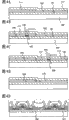
Figure 1A to 1E is the sectional view of the manufacturing process of explanation semiconductor device of the present invention;
Fig. 2 A to 2E is the sectional view of the manufacturing process of explanation semiconductor device of the present invention;
Fig. 3 A to 3E is the sectional view of the manufacturing process of explanation semiconductor device of the present invention;
Fig. 4 A to 4E is the sectional view of the manufacturing process of explanation semiconductor device of the present invention;
Fig. 5 A to 5D is the sectional view of the manufacturing process of explanation semiconductor device of the present invention;
Fig. 6 is the sectional view of creating conditions of explanation crystalline semiconductor film of the present invention;
Fig. 7 is the oblique view that explanation can be applied to laser aid of the present invention;
Fig. 8 is the oblique view of the high preferred orientation of explanation crystalline semiconductor film of the present invention;
Fig. 9 A to 9D is the sectional view of the manufacturing process of explanation semiconductor device of the present invention;
Figure 10 A to 10C is the sectional view of the manufacturing process of explanation semiconductor device of the present invention;
Figure 11 A to 11C is the sectional view of the manufacturing process of explanation semiconductor device of the present invention;
Figure 12 is the figure that explanation can be applied to the equivalent electric circuit of light-emitting component of the present invention;
Figure 13 A to 13E is the sectional view of the manufacturing process of explanation semiconductor device of the present invention;
Figure 14 A to 14D is the sectional view of the manufacturing process of explanation semiconductor device of the present invention;
Figure 15 A to 15C is the sectional view of the manufacturing process of explanation semiconductor device of the present invention;
Figure 16 A to 16D is the sectional view of the manufacturing process of explanation semiconductor device of the present invention;
Figure 17 is the figure of the structure of explanation semiconductor device of the present invention;
Figure 18 A to 18F is the figure of the purposes of explanation semiconductor device of the present invention;
Figure 19 A to 19F is the figure that the electronic equipment of semiconductor device of the present invention is used in explanation;
Figure 20 is the figure that the structure of the electronic equipment that uses semiconductor device of the present invention is described;
Figure 21 is the expanded view that the electronic equipment of semiconductor device of the present invention is used in explanation;
Figure 22 A and 22B are the vertical views of explanation semiconductor device of the present invention;
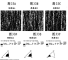
Figure 23 A to 23F is the distribution of orientations image of the expression crystalline silicon film of measuring the embodiment that has obtained by EBSP and the figure of orientation ratio;
Figure 24 A to 24F is the distribution of orientations image of the expression crystalline silicon film of measuring the embodiment that has obtained by EBSP and the figure of orientation ratio;
Figure 25 A to 25F is the distribution of orientations image of the expression crystalline silicon film of measuring the embodiment that has obtained by EBSP and the figure of orientation ratio;
Figure 26 A to 26F is the distribution of orientations image of the expression crystalline silicon film of measuring the embodiment that has obtained by EBSP and the figure of orientation ratio;
Figure 27 A to 27F is the distribution of orientations image of the expression crystalline silicon film of measuring the embodiment that has obtained by EBSP and the figure of orientation ratio;
Figure 28 A to 28F is the distribution of orientations image of the expression crystalline silicon film of measuring the embodiment that has obtained by EBSP and the figure of orientation ratio;
Figure 29 A to 29F is the distribution of orientations image of the expression crystalline silicon film of measuring the embodiment that has obtained by EBSP and the figure of orientation ratio;
Figure 30 A to 30F is the distribution of orientations image of the expression crystalline silicon film of measuring the embodiment that has obtained by EBSP and the figure of orientation ratio;
Figure 31 A to 31F is the distribution of orientations image of the expression crystalline silicon film of measuring the embodiment that has obtained by EBSP and the figure of orientation ratio;
Figure 32 A to 32F is the distribution of orientations image of the expression crystalline silicon film of measuring the embodiment that has obtained by EBSP and the figure of orientation ratio;
Figure 33 A to 33F is the distribution of orientations image of the expression crystalline silicon film of measuring the embodiment that has obtained by EBSP and the figure of orientation ratio;
Figure 34 A to 34F is the distribution of orientations image of the expression crystalline silicon film of measuring the embodiment that has obtained by EBSP and the figure of orientation ratio;
Figure 35 A to 35F is the distribution of orientations image of the expression crystalline silicon film of measuring the embodiment that has obtained by EBSP and the figure of orientation ratio.
Embodiment
Below, with reference to the description of drawings embodiments of the present invention.But, the present invention can implement by different ways, and it is exactly that its mode and detailed content can be transformed to various forms in not breaking away from aim of the present invention and scope thereof that the person of an ordinary skill in the technical field can understand a fact at an easy rate.Therefore, the present invention should not be interpreted as only being limited in the content that following execution mode puts down in writing.Notice that in whole accompanying drawings of explanation execution mode, same section or the part with identical function are represented by identical Reference numeral, and omitted repeat specification.
In the present embodiment, be described as follows the manufacture method of crystalline semiconductor film with reference to Figure 1A to 1E, Fig. 6 to Fig. 8, promptly, on amorphous semiconductor film, form coverlay, use the laser beam of continuous oscillation or repetition rate laser beam irradiation amorphous semiconductor film across this coverlay, make and have its surperficial high preferred orientation for { crystal of 001} and high preferred orientation are { 211} or { the crystalline semiconductor film of the crystal of 101} as the impulse hunting more than the 10MHz.
At first, shown in Figure 1A, like that, on a surface of substrate 100, form dielectric film 101 as basilar memebrane with insulating surface.The silicon oxide film, silicon nitride film, nitrogen content that as the dielectric film 101 of basilar memebrane by used thickness suitably are 50nm to 150nm are more than the formation such as oxygen silicon nitride membrane more than nitrogen content of the silicon oxynitride film of oxygen content and oxygen content.As the substrate 100 with insulating surface, for example used thickness is the glass substrate of 0.7mm.In addition, as the dielectric film 101 as basilar memebrane, forming thickness by plasma CVD method is the silicon oxynitride film of 50nm, and forming thickness by plasma CVD method then is the oxygen silicon nitride membrane of 100nm.
Noting, forms as required as the dielectric film 101 of basilar memebrane and get final product, in other words, is under the situation of glass at substrate 100, prevents diffusion of impurities from glass to semiconductor film 102, and is under the situation of quartz at substrate 100, does not need formation.In addition, also can between dielectric film 101 and substrate 100 stripping film be set, operation finishes the back from substrate 100 stripping semiconductor elements.
Next, forming thickness by plasma CVD method on dielectric film 101 is more than the 10nm and below the 100nm, is preferably 20nm is above and 80nm is following amorphous semiconductor film as semiconductor film 102.
As semiconductor film 102,, also can use SiGe (Si though use amorphous silicon in the present embodiment
1-xGe
x(0<x<0.1)) etc., the carborundum (SiC) of monocrystalline can also be used as diamond lattic structure.
In addition, be under the situation of amorphous semiconductor film at described semiconductor film 102, also can after forming semiconductor film 102, heat semiconductor film.Described heat treated is to be used for processing from the amorphous semiconductor film dehydrogenation.Notice that this dehydrogenation is handled in order to prevent that semiconductor film 102 sprays hydrogen and carries out when the illuminating laser beam, therefore, if the hydrogen that is included in the semiconductor film 102 is few, just can be omitted.Here, semiconductor film 102 was heated one hour in 500 ℃ electric furnace.
Though the example of amorphous silicon as semiconductor film 102 used in expression in the present embodiment, but also can use polysilicon, this polysilicon can form by the following method, promptly, for example after forming amorphous silicon film, this amorphous silicon film trace is added elements such as nickel, palladium, germanium, iron, tin, lead, cobalt, platinum, copper, gold, under 500 ℃ to 750 ℃ temperature, carry out one minute to ten hours heat treatment then.
Next, forming thickness on semiconductor film 102 is SiN more than the 200nm and below the 1000nm
xO
y(0≤x≤1.5,0≤y≤2,0≤4x+3y≤6) film is as coverlay 103.Note,,, just be not easy to control the high preferred orientation of the crystalline semiconductor film that the back will form, therefore be preferably formed and be the thickness more than the 200nm and below the 1000nm if thin excessively for described coverlay 103.
As coverlay 103, preferably, have enough transmitances with respect to the wavelength of laser beam, the hot value and the ductility equivalence of thermal coefficient of expansions etc. approach adjacent semiconductor film.In addition, coverlay 103 is preferably the similarly hard and slower careful film of etching speed of gate insulating film of the thin-film transistor that will form with the back.As an example, be preferably the mixed aqueous solution of the ammonium fluoride by using 7.13% ammonium acid fluoride and 15.4% or hydrofluoric acid aqueous solution under 20 ℃ the temperature with 1nm/min more than and below the 150nm/min, preferably with the careful film of the etch rate etch more than the 10nm/min and below the 130nm/min.In addition,, be preferably, preferably carry out the careful film of dry-etching with the etching speed more than the 110nm/min and below the 130nm/min by using hydrogen fluorohydrocarbon (HFC) gas with more than the 100nm/min and below the 150nm/min as an example.This hard and careful film for example can form by reducing rate of film build.Form careful film as coverlay 103 and make pyroconductivity improve, and prevent the excessive accumulation of heat that causes by the laser beam that shines coverlay and semiconductor film.Thereby, owing to can reduce the evaporation of semi-conductive melt, therefore can suppress the reduction of the viscosity of semi-conductive melt, make it possible to suppress the turbulent flow of semi-conductive melt.
In addition,, during illuminating laser beam, can reduce the evaporation of semi-conductive melt, can suppress the reduction of the viscosity of semi-conductive melt, make it possible to suppress the turbulent flow of semi-conductive melt when being formed with on the semiconductor film surface under the state of coverlay.In addition, owing to, fixed pressure is applied to semiconductor film, so can suppress the turbulent flow of semi-conductive melt by on the semiconductor film surface, forming coverlay.As a result, control the high preferred orientation of the crystal of crystalline semiconductor film easily.
Note, in coverlay, comprise under the situation of a lot of hydrogen, to carry out heat treated, so that dehydrogenation with the same mode of semiconductor film 102.
Next, shown in Figure 1B, use the part of first laser beam, 105 irradiation semiconductor films 102, forming its surperficial high preferred orientation is the { crystalline region 106 of 001}.Note, in crystalline region 106, its surperficial high preferred orientation for the ratio that crystal occupied of 001} be preferably four one-tenths more than and below the hundred per cent.
At this, the relation of the sweep speed of laser beam and power is described and the high preferred orientation on the crystalline semiconductor film surface that will form with reference to Fig. 6.In Fig. 6, transverse axis is represented the sweep speed of laser beam, and the longitudinal axis is represented the power of laser beam.
The sweep speed of first laser beam 105 and the relation of power are preferably the relation in the zone 141 of satisfying Fig. 6, in other words, the power of first laser beam 105 preferably is higher than the scope of formation small particle diameter crystal and is { the scope of the crystal of 211} less than the high preferred orientation that forms surface (sightingpiston A).As a result, the high preferred orientation that can form plane of crystal is the { crystalline region of 001}.Note, in crystalline region 106, the high preferred orientation of plane of crystal for the ratio of 001} be preferably four one-tenths more than and below the hundred per cent.When in crystalline region 106, the high preferred orientation of plane of crystal is for { ratio of 001} is more than four one-tenths and hundred per cent when following, do not hinder the orientation ratio height of the high preferred orientation of electron transfer, therefore, can improve the mobility of n channel-type thin-film transistor by using this crystal.
Note, when using first laser beam 105 to make the semiconductor film crystallization, can be respectively the direction of the scanning direction that is parallel to laser beam and be parallel to the surface and direction perpendicular to the scanning direction of laser beam on, and ratio hundred per cent below above with four one-tenth, preferably, form high preferred orientation crystal toward the direction with more than sixty percent and the ratio below the hundred per cent.In other words, in three faces that intersect, has the crystal of certain high preferred orientation more than can forming in certain proportion respectively.As a result, can form the polycrystalline zone that is similar to mono-crystalline structures.
Next, shown in Fig. 1 C, use the part of second laser beam, 108 irradiation semiconductor films 102, forming its surperficial high preferred orientation is { 211} or the { crystalline region 110 of 101}.Note, in crystalline region 110, its surperficial high preferred orientation for 211} or the crystal ratio of 101} be preferably four one-tenths more than and below the hundred per cent.
In addition, the sweep speed of second laser beam 108 and power can be included in the zone 142 of Fig. 6, in other words, the power of second laser beam 108 preferably is higher than the scope that forms the small particle diameter crystal or forms its surperficial high preferred orientation and is { the scope of the crystal of 001}, an and part that is lower than semiconductor film takes place by scope of ablating or the scope that forms the irregular big particle diameter crystal of high preferred orientation.As a result, the high preferred orientation that can form plane of crystal is the { crystalline region of 211}.Note, in crystalline region 110, the high preferred orientation of plane of crystal for the ratio of 211} be preferably four one-tenths more than and below the hundred per cent.When in crystalline region 110, the high preferred orientation of plane of crystal is for { ratio of 211} is more than four one-tenths and hundred per cent when following, do not hinder the orientation ratio height of the high preferred orientation of hole migration, therefore, can improve the mobility of p channel-type thin-film transistor by using this crystal.
In addition, the sweep speed of second laser beam 108 and power can be included in the zone 143 of Fig. 6, in other words, the power of second laser beam preferably is higher than the scope that forms the small particle diameter crystal, and a part that is lower than semiconductor film takes place by scope of ablating or the scope that forms the irregular big particle diameter crystal of high preferred orientation.As a result, the high preferred orientation that can form plane of crystal is the { crystalline region of 101}.Note, in crystalline region 110, the high preferred orientation of plane of crystal for the ratio of 101} be preferably four one-tenths more than and below the hundred per cent.When in crystalline region 110, the high preferred orientation of plane of crystal is for { ratio of 101} is more than four one-tenths and hundred per cent when following, do not hinder the orientation ratio height of the high preferred orientation of hole migration, therefore, can improve the mobility of p channel-type thin-film transistor by using this crystal.
Note, when using second laser beam 108 to make the semiconductor film crystallization, can be respectively in the direction of the scanning direction that is parallel to laser beam be parallel on the surface and direction of semiconductor film perpendicular to the scanning direction of laser beam, and ratio hundred per cent below above with four one-tenth, preferably, form high preferred orientation crystal toward the direction with more than sixty percent and the ratio below the hundred per cent.In other words, on three faces that intersect, has the crystal of certain high preferred orientation more than can forming in certain proportion respectively.As a result, can form the polycrystalline zone that is similar to mono-crystalline structures.
By above operation, shown in Fig. 1 D, can make have its surperficial high preferred orientation for the crystalline region 106 of 001}, with and the surface high preferred orientation be { 211} or { the crystalline semiconductor film of the crystalline region 110 of 101}.
Here, the optical system that is used for using the laser beam irradiation amorphous semiconductor film to come the laser oscillator of crystallization and forms beam spot is described.
As shown in Figure 7, as laser oscillator 11a and 11b, use respectively to have the laser oscillator that absorbs the wavelength more than tens % by semiconductor film 102.Typically, can use second harmonic or triple-frequency harmonics.Here, prepare the continuous oscillation laser (YVO that the summation maximum is output as 20W and utilizes LD (laser diode) to excite
4, second harmonic (wavelength is 532nm)).Not necessarily need to be defined in second harmonic, still, second harmonic is better than the more harmonic wave of high order aspect energy efficiency.
The laser power of Shi Yonging is { 001} and { 211} or { in the scope of the crystalline semiconductor film of 101} in the scope of melting semiconductor film fully and can forming its surperficial high preferred orientation in the present invention.When use was lower than the laser power of this scope, semiconductor film can not melt fully and the high preferred orientation that causes forming crystal is not consistent and have a crystalline semiconductor film of small particle diameter crystal towards certain certain direction.Therefore, under the situation of Fig. 7, prepare two laser oscillators, still,, can prepare a laser oscillator as long as output is enough.When use is higher than the laser power of this scope, in semiconductor film, produces many nucleus, and from this nucleus, produce irregular crystal growth, thereby form crystalline semiconductor film with uneven crystal grain position, size and high preferred orientation.
When using continuous oscillation laser radiation semiconductor film 102, energy is fed to semiconductor film 102 continuously, therefore, in case make semiconductor film be in molten condition, can keep this state.In addition, can move the solid phase and the liquid interface of semiconductor film, can form long in one direction crystal grain along this moving direction by scanning continuous oscillation laser.Use solid state laser to be because compare with gas laser etc., output has high stability and can expect stabilized treatment.
Note, be not limited to continuous oscillation laser, also can use repetition rate to be the pulsed oscillation laser more than the 10MHz.
When use has the pulsed oscillation laser of high repetition frequency, as long as being shorter than from semiconductor film, the pulse spacing of laser is melted to the time that semiconductor film solidifies, can make semiconductor film on whole film thickness direction, remain molten condition always.Therefore, can form the semiconductor film of forming by the crystal grain that the length of cross growth is long in one direction by moving of solid phase and liquid interface.
In the present embodiment, YVO
4Laser is used for laser oscillator 11a and 11b, still, also can use other continuous oscillation lasers and repetition rate to be the pulsed oscillation laser device more than the 10MHz.For example, as gas laser, there are Ar laser, Kr laser, CO
2Laser etc.As solid state laser, there are YAG laser, YLF Lasers device, YAlO
3Laser, GdVO
4Laser, KGW laser, KYW laser, alexandrite (alexandrite translates the alexandrite jewel again) laser, Ti: sapphire laser, Y
2O
3Laser, YVO
4Laser etc.And, there are ceramic laser for example YAG laser, Y
2O
3Laser, GdVO
4Laser, YVO
4Laser etc.As metal vapor laser, there is helium cadmium laser etc.
In addition, in laser oscillator 11a and laser oscillator 11b, can use TEM
00(single transverse mould) makes laser beam and penetrates, and can improve the energy uniformity of the linear beam spot that obtains by this method on illuminated surface, so be preferred.
The summary of using the optical treatment of these laser oscillator emitted laser is following such.From laser oscillator 11a and laser oscillator 11b respectively with identical energy emission of lasering beam 12a and laser beam 12b.Change the polarization direction from laser oscillator 11b emitted laser bundle 12b by wavelength plate 13, this is in order to use mutually different two laser beams in polarizer 14 synthetic polarization directions.
Making after laser beam 12b passes wavelength plate 13,, enter polarizer 14, and form laser beam 12 by this polarizer 14 synthesized laser beam 12a and laser beam 12b by speculum 22 reflections.At this moment, regulate wavelength plate 13 and polarizer 14, make the light that has passed wavelength plate 13 and polarizer 14 have suitable energy.Note, in the present embodiment, polarizer 14 is used for the synthetic of laser beam, still, also can use for example polarized light beam splitter etc. of other optical elements.
By speculum 15 reflections, and the cross section of this laser beam for example for example forms linear on illuminated surperficial 18 for the cylindrical lens 17 of 20mm for the cylindrical lens 16 of 150mm and focal length by focal length by the synthetic laser beams 12 of polarizer 14.Notice that cremasteric reflex mirror 15 gets final product corresponding to the situation that is provided with of the optical system of laser irradiation device.
At this moment, cylindrical lens 16 acts on the length direction that is formed on the beam spot on illuminated surperficial 18, and cylindrical lens 17 acts on its Width.Therefore, on illuminated surperficial 18, form length for example and be approximately the linear beam spot that 500 μ m and width are approximately 20 μ m.To note, though in the present embodiment, to use cylindrical lens in order forming beam spot linear,, the present invention is not limited to this, also can use for example spherical lens etc. of other optical elements.And the focal length of cylindrical lens is not limited to above-mentioned value, and can be provided with arbitrarily.
In addition, though in the present embodiment, use cylindrical lens 16 and 17 to carry out the shaping of laser beam,, also can provide separately laser beam to be extended to linear optical system and the optical system of fine optically focused on illuminated surface.For example, in order to obtain the linear cross section of laser beam, can use cylindrical lens array, diffraction optical element, optical waveguide etc.In addition, when using the rectangular laser medium, also can obtain the linear cross section of laser beam at launching phase.
In the present invention, such as mentioned above, can use ceramic laser.Owing to when using ceramic laser, can relatively freely carry out the shaping of laser medium, so ceramic laser is suitable for making this laser beam.Notice that it is narrow as much as possible to be preferably its width with the cross sectional shape of the laser beam of linear formation, make the density of the laser beam energy in the semiconductor film increase, therefore can shorten activity time.
Next, the illuminating method of laser beam is described.In order to be formed with the illuminated surperficial 18 of the semiconductor film 102 that covers by coverlay 103 with relative high speed operation, this is fixed to absorption type objective table 19.Absorption type objective table 19 can move to the XY direction on the plane parallel with illuminated surperficial 18 with Y-axis single shaft track 21 by X-axis single shaft track 20.Arrange absorption type objective table 19 in the length direction of the linear beam spot mode consistent with Y-axis.
Next, make illuminated surperficial 18 Widths along beam spot, promptly X-axis moves, and uses laser beam irradiation illuminated surperficial 18.Here, be more than the 10cm/sec and below the 100cm/sec with the sweep speed of X-axis single shaft track 20, and from two laser oscillators respectively with the energy emission of lasering beam more than the 2W and below the 15W, the laser output after synthetic is that 4W is above and below the 30W.Because of the irradiation of this laser beam forms the zone of the complete fusion of semiconductor, crystal growth in process of setting, thus can form crystalline semiconductor film of the present invention.
Note, from TEM
00The Energy distribution of the laser oscillator emitted laser bundle of mode generally is a Gaussian Profile.Can change the width in the zone that the controlled crystal grain of high preferred orientation at three face places being perpendicular to one another forms by the optical system that is used for laser beam irradiation.For example, by using lens arra for example cylindrical lens array or compound eye lenticule, diffraction optical element, optical waveguide etc., can make intensity of laser beam even.
By using the laser beam irradiation semiconductor film 102 of its intensity homogenizing, can be in the zone of the irradiation that is subjected to laser beam, form with the controlled crystal grain of high preferred orientation for the vertical direction on surface.
Note, though in the present embodiment, the mode of use by utilizing X-axis single shaft track 20 and Y-axis single shaft track 21 to move as illuminated surperficial 18 semiconductor film 102, but the present invention is not limited to this, can utilize following method as the scan method of laser beam: fixing illuminated surperficial 18 and the irradiation system moving method of the irradiation position of mobile laser beam; The irradiation position of fixed laser bundle and move illuminated surperficial 18 illuminated surperficial moving method; Perhaps make up the method for above-mentioned two kinds of methods.
Moreover as mentioned above like that because the Energy distribution of beam spot on long axis direction that is formed by above-mentioned optical system is Gaussian Profile, so the small particle diameter crystal is formed on the two ends of this Gaussian Profile, promptly has the part of low energy densities.So, can be by the part of intercepting laser beams such as the line of rabbet joint be provided in illuminated surperficial 18 front, so that only use the laser beam irradiation illuminated surperficial 18 of the energy of the controlled crystal of high preferred orientation with enough formation films surface; Perhaps wait and form pattern, so that laser beam only arrives the semiconductor film of the part of wanting to form the controlled crystal of high preferred orientation by the metal film that on coverlay 103, forms reflection lasering beam.
In addition, in order more effectively to utilize,, beam spot energy even ground is in the longitudinal direction distributed by using beam homogenizer for example lens arra or diffraction optical element etc. from laser oscillator 11a and laser oscillator 11b emitted laser bundle.In addition, can move Y-axis single shaft track 21 with the width of the crystalline semiconductor film that formed, and scan X-axis single shaft track 20 once more with predetermined speed.By repeating a series of this operation, the whole surface of crystallization semiconductor film effectively.
Then, remove coverlay, then, on the crystalline semiconductor film, apply resist, expose and this resist that develops, thereby resist is formed desirable shape by carrying out etching.In addition, the etching of using the resist that forms to carry out the crystalline semiconductor film as mask here forms the crystalline semiconductor film of reservation shape.Then, remove Etching mask.
By above-mentioned operation, can form its surperficial high preferred orientation for 001} and have reservation shape the crystalline semiconductor film, with and the high preferred orientation on surface be { 211} or { 101} and have the crystalline semiconductor film of reservation shape.
Note, also can carry out the filming of crystalline semiconductor film before coating resist on the crystalline semiconductor film.Typically, also can carry out etching, so that the thickness on the whole surface of crystalline semiconductor film is more than the 10nm and below the 30nm.Moreover, also can on the crystalline semiconductor film, apply resist, form resist by exposure and development with desirable shape, with this resist is mask, the crystalline semiconductor film is etched to desirable shape, has the filming of the crystalline semiconductor film of desirable shape then.Particularly, also can carry out etching, be more than the 10nm and below the 30nm so that have the thickness of the crystalline semiconductor film of desirable shape.Because when the crystalline semiconductor film that uses such thin thickness formed thin-film transistor, thin-film transistor was that channel formation region is the transistor of complete depletion type, therefore can make the high thin-film transistor of mobility.
Next, shown in Fig. 1 E, use its surperficial high preferred orientation for { 001} and the crystalline semiconductor film with reservation shape are made n channel-type thin-film transistor 150, and use its surperficial high preferred orientation to be { 211} or { 101} and the crystalline semiconductor film with reservation shape are made p channel-type thin-film transistor 151.
Next, the high preferred orientation of the crystalline semiconductor film of making by present embodiment is described.In the present embodiment, can carry out EBSP (Electron Back-Scattered Diffraction pattern) to the high preferred orientation of the crystal grain of the crystalline semiconductor film of removing coverlay by etching measures.At first, the basic item of EBSP is described, then when adding supplementary notes, explains its result.
EBSP is meant following method, promptly, connect the EBSP detector to scanning electron microscope (SEM), analyze the direction of the diffraction image (EBSP image) of each crystal that when use convergence electron beam is radiated at the sample of high inclination in the scanning electron microscope, produces, and positional information (x, y) high preferred orientation of the crystal of working sample according to its bearing data and measurement point.
When making electron ray enter the crystalline semiconductor film, inelastic scattering also takes place overleaf, and also can observe the distinctive linear pattern of crystal high preferred orientation of Bragg diffraction in sample.Here, this linear pattern generally is called Kikuchi lines.The EBSP method is reflected in the high preferred orientation that Kikuchi lines in the detector obtains the crystal of crystalline semiconductor film by analysis.
In general, in having the sample of polycrystalline structure, each crystal grain has different high preferred orientations.Therefore, when the irradiation position of mobile crystalline semiconductor film, use electron ray irradiation sample, and analyze the crystal high preferred orientation on each irradiation position.So, can obtain to have the crystal high preferred orientation or the orientation information of the crystalline semiconductor film of flat surface.Because measured zone is wide more, can obtain the trend of the crystal high preferred orientation of many more crystalline semiconductor film integral body, so measurement point is many more, can get over the information of the crystal high preferred orientation that at length obtains in the measured zone.
In the present embodiment in the crystalline semiconductor film of Xing Chenging, following vector a to c and the sightingpiston A to C of setting like that.Vector a is vertical with substrate surface and vector C, scanning direction of vector C and laser beam (that is, the direction of growth of crystal grain) and substrate surface are parallel, and vector b is parallel with substrate surface and vertical with the direction of growth of crystal grain, in other words, vector b is perpendicular to one another with vector a and vector C.
In addition, as shown in Figure 8, be respectively that three faces of normal vector are set at sightingpiston A, sightingpiston B and sightingpiston C respectively with three vectors (vector a, vector b and vector C) that are perpendicular to one another.
In the present embodiment, the control vector a vertical with substrate surface and vector C be normal vector sightingpiston A (promptly, the growth of the crystal high preferred orientation the surface of crystalline semiconductor film) forms and has { the crystalline region of the high preferred orientation of 001} and have { 211} or the { crystalline region of the high preferred orientation of 101}.
Therefore, the high preferred orientation of crystals can not only be determined according to the high preferred orientation that obtains by a sightingpiston measuring crystal.This be because, even only on a sightingpiston high preferred orientation if high preferred orientation is inconsistent on other sightingpistons, can not say the cause of the high preferred orientation unanimity of its crystals towards a direction unanimity.Therefore, according to the high preferred orientation at least two surfaces, moreover many more according to the information of multilist face more, the precision of the high preferred orientation of crystals increases more.
In other words, all be uniformly if distribute at the high preferred orientation of measuring interior three faces in zone, just this can be regarded as the near single body.Therefore, can be according to the information of these three sightingpiston A to C, particular crystal high preferred orientation accurately.
On semiconductor film, form coverlay, use then the laser beam of continuous oscillation or repetition rate as the laser beam of the impulse hunting more than the 10MHz across this coverlay irradiation semiconductor film, the high preferred orientation that can form sightingpiston A is for { high preferred orientation of the crystalline region of 001} and sightingpiston A is { 211} or the { crystalline region of 101}.
The high preferred orientation of sightingpiston A is for { crystalline region of 001} has the high preferred orientation of the electron transfer of not hindering, and the high preferred orientation of sightingpiston A is { 211} or { crystalline region of 101} has the high preferred orientation of the hole migration of not hindering.Therefore, { crystalline region of 001} is made n type thin-film transistor to use the high preferred orientation of sightingpiston A to be, and the high preferred orientation that uses sightingpiston A is { 211} or { the crystalline region manufacturing p type thin-film transistor of 101}, the next semiconductor device that can make raising mobility separately.
Execution mode 2
In the present embodiment, is that { high preferred orientation of the crystalline region of 001} and sightingpiston A is { 211} or the { method of the crystalline semiconductor film of the crystalline region of 101} with reference to Fig. 2 A to 2E explanation by adopting the structure of coverlay different from the embodiment described above, make the high preferred orientation with sightingpiston A.
Same with execution mode 1, shown in Fig. 2 A, on a surface of substrate 100, form dielectric film 101 as basilar memebrane with insulating surface.Then, forming thickness by plasma CVD method on dielectric film 101 is more than the 10nm and below the 100nm, is preferably 20nm is above and 80nm is following amorphous semiconductor film as semiconductor film 102.
In addition, also can after forming semiconductor film 102, in 500 ℃ electric furnace, heat one hour.Described heat treated is to be under the situation of amorphous semiconductor film at semiconductor film 102, is used for from the processing of this amorphous semiconductor film dehydrogenation.Notice that this dehydrogenation is handled in order to prevent that semiconductor film 102 sprays hydrogen and carries out when the illuminating laser beam, therefore, if the hydrogen that is included in the semiconductor film 102 is few, just can be omitted.
Next, laminated cover film 103a, 103b on semiconductor film 102.The summation thickness of coverlay 103a, 103b is preferably more than the 200nm and below the 1000nm.In addition, the thickness that is contacted with the coverlay 103a of semiconductor film 102 is preferably more than the 50nm.This is because following cause, that is, under the situation of thickness of the coverlay 103a that is contacted with semiconductor film 102, when using laser beam irradiation semiconductor film 102 less than 50nm, coverlay 103a is melted in the semiconductor film 102, and the quality of coverlay changes along with the film thickness change of semiconductor film.
As coverlay 103a, 103b, form respectively and form mutually different SiN
xO
y(0≤x≤1.5,0≤y≤2,0≤4x+3y≤6) film.In the present embodiment, forming thickness as coverlay 103a is the SiN of 100nm
xO
y(film of x>y), forming thickness as coverlay 103b is the SiN of 300nm
xO
y(the film of x<y).Note, comprise at coverlay 103a, 103b under the situation of a lot of hydrogen, similarly be used for the heat treated of dehydrogenation with semiconductor film 102.
Next, shown in Fig. 2 B, use the part of first laser beam 105 from coverlay 103a, 103b one side irradiation semiconductor film 102, the high preferred orientation that forms sightingpiston A is the { crystalline region 106 of 001}.Note, in crystalline region 106, the high preferred orientation of crystal the ratio of 001} be preferably four one-tenths more than and below the hundred per cent.
Note, when using first laser beam 105 shown in the execution mode 1 to carry out the crystallization of semiconductor film 102, can be respectively with more than four one-tenth and below the hundred per cent in sightingpiston B and sightingpiston C, preferably with more than sixty percent and the ratio below the hundred per cent form high preferred orientation crystal toward the direction.In other words, can in sightingpiston A, B and C, form respectively, preferably to have the crystal of certain high preferred orientation more than sixty percent and below the hundred per cent with more than four one-tenth and below the hundred per cent.
Next, shown in Fig. 2 C, use the part of second laser beam 108 shown in the execution mode 1 from coverlay 103a, 103b one side irradiation semiconductor film 102, the high preferred orientation that forms sightingpiston A is { 211} or the { crystalline region 110 of 101}.Note, in crystalline region 110, the high preferred orientation of crystal 211} or the ratio of 101} be preferably four one-tenths more than and below the hundred per cent.
Note, when using second laser beam shown in the execution mode 1 to carry out the crystallization of semiconductor film, can be respectively with more than four one-tenth and below the hundred per cent in sightingpiston B and sightingpiston C, preferably with more than sixty percent and the ratio below the hundred per cent form high preferred orientation crystal toward the direction.In other words, can in sightingpiston A, B and C, form respectively, preferably to have the crystal of certain high preferred orientation more than sixty percent and below the hundred per cent with more than four one-tenth and below the hundred per cent.
By above-mentioned operation, shown in Fig. 2 D, can make the high preferred orientation with sightingpiston A is that { crystalline region 106 of 001} and the high preferred orientation of sightingpiston A are { 211} or { the crystalline semiconductor film of the crystalline region 110 of 101}.
Then, remove coverlay, then, on the crystalline semiconductor film, apply resist, expose and this resist that develops, thereby resist is formed desirable shape by carrying out etching.In addition, the etching of using the resist that forms to carry out the crystalline semiconductor film as mask here forms the crystalline semiconductor film of reservation shape.Then, remove Etching mask.
Note, also can similarly carry out the filming of crystalline semiconductor film with execution mode 1.Typically, also can carry out etching, so that the thickness on the whole surface of crystalline semiconductor film is more than the 10nm and below the 30nm.Because when the crystalline semiconductor film that uses such thin thickness formed thin-film transistor, transistor became the thin-film transistor that channel formation region is complete depletion type, therefore can make the high thin-film transistor of mobility.
By above-mentioned operation, the high preferred orientation that can form sightingpiston A is { 001} and have the crystalline semiconductor film of reservation shape and the high preferred orientation of sightingpiston A is { 211} or { 101} and have the crystalline semiconductor film of reservation shape.
Next, shown in Fig. 2 E, the high preferred orientation that uses sightingpiston A is for { 001} and the crystalline semiconductor film with reservation shape are made n channel-type thin-film transistor 150, and the high preferred orientation that uses sightingpiston A is { 211} or { 101} and the crystalline semiconductor film with reservation shape are made p channel-type thin-film transistor 151.
By above-mentioned operation, on semiconductor film, form coverlay, use then the laser beam of continuous oscillation or repetition rate as the laser beam of the impulse hunting more than the 10MHz across this coverlay irradiation semiconductor film, the high preferred orientation that can form sightingpiston A is for { high preferred orientation of the crystalline region of 001} and sightingpiston A is { 211} or the { crystalline region of 101}.
The high preferred orientation of sightingpiston A is for { crystalline region of 001} has the high preferred orientation of the electron transfer of not hindering, and the high preferred orientation of sightingpiston A is { 211} or { crystalline region of 101} has the high preferred orientation of the hole migration of not hindering.Therefore, { crystalline region of 001} is made n type thin-film transistor to use the high preferred orientation of sightingpiston A to be, and the high preferred orientation that uses sightingpiston A be { 211} or { crystalline region of 101} is made p type thin-film transistor, can make the semiconductor device that has improved mobility separately.
Execution mode 3
In the present embodiment, is that { high preferred orientation of the crystal of 001} and sightingpiston A is { 211} or the { method of the crystalline semiconductor film of the crystal of 101} with reference to Fig. 3 A to 3E explanation by adopting the structure of coverlay different from the embodiment described above, make the high preferred orientation with sightingpiston A.
Same with execution mode 1, as shown in Figure 3A, on a surface of substrate 100, form dielectric film 101 as basilar memebrane with insulating surface.Then, forming thickness by plasma CVD method on dielectric film 101 is more than the 10nm and below the 100nm, is preferably 20nm is above and 80nm is following amorphous semiconductor film as semiconductor film 102.
In addition, also can after forming semiconductor film 102, in 500 ℃ electric furnace, heat one hour.Described heat treated is to be used for processing from the amorphous semiconductor film dehydrogenation.Notice that this dehydrogenation is handled in order to prevent semiconductor film 102 ejection hydrogen when using laser beam irradiation and carried out, and therefore, if the hydrogen that is included in the semiconductor film 102 is few, just can be omitted.
Next, on semiconductor film 102, form coverlay 111,112 with reservation shape.The thickness of coverlay 111,112 is preferably respectively more than the 200nm and below the 1000nm.In addition, as coverlay 111,112, form respectively and form mutually different SiN
xO
y(0≤x≤1.5,0≤y≤2,0≤4x+3y≤6) film.When using SiN as coverlay
xO
y(during the film of x>y), be { the crystal of 001} than being easier in sightingpiston A, preferentially to form high preferred orientation.On the other hand, when using SiN as coverlay
xO
y(during the film of x<y), be { 211} or the { crystal of 101} than being easier in sightingpiston A, preferentially to form high preferred orientation.Therefore, preferably to form in the back in the zone of n channel-type thin-film transistor and form SiN
xO
y(film of x>y) is as coverlay 111, forms SiN and will form in the back in the zone of p channel-type thin-film transistor
xO
y(film of x<y) is as coverlay 112.
On the whole surface of amorphous semiconductor film, form SiN by plasma CVD method etc.
xO
y(x>y) and SiN
xO
y(side among the x<y) is that mask is with SiN with the resist that forms by photoetching process then
xO
y(x>y) and SiN
xO
y(side among the x<y) is etched to desirable shape, forms coverlay 111.Then, on coverlay 111 and amorphous semiconductor film, form SiNxOy (x>y) and SiN
xO
y(the opposing party among the x<y) is that mask is with SiN with the resist that forms by photoetching process then
xO
y(x>y) and SiN
xO
y(the opposing party among the x<y) is etched to desirable shape, forms coverlay 112.Note, at this moment, be preferably formed with coverlay 112 and compare the slow film of etching speed as coverlay 111.As a result, can be at etching SiN
xO
y(x>y) and SiN
xO
y(in the time of the opposing party among the x<y), make SiN
xO
y(x>y) and SiN
xO
y(side among the x<y) is residual.
Note, in coverlay 111,112, comprise under the situation of a lot of hydrogen, similarly be used for the heat treated of dehydrogenation with semiconductor film 102.
Next, shown in Fig. 3 B, use the part of first laser beam 105 shown in the execution mode 1 from coverlay 111 1 sides irradiation semiconductor film 102, the high preferred orientation that forms sightingpiston A is the { crystalline region 106 of 001}.Note, in crystalline region 106, the high preferred orientation of the sightingpiston A of crystal the ratio of 001} be preferably four one-tenths more than and below the hundred per cent.
Note, when using first laser beam 105 shown in the execution mode 1 to carry out the crystallization of semiconductor film, can be respectively with more than four one-tenth and below the hundred per cent in sightingpiston B and sightingpiston C, preferably with more than sixty percent and the ratio below the hundred per cent form high preferred orientation crystal toward the direction.In other words, can in sightingpiston A, B and C, form respectively, preferably to have the crystal of certain high preferred orientation more than sixty percent and below the hundred per cent with more than four one-tenth and below the hundred per cent.
Next, shown in Fig. 3 C, use the part of second laser beam 108 shown in the execution mode 1 from coverlay 112 1 sides irradiation semiconductor film 102, the high preferred orientation that forms sightingpiston A is { 211} or the { crystalline region 110 of 101}.Note, in crystalline region 110, the high preferred orientation of crystal 211} or the ratio of 101} be preferably four one-tenths more than and below the hundred per cent.
Note, when using second laser beam shown in the execution mode 1 to carry out the crystallization of semiconductor film, can be respectively with more than four one-tenth and below the hundred per cent in sightingpiston B and sightingpiston C, preferably with more than sixty percent and the ratio below the hundred per cent form high preferred orientation crystal toward the direction.In other words, can in sightingpiston A, B and C, form respectively, preferably to have the crystal of certain high preferred orientation more than sixty percent and below the hundred per cent with more than four one-tenth and below the hundred per cent.
By above-mentioned operation, shown in Fig. 3 D, can make the high preferred orientation with sightingpiston A is that { crystalline region 106 of 001} and the high preferred orientation of sightingpiston A are { 211} or { the crystalline semiconductor film of the crystalline region 110 of 101}.
Then, remove coverlay 111,112, then, on the crystalline semiconductor film, apply resist, expose and this resist that develops, thereby resist is formed desirable shape by carrying out etching.In addition, the etching of using the resist that forms to carry out the crystalline semiconductor film as mask here forms the crystalline semiconductor film of reservation shape.Then, remove Etching mask.
Note, also can similarly carry out the filming of crystalline semiconductor film with execution mode 1.Typically, also can carry out etching, so that the thickness on the whole surface of crystalline semiconductor film is more than the 10nm and below the 30nm.Because when the crystalline semiconductor film that uses such thin thickness formed thin-film transistor, transistor became the thin-film transistor that channel formation region is complete depletion type, therefore can make the high thin-film transistor of mobility.
By above-mentioned operation, the high preferred orientation that can form sightingpiston A is { 001} and have the crystalline semiconductor film of reservation shape and the high preferred orientation of sightingpiston A is { 211} or { 101} and have the crystalline semiconductor film of reservation shape.
Next, shown in Fig. 3 E, the high preferred orientation that uses sightingpiston A is for { 001} and the crystalline semiconductor film with reservation shape are made n channel-type thin-film transistor 150, and the high preferred orientation that uses sightingpiston A is { 211} or { 101} and the crystalline semiconductor film with reservation shape are made p channel-type thin-film transistor 151.
Shown in present embodiment, on semiconductor film, form coverlay, use then the laser beam of continuous oscillation or repetition rate as the laser beam of the impulse hunting more than the 10MHz across this coverlay irradiation semiconductor film, the high preferred orientation that can form sightingpiston A is for { high preferred orientation of the crystalline region of 001} and sightingpiston A is { 211} or the { crystalline region of 101}.
The high preferred orientation of sightingpiston A is for { crystalline region of 001} has the high preferred orientation of the electron transfer of not hindering, and the high preferred orientation of sightingpiston A is { 211} or { crystalline region of 101} has the high preferred orientation of the hole migration of not hindering.Therefore, { crystalline region of 001} is made n type thin-film transistor to use the high preferred orientation of sightingpiston A to be, and the high preferred orientation that uses sightingpiston A is { 211} or { the crystalline region manufacturing p type thin-film transistor of 101}, the next semiconductor device that can make raising mobility separately.
Execution mode 4
In the present embodiment, is that { high preferred orientation of the crystal of 001} and sightingpiston A is { 211} or the { method of the crystalline semiconductor film of the crystal of 101} with reference to Fig. 4 A to 4E explanation by adopting the structure of coverlay different from the embodiment described above, make the high preferred orientation with sightingpiston A.
Same with execution mode 1, shown in Fig. 4 A, on a surface of substrate 100, form dielectric film 101 as basilar memebrane with insulating surface.Then, forming thickness by plasma CVD method on dielectric film 101 is more than the 10nm and below the 100nm, is preferably 20nm is above and 80nm is following amorphous semiconductor film as semiconductor film 102.
In addition, also can after forming semiconductor film 102, in 500 ℃ electric furnace, heat one hour.Described heat treated is to be used for processing from the amorphous semiconductor film dehydrogenation.Notice that this dehydrogenation is handled in order to prevent semiconductor film 102 ejection hydrogen when using laser beam irradiation and carried out, and therefore, if the hydrogen that is included in the semiconductor film 102 is few, just can be omitted.
Next, on semiconductor film 102, form coverlay 111, then, on this coverlay 111 and semiconductor film 102, form coverlay 113 with reservation shape.The thickness of coverlay 111 is preferably more than the 200nm and below the 500nm.The thickness of coverlay 113 is preferably more than the 200nm and below the 500nm.In addition, as coverlay 111,113, form respectively and form mutually different SiN
xO
y(0≤x≤1.5,0≤y≤2,0≤4x+3y≤6) film.By laminated cover film, because of the multilayer film interference effect absorbs heat in the semiconductor film with changing actual effect, so the melting time of semiconductor film also changes.As a result, can control the crystal high preferred orientation of crystalline semiconductor film.
When using SiN as coverlay
xO
y(during the film of x>y), preferentially forming high preferred orientation easily in sightingpiston A is the { crystal of 001}.On the other hand, when using SiN as coverlay
xO
y(during the film of x<y), preferentially forming high preferred orientation easily in sightingpiston A is { 211} or the { crystal of 101}.Therefore, preferably to form in the back to form in the zone of n channel-type thin-film transistor and have the SiN that nitrogen is higher than the ratio of components of oxygen
xO
yFilm is as coverlay 111, has the SiN that oxygen is higher than the ratio of components of nitrogen and will form in the back to form in the zone of p channel-type thin-film transistor
xO
yFilm is as coverlay 113.
On the whole surface of amorphous semiconductor film, form SiN by plasma CVD method etc.
xO
y(x>y) and SiN
xO
y(side among the x<y) is that mask is with SiN with the resist that forms by photoetching process then
xO
y(x>y) and SiN
xO
y(side among the x<y) is etched to desirable shape, forms coverlay 111.Then, on coverlay 111 and amorphous semiconductor film, form SiN
xO
y(x>y) and SiN
xO
y(the opposing party among the x<y) forms coverlay 113.Notice, at this moment, be preferably formed with coverlay 113 and compare that the slow film of etching speed is as coverlay 111.
About the coverlay in the present embodiment, side's coverlay (being coverlay 111 here) is formed reservation shape, the opposing party's coverlay (being coverlay 113 here) is formed on the top integral body of substrate and does not form reservation shape.Therefore, compare, can reduce operation quantity with execution mode 3.
Note, in coverlay 111,113, comprise under the situation of a lot of hydrogen, similarly be used for the heat treated of dehydrogenation with semiconductor film 102.
Next, shown in Fig. 4 B, use the part of first laser beam 105 from coverlay 111,113 1 sides irradiation semiconductor film 102, the high preferred orientation that forms sightingpiston A is the { crystalline region 106 of 001}.Note, in crystalline region 106, the high preferred orientation of the sightingpiston A of crystal the ratio of 001} be preferably four one-tenths more than and below the hundred per cent.
Note, when using first laser beam shown in the execution mode 1 to carry out the crystallization of semiconductor film, can be respectively with more than four one-tenth and below the hundred per cent in sightingpiston B and sightingpiston C, preferably with more than sixty percent and the ratio below the hundred per cent form high preferred orientation crystal toward the direction.In other words, the crystal that has certain high preferred orientation more than can in sightingpiston A, B and C, forming in certain proportion respectively.
Next, shown in Fig. 4 C, use the part of second laser beam 108 from coverlay 113 1 sides irradiation semiconductor film 102, the high preferred orientation that forms sightingpiston A is { 211} or the { crystalline region 110 of 101}.Note, in crystalline region 110, the high preferred orientation of crystal 211} or the ratio of 101} be preferably four one-tenths more than and below the hundred per cent.
Note, when using second laser beam 108 shown in the execution mode 1 to carry out the crystallization of semiconductor film, can be respectively with more than four one-tenth and below the hundred per cent in sightingpiston B and sightingpiston C, preferably with more than sixty percent and the ratio below the hundred per cent form high preferred orientation crystal toward the direction.In other words, the crystal that has certain high preferred orientation more than can in sightingpiston A, B and C, forming in certain proportion respectively.
By above-mentioned operation, shown in Fig. 4 D, can make the high preferred orientation with sightingpiston A is that { crystalline region 106 of 001} and the high preferred orientation of sightingpiston A are { 211} or { the crystalline semiconductor film of the crystalline region 110 of 101}.
Then, remove coverlay 111,113, then, on the crystalline semiconductor film, apply resist, expose and this resist that develops, thereby resist is formed desirable shape by carrying out etching.In addition, the etching of using the resist that forms to carry out the crystalline semiconductor film as mask here forms the crystalline semiconductor film of reservation shape.Then, remove Etching mask.
Note, also can similarly carry out the filming of crystalline semiconductor film with execution mode 1.Typically, also can carry out etching, so that the thickness on the whole surface of crystalline semiconductor film is more than the 10nm and below the 30nm.Because when the crystalline semiconductor film that uses such thin thickness formed thin-film transistor, transistor became the thin-film transistor that channel formation region is complete depletion type, therefore can make the high thin-film transistor of mobility.
By above-mentioned operation, the high preferred orientation that can form sightingpiston A is { 001} and have the crystalline semiconductor film of reservation shape and the high preferred orientation of sightingpiston A is { 211} or { 101} and have the crystalline semiconductor film of reservation shape.
Next, shown in Fig. 4 E, the high preferred orientation that can use sightingpiston A is for { 001} and the crystalline semiconductor film with reservation shape are made n channel-type thin-film transistor 150, and the high preferred orientation that uses sightingpiston A is { 211} or { 101} and the crystalline semiconductor film with reservation shape are made p channel-type thin-film transistor 151.
By above-mentioned operation, on semiconductor film, form coverlay, use then the laser beam of continuous oscillation or repetition rate as the laser beam of the impulse hunting more than the 10MHz across this coverlay irradiation semiconductor film, the high preferred orientation that can form sightingpiston A is for { high preferred orientation of the crystalline region of 001} and sightingpiston A is { 211} or the { crystalline region of 101}.
The high preferred orientation of sightingpiston A is for { crystalline region of 001} has the high preferred orientation of the electron transfer of not hindering, and the high preferred orientation of sightingpiston A is { 211} or { crystalline region of 101} has the high preferred orientation of the hole migration of not hindering.Therefore, { crystalline region of 001} is made n type thin-film transistor to use the high preferred orientation of sightingpiston A to be, and the high preferred orientation that uses sightingpiston A be { 211} or { crystalline region of 101} is made p type thin-film transistor, can make the semiconductor device that has improved mobility separately.
In the present embodiment, illustrate that with reference to Fig. 6 can make high preferred orientation in the sightingpiston A shown in the above-mentioned execution mode is that { crystalline region of 001}, high preferred orientation are for { crystalline region of 211} and high preferred orientation are { power of the laser beam of the crystalline region of 101} and sweep speed.
Here, the dielectric film as basilar memebrane forms the SiN that thickness is 50nm by plasma CVD method on substrate
xO
y(film of x>y), then, forming thickness by plasma CVD method is the SiN of 100nm
xO
y(the film of x<y).Then, forming thickness by plasma CVD method on dielectric film is the amorphous silicon film of 66nm.
After forming semiconductor film, be used for from the heat treatment of amorphous silicon film dehydrogenation, on semiconductor film, form coverlay then.As coverlay, forming thickness is the SiN of 400nm
xO
y(film of x>y) or thickness are the SiN of 500nm
xO
y(the film of x<y).Mixed solution or hydrofluoric acid aqueous solution when the ammonium fluoride that uses 7.13% ammonium acid fluoride and 15.4%, under 20 ℃ temperature during the described coverlay of etching, for example, its etching speed is more than the 1nm/min and below the 150nm/min, is preferably more than the 10nm/min and below the 130nm/min.In addition, as an example, the etched etching speed that uses hydrogen fluorohydrocarbon (HFC) gas is preferably more than the 110nm/min and below the 130nm/min as more than the 100nm/min and below the 150nm/min.Note, when forming SiN as coverlay
xO
y(during the film of x>y), be that reacting gas forms by plasma CVD method with monosilane and ammonia.In addition, when forming SiN as coverlay
xO
y(during the film of x<y), be that reacting gas forms by plasma CVD method with monosilane, ammonia and nitrous oxide.
Notice that when forming coverlay, because of the multilayer film interference effect changes the absorptivity of semiconductor film, certainly, the absorptivity of this semiconductor film also changes according to the film thickness of coverlay.In addition, in general, the absorption coefficient of light of semiconductor film is different between solid state and melt state, and both difference are more little, and the laser power permissible range of lateral crystal growth is big more.In other words, be subjected to the irradiation of laser beam at the semiconductor film of solid state, and the moment of this semiconductor film fusion, under the situation that absorptivity sharply raises, semiconductor film is ablated easily.Therefore, the laser power among Fig. 6 is with respect to the film thickness of semiconductor film and coverlay and to change be self-evident.
Then, use continuous oscillation or repetition rate to shine amorphous silicon film across coverlay as the laser beam of the impulse hunting more than the 10MHz.The relation table of the high preferred orientation of the sightingpiston A of the sweep speed of laser beam of this moment and power and the crystalline silicon film that will form is shown in Fig. 6.
In Fig. 6, transverse axis is represented the sweep speed of laser beam, and the longitudinal axis is represented the power of laser beam.Notice that in the Gaussian Profile of laser beam at this moment, use the line of rabbet joint to remove the uneven part of Energy distribution, the area of beam spot is 500 μ m * 20 μ m.
In sightingpiston A, can form high preferred orientation for { scope of the power of the laser beam of the crystal of 001} is the { power of the laser beam of the crystal of 211} greater than the power of the laser beam that forms little crystal grain and less than make high preferred orientation in sightingpiston A.In other words, in the sweep speed x of laser beam is part more than the 10cm/sec and below the 20cm/sec, described scope is equivalent to satisfy formula more than 1 and less than the power y of the laser beam of formula 2, this formula 1 expression can formation high preferred orientation is for { power of the laser beam of the crystal of 001}, this formula 2 are illustrated in and make high preferred orientation among the sightingpiston A and be { the upper limit of the crystal of 001} and to make high preferred orientation be the { power of the laser beam between the lower limit of the crystal of 211}.In addition, in the sweep speed x of laser beam is part more than the 20cm/sec and below the 35cm/sec, described scope is equivalent to satisfy formula more than 1 and less than the power y of the laser beam of formula 3, and this formula 3 is illustrated in to be made high preferred orientation and be { the upper limit of the crystal of 001} and to make high preferred orientation be the { power of the laser beam between the lower limit of the crystal of 211} among the sightingpiston A.
Y=0.0012x
2+ 0.083x+4.4 (formula 1)
Y=0.28x+4.2 (formula 2)
Y=-0.0683x+11.167 (formula 3)
In sightingpiston A, can form high preferred orientation for { scope of the power of the laser beam of the crystal of 211} is for being { the power of the laser beam of the crystal of 001}, and less than producing conditioned disjunction that film the ablates power less than the laser beam of the irregular crystalline semiconductor film of high preferred orientation that forms big particle diameter greater than the power of the laser beam that forms little crystal grain or greater than make high preferred orientation in sightingpiston A.
In other words, in the sweep speed x of laser beam is part more than the 10cm/sec and below the 20cm/sec, described scope is equivalent to satisfy the power y of the laser beam below 4 greater than formula 2 and formula, and this formula 4 is illustrated in, and can to make high preferred orientation among the sightingpiston A be the { power of the laser beam of the crystal of 211}.In addition, in the sweep speed of laser beam was part more than the 20cm/sec and below the 35cm/sec, described scope was equivalent to satisfy the power y of the laser beam below 4 greater than formula 3 and formula.In the sweep speed of laser beam is part more than the 35cm/sec and below the 55cm/sec, described scope is equivalent to satisfy formula more than 1 and the power y of the laser beam of formula below 5, and described formula 5 is illustrated in, and can to make high preferred orientation among the sightingpiston A be { the power y of the laser beam of the crystal of 211}.
Y=0.0027x
2+ 0.36x+4.2 (formula 4)
Y=-0.37x+33 (formula 5)
In sightingpiston A, can form high preferred orientation for { scope of the power of the laser beam of the crystal of 101} is greater than the power of the laser beam that forms little crystal grain and less than producing the condition that film is ablated, or less than the power of the laser beam of the irregular crystalline semiconductor film of high preferred orientation that forms big particle diameter.
In other words, in the sweep speed x of laser beam was part more than the 70cm/sec and below the 90cm/sec, described scope was equivalent to satisfy formula more than 1 and less than producing conditioned disjunction that film the ablates power y less than the laser beam of the irregular crystalline semiconductor film of high preferred orientation that forms big particle diameter.
By optionally shining the laser beam of above-mentioned power and sweep speed, can optionally form high preferred orientation for { crystalline region of 001} and high preferred orientation are the { crystalline region of 211}, optionally form high preferred orientation for { crystalline region of 001} and high preferred orientation are the { crystalline region of 101}, and optionally form high preferred orientation for { crystalline region of 001}, high preferred orientation are for { crystalline region of 211} and high preferred orientation are the { crystalline region of 101}.
The high preferred orientation of sightingpiston A is for { crystalline region of 001} has the high preferred orientation of the electron transfer of not hindering, and the high preferred orientation of sightingpiston A is { 211} or { crystalline region of 101} has the high preferred orientation of the hole migration of not hindering.Therefore, { crystalline region of 001} is made n type thin-film transistor to use the high preferred orientation of sightingpiston A to be, and the high preferred orientation that uses sightingpiston A be { 211} or { crystalline region of 101} is made p type thin-film transistor, can make the semiconductor device that has improved mobility separately.
Execution mode 6
In the present embodiment, be described below semiconductor film and manufacture method thereof, that is, on amorphous semiconductor film, form SiN with reference to Fig. 5 A to 5D
xO
y(coverlay of x<y), use the laser beam of continuous oscillation or repetition rate as the laser beam of the impulse hunting more than the 10MHz across this coverlay irradiation amorphous semiconductor film, form the semiconductor film that has near the polycrystalline structure of mono-crystalline structures.
At first, shown in Fig. 5 A like that, as the substrate 100 with insulating surface for example used thickness be the glass substrate of 0.7mm, on one surface, form dielectric film 101 as basilar memebrane.The dielectric film 101 that is used as basilar memebrane is by suitably utilizing the SiO of thickness for 50nm to 150nm
2, SiN
x, SiN
xO
y(x<y) form.Here, as the dielectric film 101 as basilar memebrane, forming thickness by plasma CVD method is the SiN of 50nm
xO
y(film of x>y), forming thickness by plasma CVD method then is the SiN of 100nm
xO
y(the film of x<y).
Next, on the dielectric film 101 as semiconductor film 102 by plasma CVD method with 10nm more than and thickness below the 100nm, preferably, form amorphous semiconductor film with the thickness more than the 20nm and below the 80nm.
As semiconductor film 102, though use amorphous silicon in the present embodiment, can use polysilicon again, can use SiGe (Si again
1-xGe
x(0<x<0.1)) etc., the carborundum (SiC) of monocrystalline can be used again as diamond lattic structure.Here, as semiconductor film 102, forming thickness by plasma CVD method is the amorphous silicon film of 66nm.
In addition, be under the situation of amorphous semiconductor film at described semiconductor film, also can be after forming semiconductor film 102, heating is one hour in 500 ℃ electric furnace.
Next, forming thickness on semiconductor film 102 is SiN more than the 200nm and below the 1000nm
xO
y(0≤x≤4/3,0≤y≤2, the film of x<y) is as coverlay 121.Note, for described coverlay 121, if thin excessively, just be not easy to control the high preferred orientation of the crystalline semiconductor film that the back will form, it is above and below the 1000nm therefore to form 200nm, is preferably the thickness that 300nm is above and 600nm is following.
As coverlay 121, preferably, have enough transmitances with respect to the wavelength of laser beam, the hot value and the ductility equivalence of thermal coefficient of expansions etc. approach adjacent semiconductor film.In addition, coverlay 121 is preferably the similarly hard and slower careful film of etching speed of gate insulating film of the thin-film transistor that will form with the back.Typically, be preferably the mixed aqueous solution of the ammonium fluoride by using 7.13% ammonium acid fluoride and 15.4% or hydrofluoric acid aqueous solution under 20 ℃ the temperature with 100nm/min more than and below the 150nm/min, preferably with the careful film of the etch rate etch more than the 110nm/min and below the 130nm/min.In addition, be preferably, preferably carry out the careful film of dry-etching with the etching speed more than the 110nm/min and below the 130nm/min by using hydrogen fluorohydrocarbon (HFC) gas with more than the 100nm/min and below the 150nm/min.This hard and careful film for example can form by reducing rate of film build.
Next, shown in Fig. 5 B, use the laser beam of continuous oscillation or repetition rate as first laser beam 105 of the impulse hunting more than the 10MHz across coverlay 121 irradiation semiconductor films 102.The sweep speed of the laser beam of this moment is preferably more than the 10cm/sec and below the 100cm/sec, and the power of laser beam is preferably more than the 4W and below the 20W.Because of the irradiation of this laser beam forms the zone of the complete fusion of semiconductor, crystal is grown towards some high preferred orientations in process of setting, thereby can form crystalline semiconductor film of the present invention.Here, the sweep speed of laser beam is more than the 10cm/sec and below the 20cm/sec, and the power of laser beam is more than the 6.8W and below the 9.6W.
By above-mentioned operation, shown in Fig. 5 C, the high preferred orientation that can form sightingpiston A is { the crystalline semiconductor film of 001}.
Then, remove coverlay 121, then, on the crystalline semiconductor film, apply resist, expose and this resist that develops, thereby resist is formed desirable shape by carrying out etching.In addition, use the resist that forms to carry out etching here and remove the crystalline semiconductor film that exposes by development as mask.
Then, shown in Fig. 5 D, can form thin-film transistor 150 by the semiconductor film that uses reservation shape.
As implement mode 1 and shown in Figure 8, by three vectors (vector a, vector b and vector C) that comprehensively are perpendicular to one another is respectively the information of three faces (sightingpiston A, sightingpiston B and sightingpiston C) of normal vector, the high preferred orientation of particular crystal inside accurately.
The result of the high preferred orientation of analyzing crystal semiconductor film (the crystallographic axis orientation on the direction vertical with sightingpiston) is shown in Figure 23 A to 23F and Figure 24 A to 24F.
To the formed crystalline semiconductor film of present embodiment surface with 60 ° incidence angle to this crystalline semiconductor film incident electron ray, and according to the high preferred orientation of the EBSP determining image crystal that obtains.Measurement range is 50 μ m * 50 μ m.In this measures zone, be at length and width to carry out on the lattice-site of 0.5 μ m and measure.In addition, because the mensuration surface of EBSP method is a sample surfaces, so the crystalline semiconductor film must be a top layer.Therefore, after the operation shown in Fig. 5 C, the etching coverlay is measured then.
Crystalline semiconductor film shown in Figure 23 A to 23F is a crystalline silicon film, is that 20cm/sec and power are that the laser beam of 9.6W forms by the irradiation sweep speed.
Figure 23 A to 23C is the high preferred orientation distributed image which high preferred orientation each measuring point of expression has, wherein, the high preferred orientation distributed image of sightingpiston A is shown in Figure 23 A, same therewith, the high preferred orientation distributed image of sightingpiston B is shown in Figure 23 B, the high preferred orientation distributed image of sightingpiston C is shown in Figure 23 C.In addition, Figure 23 D to 23F is the result who calculates the high preferred orientation of each sightingpiston, represents each high preferred orientation of crystal with coloud coding.The high preferred orientation of the measuring point of Figure 23 A to 23C is by the color showing corresponding to each high preferred orientation of Figure 23 D to 23F.
Note, though in Figure 23 A to 23F, because with white and black displays and only represent lightness, so discern very difficult, but in colour shows, can see and mainly be oriented to high preferred orientation by sightingpiston A { 001}, sightingpiston B mainly are oriented to high preferred orientation { 201}, and sightingpiston C mainly is oriented to high preferred orientation { 201}.
Hence one can see that, and the crystalline semiconductor film that forms in the present embodiment mainly is oriented to high preferred orientation { 001}, { 201} and { 201} respectively in sightingpiston A, B and C.
Figure 23 D to 23F illustrates the result of calculation of the orientation ratio that occurs the high high preferred orientation of ratio in each sightingpiston.Figure 23 D is the result who asks the orientation ratio among the sightingpiston A.This orientation ratio by with high preferred orientation the angle fluctuation scope of 001} is set at ± 10 ° in, and seek survival and be that { angle fluctuation of 001} obtains with the measuring point quantity of the interior part ratio with respect to all measuring point quantity for ± 10 ° high preferred orientation.Notice that in Figure 23 A, colored region is that { angle fluctuation of 001} is ± 10 ° of zones with interior crystal to the expression high preferred orientation.
Figure 23 E and 23F are the results who similarly asks the orientation ratio among sightingpiston B and the C with Figure 23 D.Notice that in Figure 23 E and 23F, colored region is that { angle fluctuation of x01} (x=0,1,2,3) is ± 10 ° of zones with interior high preferred orientation for high preferred orientation among expression sightingpiston B and the C.In addition, change regional color, distinguish corresponding to { 001}, { 301}, { 201} and the { zone of the high preferred orientation of 101} according to the x value.Here, except the repeating part of high preferred orientation.
In addition, point with certain orientation is " distribution coefficient (Partition Fraction) " value with respect to the ratio of all measuring points, and this have specific to point in the high measuring point of the reliability of orientation be " overall coefficient (TotalFraction) " value with respect to the ratio of all measuring points.According to this result, among the sightingpiston A of the crystalline semiconductor film that in present embodiment 1, forms, ± 10 ° of high preferred orientations with interior angle fluctuation the ratio of 001} be four one-tenths more than and below the hundred per cent, be preferably more than sixty percent and below the hundred per cent, that is, occupy 72.5%.
Figure 23 E and 23F are the results who similarly asks the orientation ratio among sightingpiston B and the C with Figure 23 D.Notice that in Figure 23 E and 23F, colored region is each high preferred orientation of expression { 001}, { 301}, { 201} and { angle fluctuation of 101} is ± 10 ° of zones with interior crystal.Among the sightingpiston B of the crystalline semiconductor film that in execution mode 1, forms, ± 10 ° with the high preferred orientation in the scope of interior angle fluctuation the ratio of 201} be four one-tenths more than and below the hundred per cent, be preferably more than sixty percent and below the hundred per cent, that is, occupy 63%.In addition, in sightingpiston C, ± 10 ° with the high preferred orientation in the scope of interior angle fluctuation the ratio of 201} be four one-tenth above and below the hundred per cent, be preferably more than sixty percent and below the hundred per cent, that is, occupy 62%.
With the orientation ratio of each high preferred orientation of sightingpiston A to C and the orientation ratio of x01} (x=0,1,2,3) (in other words, except the repeating part 001}, 301}, 201} and the summation of the orientation ratio of 101}) be shown in form 1.Note, to behind the decimal point one round up.
Notice that { meaning of x01} (x=0,1,2,3) is following such to the high preferred orientation of crystal.{ x01} represents high preferred orientation { 001}, { 301}, { 201} and the { summation of the orientation ratio of 101} to described high preferred orientation.Notice that at this moment, { 001} is to { 301}, each high preferred orientation is the part of some repetition all if merely sum up the calculating high preferred orientation.Therefore, will { 001} be to { result that the orientation ratio of repetition portion on arbitrary high preferred orientation separately of 301} calculates is set at high preferred orientation { x01} with high preferred orientation.
[form 1]
| Sightingpiston A | {001} | ||||
| 73% | |||||
| Sightingpiston B | {001} | {301} | {201} | {101} | {x01} |
| 2% | 13% | 63% | 1% | 79% | |
| Sightingpiston C | {001} | {301} | {201} | {101} | {x01} |
| 2% | 13% | 62% | 5% | 82% |
As mentioned above, in each of three sightingpistons that are perpendicular to one another, the high preferred orientation of crystal is with at high proportion towards a direction unanimity.Hence one can see that, in crystallization the zone in, be formed with the high preferred orientation that can regard crystal as near single body towards certain certain direction unanimity.Like this, can confirm particular crystal plane is oriented in the crystal that occupies very high ratio in the zone that the length of side is tens μ m and is formed on the glass substrate.
According to The above results, when measuring the high preferred orientation of the crystalline semiconductor film of making in the present embodiment 1 by the EBSP method, in sightingpiston A, ± 10 ° with the high preferred orientation in the scope of interior angle fluctuation the ratio of 001} be four one-tenth above and below the hundred per cent, be preferably more than sixty percent and below the hundred per cent, more preferably more than seventy percent and below the hundred per cent.In addition, in sightingpiston B, ± 10 ° with the high preferred orientation in the scope of interior angle fluctuation the ratio of 201} be four one-tenth above and below the hundred per cent, be preferably more than sixty percent and below the hundred per cent.In addition, in sightingpiston C, ± 10 ° with the high preferred orientation in the scope of interior angle fluctuation the ratio of 201} be four one-tenth above and below the hundred per cent, be preferably more than sixty percent and below the hundred per cent.
Next, the result who analyzes the high preferred orientation of the crystalline silicon film that forms when the power of the laser beam in the manufacturing process of the above-mentioned crystalline semiconductor film of change and the sweep speed is shown in Figure 24 A to 24F.
Describe below by the EBSP method and measure the result utilize the crystalline semiconductor film that sweep speed forms for the laser beam of 6.8W for 10cm/sec and power.Notice that the condition determination of EBSP method and sample manufacture method are identical with above-mentioned example.
Figure 24 A to 24C is the high preferred orientation distributed image which high preferred orientation each measuring point of expression has, wherein, the high preferred orientation distributed image of sightingpiston A is shown in Figure 24 A, same therewith, the high preferred orientation distributed image of sightingpiston B is shown in Figure 24 B, the high preferred orientation distributed image of sightingpiston C is shown in Figure 24 C.In addition, Figure 24 D to 24F is the result who calculates the high preferred orientation of each sightingpiston, represents each high preferred orientation of crystal with coloud coding.The high preferred orientation of the measuring point of Figure 24 A to 24C is by the color showing corresponding to each high preferred orientation of Figure 24 D to 24F.
Note, though in Figure 24 A to 24F, owing to white and black displays and only represent lightness,, in the colour demonstration, can see that sightingpiston A mainly is oriented to high preferred orientation { 001} so identification is very difficult.
Figure 24 D to 24F illustrates the result of calculation of the orientation ratio that occurs the high high preferred orientation of ratio in each sightingpiston.Figure 24 D is the result who asks the orientation ratio among the sightingpiston A.This orientation ratio by with high preferred orientation the angle fluctuation scope of 001} is set at ± 10 ° in, and seek survival and be that angle fluctuation is ± 10 ° and obtains with the measuring point quantity of the interior part ratio for all measuring point quantity.Notice that in Figure 24 D, colored region is that { angle fluctuation of 001} is ± 10 ° of zones with interior high preferred orientation to the expression high preferred orientation.
Figure 24 E and 24F are the results who similarly asks the orientation ratio among sightingpiston B and the C with Figure 24 D.Notice that in Figure 24 E and 24F, colored region is that { angle fluctuation of x01} (x=0,1,2,3) is ± 10 ° of zones with interior high preferred orientation for high preferred orientation among expression sightingpiston B and the C.In addition, change regional color, distinguish corresponding to { 001}, { 301}, { 201} and the { zone of the high preferred orientation of 101} according to the x value.Here, except the repeating part of high preferred orientation.
With the orientation ratio of each high preferred orientation of sightingpiston A to C and the orientation ratio of x01} (x=0,1,2,3) (in other words, except the repeating part 001}, 301}, 201} and the summation of the orientation ratio of 101}) be shown in form 2.Note, to behind the decimal point one round up.
[form 2]
| Sightingpiston A | {001} | ||||
| 65% | |||||
| Sightingpiston B | {001} | {301} | {201} | {101} | {x01} |
| 23% | 18% | 22% | 5% | 68% | |
| Sightingpiston C | {001} | {301} | {201} | {101} | {x01} |
| 24% | 20% | 22% | 8% | 74% |
By form 2 as can be known, in sightingpiston A, ± 10 ° with the high preferred orientation in the scope of interior angle fluctuation { ratio of 001} is more than sixty percent,, occupies 65% that is.In addition, in sightingpiston B, { ratio of x01} (x=0,1,2,3) is more than sixty percent to high preferred orientation,, occupies 68% that is.In addition, in sightingpiston C, { ratio of x01} (x=0,1,2,3) is more than sixty percent to high preferred orientation,, occupies 74% that is.Moreover, in sightingpiston B and C, x be except 1 the high preferred orientation { orientation ratio of x01} (x=0,2,3) is more than sixty percent.
Hence one can see that, in crystallization the zone in, be formed with the high preferred orientation that can regard crystal as near single body towards certain certain direction unanimity.Like this, can confirm particular crystal plane is oriented in the crystal that occupies very high ratio in the zone that the length of side is tens μ m and is formed on the glass substrate.
Notice that the crystalline semiconductor film of Zhi Zaoing is a polycrystalline in the present invention.Therefore, if comprise crystal defect such as crystal grain boundary etc., each the orientation ratio of high preferred orientation of sightingpiston A to C is less than hundred per cent.In addition, the mensuration of EBSP for example can be carried out at the channel region of thin-film transistor.In other words, can in by the semiconductor layer of grid wiring and gate insulating film covering, measure.
According to The above results, when measuring the high preferred orientation of the crystalline semiconductor film of making in the present embodiment by the EBSP method, in sightingpiston A, ± 10 ° with the high preferred orientation in the scope of interior angle fluctuation the ratio of 001} be four one-tenth above and below the hundred per cent, be preferably more than sixty percent and below the hundred per cent, more preferably more than seventy percent and below the hundred per cent.In addition, in sightingpiston B, ± 10 ° with the high preferred orientation in the scope of interior angle fluctuation the summation ratio of x01} (x=0,1,2,3) be four one-tenth above and below the hundred per cent, be preferably more than sixty percent and below the hundred per cent.In addition, in sightingpiston C, ± 10 ° with the high preferred orientation in the scope of interior angle fluctuation the summation ratio of x01} (x=0,1,2,3) be four one-tenth above and below the hundred per cent, be preferably more than sixty percent and below the hundred per cent.
In the crystalline semiconductor film of Xing Chenging, the high preferred orientation of crystal is towards certain certain direction or towards the direction unanimity that can regard to actual property certain certain direction as in the present embodiment.In other words, its character is to approach the semiconductor film of monocrystalline.When using this semiconductor film, can improve the performance of semiconductor device significantly.For example, use this crystalline semiconductor film to form under the situation of TFT, can obtain to approach to utilize the field effect mobility (mobility) of the semiconductor device that single crystal semiconductor makes.
In addition, in described TFT, can reduce the inhomogeneities of conducting current value (the drain current value that when TFT is in conducting state, flows through), cut-off current value (when TFT is in the drain current value that flows through when blocking state), threshold voltage, S value and field effect mobility.Since this effect, and the electrical characteristics of TFT increase, and utilize the operating characteristic and the reliability of the semiconductor device of this TFT also to increase.Thereby can make can be with high speed operation, current driving ability height and the little semiconductor device of performance inhomogeneities between a plurality of elements.
Execution mode 7
In the present embodiment, with reference to the liquid crystal indicator of Fig. 9 A to Figure 10 C explanation as an example of semiconductor device.Shown in Fig. 9 A, in the mode identical, on substrate 100, form dielectric film 101 as basilar memebrane with execution mode 1, on dielectric film 101, form semiconductor film 102, and on semiconductor film 102, form coverlay 103.
Here, use glass substrate, and to form thickness as dielectric film 101 by plasma CVD method be the SiN of 40nm to 60nm as substrate 100
xO
y(film of x>y) and thickness are the SiN of 80nm to 120nm
xO
y(the film of x<y).In addition, forming thickness as semiconductor film 102 by plasma CVD method is the non-crystalline semiconductor film of 20nm to 80nm, and to form thickness as coverlay 103 by plasma CVD method be SiN more than the 200nm and below the 1000nm
xO
y(the film of x>y).
Then, shown in Fig. 9 B, use first laser beam 105 from coverlay 103 1 sides irradiation semiconductor film 102, the high preferred orientation that comes to form sightingpiston A on dielectric film 101 is the { crystalline region 106 of 001}.In addition, use second laser beam 108 from coverlay 103 1 sides irradiation semiconductor film 102, the high preferred orientation that comes to form sightingpiston A on dielectric film 101 is { 211} or the { crystalline region 110 of 101}.Note,, select to have energy that can melting semiconductor film 102 and have the laser beam of the wavelength that non-crystalline semiconductor film 102 can absorb as first laser beam 105 and second laser beam 108 that use this moment.In addition, also can before using laser beam 105 and 108 irradiations, carry out heat treated, so that deviate to be contained in the hydrogen in non-crystalline semiconductor film and the coverlay.
Here, use YVO as laser beam 105 and 108
4Second harmonic, remove coverlay 103 then.As the removal method of coverlay 103, can use various removal methods such as dry etching, wet etching, grinding etc., remove coverlay 103 by the dry etching method here.
Then, shown in Fig. 9 C, optionally etching crystalline semiconductor film forms semiconductor layer 201 to 203.As the engraving method of crystalline semiconductor film, can use dry etching, wet etching etc., here, on the crystalline semiconductor film, after the coating resist, expose and develop, form Etching mask.Etching mask by use has formed passes through SF
6: O
2Flow-rate ratio be that 4: 15 dry etching method is come optionally etching crystalline semiconductor film, remove Etching mask then.
Next, shown in Fig. 9 D, form gate insulating film 204 on semiconductor layer 201 to 203, this gate insulating film is by using SiN
x, SiN
xO
y(x>y), SiO
2, SiN
xO
y(x<y) the single or multiple lift structure of grade forms.Here, forming thickness by plasma CVD method is the SiN of 10nm to 115nm
xO
y(the film of x<y).Then, form gate electrode 205 to 208, this gate electrode 205 to 208 can form by the polycrystal semiconductor that uses metal or doping to have a kind of impurity of conduction type.
Under the situation of using metal, can use tungsten (W), molybdenum (Mo), titanium (Ti), tantalum (Ta), aluminium (Al) etc.And, also can use the metal nitride that obtains by metal nitride, can also use the ground floor that constitutes by this metal nitride and the laminated construction of the second layer that constitutes by this metal.In addition, can discharge the paste that comprises particulate on gate insulating film by liquid droplet ejection method, dry then and roasting paste forms gate electrode 205 to 208.In addition, can print the paste that comprises particulate on gate insulating film by print process, dry then and roasting paste forms.The representative instance of described particulate is a gold; Silver; Copper; The alloy of gold and silver; The alloy of gold and copper; The alloy of silver and copper; And the alloy of gold, silver and copper etc.
Here, forming on gate insulating film 204 by sputtering method after nitrogenize tantalum film that thickness is 30nm and thickness is the tungsten film of 370nm, the Etching mask that use forms by photoetching process is etching nitrogenize tantalum film and tungsten film optionally, form gate electrode 205 to 208, this gate electrode 205 to 208 has the shape of the end of nitrogenize tantalum film to the extension of the outside of the end of tungsten film respectively.
Next, use gate electrode 205 to 208, add the impurity element of giving the n type and the impurity element of giving the p type, form source region and drain region 209 to 214 and high concentration impurities district 215 to semiconductor layer 201 to 203 as mask.In addition, the overlapping low concentration impurity district 216 to 223 of a part of formation and gate electrode 205 to 208.And, also form and gate electrode 205 to 208 trench overlapped district 201c, 202c, 203c and 203d.
Note, here, mix as the boron of giving the impurity element of p type to source region and drain region 209,210,213 and 214, high concentration impurities district 215 and low concentration impurity district 216,217,220 to 223.In addition, mix as the phosphorus of giving the impurity element of n type to source region and drain region 211,212 and low concentration impurity district 218,219.
Then, carry out heat treated in order to activate the impurity element that adds semiconductor layer to.Here, under 550 ℃ nitrogen atmosphere, heated 4 hours.By above-mentioned operation, form thin-film transistor 225 to 227.Note, form p channel-type thin-film transistor as thin- film transistor 225 and 227, and form n channel-type thin-film transistor as thin-film transistor 226.At this moment, constitute drive circuit by p channel-type thin-film transistor 225 and n channel-type thin-film transistor 226, and the element that p channel-type thin-film transistor 227 is used as to the electrode application voltage of pixel.
Next, shown in Figure 10 A, form gate electrode that makes thin-film transistor 225 to 227 and first interlayer dielectric that connects up insulation.Here, as the stacked formation silicon oxide film 231 of dielectric film between ground floor, silicon nitride film 232 and silicon oxide film 233.Then, on the silicon oxide film 233 of the part of first interlayer dielectric, form the wiring 234 to 239 and the splicing ear 240 in the source region and the drain region that are connected to thin-film transistor 225 to 227.Here, form the Ti film that Ti film that thickness is 100nm, Al film that thickness is 700nm and thickness are 100nm continuously by sputtering method, use the Etching mask that forms by photoetching process then, optionally etching forms wiring 234 to 239 and splicing ear 240.Then, remove Etching mask.
Next, on first interlayer dielectric, wiring 234 to 239 and splicing ear 240, form second interlayer dielectric 241.As second interlayer dielectric 241, can use inorganic insulating membrane such as silicon oxide film, silicon nitride film, SiN
xO
y(x<y) film or SiN
xO
y(film of x>y) etc., and these dielectric films form with individual layer or two-layer above multilayer and get final product.In addition, as the method that forms inorganic insulating membrane, use sputtering method, LPCVD method or plasma CVD method etc. to get final product.
Here, passing through to use plasma CVD method to form the SiN of thickness as 100nm to 150nm
xO
y(after the film of x>y), use optionally etching SiN of the Etching mask that forms by photoetching process
xO
y(film of x>y) forms the wiring 239 that arrives thin-film transistor 227 and the splicing ear of splicing ear 240, forms second interlayer dielectric 241 simultaneously.Then, remove Etching mask.By shown in present embodiment 7, forming dielectric film 241 between the second layer, can prevent the exposure of the TFT, wiring etc. of drive circuit portion, and can protect TFT to avoid polluter.
Next, form first pixel electrode 242 and the conductive layer 244 that is connected to splicing ear 240 of the wiring 239 that is connected to thin-film transistor 227.When liquid crystal indicator is the light penetration type liquid crystal display unit, use conducting film to form first pixel electrode 242 with light transmission.In addition, when liquid crystal indicator was reflection-type liquid-crystal display device, use had reflexive conducting film and forms first pixel electrode 242.Here, first pixel electrode 242 and conductive layer 244 form by the following method, promptly after being the ITO film that comprises silica of 125nm by sputtering method formation thickness, use the optionally etching of Etching mask that forms by photoetching process.
Next, form the dielectric film 243 that is used as oriented film.Described dielectric film 243 forms by the following method, promptly forms macromolecular compound layer such as polyimide layer, polyvinyl alcohol layer etc. by rolling method, print process etc., rubs then.In addition, can be by angle evaporation SiO with relative substrate tilting
2Form dielectric film 243, and can be to photoreaction type macromolecular compound irradiation polarization UV light so that photoreaction type macromolecular compound polymerization formation dielectric film 243.Here, by print process printing macromolecular compound layer such as polyimide layer, polyvinyl alcohol layer etc., roasting and this layer that rubs form dielectric film 243.
Next, shown in Figure 10 B, forming second pixel electrode 253 on the substrate 251 relatively, and on second pixel electrode, forming dielectric film 254 as oriented film.Note, can form color layer 252 relatively between substrate 251 and the pixel electrode 253.In this case, substrate 251 can suitably be selected and substrate 100 identical materials relatively.In addition, second pixel electrode 253 can form in the mode identical with first pixel electrode 242, and can form in the mode identical with dielectric film 243 as the dielectric film 254 of oriented film.And color layer 252 is layers essential when carrying out colored the demonstration, and in the RGB mode, corresponding to each pixel ground form with red, green and the blue corresponding dyestuff of every kind of color and pigment dispersing in color layer wherein.
Next, use sealant 257 applying substrates 100 and relative substrate 251, and between substrate 100 and relative substrate 251, form liquid crystal layer 255.Liquid crystal layer 255 can form by the following method, promptly the vacuum impregnation by utilizing capillarity with liquid crystal material be injected into by as the dielectric film 243 of oriented film and 254 and sealant 257 region surrounded in.And, also can form sealant 257 in a side of relative substrate 251, to the liquid crystal material that drips by the sealant region surrounded, under reduced pressure use relative substrate 251 of sealant pressing and substrate 100 then, form liquid crystal layer 255.
As sealant 257, can pass through distributor method, print process, hot pressing thermosetting epoxy resin, UV curing acrylic resin, thermoplastic nylon, the polyester etc. of forming such as legal.Note,, can keep the interval between substrate 100 and the relative substrate 251 by scattering filler to sealant 257.Here, as sealant 257, use thermosetting epoxy resin.
In addition, in order to keep the interval between substrate 100 and the relative substrate 251, can provide spacer 256 as between the dielectric film 243 and 254 of oriented film, this spacer can be by the coating organic resin, organic resin is formed required form, be typically cylindricality or cylindrical.And, as spacer, can use the pearl spacer, use the pearl spacer as spacer 256 here.
In addition, though not shown, provide polarizer at substrate 100 with a side or both sides in the relative substrate 251.
And, shown in Figure 10 C, in portion of terminal 263, be formed with the grid wiring that is connected to thin-film transistor and the splicing ear (in Figure 10 C, being equivalent to be connected to the splicing ear 240 of source wiring or drain electrode wiring) of source wiring.Be connected FPC (flexible printed circuit board) 262 to this splicing ear 240 with anisotropic conductive film 261 across conductive layer 244, and this splicing ear 240 is by conductive layer 244 and anisotropic conductive film 261 receiving video signals and clock signal.
In drive circuit portion 264, be formed with the circuit such as source electrode driver, the gate drivers etc. that drive pixel, be furnished with n channel-type thin-film transistor 226 and p channel-type thin-film transistor 225 here.Note, form cmos circuit by n channel-type thin-film transistor 226 and p channel-type thin-film transistor 225.
In pixel portions 265, be formed with a plurality of pixels, and in each pixel, be formed with liquid crystal cell 258.This liquid crystal cell 258 be first pixel electrode 242, second pixel electrode 253 and be filled in first pixel electrode 242 and second electrode 253 between the overlapping part of liquid crystal layer 255.And first pixel electrode 242 that is included in the liquid crystal cell 258 is electrically connected to thin-film transistor 227.
By above-mentioned operation, can make liquid crystal indicator.In the drive circuit portion 264 that is formed in the liquid crystal indicator shown in the present embodiment 7 and the semiconductor layer of the thin-film transistor in the pixel portions 265, { crystalline region of 001} forms n type thin-film transistor, and the high preferred orientation of use sightingpiston A is { 211} or { the crystalline region formation p type thin-film transistor of 101} to use the high preferred orientation of sightingpiston A to be.As a result, can make the liquid crystal indicator that improves each transistorized mobility.
In addition, the high preferred orientation of the crystal of the thin-film transistor of present embodiment respectively on three faces that are perpendicular to one another towards certain certain direction unanimity.Therefore, can suppress electrical characteristics inhomogeneous of a plurality of thin-film transistors, the result can make and can carry out the liquid crystal indicator that irregular colour and the few high definition of defective show.
Execution mode 8
In the present embodiment, manufacture process as the light-emitting device with light-emitting component of an example of semiconductor device is described.Shown in Figure 11 A, by the operation identical with execution mode 7, form thin-film transistor 225 to 227 across dielectric film 101 on substrate 100, stacked then formation silicon oxide film 231, silicon nitride film 232 and silicon oxide film 233 are as being used for making the gate electrode of described thin-film transistor 225 to 227 and first interlayer dielectric of wiring insulation.And formation is connected to the wiring 308 to 313 and the splicing ear 314 of the semiconductor layer of thin-film transistor 225 to 227 on a part of silicon oxide film 233 of first interlayer dielectric.
Next, on first interlayer dielectric, wiring 308 to 313 and splicing ear 314, form second interlayer dielectric 315, form first electrode layer 316 and the conductive layer 320 that is connected to splicing ear 314 of the wiring 313 that is connected to thin-film transistor 227 then.Described first electrode layer 316 and conductive layer 320 form with following method, are promptly forming by sputtering method after thickness is the ITO film that comprises silica of 125nm, use optionally etching ITO film of the Etching mask that forms by photoetching process.Shown in present embodiment, by forming second interlayer dielectric 315, can prevent the exposure of the TFT, wiring etc. of drive circuit portion, and protection TFT avoids polluter.
Next, form organic insulating film 317 and make it cover the end of first electrode layer 316.Here, after coating and roasting light-sensitive polyimide, expose and develops, make first electrode layer 316 in drive circuit, the pixel region and second interlayer dielectric, 315 exposures of pixel region periphery thereby form organic insulating film 317.
Next, on the part of first electrode layer 316 and organic insulating film 317, form the layer 318 that comprises luminescent substance by vapour deposition method.The layer 318 that comprises luminescent substance forms by having luminiferous organic compound or having luminiferous inorganic compound.Notice that the layer 318 that comprises luminescent substance can be formed by organic compound with luminosity and the inorganic compound with luminosity.In addition, can be used to comprise the layer 318 of luminescent substance with having the luminescent substance of emitting red light, the luminescent substance that has the luminescent substance of blue-light-emitting and have a green emitting, form the pixel of red-emitting, the pixel of emission blue light and the pixel of transmitting green light respectively.
Note, except the pixel of red-emitting, blue light and green glow, can reduce power consumption by the pixel that the emission white light is set.
Next, on layer 318 that comprises luminescent substance and organic insulating film 317, form the second electrode lay 319.Here, forming thickness by vapour deposition method is the Al film of 200nm.As a result, by first electrode layer 316, comprise luminescent substance the layer 318 and the second electrode lay 319 constitute light-emitting component 321.
Material as the layer 318 that comprises luminescent substance, though use the individual layer of organic compound or the individual layer or the lamination of lamination or inorganic compound under many circumstances, comprise also that in this manual the part of the film that is made of organic compound comprises the structure of inorganic compound.The laminating method of each in the light-emitting component layer has no particular limits.As long as can be stacked, just can select any method such as vacuum vapour deposition, spin-coating method, ink-jet method, dip coating etc.
Next, shown in Figure 11 B, on the second electrode lay 319, form diaphragm 322.Diaphragm 322 is in order to prevent that moisture, oxygen etc. from invading in light-emitting component 321 and the diaphragm 322, and preferably by film forming method such as plasma CVD method or sputtering method etc., uses silicon nitride, silica, SiN
xO
y(x<y), SiN
xO
y(x>y), aluminium oxynitride, aluminium oxide, diamond-like-carbon (DLC), the carbon (CN) that comprises nitrogen or other insulating material form.
In addition, by using sealant 323 applying seal substrate 324 and second interlayer dielectric 315 that is formed on the substrate 100, light-emitting component 321 is provided in the space 325 that is surrounded by substrate 100, seal substrate 324 and sealant 323.Note, in space 325, be filled with filler, have the situation that is filled with inert gas (nitrogen or argon gas etc.), the situation that is filled with sealant 323.
Notice that epoxylite is preferably used for sealant 323, and the material ideal of sealing agent 323 ground does not see through moisture and oxygen as far as possible.In addition, as seal substrate 324, the plastic that can use glass substrate, quartz substrate, form by FRP (fiberglass reinforced plastics), PVF (polyvinyl fluoride), polyester, acrylate etc.
Next, shown in Figure 11 C,, use anisotropic conductive layer 326, FPC 327 is fitted to the conductive layer 320 that contacts with splicing ear 314 by in the mode identical with execution mode 7.By above-mentioned operation, can form semiconductor device with active array type light-emitting component.
Here, the equivalent circuit diagram that will carry out the pixel under the situation that full color shows in present embodiment 8 is shown in Figure 12.In Figure 12, by the thin-film transistor 332 of dotted line corresponding to the thin-film transistor that is used for driven light-emitting element.The conducting of thin-film transistor 331 control TFT 332/block.Notice that in the following description, light-emitting component is organic EL (below be called OLED), in this OLED, the layer that comprises luminescent substance is formed by the layer that comprises the photism organic compound.
In showing red pixel, the OLED 334R of red-emitting is connected to the drain region of thin-film transistor 332, and is provided with red anode-side power line 337R in its source region.In addition, switch is connected to grid wiring 336 with thin-film transistor 331, and the gate electrode that drives with thin-film transistor 332 is connected to the drain region of switch with thin-film transistor 331.Notice that switch is connected with the capacity cell 338 that is connected to red anode-side power line 337R with the drain region of thin-film transistor 331.
In addition, in showing green pixel, the OLED 334G of transmitting green light is connected to the drain region that drives with thin-film transistor 332, and is provided with green anode-side power line 337G in its source region.In addition, switch is connected to grid wiring 336 with thin-film transistor 331, and the gate electrode that drives with thin-film transistor 332 is connected to the drain region of switch with thin-film transistor 331.Notice that switch is connected with the capacity cell 338 that is connected to green anode-side power line 337G with the drain region of thin-film transistor 331.
In addition, in showing blue pixels, the OLED 334B of emission blue light is connected to the drain region that drives with thin-film transistor 332, and is provided with blue anode-side power line 337B in its source region.In addition, switch is connected to grid wiring 336 with thin-film transistor 331, and the gate electrode that drives with thin-film transistor 332 is connected to the drain region of switch with thin-film transistor 331.Notice that switch is connected with the capacity cell 338 that is connected to blue anode-side power line 337B with the drain region of thin-film transistor 331.
The different voltages of material corresponding to the layer that comprises luminescent substance are applied to the pixel with different colours respectively.Here, though source wiring 335 is parallel with 337B with anode- side power line 337R, 337G, the present invention is not limited to this, also can adopt grid wiring 336 and anode-side power line 337R, the 337G structure parallel with 337B.In addition, driving can have multi-gated electrode structure with thin-film transistor 332.
In addition, in light-emitting device, the driving method of screen display is not particularly limited.For example, can use dot sequency driving method, line sequential driving method, face sequential driving method etc., typically use the line sequential driving method, and suitably use timesharing gray scale driving method or area gray scale driving method to get final product.The vision signal that is input to the source electrode line of light-emitting device can be analog signal or digital signal, according to vision signal suitably design driven circuit etc. get final product.
In addition, in using the light-emitting device of digital video signal, has two kinds of type of drive, the mode that the vision signal that promptly is input to pixel has constant voltage (CV) has the mode of constant current (CC) with the vision signal that is input to pixel.In addition, have dual mode in vision signal has the mode of constant voltage (CV), the signal voltage that promptly is applied to light-emitting component is that constant mode (CVCV) and the signal code that is applied to light-emitting component are constant modes (CVCC).Have in the mode of constant current (CC) in vision signal, have dual mode, the signal voltage that promptly is applied to light-emitting component is that constant mode (CCCV) and the signal code that is applied to light-emitting component are constant modes (CCCC).In addition, in light-emitting device, also can provide the protective circuit that is used for preventing electrostatic breakdown (as protecting diode etc.).
By above-mentioned operation, can make light-emitting device with active array type light-emitting component.In the light-emitting device shown in the present embodiment, { crystalline region of 001} forms n type thin-film transistor, and the high preferred orientation of use sightingpiston A is { 211} or { the crystalline region formation p type thin-film transistor of 101} to use the high preferred orientation of sightingpiston A to be.As a result, can make the light-emitting device that improves each transistorized mobility.
In addition, the high preferred orientation of the crystal of the thin-film transistor of present embodiment respectively on three faces that are perpendicular to one another towards certain certain direction unanimity.Electrical characteristics inhomogeneous that therefore, can suppress the thin-film transistor of driven light-emitting element.As a result, can reduce the brightness irregularities of light-emitting component, make to make and to carry out the light-emitting device that irregular colour and the few high definition of defective show.
Execution mode 9
In the present embodiment, with reference to Figure 13 A to Figure 16 D the manufacture process that can transmit the semiconductor device of data in the noncontact mode is described.In addition, use Figure 17 that the structure of semiconductor device is described, and use the purposes of the semiconductor device shown in Figure 18 A to 18F explanation present embodiment.
As shown in FIG. 13A, on substrate 401, form stripping film 402.Then, with execution mode 1 and 2 identical modes, on stripping film 402, form dielectric film 403, on dielectric film 403, form thin-film transistor 404.Then, form interlayer dielectric 405 and be contained in conducting film in the thin-film transistor 404, form the source electrode and the drain electrode 406 of the semiconductor layer that is connected to thin-film transistor 404 then with insulating bag.
Then, form dielectric film 407, form the conducting film 408 that is connected to source electrode and drain electrode 406 across dielectric film 407 with cover film transistor 404, interlayer dielectric 405 and source electrode and drain electrode 406.Note,, can use the substrate identical with substrate 100 as substrate 401.As substrate, can use at the bottom of metal substrate that is formed with dielectric film on the one surface or stainless steel lining, can bear the plastic etc. of the treatment temperature of this process.Here, glass substrate is as substrate 401.
Stripping film 402 by uses such as sputtering method, plasma CVD method, coating process, print processes by the element that is selected from tungsten (W), molybdenum (Mo), titanium (Ti), tantalum (Ta), niobium (Nb), nickel (Ni), cobalt (Co), the silicon (Si); With above-mentioned element is the alloy material of its main component; Be that the layer that the compound-material of its main component constitutes forms with individual layer or laminated construction perhaps with above-mentioned element.Note, can be noncrystal, microcrystal, polycrystal as the crystal structure of the layer that comprises silicon of stripping film 402.
When stripping film 402 has single layer structure, preferably form tungsten layer, molybdenum layer or comprise tungsten and the layer of the mixture of molybdenum.
When stripping film 402 has laminated construction, preferably, form tungsten layer, molybdenum layer or comprise tungsten and the layer of the mixture of molybdenum as ground floor, and oxide skin(coating), nitride layer, oxynitride layer or the oxynitride layer of mixture that forms tungsten, molybdenum or tungsten and molybdenum is as the second layer.When 402 formation comprise the laminated construction of the layer of the layer of tungsten and the oxide that comprises tungsten as stripping film, the layer that can comprise tungsten by formation, form the dielectric film comprise oxide thereon, make the layer of the oxide that comprises tungsten be formed on tungsten layer and dielectric film at the interface.
In addition, can be by the laminar surface that comprises tungsten be carried out thermal oxidation, oxygen plasma treatment, N
2The O plasma treatment, use solution with strong oxidability such as Ozone Water etc. processing, use the processing etc. of the water of hydrogenation, form the layer of the oxide that comprises tungsten.When layer of nitride, oxynitride and nitrogen oxide that comprises tungsten when formation is identical therewith, preferably after formation comprises the layer of tungsten, forms silicon nitride layer, SiN thereon
xO
y(layer of x<y), SiN
xO
y(the layer of x>y).
The oxide of tungsten is by WO
xExpression.Wherein x satisfies 2≤x≤3.X may be 2 (WO
2), 2.5 (W
2O
5), 2.75 (W
4O
11), 3 (WO
3) etc.Here, forming thickness by sputtering method is 20nm to 100nm, is preferably the tungsten film of 40nm to 80nm.Note, though in above-mentioned operation, form stripping film 402 in the mode that contacts with substrate 401, the present invention is not limited to this operation, also can form the dielectric film that becomes substrate, and form stripping film 402 in the mode that contacts with this dielectric film in the mode that contacts with substrate 401.
The dielectric film 403 that is formed on the stripping film can form in the mode identical with dielectric film 101.Here, on stripping film 402 surfaces, form the oxidation tungsten film, form SiN by plasma CVD method then by in the nitrous oxide air-flow, producing plasma
xO
y(x<y).Thin-film transistor 404 can form in the mode identical with the thin-film transistor 225 to 227 shown in the execution mode 7.Source electrode and drain electrode 406 can form in the mode identical with the wiring 234 to 239 shown in the execution mode 7.
The interlayer dielectric 405 of covering source electrode and drain electrode 406 and dielectric film 407 both can form by coating and roasting polyimides, acrylic acid or siloxane polymer, can pass through sputtering method, plasma CVD method, coating process, print process etc. again and use the individual layer of inorganic compound or lamination to form.The representative instance of inorganic compound comprises silica, silicon nitride and SiNxOy (x<y).
Next, shown in Figure 13 B, on conducting film 408, form conducting film 411.Here, comprise the composition of golden particulate by the print process printing, and under 200 ℃ temperature, heated 30 minutes, form conducting film 411 with the roasting composition.
Next, shown in Figure 13 C, form dielectric film 412 to cover dielectric film 407 and conducting film 411 ends.Here, use epoxy resin to form the dielectric film 412 that covers dielectric film 407 and conducting film 411 ends.At this moment, by the composition of spin-coating method coating epoxy resin, and under 160 ℃ temperature, heated 30 minutes, remove the SI semi-insulation film that covers conducting film 411 then and make conducting film 411 expose, forming thickness simultaneously is 1 to 20 μ m, is preferably the dielectric film 412 of 5 to 10 μ m.Here, will be from dielectric film 403 to dielectric film 412 laminated body be called element cambium layer 410.
Next, shown in Figure 13 D, use laser beam 413 irradiation dielectric films 403,405,407 and 412, to form the peristome 414 shown in Figure 13 E, then to dielectric film 412 applying adhesive members 415, so that carry out the stripping process of back easily.The laser beam of irradiation is preferably the laser beam that has by dielectric film 403,405,407 or 412 wavelength that absorb in order to form peristome 414, typically, suitably selects to use the laser beam of ultra-violet (UV) band, visual field or infrared region to shine.
As the laser oscillator that can launch this laser beam, can use following laser: excimer laser oscillator such as KrF, ArF, XeCl etc.; Gas laser oscillator such as He, He-Cd, Ar, He-Ne, HF, CO
2Deng; Solid-state laser oscillator such as crystal be YAG, GdVO for example
4, YVO
4, YLF, YAlO
3Deng the crystal laser that is doped with Cr, Nd, Er, Ho, Ce, Co, Ti or Tm, amorphous laser, ruby laser etc.; Perhaps semiconductor laser oscillator such as GaN, GaAs, GaAlAs, InGaAsP etc.Note, when using the solid-state laser oscillator, preferably suitably use first-harmonic any to quintuple harmonics.
Laser radiation makes dielectric film 403,405,407,412 absorb laser beam 413 with fusing, and forms peristome.By omitting the operation of using laser beam 413 irradiation dielectric films 403,405,407,412, can boost productivity.
Next, shown in Figure 14 A, in the metal oxide film that forms at the interface of stripping film 402 and dielectric film 403, by substrate 401 scraper elements cambial a part of 421 of physical method from having stripping film 402.Described physical method is meant mechanics method or the mechanical means that changes certain mechanical energy (mechanical energy).Typical physical method is to apply mechanical force (for example, processing of being peeled off by staff or clamping device or the processing that separates by the rotation roller).
Though form metal oxide film between stripping film and dielectric film in present embodiment 9, by physical method scraper element cambium layer 410, the present invention is not limited to this.Also can make with the following method, the substrate that promptly has light transmission is as substrate, the amorphous silicon film that comprises hydrogen is as stripping film, and after the operation shown in Figure 13 E, use laser beam to shine from substrate one side, make the hydrogen that is included in the amorphous silicon film evaporate, between substrate and stripping film, peel off.
In addition, after the operation shown in Figure 13 E, can use the method that removes substrate by mechanical grinding, perhaps by using dissolving substrates such as solution such as HF to remove the method for substrate.In the case, can not use stripping film.In addition, can also make with the following method: in Figure 13 E, adhesive member 415 is attached to before the dielectric film 412, introducing fluoride gas such as NF in the peristome 414
3, BrF
3, ClF
3Deng, make by the fluoride gas etching and remove stripping film, then dielectric film 412 is attached adhesive members 415, from substrate desquamation element cambial a part of 421.
In addition, can also make with the following method: in Figure 13 E, adhesive member 415 is attached to before the dielectric film 412, introducing fluoride gas such as NF in the peristome 414
3, BrF
3, ClF
3Deng, make by the fluoride gas etching and remove the part of stripping film, then dielectric film 412 is attached adhesive members 415, go out element cambial a part of 421 by physical method from substrate desquamation.
Next, as shown in Figure 14B, on cambial a part of 421 the dielectric film 403 of element, attach flexible substrate 422, then, separate adhesive member 415 from element cambial a part of 421.Here, use the film that forms by polyaniline by casting, then, shown in Figure 14 C, flexible substrate 422 is attached to the UV thin slice 431 of cutting frame 432 as flexible substrate 422.Because this UV thin slice 431 has viscosity, so flexible substrate 422 is fixed on the UV thin slice 431.After this, can be by the adaptation of using laser beam irradiation conducting film 411 to improve between conducting film 411 and the conducting film 408.Then, shown in Figure 14 D, on conducting film 411, form splicing ear 433.By forming splicing ear 433, can easily carry out with the back as the position adjustments of the conducting film of antenna with engage.
Next, shown in Figure 15 A, cutting element cambial a part of 421.Here, by using laser beam 434 illumination elements cambial a part of 421 and flexible substrate 422, shown in Figure 15 B, element cambial a part of 421 is divided into a plurality of parts.As this laser beam 434, can suitably use as the laser beam shown in the laser beam 413.Here, preferred use can be by the laser beam of dielectric film 403,405,407,412 and flexible substrate 422 absorptions.Here, though the cambial part of element is divided into a plurality of parts, can suitably replace using microtomy, method of scoring etc. by laser cutting method.As a result, the element cambium layer that has cut is expressed as thin film integrated circuit 422a and 422b.
Next, shown in Figure 15 C, use the UV thin slice of UV rayed cutting frame 432,, then, support UV thin slice 431 by expansion frame 444 to reduce the adhesiveness of UV thin slice 431.At this moment, use expansion frame 444 to support UV thin slices 431 in the time of by stretching UV thin slice 431, can expand the width of the groove 441 that between thin film integrated circuit 442a and 442b, forms.The groove of having expanded 446 preferably attaches to the sizes of the antenna substrate of thin film integrated circuit 442a and 442b corresponding to the back.
Next, shown in Figure 16 A, use anisotropic- electroconductive adhesive 455a and 455b to fit and have as the conducting film 452a of antenna and flexible substrate 456 and thin film integrated circuit 442a and the 442b of 452b.Note, in the flexible substrate 456 that has as the conducting film 452a of antenna and 452b, be provided with peristome, so that partly expose conducting film 452a and 452b.In addition, on flexible substrate 456, be formed with covering as the conducting film 452a of antenna and the dielectric film 453 of 452b.
Therefore, applying both sides when adjusting has as the position of the splicing ear of the position of the flexible substrate 456 of the conducting film 452a of antenna and 452b and thin film integrated circuit 442a and 442b are so that both sides are connected with 454b with electrically conductive particles 454a among the 455b by being included in anisotropic-electroconductive adhesive 455a.Here, conducting film 452a as antenna is connected by the electrically conductive particles 454a among the anisotropic-electroconductive adhesive 455a with thin film integrated circuit 442a, and is connected by the electrically conductive particles 454b among the anisotropic-electroconductive adhesive 455b with thin film integrated circuit 442b as the conducting film 452b of antenna.
Next, shown in Figure 16 B, cutting dielectric film 453 and flexible substrate 456 in not having to form as the zone of the conducting film 452a of antenna and 452b and thin film integrated circuit 442a and 442b.Here, cut them, wherein use laser beam 461 irradiation dielectric film 453 and flexible substrate 456 by laser cutting method.By above-mentioned operation, shown in Figure 16 C, can make the semiconductor device 462a and the 462b that can transmit data in the noncontact mode.
Note, in Figure 16 A, also can use anisotropic- electroconductive adhesive 455a and 455b to fit and have as the conducting film 452a of antenna and flexible substrate 456 and thin film integrated circuit 442a and the 442b of 452b, provide flexible substrate 463 then so that sealing flexible substrate 456 and thin film integrated circuit 442a and 442b, shown in Figure 16 B, use laser beam 461 irradiations not have to form, make the semiconductor device 464 shown in Figure 16 D as the conducting film 452a of antenna and the zone of 452b and thin film integrated circuit 442a and 442b.In the case, therefore thin film integrated circuit, can suppress the degeneration of thin film integrated circuit by flexible substrate 456 of having cut and 463 sealings.
By above-mentioned operation, can make to high finished product rate the semiconductor device of slim and light weight.In the semiconductor device shown in the present embodiment, { crystalline region of 001} forms n type thin-film transistor, and the high preferred orientation of use sightingpiston A is { 211} or { the crystalline region formation p type thin-film transistor of 101} to use the high preferred orientation of sightingpiston A to be.As a result, can make the semiconductor device that improves each transistorized mobility.
In addition, the high preferred orientation of the crystal of the thin-film transistor of present embodiment respectively on three faces that are perpendicular to one another towards certain certain direction unanimity.Electrical characteristics inhomogeneous that therefore, can suppress thin-film transistor.
Next, can transmit the structure of the above-mentioned semiconductor device of data in the noncontact mode with reference to Figure 17 explanation.The semiconductor device of present embodiment 9 mainly is made of antenna part 2001, power supply unit 2002 and logic section 2003.Antenna part 2001 comprises the antenna 2011 that receives external signal and send data.The method for transmitting signals of semiconductor device can be electromagnetic coupled method, electromagnetic induction method or microwave method etc.The implementer can consider that use suitably selects this transmission method, and provides only antenna according to transmission method.
Power supply unit 2002 comprises the rectification circuit 2021 that produces power supply based on the signal that receives from the outside by antenna 2011; Be used to store the holding capacitor 2022 of the power supply that has produced; And the constant voltage circuit 2023 that produces the constant voltage that is fed to each circuit.Logic section 2003 comprise demodulate reception the demodulator circuit 2031 of signal; Clock generation/the compensating circuit 2032 of clocking; Code identification and decision circuitry 2033; Produce the storage control 2034 of the signal of reading of data from memory based on received signal; The signal of having encoded is modulated into the modulation circuit 2035 of send mode; The coding circuit 2037 of the data that coding has read; And the mask rom 2038 of storage data.Notice that modulation circuit 2035 has the resistor 2036 that is used to modulate.
Code by code identification and decision circuitry 2033 identifications and judgement is frame termination signal (EOF; Frame end), frame start signal (SOF; Frame begins), sign, command code, mask-length, mask value etc.In addition, code identification and decision circuitry 2033 also have the Cyclic Redundancy Check function that is used to discern error of transmission.
Next, with reference to Figure 18 A to 18F the purposes that can transmit the above-mentioned semiconductor device of data in the noncontact mode is described.Can transmit the having many uses of above-mentioned semiconductor device 9210 of data in the noncontact mode, can be provided in the article and use, these article for example are bank note, coin, marketable securities, blank bond, certificate is (as driving license or residence card etc., with reference to Figure 18 A), packing container is (as wrapping paper or bottle etc., with reference to Figure 18 C), storage medium is (as DVD software or video tape etc., with reference to Figure 18 B), the vehicles (as bicycle etc., with reference to Figure 18 D), personal belongings (as bag or glasses etc.), food, plant, animal, human body, clothes, daily necessities, the label of commodity such as electronic equipment etc. and goods (with reference to Figure 18 E and 18F).
In addition, be provided to bank note, coin, marketable securities, blank bond, certificate etc. by semiconductor device 9210 with present embodiment 9, the function of can witnessing, and can prevent to forge by using the proof function.And, when the semiconductor device with present embodiment is provided in packing container, recording medium, personal belongings, food, clothes, daily necessities, the electronic equipment etc., can improve the efficient of system such as check system etc.
As electronic equipment, can enumerate television equipment (also abbreviating TV or television receiver as), device for filming image such as digital camera and digital camera etc., portable telephone device (also abbreviating mobile phone or mobile phone as), personal digital assistant device such as PDA etc., mobile game machine, display, computer, audio playing device such as the automobile audio apparatus etc. of computer, the image-reproducing means that provides recording medium such as home game machine etc. with the semiconductor device shown in the above-mentioned execution mode 7 to 9.In execution mode 10, these instantiations are described with reference to Figure 19 A to 19F.
Personal digital assistant device shown in Figure 19 A comprises main body 9201, display part 9202 etc.By the semiconductor device shown in above-mentioned execution mode 7 and 8 is used for display part 9202, can provide can be with the personal digital assistant device of high definition demonstration.
Digital camera shown in Figure 19 B comprises display part 9701, display part 9702 etc.By the semiconductor device shown in above-mentioned execution mode 7 and 8 is used for display part 9701, can provide can be with the digital camera of high definition demonstration.
Portable terminal shown in Figure 19 C comprises main body 9101, display part 9102 etc.By the semiconductor device shown in above-mentioned execution mode 7 and 8 is used for display part 9102, can provide reliability high portable terminal.
Mobile TV device shown in Figure 19 D comprises main body 9301, display part 9302 etc.By the semiconductor device shown in above-mentioned execution mode 7 and 8 is used for display part 9302, can provide can be with the mobile TV device of high definition demonstration.
This television equipment can be widely used in the small size television equipment that is installed to portable terminal such as mobile phone etc., portable medium size television equipment and large size electro view apparatus (for example more than 40 inches).
Portable computer shown in Figure 19 E comprises main body 9401, display part 9402 etc.By the semiconductor device shown in above-mentioned execution mode 7 and 8 is used for display part 9402, can provide can be with the portable computer of high image quality demonstration.
Television equipment shown in Figure 19 F comprises main body 9501, display part 9502 etc.By the semiconductor device shown in above-mentioned execution mode 7 and 8 is used for display part 9502, can provide can be with the television equipment of high definition demonstration.
The structure of television equipment is described with reference to Figure 20 here.Figure 20 is the block diagram of the primary structure of expression television equipment.Tuner 9511 receiving video signals and audio signal.Vision signal by Video Detection circuit 9512, will become from the conversion of signals of Video Detection circuit 9512 output with the video processing circuit 9513 of red, green or blue corresponding colour signal and according to the control circuit 9514 of the input specification converting video signal of drive IC to handle.
Control circuit 9514 outputs to signal the scan line drive circuit 9516 and the signal-line driving circuit 9517 of display floater 9515.Under the situation of digital drive, can provide signal segmentation circuit 9518 in holding wire one side, make supplied with digital signal be divided into m signal and supply.Scan line drive circuit 9516 and signal-line driving circuit 9517 are the circuit that are used for driving pixel portions 9519.In the signal that is received by tuner 9511, audio signal sends to audio detection circuit 9521, and its output is fed to loud speaker 9523 by audio signal processing circuit 9522.Control circuit 9524 is from input part 9525 receiving control informations for example receiving station's (receive frequency) and volume, and sends signal to tuner 9511 and audio signal processing circuit 9522.
Described television equipment forms by comprising display floater 9515, therefore, can realize that the low power consumption of television equipment quantizes, and can make the television equipment that can show with high definition.In addition, the present invention is not limited to television equipment, and goes for the various uses such as display of personal computer, especially have large-area display medium as at the train station, the message panel on airport etc. or the advertising display panel on the street etc.
Next, illustrate that with reference to Figure 21 portable telephone device is as a kind of mode that the electronic equipment of semiconductor device of the present invention is installed.
Portable telephone device comprises framework 2700 and 2706, panel 2701, shell 2702, printed circuit board (PCB) 2703, action button 2704 and battery 2705 (with reference to Figure 21), wherein panel 2701 releasably is combined in the shell 2702, and shell 2702 is fixed to printed circuit board (PCB) 2703.The electronic equipment that the shape of shell 2702 and size are combined in wherein according to panel 2701 suitably changes.
Printed circuit board (PCB) 2703 is equipped with a plurality of semiconductor devices of encapsulation.Semiconductor device of the present invention can be as in them.The a plurality of semiconductor devices that are installed on the printed circuit board (PCB) 2703 have any function of controller, CPU (CPU), memory, power circuit, audio frequency processing circuit, transmission circuit etc.
In panel 2701, can be by using TFT integrally formed pixel portions and part peripheral drive circuit (drive circuit that has low operating frequency in a plurality of drive circuits) on substrate, and on the IC chip, form part peripheral drive circuit (drive circuit that has the high workload frequency in a plurality of drive circuits).Can the IC chip be installed on the panel 2701 by COG (glass top chip), perhaps can the IC chip be connected with glass substrate by using TAB (belt engages automatically) or printed circuit board (PCB).
Figure 22 A represents that part peripheral drive circuit and pixel portions are integrally formed on substrate, and is formed with the example of panel construction of the IC chip of other peripheral drive circuit by installations such as COG.Panel shown in Figure 22 A comprises substrate 3900, signal-line driving circuit 3901, pixel portions 3902, scan line drive circuit 3903, scan line drive circuit 3904, FPC 3905, IC chip 3906, IC chip 3907, seal substrate 3908 and sealant 3909.By using this structure, can reduce the power consumption of display unit, and can increase the service time of the each charging of portable telephone device.And, also can realize the cost degradation of portable telephone device.
In addition,, shown in Figure 22 B, can use TFT on substrate, to form pixel portions, and on the IC chip, form whole peripheral drive circuit, by COG (glass top chip) etc. the IC chip is installed on the display floater then in order further to reduce power consumption.Notice that the display floater among Figure 22 B comprises substrate 3910, signal-line driving circuit 3911, pixel portions 3912, scan line drive circuit 3913, scan line drive circuit 3914, FPC 3915, IC chip 3916, IC chip 3917, seal substrate 3918 and sealant 3919.
So describe, semiconductor device of the present invention is characterised in that small-sized, slim and light weight.By using these features, can effectively utilize the framework 2700 of electronic equipment and the confined space of 2706 inside.And, cost can be reduced, and the electronic equipment that comprises semiconductor device can be made with high-performance and high reliability.
In the present embodiment, explanation has the high preferred orientation { orientation ratio of the high preferred orientation of the crystalline silicon film of 001} on sightingpiston A with reference to Figure 23 A to 23F.
The manufacture method of the crystalline silicon film of embodiment 1 at first, is described.As implementing to have illustrated among Fig. 5 A to 5D of mode 5, on substrate, form SiN by the parallel plate-type plasma CVD equipment
xO
y(x>y) film and SiN
xO
y(stack membrane of the film of x<y) is as dielectric film.Use the glass substrate of the thickness of Corning Incorporated's manufacturing as substrate as 0.7mm.
The membrance casting condition of this moment is as follows.
<SiN
xO
y(film of x>y) 〉
Thickness: 50nm
Gaseous species (flow): SiH
4(10sccm), NH
3(100sccm), N
2O (20sccm), H
2(400sccm)
Underlayer temperature: 300 ℃
Pressure: 40Pa
RF frequency: 27MHz
RF power: 50W
Distance between the electrode: 30mm
Electrode area: 615.75cm
2
<SiN
xO
y(film of x<y) 〉
Thickness: 100nm
Gaseous species (flow): SiH
4(4sccm), N
2O (800sccm)
Underlayer temperature: 400 ℃
Pressure: 40Pa
RF frequency: 27MHz
RF power: 50W
Distance between the electrode: 15mm
Electrode area: 615.75cm
2
Next, form amorphous silicon film as amorphous semiconductor film by the parallel plate-type plasma CVD equipment.The membrance casting condition of amorphous silicon film is as follows.
<amorphous silicon film 〉
Thickness: 66nm
Gaseous species (flow): SiH
4(25sccm), H
2(150sccm)
Underlayer temperature: 250 ℃
Pressure: 66.7Pa
RF frequency: 27MHz
RF power: 30W
Distance between the electrode: 25mm
Electrode area: 615.75cm
2
Next, (film of x<y) is as coverlay 103 to form SiNxOy by the parallel plate-type plasma CVD equipment on amorphous semiconductor film.The membrance casting condition of this moment is as follows.
<SiN
xO
y(film of x<y) 〉
Thickness: 500nm
Gaseous species (flow): SiH
4(4sccm), N
2O (800sccm)
Underlayer temperature: 400 ℃
Pressure: 40Pa
RF frequency: 60MHz
RF power: 150W
Distance between the electrode: 28mm
Electrode area: 844.53cm
2
When the etching speed of the coverlay that forms with above-mentioned condition carries out etching when the mixed aqueous solution of the ammonium fluoride of the ammonium acid fluoride of use 7.13% and 15.4% under 20 ℃ temperature, for more than the 115nm/sec and below the 130nm/sec, when the hydrofluoric acid aqueous solution that uses 10vol% to 20vol% carries out etching under 20 ℃ temperature, for more than the 90nm/sec and below the 100nm/sec, and, as the CHF that uses 35sccm to 60sccm
3, 120sccm to 190sccm He, when the ICP power of the substrate bias power of 360W to 540W, 40W to 60W, the pressure of 1Pa to 10Pa, 10 ℃ to 30 ℃ temperature are carried out dry etching, for more than the 117nm/sec and below the 128nm/sec
In addition, the density of Ci Shi coverlay is 2.2g/cm
3
The composition of the coverlay 103 that obtained is shown in form 3.Film shown in the form 3 consists of the value before heat treated and laser radiation.Ratio of components shown in the form 3 is measured by scattering analysis (HFS) before using rutherford back scattering analysis (RBS) and hydrogen.Measure sensitivity to be approximately ± 2%.
[form 3]
| The ratio of components of coverlay (%) | ||
| Si | O | H |
| 32.1 | 66.0 | 1.9 |
After forming coverlay 103, heating is four hours in 600 ℃ electric furnace.
Use is shone amorphous silicon film and crystallization from the laser beam of laser irradiation device across coverlay 103, forms crystalline silicon film.In the present embodiment, the translational speed with substrate is set at 20cm/sec.In addition, the YVO that uses LD to excite as two laser oscillators
4Laser uses its second harmonic (wavelength is 532nm) irradiation.The intensity of laser beam on irradiating surface is 9.6W.And, remove the uneven part of Energy distribution in the Gaussian Profile of laser beam by the line of rabbet joint, be formed on that length is that 500 μ m and width are the linear laser bundle about 20 μ m on the irradiating surface.
After etching coverlay 103, carry out EBSP with the condition identical and measure the position of the crystal grain of crystalline silicon film for confirmation, size and high preferred orientation with embodiment 1.
To measure the zone and measure spacing and be set at 50 μ m * 50 μ m and 0.5 μ m respectively, the EBSP image of three sightingpiston A to C that mensuration is perpendicular to one another as shown in Figure 8.Figure 23 A to 23F represents the result of the high preferred orientation of analyzing crystal silicon fiml.
Figure 23 A is illustrated in the high preferred orientation of measuring the sightingpiston A in the zone { the distribution of orientations image of the distribution of 001}, Figure 23 B and 23C is respectively to be illustrated in the sightingpiston B that measures in the zone and high preferred orientation { 001}, { 301}, { 201} and { the distribution of orientations image of the distribution of 101} of sightingpiston C.In addition, Figure 23 D to 23F is the result who calculates the high preferred orientation of each sightingpiston, represents each high preferred orientation of crystal with coloud coding.The high preferred orientation of the measuring point among Figure 23 A to 23C is by the color showing corresponding to each high preferred orientation of Figure 23 D to 23F.
Note, though in Figure 23 A to 23F, because with white and black displays and only represent lightness,, in the colour demonstration, be formed with { the crystal of 001} that has high preferred orientation in the colored portion in Figure 23 A so identification is very difficult.Be formed with have high preferred orientation { 001}, { 301}, { 201} and the { crystal of 101} in the colored portion in Figure 23 B and 23C.
Figure 23 D is the high preferred orientation { result of the orientation ratio of the crystal of 001} who asks among the sightingpiston A.Colored region is that { angle fluctuation of 001} is ± 10 ° of zones with interior high preferred orientation to the expression high preferred orientation.
Figure 23 E and 23F are respectively high preferred orientation { 001}, { 301}, { 201} and the { results of the orientation ratio of the crystal of 101} who asks among sightingpiston B and the C.In addition, change color, distinguish corresponding to { 001}, { 301}, { 201} and the { zone of the high preferred orientation of 101} according to each high preferred orientation.Here, except the repeating part of high preferred orientation.
The orientation ratio of each high preferred orientation of sightingpiston A to C is shown in form 4.Note, to behind the decimal point one round up.In addition, in sightingpiston B and C, also represent the high preferred orientation { orientation ratio of x01} (x=0,1,2,3).
[form 4]
| Sightingpiston A | {001} | ||||
| 73% | |||||
| Sightingpiston B | {001} | {301} | {201} | {101} | {x01} |
| 2% | 13% | 63% | 1% | 79% | |
| Sightingpiston C | {001} | {301} | {201} | {101} | {x01} |
| 2% | 13% | 62% | 5% | 82% |
By form 4 as can be known, in sightingpiston A, ± 10 ° with the high preferred orientation in the scope of interior angle fluctuation the ratio of 001} be four one-tenth above and below the hundred per cent, be preferably more than sixty percent and below the hundred per cent, that is, occupy 73%.In addition, in sightingpiston B, high preferred orientation the ratio of 201} be four one-tenth above and below the hundred per cent, be preferably more than sixty percent and below the hundred per cent, that is, occupy 63%.In addition, in sightingpiston C, high preferred orientation the ratio of 201} be four one-tenth above and below the hundred per cent, be preferably more than sixty percent and below the hundred per cent, that is, occupy 62%.
As shown in this embodiment, (x<y), use sweep speed to shine semiconductor film as the laser beam of 9.6W from coverlay one side as 20cm/sec, laser power, the high preferred orientation that can form sightingpiston A is the { crystalline region of 001} to form SiNxOy as coverlay.And, can also form high preferred orientation among the sightingpiston B ratio of 201} be four one-tenth above and below the hundred per cent, be preferably more than sixty percent and below the hundred per cent, and the high preferred orientation among the sightingpiston C ratio of 201} be four one-tenth above and below the hundred per cent, be preferably sixty percent or more and the crystalline region below the hundred per cent.
Embodiment 2
In the present embodiment, the crystalline semiconductor film that forms about the laser beam that uses sweep speed different and power with embodiment 1, with reference to Figure 24 A to 24F explanation when the high preferred orientation among the formation sightingpiston A be the { orientation ratio of the high preferred orientation of the crystalline silicon film the during crystal of 001}.
The manufacture method of the crystalline silicon film of embodiment 2 at first, is described.On substrate, form dielectric film, amorphous semiconductor film and coverlay.Formation operation and the formation condition of this moment are identical with embodiment 1.
Next, heating is four hours in 600 ℃ electric furnace, then, uses the laser beam from laser irradiation device to shine amorphous silicon film and crystallization across coverlay, forms crystalline silicon film.In the present embodiment, the translational speed with substrate is set at 10cm/sec.In addition, the YVO that uses LD to excite as two laser oscillators
4Laser uses its second harmonic (wavelength is 532nm) irradiation.The intensity of laser beam on irradiating surface is 6.8W.And, remove the uneven part of Energy distribution in the Gaussian Profile of laser beam by the line of rabbet joint, be formed on that length is that 500 μ m and width are the linear laser bundle about 20 μ m on the irradiating surface.
After the etching coverlay, carry out EBSP with the condition identical and measure the position of the crystal grain of crystalline silicon film for confirmation, size and high preferred orientation with embodiment 1.
To measure the zone and measure spacing and be set at 50 μ m * 50 μ m and 0.5 μ m respectively, the EBSP image of three sightingpiston A to C that mensuration is perpendicular to one another as shown in Figure 8.Figure 24 A to 24F represents the result of the high preferred orientation (the crystal axis orientation of the direction vertical with sightingpiston) of analyzing crystal silicon fiml.
Figure 24 A to 24C is the distribution of orientations image that is illustrated in the distribution of measuring the high preferred orientation in the zone.
Figure 24 A is illustrated in the high preferred orientation of measuring the sightingpiston A in the zone { the distribution of orientations image of the distribution of 001}, Figure 24 B and 24C is respectively to be illustrated in the sightingpiston B that measures in the zone and high preferred orientation { 001}, { 301}, { 201} and { the distribution of orientations image of the distribution of 101} of sightingpiston C.In addition, Figure 24 D to 24F is the result who calculates the high preferred orientation of each sightingpiston, represents each high preferred orientation of crystal with coloud coding.The high preferred orientation of the measuring point among Figure 24 A to 24C is by the color showing corresponding to each high preferred orientation of Figure 24 D to 24F.
Note, though in Figure 24 A to 24F, because with white and black displays and only represent lightness,, in the colour demonstration, be formed with { the crystal of 001} that has high preferred orientation in the colored portion in Figure 24 A so identification is very difficult.Be formed with have high preferred orientation { 001}, { 301}, { 201} and the { crystal of 101} in the colored portion in Figure 24 B and 24C.
Figure 24 D is the high preferred orientation { result of the orientation ratio of the crystal of 001} who asks among the sightingpiston A.Colored region is that { angle fluctuation of 001} is ± 10 ° of zones with interior high preferred orientation to the expression high preferred orientation.
Figure 24 E and 24F are respectively high preferred orientation { 001}, { 301}, { 201} and the { results of the orientation ratio of the crystal of 101} who asks among sightingpiston B and the C.In addition, change color, distinguish corresponding to { 001}, { 301}, { 201} and the { zone of the high preferred orientation of 101} according to each high preferred orientation.Here, except the repeating part of high preferred orientation.
The orientation ratio of each high preferred orientation of sightingpiston A to C is shown in form 5.Note, to behind the decimal point one round up.In addition, in sightingpiston B and C, also represent the high preferred orientation { orientation ratio of x01} (x=0,1,2,3).
[form 5]
| Sightingpiston A | {001} | ||||
| 65% | |||||
| Sightingpiston B | {001} | {301} | {201} | {101} | {x01} |
| 23% | 18% | 22% | 5% | 68% | |
| Sightingpiston C | {001} | {301} | {201} | {101} | {x01} |
| 24% | 20% | 22% | 8% | 74% |
By form 5 as can be known, in sightingpiston A, ± 10 ° with the high preferred orientation in the scope of interior angle fluctuation the ratio of 001} be four one-tenth above and below the hundred per cent, that is, occupy 65%.In addition, in sightingpiston B, high preferred orientation the ratio of x01} (x=0,1,2,3) be four one-tenth above and below the hundred per cent, be preferably more than sixty percent and below the hundred per cent, that is, occupy 68%.In addition, in sightingpiston C, high preferred orientation the ratio of x01} (x=0,1,2,3) be four one-tenth above and below the hundred per cent, be preferably more than sixty percent and below the hundred per cent, that is, occupy 74%.
As shown in this embodiment, form SiN as coverlay
xO
y(x<y), use sweep speed to shine semiconductor film as the laser beam of 6.8W from coverlay one side as 10cm/sec, laser power, the high preferred orientation that can form sightingpiston A is the { crystalline region of 001}.And, can also form high preferred orientation among the sightingpiston B ratio of x01} (x=0,1,2,3) be four one-tenth above and below the hundred per cent, be preferably more than sixty percent and below the hundred per cent, and the high preferred orientation among the sightingpiston C ratio of x01} (x=0,1,2,3) be four one-tenth above and below the hundred per cent, be preferably sixty percent or more and the crystalline region below the hundred per cent.
Embodiment 3
In the present embodiment, with reference to having the high preferred orientation { orientation ratio of the high preferred orientation of the crystalline silicon film of 001} among Figure 25 A to 25F explanation sightingpiston A.
The manufacture method of the crystalline silicon film of embodiment 2 at first, is described.On substrate, form dielectric film and amorphous semiconductor film.Formation operation and the formation condition of this moment are identical with embodiment 1.
Next, heating is one hour in 500 ℃ electric furnace, further heats four hours in 550 ℃ electric furnace.Then, use hydrofluoric acid to remove and above-mentionedly be formed on the lip-deep oxide-film of amorphous semiconductor film because of heating.The hydrofluoric acid treatment of this moment was carried out 90 seconds.Then, use the aqueous solution that comprises ozone on amorphous semiconductor film, to form oxide-film, use hydrofluoric acid to remove this oxide-film then.This is in order to remove the lip-deep impurity of amorphous silicon film fully.The processing time of the aqueous solution that comprises ozone of this moment is 40 seconds, and hydrofluoric acid treatment was carried out 90 seconds.
The membrance casting condition of this moment is as follows.
<SiN
xO
y(film of x>y) 〉
Thickness: 400nm
Gaseous species (flow): SiH
4(10sccm), NH
3(100sccm), N
2O (20sccm), H
2(400sccm)
Underlayer temperature: 300 ℃
Pressure: 40Pa
RF frequency: 27MHz
RF power: 50W
Distance between the electrode: 30mm
Electrode area: 615.75cm
2
When the etching speed of the coverlay that forms with above-mentioned condition carries out etching when the mixed aqueous solution of the ammonium fluoride of the ammonium acid fluoride of use 7.13% and 15.4% under 20 ℃ temperature, for more than the 12nm/sec and below the 16nm/sec, when the hydrofluoric acid aqueous solution that uses 10vol% to 20vol% carries out etching under 20 ℃ temperature, for more than the 80nm/sec and below the 90nm/sec, and, as the CHF that uses 35sccm to 60sccm
3, 120sccm to 190sccm He, when the ICP power of the substrate bias power of 360W to 540W, 40W to 60W, the pressure of 1Pa to 10Pa, 10 ℃ to 30 ℃ temperature are carried out dry etching, for more than the 118nm/sec and below the 119nm/sec
In addition, the density of Ci Shi coverlay is 2.1g/cm
3
The composition of the coverlay 103 that obtained is shown in form 6.Film shown in the form 6 consists of the value before heat treated and laser radiation.Ratio of components shown in the form 6 is measured by scattering analysis (HFS) before using rutherford back scattering analysis (RBS) and hydrogen.Measure sensitivity to be approximately ± 2%.
[form 6]
| The ratio of components of coverlay (%) | |||
| Si | N | O | H |
| 32.2 | 45.5 | 5.2 | 17.2 |
After forming coverlay, heating is four hours in 600 ℃ electric furnace.
Use is shone amorphous silicon film and crystallization from the laser beam of laser irradiation device across coverlay, forms crystalline silicon film.In the present embodiment, the translational speed with substrate is set at 10cm/sec.In addition, the YVO that uses LD to excite as two laser oscillators
4Laser uses its second harmonic (wavelength is 532nm) irradiation.The intensity of laser beam on irradiating surface is 6.4W.And, remove the uneven part of Energy distribution in the Gaussian Profile of laser beam by the line of rabbet joint, be formed on that length is that 500 μ m and amplitude are the linear laser bundle about 20 μ m on the irradiating surface.
After the etching coverlay, carry out EBSP with the condition identical and measure the position of the crystal grain of crystalline silicon film for confirmation, size and high preferred orientation with embodiment 1.
To measure the zone and measure spacing and be set at 50 μ m * 50 μ m and 0.5 μ m respectively, the EBSP image of three sightingpiston A to C that mensuration is perpendicular to one another as shown in Figure 8.Figure 25 A to 25F represents the result of the high preferred orientation (the crystal axis orientation of the direction vertical with sightingpiston) of analyzing crystal silicon fiml.
Figure 25 A is illustrated in the high preferred orientation of measuring the sightingpiston A in the zone { the distribution of orientations image of the distribution of 001}, Figure 25 B and 25C is respectively to be illustrated in the sightingpiston B that measures in the zone and high preferred orientation { 001}, { 301}, { 201} and { the distribution of orientations image of the distribution of 101} of sightingpiston C.In addition, Figure 25 D to 25F is the result who calculates the high preferred orientation of each sightingpiston, represents each high preferred orientation of crystal with coloud coding.The high preferred orientation of the measuring point among Figure 25 A to 25C is by the color showing corresponding to each high preferred orientation of Figure 25 D to 25F.
Note, though in Figure 25 A to 25F, because with white and black displays and only represent lightness,, in the colour demonstration, be formed with { the crystal of 001} that has high preferred orientation in the colored portion in Figure 25 A so identification is very difficult.Be formed with have high preferred orientation { 001}, { 301}, { 201} and the { crystal of 101} in the colored portion in Figure 25 B and 25C.
Figure 25 D is the high preferred orientation { result of the orientation ratio of the crystal of 001} who asks among the sightingpiston A.Colored region is that { angle fluctuation of 001} is ± 10 ° of zones with interior high preferred orientation to the expression high preferred orientation.
Figure 25 E and 25F are respectively high preferred orientation { 001}, { 301}, { 201} and the { results of the orientation ratio of the crystal of 101} who asks among sightingpiston B and the C.In addition, change color, distinguish corresponding to { 001}, { 301}, { 201} and the { zone of the high preferred orientation of 101} according to each high preferred orientation.Here, except the repeating part of high preferred orientation.
The orientation ratio of each high preferred orientation of sightingpiston A to C is shown in form 7.Note, to behind the decimal point one round up.In addition, also be illustrated in the high preferred orientation { orientation ratio of x01} (x=0,1,2,3) among sightingpiston B and the C.
[form 7]
| Sightingpiston A | {001} | ||||
| 76% | |||||
| Sightingpiston B | {001} | {301} | {201} | {101} | {x01} |
| 10% | 46% | 11% | 5% | 72% | |
| Sightingpiston C | {001} | {301} | {201} | {101} | {x01} |
| 10% | 57% | 10% | 9% | 86% |
By form 7 as can be known, in sightingpiston A, ± 10 ° with the high preferred orientation in the scope of interior angle fluctuation the ratio of 001} be four one-tenth above and below the hundred per cent, be preferably more than sixty percent and below the hundred per cent, that is, occupy 76%.In addition, in sightingpiston B, high preferred orientation the ratio of 301} be four one-tenth above and below the hundred per cent, that is, occupy 46%.In addition, in sightingpiston C, high preferred orientation the ratio of 301} be four one-tenth above and below the hundred per cent, that is, occupy 57%.
As shown in this embodiment, form SiN as coverlay
xO
y(x>y), use sweep speed to shine semiconductor film as the laser beam of 6.4W from coverlay one side as 10cm/sec, laser power, the high preferred orientation that can form sightingpiston A is the { crystalline region of 001}.And, can also form high preferred orientation among the sightingpiston B ratio of x01} (x=0,1,2,3) be four one-tenth above and below the hundred per cent, and the high preferred orientation among the sightingpiston C { ratio of x01} (x=0,1,2,3) is four one-tenths above and crystalline regions below the hundred per cent.
Embodiment 4
In the present embodiment, be { the orientation ratio of the high preferred orientation of the crystalline silicon film the during crystal of 001} with reference to Figure 26 A to the 26F explanation high preferred orientation in using the condition formation sightingpiston A different with embodiment 1 to 3.
The manufacture method of the crystalline silicon film of embodiment 4 at first, is described.On substrate, form dielectric film and amorphous semiconductor film.Formation operation and the formation condition of this moment are identical with embodiment 3.
Next, heating is one hour in 500 ℃ electric furnace, then, uses hydrofluoric acid to remove the lip-deep oxide-film of amorphous semiconductor film.Next, form coverlay (SiN with the condition identical with embodiment 3
xO
y(x>y)).
Next, heating is four hours in 600 ℃ electric furnace, then, uses the laser beam from laser irradiation device to shine amorphous silicon film and crystallization across coverlay, forms crystalline silicon film.In the present embodiment, the translational speed with substrate is set at 20cm/sec.In addition, the YVO that uses LD to excite as two laser oscillators
4Laser uses its second harmonic (wavelength is 532nm) irradiation.The intensity of laser beam on irradiating surface is 8.8W.And, remove the uneven part of Energy distribution in the Gaussian Profile of laser beam by the line of rabbet joint, be formed on that length is that 500 μ m and width are the linear laser bundle about 20 μ m on the irradiating surface.
After the etching coverlay, carry out EBSP with the condition identical and measure the position of the crystal grain of crystalline silicon film for confirmation, size and high preferred orientation with embodiment 1.
To measure the zone and measure spacing and be set at 50 μ m * 50 μ m and 0.5 μ m respectively, the EBSP image of three sightingpiston A to C that mensuration is perpendicular to one another as shown in Figure 8.Figure 26 A to 26F represents the result of the high preferred orientation (the crystal axis orientation of the direction vertical with sightingpiston) of analyzing crystal silicon fiml.
Figure 26 A to 26C is the distribution of orientations image that is illustrated in the distribution of measuring the high preferred orientation in the zone.
Figure 26 A is illustrated in the high preferred orientation of measuring the sightingpiston A in the zone { the distribution of orientations image of the distribution of 001}, Figure 26 B and 26C is respectively to be illustrated in the sightingpiston B that measures in the zone and high preferred orientation { 001}, { 301}, { 201} and { the distribution of orientations image of the distribution of 101} of sightingpiston C.In addition, Figure 26 D to 26F is the result who calculates the high preferred orientation of each sightingpiston, represents each high preferred orientation of crystal with coloud coding.The high preferred orientation of the measuring point among Figure 26 A to 26C is by the color showing corresponding to each high preferred orientation of Figure 26 D to 26F.
Note, though in Figure 26 A to 26F, because with white and black displays and only represent lightness,, in the colour demonstration, be formed with { the crystal of 001} that has high preferred orientation in the colored portion in Figure 26 A so identification is very difficult.Be formed with have high preferred orientation { 001}, { 301}, { 201} and the { crystal of 101} in the colored portion in Figure 26 B and 26C.
Figure 26 D is the high preferred orientation { result of the orientation ratio of the crystal of 001} who asks among the sightingpiston A.Colored region is that { angle fluctuation of 001} is ± 10 ° of zones with interior high preferred orientation to the expression high preferred orientation.
Figure 26 E and 26F are respectively high preferred orientation { 001}, { 301}, { 201} and the { results of the orientation ratio of the crystal of 101} who asks among sightingpiston B and the C.In addition, change color according to each high preferred orientation, distinguish corresponding to angle fluctuation for ± 10 ° with interior { 001}, { 301}, { 201} and the { zone of the high preferred orientation of 101}.Here, except the repeating part of high preferred orientation.
The orientation ratio of each high preferred orientation of sightingpiston A to C is shown in form 8.Note, to behind the decimal point one round up.In addition, in sightingpiston B and C, also represent the high preferred orientation { orientation ratio of x01} (x=0,1,2,3).
[form 8]
| Sightingpiston A | {001} | ||||
| 83% | |||||
| Sightingpiston B | {001} | {301} | {201} | {101} | {x01} |
| 0% | 65% | 20% | 1% | 86% | |
| Sightingpiston C | {001} | {301} | {201} | {101} | {x01} |
| 0% | 71% | 21% | 0% | 92% |
By form 8 as can be known, in sightingpiston A, ± 10 ° with the high preferred orientation in the scope of interior angle fluctuation the ratio of 001} be four one-tenth above and below the hundred per cent, be preferably more than sixty percent and below the hundred per cent, that is, occupy 83%.In addition, in sightingpiston B, high preferred orientation the ratio of 301} be four one-tenth above and below the hundred per cent, be preferably more than sixty percent and below the hundred per cent, that is, occupy 65%.In addition, in sightingpiston C, high preferred orientation the ratio of 301} be four one-tenth above and below the hundred per cent, be preferably more than sixty percent and below the hundred per cent, that is, occupy 71%.
As shown in this embodiment, form SiN as coverlay
xO
y(x>y), use sweep speed to shine semiconductor film as the laser beam of 8.8W from coverlay one side as 20cm/sec, laser power, the high preferred orientation that can form sightingpiston A is the { crystalline region of 001}.And, can also form high preferred orientation among the sightingpiston B ratio of 301} be four one-tenth above and below the hundred per cent, be preferably more than sixty percent and below the hundred per cent, and the high preferred orientation among the sightingpiston C ratio of 301} be four one-tenth above and below the hundred per cent, be preferably sixty percent or more and the crystalline region below the hundred per cent.
In the present embodiment, with reference to Figure 27 A to 27F explanation when formation high preferred orientation in sightingpiston A be the { orientation ratio of the high preferred orientation of the crystalline silicon film the during crystal of 211}.
The manufacture method of the crystalline silicon film of embodiment 5 at first, is described.On substrate, form dielectric film, amorphous semiconductor film and coverlay (SiN
xO
y(x<y)).Formation operation and the formation condition of this moment are identical with embodiment 1.
Next, heating is four hours in 600 ℃ electric furnace, then, uses the laser beam from laser irradiation device to shine amorphous silicon film and crystallization across coverlay, forms crystalline silicon film.In the present embodiment, the translational speed with substrate is set at 10cm/sec.In addition, the YVO that uses LD to excite as two laser oscillators
4Laser uses its second harmonic (wavelength is 532nm) irradiation.The intensity of laser beam on irradiating surface is 8W.And, remove the uneven part of Energy distribution in the Gaussian Profile of laser beam by the line of rabbet joint, be formed on that length is that 500 μ m and width are the linear laser bundle about 20 μ m on the irradiating surface.
After the etching coverlay, carry out EBSP with the condition identical and measure the position of the crystal grain of crystalline silicon film for confirmation, size and high preferred orientation with embodiment 1.
To measure the zone and measure spacing and be set at 50 μ m * 50 μ m and 0.5 μ m respectively, the EBSP image of three sightingpiston A to C that mensuration is perpendicular to one another as shown in Figure 8.Figure 27 A to 27F represents the result of the high preferred orientation (the crystal axis orientation of the direction vertical with sightingpiston) of analyzing crystal silicon fiml.
Figure 27 A to 27C is the distribution of orientations image that is illustrated in the distribution of measuring the high preferred orientation in the zone.In addition, Figure 27 D to 27F is the result who calculates the high preferred orientation of each sightingpiston, represents each high preferred orientation of crystal with coloud coding.The high preferred orientation of the measuring point among Figure 27 A to 27C is by the color showing corresponding to each high preferred orientation of Figure 27 D to 27F.
Note, though in Figure 27 A to 27F, because with white and black displays and only represent lightness,, in the colour demonstration, be formed with have high preferred orientation { 211}, { the 111}, { crystal of 101} in the colored portion in Figure 27 A to 27C respectively so identification is very difficult.
Figure 27 D to 27F is respectively high preferred orientation { 211}, { the 111}, { result of the orientation ratio of the crystal of 101} who asks among the sightingpiston A to C.In Figure 27 D to 27F, colored region integral body is to represent high preferred orientation respectively { 211}, { 111}, { angle fluctuation of 101} is for ± 10 ° of zones with interior high preferred orientation.In addition, change color, distinguish corresponding to { 211}, { the 111}, { zone of the high preferred orientation of 101} according to each high preferred orientation.
The orientation ratio of each high preferred orientation of sightingpiston A to C is shown in form 9.Note, to behind the decimal point one round up.
[form 9]
| Sightingpiston A | {211} |
| 47% | |
| Sightingpiston B | {111} |
| 45% | |
| Sightingpiston C | {101} |
| 55% |
By form 9 as can be known, in sightingpiston A, ± 10 ° with the high preferred orientation in the scope of interior angle fluctuation { ratio of 211} is more than four one-tenth,, occupies 47% that is.In addition, in sightingpiston B, { ratio of 111} is more than four one-tenth to high preferred orientation,, occupies 45% that is.In addition, in sightingpiston C, { ratio of 101} is more than four one-tenth to high preferred orientation,, occupies 55% that is.
As shown in this embodiment, form SiN as coverlay
xO
y(x<y), use sweep speed to shine semiconductor film as the laser beam of 8.0W from coverlay one side as 10cm/sec, laser power, the high preferred orientation that can form sightingpiston A is for { ratio of 211} is four one-tenth above and hundred per cent is following crystalline regions.And, can also form high preferred orientation among the sightingpiston B ratio of 111} be four one-tenth above and below the hundred per cent, and the high preferred orientation among the sightingpiston C { ratio of 101} is four one-tenths above and crystalline regions below the hundred per cent.
Embodiment 6
In the present embodiment, be { the orientation ratio of the high preferred orientation of the crystalline silicon film the during crystal of 211} with reference to Figure 28 A to the 28F explanation high preferred orientation in using the condition formation sightingpiston A different with embodiment 5.
The manufacture method of the crystalline silicon film of embodiment 6 at first, is described.On substrate, form dielectric film, amorphous semiconductor film and coverlay (SiN
xO
y(x<y)).Formation operation and the formation condition of this moment are identical with embodiment 1.
Next, heating is four hours in 600 ℃ electric furnace, then, uses the laser beam from laser irradiation device to shine amorphous silicon film and crystallization across coverlay, forms crystalline silicon film.In the present embodiment, the translational speed with substrate is set at 20cm/sec.In addition, the YVO that uses LD to excite as two laser oscillators
4Laser uses its second harmonic (wavelength is 532nm) irradiation.The intensity of laser beam on irradiating surface is 10.4W.And, remove the uneven part of Energy distribution in the Gaussian Profile of laser beam by the line of rabbet joint, be formed on that length is that 500 μ m and width are the linear laser bundle about 20 μ m on the irradiating surface.
After the etching coverlay, carry out EBSP with the condition identical and measure the position of the crystal grain of crystalline silicon film for confirmation, size and high preferred orientation with embodiment 1.
To measure the zone and measure spacing and be set at 50 μ m * 50 μ m and 0.5 μ m respectively, the EBSP image of three sightingpiston A to C that mensuration is perpendicular to one another as shown in Figure 8.Figure 28 A to 28F represents the result of the high preferred orientation (the crystal axis orientation of the direction vertical with sightingpiston) of analyzing crystal silicon fiml.
Figure 28 A to 28C is the distribution of orientations image that is illustrated in the distribution of measuring the high preferred orientation in the zone, and the length of side of each distributed image is 50 μ m.In addition, Figure 28 D to 28F is the result who calculates the high preferred orientation of each sightingpiston, represents each high preferred orientation of crystal with coloud coding.The high preferred orientation of the measuring point among Figure 28 A to 28C is by the color showing corresponding to each high preferred orientation of Figure 28 D to 28F.
Note, though in Figure 28 A to 28F, because with white and black displays and only represent lightness,, in the colour demonstration, be formed with have high preferred orientation { 211}, { the 111}, { crystal of 101} in the colored portion in Figure 28 A to 28C respectively so identification is very difficult.
Figure 28 D to 28F is respectively high preferred orientation { 211}, { the 111}, { result of the orientation ratio of the crystal of 101} who asks among the sightingpiston A to C.In Figure 28 D to 28F, colored region integral body is respectively that { 211}, { 111}, { angle fluctuation of 101} is for ± 10 ° of zones with interior high preferred orientation for the expression high preferred orientation.In addition, change color, distinguish corresponding to { 211}, { the 111}, { zone of the high preferred orientation of 101} according to each high preferred orientation.
The orientation ratio of each high preferred orientation of sightingpiston A to C is shown in form 10.Note, to behind the decimal point one round up.
[form 10]
| Sightingpiston A | {211} |
| 49% | |
| Sightingpiston B | {111} |
| 48% | |
| Sightingpiston C | {101} |
| 57% |
By form 10 as can be known, in sightingpiston A, ± 10 ° with the high preferred orientation in the scope of interior angle fluctuation the ratio of 211} be four one-tenth above and below the hundred per cent, that is, occupy 49%.In addition, in sightingpiston B, high preferred orientation the ratio of 111} be four one-tenth above and below the hundred per cent, that is, occupy 48%.In addition, in sightingpiston C, high preferred orientation the ratio of 101} be four one-tenth above and below the hundred per cent, that is, occupy 57%.
As shown in this embodiment, form SiN as coverlay
xO
y(x<y), use sweep speed to shine semiconductor film as the laser beam of 10.4W from coverlay one side as 20cm/sec, laser power, the high preferred orientation that can form sightingpiston A is the { crystalline region of 211}.And, can also form high preferred orientation among the sightingpiston B ratio of 111} be four one-tenth above and below the hundred per cent, that is, occupy 48%, and the high preferred orientation among the sightingpiston C ratio of 101} be four one-tenths more than and below the hundred per cent, that is, occupy 57% crystalline region.
Embodiment 7
In the present embodiment, be { the orientation ratio of the high preferred orientation of the crystalline silicon film the during crystal of 211} with reference to Figure 29 A to the 29F explanation high preferred orientation in using the condition formation sightingpiston A different with embodiment 5 and 6.
The manufacture method of the crystalline silicon film of embodiment 7 at first, is described.On substrate, form dielectric film and amorphous semiconductor film.Formation operation and the formation condition of this moment are identical with embodiment 1.
Next, heating is one hour in 500 ℃ electric furnace, and heating four hours in 550 ℃ electric furnace, then, uses the condition formation coverlay (SiN identical with embodiment 1
xO
y(x<y)).Next, use laser beam to shine amorphous silicon film and crystallization, form crystalline silicon film across coverlay from laser irradiation device.In the present embodiment, the translational speed with substrate is set at 35cm/sec.In addition, the YVO that uses LD to excite as two laser oscillators
4Laser uses its second harmonic (wavelength is 532nm) irradiation.The intensity of laser beam on irradiating surface is 15W.And, remove the uneven part of Energy distribution in the Gaussian Profile of laser beam by the line of rabbet joint, be formed on that length is that 500 μ m and width are the linear laser bundle about 20 μ m on the irradiating surface.
After the etching coverlay, carry out EBSP with the condition identical and measure the position of the crystal grain of crystalline silicon film for confirmation, size and high preferred orientation with embodiment 1.
To measure the zone and measure spacing and be set at 50 μ m * 50 μ m and 0.5 μ m respectively, the EBSP image of three sightingpiston A to C that mensuration is perpendicular to one another as shown in Figure 8.Figure 29 A to 29F represents the result of the high preferred orientation (the crystal axis orientation of the direction vertical with sightingpiston) of analyzing crystal silicon fiml.
Figure 29 A to 29C is the distribution of orientations image that is illustrated in the distribution of measuring the high preferred orientation in the zone.In addition, Figure 29 D to 29F is the result who calculates the high preferred orientation of each sightingpiston, represents each high preferred orientation of crystal with coloud coding.The high preferred orientation of the measuring point among Figure 29 A to 29C is by the color showing corresponding to each high preferred orientation of Figure 29 D to 29F.
Note, though in Figure 29 A to 29F, because with white and black displays and only represent lightness,, in the colour demonstration, be formed with have high preferred orientation { 211}, { the 111}, { crystal of 101} in the colored portion in Figure 29 A to 29C respectively so identification is very difficult.
Figure 29 D to 29F is respectively high preferred orientation { 211}, { the 111}, { result of the orientation ratio of the crystal of 101} who asks among the sightingpiston A to C.In Figure 29 D to 29F, colored region is respectively that { 211}, { 111}, { angle fluctuation of 101} is for ± 10 ° of zones with interior high preferred orientation for the expression high preferred orientation.In addition, change color, distinguish corresponding to { 211}, { the 111}, { zone of the high preferred orientation of 101} according to each high preferred orientation.
The orientation ratio of each high preferred orientation of sightingpiston A to C is shown in form 11.Note, to behind the decimal point one round up.
[form 11]
| Sightingpiston A | {211} |
| 42% | |
| Sightingpiston B | {111} |
| 41% | |
| Sightingpiston C | {101} |
| 52% |
By form 11 as can be known, in sightingpiston A, ± 10 ° with the high preferred orientation in the scope of interior angle fluctuation the ratio of 211} be four one-tenth above and below the hundred per cent, that is, occupy 42%.In addition, in sightingpiston B, high preferred orientation the ratio of 111} be four one-tenth above and below the hundred per cent, that is, occupy 41%.In addition, in sightingpiston C, high preferred orientation the ratio of 101} be four one-tenth above and below the hundred per cent, that is, occupy 52%.
As shown in this embodiment, form SiN as coverlay
xO
y(x<y), use sweep speed to shine semiconductor film as the laser beam of 15W from coverlay one side as 35cm/sec, laser power, the high preferred orientation that can form sightingpiston A is the { crystalline region of 211}.And, can also form high preferred orientation among the sightingpiston B ratio of 111} be four one-tenth above and below the hundred per cent, that is, occupy 41%, and the high preferred orientation among the sightingpiston C ratio of 101} be four one-tenths more than and below the hundred per cent, that is, occupy 52% crystalline region.
Embodiment 8
In the present embodiment, be { the orientation ratio of the high preferred orientation of the crystalline silicon film the during crystal of 211} with reference to Figure 30 A to the 30F explanation high preferred orientation in using the condition formation sightingpiston A different with embodiment 5 to 7.
The manufacture method of the crystalline silicon film of embodiment 8 at first, is described.On substrate, form dielectric film, amorphous semiconductor film and coverlay (SiN
xO
y(x>y)).Formation operation and the formation condition of this moment are identical with embodiment 3.
Next, heating is four hours in 600 ℃ electric furnace, then, uses the laser beam from laser irradiation device to shine amorphous silicon film and crystallization across coverlay, forms crystalline silicon film.In the present embodiment, the translational speed with substrate is set at 10cm/sec.In addition, the YVO that uses LD to excite as two laser oscillators
4Laser uses its second harmonic (wavelength is 532nm) irradiation.The intensity of laser beam on irradiating surface is 7.2W.And, remove the uneven part of Energy distribution in the Gaussian Profile of laser beam by the line of rabbet joint, be formed on that length is that 500 μ m and width are the linear laser bundle about 20 μ m on the irradiating surface.
After the etching coverlay, carry out EBSP with the condition identical and measure the position of the crystal grain of crystalline silicon film for confirmation, size and high preferred orientation with embodiment 1.
To measure the zone and measure spacing and be set at 50 μ m * 50 μ m and 0.5 μ m respectively, the EBSP image of three sightingpiston A to C that mensuration is perpendicular to one another as shown in Figure 8.Figure 30 A to 30F represents the result of the high preferred orientation (the crystal axis orientation of the direction vertical with sightingpiston) of analyzing crystal silicon fiml.
Figure 30 A to 30C is the distribution of orientations image that is illustrated in the distribution of measuring the high preferred orientation in the zone.In addition, Figure 30 D to 30F is the result who calculates the high preferred orientation of each sightingpiston, represents each high preferred orientation of crystal with coloud coding.The high preferred orientation of the measuring point among Figure 30 A to 30C is by the color showing corresponding to each high preferred orientation of Figure 30 D to 30F.
Note, though in Figure 30 A to 30F, because with white and black displays and only represent lightness,, in the colour demonstration, be formed with have high preferred orientation { 211}, { the 111}, { crystal of 101} in the colored portion in Figure 30 A to 30C respectively so identification is very difficult.
Figure 30 D to 30F is respectively high preferred orientation { 211}, { the 111}, { result of the orientation ratio of the crystal of 101} who asks among the sightingpiston A to C.In Figure 30 D to 30F, colored region is respectively that { 211}, { 111}, { angle fluctuation of 101} is for ± 10 ° of zones with interior high preferred orientation for the expression high preferred orientation.In addition, change color, distinguish corresponding to { 211}, { the 111}, { zone of the high preferred orientation of 101} according to each high preferred orientation.
The orientation ratio of each high preferred orientation of sightingpiston A to C is shown in form 12.Note, to behind the decimal point one round up.
[form 12]
| Sightingpiston A | {211} |
| 49% | |
| Sightingpiston B | {111} |
| 48% | |
| Sightingpiston C | {101} |
| 58% |
By form 12 as can be known, in sightingpiston A, ± 10 ° with the high preferred orientation in the scope of interior angle fluctuation { ratio of 211} is more than four one-tenth,, occupies 49% that is.In addition, in sightingpiston B, { ratio of 111} is more than four one-tenth to high preferred orientation,, occupies 48% that is.In addition, in sightingpiston C, { ratio of 101} is more than four one-tenth to high preferred orientation,, occupies 58% that is.
As shown in this embodiment, form SiN as coverlay
xO
y(x>y), use sweep speed to shine semiconductor film as the laser beam of 7.2W from coverlay one side as 10cm/sec, laser power, the high preferred orientation that can form sightingpiston A is the { crystalline region of 211}.And, can also form high preferred orientation among the sightingpiston B ratio of 111} be four one-tenth above and below the hundred per cent, that is, occupy 48%, and the high preferred orientation among the sightingpiston C ratio of 101} be four one-tenths more than and below the hundred per cent, that is, occupy 58% crystalline region.
Embodiment 9
In the present embodiment, be { the orientation ratio of the high preferred orientation of the crystalline silicon film the during crystal of 211} with reference to Figure 31 A to the 31F explanation high preferred orientation in using the condition formation sightingpiston A different with embodiment 5 to 8.
The manufacture method of the crystalline silicon film of embodiment 9 at first, is described.On substrate, form dielectric film and amorphous semiconductor film.Formation operation and the formation condition of this moment are identical with embodiment 1.
Next, heating is one hour in 500 ℃ electric furnace, forms coverlay (SiN with the condition identical with embodiment 3
xO
y(x>y)).Next, heating is six hours in 600 ℃ electric furnace, then, uses the laser beam from laser irradiation device to shine amorphous silicon film and crystallization across coverlay, forms crystalline silicon film.In the present embodiment, the translational speed with substrate is set at 20cm/sec.In addition, the YVO that uses LD to excite as two laser oscillators
4Laser uses its second harmonic (wavelength is 532nm) irradiation.The intensity of laser beam on irradiating surface is 10.8W.And, remove the uneven part of Energy distribution in the Gaussian Profile of laser beam by the line of rabbet joint, be formed on that length is that 500 μ m and width are the linear laser bundle about 20 μ m on the irradiating surface.
After the etching coverlay, carry out EBSP with the condition identical and measure the position of the crystal grain of crystalline silicon film for confirmation, size and high preferred orientation with embodiment 1.
To measure the zone and measure spacing and be set at 50 μ m * 50 μ m and 0.5 μ m respectively, the EBSP image of three sightingpiston A to C that mensuration is perpendicular to one another as shown in Figure 8.Figure 31 A to 31F represents the result of the high preferred orientation (the crystal axis orientation of the direction vertical with sightingpiston) of analyzing crystal silicon fiml.
Figure 31 A to 31C is the distribution of orientations image that is illustrated in the distribution of measuring the high preferred orientation in the zone.In addition, Figure 31 D to 31F is the result who calculates the high preferred orientation of each sightingpiston, represents each high preferred orientation of crystal with coloud coding.The high preferred orientation of the measuring point among Figure 31 A to 31C is by the color showing corresponding to each high preferred orientation of Figure 31 D to 31F.
Note, though in Figure 31 A to 31F, because with white and black displays and only represent lightness,, in the colour demonstration, be formed with have high preferred orientation { 211}, { the 111}, { crystal of 101} in the colored portion in Figure 31 A to 31C respectively so identification is very difficult.
Figure 31 D to 31F is respectively high preferred orientation { 211}, { the 111}, { result of the orientation ratio of the crystal of 101} who asks among the sightingpiston A to C.In Figure 31 D to 31F, colored region integral body is respectively that { 211}, { 111}, { angle fluctuation of 101} is for ± 10 ° of zones with interior high preferred orientation for the expression high preferred orientation.In addition, change color, distinguish corresponding to { 211}, { the 111}, { zone of the high preferred orientation of 101} according to each high preferred orientation.
The orientation ratio of each high preferred orientation of sightingpiston A to C is shown in form 13.Note, to behind the decimal point one round up.
[form 13]
| Sightingpiston A | {211} |
| 49% | |
| Sightingpiston B | {111} |
| 47% | |
| Sightingpiston C | {101} |
| 60% |
By form 13 as can be known, in sightingpiston A, ± 10 ° with the high preferred orientation in the scope of interior angle fluctuation { ratio of 211} is more than four one-tenth,, occupies 49% that is.In addition, in sightingpiston B, { ratio of 111} is more than four one-tenth to high preferred orientation,, occupies 47% that is.In addition, in sightingpiston C, { ratio of 101} is more than four one-tenth to high preferred orientation,, occupies 60% that is.
As shown in this embodiment, form SiN as coverlay
xO
y(x>y} uses sweep speed to shine semiconductor film as the laser beam of 10.8W from coverlay one side as 20cm/sec, laser power, and the high preferred orientation that can form sightingpiston A is the { crystalline region of 211}.And, can also form high preferred orientation among the sightingpiston B ratio of 111} be four one-tenth above and below the hundred per cent, that is, occupy 47%, and the high preferred orientation among the sightingpiston C ratio of 101} be four one-tenths more than and below the hundred per cent, that is, occupy 60% crystalline region.
In the present embodiment, with reference to Figure 32 A to 32F explanation when the high preferred orientation among the formation sightingpiston A be the { orientation ratio of the high preferred orientation of the crystalline silicon film the during crystal of 101}.
The manufacture method of the crystalline silicon film of embodiment 10 at first, is described.On substrate, form dielectric film, amorphous semiconductor film and coverlay (SiN
xO
y(x<y)).Formation operation and the formation condition of this moment are identical with embodiment 1.
Next, heating is four hours in 600 ℃ electric furnace, then, uses the laser beam from laser irradiation device to shine amorphous silicon film and crystallization across coverlay, forms crystalline silicon film.In the present embodiment, the translational speed with substrate is set at 70cm/sec.In addition, the YVO that uses LD to excite as two laser oscillators
4Laser uses its second harmonic (wavelength is 532nm) irradiation.The intensity of laser beam on irradiating surface is 28W.And, remove the uneven part of Energy distribution in the Gaussian Profile of laser beam by the line of rabbet joint, be formed on that length is that 500 μ m and width are the linear laser bundle about 20 μ m on the irradiating surface.
After the etching coverlay, carry out EBSP with the condition identical and measure the position of the crystal grain of crystalline silicon film for confirmation, size and high preferred orientation with embodiment 1.
To measure the zone and measure spacing and be set at 50 μ m * 50 μ m and 0.5 μ m respectively, the EBSP image of three sightingpiston A to C that mensuration is perpendicular to one another as shown in Figure 8.Figure 32 A to 32F represents the result of the high preferred orientation (the crystal axis orientation of the direction vertical with sightingpiston) of analyzing crystal silicon fiml.
Figure 32 A to 32C is the distribution of orientations image that is illustrated in the distribution of measuring the high preferred orientation in the zone.In addition, Figure 32 D to 32F is the result who calculates the high preferred orientation of each sightingpiston, represents each high preferred orientation of crystal with coloud coding.The high preferred orientation of the measuring point among Figure 32 A to 32C is by the color showing corresponding to each high preferred orientation of Figure 32 D to 32F.
Note, though in Figure 32 A to 32F, because with white and black displays and only represent lightness,, in the colour demonstration, be formed with { the crystal of 101} that has high preferred orientation in the colored portion in Figure 32 A and 32B so identification is very difficult.Be formed with { the crystal of 001} that has high preferred orientation in the colored portion in Figure 32 C.
Figure 32 D and 32E are respectively the high preferred orientation { results of the orientation ratio of the crystal of 101} who asks among sightingpiston A and the B.Figure 32 F is the high preferred orientation { result of the orientation ratio of the crystal of 001} who asks among the sightingpiston C.In Figure 32 D and 32E, colored region integral body is that { angle fluctuation of 101} is ± 20 ° of zones with interior high preferred orientation to the expression high preferred orientation.In Figure 32 F, colored region integral body is that { angle fluctuation of 001} is ± 20 ° of zones with interior high preferred orientation to the expression high preferred orientation.
The orientation ratio of each high preferred orientation of sightingpiston A to C is shown in form 14.Note, to behind the decimal point one round up.
[form 14]
| Sightingpiston A | {101} |
| 54% | |
| Sightingpiston B | {101} |
| 45% | |
| Sightingpiston C | {001} |
| 51% |
By form 14 as can be known, in sightingpiston A, ± 20 ° with the high preferred orientation in the scope of interior angle fluctuation { ratio of 101} is more than four one-tenth,, occupies 54% that is.In addition, in sightingpiston B, { ratio of 101} is more than four one-tenth to high preferred orientation,, occupies 45% that is.In addition, in sightingpiston C, { ratio of 001} is more than four one-tenth to high preferred orientation,, occupies 51% that is.
As shown in this embodiment, form SiN as coverlay
xO
y(x<y), use sweep speed to shine semiconductor film as the laser beam of 28W from coverlay one side as 70cm/sec, laser power, the high preferred orientation that can form sightingpiston A is the { crystalline region of 101}.And, can also form high preferred orientation among the sightingpiston B ratio of 101} be four one-tenth above and below the hundred per cent, that is, occupy 45%, and the high preferred orientation among the sightingpiston C ratio of 001} be four one-tenths more than and below the hundred per cent, that is, occupy 51% crystalline region.
In the present embodiment, with reference to Figure 33 A to 33F explanation when with the high preferred orientation among the condition formation sightingpiston A different being the { orientation ratio of the high preferred orientation of the crystalline silicon film the during crystal of 101} with embodiment 10.
The manufacture method of the crystalline silicon film of embodiment 11 at first, is described.On substrate, form dielectric film, amorphous semiconductor film and coverlay (SiN
xO
y(x<y)).Formation operation and the formation condition of this moment are identical with embodiment 1.
Next, heating is four hours in 600 ℃ electric furnace, then, uses the laser beam from laser irradiation device to shine amorphous silicon film and crystallization across coverlay, forms crystalline silicon film.In the present embodiment, the translational speed with substrate is set at 90cm/sec.In addition, the YVO that uses LD to excite as two laser oscillators
4Laser uses its second harmonic (wavelength is 532nm) irradiation.The intensity of laser beam on irradiating surface is 28W.And, remove the uneven part of Energy distribution in the Gaussian Profile of laser beam by the line of rabbet joint, be formed on that length is that 500 μ m and width are the linear laser bundle about 20 μ m on the irradiating surface.
After the etching coverlay, carry out EBSP with the condition identical and measure the position of the crystal grain of crystalline silicon film for confirmation, size and high preferred orientation with embodiment 1.
To measure the zone and measure spacing and be set at 50 μ m * 50 μ m and 0.5 μ m respectively, the EBSP image of three sightingpiston A to C that mensuration is perpendicular to one another as shown in Figure 8.Figure 33 A to 33F represents the result of the high preferred orientation (the crystal axis orientation of the direction vertical with sightingpiston) of analyzing crystal silicon fiml.
Figure 33 A to 33C is the distribution of orientations image that is illustrated in the distribution of measuring the high preferred orientation in the zone.In addition, Figure 33 D to 33F is the result who calculates the high preferred orientation of each sightingpiston, represents each high preferred orientation of crystal with coloud coding.The high preferred orientation of the measuring point among Figure 33 A to 33C is by the color showing corresponding to each high preferred orientation of Figure 33 D to 33F.
Note, though in Figure 33 A to 33F, because with white and black displays and only represent lightness,, in the colour demonstration, be formed with { the crystal of 101} that has high preferred orientation in the colored portion in Figure 33 A and 33B so identification is very difficult.Be formed with { the crystal of 001} that has high preferred orientation in the colored portion in Figure 33 C.
Figure 33 D and 33E are respectively the high preferred orientation { results of the orientation ratio of the crystal of 101} who asks among sightingpiston A and the B.Figure 33 F is the high preferred orientation { result of the orientation ratio of the crystal of 001} who asks among the sightingpiston C.In Figure 33 D and 33E, colored region integral body is that { angle fluctuation of 101} is ± 20 ° of zones with interior high preferred orientation to the expression high preferred orientation.In Figure 33 F, colored region integral body is that { angle fluctuation of 001} is ± 20 ° of zones with interior high preferred orientation to the expression high preferred orientation.
The orientation ratio of each high preferred orientation of sightingpiston A to C is shown in form 15.Note, to behind the decimal point one round up.
[form 15]
| Sightingpiston A | {101} |
| 50% | |
| Sightingpiston B | {101} |
| 42% | |
| Sightingpiston C | {001} |
| 48% |
By form 15 as can be known, in sightingpiston A, ± 20 ° with the high preferred orientation in the scope of interior angle fluctuation { ratio of 101} is more than four one-tenth,, occupies 50% that is.In addition, in sightingpiston B, { ratio of 101} is more than four one-tenth to high preferred orientation,, occupies 42% that is.In addition, in sightingpiston C, { ratio of 001} is more than four one-tenth to high preferred orientation,, occupies 48% that is.
As shown in this embodiment, form SiN as coverlay
xO
y(x<y), use sweep speed to shine semiconductor film as the laser beam of 28W from coverlay one side as 90cm/sec, laser power, the high preferred orientation that can form sightingpiston A is the { crystalline region of 101}.And, can also form high preferred orientation among the sightingpiston B ratio of 101} be four one-tenth above and below the hundred per cent, that is, occupy 42%, and the high preferred orientation among the sightingpiston C ratio of 001} be four one-tenths more than and below the hundred per cent, that is, occupy 48% crystalline region.
In the present embodiment, with reference to Figure 34 A to 34F explanation when with the high preferred orientation among the condition formation sightingpiston A different being the { orientation ratio of the high preferred orientation of the crystalline silicon film the during crystal of 101} with embodiment 10 and 11.
The manufacture method of the crystalline silicon film of embodiment 12 at first, is described.On substrate, form dielectric film and amorphous semiconductor film.Formation operation and the formation condition of this moment are identical with embodiment 1.
Next, heating is one hour in 500 ℃ electric furnace, and heats four hours in 550 ℃ electric furnace, uses hydrofluoric acid to remove the lip-deep oxide-film of amorphous semiconductor film then.Next, form coverlay (SiN with the condition identical with embodiment 3
xO
y(x>y)), heating is one hour under 500 ℃ temperature, then, uses the laser beam from laser irradiation device to shine amorphous silicon film and crystallization across coverlay, forms crystalline silicon film.In the present embodiment, the translational speed with substrate is set at 70cm/sec.In addition, the YVO that uses LD to excite as two laser oscillators
4Laser uses its second harmonic (wavelength is 532nm) irradiation.The intensity of laser beam on irradiating surface is 20W.And, remove the uneven part of Energy distribution in the Gaussian Profile of laser beam by the line of rabbet joint, be formed on that length is that 500 μ m and width are the linear laser bundle about 20 μ m on the irradiating surface.
After the etching coverlay, carry out EBSP with the condition identical and measure the position of the crystal grain of crystalline silicon film for confirmation, size and high preferred orientation with embodiment 1.
To measure the zone and measure spacing and be set at 50 μ m * 50 μ m and 0.5 μ m respectively, the EBSP image of three sightingpiston A to C that mensuration is perpendicular to one another as shown in Figure 8.Figure 34 A to 34F represents the result of the high preferred orientation (the crystal axis orientation of the direction vertical with sightingpiston) of analyzing crystal silicon fiml.
Figure 34 A to 34C is the distribution of orientations image that is illustrated in the distribution of measuring the high preferred orientation in the zone.In addition, Figure 34 D to 34F is the result who calculates the high preferred orientation of each sightingpiston, represents each high preferred orientation of crystal with coloud coding.The high preferred orientation of the measuring point among Figure 34 A to 34C is by the color showing corresponding to each high preferred orientation of Figure 34 D to 34F.
Note, though in Figure 34 A to 34F, because with white and black displays and only represent lightness,, in the colour demonstration, be formed with { the crystal of 101} that has high preferred orientation in the colored portion in Figure 34 A and 34B so identification is very difficult.Be formed with { the crystal of 001} that has high preferred orientation in the colored portion in Figure 34 C.
Figure 34 D and 34E are respectively the high preferred orientation { results of the orientation ratio of the crystal of 101} who asks among sightingpiston A and the B.Figure 34 F is the high preferred orientation { result of the orientation ratio of the crystal of 001} who asks among the sightingpiston C.In Figure 34 D and 34E, colored region integral body is that { angle fluctuation of 101} is ± 20 ° of zones with interior high preferred orientation to the expression high preferred orientation.In Figure 34 F, colored region integral body is that { angle fluctuation of 001} is ± 20 ° of zones with interior high preferred orientation to the expression high preferred orientation.
The orientation ratio of each high preferred orientation of sightingpiston A to C is shown in form 16.Note, to behind the decimal point one round up.
[form 16]
| Sightingpiston A | {101} |
| 49% | |
| Sightingpiston B | {101} |
| 47% | |
| Sightingpiston C | {001} |
| 55% |
By form 16 as can be known, in sightingpiston A, ± 20 ° with the high preferred orientation in the scope of interior angle fluctuation { ratio of 101} is more than four one-tenth,, occupies 49% that is.In addition, in sightingpiston B, { ratio of 101} is more than four one-tenth to high preferred orientation,, occupies 47% that is.In addition, in sightingpiston C, { ratio of 001} is more than four one-tenth to high preferred orientation,, occupies 55% that is.
As shown in this embodiment, form SiN as coverlay
xO
y(x>y), use sweep speed to shine semiconductor film as the laser beam of 20W from coverlay one side as 70cm/sec, laser power, the high preferred orientation that can form sightingpiston A is the { crystalline region of 101}.And, can also form high preferred orientation among the sightingpiston B ratio of 101} be four one-tenth above and below the hundred per cent, that is, occupy 47%, and the high preferred orientation among the sightingpiston C ratio of 001} be four one-tenths more than and below the hundred per cent, that is, occupy 55% crystalline region.
In the present embodiment, with reference to Figure 35 A to 35F explanation when with the high preferred orientation among the condition formation sightingpiston A different being the { orientation ratio of the high preferred orientation of the crystalline silicon film the during crystal of 101} with embodiment 10 to 12.
The manufacture method of the crystalline silicon film of embodiment 13 at first, is described.On substrate, form dielectric film and amorphous semiconductor film.Formation operation and the formation condition of this moment are identical with embodiment 1.
Next, heating is one hour in 500 ℃ electric furnace, then, uses hydrofluoric acid to remove the lip-deep oxide-film of amorphous semiconductor film, then, uses the aqueous solution that comprises ozone to form oxide-film on amorphous semiconductor film.Next, form coverlay (SiN with the condition identical with embodiment 3
xO
y(x>y)), heating is one hour under 500 ℃ temperature, and heats four hours under 550 ℃ temperature, then, uses the laser beam from laser irradiation device to shine amorphous silicon film and crystallization across coverlay 103, forms crystalline silicon film.In the present embodiment, the translational speed with substrate is set at 90cm/sec.In addition, the YVO that uses LD to excite as two laser oscillators
4Laser uses its second harmonic (wavelength is 532nm) irradiation.The intensity of laser beam on irradiating surface is 28W.And, remove the uneven part of Energy distribution in the Gaussian Profile of laser beam by the line of rabbet joint, be formed on that length is that 500 μ m and width are the linear laser bundle about 20 μ m on the irradiating surface.
After the etching coverlay, carry out EBSP with the condition identical and measure the position of the crystal grain of crystalline silicon film for confirmation, size and high preferred orientation with embodiment 1.
To measure the zone and measure spacing and be set at 50 μ m * 50 μ m and 0.5 μ m respectively, the EBSP image of three sightingpiston A to C that mensuration is perpendicular to one another as shown in Figure 8.Figure 35 A to 35F represents the result of the high preferred orientation (the crystal axis orientation of the direction vertical with sightingpiston) of analyzing crystal silicon fiml.
Figure 35 A to 35C is the distribution of orientations image that is illustrated in the distribution of measuring the high preferred orientation in the zone.In addition, Figure 35 D to 35F is the result who calculates the high preferred orientation of each sightingpiston, represents each high preferred orientation of crystal with coloud coding.The high preferred orientation of the measuring point among Figure 35 A to 35C is by the color showing corresponding to each high preferred orientation of Figure 35 D to 35F.
Note, though in Figure 35 A to 35F, because with white and black displays and only represent lightness,, in the colour demonstration, be formed with { the crystal of 101} that has high preferred orientation in the colored portion in Figure 35 A and 35B so identification is very difficult.Be formed with { the crystal of 001} that has high preferred orientation in the colored portion in Figure 35 C.
Figure 35 D and 35E are respectively the high preferred orientation { results of the orientation ratio of the crystal of 101} who asks among sightingpiston A and the B.Figure 35 F is the high preferred orientation { result of the orientation ratio of the crystal of 001} who asks among the sightingpiston C.In Figure 35 D and 35E, colored region integral body is that { angle fluctuation of 101} is ± 20 ° of zones with interior high preferred orientation to the expression high preferred orientation.In Figure 35 F, colored region integral body is that { angle fluctuation of 001} is ± 20 ° of zones with interior high preferred orientation to the expression high preferred orientation.
The orientation ratio of each high preferred orientation of sightingpiston A to C is shown in form 17.Note, to behind the decimal point one round up.
[form 17]
| Sightingpiston A | {101} |
| 58% | |
| Sightingpiston B | {101} |
| 56% | |
| Sightingpiston C | {001} |
| 66% |
By form 17 as can be known, in sightingpiston A, ± 20 ° with the high preferred orientation in the scope of interior angle fluctuation { ratio of 101} is more than four one-tenth,, occupies 58% that is.In addition, in sightingpiston B, { ratio of 101} is more than four one-tenth to high preferred orientation,, occupies 56% that is.In addition, in sightingpiston C, { ratio of 001} is more than four one-tenth to high preferred orientation,, occupies 66% that is.
As shown in this embodiment, form SiN as coverlay
xO
y(x>y), use sweep speed to shine semiconductor film as the laser beam of 28W from coverlay one side as 90cm/sec, laser power, the high preferred orientation that can form sightingpiston A is the { crystalline region of 101}.And, can also form high preferred orientation among the sightingpiston B ratio of 101} be four one-tenth above and below the hundred per cent, that is, occupy 56%, and the high preferred orientation among the sightingpiston C ratio of 001} be four one-tenths more than and below the hundred per cent, that is, occupy 66% crystalline region.
The sequence number that the application submitted to Japan Patent office based on March 2nd, 2007 is the Japanese patent application of NO.2007-052230, and the full content of this application is in this application combined by reference.
Claims (25)
1. the manufacture method of a semiconductor device comprises following operation:
On dielectric substrate, form amorphous semiconductor film;
Form coverlay on first non-crystalline areas in described amorphous semiconductor film and second non-crystalline areas;
After the operation that forms described coverlay, shine described first non-crystalline areas by using the first continuous oscillation laser beam or repetition rate as first pulse laser beam more than the 10MHz, form first crystalline region; And
After the operation that forms described coverlay, shine described second non-crystalline areas by using the second continuous oscillation laser beam or repetition rate as second pulse laser beam more than the 10MHz, form second crystalline region,
Wherein, at more than 40% and in below 100% of first crystal grain of described first crystalline region, first high preferred orientation that is parallel to the described first crystalline region surface for 001},
At more than 40% and in below 100% of second crystal grain of described second crystalline region, second high preferred orientation that is parallel to the described second crystalline region surface for 211} or 101},
The power of described first continuous oscillation laser beam or described first pulse laser beam is higher than the scope that forms the crystal with small particle diameter, and be lower than the high preferred orientation that forms the surface for the scope of the crystal of 211}, and
The power of described second continuous oscillation laser beam or described second pulse laser beam is higher than the scope that forms the crystal with small particle diameter or forms high preferred orientation and is { the scope of the crystal of 001}, and be lower than the ablated scope of the part of semiconductor film or form the scope of high preferred orientation at random the crystal with big particle diameter.
2. the manufacture method of semiconductor device according to claim 1,
Wherein said coverlay is by SiN
xO
yForm, wherein 0≤x≤1.5,0≤y≤2,0≤4x+3y≤6.
3. the manufacture method of semiconductor device according to claim 1,
The thickness of wherein said coverlay is more than the 200nm and below the 1000nm.
4. the manufacture method of semiconductor device according to claim 1 also comprises following operation:
Before the operation that forms described coverlay, heat described amorphous semiconductor film.
5. the manufacture method of semiconductor device according to claim 1 also comprises following operation:
Before the operation that forms described coverlay, described amorphous semiconductor film is added element,
Wherein said element is to be selected from a kind of in nickel, palladium, germanium, iron, tin, lead, cobalt, platinum, copper and the gold.
6. the manufacture method of a semiconductor device comprises following operation:
On dielectric substrate, form amorphous semiconductor film;
Form first coverlay on first non-crystalline areas in described amorphous semiconductor film;
Form second coverlay on second non-crystalline areas in described amorphous semiconductor film;
After the operation that forms described first coverlay, shine described first non-crystalline areas by using the first continuous oscillation laser beam or repetition rate as first pulse laser beam more than the 10MHz, form first crystalline region; And
After the operation that forms described second coverlay, shine described second non-crystalline areas by using the second continuous oscillation laser beam or repetition rate as second pulse laser beam more than the 10MHz, form second crystalline region,
Wherein, at more than 40% and in below 100% of first crystal grain of described first crystalline region, first high preferred orientation that is parallel to the described first crystalline region surface for 001},
More than 40% and in below 100% of second crystal grain at described second crystalline region, second high preferred orientation that is parallel to the described second crystalline region surface is { 211} or { 101}, the power of described first continuous oscillation laser beam or described first pulse laser beam is higher than the scope that forms the crystal with small particle diameter, and be lower than the high preferred orientation that forms the surface for the scope of the crystal of 211}, and
The power of described second continuous oscillation laser beam or described second pulse laser beam is higher than the scope that forms the crystal with small particle diameter or forms high preferred orientation and is { the scope of the crystal of 001}, and be lower than the ablated scope of the part of semiconductor film or form the scope of high preferred orientation at random the crystal with big particle diameter.
7. the manufacture method of semiconductor device according to claim 6,
In wherein said first coverlay and described second coverlay at least one is by SiN
xO
yForm, wherein 0≤x≤1.5,0≤y≤2,0≤4x+3y≤6.
8. the manufacture method of semiconductor device according to claim 6,
The thickness of at least one in wherein said first coverlay and described second coverlay is more than the 200nm and below the 1000nm.
9. the manufacture method of semiconductor device according to claim 6 also comprises following operation:
Before the operation of at least one in forming described first coverlay and described second coverlay, heat described amorphous semiconductor film.
10. the manufacture method of semiconductor device according to claim 6 also comprises following operation:
Before the operation of at least one in forming described first coverlay and described second coverlay, described amorphous semiconductor film is added element,
Wherein said element is to be selected from a kind of in nickel, palladium, germanium, iron, tin, lead, cobalt, platinum, copper and the gold.
11. the manufacture method of a semiconductor device comprises following operation:
On dielectric substrate, form amorphous semiconductor film;
Form coverlay on first non-crystalline areas in described amorphous semiconductor film and second non-crystalline areas;
After the operation that forms described coverlay, shine described first non-crystalline areas by using the first continuous oscillation laser beam or repetition rate as first pulse laser beam more than the 10MHz, form first crystalline region;
After the operation that forms described coverlay, shine described second non-crystalline areas by using the second continuous oscillation laser beam or repetition rate as second pulse laser beam more than the 10MHz, form second crystalline region;
Use described first crystalline region to form n channel-type thin-film transistor as first channel region of n channel-type thin-film transistor; And
Use described second crystalline region to form p channel-type thin-film transistor as second channel region of p channel-type thin-film transistor,
Wherein, at more than 40% and in below 100% of first crystal grain of described first crystalline region, first high preferred orientation that is parallel to the described first crystalline region surface for 001},
At more than 40% and in below 100% of second crystal grain of described second crystalline region, second high preferred orientation that is parallel to the described second crystalline region surface for 211} or 101},
The power of described first continuous oscillation laser beam or described first pulse laser beam is higher than the scope that forms the crystal with small particle diameter, and be lower than the high preferred orientation that forms the surface for the scope of the crystal of 211}, and
The power of described second continuous oscillation laser beam or described second pulse laser beam is higher than the scope that forms the crystal with small particle diameter or forms high preferred orientation and is { the scope of the crystal of 001}, and be lower than the ablated scope of the part of semiconductor film or form the scope of high preferred orientation at random the crystal with big particle diameter.
12. the manufacture method of semiconductor device according to claim 11,
Wherein said coverlay is by SiN
xO
yForm, wherein 0≤x≤1.5,0≤y≤2,0≤4x+3y≤6.
13. the manufacture method of semiconductor device according to claim 11,
The thickness of wherein said coverlay is more than the 200nm and below the 1000nm.
14. the manufacture method of semiconductor device according to claim 11 also comprises following operation:
Before the operation that forms described coverlay, heat described amorphous semiconductor film.
15. the manufacture method of semiconductor device according to claim 11 also comprises following operation:
Before the operation that forms described coverlay, described amorphous semiconductor film is added element,
Wherein said element is to be selected from a kind of in nickel, palladium, germanium, iron, tin, lead, cobalt, platinum, copper and the gold.
16. the manufacture method of a semiconductor device comprises following operation:
On dielectric substrate, form amorphous semiconductor film;
Form first coverlay on first non-crystalline areas in described amorphous semiconductor film;
Form second coverlay on second non-crystalline areas in described amorphous semiconductor film;
After the operation that forms described first coverlay, shine described first non-crystalline areas by using the first continuous oscillation laser beam or repetition rate as first pulse laser beam more than the 10MHz, form first crystalline region;
After the operation that forms described second coverlay, shine described second non-crystalline areas by using the second continuous oscillation laser beam or repetition rate as second pulse laser beam more than the 10MHz, form second crystalline region;
Use described first crystalline region to form n channel-type thin-film transistor as first channel region of n channel-type thin-film transistor; And
Use described second crystalline region to form p channel-type thin-film transistor as second channel region of p channel-type thin-film transistor,
Wherein, at more than 40% and in below 100% of first crystal grain of described first crystalline region, first high preferred orientation that is parallel to the described first crystalline region surface for 001},
At more than 40% and in below 100% of second crystal grain of described second crystalline region, second high preferred orientation that is parallel to the described second crystalline region surface for 211} or 101},
The power of described first continuous oscillation laser beam or described first pulse laser beam is higher than the scope that forms the crystal with small particle diameter, and be lower than the high preferred orientation that forms the surface for the scope of the crystal of 211}, and
The power of described second continuous oscillation laser beam or described second pulse laser beam is higher than the scope that forms the crystal with small particle diameter or forms high preferred orientation and is { the scope of the crystal of 001}, and be lower than the ablated scope of the part of semiconductor film or form the scope of high preferred orientation at random the crystal with big particle diameter.
17. the manufacture method of semiconductor device according to claim 16,
In wherein said first coverlay and described second coverlay at least one is by SiN
xO
yForm, wherein 0≤x≤1.5,0≤y≤2,0≤4x+3y≤6.
18. the manufacture method of semiconductor device according to claim 16,
The thickness of at least one in wherein said first coverlay and described second coverlay is more than the 200nm and below the 1000nm.
19. the manufacture method of semiconductor device according to claim 16 also comprises following operation:
Before the operation of at least one in forming described first coverlay and described second coverlay, heat described amorphous semiconductor film.
20. the manufacture method of semiconductor device according to claim 16 also comprises following operation:
Before the operation of at least one in forming described first coverlay and described second coverlay, described amorphous semiconductor film is added element,
Wherein said element is to be selected from a kind of in nickel, palladium, germanium, iron, tin, lead, cobalt, platinum, copper and the gold.
21. the manufacture method of a semiconductor device comprises following operation:
On dielectric substrate, form amorphous semiconductor film;
Form first coverlay on first non-crystalline areas in described amorphous semiconductor film;
Form second coverlay on second non-crystalline areas in described amorphous semiconductor film;
After the operation that forms described first coverlay, shine described first non-crystalline areas by using the first continuous oscillation laser beam or repetition rate as first pulse laser beam more than the 10MHz, form first crystalline region;
After the operation that forms described second coverlay, shine described second non-crystalline areas by using the second continuous oscillation laser beam or repetition rate as second pulse laser beam more than the 10MHz, form second crystalline region;
Use described first crystalline region to form n channel-type thin-film transistor as first channel region of n channel-type thin-film transistor; And
Use described second crystalline region to form p channel-type thin-film transistor as second channel region of p channel-type thin-film transistor,
Wherein said first coverlay is by SiN
xO
yForm, x>y wherein, and
Described second coverlay is by SiN
xO
yForm, x<y wherein,
Wherein, at more than 40% and in below 100% of first crystal grain of described first crystalline region, first high preferred orientation that is parallel to the described first crystalline region surface for 001},
At more than 40% and in below 100% of second crystal grain of described second crystalline region, second high preferred orientation that is parallel to the described second crystalline region surface for 211} or 101},
The power of described first continuous oscillation laser beam or described first pulse laser beam is higher than the scope that forms the crystal with small particle diameter, and be lower than the high preferred orientation that forms the surface for the scope of the crystal of 211}, and
The power of described second continuous oscillation laser beam or described second pulse laser beam is higher than the scope that forms the crystal with small particle diameter or forms high preferred orientation and is { the scope of the crystal of 001}, and be lower than the ablated scope of the part of semiconductor film or form the scope of high preferred orientation at random the crystal with big particle diameter.
22. the manufacture method of semiconductor device according to claim 21,
In wherein said first coverlay and described second coverlay at least one is by SiN
xO
yForm, wherein 0≤x≤1.5,0≤y≤2,0≤4x+3y≤6.
23. the manufacture method of semiconductor device according to claim 21,
The thickness of at least one in wherein said first coverlay and described second coverlay is more than the 200nm and below the 1000nm.
24. the manufacture method of semiconductor device according to claim 21 also comprises following operation:
Before the operation of at least one in forming described first coverlay and described second coverlay, heat described amorphous semiconductor film.
25. the manufacture method of semiconductor device according to claim 21 also comprises following operation:
Before the operation of at least one in forming described first coverlay and described second coverlay, described amorphous semiconductor film is added element,
Wherein said element is to be selected from a kind of in nickel, palladium, germanium, iron, tin, lead, cobalt, platinum, copper and the gold.
Applications Claiming Priority (3)
| Application Number | Priority Date | Filing Date | Title |
|---|---|---|---|
| JP2007052230 | 2007-03-02 | ||
| JP2007052230 | 2007-03-02 | ||
| JP2007-052230 | 2007-03-02 |
Publications (2)
| Publication Number | Publication Date |
|---|---|
| CN101256987A CN101256987A (en) | 2008-09-03 |
| CN101256987B true CN101256987B (en) | 2011-12-14 |
Family
ID=39733401
Family Applications (1)
| Application Number | Title | Priority Date | Filing Date |
|---|---|---|---|
| CN2008100822636A Expired - Fee Related CN101256987B (en) | 2007-03-02 | 2008-02-29 | Manufacturing method of semiconductor device |
Country Status (5)
| Country | Link |
|---|---|
| US (1) | US7972943B2 (en) |
| JP (1) | JP5396030B2 (en) |
| KR (1) | KR101380639B1 (en) |
| CN (1) | CN101256987B (en) |
| TW (1) | TWI413192B (en) |
Families Citing this family (19)
| Publication number | Priority date | Publication date | Assignee | Title |
|---|---|---|---|---|
| TWI479660B (en) * | 2006-08-31 | 2015-04-01 | Semiconductor Energy Lab | Thin film transistor, manufacturing method thereof, and semiconductor device |
| US9177811B2 (en) * | 2007-03-23 | 2015-11-03 | Semiconductor Energy Laboratory Co., Ltd. | Method for manufacturing semiconductor device |
| US20090193676A1 (en) * | 2008-01-31 | 2009-08-06 | Guo Shengguang | Shoe Drying Apparatus |
| JP5593107B2 (en) * | 2009-04-02 | 2014-09-17 | 株式会社半導体エネルギー研究所 | Method for manufacturing semiconductor device |
| US8772627B2 (en) * | 2009-08-07 | 2014-07-08 | Semiconductor Energy Laboratory Co., Ltd. | Photoelectric conversion device and manufacturing method thereof |
| KR20110107595A (en) * | 2010-03-25 | 2011-10-04 | 삼성전기주식회사 | Manufacturing method of inkjet print head |
| CN102347350A (en) * | 2010-07-30 | 2012-02-08 | 中国科学院微电子研究所 | Semiconductor structure and manufacturing method thereof |
| KR101720533B1 (en) * | 2010-08-31 | 2017-04-03 | 삼성디스플레이 주식회사 | Manufacturing method of poly-crystal1ation silicon layer, the manufacturing method of thin film transistor comprising the same, the thin film transistor manufactured by the same, and the organic light emitting apparatus comprising the same |
| CN103339715B (en) | 2010-12-03 | 2016-01-13 | 株式会社半导体能源研究所 | Oxide semiconductor film and semiconductor device |
| DE102011002236A1 (en) * | 2011-04-21 | 2012-10-25 | Dritte Patentportfolio Beteiligungsgesellschaft Mbh & Co.Kg | Process for producing a polycrystalline layer |
| JP2013149953A (en) * | 2011-12-20 | 2013-08-01 | Semiconductor Energy Lab Co Ltd | Semiconductor device and method for manufacturing semiconductor device |
| KR101960745B1 (en) * | 2012-11-14 | 2019-03-21 | 엘지디스플레이 주식회사 | Method of cutting flexible display device and method of fabricating flexible display device |
| KR101971202B1 (en) * | 2012-11-22 | 2019-04-23 | 삼성디스플레이 주식회사 | Organic light emitting display apparatus and the manufacturing method thereof |
| KR101989560B1 (en) | 2012-12-31 | 2019-06-14 | 엔라이트 인크. | Short pulse fiber laser for ltps crystallization |
| JP2016103395A (en) * | 2014-11-28 | 2016-06-02 | 株式会社ジャパンディスプレイ | Display device |
| JP2017037178A (en) | 2015-08-10 | 2017-02-16 | ルネサスエレクトロニクス株式会社 | Semiconductor device and method for manufacturing the same |
| CN107403724A (en) * | 2016-05-20 | 2017-11-28 | 稳懋半导体股份有限公司 | The anti-moisture structure of compound semiconductor integrated circuit |
| TWI617081B (en) * | 2017-03-23 | 2018-03-01 | 國立中山大學 | Method for fabricating waveguide construction |
| US10775490B2 (en) * | 2017-10-12 | 2020-09-15 | Infineon Technologies Ag | Radio frequency systems integrated with displays and methods of formation thereof |
Citations (4)
| Publication number | Priority date | Publication date | Assignee | Title |
|---|---|---|---|---|
| JP2002093705A (en) * | 2000-06-27 | 2002-03-29 | Semiconductor Energy Lab Co Ltd | Semiconductor device and its manufacturing method |
| CN1357925A (en) * | 2000-12-06 | 2002-07-10 | 株式会社日立制作所 | Thin film transistor and its manufacture |
| CN1396626A (en) * | 2001-07-10 | 2003-02-12 | 株式会社半导体能源研究所 | Semiconductor device and making method thereof |
| CN1249779C (en) * | 2002-08-22 | 2006-04-05 | 索尼公司 | Method for mfg. crystal semiconductor material and method for mfg. semiconductor |
Family Cites Families (109)
| Publication number | Priority date | Publication date | Assignee | Title |
|---|---|---|---|---|
| US4727044A (en) | 1984-05-18 | 1988-02-23 | Semiconductor Energy Laboratory Co., Ltd. | Method of making a thin film transistor with laser recrystallized source and drain |
| US5962869A (en) | 1988-09-28 | 1999-10-05 | Semiconductor Energy Laboratory Co., Ltd. | Semiconductor material and method for forming the same and thin film transistor |
| US5753542A (en) | 1985-08-02 | 1998-05-19 | Semiconductor Energy Laboratory Co., Ltd. | Method for crystallizing semiconductor material without exposing it to air |
| JPH05299339A (en) | 1991-03-18 | 1993-11-12 | Semiconductor Energy Lab Co Ltd | Semiconductor material and its manufacture |
| JPS63299322A (en) * | 1987-05-29 | 1988-12-06 | Sony Corp | Formation of single crystal silicon film |
| US6261856B1 (en) * | 1987-09-16 | 2001-07-17 | Semiconductor Energy Laboratory Co., Ltd. | Method and system of laser processing |
| JPH01162376A (en) | 1987-12-18 | 1989-06-26 | Fujitsu Ltd | Manufacture of semiconductor device |
| US5006913A (en) * | 1988-11-05 | 1991-04-09 | Mitsubishi Denki Kabushiki Kaisha | Stacked type semiconductor device |
| EP0456199B1 (en) | 1990-05-11 | 1997-08-27 | Asahi Glass Company Ltd. | Process for preparing a polycrystalline semiconductor thin film transistor |
| KR950001360B1 (en) | 1990-11-26 | 1995-02-17 | 가부시키가이샤 한도오따이 에네루기 겐큐쇼 | Electric optical device and driving method thereof |
| JPH0824104B2 (en) | 1991-03-18 | 1996-03-06 | 株式会社半導体エネルギー研究所 | Semiconductor material and manufacturing method thereof |
| US6013565A (en) * | 1991-12-16 | 2000-01-11 | Penn State Research Foundation | High conductivity thin film material for semiconductor device |
| US5899709A (en) | 1992-04-07 | 1999-05-04 | Semiconductor Energy Laboratory Co., Ltd. | Method for forming a semiconductor device using anodic oxidation |
| CN100483651C (en) | 1992-08-27 | 2009-04-29 | 株式会社半导体能源研究所 | Process for fabricating semiconductor device |
| US5643801A (en) | 1992-11-06 | 1997-07-01 | Semiconductor Energy Laboratory Co., Ltd. | Laser processing method and alignment |
| TW226478B (en) | 1992-12-04 | 1994-07-11 | Semiconductor Energy Res Co Ltd | Semiconductor device and method for manufacturing the same |
| JP3437863B2 (en) | 1993-01-18 | 2003-08-18 | 株式会社半導体エネルギー研究所 | Method for manufacturing MIS type semiconductor device |
| EP0642179B1 (en) | 1993-03-23 | 1999-02-03 | TDK Corporation | Solid state imaging device and process for production thereof |
| TW357415B (en) | 1993-07-27 | 1999-05-01 | Semiconductor Engrgy Lab | Semiconductor device and process for fabricating the same |
| US5663077A (en) | 1993-07-27 | 1997-09-02 | Semiconductor Energy Laboratory Co., Ltd. | Method of manufacturing a thin film transistor in which the gate insulator comprises two oxide films |
| JP2762215B2 (en) | 1993-08-12 | 1998-06-04 | 株式会社半導体エネルギー研究所 | Method for manufacturing thin film transistor and semiconductor device |
| TW264575B (en) | 1993-10-29 | 1995-12-01 | Handotai Energy Kenkyusho Kk | |
| JP3431034B2 (en) | 1993-11-09 | 2003-07-28 | 株式会社半導体エネルギー研究所 | Method for manufacturing semiconductor device |
| JP3562590B2 (en) | 1993-12-01 | 2004-09-08 | 株式会社半導体エネルギー研究所 | Semiconductor device manufacturing method |
| JP3254072B2 (en) | 1994-02-15 | 2002-02-04 | 株式会社半導体エネルギー研究所 | Method for manufacturing semiconductor device |
| JP3192546B2 (en) * | 1994-04-15 | 2001-07-30 | シャープ株式会社 | Semiconductor device and method of manufacturing the same |
| WO1995034916A1 (en) | 1994-06-15 | 1995-12-21 | Seiko Epson Corporation | Manufacture of thin film semiconductor device, thin film semiconductor device, liquid crystal display device, and electronic device |
| TW273639B (en) | 1994-07-01 | 1996-04-01 | Handotai Energy Kenkyusho Kk | Method for producing semiconductor device |
| TW280943B (en) | 1994-07-15 | 1996-07-11 | Sharp Kk | |
| JP3599290B2 (en) | 1994-09-19 | 2004-12-08 | 株式会社ルネサステクノロジ | Semiconductor device |
| JP3421882B2 (en) | 1994-10-19 | 2003-06-30 | ソニー株式会社 | Preparation method of polycrystalline semiconductor thin film |
| US6555449B1 (en) * | 1996-05-28 | 2003-04-29 | Trustees Of Columbia University In The City Of New York | Methods for producing uniform large-grained and grain boundary location manipulated polycrystalline thin film semiconductors using sequential lateral solidfication |
| JP3204986B2 (en) | 1996-05-28 | 2001-09-04 | ザ トラスティース オブ コロンビア ユニヴァーシティ イン ザ シティ オブ ニューヨーク | Crystallization of semiconductor film region on substrate and device manufactured by this method |
| JP3580033B2 (en) | 1996-06-20 | 2004-10-20 | ソニー株式会社 | Thin film semiconductor device, method of manufacturing the same, and laser annealing device |
| US5998838A (en) | 1997-03-03 | 1999-12-07 | Nec Corporation | Thin film transistor |
| US5827773A (en) * | 1997-03-07 | 1998-10-27 | Sharp Microelectronics Technology, Inc. | Method for forming polycrystalline silicon from the crystallization of microcrystalline silicon |
| JPH11145056A (en) * | 1997-11-07 | 1999-05-28 | Sony Corp | Semiconductor material |
| US6255148B1 (en) | 1998-07-13 | 2001-07-03 | Fujitsu Limited | Polycrystal thin film forming method and forming system |
| JP2000058839A (en) | 1998-08-05 | 2000-02-25 | Semiconductor Energy Lab Co Ltd | Semiconductor device provided with semiconductor circuit composed of semiconductor element and its manufacture |
| JP2000174282A (en) | 1998-12-03 | 2000-06-23 | Semiconductor Energy Lab Co Ltd | Semiconductor device |
| US6535535B1 (en) | 1999-02-12 | 2003-03-18 | Semiconductor Energy Laboratory Co., Ltd. | Laser irradiation method, laser irradiation apparatus, and semiconductor device |
| JP4307635B2 (en) | 1999-06-22 | 2009-08-05 | 株式会社半導体エネルギー研究所 | Method for manufacturing semiconductor device |
| US6548370B1 (en) | 1999-08-18 | 2003-04-15 | Semiconductor Energy Laboratory Co., Ltd. | Method of crystallizing a semiconductor layer by applying laser irradiation that vary in energy to its top and bottom surfaces |
| JP2001319891A (en) | 2000-05-10 | 2001-11-16 | Nec Corp | Method and apparatus for processing thin film |
| US6489222B2 (en) | 2000-06-02 | 2002-12-03 | Semiconductor Energy Laboratory Co., Ltd. | Method of manufacturing a semiconductor device |
| US6602765B2 (en) * | 2000-06-12 | 2003-08-05 | Seiko Epson Corporation | Fabrication method of thin-film semiconductor device |
| TWI263336B (en) * | 2000-06-12 | 2006-10-01 | Semiconductor Energy Lab | Thin film transistors and semiconductor device |
| JP2002083974A (en) | 2000-06-19 | 2002-03-22 | Semiconductor Energy Lab Co Ltd | Semiconductor device |
| US7078321B2 (en) | 2000-06-19 | 2006-07-18 | Semiconductor Energy Laboratory Co., Ltd. | Semiconductor device and method of manufacturing the same |
| JP4389359B2 (en) | 2000-06-23 | 2009-12-24 | 日本電気株式会社 | Thin film transistor and manufacturing method thereof |
| US6875674B2 (en) | 2000-07-10 | 2005-04-05 | Semiconductor Energy Laboratory Co., Ltd. | Method of manufacturing a semiconductor device with fluorine concentration |
| US6703265B2 (en) * | 2000-08-02 | 2004-03-09 | Semiconductor Energy Laboratory Co., Ltd. | Semiconductor device and method of manufacturing the same |
| US7217605B2 (en) | 2000-11-29 | 2007-05-15 | Semiconductor Energy Laboratory Co., Ltd. | Laser irradiation method and method of manufacturing a semiconductor device |
| US7045444B2 (en) | 2000-12-19 | 2006-05-16 | Semiconductor Energy Laboratory Co., Ltd. | Method of manufacturing semiconductor device that includes selectively adding a noble gas element |
| US6858480B2 (en) | 2001-01-18 | 2005-02-22 | Semiconductor Energy Laboratory Co., Ltd. | Method of manufacturing semiconductor device |
| JP4316149B2 (en) | 2001-02-20 | 2009-08-19 | シャープ株式会社 | Thin film transistor manufacturing method |
| US6645454B2 (en) * | 2001-06-28 | 2003-11-11 | Sharp Laboratories Of America, Inc. | System and method for regulating lateral growth in laser irradiated silicon films |
| JP4709442B2 (en) | 2001-08-28 | 2011-06-22 | 株式会社 日立ディスプレイズ | Thin film transistor manufacturing method |
| TWI282126B (en) * | 2001-08-30 | 2007-06-01 | Semiconductor Energy Lab | Method for manufacturing semiconductor device |
| US7112517B2 (en) | 2001-09-10 | 2006-09-26 | Semiconductor Energy Laboratory Co., Ltd. | Laser treatment device, laser treatment method, and semiconductor device fabrication method |
| SG108878A1 (en) | 2001-10-30 | 2005-02-28 | Semiconductor Energy Lab | Laser irradiation method and laser irradiation apparatus, and method for fabricating semiconductor device |
| JP4369109B2 (en) * | 2001-11-14 | 2009-11-18 | 株式会社半導体エネルギー研究所 | Method for manufacturing semiconductor device |
| JP4275336B2 (en) | 2001-11-16 | 2009-06-10 | 株式会社半導体エネルギー研究所 | Method for manufacturing semiconductor device |
| JP4084039B2 (en) | 2001-11-19 | 2008-04-30 | 株式会社 液晶先端技術開発センター | Thin film semiconductor device and manufacturing method thereof |
| US7078322B2 (en) * | 2001-11-29 | 2006-07-18 | Semiconductor Energy Laboratory Co., Ltd. | Method of manufacturing a thin film transistor |
| JP2003168646A (en) | 2001-12-04 | 2003-06-13 | Sanyo Electric Co Ltd | Method of manufacturing semiconductor device |
| JP3992976B2 (en) | 2001-12-21 | 2007-10-17 | 株式会社半導体エネルギー研究所 | Method for manufacturing semiconductor device |
| US7113527B2 (en) | 2001-12-21 | 2006-09-26 | Semiconductor Energy Laboratory Co., Ltd. | Method and apparatus for laser irradiation and manufacturing method of semiconductor device |
| US7125592B2 (en) * | 2002-04-10 | 2006-10-24 | Wisconsin Alumni Research Foundation | Detecting interactions at biomimetic interfaces with liquid crystals |
| JP4271413B2 (en) | 2002-06-28 | 2009-06-03 | 株式会社半導体エネルギー研究所 | Method for manufacturing semiconductor device |
| JP2004048029A (en) * | 2002-07-09 | 2004-02-12 | Semiconductor Energy Lab Co Ltd | Method of manufacturing semiconductor device |
| US6908797B2 (en) * | 2002-07-09 | 2005-06-21 | Semiconductor Energy Laboratory Co., Ltd. | Method of manufacturing a semiconductor device |
| US7605023B2 (en) | 2002-08-29 | 2009-10-20 | Semiconductor Energy Laboratory Co., Ltd. | Manufacturing method for a semiconductor device and heat treatment method therefor |
| TWI253179B (en) * | 2002-09-18 | 2006-04-11 | Sanyo Electric Co | Method for making a semiconductor device |
| JP4627961B2 (en) | 2002-09-20 | 2011-02-09 | 株式会社半導体エネルギー研究所 | Method for manufacturing semiconductor device |
| JP2004119919A (en) | 2002-09-30 | 2004-04-15 | Hitachi Ltd | Semiconductor thin film and method for manufacturing the same |
| JP2004128421A (en) | 2002-10-07 | 2004-04-22 | Semiconductor Energy Lab Co Ltd | Laser irradiation method, laser irradiation device, and method for manufacturing semiconductor device |
| JP4744059B2 (en) | 2002-11-22 | 2011-08-10 | シャープ株式会社 | Semiconductor thin film, method for forming semiconductor thin film, semiconductor device, and display device. |
| US7335255B2 (en) * | 2002-11-26 | 2008-02-26 | Semiconductor Energy Laboratory, Co., Ltd. | Manufacturing method of semiconductor device |
| US7919726B2 (en) | 2002-11-29 | 2011-04-05 | Semiconductor Energy Laboratory Co., Ltd. | Laser irradiation apparatus, laser irradiation method, and method for manufacturing a semiconductor device |
| US20040195222A1 (en) | 2002-12-25 | 2004-10-07 | Semiconductor Energy Laboratory Co., Ltd. | Laser irradiation method, laser irradiation apparatus, and method for manufacturing semiconductor device |
| US6713810B1 (en) * | 2003-02-10 | 2004-03-30 | Micron Technology, Inc. | Non-volatile devices, and electronic systems comprising non-volatile devices |
| JP4515034B2 (en) | 2003-02-28 | 2010-07-28 | 株式会社半導体エネルギー研究所 | Method for manufacturing semiconductor device |
| US6900667B2 (en) * | 2003-03-11 | 2005-05-31 | Micron Technology, Inc. | Logic constructions and electronic devices |
| US7304005B2 (en) | 2003-03-17 | 2007-12-04 | Semiconductor Energy Laboratory Co., Ltd. | Laser irradiation apparatus, laser irradiation method, and method for manufacturing a semiconductor device |
| US7397592B2 (en) | 2003-04-21 | 2008-07-08 | Semiconductor Energy Laboratory Co., Ltd. | Beam irradiation apparatus, beam irradiation method, and method for manufacturing a thin film transistor |
| US7476629B2 (en) | 2003-04-21 | 2009-01-13 | Semiconductor Energy Laboratory Co., Ltd. | Beam irradiation apparatus, beam irradiation method, and method for manufacturing thin film transistor |
| US7220627B2 (en) | 2003-04-21 | 2007-05-22 | Semiconductor Energy Laboratory Co., Ltd. | Method for manufacturing a semiconductor device where the scanning direction changes between regions during crystallization and process |
| JP4360826B2 (en) | 2003-04-24 | 2009-11-11 | シャープ株式会社 | Semiconductor film and manufacturing method thereof |
| US7074656B2 (en) | 2003-04-29 | 2006-07-11 | Taiwan Semiconductor Manufacturing Company, Ltd. | Doping of semiconductor fin devices |
| US7358165B2 (en) * | 2003-07-31 | 2008-04-15 | Semiconductor Energy Laboratory Co., Ltd | Semiconductor device and method for manufacturing semiconductor device |
| US7294874B2 (en) | 2003-08-15 | 2007-11-13 | Semiconductor Energy Laboratory Co., Ltd. | Laser irradiation method, method for manufacturing a semiconductor device, and a semiconductor device |
| JP4408668B2 (en) * | 2003-08-22 | 2010-02-03 | 三菱電機株式会社 | Thin film semiconductor manufacturing method and manufacturing apparatus |
| KR101188356B1 (en) * | 2003-12-02 | 2012-10-08 | 가부시키가이샤 한도오따이 에네루기 켄큐쇼 | Laser irradiation apparatus, laser irradiation method, and method for manufacturing semiconductor device |
| JP5159021B2 (en) | 2003-12-02 | 2013-03-06 | 株式会社半導体エネルギー研究所 | Method for manufacturing semiconductor device |
| EP1553643A3 (en) | 2003-12-26 | 2009-01-21 | Sel Semiconductor Energy Laboratory Co., Ltd. | Laser irradiation method and method for manufacturing crystalline semiconductor film |
| TWI228832B (en) * | 2004-04-05 | 2005-03-01 | Quanta Display Inc | Structure of LTPS-TFT and fabricating method of channel layer thereof |
| US7247813B2 (en) | 2004-10-13 | 2007-07-24 | Advanced Lcd Technologies Development Center Co., Ltd. | Crystallization apparatus using pulsed laser beam |
| JP4954495B2 (en) | 2005-04-27 | 2012-06-13 | 株式会社半導体エネルギー研究所 | Method for manufacturing semiconductor device |
| DE602006004913D1 (en) | 2005-04-28 | 2009-03-12 | Semiconductor Energy Lab | Method and device for producing semiconductors by means of laser radiation |
| EP1770443B1 (en) | 2005-09-28 | 2016-01-20 | Semiconductor Energy Laboratory Co., Ltd. | Laser processing apparatus and exposure method |
| WO2007046290A1 (en) * | 2005-10-18 | 2007-04-26 | Semiconductor Energy Laboratory Co., Ltd. | Semiconductor device and manufacturing method thereof |
| TWI400758B (en) | 2005-12-28 | 2013-07-01 | Semiconductor Energy Lab | Manufacturing method of semiconductor device |
| US8278739B2 (en) | 2006-03-20 | 2012-10-02 | Semiconductor Energy Laboratory Co., Ltd. | Crystalline semiconductor film, semiconductor device, and method for manufacturing thereof |
| US7588883B2 (en) | 2006-05-09 | 2009-09-15 | United Microelectronics Corp. | Method for forming a gate and etching a conductive layer |
| TWI479660B (en) | 2006-08-31 | 2015-04-01 | Semiconductor Energy Lab | Thin film transistor, manufacturing method thereof, and semiconductor device |
| TWI438823B (en) | 2006-08-31 | 2014-05-21 | Semiconductor Energy Lab | Method for manufacturing crystalline semiconductor film and semiconductor device |
| US7662703B2 (en) | 2006-08-31 | 2010-02-16 | Semiconductor Energy Laboratory Co., Ltd. | Method for manufacturing crystalline semiconductor film and semiconductor device |
| US9177811B2 (en) | 2007-03-23 | 2015-11-03 | Semiconductor Energy Laboratory Co., Ltd. | Method for manufacturing semiconductor device |
-
2008
- 2008-02-21 US US12/034,677 patent/US7972943B2/en not_active Expired - Fee Related
- 2008-02-28 JP JP2008048322A patent/JP5396030B2/en not_active Expired - Fee Related
- 2008-02-29 KR KR1020080019264A patent/KR101380639B1/en active IP Right Grant
- 2008-02-29 CN CN2008100822636A patent/CN101256987B/en not_active Expired - Fee Related
- 2008-02-29 TW TW097107121A patent/TWI413192B/en not_active IP Right Cessation
Patent Citations (4)
| Publication number | Priority date | Publication date | Assignee | Title |
|---|---|---|---|---|
| JP2002093705A (en) * | 2000-06-27 | 2002-03-29 | Semiconductor Energy Lab Co Ltd | Semiconductor device and its manufacturing method |
| CN1357925A (en) * | 2000-12-06 | 2002-07-10 | 株式会社日立制作所 | Thin film transistor and its manufacture |
| CN1396626A (en) * | 2001-07-10 | 2003-02-12 | 株式会社半导体能源研究所 | Semiconductor device and making method thereof |
| CN1249779C (en) * | 2002-08-22 | 2006-04-05 | 索尼公司 | Method for mfg. crystal semiconductor material and method for mfg. semiconductor |
Also Published As
| Publication number | Publication date |
|---|---|
| US7972943B2 (en) | 2011-07-05 |
| JP5396030B2 (en) | 2014-01-22 |
| CN101256987A (en) | 2008-09-03 |
| KR20080080947A (en) | 2008-09-05 |
| US20080213984A1 (en) | 2008-09-04 |
| JP2008252076A (en) | 2008-10-16 |
| TWI413192B (en) | 2013-10-21 |
| KR101380639B1 (en) | 2014-04-04 |
| TW200845231A (en) | 2008-11-16 |
Similar Documents
| Publication | Publication Date | Title |
|---|---|---|
| CN101256987B (en) | Manufacturing method of semiconductor device | |
| US9941115B2 (en) | Method for manufacturing semiconductor device | |
| CN101043026B (en) | Crystalline semiconductor film, semiconductor device and method for manufacturing thereof | |
| US7282380B2 (en) | Method for manufacturing semiconductor device | |
| US8058652B2 (en) | Semiconductor device used as electro-optical device having channel formation region containing first element, and source or drain region containing second element | |
| US8528497B2 (en) | Drop discharge apparatus, method for forming pattern and method for manufacturing semiconductor device | |
| US8216892B2 (en) | Method for manufacturing crystalline semiconductor film | |
| US20090325333A1 (en) | Display device and method for manufacturing the same | |
| US7459406B2 (en) | Laser processing unit, laser processing method, and method for manufacturing semiconductor device | |
| KR100614078B1 (en) | Method of manufacturing semiconductor device, integrated circuit, electro-optical device, and electronic apparatus | |
| US20110244656A1 (en) | Integrated circuit device and manufacturing method thereof | |
| KR20080041596A (en) | Method for manufacturing semiconductor device | |
| US8349714B2 (en) | Method of crystallizing semiconductor film and method of manufacturing semiconductor device | |
| KR20080086846A (en) | Method for manufacturing crystalline semiconductor film and method for manufacturing thin film transistor | |
| JP2008085317A (en) | Crystalline semiconductor film, and manufacturing method of semiconductor device | |
| JP5311754B2 (en) | Crystalline semiconductor film, semiconductor device and manufacturing method thereof | |
| TW200525609A (en) | Manufacturing method of semiconductor film and image display device |
Legal Events
| Date | Code | Title | Description |
|---|---|---|---|
| C06 | Publication | ||
| PB01 | Publication | ||
| C10 | Entry into substantive examination | ||
| SE01 | Entry into force of request for substantive examination | ||
| C14 | Grant of patent or utility model | ||
| GR01 | Patent grant | ||
| CF01 | Termination of patent right due to non-payment of annual fee | ||
| CF01 | Termination of patent right due to non-payment of annual fee |
Granted publication date: 20111214 |