JP2008085317A - Crystalline semiconductor film, and manufacturing method of semiconductor device - Google Patents
Crystalline semiconductor film, and manufacturing method of semiconductor device Download PDFInfo
- Publication number
- JP2008085317A JP2008085317A JP2007223982A JP2007223982A JP2008085317A JP 2008085317 A JP2008085317 A JP 2008085317A JP 2007223982 A JP2007223982 A JP 2007223982A JP 2007223982 A JP2007223982 A JP 2007223982A JP 2008085317 A JP2008085317 A JP 2008085317A
- Authority
- JP
- Japan
- Prior art keywords
- film
- semiconductor film
- laser beam
- laser
- crystal
- Prior art date
- Legal status (The legal status is an assumption and is not a legal conclusion. Google has not performed a legal analysis and makes no representation as to the accuracy of the status listed.)
- Withdrawn
Links
Images


Abstract
Description
本発明は、レーザ結晶化技術を用いて形成した結晶構造を有する半導体膜の作製方法、及びそれを備える薄膜トランジスタ(以下、TFT)等の半導体装置の作製方法に関する。より詳しくは、本発明は、結晶粒の幅が制御された結晶粒を有する結晶性半導体膜の作製方法、それを備えた半導体装置の作製方法に関する。 The present invention relates to a method for manufacturing a semiconductor film having a crystal structure formed using a laser crystallization technique, and a method for manufacturing a semiconductor device such as a thin film transistor (hereinafter, TFT) including the semiconductor film. More specifically, the present invention relates to a method for manufacturing a crystalline semiconductor film having crystal grains in which the width of crystal grains is controlled, and a method for manufacturing a semiconductor device including the crystalline semiconductor film.
近年、ガラス基板上に形成された非晶質半導体膜にレーザビームを照射し、結晶構造を有する半導体膜(以下、結晶性半導体膜)を形成するレーザ結晶化技術が広く研究されており、多くの提案がなされている。 In recent years, laser crystallization technology for forming a semiconductor film having a crystal structure (hereinafter referred to as a crystalline semiconductor film) by irradiating an amorphous semiconductor film formed on a glass substrate with a laser beam has been widely studied. Proposals have been made.
その結晶性半導体膜をTFTに用いるのは、非晶質半導体膜と比較して高い移動度を有するためであり、その結果、この結晶性半導体膜を用いたTFTは、1枚のガラス基板上に、画素部用、または、画素部用と駆動回路用のTFTを形成したアクティブマトリクス型の液晶表示装置や有機EL表示装置等に利用されている。 The reason why the crystalline semiconductor film is used for the TFT is that it has higher mobility than the amorphous semiconductor film. As a result, the TFT using the crystalline semiconductor film is formed on a single glass substrate. In addition, it is used for an active matrix type liquid crystal display device or an organic EL display device in which TFTs for a pixel portion or TFTs for a pixel portion and a drive circuit are formed.
その結晶化方法には、レーザ結晶化以外にファーネスアニール炉を用いた熱アニール法や、瞬間熱アニール法(RTA法)もあるが、レーザ結晶化を用いた場合には、基板の温度をあまり上昇させることなく半導体膜にのみ熱を吸収させ結晶化することができる。そのため基板にガラスやプラスチック等の融点が低い物質を使用できる特色がある。その結果、安価で大面積での加工が容易なガラス基板を用いることができるようになるため、そのレーザ結晶化は生産効率を著しく向上させることができる。 In addition to laser crystallization, the crystallization method includes a thermal annealing method using a furnace annealing furnace and an instantaneous thermal annealing method (RTA method). However, when laser crystallization is used, the temperature of the substrate is too low. It is possible to crystallize by absorbing heat only in the semiconductor film without increasing it. Therefore, there is a feature that a substance having a low melting point such as glass or plastic can be used for the substrate. As a result, an inexpensive glass substrate that can be easily processed in a large area can be used, so that laser crystallization can significantly improve production efficiency.
本出願人は、その結晶化方法の優れた特性に着目し、レーザ結晶化による半導体膜の製造に鋭意努め、その結果多くの技術の開発に成功した。その成功した技術の中に、酸素、窒素、及び炭素の濃度を低減した非結晶質半導体膜にレーザビームを照射し、溶融工程と再結晶化工程を経ることにより、半導体特性、特に高移動度の結晶性半導体膜を得る技術があり(特許文献1)、その技術の提案においては、レーザ照射の際には非結晶膜上に保護膜を形成することが好ましいことも開示されており、かつ、この保護膜の設置により半導体膜中への不純物の混入が回避できることも開示されている。
本発明は、結晶粒の幅を制御することが可能な結晶性半導体膜の作製方法、さらには、特定の結晶構造を有し、且つ結晶粒の幅を制御することが可能な結晶性半導体膜の作製方法を提供することを発明の解決すべき課題、すなわち発明の目的とするものである。また、電気特性が優れ、かつ半導体素子間での電気特性のバラツキが低減された半導体装置の作製方法を提供することを発明の解決すべき課題、すなわち発明の目的とするものである。 The present invention relates to a method for manufacturing a crystalline semiconductor film capable of controlling the width of crystal grains, and further to a crystalline semiconductor film having a specific crystal structure and capable of controlling the width of crystal grains It is an object of the invention to provide a manufacturing method of the above, that is, an object of the invention. It is another object of the present invention to provide a method for manufacturing a semiconductor device that has excellent electrical characteristics and reduced variation in electrical characteristics between semiconductor elements, that is, an object of the invention.
本発明は、上記したとおり結晶性半導体膜及び半導体装置の作製方法を提供するものであり、その結晶性半導体膜の作製方法は、基板上に絶縁膜を形成し、絶縁膜上に非晶質半導体膜を形成し、非晶質半導体膜上に、キャップ膜を形成し、キャップ膜を透過する連続発振又は繰り返し周波数が10MHz以上のレーザビームが非晶質半導体膜に照射されるように走査して非晶質半導体膜を溶融させた後結晶化することを特徴とする。このとき、レーザビームのビームスポットにおける長さ方向及び幅方向のエネルギー分布はガウス分布であり、非晶質半導体膜の一領域あたりにレーザビームを5マイクロ秒以上100マイクロ秒以下照射するようにレーザビームを走査する。 As described above, the present invention provides a method for manufacturing a crystalline semiconductor film and a semiconductor device. The method for manufacturing a crystalline semiconductor film includes forming an insulating film on a substrate and forming an amorphous film on the insulating film. A semiconductor film is formed, a cap film is formed on the amorphous semiconductor film, and scanning is performed so that the amorphous semiconductor film is irradiated with a laser beam having a continuous oscillation or repetition frequency of 10 MHz or more that is transmitted through the cap film. Then, the amorphous semiconductor film is melted and then crystallized. At this time, the energy distribution in the length direction and the width direction in the beam spot of the laser beam is a Gaussian distribution, and the laser beam is irradiated so as to irradiate the laser beam between 5 μs and 100 μs per region of the amorphous semiconductor film. Scan the beam.
レーザビームのエネルギーの一部は、非晶質半導体膜を溶融させるエネルギーより高い。また、非晶質半導体膜の厚さは30nm以上200nm以下である。また、結晶性半導体膜中の結晶粒界の間隔は0.5μm以上10μm以下、好ましくは1μm以上5μm以下である。また、キャップ膜は、酸素を0.1〜10atomic%含み、且つ珪素に対する窒素の組成比が1.3以上1.5以下である窒化珪素膜であってもよい。さらには、非晶質半導体膜は、非晶質珪素膜であってもよい。 Part of the energy of the laser beam is higher than the energy for melting the amorphous semiconductor film. The thickness of the amorphous semiconductor film is 30 nm or more and 200 nm or less. Further, the interval between crystal grain boundaries in the crystalline semiconductor film is 0.5 μm to 10 μm, preferably 1 μm to 5 μm. Further, the cap film may be a silicon nitride film containing 0.1 to 10 atomic% of oxygen and having a composition ratio of nitrogen to silicon of 1.3 to 1.5. Further, the amorphous semiconductor film may be an amorphous silicon film.
上記構成により結晶粒の幅が0.5μm以上10μm以下、好ましくは1μm以上5μm以下の結晶を有する結晶性半導体膜を作製することができる。さらには、直交する3つの面において結晶方位が一定の割合以上で揃っている結晶粒の幅が0.5μm以上10μm以下、好ましくは1μm以上5μm以下の結晶性半導体膜を作製することができる。 With the above structure, a crystalline semiconductor film having a crystal grain width of 0.5 μm to 10 μm, preferably 1 μm to 5 μm can be manufactured. In addition, a crystalline semiconductor film in which the width of crystal grains having crystal orientations aligned at a certain ratio or more on three orthogonal planes is 0.5 μm to 10 μm, preferably 1 μm to 5 μm can be manufactured.
なお、キャップ膜として酸素を0.1〜10atomic%含み、且つ珪素に対する窒素の組成比が1.3以上1.5以下である窒化珪素膜を用いると、結晶性半導体膜の結晶粒の面方位は、半導体膜の第1の面において、結晶の面方位は、±10°の角度揺らぎの範囲内において<001>方位が6割以上9割以下であり、半導体膜の第2の面において、結晶の面方位は、±10°の角度揺らぎの範囲内において<301>、<401>、<501>又は<601>のいずれかの方位が6割以上9割以下であり、半導体膜の第3の面において、結晶の面方位は、±10°の角度揺らぎの範囲内において<301>、<401>、<501>又は<601>のいずれかの方位が6割以上9割以下である。なお、半導体膜の第1の面は、基板の表面に垂直な方向を第1方向とし、第1方向が法線ベクトルとなる面であり、半導体膜の第2の面は、基板の表面に平行であり、かつ結晶粒の結晶成長方向に平行な方向を第2の方向とし、第2の方向が法線ベクトルとなる面であり、半導体膜の第3の面は、基板の表面に平行であり、かつ結晶粒の結晶成長方向に垂直な方向を第3の方向とし、第3の方向が法線ベクトルとなる面であることを特徴とするものである。 Note that when a silicon nitride film containing 0.1 to 10 atomic% of oxygen and having a composition ratio of nitrogen to silicon of 1.3 to 1.5 is used as the cap film, the crystal grain orientation of the crystalline semiconductor film The crystal plane orientation of the first surface of the semiconductor film is such that the <001> orientation is 60% to 90% within an angular fluctuation range of ± 10 °. As for the crystal plane orientation, the orientation of any one of <301>, <401>, <501> or <601> is 60% or more and 90% or less within an angular fluctuation range of ± 10 °. In plane 3, the crystal plane orientation is within the range of ± 10 ° angular fluctuation, and any of <301>, <401>, <501> or <601> orientation is 60% or more and 90% or less. . Note that the first surface of the semiconductor film is a surface in which the direction perpendicular to the surface of the substrate is the first direction, the first direction is a normal vector, and the second surface of the semiconductor film is the surface of the substrate. A direction parallel to the crystal growth direction of the crystal grain is defined as a second direction, the second direction is a surface that is a normal vector, and the third surface of the semiconductor film is parallel to the surface of the substrate. And the direction perpendicular to the crystal growth direction of the crystal grains is the third direction, and the third direction is a plane that is a normal vector.
なお、ここでは、レーザビームのビームスポットの幅方向にレーザビームを走査する。また、結晶粒の幅とは、レーザビームの走査方向と90度交差する方向であり、即ちレーザビームのビームスポットの長さと同じ方向の結晶粒の長さのことをいい、他の言い方をすると、結晶粒界に対して概略90度交差した方向の結晶粒の長さのことをいう。 Here, the laser beam is scanned in the width direction of the beam spot of the laser beam. The crystal grain width is the direction that intersects the scanning direction of the laser beam by 90 degrees, that is, the length of the crystal grain in the same direction as the length of the beam spot of the laser beam. The length of crystal grains in the direction intersecting approximately 90 degrees with respect to the crystal grain boundary.
本発明によれば、レーザビームの照射により半導体膜を所定の方向に結晶成長させて幅が0.5μm以上10μm以下、好ましくは1μm以上5μm以下の大粒径結晶を有する結晶性半導体膜を形成することができる。さらには、直交する3つの面における結晶方位が一定の割合揃っており、それにより優れた半導体特性を発現することができる。 According to the present invention, a semiconductor film is grown in a predetermined direction by laser beam irradiation to form a crystalline semiconductor film having a large grain crystal having a width of 0.5 μm to 10 μm, preferably 1 μm to 5 μm. can do. Furthermore, the crystal orientations in the three orthogonal planes are uniform, so that excellent semiconductor characteristics can be exhibited.
具体的には、結晶性半導体膜の結晶の幅が0.5μm以上10μm以下、好ましくは1μm以上5μm以下であり、且つ結晶性半導体膜の第1の面において、結晶の面方位は、±10°の角度揺らぎの範囲内において<001>方位が6割以上9割以下、好ましくは7割以上8割以下であり、結晶性半導体膜の第2の面において、結晶の面方位は、±10°の角度揺らぎの範囲内において<301>、<401>、<501>又は<601>のいずれかの方位が6割以上9割以下、好ましくは7割以上8割以下であり、結晶性半導体膜の第3の面において、結晶の面方位は、±10°の角度揺らぎの範囲内において<301>、<401>、<501>又は<601>のいずれかの方位が6割以上9割以下、好ましくは7割以上8割以下である結晶性半導体膜を作製することができる。 Specifically, the crystal width of the crystalline semiconductor film is not less than 0.5 μm and not more than 10 μm, preferably not less than 1 μm and not more than 5 μm, and the crystal plane orientation of the first surface of the crystalline semiconductor film is ± 10 In the range of angle fluctuation of °, the <001> orientation is 60% to 90%, preferably 70% to 80%, and the crystal plane orientation is ± 10% on the second surface of the crystalline semiconductor film. In the range of the angle fluctuation of °, any orientation of <301>, <401>, <501> or <601> is 60% to 90%, preferably 70% to 80%, and a crystalline semiconductor In the third plane of the film, the plane orientation of the crystal is 60% or more and 90% of any orientation of <301>, <401>, <501>, or <601> within the range of ± 10 ° angular fluctuation. Or less, preferably 70% to 80% of crystals So that a semiconductor film.
また、当該結晶性半導体膜を用いて半導体素子を形成すると、電気特性が優れ、かつ隣接する半導体素子間での電気特性のバラツキが低減され、優れた特性を有する半導体装置を作製することができるのである。特に、半導体素子として薄膜トランジスタを形成する場合、結晶粒界とキャリアの移動方向とが平行になるように半導体層の配置を制御することで、チャネルを横切る結晶粒界の位置を制御でき、電界効果移動度などの電気的特性が高い薄膜トランジスタを得ることができる。 In addition, when a semiconductor element is formed using the crystalline semiconductor film, a semiconductor device with excellent characteristics can be manufactured with excellent electrical characteristics and less variation in electrical characteristics between adjacent semiconductor elements. It is. In particular, when a thin film transistor is formed as a semiconductor element, the position of the crystal grain boundary that crosses the channel can be controlled by controlling the arrangement of the semiconductor layer so that the crystal grain boundary and the carrier moving direction are parallel to each other. A thin film transistor with high electrical characteristics such as mobility can be obtained.
本発明の実施の形態について以下に説明する。但し、本発明は多くの異なる態様で実施することが可能であり、本発明の趣旨及びその範囲から逸脱することなくその形態及び詳細を様々に変更し得ることは当業者であれば容易に理解される。従って、本発明は本実施の形態の記載内容に限定して解釈されるものではない。 Embodiments of the present invention will be described below. However, the present invention can be implemented in many different modes, and those skilled in the art can easily understand that the modes and details can be variously changed without departing from the spirit and scope of the present invention. Is done. Therefore, the present invention should not be construed as being limited to the description of the embodiment modes.
(実施の形態1)
実施の形態1においては、まず、本発明の結晶性半導体膜の製造プロセスの概要について図1、図2、図7、図8を用いて説明し、次いで結晶構造に関する基礎的事項、本発明の結晶性半導体膜の結晶構造について図4乃至図6を用いて具体的に説明する。
(Embodiment 1)
In the first embodiment, first, the outline of the manufacturing process of the crystalline semiconductor film of the present invention will be described with reference to FIGS. 1, 2, 7 and 8, and then the basic matters concerning the crystal structure, The crystal structure of the crystalline semiconductor film will be specifically described with reference to FIGS.
まず、図1に図示するとおり、絶縁表面を有する基板100として、例えば、厚さ0.7mmのガラス基板を用い、その片面に、下地膜として機能する絶縁膜101として厚さ50nm乃至150nmの酸素を含む窒化珪素膜、厚さ50nm乃至150nmの窒素を含む酸化珪素膜を成膜する。さらに、絶縁膜101上に、半導体膜102として、20nm以上200nm以下の厚さ、好ましくは20nm以上100nm以下の厚さ、さらに好ましくは20nm以上80nm以下の厚さで非晶質半導体膜をプラズマCVD法にて成膜する。
First, as illustrated in FIG. 1, for example, a glass substrate having a thickness of 0.7 mm is used as the
基板100としては、アルミノホウケイ酸ガラス、バリウムホウケイ酸ガラス、石英などのガラス基板を用いる。その他、PET(ポリエチレンテレフタレート)、PEN(ポリエチレンナフタレート)、PES(ポリエーテルスルホン)、ポリプロピレンに代表されるプラスチックや、アクリルなどに代表される合成樹脂を原料とする基板を用いることもできる。
As the
なお、下地膜として機能する絶縁膜101は、必要に応じて設ければよく、基板100がガラスの場合は、ガラスからの不純物が半導体膜102に拡散することを防止するものであるが、基板100として石英基板を用いた場合は、下地膜として機能する絶縁膜101を設ける必要はない。また、絶縁膜101と基板100との間に剥離層を設け、工程終了後に基板100から後に形成される半導体素子を剥離してもよい。
Note that the
半導体膜102については、本実施の形態では非晶質珪素を用いるが、多結晶珪素を用いてもよいし、またシリコンゲルマニウム(Si1−xGex(0<x<0.1))なども用いることができるし、さらに単結晶がダイヤモンド構造であるシリコンカーバイト(SiC)を用いることができる。
For the
本実施の形態においては、半導体膜102として非晶質珪素の例を示したが、多結晶珪素を使用してもよく、それは、例えば、非晶質珪素成膜後、非晶質珪素膜にニッケル、パラジウム、ゲルマニウム、鉄、コバルト、白金、金等の元素を微量添加し、その後550℃にて4時間の熱処理を施すことによって形成することができる。
In this embodiment, an example of amorphous silicon is shown as the
また、その半導体膜102を形成した後、電気炉内で500℃、1時間加熱してもよい。この加熱処理は、非晶質珪素膜から水素を出すための処理である。なお、その水素を出すのは、レーザビームを照射したときに半導体膜102から水素ガスが噴出することを防ぐためであり、半導体膜102に含まれる水素が少なければ省略できる。
Alternatively, after the
次に、半導体膜102上に厚さ200nm以上1000nm以下のキャップ膜103を形成する。このキャップ膜103については、薄すぎると後に形成される結晶性半導体膜の面方位を制御することが難しくなるため、200nm以上1000nm以下の厚さで成膜するのが好ましい。また、レーザビームの波長に対し十分な透過率を持ち、熱膨張係数などの熱的な値や延性などの値が隣接する半導体膜と近いものであることが好ましい。さらに、キャップ膜103は、後に形成される薄膜トランジスタのゲート絶縁膜と同等の固く緻密な膜であることが好ましい。このような固く緻密な膜は、例えば成膜レートを低くすることにより形成することができる。成膜速度は1nm/min以上400nm/min以下、好ましくは1nm/min以上100nm/minがよい。
Next, a
なお、キャップ膜に水素が多く含まれている場合には、半導体膜102と同様に、水素を出すための加熱処理を行う。
Note that in the case where the cap film contains a large amount of hydrogen, similarly to the
キャップ膜103は、窒化珪素膜、窒素を含む酸化珪素膜、酸素を含む窒化珪素膜等を一層で形成することができる。また、窒素を含む酸化珪素膜と酸素を含む窒化珪素膜を積層したキャップ膜や、酸素を含む窒化珪素膜と窒素を含む酸化珪素膜を積層したキャップ膜を形成することができる。さらには、キャップ膜として複数の膜を積層させ、且つ薄膜による光の干渉効果を利用して半導体膜102の光吸収効率を高めることができる。このような構造のキャップ膜を用いることにより、少ないエネルギーのレーザビームを用いて半導体膜102を結晶化することが可能であるため、コスト削減が可能である。
As the
ここでは、キャップ膜103として厚さ200nm以上1000nm以下の酸素を0.1〜10atomic%含み、且つ珪素に対する窒素の組成比が1.3以上1.5以下である窒化珪素膜を成膜する。
Here, a silicon nitride film containing 0.1 to 10 atomic% of oxygen having a thickness of 200 nm to 1000 nm and a composition ratio of nitrogen to silicon of 1.3 to 1.5 is formed as the
このキャップ膜103については、本実施の形態ではモノシラン、アンモニア及び亜酸化窒素を反応ガスとして、プラズマCVD法を用いて、厚さ300nmの酸素を含む窒化珪素膜を成膜する。なお、亜酸化窒素は酸化剤として用いるものであり、その代わりに酸化作用のある酸素を用いてもよい。
As for the
ここで、連続発振のレーザビームまたは周波数が10MHz以上のパルス発振のレーザビームを半導体膜に照射したときに形成される結晶粒の幅とレーザビームの照射時間の関係について以下に示す。 Here, the relationship between the width of crystal grains formed when a semiconductor film is irradiated with a continuous wave laser beam or a pulsed laser beam with a frequency of 10 MHz or more and the irradiation time of the laser beam is described below.
半導体膜の結晶化プロセスにおいては、半導体膜中の温度勾配による対流や表面張力等の圧力差から生じる対流等の影響は小さいと考えられ、ここでは、これらの要因より半導体膜の溶融時間が主に結晶の成長距離に関与していると考える。なお、ここでの半導体膜の溶融時間とは、半導体膜が溶融し始めてから、凝固し終わるまでの時間をいう。 In the crystallization process of a semiconductor film, it is considered that the influence of convection caused by a pressure gradient such as convection and surface tension due to temperature gradient in the semiconductor film is small, and here the melting time of the semiconductor film is mainly due to these factors. It is considered to be involved in the crystal growth distance. Here, the melting time of the semiconductor film refers to the time from the start of melting of the semiconductor film until the completion of solidification.
図8(A)においては、破線114はパルス発振のレーザビームのエネルギー分布の時間変化を示し、実線115はレーザビームが照射された半導体膜の温度の時間変化を示す。図8(A)に示すように、従来のパルス発振のレーザビームが照射されたとき、レーザビームのエネルギーのほぼすべてが半導体膜の表面に吸収され、半導体膜が加熱される。なお、従来の結晶化プロセスに用いられるパルス発振のレーザビームのパルス幅は1〜100ナノ秒程度と極めて短いため、半導体膜に照射されたレーザビームのエネルギーは半導体膜の表面で吸収され、当該エネルギーが熱となり、急激に半導体膜を加熱する。こののち、熱が半導体膜及び下地膜として機能する絶縁膜101に伝達し半導体膜が冷却される。このため、短時間で半導体膜を融点以上にまで加熱することが可能である。また、半導体膜の温度(実線115)は一定温度を保った後、徐々に下降し、半導体膜の溶融温度以下になる。従来のパルス発振のレーザビームを用いた結晶化において、半導体膜の溶融時間117はパルス幅116より長いものの、半導体膜の溶融時間117はパルス幅116と近似することができる。従来のパルス発振のエキシマレーザビームを用いた半導体膜の結晶化工程においては、パルス幅116が数十ナノ秒〜数百ナノ秒であるため、半導体膜の溶融時間117もほぼ数十ナノ秒〜百数十ナノ秒であるといえる。
In FIG. 8A, a
一方、上記パルス幅のレーザビームを半導体膜に照射したときに形成される結晶性半導体膜の結晶粒の幅は、数十ナノメートルから百数十ナノメートルである。結晶粒の幅は結晶の成長距離とみなすことができる。実験によりパルス幅が伸びると結晶粒も大きくなることが分かっており、半導体膜の溶融時間及び結晶の成長距離が比例関係と仮定すると、レーザビームの照射時間一ナノ秒あたり結晶粒が一ナノメートル成長するといえる。 On the other hand, the width of the crystal grains of the crystalline semiconductor film formed when the semiconductor film is irradiated with the laser beam having the pulse width is several tens of nanometers to one hundred and several tens of nanometers. The width of the crystal grain can be regarded as the crystal growth distance. Experiments have shown that as the pulse width increases, the crystal grains grow, and assuming that the melting time of the semiconductor film and the growth distance of the crystal are proportional, the crystal grain size is 1 nanometer per nanosecond of laser beam irradiation time. It can be said that it will grow.
当該比例関係を、連続発振のレーザビームまたは周波数が10MHzのパルス発振のレーザビームを半導体膜に照射して結晶性半導体膜を形成する場合に当てはめてみる。 This proportional relationship is applied when a semiconductor film is formed by irradiating a semiconductor film with a continuous oscillation laser beam or a pulse oscillation laser beam having a frequency of 10 MHz.
図8(B)においては、破線124は連続発振のレーザビームのエネルギー分布の時間変化を示し、実線125はレーザビームが照射された半導体膜の温度の時間変化を示す。図8(B)に示すように、連続発振のレーザビームが半導体膜の一領域に連続的に照射される時間126は5マイクロ秒以上100マイクロ秒以下、好ましくは10マイクロ秒以上50マイクロ秒以下である。これは、連続発振のレーザビームの走査方向におけるビームスポットの幅及び走査速度より計算することができる。例えばここでは、ビームスポットの幅を5μm以上15μm以下とし、走査速度を300mm/秒以上700mm/秒以下とする。
In FIG. 8B, the
本発明の連続発振のレーザビームの照射時間は、5マイクロ秒以上100マイクロ秒以下、好ましくは10マイクロ秒以上50マイクロ秒以下と、従来のパルス発振のレーザビームの照射時間と比較して長い。このため、図8(B)に示すように、レーザビームが照射されると、レーザビームのエネルギーが熱となり半導体膜に伝導する(このときで半導体膜に伝達するエネルギーをE1と示す。)とともに、半導体膜から下地膜として機能する絶縁膜101に熱が伝達する(このときのエネルギーをE2と示す)。E1がE2より大きいとき、レーザビームのエネルギー分布(波線124)が上昇し、レーザビームのエネルギーにより半導体膜が加熱される。この結果、図8(B)に示すように、当該半導体膜の温度(実線125)は急峻には上昇せず、加熱期間128において徐々に加熱される。
The irradiation time of the continuous wave laser beam of the present invention is 5 microseconds to 100 microseconds, preferably 10 microseconds to 50 microseconds, which is longer than the conventional pulsed laser beam irradiation time. Therefore, as shown in FIG. 8B, when the laser beam is irradiated, the energy of the laser beam becomes heat and is conducted to the semiconductor film (the energy transmitted to the semiconductor film at this time is indicated as E1). Then, heat is transferred from the semiconductor film to the insulating
次に、半導体膜の温度が溶融温度以上の期間は溶融期間127となる。次に、半導体膜の融点以上となる溶融期間127の後、E2がE1より大きいとき、徐々に半導体膜の温度が下降する。この期間を冷却期間129という。このため、半導体膜の一領域に5マイクロ秒以上100マイクロ秒以下、好ましくは10マイクロ秒以上50マイクロ秒以下連続的にレーザビームが照射されていても、実質的に半導体膜を溶融する溶融期間127は、半導体膜の一領域に連続的に照射される時間の10分の一程度となると考えられる。また、レーザビームが照射されて半導体膜が溶融するまで、若干の時間差がある。このため、連続発振のレーザビームを半導体膜に照射すると、半導体膜の一領域において0.5マイクロ秒以上10マイクロ秒以下、好ましくは1マイクロ秒以上5マイクロ秒以下の間連続的に半導体膜が溶融していると考えられる。
Next, a period during which the temperature of the semiconductor film is equal to or higher than the melting temperature is a melting period 127. Next, after the melting period 127 where the melting point of the semiconductor film is equal to or higher than that, when E2 is larger than E1, the temperature of the semiconductor film gradually decreases. This period is referred to as a
従来のパルス発振のレーザビームを半導体膜に照射したときの半導体膜の溶融時間及び結晶の成長距離の関係を、連続発振のレーザビームを半導体膜に照射し形成した結晶粒に当てはめると、結晶の成長距離は0.5μm以上10μm以下、好ましくは1μm以上5μmになる。即ち結晶粒が隣接する結晶性半導体膜において、結晶粒の幅が0.5μm以上10μm以下、好ましくは1μm以上5μm以下となる。なお、このとき、半導体膜の溶融時間によって結晶の成長距離が決まると考えられるため、隣接する結晶粒の面方位が同じであっても、結晶粒の間には結晶粒界が含まれる。 When the relationship between the melting time of the semiconductor film and the crystal growth distance when the semiconductor film is irradiated with the conventional pulsed laser beam is applied to the crystal grains formed by irradiating the semiconductor film with the continuous wave laser beam, The growth distance is 0.5 μm or more and 10 μm or less, preferably 1 μm or more and 5 μm. That is, in a crystalline semiconductor film having adjacent crystal grains, the width of the crystal grains is 0.5 μm or more and 10 μm or less, preferably 1 μm or more and 5 μm or less. At this time, it is considered that the growth distance of the crystal is determined by the melting time of the semiconductor film, and therefore a crystal grain boundary is included between crystal grains even when the plane orientations of adjacent crystal grains are the same.
また、キャップ膜103を用いたレーザ結晶化による半導体膜の面方位及び結晶粒界について、以下に説明する。
Further, the plane orientation and crystal grain boundary of the semiconductor film by laser crystallization using the
半導体膜102上にキャップ膜103を設けることにより、半導体膜102及びキャップ膜103の界面のエネルギーが最小となる。このため、溶融した半導体膜102が凝固する際、半導体膜の結晶の方位が一方向に揃いやすくなる。半導体膜の結晶成長速度は面方位に影響を受ける。このため、結晶方位が一方向に揃っていると、結晶成長速度も各結晶ごとにほぼ等しくなる。このため、結晶の成長時間も結晶ごとにほぼ等しくなり、結晶の成長距離も等しくなる。以上のことから、半導体膜上にキャップ膜を設け、レーザ結晶化を行うことで、結晶粒の幅が0.5μm以上10μm以下、好ましくは1μm以上5μm以下である半導体膜を形成することができる。さらには、結晶粒の幅が0.5μm以上10μm以下、好ましくは1μm以上5μm以下であり、且つ結晶の面方位が一方向、または実質的に一方向とみなすことができる半導体膜を形成することができる。つまり、性質は単結晶に近い半導体膜を形成することができる。
By providing the
次に、レーザを非晶質半導体膜に照射して結晶化する際に用いるレーザ発振器及びビームスポットを形成する光学系に関して説明する。 Next, a laser oscillator used for crystallization by irradiating an amorphous semiconductor film with a laser and an optical system for forming a beam spot will be described.
図7に示すように、レーザ発振器11a、11bとして、半導体膜102に数十%以上吸収される波長のレーザを用いる。代表的には、第2高調波又は第3高調波を用いることができるが、ここでは、合計の最大出力が20W、LD励起(レーザーダイオード励起)の連続発振レーザ(Nd:YVO4、第2高調波(波長532nm))を用意する。特に第2高調波に限定する必要はないが、第2高調波はエネルギー効率の点で、さらに高次の高調波より優れている。
As shown in FIG. 7, lasers with wavelengths that are absorbed by several tens of percent or more by the
本発明で用いるレーザパワーは、半導体膜を完全に溶融すること可能な範囲であり、かつ結晶の面方位が揃っている結晶性半導体膜を形成することが可能な範囲である。この範囲よりも低いレーザパワーを用いると、半導体膜を完全に溶融することができず、結晶の面方位が一定方向に揃わず、結晶粒の小さい結晶性半導体膜が形成されてしまう。逆に、この範囲よりも高いレーザパワーを用いると、半導体膜中に大量の結晶核が発生し、当該結晶核から無秩序な結晶成長が生じるため、結晶粒の位置、大きさ及び面方位が不均一な結晶性半導体膜が形成されてしまう。 The laser power used in the present invention is in a range in which the semiconductor film can be completely melted and in a range in which a crystalline semiconductor film having a uniform crystal plane orientation can be formed. If a laser power lower than this range is used, the semiconductor film cannot be completely melted, the crystal plane orientation is not aligned in a certain direction, and a crystalline semiconductor film with small crystal grains is formed. On the other hand, if a laser power higher than this range is used, a large amount of crystal nuclei are generated in the semiconductor film and disordered crystal growth occurs from the crystal nuclei, so that the position, size, and plane orientation of the crystal grains are unsatisfactory. A uniform crystalline semiconductor film is formed.
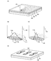
連続発振レーザを半導体膜102に照射すると、連続的に半導体膜102にエネルギーが与えられるため、一旦半導体膜を溶融状態にすると、その状態を継続させることができる。図1(B)においては、レーザビーム105が照射されている半導体膜107は溶融している。さらに、連続発振レーザを走査することによって半導体膜の固液界面を移動させ、ラテラル成長する。即ち、この移動の方向に沿って一方向に長く、幅が0.5μm以上10μm以下、好ましくは1μm以上5μm以下の結晶粒を形成することができる。図2(A)は、図1(B)の斜視図であり、図2(B)は、図2(A)のレーザビーム105の照射領域の拡大図、及びレーザビームのビームスポット110の長さ方向110aのエネルギー分布112aを示し、図2(C)はレーザビームのビームスポット110の幅方向110bのエネルギー分布112bを示す。レーザビームが走査された半導体膜は、ビームスポット110からレーザ走査方向に伸びた結晶粒113が形成されその幅は0.5μm以上10μm以下、好ましくは1μm以上5μm以下である。
When the
その際に固体レーザを用いるのは、気体レーザ等と比較して、出力の安定性が高く、安定した処理が見込まれるためである。なお、連続発振レーザに限らず、繰り返し周波数が10MHz以上のパルスレーザを用いることも可能である。 The solid laser is used at that time because the output stability is higher than that of a gas laser or the like and stable processing is expected. Note that not only a continuous wave laser but also a pulse laser having a repetition frequency of 10 MHz or more can be used.
その際に繰り返し周波数が高いパルスレーザを用いると、半導体膜が溶融してから固化するまでの時間よりもレーザのパルス間隔が短ければ、常に半導体膜を膜厚方向全体において溶融状態にとどめることができ、固液界面の移動により一方向に長い結晶粒で構成される半導体膜を形成することができる。この場合は、例外的にレーザのパルス幅が半導体膜の溶融時間より極めて小さくなるが、レーザの性質としては連続発振レーザとほぼ同等なので、連続発振レーザと同様の扱いができる。なお、図7の場合ではレーザ発振器を2台用意したが、出力が十分であれば1台でよい。 In this case, if a pulse laser having a high repetition frequency is used, the semiconductor film can always be kept in a molten state in the entire film thickness direction if the pulse interval of the laser is shorter than the time from the melting of the semiconductor film to solidification. In addition, a semiconductor film composed of crystal grains that are long in one direction can be formed by moving the solid-liquid interface. In this case, the pulse width of the laser is exceptionally much smaller than the melting time of the semiconductor film. However, since the laser is almost the same as a continuous wave laser, it can be handled in the same way as a continuous wave laser. In the case of FIG. 7, two laser oscillators are prepared. However, if the output is sufficient, one laser oscillator may be used.
本実施の形態では、レーザ発振器11a、11bにNd:YVO4レーザを用いたが、繰り返し周波数が10MHz以上のパルスレーザや、その他の連続発振レーザを使用することもできる。例えば、気体レーザとしては、Arレーザ、Krレーザ、CO2レーザ等がある。固体レーザとして、YAGレーザ、YLFレーザ、YAlO3レーザ、GdVO4レーザ、KGWレーザ、KYWレーザ、アレキサンドライトレーザ、Ti:サファイアレーザ、Y2O3レーザ、Nd:YVO4レーザ等がある。さらに、YAGレーザ、Y2O3レーザ、GdVO4レーザ、Nd:YVO4レーザ等のセラミックスレーザがある。また、金属蒸気レーザとしてはヘリウムカドミウムレーザ等が挙げられる。
In this embodiment, the Nd: YVO 4 laser is used for the
また、レーザ発振器11a、11bとしては、レーザビームをTEM00(シングル横モード)で発振して射出することもでき、このようにすると被照射面において得られる線状ビームスポットの集光性を高め、エネルギー密度を高めることができるので好ましい。
In addition, the
これらのレーザ発振器を用いて射出されたレーザの光学的処理の概要は以下の通りである。レーザ発振器11a、11bからレーザビーム12a、12bをそれぞれ同じエネルギーで射出する。レーザ発振器11bから射出されたレーザビーム12bは、波長板13を通して偏光方向を変えるが、それは偏光子14によって互いに偏光方向が異なる2つのレーザビームを合成するためである。
The outline of the optical processing of the laser emitted using these laser oscillators is as follows.
その波長板13にレーザビーム12bを通した後、ミラー22で反射させ、偏光子14にレーザビーム12bを入射させ、その偏光子14でレーザビーム12aとレーザビーム12bを合成し、レーザビーム12とする。その際には波長板13及び偏光子14を透過した光が適当なエネルギーとなるように波長板13と偏光子14を調整する。なお、本実施の形態では、レーザビームの合成に偏光子14を用いているが、偏光ビームスプリッターなどの他の光学素子を用いてもよい。
After passing the
その偏光子14によって合成されたレーザビーム12は、ミラー15によって反射され、焦点距離が、例えば150mmのシリンドリカルレンズ16及び焦点距離が、例えば20mmのシリンドリカルレンズ17によって、レーザビームの断面形状を被照射面18において線状に整形する。なお、ミラー15はレーザ照射装置の光学系の設置状況に応じて設ければよい。
The
その際には、シリンドリカルレンズ16は被照射面18で形成されるビームスポットの長さ方向に作用し、シリンドリカルレンズ17はその幅方向に作用するものであり、これらにより、被照射面18において、例えば長さ500μm、幅20μm程度の線状のビームスポットが形成される。なお、本実施の形態では、線状に成形するためにシリンドリカルレンズを用いているが、これには限らず、球面レンズ、シリンドリカルレンズアレイ、回折光学素子、光導波路などのその他の光学素子を用いてもよいし、シリンドリカルレンズの焦点距離は上記の値に限らず、自由に設定することができる。
In that case, the
本発明では、前記したとおりセラミックレーザを用いることができ、それを用いた場合には、レーザの媒質の形状を比較的自由に整形することが可能であるため、そのようなレーザビームの作製に適している。なお、線状に形成されたレーザビームの断面形状は出来るだけ幅が細い方が好ましく、これにより半導体膜におけるレーザビームのエネルギー密度が上がるため、工程時間を短縮できる。 In the present invention, a ceramic laser can be used as described above, and when it is used, the shape of the laser medium can be shaped relatively freely. Is suitable. Note that the cross-sectional shape of the laser beam formed in a linear shape is preferably as narrow as possible. This increases the energy density of the laser beam in the semiconductor film, so that the process time can be shortened.
次に、レーザビームの照射方法について説明する。キャップ膜103に覆われた半導体膜102が形成された被照射面18を比較的高速で動作させるため、吸着ステージ19に固定する。吸着ステージ19は、X軸用の一軸ロボット20とY軸用の一軸ロボット21により、被照射面18に平行な面上をXY方向に動作でき、線状のビームスポットの長さ方向とY軸を一致させて配置する。
Next, a laser beam irradiation method will be described. The
それに続いて、ビームスポットの幅方向、つまりX軸に沿って被照射面18を動作させ、レーザビームを被照射面18に照射する。ここでは、X軸用の一軸ロボット20の走査速度を35cm/sec、また2台のレーザ発振器からそれぞれ7.0Wのエネルギーでレーザを射出しており、合成後のレーザの出力は14Wとなる。そのレーザビームが照射されることによって半導体が完全溶融した領域が形成され、固化される過程で結晶粒の幅が0.5μm以上10μm以下、好ましくは1μm以上5μm以下である結晶粒を有する結晶性半導体膜、さらにはひとつの面方位に結晶が成長し、本発明の結晶性半導体膜を形成することができる。
Subsequently, the
また、X軸用の一軸ロボット20の走査速度は、数cm/s〜数100cm/sec程度が適当であり、レーザ発振器の出力に合わせて作業者が適宜決定すればよい。
The scanning speed of the
なお、本実施の形態では、X軸用の一軸ロボット20およびY軸用の一軸ロボット21を用いて、被照射面18を有する基板100を移動させる方式を用いているが、これに限らず、レーザビームの走査は、被照射面18を固定してレーザビームの照射位置を移動させる照射系移動型、レーザビームの照射位置を固定して被照射面18を移動させる被照射面移動型、または上記2つの方法を組み合わせた方法も用いることができる。
In the present embodiment, a method of moving the
さらに、上述したように、上記した光学系によって形成されるビームスポットの長さ方向のエネルギー分布はガウス分布であるため、その両端のエネルギー密度の低い箇所では小粒径結晶が形成される。そこで、結晶粒の幅を0.5μm以上10μm以下、好ましくは1μm以上5μm以下に制御するのに充分なエネルギーのみが被照射面18に照射されるよう、被照射面18の手前にスリット等を設けレーザビームの一部を切り取る構成としてもよい。また、ビームスポットの長さ方向のエネルギー分布において、半導体膜を溶融することが可能なエネルギー分布の領域を重ね合わせながらレーザビームを照射することで、小粒径結晶が形成されるのを回避することができる。
Furthermore, as described above, since the energy distribution in the length direction of the beam spot formed by the above-described optical system is a Gaussian distribution, small grain crystals are formed at locations where the energy density is low at both ends. Therefore, a slit or the like is provided in front of the
また、レーザ発振器11a及び11bから射出されるレーザビームをより効率的に使用するために、レンズアレイや回折光学素子等のビームホモジナイザを用いて、ビームスポットの長さ方向のエネルギーを一様な分布としてもよい。さらに、形成された結晶性半導体膜の幅の分だけ、Y軸用の一軸ロボット21を移動させ、再度X軸用の一軸ロボット20を所定の速度、ここでは35cm/secで走査させることもでき、このような一連の動作を繰り返すことにより、半導体膜全面を効率よく結晶化することができる(図1(C))。
Further, in order to use the laser beams emitted from the
次いで、エッチングを行うことによってキャップ膜を除去し、その後結晶性半導体膜の半導体膜上にレジストを塗布し、レジストを露光し、現像することによって所望の形状にレジストを形成する。さらに、ここで形成したレジストをマスクとしてエッチングを行い、現像によって露出した結晶性半導体膜を除去する。この工程によって、図2(D)に示すように、絶縁膜101上に島状の半導体膜121を形成する。また、この島状の半導体膜を用いて薄膜トランジスタ、ダイオード、抵抗素子、容量素子、CCD等の半導体素子を有する半導体装置を作製することができる。ここでは、図1(D)に示すように、一形態として薄膜トランジスタ150を作製する。
Next, the cap film is removed by etching, and then a resist is applied on the semiconductor film of the crystalline semiconductor film, and the resist is exposed and developed to form a resist in a desired shape. Further, etching is performed using the resist formed here as a mask, and the crystalline semiconductor film exposed by development is removed. Through this step, an island-shaped
次に、本実施の形態で作製した結晶性半導体膜の面方位について述べる。 Next, the plane orientation of the crystalline semiconductor film manufactured in this embodiment will be described.
本実施の形態では、エッチングを行うことによってキャップ膜を除去した結晶性半導体膜の、結晶粒の位置と大きさ、および結晶の面方位について、EBSP(Electron Back Scatter Diffraction Pattern;電子後方散乱回折像)測定を行っており、まずEBSPの基本的事項を説明し、ついで補足的説明を加えながら結果について説明する。 In this embodiment mode, an EBSP (Electron Back Scatter Diffraction Pattern: electron backscatter diffraction image) is used for the position and size of crystal grains and the crystal plane orientation of the crystalline semiconductor film from which the cap film has been removed by etching. ) We are measuring, first we will explain the basics of EBSP, then we will explain the results with additional explanations.
そのEBSPとは、走査型電子顕微鏡(SEM:Scanning Electron Microscopy)にEBSP検出器を接続し、走査型電子顕微鏡内で高傾斜した試料に収束電子ビームを照射したときに発生する個々の結晶の回折像(EBSP像)の方位を解析し、方位データと測定点の位置情報(x,y)から試料の結晶の面方位を測定する方法である。 The EBSP refers to diffraction of individual crystals generated when a EBSP detector is connected to a scanning electron microscope (SEM) and a focused electron beam is irradiated to a highly inclined sample in the scanning electron microscope. In this method, the orientation of the image (EBSP image) is analyzed, and the crystal orientation of the sample crystal is measured from the orientation data and position information (x, y) of the measurement point.
結晶性半導体膜に電子線を入射させると、後方にも非弾性散乱が起こり、その中には試料中でブラッグ回折による結晶の面方位に特有な線状のパターンも合わせて観察することができる。ここで、この線状のパターンは一般的に菊池線と呼ばれており、EBSP法は、検出器に映った菊池線を解析することによって結晶性半導体膜の結晶の面方位を求めるものである。 When an electron beam is incident on a crystalline semiconductor film, inelastic scattering occurs also in the back, and a linear pattern peculiar to the crystal plane orientation by Bragg diffraction can also be observed in the sample. . Here, this linear pattern is generally called a Kikuchi line, and the EBSP method obtains the crystal orientation of the crystalline semiconductor film by analyzing the Kikuchi line reflected in the detector. .
多結晶構造の試料は、各結晶粒が異なった面方位を持っている。そこで、結晶性半導体膜の照射位置を移動させる度に電子線を照射し、照射位置ごとに結晶の面方位の解析を行う。このようにして、平坦な表面を持つ結晶性半導体膜の結晶の面方位や配向情報を得ることができ、測定領域が広いほど結晶性半導体膜全体の面方位の傾向を得ることがでるので、測定点が多いほど測定領域中の結晶の面方位の情報を詳細に得ることができる。 In a sample having a polycrystalline structure, each crystal grain has a different plane orientation. Therefore, the electron beam is irradiated every time the irradiation position of the crystalline semiconductor film is moved, and the crystal plane orientation is analyzed for each irradiation position. In this way, the crystal plane orientation and orientation information of the crystalline semiconductor film having a flat surface can be obtained, and the tendency of the plane orientation of the entire crystalline semiconductor film can be obtained as the measurement region is wide. As the number of measurement points increases, information on the crystal plane orientation in the measurement region can be obtained in detail.
しかし、結晶内部の面方位は、結晶の一つの観察面からの測定による面方位のみで決定することはできない。それは、一観察面のみにおいて面方位が一方向に揃っていたとしても、他の観察面において面方位が揃っていなければ、その結晶内部の面方位が揃っているとは言えないからであり、そのため、結晶内部の面方位を決定するには、少なくとも二つの表面からの面方位が必要となり、より多くの面からの情報が多くなるほど精度が高くなる。 However, the plane orientation inside the crystal cannot be determined only by the plane orientation measured from one observation plane of the crystal. That is because even if the plane orientation is aligned in one direction only on one observation plane, if the plane orientation is not aligned on the other observation plane, it cannot be said that the plane orientation inside the crystal is aligned, Therefore, in order to determine the plane orientation inside the crystal, plane orientations from at least two surfaces are required, and the accuracy increases as the information from more planes increases.
測定領域内で3つの面とも面方位分布が均一であれば、近似的に単一の結晶と見なすことができる。実際には、図3に示すように、互いに直交する3つのベクトル(ベクトルa、ベクトルb、ベクトルc)がそれぞれ法線ベクトルとなる3つの面(観察面A、観察面B、観察面C)の情報を総合することによって、高精度で結晶内部の面方位を特定することができる。 If the plane orientation distribution is uniform on all three surfaces in the measurement region, it can be regarded approximately as a single crystal. Actually, as shown in FIG. 3, three planes (observation plane A, observation plane B, observation plane C) in which three vectors orthogonal to each other (vector a, vector b, vector c) are normal vectors, respectively. By combining the above information, the plane orientation inside the crystal can be specified with high accuracy.
本実施の形態において形成される結晶性半導体膜では、以下のようにベクトルa〜cを設定した。ベクトルcはレーザビームの走査方向(即ち、結晶粒の成長方向)及び基板表面と平行であり、ベクトルaは基板表面及びベクトルcと垂直であり、ベクトルbは基板の表面に平行であり、かつ結晶粒の結晶成長方向に垂直な方向であって、即ちベクトルa及びベクトルcと互いに垂直である。これら3つの観察面A〜Cからの情報より、結晶膜の面方位を高精度に特定することができる。 In the crystalline semiconductor film formed in the present embodiment, vectors a to c are set as follows. Vector c is parallel to the scanning direction of the laser beam (ie, the growth direction of the grains) and the substrate surface, vector a is perpendicular to the substrate surface and vector c, vector b is parallel to the surface of the substrate, and The direction is perpendicular to the crystal growth direction of the crystal grains, that is, perpendicular to the vectors a and c. From the information from these three observation planes A to C, the plane orientation of the crystal film can be specified with high accuracy.
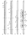
まず、結晶性半導体膜の面方位(観察面に垂直な方向の結晶軸方位)を解析した結果を図4〜図6に示す。本実施の形態において形成される結晶性半導体膜の表面に対し、60°の入射角で電子線を入射し、得られるEBSP像から結晶の面方位を測定した。その測定範囲は、50μm×50μmであり、この領域において、縦横0.1μm毎の格子点状に測定を行った。また、EBSP法の測定面は試料表面であるため、結晶性半導体膜を最上層とする必要があり、そのためキャップ膜である酸素を含む窒化珪素膜をエッチングした後に測定を行った。 First, the results of analyzing the plane orientation of the crystalline semiconductor film (the crystal axis orientation in the direction perpendicular to the observation plane) are shown in FIGS. An electron beam was incident on the surface of the crystalline semiconductor film formed in this embodiment at an incident angle of 60 °, and the crystal plane orientation was measured from the obtained EBSP image. The measurement range is 50 μm × 50 μm, and in this region, measurement was performed in the form of lattice points every 0.1 μm in length and width. In addition, since the measurement surface of the EBSP method is the sample surface, the crystalline semiconductor film needs to be the uppermost layer. Therefore, the measurement was performed after etching the silicon nitride film containing oxygen as the cap film.
ベクトルaが法線ベクトルとなる観察面Aにおける面方位分布を図4(a)に、同様にベクトルbが法線ベクトルとなる観察面Bにおける面方位分布を図4(b)に、ベクトルcが法線ベクトルとなる観察面Cにおける面方位分布を図4(c)に示す。図4(a)〜(c)は、各測定点がどの面方位かを示す方位マップ像で、図4(d)は、結晶の各面方位をカラーコード化して表した図であり、図4(a)〜(c)の測定点の面方位は、図4(d)の面方位に対応する色で示している。 FIG. 4A shows a plane orientation distribution on the observation plane A where the vector a is a normal vector, and FIG. 4B shows a plane orientation distribution on the observation plane B where the vector b is a normal vector. FIG. 4C shows a plane orientation distribution on the observation plane C where is a normal vector. 4A to 4C are orientation map images showing which plane orientation each measurement point has, and FIG. 4D is a diagram in which each plane orientation of the crystal is color-coded. The plane orientations of the measurement points 4 (a) to 4 (c) are indicated by colors corresponding to the plane orientation of FIG. 4 (d).
なお、図4が白黒のため明度のみの表示となっていて判別が難しいが、カラー表示では、観察面Aでは<001>方位に強く配向し、観察面Bでは<301>方位に強く配向し、観察面Cでは<301>方位に強く配向していることが分かる。また、個々の結晶粒の内部は面方位が均一であるため、色と形状によって個々の結晶粒の形状や大きさなどの大まかな情報をつかむことができる。さらに、面方位<401>や<501>、<601>は、面方位<301>と近いため、<301>と概略同じである。 4 is black and white, so it is difficult to discriminate it. However, in color display, the observation plane A is strongly oriented in the <001> direction and the observation plane B is strongly oriented in the <301> direction. It can be seen that the observation plane C is strongly oriented in the <301> direction. In addition, since the inside of each crystal grain has a uniform plane orientation, rough information such as the shape and size of each crystal grain can be grasped by the color and shape. Furthermore, the plane orientation <401>, <501>, and <601> are substantially the same as <301> because they are close to the plane orientation <301>.
ここで、図4(a)〜(c)より、本実施の形態において形成される結晶性半導体膜の結晶粒は、幅が1μm以上5μmで長く伸びたドメインを有することが分かり、図4(a)〜(c)においては、ドメインの長さは5〜50μmであり、さらには、50μm以上の長さのドメインも見られた。なお、図4の測定領域は50μm×50μmであるが、より広い範囲では長さが5〜100μmのドメインも見られる。また、図4(a)〜(c)より、本実施の形態において形成される結晶性半導体膜は、観察面A、B、Cにおいてそれぞれ<001>方位、<301>方位、および<301>方位に強く配向していることが分かる。特定の指数に強く配向していることが分かった場合、その指数近傍にどの程度の結晶粒が集まっているか、その割合を求めることで面における配向の度合いを把握することができる。 Here, it can be seen from FIGS. 4A to 4C that the crystal grains of the crystalline semiconductor film formed in this embodiment have domains that are long and have a width of 1 μm to 5 μm. In a) to (c), the domain length was 5 to 50 μm, and a domain having a length of 50 μm or more was also observed. In addition, although the measurement area | region of FIG. 4 is 50 micrometers x 50 micrometers, the domain of 5-100 micrometers in length is also seen in a wider range. 4A to 4C, the crystalline semiconductor film formed in this embodiment has a <001> orientation, a <301> orientation, and a <301> in the observation planes A, B, and C, respectively. It can be seen that they are strongly oriented in the direction. When it is found that the crystal is strongly oriented to a specific index, it is possible to grasp the degree of orientation in the plane by obtaining the ratio of how many crystal grains are gathered in the vicinity of the index.
図5(a)〜(c)は、図4に示す観察面A〜Cにおける面方位の出現度数分布を表す逆極点図であり、また図5(d)は面方位の出現度数を示すスケールである。その図5では白黒のため明度のみの表示となっていて判別が難しいが、黒に近い領域ほど面方位を有する結晶の割合が高いことを示す。図5(a)に示す逆極点図から、観察面Aでは<001>方位ほど黒に近く、具体的には、全ての方位が等しい確率で現れる状態の14.0倍以上の頻度で<001>方位が出現することがわかった。 FIGS. 5A to 5C are reverse pole figures showing the distribution of appearance frequencies of the plane orientations on the observation planes A to C shown in FIG. 4, and FIG. 5D is a scale showing the appearance frequencies of the plane orientations. It is. In FIG. 5, since only the brightness is displayed because it is black and white, it is difficult to discriminate, but the region closer to black shows a higher proportion of crystals having a plane orientation. From the inverted pole figure shown in FIG. 5 (a), the <001> orientation is closer to black on the observation plane A, specifically, <001 at a frequency of 14.0 times or more of the state in which all orientations appear with equal probability. > It was found that the direction appeared.
また、図5(b)に示す逆極点図から、観察面Bでは<301>方位が最も黒に近く、具体的には、全ての方位が等しい確率で現れる状態の4.8倍以上の頻度で<301>方位が出現することがわかった。さらに、図5(c)に示す逆極点図から、観察面Cでは<301>方位が最も黒に近く、具体的には、全ての方位が等しい確率で現れる状態の4.8倍以上の頻度で<301>方位が出現することがわかった。 Further, from the inverted pole figure shown in FIG. 5B, the <301> orientation is closest to black on the observation plane B, and more specifically, the frequency is 4.8 times or more the state where all the orientations appear with the same probability. It turns out that <301> orientation appears. Further, from the inverse pole figure shown in FIG. 5C, the <301> orientation is closest to black on the observation plane C, and more specifically, the frequency is 4.8 times or more that the state in which all orientations appear with the same probability. It turns out that <301> orientation appears.
図5(a)〜(c)の逆極点図において出現頻度が高い面方位について配向率を求め、その配向率の計算結果を図6(a)〜(c)に示す。図6(a)は観察面Aにおける配向率を求めた結果であり、その配向率は図5(a)の逆極点図において、<001>方位の角度揺らぎの範囲を±10°以内と決めて、全ての測定点に対する<001>方位の角度揺らぎが±10°以内に存在する測定点の数の割合を求めることにより求めた。なお、図6(A)において色が塗られた領域は、<001>方位の角度揺らぎが±10°以内である結晶を示す領域である。 In the reverse pole figures of FIGS. 5A to 5C, the orientation rate is obtained for the plane orientation having a high appearance frequency, and the calculation results of the orientation rates are shown in FIGS. 6A to 6C. FIG. 6A shows the result of obtaining the orientation rate on the observation plane A. The orientation rate is determined by setting the range of <001> orientation angle fluctuation within ± 10 ° in the reverse pole figure of FIG. 5A. Thus, the angle fluctuation of the <001> azimuth with respect to all the measurement points was obtained by determining the ratio of the number of measurement points existing within ± 10 °. Note that a colored region in FIG. 6A is a region indicating a crystal whose <001> orientation angle fluctuation is within ± 10 °.
また、全測定点のうち特定の配向を持つ点の比率を求めた値がPartition F
ractionの値であり、全測定点に対してこの特定の配向を持つ点のうち配向付けの信頼性が高い測定点の配向比率を求めた値がTotal Fractionの値である。この結果から、実施の形態において形成される結晶性半導体膜の観察面Aにおいては、±10°の角度揺らぎの範囲内において<001>方位が71.2%を占める。なお、結晶の面方位は[100]、[010]、[001]、さらには前記方位のそれぞれの1が−1である面方位のように等価な方位群をまとめて<001>と表記している。
In addition, a value obtained by calculating a ratio of points having a specific orientation among all measurement points is Partition F.
It is a value of traction, and a value obtained by obtaining an orientation ratio of measurement points having high orientation reliability among points having this specific orientation with respect to all measurement points is a value of Total Fraction. From this result, in the observation surface A of the crystalline semiconductor film formed in the embodiment, the <001> orientation occupies 71.2% within the range of ± 10 ° angular fluctuation. The plane orientation of the crystal is [100], [010], [001], and equivalent orientation groups such as plane orientations in which each 1 of the orientation is −1 are collectively expressed as <001>. ing.
図6(b)、(c)は、図5(b)及び(c)をもとに、図6(a)と同様に観察面B及びCにおける配向率を求めた結果である。なお、図6(b)及び(c)の色が塗られた領域は、<301>方位の角度揺らぎが±10°以内である結晶を示す領域であり、実施の形態において形成される結晶性半導体膜の観察面Bにおいては、±10°の角度揺らぎの範囲内において<301>方位が71.1%を占める。 FIGS. 6B and 6C show the results of obtaining the orientation ratios on the observation surfaces B and C based on FIGS. 5B and 5C in the same manner as FIG. 6A. 6B and 6C is a region showing a crystal having an angle fluctuation of <301> orientation within ± 10 °, and the crystallinity formed in the embodiment In the observation plane B of the semiconductor film, the <301> orientation occupies 71.1% within an angular fluctuation range of ± 10 °.
本実施の形態において形成される結晶性半導体膜の観察面Cにおいては、±10°の角度揺らぎの範囲内において<301>方位が73.9%を占める。なお、結晶の面方位は[310]、[301]、[013]、さらには前記面方位それぞれの1及び3の一方または両方が負の値である面方位のように等価な方位群をまとめて<301>と示している。また、観察面B及びCにおいては、面方位<301>の割合を示したが、面方位<301>と近い面方位<401>や<501>、<601>の配向率の割合としてもよい。
In the observation plane C of the crystalline semiconductor film formed in this embodiment, the <301> orientation occupies 73.9% within the range of ± 10 ° angular fluctuation. The plane orientation of the crystal is [310], [301], [013], and equivalent orientation groups such as plane orientations in which one or both of the
以上に示すように、3つの観察面それぞれにおいて結晶の面方位が一つの方向に高い割合で揃っている。つまり、結晶化された領域において、結晶の面方位が一方向に揃っているとみなすことができる結晶が形成されていることがわかる。このようにして、一辺が数十μmの領域内で、特定の面方位が非常に高い比率を占める結晶がガラス基板上に形成されることが確認された。 As described above, the crystal orientations of the three observation planes are aligned at a high rate in one direction. That is, it can be seen that in the crystallized region, a crystal that can be regarded as having crystal plane orientations aligned in one direction is formed. In this way, it was confirmed that a crystal in which a specific plane orientation occupies a very high ratio is formed on a glass substrate within a region having a side of several tens of μm.
なお、EBSPの測定は、例えば薄膜トランジスタのチャネル領域で測定可能である。即ち、ゲート配線及びゲート絶縁膜で覆われる半導体層で測定可能である。 Note that EBSP can be measured, for example, in the channel region of a thin film transistor. That is, measurement is possible with a semiconductor layer covered with a gate wiring and a gate insulating film.
以上の結果より、本実施の形態で作製した結晶性半導体膜の面方位をEBSPにより測定すると、観察面Aにおいては、±10°の角度揺らぎの範囲内において<001>方位が6割以上9割以下、好ましくは7割以上8割以下である。また、観察面Bにおいては、±10°の角度揺らぎの範囲内において<301>方位が6割以上9割以下、好ましくは7割以上8割以下であり、観察面Cにおいては、±10°の角度揺らぎの範囲内において<301>方位が6割以上9割以下、好ましくは7割以上8割以下である。 From the above results, when the plane orientation of the crystalline semiconductor film manufactured in this embodiment is measured by EBSP, in the observation plane A, the <001> orientation is 60% or more within an angular fluctuation range of ± 10 °. 20% or less, preferably 70% or more and 80% or less. On the observation plane B, the <301> orientation is 60% to 90%, preferably 70% to 80%, within the range of ± 10 ° angular fluctuation, and on the observation plane C, ± 10 °. In the range of the angle fluctuation, the <301> orientation is 60% to 90%, preferably 70% to 80%.
本実施の形態において形成される結晶性半導体膜は、結晶粒の幅が0.5μm以上10μm以下、好ましくは1μm以上5μm以下であり、且つ結晶の面方位が一方向、または実質的に一方向とみなすことができる方向に揃っている。つまり、性質は単結晶に近い半導体膜であり、このような半導体膜を用いると、半導体装置の性能を大幅に向上させることが可能である。例えば、この結晶性半導体膜を用いてTFTを形成した場合、単結晶半導体を用いた半導体装置と同等の電界効果移動度(モビリティ)を得ることが可能である。 The crystalline semiconductor film formed in this embodiment has a crystal grain width of 0.5 μm to 10 μm, preferably 1 μm to 5 μm, and a crystal plane orientation in one direction or substantially in one direction. It is aligned in the direction that can be regarded as. That is, the property is a semiconductor film close to a single crystal, and the use of such a semiconductor film can greatly improve the performance of the semiconductor device. For example, when a TFT is formed using this crystalline semiconductor film, field-effect mobility (mobility) equivalent to that of a semiconductor device using a single crystal semiconductor can be obtained.
また、そのTFTでは、オン電流値(TFTがオンの状態にあるときに流れるドレイン電流の値)、オフ電流値(TFTがオフの状態にあるときに流れるドレイン電流の値)、しきい値電圧、S値および電界効果移動度のばらつきを低減させることが可能になる。このような効果があるため、TFTの電気的特性は向上し、そのTFTを用いた半導体装置の動作特性および信頼性が向上する。 従って、高速動作が可能で電流駆動能力が高く、複数の素子間において性能のばらつきが小さい半導体装置を製作することができる。 In addition, in the TFT, an on-current value (a drain current value that flows when the TFT is in an on state), an off-current value (a drain current value that flows when the TFT is in an off state), a threshold voltage , Variation in S value and field effect mobility can be reduced. Because of such effects, the electrical characteristics of the TFT are improved, and the operating characteristics and reliability of the semiconductor device using the TFT are improved. Therefore, it is possible to manufacture a semiconductor device that can operate at high speed, has high current driving capability, and has small performance variation among a plurality of elements.
(実施の形態2)
本実施の形態では、半導体装置の一例である液晶表示装置について図9、及び図10を用いて説明する。
(Embodiment 2)
In this embodiment, a liquid crystal display device which is an example of a semiconductor device will be described with reference to FIGS.
図9(A)に示すように、実施の形態1と同様に基板100上に下地膜として機能する絶縁膜101を形成し、絶縁膜101上に半導体膜102を形成し、半導体膜102上にキャップ膜103を形成する。
As shown in FIG. 9A, an insulating
ここでは、基板100として、ガラス基板を用い、絶縁膜101としては、厚さ40〜60nmの酸素を含む窒化珪素膜及び厚さ80〜120nmの窒素を含む酸化珪素膜をそれぞれプラズマCVD法により形成する。また、半導体膜102としてプラズマCVD法により厚さ20〜80nmの非晶質半導体膜を形成し、キャップ膜103としては、プラズマCVD法により厚さ200nm以上1000nm以下の酸素を0.1〜10atomic%含み、かつ珪素に対する窒素の組成比が1.3以上1.5以下である窒化珪素膜を形成する。
Here, a glass substrate is used as the
次に、基板100を加熱する。ここでは、基板100上に形成された非晶質半導体膜の水素を除去するための加熱を行う。ここでは、基板100を500℃で1時間加熱した後、550℃で4時間加熱する。
Next, the
次に、図9(B)に示すように、キャップ膜103にレーザビーム105を照射したのち、キャップ膜103を除去する。このときのレーザビーム105は、半導体膜102を溶融することが可能なエネルギーを選択する。また、半導体膜102が吸収することが可能なレーザビーム105の波長を選択する。この結果、絶縁膜101上に結晶性半導体膜106を形成することができる。ここでは、レーザビーム105としてNd:YVO4の第2高調波を用い、その後、キャップ膜103を除去する。キャップ膜103の除去方法としては、ドライエッチング、ウエットエッチング、研磨等の各種除去方法を用いることができるが、ここでは、ドライエッチング法によりキャップ膜103を除去する。
Next, as shown in FIG. 9B, after the
次に、図9(C)に示すように結晶性半導体膜106を選択的にエッチングして半導体膜201〜203を形成する。ここでは、結晶性半導体膜106のエッチング方法としては、ドライエッチング、ウエットエッチング等を用いることができる。ここでは、結晶性半導体膜106上にレジストを塗布した後、露光及び現像を行ってレジストマスクを形成する。次に、レジストマスクを用いてSF6:O2の流量比を4:15としたドライエッチング法により、結晶性半導体膜106を選択的にエッチングする。この後、レジストマスクを除去する。
Next, as illustrated in FIG. 9C, the
次に、図9(D)に示すように、半導体膜201〜203上にゲート絶縁膜204を形成する。ゲート絶縁膜は、窒化珪素、酸素を含む窒化珪素、酸化珪素、窒素を含む酸化珪素等の単層又は積層構造で形成する。ここでは、厚さ115nmの窒素を含む酸化珪素をプラズマCVD法により形成する。
Next, as illustrated in FIG. 9D, the
次にゲート電極205〜208を形成する。ゲート電極205〜208は、金属又は一導電型の不純物を添加した多結晶半導体で形成することができる。金属を用いる場合は、タングステン、モリブデン、チタン、タンタル、アルミニウムなどを用いることができる。また、金属を窒化させた金属窒化物を用いることができる。或いは、当該金属窒化物からなる第1の層と当該金属から成る第2の層とを積層させた構造としても良い。また、液滴吐出法を用いて微粒子を含むペーストをゲート絶縁膜上に吐出し、乾燥・焼成して形成することができる。また、ゲート絶縁膜上に、微粒子を含むペーストを印刷法により印刷し、乾燥・焼成して形成することができる。微粒子の代表例としては、金、銀、銅、金と銀の合金、金と銅の合金、銀と銅の合金、金と銀と銅の合金のいずれかを主成分とする微粒子でもよい。ここでは、ゲート絶縁膜204上に、膜厚30nmmの窒化タンタル膜及び、膜厚370nmのタングステン膜をスパッタリング法により形成した後、フォトリソグラフィー工程により形成したレジストマスクを用いて窒化タンタル膜、及びタングステン膜を選択的にエッチングして、窒化タンタル膜の端部がタングステン膜の端部より外側に突き出した形状のゲート電極205〜208を形成する。
Next,
次に、ゲート電極205〜208をマスクとして、半導体膜201〜203にそれぞれn型を付与する不純物元素及びp型を付与する不純物元素を添加して、ソース領域及びドレイン領域209〜214及び高濃度不純物領域215を形成する。また、ゲート電極205〜208の一部に重複する低濃度不純物領域216〜223を形成する。さらに、ゲート電極205〜208と重複するチャネル領域201c〜203c、203dを形成する。ここでは、ソース領域及びドレイン領域209、210、213〜214、高濃度不純物領域215、及び低濃度不純物領域216、217、220〜223に、p型を付与する不純物元素であるボロンをドーピングする。また、ソース領域及びドレイン領域211、212、及び低濃度不純物領域218、219に、n型を付与する不純物元素であるリンをドーピングする。
Next, an impurity element imparting n-type conductivity and an impurity element imparting p-type conductivity are added to the
この後、半導体膜に添加した不純物元素を活性化するために加熱処理を行う。ここでは、窒素雰囲気で550度4時間の加熱を行う。以上の工程により、薄膜トランジスタ225〜227を形成する。なお、薄膜トランジスタ225、227としてはpチャネル型の薄膜トランジスタを形成し、薄膜トランジスタ226としてはnチャネル型の薄膜トランジスタを形成する。また、pチャネル型の薄膜トランジスタ225及びnチャネル型の薄膜トランジスタ226により駆動回路を構成する。また、pチャネル型の薄膜トランジスタ227は、画素の電極に電圧を印加する素子として機能する。
Thereafter, heat treatment is performed to activate the impurity element added to the semiconductor film. Here, heating is performed at 550 ° C. for 4 hours in a nitrogen atmosphere. Through the above steps,
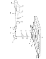
次に、図10(A)に示すように、薄膜トランジスタ225〜227のゲート電極及び配線を絶縁化する第1の層間絶縁膜を形成する。ここでは、第1の層間絶縁膜として酸化珪素膜231、窒化珪素膜232、及び酸化珪素膜233を積層して形成する。また、第1の層間絶縁膜の一部である酸化珪素膜233上に薄膜トランジスタ225〜227のソース領域及びドレイン領域に接続する配線234〜239、及び接続端子240を形成する。ここでは、スパッタリング法により、Ti膜100nm、Al膜300nm、Ti膜100nmを連続した後、フォトリソグラフィー工程によって形成したレジストマスクを用いて選択的にエッチングして、配線234〜239、及び接続端子240を形成する。その後、レジストマスクを除去する。
Next, as shown in FIG. 10A, a first interlayer insulating film for insulating the gate electrodes and wirings of the
次いで、第1の層間絶縁膜、配線234〜239、及び接続端子240上に、第2の層間絶縁膜241を形成する。第2の層間絶縁膜241としては、酸化珪素膜、窒化珪素膜または窒素を含む酸化珪素膜などの無機絶縁膜を用いることができ、これらの絶縁膜を単層又は2以上の複数層で形成すればよい。また、無機絶縁膜を形成する方法としてはスパッタ法、LPCVD法、またはプラズマCVD法等を用いればよい。ここでは、プラズマCVD法を用い、膜厚100nm〜150nmの酸素を含む窒化珪素膜を形成した後、フォトリソグラフィー工程により形成したレジストマスクを用いて酸素を含む窒化珪素膜を選択的にエッチングして、薄膜トランジスタ227の配線239、及び接続端子240に達するコンタクトホールを形成するとともに、第2の層間絶縁膜241を形成する。その後、レジストマスクを除去する。
Next, a second
本実施の形態のように、第2の層間絶縁膜241を形成することで、駆動回路部のTFTや配線等の露出を防ぎ、汚染物質からTFTを保護することができる。
By forming the second
次に、薄膜トランジスタ227の配線239に接続する第1の画素電極242、及び接続端子240と接続する導電膜244を形成する。液晶表示装置が透光型液晶表示装置の場合は、第1の画素電極242を透光性を有する導電膜で形成する。また、液晶表示装置が反射型液晶表示装置の場合は、第1の画素電極242を反射性を有する導電膜で形成する。ここでは、第1の画素電極242及び導電膜244は、スパッタリング法により膜厚125nmの酸化珪素を含むITOを成膜した後、フォトリソグラフィー工程により形成したレジストマスクを用いて選択的にエッチングして形成する。
Next, a
次に、配向膜として機能する絶縁膜243を形成する。絶縁膜243は、ポリイミドやポリビニルアルコール等の高分子化合物膜を印刷法、ロールコート法、印刷法等で形成した後、ラビングすることにより形成することができる。また、SiOを基板に対して斜めから蒸着して形成することができる。また、光反応型の高分子化合物に偏光したUV光を照射し光反応型の高分子化合物を重合させて形成することができる。ここでは、ポリイミドやポリビニルアルコール等の高分子化合物膜を印刷法により印刷し、焼成した後、ラビングすることで形成する。
Next, an insulating
次に、図10(B)に示すように、対向基板251に第2の画素電極253を形成し、第2の画素電極上に配向膜として機能する絶縁膜254を形成する。なお、対向基板251及び画素電極253の間に着色膜252を設けても良い。
Next, as illustrated in FIG. 10B, a
対向基板251としては、基板100と同様のものを適宜選択することができる。また、第2の画素電極253は第1の画素電極242と同様に形成することができる。また、配向膜として機能する絶縁膜254は、絶縁膜243と同様に形成することができる。着色膜252としては、カラー表示を行う場合に必要な膜であり、RGB方式の場合は、赤、緑、青の各色に対応した染料や顔料が分散された着色膜を各画素に対応して形成する。
As the
次に、基板100及び対向基板251をシール材257で貼り合わせる。また、基板100及び対向基板251の間に液晶層255を形成する。また、液晶層255は、毛細管現象を利用した真空注入法により、配向膜として機能する絶縁膜243、254、及びシール材257で囲まれた領域に液晶材料を注入することにより形成することができる。また、対向基板251の一方にシール材157を形成し、シール材に囲まれる領域に液晶材料を滴下した後、対向基板251及び基板100を減圧下においてシール材で圧着することで液晶層255を形成することができる。
Next, the
シール材257としては、熱硬化型のエポキシ樹脂、UV硬化型のアクリル樹脂、熱可塑方のナイロン、ポリエステル等を、ディスペンサ法、印刷法、熱圧着法等を用いて形成することができる。なお、シール材257にフィラーを散布することにより、基板100及び対向基板251の間隔を保つことができる。ここでは、シール材257として熱硬化型のエポキシ樹脂を用いて形成する。
As the
また、基板100及び対向基板251の間隔を保つために、配向膜として機能する絶縁膜243、254の間にスペーサ256を設けてもよい。スペーサとしては、有機樹脂を塗布し、該有機樹脂を所望の形状、代表的には柱状又は円柱状にエッチングして形成することができる。また、スペーサとしてビーズスペーサを用いてもよい。ここでは、スペーサ256としてビーズスペーサを用いる。
Further, a
また、図示しないが、基板100、対向基板251の一方又は両方に偏光板を設ける。
Although not illustrated, a polarizing plate is provided on one or both of the
次に、図10(C)に示すように、端子部263においては、薄膜トランジスタのゲート配線、ソース配線に接続される接続端子(図10(C)においては、ソース配線またはドレイン配線に接続される接続端子240を示す。)が形成されている。接続端子240に、導電膜244及び異方性導電膜261を介して入力端子となるFPC(フレキシブルプリント配線)262を接続する。接続端子240は導電膜244及び異方性導電膜261を介してビデオ信号やクロック信号を受け取る。
Next, as illustrated in FIG. 10C, in the
駆動回路部264においては、ソースドライバやゲートドライバ等の画素を駆動する回路が形成される。ここでは、nチャネル型の薄膜トランジスタ226、pチャネル型の薄膜トランジスタ225が配置されている。なお、nチャネル型の薄膜トランジスタ226及びpチャネル型の薄膜トランジスタ225によりCMOS回路が形成されている。
In the
画素部265には、複数の画素が形成されており、各画素には液晶素子258が形成されている。液晶素子258は、第1の画素電極242、第2の画素電極253及びその間に充填されている液晶層255が重なっている部分である。液晶素子258が有する第1の画素電極242は、薄膜トランジスタ227と電気的に接続されている。
A plurality of pixels are formed in the
以上の工程により液晶表示装置を作製することができ、本実施の形態で示す液晶表示装置は、駆動回路部264や画素部265に形成される薄膜トランジスタの半導体層において、結晶粒の幅を0.5μm以上10μm以下、好ましくは1μm以上5μm以下とし、さらには結晶の面方位が一定方向に揃えることができる。このため、複数の薄膜トランジスタの電気特性のばらつきを抑えることが可能であり、その結果、色むらや欠陥の少ない高精細な表示が可能な液晶表示装置を作製することができる。
Through the above process, a liquid crystal display device can be manufactured. In the liquid crystal display device described in this embodiment, the width of crystal grains in the semiconductor layer of the thin film transistor formed in the
(実施の形態3)
本実施の形態では、半導体装置の一例である発光素子を有する発光装置の作製工程について説明する。
(Embodiment 3)
In this embodiment, a manufacturing process of a light-emitting device having a light-emitting element which is an example of a semiconductor device will be described.
図11(A)に示すように、実施の形態2と同様の工程により、基板100上に絶縁膜101を介して薄膜トランジスタ225〜227を形成する。また、薄膜トランジスタ225〜227のゲート電極及び配線を絶縁化する第1の層間絶縁膜として、酸化珪素膜231、窒化珪素膜232、及び酸化珪素膜233を積層して形成する。また、第1の層間絶縁膜の一部の酸化珪素膜233上に薄膜トランジスタ225〜227の半導体膜に接続する配線308〜313、及び接続端子314を形成する。
As shown in FIG. 11A,
次に、第1の層間絶縁膜、配線308〜313、及び接続端子314上に、第2の層間絶縁膜315を形成する。次に、薄膜トランジスタ227の配線313に接続する第1の電極316、及び接続端子314と接続する導電膜320を形成する。第1の電極316及び導電膜320は、スパッタリング法により膜厚125nmの酸化珪素を含むITOを成膜した後、フォトリソグラフィー工程により形成したレジストマスクを用いて選択的にエッチングして形成する。
Next, a second
本実施の形態のように、第2の層間絶縁膜315を形成することで、駆動回路部のTFTや配線等の露出を防ぎ、汚染物質からTFTを保護することができる。
By forming the second
次に、第1の電極316の端部を覆う有機絶縁物膜317を形成する。ここでは、感光性ポリイミドを塗布し焼成した後、露光及び現像を行って駆動回路、画素領域の第1の電極316、及び画素領域の周辺部における第2の層間絶縁膜315が露出されるように有機絶縁物膜317を形成する。
Next, an organic
次に、第1の電極316及び有機絶縁物膜317の一部上に蒸着法により発光物質を含む層318を形成する。発光物質を含む層318は、発光性を有する有機化合物、または発光性を有する無機化合物で形成する。また、発光物質を含む層318を、発光性を有する有機化合物及び発光性を有する無機化合物で形成してもよい。また、発光物質を含む層318を赤色の発光性の発光物質、青色の発光性の発光物質、及び緑色の発光性の発光物質を用いて、それぞれ赤色の発光性の画素、青色の発光性の画素、及び緑色の発光性の画素を形成することができる。
Next, a
ここでは、赤色の発光性の発光物質を含む層として、DNTPDを50nm、NPBを10nm、ビス[2,3−ビス(4−フルオロフェニル)キノキサリナト]イリジウム(アセチルアセトナート)(略称:Ir(Fdpq)2(acac))が添加されたNPBを30nm、Alq3を60nm、及びLiFを1nm積層して形成する。 Here, as a layer containing a red light-emitting substance, DNTPD is 50 nm, NPB is 10 nm, bis [2,3-bis (4-fluorophenyl) quinoxalinato] iridium (acetylacetonate) (abbreviation: Ir (Fdpq ) 2 (acac)) is added to 30 nm, Alq 3 to 60 nm, and LiF to 1 nm.
また、緑色の発光性の発光物質を含む層として、DNTPDを50nm、NPBを10nm、クマリン545T(C545T)が添加されたAlq3を40nm、Alq3を60nm、及びLiFを1nm積層して形成する。 The layer containing a green light-emitting luminescent material, a 50 nm, 10 nm and NPB, coumarin 545T (C545T) 40 nm of Alq 3 that is added to form 60nm of Alq 3, and LiF was 1nm laminated DNTPD .
また、青色の発光性の発光物質を含む層として、DNTPDを50nm、NPBを10nm、2,5,8,11−テトラ(tert−ブチル)ペリレン(略称:TBP)が添加された、9−[4−(N−カルバゾリル)]フェニル−10−フェニルアントラセン(略称:CzPA)を30nm、Alq3を60nm、及びLiFを1nm積層して形成する。 Further, as a layer containing a blue light-emitting substance, DNTPD is added to 50 nm, NPB is added to 10 nm, 2,5,8,11-tetra (tert-butyl) perylene (abbreviation: TBP) is added, and 9- [ 4- (N-carbazolyl)] phenyl-10-phenylanthracene (abbreviation: CzPA) is formed by stacking 30 nm, Alq 3 by 60 nm, and LiF by 1 nm.
さらには、赤色の発光性の画素、青色の発光性の画素、及び緑色の発光性の画素のほかに、白色の発光性の発光物質を用いて発光物質を含む層を形成することで、白色の発光性の画素を形成してもよい。白色の発光性の画素を設けることにより、消費電力を削減することが可能である。 Furthermore, in addition to the red light emitting pixel, the blue light emitting pixel, and the green light emitting pixel, a white light emitting light emitting material is used to form a layer containing a light emitting material, thereby producing a white Alternatively, a light-emitting pixel may be formed. By providing white light-emitting pixels, power consumption can be reduced.
次に、発光物質を含む層318、有機絶縁物膜317上に第2の電極319を形成する。ここでは、膜厚200nmのAl膜を蒸着法により形成する。この結果第1の電極316、発光物質を含む層318、及び第2の電極319により発光素子321を構成する。
Next, a
ここで、発光素子321の構造について説明する。
Here, the structure of the light-emitting
発光物質を含む層318に、有機化合物を用いた発光機能を担う層(以下、発光層343と示す。)を形成することで、発光素子321は有機EL素子として機能する。
By forming a layer having a light emitting function using an organic compound (hereinafter, referred to as a light emitting layer 343) in the
発光性の有機化合物としては、例えば、9,10−ジ(2−ナフチル)アントラセン(略称:DNA)、2−tert−ブチル−9,10−ジ(2−ナフチル)アントラセン(略称:t−BuDNA)、4,4’−ビス(2,2−ジフェニルビニル)ビフェニル(略称:DPVBi)、クマリン30、クマリン6、クマリン545、クマリン545T、ペリレン、ルブレン、ペリフランテン、2,5,8,11−テトラ(tert−ブチル)ペリレン(略称:TBP)、9,10−ジフェニルアントラセン(略称:DPA)、5,12−ジフェニルテトラセン、4−(ジシアノメチレン)−2−メチル−6−[p−(ジメチルアミノ)スチリル]−4H−ピラン(略称:DCM1)、4−(ジシアノメチレン)−2−[2−(ジュロリジン−9−イル)エテニル]−6−メチル−4H−ピラン(略称:DCM2)、4−(ジシアノメチレン)−2,6−ビス[p−(ジメチルアミノ)スチリル]−4H−ピラン(略称:BisDCM)等が挙げられる。また、ビス[2−(4’,6’−ジフルオロフェニル)ピリジナト−N,C2’](ピコリナト)イリジウム(略称:FIrpic)、ビス{2−[3’,5’−ビス(トリフルオロメチル)フェニル]ピリジナト−N,C2’}(ピコリナト)イリジウム(略称:Ir(CF3ppy)2(pic))、トリス(2−フェニルピリジナト−N,C2’)イリジウム(略称:Ir(ppy)3)、(アセチルアセトナト)ビス(2−フェニルピリジナト−N,C2’)イリジウム(略称:Ir(ppy)2(acac))、(アセチルアセトナト)ビス[2−(2’−チエニル)ピリジナト−N,C3’]イリジウム(略称:Ir(thp)2(acac))、(アセチルアセトナト)ビス(2−フェニルキノリナト−N,C2’)イリジウム(略称:Ir(pq)2(acac))、(アセチルアセトナト)ビス[2−(2’−ベンゾチエニル)ピリジナト−N,C3’]イリジウム(略称:Ir(btp)2(acac))などの燐光を放出できる化合物用いることもできる。
Examples of the light-emitting organic compound include 9,10-di (2-naphthyl) anthracene (abbreviation: DNA) and 2-tert-butyl-9,10-di (2-naphthyl) anthracene (abbreviation: t-BuDNA). ), 4,4′-bis (2,2-diphenylvinyl) biphenyl (abbreviation: DPVBi), coumarin 30,
また、図12(A)に示すように、第1の電極316上に正孔注入材料で形成される正孔注入層341、正孔輸送性材料で形成される正孔輸送層342、発光性の有機化合物で形成される発光層343、電子輸送性材料で形成される電子輸送層344、電子注入性材料で形成される電子注入層345により形成された発光材料を含む層318、及び第2の電極319で発光素子321を形成してもよい。
12A, a
正孔輸送性材料は、フタロシアニン(略称:H2Pc)、銅フタロシアニン(略称:CuPc)、バナジルフタロシアニン(略称:VOPc)の他、4,4’,4’’−トリス(N,N−ジフェニルアミノ)トリフェニルアミン(略称:TDATA)、4,4’,4’’−トリス[N−(3−メチルフェニル)−N−フェニルアミノ]トリフェニルアミン(略称:MTDATA)、1,3,5−トリス[N,N−ジ(m−トリル)アミノ]ベンゼン(略称:m−MTDAB)、N,N’−ジフェニル−N,N’−ビス(3−メチルフェニル)−1,1’−ビフェニル−4,4’−ジアミン(略称:TPD)、4,4’−ビス[N−(1−ナフチル)−N−フェニルアミノ]ビフェニル(略称:NPB)、4,4’−ビス{N−[4−ジ(m−トリル)アミノ]フェニル−N−フェニルアミノ}ビフェニル(略称:DNTPD)、4,4’−ビス[N−(4−ビフェニリル)−N−フェニルアミノ]ビフェニル(略称:BBPB)、4,4’,4’’−トリ(N−カルバゾリル)トリフェニルアミン(略称:TCTA)などが挙げられるが、これらに限定されることはない。また、上述した化合物の中でも、TDATA、MTDATA、m−MTDAB、TPD、NPB、DNTPD、BBPB、TCTAなどに代表される芳香族アミン化合物は、正孔を発生しやすく、有機化合物として好適な化合物群である。ここに述べた物質は、主に10−6cm2/Vs以上の正孔移動度を有する物質である。 The hole transporting material includes phthalocyanine (abbreviation: H 2 Pc), copper phthalocyanine (abbreviation: CuPc), vanadyl phthalocyanine (abbreviation: VOPc), and 4,4 ′, 4 ″ -tris (N, N-diphenyl). Amino) triphenylamine (abbreviation: TDATA), 4,4 ′, 4 ″ -tris [N- (3-methylphenyl) -N-phenylamino] triphenylamine (abbreviation: MTDATA), 1,3,5 -Tris [N, N-di (m-tolyl) amino] benzene (abbreviation: m-MTDAB), N, N'-diphenyl-N, N'-bis (3-methylphenyl) -1,1'-biphenyl -4,4'-diamine (abbreviation: TPD), 4,4'-bis [N- (1-naphthyl) -N-phenylamino] biphenyl (abbreviation: NPB), 4,4'-bis {N- [ 4-di (m-tolyl) amino Phenyl-N-phenylamino} biphenyl (abbreviation: DNTPD), 4,4′-bis [N- (4-biphenylyl) -N-phenylamino] biphenyl (abbreviation: BBPB), 4,4 ′, 4 ″- Examples include tri (N-carbazolyl) triphenylamine (abbreviation: TCTA), but are not limited thereto. Among the compounds described above, aromatic amine compounds typified by TDATA, MTDATA, m-MTDAB, TPD, NPB, DNTPD, BBPB, TCTA, and the like easily generate holes and are a compound group suitable as an organic compound. It is. The substances described here are mainly substances having a hole mobility of 10 −6 cm 2 / Vs or higher.
正孔注入性材料は、上記正孔輸送性材料の他、導電性高分子化合物に化学ドーピングを施した材料もあり、ポリスチレンスルホン酸(略称:PSS)をドープしたポリエチレンジオキシチオフェン(略称:PEDOT)やポリアニリン(略称:PAni)などを用いることもできる。また、酸化モリブデン、酸化バナジウム、酸化ニッケルなどの無機半導体の薄膜や、酸化アルミニウムなどの無機絶縁体の超薄膜も有効である。 As the hole injecting material, there is a material obtained by chemically doping a conductive polymer compound in addition to the above hole transporting material. Polyethylenedioxythiophene (abbreviation: PEDOT) doped with polystyrene sulfonic acid (abbreviation: PSS). ) And polyaniline (abbreviation: PAni) can also be used. In addition, an inorganic semiconductor thin film such as molybdenum oxide, vanadium oxide, or nickel oxide, or an ultrathin film of an inorganic insulator such as aluminum oxide is also effective.
ここで、電子輸送性材料は、トリス(8−キノリノラト)アルミニウム(略称:Alq3)、トリス(4−メチル−8−キノリノラト)アルミニウム(略称:Almq3)、ビス(10−ヒドロキシベンゾ[h]−キノリナト)ベリリウム(略称:BeBq2)、ビス(2−メチル−8−キノリノラト)−4−フェニルフェノラト−アルミニウム(略称:BAlq)等キノリン骨格またはベンゾキノリン骨格を有する金属錯体等からなる材料を用いることができる。また、この他、ビス[2−(2−ヒドロキシフェニル)ベンゾオキサゾラト]亜鉛(略称:Zn(BOX)2)、ビス[2−(2−ヒドロキシフェニル)ベンゾチアゾラト]亜鉛(略称:Zn(BTZ)2)などのオキサゾール系、チアゾール系配位子を有する金属錯体などの材料も用いることができる。さらに、金属錯体以外にも、2−(4−ビフェニリル)−5−(4−tert−ブチルフェニル)−1,3,4−オキサジアゾール(略称:PBD)、1,3−ビス[5−(p−tert−ブチルフェニル)−1,3,4−オキサジアゾール−2−イル]ベンゼン(略称:OXD−7)、3−(4−tert−ブチルフェニル)−4−フェニル−5−(4−ビフェニリル)−1,2,4−トリアゾール(略称:TAZ)、3−(4−tert−ブチルフェニル)−4−(4−エチルフェニル)−5−(4−ビフェニリル)−1,2,4−トリアゾール(略称:p−EtTAZ)、バソフェナントロリン(略称:BPhen)、バソキュプロイン(略称:BCP)等を用いることができる。ここに述べた物質は、主に10−6cm2/Vs以上の電子移動度を有する物質である。 Here, the electron transporting materials are tris (8-quinolinolato) aluminum (abbreviation: Alq 3 ), tris (4-methyl-8-quinolinolato) aluminum (abbreviation: Almq 3 ), bis (10-hydroxybenzo [h]. -Quinolinato) Beryllium (abbreviation: BeBq 2 ), bis (2-methyl-8-quinolinolato) -4-phenylphenolato-aluminum (abbreviation: BAlq), etc., a material comprising a metal complex having a quinoline skeleton or a benzoquinoline skeleton Can be used. In addition, bis [2- (2-hydroxyphenyl) benzoxazolate] zinc (abbreviation: Zn (BOX) 2 ), bis [2- (2-hydroxyphenyl) benzothiazolate] zinc (abbreviation: Zn (BTZ) A material such as a metal complex having an oxazole-based or thiazole-based ligand such as 2 ) can also be used. In addition to metal complexes, 2- (4-biphenylyl) -5- (4-tert-butylphenyl) -1,3,4-oxadiazole (abbreviation: PBD), 1,3-bis [5- (P-tert-butylphenyl) -1,3,4-oxadiazol-2-yl] benzene (abbreviation: OXD-7), 3- (4-tert-butylphenyl) -4-phenyl-5- ( 4-biphenylyl) -1,2,4-triazole (abbreviation: TAZ), 3- (4-tert-butylphenyl) -4- (4-ethylphenyl) -5- (4-biphenylyl) -1,2, 4-triazole (abbreviation: p-EtTAZ), bathophenanthroline (abbreviation: BPhen), bathocuproin (abbreviation: BCP), and the like can be used. The substances mentioned here are mainly substances having an electron mobility of 10 −6 cm 2 / Vs or higher.
電子注入材料としては、上述した電子輸送性材料の他に、フッ化リチウム、フッ化セシウムなどのアルカリ金属ハロゲン化物や、フッ化カルシウムのようなアルカリ土類金属ハロゲン化物、酸化リチウムなどのアルカリ金属酸化物のような絶縁体の超薄膜がよく用いられる。また、リチウムアセチルアセトネート(略称:Li(acac)や8−キノリノラト−リチウム(略称:Liq)などのアルカリ金属錯体も有効である。さらに、上述した電子輸送性材料と、Mg、Li、Cs等の仕事関数の小さい金属とを共蒸着等により混合した材料を使用することもできる。 As the electron injection material, in addition to the above-described electron transporting materials, alkali metal halides such as lithium fluoride and cesium fluoride, alkaline earth metal halides such as calcium fluoride, and alkali metals such as lithium oxide An ultra-thin film of an insulator such as an oxide is often used. In addition, alkali metal complexes such as lithium acetylacetonate (abbreviation: Li (acac) and 8-quinolinolato-lithium (abbreviation: Liq) are also effective. Furthermore, the above-described electron transporting materials, Mg, Li, Cs, and the like are also effective. It is also possible to use a material in which a metal having a small work function is mixed by co-evaporation or the like.
また、図12(B)に示すように、第1の電極316と、発光性の有機化合物及び発光性の有機化合物に対して電子受容性を有する無機化合物で形成される正孔輸送層346と、発光性の有機化合物で形成される発光層343と、発光性の有機化合物及び発光性の有機化合物に対して電子供与性を有する無機化合物で形成される電子輸送層347により形成された発光材料を含む層318、並びに第2の電極319で発光素子321を形成してもよい。
In addition, as illustrated in FIG. 12B, a
発光性の有機化合物、及び発光性の有機化合物に対して電子受容性を有する無機化合物で形成される正孔輸送層346は、有機化合物として、上記した正孔輸送性の有機化合物を適宜用いて形成する。また、無機化合物として、有機化合物から電子を受け取りやすいものであれば何であってもよく、種々の金属酸化物または金属窒化物が可能であるが、周期表第4族乃至第12族のいずれかの遷移金属酸化物が電子受容性を示しやすく好適である。具体的には、酸化チタン、酸化ジルコニウム、酸化バナジウム、酸化モリブデン、酸化タングステン、酸化レニウム、酸化ルテニウム、酸化亜鉛などが挙げられる。また、上述した金属酸化物の中でも、周期表第4族乃至第8族のいずれかの遷移金属酸化物は電子受容性の高いものが多く、好ましい一群である。特に酸化バナジウム、酸化モリブデン、酸化タングステン、酸化レニウムは真空蒸着が可能で扱いやすいため、好適である。
The hole-
発光性の有機化合物、及び発光性の有機化合物に対して電子供与性を有する無機化合物で形成される電子輸送層347は、有機化合物として上記した電子輸送性の有機化合物を適宜用いて形成する。また、無機化合物として、有機化合物に電子を与えやすいものであれば何であってもよく、種々の金属酸化物または金属窒化物が可能であるが、アルカリ金属酸化物、アルカリ土類金属酸化物、希土類金属酸化物、アルカリ金属窒化物、アルカリ土類金属窒化物、希土類金属窒化物が電子供与性を示しやすく好適である。具体的には、酸化リチウム、酸化ストロンチウム、酸化バリウム、酸化エルビウム、窒化リチウム、窒化マグネシウム、窒化カルシウム、窒化イットリウム、窒化ランタンなどが挙げられる。特に酸化リチウム、酸化バリウム、窒化リチウム、窒化マグネシウム、窒化カルシウムは真空蒸着が可能で扱いやすいため、好適である。
The electron-
発光性の有機化合物及び無機化合物で形成される電子輸送層347又は正孔輸送層346は、電子注入・輸送特性が優れているため、第1の電極316、第2の電極319共に、ほとんど仕事関数の制限を受けることなく、種々の材料を用いることができる。また駆動電圧を低減することが可能である。
Since the
また、発光物質を含む層318として、無機化合物を用いた発光機能を担う層(以下、発光層349という。)を有することで、発光素子321は無機EL素子として機能する。無機EL素子は、その素子構成により、分散型無機EL素子と薄膜型無機EL素子とに分類される。前者は、発光材料の粒子をバインダ中に分散させた発光物質を含む層を有し、後者は、発光材料の薄膜からなる発光物質を含む層を有している点に違いはあるが、高電界で加速された電子を必要とする点では共通である。なお、得られる発光のメカニズムとしては、ドナー準位とアクセプター準位を利用するドナー−アクセプター再結合型発光と、金属イオンの内殻電子遷移を利用する局在型発光とがある。分散型無機ELではドナー−アクセプター再結合型発光、薄膜型無機EL素子では局在型発光である場合が多い。以下に、無機EL素子の構造について示す。
In addition, the light-emitting
本実施の形態で用いることのできる発光材料は、母体材料と発光中心となる不純物元素とで構成される。含有させる不純物元素を変化させることで、様々な色の発光を得ることができる。発光材料の作製方法としては、固相法や液相法(共沈法)などの様々な方法を用いることができる。また、噴霧熱分解法、複分解法、プレカーサーの熱分解反応による方法、逆ミセル法やこれらの方法と高温焼成を組み合わせた方法、凍結乾燥法などの液相法なども用いることができる。 A light-emitting material that can be used in this embodiment mode includes a base material and an impurity element that serves as a light-emission center. By changing the impurity element to be contained, light emission of various colors can be obtained. As a method for manufacturing the light-emitting material, various methods such as a solid phase method and a liquid phase method (coprecipitation method) can be used. Also, spray pyrolysis method, metathesis method, precursor thermal decomposition method, reverse micelle method, method combining these methods with high temperature firing, liquid phase method such as freeze-drying method, etc. can be used.
固相法は、母体材料と、不純物元素又その化合物を秤量し、乳鉢で混合、電気炉で加熱、焼成を行い反応させ、母体材料に不純物を含有させる方法である。焼成温度は、700〜1500℃が好ましい。温度が低すぎる場合は固相反応が進まず、温度が高すぎる場合は母体材料が分解してしまうからである。なお、粉末状態で焼成を行ってもよいが、ペレット状態で焼成を行うことが好ましい。比較的高温での焼成を必要とするが、簡単な方法であるため、生産性がよく大量生産に適している。 The solid phase method is a method in which a base material, an impurity element or a compound thereof are weighed, mixed in a mortar, heated and fired in an electric furnace, reacted, and the base material contains impurities. The firing temperature is preferably 700 to 1500 ° C. This is because the solid phase reaction does not proceed when the temperature is too low, and the base material is decomposed when the temperature is too high. In addition, although baking may be performed in a powder state, it is preferable to perform baking in a pellet state. Although firing at a relatively high temperature is required, it is a simple method, so it has high productivity and is suitable for mass production.
液相法(共沈法)は、母体材料又はその化合物と、不純物元素又はその化合物を溶液中で反応させ、乾燥させた後、焼成を行う方法である。発光材料の粒子が均一に分布し、粒径が小さく低い焼成温度でも反応が進むことができる。 The liquid phase method (coprecipitation method) is a method in which a base material or a compound thereof and an impurity element or a compound thereof are reacted in a solution, dried, and then fired. The particles of the luminescent material are uniformly distributed, and the reaction can proceed even at a low firing temperature with a small particle size.
無機EL素子の発光材料に用いる母体材料としては、硫化物、酸化物、窒化物を用いることができる。硫化物としては、例えば、硫化亜鉛、硫化カドミウム、硫化カルシウム、硫化イットリウム、硫化ガリウム、硫化ストロンチウム、硫化バリウム等を用いることができる。また、酸化物としては、例えば、酸化亜鉛、酸化イットリウム等を用いることができる。また、窒化物としては、例えば、窒化アルミニウム、窒化ガリウム、窒化インジウム等を用いることができる。さらに、セレン化亜鉛、テルル化亜鉛等も用いることができ、硫化カルシウム−ガリウム、硫化ストロンチウム−ガリウム、硫化バリウム−ガリウム等の3元系の混晶であってもよい。 As a base material used for a light-emitting material of an inorganic EL element, sulfide, oxide, or nitride can be used. Examples of sulfides that can be used include zinc sulfide, cadmium sulfide, calcium sulfide, yttrium sulfide, gallium sulfide, strontium sulfide, and barium sulfide. As the oxide, for example, zinc oxide, yttrium oxide, or the like can be used. As the nitride, for example, aluminum nitride, gallium nitride, indium nitride, or the like can be used. Furthermore, zinc selenide, zinc telluride, and the like can also be used, and may be a ternary mixed crystal such as calcium sulfide-gallium sulfide, strontium sulfide-gallium, barium sulfide-gallium.
局在型発光の発光中心として、マンガン(Mn)、銅(Cu)、サマリウム(Sm)、テルビウム(Tb)、エルビウム(Er)、ツリウム(Tm)、ユーロピウム(Eu)、セリウム(Ce)、プラセオジウム(Pr)などを用いることができる。なお、電荷補償として、フッ素(F)、塩素(Cl)などのハロゲン元素が添加されていてもよい。 As emission centers of localized emission, manganese (Mn), copper (Cu), samarium (Sm), terbium (Tb), erbium (Er), thulium (Tm), europium (Eu), cerium (Ce), praseodymium (Pr) or the like can be used. Note that a halogen element such as fluorine (F) or chlorine (Cl) may be added as charge compensation.
一方、ドナー−アクセプター再結合型発光の発光中心として、ドナー準位を形成する第1の不純物元素及びアクセプター準位を形成する第2の不純物元素を含む発光材料を用いることができる。第1の不純物元素は、例えば、フッ素(F)、塩素(Cl)、アルミニウム(Al)等を用いることができる。第2の不純物元素としては、例えば、銅(Cu)、銀(Ag)等を用いることができる。 On the other hand, a light-emitting material containing a first impurity element that forms a donor level and a second impurity element that forms an acceptor level can be used as the emission center of donor-acceptor recombination light emission. As the first impurity element, for example, fluorine (F), chlorine (Cl), aluminum (Al), or the like can be used. For example, copper (Cu), silver (Ag), or the like can be used as the second impurity element.
ドナー−アクセプター再結合型発光の発光材料を固相法を用いて合成する場合、母体材料と、第1の不純物元素又はその化合物と、第2の不純物元素又はその化合物をそれぞれ秤量し、乳鉢で混合した後、電気炉で加熱、焼成を行う。その際の焼成温度は、700〜1500℃が好ましい。温度が低すぎる場合は固相反応が進まず、温度が高すぎる場合は母体材料が分解してしまうからである。なお、粉末状態で焼成を行ってもよいが、ペレット状態で焼成を行うことが好ましい。母体材料としては、上述した母体材料を用いることができ、第1の不純物元素又はその化合物としては、例えば、フッ素、塩素、硫化アルミニウム等を用いることができる。また、第2の不純物元素又はその化合物としては、例えば、銅、銀、硫化銅、硫化銀等を用いることができる。 When a light-emitting material for donor-acceptor recombination light emission is synthesized using a solid-phase method, the base material, the first impurity element or compound thereof, and the second impurity element or compound thereof are weighed, respectively, After mixing, heating and baking are performed in an electric furnace. The firing temperature at that time is preferably 700 to 1500 ° C. This is because the solid phase reaction does not proceed when the temperature is too low, and the base material is decomposed when the temperature is too high. In addition, although baking may be performed in a powder state, it is preferable to perform baking in a pellet state. As the base material, the above-described base material can be used, and as the first impurity element or a compound thereof, for example, fluorine, chlorine, aluminum sulfide, or the like can be used. In addition, as the second impurity element or a compound thereof, for example, copper, silver, copper sulfide, silver sulfide, or the like can be used.
また、固相反応を利用する場合の不純物元素として、第1の不純物元素と第2の不純物元素で構成される化合物を組み合わせて用いてもよい。この場合、不純物元素が拡散されやすく、固相反応が進みやすくなるため、均一な発光材料を得ることができる。さらに、余分な不純物元素が入らないため、純度の高い発光材料が得ることができる。第1の不純物元素と第2の不純物元素で構成される化合物としては、例えば、塩化銅、塩化銀等を用いることができる。 In addition, as an impurity element in the case of using a solid phase reaction, a compound including a first impurity element and a second impurity element may be used in combination. In this case, since the impurity element is easily diffused and the solid-phase reaction easily proceeds, a uniform light emitting material can be obtained. Further, since no extra impurity element is contained, a light-emitting material with high purity can be obtained. As the compound constituted by the first impurity element and the second impurity element, for example, copper chloride, silver chloride, or the like can be used.
なお、これらの不純物元素の濃度は、母体材料に対して0.01〜10atomic%であればよく、好ましくは0.05〜5atomic%の範囲であればよい。 Note that the concentration of these impurity elements may be 0.01 to 10 atomic% with respect to the base material, and preferably 0.05 to 5 atomic%.
図12(C)は、発光物質を含む層318が第1の絶縁層、発光層349、及び第2の絶縁層350で構成される無機EL素子の断面を示す。
FIG. 12C illustrates a cross section of an inorganic EL element in which a
薄膜型無機ELの場合、発光層349は、上記発光材料を含む層であり、抵抗加熱蒸着法、電子ビーム蒸着(EB蒸着)法等の真空蒸着法、スパッタリング法等の物理気相成長法(PVD)、有機金属CVD法、ハイドライド輸送減圧CVD法等の化学気相成長法(CVD)、原子層エピタキシ法(ALE)等を用いて形成することができる。
In the case of a thin-film inorganic EL, the
第1の絶縁層348及び第2の絶縁層350は、特に限定されることはないが、絶縁耐性が高く、緻密な膜質であることが好ましく、さらには、誘電率が高いことが好ましい。例えば、酸化シリコン、酸化イットリウム、酸化チタン、酸化アルミニウム、酸化ハフニウム、酸化タンタル、チタン酸バリウム、チタン酸ストロンチウム、チタン酸鉛、窒化シリコン、酸化ジルコニウム等やこれらの混合膜又は2種以上の積層を用いることができる。第1の絶縁層348及び第2の絶縁層350は、スパッタリング、蒸着、CVD等により成膜することができる。膜厚は特に限定されることはないが、好ましくは10〜1000nmの範囲である。なお、本実施の形態の発光素子は、必ずしもホットエレクトロンを必要とはしないため、薄膜にすることもでき、駆動電圧を低下できる長所を有する。好ましくは、500nm以下の膜厚、より好ましくは100nm以下の膜厚であることが好ましい。
The first insulating
なお、図示しないが、発光層349と絶縁層348、350、又は発光層349と電極316、319の間にバッファー層を設けても良い。このバッファー層はキャリアの注入を容易にし、かつ両層の混合を抑制する役割をもつ。バッファー層としては、特に限定されることはないが、例えば、発光層の母体材料である硫化亜鉛、硫化セレン、硫化カドミウム、硫化ストロンチウム、硫化バリウム、硫化銅、フッ化リチウム、フッ化カルシウム、フッ化バリウム、またはフッ化マグネシウム等を用いることができる。
Note that although not illustrated, a buffer layer may be provided between the light-emitting
また、図12(D)に示すように、発光物質を含む層318が発光層349及び第1の絶縁層348で構成されてもよい。この場合、図12(D)においては、第1の絶縁層348は第2の電極319及び発光層349の間に設けられている形態を示す。なお、第1の絶縁層348は第1の電極316及び発光層349の間に設けられていてもよい。
In addition, as illustrated in FIG. 12D, the
さらには、発光物質を含む層318が、発光層349のみで構成されてもよい。即ち、第1の電極316、発光物質を含む層318、第2の電極319で発光素子321を構成してもよい。
Further, the
分散型無機ELの場合、粒子状の発光材料をバインダ中に分散させ膜状の発光物質を含む層を形成する。発光材料の作製方法によって、十分に所望の大きさの粒子が得られない場合は、乳鉢等で粉砕などによって粒子状に加工すればよい。バインダとは、粒状の発光材料を分散した状態で固定し、発光物質を含む層としての形状に保持するための物質である。発光材料は、バインダによって発光物質を含む層中に均一に分散し固定される。 In the case of a dispersion type inorganic EL, a particulate luminescent material is dispersed in a binder to form a layer containing a film-like luminescent substance. When particles having a desired size cannot be obtained sufficiently by the method for manufacturing a light emitting material, the particles may be processed into particles by pulverization or the like in a mortar or the like. The binder is a substance for fixing a granular light emitting material in a dispersed state and holding it in a shape as a layer containing a light emitting substance. The light emitting material is uniformly dispersed and fixed in the layer containing the light emitting substance by the binder.
分散型無機ELの場合、発光物質を含む層の形成方法は、選択的に発光物質を含む層を形成できる液滴吐出法や、印刷法(スクリーン印刷やオフセット印刷など)、スピンコート法などの塗布法、ディッピング法、ディスペンサ法などを用いることもできる。膜厚は特に限定されることはないが、好ましくは、10〜1000nmの範囲である。また、発光材料及びバインダを含む発光物質を含む層において、発光材料の割合は50wt%以上80wt%以下とするよい。 In the case of a dispersion-type inorganic EL, a method for forming a layer containing a light-emitting substance includes a droplet discharge method that can selectively form a layer containing a light-emitting substance, a printing method (such as screen printing or offset printing), and a spin coating method. An application method, a dipping method, a dispenser method, or the like can also be used. The film thickness is not particularly limited, but is preferably in the range of 10 to 1000 nm. In the layer including a light-emitting material and a light-emitting substance including a binder, the ratio of the light-emitting material may be 50 wt% or more and 80 wt% or less.
図12(E)における素子は、第1の電極316、発光物質を含む層318、第2の電極319を有し、発光物質を含む層318が、発光材料352がバインダ351に分散された発光層及び絶縁層348で構成される。なお、絶縁層348は、図12(E)においては、第2の電極319に接する構造となっているが、第1の電極316に接する構造でもよい。また、素子は、第1の電極316及び第2の電極319それぞれに接する絶縁層を有してもよい。さらには、素子は、第1の電極316及び第2の電極319に接する絶縁層を有さなくてもよい。
12E includes a
本実施の形態に用いることのできるバインダとしては、有機材料や無機材料の絶縁材料を用いることができる。また、有機材料及び無機材料の混合材料を用いてもよい。有機絶縁材料としては、シアノエチルセルロース系樹脂のように、比較的誘電率の高いポリマーや、ポリエチレン、ポリプロピレン、ポリスチレン系樹脂、シリコーン樹脂、エポキシ樹脂、フッ化ビニリデンなどの樹脂を用いることができる。また、芳香族ポリアミド、ポリベンゾイミダゾール(polybenzimidazole)などの耐熱性高分子、又はシロキサン樹脂を用いてもよい。なお、シロキサン樹脂とは、Si−O−Si結合を含む樹脂に相当する。シロキサンは、シリコン(Si)と酸素(O)との結合で骨格構造が構成される。置換基として、少なくとも水素を含む有機基(例えばアルキル基、芳香族炭化水素)が用いられる。置換基として、フルオロ基を用いてもよい。または置換基として、少なくとも水素を含む有機基と、フルオロ基とを用いてもよい。また、ポリビニルアルコール、ポリビニルブチラールなどのビニル樹脂、フェノール樹脂、ノボラック樹脂、アクリル樹脂、メラミン樹脂、ウレタン樹脂、オキサゾール樹脂(ポリベンゾオキサゾール)等の樹脂材料を用いてもよい。また光硬化型などを用いることができる。これらの樹脂に、チタン酸バリウムやチタン酸ストロンチウムなどの高誘電率の微粒子を適度に混合して誘電率を調整することもできる。 As a binder that can be used in this embodiment, an insulating material such as an organic material or an inorganic material can be used. Further, a mixed material of an organic material and an inorganic material may be used. As the organic insulating material, a polymer having a relatively high dielectric constant such as a cyanoethyl cellulose resin, or a resin such as polyethylene, polypropylene, polystyrene resin, silicone resin, epoxy resin, or vinylidene fluoride can be used. Alternatively, a heat-resistant polymer such as aromatic polyamide, polybenzimidazole, or siloxane resin may be used. Note that a siloxane resin corresponds to a resin including a Si—O—Si bond. Siloxane has a skeleton structure formed of a bond of silicon (Si) and oxygen (O). As a substituent, an organic group containing at least hydrogen (for example, an alkyl group or an aromatic hydrocarbon) is used. A fluoro group may be used as a substituent. Alternatively, an organic group containing at least hydrogen and a fluoro group may be used as a substituent. Moreover, resin materials such as vinyl resins such as polyvinyl alcohol and polyvinyl butyral, phenol resins, novolac resins, acrylic resins, melamine resins, urethane resins, and oxazole resins (polybenzoxazole) may be used. Moreover, a photocuring type etc. can be used. The dielectric constant can be adjusted by appropriately mixing fine particles having a high dielectric constant such as barium titanate or strontium titanate with these resins.
また、バインダに用いる無機材料としては、酸化珪素、窒化珪素、酸素及び窒素を含む珪素、窒化アルミニウム、酸素及び窒素を含むアルミニウムまたは酸化アルミニウム、酸化チタン、チタン酸バリウム、チタン酸ストロンチウム、チタン酸鉛、ニオブ酸カリウム、ニオブ酸鉛、酸化タンタル、タンタル酸バリウム、タンタル酸リチウム、酸化イットリウム、酸化ジルコニウム、硫化亜鉛その他の無機性材料を含む物質から選ばれた材料で形成することができる。有機材料に、誘電率の高い無機材料を含ませる(添加等によって)ことによって、発光材料及びバインダよりなる発光物質を含む層の誘電率をより制御することができ、より誘電率を大きくすることができる。 Inorganic materials used for the binder include silicon oxide, silicon nitride, silicon containing oxygen and nitrogen, aluminum nitride, aluminum or aluminum oxide containing oxygen and nitrogen, titanium oxide, barium titanate, strontium titanate, lead titanate , Potassium niobate, lead niobate, tantalum oxide, barium tantalate, lithium tantalate, yttrium oxide, zirconium oxide, zinc sulfide and other materials including inorganic materials. By including an inorganic material having a high dielectric constant in the organic material (by addition or the like), the dielectric constant of the layer containing the light emitting material including the light emitting material and the binder can be further controlled, and the dielectric constant can be further increased. Can do.
作製工程において、発光材料はバインダを含む溶液中に分散されるが本実施の形態に用いることのできるバインダを含む溶液の溶媒としては、バインダ材料が溶解し、発光層を形成する方法(各種ウエットプロセス)及び所望の膜厚に適した粘度の溶液を作製できるような溶媒を適宜選択すればよい。有機溶媒等を用いることができ、例えばバインダとしてシロキサン樹脂を用いる場合は、プロピレングリコールモノメチルエーテル、プロピレングリコールモノメチルエーテルアセテート(PGMEAともいう)、3−メトシキ−3メチル−1−ブタノール(MMBともいう)などを用いることができる。 In the manufacturing process, the light-emitting material is dispersed in a solution containing a binder, but as a solvent of the solution containing the binder that can be used in this embodiment mode, a method of forming a light-emitting layer by dissolving the binder material (various wet types A solvent capable of producing a solution having a viscosity suitable for the process) and a desired film thickness may be appropriately selected. For example, when a siloxane resin is used as a binder, propylene glycol monomethyl ether, propylene glycol monomethyl ether acetate (also referred to as PGMEA), 3-methoxy-3-methyl-1-butanol (also referred to as MMB) can be used. Etc. can be used.
無機EL発光素子は、発光物質を含む層を挟持する一対の電極間に電圧を印加することで発光が得られるが、直流駆動又は交流駆動のいずれにおいても動作することができる。 Inorganic EL light-emitting elements can emit light by applying a voltage between a pair of electrodes sandwiching a layer containing a light-emitting substance, but can operate in either DC driving or AC driving.
次に、図11(B)に示すように、第2の電極319上に保護膜322を形成する。保護膜は、発光素子321に水分や酸素等が侵入することを防ぐためのものである。保護膜322は、プラズマCVD法又はスパッタリング法などの薄膜形成法を用い、窒化珪素、酸化珪素、酸素を含む窒化珪素、窒素を含む酸化珪素、酸化窒化アルミニウム、または酸化アルミニウム、ダイアモンドライクカーボン(DLC)、窒素含有炭素、その他の絶縁性材料を用いて形成することが好ましい。
Next, as illustrated in FIG. 11B, a
さらにシール材323で封止基板324を基板100上に形成される第2の層間絶縁膜315と貼り合わせることにより、基板100、封止基板324、およびシール材323で囲まれた空間325に発光素子321が備えられた構造になっている。なお、空間325には、充填材が充填されており、不活性気体(窒素やアルゴン等)が充填される場合の他、シール材323で充填される場合もある。
Further, the sealing
なお、シール材323にはエポキシ系樹脂を用いるのが好ましい。また、これらの材料はできるだけ水分や酸素を透過しない材料であることが望ましい。また、封止基板324に用いる材料としてガラス基板や石英基板の他、FRP(Fiberglass−Reinforced Plastics)、PVF(ポリビニルフロライド)、ポリエステルまたはアクリル等からなるプラスチック基板を用いることができる。
Note that an epoxy-based resin is preferably used for the
次に、図11(C)に示すように、上記実施の形態と同様に異方性導電膜326を用いてFPC327を接続端子314に接する導電膜320と貼りつける。
Next, as illustrated in FIG. 11C, the
以上の工程により、アクティブマトリクス型発光素子を有する半導体装置を形成することが出来る。 Through the above steps, a semiconductor device having an active matrix light-emitting element can be formed.
ここで本実施の形態において、フルカラー表示する場合の画素における等価回路図を図13に示す。図13において、破線で囲まれる薄膜トランジスタ332が発光素子を駆動する薄膜トランジスタに対応している。薄膜トランジスタ331は薄膜トランジスタ332のオン・オフを制御する。なお、発光素子としては、発光物質を含む層を発光性の有機化合物を含む層で形成した有機EL素子(以下、OLEDと示す。)を用いた形態を説明する。
Here, in this embodiment mode, an equivalent circuit diagram of a pixel in the case of full color display is shown in FIG. In FIG. 13, a
赤色を表示する画素は、薄膜トランジスタ332のドレイン領域に赤色を発光するOLED334Rが接続され、ソース領域には赤色アノード側電源線337Rが設けられている。また、スイッチング用の薄膜トランジスタ331はゲート配線336に接続され、駆動用の薄膜トランジスタ332のゲート電極は、スイッチング用の薄膜トランジスタ331のドレイン領域に接続される。なお、スイッチング用の薄膜トランジスタ331のドレイン領域は、赤色アノード側電源線337Rに接続された容量素子338と接続している。
In the pixel displaying red, an
また、緑色を表示する画素は、駆動用の薄膜トランジスタのドレイン領域に緑色を発光するOLED334Gが接続され、ソース領域には緑色アノード側電源線337Gが設けられている。また、スイッチング用の薄膜トランジスタ331はゲート配線336に接続され、駆動用の薄膜トランジスタ332のゲート電極は、スイッチング用のTFTのドレイン領域に接続される。なお、スイッチング用の薄膜トランジスタ331のドレイン領域は、緑色アノード側電源線337Gに接続された容量素子338と接続している。
In the pixel displaying green, an
また、青色を表示する画素は、駆動用の薄膜トランジスタのドレイン領域に青色を発光するOLED334Bが接続され、ソース領域には青色アノード側電源線337Bが設けられている。また、スイッチング用の薄膜トランジスタ331はゲート配線336に接続され、駆動用の薄膜トランジスタ332のゲート電極は、スイッチング用の薄膜トランジスタ331のドレイン領域に接続される。なお、スイッチング用の薄膜トランジスタ331のドレイン領域は、青色アノード側電源線337Bに接続された容量素子338と接続している。
In the pixel displaying blue, an
それぞれ色の異なる画素には発光物質を含む層の材料に応じて異なる電圧をそれぞれ印加する。 Different voltages are applied to the pixels of different colors depending on the material of the layer containing the light-emitting substance.
なお、ここでは、ソース配線335とアノード側電源線337R、337G、337Bとを平行に形成しているが、これに限られず、ゲート配線336とアノード側電源線337R、337G、337Bとを平行に形成してもよい。更には、駆動用の薄膜トランジスタ332をマルチゲート電極構造としてもよい。
Here, the
また、発光装置において、画面表示の駆動方法は特に限定されず、例えば、点順次駆動方法や線順次駆動方法や面順次駆動方法などを用いればよい。代表的には、線順次駆動方法とし、時分割階調駆動方法や面積階調駆動方法を適宜用いればよい。また、発光装置のソース線に入力する映像信号は、アナログ信号であってもよいし、デジタル信号であってもよく、適宜、映像信号に合わせて駆動回路などを設計すればよい。 In the light emitting device, a driving method for screen display is not particularly limited, and for example, a dot sequential driving method, a line sequential driving method, a surface sequential driving method, or the like may be used. Typically, a line sequential driving method is used, and a time-division gray scale driving method or an area gray scale driving method may be used as appropriate. The video signal input to the source line of the light-emitting device may be an analog signal or a digital signal, and a drive circuit or the like may be designed in accordance with the video signal as appropriate.
さらに、ビデオ信号がデジタルの発光装置において、画素に入力されるビデオ信号が定電圧(CV)のものと、定電流(CC)のものとがある。ビデオ信号が定電圧のもの(CV)には、発光素子に印加される信号の電圧が一定のもの(CVCV)と、発光素子に印加される信号の電流が一定のもの(CVCC)とがある。また、ビデオ信号が定電流のもの(CC)には、発光素子に印加される信号の電圧が一定のもの(CCCV)と、発光素子に印加される信号の電流が一定のもの(CCCC)とがある。 Further, in a light emitting device in which a video signal is digital, there are a video signal input to a pixel having a constant voltage (CV) and a constant current (CC). A video signal having a constant voltage (CV) includes a signal having a constant voltage applied to the light emitting element (CVCV) and a signal having a constant current applied to the light emitting element (CVCC). . In addition, when the video signal has a constant current (CC), the signal voltage applied to the light emitting element is constant (CCCV), and the signal applied to the light emitting element has a constant current (CCCC). There is.
また、発光装置において、静電破壊防止のための保護回路(保護ダイオードなど)を設けてもよい。 In the light emitting device, a protection circuit (such as a protection diode) for preventing electrostatic breakdown may be provided.
以上の工程によりアクティブマトリクス型発光素子を有する発光装置を作製することが出来る。本実施の形態で示す発光装置は、駆動回路や画素部に形成される薄膜トランジスタの半導体層において、結晶粒の幅を0.5μm以上10μm以下、好ましくは1μm以上5μm以下とし、結晶方位が一定方向に揃えることができる。このため、発光素子を駆動する薄膜トランジスタの電気特性のばらつきを抑えることが可能である。この結果、発光素子の輝度のばらつきを低減することが可能であり、色むらや欠陥の少ない高精細な表示が可能な発光装置を作製することができる。 Through the above process, a light-emitting device having an active matrix light-emitting element can be manufactured. In the light-emitting device described in this embodiment, in a semiconductor layer of a thin film transistor formed in a driver circuit or a pixel portion, the width of crystal grains is 0.5 μm to 10 μm, preferably 1 μm to 5 μm, and the crystal orientation is constant. Can be aligned. For this reason, it is possible to suppress variation in electrical characteristics of the thin film transistor that drives the light emitting element. As a result, variation in luminance of the light-emitting element can be reduced, and a light-emitting device capable of high-definition display with less color unevenness and defects can be manufactured.
(実施の形態4)
本実施の形態では、非接触でデータの伝送が可能な半導体装置の作製工程を図14〜17を用いて説明する。また半導体装置の構成について図18を用いて説明する。また、本実施の形態で示す半導体装置の用途を図19を用いて説明する。
(Embodiment 4)
In this embodiment, a manufacturing process of a semiconductor device capable of transmitting data without contact will be described with reference to FIGS. A structure of the semiconductor device will be described with reference to FIG. Further, the use of the semiconductor device described in this embodiment will be described with reference to FIGS.
図14(A)に示すように、基板401上に剥離膜402を形成する。次に、実施の形態1及び2と同様に剥離膜上に絶縁膜403を形成し、絶縁膜403上に薄膜トランジスタ404を形成する。次に、薄膜トランジスタ404を構成する導電膜を絶縁する層間絶縁膜405を形成し、薄膜トランジスタ404の半導体膜に接続するソース電極及びドレイン電極406を形成する。次に、薄膜トランジスタ404、層間絶縁膜405、ソース電極及びドレイン電極406を覆う絶縁膜407を形成し、絶縁膜407を介してソース電極またはドレイン電極406に接続する導電膜408を形成する。
As shown in FIG. 14A, a
基板401としては、基板100と同様のものを用いることができる。また、金属基板やステンレス基板の一表面に絶縁膜を形成したもの、本工程の処理温度に耐えうる耐熱性があるプラスチック基板、セラミック基板等を用いることができる。ここでは、基板401としてガラス基板を用いる。
As the
剥離膜402は、スパッタリング法やプラズマCVD法、塗布法、印刷法等により、タングステン(W)、モリブデン(Mo)、チタン(Ti)、タンタル(Ta)、ニオブ(Nb)、ニッケル(Ni)、コバルト(Co)、ジルコニウム(Zr)、亜鉛(Zn)、ルテニウム(Ru)、ロジウム(Rh)、パラジウム(Pd)、オスミウム(Os)、イリジウム(Ir)、珪素(Si)から選択された元素、又は元素を主成分とする合金材料、又は元素を主成分とする化合物材料からなる層を、単層又は積層して形成する。なお、剥離膜402である珪素を含む剥離膜の結晶構造は、非晶質、微結晶、多結晶のいずれの場合でもよい。
The
剥離膜402が単層構造の場合、好ましくは、タングステン、モリブデン、又はタングステンとモリブデンの混合物を含む層を形成する。又は、タングステンの酸化物を含む層若しくは酸化窒化物を含む層、モリブデンの酸化物を含む層若しくは酸化窒化物を含む層、又はタングステンとモリブデンの混合物の酸化物を含む層若しくは酸化窒化物を含む層を形成する。なお、タングステンとモリブデンの混合物とは、例えば、タングステンとモリブデンの合金に相当する。
In the case where the
剥離膜402が積層構造の場合、好ましくは、1層目としてタングステン、モリブデン、又はタングステンとモリブデンの混合物を含む層を形成し、2層目として、タングステン、モリブデン又はタングステンとモリブデンの混合物の酸化物を含む層、窒化物を含む層、酸化窒化物を含む層、又は窒化酸化物を含む層を形成する。
In the case where the
剥離膜402として、タングステンを含む層とタングステンの酸化物を含む層の積層構造を形成する場合、タングステンを含む層を形成し、その上層に酸化物で形成される絶縁層を形成することで、タングステン層と絶縁層との界面に、タングステンの酸化物を含む層が形成されることを活用してもよい。さらには、タングステンを含む層の表面を、熱酸化処理、酸素プラズマ処理、N2Oプラズマ処理、オゾン水等の酸化力の強い溶液での処理、水素が添加された水での処理等を行ってタングステンの酸化物を含む層を形成してもよい。これは、タングステンの窒化物を含む層、酸化窒化物を含む層、または窒化酸化物を含む層を形成する場合も同様であり、タングステンを含む層を形成後、その上層に窒化珪素層、酸化窒化珪素層、窒化酸化珪素層を形成するとよい。
In the case where a stacked structure of a layer containing tungsten and a layer containing tungsten oxide is formed as the
タングステンの酸化物は、WOxで表される。Xは、2≦x≦3の範囲内にあり、xが2の場合(WO2)、xが2.5の場合(W2O5)、xが2.75の場合(W4O11)、xが3の場合(WO3)などがある。 The oxide of tungsten is represented by WOx. X is in the range of 2 ≦ x ≦ 3, when x is 2 (WO 2 ), when x is 2.5 (W 2 O 5 ), when x is 2.75 (W 4 O 11 ), And x is 3 (WO 3 ).
ここでは、スパッタリング法により厚さ20〜100nm、好ましくは40〜80nmのタングステン膜を形成する。 Here, a tungsten film having a thickness of 20 to 100 nm, preferably 40 to 80 nm, is formed by a sputtering method.
なお、上記の工程によると、基板401に接するように剥離膜402を形成しているが、本発明はこの工程に制約されない。基板401に接するように下地となる絶縁膜を形成し、その絶縁膜に接するように剥離膜402を設けてもよい。
Note that although the
絶縁膜403は、絶縁膜101と同様に形成することができる。ここでは、一酸化二窒素ガスを流しながらプラズマを発生させて剥離膜402表面に酸化タングステン膜を形成した後、プラズマCVD法により、窒素を含む酸化珪素膜を形成する。
The insulating
薄膜トランジスタ404は、実施の形態2に示す薄膜トランジスタ225〜227と同様に形成することができる。ソース電極及びドレイン電極406は、実施の形態2に示す配線234〜239と同様に形成することができる。
The
層間絶縁膜405及び絶縁膜407は、ポリイミド、アクリル、またはシロキサンポリマーを塗布し焼成して形成することができる。また、スパッタリング法やプラズマCVD法、塗布法、印刷法等により、無機化合物を用いて単層又は積層で形成してもよい。無機化合物の代表例としては、酸化珪素、窒化珪素、酸化窒化珪素がある。
The
次に、図14(B)に示すように、導電膜408上に導電膜411を形成する。ここでは、印刷法により金粒子を有する組成物を印刷し、200℃で30分加熱して組成物を焼成して導電膜411を形成する。
Next, a
次に、図14(C)に示すように、絶縁膜407及び導電膜411の端部を覆う絶縁膜412を形成する。ここでは、絶縁膜407及び導電膜411の端部を覆う絶縁膜412を、エポキシ樹脂を用いて形成する。エポキシ樹脂の組成物をスピンコート法により塗布し、160℃で30分加熱した後、導電膜411を覆う部分の絶縁膜を除去して、導電膜411を露出すると共に、厚さ1〜20μm、好ましくは5〜10μmの絶縁膜412を形成する。ここでは、絶縁膜403から絶縁膜412までの積層体を素子形成層410とする。
Next, as illustrated in FIG. 14C, an insulating
次に、図14(D)に示すように、後の剥離工程を容易に行うために、レーザビーム413を絶縁膜403、405、407、及び絶縁膜412に照射して、図14(E)に示すような開口部414を形成する。次に、絶縁膜412に粘着部材415を貼りあわせる。開口部414を形成するために照射するレーザビームとしては、絶縁膜403、405、407、または絶縁膜412が吸収する波長を有するレーザビームが好ましい。代表的には、紫外領域、可視領域、又は赤外領域のレーザビームを適宜選択して照射する。
Next, as illustrated in FIG. 14D, the insulating
このようなレーザビームを発振することが可能なレーザ発振器としては、ArF、KrF、XeCl等のエキシマレーザ発振器、実施の形態1で示すレーザ発振器11a、11bと同様のものを適宜用いることができる。なお、固体レーザ発振器においては、基本波〜第5高調波を適宜適用するのが好ましい。この結果、絶縁膜403、405、407、412がレーザビームを吸収し溶融して開口部が形成される。
As a laser oscillator capable of oscillating such a laser beam, an excimer laser oscillator such as ArF, KrF, or XeCl, or the same one as the
レーザ照射の結果、絶縁膜403、405、407、412がレーザビーム413を吸収し溶融して開口部が形成される。なお、レーザビーム413を絶縁膜403、405、407、及び絶縁膜412に照射する工程を削除することで、スループットを向上させることが可能である。
As a result of the laser irradiation, the insulating
次に、図15(A)に示すように、剥離膜402及び絶縁膜403の界面に形成される金属酸化物膜において、剥離膜を有する基板401及び素子形成層の一部421を物理的手段により剥離する。物理的手段とは、力学的手段または機械的手段を指し、何らかの力学的エネルギー(機械的エネルギー)を変化させる手段を指している。物理的手段は、代表的には機械的な力を加えること(例えば人間の手や把治具で引き剥がす処理や、ローラーを回転させながら分離する処理)である。
Next, as shown in FIG. 15A, in the metal oxide film formed at the interface between the
本実施の形態においては、剥離膜と絶縁膜の間に金属酸化膜を形成し、当該金属酸化膜において物理的手段により、素子形成層410を剥離する方法を用いたがこれに限られない。基板に透光性を有する基板を用い、剥離膜に水素を含む非晶質珪素層を用い、図14(E)の工程の後、基板側からのレーザビームを照射して非晶質珪素膜に含まれる水素を気化させて、基板と剥離膜との間で剥離する方法を用いることができる。
In this embodiment mode, a method is used in which a metal oxide film is formed between a peeling film and an insulating film, and the
また、図14(E)の工程の後、基板を機械的に研磨し除去する方法や、基板をHF等の基板を溶解する溶液を用いて基板を除去する方法を用いることができる。この場合、剥離膜を用いなくともよい。 Further, after the step of FIG. 14E, a method of mechanically polishing and removing the substrate or a method of removing the substrate using a solution that dissolves the substrate such as HF can be used. In this case, it is not necessary to use a release film.
また、図14(E)において、粘着部材415を絶縁膜412に貼りあわせる前に、開口部414にNF3、BrF3、ClF3等のフッ化ガスを導入し、剥離膜をフッ化ガスでエッチングし除去した後、絶縁膜412に粘着部材415を貼りあわせて、基板から素子形成層410を剥離する方法を用いることができる。
Further, in FIG. 14E, before the
また、図14(E)において、粘着部材415を絶縁膜412に貼りあわせる前に、開口部414にNF3、BrF3、ClF3等のフッ化ガスを導入し、剥離膜の一部をフッ化ガスでエッチングし除去した後、絶縁膜412に粘着部材415を貼りあわせて、基板から素子形成層410を物理的手段により剥離する方法を用いることができる。
In FIG. 14E, before the
次に、図15(B)に示すように、素子形成層の一部421の絶縁膜403に、可撓性基板422を貼り付ける。次に、粘着部材415を素子形成層の一部421から剥す。ここでは、可撓性基板422として、キャスト法によりポリアニリンで形成されたフィルムを用いる。
Next, as illustrated in FIG. 15B, a
次に、図15(C)に示すように、可撓性基板422をダイシングフレーム432のUVシート431に貼り付ける。UVシート431は粘着性を有するため、UVシート431上に可撓性基板422が固定される。この後、導電膜411にレーザビームを照射して、導電膜411と導電膜408の間の密着性を高めてもよい。
Next, as illustrated in FIG. 15C, the
次に、図15(D)に示すように、導電膜411上に接続端子433を形成する。接続端子433を形成することで、後にアンテナとして機能する導電膜との位置合わせ及び接着を容易に行うことが可能である。
Next, as illustrated in FIG. 15D, the
次に、図16(A)に示すように、素子形成層の一部421を分断する。ここでは、素子形成層の一部421及び可撓性基板422にレーザビーム434を照射して、図16(B)に示すように、素子形成層の一部421を複数に分断する。レーザビーム434は、レーザビーム413に例示のレーザビームを適宜選択して適用することができる。ここでは、絶縁膜403、405、407、及び絶縁膜412、並びに可撓性基板422が吸収可能なレーザビームを選択することが好ましい。なお、ここでは、レーザカット法を用いて素子形成層の一部を複数に分断したが、この方法の代わりにダイシング法、スクライビング法等を適宜用いることができる。この結果、分断された素子形成層を薄膜集積回路442a、442bと示す。
Next, as illustrated in FIG. 16A, a
次に、図16(C)に示すように、ダイシングフレーム432のUVシートにUV光を照射して、UVシート431の粘着力を低下させた後、UVシート431をエキスパンダ枠444で支持する。このとき、UVシート431を伸ばしながらエキスパンダ枠444で支持することで、薄膜集積回路442a、442bの間に形成された溝441の幅を拡大することができる。なお、拡大された溝446は、後に薄膜集積回路442a、442bに貼りあわせられるアンテナ基板の大きさにあわせることが好ましい。
Next, as illustrated in FIG. 16C, the UV sheet of the
次に、図17(A)に示すように、アンテナとして機能する導電膜452a、452bを有する可撓性基板456と、薄膜集積回路442a、442bとを異方性導電接着剤455a、455bを用いて貼りあわせる。なお、アンテナとして機能する導電膜452a、452bを有する可撓性基板456には、導電膜452a、452bの一部が露出するように、開口部が設けられている。このため、アンテナとして機能する導電膜452a、452bと薄膜集積回路442a、442bの接続端子とが、異方性導電接着剤455a、455bに含まれる導電性粒子454a、454bとで接続されるように、位置合わせしながら貼りあわせる。
Next, as illustrated in FIG. 17A, a
ここでは、アンテナとして機能する導電膜452aと薄膜集積回路442aとが、異方性導電接着剤455a中の導電性粒子454aによって接続され、アンテナとして機能する導電膜452bと薄膜集積回路442bとが、異方性導電接着剤455b中の導電性粒子454bによって接続される。
Here, the
次に、図17(B)に示すように、アンテナとして機能する導電膜452a、454bと、薄膜集積回路442a、442bとが形成されない領域において、絶縁膜453及び可撓性基板456を分断する。ここでは、絶縁膜453及び可撓性基板456にレーザビーム461を照射するレーザカット法により分断を行う。
Next, as illustrated in FIG. 17B, the insulating
以上の工程により、図17(C)に示すように、非接触でデータの伝送が可能な半導体装置462a、462bを作製することができる。
Through the above steps,
なお、図17(A)において、アンテナとして機能する導電膜452a、452bを有する可撓性基板456と、薄膜集積回路442a、442bとを異方性導電接着剤455a、455bを用いて貼りあわせた後、可撓性基板456と薄膜集積回路442a、442bとを封止するように可撓性基板463を設け、図17(B)のように、アンテナとして機能する導電膜452a、452bと、薄膜集積回路442a、442bとが形成されない領域において、レーザビーム461照射して、図17(D)に示すような半導体装置464を作製してもよい。この場合、分断された可撓性基板456、463によって、薄膜集積回路が封止されるため、薄膜集積回路の劣化を抑制することが可能である。
Note that in FIG. 17A, a
以上の工程により、薄型で軽量な半導体装置を歩留まり高く作製することが可能である。また、半導体装置の薄膜トランジスタの半導体層の結晶粒の幅を0.5μm以上10μm以下、好ましくは1μm以上5μm以下とし、さらには結晶方位を一定方向にそろえることが可能であるため、薄膜トランジスタの電気特性のばらつきを抑えることが可能である。このため、信頼性の高い半導体装置を作製することができる。 Through the above process, a thin and lightweight semiconductor device can be manufactured with high yield. In addition, since the crystal grain width of the semiconductor layer of the thin film transistor of the semiconductor device is 0.5 μm or more and 10 μm or less, preferably 1 μm or more and 5 μm or less, and the crystal orientation can be aligned in a certain direction, the electrical characteristics of the thin film transistor It is possible to suppress the variation of. For this reason, a highly reliable semiconductor device can be manufactured.
次に上記非接触でデータの伝送が可能な半導体装置の構成について、図18を参照して説明する。 Next, a structure of the semiconductor device capable of transmitting data without contact will be described with reference to FIG.
本実施の形態の半導体装置は、大別して、アンテナ部2001、電源部2002、ロジック部2003から構成される。
The semiconductor device of this embodiment is roughly composed of an
アンテナ部2001は、外部信号の受信とデータの送信を行うためのアンテナ2011からなる。また、半導体装置における信号の伝送方式は、電磁結合方式、電磁誘導方式またはマイクロ波方式等を用いることができる。伝送方式は、実施者が使用用途を考慮して適宜選択すればよく、伝送方式に伴って最適なアンテナを設ければよい。
The
電源部2002は、アンテナ2011を介して外部から受信した信号により電源を作る整流回路2021と、作りだした電源を保持するための保持容量2022と、各回路に供給する一定電圧を作り出す定電圧回路2023からなる。
The
ロジック部2003は、受信した信号を復調する復調回路2031と、クロック信号を生成するクロック生成・補正回路2032と、コード認識及び判定回路2033と、メモリからデータを読み出すための信号を受信信号により作り出すメモリコントローラ2034と、符号化した信号を送信する為に変調する変調回路2035と、読み出したデータを符号化する符号化回路2037と、データを保持するマスクROM2038とを有する。なお、変調回路2035は変調用抵抗2036を有する。
The
コード認識及び判定回路2033が認識・判定するコードは、フレーム終了信号(EOF、end of frame)、フレーム開始信号(SOF、start of frame)、フラグ、コマンドコード、マスク長(mask length)、マスク値(mask value)等である。また、コード認識及び判定回路2033は、送信エラーを識別する巡回冗長検査(CRC、cyclic redundancy check)機能も含む。
The codes recognized and determined by the code recognition /
次に、上記非接触でデータの伝送が可能な半導体装置の用途について図19を用いて示す。上記非接触でデータの伝送が可能な半導体装置の用途は広範にわたるが、例えば、紙幣、硬貨、有価証券類、無記名債券類、証書類(運転免許証や住民票等、図19(A)参照)、包装用容器類(包装紙やボトル等、図19(C)参照)、記録媒体(DVDソフトやビデオテープ等、図19(B)参照)、乗物類(自転車等、図19(D)参照)、身の回り品(鞄や眼鏡等)、食品類、植物類、動物類、人体、衣類、生活用品類、電子機器等の商品や荷物の荷札(図19(E)、図19(F)参照)等の物品に設けて使用することができる。電子機器とは、液晶表示装置、EL表示装置、テレビジョン装置(単にテレビ、テレビ受像機、テレビジョン受像機とも呼ぶ)及び携帯電話等を指す。 Next, an application of the semiconductor device capable of transmitting data without contact will be described with reference to FIGS. The semiconductor device capable of transmitting data without contact is widely used. For example, banknotes, coins, securities, bearer bonds, certificate documents (driver's license, resident's card, etc., see FIG. 19A) ), Packaging containers (wrapping paper, bottles, etc., see FIG. 19C), recording media (DVD software, videotapes, etc., see FIG. 19B), vehicles (bicycles, etc., FIG. 19D) See), personal items (such as bags and glasses), foods, plants, animals, human bodies, clothing, daily necessities, electronic equipment, etc. and luggage tags (FIGS. 19E and 19F) It can be provided and used on articles such as Electronic devices refer to liquid crystal display devices, EL display devices, television devices (also simply referred to as televisions, television receivers, television receivers), mobile phones, and the like.
本実施の形態の半導体装置9210は、プリント基板への実装、表面への貼着、埋め込み等により、物品に固定される。例えば、本なら紙に埋め込んだり、有機樹脂からなるパッケージなら当該有機樹脂に埋め込んだりして、各物品に固定される。本実施の形態の半導体装置9210は、小型、薄型、軽量を実現するため、物品に固定した後も、その物品自体のデザイン性を損なうことがない。また、紙幣、硬貨、有価証券類、無記名債券類、証書類等に本実施の形態の半導体装置9210を設けることにより、認証機能を設けることができ、この認証機能を活用すれば、偽造を防止することができる。また、包装用容器類、記録媒体、身の回り品、食品類、衣類、生活用品類、電子機器等に本実施の形態の半導体装置を設けることにより、検品システム等のシステムの効率化を図ることができる。
The
(実施の形態5)
上記実施の形態に示される半導体装置を有する電子機器として、テレビジョン装置(単にテレビ、又はテレビジョン受信機ともよぶ)、デジタルカメラ、デジタルビデオカメラ等のカメラ、携帯電話装置(単に携帯電話機、携帯電話ともよぶ)、PDA等の携帯情報端末、携帯型ゲーム機、コンピュータ用のモニター、コンピュータ、カーオーディオ等の音響再生装置、家庭用ゲーム機等の記録媒体を備えた画像再生装置等が挙げられる。その具体例について、図20を参照して説明する。
(Embodiment 5)
As electronic devices including the semiconductor device described in any of the above embodiments, a television device (also simply referred to as a television or a television receiver), a camera such as a digital camera or a digital video camera, or a mobile phone device (simply a mobile phone or a mobile phone) (Also called a telephone), portable information terminals such as PDAs, portable game machines, computer monitors, computers, sound reproduction apparatuses such as car audio, and image reproduction apparatuses equipped with recording media such as home game machines. . A specific example will be described with reference to FIG.
図20(A)に示す携帯情報端末は、本体9201、表示部9202等を含んでいる。表示部9202に、上記実施の形態に示すものを適用することにより、高精細な表示が可能な携帯情報端末を安価に提供することができる。
A portable information terminal illustrated in FIG. 20A includes a
図20(B)に示すデジタルビデオカメラは、表示部9701、表示部9702等を含んでいる。表示部9701に、上記実施の形態に示すものを適用することにより、高精細な表示が可能なデジタルビデオカメラを安価に提供することができる。
A digital video camera shown in FIG. 20B includes a
図20(C)に示す携帯端末は、本体9101、表示部9102等を含んでいる。表示部9102に、上記実施の形態に示すものを適用することにより、信頼性の高い携帯端末を安価に提供することができる。
A portable terminal illustrated in FIG. 20C includes a
図20(D)に示す携帯型のテレビジョン装置は、本体9301、表示部9302等を含んでいる。表示部9302に、上記実施の形態に示すものを適用することにより、高精細な表示が可能な携帯型のテレビジョン装置を安価に提供することができる。このようなテレビジョン装置は携帯電話などの携帯端末に搭載する小型のものから、持ち運びをすることができる中型のもの、また、大型のもの(例えば40インチ以上)まで、幅広く適用することができる。
A portable television device illustrated in FIG. 20D includes a
図20(E)に示す携帯型のコンピュータは、本体9401、表示部9402等を含んでいる。表示部9402に、上記実施の形態に示すものを適用することにより、高画質な表示が可能な携帯型のコンピュータを安価に提供することができる。
A portable computer illustrated in FIG. 20E includes a
図20(F)に示すテレビジョン装置は、本体9501、表示部9502等を含んでいる。表示部9502に、上記実施の形態に示すものを適用することにより、高精細な表示が可能なテレビジョン装置を安価に提供することができる。
A television set shown in FIG. 20F includes a
ここで、テレビジョン装置の構成について、図21を用いて説明する。 Here, a configuration of the television device will be described with reference to FIG.
図21は、テレビジョン装置の主要な構成を示すブロック図である。チューナ9511は映像信号と音声信号を受信する。映像信号は、映像検波回路9512と、そこから出力される信号を赤、緑、青の各色に対応した色信号に変換する映像信号処理回路9513と、その映像信号をドライバICの入力仕様に変換するためのコントロール回路9514により処理される。コントロール回路9514は、表示パネル9515の走査線駆動回路9516と信号線駆動回路9517にそれぞれ信号を出力する。デジタル駆動する場合には、信号線側に信号分割回路9518を設け、入力デジタル信号をm個に分割して供給する構成としても良い。走査線駆動回路9516と信号線駆動回路9517は画素部9519を駆動するための回路である。
FIG. 21 is a block diagram illustrating a main configuration of a television device. A
チューナ9511で受信した信号のうち、音声信号は音声検波回路9521に送られ、その出力は音声信号処理回路9522を経てスピーカー9523に供給される。制御回路9524は受信局(受信周波数)や音量の制御情報を入力部9525から受け、チューナ9511や音声信号処理回路9522に信号を送出する。
Of the signals received by the
このテレビジョン装置は、表示パネル9515を含んで構成されることにより、テレビジョン装置の低消費電力を図ることが可能である。また、高精細な表示が可能なテレビジョン装置を作製することが可能である。
This television device includes the
なお、本発明はテレビ受像機に限定されず、パーソナルコンピュータのモニタをはじめ、鉄道の駅や空港などにおける情報表示盤や、街頭における広告表示盤など特に大面積の表示媒体として様々な用途に適用することができる。 Note that the present invention is not limited to a television receiver, and is applied to various uses as a display medium of a particularly large area such as a personal computer monitor, an information display board at a railway station or an airport, and an advertisement display board in a street. can do.
次に、本発明の半導体装置を実装した電子機器の一態様として、携帯電話機を図22を用いて説明する。携帯電話機は、筐体2700、2706、表示パネル2701、ハウジング2702、プリント配線基板2703、操作ボタン2704、バッテリ2705を有する(図22参照)。表示パネル2701はハウジング2702に脱着自在に組み込まれ、ハウジング2702はプリント配線基板2703に嵌着される。ハウジング2702は表示パネル2701が組み込まれる電子機器に合わせて、形状や寸法が適宜変更される。プリント配線基板2703には、パッケージングされた複数の半導体装置が実装されており、このうちの1つとして、本発明の半導体装置を用いることができる。プリント配線基板2703に実装される複数の半導体装置は、コントローラ、中央処理ユニット(CPU、Central Processing Unit)、メモリ、電源回路、音声処理回路、送受信回路等のいずれかの機能を有する。
Next, a mobile phone will be described with reference to FIG. 22 as one embodiment of an electronic device on which the semiconductor device of the present invention is mounted. The cellular phone includes
表示パネル2701は、接続フィルム2708を介して、プリント配線基板2703が接続される。上記の表示パネル2701、ハウジング2702、プリント配線基板2703は、操作ボタン2704やバッテリ2705と共に、筐体2700、2706の内部に収納される。表示パネル2701が含む画素領域2709は、筐体2700に設けられた開口窓から視認できるように配置されている。
A printed
表示パネル2701は、画素部と一部の周辺駆動回路(複数の駆動回路のうち動作周波数の低い駆動回路)を基板上にTFTを用いて一体形成し、一部の周辺駆動回路(複数の駆動回路のうち動作周波数の高い駆動回路)をICチップ上に形成してもよい。そのICチップをCOG(Chip On Glass)で表示パネル2701に実装してもよい。あるいは、そのICチップをTAB(Tape Automated Bonding)やプリント基板を用いてガラス基板と接続してもよい。なお、一部の周辺駆動回路を基板上に画素部と一体形成し、他の周辺駆動回路を形成したICチップをCOG等で実装した表示パネルの構成の一例を図23(A)に示す。なお、図23(A)の表示パネルは、基板3900、信号線駆動回路3901、画素部3902、走査線駆動回路3903、走査線駆動回路3904、FPC3905、ICチップ3906、ICチップ3907、封止基板3908、シール材3909を有する。このような構成とすることで、表示装置の低消費電力化を図り、携帯電話機の一回の充電による使用時間を長くすることができる。また、携帯電話機の低コスト化を図ることができる。
In the
また、さらに消費電力の低減を図るため、図23(B)に示すように基板上にTFTを用いて画素部を形成し、全ての周辺駆動回路をICチップ上に形成し、そのICチップをCOG(Chip On Glass)などで表示パネルに実装してもよい。なお、図23(B)の表示パネルは、基板3910、信号線駆動回路3911、画素部3912、走査線駆動回路3913、走査線駆動回路3914、FPC3915、ICチップ3916、ICチップ3917、封止基板3918、シール材3919を有する。
Further, in order to further reduce power consumption, a pixel portion is formed using a TFT on a substrate as shown in FIG. 23B, and all peripheral driver circuits are formed on an IC chip. You may mount in a display panel by COG (Chip On Glass). Note that the display panel in FIG. 23B includes a
上記の通り、本発明の半導体装置は、小型、薄型、軽量であることを特徴としており、上記特徴により、電子機器の筐体2700、2706内部の限られた空間を有効に利用することができる。また、コスト削減が可能であり、信頼性の高い半導体装置を有する電子機器を作製することができる。
As described above, the semiconductor device of the present invention is characterized in that it is small, thin, and lightweight, and the limited space inside the
以下において、本発明に関し実施例に基づいて更に詳しく説明するが、本発明はこの実施例によって何ら限定されるものではなく、特許請求の範囲によって特定されるものであることはいうまでもないことである。 In the following, the present invention will be described in more detail based on examples, but it is needless to say that the present invention is not limited by these examples and is specified by the claims. It is.
実施例1の結晶性珪素膜の作製方法を図1を用いて説明する。 A method for manufacturing the crystalline silicon film of Example 1 will be described with reference to FIGS.
実施の形態1で、図1を用いて既に説明したように、基板100上に、下地膜(絶縁膜)101、半導体膜102、キャップ膜103を形成した。図1(B)に示すように、キャップ膜103を介して半導体膜102にレーザビーム105を照射して、半導体膜102を結晶化させて、結晶性半導体膜106を形成した。
As already described in
基板100は、コーニングス社製の厚さ0.7mmのガラス基板を使用した。絶縁膜101として、酸素を含む窒化珪素膜と、窒素を含む酸化珪素膜とを積層した膜を平行平板型のプラズマCVD装置で成膜した。
As the
その際の成膜条件は以下の通りである。
<酸素を含む窒化珪素膜>
・厚さ 50nm
・ガスの種類(流量)
SiH4(10sccm)
NH3(100sccm)
N2O (20sccm)
H2(400sccm)
・基板温度 300℃
・圧力 40Pa
・RF周波数 27MHz
・RFパワー 50W
・電極間距離 30mm
・電極面積 615.75cm2
The film formation conditions at that time are as follows.
<Silicon nitride film containing oxygen>
・ Thickness 50nm
・ Gas type (flow rate)
SiH 4 (10 sccm)
NH 3 (100 sccm)
N 2 O (20 sccm)
H 2 (400 sccm)
・ Substrate temperature 300 ℃
・ Pressure 40Pa
・ RF frequency 27MHz
・ RF power 50W
・ Distance between electrodes 30mm
-Electrode area 615.75 cm 2
<窒素を含む酸化珪素膜>
・厚さ 100nm
・ガスの種類(流量)
SiH4(4sccm)
N2O (800sccm)
・基板温度 400℃
・圧力 40Pa
・RF周波数 27MHz
・RFパワー 50W
・電極間距離 15mm
・電極面積 615.75cm2
<Silicon oxide film containing nitrogen>
・ Thickness 100nm
・ Gas type (flow rate)
SiH 4 (4 sccm)
N 2 O (800 sccm)
・ Substrate temperature 400 ℃
・ Pressure 40Pa
・ RF frequency 27MHz
・ RF power 50W
・ Distance between electrodes 15mm
-Electrode area 615.75 cm 2
半導体膜102として、非晶質珪素膜を平行平板型のプラズマCVD装置で成膜した。
非晶質珪素膜の成膜条件は次の通りである。
<非晶質珪素膜>
・厚さ 66nm
・ガスの種類(流量)
SiH4(25sccm)
H2(150sccm)
・基板温度 250℃
・圧力 66.7Pa
・RF周波数 27MHz
・RFパワー 50W
・電極間距離 25mm
・電極面積 615.75cm2
As the
The conditions for forming the amorphous silicon film are as follows.
<Amorphous silicon film>
・ Thickness 66nm
・ Gas type (flow rate)
SiH 4 (25 sccm)
H 2 (150 sccm)
・ Substrate temperature 250 ℃
・ Pressure 66.7Pa
・ RF frequency 27MHz
・ RF power 50W
・ Distance between electrodes 25mm
-Electrode area 615.75 cm 2
前記した成膜条件下で非晶質珪素膜を形成した後、電気炉内で500℃、1時間加熱した後、550℃で4時間加熱した。
この加熱処理は、非晶質珪素膜から水素を出すための処理であり、それを行うのはレーザビームを照射した際に、非晶質珪素膜から水素ガスが噴出することを防ぐためである。したがって、非晶質珪素に含まれる水素が少なければ省略できる。
After forming an amorphous silicon film under the above-described film forming conditions, it was heated in an electric furnace at 500 ° C. for 1 hour, and then heated at 550 ° C. for 4 hours.
This heat treatment is for removing hydrogen from the amorphous silicon film, and is performed to prevent hydrogen gas from being ejected from the amorphous silicon film when irradiated with a laser beam. . Therefore, if there is little hydrogen contained in amorphous silicon, it can be omitted.
その加熱処理後、半導体膜102上にキャップ膜103として酸素を含む窒化珪素膜を平行平板型プラズマCVD装置を用いて形成した。
After the heat treatment, a silicon nitride film containing oxygen was formed as a
その際の成膜の条件は次の通りである。
<酸素を含む窒化珪素膜>
・厚さ 300nm
・ガスの種類(流量)
SiH4(10sccm)
NH3(100sccm)
N2O(20sccm)
H2(400sccm)
・基板温度 300℃
・圧力 40Pa
・RF周波数 27MHz
・RFパワー 50W
・電極間距離 30mm
・電極面積 615.75cm2
The film formation conditions at that time are as follows.
<Silicon nitride film containing oxygen>
・ Thickness 300nm
・ Gas type (flow rate)
SiH 4 (10 sccm)
NH 3 (100 sccm)
N 2 O (20 sccm)
H 2 (400 sccm)
・ Substrate temperature 300 ℃
・ Pressure 40Pa
・ RF frequency 27MHz
・ RF power 50W
・ Distance between electrodes 30mm
-Electrode area 615.75 cm 2
得られた絶縁膜101、キャップ膜103の組成を表1に示す。表1にあげた膜の組成は、加熱処理や、レーザ照射する前の状態の値である。その組成比は、ラザフォード後方散乱法(RBS:Rutherford Backscattering Spectrometory)及び、水素前方散乱法(HFS:Hydrogen Foward Scatterint)を用いて測定した。その測定感度は±2%程度である。
The compositions of the obtained insulating

キャップ膜103を形成した後、電気炉内で500℃、1時間加熱した。この加熱処理は、キャップ膜である酸素を含む窒化珪素膜から水素を出すための処理であり、その水素を出すのは、レーザビームを照射したときに酸素を含む窒化珪素膜から水素ガスが噴出することを防ぐためであり、キャップ膜に含まれる水素が少なければ省略できる。
After the
レーザ照射装置により、キャップ膜103を介して、レーザビームを照射して、非晶質珪素膜を結晶化し、結晶性珪素膜を形成した。その際に使用したレーザ照射装置については、実施の形態1において既に説明しているところではあるが、その概要をここにおいても重ねて図7を用いて示す。
The amorphous silicon film was crystallized by irradiating a laser beam through the
その図7に示すように、2つのレーザ発振器11a、11bを備えており、それぞれのレーザ発振器11a、11bから射出されたレーザビーム12a、12bを合成したレーザビーム12を照射できるようになっている。
As shown in FIG. 7, two
レーザ発振器11bから射出されたレーザビーム12bは、波長板13を通り、偏光方向を変えるが、それは、偏光子14によって互いに偏光方向が異なる2つのレーザビームを合成するためである。レーザビーム12bは波長板13を通った後、ミラー212で反射され、偏光子14に入射し、偏光子14でレーザビーム12aとレーザビーム12bが合成され、その合成されたレーザビーム12が適当なエネルギーとなるように波長板13と偏光子14を調整する。
The
その偏光子14によって合成されたレーザビーム12は、ミラー15によって反射され、シリンドリカルレンズ16及びシリンドリカルレンズ17を通ることにより、断面が線状に成形される。シリンドリカルレンズ16は、照射面で形成されるビームスポットの長さ方向に作用し、シリンドリカルレンズ17は、その幅方向に作用する。
The
レーザ照射装置は、基板を固定する吸着ステージ19を備えており、吸着ステージ19は、X軸用の一軸ロボット20とY軸用の一軸ロボット21により、XY方向に移動することできる。上記のように、絶縁膜101、半導体膜102及びキャップ膜103を形成した基板を吸着ステージ19に固定し、線状のレーザビームの長さ方向とY軸を一致させ、ビームスポットの幅方向、つまりX軸に沿って基板を移動しながら、レーザビームを照射した。
The laser irradiation apparatus includes a
この実施例では、基板の移動速度を35cm/secとした。また、2台のレーザ発振器に、LD励起のNd:YVO4レーザを用い、その第2高調波(波長532nm)を照射した。レーザビームは、照射面における強度が14Wであり、形状は、照射面において、長さ500μm、幅20μm程度の線状とした。 In this example, the moving speed of the substrate was set to 35 cm / sec. Two laser oscillators were irradiated with the second harmonic (wavelength: 532 nm) using an LD-excited Nd: YVO 4 laser. The intensity of the laser beam on the irradiated surface was 14 W, and the shape of the laser beam was a linear shape having a length of about 500 μm and a width of about 20 μm.
<結晶性珪素膜の測定>
結晶性珪素膜の結晶粒の位置と大きさ、及び結晶の面方位の確認をするために、EBSP測定を行った。EBSP測定を行うために、結晶性珪素膜の表面からキャップ膜103をエッチングで除去している。EBSP測定は、結晶性珪素膜の表面に対して60°の入射角で電子線を入射させ得られるEBSP像から結晶の面方位を測定した。
<Measurement of crystalline silicon film>
In order to confirm the position and size of the crystal grains of the crystalline silicon film and the crystal plane orientation, EBSP measurement was performed. In order to perform the EBSP measurement, the
測定領域は50μm×50μm、測定ピッチは0.1μmとし、図3に示すように、互いに直交する3つの観察面A〜CについてEBSP像を測定した。図3のベクトルa〜cは、それぞれ観察面A〜Cの法線ベクトルを表す。観察面Aは、基板の表面に平行な面であり、結晶性珪素膜の上面に対応し、観察面Cは、法線ベクトルcがレーザビームの走査方向と平行となる面であり、これら3つの観察面A〜Cからの情報より、結晶膜の面方位を高精度に特定することができる。 The measurement area was 50 μm × 50 μm, the measurement pitch was 0.1 μm, and EBSP images were measured on three observation planes A to C orthogonal to each other as shown in FIG. Vectors a to c in FIG. 3 represent normal vectors of the observation planes A to C, respectively. The observation surface A is a surface parallel to the surface of the substrate and corresponds to the upper surface of the crystalline silicon film. The observation surface C is a surface in which the normal vector c is parallel to the scanning direction of the laser beam. From the information from the two observation planes A to C, the plane orientation of the crystal film can be specified with high accuracy.
結晶珪素膜の面方位(観察面に垂直な方向の結晶軸方位)を解析した結果を図4〜図6に示す。図4(a)〜(c)は、50μm×50μmの測定領域における面方位分布を示す方位マップ像であり、各マップ図の一辺の長さが50μmである。図4(d)は単結晶珪素の逆極点図であり、配色が方位を表している。 The results of analyzing the plane orientation of the crystalline silicon film (the crystal axis orientation in the direction perpendicular to the observation plane) are shown in FIGS. 4A to 4C are orientation map images showing a plane orientation distribution in a measurement region of 50 μm × 50 μm, and the length of one side of each map diagram is 50 μm. FIG. 4D is a reverse pole figure of single crystal silicon, and the color scheme represents the orientation.
その図4は、白黒のため明度のみの表示となっていて判別が難しいが、カラー表示では、観察面Aでは<001>方位に強く配向し、観察面Bでは<301>方位に強く配向し、観察面Cでは<301>方位に強く配向していることがわかった。さらに、図4(a)〜(c)のパターンの形状、色から、実施例の結晶性珪素膜は、幅か0.5μm以上10μm以下、好ましくは1μm以上5μm以下で長さ方向に長く伸びたドメインで構成されていることがわかった。図4(a)〜(c)においては、ドメインの長さは5〜50μmであり、さらには50μm以上の長さのドメインも見られた。 In FIG. 4, only brightness is displayed because it is black and white and it is difficult to discriminate. However, in color display, the observation plane A is strongly oriented in the <001> direction and the observation plane B is strongly oriented in the <301> direction. It was found that the observation surface C is strongly oriented in the <301> direction. Furthermore, from the shape and color of the patterns shown in FIGS. 4A to 4C, the crystalline silicon film of the example has a width of 0.5 μm to 10 μm, preferably 1 μm to 5 μm and extends in the length direction. It was found that it was made up of domains. 4A to 4C, the domain length is 5 to 50 μm, and a domain having a length of 50 μm or more is also observed.
図5(a)〜(c)は、観察面A〜Cにおける面方位の出現度数分布を表す逆極点図であり、図5(d)は度数を示すスケールである。その図5も白黒のため明度のみの表示となっていて判別が難しいが、図5(a)の逆極点図から、観察面Aにおいて、全ての方位が等しい確率で現れる状態の14.0倍以上の頻度で<001>方位が出現することがわかった。また、図5(b)に示す逆極点図から、観察面Bでは<301>方位が最も黒に近く、具体的には、全ての方位が等しい確率で現れる状態の4.8倍以上の頻度で<301>方位が出現することがわかった。さらに、図5(c)に示す逆極点図から、観察面Cでは<301>方位が最も黒に近く、具体的には、全ての方位が等しい確率で現れる状態の4.8倍以上の頻度で<301>方位が出現することがわかった。 FIGS. 5A to 5C are reverse pole figures showing the frequency distribution of the plane orientations on the observation planes A to C, and FIG. 5D is a scale showing the frequency. Since FIG. 5 is also black and white, it is difficult to discriminate because only the brightness is displayed, but from the reverse pole figure of FIG. 5A, 14.0 times the state in which all orientations appear with the same probability on the observation plane A. It was found that the <001> orientation appears with the above frequency. Further, from the inverted pole figure shown in FIG. 5B, the <301> orientation is closest to black on the observation plane B, and more specifically, the frequency is 4.8 times or more the state where all the orientations appear with the same probability. It turns out that <301> orientation appears. Further, from the inverse pole figure shown in FIG. 5C, the <301> orientation is closest to black on the observation plane C, and more specifically, the frequency is 4.8 times or more that the state in which all orientations appear with the same probability. It turns out that <301> orientation appears.
図5(a)〜(c)の逆極点図において出現頻度が高い方位について、配向率を求め、配向率の計算結果を図6(a)〜(c)に示す。図6(a)は、図5(a)を基に測定面Aにおける配向率を求めた結果である。図5(a)の逆極点図において、<001>の角度揺らぎの範囲を±10°以内と決めて、全ての測定点に対する<001>の角度揺らぎが±10°以内に存在する測定点の数の割合を求めることにより、配向率を求めた。 5A to 5C, orientation ratios are obtained for orientations having a high appearance frequency in the inverted pole figures of FIGS. 5A to 5C, and the calculation results of the orientation ratios are shown in FIGS. FIG. 6A shows the result of obtaining the orientation ratio on the measurement surface A based on FIG. In the reverse pole figure of FIG. 5 (a), the range of <001> angle fluctuation is determined to be within ± 10 °, and <001> angle fluctuation for all measurement points is within ± 10 °. The orientation ratio was determined by determining the ratio of the numbers.
全測定点のうち特定の配向を持つ点の比率を求めた値がPartition Fractionの値であり、この特定の配向を持つ点のうち、全測定点に対して配向付けの信頼性が高い測定点の配向比率を求めた値がTotal Fractionの値である。この結果から、本発明の観察面Aにおいては、±10°の角度揺らぎの範囲内において<001>方位が71.2%を占めることがわかった。 The value obtained by calculating the ratio of the points having a specific orientation among all the measurement points is the value of the Partition Fraction. Among the points having this specific orientation, the measurement points having high reliability of orientation with respect to all the measurement points The value obtained from the orientation ratio is the value of Total Fraction. From this result, it was found that in the observation plane A of the present invention, the <001> orientation occupies 71.2% within an angular fluctuation range of ± 10 °.
同様に、図6(b)、(c)は、図5(b)、(C)の逆極点図をもとに測定面B及びCにおける<301>の配向率を求めた結果であり、<301>の角度揺らぎの範囲を±10°に決め、配向率を求めている。観察面B、観察面Cでは、<301>方位が71.1%、73.9%を占めることがわかった。なお、観察面B及びCにおいては、面方位<301>の割合を示したが、面方位<301>と近い面方位<401>や<501>、<601>の配向率としてもよい。 Similarly, FIGS. 6B and 6C are the results of obtaining the <301> orientation rate on the measurement surfaces B and C based on the reverse pole figures of FIGS. 5B and 5C. The range of <301> angle fluctuation is determined to be ± 10 °, and the orientation rate is obtained. In the observation plane B and the observation plane C, it was found that the <301> orientation accounted for 71.1% and 73.9%. In the observation planes B and C, the ratio of the plane orientation <301> is shown, but the orientation ratio of the plane orientation <401>, <501>, and <601> close to the plane orientation <301> may be used.
Claims (6)
前記キャップ膜を透過する連続発振のレーザビームまたは繰り返し周波数が10MHz以上のレーザビームが前記半導体膜に照射されるように走査して前記半導体膜を溶融させた後結晶化し、0.5μm以上10μm以下の幅の結晶粒を有する結晶性半導体膜を形成する工程とを有し、
前記レーザビームのエネルギー分布はガウス分布であり、前記半導体膜の一領域あたり前記レーザビームを5マイクロ秒以上100マイクロ秒以下照射することを特徴とする結晶性半導体膜の作製方法。 Forming an insulating film on the substrate, forming a semiconductor film on the insulating film, and forming a cap film on the semiconductor film;
The semiconductor film is scanned so as to be irradiated with a continuous wave laser beam that passes through the cap film or a laser beam having a repetition frequency of 10 MHz or more, and the semiconductor film is melted and then crystallized, and is 0.5 μm to 10 μm. A step of forming a crystalline semiconductor film having crystal grains of a width of
The method for manufacturing a crystalline semiconductor film is characterized in that the energy distribution of the laser beam is a Gaussian distribution, and the laser beam is applied to each region of the semiconductor film for 5 to 100 microseconds.
Priority Applications (1)
| Application Number | Priority Date | Filing Date | Title |
|---|---|---|---|
| JP2007223982A JP2008085317A (en) | 2006-08-31 | 2007-08-30 | Crystalline semiconductor film, and manufacturing method of semiconductor device |
Applications Claiming Priority (2)
| Application Number | Priority Date | Filing Date | Title |
|---|---|---|---|
| JP2006236078 | 2006-08-31 | ||
| JP2007223982A JP2008085317A (en) | 2006-08-31 | 2007-08-30 | Crystalline semiconductor film, and manufacturing method of semiconductor device |
Publications (2)
| Publication Number | Publication Date |
|---|---|
| JP2008085317A true JP2008085317A (en) | 2008-04-10 |
| JP2008085317A5 JP2008085317A5 (en) | 2010-10-07 |
Family
ID=39355787
Family Applications (1)
| Application Number | Title | Priority Date | Filing Date |
|---|---|---|---|
| JP2007223982A Withdrawn JP2008085317A (en) | 2006-08-31 | 2007-08-30 | Crystalline semiconductor film, and manufacturing method of semiconductor device |
Country Status (1)
| Country | Link |
|---|---|
| JP (1) | JP2008085317A (en) |
Cited By (5)
| Publication number | Priority date | Publication date | Assignee | Title |
|---|---|---|---|---|
| US8421080B2 (en) | 2010-06-21 | 2013-04-16 | Panasonic Corporation | Thin-film transistor array device, organic EL display device, and method of manufacturing thin-film transistor array device |
| CN104966308A (en) * | 2015-06-12 | 2015-10-07 | 深圳大学 | Method for calculating spot size of laser beam |
| JP2018185427A (en) * | 2017-04-26 | 2018-11-22 | 株式会社日本製鋼所 | Method for manufacturing display, display and liquid crystal television set |
| WO2019003417A1 (en) * | 2017-06-30 | 2019-01-03 | シャープ株式会社 | Flexible display device and production method therefor |
| KR20220109169A (en) * | 2021-01-28 | 2022-08-04 | 재단법인대구경북과학기술원 | Method for high crystallization of upper layer of a Monolithc 3D device and Monolithc 3D device manufactured by the same |
Citations (7)
| Publication number | Priority date | Publication date | Assignee | Title |
|---|---|---|---|---|
| JPS61185917A (en) * | 1985-02-14 | 1986-08-19 | Asahi Glass Co Ltd | Manufacture of semiconductor device |
| JPS63299322A (en) * | 1987-05-29 | 1988-12-06 | Sony Corp | Formation of single crystal silicon film |
| JPH0897141A (en) * | 1994-09-22 | 1996-04-12 | A G Technol Kk | Method of forming polycrystalline semiconductor layer, polycrystalline semiconductor tft, and beam annealing device |
| JP2002280302A (en) * | 2001-03-16 | 2002-09-27 | Semiconductor Energy Lab Co Ltd | Method of manufacturing semiconductor device |
| JP2003124119A (en) * | 2002-08-21 | 2003-04-25 | Semiconductor Energy Lab Co Ltd | Thin film transistor |
| JP2003218058A (en) * | 2001-11-16 | 2003-07-31 | Semiconductor Energy Lab Co Ltd | Laser irradiation method and manufacturing method of semiconductor device |
| JP2006080511A (en) * | 2004-09-01 | 2006-03-23 | Japan Steel Works Ltd:The | Method and apparatus for reforming amorphous semiconductor by laser radiation |
-
2007
- 2007-08-30 JP JP2007223982A patent/JP2008085317A/en not_active Withdrawn
Patent Citations (7)
| Publication number | Priority date | Publication date | Assignee | Title |
|---|---|---|---|---|
| JPS61185917A (en) * | 1985-02-14 | 1986-08-19 | Asahi Glass Co Ltd | Manufacture of semiconductor device |
| JPS63299322A (en) * | 1987-05-29 | 1988-12-06 | Sony Corp | Formation of single crystal silicon film |
| JPH0897141A (en) * | 1994-09-22 | 1996-04-12 | A G Technol Kk | Method of forming polycrystalline semiconductor layer, polycrystalline semiconductor tft, and beam annealing device |
| JP2002280302A (en) * | 2001-03-16 | 2002-09-27 | Semiconductor Energy Lab Co Ltd | Method of manufacturing semiconductor device |
| JP2003218058A (en) * | 2001-11-16 | 2003-07-31 | Semiconductor Energy Lab Co Ltd | Laser irradiation method and manufacturing method of semiconductor device |
| JP2003124119A (en) * | 2002-08-21 | 2003-04-25 | Semiconductor Energy Lab Co Ltd | Thin film transistor |
| JP2006080511A (en) * | 2004-09-01 | 2006-03-23 | Japan Steel Works Ltd:The | Method and apparatus for reforming amorphous semiconductor by laser radiation |
Cited By (10)
| Publication number | Priority date | Publication date | Assignee | Title |
|---|---|---|---|---|
| US8421080B2 (en) | 2010-06-21 | 2013-04-16 | Panasonic Corporation | Thin-film transistor array device, organic EL display device, and method of manufacturing thin-film transistor array device |
| CN104966308A (en) * | 2015-06-12 | 2015-10-07 | 深圳大学 | Method for calculating spot size of laser beam |
| CN104966308B (en) * | 2015-06-12 | 2017-12-01 | 深圳大学 | A kind of method for calculating laser beam spot size |
| JP2018185427A (en) * | 2017-04-26 | 2018-11-22 | 株式会社日本製鋼所 | Method for manufacturing display, display and liquid crystal television set |
| WO2019003417A1 (en) * | 2017-06-30 | 2019-01-03 | シャープ株式会社 | Flexible display device and production method therefor |
| CN110832626A (en) * | 2017-06-30 | 2020-02-21 | 夏普株式会社 | Flexible display device and method for manufacturing flexible display device |
| US10573205B2 (en) | 2017-06-30 | 2020-02-25 | Sharp Kabushiki Kaisha | Flexible display device and method for manufacturing flexible display device |
| CN110832626B (en) * | 2017-06-30 | 2024-03-12 | 夏普株式会社 | Flexible display device |
| KR20220109169A (en) * | 2021-01-28 | 2022-08-04 | 재단법인대구경북과학기술원 | Method for high crystallization of upper layer of a Monolithc 3D device and Monolithc 3D device manufactured by the same |
| KR102470876B1 (en) * | 2021-01-28 | 2022-11-25 | 재단법인대구경북과학기술원 | Method for high crystallization of upper layer of a Monolithc 3D device and Monolithc 3D device manufactured by the same |
Similar Documents
| Publication | Publication Date | Title |
|---|---|---|
| KR101424788B1 (en) | Crystalline Semiconductor film, semiconductor device and method for manufacturing thereof | |
| US8216892B2 (en) | Method for manufacturing crystalline semiconductor film | |
| KR101408952B1 (en) | Method for manufacturing semiconductor device | |
| US7662703B2 (en) | Method for manufacturing crystalline semiconductor film and semiconductor device | |
| JP5252877B2 (en) | Method for manufacturing semiconductor device | |
| JP5396030B2 (en) | Method for manufacturing semiconductor device | |
| JP5448315B2 (en) | Method for manufacturing crystalline semiconductor film | |
| JP2008085317A (en) | Crystalline semiconductor film, and manufacturing method of semiconductor device | |
| JP5311754B2 (en) | Crystalline semiconductor film, semiconductor device and manufacturing method thereof | |
| JP5255793B2 (en) | Method for manufacturing semiconductor device |
Legal Events
| Date | Code | Title | Description |
|---|---|---|---|
| A521 | Written amendment |
Free format text: JAPANESE INTERMEDIATE CODE: A523 Effective date: 20100823 |
|
| A621 | Written request for application examination |
Free format text: JAPANESE INTERMEDIATE CODE: A621 Effective date: 20100823 |
|
| A977 | Report on retrieval |
Free format text: JAPANESE INTERMEDIATE CODE: A971007 Effective date: 20130125 |
|
| A131 | Notification of reasons for refusal |
Free format text: JAPANESE INTERMEDIATE CODE: A131 Effective date: 20130205 |
|
| A521 | Written amendment |
Free format text: JAPANESE INTERMEDIATE CODE: A523 Effective date: 20130314 |
|
| A02 | Decision of refusal |
Free format text: JAPANESE INTERMEDIATE CODE: A02 Effective date: 20130618 |
|
| A761 | Written withdrawal of application |
Free format text: JAPANESE INTERMEDIATE CODE: A761 Effective date: 20130909 |