CN100541663C - Non-volatile semiconductor memory for storing multi-valued data - Google Patents
Non-volatile semiconductor memory for storing multi-valued data Download PDFInfo
- Publication number
- CN100541663C CN100541663C CNB2006100735107A CN200610073510A CN100541663C CN 100541663 C CN100541663 C CN 100541663C CN B2006100735107 A CNB2006100735107 A CN B2006100735107A CN 200610073510 A CN200610073510 A CN 200610073510A CN 100541663 C CN100541663 C CN 100541663C
- Authority
- CN
- China
- Prior art keywords
- voltage
- memory cell
- reference current
- current
- verification
- Prior art date
- Legal status (The legal status is an assumption and is not a legal conclusion. Google has not performed a legal analysis and makes no representation as to the accuracy of the status listed.)
- Expired - Lifetime
Links
Images


Classifications
-
- G—PHYSICS
- G11—INFORMATION STORAGE
- G11C—STATIC STORES
- G11C16/00—Erasable programmable read-only memories
- G11C16/02—Erasable programmable read-only memories electrically programmable
- G11C16/06—Auxiliary circuits, e.g. for writing into memory
-
- G—PHYSICS
- G11—INFORMATION STORAGE
- G11C—STATIC STORES
- G11C16/00—Erasable programmable read-only memories
- G11C16/02—Erasable programmable read-only memories electrically programmable
- G11C16/06—Auxiliary circuits, e.g. for writing into memory
- G11C16/26—Sensing or reading circuits; Data output circuits
- G11C16/28—Sensing or reading circuits; Data output circuits using differential sensing or reference cells, e.g. dummy cells
-
- G—PHYSICS
- G11—INFORMATION STORAGE
- G11C—STATIC STORES
- G11C11/00—Digital stores characterised by the use of particular electric or magnetic storage elements; Storage elements therefor
- G11C11/56—Digital stores characterised by the use of particular electric or magnetic storage elements; Storage elements therefor using storage elements with more than two stable states represented by steps, e.g. of voltage, current, phase, frequency
- G11C11/5621—Digital stores characterised by the use of particular electric or magnetic storage elements; Storage elements therefor using storage elements with more than two stable states represented by steps, e.g. of voltage, current, phase, frequency using charge storage in a floating gate
- G11C11/5642—Sensing or reading circuits; Data output circuits
-
- G—PHYSICS
- G11—INFORMATION STORAGE
- G11C—STATIC STORES
- G11C16/00—Erasable programmable read-only memories
- G11C16/02—Erasable programmable read-only memories electrically programmable
- G11C16/04—Erasable programmable read-only memories electrically programmable using variable threshold transistors, e.g. FAMOS
-
- G—PHYSICS
- G11—INFORMATION STORAGE
- G11C—STATIC STORES
- G11C16/00—Erasable programmable read-only memories
- G11C16/02—Erasable programmable read-only memories electrically programmable
- G11C16/06—Auxiliary circuits, e.g. for writing into memory
- G11C16/34—Determination of programming status, e.g. threshold voltage, overprogramming or underprogramming, retention
- G11C16/3436—Arrangements for verifying correct programming or erasure
- G11C16/344—Arrangements for verifying correct erasure or for detecting overerased cells
- G11C16/3445—Circuits or methods to verify correct erasure of nonvolatile memory cells
-
- G—PHYSICS
- G11—INFORMATION STORAGE
- G11C—STATIC STORES
- G11C16/00—Erasable programmable read-only memories
- G11C16/02—Erasable programmable read-only memories electrically programmable
- G11C16/06—Auxiliary circuits, e.g. for writing into memory
- G11C16/34—Determination of programming status, e.g. threshold voltage, overprogramming or underprogramming, retention
- G11C16/3436—Arrangements for verifying correct programming or erasure
- G11C16/3454—Arrangements for verifying correct programming or for detecting overprogrammed cells
- G11C16/3459—Circuits or methods to verify correct programming of nonvolatile memory cells
-
- G—PHYSICS
- G11—INFORMATION STORAGE
- G11C—STATIC STORES
- G11C2211/00—Indexing scheme relating to digital stores characterized by the use of particular electric or magnetic storage elements; Storage elements therefor
- G11C2211/56—Indexing scheme relating to G11C11/56 and sub-groups for features not covered by these groups
- G11C2211/562—Multilevel memory programming aspects
- G11C2211/5621—Multilevel programming verification
-
- G—PHYSICS
- G11—INFORMATION STORAGE
- G11C—STATIC STORES
- G11C2211/00—Indexing scheme relating to digital stores characterized by the use of particular electric or magnetic storage elements; Storage elements therefor
- G11C2211/56—Indexing scheme relating to G11C11/56 and sub-groups for features not covered by these groups
- G11C2211/563—Multilevel memory reading aspects
- G11C2211/5634—Reference cells
Landscapes
- Engineering & Computer Science (AREA)
- Computer Hardware Design (AREA)
- Microelectronics & Electronic Packaging (AREA)
- Read Only Memory (AREA)
Abstract
基准电流生成电路生成至少1个基准电流。电压生成电路生成电压。读出放大器根据从电压生成电路供给的电压来比较流过存储单元的电流与从基准电流生成电路供给的基准电流。对控制部供给读出放大器的输出信号。控制部在校验存储单元的阈值电压时,使电压生成电路生成与在从存储单元读出数据时所生成的读出电压为同一电压的校验电压。
The reference current generating circuit generates at least one reference current. A voltage generating circuit generates a voltage. The sense amplifier compares the current flowing through the memory cell with the reference current supplied from the reference current generating circuit based on the voltage supplied from the voltage generating circuit. The output signal of the sense amplifier is supplied to the control unit. When verifying the threshold voltage of the memory cell, the control unit causes the voltage generating circuit to generate a verification voltage that is the same voltage as a read voltage generated when reading data from the memory cell.
Description
相关申请的相互参照Cross-references to related applications
本申请基于2005年4月12日提交的在先日本专利申请第2005-114750号并要求其优先权,该申请的全部内容引用于此作为参考。This application is based on and claims priority from prior Japanese Patent Application No. 2005-114750 filed on April 12, 2005, the entire contents of which are hereby incorporated by reference.
技术领域 technical field
本发明涉及例如存储多值数据的非易失性半导体存储器,特别是涉及使用了电流比较型读出放大器的非易失性半导体存储器。The present invention relates to, for example, a nonvolatile semiconductor memory storing multi-valued data, and more particularly, to a nonvolatile semiconductor memory using a current comparison type sense amplifier.
背景技术 Background technique
已开发了各种各样的例如利用EEPROM单元构成的、能以电的方式一并地擦除的非易失性半导体存储器(以下称为闪速存储器)。通过利用读出放大器比较流过被选择的存储单元和基准存储单元的电流来执行例如NOR型的闪速存储器的读出和校验动作(例如参照特开2001-325795号公报、B.Pathank et al.,A 1.8V 64Mb 100MHzFlexible Read While Write Flash Memory,2001,IEEE internationalSolid-State Circuits Conference)。将该方式称为电流比较型读出方式。Various types of nonvolatile semiconductor memories (hereinafter referred to as flash memories) that can be collectively and electrically erased, constituted by, for example, EEPROM cells, have been developed. By using a sense amplifier to compare the currents flowing through the selected memory cell and the reference memory cell, the read and verify operations of, for example, a NOR type flash memory are performed (for example, refer to Japanese Patent Laid-Open No. 2001-325795, B.Pathanket et al. al., A 1.8V 64Mb 100MHz Flexible Read While Write Flash Memory, 2001, IEEE international Solid-State Circuits Conference). This method is called a current comparison type readout method.
在电流比较型读出方式的情况下,在校验对存储单元写入数据的阈值电压的校验时和从存储单元读出数据的读出时,使对存储单元的控制栅供给的电压变化。这样,以下将使用与读出时的电压不同的电压来校验的方式称为电压校验方式。In the case of the current comparison type read method, the voltage supplied to the control gate of the memory cell is changed when verifying the threshold voltage of data written to the memory cell and when reading data from the memory cell. . In this way, the method of verifying using a voltage different from the voltage at the time of reading is hereinafter referred to as a voltage verification method.
在使存储单元存储“0”或“1”的2值数据的情况下,在利用上述电压校验方式来校验时,即使存储单元的电流电压特性(以下称为Gm)发生了离散,也能充分地确保与读出数据时的基准电流之间的电流容限(以下称为读出电流容限)。In the case of storing binary data of "0" or "1" in a memory cell, even if the current-voltage characteristics (hereinafter referred to as Gm) of the memory cell are scattered when the above-mentioned voltage verification method is used for verification, It is possible to sufficiently secure a current margin with respect to a reference current when reading data (hereinafter referred to as a read current margin).
但是,在例如使存储单元存储“00”、“01”、“10”、“11”等的多值数据的情况下,如果利用电压校验方式,则在校验时起因于存储单元的Gm的离散而不能确保读出电流容限。因此,难以可靠地校验存储单元的阈值电压,存在不能高精度地控制存储单元的阈值电压的可能性。因而,希望开发能确保读出时的电流容限、能高精度地控制存储单元的阈值电压的非易失性半导体存储器。However, in the case of storing multi-valued data such as "00", "01", "10", and "11" in the memory cell, for example, if the voltage verification method is used, the Gm value caused by the memory cell at the time of verification The discrete and can not ensure the read current tolerance. Therefore, it is difficult to reliably verify the threshold voltage of the memory cell, and there is a possibility that the threshold voltage of the memory cell cannot be controlled with high precision. Therefore, development of a nonvolatile semiconductor memory capable of securing a current margin during reading and controlling the threshold voltage of a memory cell with high precision is desired.
发明内容 Contents of the invention
按照本发明的第1方面,提供下述的半导体存储器,该半导体存储器具备:存储单元;基准电流生成电路,生成至少1个基准电流;电压生成电路,生成电压;读出放大器,根据从上述电压生成电路供给的上述电压来比较流过上述存储单元的电流与从上述基准电流生成电路供给的基准电流;以及控制部,被供给上述读出放大器的输出信号,上述控制部在校验上述存储单元的阈值电压时,使电压生成电路生成与在从上述存储单元读出数据时所生成的读出电压为同一电压的校验电压。According to a first aspect of the present invention, there is provided a semiconductor memory comprising: a memory cell; a reference current generating circuit generating at least one reference current; a voltage generating circuit generating a voltage; generating the voltage supplied by the circuit to compare the current flowing through the memory cell with the reference current supplied from the reference current generating circuit; When the threshold voltage is , the voltage generating circuit is caused to generate a verify voltage which is the same voltage as a read voltage generated when reading data from the memory cell.
按照本发明的第2方面,提供下述的半导体存储器,该半导体存储器具备:存储单元;基准电流生成电路,生成至少1个基准电流;电压生成电路,生成数据的读出电压和与上述读出电压不同的多个校验电压中的1个电压,供给上述存储单元的控制栅;读出放大器,比较流过上述存储单元的电流与从上述基准电流生成电路供给的基准电流;以及控制部,被供给上述读出放大器的输出信号,上述控制部在对上述存储单元设定比上述读出电压低的第1阈值电压时,使利用上述基准电流生成电路生成的基准电流变化,进行电流校验,在对上述存储单元设定比上述第1阈值电压低的第2阈值电压或比上述读出电压高的第3阈值电压时,使利用上述电压生成电路生成的上述校验电压变化,进行电压校验。According to a second aspect of the present invention, there is provided a semiconductor memory comprising: a memory cell; a reference current generation circuit for generating at least one reference current; a voltage generation circuit for generating a data readout voltage and the above-mentioned readout voltage One of the plurality of verification voltages having different voltages is supplied to the control gate of the memory cell; the sense amplifier compares a current flowing through the memory cell with a reference current supplied from the reference current generation circuit; and a control unit, The output signal of the sense amplifier is supplied, and the control unit changes the reference current generated by the reference current generating circuit to perform current verification when setting a first threshold voltage lower than the read voltage in the memory cell. When setting a second threshold voltage lower than the first threshold voltage or a third threshold voltage higher than the read voltage in the memory cell, the verification voltage generated by the voltage generating circuit is changed to perform voltage check.
按照本发明的第3方面,提供下述的半导体存储器,该半导体存储器具备:存储单元;基准电流生成电路,生成至少1个基准电流;电压生成电路,生成数据的读出电压和与上述读出电压不同的多个校验电压中的1个电压,供给上述存储单元的控制栅;读出放大器,比较流过上述存储单元的电流与从上述基准电流生成电路供给的基准电流;以及控制部,被供给上述读出放大器的输出信号,上述控制部使利用上述基准电流生成电路生成的基准电流变化,利用电流校验对上述存储单元设定阈值电压,使利用上述电压生成电路生成的多个上述校验电压变化,检出上述阈值电压为规定值以外的存储单元。According to a third aspect of the present invention, there is provided a semiconductor memory comprising: a memory cell; a reference current generating circuit generating at least one reference current; a voltage generating circuit generating a data readout voltage and One of the plurality of verification voltages having different voltages is supplied to the control gate of the memory cell; the sense amplifier compares a current flowing through the memory cell with a reference current supplied from the reference current generation circuit; and a control unit, The output signal of the sense amplifier is supplied, and the control unit changes the reference current generated by the reference current generating circuit, sets a threshold voltage for the memory cell by current verification, and changes the plurality of voltages generated by the voltage generating circuit. The voltage change is verified, and the memory cells whose threshold voltage is outside the predetermined value are detected.
附图说明 Description of drawings
图1A是示出被应用于与第1实施形态有关的电流比较型读出方式的读出放大器的一例的电路图,图1B是示出图1A中示出的基准电流生成电路的一例的电路图。1A is a circuit diagram showing an example of a sense amplifier applied to the current comparison type read method according to the first embodiment, and FIG. 1B is a circuit diagram showing an example of the reference current generating circuit shown in FIG. 1A.
图2是示出被应用于第1实施形态的存储多值数据的闪速存储器的概略结构图。Fig. 2 is a schematic configuration diagram showing a flash memory storing multivalued data applied to the first embodiment.
图3是示出图2中示出的存储单元阵列的结构图。FIG. 3 is a structural diagram showing the memory cell array shown in FIG. 2 .
图4是示出图2中示出的各块的结构的电路图。FIG. 4 is a circuit diagram showing the structure of each block shown in FIG. 2 .
图5是示出2值中的电压校验方式的图。FIG. 5 is a diagram showing a voltage verification method in binary.
图6是示出4值中的电压校验方式的图。FIG. 6 is a diagram showing a voltage verification method in quaternary values.
图7是示出与第1实施形态有关的2值的校验方式的图。Fig. 7 is a diagram showing a binary check method related to the first embodiment.
图8是示出与第1实施形态有关的4值的校验方式的图。Fig. 8 is a diagram showing a check method of a quaternary value related to the first embodiment.
图9是示出第2实施形态的动作的图。Fig. 9 is a diagram showing the operation of the second embodiment.
图10是示出第2实施形态的动作的流程图。Fig. 10 is a flowchart showing the operation of the second embodiment.
图11是示出第3实施形态的动作的图。Fig. 11 is a diagram showing the operation of the third embodiment.
图12是示出第3实施形态的动作的流程图。Fig. 12 is a flowchart showing the operation of the third embodiment.
具体实施方式 Detailed ways
以下,参照附图说明本发明的实施形态。Hereinafter, embodiments of the present invention will be described with reference to the drawings.
首先,参照图2、图3、图4,说明被应用于第1实施形态的存储多值数据的闪速存储器的概略结构。如图2中所示,存储单元阵列(MCA)1具有n个块B0~Bn-1。各块B0~Bn-1是数据擦除的最小单位。存储单元阵列1具有选择存储单元的译码电路2、校验用读出放大器(S/A)3A、读出用读出放大器(S/A)3B和数据译码器4。此外,对于存储单元阵列1的各块B0~Bn-1共同地配置了数据线5。First, with reference to FIGS. 2, 3, and 4, a schematic structure of a flash memory for storing multivalued data applied to the first embodiment will be described. As shown in FIG. 2, a memory cell array (MCA) 1 has n blocks B0 to Bn-1. Each block B0 to Bn-1 is the minimum unit of data erasing. The
将译码电路2连接到地址总线6上,根据从控制器10供给的地址信号选择字线(行线)、位线(列线)来选择存储单元。将校验用读出放大器3A和读出用读出放大器3B的输入端连接到数据线5上。在存储单元中例如存储4值、2比特的数据的情况下,如后述那样,例如为了生成3个基准电流,校验用读出放大器3A和读出用读出放大器3B具有使用了至少1个基准单元的基准电流生成电路。这些读出放大器3A、3B比较从基准电流生成电路供给的基准电流与流过被选择的存储单元的电流。The
将校验用读出放大器3A的输出端连接到数据总线7上,在数据的写入时或擦除时从存储单元检出被读出的信号,供给控制器10。将读出用读出放大器3B的输出端连接到数据译码器4上。数据译码器4对从读出用读出放大器3B供给的信号进行译码,生成输出信号。将数据译码器4的输出端连接到输入输出部(I/O)11上,将在数据的读出时从数据译码器4输出的信号经输入输出部11输出到外部。The output terminal of the
将地址总线6、数据总线7连接到控制器10上。在控制器10上连接了输入输出部11、CUI(指令用户界面)12、ROM13、第1、第2电压生成电路8、9。输入输出部11将从外部供给的指令CMD供给CUI12,将存储单元的写入数据供给控制器10。输入输出部11将从读出用读出放大器3B供给的读出数据输出到外部。Connect
此外,CUI12接受从外部输入的芯片启动信号CE、写启动信号WE等的信号和地址信号Add,对这些信号进行处理后供给控制器10。在ROM13中存储了控制控制器10的动作用的各种程序。控制器10根据上述指令CMD和程序来控制闪速存储器整体的动作。即,将地址信号供给地址总线6,将写入数据供给数据总线7。再者,控制器10在数据的写入时、校验时、读出时和擦除时控制第1、第2电压生成电路8、9,使其生成规定的电压。第1电压生成电路8在数据的写入时、校验时和读出时生成供给存储单元的控制栅的电压、即字线电压。将该字线电压经译码电路2内的后述的行主译码器、行预译码器供给字线。此外,第2电压生成电路9在数据的写入时生成供给存储单元的漏的漏电压。将该漏电压经译码电路2的列预译码器、列栅供给存储单元的漏。Furthermore, the
图3示出了存储单元阵列1的结构。在块B0~Bn-1的排列的端部上配置选择字线WL的行主译码器701,在各块之间配置选择块的行子译码器702。在各块B0~Bn-1的位线BL的端部上配置列译码器,列译码器具有选择位线BL的列栅704和列预译码器703。将列栅704连接到数据线5上。在图2中示出的译码电路2中配置了行主译码器701和列预译码器703。FIG. 3 shows the structure of the
图4示出了各块B0~Bn-1的结构。如图4中所示,该闪速存储器例如是NOR型的闪速存储器,交叉地配置各多条位线BL和字线WL,在位线BL和字线WL的交叉部中配置存储单元MC。存储单元MC例如利用EEPROM来构成。在将各列中被配置的存储单元MC的控制栅连接到字线WL上,将源分别连接到共同源线上。FIG. 4 shows the configuration of the blocks B0 to Bn-1. As shown in FIG. 4, the flash memory is, for example, a NOR-type flash memory. A plurality of bit lines BL and word lines WL are arranged to intersect each other, and memory cells MC are arranged at intersections of the bit lines BL and word lines WL. . Memory unit MC is formed by, for example, EEPROM. The control gates of the memory cells MC arranged in each column are connected to the word line WL, and the sources are respectively connected to a common source line.
(第1实施形态)(first embodiment)
图1A示出了被应用于与第1实施形态有关的电流比较型读出方式的读出放大器的一例。该读出放大器在校验用读出放大器3A和读出用读出放大器3B中是共同的,但在后述的基准存储单元中被设定的阈值电压不同。FIG. 1A shows an example of a sense amplifier applied to the current comparison type read method according to the first embodiment. This sense amplifier is common to the verify
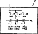
在图1A中,将读出放大器SA10的一个输入端经N沟道MOS晶体管(以下称为NMOS)N10连接到被选择的存储单元MC上,进而经作为负载的P沟道MOS晶体管(以下称为PMOS)P10连接到被供给电源电压Vdd的节点上。此外,将读出放大器SA10的另一个输入端连接到NMOSN11的一端上,进而经作为负载的P沟道MOS晶体管(以下称为PMOS)P11连接到被供给电源电压Vdd的节点上。该NMOSN11的另一端上连接了基准电流生成电路21。NMOSN10、N11是例如阈值电压被设定为0V的晶体管。In FIG. 1A, an input terminal of the sense amplifier SA10 is connected to the selected memory cell MC via an N-channel MOS transistor (hereinafter referred to as NMOS) N10, and then via a P-channel MOS transistor (hereinafter referred to as a load) as a load. PMOS) P10 is connected to a node supplied with power supply voltage Vdd. Also, the other input terminal of sense amplifier SA10 is connected to one terminal of NMOSN11, and further connected to a node supplied with power supply voltage Vdd via a P-channel MOS transistor (hereinafter referred to as PMOS) P11 as a load. The reference
图1B示出了基准电流生成电路21的一例。例如利用NMOSN12、N13、N14、基准存储单元RMC1、RMC2、RMC3构成了基准电流生成电路21。将NMOSN12、N13、N14的一端连接到NMOSN11的另一端上。将这些NMOSN12、N13、N14的另一端分别连接到基准存储单元RMC1、RMC2、RMC3上。这些基准存储单元RMC1、RMC2、RMC3是与存储单元的结构相同的EEPROM单元,分别被设定了例如不同的阈值电压Vth1、Vth2、Vth3。FIG. 1B shows an example of the reference
基准电流生成电路21的结构不限定于图1B,在将该电路应用于后述的电流校验的情况下,根据必要的校验电流的数目增加NMOSN12、N13、N14、基准存储单元RMC1、RMC2、RMC3即可。The structure of the reference
在将上述结构的读出放大器应用于校验用读出放大器3A的情况下,经字线WL对被选择的存储单元MC和基准存储单元RMC1-RMC3的控制栅供给同一电压。在该状态下,根据校验的阈值电压,信号φ1、φ2、φ3有选择地被定为高电平,从利用NMOSN12、N13、N14选择的基准存储单元RMC1、RMC2、RMC3的某一个输出作为基准电流的校验电流。利用读出放大器SA10比较该校验电流与流过被选择的存储单元MC的电流。将读出放大器SA10的输出信号供给控制器10。控制器10根据从读出放大器SA10供给的信号,控制对存储单元的写入。When the sense amplifier configured as described above is applied to verify
另一方面,在将上述结构的读出放大器SA10应用于读出用读出放大器3B的情况下,在数据读出时,经字线WL对被选择的存储单元MC和基准存储单元RMC1-RMC3的控制栅供给同一电压。在该状态下,首先,例如NMOSN13根据信号φ2被导通。在该状态下,利用读出放大器SA10检出流过基准存储单元RMC2的电流和流过存储单元MC的电流。其后,在从读出放大器SA10输出的信号为“0”的情况下,NMOSN12根据信号φ1被导通,在从读出放大器SA10输出的信号为“1”的情况下,NMOSN14根据信号φ3被导通。这样,利用读出放大器SA10检出流过基准存储单元RMC1或RMC3的电流和流过存储单元MC的电流。利用根据信号φ2从读出放大器SA10输出的信号和根据信号φ1或φ3从读出放大器SA10输出的信号来生成2比特的数据。On the other hand, when the sense amplifier SA10 having the above-mentioned structure is applied to the sense amplifier 3B for reading, during data reading, the selected memory cell MC and the reference memory cells RMC1-RMC3 are connected via the word line WL. The control gate supplies the same voltage. In this state, first, for example, NMOSN13 is turned on by signal φ2. In this state, the current flowing through reference memory cell RMC2 and the current flowing through memory cell MC are detected by sense amplifier SA10. Thereafter, when the signal output from the sense amplifier SA10 is "0", the NMOSN12 is turned on by the signal φ1, and when the signal output from the sense amplifier SA10 is "1", the NMOSN14 is turned on by the signal φ3. conduction. In this way, the current flowing through reference memory cell RMC1 or RMC3 and the current flowing through memory cell MC are detected by sense amplifier SA10. 2-bit data is generated by using the signal output from the sense amplifier SA10 based on the signal φ2 and the signal output from the sense amplifier SA10 based on the signal φ1 or φ3.
此外,在数据写入时的校验动作中,对被选择的存储单元MC和基准存储单元的字线供给读出时的同一电位。此外,根据写入数据来选择信号φ1、φ2、φ3。在该状态下,利用读出放大器SA10检出并校验流过存储单元MC的电流和流过被选择的基准存储单元的电流。这样,与各写入数据对应地比较流过存储单元MC的电流和流过基准存储单元RMC的电流以确保容限。In addition, in the verify operation at the time of data writing, the same potential at the time of reading is supplied to the word line of the selected memory cell MC and the reference memory cell. In addition, signals φ1, φ2, and φ3 are selected according to write data. In this state, the current flowing through the memory cell MC and the current flowing through the selected reference memory cell are detected and verified by the sense amplifier SA10. In this way, the current flowing through the memory cell MC is compared with the current flowing through the reference memory cell RMC corresponding to each write data to secure a margin.
关于电流比较型读出方式,如图1A中所示,使用作为连接到读出放大器SA10上的负载的PMOSP10、P11放大、比较在数据读出时流过存储单元MC的电流和流过基准存储单元的基准电流。Regarding the current comparison type readout method, as shown in FIG. 1A, the current flowing through the memory cell MC at the time of data readout is amplified and compared with the current flowing through the reference memory cell MC using PMOSP10, P11 as a load connected to the sense amplifier SA10. The base current of the unit.
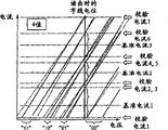
图5示出了2值中的电压校验方式,图6示出了4值中的电压校验方式。电压校验方式将校验时的字线电位设定为与读出时的字线电位不同的电位。在图5中示出的2值的情况下,将校验时的字线电位变化为校验电压1~校验电压4。此外,在图6中示出的4值的情况下,将校验时的字线电位变化为校验电压1~校验电压8。FIG. 5 shows the voltage verification method in 2 values, and FIG. 6 shows the voltage verification method in 4 values. In the voltage verification method, the potential of the word line at the time of verification is set to be different from the potential of the word line at the time of reading. In the case of the binary value shown in FIG. 5 , the word line potential at the time of verification is changed from
这样,在改变了校验时和读出时的字线电位的情况下,如图5、图6中所示,可保证与校验时的字线电位对应的存储单元的电流。但是,起因于存储单元的Gm离散(用实线示出中央值,用虚线示出上限值、下限值),不能保证与读出时的字线电位对应的存储单元的电流。如图5中所示,在2值的情况下,即使如用虚线所示那样存储单元的Gm发生了离散,对于基准电流判断是“1”还是“0”用的电流容限都是充分的。In this way, when the word line potentials during verification and read are changed, as shown in FIGS. 5 and 6 , the current of the memory cell corresponding to the word line potential during verification can be ensured. However, since the Gm of the memory cell varies (the solid line shows the median value, and the dotted line shows the upper limit value and the lower limit value), the current of the memory cell corresponding to the word line potential at the time of reading cannot be guaranteed. As shown in FIG. 5, in the case of binary values, even if the Gm of the memory cell varies as shown by the dotted line, the current tolerance for judging whether the reference current is "1" or "0" is sufficient. .
但是,如图6中所示,在4值的情况下,与对于基准电流1的电流容限相比,对于基准电流2判别低位比特是“0”还是“1”用的电流容限和对于基准电流3判别高位比特是“0”还是“1”用的电流容限减小了。因而,不限于4值,在多值的情况下,难以使用上述的电压校验方式。However, as shown in FIG. 6, in the case of 4 values, compared with the current tolerance for the reference current 1, the current tolerance for judging whether the lower bit is "0" or "1" for the reference current 2 is the same as for the current tolerance for the reference current 1. The current tolerance for the reference current 3 to judge whether the upper bit is "0" or "1" is reduced. Therefore, it is not limited to four values, and in the case of multiple values, it is difficult to use the above-mentioned voltage verification method.
因此,第1实施形态使校验时的字线电位与读出时的字线电位为同一电位,利用读出放大器检出流过存储单元MC的电流和流过基准存储单元的电流。Therefore, in the first embodiment, the word line potential at the time of verification is set to the same potential as the word line potential at the time of reading, and the current flowing through the memory cell MC and the current flowing through the reference memory cell are detected by the sense amplifier.
图7示出了与第1实施形态有关的2值的校验方式,图8示出了与第1实施形态有关的4值的校验方式。FIG. 7 shows a binary check method according to the first embodiment, and FIG. 8 shows a quadruple check method according to the first embodiment.
使校验时的存储单元的字线电位与读出时的字线电位为同一电位,将基准电流改变为所希望的电流值。于是,对于各基准电流来说,与存储单元的阈值电压(数据)对应的校验电流比以前大。因此,根据存储单元的各阈值电压,可确保读出电流的容限。The word line potential of the memory cell during verification is set to be the same potential as the word line potential during reading, and the reference current is changed to a desired current value. Therefore, for each reference current, the verification current corresponding to the threshold voltage (data) of the memory cell is larger than before. Therefore, a read current margin can be ensured according to each threshold voltage of the memory cell.
按照上述第1实施形态,使校验时的字线电位与读出时的字线电位为同一电位,通过比较流过存储单元MC的电流和流过基准存储单元的电流,校验存储单元的阈值电压。在该电流校验的情况下,在存储单元中被设定的阈值电压的离散变大,但在读出时,可增加与各数据对应的电流容限。因而,能进行可靠的读出。According to the above-mentioned first embodiment, the potential of the word line at the time of verification is set to the same potential as the potential of the word line at the time of reading, and by comparing the current flowing through the memory cell MC with the current flowing through the reference memory cell, the memory cell is verified. threshold voltage. In the case of this current verification, the threshold voltages set in the memory cells vary greatly, but at the time of reading, the current tolerance corresponding to each data can be increased. Therefore, reliable readout can be performed.
(第2实施形态)(Second Embodiment)
如上所述,在第1实施形态的情况下,由于阈值电压的离散变大,故不能充分地确保阈值的容限。例如,即使在根据写入数据将存储单元设定为“0”或“00”的情况下,在因随时间的变化在存储单元被写入的电子稍微地减少的情况下,也存在难以正确地读出数据的可能性。As described above, in the case of the first embodiment, since the variation of the threshold voltage becomes large, it is not possible to sufficiently secure the threshold tolerance. For example, even when the memory cell is set to "0" or "00" according to the written data, it is difficult to correctly write the electrons in the memory cell due to a slight decrease in electrons written in the memory cell due to changes over time. Possibility to read out data.
此外,在NOR型闪速存储器的情况下,多个存储单元并列地连接到同一位线上。因此,在存储单元中设定了“1”或“11”的情况下,该存储单元在非选择的情况下必须是关断状态。但是,如果流过关断状态的存储单元的电流变大,则也存在不能正确地读数据的可能性。Also, in the case of a NOR flash memory, a plurality of memory cells are connected in parallel to the same bit line. Therefore, when "1" or "11" is set in a memory cell, the memory cell must be in an OFF state when it is not selected. However, if the current flowing through the off-state memory cell increases, data may not be read correctly.
因此,第2实施形态通过按不同的用途组合电压校验和电流校验来使用,分别确保读出电流容限和阈值电压容限。Therefore, in the second embodiment, voltage calibration and current calibration are used in combination according to different applications, and the read current margin and the threshold voltage margin are ensured respectively.
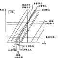
图9示出了第2实施形态的动作。在正确的读出电流容限为必要的校验中使用电流校验,在正确的阈值电压容限为必要的校验中使用电压校验。Fig. 9 shows the operation of the second embodiment. Current verification is used in verification where correct sense current tolerance is necessary, and voltage verification is used in verification where correct threshold voltage tolerance is necessary.
即,在数据“00”的最高阈值电压的校验中,在使用了图8中示出的那样的电流校验的情况下,读出时的字线电位与阈值电压的电位差很小。因此,在阈值电压因随时间的变化而变化的情况下,存在读出数据变化的危险。因此,与数据“00”对应的阈值电压的上限和下限必须比读出时的字线电位充分地高。因而,由于关于数据“00”的校验,电流校验是不适当的,故使用电压校验正确地控制阈值电压。That is, when the current verification as shown in FIG. 8 is used in the verification of the highest threshold voltage of data "00", the potential difference between the word line potential and the threshold voltage at the time of reading is small. Therefore, when the threshold voltage changes with time, the read data may change. Therefore, the upper limit and lower limit of the threshold voltage corresponding to the data "00" must be sufficiently higher than the word line potential at the time of reading. Thus, since the current verification is not appropriate regarding the verification of the data "00", the threshold voltage is correctly controlled using the voltage verification.
此外,即使关于与数据“11”对应的阈值电压的下限,也使用电压校验。在对于数据“11”的校验应用了电流校验的情况下,存在发生阈值低的存储单元的可能性,因此,有时在非选择时不充分地关断。因而,对于数据“11”的下限侧的校验,应用电流校验是不适当的,故使用电压校验。Furthermore, even with regard to the lower limit of the threshold voltage corresponding to the data "11", the voltage check is used. When the current verification is applied to the verification of the data "11", there is a possibility that a memory cell with a low threshold value may be generated, and therefore may not be sufficiently turned off at the time of non-selection. Therefore, for the verification of the lower limit side of the data "11", it is inappropriate to apply the current verification, so the voltage verification is used.
根据写入数据,控制器10转换电流校验和电压校验。控制器10在数据擦除后,对数据“11”的下限侧的校验进行电压校验,对上限侧的校验进行电流校验。According to the written data, the
图10示出了数据写入时的控制器10的动作。控制器10判别写入数据(S1),在写入数据为“00”的情况下,在数据写入后,进行电压校验(S2、S3)。在写入数据为“01”和“10”的情况下,在数据写入后,进行电流校验(S5、S6)。在电压校验(S3)的情况下,控制器10控制基准电流生成电路21,根据写入数据来生成基准电流。再者,控制器10控制第1电压生成电路8来变更字线的电压。在该状态下,进行电压校验,判别校验是否已结束(S4)。其结果,在写入不充分的情况下,再次执行数据的写入和电压校验。FIG. 10 shows the operation of the
另一方面,在电流校验的情况下(S6),控制器10控制第1电压生成电路8,将字线的电压设定为与读出电压为同一电压。再者,控制器10控制基准电流生成电路21,发生与写入数据对应的基准电流。在该状态下,进行电流校验,判别校验是否已结束(S7)。其结果,在写入不充分的情况下,再次执行数据的写入和电流校验。通过重复这样的动作来设定存储单元的阈值电压。On the other hand, in the case of current verification (S6), the
按照上述第2实施形态,关于读出电流容限为必要的数据的写入校验,使用了电流校验,关于正确的阈值电压的控制为必要的数据的写入校验,使用了电压校验。因此,在数据的读出时,可防止数据的读出错误的发生,而且,可得到在读出中必要且充分的电流容限。According to the above-mentioned second embodiment, current verification is used for writing verification of data that requires a read current margin, and voltage verification is used for writing verification of data that requires accurate threshold voltage control. test. Therefore, at the time of data reading, it is possible to prevent the occurrence of a data reading error, and to obtain a current margin necessary and sufficient for reading.
(第3实施形态)(third embodiment)
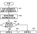
如上所述,存储单元的Gm的离散对读出电流容限和阈值电压容限有很大的影响。因此,在第3实施形态中,说明容易地检测存储单元的Gm超过了规定值的异常存储单元的方法。As described above, the variation in Gm of a memory cell has a great influence on the read current tolerance and the threshold voltage tolerance. Therefore, in the third embodiment, a method of easily detecting an abnormal memory cell whose Gm of the memory cell exceeds a predetermined value will be described.
如图11中所示,首先,使用电流校验将存储单元的阈值电压调整为例如4值的数据“10”。其次,利用电压校验测定该存储单元的阈值电压分布。可预先预测与数据“10”对应的Gm的阈值分布。因此,可容易地检测显示出预先被预测的规定值以外的阈值电压的存储单元作为异常存储单元。As shown in FIG. 11, first, the threshold voltage of the memory cell is adjusted to, for example, 4-valued data "10" using the current verify. Next, the threshold voltage distribution of the memory cell is determined by voltage calibration. The threshold distribution of Gm corresponding to data "10" can be predicted in advance. Therefore, a memory cell exhibiting a threshold voltage other than a predetermined value predicted in advance can be easily detected as an abnormal memory cell.
图12示出了控制器10的动作。控制器10在检出异常存储单元的情况下,首先对利用电流校验选择的存储单元例如设定数据“10”(S11)。即,在对被选择的存储单元写入了数据后,利用第1电压生成电路8使字线的电位设定为读出时的电位。再者,控制器10利用基准电流生成电路21生成与数据“10”对应的校验用的基准电流。FIG. 12 shows the action of the
这样,在对存储单元设定了与数据“10”对应的阈值电压后,利用电压校验测定在存储单元中被设定的阈值电压(S12)。即,控制器10利用基准电流生成电路21生成与读出时的数据“10”对应的基准电流。与此同时,控制器10利用第1电压生成电路8生成与数据“10”对应的校验电压。即,例如,首先生成与数据“10”的阈值电压的下限对应的电压。在该状态下,利用读出放大器SA10比较流过存储单元的电流与基准电流。其次,生成与数据“10”的阈值电压的上限对应的电压。在该状态下,利用读出放大器SA10比较流过存储单元的电流与基准电流。这样,利用电压校验测定在存储单元中被设定的阈值电压。In this way, after the threshold voltage corresponding to the data "10" is set in the memory cell, the threshold voltage set in the memory cell is measured by voltage verification (S12). That is, the
其次,比较被测定的阈值电压与预先被测定的数据“10”的阈值电压分布的规定值(S13)。其结果,在规定值以内的情况被判别为正常的存储单元(S14),在规定值以外的情况被判别为异常的存储单元(S15)。Next, the measured threshold voltage is compared with the predetermined value of the threshold voltage distribution of data "10" measured in advance (S13). As a result, those within the predetermined value are judged as normal memory cells ( S14 ), and those outside the predetermined value are judged as abnormal memory cells ( S15 ).
按照上述第3实施形态,使用电流校验和电压校验,可检出Gm异常的存储单元。因此,可预先清除异常的存储单元。再者,通过将该异常的存储单元转换为未图示的冗余存储单元,可提高存储单元的成品率。According to the above-mentioned third embodiment, a memory cell having an abnormal Gm can be detected by using the current verification and the voltage verification. Therefore, abnormal memory cells can be cleared in advance. Furthermore, by converting the abnormal memory cell into a redundant memory cell (not shown), the yield of the memory cell can be improved.
此外,上述各实施形态说明了存储多值数据的闪速存储器,但当然也可应用于存储2值数据的闪速存储器。In addition, each of the above-mentioned embodiments has described a flash memory that stores multi-valued data, but it is of course also applicable to a flash memory that stores binary data.
此外,基准电流生成电路21的结构不限定于图1A、1B,可构成为例如设置1个基准存储单元,对电流比例不同的多个电流镜电路供给流过该基准存储单元的电流,从这些电流镜电路输出多个基准电流。In addition, the configuration of the reference
对于本领域的专业人员来说,可容易地实现本发明的附加的优点和变型。因而,本发明在其更宽的方面不限于在这里示出的和描述的特定的细节和代表性的实施例。因此,在不偏离由后附的权利要求及其等效内容所限定的本发明的普遍性的概念的精神和范围的情况下,可作各种各样的修正。Additional advantages and modifications of the invention will readily occur to those skilled in the art. Therefore, the invention in its broader aspects is not limited to the specific details and representative embodiments shown and described herein. Accordingly, various modifications may be made without departing from the spirit and scope of the general concept of the invention as defined by the appended claims and their equivalents.
Claims (4)
Applications Claiming Priority (2)
| Application Number | Priority Date | Filing Date | Title |
|---|---|---|---|
| JP2005114750 | 2005-04-12 | ||
| JP2005114750A JP2006294144A (en) | 2005-04-12 | 2005-04-12 | Nonvolatile semiconductor memory device |
Publications (2)
| Publication Number | Publication Date |
|---|---|
| CN1848294A CN1848294A (en) | 2006-10-18 |
| CN100541663C true CN100541663C (en) | 2009-09-16 |
Family
ID=37077809
Family Applications (1)
| Application Number | Title | Priority Date | Filing Date |
|---|---|---|---|
| CNB2006100735107A Expired - Lifetime CN100541663C (en) | 2005-04-12 | 2006-04-12 | Non-volatile semiconductor memory for storing multi-valued data |
Country Status (4)
| Country | Link |
|---|---|
| US (3) | US7397716B2 (en) |
| JP (1) | JP2006294144A (en) |
| KR (1) | KR100785185B1 (en) |
| CN (1) | CN100541663C (en) |
Families Citing this family (11)
| Publication number | Priority date | Publication date | Assignee | Title |
|---|---|---|---|---|
| KR100850509B1 (en) * | 2007-01-10 | 2008-08-05 | 삼성전자주식회사 | Program method of multi bit flash memory device for reducing a program error |
| US7729165B2 (en) * | 2007-03-29 | 2010-06-01 | Flashsilicon, Incorporation | Self-adaptive and self-calibrated multiple-level non-volatile memories |
| KR100837282B1 (en) | 2007-06-14 | 2008-06-12 | 삼성전자주식회사 | Non-volatile memory device, memory system comprising it, its program method and read method |
| US7778098B2 (en) * | 2007-12-31 | 2010-08-17 | Cypress Semiconductor Corporation | Dummy cell for memory circuits |
| KR101553375B1 (en) * | 2009-04-30 | 2015-09-16 | 삼성전자주식회사 | Flash memory device |
| US9666246B2 (en) * | 2013-09-11 | 2017-05-30 | Taiwan Semiconductor Manufacturing Company, Ltd. | Dynamic reference current sensing |
| CN113918481A (en) * | 2017-07-30 | 2022-01-11 | 纽罗布拉德有限公司 | Memory chip |
| CN108198587B (en) * | 2017-12-21 | 2024-03-19 | 珠海博雅科技股份有限公司 | Reference current generating circuit and reference current generating method |
| KR102409791B1 (en) * | 2017-12-27 | 2022-06-16 | 에스케이하이닉스 주식회사 | Semiconductor memory device and method for operating thereof |
| CN110137348B (en) * | 2019-04-11 | 2023-01-31 | 上海集成电路研发中心有限公司 | A Multiplexing Multi-valued Resistive Switching Structure and Its Neural Network Formed |
| US11169587B2 (en) * | 2020-01-10 | 2021-11-09 | Micron Technology, Inc. | Feedback for power management of a memory die using a dedicated pin |
Citations (4)
| Publication number | Priority date | Publication date | Assignee | Title |
|---|---|---|---|---|
| CN1423279A (en) * | 2001-12-03 | 2003-06-11 | 三菱电机株式会社 | Semiconductor storage device reading data according to current passing through storage anit while accessing |
| US6650570B2 (en) * | 2000-09-22 | 2003-11-18 | Kabushiki Kaisha Toshiba | Non-volatile semiconductor memory |
| US6768191B2 (en) * | 2001-08-10 | 2004-07-27 | Infineon Technologies Ag | Electronic component with stacked electronic elements |
| US6816413B2 (en) * | 2002-07-15 | 2004-11-09 | Kabushiki Kaishi Toshiba | Nonvolatile semiconductor memory capable of generating read-mode reference current and verify-mode reference current from the same reference cell |
Family Cites Families (28)
| Publication number | Priority date | Publication date | Assignee | Title |
|---|---|---|---|---|
| US6222762B1 (en) * | 1992-01-14 | 2001-04-24 | Sandisk Corporation | Multi-state memory |
| US5532962A (en) * | 1992-05-20 | 1996-07-02 | Sandisk Corporation | Soft errors handling in EEPROM devices |
| EP0686979B1 (en) * | 1994-06-10 | 2001-03-07 | STMicroelectronics S.r.l. | Failure tolerant memory device, in particular of the flash EEPROM type |
| KR0172401B1 (en) * | 1995-12-07 | 1999-03-30 | 김광호 | Multistate Nonvolatile Semiconductor Memory Devices |
| DE69702256T2 (en) * | 1996-06-24 | 2001-01-18 | Advanced Micro Devices, Inc. | METHOD FOR A MULTIPLE, BITS PER CELL FLASH EEPROM, MEMORY WITH SIDE PROGRAMMING MODE, AND READING METHOD |
| TW365001B (en) * | 1996-10-17 | 1999-07-21 | Hitachi Ltd | Non-volatile semiconductor memory apparatus and the operation method |
| US7139196B2 (en) * | 1999-01-14 | 2006-11-21 | Silicon Storage Technology, Inc. | Sub-volt sensing for digital multilevel flash memory |
| JP4047515B2 (en) | 1999-05-10 | 2008-02-13 | 株式会社東芝 | Semiconductor device |
| JP3569185B2 (en) * | 1999-12-24 | 2004-09-22 | Necエレクトロニクス株式会社 | Nonvolatile semiconductor memory device |
| JP3611497B2 (en) * | 2000-03-02 | 2005-01-19 | 松下電器産業株式会社 | Current sense amplifier |
| US6222761B1 (en) * | 2000-07-17 | 2001-04-24 | Microchip Technology Incorporated | Method for minimizing program disturb in a memory cell |
| US7071771B2 (en) * | 2000-12-11 | 2006-07-04 | Kabushiki Kaisha Toshiba | Current difference divider circuit |
| JP2002184190A (en) * | 2000-12-11 | 2002-06-28 | Toshiba Corp | Nonvolatile semiconductor memory device |
| US6493266B1 (en) * | 2001-04-09 | 2002-12-10 | Advanced Micro Devices, Inc. | Soft program and soft program verify of the core cells in flash memory array |
| JP3984445B2 (en) * | 2001-09-12 | 2007-10-03 | シャープ株式会社 | Overerase cell detection method for nonvolatile semiconductor memory device |
| JP2003257192A (en) * | 2002-03-06 | 2003-09-12 | Mitsubishi Electric Corp | Semiconductor storage device and nonvolatile semiconductor storage device |
| KR100463954B1 (en) * | 2002-05-17 | 2004-12-30 | 주식회사 하이닉스반도체 | Flash memory device and method of erasing the same |
| JP4260434B2 (en) * | 2002-07-16 | 2009-04-30 | 富士通マイクロエレクトロニクス株式会社 | Nonvolatile semiconductor memory and operation method thereof |
| US6903965B2 (en) * | 2002-07-18 | 2005-06-07 | Renesas Technology Corp. | Thin film magnetic memory device permitting high precision data read |
| JP4144784B2 (en) * | 2002-07-30 | 2008-09-03 | シャープ株式会社 | Read circuit of semiconductor memory device, reference circuit thereof, and semiconductor memory device |
| US6618297B1 (en) * | 2002-08-02 | 2003-09-09 | Atmel Corporation | Method of establishing reference levels for sensing multilevel memory cell states |
| ITMI20022569A1 (en) * | 2002-12-05 | 2004-06-06 | Simicroelectronics S R L | PROGRAMMING METHOD OF AN ELECTRONICALLY PROGRAMMABLE NON-VOLATILE SEMICONDUCTOR MEMORY |
| ITMI20022570A1 (en) * | 2002-12-05 | 2004-06-06 | Simicroelectronics S R L | PROGRAMMING METHOD OF AN ELECTRICALLY PROGRAMMABLE NON-VOLATILE SEMICONDUCTOR MEMORY |
| US6882567B1 (en) * | 2002-12-06 | 2005-04-19 | Multi Level Memory Technology | Parallel programming of multiple-bit-per-cell memory cells on a continuous word line |
| ITMI20030075A1 (en) * | 2003-01-20 | 2004-07-21 | Simicroelectronics S R L | PARALLEL DETECTION AMPLIFIER WITH CURRENT MIRROR TO BE MEASURED ON EACH REFERENCE BRANCH. |
| JP4270898B2 (en) * | 2003-02-07 | 2009-06-03 | Necエレクトロニクス株式会社 | Nonvolatile semiconductor memory device |
| US6912150B2 (en) * | 2003-05-13 | 2005-06-28 | Lionel Portman | Reference current generator, and method of programming, adjusting and/or operating same |
| JP4469649B2 (en) * | 2003-09-17 | 2010-05-26 | 株式会社ルネサステクノロジ | Semiconductor flash memory |
-
2005
- 2005-04-12 JP JP2005114750A patent/JP2006294144A/en active Pending
-
2006
- 2006-04-11 US US11/401,286 patent/US7397716B2/en not_active Expired - Lifetime
- 2006-04-11 KR KR1020060032612A patent/KR100785185B1/en not_active Expired - Lifetime
- 2006-04-12 CN CNB2006100735107A patent/CN100541663C/en not_active Expired - Lifetime
-
2007
- 2007-06-15 US US11/763,743 patent/US7420863B2/en not_active Expired - Fee Related
- 2007-06-15 US US11/763,690 patent/US7414892B2/en not_active Expired - Lifetime
Patent Citations (4)
| Publication number | Priority date | Publication date | Assignee | Title |
|---|---|---|---|---|
| US6650570B2 (en) * | 2000-09-22 | 2003-11-18 | Kabushiki Kaisha Toshiba | Non-volatile semiconductor memory |
| US6768191B2 (en) * | 2001-08-10 | 2004-07-27 | Infineon Technologies Ag | Electronic component with stacked electronic elements |
| CN1423279A (en) * | 2001-12-03 | 2003-06-11 | 三菱电机株式会社 | Semiconductor storage device reading data according to current passing through storage anit while accessing |
| US6816413B2 (en) * | 2002-07-15 | 2004-11-09 | Kabushiki Kaishi Toshiba | Nonvolatile semiconductor memory capable of generating read-mode reference current and verify-mode reference current from the same reference cell |
Also Published As
| Publication number | Publication date |
|---|---|
| JP2006294144A (en) | 2006-10-26 |
| CN1848294A (en) | 2006-10-18 |
| US7420863B2 (en) | 2008-09-02 |
| US7414892B2 (en) | 2008-08-19 |
| KR100785185B1 (en) | 2007-12-11 |
| KR20060108230A (en) | 2006-10-17 |
| US20070242517A1 (en) | 2007-10-18 |
| US20070236998A1 (en) | 2007-10-11 |
| US7397716B2 (en) | 2008-07-08 |
| US20060227619A1 (en) | 2006-10-12 |
Similar Documents
| Publication | Publication Date | Title |
|---|---|---|
| CN1848299B (en) | Reference current generating circuit for nonvolatile semiconductor memory device | |
| JP3987715B2 (en) | Nonvolatile semiconductor memory and program voltage control method for nonvolatile semiconductor memory | |
| US7414892B2 (en) | Nonvolatile semiconductor memory device which stores multivalue data | |
| JP2006012367A (en) | Nonvolatile semiconductor memory device | |
| JP3906189B2 (en) | Nonvolatile semiconductor memory | |
| KR100660534B1 (en) | Program Verification Method of Nonvolatile Memory Device | |
| JP5909294B1 (en) | WRITE CIRCUIT AND METHOD FOR NONVOLATILE MEMORY DEVICE, AND NONVOLATILE MEMORY DEVICE | |
| JP6114796B1 (en) | Sense circuit for nonvolatile memory device and nonvolatile memory device | |
| JPWO2004097839A1 (en) | Nonvolatile semiconductor memory device and method for programming nonvolatile semiconductor memory device | |
| JP4762986B2 (en) | Nonvolatile memory device and control method of nonvolatile memory device | |
| US7315475B2 (en) | Non-volatile semiconductor memory device | |
| JP4988190B2 (en) | Nonvolatile semiconductor memory | |
| JP2007035179A (en) | Nonvolatile semiconductor memory device | |
| US12494263B2 (en) | Flash memory for performing margin read test operation and margin read test system including the same | |
| JP2005149625A (en) | Semiconductor memory | |
| JP5454949B2 (en) | Semiconductor memory device | |
| KR100757126B1 (en) | Nonvolatile semiconductor memory | |
| JP4004527B2 (en) | Multi-state EEPROM read / write circuit | |
| JP5475975B2 (en) | Semiconductor device and adjustment method thereof | |
| JP2010231887A (en) | Nonvolatile semiconductor memory | |
| JP2007109360A (en) | Semiconductor memory device reading method and semiconductor memory device | |
| JP2006216196A (en) | Nonvolatile semiconductor memory device | |
| JP2007213719A (en) | Semiconductor memory device |
Legal Events
| Date | Code | Title | Description |
|---|---|---|---|
| C06 | Publication | ||
| PB01 | Publication | ||
| C10 | Entry into substantive examination | ||
| SE01 | Entry into force of request for substantive examination | ||
| C14 | Grant of patent or utility model | ||
| GR01 | Patent grant | ||
| TR01 | Transfer of patent right |
Effective date of registration: 20170728 Address after: Tokyo, Japan Patentee after: TOSHIBA MEMORY Corp. Address before: Tokyo, Japan Patentee before: Toshiba Corp. |
|
| TR01 | Transfer of patent right | ||
| CP01 | Change in the name or title of a patent holder |
Address after: Tokyo Patentee after: Kaixia Co.,Ltd. Address before: Tokyo Patentee before: TOSHIBA MEMORY Corp. Address after: Tokyo Patentee after: TOSHIBA MEMORY Corp. Address before: Tokyo Patentee before: Japanese businessman Panjaya Co.,Ltd. |
|
| CP01 | Change in the name or title of a patent holder | ||
| TR01 | Transfer of patent right |
Effective date of registration: 20211129 Address after: Tokyo Patentee after: Japanese businessman Panjaya Co.,Ltd. Address before: Tokyo Patentee before: TOSHIBA MEMORY Corp. |
|
| TR01 | Transfer of patent right | ||
| CX01 | Expiry of patent term |
Granted publication date: 20090916 |