CN100470844C - Spin transistor using spin filter effect and nonvolatile memory using spin transistor - Google Patents
Spin transistor using spin filter effect and nonvolatile memory using spin transistor Download PDFInfo
- Publication number
- CN100470844C CN100470844C CNB038224801A CN03822480A CN100470844C CN 100470844 C CN100470844 C CN 100470844C CN B038224801 A CNB038224801 A CN B038224801A CN 03822480 A CN03822480 A CN 03822480A CN 100470844 C CN100470844 C CN 100470844C
- Authority
- CN
- China
- Prior art keywords
- spin
- transistor
- base stage
- barrier layer
- emitter
- Prior art date
- Legal status (The legal status is an assumption and is not a legal conclusion. Google has not performed a legal analysis and makes no representation as to the accuracy of the status listed.)
- Expired - Fee Related
Links
- 230000000694 effects Effects 0.000 title claims description 40
- 230000004888 barrier function Effects 0.000 claims abstract description 203
- 230000005294 ferromagnetic effect Effects 0.000 claims abstract description 164
- 230000005415 magnetization Effects 0.000 claims description 125
- 239000002800 charge carrier Substances 0.000 claims description 53
- 239000004065 semiconductor Substances 0.000 claims description 46
- 239000003302 ferromagnetic material Substances 0.000 claims description 30
- 238000003860 storage Methods 0.000 claims description 20
- 229910052751 metal Inorganic materials 0.000 claims description 18
- 239000002184 metal Substances 0.000 claims description 18
- 230000008859 change Effects 0.000 claims description 17
- 238000005036 potential barrier Methods 0.000 claims description 10
- 239000000126 substance Substances 0.000 claims description 8
- 238000001514 detection method Methods 0.000 claims description 3
- 239000000969 carrier Substances 0.000 abstract description 6
- 230000005291 magnetic effect Effects 0.000 description 104
- 238000001914 filtration Methods 0.000 description 41
- 238000010586 diagram Methods 0.000 description 36
- 239000002784 hot electron Substances 0.000 description 19
- 230000003321 amplification Effects 0.000 description 11
- 238000003199 nucleic acid amplification method Methods 0.000 description 11
- 238000009413 insulation Methods 0.000 description 9
- 239000012212 insulator Substances 0.000 description 6
- 230000002093 peripheral effect Effects 0.000 description 6
- 230000008901 benefit Effects 0.000 description 5
- 238000002347 injection Methods 0.000 description 5
- 239000007924 injection Substances 0.000 description 5
- 238000000034 method Methods 0.000 description 5
- 238000009987 spinning Methods 0.000 description 5
- 230000005764 inhibitory process Effects 0.000 description 4
- 230000003068 static effect Effects 0.000 description 4
- 230000001413 cellular effect Effects 0.000 description 3
- 238000010276 construction Methods 0.000 description 3
- 239000013078 crystal Substances 0.000 description 3
- 230000005684 electric field Effects 0.000 description 3
- 239000011159 matrix material Substances 0.000 description 3
- 230000035807 sensation Effects 0.000 description 3
- 230000005641 tunneling Effects 0.000 description 3
- 230000015572 biosynthetic process Effects 0.000 description 2
- 239000012159 carrier gas Substances 0.000 description 2
- 230000005611 electricity Effects 0.000 description 2
- 230000005669 field effect Effects 0.000 description 2
- 230000006870 function Effects 0.000 description 2
- 230000010354 integration Effects 0.000 description 2
- 239000000463 material Substances 0.000 description 2
- 238000005303 weighing Methods 0.000 description 2
- 229910001218 Gallium arsenide Inorganic materials 0.000 description 1
- 229910002056 binary alloy Inorganic materials 0.000 description 1
- 239000012141 concentrate Substances 0.000 description 1
- 230000008878 coupling Effects 0.000 description 1
- 238000010168 coupling process Methods 0.000 description 1
- 238000005859 coupling reaction Methods 0.000 description 1
- 238000004134 energy conservation Methods 0.000 description 1
- 238000005516 engineering process Methods 0.000 description 1
- 229910052737 gold Inorganic materials 0.000 description 1
- 238000010438 heat treatment Methods 0.000 description 1
- 230000006872 improvement Effects 0.000 description 1
- 239000012535 impurity Substances 0.000 description 1
- 238000012423 maintenance Methods 0.000 description 1
- 238000004519 manufacturing process Methods 0.000 description 1
- 230000007246 mechanism Effects 0.000 description 1
- 229910044991 metal oxide Inorganic materials 0.000 description 1
- 150000004706 metal oxides Chemical class 0.000 description 1
- 150000002739 metals Chemical class 0.000 description 1
- 239000000203 mixture Substances 0.000 description 1
- 230000004048 modification Effects 0.000 description 1
- 238000012986 modification Methods 0.000 description 1
- 238000005457 optimization Methods 0.000 description 1
- 229910052761 rare earth metal Inorganic materials 0.000 description 1
- 230000035945 sensitivity Effects 0.000 description 1
- 238000004544 sputter deposition Methods 0.000 description 1
- 239000000758 substrate Substances 0.000 description 1
- 238000001771 vacuum deposition Methods 0.000 description 1
Images


Classifications
-
- H—ELECTRICITY
- H01—ELECTRIC ELEMENTS
- H01L—SEMICONDUCTOR DEVICES NOT COVERED BY CLASS H10
- H01L27/00—Devices consisting of a plurality of semiconductor or other solid-state components formed in or on a common substrate
- H01L27/02—Devices consisting of a plurality of semiconductor or other solid-state components formed in or on a common substrate including semiconductor components specially adapted for rectifying, oscillating, amplifying or switching and having at least one potential-jump barrier or surface barrier; including integrated passive circuit elements with at least one potential-jump barrier or surface barrier
- H01L27/04—Devices consisting of a plurality of semiconductor or other solid-state components formed in or on a common substrate including semiconductor components specially adapted for rectifying, oscillating, amplifying or switching and having at least one potential-jump barrier or surface barrier; including integrated passive circuit elements with at least one potential-jump barrier or surface barrier the substrate being a semiconductor body
- H01L27/10—Devices consisting of a plurality of semiconductor or other solid-state components formed in or on a common substrate including semiconductor components specially adapted for rectifying, oscillating, amplifying or switching and having at least one potential-jump barrier or surface barrier; including integrated passive circuit elements with at least one potential-jump barrier or surface barrier the substrate being a semiconductor body including a plurality of individual components in a repetitive configuration
- H01L27/105—Devices consisting of a plurality of semiconductor or other solid-state components formed in or on a common substrate including semiconductor components specially adapted for rectifying, oscillating, amplifying or switching and having at least one potential-jump barrier or surface barrier; including integrated passive circuit elements with at least one potential-jump barrier or surface barrier the substrate being a semiconductor body including a plurality of individual components in a repetitive configuration including field-effect components
-
- H—ELECTRICITY
- H01—ELECTRIC ELEMENTS
- H01L—SEMICONDUCTOR DEVICES NOT COVERED BY CLASS H10
- H01L29/00—Semiconductor devices adapted for rectifying, amplifying, oscillating or switching, or capacitors or resistors with at least one potential-jump barrier or surface barrier, e.g. PN junction depletion layer or carrier concentration layer; Details of semiconductor bodies or of electrodes thereof ; Multistep manufacturing processes therefor
- H01L29/66—Types of semiconductor device ; Multistep manufacturing processes therefor
- H01L29/66984—Devices using spin polarized carriers
-
- G—PHYSICS
- G11—INFORMATION STORAGE
- G11C—STATIC STORES
- G11C11/00—Digital stores characterised by the use of particular electric or magnetic storage elements; Storage elements therefor
- G11C11/02—Digital stores characterised by the use of particular electric or magnetic storage elements; Storage elements therefor using magnetic elements
- G11C11/14—Digital stores characterised by the use of particular electric or magnetic storage elements; Storage elements therefor using magnetic elements using thin-film elements
- G11C11/15—Digital stores characterised by the use of particular electric or magnetic storage elements; Storage elements therefor using magnetic elements using thin-film elements using multiple magnetic layers
-
- G—PHYSICS
- G11—INFORMATION STORAGE
- G11C—STATIC STORES
- G11C11/00—Digital stores characterised by the use of particular electric or magnetic storage elements; Storage elements therefor
- G11C11/02—Digital stores characterised by the use of particular electric or magnetic storage elements; Storage elements therefor using magnetic elements
- G11C11/16—Digital stores characterised by the use of particular electric or magnetic storage elements; Storage elements therefor using magnetic elements using elements in which the storage effect is based on magnetic spin effect
-
- H—ELECTRICITY
- H01—ELECTRIC ELEMENTS
- H01L—SEMICONDUCTOR DEVICES NOT COVERED BY CLASS H10
- H01L29/00—Semiconductor devices adapted for rectifying, amplifying, oscillating or switching, or capacitors or resistors with at least one potential-jump barrier or surface barrier, e.g. PN junction depletion layer or carrier concentration layer; Details of semiconductor bodies or of electrodes thereof ; Multistep manufacturing processes therefor
- H01L29/66—Types of semiconductor device ; Multistep manufacturing processes therefor
- H01L29/82—Types of semiconductor device ; Multistep manufacturing processes therefor controllable by variation of the magnetic field applied to the device
-
- H—ELECTRICITY
- H01—ELECTRIC ELEMENTS
- H01L—SEMICONDUCTOR DEVICES NOT COVERED BY CLASS H10
- H01L29/00—Semiconductor devices adapted for rectifying, amplifying, oscillating or switching, or capacitors or resistors with at least one potential-jump barrier or surface barrier, e.g. PN junction depletion layer or carrier concentration layer; Details of semiconductor bodies or of electrodes thereof ; Multistep manufacturing processes therefor
- H01L29/66—Types of semiconductor device ; Multistep manufacturing processes therefor
- H01L29/68—Types of semiconductor device ; Multistep manufacturing processes therefor controllable by only the electric current supplied, or only the electric potential applied, to an electrode which does not carry the current to be rectified, amplified or switched
- H01L29/70—Bipolar devices
- H01L29/72—Transistor-type devices, i.e. able to continuously respond to applied control signals
- H01L29/73—Bipolar junction transistors
-
- H—ELECTRICITY
- H01—ELECTRIC ELEMENTS
- H01L—SEMICONDUCTOR DEVICES NOT COVERED BY CLASS H10
- H01L29/00—Semiconductor devices adapted for rectifying, amplifying, oscillating or switching, or capacitors or resistors with at least one potential-jump barrier or surface barrier, e.g. PN junction depletion layer or carrier concentration layer; Details of semiconductor bodies or of electrodes thereof ; Multistep manufacturing processes therefor
- H01L29/66—Types of semiconductor device ; Multistep manufacturing processes therefor
- H01L29/68—Types of semiconductor device ; Multistep manufacturing processes therefor controllable by only the electric current supplied, or only the electric potential applied, to an electrode which does not carry the current to be rectified, amplified or switched
- H01L29/76—Unipolar devices, e.g. field effect transistors
- H01L29/772—Field effect transistors
- H01L29/778—Field effect transistors with two-dimensional charge carrier gas channel, e.g. HEMT ; with two-dimensional charge-carrier layer formed at a heterojunction interface
-
- H—ELECTRICITY
- H01—ELECTRIC ELEMENTS
- H01L—SEMICONDUCTOR DEVICES NOT COVERED BY CLASS H10
- H01L29/00—Semiconductor devices adapted for rectifying, amplifying, oscillating or switching, or capacitors or resistors with at least one potential-jump barrier or surface barrier, e.g. PN junction depletion layer or carrier concentration layer; Details of semiconductor bodies or of electrodes thereof ; Multistep manufacturing processes therefor
- H01L29/66—Types of semiconductor device ; Multistep manufacturing processes therefor
- H01L29/68—Types of semiconductor device ; Multistep manufacturing processes therefor controllable by only the electric current supplied, or only the electric potential applied, to an electrode which does not carry the current to be rectified, amplified or switched
- H01L29/76—Unipolar devices, e.g. field effect transistors
- H01L29/772—Field effect transistors
- H01L29/78—Field effect transistors with field effect produced by an insulated gate
-
- H—ELECTRICITY
- H10—SEMICONDUCTOR DEVICES; ELECTRIC SOLID-STATE DEVICES NOT OTHERWISE PROVIDED FOR
- H10N—ELECTRIC SOLID-STATE DEVICES NOT OTHERWISE PROVIDED FOR
- H10N50/00—Galvanomagnetic devices
- H10N50/10—Magnetoresistive devices
Abstract
A spin transistor comprises a spin injector for injecting, from a first nonmagnetic electrode carriers with a spin parallel to a spin band forming the band edge of a first ferromagnetic barrier layer, to a second nonmagnetic electrode layer, as hot carriers. It also comprises a spin analyzer whereby, due to spin-splitting at the band edge of a second ferromagnetic barrier layer, the spin-polarized hot carriers are transported to a third nonmagnetic electrode when the direction of the spin of the carriers injected into the second nonmagnetic electrode is parallel to that of the spin of the spin band at the band edge of the second ferromagnetic barrier layer, whereas the hot carriers are not transported to the third nonmagnetic electrode in the case of antiparallel spin. A memory element is also provided that comprises such a spin transistor.
Description
Technical field
The present invention relates to a kind of novel transistor.More particularly, the present invention relates to a kind of transistor with the output characteristic that depends on the charge carrier spin direction and utilize the transistorized non-volatile memory circuits of described kind (nonvolatile storage).
Background technology
It seems the semiconductor memory that DRAM (dynamic random access memory) mainly uses as the electronic equipment that with the microcomputer is representative from the viewpoint of operating rate and integrated level.In DRAM, the problem of the contents lost of being stored when wanting consumed energy and outage owing to the maintenance memory is difficult to satisfy requirement energy-conservation in recent years and mobile device.In order to satisfy such requirement, importantly a kind of except that high speed, high integration and low-power consumption, the novel memory that also has non-volatile characteristic.
Equal DRAM's and memory of future generation with non-volatile characteristic as a kind of operating rate and integrated level of can realizing, attentiveness concentrates on the MRAM (magnetoresistive RAM).MRAM reads information according to its direction of magnetization according to the direction of magnetization stored information of ferromagnetic material and by the giant magnetoresistance effect of Spin Valve device or tunnel magnetoresistive (TMR) effect of magnetic tunnel-junction (MTJ) on electric.Use the MRAM of ferromagnetic material under not catabiotic situation, to preserve information in non-volatile mode.
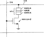
Figure 17 (A) and 17 (B) are the sketches of typical unit structure that expression utilizes the MRAM of MTJ.Shown in Figure 17 (A), in described MRAM, a memory cell is made of a MTJ and a MOS (metal-oxide semiconductor (MOS)) transistor.The grid of described MOS transistor is connected to sense word line, its source ground, and its drain electrode is connected to the end of MTJ, and the other end of MTJ is connected to bit line.
Shown in Figure 17 (B), MTJ has tunnel junction structure, and the latter has the thin dielectric film that inserts between two ferromagnetic electrodes, and described MTJ has the TMR effect, wherein tunnel resistor according to the relative direction of magnetization of two ferromagnetic electrodes difference.Specifically, the rate of change of TMR is called the TMR ratio when two ferromagnetic electrodes have parallel magnetization and when they have antiparallel magnetization, in order to calculate the effect of TMR.
MRAM adopts following method to come stored information: utilize by flow into bit line and with the resultant magnetic field of the current-induced of the rewriting word line (not shown) of its quadrature, make the magnetized state of MTJ, that is to say that the relative direction of magnetization of two ferromagnetic electrodes can be parallel magnetization or antiparallel magnetization.
In order to read the stored information that is stored in designating unit, apply a voltage to the appointment sense word line that connects described unit, so that make the MOS transistor conducting, read current (hereinafter referred to as " drive current ") from the specific bit linear flow that connects described unit to MTJ, and the voltage drop based on the MTJ of TMR effect is detected as output voltage, so that read described canned data.
Summary of the invention
Utilize the MRAM of MTJ to use ferromagnetic material, so that have non-volatile, low-power consumption and characteristic at a high speed.The structure of described unit is simplified, so that be applicable to that high density is integrated.The MRAM expection is as nonvolatile storage of future generation.In order to realize this point, need to solve following problem.
(1) MTJ has the binary system resistance value corresponding with parallel magnetization and antiparallel magnetization state.MRAM makes drive current flow to MTJ, so that detect described resistance value with the form of output voltage.In order to obtain high output voltage, must adjust the thickness of MTJ dielectric film so that optimize described tunnel resistor.Because the TMR ratio depends on the thickness of described dielectric film, so the optimization of tunnel resistor is restricted.
(2) for the information content of readout memory accurately, described TMR ratio must be big, so that increase the output voltage ratio of parallel magnetization and two magnetized states of antiparallel magnetization.In order to realize high TMR ratio, must use ferromagnetic material to optimize the thickness of formation method, material and insulating barrier with big spin polarized rate.
(3) in utilizing the MRAM of MTJ, the biasing that is applied on the MTJ must be big, so that improve operating rate.MTJ has unavoidable problem on principle, when the voltage drop that causes between the ferromagnetic electrode increased, the TMR ratio reduced.Change speed based on the output voltage of TMR increases and reduces along with the voltage drop that causes in MTJ.Described phenomenon is that the TMR effect causes itself.As long as magnetized state is only read according to the TMR effect, this is difficult to be avoided.
Sum up the problems referred to above, in MTJ with high sensitivity detection of stored information, must adjust the impedance (junction resistance) of MTJ, so that optimize the amplitude of output voltage.In addition, described TMR ratio must be big, so that increase the ratio of parallel magnetization and two magnetized state output signals of antiparallel magnetization.For making the TMR ratio can be owing to biasing does not reduce, the biasing resistor of TMR ratio be absolutely necessary.
If output signal can freely design by the peripheral circuit beyond the storage device regardless of the characteristic of storage device, then above-mentioned all problems can solve.
An object of the present invention is to provide a kind of nonvolatile storage, it in the ferromagnetic material of information stores in being included in transistor, and utilizes the described transistorized output characteristic of the spin direction of charge carrier that depends on to read described information according to magnetized state.
According to a viewpoint of the present invention, a kind of transistor with spin injector and spin analyzer is provided, described spin injector injects spin polarized hot carrier by the spin filtering effect, and the spin polarized hot carrier of described spin analyzer in order to select by described spin filtering effect to inject.Can control described transistorized output characteristic according to the spin direction of spin polarized hot carrier.
The spin injector preferably has: the first ferromagnetic barrier layer; The first non magnetic electrode layer that combines with first end face in ferromagnetic barrier layer; And the second non magnetic electrode layer that combines with first another end face of ferromagnetic barrier layer.
The spin analyzer preferably has: the second ferromagnetic barrier layer; The described second non magnetic electrode layer that combines with the end face in the second ferromagnetic barrier layer; And the 3rd non magnetic electrode layer that combines with second another end face of ferromagnetic barrier layer, described spin analyzer and described spin injector are shared the second non magnetic electrode layer.
The first and second ferromagnetic barrier layers preferably include the ferromagnetic semiconductor or the ferromagnetic insulator of insulation, and the band edge on ferromagnetic barrier layer is to be made of any in last spin energy band and the following spin energy band by spin-spin splitting.The thickness of the second non magnetic electrode layer is preferably less than the mean free path of the spin polarized hot carrier of the second non magnetic electrode layer.
The spin injector has big tunnelling probability, and for the charge carrier with spin antiparallel with it, has little tunnelling probability for the charge carrier with the spin that is parallel to the spin energy band that constitutes the first ferromagnetic barrier layer band edge.Can inject the second non magnetic electrode layer to charge carrier as hot carrier from the first non magnetic electrode with the spin that is parallel to the spin energy band that constitutes the first ferromagnetic barrier layer band edge.
When the spin direction of the spin polarized hot carrier of injecting the second non magnetic electrode is parallel to the spin direction of the spin energy band on the second ferromagnetic barrier layer band edge, the spin analyzer is conducting to the 3rd non magnetic electrode layer to spin polarized hot carrier by the spin-spin splitting on the band edge on the second ferromagnetic barrier layer, and when the spin direction antiparallel of the spin energy band on the band edge on the spin direction of described spin polarized hot carrier and the second ferromagnetic barrier layer, spin polarized hot carrier is not conducting to the 3rd ferromagnetic electrode.
Described transistorized output characteristic depends on the relative direction of magnetization on the first ferromagnetic barrier layer and the second ferromagnetic barrier layer under the identical biasing.When the first ferromagnetic barrier layer has parallel magnetization with the second ferromagnetic barrier layer, current delivery coefficient or current amplification factor height.When they had antiparallel magnetization, current delivery coefficient or current amplification factor were low.
A kind of non-volatile memory circuits is provided,, and reads information according to the transistor output characteristic that depends on described magnetized state according to the relative direction of magnetization stored information on the first ferromagnetic barrier layer and the second ferromagnetic barrier layer.Described memory circuitry can only constitute memory cell with described transistor.
According to another aspect of the present invention, a kind of non-volatile memory circuits is provided, it has: utilize the device of spin transistor according to the direction of magnetization stored information of ferromagnetic material, described spin transistor comprises that a kind of its output characteristic depends on the ferromagnetic material of charge carrier spin direction; With on electric, read the device that is stored in the information in the described spin transistor according to output characteristic.
Described spin transistor preferably has at least a ferromagnetic material (hereinafter referred to as " free layer ") that can control the direction of magnetization independently and at least a ferromagnetic material that does not change the direction of magnetization (hereinafter referred to as " fixed bed (pin layer) "), and keeps the direction of magnetization of free layer wherein first state identical with the direction of magnetization of fixed bed and the second different state of the direction of magnetization wherein as canned data.
Described spin transistor preferably has: first electrode structure that injects spin-poarized charge carriers; Receive second electrode structure of spin-poarized charge carriers; Be conducting to the third electrode structure of the spin-poarized charge carriers quantity of second electrode structure with control from first electrode structure, and described fixed bed and free layer are included in first to the third electrode structure any one.
A kind of memory circuit is provided, and it has: be arranged in matrix spin transistor, be connected to the word line of third electrode structure; Make first lead of the first electrode structure ground connection; With the bit line that is connected to second electrode structure.Many word line extends along column direction.Multiple bit lines extends along the direction (line direction) of intersecting with bit line.Spin transistor is arranged near the crosspoint of word line and bit line.
Described memory circuitry is in another first lead of the electric intersection of state insulated from each other and the magnetic field that another second lead is inducted by electric current is flow on the described spin transistor, make the magnetization reversing of free layer, so that change the relative magnetized state of free layer and fixed bed, store (or rewriting) information.
Can use word line and bit line or use word line and bit line in any one replaces another first lead and another second lead, or in another first lead and another second lead any one.
Described memory circuitry can the output characteristic of spin transistor come sense information when being included in free layer and fixed bed in the described spin transistor and having parallel magnetization.
Memory circuitry is provided, wherein, forms lead-out terminal and be provided with from each bit lines branch to come out and be connected to second lead of power supply by load at an end of each bit lines.
In this case, can come sense information by the output voltage that obtains according to the voltage drop of load, the voltage drop of described load is that the electric current by the relative magnetized state that depends on described free layer and described fixed bed that produces between first and second electrode structures of described spin transistor causes.
Utilize foregoing circuit that a kind of non-volatile memory circuits of high speed high density of integration can be provided, it can design and transistorized magnetized state respective output voltages by load and power supply.
Brief description of drawings
Fig. 1 (A) and 1 (B) are the schematic diagram of expression according to the transistorized structure of spin filtering of described embodiment, wherein Fig. 1 (A) is the profile of signal, and Fig. 1 (B) be structure shown in Fig. 1 (A) conduction band (or valence band) can be with schematic diagram, the spin direction of the spin energy band of barrier layer shown in the figure.
Fig. 2 (A) and 2 (B) are the schematic diagrames that can be with when applying the base earth bias voltage according to described embodiment between the transistorized emitter of spin filtering (the first non magnetic electrode layer), base stage (the second non magnetic electrode layer) and collector electrode (the 3rd non magnetic electrode layer), wherein Fig. 2 (A) represents the direction of magnetization situation parallel to each other on the first and second ferromagnetic barrier layers, and the antiparallel each other situation of the direction of magnetization on Fig. 2 (B) expression first and second ferromagnetic barrier layers.
Fig. 3 (A) and 3 (B) are the static characteristic schematic diagram of expression during according to the spin filtering transistor base ground connection of described embodiment, wherein trunnion axis with the direction to the right among the described figure to expression collector to-boase voltage VCB, and with its direction left to expression emitter base voltage VEB, and vertical axis is represented emitter current IE, base current IB and collector current IC, wherein the magnetized state between the ferromagnetic barrier layer of Fig. 3 (A) expression emitter and collector is the characteristic of parallel magnetized situation, and Fig. 3 (B) represents that it is the characteristic of the situation of antiparallel magnetization;
Fig. 4 (A) is the schematic diagram of expression utilization according to the memory cell structure example of the spin filtering transistor 1 of described embodiment, Fig. 4 (B) is the schematic diagram of the structure example of expression memory circuitry, and Fig. 4 (C) is a schematic diagram, wherein vertical axis is represented collector current IC, trunnion axis is represented the IC-VCE characteristic of collector emitter voltage VCE and spin filtering transistor 1, and the load straight line of load resistance also is shown in same figure.
Fig. 5 (A) is a schematic diagram of schematically representing current drive-type spin transistor output characteristic example, and Fig. 5 (B) is a schematic diagram of schematically representing voltage driven type spin transistor output characteristic example;
Fig. 6 (A) is that expression utilizes the schematic diagram according to the memory cell structure example of described embodiment voltage driven type spin transistor, Fig. 6 (B) is the schematic diagram of expression memory circuitry structure example, and Fig. 6 (C) is that wherein vertical axis is represented drain current ID, trunnion axis represents to drain-schematic diagram of source voltage VDS, and the ID-VDS characteristic of voltage driven type spin transistor 150 shown in the same figure and the load curve of active load;
Fig. 7 be expression hot electron transistor type spin transistor structure example can be with schematic diagram;
Fig. 8 is that expression utilizes thermal release to inject the schematic diagram of structure example of the hot electron transistor type spin transistor of (heat release injection);
Fig. 9 be the expression utilize spin-filter effect hot electron transistor type spin transistor structure example can be with schematic diagram;
Figure 10 be expression tunnel grounded base transistor type spin transistor structure example can be with schematic diagram;
Figure 11 is the profile of expression MOS transistor type spin transistor structure example;
Figure 12 is the profile that the expression modulation mixes up transistor-type spin transistor structure example;
Figure 13 is the structure example profile that expression has the MOS transistor type spin transistor of ferromagnetic semiconductor raceway groove;
Figure 14 is the profile that expression has a kind of spin crystal structure example of structure, provides gate insulating film and grid to the non magnetic insulating tunnel potential barrier that is arranged between ferromagnetic source electrode and the ferromagnetic drain electrode in described structure;
Figure 15 is the profile of structure example that expression has a kind of spin transistor of structure, provides gate insulating film and grid to the insulation ferromagnetic tunnel potential barrier that is arranged between ferromagnetic source electrode and ferromagnetic drain electrode or the non magnetic drain electrode in described structure;
Figure 16 (A) is the schematic diagram of structure example that expression has the memory cell of shared source configuration;
Figure 16 (B) is the schematic diagram of cross-section structure example that expression has the memory cell of shared source configuration; And
Figure 17 (A) is the schematic diagram that expression utilizes the typical mr AM structure of MTJ, and Figure 17 (B) is the schematic diagram of expression MTJ operation principle.
Preferred forms of the present invention
Have according to transistor of the present invention: the spin injector is used to inject the spin polarized hot carrier with appointment spin direction; With the spin analyzer, be used for selecting the spin polarized hot carrier of described injection according to spin direction.The spin injector has: the first ferromagnetic barrier layer, and it has the thickness of the tunnel effect in the appearance of allowing such as Fowler-Nordheim tunnel or direct tunnel; The first non magnetic electrode layer that combines with the end face in the first ferromagnetic barrier layer; And the second non magnetic electrode layer that combines with another end face on the first ferromagnetic barrier layer.The spin analyzer has: the second ferromagnetic barrier layer; The second non magnetic electrode layer that combines with the end face in the second ferromagnetic barrier layer; And the 3rd non magnetic electrode layer that combines with another end face on the second ferromagnetic barrier layer, and the spin analyzer is shared the described second non magnetic electrode layer with the spin injector.The thickness of the second non magnetic electrode layer is preferably lower than the mean free path of the spin polarized hot carrier of non magnetic electrode layer.
Said structure can be compared with known hot electron transistor.The first non magnetic electrode layer and the first ferromagnetic barrier layer are equivalent to emitter and emitter barrier.The second non magnetic electrode layer is corresponding to base stage.The second ferromagnetic barrier layer and non magnetic electrode layer are equivalent to collector electrode barrier layer and collector electrode.
The first and second ferromagnetic barrier layers comprise insulation ferromagnetic semiconductor or ferromagnetic insulator.Being with by magnetic of ferromagnetic barrier layer exchanges mutual effect and spin-spin splitting.Have only last spin energy band or have only following spin energy band to be present in band edge by spin-spin splitting.The energy width that wherein has only one of described each spin energy band to exist is called the spin-spin splitting width.
Spin filtering effect according to the spin injector, applying in the direct tunnel that voltage produces to the first ferromagnetic barrier layer such as Fowler-Nordheim (FN) tunnel or by the first non magnetic electrode layer and the second non magnetic electrode layer, its spin direction is (when charge carrier is electronics, refer to the antiparallel spin direction of magnetization with the first ferromagnetic barrier layer, and when charge carrier is the hole, refer to the spin direction parallel with the magnetization on the first ferromagnetic barrier layer) probability that passes through tunnel with the charge carrier of spin direction coupling of spin energy band on the first non magnetic electrode layer charge carrier first ferromagnetic barrier layer band edge is big; And its spin direction is (when charge carrier is electronics, refer to the spin direction parallel with the magnetization on the first ferromagnetic barrier layer, and when charge carrier is the hole, refer to and the antiparallel spin direction of the magnetization on the first ferromagnetic barrier layer) with the first non magnetic electrode layer charge carrier first ferromagnetic barrier layer band edge on the probability that passes through tunnel of the unmatched charge carrier of spin direction of spin energy band little.
Spin filtering effect according to the spin analyzer, spin polarized hot carrier is being injected under the situation that the second ferromagnetic barrier layer spin-spin splitting can be with from the spin injector, when the spin direction of the spin polarized hot carrier of injecting is parallel to the spin direction (the first and second ferromagnetic barrier layers have parallel magnetization) of the spin energy band on the second ferromagnetic barrier layer band edge, described spin polarized hot carrier is conducting to the 3rd non magnetic electrode layer by the spin energy band of second ferromagnetic layer, and when the spin direction antiparallel of the spin energy band on the band edge of the spin direction of described spin polarized hot carrier and the second ferromagnetic barrier layer (the first and second ferromagnetic barrier layers have antiparallel magnetization), described spin polarized hot carrier can not be passed through the second ferromagnetic barrier layer conducting.
According to said structure, its spin direction is parallel to the charge carrier of the spin direction of spin energy band on the first ferromagnetic barrier layer band edge in the first non magnetic electrode layer, as spin polarized hot carrier by such as the Fowler-Nordheim tunnel or directly tunnel effect such as tunnel inject the second non magnetic electrode layer.At this moment, the above-mentioned transistor of setovering like this make to inject the energy of spin polarized hot carrier, greater than the energy on band edge place, the second ferromagnetic barrier layer spin energy belt edge, and is added to the energy of spin energy belt edge less than the spin-spin splitting width.The thickness of the second non magnetic electrode layer is lower than the mean free path of spin polarized hot carrier in the second non magnetic electrode layer.The spin polarized hot carrier of injecting arrives at the second ferromagnetic barrier layer under the situation of off-energy not.The energy of these spin polarized hot carriers greater than the energy on band edge place, the second ferromagnetic barrier layer spin energy belt edge, and is added to energy on the spin energy belt edge less than described spin-spin splitting width.When the spin direction of the spin polarized hot carrier of injecting is parallel to the spin direction of spin energy band on the second ferromagnetic barrier layer band edge, the spin polarized hot carrier of electric field leading that produces in the second ferromagnetic barrier layer is passed the spin energy band, enter the 3rd non magnetic electrode layer, and become the electric current that flows between the 3rd non magnetic electrode layer and the first non magnetic electrode layer.
When the spin direction of the spin polarized hot carrier of injecting is antiparallel to the spin direction of spin energy band on the second ferromagnetic barrier layer band edge, spin polarized hot carrier is scattered (or backscattering) on the interface on the second non magnetic electrode layer and the second ferromagnetic barrier layer, and becomes the electric current that flows between the second non magnetic electrode layer and the first non magnetic electrode layer.
The relative direction of magnetization according to the first ferromagnetic barrier layer and the second ferromagnetic barrier layer is parallel or antiparallel, the electric current that flows in the first ferromagnetic barrier layer can switch to the electric current that flows by the second ferromagnetic barrier layer between the 3rd non magnetic electrode layer and the first non magnetic electrode layer, perhaps the electric current that flows between the second non magnetic electrode layer and the first non magnetic electrode layer by same barrier layer.Can be by the electric current that flows in the second ferromagnetic barrier layer according to the relative direction of magnetization control on the first ferromagnetic barrier layer and the second ferromagnetic barrier layer.Compare with the known hot electron transistor of base earth or grounded emitter and the work of bipolar transistor, this is corresponding to passing through base current control sets electrode current.Transistor according to described embodiment can be according to the relative direction of magnetization on the first ferromagnetic barrier layer and the second ferromagnetic barrier layer, and the control sets electrode current is to the current amplification factor of base current.Can the Control current amplification coefficient according to the transistor of described embodiment, and can be according to the relative direction of magnetization on the first ferromagnetic barrier layer and the second ferromagnetic barrier layer and the current amplification factor of base current (or the bias voltage between the first and second non magnetic electrodes) control sets electrode current.
Change the coercive force on the first ferromagnetic barrier layer and the second ferromagnetic barrier layer or fix one of described each direction of magnetization.Apply magnetic field (any one reversing under this magnetic field intensity in the direction of magnetization on the first ferromagnetic barrier layer and the second ferromagnetic barrier layer) with suitable intensity, so that change the relative direction of magnetization on the first ferromagnetic barrier layer and the second ferromagnetic barrier layer arbitrarily, make it parallel or antiparallel.In other words, can be in described transistor information stores.
Can utilize described transistor to constitute memory cell.The example that utilizes according to the transistorized nonvolatile storage of described embodiment now will be described.The transistorized second non magnetic electrode layer according to described embodiment is connected to word line.Described transistor the 3rd non magnetic electrode layer is connected to bit line.Bit line is connected to power supply by load, makes the described transistorized first non magnetic electrode layer ground connection.According to described structure, select the word line of appointment by apply biasing to the second non magnetic electrode layer.Select the bit line of appointment so that detect output voltage (voltage that on the 3rd non magnetic electrode edge, produces).Described output voltage changes according to the relative direction of magnetization on the described transistor first ferromagnetic barrier layer and the second ferromagnetic barrier layer, and when the described relative direction of magnetization was parallel, output voltage was little.When the direction of magnetization was antiparallel relatively, output voltage was bigger.Can read canned data according to the amplitude of output voltage.
In above-mentioned nonvolatile storage, according to the transistor of the described embodiment transistor as grounded emitter, power supply and load are added on the collector electrode, and collector voltage is an output voltage.By the peripheral circuit as source voltage and load, the output voltage the when output voltage in the time of can having parallel magnetization to the first and second ferromagnetic barrier layers and they have antiparallel magnetization is designed to desirable value.Utilize above-mentioned nonvolatile storage, can to solve among the MRAM that utilizes MTJ tunnel resistor little and output voltage is little by applying bias voltage, and the little and canned data of TMR ratio is difficult to identification and the ratio problem of smaller of output voltage.
Now describe described transistorized structure and operation with reference to the accompanying drawings in detail.In order to describe below the easy to understand, the transistor according to described embodiment is called the spin filtering transistor.
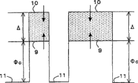
Fig. 1 (A) and 1 (B) are the schematic diagram of expression according to the transistorized structure of spin filtering of described embodiment, wherein Fig. 1 (A) is the profile of signal, and Fig. 1 (B) be structure shown in Fig. 1 (A) conduction band (or valence band) can be with schematic diagram, the spin direction of the spin energy band of barrier layer shown in the figure.When charge carrier was the hole, the spin direction on the band edge was consistent with the described direction of magnetization.When charge carrier was electronics, the spin direction on the band edge was opposite with the direction of magnetization.
As first, second and the 3rd non magnetic electrode layer 3,4 and 7, can use nonmagnetic metal, the non magnetic semiconductor of n-type or the non magnetic semiconductor of p-type.The thickness of the second non magnetic electrode layer 4 is preferably lower than the spin polarized hot carrier injected from the spin injector mean free path at the second non magnetic electrode layer 4.Base width is shorter than mean free path, is 0.5 or bigger so that allow the current delivery coefficient.Can obtain the electric current enlarging function.
As the first and second ferromagnetic barrier layers 2 and 6, can use insulation ferromagnetic semiconductor or ferromagnetic insulator.Being with by magnetic of ferromagnetic barrier layer exchanges mutual effect and spin-spin splitting.Can wherein only there be spin or has only the energy range of spinning down in formation on the described band edge.Spin polarized can being be called the spin energy band.The width of described energy range is called the spin-spin splitting width Delta.
Shown in Fig. 1 (B), indicate with the solid line of arrow ↑ expression of pointing to ferromagnetic barrier layer 2 and 6 and wherein can have the band edge that spins, that is to say last spin energy belt edge 9.Wherein can there be the band edge of spin down in solid line sign with arrow ↓ expression of pointing to ferromagnetic barrier layer 2 and 6, that is to say following spin energy belt edge 10.Last spin energy belt edge 9 among Fig. 1 (B) and the part between the following spin energy belt edge 10 are wherein only there to be the zone of spin.Its energy is higher than down, and the zone of spin energy belt edge 10 is wherein to go up the zone that spin and following spin can exist.The spin energy band of spin is lower than the situation of the spin energy band of spin down in Fig. 1 (B) expression.Opposite state also is possible.
The first ferromagnetic barrier layer 2 has such thickness, make and wherein can pass through such as tunnel effects such as Fowler-Nordheim tunnel (hereinafter referred to as the FN tunnel) or direct tunnels, by putting on the voltage of the first non magnetic electrode layer 3 and the second non magnetic electrode layer 4, charge carrier is transported to the second non magnetic electrode layer 4 from the first non magnetic electrode layer 3.Directly the tunnel is meant a kind of like this phenomenon, and wherein charge carrier directly passes thin potential barrier conveying.The FN tunnel is meant a kind of like this phenomenon, wherein certain below the applied voltage directly tunnel current of causing of tunnel can ignore, and charge carrier passes the triangle electromotive force on the potential barrier top that produces by applying certain voltage more than the numerical value by tunnel effect.
The voltage that puts on the first non magnetic electrode layer 3 and the second non magnetic electrode layer 4 can be the voltage range that is used for typical memory circuitry, for example, is approximately the hundreds of millivolt to several volts.The thickness on the second ferromagnetic barrier layer 6 must be such thickness, makes the thermal release of charge carrier and the electric current that is caused by described tunnel (so-called leakage current) not to occur from second non magnetic electrode layer 4 to the 3rd non magnetic electrode layers 7.
Non magnetic electrode layer 3,4 and 7 and ferromagnetic electrode layer 2 and 6 form the band structure shown in Fig. 1 (B).The solid line 11 of non magnetic electrode layer part shows the energy (top of valence band) of Fermi energy, the semi-conductive Fermi energy of n-type (p-type) or the conduction band bottom of metal among Fig. 1 (B).Ferromagnetic barrier layer 2 and the 6 lower energy barrier 5 usefulness Φ c to non magnetic electrode layer solid line 11 partly represent, and the spin-spin splitting width is represented with Δ.Ferromagnetic barrier layer 2 and 6 can have different Φ c and Δ.The situation that ferromagnetic barrier layer 2 and 6 has identical Φ c and Δ will be shown below.When charge carrier was electronics, nonmagnetic metal or n-N-type semiconductor N were used as non magnetic electrode layer 3,4 and 7, and did ferromagnetic barrier layer 2 and 6 with insulation ferromagnetic semiconductor or ferromagnetic insulator.In this case, ferromagnetic barrier layer 2 and 6 last spin energy belt edge 9 and following spin energy belt edge 10 are such spin energy belt edge: wherein the bottom of conduction band is spin-spin splitting.When charge carrier is the hole, makes non magnetic electrode layer 3,4 and 7 with the p-N-type semiconductor N, and do ferromagnetic barrier layer 2 and 6 with insulation ferromagnetic semiconductor or ferromagnetic insulator.In this case, ferromagnetic barrier layer 2 and 6 last spin energy belt edge 9 and following spin energy belt edge 10 are such spin energy belt edge, and wherein the top of valence band is spin-spin splitting.
Now will describe the transistorized operation principle of spin filtering in detail.In the following description, in order to simplify description, use the hot electron transistor mark simultaneously.The first non magnetic electrode layer 3 and the first ferromagnetic barrier layer 2 are called emitter 21.The second non magnetic electrode layer 4 is called base stage 22.The second ferromagnetic barrier layer 6 and the 3rd non magnetic electrode layer 7 are called collector electrode 23.The first non magnetic electrode layer 3 is called emitter 3.The 3rd non magnetic electrode layer 7 is called collector electrode 7.An example of the situation in the time of now will describing charge carrier and be electronics (operation principle is basic identical when charge carrier is the hole, is omitted so describe).
Fig. 2 (A) and 2 (B) can be with schematic diagram when applying the base earth bias voltage between according to the transistorized emitter of the spin filtering of described embodiment, base stage and collector electrode, the direction of magnetization situation parallel to each other on Fig. 2 (A) expression first and second ferromagnetic barrier layers wherein, and the direction of magnetization on Fig. 2 (B) expression first and second ferromagnetic barrier layers each other antiparallel and with the corresponding situation of Fig. 2 (A).Bias voltage V
EBBe applied between emitter 21 and the base stage 22.Bias voltage V
CBBe applied between base stage 22 and the collector electrode 23.V
EBAmplitude be set to satisfy (Φ c<qV
EB<Φ c+ Δ) equation relation.Q is the quantity of electric charge.
The transistorized collector electrode 23 of spin filtering selects to inject the spin polarized thermionic direction of base stage 22 as the spin analyzer.By bias voltage V
EBHeating is also injected the spin polarized hot electron 26 of base stage 22, because the width of base stage 22 is provided with to such an extent that be lower than the mean free path of spin polarized hot electron 26, so can be issued to the interface of base stage 22 and collector electrode 23 in the situation of off-energy not in trajectory mode (ballistically).In the second ferromagnetic barrier layer 6 of collector electrode 23, by two potential barriers of spin-spin splitting appearance of described conduction band with different barrier heights.Shown in Fig. 2 (A), when the direction of magnetization of the first and second ferromagnetic barrier layers 2 and 6 is parallel to each other, the last spin energy belt edge 9 on the second ferromagnetic barrier layer 6 that its spin is parallel with the spin of spin polarized hot electron 26, its energy is lower than spin polarized hot electron 26 energy.Spin polarized hot electron 26 is guided through the second ferromagnetic barrier layer 6, arrives collector electrode 7, becomes collector current I
C
Shown in Fig. 2 (B), during antiparallel, the spin polarized hot electron 27 with spin down injects base stages 22 each other for the first and second ferromagnetic barrier layers 2 and 6 the direction of magnetization.Have the following spin energy belt edge 10 on the second ferromagnetic barrier layer 6 of spin down, its energy is higher than the energy of described spin polarized hot electron 27.Described spin polarized hot electron 27 can not be by the conduction band on the second ferromagnetic barrier layer 6, the scattering (or backscattering) of generation and spin dependence on the interface of base stage 22 and collector electrode 23, and off-energy becomes base current I
B
Flow to the electric current of collector electrode from emitter, its current delivery coefficient depends on the relative direction of magnetization on the second ferromagnetic barrier layer 6 of the first ferromagnetic barrier layer 2 of emitter 22 and collector electrode 23 and is very different.In other words, collector current is very different to the current amplification factor of base current.
Fig. 3 (A) and 3 (B) are the schematic diagram of the static characteristic of expression during according to the spin filtering transistor base ground connection of described embodiment, wherein to the right the direction indication collector to-boase voltage V of trunnion axis in described figure
CB, and at its direction indication emitter base voltage V left
EB, and vertical axis is represented emitter current I
E, base current I
BWith collector current I
C, wherein the magnetized state between the ferromagnetic barrier layer of Fig. 3 (A) expression emitter and collector is the characteristic of parallel magnetized situation, and Fig. 3 (B) represents that it is the characteristic of the situation of antiparallel magnetization.In Fig. 3 (A) and 3 (B), α is the current delivery coefficient, and β is a current amplification factor, and subscript ↑ ↑ with ↓ ↑ parallel situation and their the antiparallel situations of the relative direction of magnetization on the ferromagnetic barrier layer of expression emitter and collector.
Shown in Fig. 3 (A), when the direction of magnetization of emitter and collector is parallel, most of emitter current I
ECan be collector current I
CShown in Fig. 3 (B), when direction of magnetization antiparallel, most of emitter current I
ECan become base current I
B, be similar to known hot electron transistor or bipolar transistor, can use base current I according to the transistor of described embodiment
BControl sets electrode current I
C, can be according to the relative direction of magnetization Control current amplification coefficient on the first and second ferromagnetic barrier layers.
As according to the transistorized ferromagnetic barrier layer of the spin filtering of described embodiment, can use such as EuS ferromagnetic semiconductors such as EuSe and EuO.Can also use ferromagnetic insulator such as (R represent rare earth element) such as R3Fe5O12.Can use namagnetic substance as non magnetic electrode layer.For example, can use with high density as impurity mix up such as metals such as Al or Au or such as non magnetic semiconductors such as Si or GaAs.Do ferromagnetic barrier layer with EuS, when making non magnetic electrode layer with A1, barrier height Φ c=1.4eV, and spin-spin splitting width Delta=0.36eV.According to described embodiment the spin filtering transistor can utilize above-mentioned material by known molecular beam epitaxial growth method, vacuum deposition method and sputtering method manufacturing.
The formal description with memory cell now utilizes the transistorized nonvolatile storage of spin filtering of the present invention.
Fig. 4 (A) is the schematic diagram of expression utilization according to the memory cell structure example of the spin filtering transistor 1 of described embodiment.In the memory cell shown in Fig. 4 (A), several spin filtering transistor arrangement become matrix, and emitter terminal E ground connection is so that be connected to readout bit line BL and sense word line WL to collector terminal C and base terminal B.Rewrite word line and rewrite bit line with other lead be on the spin filtering transistor, be arranged under the state of electric insulation intersected with each other.Can use readout bit line BL and sense word line WL as rewriteeing word line and rewriteeing bit line.Fig. 4 (A) is the schematic diagram of the cellular construction of described kind of situation of expression.Among Fig. 4 (A), memory cell can only constitute with the spin filtering transistor, and can have very simple wire structures.Can easily constitute and be applicable to superintegrated layout.Identical cellular construction is used for Fig. 4 (B).
Now with reference to the memory circuitry of Fig. 4 (B) description according to described embodiment.In memory circuitry 41 according to described embodiment, the second non magnetic electrode 4 is connected to word line 42 as the base stage of spin filtering transistor 1 (Fig. 1), the 3rd non magnetic electrode 7 is connected to bit line 43 as the collector electrode of spin filtering transistor 1, and bit line 43 is by load (R
L) 44 be connected to power supply (V
CC) 45, and the first non magnetic electrode 3 is as the grounded emitter of spin filtering transistor 1.Do load with pure resistance.Can use and utilize transistorized active load.
In order to read the designated memory cell canned data, select the word line of appointment, between emitter and base stage, apply bias voltage, apply the supply voltage V of power supply 45 to bit line 43 by load resistance 44
CC, according to the output voltage V that appears on the bit line 43
0Amplitude read canned data.Among Fig. 4 (C), vertical axis is represented collector current IC, and trunnion axis is represented collector emitter voltage V
CB, at the transistorized I of described spin filtering shown in the same figure
C-V
CEThe load straight line 46 of characteristic and load resistance 44.
Determine output voltage V according to these characteristic intersection points
0Shown in Fig. 4 (C), wherein the first and second ferromagnetic barrier layers 2 and 6 mutual magnetized state be parallel and antiparallel output voltage be Vo ↑ ↑ and Vo ↓ ↑.Vo ↑ ↑ and Vo ↓ ↑ absolute value and Vo ↑ ↑ and Vo ↓ ↑ ratio can pass through circuit parameter (R
LAnd Vcc) optimizes.Different with MTJ, under the situation of the structure of adjusting device not own, can obtain to have the ratio of the output signal and the output signal of necessary amplitude according to the Nonvolatile memory device of described embodiment.
The spin filtering effect that is used for according to the transistor of described embodiment is a kind of effect of utilizing the spin-spin splitting of ferromagnetic mass-energy band, and ability is selected in the spin with the TMR effect that is higher than MTJ.When the mean free path of base width being arranged to be lower than spin polarized hot carrier and the relative magnetized state between the first and second ferromagnetic barrier layers were parallel magnetization, the current delivery factor alpha was (by I
C/ I
EDefinition) can be 0.5 or higher.When it was antiparallel magnetization, the current delivery coefficient was very little.From currentamplificationfactor (by I
C/ I
BSee that definition) change of current delivery coefficient can also further be amplified under the situation of parallel magnetization and antiparallel magnetization.Above-mentioned peripheral circuit is optimized output signal at the huge spin filtering transistor output characteristic of magnetized state difference wherein.Can easily obtain required output signal absolute value and required output signal ratio.
A kind of non-volatile memory circuits of utilizing its output characteristic fixed transistor (hereinafter referred to as " spin transistor ") with the charge carrier spin direction now will be described.
Relate to a kind of non-volatile memory circuits of utilizing spin transistor according to memory circuitry of the present invention.Described spin transistor comprises such as ferromagnetic materials such as feeromagnetic metal and ferromagnetic semiconductors, and according to the spin direction of magnetized state control charge carrier, so that change described output characteristic.According to magnetized state stored information in described spin transistor of ferromagnetic material, utilize the transistor output characteristic of reflection magnetized state to read described information.A nonvolatile memory cell can constitute with a spin transistor.Can optimize numerical value by the peripheral circuit that is connected to described memory cell about the output signal of described stored information.
In more detail, described spin transistor have can by magnetic field control independently at least one ferromagnetic layer (free layer) of the direction of magnetization and wherein the direction of magnetization be fix or its coercive force greater than coercitive at least one ferromagnetic layer (fixed bed) of free layer, and described spin transistor be a kind of can be under identical biasing according to the transistor of the relative direction of magnetization oxide-semiconductor control transistors output characteristic of free layer and fixed bed.Change the direction of magnetization of free layer by magnetic field.The relative magnetized state of free layer and fixed bed can be two kinds of magnetized states of parallel magnetization and antiparallel magnetization.Two kinds of magnetized states are corresponding to the binary message of storing.
Spin transistor can according to obtain such as the electric conduction phenomena that changes with the spin direction of stream with scattering, tunneling magnetoresistance and the spin filtering effect etc. of spin dependence with described transistor in the corresponding output characteristic of magnetized state.Spin transistor has first electrode structure that injects spin-poarized charge carriers, second electrode structure that receives spin-poarized charge carriers and control are conducting to the spin-poarized charge carriers quantity of second electrode structure from first electrode structure third electrode structure.
Spin transistor is based on the operation principle work identical with typical transistors, exception be that electric conduction phenomena depends on spin.Spin transistor can be categorized as such as the current drives transistor npn npn of bipolar transistor etc. or such as the driven transistor npn npn of field-effect transistor etc.In the current drives transistor npn npn, first electrode structure is corresponding to emitter, and second electrode structure is corresponding to collector electrode, and the third electrode structure is corresponding to base stage.The spin filtering transistor of describing in described embodiment is categorized as current drive-type.In the driven transistor npn npn, first electrode structure is corresponding to source electrode, and second electrode structure is corresponding to drain electrode, and the third electrode structure is corresponding to grid.Under identical biasing, the output current in spin transistor (collector current or drain current) changes according to the magnetized state that is included in the ferromagnetic material in the described spin transistor.
The details of described spin transistor now will be described.To spin transistor and a kind of typical output characteristic of utilizing the nonvolatile storage of spin transistor be described.Can utilize the magnetic field that is applied to the free layer in the spin transistor to realize the parallel magnetization or the antiparallel magnetization of the relative magnetized state of free layer and fixed bed.Magnetized state can stably exist, and is higher than the coercitive magnetic field of free layer unless applied one.
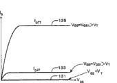
Fig. 5 (A) schematically represents the example of the output characteristic of current drive-type spin transistor.Be similar to the driving transistor of exemplary currents, can be according to base current I
BAmplitude come control sets electrode current I
CThe amplitude of collector current depends on the magnetized state that is included in the ferromagnetic material in the described spin transistor.Among Fig. 5 (A), when apply identical biasing (I to described spin transistor
B=I
B1), collector current I during parallel magnetization
C ↑ ↑Greatly, collector current I during antiparallel magnetization
C ↓ ↑Little.
Fig. 5 (B) schematically represents an example of voltage driven type spin transistor output characteristic.Be similar to such as field-effect transistors such as typical MOS transistor, as grid-source voltage (V
GS) less than threshold value V
T(V
GS<V
T) time, spin transistor is in nonconducting state, so produce drain current hardly.Apply and be higher than V
TV
GSThe time, described spin transistor just enters conducting state.At identical biasing (V
GS=V
GS1) under, when the ferromagnetic material in being included in described spin transistor has parallel magnetization or antiparallel magnetization, drain current value difference.Among Fig. 3 (B), has under the parallel magnetized situation drain current I
D ↑ ↑Has under the situation of antiparallel magnetization drain current I greatly,
D ↓ ↑Little.
Spin transistor can detect the relative direction of magnetization that is included in free layer and fixed bed in described current drive-type and the voltage driven type device according to the amplitude of collector current or drain current on electric.As above-described, ferromagnetic material can stably keep its direction of magnetization, is higher than the coercitive magnetic field of described free layer unless apply one from the outside.Spin transistor can be parallel magnetized or antiparallel magnetization by allowing to be included in the free layer in the described device and the relative magnetized state of fixed bed, stores binary message in non-volatile mode.A nonvolatile memory cell can constitute with a spin transistor.
Be example now, describe the nonvolatile storage that utilizes spin transistor in detail in order to situation with the voltage driven type spin transistor.Utilize the current drive-type spin transistor can constitute in a like fashion as the nonvolatile storage of memory cell.
Fig. 6 (A) is the schematic diagram that expression utilizes the memory cell structure example of spin transistor, and Fig. 6 (B) is the schematic diagram of expression based on the memory circuitry structure example of described memory cell.The relation of Fig. 6 (A) and 6 (B) is identical with the relation of Fig. 4 (A) and 4 (B).In the memory cell shown in Fig. 6 (A), several spin transistors 150 are arranged in matrix, and source S ground connection is so that be connected to readout bit line BL and sense word line WL to drain D and grid G respectively.Rewrite word line and rewrite bit line on described spin transistor 150, be arranged in intersected with each other, be in electric go up and the state of other wire insulation under.Can use readout bit line BL and sense word line WL as rewriteeing word line and rewriteeing bit line.Fig. 6 (A) and 6 (B) are the structural representations of the described situation of expression.In Fig. 6 (A) and 6 (B), memory cell can constitute with a spin transistor also can have very easy wire structures.
Specifically, in the voltage driven type spin transistor of the form with the MOS transistor of being similar to, source electrode is shared between consecutive storage unit.Can easily constitute and be suitable for micro-machined layout.
Rewriting/readout bit line and rewriting/sense word line abbreviate bit line BL and word line WL as.
The method of rewrite information is as follows: make electric current flow to bit line BL and the word line WL that intersects on selected memory cell, make the free layer reversing of described selected memory cell so that utilize by flowing to the resultant magnetic field of the current-induced of lead separately.In this case, be connected to and selected unit same bit lines BL or the non-selected unit on word line WL magnetic reversal not in order to make, to be provided with like this and flow to the current value of lead separately, make the magnetization reversing does not take place in the magnetic field that causes by one of described each lead.
When reading information, apply voltage,, detect the amplitude of drain current so that described spin transistor conducting applies voltage to described bit line then to the word line WL that is connected to selected unit.According to the amplitude of described drain current, can detect the relative magnetized state of free layer and fixed bed.
Fig. 6 (B) is a memory circuitry, and it is connected to output end vo and is branched off into the source voltage V of memory circuitry bit line one end shown in Fig. 6 (A) from output end vo by load
DDThe static characteristic and the working point of the memory cell shown in Fig. 6 (C) presentation graphs 6 (B).Here, use the active load 160 that forms by inhibition type (depression type) MOS transistor as load.Shown in Fig. 4 (B), can use pure resistance.Shown in Fig. 6 (C), on the grid of spin transistor 150, apply grid voltage V when reading information
GS, so that by described load source voltage V
DDBe applied on the bit line BL, move on the load curve in Fig. 6 (C) (p11 and p12 among the figure) according to the magnetized state of fixed bed and free layer the working point of active load.Output signal Vo when parallel magnetization and antiparallel magnetization is the V among the figure
O ↑ ↑And V
O ↓ ↑The absolute value of output signal and (V separately
0 ↑ ↑/ V
O ↓ ↑) ratio can be with the parameter of the transistor characteristic of active load and peripheral circuit such as V
DDOptimize.For example, optimize the intersection point of the load curve of the static characteristic of described spin transistor and active load.As drain current ratio I
0 ↑ ↑/ I
O ↓ ↑Hour, can obtain big output signal ratio.When memory cell changes I
0 ↑ ↑And I
O ↓ ↑Numerical value, and the saturation current of active load is greater than I
O ↓ ↑And less than I
0 ↑ ↑The time, output voltage almost can't change.Because do not use sense amplifier to read information, may read at a high speed.Described memory circuitry has the following advantages: can obtain the output signal of required amplitude easily, and may read at a high speed.
In the memory cell of utilizing prior art MTJ and MOS transistor, read output voltage with sense amplifier according to the resistance of MTJ.Output voltage is determined by the impedance (junction resistance) of current value that flows to MTJ and MTJ.The output voltage ratio can not freely be adjusted with peripheral circuit.
The spin transistor structure that can be applied to according to the non-volatile memory circuits of described embodiment is now described with reference to the accompanying drawings.FM is metallic ferromagnetic abbreviation, and FS is the abbreviation of conduction ferromagnetic semiconductor, and IFS is the abbreviation of insulation ferromagnetic semiconductor, and NM is the abbreviation of namagnetic substance.The NM metal is represented nonmagnetic metal, and the NM semiconductor is represented non magnetic semiconductor.Now the current drive-type spin transistor will be described.
Fig. 7 be hot electron transistor type spin transistor can be with schematic diagram.Spin transistor 200 has emitter 201 and the base stage of being made by FM or FS 205.In more detail, spin transistor 200 have the emitter 201 made by FM (or FS), the emitter barrier 203 made by NM, the base stage of making by FM (or FS) 205, the collector electrode barrier layer 207 of making by NM and the collector electrode of making by NM 211.Can use nonmagnetic metal or non magnetic semiconductor as NM.
In spin transistor shown in Figure 7 200, spin polarized hot carrier is injected base stage 205 from emitter 201 by emitter barrier 203 tunnels.
When emitter 201 had parallel magnetization with base stage 205, scattering with spin dependence took place in base stage 205 in the spin polarized hot carrier of injection hardly.Make that when base width is set so spin polarized hot carrier can be by the trajectory mode by base stage 205 carry the time, they pass collector electrode barrier layer 207 arrival collector electrodes 211.Carry out the transistor operation identical with the typical heat electron transistor.
When emitter 201 and base stage 205 have antiparallel magnetization, from emitter 201 inject base stages 205 spin polarized hot carrier since base stage 205 with the scattering of spin dependence off-energy, become base current, do not pass collector electrode barrier layer 207.When emitter 201 and base stage 205 have antiparallel magnetization, the current delivery coefficient ratio both to have parallel magnetized situation low.When spin transistor 200 applied identical biasing, the difference on the relative magnetized state of emitter 201 and base stage 205 made current delivery coefficient or current amplification factor different.The barrier height on choice set electrode barrier layer suitably, spin transistor 200 can at room temperature be worked.
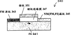
Fig. 8 utilizes thermal release can be with schematic diagram as the hot electron transistor type spin transistor that injects mechanism to base stage spin.As shown in Figure 8, spin transistor 220 have the emitter 221 made by FM (or FS), the base stage 225 made by FM (or FS) and be arranged between the two the emitter barrier of making by NM 223.The collector electrode 231 that it also has the collector electrode barrier layer 227 that formed by NM and is formed by NM in the opposite side of the knot of base stage 225 and emitter barrier 223.Can be non magnetic semiconductor as emitter barrier 223 and collector electrode barrier layer 227.Can be used as collector electrode 231 to non magnetic semiconductor or nonmagnetic metal.
Between emitter 221 and emitter barrier 223, form ohmic contact or tunnel contact.Forming knot between base stage 225 and the emitter barrier 223 or between base stage 225 and the collector electrode barrier layer 227, can be with discontinuity shown in Fig. 9 so that have.Can realize by the heterojunction of the knot of the Schottky between NM semiconductor and the FM and NM semiconductor and FS with discontinuity.Perhaps, form Schottky knot by FS and FM, the Schottky potential barrier of Chan Shenging is an emitter barrier in this case, and FS is an emitter and FM is a base stage.
By applying biasing to base stage 225, make the spin-poarized charge carriers that is diffused into emitter barrier 223 from emitter 221 inject base stage 225 as hot carrier by thermal release with respect to emitter 221.When emitter 221 had parallel magnetization with base stage 225, the spin-poarized charge carriers that injects base stage 225 arrived at collector electrode under situation about not taking place with the scattering of spin dependence.When emitter 221 and base stage 225 had antiparallel magnetization, spin-poarized charge carriers became base current by the scattering with spin dependence.Spin transistor 220 utilizes in the base stage and scattering spin dependence.Be similar to spin transistor 200, under parallel magnetization and antiparallel magnetization, have the relation of weighing the advantages and disadvantages in the ratio of the current delivery factor and the parallel magnetization between the current delivery coefficient.Compare with the spin transistor that utilizes the tunnel to inject, have such specific character, that is, current driving capability can be greatly and is realized working and room temperature easily.
Fig. 9 be utilize the spin filtering effect hot electron transistor type spin transistor can be with schematic diagram.Though described in detail, also will describe its characteristic now tout court.Spin transistor 240 shown in Fig. 9 has the emitter barrier 243 and the collector electrode barrier layer 247 of being made by IFS.The charge carrier that only has the spin that the spin filtering effect of emitter barrier 243 causes, just the emitter 241 that can make from NM semiconductor (or NM metal) optionally injects the base stage 245 that NM semiconductor (or NM metal) is made.Base width is arranged to be lower than the mean free path of spin polarized hot carrier.Inject the spin polarized hot carrier of base stage 245 and pass through base stage 245 conductings in the trajectory mode.At this moment, provide such biasing to spin transistor 240, the energy that makes spin polarized hot carrier inject the last spin energy band on collector electrode barrier layer 247 (the spin energy belt edge of representing to upward arrow with Fig. 9) divides width and following spin energy band (the spin energy belt edge that the downward arrow of Fig. 9 is represented).When emitter barrier 243 has parallel magnetization with collector electrode barrier layer 247, inject the low-energy spin energy band of spin polarized hot carrier with collector electrode barrier layer 247 of base stage 245, spin filtering effect by collector electrode barrier layer 247 is passed described potential barrier, and can propagate into the collector electrode 251 of NM semiconductor (or NM metal).When emitter barrier 243 and collector electrode barrier layer 247 had antiparallel magnetization, most of spin polarized hot carrier can not lean on the spin filtering effect on collector electrode barrier layer 247 to pass collector electrode barrier layer 247, becomes base current.
In spin transistor 240, current delivery coefficient (or current amplification factor) is different according to the relative direction of magnetization on emitter barrier 243 and collector electrode barrier layer 247.The spin filtering effect has very big spin and selects ability.In described transistor, the ratio of the current delivery factor when parallel magnetization and antiparallel magnetization increases.Spin transistor 240 can reduce base width fully.Spin transistors with scattering spin dependence shown in Fig. 7 and 8 are different with utilizing, and following advantage is arranged: select between the ability there is not the relation of weighing the advantages and disadvantages in base width at current amplification factor and spin.
Figure 10 be tunnel grounded base transistor type spin transistor can be with schematic diagram.As shown in figure 10, in tunnel grounded base transistor type spin transistor 260, p-type (or n-type) FS is as emitter 261 and collector electrode 265, and n-type (or p-type) NM semiconductor is as tunnel base stage 263.Preferably use II type heterojunction, make base stage 263 be between emitter and the base stage and between base stage and collector electrode to the potential barrier of hole (or electronics).Base width is less, so that produce the tunnel current from the emitter to the collector electrode.
In the structure shown in Figure 10, when emitter 261 had parallel magnetization with collector electrode 265, the charge carrier with some spins of emitter can easily pass through tunnel and arrive collector electrode 265, and tunneling conductance rate height.When emitter 261 and collector electrode 265 have antiparallel magnetization, because tunnel magneto-resistance effect (TMR effect) tunneling conductance electricity rate is low.The amplitude of collector current can be according to the relative magnetized state control of emitter 261 and collector electrode 265.
When the TMR ratio in the spin transistor 260 is big, depend on that the variation of collector current of the magnetized state of emitter and collector can increase.In order to present the TMR effect by spin transistor 260 effectively,, suppress layer and preferably do not expand to the collector electrode side when when base-collector junction applies reverse bias.When the inhibition layer expands to the base stage side, on the saturation characteristic of collector current, there is the possibility that goes wrong.
When base layer is mixed up with high density, make in the spin transistor 260 the inhibition layer not broadening to base layer, and the inhibition layer of base-collector junction is when expanding to the collector electrode side, and the charge carrier that can not expect the TMR effect in the base stage and inject collector electrode has a resistance with scattering spin dependence by collector electrode.Utilization can change the amplitude of collector current according to the magnetized state of emitter and collector with the scattering of spin dependence.The resistance variations that causes with the scattering of spin dependence is little.Compare with utilizing the TMR effect, effect may be not high.The voltage driven type spin transistor is now described with reference to the accompanying drawings.
Figure 11 is the schematic diagram of the cross-section structure of expression MOS transistor type spin transistor.As shown in figure 11, MOS transistor type spin transistor 300 has a kind of like this structure, and wherein source electrode 303 is made by FM, and drain electrode 305 is made by FM, and grid 311 forms on NM semiconductor 301 by gate insulating film 307.Tie as source electrode 303 and drain electrode 305 with FM and the semi-conductive Schottky of NM.Other structure is identical with typical MOS transistor.
The spin-poarized charge carriers that injects the raceway groove that directly forms from source electrode 303 below NM semiconductor 301 gate insulating films 307 passes raceway groove and arrives drain electrode 305 (below ignoring for the sake of simplicity, the influence of the Rashba effect that the grid electric field of the spin of injecting described raceway groove causes).When source electrode 303 had parallel magnetization with drain electrode 305, the scattering with spin dependence did not take place in the spin-poarized charge carriers of injection drain electrode 305.When they have antiparallel magnetization, the resistance that the scattering of generation and spin dependence causes in drain electrode 305.
In transistor 300, mutual conductance is according to the source electrode and the drain electrode relative direction of magnetization and different.
FS can also be as source electrode 303 and drain electrode 305, forms the pn knot between it and semiconductor 301, to form source electrode and drain electrode.
Figure 12 is the schematic diagram that the expression modulation mixes up the cross-section structure of transistor-type spin transistor.Spin transistor 320 has: the source electrode of being made by FM (or FS) 323 that is connected to the two-dimentional carrier gases that produces on the interface of a NM semiconductor 321 and the 2nd NM semiconductor 327; The drain electrode 325 of making by FM (or FS); And grid 331.To mix up transistor identical with typical modulation for this, and just source electrode 323 and drain electrode 325 are made by ferromagnetic material.
Spin-poarized charge carriers injects the raceway groove 333 that is formed by two-dimentional carrier gases from source electrode 323.Because with the cause of the scattering of spin dependence, the spin-poarized charge carriers that reaches drain electrode 325 and drain 325 the relative direction of magnetization and has different mutual conductances according to source electrode 323 in the drain electrode 325.
Figure 13 utilizes the profile of FS as the MOS transistor type spin transistor of channel region.Spin transistor 340 shown in Figure 13 has a kind of like this structure, wherein drain electrode 345 and the grid 351 that forms the source electrode 343 made by FM on FS 341, made by NM (or FM or FS) by gate insulating film 347.The Schottky knot of FM and FS is as source electrode 343.Other structure is identical with typical MOS transistor.
Spin-poarized charge carriers injects raceway groove 341 from source electrode 343 by Schottky potential barrier tunnel.TMR effect of injecting by the tunnel and the raceway groove of FS 341 and the scattering of spin dependence realize depending on the mutual conductance of the relative direction of magnetization of source electrode 343 and FS341.
The spin transistor 360 of its cross-section structure shown in Figure 14 is a kind ofly to have the tunnel junction structure between the drain electrode 363 that is inserted in the source electrode 361 made by FM (FS) and is made by FM (or FS) and grid 371 is set like this so that apply the spin transistor of electric field to tunnel barrier layer 365.
The film thickness of tunnel barrier layer 365 preferably is set like this, makes Fowler-Nordheim (FN) tunnel does not take place when only applying biasing between source electrode and drain electrode.Change the triangle electromotive force that between source electrode and drain electrode, applying the tunnel barrier band edge that produces of biasing by grid voltage, so that induce the FN tunnel, the acquisition drain current.
Spin-poarized charge carriers scattering of generation and spin dependence in drain electrode 363 from source electrode 361 injections according to the relative magnetized state of source electrode 361 and drain electrode 363.Can control described transistorized mutual conductance by the relative direction of magnetization of source electrode and drain electrode.
A kind of tunnel barrier layer of being made by IFS 385 of spin transistor 380 usefulness of its cross-section structure shown in Figure 15 replaces the tunnel barrier layer of the spin transistor 360 shown in Figure 14.Source electrode 381 must be made by FM or FS.Drain electrode 383 needs not to be ferromagnetic material.The barrier height of IFS tunnel barrier layer 385 is different according to the spin direction of charge carrier.When source electrode 381 has parallel magnetization with tunnel barrier layer 385, source electrode and the drain electrode between and apply biasing between source electrode and the grid, make transistor enter conducting state.Under identical bias condition, when source electrode 381 and tunnel barrier layer 385 had antiparallel magnetization, the height of the tunnel barrier of seeing from some spins of source electrode 381 had increased.The tunnelling probability of spin-poarized charge carriers reduces, and drain current is reduced.The spin of spin filtering effect selects ability very big.When utilizing a kind of ferromagnetic material with big spin polarized rate as source electrode 381, mutual conductance can change a lot according to the relative direction of magnetization of source electrode and drain electrode.
Above-mentioned different spin transistor can be as the memory cell of Fig. 4 or memory circuitry shown in Figure 6.
Also might form a kind of structure, wherein the source electrode of the voltage driven type spin transistor shown in two Figure 11,14 and 15 is shared as a source electrode.Figure 16 (A) is the schematic diagram of structure example that expression has the memory cell of shared source configuration.Figure 16 (B) is the schematic diagram of cross-section structure example that expression has the memory cell of shared source configuration.
Memory cell structure shown in Figure 16 (A) and 16 (B) has: the first spin transistor Tr1 adjacent one another are and the second spin transistor Tr2; The word line WL that can connect the grid G 2 of the grid G 1 of the first spin transistor Tr1 and the second spin transistor Tr2 sharedly; Be connected to the first bit line BL1 of first drain D 1 of the first spin transistor Tr1; Be connected to the second bit line BL2 of second drain D 2 of second spin transistor; The ferromagnetic source S of between the first and second spin transistor Tr1 and Tr2, sharing; And with the lead of its ground connection.Utilize the structure of above-mentioned shared source electrode that a kind of superintegrated cellular construction that is suitable for is provided.
For in the voltage driven type spin transistor shown in Figure 11,14 and 15, it is minimum that the leakage current when non-conduction is reduced to, and preferably uses the SOI substrate with high-insulativity shown in Figure 16 (B).
As mentioned above, according to the spin filtering transistor of embodiment of the present invention and the different spin transistors shown in the described embodiment have a kind of can be according to the characteristic of the relative direction of magnetization control output characteristic that is included in fixed bed in the described device and free layer.Described relative magnetized state has non-volatile characteristic, can keep its state under the situation that does not apply power supply.Described relative magnetized state can be stored binary message in non-volatile mode.Utilize above-mentioned output characteristic on electric, to detect described relative magnetized state.A nonvolatile memory cell can constitute with a spin transistor.Utilize described non-volatile memory circuits, utilize spin transistor, can freely design the amplitude of output signal and output signal ratio stored information according to described embodiment.
Utilization can improve the operating rate and the integrated level of non-volatile memory circuits according to the spin transistor and the memory circuitry that utilizes described kind of spin transistor of embodiment of the present invention.
By some embodiment the present invention has been described above.The invention is not restricted to this.For the professional and technical personnel, obviously can realize various modification, improvement and combination.
The possibility of commercial Application
As mentioned above, can be according to ferromagnetic barrier layer according to spin filtering transistor of the present invention The relative direction of magnetization greatly change output characteristics.
Utilize spin filtering transistor and another to have the spin crystal of the characteristic identical with it Pipe can be according to being included in the described transistor as the non-volatile memory circuits of memory cell The relative direction of magnetization storage binary message of ferromagnetic material, and can be in electric detection The described relative direction of magnetization. Utilize non-volatile memory circuits of the present invention freely to establish Meter is with respect to the output signal of described canned data. Can realize crystal of a kind of usefulness Pipe consists of a nonvolatile memory cell with superintegrated high speed nonvolatile storage electricity The road.
Claims (18)
1. transistor, the base stage that it comprises the emitter made by ferromagnetic material, made by ferromagnetic material, the collector electrode of making by namagnetic substance or ferromagnetic material, be arranged on first barrier layer between described emitter and the described base stage and make second barrier layer that is arranged between described base stage and the described collector electrode by namagnetic substance by what namagnetic substance was made
Wherein spin-poarized charge carriers is passed through the Fowle-Nordheim tunnel effect, inject described base stage from described emitter; And
The barrier height on described second barrier layer can make described spin-poarized charge carriers can be transmitted by described barrier height when described emitter has parallel magnetization with described base stage and can not be transmitted by described barrier height when described emitter and described base stage have antiparallel magnetization.
2. transistor as claimed in claim 1, wherein said emitter and described base stage are made by feeromagnetic metal or ferromagnetic semiconductor.
3. transistor as claimed in claim 1, wherein said emitter and described base stage are formed by ferromagnetic semiconductor, and described first barrier layer and described second barrier layer are formed by semiconductor.
4. transistor as claimed in claim 1 is wherein adjusted the barrier height on described first barrier layer and second barrier layer so that allow working and room temperature.
5. transistor as claimed in claim 1, wherein the described charge carrier that injects described base stage from described emitter depends on the relative direction of magnetization of described emitter and described base stage with respect to the current delivery coefficient of described collector electrode.
6. transistor, the base stage that it comprises the emitter made by ferromagnetic material, made by ferromagnetic material, the collector electrode of making by namagnetic substance or ferromagnetic material, be arranged on first barrier layer of making by nonmagnetic substance between described emitter and the described base stage, be arranged on second barrier layer of making by nonmagnetic substance between described base stage and the described collector electrode
Wherein spin-poarized charge carriers injects described base stage by thermionic emission from described emitter.
7. transistor as claimed in claim 6, wherein said emitter and described base stage by feeromagnetic metal or or ferromagnetic semiconductor make, and described first barrier layer and second barrier layer are made by semiconductor.
8. transistor as claimed in claim 6 wherein utilizes the contact of ohmic contact or tunnel to form described emitter and described first barrier layer.
9. transistor as claimed in claim 6, wherein when described base stage is feeromagnetic metal, the barrier structure on described base stage and described first barrier layer is formed by the Shottky knot, and when described base stage was ferromagnetic semiconductor, the barrier structure on described base stage and described first barrier layer formed according to the discontinuity of being with on described base stage and described first barrier layer.
10. transistor as claimed in claim 6, wherein when described base stage is feeromagnetic metal, the barrier structure on described base stage and described second barrier layer forms by the Schottky knot, and when described base stage was ferromagnetic semiconductor, the barrier structure on described base stage and described second barrier layer formed according to the discontinuity of being with on described base stage and described second barrier layer.
11. transistor as claimed in claim 6, wherein said emitter is made by ferromagnetic semiconductor, and described base stage is made by feeromagnetic metal, and described first barrier layer is formed by the Schottky potential barrier that is formed between ferromagnetic semiconductor and the feeromagnetic metal.
12. transistor as claimed in claim 6, wherein the charge carrier that injects described base stage from described emitter depends on the relative direction of magnetization of described emitter and described base stage with respect to the current delivery coefficient of described collector electrode.
13. a transistor, it comprises the emitter made by the ferromagnetic semiconductor of first conduction type, the collector electrode of being made by the ferromagnetic semiconductor of first conduction type and the base stage of being made by the ferromagnetic semiconductor of second conduction type that is different from first conduction type,
Wherein adjust the width of described base stage like this, so that form tunnel from described emitter to described collector electrode; And
Can control the mutual conductance or the amplitude of output current according to the relative direction of magnetization of described emitter and described collector electrode.
14. transistor as claimed in claim 13, wherein said base stage is the tunnel barrier layer for the majority carrier of described emitter and described collector electrode, and the bottom of the conduction band in the described base stage is lower than the top of the valence band in the described collector electrode, makes that described emitter and described collector electrode are the energy barriers for the majority carrier of described base stage.
15. a storage device, it comprises:
According to any one a transistor in the claim 1 to 14;
The information rewriting device is used for rewriteeing information in the described transistor by the magnetized state that change is included in the described ferromagnetic material of described transistor; And
Information read device is used for reading form canned data with magnetized state from described transistorized output characteristic.
16. storage device as claimed in claim 15, wherein have the free layer of the ferromagnetic material that can control the direction of magnetization independently and do not change the fixed bed of the ferromagnetic material of the direction of magnetization, and described transistor can keep wherein said free layer and described fixed bed to have second state that first state of the identical direction of magnetization and wherein said free layer and described fixed bed have the different direction of magnetizations according to any one transistor in the claim 1 to 14.
17. storage device, wherein have the free layer of the ferromagnetic material that can control the direction of magnetization independently and do not change the fixed bed of the ferromagnetic material of the direction of magnetization according to any one transistor in the claim 1 to 14, and in order to relative direction of magnetization stored information, so that according to the described transistorized information of output characteristic detection of stored in described transistor that depends on the relative direction of magnetization of described fixed bed and described free layer according to described fixed bed and described free layer.
18. a storage device, it comprises:
According to an any one transistor in the claim 1 to 14;
Be connected to first lead of described emitter;
Be connected to second lead of described base stage; And
Be connected to described collector electrode privates.
Applications Claiming Priority (4)
| Application Number | Priority Date | Filing Date | Title |
|---|---|---|---|
| JP217336/2002 | 2002-07-25 | ||
| JP2002217336 | 2002-07-25 | ||
| JP2003086145A JP4477305B2 (en) | 2002-07-25 | 2003-03-26 | Spin transistor and nonvolatile memory using the same |
| JP86145/2003 | 2003-03-26 |
Related Child Applications (1)
| Application Number | Title | Priority Date | Filing Date |
|---|---|---|---|
| CN2007101696922A Division CN101202302B (en) | 2002-07-25 | 2003-07-25 | Spin transistor based on the spin-filter effect, and non-volatile memory using spin transistors |
Publications (2)
| Publication Number | Publication Date |
|---|---|
| CN1685526A CN1685526A (en) | 2005-10-19 |
| CN100470844C true CN100470844C (en) | 2009-03-18 |
Family
ID=31190300
Family Applications (1)
| Application Number | Title | Priority Date | Filing Date |
|---|---|---|---|
| CNB038224801A Expired - Fee Related CN100470844C (en) | 2002-07-25 | 2003-07-25 | Spin transistor using spin filter effect and nonvolatile memory using spin transistor |
Country Status (8)
| Country | Link |
|---|---|
| US (4) | US7423327B2 (en) |
| EP (1) | EP1555694B1 (en) |
| JP (1) | JP4477305B2 (en) |
| KR (1) | KR100977829B1 (en) |
| CN (1) | CN100470844C (en) |
| AU (1) | AU2003252691A1 (en) |
| TW (1) | TWI310184B (en) |
| WO (1) | WO2004012272A1 (en) |
Families Citing this family (33)
| Publication number | Priority date | Publication date | Assignee | Title |
|---|---|---|---|---|
| WO2004079827A1 (en) * | 2003-03-07 | 2004-09-16 | Japan Science And Technology Agency | Field-effect transistor with spin-dependent transmission characteristic and nonvolatile memory using same |
| JP4212397B2 (en) | 2003-03-28 | 2009-01-21 | 株式会社東芝 | Magnetic memory and writing method thereof |
| EP1610386A4 (en) * | 2003-03-31 | 2009-04-01 | Japan Science & Tech Agency | Tunnel transistor having spin-dependent transfer characteristic and nonvolatile memory using same |
| US7045368B2 (en) * | 2004-05-19 | 2006-05-16 | Headway Technologies, Inc. | MRAM cell structure and method of fabrication |
| US7411235B2 (en) | 2004-06-16 | 2008-08-12 | Kabushiki Kaisha Toshiba | Spin transistor, programmable logic circuit, and magnetic memory |
| JP2006237304A (en) * | 2005-02-25 | 2006-09-07 | Osaka Industrial Promotion Organization | Ferromagnetic conductor material, its manufacturing method, magnetoresistive element and field effect transistor |
| EP1705665B1 (en) * | 2005-03-24 | 2008-04-02 | Hitachi Ltd. | Conduction control device |
| JP5030397B2 (en) * | 2005-06-24 | 2012-09-19 | 日本電信電話株式会社 | Spin transistor |
| US7372674B2 (en) * | 2005-07-22 | 2008-05-13 | Hitachi Global Storage Technologies Netherlands B.V. | Magnetic tunnel transistor with high magnetocurrent and stronger pinning |
| US7646627B2 (en) | 2006-05-18 | 2010-01-12 | Renesas Technology Corp. | Magnetic random access memory having improved read disturb suppression and thermal disturbance resistance |
| JP4883982B2 (en) | 2005-10-19 | 2012-02-22 | ルネサスエレクトロニクス株式会社 | Nonvolatile memory device |
| JP4693634B2 (en) * | 2006-01-17 | 2011-06-01 | 株式会社東芝 | Spin FET |
| JP2008047706A (en) | 2006-08-16 | 2008-02-28 | Nec Lcd Technologies Ltd | Semiconductor circuit, and semiconductor device using it |
| JP4455558B2 (en) * | 2006-09-08 | 2010-04-21 | 株式会社東芝 | Spin MOSFET |
| JP5157268B2 (en) * | 2007-06-13 | 2013-03-06 | 株式会社日立製作所 | Spin accumulation magnetization reversal type memory device and spin RAM |
| KR100862216B1 (en) * | 2007-08-02 | 2008-10-09 | 한국과학기술원 | The nonvolatile dram having capacitorless dram characteristic and nonvolatile memory characteristic by resistance switching material |
| JP2009064826A (en) | 2007-09-04 | 2009-03-26 | Tdk Corp | Spin transistor and its manufacturing method |
| US7936028B2 (en) | 2007-11-09 | 2011-05-03 | Samsung Electronics Co., Ltd. | Spin field effect transistor using half metal and method of manufacturing the same |
| US20090141409A1 (en) * | 2007-12-03 | 2009-06-04 | Santos Tiffany S | Spin filter spintronic devices |
| US8659852B2 (en) * | 2008-04-21 | 2014-02-25 | Seagate Technology Llc | Write-once magentic junction memory array |
| US8158964B2 (en) | 2009-07-13 | 2012-04-17 | Seagate Technology Llc | Schottky diode switch and memory units containing the same |
| WO2011036770A1 (en) | 2009-09-25 | 2011-03-31 | 株式会社 東芝 | Pass transistor circuit with memory function, and switching box circuit provided with pass transistor circuit |
| FR2966636B1 (en) * | 2010-10-26 | 2012-12-14 | Centre Nat Rech Scient | INDEXABLE MAGNETIC ELEMENT |
| JP5778945B2 (en) * | 2011-02-24 | 2015-09-16 | 株式会社東芝 | Associative memory |
| JP5225419B2 (en) | 2011-03-28 | 2013-07-03 | 株式会社東芝 | Memory circuit using spin MOSFET, pass transistor circuit with memory function, switching box circuit, switching block circuit, and field programmable gate array |
| KR101457511B1 (en) * | 2011-08-18 | 2014-11-04 | 코넬 유니버시티 | Spin hall effect magnetic apparatus, method and applications |
| JP5665711B2 (en) * | 2011-09-26 | 2015-02-04 | 株式会社東芝 | Spin transistor and memory |
| US9270277B2 (en) * | 2012-06-28 | 2016-02-23 | Northwestern University | Emitter-coupled spin-transistor logic |
| WO2014073452A1 (en) | 2012-11-08 | 2014-05-15 | 独立行政法人科学技術振興機構 | Spin valve element |
| DE102013209278B4 (en) * | 2013-05-17 | 2016-02-18 | Helmholtz-Zentrum Dresden - Rossendorf E.V. | Magnetizable semiconductors with permanent magnetization and their use |
| CN105161613A (en) * | 2015-08-18 | 2015-12-16 | 北京航空航天大学 | Double-barrier structure based magnetic memory device |
| US9941469B2 (en) | 2015-10-06 | 2018-04-10 | International Business Machines Corporation | Double spin filter tunnel junction |
| CN112924781B (en) * | 2021-01-26 | 2023-01-20 | 青岛海尔电冰箱有限公司 | Intelligent detection equipment of refrigerator |
Family Cites Families (24)
| Publication number | Priority date | Publication date | Assignee | Title |
|---|---|---|---|---|
| JP3253696B2 (en) * | 1992-09-11 | 2002-02-04 | 株式会社東芝 | Magnetoresistance effect element |
| US5565695A (en) | 1995-04-21 | 1996-10-15 | Johnson; Mark B. | Magnetic spin transistor hybrid circuit element |
| US5652445A (en) * | 1995-04-21 | 1997-07-29 | Johnson; Mark B. | Hybrid hall effect device and method of operation |
| US5654566A (en) * | 1995-04-21 | 1997-08-05 | Johnson; Mark B. | Magnetic spin injected field effect transistor and method of operation |
| JP3217703B2 (en) * | 1995-09-01 | 2001-10-15 | 株式会社東芝 | Magnetic device and magnetic sensor using the same |
| US5962905A (en) | 1996-09-17 | 1999-10-05 | Kabushiki Kaisha Toshiba | Magnetoresistive element |
| JP3258241B2 (en) * | 1996-09-30 | 2002-02-18 | 株式会社東芝 | Single electron control magnetoresistive element |
| JP3556457B2 (en) * | 1998-02-20 | 2004-08-18 | 株式会社東芝 | Spin-dependent conductive element and electronic and magnetic components using the same |
| US6069820A (en) * | 1998-02-20 | 2000-05-30 | Kabushiki Kaisha Toshiba | Spin dependent conduction device |
| US6169688B1 (en) * | 1998-03-23 | 2001-01-02 | Kabushiki Kaisha Toshiba | Magnetic storage device using unipole currents for selecting memory cells |
| US6381171B1 (en) | 1999-05-19 | 2002-04-30 | Kabushiki Kaisha Toshiba | Magnetic element, magnetic read head, magnetic storage device, magnetic memory device |
| JP4076197B2 (en) | 1999-05-19 | 2008-04-16 | 株式会社東芝 | Magnetic element, storage device, magnetic reproducing head, three-terminal element, and magnetic disk device |
| JP3477638B2 (en) | 1999-07-09 | 2003-12-10 | 科学技術振興事業団 | Ferromagnetic double quantum well tunnel magnetoresistive device |
| US6297987B1 (en) * | 1999-09-30 | 2001-10-02 | The United States Of America As Represented By The Secretary Of The Navy | Magnetoresistive spin-injection diode |
| JP3284239B2 (en) * | 2000-03-07 | 2002-05-20 | 東北大学長 | Spin-polarized conduction electron generation method and semiconductor device |
| GB0006142D0 (en) * | 2000-03-14 | 2000-05-03 | Isis Innovation | Spin transistor |
| US6403999B1 (en) * | 2000-05-23 | 2002-06-11 | Spinix Corporation | Detection of polarized spin transport in semiconductors |
| US6355953B1 (en) | 2000-06-19 | 2002-03-12 | Simon Fraser University | Spintronic devices and method for injecting spin polarized electrical currents into semiconductors |
| US20020064004A1 (en) * | 2000-08-09 | 2002-05-30 | Worledge Daniel C. | Magnetoresistive double spin filter tunnel junction |
| US6624490B2 (en) * | 2000-10-26 | 2003-09-23 | The University Of Iowa Research Foundation | Unipolar spin diode and the applications of the same |
| JP2003007980A (en) * | 2001-06-20 | 2003-01-10 | Sony Corp | Modulation method for magnetic characteristic and magnetiic functional device |
| JP3621367B2 (en) * | 2001-09-17 | 2005-02-16 | 株式会社東芝 | Spin transistor |
| JP3834616B2 (en) | 2001-11-13 | 2006-10-18 | 国立大学法人東北大学 | Spin filter |
| KR100492482B1 (en) * | 2002-09-04 | 2005-06-03 | 한국과학기술연구원 | Room temperature ferromagnetic semiconductor grown by plasma enhanced molecular beam epitaxy and ferromagnetic semiconductor based device |
-
2003
- 2003-03-26 JP JP2003086145A patent/JP4477305B2/en not_active Expired - Fee Related
- 2003-07-24 TW TW092120200A patent/TWI310184B/en not_active IP Right Cessation
- 2003-07-25 WO PCT/JP2003/009438 patent/WO2004012272A1/en active Application Filing
- 2003-07-25 EP EP03771333A patent/EP1555694B1/en not_active Expired - Fee Related
- 2003-07-25 AU AU2003252691A patent/AU2003252691A1/en not_active Abandoned
- 2003-07-25 US US10/522,241 patent/US7423327B2/en not_active Expired - Fee Related
- 2003-07-25 CN CNB038224801A patent/CN100470844C/en not_active Expired - Fee Related
- 2003-07-25 KR KR1020057001401A patent/KR100977829B1/en not_active IP Right Cessation
-
2007
- 2007-10-31 US US11/979,221 patent/US7671433B2/en not_active Expired - Fee Related
- 2007-10-31 US US11/979,220 patent/US7825485B2/en not_active Expired - Fee Related
-
2010
- 2010-09-22 US US12/923,450 patent/US8026563B2/en not_active Expired - Fee Related
Also Published As
| Publication number | Publication date |
|---|---|
| US20110031545A1 (en) | 2011-02-10 |
| TWI310184B (en) | 2009-05-21 |
| CN1685526A (en) | 2005-10-19 |
| US20060043443A1 (en) | 2006-03-02 |
| US20080061336A1 (en) | 2008-03-13 |
| US8026563B2 (en) | 2011-09-27 |
| AU2003252691A1 (en) | 2004-02-16 |
| EP1555694A4 (en) | 2008-06-04 |
| US7671433B2 (en) | 2010-03-02 |
| TW200405339A (en) | 2004-04-01 |
| JP4477305B2 (en) | 2010-06-09 |
| US20080067501A1 (en) | 2008-03-20 |
| US7423327B2 (en) | 2008-09-09 |
| JP2004111904A (en) | 2004-04-08 |
| KR100977829B1 (en) | 2010-08-24 |
| WO2004012272A1 (en) | 2004-02-05 |
| KR20050025996A (en) | 2005-03-14 |
| EP1555694B1 (en) | 2012-02-29 |
| US7825485B2 (en) | 2010-11-02 |
| EP1555694A1 (en) | 2005-07-20 |
Similar Documents
| Publication | Publication Date | Title |
|---|---|---|
| CN100470844C (en) | Spin transistor using spin filter effect and nonvolatile memory using spin transistor | |
| CN100589247C (en) | Tunnel transistor having spin-dependent transfer characteristics and nonvolatile memory using same | |
| US8097909B2 (en) | Field-effect transistor with spin-dependent transmission characteristics and non-volatile memory using the same | |
| JP5064430B2 (en) | Spin transistor and nonvolatile memory using the same | |
| US6700813B2 (en) | Magnetic memory and driving method therefor | |
| US6919213B2 (en) | Methods for operating a unipolar spin transistor and applications of same | |
| CN1757121A (en) | Field-effect transistor with spin-dependent transmission characteristic and nonvolatile memory using same |
Legal Events
| Date | Code | Title | Description |
|---|---|---|---|
| C06 | Publication | ||
| PB01 | Publication | ||
| C10 | Entry into substantive examination | ||
| SE01 | Entry into force of request for substantive examination | ||
| C14 | Grant of patent or utility model | ||
| GR01 | Patent grant | ||
| C17 | Cessation of patent right | ||
| CF01 | Termination of patent right due to non-payment of annual fee |
Granted publication date: 20090318 Termination date: 20110725 |