JP4477305B2 - Spin transistor and nonvolatile memory using the same - Google Patents
Spin transistor and nonvolatile memory using the same Download PDFInfo
- Publication number
- JP4477305B2 JP4477305B2 JP2003086145A JP2003086145A JP4477305B2 JP 4477305 B2 JP4477305 B2 JP 4477305B2 JP 2003086145 A JP2003086145 A JP 2003086145A JP 2003086145 A JP2003086145 A JP 2003086145A JP 4477305 B2 JP4477305 B2 JP 4477305B2
- Authority
- JP
- Japan
- Prior art keywords
- spin
- transistor
- ferromagnetic
- layer
- electrode layer
- Prior art date
- Legal status (The legal status is an assumption and is not a legal conclusion. Google has not performed a legal analysis and makes no representation as to the accuracy of the status listed.)
- Expired - Fee Related
Links
- 230000004888 barrier function Effects 0.000 claims description 200
- 230000005294 ferromagnetic effect Effects 0.000 claims description 172
- 230000005415 magnetization Effects 0.000 claims description 161
- 239000000969 carrier Substances 0.000 claims description 91
- 230000000694 effects Effects 0.000 claims description 46
- 239000004065 semiconductor Substances 0.000 claims description 36
- 230000005291 magnetic effect Effects 0.000 claims description 32
- 239000003302 ferromagnetic material Substances 0.000 claims description 22
- 230000008859 change Effects 0.000 claims description 9
- 239000012212 insulator Substances 0.000 claims description 7
- 230000005641 tunneling Effects 0.000 claims description 6
- 238000010586 diagram Methods 0.000 description 32
- 239000002784 hot electron Substances 0.000 description 22
- 230000001419 dependent effect Effects 0.000 description 18
- 230000003321 amplification Effects 0.000 description 13
- 230000005540 biological transmission Effects 0.000 description 13
- 229910052751 metal Inorganic materials 0.000 description 13
- 239000002184 metal Substances 0.000 description 13
- 238000003199 nucleic acid amplification method Methods 0.000 description 13
- 230000010354 integration Effects 0.000 description 6
- 230000003068 static effect Effects 0.000 description 6
- 238000002347 injection Methods 0.000 description 5
- 239000007924 injection Substances 0.000 description 5
- 230000002093 peripheral effect Effects 0.000 description 5
- 238000000034 method Methods 0.000 description 4
- 230000008901 benefit Effects 0.000 description 3
- 230000007423 decrease Effects 0.000 description 3
- 230000005684 electric field Effects 0.000 description 3
- 239000000463 material Substances 0.000 description 3
- 239000011159 matrix material Substances 0.000 description 3
- 230000010287 polarization Effects 0.000 description 3
- 239000008186 active pharmaceutical agent Substances 0.000 description 2
- 239000012159 carrier gas Substances 0.000 description 2
- 230000005669 field effect Effects 0.000 description 2
- 230000006870 function Effects 0.000 description 2
- 230000003993 interaction Effects 0.000 description 2
- 238000005036 potential barrier Methods 0.000 description 2
- 230000009471 action Effects 0.000 description 1
- 230000005290 antiferromagnetic effect Effects 0.000 description 1
- 230000015572 biosynthetic process Effects 0.000 description 1
- 239000004020 conductor Substances 0.000 description 1
- 238000005265 energy consumption Methods 0.000 description 1
- 229910052737 gold Inorganic materials 0.000 description 1
- 125000005842 heteroatom Chemical group 0.000 description 1
- 239000012535 impurity Substances 0.000 description 1
- 239000011810 insulating material Substances 0.000 description 1
- 239000000696 magnetic material Substances 0.000 description 1
- 230000005389 magnetism Effects 0.000 description 1
- 230000014759 maintenance of location Effects 0.000 description 1
- 230000007246 mechanism Effects 0.000 description 1
- 229910044991 metal oxide Inorganic materials 0.000 description 1
- 150000004706 metal oxides Chemical class 0.000 description 1
- 230000004048 modification Effects 0.000 description 1
- 238000012986 modification Methods 0.000 description 1
- 238000005457 optimization Methods 0.000 description 1
- 230000000644 propagated effect Effects 0.000 description 1
- 229910052761 rare earth metal Inorganic materials 0.000 description 1
- 230000035945 sensitivity Effects 0.000 description 1
- 238000004544 sputter deposition Methods 0.000 description 1
- 239000000758 substrate Substances 0.000 description 1
- 238000001771 vacuum deposition Methods 0.000 description 1
Images


Classifications
-
- H—ELECTRICITY
- H01—ELECTRIC ELEMENTS
- H01L—SEMICONDUCTOR DEVICES NOT COVERED BY CLASS H10
- H01L27/00—Devices consisting of a plurality of semiconductor or other solid-state components formed in or on a common substrate
- H01L27/02—Devices consisting of a plurality of semiconductor or other solid-state components formed in or on a common substrate including semiconductor components specially adapted for rectifying, oscillating, amplifying or switching and having at least one potential-jump barrier or surface barrier; including integrated passive circuit elements with at least one potential-jump barrier or surface barrier
- H01L27/04—Devices consisting of a plurality of semiconductor or other solid-state components formed in or on a common substrate including semiconductor components specially adapted for rectifying, oscillating, amplifying or switching and having at least one potential-jump barrier or surface barrier; including integrated passive circuit elements with at least one potential-jump barrier or surface barrier the substrate being a semiconductor body
- H01L27/10—Devices consisting of a plurality of semiconductor or other solid-state components formed in or on a common substrate including semiconductor components specially adapted for rectifying, oscillating, amplifying or switching and having at least one potential-jump barrier or surface barrier; including integrated passive circuit elements with at least one potential-jump barrier or surface barrier the substrate being a semiconductor body including a plurality of individual components in a repetitive configuration
- H01L27/105—Devices consisting of a plurality of semiconductor or other solid-state components formed in or on a common substrate including semiconductor components specially adapted for rectifying, oscillating, amplifying or switching and having at least one potential-jump barrier or surface barrier; including integrated passive circuit elements with at least one potential-jump barrier or surface barrier the substrate being a semiconductor body including a plurality of individual components in a repetitive configuration including field-effect components
-
- H—ELECTRICITY
- H01—ELECTRIC ELEMENTS
- H01L—SEMICONDUCTOR DEVICES NOT COVERED BY CLASS H10
- H01L29/00—Semiconductor devices adapted for rectifying, amplifying, oscillating or switching, or capacitors or resistors with at least one potential-jump barrier or surface barrier, e.g. PN junction depletion layer or carrier concentration layer; Details of semiconductor bodies or of electrodes thereof ; Multistep manufacturing processes therefor
- H01L29/66—Types of semiconductor device ; Multistep manufacturing processes therefor
- H01L29/66984—Devices using spin polarized carriers
-
- G—PHYSICS
- G11—INFORMATION STORAGE
- G11C—STATIC STORES
- G11C11/00—Digital stores characterised by the use of particular electric or magnetic storage elements; Storage elements therefor
- G11C11/02—Digital stores characterised by the use of particular electric or magnetic storage elements; Storage elements therefor using magnetic elements
- G11C11/14—Digital stores characterised by the use of particular electric or magnetic storage elements; Storage elements therefor using magnetic elements using thin-film elements
- G11C11/15—Digital stores characterised by the use of particular electric or magnetic storage elements; Storage elements therefor using magnetic elements using thin-film elements using multiple magnetic layers
-
- G—PHYSICS
- G11—INFORMATION STORAGE
- G11C—STATIC STORES
- G11C11/00—Digital stores characterised by the use of particular electric or magnetic storage elements; Storage elements therefor
- G11C11/02—Digital stores characterised by the use of particular electric or magnetic storage elements; Storage elements therefor using magnetic elements
- G11C11/16—Digital stores characterised by the use of particular electric or magnetic storage elements; Storage elements therefor using magnetic elements using elements in which the storage effect is based on magnetic spin effect
-
- H—ELECTRICITY
- H01—ELECTRIC ELEMENTS
- H01L—SEMICONDUCTOR DEVICES NOT COVERED BY CLASS H10
- H01L29/00—Semiconductor devices adapted for rectifying, amplifying, oscillating or switching, or capacitors or resistors with at least one potential-jump barrier or surface barrier, e.g. PN junction depletion layer or carrier concentration layer; Details of semiconductor bodies or of electrodes thereof ; Multistep manufacturing processes therefor
- H01L29/66—Types of semiconductor device ; Multistep manufacturing processes therefor
- H01L29/82—Types of semiconductor device ; Multistep manufacturing processes therefor controllable by variation of the magnetic field applied to the device
-
- H—ELECTRICITY
- H01—ELECTRIC ELEMENTS
- H01L—SEMICONDUCTOR DEVICES NOT COVERED BY CLASS H10
- H01L29/00—Semiconductor devices adapted for rectifying, amplifying, oscillating or switching, or capacitors or resistors with at least one potential-jump barrier or surface barrier, e.g. PN junction depletion layer or carrier concentration layer; Details of semiconductor bodies or of electrodes thereof ; Multistep manufacturing processes therefor
- H01L29/66—Types of semiconductor device ; Multistep manufacturing processes therefor
- H01L29/68—Types of semiconductor device ; Multistep manufacturing processes therefor controllable by only the electric current supplied, or only the electric potential applied, to an electrode which does not carry the current to be rectified, amplified or switched
- H01L29/70—Bipolar devices
- H01L29/72—Transistor-type devices, i.e. able to continuously respond to applied control signals
- H01L29/73—Bipolar junction transistors
-
- H—ELECTRICITY
- H01—ELECTRIC ELEMENTS
- H01L—SEMICONDUCTOR DEVICES NOT COVERED BY CLASS H10
- H01L29/00—Semiconductor devices adapted for rectifying, amplifying, oscillating or switching, or capacitors or resistors with at least one potential-jump barrier or surface barrier, e.g. PN junction depletion layer or carrier concentration layer; Details of semiconductor bodies or of electrodes thereof ; Multistep manufacturing processes therefor
- H01L29/66—Types of semiconductor device ; Multistep manufacturing processes therefor
- H01L29/68—Types of semiconductor device ; Multistep manufacturing processes therefor controllable by only the electric current supplied, or only the electric potential applied, to an electrode which does not carry the current to be rectified, amplified or switched
- H01L29/76—Unipolar devices, e.g. field effect transistors
- H01L29/772—Field effect transistors
- H01L29/778—Field effect transistors with two-dimensional charge carrier gas channel, e.g. HEMT ; with two-dimensional charge-carrier layer formed at a heterojunction interface
-
- H—ELECTRICITY
- H01—ELECTRIC ELEMENTS
- H01L—SEMICONDUCTOR DEVICES NOT COVERED BY CLASS H10
- H01L29/00—Semiconductor devices adapted for rectifying, amplifying, oscillating or switching, or capacitors or resistors with at least one potential-jump barrier or surface barrier, e.g. PN junction depletion layer or carrier concentration layer; Details of semiconductor bodies or of electrodes thereof ; Multistep manufacturing processes therefor
- H01L29/66—Types of semiconductor device ; Multistep manufacturing processes therefor
- H01L29/68—Types of semiconductor device ; Multistep manufacturing processes therefor controllable by only the electric current supplied, or only the electric potential applied, to an electrode which does not carry the current to be rectified, amplified or switched
- H01L29/76—Unipolar devices, e.g. field effect transistors
- H01L29/772—Field effect transistors
- H01L29/78—Field effect transistors with field effect produced by an insulated gate
-
- H—ELECTRICITY
- H10—SEMICONDUCTOR DEVICES; ELECTRIC SOLID-STATE DEVICES NOT OTHERWISE PROVIDED FOR
- H10N—ELECTRIC SOLID-STATE DEVICES NOT OTHERWISE PROVIDED FOR
- H10N50/00—Galvanomagnetic devices
- H10N50/10—Magnetoresistive devices
Description
【0001】
【発明の属する技術分野】
本発明は、新規なトランジスタに関し、より詳細にはキャリアのスピンの向きに依存する出力特性を有するトランジスタ及びそれを用いた不揮発性記憶回路(不揮発性メモリ)に関する。
【0002】
【従来の技術】
従来、マイクロコンピュータに代表される電子機器に使用する半導体メモリとして、動作速度および集積度の観点からDRAM(Dynamic Random Access Memory)が主に用いられてきた。しかし、DRAMでは、記憶保持のためにエネルギーが消費されること、および電源を切った場合に記憶内容が失われるなどの問題点から、近年の省エネルギー化の要求やモバイル機器への対応は難しい。このような要求に応じるためには、高速・高集積度・低消費電力といった特徴に加え、新たに不揮発性といった特徴を合わせ持つ新規なメモリが必須となる。
【0003】
MRAM(Magnetoresistive Random AccessMemory)は、DRAMと同等の動作速度、集積度を実現するのみならず、不揮発といった特徴を有する次世代メモリとして注目を集めている。MRAMでは、強磁性体の磁化の向きによって情報を記憶し、この磁化の向きによる情報をスピンバルブ素子における巨大磁気抵抗効果又は強磁性トンネル接合(MTJ:Magnetic Tunnel Junction)におけるトンネル磁気抵抗(TMR:Tunneling Magnetoresistance)効果などにより電気的に読み出す。MRAMでは強磁性体を用いているためにエネルギーを消費することなく不揮発に情報を保持することができる。
【0004】
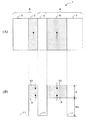
図17は、MTJを用いたMRAMの代表的なセル構成を示す図である。図17(A)に示すように、MRAMは、1つのMTJと1つのMOS(MetalOxide Semiconductor)トランジスタとにより1ビットのメモリセルが構成されている。MOSトランジスタのゲートを読み出し用ワード線に接続し、ソースを接地し、ドレインをMTJの一端に接続し、MTJの他端をビット線に接続している。
【0005】
図17(B)に示すように、MTJは、薄い絶縁膜を2つの強磁性電極で挟み込んだトンネル接合構造を有しており、2つの強磁性電極間の相対的な磁化の向きによってトンネル抵抗が異なるTMR効果を有する。特に、2つの強磁性電極間が平行磁化を持つ場合と、反平行磁化を持つ場合とのTMRの変化率をTMR比と呼び、TMR効果の評価に用いる。
【0006】
MRAMではMTJの磁化状態、すなわち、2つの強磁性電極間の相対的な磁化の向きを、ビット線とこれに直交する書き換え用ワード線(図示せず)のそれぞれに流す電流により誘起される磁場の合成磁場によって平行磁化又は反平行磁化とすることによって情報を記憶する。
【0007】
特定のセル内に記憶された記憶情報を読み出す場合には、セルに接続される特定の読み出し用ワード線に電圧を印加してMOSトランジスタを導通させ、セルに接続される特定のビット線からMTJに読み出し用の電流(以下、「駆動電流」と称する)を流し、TMR効果に基づくMTJの電圧降下を出力電圧として検出することにより記憶された情報を読み出す。
【0008】
【発明が解決しようとする課題】
MTJを用いたMRAMは、強磁性体を用いていることから不揮発、低消費電力、高速といった特徴を有し、さらに、セル構造が簡単であることから高密度集積化に適している。MRAMは次世代不揮発性メモリとして期待されているが、これを実現するためには以下のような解決しなければならない課題がある。
(1)MTJでは平行磁化、反平行磁化の磁化状態に対応して2値の抵抗値を取る。MRAMでは、MTJに駆動電流を流して出力電圧としてこの抵抗値を検出する。従って、高い出力電圧を得るためにはMTJの絶縁膜の厚さを調節しトンネル抵抗を最適化する必要がある。但し、TMR比も絶縁膜の厚さに依存するため、トンネル抵抗の最適化に関して制限が加わる。
(2)さらに、正確に情報の記憶内容を読み出すためには、TMR比を大きく取り、平行磁化と反平行磁化の2つの磁化状態間における出力電圧の比を大きくする必要がある。高いTMR比を実現するためには、スピン分極率の大きな強磁性体を用い、絶縁層の形成方法、材料、膜厚等の最適化が必要である。
(3)MTJを用いたMRAMでは、動作速度を上げるために、MTJに加えるバイアスを大きくする必要がある。しかし、MTJには、強磁性電極間に生じる電圧降下が大きくなるとTMR比が減少するという原理的に避けられない問題がある。すなわち,TMRによる出力電圧の変化率はMTJに生じる電圧降下が大きくなるにしたがって小さくなる。この現象は、TMR効果そのものに基因しており、TMR効果のみによって磁化の状態を読み出す限り避けるのは難しい。
【0009】
以上の課題から、MTJでは高感度に記憶された情報を検出するために、MTJのインピーダンス(接合抵抗)を調節して出力電圧の大きさを最適化する必要がある。さらに、TMR比を大きく取り、平行磁化と反平行磁化の2つの磁化状態間における出力信号の比を大きくする必要がある。また、バイアスによってTMR比が減少しないようにTMR比の耐バイアスが必要となる。
従って、記憶素子の特性に関係なく、出力信号を記憶素子以外の周辺回路によって自由に設計することができれば、上記課題はすべて解決することができる。
【0010】
本発明は、トランジスタ内に含まれる強磁性体に磁化状態によって情報を記憶し、キャリアのスピンの向きに依存するトランジスタの出力特性を用いて情報を読み出す不揮発性メモリを提供することを目的とする。
【0011】
【課題を解決するための手段】
本発明の一観点によれば、スピンフィルタ効果によってスピン偏極ホットキャリアを注入するスピンインジェクタと、この注入された前記スピン偏極ホットキャリアをスピンフィルタ効果によって選別するスピンアナライザと、を有することを特徴とするトランジスタが提供される。従って、スピン偏極ホットキャリアのスピンの向きによりトランジスタの出力特性を制御することができる。
【0012】
前記スピンインジェクタは、第1の強磁性障壁層と、この第1の強磁性障壁層の一端面に接合した第1の非磁性電極層と、上記第1の強磁性障壁層の他端面に接合した第2の非磁性電極層とを有することが好ましい。
【0013】
前記スピンアナライザは、第2の強磁性障壁層と、この第2の強磁性障壁層の一端面に接合した前記第2の非磁性電極層と、上記第2の強磁性障壁層の他端面に接合した第3の非磁性電極層とを有しており、かつ、前記スピンインジェクタと前記第2の非磁性電極層を共通にしていることが好ましい。
【0014】
第1及び第2の強磁性障壁層は、絶縁性の強磁性半導体又は強磁性絶縁体を含んで構成され、これら強磁性障壁層のエネルギーバンド端はスピン分裂によってアップスピンバンドまたはダウンスピンバンドのいずれか一方によって構成されることが好ましい。前記第2の非磁性電極層の厚さは、該第2の非磁性電極層におけるスピン偏極ホットキャリアの平均自由行程以下の厚さであることが好ましい。
【0015】
前記スピンインジェクタは、前記第1の強磁性障壁層のバンド端を構成するスピンバンドと平行なスピンを有するキャリアに対して、トンネル確率が大きく、反平行のスピンを有するキャリアに対してトンネル確率が小さい。従って、前記第1の非磁性電極から前記第1の強磁性障壁層のバンド端を構成するスピンバンドと平行なスピンを有するキャリアを前記第2の非磁性電極層へホットキャリアとして注入することができる。
【0016】
一方、前記スピンアナライザは、前記第2の強磁性障壁層のバンド端におけるスピン分裂によって、前記第2の非磁性電極に注入された前記スピン偏極ホットキャリアのスピンの向きと前記第2の強磁性障壁層のバンド端におけるスピンバンドのスピンの向きとが平行の場合に、前記スピン偏極ホットキャリアを前記第3の非磁性電極層に伝導させるが、前記スピン偏極ホットキャリアと前記第2の強磁性障壁層のバンド端におけるスピンバンドのスピンの向きが反平行の場合には、前記スピン偏極ホットキャリアを前記第3の強磁性電極に伝導させない。
【0017】
従って、同一のバイアス下にあっても前記トランジスタの出力特性は前記第1の強磁性障壁層と前記第2の強磁性障壁層の相対的な磁化の向きに依存し、第1の強磁性障壁層と第2の強磁性障壁層が平行磁化を持つ場合には電流伝送率または電流増幅率が大きく、反平行磁化の場合では電流伝送率または電流増幅率は小さい。
【0018】
また、前記第1の強磁性障壁層に対する前記第2の強磁性障壁層の相対的な磁化の向きによって情報を記憶し、この磁化状態に依存する上記トランジスタの前記出力特性によって情報を読み出す不揮発性記録回路が提供される。この記憶回路では上記トランジスタ単体でメモリセルを構成することができる。
【0019】
本発明の他の観点によれば、強磁性体を含み、キャリアのスピンの向きに依存する出力特性を有するスピントランジスタを用いて、前記強磁性体の磁化方向によって情報を記憶する手段と、前記出力特性から前記スピントランジスタ内に記憶された情報を電気的に読み出す手段とを有することを特徴とする不揮発性記憶回路が提供される。
【0020】
前記スピントランジスタは、磁化の向きを独立に制御できる強磁性体(以下,「フリー層」と称する)、磁化の向きを変化させない強磁性体(以下,「ピン層」と称する)を少なくとも1つずつ有しており、前記フリー層の磁化の向きと前記ピン層の磁化の向きとが同じである第1の状態と、磁化の向きが異なる第2の状態とを記憶情報として保持することが好ましい。
【0021】
前記スピントランジスタは、スピン偏極キャリアを注入する第1の電極構造及び前記スピン偏極キャリアを受け入れる第2の電極構造と、前記第1の電極構造から前記第2の電極構造へ伝導するスピン偏極キャリアの量を制御する第3の電極構造とを備えており、前記ピン層と前記フリー層とは前記第1から第3までの電極構造のいずれかに含まれていることが好ましい。
【0022】
マトリックス状に配置された上記スピントランジスタと、前記第3の電極構造に接続されるワード線と、前記第1の電極構造を接地する第1の配線と、前記第2の電極構造に接続されるビット線とを有する記憶回路が提供される。複数本のワード線が列方向に延在し、これと交差する方向(行方向)に複数本のビット線が延在する。ワード線とビット線との交点の近傍に上記スピントランジスタが配置される。
【0023】
上記記憶回路では、前記スピントランジスタ上で互いに電気的に絶縁された状態で交差する第1の別配線及び第2の別配線とに電流を流すことにより誘起される磁場により、前記フリー層の磁化を反転させ、前記フリー層と前記ピン層との間の相対的な磁化状態を変化させ情報を記憶する(又は書き換える)ことができる。
【0024】
前記第1の別配線および前記第2の別配線、又は、前記第1の別配線又は前記第2の別配線のいずれか一方に代えて、前記ワード線および前記ビット線、又は、前記ワード線又は前記ビット線のいずれか一方を用いることも可能である。
【0025】
上記記憶回路では、前記スピントランジスタ内に含まれる前記フリー層と前記ピン層とが平行磁化を持つ場合における、前記スピントランジスタにおける出力特性に基づき、情報の読み出しを行うことができる。
【0026】
さらに、上記記憶回路において、それぞれのビット線の一端に出力端子が形成され、それぞれのビット線から分岐し負荷を介して電源に接続する第2の配線が設けられた記憶回路が提供される。
【0027】
この場合では、前記フリー層と前記ピン層との相対的な磁化状態に依存する前記スピントランジスタの前記第1と第2の電極構造間に生じる電流による前記負荷の電圧降下に基づいて得られる出力電圧により、情報の読み出しを行うことができる。
上記回路を用いれば、トランジスタ内の磁化状態に応じた出力電圧を負荷と電源により設計できる高集積密度で高速な不揮発性記憶回路が提供できる。
【0028】
【発明の実施の形態】
本発明に係るトランジスタは、特定のスピンの向きを有するスピン偏極ホットキャリアを注入するスピンインジェクタと、この注入されたスピン偏極ホットキャリアを、そのスピンの向きに応じて選別するスピンアナライザとを有している。スピンインジェクタは、Fowler−Nordheimトンネル又はダイレクトトンネル等のトンネル効果が可能な厚さを有する第1の強磁性障壁層と、第1の強磁性障壁層の一端面に接合した第1の非磁性電極層と、第1の強磁性障壁層の他端面に接合した第2の非磁性電極層とを有している。スピンアナライザは、第2の強磁性障壁層と、第2の強磁性障壁層の一端面に接合した第2の非磁性電極層と、第2の強磁性障壁層の他端面に接合した第3の非磁性電極層とを有しており、スピンインジェクタと第2の非磁性電極層とが共通になっている。第2の非磁性電極層の厚さは、この非磁性電極層におけるスピン偏極ホットキャリアの平均自由行程以下の厚さであることが好ましい。
【0029】
すなわち、上記構成を、公知のホットエレクトロントランジスタの構成と比較すると、第1の非磁性電極層と第1の強磁性障壁層とがエミッタ及びエミッタ障壁に対応し、第2の非磁性電極層がベースに対応し、第2の強磁性障壁層と第3の非磁性電極層とがコレクタ障壁とコレクタに対応する。
【0030】
第1及び第2の強磁性障壁層は、絶縁性の強磁性半導体又は強磁性絶縁体を含んで構成される。これらの強磁性障壁層のエネルギーバンドは、磁気的な交換相互作用によりスピン分裂しており、バンド端ではこのスピン分裂によってアップスピンバンドのみ、あるいはダウンスピンバンドのみが存在する。また、一方のスピンバンドのみが存在するエネルギー幅をスピン分裂幅と呼ぶ。
【0031】
スピンインジェクタのスピンフィルタ効果においては、第1の強磁性障壁層に第1の非磁性電極層と第2の非磁性電極層とを介して電圧を印加して生じさせるFowler−Nordheimトンネル又はダイレクトトンネル等のトンネル効果において、第1の非磁性電極層のキャリアのうち第1の強磁性障壁層のバンド端におけるスピンバンドのスピンの向きに一致したスピンの向き(キャリアが電子の場合では、第1の強磁性障壁層の磁化と反平行となるスピンの向きを、キャリアが正孔の場合では、第1の強磁性障壁層の磁化と平行となるスピンの向きを指す。)を有するキャリアのトンネル確率が大きく、一致しないスピンの向き(キャリアが電子の場合では、第1の強磁性障壁層の磁化と平行となるスピンの向きを、キャリアが正孔の場合では、第1の強磁性障壁層の磁化と反平行となるスピンの向きを指す。)を有するキャリアのトンネル確率が小さいことを利用している。
【0032】
スピンアナライザのスピンフィルタ効果は、第2の強磁性障壁層のスピン分裂したバンドにスピンインジェクタからスピン偏極ホットキャリアを注入する場合において、注入されたスピン偏極ホットキャリアのスピンの向きと第2の強磁性障壁層のバンド端におけるスピンバンドのスピンの向きとが平行の場合(第1と第2の強磁性障壁層が平行磁化)に、スピン偏極ホットキャリアは第2の強磁性層のスピンバンド内を伝導して第3の非磁性電極層に到達するが、スピン偏極ホットキャリアと第2の強磁性層のバンド端におけるスピンバンドのスピンの向きが反平行の場合(第1と第2の強磁性障壁層が反平行磁化)には、スピン偏極ホットキャリアは第2の強磁性障壁層を伝導することができないことを利用する。
【0033】
上記トランジスタは以下のように動作する。
第1の非磁性電極層と第2の非磁性電極層との間に第1の電源により第1の電圧を印加し、第2の非磁性電極層と第3の非磁性電極層との間、または、第1の非磁性電極層と第3の非磁性電極層との間に第2の電源により第2の電圧を印加し、第1の強磁性障壁層と第2の強磁性障壁層との相対的な磁化の向きに応じて、第1の非磁性電極層から第2の非磁性電極層に注入されたスピン偏極ホットキャリアを、第2の強磁性障壁層と第2の電源を介して流れる電流に、または、第2の非磁性電極層と第1の電源を介して流れる電流に切り替える。
【0034】
このとき、第1の電圧は、注入されたスピン偏極ホットキャリアのエネルギーが、第2の強磁性障壁層のバンド端におけるスピンバンド端のエネルギーより大きく、スピンバンド端にスピン分裂幅を加えたエネルギーよりも小さくなるように印加する。
【0035】
上記構成によれば、第1の強磁性障壁層のバンド端におけるスピンバンドのスピンの向きと平行なスピンの向きを有する第1の非磁性電極層内のキャリアがFowler−Nordheimトンネルやダイレクトトンネル等のトンネル効果によって第2の非磁性電極層にスピン偏極ホットキャリアとして注入される。第2の非磁性電極層の厚さは、第2の非磁性電極層内におけるスピン偏極ホットキャリアの平均自由行程以下の厚さであるから、注入されたスピン偏極ホットキャリアは、エネルギーを失うことなく、第2の強磁性障壁層に到達する。加えて、スピン偏極ホットキャリアのエネルギーは、第2の強磁性障壁層のバンド端におけるスピンバンド端のエネルギーより大きく、このスピンバンド端にスピン分裂幅を加えたエネルギーよりも小さいエネルギーを有するため、注入されたスピン偏極ホットキャリアのスピンの向きが第2の強磁性障壁層のバンド端におけるスピンバンドのスピンの向きと平行である場合には、スピン偏極ホットキャリアは第2の強磁性障壁層内に発生している電界によって、このスピンバンド内を伝導し、第3の非磁性電極層に輸送され、第3の非磁性電極層と第1の非磁性電極層の間を流れる電流となる。
【0036】
一方、注入されたスピン偏極ホットキャリアのスピンの向きが第2の強磁性障壁層のバンド端におけるスピンバンドのスピンの向きと反平行である場合には、スピン偏極ホットキャリアは第2の非磁性電極層と第2の強磁性障壁層の界面で散乱(または反射)され、第2の非磁性電極層と第1の非磁性電極層との間に流れる電流となる。
【0037】
このように、第1の強磁性障壁層と第2の強磁性障壁層との相対的な磁化の向きが平行か反平行かによって、第1の強磁性障壁層を流れる電流を、第2の強磁性層を介し、第3の非磁性電極層と第1の非磁性電極層の間を流れる電流に、または、第2の非磁性電極層と第1の非磁性電極層との間に流れる電流に切り替えることができる。すなわち、第1の強磁性障壁層と第2の強磁性障壁層の相対的な磁化の向きによって、第2の強磁性障壁層を介して流れる電流を制御することができる。周知のベース接地、または、エミッタ接地のホットエレクトロントランジスタやバイポーラトランジスタの動作と対比させれば、コレクタ電流をベース電流によって制御することに対応するが、本実施の形態によるトランジスタでは、ベース電流によるコレクタ電流の電流増幅率を第1の強磁性障壁層と第2の強磁性障壁層との相対的な磁化の向きによって制御することができる。すなわち、本実施の形態によるトランジスタは、電流増幅率を制御できるトランジスタであり、ベース電流(または第1及び第2の非磁性電極間のバイアス電圧)のみならず、第1の強磁性障壁層と第2の強磁性障壁層の相対的な磁化の向きによってもコレクタ電流を制御することができる。
【0038】
また、第1の強磁性障壁層と第2の強磁性障壁層の保磁力を変えておくか、一方の磁化の向きを固定しておけば、第1の強磁性障壁層と第2の強磁性障壁層のうちのいずれか一方の磁化の向きが反転する適切な強度の磁場を印加することによって、第1の強磁性障壁層と第2の強磁性障壁層との相対的な磁化の向きを平行または反平行のいずれかに任意に変更できる。すなわち、トランジスタ内に情報を記憶させることができる。
【0039】
従って、上記トランジスタを用いてメモリセルを構成することができる。本実施の形態によるトランジスタを用いた不揮発性メモリの一例について以下に説明する。本実施の形態によるトランジスタの第2の非磁性電極層をワード線に接続し、トランジスタの第3の非磁性電極層をビット線に接続し、負荷を介してビット線を電源に接続し、トランジスタの第1の非磁性電極層を接地する。この構成によれば、特定のワード線を選択して第2の非磁性電極層にバイアスを加え、特定のビット線を選択して出力電圧(第1と第2の非磁性電極間に生じる電圧)を検出すれば、出力電圧は、トランジスタの第1の強磁性障壁層と第2の強磁性障壁層の相対的な磁化の向きに応じて変化する。すなわち、相対的な磁化の向きが平行の場合には、出力電圧が小さくなり、相対的な磁化の向きが反平行の場合には出力電圧が大きくなる。従って、記憶された情報を、出力電圧の大小により読み出すことができる。
【0040】
上記不揮発性メモリは、本実施の形態によるトランジスタをエミッタ接地トランジスタとして使用し、コレクタに電源と負荷を付加し、コレクタ電圧を出力電圧とするから、電源電圧と負荷といった周辺回路によって第1と第2の強磁性障壁層が平行磁化である場合の出力電圧と、反平行磁化である場合の出力電圧を所望の値に設計できる。従って、上記不揮発性メモリを用いれば、MTJを用いたMRAMにおける、トンネル抵抗が小さく出力電圧が小さいという問題点並びにTMR比が小さく記憶情報を判別しにくいという問題点、さらに、印加バイアスによって出力電圧の比が小さくなるという問題点を解決することができる。
【0041】
以下、上記トランジスタの構成及び動作について図面に参照しつつ詳細に説明する。尚、以下の説明を分かりやすくするため、本実施の形態によるトランジスタをスピンフィルタトランジスタと称する。
【0042】
図1は、本実施の形態によるスピンフィルタトランジスタの構成を示す図であり、図1(A)は模式的な断面図であり、図1(B)は、図1(A)に示す構成の伝導バンド(又は価電子バンド)のエネルギーバンド図であり、障壁層におけるスピンバンドのスピンの向きを併せて示した図である。但し、キャリアが正孔であればバンド端におけるスピンの向きと磁化の向きは一致するが、キャリアが電子であればバンド端におけるスピンの向きと磁化の向きは逆向きとなる。
【0043】
本実施の形態によるスピンフィルタトランジスタ1は、第1の強磁性障壁層2と、第1の強磁性障壁層2の一端面に接合した第1の非磁性電極層3と、第1の強磁性障壁層2の他端面に接合した第2の非磁性電極層4とを有して構成されるスピンインジェクタ5と、第2の強磁性障壁層6と、第2の強磁性障壁層6の一端面に接合した第2の非磁性電極層4と、第2の強磁性障壁層6の他端面に接合した第3の非磁性電極層7とを有して構成されるスピンアナライザ8と、を有して構成されている。図1(A)から明らかなように、スピンインジェクタ5とスピンアナライザ8とは、第2の非磁性電極層4を共通にしている。
【0044】
第1、第2及び第3の非磁性電極層3、4及び7として、非磁性金属、n型非磁性半導体又はp型の非磁性半導体を用いることができる。また、第2の非磁性電極層4の厚さは、スピンインジェクタから注入されたスピン偏極ホットキャリアの非磁性電極層4内における平均自由行程以下にするのが好ましい。平均自由行程よりもベース幅を短くすることにより、電流伝送率を0.5以上にすることが可能となり、電流増幅作用を得ることができる。
【0045】
第1及び第2の強磁性障壁層2、6としては、絶縁性の強磁性半導体又は強磁性絶縁体を用いることができる。強磁性障壁層のエネルギーバンドは、磁気的な交換相互作用によりスピン分裂しており、バンド端では、アップスピンのみ、あるいはダウンスピンのみが存在するエネルギー領域ができる。このスピン偏極したバンドはスピンバンドと呼ばれ、また、このエネルギー領域幅をスピン分裂幅Δと呼ぶ。
【0046】
図1(B)に示すように、強磁性障壁層2、6に矢印↑を付して示した実線は、アップスピンの存在できるバンドの端部、すなわち、アップスピンバンド端9であり、一方、矢印↓を付して示した実線は、ダウンスピンの存在できるバンドの端部、すなわち、ダウンスピンバンド端10である。図1(B)におけるアップスピンスンド端9とダウンスピンバンド端10との間は、アップスピンのみが存在できる領域である。また、ダウンスピンバンド端10よりも高いエネルギーを有する領域は、アップスピンとダウンスピンとの両方が存在できる領域である。図1(B)は、アップスピンのスピンバンドがダウンスピンのスピンバンドよりも低い場合を例示しているが、これとは逆の状態も可能である。
【0047】
第1の強磁性障壁層2は、第1の非磁性電極層3と第2の非磁性電極層4とに印加する電圧によって、Fowler−Nordheimトンネル(以後、FNトンネルと称する。)又はダイレクトトンネル等のトンネル効果によって第1の非磁性電極層3から第2の非磁性電極層4ヘキャリアの透過が可能な厚さを有している。尚、ダイレクトトンネルとは、キャリアが薄いポテンシャル障壁を直接透過する現象を言う。また,FNトンネルとは、ある印加電圧まではダイレクトトンネルによるトンネル電流が無視でき、ある値以上の電圧を印加することによって生じるポテンシャル障壁上部の三角ポテンシャルをキャリアがトンネルする現象を言う。
【0048】
第1の非磁性電極層3と第2の非磁性電極層4とに印加する電圧は、通常のメモリ回路に使用される電圧範囲で良く、例えば、数百mVから数Vのオーダーである。第2の強磁性障壁層6の厚さは、第2の非磁性電極層4から第3の非磁性電極層7にキャリアの熱放出またはトンネルによる電流(いわゆるリーク電流)が生じない程度に厚くする必要がある。
【0049】
上記の非磁性電極層3、4、7および強磁性電極層2、6は、図1(B)に示すエネルギーバンド構造を形成する。図1(B)中の非磁性電極層部分の実線11は、金属のフェルミエネルギー又はn型(p型)半導体のフェルミエネルギー又は伝導帯の底(価電子帯の頂上)のエネルギーを示す。非磁性電極層部分の実線11に対する強磁性障壁層2、6の低い方のエネルギー障壁をφCで示し、スピン分裂幅をΔで表す。強磁性障壁層2と6は、異なる値のφCとΔを有しても良いが、以下では、強磁性障壁層2と6とで同じ値のφCとΔを持つ場合について示す。
【0050】
キャリアが電子である場合は、非磁性電極層3、4、7に非磁性金属又はn型半導体を用い、強磁性障壁層2、6に絶縁性の強磁性半導体又は強磁性絶縁体を用いる。この場合、強磁性障壁層2、6のアップスピンバンド端9及びダウンスピンバンド端10は、伝導帯の底がスピン分裂したものである。また、キャリアを正孔とする場合には、非磁性電極層3、4、7としてp型半導体を用い、強磁性障壁層2、6に絶縁性の強磁性半導体又は強磁性絶縁体を用いる。この場合には、強磁性障壁層2、6のアップスピンバンド端9及びダウンスピンバンド端10は、価電子帯頂上がスピン分裂したものである。
【0051】
次に、上記スピンフィルタトランジスタの動作原理について詳しく説明する。以後の説明においては、説明を簡単にするために、ホットエレクトロントランジスタの表記法を併用して説明する。すなわち、第1の非磁性電極層3と第1の強磁性障壁層2をエミッタ21、第2の非磁性電極層4をベース22、第2の強磁性障壁層6と第3の非磁性電極層7をコレクタ23と称し、第1の非磁性電極層3をエミッタ電極3、第3の非磁性電極層7をコレクタ電極7と称する。また、キャリアが電子の場合を例にして説明する(キャリアがホールの場合も、動作原理は本質的に同等であるので説明を省略する)。
【0052】
図2は、本実施の形態によるトランジスタのエミッタ、ベース、コレクタ間にベース接地バイアス電圧を加えた場合のエネルギーバンド図であり、図2(A)は第1及び第2の強磁性障壁層の磁化の向きが互いに平行な場合、図2(B)は第1及び第2の強磁性障壁層の磁化の向きが互いに反平行な場合であり図2(A)に対応する図である。エミッタ21とベース22間にバイアス電圧VEBを、ベース22とコレクタ23との間にバイアス電圧VCBを加えている。このときVEBの大きさは(Φc<qVEB<Φc+Δ)の関係を満たすように設定する。但し、qは電荷素量である。
【0053】
エミッタ21は、ベース22にスピン偏極したホットエレクトロンを注入するスピンインジェクタとして働く。すなわち、バイアス電圧VEBによってキャリアをエミッタ電極3から第1の強磁性障壁層2をトンネルにより通過させる場合に、第1の強磁性障壁層2の伝導帯がスピン分裂しているため、エミッタ電極3に存在するアップスピン電子24とダウンスピン電子25とでは感じる障壁高さが異なる。
【0054】
すなわち、図2(A)では、アップスピン電子24が感じる障壁高さは、第1の強磁性障壁層2のアップスピンバンド端9までのエネルギー、すなわちΦcであり、ダウンスピン電子25が感じる障壁高さは、第1の強磁性障壁層2のダウンスピンバンド端10までのエネルギー、すなわち、Φc+Δである。従って、ベース−エミッタ電圧を制御することにより、感じる障壁高さが低い方のスピンを持つ電子、この場合にはアップスピンを持つ電子24を選択的にベース22にトンネル注入させることができる(この現象をスピンフィルタ効果と称する。)。
【0055】
一方、上記トランジスタのコレクタ23は、ベース22に注入されたスピン偏極ホットエレクトロンの向きを選別するスピンアナライザとして働く。すなわち、バイアス電圧VEBによってホットな状態となりベース22に注入されたスピン偏極ホットエレクトロン26は、ベース22の幅をスピン偏極ホットエレクトロン26の平均自由行程以下に設定しているため、ベース22とコレクタ23との界面までエネルギーを失うことなく、すなわち、バリスティックに到達することができる。コレクタ23の第2の強磁性障壁層6も、伝導帯のスピン分裂によって障壁高さの異なる2つの障壁が生じている。図2(A)に示すように、第1及び第2の強磁性障壁層2、6の磁化の向きが互いに平行な場合、スピン偏極ホットエレクトロン26と平行なスピンを持つ第2の強磁性障壁層6のアップスピンバンド端9は、スピン偏極ホットエレクトロン26のエネルギーより低いため、スピン偏極ホットエレクトロン26は、第2の強磁性障壁層6を越えてコレクタ電極7へ伝導し、コレクタ電流ICとなる。
【0056】
一方、図2(B)に示すように、第1及び第2の強磁性障壁層2、6の磁化方向を互いに反平行にした場合、ベース22には、ダウンスピンを有するスピン偏極ホットエレクトロン27が注入されるが、ダウンスピンを有する第2の強磁性障壁層6のダウンスピンバンド端10がスピン偏極ホットエレクトロン27のエネルギーよりも高いので、スピン偏極ホットエレクトロン27は第2の強磁性障壁層6の伝導帯を伝導できず、ベース22とコレクタ23との界面においてスピン依存散乱(又は反射)を受けてエネルギーを失い、ベース電流IBとなる。
【0057】
このように、エミッタ22の第1の強磁性障壁層2とコレクタ23の第2の強磁性障壁層6との相対的な磁化の向きにより、エミッタからコレクタヘ流れる電流の電流伝送率は大きく異なる。換言すれば、ベース電流によるコレクタ電流の電流増幅率が大きく異なる。
【0058】
図3は、本実施の形態によるスピンフィルタトランジスタのベース接地における静特性を示す図である。横軸は、図面上右方向にコレクタ−ベース電圧VCB、左方向にエミッタ−ベース電圧VEBを示し、縦軸は、エミッタ電流IE、ベース電流IB、コレクタ電流ICを示している。図3(A)は、エミッタとコレクタの強磁性障壁層の磁化方向が平行の場合の静特性を、図3(B)は、反平行の場合の静特性を示している。尚、図3(A)、図3(B)において、αは電流伝送率、βは電流増幅率を示し、また、添え字、↑↑及び↓↑はそれぞれ、エミッタとコレクタの強磁性障壁層の相対的な磁化方向が平行の場合と、反平行の場合とを示す。
【0059】
図3(A)に示すように、エミッタとコレクタの磁化方向が平行の場合には、エミッタ電流IEのほとんどがコレクタ電流ICとすることができる。図3(B)に示すように、磁化方向が反平行の場合には、エミッタ電流IEのほとんどがベース電流IBとすることができる。公知のホットエレクトロントランジスタ又はバイポーラトランジスタと同様に、本実施の形態によるトランジスタにおいても、ベース電流IBによりコレクタ電流ICを制御することができる。加えて、第1と第2の強磁性障壁層の相対的な磁化の向きによっても、電流増幅率を制御することができる。
【0060】
本実施の形態によるスピンフィルタトランジスタの強磁性障壁層としては、EuS、EuSe、EuO等の強磁性半導体を使用することができる。また、R3Fe5O12(Rは希土類元素を示す)等の強磁性絶縁体も使用することができる。非磁性電極層としては、非磁性体であれば良く、例えば、AlやAuなどの金属や、高濃度に不純物ドープされたSiやGaAS等の非磁性半導体でも良い。例えば、強磁性障壁層として、EuS、非磁性電極層としてAlを用いた場合、障壁高さΦC=1.4eVであり、スピン分裂幅Δ=0.36eVである。また、本実施の形態によるスピンフィルタトランジスタは、上記の材料を用い、公知の分子線エピタキシャル成長法、真空蒸着法、スパッタリング法等によって製造することができる。
【0061】
次に、本発明のスピンフィルタトランジスタをメモリセルとして用いた不揮発性メモリについて説明する。
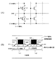
図4(A)は、本実施の形態によるスピンフィルタトランジスタ1を用いたメモリセルの一構成例を示す図である。図4(A)に示すメモリセルでは、スピンフィルタトランジスタを多数マトリクス状に配置し、エミッタ端子Eを接地してコレクタ端子Cとベース端子Bとをそれぞれ読み出し用ビット線BLと読み出し用ワード線WLとに接続している。また、書き換え用ワード線と書き換え用ビット線を、上記スピンフィルタトランジスタ上で他の配線と電気的に絶縁した状態で交差するように配置する。この書き換え用ワード線と書き換え用ビット線として、上記の読み出し用ビット線BLと読み出し用ワード線WLとを併用しても良い。図4(A)は、併用した場合のセル構成を示す図である。図4(A)の場合では、スピンフィルタトランジスタ単体でメモリセルを構成できるとともに、配線に関しても非常に単純な構成にすることができる。従って、微細化に適したレイアウトを容易に構成することができる。図4(B)も同様のセル構成を用いている。
【0062】
次に、本実施の形態によるメモリ回路について図4(B)を参照して説明する。本実施の形態によるメモリ回路41は、スピンフィルタトランジスタ1(図1)のベースである第2の非磁性電極4をワード線42に接続し、スピンフィルタトランジスタ1のコレクタ電極である第3の非磁性電極7をビット線43に接続し、ビット線43を、負荷(RL)44を介して電源(VCC)45に接続し、スピンフィルタトランジスタ1のエミッタ電極である第1の非磁性電極3を接地した構成を有している。ここでは負荷として純抵抗を用いているが、トランジスタによる能動負荷を用いても良い。
【0063】
特定のメモリセルの記憶情報を読み出すには、特定のワード線42を選択してエミッタ−ベース間にバイアスを加え、ビット線43に負荷抵抗44を介して電源45の電源電圧VCCを印加し、ビット線43にあらわれる出力電圧VOの大小によって記憶情報を読み出す。図4(C)の縦軸はコレクタ電流IC、横軸はコレクタ−エミッタ間電圧VCEを表し、スピンフィルタトランジスタのIC―VCE特性と、負荷抵抗44による負荷直線46を同一の図の上に示したものである。出力電圧VOは、これらの特性の交点から決定される。すなわち、第1及び第2の強磁性障壁層2、6の相互の磁化方向が、平行の場合と反平行の場合との出力信号は、それぞれ、図4(C)に示すように、VO↑↑とVO↓↑になる。VO↑↑及びVO↓↑の絶対値、及び、VO↑↑とVO↓↑の比は回路パラメータ(RL及びVCC)により最適化できる。このように、本実施の形態による不揮発性メモリデバイスは、MTJのように素子自身の構造を調節することなく、必要な大きさの出力信号及び出力信号の比を得ることができる。
【0064】
本実施の形態によるトランジスタにおいて利用するスピンフィルタ効果は、強磁性体におけるバンドのスピン分裂を利用した効果であり、MTJのTMR効果に比べてスピンの選択率が高い。べース幅をスピン偏極ホットキャリアの平均自由行程以下に設定すれば、第1及び第2の強磁性障壁層間の相対的な磁化状態が、平行磁化の場合では、電流伝送率α(=IC/IEで定義)は0.5以上になりうるが、反平行磁化の場合では、電流伝送率は極めて小さい。すなわち、平行磁化の場合と反平行磁化の場合との電流伝送率の変化は、電流増幅率β(=IE/IBで定義される)でみると、さらに増幅されていることになる。この磁化状態で大きく異なるスピンフィルタトランジスタの出力特性に対して、上述した周辺回路により出力信号の最適化を行うことにより、容易に所望の出力信号の絶対値及び所望の出力信号の比を得ることができる。
【0065】
次にキャリアのスピンの向きに依存する出力特性を有するトランジスタ(以下,「スピントランジスタ」と称する)を用いた不揮発性記憶回路について説明する。
本発明に係る記憶回路は、スピントランジスタを用いた不揮発性記憶回路に関するものである。スピントランジスタは強磁性金属や強磁性半導体などの強磁性体をトランジスタ内に含み、この磁化状態によってキャリアのスピンの向きを制御して出力特性を変化させる。スピントランジスタ内部における強磁性体の磁化状態に基づき情報を記憶し、スピントランジスタ内部の磁化状態を反映したトランジスタの出力特性を用いて情報の読み出しを行う。スピントランジスタを用いれば1つのスピントランジスタで1ビットの不揮発性メモリセルを構成することが可能であり、また、記憶情報に対する出力信号の値を、このメモリセルに接続した周辺回路によって最適化することが可能である。
【0066】
より詳細には、スピントランジスタは、磁化の向きを磁場等によって独立に制御できる強磁性体層(フリー層)と、磁化の向きが固定されている強磁性体層(ピン層)と、を少なくとも1つずつ有しており、同一バイアス下であっても、フリー層とピン層との相対的な磁化の向きによってトランジスタの出力特性を制御できるトランジスタである。フリー層の磁化の向きを磁場等により変化させることにより、フリー層とピン層との相対的な磁化状態を平行磁化又は反平行磁化の2つの状態を実現することができる。この2つの磁化状態が2値の記憶情報に対応する。
【0067】
スピントランジスタでは、スピン依存散乱、トンネル磁気抵抗効果、スピンフィルタ効果等のキャリアのスピンの向きに依存して変化する伝導現象に基づいて、トランジスタ内の磁化状態に応じた出力特性を得ることが出来る。スピントランジスタは、スピン偏極キャリアを注入する第1の電極構造及びスピン偏極キャリアを受け入れる第2の電極構造と、第1の電極構造から第2の電極構造へ伝導するスピン偏極キャリアの量を制御する第3の電極構造とを備えている。
【0068】
スピントランジスタでは、スピンに依存する伝導現象以外は、一般的なトランジスタと同様の動作原理に基づき動作する。従って、スピントランジスタはバイポーラトランジスタ等の電流駆動型トランジスタと電界効果トランジスタ等の電圧駆動型トランジスタとに分類することができる。電流駆動型トランジスタでは、第1の電極構造はエミッタに、第2の電極構造はコレクタに、第3の電極構造はベースにそれぞれ対応する。本実施の形態で説明したスピンフィルタトランジスタはこの電流駆動型に分類される。
【0069】
また、電圧駆動型トランジスタの場合には、第1の電極構造はソースに、第2の電極構造はドレインに、第3の電極構造はゲートにそれぞれ対応する。スピントランジスタにおけるコレクタ電流またはドレイン電流は、同一バイアス下にあっても、スピントランジスタ内に含まれる強磁性体の磁化状態で変化する。
【0070】
スピントランジスタの詳細については後述し、以下、スピントランジスタの一般的な出力特性と、スピントランジスタを用いた不揮発性メモリについて説明する。以下では、スピントランジスタ内にフリー層とピン層の強磁性体を含み、フリー層に磁場を印加することによって、フリー層とピン層の相対的な磁化状態を平行磁化または反平行磁化を実現することができるとする。また、この磁化状態はフリー層の保磁力以上の磁場が印加されない限り安定に存在できるものとする。
【0071】
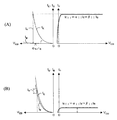
図5(A)に、電流駆動型スピントランジスタの出力特性の例を模式的に示す。通常の電流駆動型トランジスタと同様に、コレクタ電流ICはベース電流IBの大きさによって制御できるが、コレクタ電流の大きさはスピントランジスタ内に含まれる強磁性体の磁化状態にも依存する。図5(A)の場合では,スピントランジスタに同じバイアスを加えていても(IB=IB1)、平行磁化の場合ではコレクタ電流IC↑↑は大きく、反平行磁化の場合ではコレクタ電流IC↓↑は小さい。
【0072】
図5(B)に、電圧駆動型スピントランジスタの出力特性の例を模式的に示す。通常のMOSトランジスタなどの電界効果トランジスタと同様に、ゲートーソース電圧(VGS)がしきい値VTよりも小さい場合(VGS<VT)には、スピントランジスタは遮断状態でドレイン電流はほとんど生じない。VT以上のVGSを印加すれば、スピントランジスタは導通状態となるが、同じバイアス下(VGS=VGS1)においても、スピントランジスタ内に含まれる強磁性体が平行磁化を持つ場合と反平行磁化を持つ場合とでドレイン電流値は異なる。図3(B)の場合では,平行磁化を持つ場合には、ドレイン電流ID↑↑は大きく、反平行磁化を持つ場合には、ドレイン電流ID↓↑は小さい。
【0073】
従って、スピントランジスタでは、電流駆動型,電圧駆動型ともにデバイス内に含まれるフリー層とピン層の相対的な磁化の向きを、コレクタ電流またはドレイン電流の大きさに基づいて、電気的に検出することができる。また、上記のように強磁性体では、外部からフリー層の保磁力以上の磁場が印加されない限り磁化の向きを安定に保持することができる。このため、スピントランジスタでは、デバイス内に含まれるフリー層とピン層の相対的な磁化状態を平行磁化または反平行磁化にすることによって2値の情報を記憶することができる。従って、スピントランジスタを用いれば、1つのスピントランジスタのみで1ビットの不揮発性メモリセルを構成することができる。
【0074】
以下、電圧駆動型のスピントランジスタを用いた場合を例にして、スピントランジスタを用いた不揮発性メモリについて詳述する。電流駆動型のスピントランジスタをメモリセルに用いた場合も同様にして構成することができる。
【0075】
図6(A)は、スピントランジスタを用いたメモリセルの構成例を示す図である。図6(B)は、このメモリセルに基づいて形成した記憶回路の構成例を示す図である。図6(A)と図6(B)との関係は、図4(A)と図4(B)との関係と同様である。図6(A)に示すメモリ回路では、スピントランジスタ150を多数マトリクス状に配置し、ソースSを接地してドレインDとゲートGとをそれぞれ読み出し用ビット線BLと読み出し用ワード線WLとに接続している。また、書き換え用ワード線と書き換え用ビット線を、上記スピントランジスタ150上で他の配線と電気的に絶縁した状態で交差するように配置する。この書き換え用ワード線と書き換え用ビット線として、上記の読み出し用ビット線BLと読み出し用ワード線WLとを併用しても良い。図6(A)、(B)は、併用した場合の構成を示す図である。図6(A)、(B)の場合では、1つのスピントランジスタのみでメモリセルを構成できるとともに、配線に関しても非常に単純な構成に配置することができる。
特に、MOSトランジスタに類似の形態を有する電圧駆動型のスピントランジスタでは、隣り合うメモリセルでソースを共通にするなど、微細化に適したレイアウトを容易に構成することができる。
以下、上述した書き換え/読み出し用ビット線および書き換え/読み出し用ワード線を、単に、それぞれビット線BL、ワード線WLと呼ぶ。
【0076】
情報の書き換えは、選択したメモリセル上で交差するビット線BLとワード線WLとに電流を流し、それぞれの配線に流れる電流によって誘起される磁界の合成磁界によって選択されたメモリセルのフリー層を反転させて情報を書き換える。この際、選択セルと同一のビット線BL又はワード線WLに接続している非選択セルが磁化反転しないようにするため、一方の配線のみからの磁界では磁化反転を生じないようにそれぞれの配線に流す電流値を設定しておく。
【0077】
情報の読み出しは、選択セルに接続されたワード線WLに電圧を印加してスピントランジスタを導通させてから、ビット線BLに電圧を印加してドレイン電流の大きさを検出する。このドレイン電流の大きさに基づき、フリー層とピン層との相対的な磁化状態を検出することができる。
【0078】
図6(B)は、図6(A)に示すメモリ回路のビット線端に出力端子VOと、この出力端子VOから分岐して負荷を介し電源電圧VDDに接続したメモリ回路である。図6(C)に、図6(B)に示したメモリセルの静特性と動作点とを示す。ここでは、負荷としてデプレッション型MOSトランジスタによる能動負荷160を用いているが、図4(B)のように純抵抗を用いても良い。図6(C)に示すように、情報の読出し時にはスピントランジスタ150のゲートにゲート電圧VGSを印加し、ビット線BLに負荷を介して電源電圧VDDを印加すれば、能動負荷による動作点は、ピン層とフリー層と間の磁化状態に応じて図6(C)中の負荷曲線上を動き(図中のP11とP12)、平行磁化と反平行磁化との場合の出力信号V0はそれぞれ図中のV0↑↑とV0↑↓となる。それぞれの出力信号の絶対値および比(V0↑↑/V0↑↓)は,能動負荷のトランジスタ特性やVDDなどの周辺回路のパラメータにより最適化することができる。例えば、スピントランジスタの静特性と能動負荷による負荷曲線との交点を最適化することにより、ドレイン電流比ID↑↑/ID↑↓が小さい場合でも大きな出力信号比を得ることができる。また、D↑↑とID↓↑の値がメモリセルによってばらついていても、能動負荷の飽和電流がID↓↑より大きく、IC↑↑より小さければ、出力電圧はほとんど変動しないようにできる。さらに、情報の読み出しにセンスアンプを用いないため、高速の読み出しが可能となる。したがって、本実施の形態による記憶回路では、所望の大きさの出力信号を容易に得ることができて、さらに高速読み出しが可能になるという利点を有する。
【0079】
従来のMTJとMOSトランジスタとを用いたメモリセルでは、MTJの抵抗による出力電圧をセンスアンプによって読み取るが、出力電圧はMTJに流す電流値とMTJのインピーダンス(接合抵抗)によって決定され、出力電圧比を周辺回路で自由に調節することはできない。
【0080】
以下に、本実施の形態による不揮発性メモリ回路に適用可能なスピントランジスタの構造について図面を参照して説明する。以下、FMは強磁性金属、FSは電気伝導性強磁性半導体、IFSは絶縁性強磁性半導体、NMは非磁性体の略号である。特に、NM金属は非磁性金属、NM半導体は非磁性半導体を表す。まず、電流駆動型のスピントランジスタ群について説明を行う。
【0081】
図7は、ホットエレクトロントランジスタ型のスピントランジスタのエネルギーバンド図である。スピントランジスタ200は、エミッタ201とベース205とが、FMまたはFSで構成されている。より詳細には、スピントランジスタ200は、FM(又はFS)からなるエミッタ201と、NMからなるエミッタ障壁203と、FM(又はFS)からなるベース205と、NMからなるコレクタ障壁207と、NMからなるコレクタ211と、を有している。NMとしては非磁性金属または非磁性半導体を用いることができる。
【0082】
図7に示すスピントランジスタ200では、エミッタ201からエミッタ障壁203を介してスピン偏極ホットキャリアをベース205にトンネル注入する。エミッタ201とベース205とが平行磁化の場合には、注入されたスピン偏極ホットキャリアは、ベース205内でほとんどスピン依存散乱を受けないため、バリスティックにベース205を通過できるようにベース幅を設定しておけば,コレクタ障壁207を越えてコレクタ211に到達する。すなわち、通常のホットエレクトロントランジスタと同様のトランジスタ動作をする。
【0083】
一方、エミッタ201とベース205とが反平行磁化を持つ場合には、エミッタ201からベース205に注入されたスピン偏極ホットキャリアは、ベース205内でスピン依存散乱によりエネルギーを失い、コレクタ障壁207を越えることができずにベース電流となる。すなわち、エミッタ201とベース205とが反平行磁化の場合には、両者が平行磁化の場合に比べて電流伝送率が低下する。従って、スピントランジスタ200に同じバイアスが印加されていても、エミッタ201とベース205との相対的な磁化状態の違いにより、電流伝送率又は電流増幅率が異なる。また、スピントランジスタ200はコレクタ障壁の障壁高さを適切に選択するなどにより室温動作も可能である。
【0084】
スピントランジスタ200は、エミッタ−ベース間が平行磁化を持つ場合と反平行磁化を持つ場合とのそれぞれにおける電流伝送率の比を大きくするためにはスピン依存散乱が有効に作用できるようにベース幅を長くとる必要がある。一方、ベース幅を長くすると、エミッタとベースとが平行磁化の場合においても、電流伝送率が小さくなり、例えば0.5を下回り、増幅作用が失われるといったトレードオフが存在する。
【0085】
図8は、ベースへのスピン注入機構として熱放出を利用したホットエレクトロントランジスタ型のスピントランジスタのエネルギーバンド図である。図8に示すように、スピントランジスタ220は、FM(又はFS)からなるエミッタ221と、FM(又はFS)からなるベース225と、両者の間に設けられたNMからなるエミッタ障壁223と、を有している。さらに、ベース225とエミッタ障壁223との接合の反対側に、NMからなるコレクタ障壁227と、NMからなるコレクタ231と、を有している。エミッタ障壁223およびコレクタ障壁227には非磁性半導体を用いることができる。またコレクタ231は非磁性半導体または非磁性金属を用いることができる。
【0086】
エミッタ221とエミッタ障壁223との間はオーミックコンタクトまたはトンネルコンタクトを形成する。ベース225とエミッタ障壁223との間、ベース225とコレクタ障壁227との間は、図9に示すバンド不連続を有するように接合を形成する。このバンド不連続は、NM半導体/FM間のショットキー接合やNM半導体/FS間のへテロ接合により実現することができる。或いは、FSとFMとでショットキー接合を形成し、この際に生じるショットキー障壁をエミッタ障壁とし、FSをエミッタとし、FMをベースとして構成しても良い。
【0087】
エミッタ221に対してベース225にバイアスを印加することによりエミッタ221からエミッタ障壁223に拡散したスピン偏極キャリアは、熱放出によりベース225へホットキャリアとして注入される。エミッタ221とベース225とが平行磁化を持つ場合には、ベース225に注入されたスピン偏極ホットキャリアはスピン依存散乱を受けることなくコレクタに到達することができるが、エミッタ221とベース225とが反平行磁化の場合では、スピン偏極ホットキャリアはスピン依存散乱によってベース電流となる。このトランジスタ220においても、ベースにおけるスピン依存散乱を用いているために上記スピントランジスタ200と同様に、平行磁化および反平行磁化を持つ場合のそれぞれにおける電流伝送率の比と、平行磁化の場合における電流伝送率との間にトレードオフの関係が存在する。但し、トンネル注入を用いた上記スピントランジスタ200に比べて、電流駆動力を大きく取れるといった特徴や、室温動作を実現しやすいといった特徴がある。
【0088】
図9は、スピンフィルタ効果を用いたホットエレクトロントランジスタ型のスピントランジスタのエネルギーバンド図である。このトランジスタについては既に詳細に説明したが、簡単にその特徴を説明する。図9に示すスピントランジスタ240は、エミッタ障壁243およびコレクタ障壁247がIFSにより構成されている。NM金属(またはNM半導体)からなるエミッタ241からは、エミッタ障壁243のスピンフィルタ効果により選択的に一方のスピンを持つキャリアのみをNM金属(又はNM半導体)からなるベース245に注入することができる。ベース幅をスピン偏極率ホットキャリアの平均自由行程以下に設定してあれば、ベース245に注入されたスピン偏極率ホットキャリアは、バリスティックにベース245を伝導する。このとき、コレクタ障壁247のアップスピンバンド(図9では上向き矢印が付されているスピンバンド端)とダウンスピンバンド(図9では下向き矢印が付されているスピンバンド端)とのエネルギー分裂幅内にスピン偏極ホットキャリアが注入されるようにスピントランジスタ240をバイアスしておく。エミッタ障壁243とコレクタ障壁247とが平行磁化を持つ場合には、ベース245に注入されたスピン偏極ホットキャリアは、コレクタ障壁247のスピンフィルタ効果によって、コレクタ障壁247における低いエネルギーのスピンバンドによる障壁を乗り越え、NM金属(またはNM半導体)からなるコレクタ251へ伝播することができる。一方、エミッタ障壁243とコレクタ障壁247とが反平行磁化を持つ場合では、コレクタ障壁247のスピンフィルタ効果によって、スピン偏極ホットキャリアのほとんどはコレクタ障壁247を乗り越えることができずにベース電流となる。
【0089】
従って、スピントランジスタ240において、エミッタ障壁243とコレクタ障壁247との相対的な磁化の向きによって、電流伝送率(又は電流増幅率)が異なる。スピンフィルタ効果はスピンの選択率が極めて大きいため、このトランジスタでは平行磁化と反平行磁化のそれぞれの場合における電流伝送率の比を大きくすることができる。
【0090】
また、スピントランジスタ240では、ベース幅を十分に短くすることが可能である。従って、図7、図8に示すスピン依存散乱を利用したスピントランジスタと異なり、ベース幅に関連する電流増幅率とスピン選択性との間のトレードオフは存在しないという利点がある。
【0091】
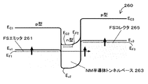
図10は、トンネルベーストランジスタ型のスピントランジスタのエネルギーバンド図である。図10に示すように、トンネルベーストランジスタ型のスピントランジスタ260では、エミッタ261とコレクタ265にp型(又はn型)のFSを用い、トンネルベース263にn型(又はp型)のNM半導体を用いている。エミッタ−ベース間及びベース−コレクタ間は、正孔(又は電子)に対してベース263が障壁になるようなタイプIIのヘテロ接合を用いることが好ましい。また、ベース幅はエミッタからコレクタにトンネル電流が生じる程度に薄くする。
【0092】
図10に示す構造において、エミッタ261とコレクタ265とが平行磁化を持つ場合では、エミッタの多数スピンを有するキャリアは、容易にコレクタ265にトンネルできるためトンネルコンダクタンスは大きいが、エミッタ261とコレクタ265とが反平行磁化を持つ場合では、トンネル磁気抵抗効果(TMR効果)によってトンネルコンダクタンスは小さい。従って、エミッタ261とコレクタ265との相対的な磁化の状態によってコレクタ電流の大きさを制御することができる。
【0093】
このスピントランジスタ260におけるTMR比を大きくとることができれば、エミッタ−コレクタ間の磁化状態に依存するコレクタ電流の変化を大きくすることが可能となる。スピントランジスタ260で、TMR効果を有効に発揮させるためには、ベース−コレクタ接合に逆バイアスを印加した場合に空乏層がコレクタ側に広がらないようにすることが好ましい。但し、空乏層がベース側に広がると、コレクタ電流の飽和特性に問題が生じる可能性は存在する。
【0094】
上記トランジスタ260において、ベース層に空乏層が広がらないようにベース層を高濃度ドープし、ベース−コレクタ接合の空乏層がコレクタ側に広がるようにした場合には、ベースにおけるTMR効果は期待できないがコレクタに注入されたキャリアはコレクタ内でスピン依存散乱による抵抗を生じる。このスピン依存散乱を用いればエミッタ−コレクタ間の磁化状態によりコレクタ電流の大きさを変えることができる。但し、スピン依存散乱による抵抗変化は小さいことからTMR効果を用いる場合に比べてその効果が大きくない可能性がある。
【0095】
次に、電圧駆動型スピントランジスタ群について図面を参照して説明する。
図11は、MOSトランジスタ型のスピントランジスタの断面構造を示す図である。図11に示すように、MOSトランジスタ型のスピントランジスタ300は、NM半導体301上に、FMからなるソース303と、FMからなるドレイン305と、ゲート絶縁膜307を介してゲート電極311と、が形成された構造を有している。FMとNM半導体とのショットキー接合をソース303とドレイン305に用いており、その他の構成は通常のMOSトランジスタと同様である。
【0096】
ソース303からNM半導体301におけるゲート絶縁膜307の直下に形成されるチャネルに注入されたスピン偏極キャリアは、このチャネルを通ってドレイン305に到達する(以下、簡単のためチャネルに注入されたスピンのゲート電界によるRashba効果の影響を無視する)。ソース303とドレイン305とが平行磁化を持つ場合は、ドレイン305に注入されたスピン偏極キャリアはスピン依存散乱を受けることはないが、反平行磁化を持つ場合ではドレイン電極305においてスピン依存散乱による抵抗を生じる。
【0097】
従って、このトランジスタ300では、ソース−ドレイン間の相対的な磁化の向きによってコンダクタンスが異なる。
また、ソース303とドレイン305にFSを用いることにより半導体301との間にpn接合を形成し、ソースおよびドレインを形成することも可能である。
【0098】
図12は、変調ドープトランジスタ型のスピントランジスタの断面構造を示す図である。このスピントランジスタ320は、第1のNM半導体321と第2のNM半導体327との界面に生じる2次元キャリアガスに対するFM(又はFS)からなるソース323と、FM(又はFS)からなるドレイン325と、ゲート電極331とから形成された構造を有している。ソース323とドレイン325が強磁性体で構成されている以外は、通常の通常の変調ドープトランジスタと同様である。
【0099】
ソース323から、スピン偏極キャリアを、二次元キャリアガスにより形成されたチャネル333に注入する。ドレイン325に達したスピン偏極キャリアは、ドレイン325でのスピン依存散乱のため、ソース323とこのドレイン325との相対的な磁化の向きによって相互コンダクタンスが異なる。
【0100】
図13は、チャネル領域にFSを用いたMOSトランジスタ型のスピントランジスタの断面図である。図13に示すスピントランジスタ340は、FS341上に、FMからなるソース343と、NM(又はFM,FS)からなるドレイン345と、ゲート絶縁膜347を介してゲート電極351と、が形成された構造を有している。FMとFSとのショットキー接合をソース343に用いており、その他の構成は通常のMOSトランジスタと同様である。
【0101】
ソース343からショットキー障壁を通してスピン偏極キャリアをチャネル341中にトンネル注入する。このトンネル注入時のTMR効果及びFS341のチャネル内におけるスピン依存散乱によって、ソース343とFS341の相対的な磁化の向きに依存する相互コンダクタンスを実現する。
【0102】
図14に断面構造を示すスピントランジスタ360は、絶縁性のNMトンネル障壁365をFM(又はFS)からなるソース361とFM(又はFS)からなるドレイン363とで挟み込んだトンネル接合構造を有しており、トンネル障壁365に対して電界を印加できるようにゲート電極371を配置したスピントランジスタである。
【0103】
トンネル障壁365の膜厚は、ソース−ドレイン間のバイアスのみを印加した場合にFowler−Nordheim(FN)トンネルが生じない程度の厚さに設定しておくことが好ましい。ソース−ドレイン間にバイアスを印加することによって生じるトンネル障壁バンド端の三角ポテンシャルをゲート電圧により変化させることによって、FNトンネルを誘起しドレイン電流を得る。
【0104】
ソース361から注入されたスピン偏極キャリアは、ソース361とドレイン363の相対的な磁化状態に応じて、ドレイン363でスピン依存散乱を受ける。従って、ソース−ドレイン間の相対的な磁化の向きによってトランジスタの相互コンダクタンスを制御できる。
【0105】
図15に断面構造を示すスピントランジスタ380は、図14に示すスピントランジスタ360のトンネル障壁をIFSからなるトンネル障壁385に置き換えたものである。ソース381はFM又はFSである必要があるが、ドレイン383は強磁性体でなくてもよい。IFSトンネル障壁層385では、キャリアのスピンの向きによって障壁高さが異なるが、ソース381とトンネル障壁385とが平行磁化を持つ場合にトランジスタが導通状態となるようにソース−ドレイン間およびソース−ゲート間にバイアスを加える。これと同じバイアス条件下において、ソース381とトンネル障壁385が反平行磁化を持つ場合には、ソース381の多数スピンから見たトンネル障壁の高さが高くなるため、スピン偏極キャリアのトンネル確率が減少してドレイン電流が低減する。このスピンフィルタ効果によるスピン選択率は極めて大きいため、スピン分極率の大きな強磁性体をソース381として用いれば、ソース−ドレイン間の相対的な磁化の向きによる相互コンダクタンスの変化を大きくすることができる。
【0106】
以上、説明した種々のスピントランジスタは、いずれも図4又は図6に示す記憶回路用のメモリセルとして用いることができる。
また、2つの図11、14、15に示した電圧駆動型のスピントランジスタのソースを1つのソースで共通とした構造を形成することも可能である。図16(A)は共通ソース構成を有するメモリセルの構成例を示す図である。図16(B)は、共通ソース構成を有するメモリセルの断面構造例を示す図である。
【0107】
図16(A),(B)に示すメモリセル構造は、互いに隣接する第1のスピントランジスタTr1と第2のスピントランジスタTr2と、第1のスピントランジスタTr1のゲート電極G1と第2のスピントランジスタTr2のゲート電極G2とを共通接続するワード配線WLと、第1のスピントランジスタTr1の第1のドレインD1と接続する第1ビットラインBL1と、第2のスピントランジスタの第2のドレインD2と接続する第2ビットラインBL2と、第1及び第2スピントランジスタTr1、Tr2に共通の強磁性ソースSと、これを接地する配線とを有する。上記構造を用いると、ソースを共通とするために、さらに高密度化集積化に適したセル構造となる。
【0108】
特に、図11、14、15に示した電圧駆動型のスピントランジスタでは遮断時のリーク電流を最小限に抑えるために、図16(B)に示すような絶縁性の高い、例えばSOI基板などを用いるのが好ましい。
【0109】
以上、説明したように、本発明の実施の形態によるスピンフィルタトランジスタおよびその他本実施の形態で示した種々のスピントランジスタは、出力特性をデバイス内に含まれるピン層とフリー層との相対的な磁化の向きによって制御できるという特徴的な特性を持つ。この相対的な磁化状態は電力を供給しなくても状態を保持することができるいわゆる不揮発性の性質を有する。従って、この相対的な磁化状態を2値の情報として不揮発性に記憶することができる。さらに、上記の出力特性を用いれば、この相対的な磁化状態を電気的に検出することもできる。すなわち、スピントランジスタを用いれば、1つのスピントランジスタのみで1ビットの不揮発性メモリセルを構成することができる。さらに、本実施の形態によるスピントランジスタを用いた不揮発性メモリ回路を用いれば、記憶情報に対する出力信号の大きさ及び出力信号の比を自由に設計することができる。従って、本発明の実施の形態によるスピントランジスタ及びそれを用いたメモリ回路を用いれば、不揮発性メモリ回路の動作速度及び集積度を向上させることができるという利点がある。
【0110】
以上、実施の形態に沿って本発明を説明したが、本発明はこれらに制限されるものではない。その他、種々の変更、改良、組み合わせが可能なことは当業者に自明であろう。
【0111】
【発明の効果】
以上のように、本発明のスピンフィルタトランジスタによれば、強磁性障壁層間の相対的な磁化の向きによって出力特性を大きく変化させることができる。
また、このスピンフィルタおよびこれと同等の特性を有する他のスピントランジスタをメモリセルに用いた不揮発性メモリ回路は、トランジスタ内に含まれる強磁性体間の相対的な磁化の向きによって2値の情報を記憶することができるとともに、この相対的な磁化の向きを電気的に検出することができる。さらに,本発明の不揮発性メモリ回路を用いれば,記憶情報に対する出力信号を自由に設計できる。従って、上記トランジスタを用いれば、1つのトランジスタのみで1ビットの不揮発性メモリセルを構成する高速かつ高集積密度の不揮発性記憶回路の実現が可能となる。
【図面の簡単な説明】
【図1】本実施の形態によるスピンフィルタトランジスタの構成を示す図であり、図1(A)は模式的な断面図であり、図1(B)は、図1(A)に示す構成の伝導バンド(または価電子バンド)のエネルギーバンド図であり、障壁層におけるスピンバンドのスピンの向きを併せて示した図である。
【図2】本実施の形態によるトランジスタのエミッタ(第1の非磁性電極層)、ベース(第2の非磁性電極層)、コレクタ(第3の非磁性電極層)間にベース接地バイアス電圧を加えた場合のエネルギーバンド図であり、図2(A)は第1及び第2の強磁性障壁層の磁化の向きが互いに平行な場合、図2(B)は第1及び第2の強磁性障壁層の磁化の向きが互いに反平行な場合である。
【図3】本実施の形態によるスピンフィルタトランジスタのベース接地における静特性を示す図である。横軸は、図面上右方向にコレクタ−ベース電圧VCB、左方向にエミッタ−ベース電圧VEBを示し、縦軸は、エミッタ電流IE、ベース電流IB、コレクタ電流ICを示している。図3(A)は、エミッタとコレクタの強磁性障壁層間の磁化状態が平行磁化の場合の特性を、図3(B)は、反平行磁化の場合の特性を示している。
【図4】図4(A)は、本実施の形態によるスピンフィルタトランジスタ1を用いたメモリセルの一構成例を示す図である。図4(B)はメモリ回路の一構成例を示す図である。図4(C)の縦軸はコレクタ電流IC、横軸はコレクタ−エミッタ間電圧VCEを表し、スピンフィルタトランジスタ150のIC―VCE特性と、負荷抵抗による負荷直線を同一の図の上に示したものである。
【図5】図5(A)は、電流駆動型スピントランジスタの出力特性の例を模式的に示す図であり、図5(B)は、電圧駆動型スピントランジスタの出力特性の例を模式的に示す図である。
【図6】図6(A)は、本実施の形態による電圧駆動型スピントランジスタを用いたメモリセルの一構成例を示す図である。図6(B)はメモリ回路の一構成例を示す図である。図6(C)の縦軸はドレイン電流ID、横軸はドレイン−ソース間電圧VDSを表し、電圧駆動型スピントランジスタ1のID―VDS特性と、能動負荷による負荷曲線を同一の図の上に示したものである。
【図7】ホットエレクトロントランジスタ型のスピントランジスタの構成例を示すエネルギーバンド図である。
【図8】熱放出注入を用いたホットエレクトロントランジスタ型のスピントランジスタの構成例を示すエネルギーバンド図である。
【図9】スピンフィルタ効果を用いたホットエレクトロントランジスタ型のスピントランジスタの構成例を示すエネルギーバンド図である。
【図10】トンネルベーストランジスタ型のスピントランジスタの構成例を示すエネルギーバンド図である。
【図11】MOSトランジスタ型のスピントランジスタの構成例を示す断面構造図である。
【図12】変調ドープトランジスタ型のスピントランジスタの構造例を示す断面構造図である。
【図13】強磁性半導体チャネルを有するMOSトランジスタ型のスピントランジスタの構成例を示す断面構造図である。
【図14】強磁性ソースと強磁性ドレインとの間に設けられた非磁性絶縁性トンネル障壁に対して、ゲート絶縁膜とゲート電極を設けた構成を有するスピントランジスタの構成例を示す断面構造図である。
【図15】強磁性ソースと強磁性ドレインとの間に設けられた絶縁性強磁性トンネル障壁に対して、ゲート絶縁膜とゲート電極を設けた構成を有するスピントランジスタの構成例を示す断面構造図である。
【図16】図16(A)は共通ソース構成を有するメモリセルの構成例を示す図である。図16(B)は、共通ソース構成を有するメモリセルの断面構造例を示す図である。
【図17】図17(A)は、MTJを用いた一般的なMRAMの構成を示す図であり、図17(B)は、MTJの動作原理を示す図である。
【符号の説明】
1 スピンフィルタトランジスタ
2 第1の強磁性障壁層
3 第1の非磁性電極層
4 第2の非磁性電極層
5 スピンインジェクタ
6 第2の強磁性障壁層
7 第3の非磁性電極層
8 スピンアナライザ
9 アップスピンバンド端
10 ダウンスピンバンド端
11 フェルミエネルギー、伝導体の底、価電子帯の頂上
21 エミッタ
22 ベース
23 コレクタ
24 アップスピン
25 ダウンスピン
26 スピン偏極ホットエレクトロン(アップスピン)
27 スピン偏極ホットエレクトロン(ダウンスピン)
41 不揮発性メモリ
42 ワード線
43 ビット線
44 負荷抵抗
45 電源
46 負荷線
150 スピントランジスタ
157 出力端子
160 能動負荷
170 負荷曲線[0001]
BACKGROUND OF THE INVENTION
The present invention relates to a novel transistor, and more particularly to a transistor having output characteristics depending on the direction of spin of carriers and a nonvolatile memory circuit (nonvolatile memory) using the transistor.
[0002]
[Prior art]
Conventionally, a DRAM (Dynamic Random Access Memory) has been mainly used as a semiconductor memory used in an electronic device typified by a microcomputer from the viewpoint of operation speed and integration. However, in DRAMs, it is difficult to respond to recent demands for energy savings and mobile devices due to problems such as energy consumption for storage retention and loss of stored contents when the power is turned off. In order to meet such demands, a new memory having new features such as non-volatility in addition to features such as high speed, high integration, and low power consumption is essential.
[0003]
MRAM (Magnetic Resistive Random Access Memory) is attracting attention as a next-generation memory that not only achieves the same operating speed and integration density as DRAM, but also has non-volatile characteristics. In the MRAM, information is stored according to the magnetization direction of the ferromagnetic material, and the information based on the magnetization direction is used for the giant magnetoresistive effect in the spin valve element or the tunnel magnetoresistance (TMR: Magnetic Tunnel Junction) in the MTJ Electrical reading is performed by a Tunneling Magnetism) effect or the like. Since MRAM uses a ferromagnetic material, information can be held in a nonvolatile manner without consuming energy.
[0004]
FIG. 17 is a diagram showing a typical cell configuration of an MRAM using MTJ. As shown in FIG. 17A, in the MRAM, one MTJ and one MOS (Metal Oxide Semiconductor) transistor constitute a 1-bit memory cell. The gate of the MOS transistor is connected to the read word line, the source is grounded, the drain is connected to one end of the MTJ, and the other end of the MTJ is connected to the bit line.
[0005]
As shown in FIG. 17B, the MTJ has a tunnel junction structure in which a thin insulating film is sandwiched between two ferromagnetic electrodes, and the tunnel resistance depends on the relative magnetization direction between the two ferromagnetic electrodes. Have different TMR effects. In particular, the rate of change of TMR between when two ferromagnetic electrodes have parallel magnetization and when they have antiparallel magnetization is called the TMR ratio and is used for evaluating the TMR effect.
[0006]
In the MRAM, the magnetic field induced by the current flowing in the magnetization state of the MTJ, that is, the relative magnetization direction between the two ferromagnetic electrodes, in each of the bit line and the rewrite word line (not shown) orthogonal thereto. Information is stored by making parallel magnetization or anti-parallel magnetization by the combined magnetic field.
[0007]
When reading stored information stored in a specific cell, a voltage is applied to a specific read word line connected to the cell to turn on the MOS transistor, and MTJ is started from a specific bit line connected to the cell. A read current (hereinafter referred to as “driving current”) is passed through and the stored information is read by detecting the MTJ voltage drop based on the TMR effect as the output voltage.
[0008]
[Problems to be solved by the invention]
An MRAM using an MTJ has features such as non-volatility, low power consumption, and high speed because it uses a ferromagnetic material, and is suitable for high-density integration because of its simple cell structure. MRAM is expected as a next-generation non-volatile memory, but there are problems to be solved in order to realize this.
(1) MTJ takes a binary resistance value corresponding to the magnetization state of parallel magnetization and antiparallel magnetization. In the MRAM, a driving current is supplied to the MTJ, and this resistance value is detected as an output voltage. Therefore, in order to obtain a high output voltage, it is necessary to adjust the tunnel resistance by adjusting the thickness of the MTJ insulating film. However, since the TMR ratio also depends on the thickness of the insulating film, restrictions are imposed on optimization of the tunnel resistance.
(2) Furthermore, in order to read the stored contents of information accurately, it is necessary to increase the TMR ratio and increase the ratio of the output voltage between the two magnetization states of parallel magnetization and antiparallel magnetization. In order to realize a high TMR ratio, it is necessary to use a ferromagnetic material having a high spin polarizability and to optimize the insulating layer formation method, material, film thickness, and the like.
(3) In the MRAM using the MTJ, it is necessary to increase the bias applied to the MTJ in order to increase the operation speed. However, the MTJ has a problem that cannot be avoided in principle that the TMR ratio decreases as the voltage drop generated between the ferromagnetic electrodes increases. That is, the rate of change of the output voltage due to TMR becomes smaller as the voltage drop generated in the MTJ becomes larger. This phenomenon is caused by the TMR effect itself, and is difficult to avoid as long as the state of magnetization is read only by the TMR effect.
[0009]
Because of the above problems, in order to detect information stored with high sensitivity in the MTJ, it is necessary to adjust the MTJ impedance (junction resistance) to optimize the magnitude of the output voltage. Furthermore, it is necessary to increase the TMR ratio and increase the ratio of output signals between the two magnetization states of parallel magnetization and antiparallel magnetization. Further, it is necessary to withstand the TMR ratio so that the TMR ratio does not decrease due to the bias.
Therefore, all the above problems can be solved if the output signal can be freely designed by a peripheral circuit other than the memory element regardless of the characteristics of the memory element.
[0010]
An object of the present invention is to provide a non-volatile memory that stores information according to a magnetization state in a ferromagnetic material included in a transistor and reads out information using output characteristics of the transistor depending on the direction of spin of carriers. .
[0011]
[Means for Solving the Problems]
According to one aspect of the present invention, the method includes: a spin injector that injects spin-polarized hot carriers by a spin filter effect; and a spin analyzer that selects the injected spin-polarized hot carriers by a spin filter effect. A featured transistor is provided. Therefore, the output characteristics of the transistor can be controlled by the spin direction of the spin-polarized hot carriers.
[0012]
The spin injector is bonded to a first ferromagnetic barrier layer, a first nonmagnetic electrode layer bonded to one end face of the first ferromagnetic barrier layer, and the other end face of the first ferromagnetic barrier layer. The second nonmagnetic electrode layer is preferably included.
[0013]
The spin analyzer includes a second ferromagnetic barrier layer, the second nonmagnetic electrode layer bonded to one end face of the second ferromagnetic barrier layer, and the other end face of the second ferromagnetic barrier layer. It is preferable to have a third nonmagnetic electrode layer bonded to each other, and to share the spin injector and the second nonmagnetic electrode layer.
[0014]
The first and second ferromagnetic barrier layers are configured to include an insulating ferromagnetic semiconductor or a ferromagnetic insulator, and the energy band edges of these ferromagnetic barrier layers have an up spin band or a down spin band due to spin splitting. It is preferable to be configured by either one. The thickness of the second nonmagnetic electrode layer is preferably equal to or less than the mean free path of spin-polarized hot carriers in the second nonmagnetic electrode layer.
[0015]
The spin injector has a large tunnel probability for carriers having spins parallel to the spin band constituting the band edge of the first ferromagnetic barrier layer, and has a tunnel probability for carriers having antiparallel spins. small. Therefore, carriers having spins parallel to the spin band constituting the band edge of the first ferromagnetic barrier layer are injected as hot carriers from the first nonmagnetic electrode into the second nonmagnetic electrode layer. it can.
[0016]
On the other hand, the spin analyzer detects the spin direction of the spin-polarized hot carriers injected into the second nonmagnetic electrode and the second intensity by spin splitting at the band edge of the second ferromagnetic barrier layer. When the spin direction of the spin band at the band edge of the magnetic barrier layer is parallel to the spin-polarized hot carrier, the spin-polarized hot carrier is conducted to the third nonmagnetic electrode layer. When the spin direction of the spin band at the band edge of the ferromagnetic barrier layer is antiparallel, the spin-polarized hot carriers are not conducted to the third ferromagnetic electrode.
[0017]
Accordingly, even under the same bias, the output characteristics of the transistor depend on the relative magnetization directions of the first ferromagnetic barrier layer and the second ferromagnetic barrier layer, and the first ferromagnetic barrier. When the layer and the second ferromagnetic barrier layer have parallel magnetization, the current transmission rate or current amplification factor is large, and when the layer is antiparallel magnetization, the current transmission rate or current amplification factor is small.
[0018]
In addition, information is stored by the relative magnetization direction of the second ferromagnetic barrier layer with respect to the first ferromagnetic barrier layer, and information is read out by the output characteristics of the transistor depending on the magnetization state A recording circuit is provided. In this memory circuit, a memory cell can be constituted by the transistor alone.
[0019]
According to another aspect of the present invention, means for storing information according to the magnetization direction of the ferromagnet using a spin transistor including a ferromagnet and having output characteristics depending on the spin direction of carriers, and There is provided a non-volatile memory circuit comprising means for electrically reading out information stored in the spin transistor from output characteristics.
[0020]
The spin transistor includes at least one ferromagnetic material (hereinafter referred to as “free layer”) whose magnetization direction can be controlled independently, and ferromagnetic material (hereinafter referred to as “pinned layer”) that does not change the magnetization direction. A first state in which the magnetization direction of the free layer and the magnetization direction of the pinned layer are the same, and a second state in which the magnetization direction is different are stored as stored information. preferable.
[0021]
The spin transistor includes a first electrode structure that injects spin-polarized carriers, a second electrode structure that receives the spin-polarized carriers, and a spin polarization that conducts from the first electrode structure to the second electrode structure. It is preferable that a third electrode structure for controlling the amount of pole carriers is provided, and the pinned layer and the free layer are included in any one of the first to third electrode structures.
[0022]
The spin transistors arranged in a matrix, a word line connected to the third electrode structure, a first wiring for grounding the first electrode structure, and connected to the second electrode structure A memory circuit having a bit line is provided. A plurality of word lines extend in the column direction, and a plurality of bit lines extend in a direction (row direction) intersecting the word lines. The spin transistor is disposed in the vicinity of the intersection of the word line and the bit line.
[0023]
In the memory circuit, the magnetization of the free layer is generated by a magnetic field induced by passing a current through a first separate wiring and a second separate wiring that intersect with each other while being electrically insulated from each other on the spin transistor. , And the relative magnetization state between the free layer and the pinned layer can be changed to store (or rewrite) information.
[0024]
Instead of any one of the first separate wiring and the second separate wiring, or the first separate wiring or the second separate wiring, the word line and the bit line or the word line Alternatively, any one of the bit lines can be used.
[0025]
In the memory circuit, information can be read based on output characteristics of the spin transistor when the free layer and the pinned layer included in the spin transistor have parallel magnetization.
[0026]
Further, in the above memory circuit, there is provided a memory circuit in which an output terminal is formed at one end of each bit line, and a second wiring that branches from each bit line and is connected to a power supply via a load is provided.
[0027]
In this case, an output obtained based on a voltage drop of the load due to a current generated between the first and second electrode structures of the spin transistor that depends on a relative magnetization state of the free layer and the pinned layer. Information can be read by the voltage.
By using the above circuit, it is possible to provide a high-density and high-speed nonvolatile memory circuit capable of designing an output voltage corresponding to the magnetization state in the transistor with a load and a power source.
[0028]
DETAILED DESCRIPTION OF THE INVENTION
The transistor according to the present invention includes a spin injector that injects spin-polarized hot carriers having a specific spin direction, and a spin analyzer that selects the injected spin-polarized hot carriers according to the spin direction. Have. The spin injector includes a first ferromagnetic barrier layer having a thickness capable of tunneling, such as a Fowler-Nordheim tunnel or a direct tunnel, and a first nonmagnetic electrode joined to one end face of the first ferromagnetic barrier layer And a second nonmagnetic electrode layer bonded to the other end face of the first ferromagnetic barrier layer. The spin analyzer includes a second ferromagnetic barrier layer, a second nonmagnetic electrode layer joined to one end face of the second ferromagnetic barrier layer, and a third joint joined to the other end face of the second ferromagnetic barrier layer. A non-magnetic electrode layer, and the spin injector and the second non-magnetic electrode layer are common. The thickness of the second nonmagnetic electrode layer is preferably equal to or less than the mean free path of spin-polarized hot carriers in the nonmagnetic electrode layer.
[0029]
That is, when the above configuration is compared with the configuration of a known hot electron transistor, the first nonmagnetic electrode layer and the first ferromagnetic barrier layer correspond to the emitter and the emitter barrier, and the second nonmagnetic electrode layer Corresponding to the base, the second ferromagnetic barrier layer and the third nonmagnetic electrode layer correspond to the collector barrier and the collector.
[0030]
The first and second ferromagnetic barrier layers include an insulating ferromagnetic semiconductor or a ferromagnetic insulator. The energy bands of these ferromagnetic barrier layers are spin-split by magnetic exchange interaction, and only the up-spin band or only the down-spin band exists due to this spin splitting at the band edge. An energy width in which only one spin band exists is called a spin splitting width.
[0031]
In the spin filter effect of the spin injector, a Fowler-Nordheim tunnel or a direct tunnel is generated by applying a voltage to the first ferromagnetic barrier layer via the first nonmagnetic electrode layer and the second nonmagnetic electrode layer. In the tunnel effect, the spin direction corresponding to the spin direction of the spin band at the band edge of the first ferromagnetic barrier layer among the carriers of the first nonmagnetic electrode layer (if the carrier is an electron, the first The direction of the spin that is antiparallel to the magnetization of the ferromagnetic barrier layer in the case where the carrier is a hole indicates the direction of the spin that is parallel to the magnetization of the first ferromagnetic barrier layer. Spin direction with high probability and mismatching (in the case where the carrier is an electron, the carrier has a positive spin direction parallel to the magnetization of the first ferromagnetic barrier layer). In the case of utilizing the tunneling probability of carriers with points.) The spin direction consisting magnetization antiparallel to the first ferromagnetic barrier layer is small.
[0032]
The spin filter effect of the spin analyzer is such that when spin-polarized hot carriers are injected from the spin injector into the spin-split band of the second ferromagnetic barrier layer, the spin direction of the injected spin-polarized hot carriers and the second When the spin direction of the spin band at the band edge of the ferromagnetic barrier layer is parallel (the first and second ferromagnetic barrier layers are in parallel magnetization), the spin-polarized hot carriers are in the second ferromagnetic layer. When the spin band is conducted and reaches the third nonmagnetic electrode layer, the spin-polarized hot carriers and the spin direction of the spin band at the band edge of the second ferromagnetic layer are antiparallel (first and second). The fact that the spin-polarized hot carriers cannot conduct through the second ferromagnetic barrier layer is used for the antiferromagnetic magnetization of the second ferromagnetic barrier layer.
[0033]
The transistor operates as follows.
A first voltage is applied between the first non-magnetic electrode layer and the second non-magnetic electrode layer by a first power source, and the second non-magnetic electrode layer is interposed between the second non-magnetic electrode layer and the third non-magnetic electrode layer. Alternatively, a second voltage is applied between the first nonmagnetic electrode layer and the third nonmagnetic electrode layer by a second power source, and the first ferromagnetic barrier layer and the second ferromagnetic barrier layer are applied. The spin-polarized hot carriers injected from the first nonmagnetic electrode layer into the second nonmagnetic electrode layer according to the relative magnetization direction with respect to the second ferromagnetic barrier layer and the second power source Or a current flowing through the second nonmagnetic electrode layer and the first power source.
[0034]
At this time, the energy of the injected spin-polarized hot carriers is larger than the energy of the spin band edge at the band edge of the second ferromagnetic barrier layer, and the spin splitting width is added to the spin band edge. It is applied so as to be smaller than energy.
[0035]
According to the above configuration, carriers in the first nonmagnetic electrode layer having a spin direction parallel to the spin direction of the spin band at the band edge of the first ferromagnetic barrier layer are transferred to a Fowler-Nordheim tunnel, a direct tunnel, or the like. Are injected as spin-polarized hot carriers into the second nonmagnetic electrode layer by the tunnel effect. Since the thickness of the second nonmagnetic electrode layer is equal to or less than the mean free path of the spin-polarized hot carriers in the second nonmagnetic electrode layer, the injected spin-polarized hot carriers have energy. The second ferromagnetic barrier layer is reached without loss. In addition, the energy of the spin-polarized hot carriers is larger than the energy of the spin band edge at the band edge of the second ferromagnetic barrier layer, and smaller than the energy obtained by adding the spin splitting width to the spin band edge. When the spin direction of the injected spin-polarized hot carriers is parallel to the spin direction of the spin band at the band edge of the second ferromagnetic barrier layer, the spin-polarized hot carriers are in the second ferromagnetic state. An electric field generated in the barrier layer conducts in this spin band, is transported to the third nonmagnetic electrode layer, and flows between the third nonmagnetic electrode layer and the first nonmagnetic electrode layer. It becomes.
[0036]
On the other hand, when the spin direction of the injected spin-polarized hot carriers is antiparallel to the spin direction of the spin band at the band edge of the second ferromagnetic barrier layer, the spin-polarized hot carriers are It is scattered (or reflected) at the interface between the nonmagnetic electrode layer and the second ferromagnetic barrier layer, and becomes a current flowing between the second nonmagnetic electrode layer and the first nonmagnetic electrode layer.
[0037]
In this way, the current flowing through the first ferromagnetic barrier layer is changed according to whether the relative magnetization directions of the first ferromagnetic barrier layer and the second ferromagnetic barrier layer are parallel or antiparallel. A current flows between the third nonmagnetic electrode layer and the first nonmagnetic electrode layer via the ferromagnetic layer, or flows between the second nonmagnetic electrode layer and the first nonmagnetic electrode layer. Can be switched to current. That is, the current flowing through the second ferromagnetic barrier layer can be controlled by the relative magnetization directions of the first ferromagnetic barrier layer and the second ferromagnetic barrier layer. In contrast to the operation of a known base-grounded or grounded-emitter hot electron transistor or bipolar transistor, it corresponds to controlling the collector current by the base current. In the transistor according to the present embodiment, the collector by the base current is used. The current amplification factor of the current can be controlled by the relative magnetization directions of the first ferromagnetic barrier layer and the second ferromagnetic barrier layer. That is, the transistor according to the present embodiment is a transistor capable of controlling the current amplification factor, and includes not only the base current (or the bias voltage between the first and second nonmagnetic electrodes) but also the first ferromagnetic barrier layer. The collector current can also be controlled by the relative magnetization direction of the second ferromagnetic barrier layer.
[0038]
Further, if the coercive force of the first ferromagnetic barrier layer and the second ferromagnetic barrier layer is changed or the direction of one of the magnetizations is fixed, the first ferromagnetic barrier layer and the second strong magnetic barrier layer are By applying a magnetic field having an appropriate intensity that reverses the magnetization direction of one of the magnetic barrier layers, the relative magnetization directions of the first ferromagnetic barrier layer and the second ferromagnetic barrier layer Can be arbitrarily changed to either parallel or antiparallel. That is, information can be stored in the transistor.
[0039]
Therefore, a memory cell can be formed using the transistor. An example of a nonvolatile memory using a transistor according to this embodiment will be described below. The second nonmagnetic electrode layer of the transistor according to the present embodiment is connected to the word line, the third nonmagnetic electrode layer of the transistor is connected to the bit line, the bit line is connected to the power supply through the load, and the transistor The first nonmagnetic electrode layer is grounded. According to this configuration, a specific word line is selected, a bias is applied to the second nonmagnetic electrode layer, a specific bit line is selected, and an output voltage (a voltage generated between the first and second nonmagnetic electrodes) is selected. ) Is detected, the output voltage changes according to the relative magnetization directions of the first ferromagnetic barrier layer and the second ferromagnetic barrier layer of the transistor. That is, when the relative magnetization direction is parallel, the output voltage decreases, and when the relative magnetization direction is antiparallel, the output voltage increases. Therefore, the stored information can be read based on the magnitude of the output voltage.
[0040]
The non-volatile memory uses the transistor according to the present embodiment as a grounded-emitter transistor, adds a power source and a load to the collector, and uses the collector voltage as an output voltage. The output voltage when the two ferromagnetic barrier layers are parallel magnetization and the output voltage when the two ferromagnetic barrier layers are anti-parallel magnetization can be designed to desired values. Therefore, if the above nonvolatile memory is used, the MRAM using the MTJ has a problem that the tunnel resistance is small and the output voltage is small, the problem that the TMR ratio is small and the stored information is difficult to discriminate, and the output voltage by the applied bias. The problem that the ratio is small can be solved.
[0041]
Hereinafter, the configuration and operation of the transistor will be described in detail with reference to the drawings. In order to facilitate understanding of the following description, the transistor according to the present embodiment is referred to as a spin filter transistor.
[0042]
FIG. 1 is a diagram illustrating a configuration of a spin filter transistor according to the present embodiment, FIG. 1A is a schematic cross-sectional view, and FIG. 1B is a configuration illustrated in FIG. It is the energy band figure of a conduction band (or valence band), and is the figure which also showed the direction of the spin of the spin band in a barrier layer. However, if the carrier is a hole, the direction of spin and the direction of magnetization coincide with each other, but if the carrier is an electron, the direction of spin and the direction of magnetization at the band end are opposite.
[0043]
The
[0044]
As the first, second, and third
[0045]
As the first and second
[0046]
As shown in FIG. 1B, the solid line indicated by an arrow ↑ in the
[0047]
The first
[0048]
The voltage applied to the first
[0049]
The
[0050]
When the carrier is an electron, a nonmagnetic metal or an n-type semiconductor is used for the
[0051]
Next, the operation principle of the spin filter transistor will be described in detail. In the following description, in order to simplify the description, a description will be given using notation of a hot electron transistor. That is, the first
[0052]
FIG. 2 is an energy band diagram when a base ground bias voltage is applied between the emitter, base, and collector of the transistor according to the present embodiment, and FIG. 2A shows the first and second ferromagnetic barrier layers. When the magnetization directions are parallel to each other, FIG. 2B corresponds to FIG. 2A when the magnetization directions of the first and second ferromagnetic barrier layers are antiparallel to each other. Bias voltage V between
[0053]
The
[0054]
That is, in FIG. 2A, the barrier height felt by the
[0055]
On the other hand, the
[0056]
On the other hand, as shown in FIG. 2B, when the magnetization directions of the first and second
[0057]
As described above, the current transmission rate of the current flowing from the emitter to the collector varies greatly depending on the relative magnetization directions of the first
[0058]
FIG. 3 is a diagram showing the static characteristics of the spin filter transistor according to the present embodiment when the base is grounded. The horizontal axis shows the collector-base voltage V in the right direction on the drawing. CB , Emitter-base voltage V in the left direction EB The vertical axis represents the emitter current I E , Base current I B , Collector current I C Is shown. FIG. 3A shows the static characteristics when the magnetization directions of the ferromagnetic barrier layers of the emitter and the collector are parallel, and FIG. 3B shows the static characteristics when they are antiparallel. 3A and 3B, α indicates a current transmission rate, β indicates a current amplification factor, and subscripts ↑↑ and ↓ ↑ indicate the ferromagnetic barrier layers of the emitter and collector, respectively. The case where the relative magnetization directions of are parallel and the case where they are antiparallel are shown.
[0059]
As shown in FIG. 3A, when the magnetization directions of the emitter and collector are parallel, most of the emitter current IE is the collector current I C It can be. As shown in FIG. 3B, when the magnetization direction is antiparallel, the emitter current I E Most of the base current I B It can be. Similar to the known hot electron transistor or bipolar transistor, the base current I in the transistor according to this embodiment is also the same. B Due to the collector current I C Can be controlled. In addition, the current amplification factor can also be controlled by the relative magnetization directions of the first and second ferromagnetic barrier layers.
[0060]
As the ferromagnetic barrier layer of the spin filter transistor according to the present embodiment, a ferromagnetic semiconductor such as EuS, EuSe, EuO can be used. R Three Fe Five O 12 A ferromagnetic insulator such as (R represents a rare earth element) can also be used. The nonmagnetic electrode layer may be any nonmagnetic material, and may be a metal such as Al or Au, or a nonmagnetic semiconductor such as Si or GaAS doped with a high concentration of impurities. For example, when EuS is used as the ferromagnetic barrier layer and Al is used as the nonmagnetic electrode layer, the barrier height Φ C = 1.4 eV and the spin splitting width Δ = 0.36 eV. In addition, the spin filter transistor according to the present embodiment can be manufactured by using a known molecular beam epitaxial growth method, a vacuum deposition method, a sputtering method, or the like using the above-described material.
[0061]
Next, a nonvolatile memory using the spin filter transistor of the present invention as a memory cell will be described.
FIG. 4A is a diagram showing a configuration example of a memory cell using the
[0062]
Next, the memory circuit according to this embodiment will be described with reference to FIG. In the
[0063]
In order to read the stored information of a specific memory cell, a
[0064]
The spin filter effect used in the transistor according to this embodiment is an effect using spin splitting of a band in a ferromagnet, and has a higher spin selectivity than the MTJ TMR effect. If the base width is set to be equal to or less than the mean free path of the spin-polarized hot carriers, when the relative magnetization state between the first and second ferromagnetic barrier layers is parallel magnetization, the current transfer rate α (= I C / I E In the case of antiparallel magnetization, the current transmission rate is extremely small. That is, the change in the current transmission rate between the parallel magnetization and the antiparallel magnetization is represented by the current amplification factor β (= I E / I B In this case, it is further amplified. By optimizing the output signal using the peripheral circuit described above for the output characteristics of the spin filter transistor that varies greatly in this magnetized state, the absolute value of the desired output signal and the ratio of the desired output signal can be easily obtained. Can do.
[0065]
Next, a nonvolatile memory circuit using a transistor having output characteristics depending on the direction of spin of carriers (hereinafter referred to as “spin transistor”) will be described.
The memory circuit according to the present invention relates to a nonvolatile memory circuit using a spin transistor. A spin transistor includes a ferromagnetic material such as a ferromagnetic metal or a ferromagnetic semiconductor in the transistor, and changes the output characteristics by controlling the spin direction of carriers according to the magnetization state. Information is stored based on the magnetization state of the ferromagnet inside the spin transistor, and information is read out using the output characteristics of the transistor reflecting the magnetization state inside the spin transistor. If a spin transistor is used, a 1-bit nonvolatile memory cell can be configured by one spin transistor, and the value of an output signal for stored information is optimized by a peripheral circuit connected to the memory cell. Is possible.
[0066]
More specifically, the spin transistor includes at least a ferromagnetic layer (free layer) whose magnetization direction can be controlled independently by a magnetic field and the like, and a ferromagnetic layer (pinned layer) whose magnetization direction is fixed. One transistor is provided, and the output characteristics of the transistor can be controlled by the relative magnetization directions of the free layer and the pinned layer even under the same bias. By changing the magnetization direction of the free layer by a magnetic field or the like, the relative magnetization state of the free layer and the pinned layer can be realized as two states of parallel magnetization or antiparallel magnetization. These two magnetization states correspond to binary stored information.
[0067]
In a spin transistor, output characteristics corresponding to the magnetization state in the transistor can be obtained based on conduction phenomena that change depending on the spin direction of carriers, such as spin-dependent scattering, tunnel magnetoresistance effect, and spin filter effect. . The spin transistor includes a first electrode structure for injecting spin-polarized carriers, a second electrode structure for receiving spin-polarized carriers, and an amount of spin-polarized carriers conducted from the first electrode structure to the second electrode structure. And a third electrode structure for controlling.
[0068]
A spin transistor operates on the same operating principle as a general transistor except for a conduction phenomenon dependent on spin. Therefore, spin transistors can be classified into current-driven transistors such as bipolar transistors and voltage-driven transistors such as field effect transistors. In the current-driven transistor, the first electrode structure corresponds to the emitter, the second electrode structure corresponds to the collector, and the third electrode structure corresponds to the base. The spin filter transistor described in this embodiment is classified into this current drive type.
[0069]
In the case of a voltage-driven transistor, the first electrode structure corresponds to the source, the second electrode structure corresponds to the drain, and the third electrode structure corresponds to the gate. The collector current or drain current in the spin transistor changes depending on the magnetization state of the ferromagnetic material included in the spin transistor even under the same bias.
[0070]
Details of the spin transistor will be described later. Hereinafter, a general output characteristic of the spin transistor and a nonvolatile memory using the spin transistor will be described. In the following, the spin transistor includes a ferromagnetic material of a free layer and a pinned layer, and by applying a magnetic field to the free layer, the relative magnetization state of the free layer and the pinned layer is realized as parallel magnetization or antiparallel magnetization. Suppose you can. Further, this magnetization state can exist stably unless a magnetic field higher than the coercive force of the free layer is applied.
[0071]
FIG. 5A schematically shows an example of output characteristics of a current-driven spin transistor. Like a normal current-driven transistor, the collector current I C Is the base current I B The magnitude of the collector current depends on the magnetization state of the ferromagnetic material included in the spin transistor. In the case of FIG. 5A, even if the same bias is applied to the spin transistor (I B = I B1 ), Collector current I in the case of parallel magnetization C ↑↑ is large, and in the case of antiparallel magnetization, the collector current I C ↓ ↑ is small.
[0072]
FIG. 5B schematically shows an example of output characteristics of the voltage-driven spin transistor. Similar to a field effect transistor such as a normal MOS transistor, a gate-source voltage (V GS ) Is the threshold V T Less than (V GS <V T ), The spin transistor is cut off and almost no drain current is generated. V T Above V GS Is applied, the spin transistor becomes conductive, but under the same bias (V GS = V GS1 ), The drain current value differs depending on whether the ferromagnetic material included in the spin transistor has parallel magnetization or antiparallel magnetization. In the case of FIG. 3B, in the case of having parallel magnetization, the drain current I D When ↑↑ is large and has anti-parallel magnetization, drain current I D ↓ ↑ is small.
[0073]
Therefore, in the spin transistor, both the current-driven type and the voltage-driven type electrically detect the relative magnetization direction of the free layer and the pinned layer included in the device based on the magnitude of the collector current or the drain current. be able to. Further, as described above, in the ferromagnetic material, the magnetization direction can be stably maintained unless a magnetic field greater than the coercive force of the free layer is applied from the outside. Therefore, in the spin transistor, binary information can be stored by setting the relative magnetization state of the free layer and the pinned layer included in the device to parallel magnetization or antiparallel magnetization. Therefore, if a spin transistor is used, a 1-bit nonvolatile memory cell can be configured with only one spin transistor.
[0074]
Hereinafter, a nonvolatile memory using a spin transistor will be described in detail by taking as an example the case of using a voltage-driven spin transistor. The same configuration can be made when a current-driven spin transistor is used for a memory cell.
[0075]
FIG. 6A illustrates a structural example of a memory cell using a spin transistor. FIG. 6B is a diagram showing a configuration example of a memory circuit formed based on this memory cell. The relationship between FIG. 6 (A) and FIG. 6 (B) is the same as the relationship between FIG. 4 (A) and FIG. 4 (B). In the memory circuit shown in FIG. 6A, a large number of
In particular, in a voltage-driven spin transistor having a form similar to that of a MOS transistor, a layout suitable for miniaturization can be easily configured, for example, a source is shared by adjacent memory cells.
Hereinafter, the above-described rewrite / read bit line and rewrite / read word line are simply referred to as a bit line BL and a word line WL, respectively.
[0076]
Information is rewritten by passing a current through the bit line BL and the word line WL intersecting on the selected memory cell, and setting the free layer of the memory cell selected by the combined magnetic field induced by the current flowing in each wiring. Invert and rewrite information. At this time, in order to prevent magnetization reversal of non-selected cells connected to the same bit line BL or word line WL as the selected cell, each wiring is not caused to cause magnetization reversal by a magnetic field from only one wiring. Set the current value to flow through.
[0077]
Information is read by applying a voltage to the word line WL connected to the selected cell to make the spin transistor conductive, and then applying a voltage to the bit line BL to detect the magnitude of the drain current. Based on the magnitude of this drain current, the relative magnetization state of the free layer and the pinned layer can be detected.
[0078]
FIG. 6B shows an output terminal V connected to the bit line end of the memory circuit shown in FIG. O And this output terminal V O Branched from the power supply voltage V through the load DD Is a memory circuit connected to the. FIG. 6C shows static characteristics and operating points of the memory cell shown in FIG. Here, an
[0079]
In a conventional memory cell using MTJ and a MOS transistor, the output voltage due to the resistance of MTJ is read by a sense amplifier, but the output voltage is determined by the current value flowing through MTJ and the impedance (junction resistance) of MTJ, and the output voltage ratio Cannot be freely adjusted by peripheral circuits.
[0080]
The structure of the spin transistor applicable to the nonvolatile memory circuit according to this embodiment will be described below with reference to the drawings. Hereinafter, FM is a ferromagnetic metal, FS is an electrically conductive ferromagnetic semiconductor, IFS is an insulating ferromagnetic semiconductor, and NM is an abbreviation for a non-magnetic material. In particular, NM metal represents a nonmagnetic metal and NM semiconductor represents a nonmagnetic semiconductor. First, the current drive type spin transistor group will be described.
[0081]
FIG. 7 is an energy band diagram of a hot electron transistor type spin transistor. In the
[0082]
In the
[0083]
On the other hand, when the emitter 201 and the base 205 have antiparallel magnetization, the spin-polarized hot carriers injected from the emitter 201 to the base 205 lose energy due to spin-dependent scattering in the base 205, and the collector barrier 207 The base current cannot be exceeded. That is, when the emitter 201 and the base 205 are antiparallel, the current transmission rate is lower than when both are parallel. Therefore, even if the same bias is applied to the
[0084]
The
[0085]
FIG. 8 is an energy band diagram of a hot electron transistor type spin transistor that uses heat emission as a mechanism for spin injection into the base. As shown in FIG. 8, the
[0086]
An ohmic contact or a tunnel contact is formed between the emitter 221 and the emitter barrier 223. Junctions are formed between the base 225 and the emitter barrier 223 and between the base 225 and the collector barrier 227 so as to have the band discontinuity shown in FIG. This band discontinuity can be realized by a Schottky junction between the NM semiconductor / FM and a hetero junction between the NM semiconductor / FS. Alternatively, a Schottky junction may be formed by FS and FM, and a Schottky barrier generated at this time may be used as an emitter barrier, FS as an emitter, and FM as a base.
[0087]
The spin-polarized carriers diffused from the emitter 221 to the emitter barrier 223 by applying a bias to the base 225 with respect to the emitter 221 are injected as hot carriers into the base 225 by heat emission. When the emitter 221 and the base 225 have parallel magnetization, the spin-polarized hot carriers injected into the base 225 can reach the collector without being subjected to spin-dependent scattering, but the emitter 221 and the base 225 In the case of antiparallel magnetization, spin-polarized hot carriers become a base current due to spin-dependent scattering. In this
[0088]
FIG. 9 is an energy band diagram of a hot electron transistor type spin transistor using the spin filter effect. Although this transistor has already been described in detail, its characteristics will be briefly described. In the
[0089]
Therefore, in the
[0090]
In the
[0091]
FIG. 10 is an energy band diagram of a tunnel base transistor type spin transistor. As shown in FIG. 10, in the tunnel base transistor
[0092]
In the structure shown in FIG. 10, in the case where the emitter 261 and the collector 265 have parallel magnetization, carriers having a large number of spins in the emitter can easily tunnel to the collector 265, so that the tunnel conductance is large, but the emitter 261, the collector 265, Has antiparallel magnetization, the tunnel conductance is small due to the tunnel magnetoresistance effect (TMR effect). Therefore, the magnitude of the collector current can be controlled by the relative magnetization state between the emitter 261 and the collector 265.
[0093]
If the TMR ratio in the
[0094]
In the
[0095]
Next, the voltage-driven spin transistor group will be described with reference to the drawings.
FIG. 11 is a diagram showing a cross-sectional structure of a MOS transistor type spin transistor. As shown in FIG. 11, a MOS transistor
[0096]
The spin-polarized carriers injected from the source 303 into the channel formed immediately below the gate insulating film 307 in the NM semiconductor 301 reach the drain 305 through this channel (hereinafter, the spin injected into the channel for the sake of simplicity). The influence of the Rashba effect due to the gate electric field is ignored). When the source 303 and the drain 305 have parallel magnetization, spin-polarized carriers injected into the drain 305 are not subjected to spin-dependent scattering. However, when the source 303 and drain 305 have anti-parallel magnetization, the drain electrode 305 causes spin-dependent scattering. Creates resistance.
[0097]
Therefore, in this
Further, by using FS for the source 303 and the drain 305, a pn junction can be formed between the semiconductor 301 and the source and drain.
[0098]
FIG. 12 is a diagram showing a cross-sectional structure of a modulation doped transistor type spin transistor. The
[0099]
From the source 323, spin-polarized carriers are injected into a channel 333 formed by a two-dimensional carrier gas. The spin-polarized carriers that have reached the drain 325 have different mutual conductances depending on the relative magnetization directions of the source 323 and the drain 325 because of spin-dependent scattering at the drain 325.
[0100]
FIG. 13 is a cross-sectional view of a MOS transistor type spin transistor using FS in the channel region. The
[0101]
Spin-polarized carriers are tunneled from the source 343 into the
[0102]
14 has a tunnel junction structure in which an insulating NM tunnel barrier 365 is sandwiched between a source 361 made of FM (or FS) and a drain 363 made of FM (or FS). In this spin transistor, a gate electrode 371 is arranged so that an electric field can be applied to the tunnel barrier 365.
[0103]
The film thickness of the tunnel barrier 365 is preferably set to a thickness that does not cause a Fowler-Nordheim (FN) tunnel when only a source-drain bias is applied. By changing the triangular potential at the tunnel barrier band edge caused by applying a bias between the source and the drain by the gate voltage, an FN tunnel is induced to obtain a drain current.
[0104]
The spin-polarized carriers injected from the source 361 undergo spin-dependent scattering at the drain 363 in accordance with the relative magnetization states of the source 361 and the drain 363. Therefore, the transconductance of the transistor can be controlled by the relative magnetization direction between the source and the drain.
[0105]
A
[0106]
Any of the various spin transistors described above can be used as a memory cell for the memory circuit shown in FIG. 4 or FIG.
It is also possible to form a structure in which the sources of the two voltage-driven spin transistors shown in FIGS. FIG. 16A illustrates an example of a structure of a memory cell having a common source structure. FIG. 16B illustrates an example of a cross-sectional structure of a memory cell having a common source configuration.
[0107]
The memory cell structure shown in FIGS. 16A and 16B includes a first spin transistor Tr1 and a second spin transistor Tr2 that are adjacent to each other, a gate electrode G1 of the first spin transistor Tr1, and a second spin transistor. A word line WL commonly connected to the gate electrode G2 of Tr2, a first bit line BL1 connected to the first drain D1 of the first spin transistor Tr1, and a second drain D2 of the second spin transistor. A second bit line BL2, a ferromagnetic source S common to the first and second spin transistors Tr1 and Tr2, and a wiring for grounding the same. When the above structure is used, since the source is shared, a cell structure suitable for higher density integration is obtained.
[0108]
In particular, in the voltage-driven spin transistor shown in FIGS. 11, 14, and 15, in order to minimize the leakage current at the time of interruption, a highly insulating material such as an SOI substrate as shown in FIG. It is preferable to use it.
[0109]
As described above, the spin filter transistor according to the embodiment of the present invention and the various spin transistors shown in the present embodiment have the output characteristics relative to the pinned layer and the free layer included in the device. It has a characteristic characteristic that it can be controlled by the direction of magnetization. This relative magnetization state has a so-called non-volatile property that can maintain the state without supplying power. Therefore, this relative magnetization state can be stored in a nonvolatile manner as binary information. Furthermore, if the above output characteristics are used, this relative magnetization state can be electrically detected. That is, if a spin transistor is used, a 1-bit nonvolatile memory cell can be configured with only one spin transistor. Furthermore, when the nonvolatile memory circuit using the spin transistor according to this embodiment is used, the magnitude of the output signal and the ratio of the output signal to the stored information can be freely designed. Therefore, the use of the spin transistor and the memory circuit using the spin transistor according to the embodiment of the present invention has an advantage that the operation speed and the degree of integration of the nonvolatile memory circuit can be improved.
[0110]
As mentioned above, although this invention was demonstrated along embodiment, this invention is not restrict | limited to these. It will be apparent to those skilled in the art that other various modifications, improvements, and combinations can be made.
[0111]
【The invention's effect】
As described above, according to the spin filter transistor of the present invention, the output characteristics can be greatly changed depending on the relative magnetization direction between the ferromagnetic barrier layers.
In addition, the nonvolatile memory circuit using this spin filter and another spin transistor having the same characteristics as the memory cell has binary information depending on the relative magnetization direction between the ferromagnets included in the transistor. And the relative magnetization direction can be detected electrically. Furthermore, if the nonvolatile memory circuit of the present invention is used, an output signal for stored information can be freely designed. Therefore, by using the transistor, it is possible to realize a high-speed and high-integrated non-volatile memory circuit that forms a 1-bit non-volatile memory cell with only one transistor.
[Brief description of the drawings]
FIG. 1 is a diagram showing a configuration of a spin filter transistor according to the present embodiment, FIG. 1 (A) is a schematic cross-sectional view, and FIG. 1 (B) is a configuration shown in FIG. 1 (A). It is the energy band figure of a conduction band (or valence band), and is the figure which also showed the direction of the spin of the spin band in a barrier layer.
FIG. 2 shows a base ground bias voltage between the emitter (first nonmagnetic electrode layer), base (second nonmagnetic electrode layer), and collector (third nonmagnetic electrode layer) of the transistor according to the present embodiment; FIG. 2A is an energy band diagram when the first and second ferromagnetic barrier layers are parallel to each other, and FIG. 2B is a diagram illustrating the first and second ferromagnetic layers when the magnetization directions of the first and second ferromagnetic barrier layers are parallel to each other. This is a case where the magnetization directions of the barrier layers are antiparallel to each other.
FIG. 3 is a diagram illustrating static characteristics of the spin filter transistor according to the present embodiment when the base is grounded. The horizontal axis shows the collector-base voltage V in the right direction on the drawing. CB , Emitter-base voltage V in the left direction EB The vertical axis represents the emitter current I E , Base current I B , Collector current I C Is shown. FIG. 3A shows the characteristics when the magnetization state between the ferromagnetic barrier layers of the emitter and the collector is parallel magnetization, and FIG. 3B shows the characteristics when the magnetization state is antiparallel magnetization.
FIG. 4A is a diagram showing a configuration example of a memory cell using the
FIG. 5A is a diagram schematically illustrating an example of output characteristics of a current-driven spin transistor, and FIG. 5B is a schematic diagram illustrating an example of output characteristics of a voltage-driven spin transistor. FIG.
FIG. 6A is a diagram showing a configuration example of a memory cell using a voltage-driven spin transistor according to the present embodiment. FIG. 6B illustrates an example of a structure of the memory circuit. The vertical axis of FIG. D The horizontal axis is the drain-source voltage V DS Of the voltage-driven
FIG. 7 is an energy band diagram showing a configuration example of a hot electron transistor type spin transistor.
FIG. 8 is an energy band diagram showing a configuration example of a hot electron transistor type spin transistor using thermal emission injection.
FIG. 9 is an energy band diagram showing a configuration example of a hot electron transistor type spin transistor using a spin filter effect.
FIG. 10 is an energy band diagram showing a configuration example of a tunnel base transistor type spin transistor.
FIG. 11 is a cross-sectional structure diagram illustrating a configuration example of a MOS transistor type spin transistor.
FIG. 12 is a cross-sectional structure diagram illustrating a structure example of a modulation-doped transistor type spin transistor.
FIG. 13 is a cross-sectional structure diagram illustrating a configuration example of a MOS transistor type spin transistor having a ferromagnetic semiconductor channel.
FIG. 14 is a cross-sectional structure diagram showing a configuration example of a spin transistor having a configuration in which a gate insulating film and a gate electrode are provided with respect to a nonmagnetic insulating tunnel barrier provided between a ferromagnetic source and a ferromagnetic drain. It is.
FIG. 15 is a sectional structural view showing a configuration example of a spin transistor having a configuration in which a gate insulating film and a gate electrode are provided with respect to an insulating ferromagnetic tunnel barrier provided between a ferromagnetic source and a ferromagnetic drain. It is.
FIG. 16A illustrates an example of a structure of a memory cell having a common source structure. FIG. 16B illustrates an example of a cross-sectional structure of a memory cell having a common source configuration.
FIG. 17A is a diagram illustrating a configuration of a general MRAM using an MTJ, and FIG. 17B is a diagram illustrating an operation principle of the MTJ.
[Explanation of symbols]
1 Spin filter transistor
2 First ferromagnetic barrier layer
3 First nonmagnetic electrode layer
4 Second non-magnetic electrode layer
5 Spin injector
6 Second ferromagnetic barrier layer
7 Third non-magnetic electrode layer
8 Spin Analyzer
9 Up spin band edge
10 Down spin band edge
11 Fermi energy, bottom of conductor, top of valence band
21 Emitter
22 base
23 Collector
24 Upspin
25 Downspin
26 Spin-polarized hot electrons (up spin)
27 Spin-polarized hot electrons (down spin)
41 Nonvolatile memory
42 word lines
43 bit line
44 Load resistance
45 Power supply
46 Load line
150 spin transistor
157 Output terminal
160 Active load
170 Load curve
Claims (16)
前記スピンインジェクタは、両端に電圧を印加することによりキャリアのトンネルが可能な第1の強磁性障壁層と、該第1の強磁性障壁層の一端面に接合した第1の非磁性電極層と、前記第1の強磁性障壁層の他端面に接合した第2の非磁性電極層とを有することを特徴とするトランジスタ。A spin injector that injects hot carriers that are spin-polarized by a spin filter effect, and a spin analyzer that selects the injected spin-polarized hot carriers by a spin filter effect;
The spin injector includes a first ferromagnetic barrier layer capable of tunneling carriers by applying a voltage to both ends, a first nonmagnetic electrode layer joined to one end face of the first ferromagnetic barrier layer, And a second nonmagnetic electrode layer bonded to the other end face of the first ferromagnetic barrier layer.
前記スピンインジェクタ又は前記スピンアナライザのうち少なくともいずれか一方が強磁性体からなる障壁層を含むことを特徴とするトランジスタ。A spin injector that injects hot carriers that are spin-polarized by a spin filter effect, and a spin analyzer that selects the injected spin-polarized hot carriers by a spin filter effect;
2. A transistor according to claim 1, wherein at least one of the spin injector and the spin analyzer includes a barrier layer made of a ferromagnetic material.
前記スピンインジェクタ又は前記スピンアナライザのうち少なくともいずれか一方が強磁性体からなる障壁層を含むことを特徴とするトランジスタ。A spin injector for injecting spin-polarized carriers by the spin filter effect, and a spin analyzer for selecting the injected spin-polarized carriers by the spin filter effect,
2. A transistor according to claim 1, wherein at least one of the spin injector and the spin analyzer includes a barrier layer made of a ferromagnetic material.
前記トランジスタ内に含まれる強磁性体の磁化の状態を変えることにより前記トランジスタ内に情報の書き換えを行う情報書き換え手段と、
前記トランジスタの出力特性から磁化の状態として記憶された情報を読み出す情報読み出し手段とを有することを特徴とする記憶素子。One transistor according to claim 12 or 13, and
Information rewriting means for rewriting information in the transistor by changing the magnetization state of the ferromagnetic material included in the transistor;
An information reading means for reading information stored as a magnetization state from the output characteristics of the transistor.
前記スピンインジェクタおよび前記スピンアナライザのいずれか一方に含まれる磁化の方向を独立に制御できる強磁性体(以下「フリー層」と称する。)と、前記スピンインジェクタおよび前記スピンアナライザの他方に含まれる磁化の方向を変化させない強磁性体(以下、「ピン層」と称する。)と、を有しており、
前記障壁層は、前記フリー層または前記ピン層であり、
前記フリー層と前記ピン層とが同じ磁化の向きを有する第1の状態及び、異なる磁化の向きを有する第2の状態とを保持できることを特徴とする請求項14に記載の記憶素子。The transistor according to claim 12 or 13,
Ferromagnetic material (hereinafter referred to as “free layer”) that can independently control the direction of magnetization included in one of the spin injector and the spin analyzer, and magnetization included in the other of the spin injector and the spin analyzer And a ferromagnetic material that does not change the direction of (hereinafter referred to as “pinned layer”),
The barrier layer is the free layer or the pinned layer,
The memory element according to claim 14, wherein the free layer and the pinned layer can maintain a first state having the same magnetization direction and a second state having different magnetization directions.
Priority Applications (12)
| Application Number | Priority Date | Filing Date | Title |
|---|---|---|---|
| JP2003086145A JP4477305B2 (en) | 2002-07-25 | 2003-03-26 | Spin transistor and nonvolatile memory using the same |
| TW092120200A TWI310184B (en) | 2002-07-25 | 2003-07-24 | Spin transistors based on spin filter effects and nonvolatile memory using the spin transistors |
| KR1020057001401A KR100977829B1 (en) | 2002-07-25 | 2003-07-25 | Spin Transistor Using Spin Filter Effect and Nonvolatile Memory Using Spin Transistor |
| US10/522,241 US7423327B2 (en) | 2002-07-25 | 2003-07-25 | Spin transistor based on the spin-filter effect and a non-volatile memory using spin transistors |
| CNB038224801A CN100470844C (en) | 2002-07-25 | 2003-07-25 | Spin transistor using spin filter effect and nonvolatile memory using spin transistor |
| PCT/JP2003/009438 WO2004012272A1 (en) | 2002-07-25 | 2003-07-25 | Spin transistor using spin filter effect and nonvolatile memory using spin transistor |
| EP03771333A EP1555694B1 (en) | 2002-07-25 | 2003-07-25 | Spin transistor using spin filter effect and nonvolatile memory using spin transistor |
| CN2007101696922A CN101202302B (en) | 2002-07-25 | 2003-07-25 | Spin transistor based on the spin-filter effect, and non-volatile memory using spin transistors |
| AU2003252691A AU2003252691A1 (en) | 2002-07-25 | 2003-07-25 | Spin transistor using spin filter effect and nonvolatile memory using spin transistor |
| US11/979,220 US7825485B2 (en) | 2002-07-25 | 2007-10-31 | Spin transistor based on the spin-filter effect, and non-volatile memory using spin transistors |
| US11/979,221 US7671433B2 (en) | 2002-07-25 | 2007-10-31 | Spin transistor based on the spin-filter effect, and non-volatile memory using spin transistors |
| US12/923,450 US8026563B2 (en) | 2002-07-25 | 2010-09-22 | Spin transistor based on the spin-filter effect, and non-volatile memory using spin transistors |
Applications Claiming Priority (2)
| Application Number | Priority Date | Filing Date | Title |
|---|---|---|---|
| JP2002217336 | 2002-07-25 | ||
| JP2003086145A JP4477305B2 (en) | 2002-07-25 | 2003-03-26 | Spin transistor and nonvolatile memory using the same |
Related Child Applications (2)
| Application Number | Title | Priority Date | Filing Date |
|---|---|---|---|
| JP2009062281A Division JP5064430B2 (en) | 2002-07-25 | 2009-03-16 | Spin transistor and nonvolatile memory using the same |
| JP2009062278A Division JP5064429B2 (en) | 2002-07-25 | 2009-03-16 | Spin transistor and nonvolatile memory using the same |
Publications (3)
| Publication Number | Publication Date |
|---|---|
| JP2004111904A JP2004111904A (en) | 2004-04-08 |
| JP2004111904A5 JP2004111904A5 (en) | 2005-09-22 |
| JP4477305B2 true JP4477305B2 (en) | 2010-06-09 |
Family
ID=31190300
Family Applications (1)
| Application Number | Title | Priority Date | Filing Date |
|---|---|---|---|
| JP2003086145A Expired - Fee Related JP4477305B2 (en) | 2002-07-25 | 2003-03-26 | Spin transistor and nonvolatile memory using the same |
Country Status (8)
| Country | Link |
|---|---|
| US (4) | US7423327B2 (en) |
| EP (1) | EP1555694B1 (en) |
| JP (1) | JP4477305B2 (en) |
| KR (1) | KR100977829B1 (en) |
| CN (1) | CN100470844C (en) |
| AU (1) | AU2003252691A1 (en) |
| TW (1) | TWI310184B (en) |
| WO (1) | WO2004012272A1 (en) |
Families Citing this family (33)
| Publication number | Priority date | Publication date | Assignee | Title |
|---|---|---|---|---|
| KR100681379B1 (en) | 2003-03-07 | 2007-02-12 | 도꾸리쯔교세이호징 가가꾸 기쥬쯔 신꼬 기꼬 | Field-effect transistor with spin-dependent transmission characteristic and nonvolatile memory using same |
| JP4212397B2 (en) | 2003-03-28 | 2009-01-21 | 株式会社東芝 | Magnetic memory and writing method thereof |
| CN100589247C (en) * | 2003-03-31 | 2010-02-10 | 独立行政法人科学技术振兴机构 | Tunnel transistor having spin-dependent transfer characteristics and nonvolatile memory using same |
| US7045368B2 (en) * | 2004-05-19 | 2006-05-16 | Headway Technologies, Inc. | MRAM cell structure and method of fabrication |
| US7411235B2 (en) * | 2004-06-16 | 2008-08-12 | Kabushiki Kaisha Toshiba | Spin transistor, programmable logic circuit, and magnetic memory |
| JP2006237304A (en) * | 2005-02-25 | 2006-09-07 | Osaka Industrial Promotion Organization | Ferromagnetic conductor material, its manufacturing method, magnetoresistive element and field effect transistor |
| DE602006000836T2 (en) * | 2005-03-24 | 2009-05-14 | Hitachi, Ltd. | Line control arrangement |
| JP5030397B2 (en) * | 2005-06-24 | 2012-09-19 | 日本電信電話株式会社 | Spin transistor |
| US7372674B2 (en) * | 2005-07-22 | 2008-05-13 | Hitachi Global Storage Technologies Netherlands B.V. | Magnetic tunnel transistor with high magnetocurrent and stronger pinning |
| US7646627B2 (en) | 2006-05-18 | 2010-01-12 | Renesas Technology Corp. | Magnetic random access memory having improved read disturb suppression and thermal disturbance resistance |
| JP4883982B2 (en) | 2005-10-19 | 2012-02-22 | ルネサスエレクトロニクス株式会社 | Nonvolatile memory device |
| JP4693634B2 (en) * | 2006-01-17 | 2011-06-01 | 株式会社東芝 | Spin FET |
| JP2008047706A (en) * | 2006-08-16 | 2008-02-28 | Nec Lcd Technologies Ltd | Semiconductor circuit, and semiconductor device using it |
| JP4455558B2 (en) * | 2006-09-08 | 2010-04-21 | 株式会社東芝 | Spin MOSFET |
| JP5157268B2 (en) * | 2007-06-13 | 2013-03-06 | 株式会社日立製作所 | Spin accumulation magnetization reversal type memory device and spin RAM |
| KR100862216B1 (en) * | 2007-08-02 | 2008-10-09 | 한국과학기술원 | The nonvolatile dram having capacitorless dram characteristic and nonvolatile memory characteristic by resistance switching material |
| JP2009064826A (en) | 2007-09-04 | 2009-03-26 | Tdk Corp | Spin transistor and its manufacturing method |
| US7936028B2 (en) | 2007-11-09 | 2011-05-03 | Samsung Electronics Co., Ltd. | Spin field effect transistor using half metal and method of manufacturing the same |
| US20090141409A1 (en) * | 2007-12-03 | 2009-06-04 | Santos Tiffany S | Spin filter spintronic devices |
| US8659852B2 (en) * | 2008-04-21 | 2014-02-25 | Seagate Technology Llc | Write-once magentic junction memory array |
| US8158964B2 (en) | 2009-07-13 | 2012-04-17 | Seagate Technology Llc | Schottky diode switch and memory units containing the same |
| WO2011036770A1 (en) | 2009-09-25 | 2011-03-31 | 株式会社 東芝 | Pass transistor circuit with memory function, and switching box circuit provided with pass transistor circuit |
| FR2966636B1 (en) | 2010-10-26 | 2012-12-14 | Centre Nat Rech Scient | INDEXABLE MAGNETIC ELEMENT |
| JP5778945B2 (en) * | 2011-02-24 | 2015-09-16 | 株式会社東芝 | Associative memory |
| JP5225419B2 (en) | 2011-03-28 | 2013-07-03 | 株式会社東芝 | Memory circuit using spin MOSFET, pass transistor circuit with memory function, switching box circuit, switching block circuit, and field programmable gate array |
| KR101457511B1 (en) * | 2011-08-18 | 2014-11-04 | 코넬 유니버시티 | Spin hall effect magnetic apparatus, method and applications |
| JP5665711B2 (en) | 2011-09-26 | 2015-02-04 | 株式会社東芝 | Spin transistor and memory |
| US9270277B2 (en) * | 2012-06-28 | 2016-02-23 | Northwestern University | Emitter-coupled spin-transistor logic |
| US9553256B2 (en) | 2012-11-08 | 2017-01-24 | Japan Science And Technology Agency | Spin valve element |
| DE102013209278B4 (en) * | 2013-05-17 | 2016-02-18 | Helmholtz-Zentrum Dresden - Rossendorf E.V. | Magnetizable semiconductors with permanent magnetization and their use |
| CN105161613A (en) * | 2015-08-18 | 2015-12-16 | 北京航空航天大学 | Double-barrier structure based magnetic memory device |
| US9941469B2 (en) * | 2015-10-06 | 2018-04-10 | International Business Machines Corporation | Double spin filter tunnel junction |
| CN112924781B (en) * | 2021-01-26 | 2023-01-20 | 青岛海尔电冰箱有限公司 | Intelligent detection equipment of refrigerator |
Family Cites Families (24)
| Publication number | Priority date | Publication date | Assignee | Title |
|---|---|---|---|---|
| JP3253696B2 (en) * | 1992-09-11 | 2002-02-04 | 株式会社東芝 | Magnetoresistance effect element |
| US5654566A (en) * | 1995-04-21 | 1997-08-05 | Johnson; Mark B. | Magnetic spin injected field effect transistor and method of operation |
| US5652445A (en) * | 1995-04-21 | 1997-07-29 | Johnson; Mark B. | Hybrid hall effect device and method of operation |
| US5565695A (en) | 1995-04-21 | 1996-10-15 | Johnson; Mark B. | Magnetic spin transistor hybrid circuit element |
| JP3217703B2 (en) | 1995-09-01 | 2001-10-15 | 株式会社東芝 | Magnetic device and magnetic sensor using the same |
| US5962905A (en) * | 1996-09-17 | 1999-10-05 | Kabushiki Kaisha Toshiba | Magnetoresistive element |
| JP3258241B2 (en) | 1996-09-30 | 2002-02-18 | 株式会社東芝 | Single electron control magnetoresistive element |
| JP3556457B2 (en) | 1998-02-20 | 2004-08-18 | 株式会社東芝 | Spin-dependent conductive element and electronic and magnetic components using the same |
| US6069820A (en) | 1998-02-20 | 2000-05-30 | Kabushiki Kaisha Toshiba | Spin dependent conduction device |
| US6169688B1 (en) * | 1998-03-23 | 2001-01-02 | Kabushiki Kaisha Toshiba | Magnetic storage device using unipole currents for selecting memory cells |
| US6381171B1 (en) | 1999-05-19 | 2002-04-30 | Kabushiki Kaisha Toshiba | Magnetic element, magnetic read head, magnetic storage device, magnetic memory device |
| JP4076197B2 (en) | 1999-05-19 | 2008-04-16 | 株式会社東芝 | Magnetic element, storage device, magnetic reproducing head, three-terminal element, and magnetic disk device |
| JP3477638B2 (en) * | 1999-07-09 | 2003-12-10 | 科学技術振興事業団 | Ferromagnetic double quantum well tunnel magnetoresistive device |
| US6297987B1 (en) | 1999-09-30 | 2001-10-02 | The United States Of America As Represented By The Secretary Of The Navy | Magnetoresistive spin-injection diode |
| JP3284239B2 (en) | 2000-03-07 | 2002-05-20 | 東北大学長 | Spin-polarized conduction electron generation method and semiconductor device |
| GB0006142D0 (en) * | 2000-03-14 | 2000-05-03 | Isis Innovation | Spin transistor |
| US6403999B1 (en) * | 2000-05-23 | 2002-06-11 | Spinix Corporation | Detection of polarized spin transport in semiconductors |
| US6355953B1 (en) | 2000-06-19 | 2002-03-12 | Simon Fraser University | Spintronic devices and method for injecting spin polarized electrical currents into semiconductors |
| US20020064004A1 (en) * | 2000-08-09 | 2002-05-30 | Worledge Daniel C. | Magnetoresistive double spin filter tunnel junction |
| WO2002035611A2 (en) * | 2000-10-26 | 2002-05-02 | University Of Iowa Research Foundation | Unipolar spin diode and transistor and the applications of the same |
| JP2003007980A (en) * | 2001-06-20 | 2003-01-10 | Sony Corp | Modulation method for magnetic characteristic and magnetiic functional device |
| JP3621367B2 (en) * | 2001-09-17 | 2005-02-16 | 株式会社東芝 | Spin transistor |
| JP3834616B2 (en) * | 2001-11-13 | 2006-10-18 | 国立大学法人東北大学 | Spin filter |
| KR100492482B1 (en) * | 2002-09-04 | 2005-06-03 | 한국과학기술연구원 | Room temperature ferromagnetic semiconductor grown by plasma enhanced molecular beam epitaxy and ferromagnetic semiconductor based device |
-
2003
- 2003-03-26 JP JP2003086145A patent/JP4477305B2/en not_active Expired - Fee Related
- 2003-07-24 TW TW092120200A patent/TWI310184B/en not_active IP Right Cessation
- 2003-07-25 AU AU2003252691A patent/AU2003252691A1/en not_active Abandoned
- 2003-07-25 US US10/522,241 patent/US7423327B2/en not_active Expired - Fee Related
- 2003-07-25 WO PCT/JP2003/009438 patent/WO2004012272A1/en active Application Filing
- 2003-07-25 EP EP03771333A patent/EP1555694B1/en not_active Expired - Fee Related
- 2003-07-25 KR KR1020057001401A patent/KR100977829B1/en not_active IP Right Cessation
- 2003-07-25 CN CNB038224801A patent/CN100470844C/en not_active Expired - Fee Related
-
2007
- 2007-10-31 US US11/979,221 patent/US7671433B2/en not_active Expired - Fee Related
- 2007-10-31 US US11/979,220 patent/US7825485B2/en not_active Expired - Fee Related
-
2010
- 2010-09-22 US US12/923,450 patent/US8026563B2/en not_active Expired - Fee Related
Also Published As
| Publication number | Publication date |
|---|---|
| US8026563B2 (en) | 2011-09-27 |
| KR20050025996A (en) | 2005-03-14 |
| US7825485B2 (en) | 2010-11-02 |
| EP1555694A4 (en) | 2008-06-04 |
| CN1685526A (en) | 2005-10-19 |
| US20110031545A1 (en) | 2011-02-10 |
| US20080067501A1 (en) | 2008-03-20 |
| AU2003252691A1 (en) | 2004-02-16 |
| WO2004012272A1 (en) | 2004-02-05 |
| US7423327B2 (en) | 2008-09-09 |
| EP1555694B1 (en) | 2012-02-29 |
| KR100977829B1 (en) | 2010-08-24 |
| TW200405339A (en) | 2004-04-01 |
| EP1555694A1 (en) | 2005-07-20 |
| CN100470844C (en) | 2009-03-18 |
| US7671433B2 (en) | 2010-03-02 |
| JP2004111904A (en) | 2004-04-08 |
| TWI310184B (en) | 2009-05-21 |
| US20080061336A1 (en) | 2008-03-13 |
| US20060043443A1 (en) | 2006-03-02 |
Similar Documents
| Publication | Publication Date | Title |
|---|---|---|
| JP4477305B2 (en) | Spin transistor and nonvolatile memory using the same | |
| JP5121793B2 (en) | Field effect transistor having spin-dependent transfer characteristics and non-volatile memory using the same | |
| JP5064429B2 (en) | Spin transistor and nonvolatile memory using the same | |
| US7397071B2 (en) | Tunnel transistor having spin-dependent transfer characteristics and non-volatile memory using the same | |
| KR20060048384A (en) | Spin transistor, programmable logic circuit, and magnetic memory | |
| JP2004111904A5 (en) | ||
| JP4415146B2 (en) | Field effect transistor using ferromagnetic semiconductor and nonvolatile memory using the same | |
| CN1757121A (en) | Field-effect transistor with spin-dependent transmission characteristic and nonvolatile memory using same |
Legal Events
| Date | Code | Title | Description |
|---|---|---|---|
| RD03 | Notification of appointment of power of attorney |
Free format text: JAPANESE INTERMEDIATE CODE: A7423 Effective date: 20040303 |
|
| A521 | Request for written amendment filed |
Free format text: JAPANESE INTERMEDIATE CODE: A523 Effective date: 20050419 |
|
| A621 | Written request for application examination |
Free format text: JAPANESE INTERMEDIATE CODE: A621 Effective date: 20050419 |
|
| RD04 | Notification of resignation of power of attorney |
Free format text: JAPANESE INTERMEDIATE CODE: A7424 Effective date: 20050608 |
|
| RD02 | Notification of acceptance of power of attorney |
Free format text: JAPANESE INTERMEDIATE CODE: A7422 Effective date: 20050614 |
|
| RD03 | Notification of appointment of power of attorney |
Free format text: JAPANESE INTERMEDIATE CODE: A7423 Effective date: 20050617 |
|
| A521 | Request for written amendment filed |
Free format text: JAPANESE INTERMEDIATE CODE: A523 Effective date: 20050615 |
|
| A131 | Notification of reasons for refusal |
Free format text: JAPANESE INTERMEDIATE CODE: A131 Effective date: 20090127 |
|
| A521 | Request for written amendment filed |
Free format text: JAPANESE INTERMEDIATE CODE: A523 Effective date: 20090316 |
|
| A131 | Notification of reasons for refusal |
Free format text: JAPANESE INTERMEDIATE CODE: A131 Effective date: 20090804 |
|
| A521 | Request for written amendment filed |
Free format text: JAPANESE INTERMEDIATE CODE: A523 Effective date: 20090903 |
|
| TRDD | Decision of grant or rejection written | ||
| A01 | Written decision to grant a patent or to grant a registration (utility model) |
Free format text: JAPANESE INTERMEDIATE CODE: A01 Effective date: 20100309 |
|
| A01 | Written decision to grant a patent or to grant a registration (utility model) |
Free format text: JAPANESE INTERMEDIATE CODE: A01 |
|
| A61 | First payment of annual fees (during grant procedure) |
Free format text: JAPANESE INTERMEDIATE CODE: A61 Effective date: 20100311 |
|
| R150 | Certificate of patent or registration of utility model |
Ref document number: 4477305 Country of ref document: JP Free format text: JAPANESE INTERMEDIATE CODE: R150 Free format text: JAPANESE INTERMEDIATE CODE: R150 |
|
| FPAY | Renewal fee payment (event date is renewal date of database) |
Free format text: PAYMENT UNTIL: 20130319 Year of fee payment: 3 |
|
| FPAY | Renewal fee payment (event date is renewal date of database) |
Free format text: PAYMENT UNTIL: 20130319 Year of fee payment: 3 |
|
| FPAY | Renewal fee payment (event date is renewal date of database) |
Free format text: PAYMENT UNTIL: 20140319 Year of fee payment: 4 |
|
| R250 | Receipt of annual fees |
Free format text: JAPANESE INTERMEDIATE CODE: R250 |
|
| R250 | Receipt of annual fees |
Free format text: JAPANESE INTERMEDIATE CODE: R250 |
|
| R250 | Receipt of annual fees |
Free format text: JAPANESE INTERMEDIATE CODE: R250 |
|
| S533 | Written request for registration of change of name |
Free format text: JAPANESE INTERMEDIATE CODE: R313533 |
|
| R350 | Written notification of registration of transfer |
Free format text: JAPANESE INTERMEDIATE CODE: R350 |
|
| R250 | Receipt of annual fees |
Free format text: JAPANESE INTERMEDIATE CODE: R250 |
|
| R250 | Receipt of annual fees |
Free format text: JAPANESE INTERMEDIATE CODE: R250 |
|
| R250 | Receipt of annual fees |
Free format text: JAPANESE INTERMEDIATE CODE: R250 |
|
| R250 | Receipt of annual fees |
Free format text: JAPANESE INTERMEDIATE CODE: R250 |
|
| LAPS | Cancellation because of no payment of annual fees |