The application is to be the dividing an application of Chinese patent application 03101539.5 on January 10th, 2003 applying date.
Summary of the invention
An object of the present invention is to improve and have the high capacity the same simultaneously and the data transmission rate of the semiconductor memory of the same high availability with SRAM with DRAM.
Another object of the present invention is to guarantee that this system can easily control the semiconductor memory that is incorporated in wherein, simplied system structure.
According to an aspect of semiconductor memory of the present invention, a memory cell array is made up of the volatile memory that all has a capacitor separately.One upgrades control circuit produces a update request with a predetermined period and is used for the updated stored unit.When receiving an access request, semiconductor memory is carried out a burst access operation, and it activates memory cell array continuously.The first train of impulses control circuit is exported the gating signal corresponding to access request of a predetermined number.Be synchronized with each gating signal, data input/output circuit I/O continuously will be transferred to the signal of memory cell array/come from memory cell array transmission.
When update request and access command conflicted mutually, determinant decision was at first carried out one and is upgraded in an operation or the burst access operation which.For example, be endowed at access command under the situation of right of priority, upgrade operating in burst access operation execution afterwards.Be endowed under the situation of right of priority in the renewal operation, burst access operation is carried out after upgrading operation.Therefore, in automatically performing the semiconductor memory that upgrades operation, upgrade and burst access operation can be carried out and not overlapping sequentially.
In addition, burst access operation can access carry out and not with automatically perform the semiconductor memory that upgrades operation in renewal operation conflict mutually, so read data can be with high speed output, and write data can be with high speed input.That is to say that message transmission rate can improve.
According to semiconductor memory of the present invention on the other hand, determinant has one and upgrades retaining part, is used for keeping a update request in burst access operation.Therefore, upgrade operation and when carrying out, can prevent that update request from losing when burst access operation has precedence over.
According to semiconductor memory of the present invention on the other hand, the burst signal of a period of time of being output corresponding to the gating signal of predetermined number of second train of impulses control circuit output.Finishing of response impulse string signal output keeps the renewal retaining part output one renewal commencing signal of a update request to be used for starting the renewal operation.Therefore, when the burst accesses signal priority upgrades the operation execution, can shorten from burst access operation to the time interval of upgrading the operation beginning.This makes it possible to next access request earlier is provided, and has improved data transmission rate.
According to semiconductor memory of the present invention on the other hand, after the operation of memory cell array, keep the renewal retaining part output one of a update request to upgrade commencing signal and be used for starting and upgrade operation, and the finishing of output that needn't wait for the data of coming from the data input/output circuit transmission.In upgrading operation, there be not the outside of data from the outside input and output of semiconductor memory to semiconductor memory.That is to say, can further shorten from burst access operation to the time interval of upgrading the operation beginning.This has realized earlier providing next access request, and therefore message transmission rate can further improve.
According to semiconductor memory of the present invention on the other hand, a plurality of word lines each all be connected with the storage unit of a predetermined number.Semiconductor memory has a complete pulse string function and is used for selecting a plurality of word lines with access memory cell continuously continuously according to an access command.In the time of the selection/non-selected of conversion word line, in a complete pulse string operation, keep the renewal retaining part output one of a update request to upgrade commencing signal, be used for beginning upgrading operation.In the complete pulse string operation, the conversion that word line is selected is always necessary, and memory cell array is in the temporary transient de-energisation of transition period quilt.When changing word line, carry out to upgrade and operate and to reduce to minimum with the effect that the renewal that external access is interfered is operated.Even when the renewal operation was inserted in the complete pulse string operation, this had also prevented the decline of data transmission rate.
According to semiconductor memory of the present invention on the other hand, determinant has an access retaining part, is used for keeping access command when at first carrying out the renewal operation.Therefore, when upgrading operator precedence when burst access operation is carried out, can prevent that access request from losing.
According to semiconductor memory of the present invention on the other hand, an address counter is provided by an external address that provides corresponding to access command, and then external address produces home address continuously.Therefore, only have the reception of an external command allow to carry out burst access operation, and can reduce since external address tiltedly move the influence that causes.This can shorten and is independent of the operating cycle that the address is tiltedly moved.As a result, data transmission rate can further improve.
According to semiconductor memory of the present invention on the other hand, after read data was transferred to a data register, memory cell array was de-energized.The rapid de-energisation of memory cell array allows earlier to start the operation of response one update request or next access request during the train of impulses read operation.As a result, message transmission rate can improve.
According to semiconductor memory of the present invention on the other hand, the train of impulses control circuit is synchronized with external timing signal output gating signal.That is to say, or even automatically perform the clock synchronization semiconductor memory of renewal therein, data transmission rate also can improve.
According to semiconductor memory of the present invention on the other hand, between the period of output that receives read data of an access request, export the invalid waiting signal of a designation data transmission terminal from a wait terminal.Therefore, the system of semiconductor memory being installed can be according to waiting signal with an optimum timing accessing semiconductor memory.For example, during waiting signal output, CPU of management system or the like can another different equipment of access.As a result, the service efficiency of system bus can improve.
According to semiconductor memory of the present invention on the other hand, the I/O data by a plurality of data I/O terminals.Each is made up of a plurality of data terminal groups the data I/O terminal of a predetermined number.Offering and having pointed out to be transferred to separately data terminal group's data corresponding to the data useful signal of data terminal group's the effective terminal of data is effectively or invalid.Therefore, even when the bit width of data when being very big, the system that is incorporated in the semiconductor memory also can effectively carry out the operation of data write and read.
According to semiconductor memory of the present invention on the other hand, the row switch connects storage unit and data input/output circuit.Each row switch group, they all are made up of the row switch of a predetermined number corresponding to the data terminal group.Between the dynamic stage of data useful signal, a control circuit is turned off the row switch corresponding to the row switch group of invalid data useful signal.During write operation, the row switch is with a slow relatively timing operation.Therefore, use the feasible shielding control of carrying out write data easily of row switch shielding write data.
According to semiconductor memory of the present invention on the other hand, after the signal of logic of propositions value is repeatedly offered outside entry terminal continuously, one pattern is provided with control circuit and receives the signal that offers at least one outside entry terminal, as a signalization that is used for being provided with operational mode.Because operational mode can be set up by using the address that can not take place under such normal condition and the combination of command signal, just there is no need to provide any special-purpose terminal to be used for being provided with operational mode.For example, the stand-by period, promptly, be set to operational mode since the number of the train of impulses clock between the output that receives read data of an access command.Simultaneously, burst length, promptly the number of times that inputed or outputed continuously of data is set to operational mode.
According to semiconductor memory of the present invention on the other hand, the first train of impulses control circuit is exported the gating signal corresponding to an access command of a predetermined number, is used for successive pulse groups access memory cell array.At this moment, a level detecting circuit of the first train of impulses control circuit finds to become as the command signal that access command provides its significant level.Command signal is, for example, a chip start signal, an output enabling signal, one writes enabling signal or the like.Measured after the Preset Time that the detection of level detecting circuit is counted, the output control circuit of the first train of impulses control circuit begins to export gating signal.Be synchronized with each gating signal, data input/output circuit I/O continuously will be transferred to the signal of memory cell array/come from memory cell array transmission.
After the level of a preset command signal changed, the output of read data or the input of write data had started Preset Time, and therefore the system that is incorporated in the semiconductor memory can easily control semiconductor memory.That is to say that system architecture can be simplified.Semiconductor memory uses by the level of command signal is changed as triggering, and has begun data I/O operation.Therefore, the present invention can be applied to clock synchronization semiconductor memory and the asynchronous semiconductor memory of clock.
According to semiconductor memory of the present invention on the other hand, the first train of impulses control circuit is measured Preset Time according to the value that is provided with in a mode register.
According to semiconductor memory of the present invention on the other hand, according to the magnitude of voltage of the linking objective that is formed at the conductive pattern on the Semiconductor substrate, according to the graphics shape of the photomask that uses in the manufacture process of semiconductor memory, Preset Time is modified.Preset Time can be set according to the product specification (running frequency or the like) of output semiconductor storer.By changing photomask according to running frequency, thereby by same manufacturing step manufacturing and under the situation of the semiconductor memory that has enough limits on the running frequency as the different product delivery, this is particularly advantageous.
According to semiconductor memory of the present invention on the other hand, revise Preset Time according to fuse programming.Therefore, for example, can make Preset Time be provided with to such an extent that adapt with the actual performance of the semiconductor memory of manufacturing according to the maximum running frequency programmable fuse of estimating in the detector test.When being categorized into the different product that is used for delivering according to its running frequency handle by the semiconductor memory that uses same photomask and manufacturing step manufacturing, this is particularly advantageous.
The invention provides a kind of semiconductor memory comprises: memory cell array, comprise volatile memory-elements, and each volatile memory-elements all has a capacitor; Upgrade control circuit, be used in a predetermined period, producing a update request in order to upgrade described storage unit; The first train of impulses control circuit is used for exporting the gating signal corresponding to an access command of a predetermined number, and access command is to be used for the order of the described memory cell array of successive pulse groups access; Data input/output circuit is used for being synchronized with each gating signal, continuously the data that will transmit to/from described memory cell array I/O; And determinant, when described update request and described access command conflict each other, upgrade with deciding which at first is performed in operation and the burst access operation.
According to above-mentioned semiconductor memory of the present invention, wherein said determinant comprises that one upgrades retaining part, when described burst access operation is at first carried out, is used for keeping described update request during described burst access operation.
According to above-mentioned semiconductor memory of the present invention, further comprise the second train of impulses control circuit, be used for exporting the burst signal of a period of time that the gating signal corresponding to described predetermined number is output, wherein keep the described renewal retaining part of described update request to respond the finishing of output of described burst signal, commencing signal is upgraded in output one, is used for beginning described renewal operation.
According to above-mentioned semiconductor memory of the present invention, wherein after the operation of described memory cell array, keep the described renewal retaining part of described update request needn't wait for finishing from described data input/output circuit output data, commencing signal is upgraded in output one, is used for beginning described renewal operation.
According to above-mentioned semiconductor memory of the present invention, further comprise a plurality of word lines, they each all link to each other with the memory cell of a predetermined number of described memory cell; And has a complete pulse string function, be used for according to the described a plurality of word lines of described access command Continuous Selection with the described memory cell of access, wherein when changing the selection of described word line, during a complete pulse string, keep the described renewal retaining part output one of described update request to upgrade commencing signal, be used for beginning described renewal operation.
According to above-mentioned semiconductor memory of the present invention, wherein: described data input/output circuit comprises a data register that is used for convert serial data to from the next parallel transmission certificate of described memory cell array transmission; Finish at described data register before the output of described serial data, keep the described renewal retaining part output of described update request to be used for beginning the renewal commencing signal that described renewal is operated.
According to above-mentioned semiconductor memory of the present invention, wherein said determinant comprises an access retaining part, when described renewal operation is at first carried out, is used for keeping described access command in described renewal operating period.
According to above-mentioned semiconductor memory of the present invention, further comprise being used for receiving an external address that provides corresponding to described access command and being used for and then producing an address counter of the home address of following described external address.
According to above-mentioned semiconductor memory of the present invention, wherein said data input/output circuit comprises and is used for keeping from the read data of the memory cell output of described outside and home address appointment and is used for and then is synchronized with the data register that described gating signal outputs to the read data that keeps one common data bus.
According to above-mentioned semiconductor memory of the present invention, wherein after described read data was transferred to described data register, described memory cell array was de-energized.
According to above-mentioned semiconductor memory of the present invention, wherein said data input/output circuit is used for being synchronized with described gating signal with comprising connection, maintenance will be transferred to the write data of the memory cell of described outside and home address appointment, and is used for the write data that keeps is outputed to a data register of described memory cell array.
According to above-mentioned semiconductor memory of the present invention, wherein said train of impulses control circuit is synchronized with external timing signal and exports described gating signal.
According to above-mentioned semiconductor memory of the present invention, further comprise the chip enable terminal that is used to receive the chip start signal that is used for activating internal circuit; Address situation terminal with an address status signals of the validity that is used to receive the indication external address, wherein when in described chip start signal and the described address status signals at least one was transfused to, described determinant was provided by providing of described access command.
According to above-mentioned semiconductor memory of the present invention, further comprise: from receiving described access command during the cycle of output read data, be used for exporting one of designation data outlet terminal ineffectivity and wait for that one of signal waits for terminal.
According to above-mentioned semiconductor memory of the present invention, further comprise: an address situation terminal of an address status signals that is used to receive the validity of the described external address of indication.
According to above-mentioned semiconductor memory of the present invention, further comprise: a plurality of data I/O terminals that are used for the I/O data; A plurality of data terminal groups, each all is made up of the data I/O terminal of the predetermined number in the described data I/O terminal; And a plurality ofly be used to receive the effective terminal of data of data useful signal of validity that indication is transferred to described each data terminal group's data respectively.
According to above-mentioned semiconductor memory of the present invention, wherein said data input/output circuit comprises output buffer, between the dynamic stage of described data useful signal, they each all be used to forbid the output of the read data that comes from described memory cell array transmission, described output buffer is corresponding to described data terminal group.
According to above-mentioned semiconductor memory of the present invention, further comprise: a plurality of row switches that are used for connecting described memory cell and described data input/output circuit; A plurality of row switch groups, each all is made up of the row switch of the predetermined number in the described row switch, and corresponding to described data terminal group; And a control circuit, when one in the described data useful signal when invalid, be used for closing one row switch corresponding in the described row switch group of invalid data useful signal.
According to above-mentioned semiconductor memory of the present invention, further comprise: the preposition terminal of a train of impulses, its receives and to be used for the train of impulses advance signal of the described burst access operation of temporary suspension with the output that keeps read data.
According to above-mentioned semiconductor memory of the present invention, further comprise: a pattern is provided with control circuit, after described outside entry terminal repeatedly receives the signal of logic of propositions value continuously, be used to receive a signal that offers at least one outside entry terminal, as a signalization that is used for being provided with operational mode.
According to above-mentioned semiconductor memory of the present invention, wherein said pattern is provided with control circuit and comprises and be used for being provided with the mode register that first-class is treated the time, and the stand-by period is promptly from the number of the clock between the beginning that receives read data output of described access command.
According to above-mentioned semiconductor memory of the present invention, wherein said pattern is provided with control circuit and comprises a mode register that is used for being provided with a burst length, and burst length is the number of times that data are inputed or outputed continuously.
According to above-mentioned semiconductor memory of the present invention, the wherein said first train of impulses control circuit comprises: when described access command becomes its significant level, be used for surveying a level detecting circuit of a command signal that is provided; With count from the detection of described level detecting circuit measured one section Preset Time after, be used for beginning to export an output control circuit of described gating signal.
The present invention also provides the semiconductor storer, comprising: the memory cell array with memory cell; The first train of impulses control circuit is used for exporting corresponding to being used for the gating signal of a predetermined number of an access command of the described memory cell array of burst accesses continuously; And data input/output circuit, be used for being synchronized with each gating signal, continuously the data that will transmit to/from described memory cell array I/O, the wherein said first train of impulses control circuit comprises: when described access command becomes its significant level, be used for surveying a level detecting circuit of a command signal that is provided; With count from the detection of described level detecting circuit measured one section Preset Time after, be used for beginning to export an output control circuit of described gating signal.
According to above-mentioned semiconductor memory of the present invention, wherein during a read operation, described Preset Time after detecting as the significant level of the chip start signal of one of described command signal, the described first train of impulses control circuit begins to export described gating signal, and described gating signal is the signal that is used for exporting from the next data of described memory cell array transmission.
According to above-mentioned semiconductor memory of the present invention, wherein during a read operation, described Preset Time after detecting as the significant level of the output enabling signal of one of described command signal, the described first train of impulses control circuit begins to export described gating signal, and described gating signal is the signal that is used for exporting from the next data of described memory cell array transmission.
According to above-mentioned semiconductor memory of the present invention, wherein during a write operation, described Preset Time after detecting as the significant level of the chip start signal of one of described command signal, the described first train of impulses control circuit begins to export described gating signal, and described gating signal is the signal that is used for importing the data that will be transferred to described memory cell array.
According to above-mentioned semiconductor memory of the present invention, wherein during a write operation, described Preset Time after detecting as the significant level of writing enabling signal of one of described command signal, the described first train of impulses control circuit begins to export described gating signal, and described gating signal is the signal that is used for importing the data that will be transferred to described memory cell array.
According to above-mentioned semiconductor memory of the present invention, wherein the length of Preset Time differs from one another described in read operation and the write operation.
According to above-mentioned semiconductor memory of the present invention, wherein the length of Preset Time is mutually the same described in read operation and the write operation.
According to above-mentioned semiconductor memory of the present invention, further comprise and be used for receiving an external address that provides corresponding to described access command and be used for and then produce an address counter of the home address of following described external address, the wherein beginning of the described gating signal of response output, described address counter is counted to produce described home address.
According to above-mentioned semiconductor memory of the present invention, further comprise a mode register that is used for from the described Preset Time of outer setting, and the wherein said first train of impulses control circuit is measured described Preset Time according to the value that is provided with in described mode register.
According to above-mentioned semiconductor memory of the present invention, further comprise graphics shape according to a photomask that in the manufacture process of semiconductor memory, uses, the switch that constitutes by a conductive pattern that is formed on the Semiconductor substrate, and the wherein said first train of impulses control circuit is measured described Preset Time according to the destination magnitude of voltage of described conductive pattern.
According to above-mentioned semiconductor memory of the present invention, further comprise fuse, wherein indicate the information of described Preset Time to be programmed, and the wherein said first train of impulses control circuit is according to the described Preset Time of information measurement of programming in described fuse.
Embodiment
Embodiments of the present invention are described below with reference to accompanying drawings.
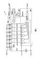
Fig. 1 has shown first embodiment according to semiconductor memory of the present invention.Among the figure, each all forms the signal wire of representing with thick line by a plurality of.Indicate outside entry terminal at the dicyclo that the left side of figure shows.With the signal indication negative logic of labelled notation of band prefix "/", and with the signal indication positive logic of the labelled notation of being with suffix " Z ".In ensuing description, can mention signal by using their abbreviations separately; For example, " external timing signal CLK " can be called " CLK signal ", and " chip start signal/CE " can be called "/CE signal ".
The semiconductor memory that forms has the storage unit as DRAM as a pseudo SRAM, also has the interface as SRAM.This pseudo SRAM has one and upgrades control circuit 10, one determinants 12, one command decoders 14, one train of impulses control circuit, 16, one mode initialization control circuits, 18, one train of impulses address counters 20, one timing control circuit 22, one address latch, 24, one address decoders, 26, one memory cell arrays 28, one read/write amplifier 30, one burst transmission register, 32, one data output control circuits 34 and a data input control circuit 36.
Upgrade control circuit 10, comprise a timer, export a update request signal REFZ, be used for the storage unit MC of updated stored cell array 28 with a predetermined period.
Determinant 12 judges which at first arrives in a update request signal REFZ or the access command, and exports a control signal according to the signal that at first arrives.When memory cell array 28 is that a consecutive access (burst accesses) and a read or write are when carrying out continuously, this access command offers pseudo SRAM from the outside.When one chip start signal/CE and one state signal of the address/ADS showed low level, this access command was recognized.In a burst accesses, input or output a plurality of data in an access command (burst access operation) lining.
When judging first arrival of update request signal REFZ, a commencing signal REFS1 and a useful signal ACTZ are upgraded in determinant 12 outputs one.When judging first arrival of access command, determinant 12 outputs one useful signal ACTZ.Provide chip start signal/CE and state signal of the address/ADS by a chip enable terminal and an address state terminal respectively.When address status signal/ADS showed low level, pseudo SRAM came into force the address signal ADD that is provided to its there.On the contrary, when address status signal/ADS showed high level, pseudo SRAM made the address signal ADD that is provided to its there invalid.Should be understood that the row and column address of address signal ADD is to provide simultaneously because pseudo SRAM has the SRAM interface.
When address status signal/ADS shows low level, command decoder 14 decoding chip enabling signal/CE, output enabling signal/OE and writes enabling signal/WE (each in them generally also will be known as " command signal CMD "), and to timing control circuit 22, data output control circuit 34, data input control circuit 36 or the like output is according to the control signal of decoded result.Writing the startup terminal by an output startup terminal and respectively provides output enabling signal/OE and writes enabling signal/WE.Chip enable, output start and write and start terminal each generally also will be known as " command terminal ".
Train of impulses control circuit 16 receives external timing signal CLK, chip start signal/CE, one train of impulses address advance signal/ADV, one wait for signal LTC from what mode initialization control circuit 18 provided, and export a burst signal BSTZ, train of impulses clock signal BCLK (gating signal), a timing signal and that offers timing control circuit 22 is waited for signal WAIT.External timing signal CLK and train of impulses address advance signal/ADV provide by the preposition terminal of an external clock terminal and a train of impulses address respectively.Waiting signal WAIT waits for that by one terminal outputs to the outside of pseudo SRAM.Train of impulses control circuit 16 moves with output pulse string clock signal BCLK as the first train of impulses control circuit, and moves with output pulse string signal BSTZ as the second train of impulses control circuit.
Mode initialization control circuit 18 receiving chip enabling signal/CE, output enabling signal/OE, write enabling signal/WE, one high byte signal/UB (the first data useful signal), one low byte signal/LB (the second data useful signal), with address signal ADD, and an output waiting signal LTC and a burst length signal BL./ UB and/the LB signal provides by a high byte terminal (the effective terminal of first data) and a low byte terminal (the effective terminal of second data) separately./ UB and/the LB signal is the signal that is used for shielding the part of read and write data.
Mode initialization control circuit 18 be used for setting pseudo SRAM operational mode circuit and have one can be from the mode register of external setting-up.Stand-by period LTC and burst length BL can be set to operational mode.Stand-by period LTC that is provided in advance and burst length BL are respectively as waiting signal LTC and burst length signal BL output.Stand-by period LTC be from an access command (read command) be provided the time be carved into the number of the clock between the moment that first data are output.Burst length BL is the number of times that data are transfused to or import, and it is corresponding to an access command.
Train of impulses address counter 20 is synchronized with the internal address signal IADD that follows address signal ADD from a timing signal for generating of timing control circuit 22.More than 20 generation of train of impulses address counter lacked one internal address signal IADD than the burst length of representing with burst length signal BL.Train of impulses address counter 20 when receiving the high level of train of impulses address advance signal/ADV, stops the counting operation.Address signal ADD provides by End of Address.
Timing control circuit 22 is received from determinant 12, command decoder 14, the control signal of train of impulses control circuit 16 or the like, and the output timing signal is with the gating pulse location counter 20 of ploughing, address latch 24, address decoder 26, the operation of read/write amplifier 30 or the like.
Address latch 24 is synchronized with address latch signal ELAT latch address signal ADD, also is synchronized with address latch signal ILAT and latchs internal address signal IADD, and latch signal is outputed to address decoder 26.
The address signal that address decoder 26 decodings are latched by address latch 24, and output signal is with the storage unit MC in the select storage unit array 28.Especially, address decoder 26 is used for selecting a word line WL according to address signal output word-line signal, and it will be described below and the column line signal, is used for opening the row switch SW, and it also will be described below.
Memory cell array 28 has a plurality of variable storage unit MC that are arranged in the matrix; A plurality of word line WL that are connected with storage unit MC; A plurality of bit line BL that also are connected with storage unit MC; A plurality of sensor amplifier SA that are connected with bit line BL; The row switch SW of a plurality of connection bit line BL and read/write amplifier 30.Storage unit MC, identical with the storage unit of a typical DRAM, each all has one and is used for capacitor that data are kept as electric charge and have a transmission transistor that is distributed between a capacitor and the associated bit line BL.The grid of each transmission transistor are connected with an associated word line WL.
The row switch SW is categorized into corresponding to the first row switch group of/UB signal with corresponding to the secondary series switch group of/LB signal.During a train of impulses write operation, only when/UB signal shows low level, the first series switching response address signal and opening.In this train of impulses write operation, only when/LB signal shows low level, the second series switching response address signal and opening.That is to say that write data is by the shielding of control row switch SW.
In fact, response/UB and/the LB signal, timing control circuit 22 activates address decoders 26, therefore its output array selecting signal CL controls the operation of the first and second row switch groups.Before being transferred to the row switch SW, the write data that data I/O terminal D Q receives to carry out write data shielding control.Therefore, write data shielding control can easily be carried out.
Be synchronized with a sense amplifier enabling signal RAEN, read/write amplifier 30 outputs to data bus DB to the parallel transmission certificate from memory cell array 28.Be synchronized with a write amplifier enabling signal WAEN, read/write amplifier 30 outputs to memory cell array 28 to the concurrent write data that train of impulses transmission register 32 provides.
Burst transmission register 32 has a plurality of data registers (DT0, DT1 and other) and is used for preserving data.Burst transmission register 32 makes the parallel transmission certificate from read/write amplifier 30 be transformed into serial data, and is synchronized with train of impulses clock signal BCLK, and serial data is outputed to a common data bus CDB.Burst transmission register 32 also is transformed into parallel data to the serial write data from common data bus CDB, and is synchronized with train of impulses clock signal BCLK parallel data is outputed to read/write amplifier 30.
Data output control circuit 34 is activated in a read operation, by output buffer the read data on the common data bus CDB is outputed to data I/O terminal D Q.Data I/O terminal D Q is made up of sixteen bit.When high byte signal/UB shows low level, the high eight-bit of data output control circuit 34 these sixteen bit read datas of output.When low byte signal/UB showed low level, data output control circuit 34 was exported low eight of these sixteen bit read datas.Data I/O terminal D Q is by forming corresponding to eight the first data terminal group UDQ of/UB signal with corresponding to eight the second data terminal group LDQ of/LB signal.
Data input control circuit 36 is activated in a write operation, receives write data by data I/O terminal D Q, and the data that receive are outputed to common data bus CDB.Burst transmission register 32, data output control circuit 34 and data input control circuit 36 are used for inputing or outputing continuously a plurality of data as data input/output circuit operation.
Fig. 2 has shown the details of the determinant 12 shown in Fig. 1.
Determinant 12 has one and upgrades judgment part 12a, and one upgrades retaining part 12b, and an order produces a part 12c and an access retaining part 12d.
Part 12a is judged in renewal with a rest-set flip-flop, between the low period of useful signal ACTZ, moves, and which first arrival among a judgement update request signal REFZ or the access signal ACSZ.Access signal ACSZ be an indication/CE and/signal of the OR logic (negative logic) of ADS signal.That is to say, when/CE or/the ADS signal change is during to low level, the providing of access command is found and the ACSZ signal is output.Upgrade judgment part 12a, when judging first arrival of REFZ signal, cause a renewal enabling signal REFENZ to change into high level.Upgrade judgment part 12a, when judging first arrival of ACSZ signal, keeping upgrading enabling signal REFENZ is low level.
When upgrading enabling signal REFENZ demonstration low level or burst signal BSTZ demonstration high level, upgrade retaining part 12b and keep update request signal REFZ.A trailing edge that is synchronized with burst signal BSTZ keeps update request signal REFZ as upgrading commencing signal REFS1 and upgrading commencing signal REFS2 output as one.When upgrading enabling signal REFENZ and show high level and further when burst signal BSTZ showed low level, response update request signal REFZ upgraded retaining part 12b output renewal commencing signal REFS1 and REFS2.Be synchronized with a renewal stop signal RSTPZ who when upgrading EO, exports, upgrade retaining part 12b and stop output renewal enabling signal REFS1.
Burst signal BSTZ is the signal in (during the train of impulses read or write) output during the burst access operation.That is to say, according to the present invention, in train of impulses operation, update request is not lost but has been saved, and (before the finishing of the train of impulses operation of pseudo SRAM) carried out corresponding to the renewal that keeps update request and operated after the train of impulses operation of memory cell array 28.Therefore, can shorten from train of impulses and operate the time of upgrading between the operation beginning, therefore can improve message transmission rate.
A commencing signal REFS2 or an access commencing signal ACSS are upgraded in response, and order produces part 12c output useful signal ACTZ.The output of useful signal ACTZ allows burst access operation or upgrades operation to obtain carrying out.
When effective signal ACTZ shows a low level, response access signal ACSZ, access retaining part 12d output access commencing signal ACSS.Receive as access retaining part 12d between the high period of effective signal ACTZ under the situation of access signal ACSZ, it is not lost but keeps access signal ACSZ, and the trailing edge that is synchronized with useful signal ACTZ, it is keeping access signal ACSZ to export as access enabling signal ACSS.Usually, during burst access operation, when memory cell array 28 operation, there is not new access command to cause to be used for the request of access memory cell array 28 to be provided.Therefore, when effective signal ACTZ is in relation to when upgrading operation and being output, carry out the maintenance of access signal ACSZ.
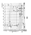
Fig. 3 has shown a kind of operation of the determinant 12 shown in Fig. 2.Fig. 3 has shown that and then update request receives an access command and a kind of situation of taking place.In other words, after a train of impulses read operation, carry out one and upgrade operation.In this example, read the stand-by period to be set to " 4 ", and burst length is set to " 4 ".
At first, be synchronized with the rising edge of zero CLK signal, provide address signal ADD (A0) and/ADS ,/CE and/OE signal (Fig. 3 (a)).In other words, provide a read command.Response/ADS and/the CE signal, determinant 12 output one access signal ACSZ (Fig. 3 (b)).
After access signal ACSZ is output, export a update request signal REFZ (Fig. 3 (c)).Upgrade judgment part 12a and judge first arrival of ACSZ signal, and keep upgrading enabling signal REFENZ in low level.Upgrade the low level that retaining part 12b receives the REFENZ signal, and before the beginning of upgrading operation, keep update request signal REFZ always, shown in the dotted line among the figure (Fig. 3 (d)).
Access retaining part 12d receives ACSZ signal and output access commencing signal ACSS.Order produces part 12c and receives the ACSS signal and export a useful signal ACTZ (Fig. 3 (e)).The ACTZ signal becomes high level and causes memory cell array 28 to become an available state ACTV from a standby attitude STBY.
The train of impulses control circuit 16 that shows among Fig. 1 is received an access command and is exported a burst signal BSTZ (Fig. 3 (f)) and a wait signal WAIT (Fig. 3 (g)).This system comprises pseudo SRAM, and receiving waiting signal WAIT does not have read data to export from pseudo SRAM with detection, and this system for example can another device of access.Therefore, improved the utilization factor of this system bus.
Then, the start bursts read operation, and the first read data D0 and D1 are output to data bus DB (Fig. 3 (h)).Then, finished the read operation of memory cell array 28, and output read data D2 and D3.Train of impulses control circuit 16 causes burst signal BSTZ to change into low level (Fig. 3 (i)).
After read data D2 and D3 were output, memory cell array 28 was de-energized.The trailing edge that is synchronized with burst signal BSTZ, enabling signal REFS1 and REFS2 are upgraded in the renewal retaining part 12b output of determinant 12, are used for starting upgrading operating (Fig. 3 (j)).Therefore, after the operation of memory cell array 28, need not wait for from the read data D2 of burst transmission register 32 and the output of D3 and finishing, upgrade commencing signal REFS1 and REFS2 and be output.Originally, before the output of read data is finished, do not use the renewal of data bus DB to operate the utilization rate that can improve data bus DB.Especially, can receive next access command with more early time.
Enabling signal REFS2 is upgraded in response, and useful signal ACTZ changes into high level once more, and this causes carrying out upgrading operates (Fig. 3 (k)).In other words, when read data D2 and D3 just had been transferred to data I/O terminal D Q, the state of memory cell array 28 became refresh mode REF.
Be synchronized with and upgrade finishing of operation, stop signal RSTPZ is upgraded in output one, and upgrades enabling signal REFS1 and useful signal ACTZ becomes their low levels (Fig. 3 (l), (m)) separately.Then, the state of memory cell array 28 becomes standby attitude STBY.Then ,/CE and/the OE signal caused showing their high level separately, caused finish (Fig. 3 (n)) of train of impulses read operation.
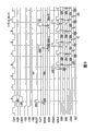
Fig. 4 is the timing diagram that shows another operation of determinant 12.Omitted operation detailed description corresponding to the same operation of Fig. 3.Fig. 4 has shown that a update request occurs near receiving access signal a kind of situation before.That is to say, carry out one prior to a train of impulses read operation and upgrade operation.In this example, read the stand-by period to be set to " 4 ", and burst length is set to " 4 ".
At first, export a update request signal REFZ (Fig. 4 (a)).Upgrade judgment part 12a and judge first arrival of update request signal REFZ, and cause upgrading enabling signal REFENZ and become high level (Fig. 4 (b)).At this moment, because memory cell array 28 is in a standby attitude STBY, a burst signal BSTZ is not output.Therefore, upgrade retaining part 12b and receive REFENZ signal and output renewal enabling signal REFS1 and REFS2 (Fig. 4 (c)).
After this, be synchronized with the rising edge of the 0th CLK signal, provide address signal ADD (A0) and/ADS ,/CE and/the OE signal, and an access signal ACSZ becomes high level (Fig. 4 (d)).Enabling signal REFS2 is upgraded in response, and order produces part 12c and exports a useful signal ACTZ (Fig. 4 (e)).Then, carry out the renewal operation.When upgrading the beginning of operating period and valid period, one waits for that signal WAIT becomes high level (Fig. 4 (f)).The detailed description of waiting signal WAIT will be carried out with reference to Fig. 6 below.
Access retaining part 12d receives the high level of ACTZ signal and keeps ACSZ signal (Fig. 4 (g)).The trailing edge that is synchronized with the ACTZ signal, access retaining part 12d output is corresponding to the ACTZ signal of finishing (Fig. 4 (h)) that upgrades operation.The ACTZ signal change is that high level causes memory cell array 28 directly to become available state ACTV and do not experience standby attitude STBY from refresh mode REF.Therefore, the train of impulses read operation can earlier begin.
After this, be similar to Fig. 3, carry out the train of impulses read operation, and output read data D0-D3 (Fig. 4 (i)).
Fig. 5 is the timing diagram that shows another operation of determinant 12.Omitted detailed description corresponding to the operation of the same operation of Fig. 3.Fig. 5 shown when a complete pulse string pattern being defined as operator scheme, and and then a update request receives an access signal and a kind of situation of taking place.Here " complete pulse string pattern (integrated pattern function) " is a kind of like this operational mode, wherein between the low period of/CE signal, responds an access command, and data are by output continuously (or input).
In this complete pulse string pattern, train of impulses address counter 20 shown in Figure 1 produces internal address signal IADD continuously between the low period of/CE signal.Especially, after the internal address signal IADD corresponding to the word line WL that selects produces continuously, produce internal address signal IADD continuously corresponding to adjacent word line WL.In other words, at complete pulse string run duration, the selection of word line WL is converted.
Among the figure, corresponding to read data Dn-3, Dn-2, the word line WL of Dn-1 and Dn with corresponding to read data D0, D1, the word line WL of D2 and D3 is different.That is to say that during the 8th clock period, the selection of word line WL is converted.When word line WL is converted, carries out one and upgrade operation.In Fig. 5, be identical, and so omitted their detailed description with the operation with the same reference numerals indication among the operation of reference number (a) to (m) indication and Fig. 3.
During can not exporting read data owing to the conversion of word line WL, signal WAIT (Fig. 5 (n)) is waited in output one.
In order to change word line WL, determinant 12 that shows in Fig. 1 and train of impulses control circuit 16 activate burst signal BSTZ and the useful signal ACTZ (Fig. 5 (o)) that once was de-energized again.Then, carry out the train of impulses read operation of the storage unit MC that is connected with the word line WL that reselects.
Fig. 6 has shown the details of the train of impulses control circuit 16 shown in Fig. 1.
Train of impulses control circuit 16 has one or seven bit shift register 16a; Be used for repeatedly exporting a combinational circuit 16b according to the train of impulses clock signal BCLK of burst length BL; Be used for before output pulse string clock signal BCLK, continuing the flip-flop circuit 16c that signal WAIT1 is waited in output one; With first-class circuit 16d to be controlled.Label among Fig. 6 " DLY " and " PLS " represent a delay circuit respectively, another delay circuit and a pulse series generator.
When not having data to be input to during the burst access operation or when data I/O terminal D Q exported, signal WAIT2 was waited in wait control circuit 16d output one.For example, when the selection at complete pulse string run duration word line WL was converted, waiting signal WAIT2 was output.Outputing to the waiting signal WAIT that waits for terminal is the OR logic of waiting signal WAIT1 and WAIT2.
Fig. 7 has shown a kind of operation of the train of impulses control circuit 16 shown in Fig. 6.In this example, the situation that stand-by period in the mode register of the mode initialization control circuit 18 shown in Fig. 1 is set to " 4 " is below described.Now, in this case, with reference to Fig. 6, at the NAND that receives LTC signal face outdoors, only the NAND door of count pick up signal BCNT3 move as a negative circuit, and other NAND door is exported high level.
At first, provide an access command (in this example, because/ read command that the low level of OE signal causes), and the train of impulses control circuit 16 shown in Fig. 1 causes burst signal BSTZ to become a high level (Fig. 7 (a)).The high level of burst signal BSTZ has been cancelled the replacement of shift register 16a.Be synchronized with external timing signal CLK, shift register 16a causes count signal BCNT1-4 result to become high level (Fig. 7 (b)).
The rising edge that is synchronized with count signal BCNT1 is provided with flip-flop circuit 16c, and waiting signal WAIT1 becomes high level (Fig. 7 (c)).
Be synchronized with the rising edge (Fig. 7 (d)) of count signal BCNT3, an enabling signal BCNTEN becomes a high level.The high level replacement flip-flop circuit 16c of enabling signal BCNTEN, and waiting signal WAIT1 becomes a low level (Fig. 7 (e)).
The high level of enabling signal BCNTEN causes train of impulses clock signal BCLK to be synchronized with external timing signal CLK output (Fig. 7 (f)).Train of impulses clock signal BCLK (gating signal) is output the number of times corresponding to the burst length BL that is provided with in the mode register.Then, read data is synchronized with train of impulses clock signal BCLK and is output to data I/O terminal D Q.
Be synchronized with the 6th external timing signal CLK, train of impulses control circuit 16 causes burst signal BSTZ to become low level (Fig. 7 (g)).That is to say, according to the time interval of output pulse string clock signal BCLK, output pulse string signal BSTZ.The low level replacement shift register 16a of burst signal BSTZ causes count signal BCNT1-4 to become low level (Fig. 7 (h)).
The low level of count signal BCNT3 causes enabling signal BCNTEN to become low level, and this causes the output of train of impulses clock signal BCLK to stop (Fig. 7 (i)).Therefore, according to the stand-by period LTC that in mode register, is provided with, the output of beginning read data, and read data is output the number of times (Fig. 7 (j)) corresponding to burst length BL.
Fig. 8 has shown a kind of method to set up of the mode register of the mode initialization control circuit 18 shown in Fig. 1.
The setting of mode register is by default order CMD (CMD1, CMD2, CMD3 are provided toward the there for four times continuously, CMD4) and a default address AD D (CODE1, CODE2, CODE3 CODE4) and then provides pre-set code CODE5 and CODE6 to End of Address and carries out.According to code CODE5 burst length BL is set, and stand-by period LTC is set according to code CODE6.That is to say that mode register receives code CODE5 and the CODE6 conduct is provided with pattern, is used for being provided with operational mode.For example, operational mode is set to an Eight characters pulse string mode when code CODE5 is sexadecimal 0; And it is set to a complete pulse string pattern during sexadecimal 3 when code CODE5.
Fig. 9 has shown the read operation during the complete pulse string pattern in pseudo SRAM described above.
At first, be synchronized with the rising edge of the 0th CLK signal, provide address signal ADD (An) and/ADS ,/CE and/OE signal (Fig. 9 (a)).Timing control circuit 22 outputs one address latch signal ELAT shown in Fig. 1 is used for latching the address signal ADD (Fig. 9 (b)) that provides from the outside.Be synchronized with address latch signal ELAT, address latch 24 latch address signal ADD (An) (Fig. 9 (c)).
Then, timing control circuit 22 output one sense amplifier enabling signal RAEN (Fig. 9 (d)).Sense amplifier enabling signal RAEN activates read/write amplifier 30, causes parallel transmission to output to data bus DB0 and DB1 (Fig. 9 (e)) according to D0 and D1.Be synchronized with train of impulses clock signal BCLK, parallel transmission is converted to serial data according to D0 and D1 by the data register of burst transmission register 32, and outputs to common data bus CDB continuously.Then, be synchronized with clock signal clk, read data D0 and D1 are from data I/O terminal D Q output (Fig. 9 (f)).
Then, timing control circuit 22 output one address latch signal ILAT (Fig. 9 (g)).Be synchronized with address latch signal ILAT, address latch 24 latchs internal address signal IADD (An+1) (Fig. 9 (h)).Then, with top similar mode, output is corresponding to read data D2 and the D3 (Fig. 9 (i)) of internal clock signal IADD.
After this, timing control circuit 22 continuous OPADD latch signal ILAT (Fig. 9 (j)), and, export read data (Fig. 9 (k)) continuously according to the internal address signal IADD that train of impulses address counter 20 produces.
Figure 10 has shown the write operation during the complete pulse string pattern in pseudo SRAM described above.
At first, be synchronized with the rising edge of the 0th CLK signal, provide address signal ADD (An) and/ADS ,/CE and/WE signal (Figure 10 (a)).Timing control circuit 22 outputs one address latch signal ELAT shown in Fig. 1 is used for latching the address signal ADD (Figure 10 (b)) that provides from the outside.Be synchronized with address latch signal ELAT, address latch 24 latch address signal ADD (An) (Figure 10 (c)).
In write operation, be synchronized with each CLK signal rising edge separately, write data is provided by this way continuously: continuous the providing of write data is provided the rising edge that is synchronized with the CLK signal, at this moment, receives access command (Figure 10 (d)).Be synchronized with train of impulses clock signal BCLK, the data register of burst transmission register 32 keeps the write data from common data bus CDB continuously, and the data transmission that keeps is arrived data bus DB0 and DB1.That is to say that the serial write data on the common data bus CDB is converted into concurrent write data (Figure 10 (e)).
Be synchronized with a write amplifier enabling signal WAEN, read/write amplifier 30 is writing into memory cell array 28 (Figure 10 (f)) from the write data of data bus DB0 and DB1.
Then, be similar to Fig. 9, be synchronized with address latch signal ILAT, latch internal address signal IADD (Figure 10 (g)).Then, write data D3, D4, D5 and other are write among the storage unit MC corresponding to internal address signal IADD (Figure 10 (h)) in succession.
Figure 11 has shown the function of train of impulses address advance signal/ADV.
Provide/the feasible output that temporarily stops a burst access operation and keep read data of ADV signal.For example, if being synchronized with the rising edge of the 4th clock signal clk, a high level of/ADV signal is provided, burst access operation is temporarily stopped, and is synchronized with the next clock period and the read data D1 that exports not only is held in the 4th clock period but also in the 5th clock period.That is to say that the internal operation that causes pseudo SRAM that provides of/ADV signal changes after a clock period.
Figure 12 has shown the function of low byte signal/LB and high byte signal/UB during a train of impulses read operation.Among the figure, in order to understand better, common data bus CDB is described as the bus of separation: corresponding to the LCDB of/LB signal with corresponding to the UCDB of/UB signal.
/ LB signal be such signal it be provided so that data low eight effectively, and/the UB signal be such signal it be provided so that the high eight-bit of data is effective.According to this embodiment, in read operation, if/ rising edge that a high level of LB signal (or/UB signal) is synchronized with a clock signal clk is provided, the read data that will be synchronized with next clock period output output that is under an embargo.That is to say that the output buffering in the data output control circuit 34 shown in Fig. 1 is de-energized, and therefore causes data I/O terminal D Q to enter a high impedance state.
Figure 13 has shown the function of low byte signal/LB and high byte signal/UB during a train of impulses write operation.Equally, in the figure, in order to understand better, common data bus CDB is described as the bus of separation: corresponding to the LCDB of/LB signal with corresponding to the UCDB of/UB signal.Equally, in order to understand better, data bus DB0 is described as the bus of separation: corresponding to the LDB0 of/LB signal with corresponding to the UDB0 of/UB signal.Equally, data bus DB1 is described as the bus of separation: corresponding to the LDB1 of/LB signal with corresponding to the UDB1 of/UB signal.
According to this embodiment, in write operation, if/ rising edge that a high level of LB signal (or/UB signal) is synchronized with a clock signal clk is provided, and the write data that is synchronized with this clock signal clk output is de-energized.Especially, when showing a high level, (LCL1 UCL1) does not export corresponding array selecting signal CL for LCL0, UCL0, so that the row switch SW is not opened when/LB signal (or/UB signal).Therefore, do not write into storage unit MC corresponding to the write data of the high level of/LB signal (or/UB signal).
For example ,/the UB signal Synchronization shows a high level (B1) in the 0th clock signal clk./ LB signal Synchronization shows a high level (C1) in first clock signal clk.Therefore, corresponding array selecting signal UCL0 and LCL1 do not export, and the write data that is transferred to data bus LDB1 and UDB0 is not write into storage unit MC.
In first embodiment described above, when a update request signal REFZ and an access request mutual conflict is provided the time, in operation or the burst access operation which determinant 12 decision upgraded and at first carried out.Therefore, in pseudo SRAM, upgrade and burst access operation can be carried out and not overlapping continuously.Because burst access operation can be carried out not with upgrade operating collision, read data can be with a high speed output, and write data can be with a high speed input.That is to say, can improve message transmission rate.
What form in determinant 12 is to upgrade retaining part 12b to be used for keeping update request signal REFZ during burst access operation.Therefore, when burst access operation is carried out prior to upgrading operation, can prevent that update request signal REFZ from losing.What form in determinant 12 equally is that access retaining part 12d is used for keeping an access command during burst access operation.Therefore, when upgrading operation and carry out, can prevent that access request from losing prior to burst access operation.
Upgrade the finishing of output of retaining part 12b response impulse string signal BSTZ and export renewal commencing signal REFS1 and REFS2.Therefore, when burst access operation is at first carried out, can shorten from burst access operation to the time of upgrading the operation beginning.As a result, next access command can earlier provide, and therefore can improve message transmission rate.
Upgrade retaining part 12b and also export and upgrade commencing signal REFS1 and REFS2, and needn't wait for finishing from the output of the read data of burst transmission register 32.Therefore, the train of impulses run duration upgrades operation and can start, and therefore can further improve message transmission rate.
In service at the complete pulse string, when the selection of word line WL is changed, upgrade retaining part 12b output and upgrade commencing signal REFS1 and REFS2.(when conversion word line WL) carries out to upgrade to operate and can make the effect minimum of operating with the renewal of external access interference when the train of impulses outage.As a result, even be inserted into the complete pulse string when in service, can prevent that message transmission rate from reducing when upgrading operation.
The address signal ADD that response provides according to access command, train of impulses address counter 20 produce continuously for the essential internal address signal IADD of train of impulses operation.In the inner effect of tiltedly moving that can reduce address signal for the essential address signal of train of impulses operation that produces of pseudo SRAM.Therefore, the cycle of operation can be independent of the address tiltedly to be moved and is shortened, and therefore can further improve message transmission rate.
Form and wait for that terminal is with the invalid waiting signal WAIT of output expression data I/O terminal D Q.Therefore, comprise that the system of pseudo SRAM can be with an optimum timing according to waiting signal WAIT access pseudo SRAM.For example, be used for the CPU or the like of management system can access between the period of output of waiting signal WAIT one different equipment.As a result, can improve the utilization rate of system bus.
According to/UB and/input of LB signal write data and the output conductively-closed of read data.Therefore, even when the bit width of data-signal DQ is very big, the effective write and read data taken signal DQ of the system that comprises pseudo SRAM.
In write operation,, shielded write data by turning off the row switch that moves in the slow relatively time.Therefore, can easily carry out the shielding control of write data.
Pattern is provided with the signal of control circuit 18 in address and continuous four the reception logic of propositions values of command terminal, receives signal CODE5 and the CODE6 that offers End of Address then, is used for being provided with as signalization and reads stand-by period LTC and burst length BL.Necessity that provides any special-purpose terminal to be used for being provided with operational mode has been provided for this.
Train of impulses run duration, read data are transferred to after the data register of burst transmission register 32, and memory cell array 28 is de-energized.The quick de-energisation of memory cell array 28 allows the operation of response one update request or next access request earlier to begin during the train of impulses read operation.As a result, can improve message transmission rate.
Figure 14 has shown second embodiment according to semiconductor memory of the present invention.In this embodiment, represent with same reference number corresponding to the element of similar elements in first embodiment, and their detailed descriptions have been omitted.
According to present embodiment, form timing control circuit 22, read/write amplifier 30 and burst transmission register 32 that a timing control circuit 38, one read/write amplifiers 40 and a burst transmission register 42 replace first embodiment respectively.A data bus DB who connects read/write amplifier 40 and burst transmission register 42 has the bit width identical with common data bus CDB.Those of other structure of present embodiment and first embodiment are identical.
In train of impulses operating period, be synchronized with each clock signal clk rising edge separately, timing control circuit 38 output sense amplifier enabling signal RAEN or write amplifier enabling signal WAEN.Burst transmission register 42 by common data bus CDB directly the read data transmission that provides by read/write amplifier 40 to data output control circuit 34.That is to say that read data is changed without parallel-to-serial.Burst transmission register 42 directly outputs to read/write amplifier 40 to the write data that is provided by data input control circuit 36 by data bus DB.That is to say that write data changes without undergoing serial-to-parallel.
Figure 15 has shown a complete pulse string read operation of the pseudo SRAM shown in Figure 14.Detailed description corresponding to the operation of the same operation of first embodiment (Fig. 5) has been omitted.
In Figure 15, and then receive an access command, produce a update request.That is to say, after a read operation, carry out one and upgrade operation.In this embodiment, read stand-by period LTC and be set to " 4 ".
At first, be synchronized with the rising edge of the 0th CLK signal, a read command is provided, and the determinant 12 output access signal ACSZ (Figure 15 (a)) that show among Fig. 2.The renewal judgment part 12a of determinant 12 receives a update request signal REFZ after read command is provided.Therefore, upgrade enabling signal REFENZ and be maintained at low level (Figure 15 (b)).Order produces part 12c response access signal ACSZ output useful signal ACTZ.(Figure 15 (c)).Useful signal ACTZ becomes high level and causes memory cell array 28 to become available state ACTV from standby attitude STBY.
Then, a burst signal BSTZ becomes a high level, and waiting signal WAIT shows a high level in a Preset Time.Timing control circuit 38 is synchronized with the 3rd to the 6th clock signal clk rising edge output sense amplifier enabling signal RAEN (Figure 15 (d)) separately.Train of impulses control circuit 16 is synchronized with the 3rd to the 6th clock signal clk rising edge output pulse string clock signal BCLK (Figure 15 (e)) separately.Then, carry out read operation, and read data Dn-3, Dn-2, Dn-1 and Dn output to data bus DB (Figure 15 (f)) in succession.
In the present embodiment, read/write amplifier 40 is exported read data Dn-3, Dn-2, Dn-1 and Dn according to clock signal clk separately.Therefore, before the 4th read data Dn was transferred to read/write amplifier 40, memory cell array 28 must operation.Therefore, the length in the cycle of available state ACTV is than a middle long clock period (Figure 15 (g)) of first embodiment (Fig. 5).
After the finishing of read operation, carry out and upgrade operation (Figure 15 (h)).Carrying out renewal than a late clock period in first embodiment (Fig. 5) operates.Therefore, also clock period of evening begins the operating next read operation of complete pulse string.Therefore, data transmission rate lower than in the first embodiment (Fig. 5).
Yet the renewal operation between the read operation can provide a data transmission rate that is higher than prior art in the operation of execution train of impulses when starting impulse string operation in pseudo SRAM.
Present embodiment can provide and the identical effect of aforementioned first embodiment.
Figure 16 has shown the 3rd embodiment according to semiconductor memory of the present invention.In this embodiment, represent with same reference number corresponding to the element of similar elements in first embodiment, and their detailed description has been omitted.
According to present embodiment, form a command decoder 44, one train of impulses control circuit 46 (the first train of impulses control circuit), one pattern is provided with the command decoder 14 that control circuit 48 and a burst transmission register 50 replace first embodiment respectively, train of impulses control circuit 16, pattern are provided with control circuit 18 and burst transmission register 32.Those of other structure of present embodiment and first embodiment are identical.
When receiving one by command terminal when reading or writing order, command decoder 44 is exported a read control signal RDZ or a write control signal WRZ respectively.During one read operation, train of impulses control circuit 46 receives read control signal RDZ, calculates clock according to stand-by period signal RLTC with certain number of times, and exports a read pulse string clock signal RBCLK according to burst length BL with certain number of times then.In a write operation, train of impulses control circuit 46 receives write control signal WRZ, calculates clock according to write latency signal WLTC with certain number of times, and exports a write pulse train clock signal WBCLK according to burst length BL with certain number of times then.
Pattern is provided with that control circuit 48 has can be from a mode register of outer setting.Burst length BL reads stand-by period RLTC and write latency WLTC is arranged in the mode register.Be arranged on value in this mode register as a burst length signal BL, one reads stand-by period signal RLTC and a write latency signal WLTC outputs in train of impulses control circuit 46 and the train of impulses address counter 20.Read stand-by period RLTC and be from a read command be provided the time be carved into the number of the clock between the moment that first data are output.More particularly, read stand-by period RLTC and represent during the read operation number from the rising edge of one chip start signal/CE to the clock the output of first data.
Write latency WLTC be from a write order be provided the time be carved into the number of the clock between the moment that first data are transfused to.More particularly, write latency WLTC represents during the write operation number from the rising edge of one chip start signal/CE to the clock the input of first data.Therefore, present embodiment is characterised in that the stand-by period of read and write operation can be provided with independently of each other.
Burst transmission register 50 has a plurality of data registers (DT0, DT1 or the like) that are used for preserving data.Burst transmission register 50 is transformed into serial data to the parallel transmission certificate that is provided by read/write amplifier 30, and is synchronized with read pulse string clock signal RBCLK, and the serial data that changes is outputed to common data bus CDB.Simultaneously, burst transmission register 50 is transformed into parallel data to the serial write data that is provided by common data bus CDB, and is synchronized with write pulse train clock signal WBCLK, and the parallel data that changes is outputed to read/write amplifier 30.
Figure 17 and 18 has shown the details of the train of impulses control circuit 46 shown in Figure 16.Figure 17 has shown a circuit part of train of impulses control circuit 46, it is used for producing read pulse string clock signal RBCLK and waiting signal WAIT during read operation, and Figure 18 has shown a circuit part of train of impulses control circuit 46, and it is used for producing write pulse train clock signal WBCLK during write operation.
Among Figure 17, train of impulses control circuit 46 has a clock generation circuit 46a; One or seven bit shift register 46b; One is used for exporting the combinational circuit 46c of read pulse string signal RBCLK; One is used for exporting the flip-flop circuit 16c of waiting signal WAIT1; First-class circuit 16d to be controlled; Delay circuit DLY; Produce circuit PLS with a train of impulses.Clock generation circuit 46a moves between the low period of chip start signal/CE, and clock signal clk is exported as internal clock signal RCLK1.Clock generation circuit 46a moves as a level detecting circuit, is used for surveying the chip start signal/CE (command signal) that is used as an access command and provides and changes to its significant level (low level).
The shift register 16a of shift register 46b and the combinational circuit 46c and first embodiment is approximate identical with combinational circuit 16b (Fig. 6).Therefore, those operations of the related circuit of the basic operation of shift register 46b and combinational circuit 46c and first embodiment (Fig. 7) are identical.The numeral of representing in the mark of the phase inverter of combinational circuit 46c and dual input NAND door is corresponding to the value of reading stand-by period RLTC.For example, when reading stand-by period RLTC and be set to " 4 ", the NAND door that only is numbered " 4 " is activated.
When showing a low level, an output enabling signal/OE (that is to say, when a RDZ signal shows a high level), combinational circuit 46c output read pulse string clock signal RBCLK, more late corresponding to a number of reading the clock of stand-by period RLTC than providing of one chip start signal/CE, the number of number of times is consistent with a burst length BL.That is to say, shift register 46b and combinational circuit 46c move as an output control circuit together, it measured change to the Preset Time that their significant level begins to count from chip start signal/CE and output enabling signal/OE after, start the output of read pulse string clock signal RBCLK.
Identical in the circuit that is used for producing waiting signal WAIT and first embodiment, and therefore omitted its description.
In Figure 18, the train of impulses control circuit has a clock generation circuit 46d, one or seven bit shift register 46e and be used for exporting a combinational circuit 46f of write pulse train clock signal.When one chip start signal/CE showed low level, clock generation circuit 46d moved so that clock signal clk is exported as internal clock signal WCLK1.Clock generation circuit 46d moves as a level detecting circuit, is used for surveying the chip start signal/CE (command signal) that is used as an access command and provides and changes to its significant level.
Shift register 46e is identical with combinational circuit 46c with the shift register 46b shown in Figure 17 with combinational circuit 46f.Numeral that the mark of the phase inverter of combinational circuit 46f and dual input NAND door is represented and the value of write latency WLTC meet.For example, the NAND door that when write latency WLTC is set to " 4 ", only is numbered " 4 " is activated.
Write and (that is to say when enabling signal/WE shows a low level when one, when a WRZ signal shows a high level), combinational circuit 46f output write pulse train clock signal WBCLK, than the number of the late clock corresponding to write latency WLTC of providing of one chip start signal/CE, the number of number of times is consistent with a burst length BL.That is to say, shift register 46e and combinational circuit 46f move as an output control circuit together, it starts the output of write pulse train clock signal WBCLK after having measured the Preset Time that the significant level that changes to them from chip start signal/CE begins to count.Shift register 46e is identical with related circuit those (Fig. 7) in first embodiment with combinational circuit 46f.
Those of the delay circuit DLY1 of the delay circuit DLY1 of Figure 18 and the time delay of DLY2 and Figure 17 and DLY2 are different.That is to say that preset times described above just is different on the length between the read and write operation.Yet, be to be understood that the delay circuit DLY1 that can be provided with and Figure 17 time delay of the delay circuit DLY1 of Figure 18 and DLY2 is identical with those of DLY2, so that the length of the Preset Time in the read and write described above operation can be the same.
Figure 19 has shown that the pattern shown in Figure 16 is provided with the method to set up of the mode register in the control circuit 48.
The setting of mode register be by provide toward the there for four times continuously a default order CMD (CMD1, CMD2, CMD3, CMD4) and a default address AD D (CODE3 CODE4) and then provides pre-set code CODE5 to End of Address for CODE1, CODE2.That is to say that mode register receives code CODE5 as the signalization that is used for being provided with operational mode.The number of clock period that is used for being provided with mode register is than lacking one in the first embodiment.
In the present embodiment, outside a byte as the address A7-A0 that provides of coding CODE5, low two are used for being provided with burst length BL, and three that follow are used for being provided with and read stand-by period RLTC, and the Senior Three position is used for being provided with write latency WLTC.Read stand-by period RLTC and can be set to eight probable values: " 1 " arrives any one in " 8 ".Write latency WLTC also can be set to eight probable values: " 0 " arrives any one in " 7 ".Therefore, the stand-by period of read and write operation can be provided with independently of one another.In other words, read and write operating period, the train of impulses control circuit 46 shown in Figure 16 can produce the train of impulses clock signal RBCLK and the WBCLK of separate timing.As a result, the availability that has merged the system of pseudo SRAM can improve.
Figure 20 has shown the read operation during the pulse string mode in the pseudo SRAM of the 3rd embodiment.Identical (Fig. 7 to 9) in the basic timing of read operation and first embodiment, and therefore omitted description corresponding to identical operations in first embodiment.In this embodiment, read stand-by period RLTC and be set to " 4 ".
At first, the clock generation circuit 46a shown in Figure 17 is activated by the low level of one chip start signal/CE, to start the output (Figure 20 (a)) of internal clock signal RCLK1.The low level of the low level of chip start signal/CE and an output enabling signal/OE causes a read control signal RDZ to be output (Figure 20 (b)).Be synchronized with second clock signal CLK, this shift register 46b causes a count signal BCNT3 to become a high level (Figure 20 (c)).
Combinational circuit 46c is activated by the high level of read control signal RDZ and count signal BCNT3, so that clock signal clk is exported (Figure 20 (d)) as read pulse string clock signal RBCLK.That is to say, the output of read pulse string clock signal RBCLK begin to be synchronized with the 3rd clock signal clk.
Then, be similar to first embodiment, be synchronized with read pulse string clock signal RBCLK and export read data continuously.The system synchronization that has merged pseudo SRAM receives first read data (Figure 20 (e)) in the rising edge of the 4th clock signal clk.
The startup of the output of the train of impulses address counter 20 shown in Figure 16 by being synchronized with read pulse string clock signal RBCLK receives by a control signal of train of impulses control circuit 46 outputs by timing control circuit 22 and they is added up, and then count value is exported (Figure 20 (f)) as an internal address signal IADD.
Though do not show, be to be understood that combinational circuit 46c always is activated when reading stand-by period RLTC and be set to " 1 ".Therefore, the first read pulse string clock signal RBCLK is synchronized with zero clock signal clk output.Then, allow read data to be synchronized with the time that first clock signal clk is received by system at one, the output read data.
Figure 21 has shown the write operation during the pulse string mode in the pseudo SRAM of the 3rd embodiment.Omitted description corresponding to identical operations (Figure 10) in first embodiment.In this embodiment, write latency WLTC is set to " 4 ".
At first, the clock generation circuit 46d shown in Figure 18 is activated by the low level of one chip start signal/CE, to start the output (Figure 21 (a)) of internal clock signal WCLK1.The low level that the low level of chip start signal/CE and is write enabling signal/WE causes a write control signal WRZ to be output (Figure 21 (b)).Be synchronized with the 3rd clock signal clk, this shift register 46e causes a count signal BCNT4 to become a high level (Figure 21 (c)).
Combinational circuit 46f is activated by the high level of write control signal WRZ and count signal BCNT4, so that clock signal clk is exported (Figure 21 (d)) as write pulse train clock signal WBCLK.That is to say, the output of write pulse train clock signal WBCLK begin to be synchronized with the 4th clock signal clk.
The system synchronization that has merged pseudo SRAM in, for example, the rising edge of the 4th clock signal clk outputs to (Figure 21 (e)) in the pseudo SRAM to first write data.The rising edge that pseudo SRAM is synchronized with the 4th clock signal clk receives this write data, and this write data is transferred to common data bus CDB (Figure 21 (f)).Write data on the common data bus CDB is synchronized with write pulse train clock signal WBCLK and is transferred to a data bus DB (DB0 or DB1).
The startup of the output of the train of impulses address counter 20 shown in Figure 16 by being synchronized with write pulse train clock signal WBCLK is received by a control signal of train of impulses control circuit 46 outputs by timing control circuit 22 and counts, and produces this count value then as an internal address signal IADD (Figure 21 (g)).Then, be synchronized with write pulse train clock signal WBCLK, the write data that is provided in succession is transferred among the data bus DB, and is write among the storage unit MC then.
Though do not show, be to be understood that when write latency WLTC was set to " 0 ", combinational circuit 46f always was activated.Therefore, the first write pulse train clock signal WBCLK is synchronized with zero clock signal clk output.At this moment, allow write data to be synchronized with zero clock signal clk, merged the system output writer data of pseudo SRAM by the time that pseudo SRAM receives at one.
This embodiment described above can be provided in the aforementioned first embodiment similar effects.In addition, because the startup of the output of the input of read data or write data is preset stand-by period RLTC or WLTC than the level change late of chip start signal/CE, the system that has merged pseudo SRAM can easily control pseudo SRAM.That is to say that this system architecture can be simplified.Should be understood that thereby pseudo SRAM causes the level change log-on data I/O operation of chip start signal/CE.Therefore, the present invention not only can be applied in the clock synchronization pseudo SRAM and also can be applied to the asynchronous pseudo SRAM of clock.
Can be according to can and remaining on stand-by period RLTC the mode register and WLTC is provided with the timing of the output that starts read data and starts the timing of the input of write data from outer setting.Therefore, can best stand-by period RLTC and WLTC be set according to system performance.
Mode register can be provided with independently of one another reads stand-by period RLTC and write latency WLTC.Therefore, can stand-by period RLTC and WLTC be set neatly according to system performance, so that system performance can improve.
Figure 22 has shown the 4th embodiment according to semiconductor memory of the present invention.In this embodiment, represent with same reference number corresponding to the element of similar elements in the first and the 3rd embodiment, and their detailed descriptions have been omitted.
According to present embodiment, form a command decoder 44, one train of impulses control circuit 52, one pattern is provided with control circuit 54 and the command decoder 14 of a burst transmission register 50 to replace first embodiment respectively, train of impulses control circuit 16, pattern are provided with control circuit 18 and burst transmission register 32.Those of other structure of present embodiment and first embodiment are identical.Command decoder 44 is identical with the related circuit of second embodiment with burst transmission register 50.
During the read operation, respond a read control signal RDZ and an output enabling signal/OE, train of impulses control circuit 52 produces read pulse string clock signal RBCLK.Simultaneously, during the write operation, respond a write control signal WRZ and and write enabling signal/WE, train of impulses control circuit 52 produces write pulse train clock signal WBCLK.
Pattern is provided with control circuit 54 outputs one a default waiting signal RLTC and the default waiting signal WLTC that writes of reading.
Figure 23 and 24 has shown the details of the train of impulses control circuit 52 shown in Figure 22.Figure 23 shown and is used for during read operation producing the circuit part that read pulse string clock signal RBCLK and waits for the train of impulses control circuit 52 of signal WAIT, and Figure 24 has shown a circuit part of the train of impulses control circuit 52 that is used for producing write pulse train clock signal WBCLK during write operation.
Be provided for the clock generation circuit 46a except output enabling signal/OE replaces chip start signal/CE, the train of impulses control circuit 52 shown in Figure 23 is identical with the related circuit (Figure 17) of the 3rd embodiment.The shift register 46b of train of impulses control circuit 52 and combinational circuit 46c move as an output control circuit together, it measured change to the Preset Time that their significant level begins to count from output enabling signal/OE after, start the output of read pulse string clock signal RBCLK.
Replace chip start signal/CE to be provided for the clock generation circuit 46d except writing enabling signal/WE, the train of impulses control circuit 52 shown in Figure 24 is identical with the related circuit (Figure 18) of the 3rd embodiment.The shift register 46e of train of impulses control circuit 52 and combinational circuit 46f move as an output control circuit together, it starts the output of write pulse train clock signal WBCLK having measured after write the Preset Time that significant level that enabling signal/WE changes to them begins to count.
Figure 25 has shown that the pattern among Figure 22 is provided with the details of control circuit 54.
Mode setting circuit 54 has a mode register 54a and the change-over circuit 54b that are connected with each eight of mode register 54a output A0-A7.Mode register 54a, identical with the mode register of the 3rd embodiment, can burst length BL be set according to the aforementioned method of describing with reference to Figure 19, read stand-by period RLTC and write latency WLTC.
Each of change-over circuit 54b all has a switch SW 1 that is connected with a supply voltage VDD; A switch SW 2 that is connected with ground pressure VSS; Independent switch SW 3 that output is connected with mode register 54a.In the manufacture process (wiring process) of pseudo SRAM, switch SW 1, one among SW2 and the SW3 makes its conducting.
Especially, prepare two photomasks that in wiring process, to use in advance.In one in two photomasks, form a wiring figure, it makes each switch SW 3 conduction of change-over circuit 54b, and in another photomask, form a wiring figure, it makes each switch SW 1 and the SW2 conduction of change-over circuit 54b.Then, optionally use photomask to make such product, wherein burst length BL and stand-by period RLTC and WLTC can revise according to the value of mode register 54a, and such product, and wherein burst length BL and stand-by period RLTC and WLTC are defined as a preset value.
Pattern is provided with the switch (SW1, SW2 and SW3) that control circuit 54 forms on the substrate of pseudo SRAM according to the wiring figure according to a photomask that optionally uses, output pulse string length BL and stand-by period RLTC and WLTC in manufacture process.Train of impulses control circuit 52 is to be provided with the stand-by period RLTC of control circuit 54 outputs and the time output pulse string clock signal RBCLK (or WBCLK) that WLTC determines according to burst length BL with from pattern.In other words, the time that train of impulses control circuit 52 is measured corresponding to waiting signal RLTC (or WLTC), it is according to those the magnitude of voltage that is connected with conductive pattern with change-over circuit 54b, and after measurement, begins the output of train of impulses clock signal RBCLK (or WBCLK).
Figure 26 has shown the read operation during the pulse string mode in the pseudo SRAM of the 4th embodiment.In this embodiment, read stand-by period RLTC and be set to " 2 ".Read stand-by period RLTC and be to be activated into the number of the clock of first read data between being output from output enabling signal/OE.
The activation of exporting enabling signal/OE during the 52 response read operations of train of impulses control circuit starts the output (Figure 26 (a)) of internal clock signal RCLK1.Identical during the train of impulses read operation in the basic timing of ensuing operation and the 3rd embodiment (Figure 20), and therefore omitted their description.
Figure 27 has shown the write operation during the pulse string mode in the pseudo SRAM of the 4th embodiment.In this embodiment, write latency WLTC is set to " 2 ".Write latency WLTC is from writing the number that enabling signal/WE is activated into the clock of first read data between being transfused to.
Write the activation of enabling signal/WE during the train of impulses control circuit 52 response write operations, start the output (Figure 27 (a)) of internal clock signal WCLK1.Identical during the train of impulses write operation in the basic timing of ensuing operation and the 3rd embodiment (Figure 21), and therefore omitted their description.
Embodiments of the present invention described above can provide and the aforementioned first and the 3rd embodiment similar effects.In addition, owing to can stand-by period RLTC and WLTC be set by optionally using photomask, they can be provided with according to the product specification (running frequency or the like) of the semiconductor memory of will deliver.Using according to the selectivity of photomask, making by identical manufacturing step and be used as at the pseudo SRAM that has enough limits on the running frequency under the situation of the different product delivery with different running frequencies, this embodiment is especially favourable.
Figure 28 has shown the 5th embodiment according to semiconductor memory of the present invention.In this embodiment, represent with same reference number corresponding to the element of similar elements in the first and the 3rd embodiment, and their detailed descriptions have been omitted.
According to present embodiment, form a command decoder 44, one train of impulses control circuit 46, one pattern is provided with the command decoder 14 that control circuit 56 and a burst transmission register 50 replace first embodiment respectively, train of impulses control circuit 16, pattern are provided with control circuit 18 and burst transmission register 32.Those of other structure of present embodiment and first embodiment are identical.Command decoder 44, train of impulses control circuit 46 is identical with the related circuit of second embodiment with burst transmission register 50.
Figure 29 has shown that pattern is provided with the details of control circuit 56.
Mode setting circuit 56 has a mode register 56a and is used for each eight the change-over circuit 56b that export A0-A7 of receiving mode register 56a.Mode register 56a, identical with the mode register of the 3rd embodiment, can with reference to Figure 19 burst length BL be set according to aforesaid method, read stand-by period RLTC and write latency WLTC.
Each of change-over circuit 56b all has two fuse circuit 56c, has all designed one data in they each.Fuse circuit 56c, it by one pseudo SRAM open electricity the time temporary transient trigger signal STTZ (the opens electric reset signal) initialization that shows a high level, according to the procedure condition output logic value of fuse FS1 and FS2.When fuse FS1 has been programmed (under a cut-out condition), signal V1 and/V1 changes to low and high level respectively.When fuse FS1 also is not programmed (under disconnected condition), signal V1 and/V1 changes to height and low level respectively.Similarly, when fuse FS2 has been programmed (under a cutting condition), signal V2 and/V2 changes to low and high level respectively.When fuse FS2 also is not programmed (under disconnected condition), signal V2 and/V2 changes to height and low level respectively.
According to present embodiment, making such product, burst length BL wherein, read waiting signal RLTC and write under the situation that waiting signal WLTC can be modified according to the value that is arranged among the mode register 56a, the fuse FS1 of each of mode setting circuit 56b and FS2 are placed in the disconnected state in the test process.At this moment, in each mode setting circuit 56b, a NAND door, it is the lower of two NAND doors shown in Figure 29, exports a low level, it opens a cmos transmission gate.Then, be arranged on value among the mode register 56a, read stand-by period RLTC and write latency WLTC output as burst length BL.
Pulse string length BL, the value of reading stand-by period RLTC and write latency WLTC is fixed under the situation of preset value, and fuse FS1 or the FS2 of each mode setting circuit 56b breaks in the manufacture process.At this moment, cmos transmission gate is closed, so the output conductively-closed of mode register 56a.Fuse FS2 is continuous if fuse FS1 is disconnected, exports a ground and presses VSS.On the contrary, fuse FS1 is continuous if fuse FS2 is disconnected, exports a supply voltage VDD.That is to say that each mode setting circuit 56b exports a high or low pressure according to the program conditions of fuse FS1 and FS2.Like this, make wherein burst length BL, read the product that stand-by period RLTC and write latency WLTC are fixed on preset value.
Therefore, pattern be provided with control circuit 56 according to the program conditions of fuse FS1 and FS2 pulse string length BL, read stand-by period RLTC and write latency WLTC and output to train of impulses address counter 20 and train of impulses control circuit 46.In other words, train of impulses control circuit 46 is measured time corresponding to stand-by period RLTC (or WLTC) according to the program conditions of fuse FS1 and FS2, and the output of start bursts clock signal RBCLK (or WBCLK) after measurement.
Train of impulses read and write operation is identical with in first embodiment those in the present embodiment, and so omitted their description.
Embodiments of the present invention described above can provide and the aforementioned first and the 3rd embodiment similar effects.In addition, can stand-by period RLTC and WLTC be set by programmable fuse FS1 and FS2.Therefore, according to FS2 the aforementioned Preset Time consistent with the actual performance of the pseudo SRAM of making being set as the maximum running frequency design fuse FS1 that estimates in the probing test.Actual performance on each comfortable running frequency according to them is used as under the situation of different product classification and delivery the pseudo SRAM by identical photomask and identical manufacturing step manufacturing, and this embodiment is especially favourable.
Aforementioned first and second embodiments are described as such example, and wherein the train of impulses stand-by period TC that reads run duration is set to " 4 ".Yet, the invention is not restricted to these embodiments.Stand-by period LTC can be set to an optimal value according to the clock period.
The present invention is described as such example, wherein receives the burst length BL be used for being provided with in the mode register and pattern CODE5 and the CODE6 of stand-by period LTC at End of Address.Yet, the invention is not restricted to these embodiments.For example, can replace utility command or data terminal with receiving mode CODE5 and CODE6.
The the aforementioned the three, the four and the 5th embodiment is described as such example, wherein read and write stand-by period RLTC and the separate setting of WLTC.Yet, the invention is not restricted to these embodiments.For example, as shown in Figure 30, the position A4-A2 of mode register can be identical with WLTC with read and write stand-by period RLTC.Perhaps, write latency WLTC can be provided with always than reading stand-by period RLTC little " 1 ".Under such situation, the number of the position of mode register can reduce.
The invention is not restricted to above embodiment, and do not leave the spirit and scope of the present invention, can carry out various modifications.On part or all of parts, can carry out any improvement.