JP4080892B2 - Multi-bit prefetch output data path - Google Patents
Multi-bit prefetch output data path Download PDFInfo
- Publication number
- JP4080892B2 JP4080892B2 JP2002586351A JP2002586351A JP4080892B2 JP 4080892 B2 JP4080892 B2 JP 4080892B2 JP 2002586351 A JP2002586351 A JP 2002586351A JP 2002586351 A JP2002586351 A JP 2002586351A JP 4080892 B2 JP4080892 B2 JP 4080892B2
- Authority
- JP
- Japan
- Prior art keywords
- output
- signal
- data
- data bits
- enable signal
- Prior art date
- Legal status (The legal status is an assumption and is not a legal conclusion. Google has not performed a legal analysis and makes no representation as to the accuracy of the status listed.)
- Expired - Fee Related
Links
Images


Classifications
-
- G—PHYSICS
- G11—INFORMATION STORAGE
- G11C—STATIC STORES
- G11C7/00—Arrangements for writing information into, or reading information out from, a digital store
- G11C7/10—Input/output [I/O] data interface arrangements, e.g. I/O data control circuits, I/O data buffers
- G11C7/1051—Data output circuits, e.g. read-out amplifiers, data output buffers, data output registers, data output level conversion circuits
- G11C7/1066—Output synchronization
-
- G—PHYSICS
- G11—INFORMATION STORAGE
- G11C—STATIC STORES
- G11C11/00—Digital stores characterised by the use of particular electric or magnetic storage elements; Storage elements therefor
- G11C11/21—Digital stores characterised by the use of particular electric or magnetic storage elements; Storage elements therefor using electric elements
- G11C11/34—Digital stores characterised by the use of particular electric or magnetic storage elements; Storage elements therefor using electric elements using semiconductor devices
- G11C11/40—Digital stores characterised by the use of particular electric or magnetic storage elements; Storage elements therefor using electric elements using semiconductor devices using transistors
- G11C11/401—Digital stores characterised by the use of particular electric or magnetic storage elements; Storage elements therefor using electric elements using semiconductor devices using transistors forming cells needing refreshing or charge regeneration, i.e. dynamic cells
- G11C11/4063—Auxiliary circuits, e.g. for addressing, decoding, driving, writing, sensing or timing
- G11C11/407—Auxiliary circuits, e.g. for addressing, decoding, driving, writing, sensing or timing for memory cells of the field-effect type
- G11C11/4076—Timing circuits
-
- G—PHYSICS
- G11—INFORMATION STORAGE
- G11C—STATIC STORES
- G11C11/00—Digital stores characterised by the use of particular electric or magnetic storage elements; Storage elements therefor
- G11C11/21—Digital stores characterised by the use of particular electric or magnetic storage elements; Storage elements therefor using electric elements
- G11C11/34—Digital stores characterised by the use of particular electric or magnetic storage elements; Storage elements therefor using electric elements using semiconductor devices
- G11C11/40—Digital stores characterised by the use of particular electric or magnetic storage elements; Storage elements therefor using electric elements using semiconductor devices using transistors
- G11C11/401—Digital stores characterised by the use of particular electric or magnetic storage elements; Storage elements therefor using electric elements using semiconductor devices using transistors forming cells needing refreshing or charge regeneration, i.e. dynamic cells
- G11C11/4063—Auxiliary circuits, e.g. for addressing, decoding, driving, writing, sensing or timing
- G11C11/407—Auxiliary circuits, e.g. for addressing, decoding, driving, writing, sensing or timing for memory cells of the field-effect type
- G11C11/409—Read-write [R-W] circuits
- G11C11/4096—Input/output [I/O] data management or control circuits, e.g. reading or writing circuits, I/O drivers or bit-line switches
-
- G—PHYSICS
- G11—INFORMATION STORAGE
- G11C—STATIC STORES
- G11C7/00—Arrangements for writing information into, or reading information out from, a digital store
- G11C7/10—Input/output [I/O] data interface arrangements, e.g. I/O data control circuits, I/O data buffers
- G11C7/1006—Data managing, e.g. manipulating data before writing or reading out, data bus switches or control circuits therefor
- G11C7/1012—Data reordering during input/output, e.g. crossbars, layers of multiplexers, shifting or rotating
-
- G—PHYSICS
- G11—INFORMATION STORAGE
- G11C—STATIC STORES
- G11C7/00—Arrangements for writing information into, or reading information out from, a digital store
- G11C7/10—Input/output [I/O] data interface arrangements, e.g. I/O data control circuits, I/O data buffers
- G11C7/1015—Read-write modes for single port memories, i.e. having either a random port or a serial port
- G11C7/1039—Read-write modes for single port memories, i.e. having either a random port or a serial port using pipelining techniques, i.e. using latches between functional memory parts, e.g. row/column decoders, I/O buffers, sense amplifiers
-
- G—PHYSICS
- G11—INFORMATION STORAGE
- G11C—STATIC STORES
- G11C7/00—Arrangements for writing information into, or reading information out from, a digital store
- G11C7/10—Input/output [I/O] data interface arrangements, e.g. I/O data control circuits, I/O data buffers
- G11C7/1051—Data output circuits, e.g. read-out amplifiers, data output buffers, data output registers, data output level conversion circuits
-
- G—PHYSICS
- G11—INFORMATION STORAGE
- G11C—STATIC STORES
- G11C7/00—Arrangements for writing information into, or reading information out from, a digital store
- G11C7/22—Read-write [R-W] timing or clocking circuits; Read-write [R-W] control signal generators or management
-
- G—PHYSICS
- G11—INFORMATION STORAGE
- G11C—STATIC STORES
- G11C7/00—Arrangements for writing information into, or reading information out from, a digital store
- G11C7/22—Read-write [R-W] timing or clocking circuits; Read-write [R-W] control signal generators or management
- G11C7/222—Clock generating, synchronizing or distributing circuits within memory device
-
- G—PHYSICS
- G11—INFORMATION STORAGE
- G11C—STATIC STORES
- G11C2207/00—Indexing scheme relating to arrangements for writing information into, or reading information out from, a digital store
- G11C2207/22—Control and timing of internal memory operations
- G11C2207/2281—Timing of a read operation
Landscapes
- Engineering & Computer Science (AREA)
- Microelectronics & Electronic Packaging (AREA)
- Computer Hardware Design (AREA)
- Databases & Information Systems (AREA)
- Dram (AREA)
- Prostheses (AREA)
- Transition And Organic Metals Composition Catalysts For Addition Polymerization (AREA)
Abstract
Description
本発明は一般的に集積回路に関し、さらに詳細には、メモリデバイスのデータパスに関する。 The present invention relates generally to integrated circuits, and more particularly to data paths for memory devices.
同期ダイナミックRAM(SDRAM)デバイスのような半導体メモリデバイスは、コンピュータ及び電子製品に広く使用されている。SDRAMデバイスは通常、データを記憶するためのメモリセルを多数備えている。データを読み出すには、メモリ読み出し動作を実行させる。読み出し動作時に、メモリセルのデータにアクセスし、処理を行うためにデータパッドへ出力する。SDRAMの動作は、普通のクロック信号に基づいている。 Semiconductor memory devices such as synchronous dynamic RAM (SDRAM) devices are widely used in computers and electronic products. An SDRAM device typically includes a number of memory cells for storing data. In order to read data, a memory read operation is executed. During the read operation, the memory cell data is accessed and output to the data pad for processing. The operation of the SDRAM is based on a normal clock signal.
SDRAMデバイスには幾つかのタイプがある。1つのタイプでは、メモリセルのデータにアクセスし、クロックサイクル毎に1ビットのデータをデータパッドへ出力する。別のタイプのSDRAMデバイスでは、クロックサイクル毎に2ビットのデータにアクセスしてデータパッドへ出力するため、このタイプのSDRAMデバイスは通常、ダブルデータレート(DDR)SDRAMデバイスとは呼ばれている。 There are several types of SDRAM devices. In one type, data in a memory cell is accessed, and 1-bit data is output to the data pad every clock cycle. Another type of SDRAM device is commonly referred to as a double data rate (DDR) SDRAM device because two bits of data are accessed and output to the data pad every clock cycle.
現在、新しいタイプのSDRAMデバイスが、メモリデバイスを含む集積回路デバイスの規格を設定する国際組織であるジェデック(JEDEC)により提案されている。JEDECにより提案されたSDRAMデバイスの仕様の原案を本明細書の一部として引用する。提案されたSDRAMデバイス、即ち、DDR II SDRAMデバイスは、読み出しサイクルの間、メモリデバイス内の4ビットのデータにアクセスしてデータパッドへ出力する。従って、DDR II SDRAMデバイスは従来のデバイスよりもデータ出力を高速で行える。
Currently, a new type of SDRAM device has been proposed by JEDEC, an international organization that sets the standard for integrated circuit devices including memory devices. The draft specification of the SDRAM device proposed by JEDEC is cited as a part of this specification. The proposed SDRAM device, i.e., DDR II SDRAM device, accesses and outputs to the
DDR II SDRAMデバイスを作動させるための課題の1つは、メモリセルから4ビットのデータがデータパッドへ適正に出力されるようにデバイスを構成することである。DDR SDRAMデバイスは、一度に2ビットのデータ群にアクセスするため、1クロックサイクルに1つの群から2ビットのデータをデータパッドへ出力することができる。次のクロックサイクルでは、前の群と同じ態様で2ビットの次の群のデータをデータパッドへ出力することが可能である。かくして、2クロックサイクル毎に4ビットのデータをデータパッドへ出力するが、これら4ビットのデータは2つの異なる群のものである。DDR II SDRAMデバイスは、一度に4ビットのデータ群にアクセスし、2クロックサイクルで(サイクル毎に2ビットずつ)データパッドへ出力する。しかしながら、DDR SDRAMデバイスとは異なり、DDR II SDRAMデバイスでは、4ビットのデータが同じ群のものであるため、2クロックサイクルのうちの何れのサイクルで4ビットデータのうち何れの2ビットデータを出力するか識別する必要がある。さらに、4ビットがそれぞれ正しい順序でデータパッドへ出力されるように適正なビット順位を決定しなければならない。
One challenge for operating a DDR II SDRAM device is to configure the device so that 4-bit data is properly output from the memory cell to the data pad. Since the DDR SDRAM device accesses a 2-bit data group at a time, it can output 2-bit data from one group to the data pad in one clock cycle. In the next clock cycle, the next group of 2 bits of data can be output to the data pad in the same manner as the previous group. Thus, every 2 clock cycles, 4 bits of data are output to the data pad, but these 4 bits of data are of two different groups. The DDR II SDRAM device accesses a 4-bit data group at a time and outputs it to the data pad in 2 clock cycles (2 bits per cycle). However, unlike DDR SDRAM devices, DDR II
読み出し動作時にデータがメモリセルからデータパッドへ適正に出力されるDDR II SDRAMデバイスを実現することが求められている。 There is a need to implement a DDR II SDRAM device that properly outputs data from memory cells to a data pad during a read operation.
本発明は、メモリデバイスのメモリセルとデータパッドとの間のデータ転送を行う出力回路を備えたDDR II SDRAMデバイスを提供する。 The present invention provides a DDR II SDRAM device having an output circuit for transferring data between a memory cell and a data pad of the memory device.
1つの局面において、このメモリデバイスは、メモリセルからMビットのデータ群をパラレルに受ける複数の入力ノードを有する。N個の出力パスが、入力ノードとデータパッドとの間に接続されており、M及びNは2より大きい。各出力パスはM個のデータビットの群のそれぞれ異なるビットを転送する。M個のデータビットは、複数のタイミング信号の作動によりシリアルにデータパッドへ転送される。タイミング信号は、第1及び第2のイネーブル信号によりそれぞれ異なる時点で作動される。これらのイネーブル信号は同期されていない。 In one aspect, the memory device has a plurality of input nodes that receive M-bit data groups from memory cells in parallel. N output paths are connected between the input node and the data pad, and M and N are greater than 2. Each output path transfers a different bit of a group of M data bits. The M data bits are transferred to the data pad serially by the operation of a plurality of timing signals. The timing signal is activated at different times by the first and second enable signals. These enable signals are not synchronized.
別の局面において、データ転送方法が提供される。この方法は、2より大きいM個のデータビットを複数の出力パスへパラレルに読み出すステップを含む。さらに、M個のデータビットを出力パスから出力セレクトへ転送するステップを含む。各出力パスはそれぞれ異なるデータビットを転送する。この方法はさらに、第1及び第2のイネーブル信号と、複数のタイミング信号を作動するステップを含む。タイミング信号はイネーブル信号に基づいてシリアルに作動される。この方法はさらに、タイミング信号の変化後にM個のデータビットを出力段へシリアルに転送し、クロック信号の2サイクル以内にM個のデータビットをデータパッドへ出力するステップを含む。 In another aspect, a data transfer method is provided. The method includes reading M data bits greater than 2 in parallel to a plurality of output paths. The method further includes the step of transferring M data bits from the output path to the output select. Each output path transfers a different data bit. The method further includes activating the first and second enable signals and the plurality of timing signals. The timing signal is activated serially based on the enable signal. The method further includes serially transferring the M data bits to the output stage after the change of the timing signal and outputting the M data bits to the data pad within two cycles of the clock signal.
以下の詳細な説明において、本発明の特定の実施例を例示し、本願の一部を構成する添付図面を参照する。これらの実施例は、当業者が本発明を実施できるように十分に詳しく記載されている。他の実施例も利用可能であり、本発明の思想及び範囲から逸脱しないで論理的、機械的及び電気的な変形を行えることを理解されたい。従って、以下の詳細な説明は限定の意味で捉えるべきではなく、本発明の範囲は、頭書の特許請求の範囲のみにより規定される。 In the following detailed description, reference is made to the accompanying drawings that illustrate specific embodiments of the invention and which form a part of this application. These embodiments are described in sufficient detail to enable those skilled in the art to practice the invention. It should be understood that other embodiments may be utilized and that logical, mechanical and electrical modifications may be made without departing from the spirit and scope of the present invention. The following detailed description is, therefore, not to be taken in a limiting sense, and the scope of the present invention is defined only by the appended claims.
図1は、本発明の一実施例によるメモリデバイス100の単純化ブロック図である。一実施例において、メモリデバイス100は主メモリ102を有する。主メモリ102は通常、バンク1−Nで示す1またはそれ以上のメモリバンクを有するダイナミックランダムアクセスメモリ(DRAM)デバイスより成る。各メモリバンク1−Nは、複数のメモリセルが行列状に配置されたものである。行デコーダ104及び列デコーダ106は、アドレスバスまたはアドレスライン110 0−X上に与えられるアドレスに応答して行列状のメモリセルにアクセスする。アドレスライン110 0−Xは複数のアドレス信号A0−AXを受ける。複数の入力回路111 0−N及び複数の出力回路112 0−Nは、主メモリ102との双方向データ通信を行うためにデータバスまたはデータライン114 0−Nに接続されている。各データライン114 0−Nは、複数のデータ信号または複数のデータビットD0−DNを与える。出力コントローラ117は、主メモリ102からデータパッド114 0−Nへ出力されるデータのタイミングを制御する。メモリコントローラ116は、制御ライン111上に与えられる制御信号に応答してメモリ100を制御する。制御信号は、外部クロック信号(CLK)、チップセレクト(CS*)、行アクセスストローブ(RAS*)、列アクセスストローブ(CAS*)及び書き込みイネーブル(WE*)を含むが、これらに限定されない。メモリデバイス100は、その動作の種々の設定を記憶するようにプログラム可能なモードレジスタ119も備えている。
FIG. 1 is a simplified block diagram of a
当業者であればわかるように、図1のメモリデバイス100はさらに別の回路及び制御信号を有することが可能であり、図1のメモリデバイスは本発明に焦点を当てるために単純化されている。DRAMの上記説明はそのメモリの一般的理解に資するためであってDRAMデバイスの全ての構成要素及び特徴を網羅したものでないことがわかるであろう。
As will be appreciated by those skilled in the art, the
本発明の説明中、データ、ビット、データビットのような用語は、主メモリ102から読み出される、または書き込まれる情報または信号である同じ対象を指すものとして互換的に使用する。さらに、ライン及びノードのような用語は同じ要素を指すように互換的に使用する。
In describing the present invention, terms such as data, bits, data bits are used interchangeably to refer to the same object that is the information or signal that is read from or written to the
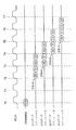
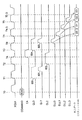
図2は、レイテンシーを種々の値に設定した場合におけるメモリ動作時の図1のデバイスのタイミング図を示す。図2において、CLKは図1のメモリデバイス100の制御ライン118の1つに加えられる外部クロック信号を表す。一実施例において、メモリデバイス100は、66メガヘルツ(66MHZ)乃至300メガヘルツ(300MHZ)の周波数レンジを有するCLK信号で動作できる。COMMANDは、読み出し動作のようなある特定のメモリ動作を実行するためにメモリデバイス100に加えられる命令を表す。OUTPUT DATA210 0−3は、図1のライン114 0−Lの1つに与えられる出力データを表す。各出力データOUTPUT DATA210 0−3は、種々のレイテンシー設定値における出力データを表す。レイテンシー設定値は、図1のモードレジスタ119をプログラムすることにより設定される。レイテンシー設定値が異なると、読み出し命令が出された後、データライン114 0−Nの1つに第1のデータビットが得られるタイミングが異なるものとなる。例えば、レイテンシーが2に設定されると、読み出し命令READの2クロックサイクル後に第1のデータビットD1が得られる。図2において、読み出し命令READが時間T0に発生すると、OUTPUT DATA210−0の第1のデータビットD1は時間T2で得られるが、これは読み出し命令の2クロックサイクル後である。同様に、OUTPUT DATA210 1−3は、レイテンシーの設定が3、4または5であれば、第1のデータビットはT3、T4またはT5で得られるが、これらはそれぞれ読み出し命令の3、4または5クロックサイクル後であることを示す。レイテンシーの設定は、メモリデバイス100の外部の変数に応じて選択される。
FIG. 2 shows a timing diagram of the device of FIG. 1 during memory operation when the latency is set to various values. In FIG. 2, CLK represents an external clock signal applied to one of the
図1のメモリデバイス100は、読み出し動作の各読み出しバーストで4ビットのデータ列を出力できる。読み出し動作において、メモリコントローラ116は、RAS*、CAS*及びWE*のようなある特定の組み合わせの命令信号についてチェックする。その組み合わせが読み出し動作にとって有効であれば、読み出し命令が発せられる。例えば、図2において、読み出し動作のための組み合わせが有効になった後、時間T0において、読み出し命令が発せられる。主メモリ102(図1)の4つのデータビットを読み出して、出力回路112 0−Nの1つへ出力する。主メモリ102の4つのデータビットの読み出しは、従来の任意の読み出し方法で行うことが可能である。出力回路112 0−Nの1つに4ビットのデータが読み出されると、これらのビットはデータライン114 0−Nの1つへシリアルに出力される。ライン114 0−Nに出力される4ビットのデータのタイミングは、レイテンシーの設定に基づき出力コントローラ117により制御される。図2に示すように、各OUTPUT DATA210 0−3の4ビットのデータD0−D3は、異なるレイテンシー設定に応じて、読み出し命令後の異なるクロックサイクル時に出力される。出力回路112 0−N及び出力コントローラ117並びにそれらの動作については、後続の図面を参照して詳述する。
The
図3は、図1の出力回路112 0−Nの1つのブロック図である。図3は出力回路112−0を示す。他の出力回路の構成は図3に示す出力回路112−0の構成と同一である。出力回路112−0は複数の出力パス310 0−3を有する。出力セレクト350は、ラインまたはノード342 0−3を介して出力パス310 0−3に接続されている。出力段360は、ライン356を介して出力セレクト350に接続されている。出力段360は、ライン114−0に接続されて複数のデータビットD0−DNを与える。
FIG. 3 is a block diagram of one of the output circuits 1120-N of FIG. FIG. 3 shows the output circuit 112-0. The configuration of the other output circuits is the same as that of the output circuit 112-0 shown in FIG. The output circuit 112-0 has a plurality of output paths 3100-3. The output select 350 is connected to the output path 3100-3 via lines or nodes 342 0-3.
出力パス310 0−3は、複数の入力セレクト320 0−3を有する。複数の第1のラッチ330 0−3は、ライン322 0−3を介して入力セレクト320 0−3に接続されている。複数の第2のラッチ340 0−3は、ライン332 0−3を介して第1のラッチ330 0−3に接続され、ライン342 0−3を介して出力セレクト350に接続されている。出力パス310 0−3の構成は同一であるため、各出力パス310 0−3は同一構成要素より成る。例えば、出力パス310−0の入力セレクト320−0は、ライン322−0を介して第1のラッチ330−0に接続されている。第2のラッチ34 0−0は、ライン332−0を介して第1のラッチ330−0に接続され、ライン342−0を介して出力セレクト350に接続されている。他の出力パス310 1−3は出力パス310−0と同じ構成である。 The output path 3100-3 has a plurality of input selections 320-0-3. The plurality of first latches 330 0-3 are connected to the input select 320 0-3 via lines 322 0-3. The plurality of second latches 340 0-3 are connected to the first latches 330 0-3 via lines 332 0-3, and are connected to the output select 350 via lines 342 0-3. Since the configurations of the output paths 3100-3 are the same, each output path 3100-3 comprises the same components. For example, the input select 320-0 of the output path 310-0 is connected to the first latch 330-0 via the line 322-0. The second latch 340-0 is connected to the first latch 330-0 via the line 332-0 and is connected to the output select 350 via the line 342-0. The other output paths 310 1-3 have the same configuration as the output path 310-0.
各入力セレクト320 0−3は、複数の入力ノード326に接続されて複数のデータ信号またはデータビットD0−D3を受ける。これらのデータビットは補数データである。別の表現をすると、これらのデータビットはそれぞれ主メモリ102からの真のデータビットとは反対である。データビットD0−D3は、パラレルでノード326において受ける。換言すれば、データビットD0−D3は主メモリ102からノード326に同時に到達する。各入力セレクト320 0−3も、複数のセレクトライン328に接続されて複数のセレクト信号CA0−CA3を受ける。第1のラッチ330 0−3はそれぞれ制御ライン334に接続されている。第2のラッチ340 0−3はそれぞれ制御ライン344に接続されている。制御ライン334、344は複数の伝播制御信号Q0−Q2を受ける。全ての制御ライン334は信号Q2を受ける。第2のラッチ340 0−1の制御ライン344は信号Q0を受ける。第2のラッチ340 2−3の制御ライン344は信号Q1を受ける。
Each input select 320-3 is connected to a plurality of
出力セレクト350は、複数のマルチプレクサ352 0−3を有する。各マルチプレクサ352 0−3の入力はノード342 0−3の1つに接続され、出力はライン356を介して出力段360に接続されている。マルチプレクサ352 0−3はまた、複数の制御ライン354に接続されて複数のタイミング信号DLL 0−3を受ける。
The output select 350 includes a plurality of multiplexers 352 0-3. The input of each multiplexer 352 0-3 is connected to one of nodes 342 0-3, and the output is connected to
図3において、各入力セレクト320 0−3は、ライン326上の4つのデータビットD0−D3のうち1つを選択し、選択したビットを対応するライン322 0−3のうちの1つへ送る。データビットD0−D3の間の1つのデータビットの選択は、ライン110 0−X(図1)上で受ける2つのアドレス信号またはアドレスビットに基づく。ライン110−X上で受けるアドレスビットはA0、A1、A3、…、AXである。ビットA1及びA0の論理値(論理1または0)は、入力セレクト320 0−3によるデータビットの選択を決定する。A1及びA0の論理値が0と0(二進00)であれば、入力セレクト320 0−3によるデータビットの選択はそれぞれD0、D1、D2、D3である。換言すれば、A1A0の組み合わせが00であれば入力セレクト320−0はビットD0を選択し、入力セレクト320−1はビットD1を選択し、入力セレクト320−2はビットD2を選択し、入力セレクト320−3はビットD3を選択する。A1A0の組み合わせが01であれば、入力セレクト320 0−3により選択されるデータの順序はそれぞれD1、D2、D3、D0である。A1A0の組み合わせが10であれば、入力セレクト320 0−3により選択されるデータの順序はD2、D3、D0、D1である。A1A0の組み合わせが11であれば、入力セレクト320 0−3により選択されるデータの順序はD3、D0、D1、D2である。例えば、A1A0の組み合わせが00であれば、図3において、入力セレクト320 0−3により選択されてライン322 0−3へ送られる4つの異なるデータビットはそれぞれD0、D1、D2、D3である。
In FIG. 3, each input select 320 0-3 selects one of the four data bits D0-D3 on
ラッチ330 0−3及び340 0−3は、信号QL0−QL2により制御される。ラッチ330 0−3又は340 0−3は、信号QL0−QL2が作動されるとデータ信号またはデータビットを1つのノードから別のノードへ通過させる。QL2が作動されると、即ち、低い信号レベル(LOW)から高い信号レベル(HIGH)へ変化すると、第1のラッチ330 0−3はデータをノード322 0−3からノード332 0−3へ送る。QL0が作動されると、第2のラッチ340 0−1はデータをノード332 0−1からノード342 0−1へ送る。QL1が作動されると、第2のラッチ340 2−3はデータをノード332 2−3からノード342 2−3へ送る。上記の例では、QL0−QL3が作動された後、データビットD0−D3はライン322 0−3からノード332 0−3へ送られ、最後にノード342 0−3へ送られる。 Latches 330 0-3 and 340 0-3 are controlled by signals QL0-QL2. Latches 330 0-3 or 340 0-3 pass data signals or data bits from one node to another when signals QL0-QL2 are activated. When QL2 is activated, i.e., changes from a low signal level (LOW) to a high signal level (HIGH), the first latch 330 0-3 sends data from node 322 0-3 to node 332 0-3. . When QL0 is activated, the second latch 340 0-1 sends data from node 332 0-1 to node 342 0-1. When QL1 is activated, the second latch 340 2-3 sends data from node 332 2-3 to node 342 2-3. In the above example, after QL0-QL3 is activated, data bits D0-D3 are sent from lines 322 0-3 to nodes 332 0-3 and finally to nodes 342 0-3.
出力セレクト350は、ノード342 0−3上のデータビットを選択してそれらを出力段360へ順次供給する。タイミング信号DLL0−DLL3は、順次作動されてノード342 0−3上のデータビットをライン356を介して出力段360へ送る。かくして、出力セレクト350はデータビットをシリアルに出力段360へ送る。出力段360へ送られるシリアルなデータビットのうち第1のデータビットは、出力パス310−0のライン342−0上のデータビットである。出力段360へ送られる第2のデータビットは、出力パス310−2からのライン342−1のデータビットである。このパターンで、出力段360へ送られる第3及び第4のデータビットは、ライン342−2及び342−3からのものである。上記の例では、出力段360へ送られる第1のデータビットはD0である。出力段360へ送られる第2、第3及び第4のデータビットはD1、D2、D3である。
Output select 350 selects the data bits on nodes 3420-3 and supplies them sequentially to
出力段360は、ライン356上のデータビットを受けてそれらをライン114−0へシリアルに出力する。上記と同じ例を用いると、ライン114−0上に出力されるデータビットはD0、D1、D2、D3である。出力段360は、出力ライン114−0上のデータビットD0−D3を真の形で出力する。換言すれば、ライン114−0上に出力されるデータはライン326上のデータとは反対の電位を有する。この説明の例に用いるデータビットの順序はD0、D1、D2、D3である。しかしながら、データビットの順序は上述したアドレスビットA1、A0の論理値に応じた任意の順序でよい。例えば、ライン342 0−3上のデータがそれぞれD1、D2、D3、D0であれば、データビットは同じ順序で出力段360へ送られる。この場合、出力段360は同じ順序で、即ち、D1、D2、D3、D0の順序でデータビットをライン114−0へ出力する。要約すると、A1A0のアドレスビットの組み合わせが00であれば、ライン114−0におけるデータビットの出力順序はD0、D1、D2、D3であり、A1A0が01であれば、出力データはD1、D2、D3、D0であり、A1A0が10であれば、出力データはD2、D3、D0、D1、さらにA1A0が11であれば、出力データはD3、D0、D1、D2である。
図4は、レイテンシーを2に設定した図3の出力回路112−0の動作を示すタイミング図である。図4において、CA信号はライン328上で受けるCA0−CA3信号の1つを表す。QL0、QL1、QL2信号は、図3の第1及び第2のラッチ330、340で受けるのと同じ信号を表す。DLL0、DLL1、DLL2、DLL3は、出力セレクト350のライン354上で受けるのと同じ信号を表す。出力データD0、D1、D2、D3は、ライン114−0上の出力データD0−D3を表す。
FIG. 4 is a timing chart showing the operation of the output circuit 112-0 of FIG. In FIG. 4, the CA signal represents one of the CA0-CA3 signals received on
図4を参照して、図3のデバイスの動作を説明する。図4において、時間T0でREAD命令が発せられる。メモリセル102(図1)の4つのデータビットにアクセスする。4つのデータビットは、図3の出力回路112−0のデータパス310 0−3へ順次転送される。データパス310 0−3の入力セレクト320 0−3は、ライン326上において4つのデータビットD0−D3を受ける。ライン326において、4つのデータビットはそれらの補数の形で表わされている。図4の時間TAにおいて、信号CAがHIGHに切換ると、各入力セレクト320 0−3はライン326上の4つのビットD0−D3の中から1つのデータビットを選択することができる。選択されたデータビットはライン322 0−3へ送られる。本発明を説明する目的で、A1A0は00であると仮定する。従って、ライン322 0−3へ送られる4つのデータビットはそれぞれD0、D1、D2、D3である。換言すれば、ライン322−0はデータビットD0を運び、ライン322−1はデータビットD1を、ライン322−2はデータビットD2を、またライン322−3はデータビットD3を運ぶ。
The operation of the device of FIG. 3 will be described with reference to FIG. In FIG. 4, a READ command is issued at time T0. Access the four data bits of memory cell 102 (FIG. 1). The four data bits are sequentially transferred to the data path 3100-3 of the output circuit 112-0 in FIG. Input select 320 0-3 of data path 3100-3 receives four data bits D0-D3 on
レイテンシーが2では、信号QL2は常にHIGHである。図4に示すように、QL2信号はREAD命令の開始時から全てのクロックサイクルについてHIGHである。QL2がHIGHであれば、ライン322 0−3上のD0−D3はラッチ330 0−3を通ってノード332 0−3へ送られる。時間TAにおいて、QL0信号はHIGHに切換わる。これにより、データビットD0及びD1はノード332 0−1から第2のラッチ340 0−1を介してノード342 0−1へ通過することができる。時間TBにおいて、QL1はHIGHに切換わる。これにより、データビットD2及びD3はノード322 2−3から第2のラッチ340 2−3を通って342 2−3へ通過することができる。 When the latency is 2, the signal QL2 is always HIGH. As shown in FIG. 4, the QL2 signal is HIGH for all clock cycles from the start of the READ instruction. If QL2 is HIGH, D0-D3 on lines 322 0-3 are sent to nodes 332 0-3 through latches 330 0-3. At time TA, the QL0 signal switches to HIGH. This allows data bits D0 and D1 to pass from node 332 0-1 to node 342 0-1 via second latch 340 0-1. At time TB, QL1 switches to HIGH. This allows data bits D2 and D3 to pass from node 322 2-3 through second latch 340 2-3 to 342 2-3.
出力セレクト350では、マルチプレクサ352 0−3がタイミング信号DLL0−DLL3により制御される。DLL0−DLL3信号は、ノード342 0−3上のビットD0−D3がレイテンシーの設定に応じてライン114−0へ適正に出力できるように順次作動される。レイテンシーの設定が2であるため、ライン114−0上に出力される第1のデータビットはREAD命令の2クロックサイクル後に現れる。この場合、第1のデータビットは時間T2に現れる。ノード342−0上の第1のビットを通過させるには、DLL0信号を作動させる。これにより、データビットD0はノード342−0からノード356へ、そしてライン114−0へ通過することができる。ノード342−0からノード114−0へ伝播遅延が存在するため、データビットD0がライン114−0に現れる時、時間T2においてそれがクロック信号CLKの上昇エッジに一致するように、信号DLL0は時間T2の直前に作動される。図4において、DLL0は時間T2の前に作動され、HIGHに切換わる。これにより、時間T2でデータビットD0(真)はCLK信号の上昇エッジに並ぶことができる。同様に、DLL2は時間T3の前にHIGHに作動されるため、データビットD2は時間T2においてCLK信号の上昇エッジに並ぶことができる。同様に、信号DLL1及びDLL3はそれぞれ時間T2.5及びT3.5の前にHIGHに作動されるため、データビットD1及びD3は時間T2.5及びT3.5においてCLK信号の下降エッジに並ぶことができる。
In the output select 350, the multiplexers 352 0-3 are controlled by the timing signals DLL0-DLL3. The DLL0-DLL3 signals are activated sequentially so that bits D0-D3 on nodes 3420-3 can be properly output on line 114-0 depending on the latency setting. Since the latency setting is 2, the first data bit output on line 114-0 appears two clock cycles after the READ instruction. In this case, the first data bit appears at time T2. To pass the first bit on node 342-0, the DLL0 signal is activated. This allows data bit D0 to pass from node 342-0 to
図5は、レイテンシーの設定が3である図3の出力回路112−0の動作を示すタイミング図である。レイテンシーが3であれば、出力データの第1のビットはREAD命令が発せられた3クロックサイクル後にライン114−0上に現れる。図5において、D0は時間T3に現れるが、これは時間T0のREAD命令の3クロックサイクル後である。レイテンシーが3では、ライン326上のデータビットD0−D3はレイテンシー2の場合と同様にライン114Aへ出力される。レイテンシー2と3の相違点は、信号CA、QL0、QL1及びDLL0−DLL3のタイミングにある。レイテンシー3の出力データはレイテンシー2の出力データより1クロックサイクル遅れてライン114−0に現れるため、信号CAはほとんど1クロックサイクル後に作動される。図5において、CA信号は、図4の時間TAのほとんど1クロックサイクル後である時間TAにおいてHIGHに作動される。QL2は、レイテンシー2の場合と同様に、読み出しサイクルの間中HIGHを維持する。しかしながら、他の信号は、図5に示すようにほとんど1クロックサイクル後に作動される。
FIG. 5 is a timing chart showing the operation of the output circuit 112-0 of FIG. If the latency is 3, the first bit of output data appears on line 114-0 three clock cycles after the READ instruction is issued. In FIG. 5, D0 appears at time T3, which is three clock cycles after the READ instruction at time T0. When the latency is 3, the data bits D0 to D3 on the
図6は、レイテンシーの設定が4である図3の出力回路112−0の動作を示すタイミング図である。レイテンシー設定が4だと、出力データの第1のビットはREAD命令が発せられた4クロックサイクル後にライン114−0上に現れる。図6において、D0は時間T0のREAD命令から4クロックサイクル後の時間T4に現れる。レイテンシー4では、ライン326上に受けるデータビットD0−D3はレイテンシー2と同様にライン114−0へ出力される。しかしながら、4ビット1つの群の最後のビット及び4ビットの次の群の最初のビットを適正に出力できるようにするため異なるタイミング方式が提供される。従って、QL2信号は、レイテンシー2及び3の場合と同様に常にHIGHというわけではない。
FIG. 6 is a timing chart showing the operation of the output circuit 112-0 of FIG. If the latency setting is 4, the first bit of output data appears on line 114-0 four clock cycles after the READ instruction is issued. In FIG. 6, D0 appears at time T4, four clock cycles after the READ instruction at time T0. In
図6において、QL0及びQL1の点線部分は前の読み出しサイクルからの信号を示す。600及び601において点線で示す信号は、QL0及びQL1信号の前の変化を示す。604及び605における信号は、現在の読み出しサイクルにおけるQL0及びQL1の現在の変化である。602における信号はQL2信号の現在の変化である。図3において、現在の読み出しサイクルの現在のビットD0−D3が前の読み出しサイクルの前のビットD0−D3と混同されないようにするため、ノード332 0−3上の前のビットD0−D3を現在のビットD0−D3がノード332 0−3に到達する前にノード342 0−3へ送る必要がある。従って、QL2は、QL0信号の変化とQL1信号の変化との間で作動させなければならない。換言すれば、QL2は、前の読み出しサイクルのQL0の変化の後で現在の読み出しサイクルのQL0の変化の前に作動する必要がある。 In FIG. 6, the dotted line portions of QL0 and QL1 indicate signals from the previous read cycle. Signals indicated by dotted lines at 600 and 601 indicate previous changes in the QL0 and QL1 signals. The signals at 604 and 605 are the current changes in QL0 and QL1 in the current read cycle. The signal at 602 is the current change in the QL2 signal. In FIG. 3, to prevent the current bits D0-D3 of the current read cycle from being confused with the bits D0-D3 prior to the previous read cycle, the previous bits D0-D3 on nodes 332 0-3 are now Bits D0-D3 need to be sent to nodes 342 0-3 before reaching nodes 332 0-3. Therefore, QL2 must be operated between the change of the QL0 signal and the change of the QL1 signal. In other words, QL2 needs to operate after the change of QL0 of the previous read cycle and before the change of QL0 of the current read cycle.
図6に示すように、QL2は602において変化するが、これは、600におけるQL0の変化の後で604におけるQL0の変化の前である。同様に、602におけるQL2の変化も、601におけるQL1の変化の後で605におけるQL1の変化の前である。従って、QL2が602において変化すると、ライン322 0−3上の現在のビットD0−D3はノード332 0−3へ送られる。この時(602)までに、前のビットD0−D3は、600及び601におけるQL0及びQL1の変化により既にノード342 0−3へ送られている。従って、レイテンシー4において信号QL0−QL3を適正に作動することにより、出力回路112−0は全ての読み出しサイクルにおいてビットD0−D3を正しく処理する。
As shown in FIG. 6, QL2 changes at 602, which is after the change of QL0 at 600 and before the change of QL0 at 604. Similarly, the change in QL2 at 602 is also after the change in QL1 at 601 and before the change in QL1 at 605. Thus, when QL2 changes at 602, the current bits D0-D3 on lines 322 0-3 are sent to nodes 332 0-3. By this time (602), the previous bits D0-D3 have already been sent to nodes 3420-3 due to changes in QL0 and QL1 at 600 and 601. Thus, by properly operating signals QL0-QL3 at
図7は、レイテンシーの設定が5である図3の出力回路112−0の動作を示すタイミング図である。レイテンシーが5では、出力データの最初のビットはREAD命令が発せられた5クロックサイクル後にライン114−0上に現れる。図7において、D0は、時間T0でのREAD命令から5クロックサイクル後の時間T5で現れる。レイテンシー5では、326上で受けるデータビットD0−D3は、レイテンシー2の場合と同様にライン114−0へ出力される。レイテンシーが5である場合の出力パス112−0の動作タイミングは、レイテンシー4の時のタイミングと同じである。図6と同様に、図7の点線で示す信号は前の読み出しサイクルからの信号である。図7において、信号QL2は702において作動またはHIGHに変化する。この変化は、704及び705におけるQL0及びQL1の変化の前であって、700及び701におけるQL0及びQL1の変化の後である。この時(702)までに、前のビットD0−D3は、700及び701におけるQL0及びQL1の変化により既にノード342 0−3へ送られている。従って、レイテンシー5では、信号QL0−QL3を適正に作動することにより、出力回路112−0は全ての読み出しサイクルにおいてビットD0−D3を正しく処理する。
FIG. 7 is a timing chart showing the operation of the output circuit 112-0 of FIG. With a latency of 5, the first bit of output data appears on line 114-0 five clock cycles after the READ instruction is issued. In FIG. 7, D0 appears at time T5, five clock cycles after the READ instruction at time T0. In
図8A−Dは、図3の入力セレクト320 0−3の概略図である。図8A−Dの各入力セレクト320 0−3は、複数のマルチプレクサ810 0−3を有する。簡略を期するために、異なる入力セレクト320 0−3間のマルチプレクサの参照番号は同じである。図8Aにおいて、各マルチプレクサ810 0−3の入力は、データD0−D3のビットの1つを受ける対応の入力ライン326のうちの1つに接続されている。マルチプレクサ810 0−3はまた、ノード812に接続された複数の出力を有する。記憶素子814は、第1の記憶ノードがノード812においてマルチプレクサ810 0−3の出力に接続され、第2の記憶ノードがノード322 0−3の1つに接続されている。各マルチプレクサ810 0−3は、ライン328上で受信される信号CA0−CA3の1つにより制御される。
8A-D are schematic diagrams of the input select 3200-3 of FIG. Each input select 320 0-3 in FIGS. 8A-D has a plurality of multiplexers 810 0-3. For the sake of brevity, the reference numbers of the multiplexers between the different input selects 320-3 are the same. In FIG. 8A, the input of each multiplexer 810 0-3 is connected to one of the
図8B−Dにおいて、入力セレクト310 1−3は図8Aの入力セレクト310−0と同じ構成である。しかしながら、入力セレクト310 1−3の入力326はデータビットD0−D3を異なる順序で受ける。図8Aにおいて、入力326−0、326−1、326−2、326−3はそれぞれD0、D1、D2、D3をこの順序で受ける。図8Bにおいて、入力326−0、326−1、326−2、326−3において受信されるD0−D3の順序はそれぞれD1、D2、D3、D0である。図8Cにおいて、入力326−0、326−1、326−2、326−3により受信される信号D0−D3の順序はD2、D3、D0、D1である。図8Dにおいて、入力326−0、326−1、326−2、326−3において受信されるD0−D3の順序はそれぞれD3、D0、D1、D2である。
8B-D, the input select 3101-3 has the same configuration as the input select 310-0 of FIG. 8A. However,
図8A−Dの入力セレクト320 0−3の動作は同じである。CA 0−3信号の1つが作動されると、その作動されたCA信号により制御される対応のマルチプレクサは、ビットD0−D3の1つをノード326の1つからノード812へ、そしてノード322 0−3の1つへ送る。例えば、図8Aにおいて、CA0が作動またはHIGHに変化すると、マルチプレクサ810−0はノード326からノード812へ、そしてノード322−0へビットD0を送る。CA1が作動されると、ビットD1がノード322−0へ送られる。同様に、CA2またはCA3が作動されると、ビットD2またはD3がノード322−0へ送られる。
The operation of the input select 320-3 in FIGS. 8A-D is the same. When one of the CA 0-3 signals is activated, the corresponding multiplexer controlled by the activated CA signal moves one of bits D0-D3 from one of
信号CA 0−3のただ1つが一度に作動される。信号CA 0−3の作動の順序は、アドレスビットA1及びA0の論理値に基づく。A1A0が00であれば、CA0が作動され、A1A0が01であれば、CA1が作動され、A1A0が10であれば、CA2が作動され、そしてA1A0が11であれば、CA3が作動される。これらの順序は、図3のデータビットD0−D3が選択される順序と一致している。例えば、A1A0が10であれば、CA2が作動される。図8Aにおいて、信号CAにより制御されるマルチプレクサ810−2はD2をノード322−0へ送る。データビットD2はそのシリアルデータの第1のビットである。図8Bにおいて、信号CA2により制御されるマルチプレクサ81 0−2はD3をノード322−1へ送る。ビットD3はそのシリアルデータの第2のビットである。同様に、図8C及び8Dのマルチプレクサ810−2はそれぞれビットD0及びD1をノード322−2及び322−3へ送る。従って、A1A0が10であれば、信号CA2が作動され、これにより入力セレクト320 0−3がビットD2、D3、D1及びD0を選択する。これは、図3の入力セレクト320 0−3の選択とマッチする。 Only one of the signals CA 0-3 is activated at a time. The order of operation of signals CA 0-3 is based on the logical values of address bits A1 and A0. If A1A0 is 00, CA0 is activated, if A1A0 is 01, CA1 is activated, if A1A0 is 10, CA2 is activated, and if A1A0 is 11, CA3 is activated. These orders match the order in which data bits D0-D3 in FIG. 3 are selected. For example, if A1A0 is 10, CA2 is activated. In FIG. 8A, multiplexer 810-2 controlled by signal CA sends D2 to node 322-0. Data bit D2 is the first bit of the serial data. In FIG. 8B, multiplexer 810-2 controlled by signal CA2 sends D3 to node 322-1. Bit D3 is the second bit of the serial data. Similarly, multiplexers 810-2 of FIGS. 8C and 8D send bits D0 and D1 to nodes 322-2 and 322-3, respectively. Thus, if A1A0 is 10, the signal CA2 is activated, causing the input select 320-0-3 to select bits D2, D3, D1, and D0. This matches the selection of input select 3200-3 in FIG.
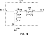
図9は、図3の出力パス310−0の第1のラッチ330−0を示す概略図である。ラッチ330−0は、ライン916により記憶素子914に接続されたマルチプレクサ912を有する。マルチプレクサ912は、入力Dがノード322−0に接続され、出力がノード916に接続されている。マルチプレクサ912は、そのクロックまたはCLK端子がライン334に接続されてQL2信号を受ける。マルチプレクサ912はまたライン915に接続されるが、このラインはインバータ917の出力に接続されている。インバータ917は、ライン334上のQL2信号を受け、ライン915上に補数信号QL2*を発生する。記憶素子914は、第1の記憶ノードQがノード916に接続され、第2の記憶ノードQ*がライン332−0に接続されている。図9は出力パス310−0の第1のラッチ330−0だけを示すが、他の出力パス310 1−3の第1のラッチ330 1−3及び第2のラッチ340 0−3は図9のラッチ330−0と同じである。従って、図3の他の第1及び第2のラッチの動作は図9のラッチ330−0の動作と同じである。
FIG. 9 is a schematic diagram illustrating the first latch 330-0 of the output path 310-0 of FIG. Latch 330-0 has a
図9を参照して、信号QL2が作動されない場合、マルチプレクサ912は閉じており、ライン322上のデータまたは信号がマルチプレクサ912を通過するのを阻止する。信号QL2が作動されると、マルチプレクサ912が開いて、ライン322−0上のデータまたは信号がマルチプレクサを介してライン916及び332−0に送られるようにする。信号は、1つの信号レベルから別の信号レベルへ変化すると、作動される。この場合、信号QL2は、低い信号レベル(LOW)から高い信号レベル(HIGH)へ変化すると作動される。従って、図9において、QL2がLOWからHIGHへ切換わると、ライン322−0上のデータがライン322−0へ送られる。同様に、図3では、QL0及びQL1が作動されると、ライン332 0−3上のデータがラッチ340 0−3を介してライン342 0−3へ送られる。
Referring to FIG. 9, when
図10は、図3の出力段360の概略図である。出力段360は、ノード356に接続されて出力セレクト356からデータビットD0−D3を受ける記憶素子1002を有する。記憶素子1002はまた、ノード1008においてNORゲート1004の第1の入力とNANDゲート1006の第1の入力に接続されている。NORゲート1004の第2の入力は、ノード1010において記憶素子1014に接続されている。NANDゲートの第2の入力は、ノード1012において記憶素子1014に接続されている。NORゲート1004の出力は、インバータ1016を介してpチャンネルトランジスタ1020のゲートに接続されている。NAND1006の出力は、インバータ1018を介してnチャンネルトランジスタ1022のゲートに接続されている。トランジスタ1020のソースは電源に接続され、ドレインはデータパッド114−0に接続されている。トランジスター1022のドレインはアースに接続され、ソースはデータパッド114に接続されている。信号DLL0がノード1026に与えられるが、このノードはマルチプレクサ1024に接続されている。マルチプレクサ1024は、信号QEDを受けるために入力がノード1028に接続され、出力がノード1010に接続されている。
FIG. 10 is a schematic diagram of the
動作について説明すると、記憶素子1002は、シリアルなデータビットD0−D3を受けて、それらのビットをNORゲート1004とNANDゲート1006の第1の入力であるノード1008へ送る。ある特定の時間、例えば、図4に示す時間TBにおいて、DLL0はHIGHに変化する。これにより、マルチプレクサ1024は信号QEDをノード1010及び1012に送る。NORゲート1004及びNANDゲート1006はノード1010及び1012におけるQED信号とノード1008における信号との組み合わせに基づきトランジスタ1020またはトランジスタ1022の何れかをオンにする。トランジスタ1020がオンになると、ノード114−0が電源(HIGH)に引き寄せられる。トランジスタ1022がオンになると、ノード114−0がアース(LOW)へ引き寄せられる。ノード114−0におけるHIGHまたはLOWはデータD0−D3の1つを表すが、これはライン316から受ける対応の補数データビットD0−D3の1つとは反対である。
In operation,
図11は、図1の出力コントローラ117のブロック図である。出力コントローラ117は、ライン1112−1115上の複数のレイテンシー信号LATE2−LATE5と、ライン1116上の読み出し信号RDWと、ライン1118上の遅延ロックループクロック信号CLKDQを受けるレイテンシー入力回路1110を備えている。レイテンシー入力回路1110は、ライン1120−1123において複数の出力を有し、複数の信号QED、QSP2、QSP3、QSP1*を与える。出力タイミングイネーブル回路1130は、ライン1118及び1123を介してレイテンシー入力回路1110に接続され、CLKDQ及びQSP1*信号を受ける。出力タイミングイネーブル回路1130は、ライン1132上に第1のイネーブル信号CLKLを、またライン1334上に第2のイネーブルCLKHを発生する。出力タイミング発生器1150は、ライン1132及び1134を介して出力タイミングイネーブル回路1130に接続され、信号CLKL及びCLKHを受ける。信号CLKL及びCLKHにより、出力タイミング発生器1150はライン1552−1155上にタイミング信号DLL0−DLL3を発生することができる。DLL0−DLL3信号は、図3において説明したように出力セレクト350を制御するために使用される。伝播制御信号発生器1170は、ライン1121−1123を介してレイテンシー入力回路1110に接続され、またライン1152−1155を介して出力タイミング回路1150に接続されて、QSP2、QSP3、QSP1*及びDLL0−DLL3信号を受ける。伝播制御信号発生器1170は、ライン1172−1174上にQL0−QL2信号を発生する。QL0−QL2信号は、図3の第1及び第2のラッチ330 0−3及び340 0−3を作動するために使用する。
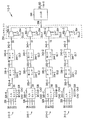
FIG. 11 is a block diagram of the
以下の説明において、「フリップフロップ」は当業者によって広く理解されている常用の回路コンポーネントを指す。以下の説明におけるフリップフロップは、正のエッジでトリガーされるフリップフロップである。しかしながら、本発明の説明を読むと、当業者は、負のエッジでトリガーされるフリップフロップまたは他のタイプの同様なコンポーネントにより同じ結果が得られる。さらに、以下の説明において、「ラッチ」または「パススルーラッチ」は普通の回路コンポーネントの意味である。ラッチは入力から出力へデータ又は信号を通過させるために使用する。以下の説明で言及するラッチは、図9のラッチ33 0−0と同じものでよい。 In the following description, “flip-flop” refers to conventional circuit components that are widely understood by those skilled in the art. The flip-flop in the following description is a flip-flop triggered on a positive edge. However, upon reading the description of the present invention, those skilled in the art will achieve the same result with flip-flops or other types of similar components triggered by negative edges. Further, in the following description, “latch” or “pass-through latch” means ordinary circuit components. A latch is used to pass data or signals from input to output. The latch referred to in the following description may be the same as the latch 330-0 of FIG. 9.
図12は、図11のレイテンシー入力回路1110の概略図である。レイテンシー入力回路1110は、パススルーラッチ(LAT)1210と、複数のフリップフロップ(FF)1212−1214とを有する。ラッチ1210及びフリップフロップ1212−1214は、ライン1118上においてCLKDQを受ける。ラッチ1210及びFF1212は、ライン1116上において信号RDWを受ける。複数のマルチプレクサ1216−1219は、ライン1212−1115上でLATE2−LATE5を受けてRDW信号をノード1230へ通過させる。フリップフロップ1232は、入力がインバータ1235を介してノード1230に接続されている。フリップフロップ1232の出力は、ノード1123においてラッチ1234の入力に接続されて、信号QSP1*を与える。ラッチ1234の出力は、ノード1122においてラッチ1236の入力に接続され、信号QSP2を与える。ノード1122はまた、直列接続のインバータ1242、1244を介してQED信号を与える。ラッチ1236の出力は、インバータ1240を介してノード1121に接続され、信号QSP3を与える。フリップフロップ1232、1234及び1236のクロック入力もCLKDQを受ける。
FIG. 12 is a schematic diagram of the
RDWは、入力信号CS*、RAS*及びWE*の組み合わせが有効である時メモリコントロール116により発生される信号である。LATE2−LATE5信号も、メモリデバイス100にプログラムされたレイテンシーに基づき制御回路116により発生される。CLKDQ信号は、メモリデバイス100の遅延ロックループにより与えられる。遅延ロックループは、普通の回路であって、当該技術分野で広く知られた遅延ロックループのうちの1つでよいため図示しない。
RDW is a signal generated by
図12において、信号QSP1*、QSP2及びQSP3は、信号RDWがラッチ1210またはフリップフロップ1212−1214のうちの1つを伝播することにより発生される。レイテンシーの設定が2であれば、RDWはラッチ1216を通過してノード1230へ至る。レイテンシーの設定が3、4または5であれば、RDW信号はフリップフロップ1212−1214のうちの1つ、2つまたは3つへ送られる。信号LATE2−LATE5は、マルチプレクサ1216−1219を介してノード1230へ送られるREW信号への通過を制御する。
In FIG. 12, signals QSP1 *, QSP2 and QSP3 are generated as signal RDW propagates through one of
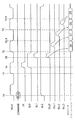
図12のレイテンシー入力回路1110の動作を、図16のタイミング図を参照して説明する。本発明を説明する目的で、メモリデバイス100はレイテンシーが4にプログラムまたは設定されているため、信号LATE4だけが作動されると仮定する。この場合、データパッド114−0では読み出し命令が有効になった4クロックサイクル後に第1のデータビットが生じる。図16において、CLKDQ及びCLK信号は読み出し動作を予想してA及びBにおいてHIGHに変化する。時間T0では、読み出し命令READはCにおいてHIGHに変化し、新しい読み出し動作の開始を示す。Dにおいて、信号RDWはHIGHに切換わる。図12において、信号RDWがフリップフロップ1212及び1213を伝播すると、LATE4信号はマルチプレクサ1218を作動して信号RDWを図12のノード1230へ送る。RDW信号がHIGHであるため、ノード1230のところの信号もHIGHである。図16において、ノード1230はEにおいてHIGHに切換わる。ノード1230がHIGHになると、インバータ1235の出力は強制的にLOWにされる。インバータ1235の出力の信号はまた、フリップフロップ1232の入力信号である。CLKDQはHIGHであるから、フリップフロップ1232はノード1123上のその出力の信号をLOWにするが、これはQSP1*信号を表す。図16において、QSP1*はFにおいてLOWに切換わる。その後、ノード1123の信号はラッチ1234を介してノード1122へ、さらにラッチ1236を介してノード1121へ伝播する。ノード1122における信号を信号QSP2として表し、ノード1121における信号をQSP3として表す。図16において、ノード1123における信号QSP1*がLOWになると、信号QSP2がGにおいてHIGHに切換わり、信号QSP3がHにおいてHIGHに切換わる。さらに、ノード1120における信号QEDはインバータ1242及び1244により信号QSP2に追従する。信号QSP1*、QSP2及びQSP3は他の回路の入力信号として使用する。信号QEDは、図10に示すようにデータを出力するためのストローブ信号として使用する。
The operation of the
図13は、図11の出力タイミングイネーブル回路1130を示す概略図である。出力タイミングイネーブル回路1130は、ライン1123に接続され、信号QSP1*を受けてノード1317にラッチリセット信号LRSTを発生するパルス回路(PULSE)1315を有する。フリップフロップ1320は、リセットRS入力、クロックCLK入力、データ入力D及び相補出力Q及びQ*を有する。RS入力は、LRST信号を受けるためにノード1317に接続されている。CLK入力はノード1312により遅延回路1314に接続され、遅延されたCLKDQ信号を受ける。入力D及び出力Q*は互いに接続されている。出力Qは、インバータ1316及び1318を介してライン1132上に信号CLKLを与える。直列接続のラッチ1322及び1324は、ライン1312上の遅延されたCLKDQ信号を受けて、ライン1134上に信号CLKHを与える。ノード1134は、インバータ1332よりなるフィードバックループを介して入力Dに接続されている。トランジスタ1328のゲートは遅延されたLRST信号を受けるために遅延回路1330に接続されている。トランジスタ1326のソースはアースに接続され、ドレインはラッチ1324のリセットRS端子に接続されている。LRST信号が作動(HIGH)されると、トランジスタ1328はオンになり、ラッチ1324をリセットする。ラッチ1324がリセットされると、ノード1134の信号CLKHがLOWになる。LRST信号はまた、ラッチ1320を同じようにリセットする。LRST信号が作動されてHIGHになると、ノード1132上の信号CLKLが強制的にLOWにされる。
FIG. 13 is a schematic diagram showing the output timing enable
図13において、CLKH及びCLKL信号は信号CLKDQ信号に基づき発生される。イネーブル信号CLKL及びCLKHは、信号DLL0−DLL3を作動するために使用され、これらの信号により読み出し動作時にデータをデータパッド114 0−Nへ転送することができる。データが各読み出し動作時に適正に転送されるようにするため、LRST信号は新しい読み出しコマンドを受ける度に作動される。LRSTは、信号CLKH及びCLKLをリセットしてデータが適正に転送されるようにする。 In FIG. 13, the CLKH and CLKL signals are generated based on the signal CLKDQ signal. Enable signals CLKL and CLKH are used to operate signals DLL0-DLL3, and these signals allow data to be transferred to data pads 1140-N during a read operation. The LRST signal is activated each time a new read command is received to ensure that the data is properly transferred during each read operation. The LRST resets the signals CLKH and CLKL so that the data is properly transferred.
再び図16を参照して、QSP1*がFにおいてLOWに切換わると、RDWがDにおいてHIGHになる新しい読み出し動作の結果、パルス回路がIにおいてパルスLRSTを発生する。信号LRSTが作動されると、J及びKに示すようにCLKH及びCLKL信号がLOWにリセットされる。J及びKにおいてLOWにリセットされた後、CLKH予及びCLKL信号は別のリセットがなされるまでCLKDQ信号だけの影響を受ける。例えば、CLKHはL、M及びNにおいてその通常の変化に戻り、CLKL信号はO、P及びQにおいてその通常の変化に戻る。図16に示すように、CLKH及びCLKLは異なる相を有する。換言すれば、CLKH及びCLKLは同期状態にない。CLKH及びCLKL信号は、図14の出力タイミング発生器1150をイネーブルするために使用する。
Referring again to FIG. 16, when QSP1 * switches to LOW at F, the pulse circuit generates a pulse LRST at I as a result of a new read operation in which RDW goes HIGH at D. When the signal LRST is activated, the CLKH and CLKL signals are reset to LOW, as shown at J and K. After being reset LOW at J and K, the CLKH pre and CLKL signals are only affected by the CLKDQ signal until another reset is made. For example, CLKH returns to its normal change at L, M and N, and the CLKL signal returns to its normal change at O, P and Q. As shown in FIG. 16, CLKH and CLKL have different phases. In other words, CLKH and CLKL are not in a synchronized state. The CLKH and CLKL signals are used to enable the
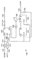
図14は、図11の出力タイミング発生器1150の概略図である。出力タイミング発生器1150は、第1及び第2のタイミング回路1410、1420を有する。両方の回路1410及び1420は同一構成であり、ライン1118において同じCLKDQ信号を受ける。回路1410は、インバータ1411を介してCLKDQの反転信号を受けるパルス発生器1416を有する。パルス発生器1416は、ノード1413において出力信号を発生する。ノード1413の信号は、ライン1153または1155へ送られて信号DLL1またはDLL3となる。ノード1413からライン1153または1155への信号の通過は、マルチプレクサ1415または1418により制御される。マルチプレクサ1415及び1418は、ノード1232におけるCLKLにより制御される。
FIG. 14 is a schematic diagram of the
回路1420は、ノード1429においてその入力にインバータ1411を介してCLKDQを受けるパルス発生器1426を有する。パルス発生器1426はノード1423に出力信号を発生する。ノード1423の信号は、ライン1152または1154へ送られて信号DLL0またはDLL2になる。ノード1423からライン1154または1152への信号の通過は、マルチプレクサ1425または1428により制御される。マルチプレクサ1425及び1428は、ノード1134における信号CLKHにより制御される。
一般的に、パルス発生器1416及び1426は、CLKDQ信号を受けてノード1413及び1423上に出力信号を発生する。ノード1413上の信号は、マルチプレクサ1415または1418を通過して信号DLL1またはDLL3となる。従って、CLKL信号が何れの相にあるかにより、DLL1またはDLL3が発生する。換言すれば、DLL1及びDLL3はCLKL信号の互い違いの相で作動される。同様に、ノード1423上の信号は、マルチプレクサ1425または1428を通過して信号DLL0またはDLL2となる。従って、CLKH信号が何れの相にあるかにより、DLL0またはDLL2の何れかが発生する。換言すれば、DLL0及びDLL2はCLKH信号の互い違いの相で作動される。CLKH及びCLKL信号は同じ相を有さない。このため、それらは、正しい順序のデータビットD0−D3がデータパッド114−0へ出力されるように、DLL0−DLL3を正しく作動することができる。
In general,
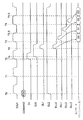
図17は、図14の動作を示すタイミング図である。図17において、ノード1423及び1413の信号は、図14のノード1423及び1413におけるパルス発生器1416及び1426の出力信号を表す。信号CLK、READ、LRST、CKLH及びCKLKは図16の信号と同じである。CLKH信号は、JにおいてLOWになると、マルチプレクサ1428を作動して、ノード1423の信号がインバータ1429を通過できるようにする。この時ノード1423の信号はLOWであるため、インバータ1429の出力信号、即ちDLL0信号はHIGHである。図17において、DLL0はS0においてHIGHに作動される。信号CLKHがLにおいてHIGHになると、マルチプレクサ1425が作動されて、ノード1423の信号がインバータ1427を通過できるようにする。ノード1413の信号はこの時LOWであるため、インバータ1427の出力信号、即ちDLL2信号はHIGHである。図17において、DLL2はS2においてHIGHに作動される。要約すると、CLKHが変化するとタイミング信号DLL0を作動し、CLKHが別の変化をするとタイミング信号DLL2を作動する。例えば、図17において、タイミング信号DLL0及びDLL2は、イネーブル信号CLKHの異なる相の時に作動される。DLL0は信号CLKHが1つの相(CLKHがLOW)の時に作動され、DLL2は信号CLKHが別の相(信号CLKHがHIGH)の時に作動される。換言すれば、タイミングDLL0及びDLL2は、イネーブル信号CLKHの下降エッジ及び上昇エッジの後に作動される。
FIG. 17 is a timing chart showing the operation of FIG. In FIG. 17, the signals at
同様に、CLKL信号がKにおいてLOWになると、マルチプレクサ1418を作動して、ノード1413の信号がインバータ1419へ通過できるようにする。ノード1413の信号はこの時LOWであるため、インバータ1419の出力信号、即ち、DLL1信号はHIGHである。図17において、DLL1はS1においてHIGHに作動される。信号CLKLがOにおいてHIGHになると、マルチプレクサ1415を作動して、ノード1413の信号がインバータ1417へ通過できるようにする。ノード1413の信号はこの時LOWであるため、インバータ1417の出力信号、即ちDLL3信号はHIGHである。図17において、DLL3はS3においてHIGHに作動される。要約すると、CLKLが変化すると、タイミング信号DLL1が作動され、信号CLKLが別の変化をすると、タイミング信号DLL3が作動される。タイミング信号DLL1及びDLL3は、イネーブル信号CLKLの異なる相の時に作動される。例えば、図17において、DLL1は信号CLKLの1つの相(信号CLKLがHIGH)の時に作動され、DLL3は信号CLKLが別の相(信号CLKLがLOW)の時に作動される。換言すれば、信号DLL1及びDLL3は、イネーブル信号CLKLの下降エッジ及び上昇エッジの後に作動される。
Similarly, when the CLKL signal goes LOW at K,
図17において、OUTPUT DATAはデータパッド114−0において出力されるデータビットを示す。レイテンシーが4では、第1のデータビットは時間T4で現れる。本発明を説明する目的で、データパッド114−0におけるデータ出力はD0、D1、D2、D3の転送順序に従うと仮定する。従って、D0及びD2は偶数データビットと呼び、D1及びD3は奇数データビットと呼ぶ。一般的に、データパッド114−0において出力される一連の4つのデータビットでは、偶数データビットは第1及び第3のビットである。奇数データビットは第2及び第4のデータビットである。この場合、偶数データビットD0及びD2は、タイミング信号DLL0及びDLL2がイネーブル信号CLKHの異なる相において作動またはHIGHに変化すると出力される。換言すれば、ビットD0及びD2は、イネーブル信号CLKHの互い違いの相で出力される。同様に、D1及びD3は、タイミング信号DLL1及びDLL3がイネーブル信号CLKLの異なる相で作動されてHIGHになった後出力される。換言すれば、D3はイネーブル信号CLKLの互い違いの相で出力される。 In FIG. 17, OUTPUT DATA indicates a data bit output from the data pad 114-0. With a latency of 4, the first data bit appears at time T4. For purposes of describing the present invention, assume that the data output at data pad 114-0 follows the transfer order of D0, D1, D2, D3. Therefore, D0 and D2 are called even data bits, and D1 and D3 are called odd data bits. In general, in a series of four data bits output at data pad 114-0, the even data bits are the first and third bits. The odd data bits are the second and fourth data bits. In this case, the even data bits D0 and D2 are output when the timing signals DLL0 and DLL2 are activated or changed to HIGH in different phases of the enable signal CLKH. In other words, the bits D0 and D2 are output in alternate phases of the enable signal CLKH. Similarly, D1 and D3 are output after the timing signals DLL1 and DLL3 are activated at different phases of the enable signal CLKL and become HIGH. In other words, D3 is output in alternate phases of the enable signal CLKL.
図15は、図11の伝播制御信号発生器1170の概略図である。伝播制御信号発生器1170は、ノード1155及び1122上でDLL3及びQSP2信号を受けるNORゲート1502を有する。NANDゲート1502の出力はインバータ1504に接続され、このインバータの出力はノード1172に接続されてQL0信号を与える。同様な構成において、NANDゲート1512は、ノード1153及び1121においてDLL1及びQSP3信号を受ける。NANDゲート1512の出力はインバータ1514に接続され、このインバータの出力はノード1173に接続されてQL1信号を与える。伝播制御信号発生器1170はまた、上述した他の回路により発生されるLATE2、LATE3、QED、QSP1*、DLL0及びDLL3のような他の信号も受ける。LATE2及びLATE3信号はNORゲート1532において結合される。DLL0及びDLL2信号はNORゲート1534により結合される。NORゲート1534の出力は、NORゲート1536において信号QED及びQSP1*と結合される。NORゲート1532の出力信号は、マルチプレクサ1544及びトランジスタ1546のゲートを制御する。トランジスタ1546は、作動されると、ノード1174を電源電圧に引き寄せる。マルチプレクサ1544は、作動されると、NORゲート1536の出力信号をノード1174へ通過させる。ノード1174の信号はQL2信号を表す。
FIG. 15 is a schematic diagram of the propagation
図15において、QL0は、DLL3信号及びQSP2信号が共にHIGHになるとHIGHに作動される。同様に、QL1信号は、DLL1信号及びQSP3信号が共にHIGHになった時に限りHIGHに作動される。上述したように、QL2信号は、レイテンシーの設定が2または3であれば常にHIGHに作動されている。図15において、ノード1112または1113のLATE2またはLATE3信号がHIGHであり、レイテンシーの設定が2または3の何れかであることを示す場合、ノード1540におけるNORゲート1532の出力は強制的にLOWとなる。これによりトランジスタ1546がオンになり、ノード1174を電源電圧(HIGH)に接続する。かくして、ノード1174の信号QL2は、LATE2またはLATE3の何れかがHIGHであれば常にHIGHである。LATE2及びLATE3が共にLOWであり、レイテンシーの設定が4または5の何れかがあることを示す場合、ノード1540におけるNORゲート1532の出力は強制的にHIGHになる。これにより、トランジスタ1546はオフになる。かくして、ノード1174の信号QL2は、信号QED、QSP1*、DLL0及びDLL2に依存する。
In FIG. 15, QL0 is activated to HIGH when both the DLL3 signal and the QSP2 signal are HIGH. Similarly, the QL1 signal is activated HIGH only when both the DLL1 signal and the QSP3 signal are HIGH. As described above, the QL2 signal is always operated HIGH when the latency setting is 2 or 3. In FIG. 15, if the LATE2 or LATE3 signal at
図17は、図15の動作のタイミングを示す。図17において、信号QL0−QL2は図15に示すように他の信号と関連で適当な時に作動またはHIGHに変化する。信号QL2の変化は信号QL0の変化の間に起こる。信号QL2の変化も信号QL1の変化の間に起こる。図6及び7を参照して説明したように、QL2信号の変化のタイミングにより、信号QL0及びQL1を適正に作動することができる。これにより、読み出し動作時におけるデータの正確な処理が可能となる。 FIG. 17 shows the timing of the operation of FIG. In FIG. 17, signals QL0-QL2 are activated or changed to HIGH when appropriate in connection with other signals as shown in FIG. The change in signal QL2 occurs during the change in signal QL0. Changes in signal QL2 also occur during changes in signal QL1. As described with reference to FIGS. 6 and 7, the signals QL0 and QL1 can be appropriately operated according to the change timing of the QL2 signal. As a result, accurate processing of data during the read operation is possible.
図18は、本発明によるシステムを示す。この図において、システム1800は、プロセッサ1802がメモリデバイス100に接続されたものである。本発明のメモリデバイス100については、図1を参照して上述した。本発明によると、プロセッサ1802は、制御ライン(CONTROL)を介してメモリデバイス100に制御信号を与える。プロセッサとメモリとの間のデータ通信はデータラインまたはデータバス(DATA)を介して行われ、アドレスはアドレスラインまたはアドレスバス(ADDRESS)を介してメモリへ与えられる。1つの実施例において、プロセッサ1802及びメモリデバイス100は単一のチップ上に作製される。
FIG. 18 shows a system according to the invention. In this figure, a
特定の実施例につき図示説明したが、当業者は、同一目的を達成するように構成された任意の構成を図示説明した特定の構成に置き換え可能なことがわかる。本願は、本発明の任意の変形例及び設計変更を包含するように意図されている。従って、本発明は、頭書の特許請求の範囲及びその均等物によってのみ限定されると意図されている。 Although illustrated and described with respect to particular embodiments, those skilled in the art will recognize that any configuration configured to achieve the same objective may be replaced with the specific configuration illustrated and described. This application is intended to cover any variations and design modifications of the invention. Accordingly, it is intended that the invention be limited only by the appended claims and equivalents thereof.
Claims (13)
出力パスに接続されて、該出力パスからデータビットを受ける出力セレクトと、
出力セレクトから転送されるデータビットを受けて、該データビットをデータパッドへクロック信号の2サイクル以内にシリアルに出力する出力段とより成り、
シリアルな第1及び第3のデータビットは第1のイネーブル信号の互い違いの相で出力され、シリアルの第2及び第4のデータビットは第2のイネーブル信号の互い違いの相で出力され、第1及び第2のイネーブル信号は同期されていない集積回路。A plurality of output paths each receiving in parallel the first, second, third and fourth data bits;
An output select connected to the output path and receiving data bits from the output path;
An output stage for receiving data bits transferred from the output select and serially outputting the data bits to the data pad within two cycles of the clock signal;
The serial first and third data bits are output in staggered phases of the first enable signal, the serial second and fourth data bits are output in staggered phases of the second enable signal, and the first And the second enable signal is not synchronized.
データビットを受ける複数の入力ノードと、
入力ノードに接続されて、データビットから選択された所定のデータビットを発生する入力セレクトと、
入力セレクトに接続されて、選択されたデータビットを受ける第1のラッチと、
第1のラッチに接続されて、第1のラッチから選択されたデータビットを受ける第2のラッチとより成り、
1つの出力パスからの選択されたデータビットは別の出力パスから選択されたデータビットとは異なる請求項1の集積回路。Each output path is
Multiple input nodes receiving data bits;
An input select connected to the input node for generating a predetermined data bit selected from the data bits;
A first latch connected to the input select for receiving the selected data bit;
A second latch connected to the first latch and receiving a selected data bit from the first latch;
The integrated circuit of claim 1, wherein the selected data bits from one output path are different from the selected data bits from another output path.
出力パスに接続されて、各出力パスから選択されたデータビットを受ける出力セレクトと、
出力セレクトに接続されて、該出力セレクトから選択されたデータビットをシリアルに受け、選択されたデータビットをデータパッドへクロック信号の2サイクル以内にシリアルに出力する出力段とより成り、
各出力パスは、
第1、第2、第3及び第4のデータビットを受ける複数の入力ノードと、
第1、第2、第3及び第4のデータビットから選択されたデータビットを与える入力セレクトと、
入力セレクトに接続されて、選択されたデータビットを受ける第1のラッチと、
第1のラッチに接続されて、第1のラッチから選択されたデータビットを受ける第2のラッチとより成り、 シリアルな第1及び第3のデータビットは第1のイネーブル信号の互い違いの相で出力され、シリアルの第2及び第4のデータビットは第2のイネーブル信号の互い違いの相で出力され、第1及び第2のイネーブル信号は同期されていない集積回路。 A plurality of output paths each receiving in parallel the first, second, third and fourth data bits ;
An output select connected to the output path to receive the selected data bit from each output path;
Is connected to the output select to receive the data bits selected from the output selection serially, become more and an output stage you output serially within two cycles of selected clock signals to the data bits to the data pad,
Each output path is
A plurality of input nodes receiving first, second, third and fourth data bits;
An input select providing a data bit selected from the first, second, third and fourth data bits;
A first latch connected to the input select for receiving the selected data bit;
A second latch connected to the first latch and receiving a selected data bit from the first latch, wherein the serial first and third data bits are in alternating phases of the first enable signal; An integrated circuit in which the serial second and fourth data bits are output in alternating phases of the second enable signal, and the first and second enable signals are not synchronized .
それぞれ異なるM個のデータビットを出力パスから出力セレクトへ転送し、
第1及び第2のイネーブル信号を作動し、
複数のタイミング信号を第1のイネーブル信号の異なる相及び第2のイネーブル信号の異なる相に基づきシリアルに作動し、
タイミング信号の変化後にM個のデータビットを出力段へシリアルに転送し、
クロック信号の2サイクル以内にM個のデータビットをデータパッドへ出力するステップより成るデータ転送方法。Read M data bits greater than 2 in parallel to multiple output paths;
Transfer different M data bits from the output path to the output select,
Activating the first and second enable signals;
Operating a plurality of timing signals serially based on different phases of the first enable signal and different phases of the second enable signal;
Serially transfer M data bits to the output stage after the timing signal changes,
A data transfer method comprising a step of outputting M data bits to a data pad within two cycles of a clock signal.
第1のイネーブル信号の第1の相に基づき第1のタイミング信号を作動し、
第2のイネーブル信号の第1の相に基づき第2のタイミング信号を作動し、
第1のイネーブル信号の第2の相に基づき第3のタイミング信号を作動し、
第2のイネーブル信号の第2の相に基づき第4のタイミング信号を作動するステップを含む請求項7の方法。The step of operating the plurality of timing signals is:
Actuating the first timing signal based on the first phase of the first enable signal;
Activating the second timing signal based on the first phase of the second enable signal;
Activating a third timing signal based on the second phase of the first enable signal;
8. The method of claim 7 , comprising actuating a fourth timing signal based on the second phase of the second enable signal.
第1のイネーブル信号の変化後に第1のタイミング信号を作動し、
第2のイネーブル信号の変化後に第2のタイミング信号を作動し、
第1のイネーブル信号の異なる変化後に第3のタイミング信号を作動し、
第2のイネーブル信号の異なる変化後に第4のタイミング信号を作動するステップを含み、第1のイネーブル信号の変化は第2のイネーブル信号の変化の間にある請求項7の方法。The step of operating the plurality of timing signals is:
Activating the first timing signal after the change of the first enable signal;
Activating the second timing signal after the change of the second enable signal;
Activating the third timing signal after different changes of the first enable signal;
8. The method of claim 7 , comprising activating a fourth timing signal after a different change in the second enable signal, the change in the first enable signal being between changes in the second enable signal.
第1のイネーブル信号の下降エッジの後に第1のタイミング信号を作動し、
第2のイネーブル信号の下降エッジの後に第2のタイミング信号を作動し、
第1のイネーブル信号の上昇エッジの後に第3のタイミング信号を作動し、
第2のイネーブル信号の上昇エッジの後に第4のタイミング信号を作動するステップを含み、第1のイネーブル信号の下降エッジは第2のイネーブル信号の下降エッジと上昇エッジとの間にある請求項7の方法。The step of operating the plurality of timing signals is:
Activating the first timing signal after the falling edge of the first enable signal;
Activating the second timing signal after the falling edge of the second enable signal;
Activating the third timing signal after the rising edge of the first enable signal;
Wherein the step of actuating the fourth timing signal after the rising edge of the second enable signal, the falling edge of the first enable signal according to claim 7 that is between the rising and falling edges of the second enable signal the method of.
第1のタイミング信号の作動後に第1のデータビットを出力し、
第2のタイミング信号の作動後に第2のデータビットを出力し、
第3のタイミング信号の作動後に第3のデータビットを出力し、
第4のタイミング信号の作動後に第4のデータビットを出力するステップを含む請求項7の方法。The step of outputting M data bits is:
Outputting a first data bit after activation of the first timing signal;
Outputting a second data bit after activation of the second timing signal;
Outputting a third data bit after activation of the third timing signal;
8. The method of claim 7 , comprising outputting a fourth data bit after activation of the fourth timing signal.
Applications Claiming Priority (2)
| Application Number | Priority Date | Filing Date | Title |
|---|---|---|---|
| US09/808,506 US6556494B2 (en) | 2001-03-14 | 2001-03-14 | High frequency range four bit prefetch output data path |
| PCT/US2002/007668 WO2002089141A1 (en) | 2001-03-14 | 2002-03-08 | Multiple bit prefetch output data path |
Publications (3)
| Publication Number | Publication Date |
|---|---|
| JP2004523056A JP2004523056A (en) | 2004-07-29 |
| JP2004523056A5 JP2004523056A5 (en) | 2005-11-17 |
| JP4080892B2 true JP4080892B2 (en) | 2008-04-23 |
Family
ID=25198971
Family Applications (1)
| Application Number | Title | Priority Date | Filing Date |
|---|---|---|---|
| JP2002586351A Expired - Fee Related JP4080892B2 (en) | 2001-03-14 | 2002-03-08 | Multi-bit prefetch output data path |
Country Status (8)
| Country | Link |
|---|---|
| US (2) | US6556494B2 (en) |
| EP (1) | EP1377982B1 (en) |
| JP (1) | JP4080892B2 (en) |
| KR (1) | KR100568646B1 (en) |
| CN (1) | CN100565698C (en) |
| AT (1) | ATE341082T1 (en) |
| DE (1) | DE60214992T2 (en) |
| WO (1) | WO2002089141A1 (en) |
Families Citing this family (23)
| Publication number | Priority date | Publication date | Assignee | Title |
|---|---|---|---|---|
| JP4812976B2 (en) * | 2001-07-30 | 2011-11-09 | エルピーダメモリ株式会社 | Register, memory module and memory system |
| JP2003044349A (en) * | 2001-07-30 | 2003-02-14 | Elpida Memory Inc | Register and signal generating method |
| US7549011B2 (en) * | 2001-08-30 | 2009-06-16 | Micron Technology, Inc. | Bit inversion in memory devices |
| US6785168B2 (en) * | 2002-12-27 | 2004-08-31 | Hynix Semiconductor Inc. | Semiconductor memory device having advanced prefetch block |
| KR100518564B1 (en) * | 2003-04-03 | 2005-10-04 | 삼성전자주식회사 | Ouput multiplexing circuit and method for double data rate synchronous memory device |
| KR100564596B1 (en) * | 2003-12-18 | 2006-03-28 | 삼성전자주식회사 | Semiconductor memory device capable of compensating delay time of multi-bit data |
| JP2005182939A (en) * | 2003-12-22 | 2005-07-07 | Toshiba Corp | Semiconductor storage device |
| US7016235B2 (en) * | 2004-03-03 | 2006-03-21 | Promos Technologies Pte. Ltd. | Data sorting in memories |
| US7054215B2 (en) * | 2004-04-02 | 2006-05-30 | Promos Technologies Pte. Ltd. | Multistage parallel-to-serial conversion of read data in memories, with the first serial bit skipping at least one stage |
| KR100562645B1 (en) * | 2004-10-29 | 2006-03-20 | 주식회사 하이닉스반도체 | Semiconductor memory device |
| US7230858B2 (en) * | 2005-06-28 | 2007-06-12 | Infineon Technologies Ag | Dual frequency first-in-first-out structure |
| US7349289B2 (en) | 2005-07-08 | 2008-03-25 | Promos Technologies Inc. | Two-bit per I/O line write data bus for DDR1 and DDR2 operating modes in a DRAM |
| US7358872B2 (en) * | 2005-09-01 | 2008-04-15 | Micron Technology, Inc. | Method and apparatus for converting parallel data to serial data in high speed applications |
| US7567465B2 (en) * | 2007-08-30 | 2009-07-28 | Micron Technology, Inc. | Power saving sensing scheme for solid state memory |
| JP2011058847A (en) * | 2009-09-07 | 2011-03-24 | Renesas Electronics Corp | Semiconductor integrated circuit device |
| KR20110088947A (en) * | 2010-01-29 | 2011-08-04 | 주식회사 하이닉스반도체 | Data output circuit of semiconductor memory |
| TWI459401B (en) * | 2011-03-09 | 2014-11-01 | Etron Technology Inc | Latch system applied to a plurality of banks of a memory circuit |
| TWI490698B (en) * | 2013-05-10 | 2015-07-01 | Integrated Circuit Solution Inc | High-speed data transmission structure |
| CN103413516B (en) * | 2013-08-22 | 2016-03-30 | 京东方科技集团股份有限公司 | Data transmission device, data transmission method and display device |
| US9412294B2 (en) | 2013-08-22 | 2016-08-09 | Boe Technology Group Co., Ltd. | Data transmission device, data transmission method and display device |
| WO2019101350A1 (en) * | 2017-11-24 | 2019-05-31 | Fraunhofer-Gesellschaft zur Förderung der angewandten Forschung e.V. | Data bus with multi-input pipeline |
| CN111208867B (en) * | 2019-12-27 | 2021-08-24 | 芯创智(北京)微电子有限公司 | DDR (double data Rate) read data integer clock cycle-based synchronization circuit and synchronization method |
| CN116705132A (en) * | 2022-02-24 | 2023-09-05 | 长鑫存储技术有限公司 | Data transmission circuit, data transmission method and memory |
Family Cites Families (4)
| Publication number | Priority date | Publication date | Assignee | Title |
|---|---|---|---|---|
| JPH10255459A (en) | 1997-03-10 | 1998-09-25 | Mitsubishi Electric Corp | Line memory |
| JPH11176158A (en) * | 1997-12-10 | 1999-07-02 | Fujitsu Ltd | Latch circuit, data output circuit, and semiconductor device with it |
| TW430815B (en) * | 1998-06-03 | 2001-04-21 | Fujitsu Ltd | Semiconductor integrated circuit memory and, bus control method |
| JP2000076853A (en) | 1998-06-17 | 2000-03-14 | Mitsubishi Electric Corp | Synchronous semiconductor storage |
-
2001
- 2001-03-14 US US09/808,506 patent/US6556494B2/en not_active Expired - Fee Related
-
2002
- 2002-03-08 CN CNB028097483A patent/CN100565698C/en not_active Expired - Fee Related
- 2002-03-08 KR KR1020037012038A patent/KR100568646B1/en not_active IP Right Cessation
- 2002-03-08 AT AT02766728T patent/ATE341082T1/en not_active IP Right Cessation
- 2002-03-08 DE DE60214992T patent/DE60214992T2/en not_active Expired - Lifetime
- 2002-03-08 JP JP2002586351A patent/JP4080892B2/en not_active Expired - Fee Related
- 2002-03-08 WO PCT/US2002/007668 patent/WO2002089141A1/en active IP Right Grant
- 2002-03-08 EP EP02766728A patent/EP1377982B1/en not_active Expired - Lifetime
- 2002-07-29 US US10/207,641 patent/US6600691B2/en not_active Expired - Lifetime
Also Published As
| Publication number | Publication date |
|---|---|
| EP1377982A1 (en) | 2004-01-07 |
| WO2002089141A1 (en) | 2002-11-07 |
| KR20040041541A (en) | 2004-05-17 |
| JP2004523056A (en) | 2004-07-29 |
| DE60214992D1 (en) | 2006-11-09 |
| EP1377982B1 (en) | 2006-09-27 |
| US20020131313A1 (en) | 2002-09-19 |
| CN1543650A (en) | 2004-11-03 |
| US6556494B2 (en) | 2003-04-29 |
| ATE341082T1 (en) | 2006-10-15 |
| US6600691B2 (en) | 2003-07-29 |
| DE60214992T2 (en) | 2007-10-18 |
| CN100565698C (en) | 2009-12-02 |
| US20020186608A1 (en) | 2002-12-12 |
| KR100568646B1 (en) | 2006-04-07 |
Similar Documents
| Publication | Publication Date | Title |
|---|---|---|
| JP4080892B2 (en) | Multi-bit prefetch output data path | |
| KR100822001B1 (en) | Semiconductor memory device and operating method of semiconductor memory circuit | |
| US7911862B2 (en) | Latency control circuit and method thereof and an auto-precharge control circuit and method thereof | |
| US7801696B2 (en) | Semiconductor memory device with ability to adjust impedance of data output driver | |
| KR102401526B1 (en) | Apparatus and method for determining a phase relationship between an input clock signal and a polyphase clock signal | |
| US10860469B2 (en) | Apparatuses and methods for providing internal memory commands and control signals in semiconductor memories | |
| KR100719377B1 (en) | Semiconductor memory device reading out data pattern | |
| CN109643566A (en) | For adjusting the device and method of the delay in command signal path | |
| JP3535788B2 (en) | Semiconductor storage device | |
| CN111650991B (en) | Apparatus and method for transmitting modes of operation in a clock | |
| CN112820333A (en) | Apparatus and method for clock leveling in semiconductor memory | |
| JP4439033B2 (en) | Semiconductor memory device | |
| US6809975B2 (en) | Semiconductor memory device having test mode and memory system using the same | |
| CN113808631A (en) | Apparatus, system, and method for data strobe write timing | |
| KR0157289B1 (en) | Column selecting signal control circuit | |
| US8068383B2 (en) | Semiconductor integrated circuit having address control circuit | |
| US6504767B1 (en) | Double data rate memory device having output data path with different number of latches | |
| JP2012113819A (en) | Automatic precharge control circuit, semiconductor memory device and precharging operation control method | |
| JP5587562B2 (en) | Semiconductor memory device | |
| KR100924017B1 (en) | Auto precharge circuit and method for auto precharge | |
| KR20090045571A (en) | Semiconductor memory device |
Legal Events
| Date | Code | Title | Description |
|---|---|---|---|
| A977 | Report on retrieval |
Free format text: JAPANESE INTERMEDIATE CODE: A971007 Effective date: 20060216 |
|
| A131 | Notification of reasons for refusal |
Free format text: JAPANESE INTERMEDIATE CODE: A131 Effective date: 20060223 |
|
| A601 | Written request for extension of time |
Free format text: JAPANESE INTERMEDIATE CODE: A601 Effective date: 20060522 |
|
| A602 | Written permission of extension of time |
Free format text: JAPANESE INTERMEDIATE CODE: A602 Effective date: 20060803 |
|
| A521 | Request for written amendment filed |
Free format text: JAPANESE INTERMEDIATE CODE: A523 Effective date: 20060823 |
|
| A02 | Decision of refusal |
Free format text: JAPANESE INTERMEDIATE CODE: A02 Effective date: 20070129 |
|
| A521 | Request for written amendment filed |
Free format text: JAPANESE INTERMEDIATE CODE: A523 Effective date: 20070501 |
|
| A521 | Request for written amendment filed |
Free format text: JAPANESE INTERMEDIATE CODE: A523 Effective date: 20070531 |
|
| A521 | Request for written amendment filed |
Free format text: JAPANESE INTERMEDIATE CODE: A821 Effective date: 20070807 |
|
| A911 | Transfer to examiner for re-examination before appeal (zenchi) |
Free format text: JAPANESE INTERMEDIATE CODE: A911 Effective date: 20070914 |
|
| TRDD | Decision of grant or rejection written | ||
| A01 | Written decision to grant a patent or to grant a registration (utility model) |
Free format text: JAPANESE INTERMEDIATE CODE: A01 Effective date: 20080122 |
|
| A61 | First payment of annual fees (during grant procedure) |
Free format text: JAPANESE INTERMEDIATE CODE: A61 Effective date: 20080207 |
|
| FPAY | Renewal fee payment (event date is renewal date of database) |
Free format text: PAYMENT UNTIL: 20110215 Year of fee payment: 3 |
|
| R150 | Certificate of patent or registration of utility model |
Free format text: JAPANESE INTERMEDIATE CODE: R150 |
|
| FPAY | Renewal fee payment (event date is renewal date of database) |
Free format text: PAYMENT UNTIL: 20120215 Year of fee payment: 4 |
|
| FPAY | Renewal fee payment (event date is renewal date of database) |
Free format text: PAYMENT UNTIL: 20120215 Year of fee payment: 4 |
|
| FPAY | Renewal fee payment (event date is renewal date of database) |
Free format text: PAYMENT UNTIL: 20130215 Year of fee payment: 5 |
|
| FPAY | Renewal fee payment (event date is renewal date of database) |
Free format text: PAYMENT UNTIL: 20130215 Year of fee payment: 5 |
|
| FPAY | Renewal fee payment (event date is renewal date of database) |
Free format text: PAYMENT UNTIL: 20140215 Year of fee payment: 6 |
|
| R250 | Receipt of annual fees |
Free format text: JAPANESE INTERMEDIATE CODE: R250 |
|
| R250 | Receipt of annual fees |
Free format text: JAPANESE INTERMEDIATE CODE: R250 |
|
| LAPS | Cancellation because of no payment of annual fees |