CN100455028C - Lighting apparatus and driving method - Google Patents
Lighting apparatus and driving method Download PDFInfo
- Publication number
- CN100455028C CN100455028C CNB031107397A CN03110739A CN100455028C CN 100455028 C CN100455028 C CN 100455028C CN B031107397 A CNB031107397 A CN B031107397A CN 03110739 A CN03110739 A CN 03110739A CN 100455028 C CN100455028 C CN 100455028C
- Authority
- CN
- China
- Prior art keywords
- photophore
- light
- coloured light
- scan line
- emitting device
- Prior art date
- Legal status (The legal status is an assumption and is not a legal conclusion. Google has not performed a legal analysis and makes no representation as to the accuracy of the status listed.)
- Expired - Fee Related
Links
- 238000000034 method Methods 0.000 title claims description 46
- 238000006243 chemical reaction Methods 0.000 claims abstract description 22
- 239000000463 material Substances 0.000 claims abstract description 15
- 238000009434 installation Methods 0.000 claims description 11
- 241001062009 Indigofera Species 0.000 claims description 4
- 238000002834 transmittance Methods 0.000 abstract description 16
- 239000003086 colorant Substances 0.000 abstract description 8
- 239000010410 layer Substances 0.000 description 37
- 239000010408 film Substances 0.000 description 18
- 230000005540 biological transmission Effects 0.000 description 11
- 239000000758 substrate Substances 0.000 description 11
- 239000012212 insulator Substances 0.000 description 9
- 239000000872 buffer Substances 0.000 description 6
- 241000336315 Cistanche salsa Species 0.000 description 5
- 230000015572 biosynthetic process Effects 0.000 description 5
- 239000010409 thin film Substances 0.000 description 5
- 230000000295 complement effect Effects 0.000 description 4
- 238000005192 partition Methods 0.000 description 4
- 230000017105 transposition Effects 0.000 description 4
- 230000003321 amplification Effects 0.000 description 3
- 238000010276 construction Methods 0.000 description 3
- 238000010586 diagram Methods 0.000 description 3
- 239000011159 matrix material Substances 0.000 description 3
- 238000003199 nucleic acid amplification method Methods 0.000 description 3
- 230000004888 barrier function Effects 0.000 description 2
- 230000000694 effects Effects 0.000 description 2
- 239000011229 interlayer Substances 0.000 description 2
- 238000005070 sampling Methods 0.000 description 2
- 230000002123 temporal effect Effects 0.000 description 2
- 230000000007 visual effect Effects 0.000 description 2
- 102100027300 Extracellular serine/threonine protein kinase FAM20C Human genes 0.000 description 1
- 101000937709 Homo sapiens Extracellular serine/threonine protein kinase FAM20C Proteins 0.000 description 1
- 230000008901 benefit Effects 0.000 description 1
- 239000003990 capacitor Substances 0.000 description 1
- 238000004891 communication Methods 0.000 description 1
- 230000008878 coupling Effects 0.000 description 1
- 238000010168 coupling process Methods 0.000 description 1
- 238000005859 coupling reaction Methods 0.000 description 1
- 238000013461 design Methods 0.000 description 1
- 230000005611 electricity Effects 0.000 description 1
- 230000002349 favourable effect Effects 0.000 description 1
- 244000144992 flock Species 0.000 description 1
- 239000011521 glass Substances 0.000 description 1
- 230000008676 import Effects 0.000 description 1
- 238000004020 luminiscence type Methods 0.000 description 1
- 238000012423 maintenance Methods 0.000 description 1
- 239000000203 mixture Substances 0.000 description 1
- 239000011368 organic material Substances 0.000 description 1
- 238000002161 passivation Methods 0.000 description 1
- 230000000149 penetrating effect Effects 0.000 description 1
- 230000008569 process Effects 0.000 description 1
- 238000012827 research and development Methods 0.000 description 1
- 230000004044 response Effects 0.000 description 1
- 239000004065 semiconductor Substances 0.000 description 1
- 230000035945 sensitivity Effects 0.000 description 1
- 238000001228 spectrum Methods 0.000 description 1
- 230000002269 spontaneous effect Effects 0.000 description 1
Images


Classifications
-
- G—PHYSICS
- G09—EDUCATION; CRYPTOGRAPHY; DISPLAY; ADVERTISING; SEALS
- G09G—ARRANGEMENTS OR CIRCUITS FOR CONTROL OF INDICATING DEVICES USING STATIC MEANS TO PRESENT VARIABLE INFORMATION
- G09G3/00—Control arrangements or circuits, of interest only in connection with visual indicators other than cathode-ray tubes
- G09G3/20—Control arrangements or circuits, of interest only in connection with visual indicators other than cathode-ray tubes for presentation of an assembly of a number of characters, e.g. a page, by composing the assembly by combination of individual elements arranged in a matrix no fixed position being assigned to or needed to be assigned to the individual characters or partial characters
- G09G3/22—Control arrangements or circuits, of interest only in connection with visual indicators other than cathode-ray tubes for presentation of an assembly of a number of characters, e.g. a page, by composing the assembly by combination of individual elements arranged in a matrix no fixed position being assigned to or needed to be assigned to the individual characters or partial characters using controlled light sources
- G09G3/30—Control arrangements or circuits, of interest only in connection with visual indicators other than cathode-ray tubes for presentation of an assembly of a number of characters, e.g. a page, by composing the assembly by combination of individual elements arranged in a matrix no fixed position being assigned to or needed to be assigned to the individual characters or partial characters using controlled light sources using electroluminescent panels
- G09G3/32—Control arrangements or circuits, of interest only in connection with visual indicators other than cathode-ray tubes for presentation of an assembly of a number of characters, e.g. a page, by composing the assembly by combination of individual elements arranged in a matrix no fixed position being assigned to or needed to be assigned to the individual characters or partial characters using controlled light sources using electroluminescent panels semiconductive, e.g. using light-emitting diodes [LED]
- G09G3/3208—Control arrangements or circuits, of interest only in connection with visual indicators other than cathode-ray tubes for presentation of an assembly of a number of characters, e.g. a page, by composing the assembly by combination of individual elements arranged in a matrix no fixed position being assigned to or needed to be assigned to the individual characters or partial characters using controlled light sources using electroluminescent panels semiconductive, e.g. using light-emitting diodes [LED] organic, e.g. using organic light-emitting diodes [OLED]
- G09G3/3266—Details of drivers for scan electrodes
-
- G—PHYSICS
- G09—EDUCATION; CRYPTOGRAPHY; DISPLAY; ADVERTISING; SEALS
- G09G—ARRANGEMENTS OR CIRCUITS FOR CONTROL OF INDICATING DEVICES USING STATIC MEANS TO PRESENT VARIABLE INFORMATION
- G09G3/00—Control arrangements or circuits, of interest only in connection with visual indicators other than cathode-ray tubes
- G09G3/20—Control arrangements or circuits, of interest only in connection with visual indicators other than cathode-ray tubes for presentation of an assembly of a number of characters, e.g. a page, by composing the assembly by combination of individual elements arranged in a matrix no fixed position being assigned to or needed to be assigned to the individual characters or partial characters
- G09G3/22—Control arrangements or circuits, of interest only in connection with visual indicators other than cathode-ray tubes for presentation of an assembly of a number of characters, e.g. a page, by composing the assembly by combination of individual elements arranged in a matrix no fixed position being assigned to or needed to be assigned to the individual characters or partial characters using controlled light sources
- G09G3/30—Control arrangements or circuits, of interest only in connection with visual indicators other than cathode-ray tubes for presentation of an assembly of a number of characters, e.g. a page, by composing the assembly by combination of individual elements arranged in a matrix no fixed position being assigned to or needed to be assigned to the individual characters or partial characters using controlled light sources using electroluminescent panels
- G09G3/32—Control arrangements or circuits, of interest only in connection with visual indicators other than cathode-ray tubes for presentation of an assembly of a number of characters, e.g. a page, by composing the assembly by combination of individual elements arranged in a matrix no fixed position being assigned to or needed to be assigned to the individual characters or partial characters using controlled light sources using electroluminescent panels semiconductive, e.g. using light-emitting diodes [LED]
- G09G3/3208—Control arrangements or circuits, of interest only in connection with visual indicators other than cathode-ray tubes for presentation of an assembly of a number of characters, e.g. a page, by composing the assembly by combination of individual elements arranged in a matrix no fixed position being assigned to or needed to be assigned to the individual characters or partial characters using controlled light sources using electroluminescent panels semiconductive, e.g. using light-emitting diodes [LED] organic, e.g. using organic light-emitting diodes [OLED]
- G09G3/3225—Control arrangements or circuits, of interest only in connection with visual indicators other than cathode-ray tubes for presentation of an assembly of a number of characters, e.g. a page, by composing the assembly by combination of individual elements arranged in a matrix no fixed position being assigned to or needed to be assigned to the individual characters or partial characters using controlled light sources using electroluminescent panels semiconductive, e.g. using light-emitting diodes [LED] organic, e.g. using organic light-emitting diodes [OLED] using an active matrix
- G09G3/3258—Control arrangements or circuits, of interest only in connection with visual indicators other than cathode-ray tubes for presentation of an assembly of a number of characters, e.g. a page, by composing the assembly by combination of individual elements arranged in a matrix no fixed position being assigned to or needed to be assigned to the individual characters or partial characters using controlled light sources using electroluminescent panels semiconductive, e.g. using light-emitting diodes [LED] organic, e.g. using organic light-emitting diodes [OLED] using an active matrix with pixel circuitry controlling the voltage across the light-emitting element
-
- G—PHYSICS
- G09—EDUCATION; CRYPTOGRAPHY; DISPLAY; ADVERTISING; SEALS
- G09G—ARRANGEMENTS OR CIRCUITS FOR CONTROL OF INDICATING DEVICES USING STATIC MEANS TO PRESENT VARIABLE INFORMATION
- G09G3/00—Control arrangements or circuits, of interest only in connection with visual indicators other than cathode-ray tubes
- G09G3/20—Control arrangements or circuits, of interest only in connection with visual indicators other than cathode-ray tubes for presentation of an assembly of a number of characters, e.g. a page, by composing the assembly by combination of individual elements arranged in a matrix no fixed position being assigned to or needed to be assigned to the individual characters or partial characters
- G09G3/22—Control arrangements or circuits, of interest only in connection with visual indicators other than cathode-ray tubes for presentation of an assembly of a number of characters, e.g. a page, by composing the assembly by combination of individual elements arranged in a matrix no fixed position being assigned to or needed to be assigned to the individual characters or partial characters using controlled light sources
- G09G3/30—Control arrangements or circuits, of interest only in connection with visual indicators other than cathode-ray tubes for presentation of an assembly of a number of characters, e.g. a page, by composing the assembly by combination of individual elements arranged in a matrix no fixed position being assigned to or needed to be assigned to the individual characters or partial characters using controlled light sources using electroluminescent panels
- G09G3/32—Control arrangements or circuits, of interest only in connection with visual indicators other than cathode-ray tubes for presentation of an assembly of a number of characters, e.g. a page, by composing the assembly by combination of individual elements arranged in a matrix no fixed position being assigned to or needed to be assigned to the individual characters or partial characters using controlled light sources using electroluminescent panels semiconductive, e.g. using light-emitting diodes [LED]
- G09G3/3208—Control arrangements or circuits, of interest only in connection with visual indicators other than cathode-ray tubes for presentation of an assembly of a number of characters, e.g. a page, by composing the assembly by combination of individual elements arranged in a matrix no fixed position being assigned to or needed to be assigned to the individual characters or partial characters using controlled light sources using electroluminescent panels semiconductive, e.g. using light-emitting diodes [LED] organic, e.g. using organic light-emitting diodes [OLED]
- G09G3/3275—Details of drivers for data electrodes
-
- G—PHYSICS
- G09—EDUCATION; CRYPTOGRAPHY; DISPLAY; ADVERTISING; SEALS
- G09G—ARRANGEMENTS OR CIRCUITS FOR CONTROL OF INDICATING DEVICES USING STATIC MEANS TO PRESENT VARIABLE INFORMATION
- G09G2300/00—Aspects of the constitution of display devices
- G09G2300/04—Structural and physical details of display devices
- G09G2300/0421—Structural details of the set of electrodes
- G09G2300/0426—Layout of electrodes and connections
-
- G—PHYSICS
- G09—EDUCATION; CRYPTOGRAPHY; DISPLAY; ADVERTISING; SEALS
- G09G—ARRANGEMENTS OR CIRCUITS FOR CONTROL OF INDICATING DEVICES USING STATIC MEANS TO PRESENT VARIABLE INFORMATION
- G09G2300/00—Aspects of the constitution of display devices
- G09G2300/04—Structural and physical details of display devices
- G09G2300/0439—Pixel structures
- G09G2300/0452—Details of colour pixel setup, e.g. pixel composed of a red, a blue and two green components
-
- G—PHYSICS
- G09—EDUCATION; CRYPTOGRAPHY; DISPLAY; ADVERTISING; SEALS
- G09G—ARRANGEMENTS OR CIRCUITS FOR CONTROL OF INDICATING DEVICES USING STATIC MEANS TO PRESENT VARIABLE INFORMATION
- G09G2300/00—Aspects of the constitution of display devices
- G09G2300/08—Active matrix structure, i.e. with use of active elements, inclusive of non-linear two terminal elements, in the pixels together with light emitting or modulating elements
- G09G2300/0809—Several active elements per pixel in active matrix panels
- G09G2300/0842—Several active elements per pixel in active matrix panels forming a memory circuit, e.g. a dynamic memory with one capacitor
- G09G2300/0847—Several active elements per pixel in active matrix panels forming a memory circuit, e.g. a dynamic memory with one capacitor being a dynamic memory without any storage capacitor, i.e. with use of parasitic capacitances as storage elements
-
- G—PHYSICS
- G09—EDUCATION; CRYPTOGRAPHY; DISPLAY; ADVERTISING; SEALS
- G09G—ARRANGEMENTS OR CIRCUITS FOR CONTROL OF INDICATING DEVICES USING STATIC MEANS TO PRESENT VARIABLE INFORMATION
- G09G2310/00—Command of the display device
- G09G2310/06—Details of flat display driving waveforms
-
- G—PHYSICS
- G09—EDUCATION; CRYPTOGRAPHY; DISPLAY; ADVERTISING; SEALS
- G09G—ARRANGEMENTS OR CIRCUITS FOR CONTROL OF INDICATING DEVICES USING STATIC MEANS TO PRESENT VARIABLE INFORMATION
- G09G2310/00—Command of the display device
- G09G2310/06—Details of flat display driving waveforms
- G09G2310/061—Details of flat display driving waveforms for resetting or blanking
-
- G—PHYSICS
- G09—EDUCATION; CRYPTOGRAPHY; DISPLAY; ADVERTISING; SEALS
- G09G—ARRANGEMENTS OR CIRCUITS FOR CONTROL OF INDICATING DEVICES USING STATIC MEANS TO PRESENT VARIABLE INFORMATION
- G09G3/00—Control arrangements or circuits, of interest only in connection with visual indicators other than cathode-ray tubes
- G09G3/20—Control arrangements or circuits, of interest only in connection with visual indicators other than cathode-ray tubes for presentation of an assembly of a number of characters, e.g. a page, by composing the assembly by combination of individual elements arranged in a matrix no fixed position being assigned to or needed to be assigned to the individual characters or partial characters
- G09G3/2007—Display of intermediate tones
- G09G3/2018—Display of intermediate tones by time modulation using two or more time intervals
- G09G3/2022—Display of intermediate tones by time modulation using two or more time intervals using sub-frames
- G09G3/2033—Display of intermediate tones by time modulation using two or more time intervals using sub-frames with splitting one or more sub-frames corresponding to the most significant bits into two or more sub-frames
-
- H—ELECTRICITY
- H10—SEMICONDUCTOR DEVICES; ELECTRIC SOLID-STATE DEVICES NOT OTHERWISE PROVIDED FOR
- H10K—ORGANIC ELECTRIC SOLID-STATE DEVICES
- H10K59/00—Integrated devices, or assemblies of multiple devices, comprising at least one organic light-emitting element covered by group H10K50/00
- H10K59/10—OLED displays
- H10K59/12—Active-matrix OLED [AMOLED] displays
-
- H—ELECTRICITY
- H10—SEMICONDUCTOR DEVICES; ELECTRIC SOLID-STATE DEVICES NOT OTHERWISE PROVIDED FOR
- H10K—ORGANIC ELECTRIC SOLID-STATE DEVICES
- H10K59/00—Integrated devices, or assemblies of multiple devices, comprising at least one organic light-emitting element covered by group H10K50/00
- H10K59/30—Devices specially adapted for multicolour light emission
- H10K59/35—Devices specially adapted for multicolour light emission comprising red-green-blue [RGB] subpixels
-
- H—ELECTRICITY
- H10—SEMICONDUCTOR DEVICES; ELECTRIC SOLID-STATE DEVICES NOT OTHERWISE PROVIDED FOR
- H10K—ORGANIC ELECTRIC SOLID-STATE DEVICES
- H10K59/00—Integrated devices, or assemblies of multiple devices, comprising at least one organic light-emitting element covered by group H10K50/00
- H10K59/30—Devices specially adapted for multicolour light emission
- H10K59/38—Devices specially adapted for multicolour light emission comprising colour filters or colour changing media [CCM]
Abstract
In a light emitting apparatus, all pixels are fabricated using monochrome light-emitting materials. Since the light transmittances of color filters or color conversion layers are not uniform among red (R), green (G), and blue (B), exact white color cannot be displayed. In the present invention, dots for producing these colors of light, i.e., red (R), green (G), and blue (B), are arranged parallel to writing scan lines and to erasing scan lines. The brightnesses are made uniform by controlling the emission times of the emitted colors of light. According to the brightnesses obtained after passage through the colored layer with the lowest light transmittance, the emission times of colors of light passed through the other colored layers are shortened. Thus, as the brightness differences after passage can be reduced, the light emitting apparatus can display exact white color.
Description
Background of invention
1. invention field
The present invention relates to a kind of light-emitting device that photophore is housed, more particularly, relate to a kind of light-emitting device that is used to show the display part of multicolour that forms thereon.The present invention also relates to a kind of driving method that is used to show multicolour.
2. description of related art
In recent years, a kind of light-emitting device of photophore that uses has been carried out research and development, this photophore is the spontaneous emission device.Utilize their picture quality height, thin and light characteristics, the light-emitting device when these light-emitting devices are widely used as the display screen of mobile phone and use PC.
In this light-emitting device, a kind of method of known demonstration multicolour comprises, uses monochromatic luminescent material to make all photophores of pixel portion, and uses filter or obtain the light of required color corresponding to the color conversion layer of RGB photophore.Especially, in one type system, the photophore and the filter of emission white light are combined.In the system of another type, the photophore of emission blue light combines with color conversion layer.In another known system, a kind of luminescent material of launching different color light is applied to each RGB photophore.
When by using monochromatic luminescent material to make all photophores of pixel portion and using filter or obtain the method for required color light corresponding to the color conversion layer of RGB photophore, when showing multicolour on a light-emitting device, the light transmittance of filter or color conversion layer is inconsistent in red (R), green (G) and blue (B) (or being abbreviated as RGB) sometimes.The apparent brightness that is obtained by the transmission through such filter or color conversion layer is (brightness of monochrome light emitters) * (light transmittance of filter or color conversion layer).
Therefore, even the brightness of light-emitting device is uniformly, will be different by the apparent brightness that this filter or color conversion layer obtain, unless red (R), green (G), the filter of blue (B) or the light transmittance of color conversion layer also are uniform.
The performance of these luminance differences is not limited to filter or color conversion layer.Therefore, filter or color conversion layer are called color layer together.
Summary of the invention
Consider the problems referred to above, proposed the present invention.The present invention proposes the light-emitting device that can show accurate white.The present invention also proposes a kind of light-emitting device and driving method, has wherein reduced the load of external circuit and has obtained a high numerical aperture by reducing to import power supply.
In order to address the above problem, characteristics of the present invention are, provide a difference in the launch time of red (R), green (G), blue (B).In other words, make the brightness after a minimum color layer of light transmittance responds transmission, and shortened the launch time of residue color layer transmission, then the brightness after the transmission is (brightness of monochrome light emitters) * (light transmittance of filter or color conversion layer) * (launch time), it can be uniformly in RGB, and can obtain showing the light-emitting device of accurate white.
Of the present invention be constructed as follows described.
According to the present invention, a light-emitting device is provided, it has a pixel portion, a plurality of data wire, a plurality of first scan line and a plurality of second scan line, the pixel portion tool is with the pixel of arranged, these pixels comprise first photophore of launching first coloured light, launch second photophore of second coloured light, and the 3rd photophore of launching the 3rd coloured light;
Wherein first to the 3rd photophore is arranged in the same row, and each all be arranged in parallel with first scan line or second scan line; With
First coloured light wherein: second coloured light: the beam intensity ratio of the 3rd coloured light is α: β: γ, and when this light-emitting device display white first photophore: second photophore: ratio launch time of the 3rd photophore is 1/ α: 1/ β: 1/ γ.
According to the present invention, a light-emitting device is provided, it has a pixel portion, a plurality of data wire, a plurality of first scan line and a plurality of second scan line, this pixel portion has the pixel with arranged, and these pixels comprise first photophore of launching first coloured light, second photophore of emission second coloured light and the 3rd photophore of launching the 3rd coloured light;
Wherein each in first to the 3rd photophore all has data wire, first data wire, second data wire and first to the 3rd transistor;
This first transistor has the gate electrode that is electrically connected with this first scan line;
Transistor seconds has the gate electrode that is electrically connected with this second scan line;
The gate electrode that the 3rd transistor has is electrically connected with in the source area of this first transistor and the drain region any one;
In the 3rd transistorized source area and the drain region any one is electrically connected with this photophore.
In first to the 3rd photophore each all is parallel to this first scan line or this second scan line is provided with; With
First coloured light wherein: second coloured light: the beam intensity ratio of the 3rd coloured light is α: β: γ, and when this light-emitting device display white first photophore: second photophore: ratio launch time of the 3rd photophore is 1/ α: 1/ β: 1/ γ.
According to the present invention, a light-emitting device is provided, it has a pixel portion, a plurality of data wire, a plurality of first scan line and a plurality of second scan line, this pixel portion has the pixel with arranged, and these pixels comprise first photophore of launching first coloured light, second photophore of emission second coloured light and the 3rd photophore of launching the 3rd coloured light;
Wherein each in first to the 3rd photophore all has this data wire, this first data wire, this second data wire and first to the 3rd transistor;
This first transistor has the gate electrode that is electrically connected with this first scan line;
This transistor seconds has the gate electrode that is electrically connected with this second scan line;
The gate electrode that the 3rd transistor has is electrically connected with in the source area of this first transistor and the drain region any one;
In the 3rd transistorized source electrode and the drain region one is electrically connected with power line, and another is electrically connected with photophore;
In first to the 3rd photophore each is all to be parallel to first scan line or this second scan line is provided with;
Only provide an electric current to first to the 3rd photophore by a power line; With
First coloured light wherein: second coloured light: the beam intensity ratio of the 3rd coloured light is α: β: γ, and when this light-emitting device display white first photophore: second photophore: ratio launch time of the 3rd photophore is 1/ α: 1/ β: 1/ γ.
According to the present invention, a light-emitting device is provided, it has a pixel portion, a plurality of data wire, a plurality of first scan line, a plurality of second scan line and a power line, this pixel portion has the pixel with arranged, these pixels comprise first photophore of red-emitting (R), second photophore of transmitting green light (G), and the 3rd photophore of emission blue light (B);
Wherein each in first to the 3rd photophore all has described data wire, first data wire, second data wire and first to the 3rd transistor;
This first transistor has the gate electrode that is electrically connected with this first scan line;
This transistor seconds has the gate electrode that is electrically connected with this second scan line;
The gate electrode that the 3rd transistor has is electrically connected with in the source area of this first transistor and the drain region any one;
In the 3rd transistorized source electrode and the drain region one is electrically connected with power line, and another is electrically connected with photophore;
In first to the 3rd photophore each all is parallel to first scan line or this second scan line is provided with;
Only provide an electric current to first to the 3rd photophore by a power line; With
First coloured light wherein: second coloured light: the beam intensity ratio of the 3rd coloured light is α: β: γ, and when this light-emitting device display white first photophore: second photophore: ratio launch time of the 3rd photophore is 1/ α: 1/ β: 1/ γ.
According to the present invention, a light-emitting device is provided, it has capable with N and a plurality of pixels that the M column matrix is arranged, a M data wire, 3N first scan line and 3N second scan line, and each in M * 3N that described pixel comprises photophore is all launched a kind of in first to the 3rd coloured light;
First to the 3rd photophore is arranged in the identical broomrape, and each all be arranged in parallel with described first scan line or second scan line; With
First coloured light wherein: second coloured light: the beam intensity ratio of the 3rd coloured light is α: β: γ, and when this light-emitting device display white first photophore: second photophore: ratio launch time of the 3rd photophore is 1/ α: 1/ β: 1/ γ.
In the present invention, first to the 3rd color or red (R), green (G), and each the light in blue (B) look can pass a filter by the monochromatic light that makes emission or color conversion layer obtains.
In the present invention, first to the 3rd color or red (R), green (G), and the light of blue (B) look can be obtained color or red (R) when this material is launched first to the 3rd, green (G), and the light of blue (B) look respectively by luminescent material.
According to the present invention, a kind of method of driven for emitting lights device is provided, this light-emitting device has a pixel portion, a plurality of data wire, a plurality of first scan line and a plurality of second scan line, this pixel portion has the pixel with arranged, and these pixels comprise first photophore of launching first coloured light, second photophore of emission second coloured light and the 3rd photophore of launching the 3rd coloured light;
Wherein first to the 3rd photophore is arranged in the identical broomrape, and each all be arranged in parallel with described first scan line or second scan line;
This method comprises the step of controlling launch time, if thereby first coloured light: second coloured light: the beam intensity ratio of the 3rd coloured light is α: β: γ, when this luminous transposition display white, first photophore: second photophore: ratio launch time of the 3rd photophore is 1/ α: 1/ β: 1/ γ.
According to the present invention, a kind of method of driven for emitting lights device is provided, this light-emitting device has a pixel portion, a plurality of data wire, a plurality of first scan line and a plurality of second scan line, this pixel portion has the pixel with arranged, and these pixels comprise first photophore of launching first coloured light, second photophore of emission second coloured light and the 3rd photophore of launching the 3rd coloured light;
Wherein first to the 3rd photophore is arranged in the identical broomrape, and each all be arranged in parallel with described first scan line or second scan line;
This method may further comprise the steps:
Corresponding to the time synchronisation that is applied to the vision signal on first to the 3rd photophore by described data wire, set up a frame period, and obtain a plurality of period of sub-frame by dividing this frame period, each period of sub-frame has the phase place during a described vision signal is written into first to the 3rd photophore, has the phase place during one first to the 3rd photophore responds phase place that this vision signal launches and one first to the 3rd photophore and stops to launch; With
If first coloured light: second coloured light: the beam intensity ratio of the 3rd coloured light is α: β: γ, control makes that first photophore: second photophore: ratio launch time of the 3rd photophore is 1/ α: 1/ β: 1/ γ when this light-emitting device display white launch time.
According to the present invention, a kind of method of driven for emitting lights device is provided, this light-emitting device has a pixel portion, a plurality of data wires, a plurality of first scan lines, and a plurality of second scan line, pixel portion has the pixel with arranged, these pixels comprise first photophore of launching first coloured light, launch second photophore of second coloured light, and the 3rd photophore of launching the 3rd coloured light;
Wherein first to the 3rd photophore is arranged in the identical broomrape, and each all be arranged in parallel with described first scan line or second scan line;
This method may further comprise the steps:
In any delegation of a select location of first scan line, a vision signal is write first to the 3rd photophore;
Allow first to the 3rd photophore respond this vision signal and launch; With
If first coloured light: second coloured light: the beam intensity ratio of the 3rd coloured light is α: β: γ, control makes that first photophore: second photophore: ratio launch time of the 3rd photophore is 1/ α: 1/ β: 1/ γ when this light-emitting device display white launch time.
According to the present invention, a kind of method of driven for emitting lights device is provided, this light-emitting device has a pixel portion, a plurality of data wires, a plurality of first scan lines, and a plurality of second scan line, pixel portion has the pixel with arranged, these pixels comprise first photophore of launching first coloured light, launch second photophore of second coloured light, and the 3rd photophore of launching the 3rd coloured light;
Wherein first to the 3rd photophore is arranged in the identical broomrape, and each all be arranged in parallel with described first scan line or second scan line;
This method may further comprise the steps:
Carry out first step, comprise a vision signal is write first photophore;
Carry out second step, comprise this vision signal is write second photophore;
Carry out third step, comprise this vision signal is write the 3rd photophore;
Carry out the 4th step, comprise and close first photophore;
Carry out the 5th step, comprise and close second photophore;
Carry out the 6th step, comprise and close the 3rd photophore;
Wherein this vision signal by write simultaneously with first scan line in same first to the 3rd photophore that links to each other;
Close simultaneously with second scan line in same first to the 3rd photophore that links to each other;
If first coloured light: second coloured light: the beam intensity ratio of the 3rd coloured light is α: β: γ, control makes that first photophore: second photophore: ratio launch time of the 3rd photophore is 1/ α: 1/ β: 1/ γ when this luminous transposition display white launch time.
Therefore, the present invention can provide the light-emitting device that shows accurate white by control launch time.Further, because the arrangement AND circuit line parallel of pixel in the present invention, so can reduce the input amount of power supply.And owing to can reduce the input amount of power supply, therefore light-emitting device that is provided and driving method have also reduced the external circuit load and can obtain a high numerical aperture.
Equally, the relation between described pixel and the RGB will be illustrated.Described pixel is a minimum unit in the matrix display, and the photophore (also can be called a little) by at least three RGB when carrying out multicolor displaying forms.In other words, the photophore of any coloured light forms at each intersection point place of data wire and scan line in the emission rgb color, and three adjacent RGB photophores flock together and form a pixel thus.The pixel portion of a display image is assembled and formed thus to a large amount of then pixels that formed by three RGB photophores.Yet, unless indicate in addition, among the RGB any one, that is, for convenience at each intersection point place of data wire and scan line by the circuit that transistor, photophore, electric capacity etc. form, all be called as pixel.
Description of drawings
Figure 1A and 1B have represented a sketch of light-emitting device of the present invention and an equivalent electric circuit of its pixel portion;
Fig. 2 A-2B has illustrated the difference in the order that is writing a vision signal between a correlation technique example and the present invention;
Fig. 3 represents an embodiment of the line map of the pixel portion that shows among Figure 1B;
Fig. 4 A and 4B represent by implementing the invention provides a sequential chart under the colored situation about showing of a 4-bit;
Fig. 5 A and 5B represent by implementing the invention provides a sequential chart under the colored situation about showing of a 4-bit;
Fig. 6 A and 6B represent by implementing the invention provides a sequential chart under the colored situation about showing of a 4-bit;
Fig. 7 represents the embodiment of a data line drive circuit structure;
Fig. 8 represents an embodiment who writes the scan line drive circuit structure;
Fig. 9 represents an embodiment who wipes the scan line drive circuit structure;
Figure 10 is addressing (writing) cycle of expression, the block diagram of the launch time of reset cycle and emission colourama.
Figure 11 represents an embodiment who writes (or wiping) scan line drive circuit structure;
Figure 12 is addressing (writing) cycle of expression, the block diagram of the launch time of reset cycle and emission colourama.
Figure 13 is a view that shows the profile construction of a photophore;
Figure 14 is a view that shows the profile construction of a photophore;
The embodiment that red, green, blue look in the white light utilization emission light that Figure 15 A and 15B represent wherein to launch obtains, and a blueness in the white light utilization of the wherein emission emission light and a yellow embodiment who obtains; With
The figure of Figure 16 A to 16H has shown the embodiment that can use electronic installation of the present invention.
The description of preferred implementation
Realize mode of the present invention
The manner has been described an embodiment, and all pixels wherein all utilize the photophore of an emission white light in the light-emitting device to form, and the light transmittance of red (R), green (G), blue (B) color layer is R
R: R
G: R
B=α: β: γ (α>β>γ).
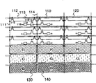
Figure 1A has shown a panel construction, and it is the major part of display unit.On a pixel portion 100 that is positioned at the center, this panel has a data line drive circuit 101.This panel has one and writes scan line drive circuit 102 and one and wipe scan line drive circuit 103 respectively on its left side and the right.Shown in Figure 1B, each pixel has a data wire 111, apply a vision signal (signal of telecommunication) on it, one first scan line (writing scan line) 112, apply one on it and write gate signal, one second scan line (wiping scan line) 113 applies an eraser gate signal on it, a power line (V
(A)) 114, the first film transistor (switching TFT) 115 as switch, second thin-film transistor that is used to wipe (TFT that is used to wipe) 116, the 3rd thin-film transistor (drive TFT) 117 that is used to drive a photophore, described photophore 118, and a counter electrode 119.Can provide a capacitor cell (not shown in Figure 1B) to keep the grid of drive TFT 117 and the voltage between source electrode.Notice that pixel formation of the present invention is not limited to thin-film transistor.It can be a semiconductor device.In the following description, thin-film transistor (TFTs) as a kind of embodiment.
An electrode (the pixel utmost point) of photophore 118 links to each other with source area that drives merit TFT 117 or drain region.One and power line (V
(A)) 114 exist the voltage of potential difference to be applied on another electrode (counter electrode).
Below will be at Figure 1A, circuit drive method of the present invention is described on the basis of 1B and 2B-2D.In the following description, described TFTs has following polarity as a kind of embodiment.Switching TFT 115 and erasing TFT 116 are N channel-styles, and drive TFT 117 is P channel-styles.The electrode that links to each other with the source area or the drain region of drive TFT 117 is an anode, and the described counter electrode in the photophore 119 is a negative electrode.
At first, in an addressing (writing) during the cycle, a pulse is applied to writes scan line 112, produce a H level.Switching TFT 115 is switched on.The vision signal that outputs to data wire 111 is applied to the canopy utmost point of drive TFT 117.
Then, one keep (emission) cycle (display cycle) during, drive TFT 117 is connected.As a result, the potential difference between the current potential of power line 114 and the current potential of count line causes an electric current to flow through photophore 118, has produced light.When drive TFT 117 disconnects, do not have electric current to flow through photophore 118, so it is not luminous.
Then, during a reset cycle, a pulse is applied to wipes scan line 113, produce a H level.Erasing TFT 116 is switched on.When erasing TFT 116 is switched on, the grid of drive TFT 117 and the voltage vanishing between source electrode.Drive TFT 117 is disconnected.The photophore of launching 118 stops emission.After this drive TFT 117 disconnects, be an erase cycle, described therebetween photophore 118 is not luminous.
Each wipes scan line each row execution reset operation just.Therefore, it is consistent being connected on a certain definite pixel of wiping scan line at all the launch time of being controlled by this reset operation.In the present invention, during the cycle of keeping by control photophore 118 the brightness of adjusting RGB launch time.Therefore, in order to control the launch time of R, G, B respectively, shown in Figure 1B with RGB capable and as described in wipe scan line and be arranged in parallel.At this moment, N capable * pixel in the M row by 3N capable * photophore of M row forms.And, be arranged in parallel owing to write scan line and wipe scan line, show that also the RGB row be arranged in parallel with the said write scan line.Therefore, RGB row are arranged in parallel and are called the RGB row for short and are arranged in parallel with described scan line with wiping scan line or write scan line.
Because RGB row are arranged in parallel with described scan line, thus every have only a data wire, one writes scan line and one and wipes scan line.And, can a shared power line between adjacent pixels.With regard to numerical aperture, this is more favourable than disclosed image display device among the JP-A-2001-60076.Because described RGB and scan line are arranged in parallel, the quantity that writes scan line with wipe scan line and equate.Therefore, can drive based on identical clock signal.Therefore, control launch time subsequently is easy.
Hereinafter describe the writing an of input signal of described pixel portion, wherein arrange RGB in mode of the present invention.
Fig. 2 A is that RGB is arranged in an embodiment on the vertical direction.The pixel of the capable M row of N is made up of the photophore of the capable 3M row of N.Like this, write a pixel and finish (shown in frame of broken lines among Fig. 2 A) by writing three RGB points.Write (shown in the frame of broken lines among Fig. 2 A) of delegation's (M pixel=3M point) needs a horizontal cycle.
Fig. 2 B is that RGB is arranged in an embodiment in a lateral direction.The pixel of the capable M row of N is made up of the photophore of the capable M row of 3N.Like this, write a pixel and finish (shown in frame of broken lines among Fig. 2 B) by writing three RGB points.Write (shown in the frame of broken lines among Fig. 2 B) of delegation's (M pixel=3M point) needs three horizontal cycles.The quantity that writes photophore under two kinds of situations equates.Therefore, the length of the length of the former horizontal cycle and three horizontal cycles of the latter is almost equal.
What Fig. 4 represented is a sequential chart of whole operation.In a second, be used in the described light-emitting device show that the image panel of an image is repeatedly shown.At this moment, the flicker when preventing to feel that picture screen rewrites, per second rewrites screen and is considered to necessary for about 60 times, shown in Fig. 4 A.
In addition, in the present invention, adopted the temporal scalability system, therefore a frame period can be divided into a plurality of period of sub-frame.Each period of sub-frame has addressing (a writing) cycle, keeps (emission) cycle for one, a reset cycle and an erase cycle.Classification is finished by the combination of luminous therebetween period of sub-frame.In the example that Fig. 4 A shows, the quantity of gray scale is set to 4bits.A frame period is divided into 4 period of sub-frame SF1 to SF4.Between the length of keeping period T s1 to Ts4 that this period of sub-frame has the ratio of 2 power, for example Ts1: Ts2: Ts3: Ts4=8: 4: 2: 1.So just obtained a linear classification.Certainly, when classification of expression, these ratios are not limited in 2 power.
In Fig. 4 A, the order of the period of sub-frame in frame period has been changed, because should avoid reset cycle overlapping of addressing (writing) cycle and different period of sub-frame.The order that period of sub-frame shows is not limited thereto.
At first, during the addressing period Ta1 of SF1, a vision signal (signal of telecommunication) is written on the picture screen, shown in Fig. 4 B.At this moment, write sequence is as follows: the first row R → first row G → first row B → secondary series R → ... → terminal column R → terminal column G → terminal column B.
Then, forward one to and keep the cycle (launch time).T launch time of R, G, B
R, T
G, R
BBe set to T
R: T
G: T
B=(γ/α): (γ/β): 1, i.e. (1/ α): (1/ β): (1/ γ).Like this, foundation resets and erase cycle according to different colours.Shown in Fig. 4 A, carry out reset operation.At first, in reset cycle ER1, only do wiping on the two field picture about the emitting red light device; Then, in reset cycle EG1, only do wiping on the two field picture about the green emitting device; In other words, launch time of blue-light-emitting device with minimum light transmission rate on the basis red and green launch time with (γ/α) and (coefficient of γ/β) increases.Therefore, the brightness after the transmission is respectively with (γ/α) and (coefficient of γ/β) increases, and can make the brightness after the transmission consistent on RGB.By such control launch time, can make by the brightness after the color layer transmission consistent on RGB.
For example the period of sub-frame SF4 among Fig. 4 A is shorter than addressing period Ta4 place at the cycle of keeping (launch time) Ts4, also carries out wiping and therefore having a reset cycle EB4 of blue-light-emitting device.
Equally, in the present embodiment, the light transmittance of blue color chromatograph is low, and middle as mentioned redness of describing and green launch time are shortened.The invention is not restricted to this method that makes red and green launch time and blue coupling.One might rather say, and characteristics of the present invention are to make launch time and the launch time with colour of minimum light transmission rate to be complementary.
By resetting and can rotate a counter and use this count value to determine the launch time of the RGB of erase cycle control by a door limit clock signal, described clock signal is added to one and writes scan line drive circuit in a write cycle.
In other words, handle during based on the erase cycle that writes the clock signal on the scan line and wipe scan line, and can determine and control the launch time of RGB.
Therefore, in the present invention, the clock signal that writes TFT can be as the clock signal of erasing TFT.Therefore, the present invention has another advantage, and it can easily make time that writes scan line drive circuit and the time of wiping scan line drive circuit be complementary.
(for example (the multiple integral place of the gateable clock signal-count of γ/α) and (γ/β)) can be conspicuous near suitable integer not to be set to use the ratio of color layer light transmittance in launch time.On this basis, can determine and control red (R), green (G), and the launch time of blue (B) look.
In the present embodiment, a kind of situation of light by the color layer transmission described.Also can be applied to the situation of launching different color light by a photophore self by controlling the technological thought of the present invention that constitutes launch time.
Embodiment
Fig. 7,8 and 9 usefulness schematic diagrames have shown the drive circuit of carrying out aforesaid operations.Fig. 7 is the embodiment of a data line drive circuit.Fig. 8 is an embodiment who writes scan line drive circuit.Fig. 9 is an embodiment who wipes scan line drive circuit.
Among Fig. 7, data line drive circuit comprises 703, one level shifters 704 of 702, one second latch cicuits of 710, one first latch cicuits of shift register and the buffer 705 that use multistage trigger 701.
Then, first latch cicuit 702 is according to the input of described sampling pulse receiving digital video signal (numerical data) continuously.When first latch cicuit 702 of final stage is finished the reception of described digital video signal, during a horizontal flyback period, use a latch pulse, simultaneously the digital video signal in first latch cicuit 702 is sent to second latch cicuit 703.
Then, level shifter 704 is carried out the conversion of a voltage to amplitude.This signal is by buffer 705 amplifications and output to data wire S1 to Sm respectively.
Among Fig. 8, write scan line drive circuit and have 810, one level shifters 802 of shift register and a buffer 803 that uses multistage trigger 801.
Then, level shifter 802 is carried out the conversion of a voltage to amplitude.This signal is cushioned device 803 and amplifies.Select to write scan line G in turn
1R, G
1G, G
1B etc. write above-mentioned vision signal in selected hurdle.Select the timing of the time of said write scan line, just in the timing of addressing (writing) in the cycle shown in Figure 10 (top).In Figure 10 (top), G
1R, G
1G, G
1B, G
2R ..., G
nB is the pulse that is used for selecting respectively to write scan line.
Among Fig. 9, the eraser gate signal drive circuit has 902, one buffers 903 of 910, one level shifters of shift register and the multiplexer 904 that use multistage trigger 901.
Three kinds of trigger impulse (G-SP
1, G-SP
2, and G-SP
3) be added to shift register 910.In other words, shift register 910 has three phase places using a common clock signal.According to this clock signal and G-SP
1, from level 1R, 2R, 3R etc. export pulse continuously.According to this clock signal and G-SP
2, from level 1G, 2G, 3G etc. export pulse continuously.According to this clock signal and G-SP
3, from level 1B, 2B, 3B etc. export pulse continuously.Like this, the selection that writes scan line of RGB is regularly independent, and the reset cycle can be set.Subsequently, carry out the conversion of amplitude by level shifter 902.Described pulse is cushioned device 903 amplifications and makes multiplexer 904 at desired time selective erasing scan line.Wipe the selecteed time of scan line, the selection of time in the reset cycle just is shown in Figure 10 (middle part).In Figure 10 (middle part), SR
1R, SR
2R, SR
3R etc., SR
1G, SR
2G, SR
3G etc., and SR
1B, SR
2B, SR
3B etc. are the pulses by described shift register output.GE
1R, GE
2R, GE
3R etc., GE
1G, GE
2G, GE
3G etc., and GE
1B, GE
2B, GE
3B etc. are the pulses that is used for the selective erasing scan line.MPX R, MPX G and MPX B are the signals that is applied to described multiplexer.Wiping the selecteed time of scan line determines.
RGB shown in Figure 10 (bottom) keeps the cycle (launch time) TsR, and TsG and TsB were determined by the reset cycle shown in addressing (writing) cycle shown in Figure 10 (top) and Figure 10 (middle part).Selection of time in the first row pixel is shown in TsR, TsG and TsB.As can be seen, the concluding time of each section launch time is by trigger impulse (G-SP
1To G-SP
3) be added to the described time of wiping scan line drive circuit and determine.At this moment, launch time ratio be (γ/α): (and γ/β): 1, the light transmittance of above-mentioned color layer is α: β: γ.Because can make apparent brightness consistent on RGB, so can show accurate white.
In the present invention, filter is used as concrete color layer.Describe an embodiment, the light transmittance that wherein is used for the filter of RGB is R
R: R
G: R
B=30%: 50%: 20%.
With reference to Fig. 5 A and 5B.Among the present invention, with the same procedure in the aforesaid way, per second is set up 60 frame periods and is shown a 4-bit classification.In execution mode 1, the bit number that 1 frame period equals to show also is divided into four subframe SF
1To SF
4Here, the SF corresponding with most significant bit
1Be further divided into three, just SF1
1, SF1
2, and SF1
3They are arranged mutually discontinuously, and this method produces false contouring when preventing to show intermediate grey scales on the display of EL and so on.False contouring and particulars that solve process are applied among a applicant's the Japanese patent application No.2001-257163.At SF1
1, SF1
2And SF1
3In, used similar vision signal.Therefore, perhaps all photophores are all luminous or not luminous.
In addition, with the same procedure in the aforesaid way, make the order difference that subframe occurs in the different period of sub-frame, thereby prevent the overlapping of addressing (writing) cycle or reset cycle.In other words, if make have long keep the period of sub-frame in (emission) cycle and have the short period of sub-frame of keeping (emission) cycle replace appearance, the problems referred to above will unlikely take place.
Subframe SF
1To SF
4In each all have addressing (a writing) cycle and one and keep (emission) cycle.Here, the light transmittance of blue (B) filter has minimum 20%, thereby the brightness of blue (B) is minimum.Therefore, based on control launch time red (R) of blue (B) and the launch time of green (G).
Utilize make that they respectively are the launch times 67% and 40% of blueness (B) launch time of erase cycle control red (R) and green (G), this launch time can be based on the ratio R of the light transmittance of filter
R: R
G: R
B=30%: 50%: 20% definite.Have minimum light transmission rate, SF owing to pass blueness (B) light of this filter
1To SF
3The erase cycle that has only is used for redness (R) and green (G), in other words, farthest utilizes the launch time of the blueness (B) with minimum brightness.
Owing to following reason, SF4 has red (R) respectively, green (G), and the erase cycle of blue (B) look.The cycle of SF4 is short.Prevented addressing period overlapping of the addressing period of SF4 and next SF2.When showing intermediate grey scales, prevented the generation of dynamic false outline.
In the present embodiment, described an embodiment, realized that wherein driving method of the present invention is different from previously described mode and execution mode 1 and 2.
One of method that is used to drive the active matrix display is a field sequential system, and this is a kind of circumscribed drafting method of human eye temporal resolution that utilized.A coloured image is divided into dissimilar RGB colour informations, according to these colored images that produces continuously.In other words, in an image duration, an image of only being made up of redness, an image and an image of only being made up of blueness of only being made up of green are shown according to this in proper order.Like this,, do not show green and blue image, but different colored image is overlapping on human eye by the after image effect in the moment that a red image is being shown.As a result, this image is hunted down as a coloured image.
Method in the present embodiment is similar to the preceding method operation, briefly, during an addressing (write cycle), at first only writes redness.Then, write green.At last, write blueness.Write emission coloured light in this way respectively.When coloured light required launch time of emission in the past after, carry out similar erase operation.Because (writing) cycle of keeping of emission coloured light overlaps each other, this from the strict sense standard is different from described field sequential system.Here for convenience, this standard is called field sequential system.
A kind of concrete circuit formation and operation are described.Because the formation of data line drive circuit is similar with 2 to previously described mode and execution mode 1 with operation, omit its description here.
Figure 11 has shown a sketch map that scan line drive circuit constitutes.In the present embodiment, writing scan line drive circuit can be similar with wiping scan line drive circuit on constituting.Use the same procedure that writes scan line drive circuit as shown in Figure 8, described scan line drive circuit has 1110, one level shifters 1102 of shift register and the buffer 1103 that use multistage trigger 1101.In addition, it has a selection circuit 1104.
The operation that writes scan line drive circuit in operation from the shift register to the buffer and the execution mode 1 is identical.Export pulse continuously according to a clock signal, a clock inversion signal and a trigger impulse.Here, each to select circuit 1104 be that each output stage for shift register 1110 is provided with.Writing scan line corresponding to three of RGB selects circuit 1104 to link to each other with one.Select circuit 1104 that addressing (a writing) cycle is divided into the phase place front, middle and the back, select the different scan lines that writes in each phase place, and from pulse of shift register output.For example, in the phase place in front, select the scan line that writes, Continuous Selection G corresponding to R
1R, G
2R, G
3R ..., G
nR writes a vision signal with the method.In the phase place of centre, select the scan line that writes, Continuous Selection G corresponding to G
1G, G
2G, G
3G ..., G
nG writes a vision signal in this way.In the phase place of back, select the scan line that writes, Continuous Selection G corresponding to B
1B, G
2B, G
3B ..., G
nB writes a vision signal in this way.This situation is shown in Figure 12 (top).During cycle, trigger impulse has been employed three times in an addressing (writing).
Similarly, after past launch time, carry out erase operation at RGB.This operation is similar to the operation that writes scan line drive circuit.
Because above-described operation, be controlled the launch time of RGB.Wherein, write and wipe according to Figure 12 (top and middle part) and carry out the launch time of above-mentioned color shown in Figure 12 (bottom).
As an example, Fig. 6 shown free embodiment.In this case, the light transmittance of filter is set to R
R: R
G: R
B=30%: 50%: 20%,, identical with method in the execution mode 2 according to the field sequential system executable operations.
Respectively be 67% and 40% of blueness (B) launch time of red (R) and green (G), and the light transmittance here as mentioned above.It is impossible that different colored erase cycle are overlapped each other, and here drive circuit has as shown in figure 11 been realized an erase operation.Thus, carry out to write and erase operation with a kind of preferred order, promptly have bob and penetrate the colour of time and come at first, have long hair and penetrate the colour of time and come at last.
As shown in Figure 6A, in the cycle, the write sequence of launching honorable look is G → R → B in an addressing (writing).Like this, one has the colour of penetrating the time than bob and early comes, and in other words, the launch time that colour of early finishing to write has is shorter than a later colour that writes, therefore must the time of morning be wiped free of at one.Thus, can avoid the overlapping of RGB erase operation as much as possible.
Certainly, design to such an extent that be different from Figure 11 (for example structure of describing in the execution mode 1 as shown in Figure 9) if wipe scan line drive circuit, the overlapping of erase cycle allowed.Yet, use the driving method of describing in structure shown in Figure 11 and the present embodiment here, can make the structure of eraser gate signal drive circuit simpler.
As can be seen, in an addressing period shown in Fig. 6 B, the write time shown in Figure 12 (top) is divided into three line cycles according to different emission light colors.
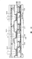
Fig. 3 has shown an embodiment, and wherein the pixel of circuit structure is pressed actual arrangement shown in Figure 1B.Among this figure, 301 is data wires, and 302 are one writes scan line, and 303 are one wipes scan line, 304 be one by the shared power line of adjacent photophore.305 is switching TFT, and 306 is erasing TFT, and 307 is drive TFT, and 308 is pixel electrodes, has omitted emission layer and a counter electrode.Switching TFT 305 and erasing TFT 306 are double gate TFT, and they also can be single control utmost point TFT or control the utmost point (the three or more control utmost point) TFT more.
In the present embodiment, concrete maintenance electric capacity is not set.One keep the cycle during, the voltage between drive TFT 307 grids and source electrode keeps by the path capacitance and the gate capacitance of drive TFT 307 self.
For the said write scan line, use filter and color conversion layer with strip form in the horizontal direction.Because the light of the adjacent photophore emission same color on the left side and the right direction is not so need to copy them.
Execution mode 5
A cross-section structure of light-emitting device of the present invention is briefly described with Figure 13 in the present embodiment.Although show the cross-section structure and the photophore of drive TFT among Figure 13, simple and clear for illustration omitted filter, drier and other structure as the RGB color layer.
In Figure 13,1300 is the substrates with insulating surface, and drive TFT 1310 to 1312 is formed on the substrate 1300, and part semiconductive thin film and the gate electrode of TFT are formed on the substrate 1300.In addition, form from side of substrate: one first insulator film 1301 and one second insulator film 1302 are as the barrier layer, one the 3rd insulator film 1303 is as the door insulator film, one the 4th insulator film 1304 is as passivation film, one the 5th insulator film 1305 is used as the barrier layer as interlayer dielectric film and one the 6th insulator film 1306.In the place that interlayer dielectric film is made by organic material, the 6th insulator film is used to prevent to bleed.
Form in the conduction and connect, and link to each other with the doped region that forms in the active layer of drive TFT 1310-1312.Form the first electrode 1320a-1320c and with described conduction in connect and link to each other.Formation partition wall 1322a-1322c covers in described first electrode and the conduction and connects, and the side of partition wall forms the angle of one 30 to 70 degree.Can on partition wall 1322a-1322c, form in the additional conductive and connect the impedance that reduces first electrode.
Form an organic film (emission layer) 1330 and cover the partition wall 1322a-1322c and the first electrode 1320a-1320c.On organic film (emission layer) 1330, form one second electrode 1331.Should select the material of this second electrode 1331, make it transmit the light of being launched by organic film (emission layer), for example, this electrode is caused by ITO.The laminate patch of the described first electrode 1320a-1320c, organic film (emission layer) 1330 and second electrode 1331 are equivalent to a photophore.
A counter electrode 1350 is arranged on the position corresponding to substrate 1300, and filter 1301R, the 1301G, the 1301B that form on it have the color layer corresponding with photophore.Substrate 1300 and counting substrate 1350 are combined, form a light-emitting device.
In the luminous transposition as shown in figure 13, the light that control is sent by photophore makes it away from substrate 1300 (direction shown in Figure 13 arrow).Therefore described light can carry out multicolor displaying through filter 1301R, 1301G and 1301B.This emission light is called as " end face emission " away from the situation of substrate.In the situation of end face emission, first electrode is equivalent to a negative electrode, and second electrode is equivalent to an anode.
Execution mode 6
Other cross-section structure of light-emitting device of the present invention is briefly described with Figure 14 in the present embodiment.Among Figure 14, since corresponding with the location among Figure 13, so used identical number designation.
A feature of present embodiment is, the position that forms filter 1401R, 1401G, 1401B is below first electrode, and this filter has the color layer corresponding with photophore.Among Figure 14, the joining color layer of end face of formation and the 4th insulator film 1304, its position is not so limited.In other words, color layer can be below first electrode.The installation site can suitably be set.
Since reasons in structure, the light Be Controlled directive substrate 1300 (direction shown in Figure 14 arrow) that the photophore in Figure 14 light-emitting device sends.Therefore, should select the material of second electrode, make it transmit the light of being launched by organic film (emission layer), for example, this electrode is caused by ITO.The situation of this emission light directive substrate is called as " lower surface emission ".In the situation of lower surface emission, first electrode is equivalent to an anode, and second electrode is equivalent to a negative electrode.
In the situation of present embodiment lower surface emission, using pixel of the present invention to arrange the place of (Fig. 1), the quantity of power line can be halved.Therefore, have a multiplier effect, it obtains a high-NA.
Execution mode 7
At last, an embodiment who obtains white light emission is described.The method that obtains white light emission comprises the mixture of colours that adds shown in Figure 15 A, the emission layer that will be used to produce three primary colors light R (red), G (green), B (indigo plant) in this method pile up add and mixes shown in colour; The method that has also comprised a kind of utilization shown in Figure 15 B and concern between two complementary colors.In the place of using complementary color, the combination of blue-yellow or viridescent-orange is known.Because can utilize the light emission in the higher visual sensitivity wave-length coverage, it is especially useful that the latter is considered to.
Execution mode 8
Use the electronic equipment of light-emitting device of the present invention to comprise, for example, video camera, digital camera, glasses type displayer (wearing overhead display), navigation system, audio playback (for example automobile audio and audio-frequency assembly), notebook computer, game machine, personal digital assistant device (for example removable computer, mobile phone, portable game machine and e-book), and is furnished with recording medium (especially, a kind of recording medium is the transcriber of digital video disk (DVD) for example, it comprise one can display image display) the copying image device.Especially, with regard to personal digital assistant device, owing to be provided with a high priority on the width of visual angle, the portable data assistance more from the viewed possibility of incline direction preferably uses this light-emitting device.The example that has shown practical application among Figure 16 A-16H.In addition, the electronic equipment of giving an example in this specification is embodiment, so the present invention in particular but and non-exclusively be applicable to these embodiment.
Figure 16 A has shown a light-emitting device, and it comprises a shell 2001, support base 2002, display part 2003, speaker portion 2004, a video inputs or the like.Light-emitting device of the present invention can be applied to display part 2003.In addition, the light-emitting device shown in Figure 16 A has comprised the present invention.Because this emitter is the self-luminous type, it does not need a bias light, and therefore can obtain a display part thinner than LCD.Notice that this light-emitting device comprises all information displays, for example, PC, television broadcasting transmitter-receiver and advertisement display.
Figure 16 B has shown a digital camera, and it comprises strong 2104, external-connected ports of a fuselage 2101, display part 2102, image receiving unit 2103, operation 2105, a shutter 2106 or the like.Light-emitting device of the present invention can be applied to display part 2102.In addition, the digital camera shown in Figure 16 B has comprised the present invention.
Figure 16 C has shown a notebook computer, and it comprises a fuselage 2201, shell 2202, display part 2203, keyboard 2204, external-connected port 2205, an indication mouse 2206 or the like.Light-emitting device of the present invention can be applied to display part 2203.In addition, the light-emitting device shown in Figure 16 C has comprised the present invention.
Figure 16 D has shown a removable computer, and it comprises a fuselage 2301, display part 2302, switch 2303, operation keys 2304, an infrared port 2305 or the like.Light-emitting device of the present invention can be applied to display part 2303.In addition, the removable computer shown in Figure 16 D has comprised the present invention.
Figure 16 E has shown that one is furnished with recording medium (especially, a DVD reproducing unit) portable image reproducing unit, it comprises that a fuselage 2401, shell 2402, display part A 2403, display part B 2404, recording medium (for example DVD) reads in part 2405, operation keys 2406, a speaker portion 2407 or the like.Display part A 2403 main displays image information, display part B 2404 main character display information.Light-emitting device of the present invention can be applied among display part A 2403 and the display part B2404.Notice that home game machine etc. are included in the described copying image device of being furnished with recording medium.In addition, the DVD reproducing unit shown in Figure 16 E has comprised the present invention.
Figure 16 F has shown the display (wearing overhead display) of a goggles type, and it comprises a fuselage 2501, display part 2502, a support arm portion 2503 or the like.Light-emitting device of the present invention can be used in the display part 2502.The display of the goggles type shown in Figure 16 F has comprised the present invention.
Figure 16 G has shown a video camera, it comprises a fuselage 2601, display part 2602, shell 2603, external-connected port 2604, remote control receiving unit 2605, an image receiving unit 2606, a battery 2607, an audio input end 2608,2609, one eyepiece parts 2610 of operation keys or the like.Light-emitting device of the present invention can use in display part 2602.Video camera shown in Figure 16 G has comprised the present invention.
Here, Figure 16 H has shown a mobile phone, and it comprises a fuselage 2701, shell 2702, display part 2703, audio input end 2704, audio output 2705, operation keys 2706, external-connected port 2707, an antenna 2708 or the like.Light-emitting device of the present invention can use in display part 2703.Note,, can suppress the current drain of mobile phone by display white character on a black background.In addition, the mobile phone shown in Figure 16 H has comprised the present invention.
When increasing the emission brightness of luminescent material, this light-emitting device can be applied to the projector of a front or back side type, and these projector scioptics or the amplification of similar device and projection comprise the output light of image information.
Above-mentioned electronic equipment shows through the example of electricity in the information of communication line such as Internet and CATV (cable TV) distribution to be increased, and especially shows dynamic image.Because the response speed of luminescent material is very high, this luminous transposition is more suitable for being used for dynamic image and shows.
Because light-emitting device consumed power in luminous component, so reduce luminous component when wishing display message as much as possible, therefore, when light-emitting device is used to the display part of a personal digital assistant device, especially mobile phone, voice reproducing device etc., its main character display information, it is more suitable forming described character information in having the luminous component of Background luminescence not.
As mentioned above, range of application of the present invention is very extensive, so the present invention can be used for the electronic equipment of all spectra.Can use the structure of any one light-emitting device in the execution mode 1 to 6 according to the electronic equipment of present embodiment.
Claims (28)
1. a light-emitting device has a pixel portion, a plurality of data wires, a plurality of first scan lines and a plurality of second scan line;
Wherein this pixel portion has the pixel with arranged,
Each pixel comprises first photophore of emission first coloured light, second photophore of emission second coloured light, the 3rd photophore of emission the 3rd coloured light, the power line that be arranged in parallel with data wire, the first transistor between first photophore and power line, transistor seconds between second photophore and power line, and the 3rd transistor between the 3rd photophore and power line;
Wherein said first photophore, second photophore and the 3rd photophore are arranged in the row and the major axis and described first scan line of described first photophore, second photophore and the 3rd photophore be arranged in parallel; And
First coloured light: second coloured light: the beam intensity ratio of the 3rd coloured light is α: β: γ, and when this light-emitting device display white, first photophore: second photophore: ratio launch time of the 3rd photophore is 1/ α: 1/ β: 1/ γ.
2. light-emitting device as claimed in claim 1, wherein first coloured light, second coloured light and the 3rd coloured light are obtained by filter or color conversion layer by monochromatic light.
3. light-emitting device as claimed in claim 1, wherein first coloured light, second coloured light and the 3rd coloured light are obtained by the luminescent material of emission first coloured light, second coloured light and the 3rd coloured light respectively.
4. electronic installation uses light-emitting device as claimed in claim 1.
5. a light-emitting device has a pixel portion;
Wherein this pixel portion has the pixel with arranged,
Each pixel comprises first photophore of emission first coloured light, second photophore of emission second coloured light, the 3rd photophore of emission the 3rd coloured light, and power line;
In wherein said first photophore, second photophore and the 3rd photophore each all has a data wire, one first scan line, one second scan line, a first transistor, a transistor seconds and one the 3rd transistor;
The first transistor has a gate electrode, is electrically connected with corresponding first scanning line;
Transistor seconds has a gate electrode, with corresponding second scan line electrical connection;
The 3rd transistor has a gate electrode, with the source area of corresponding the first transistor or drain region be electrically connected;
One in the 3rd transistorized source area or drain region and first photophore, second photophore and the 3rd photophore is electrically connected, and another of the 3rd transistorized source area or drain region is electrically connected with power line;
Wherein, power line and data wire be arranged in parallel;
The major axis and the corresponding first scanning line of first photophore, second photophore and the 3rd photophore be arranged in parallel; And
First coloured light: second coloured light: the beam intensity ratio of the 3rd coloured light is α: β: γ, and when this light-emitting device display white, first photophore: second photophore: ratio launch time of the 3rd photophore is 1/ α: 1/ β: 1/ γ.
6. light-emitting device as claimed in claim 5, wherein first coloured light, second coloured light and the 3rd coloured light are obtained by filter or color conversion layer by monochromatic light.
7. light-emitting device as claimed in claim 5, wherein first coloured light, second coloured light and the 3rd coloured light are obtained by the luminescent material of emission first coloured light, second coloured light and the 3rd coloured light respectively.
8. electronic installation uses light-emitting device as claimed in claim 5.
9. a light-emitting device has a pixel portion;
Wherein this pixel portion has the pixel with arranged,
Each pixel comprises first photophore of emission first coloured light, the 3rd photophore of second photophore of emission second coloured light and emission the 3rd coloured light;
In wherein said first photophore, second photophore and the 3rd photophore each all has a data wire, one first scan line, one second scan line, a power line, a first transistor, a transistor seconds and one the 3rd transistor;
The first transistor has a gate electrode, is electrically connected with corresponding first scanning line;
Transistor seconds has a gate electrode, with corresponding second scan line electrical connection;
The 3rd transistor has a gate electrode, with the source area of corresponding the first transistor or drain region be electrically connected;
In the 3rd transistorized source area and the drain region one is electrically connected with shared power line, another then with first photophore, second photophore and the 3rd photophore in one be electrically connected;
The major axis and the corresponding first scanning line of first photophore, second photophore and the 3rd photophore be arranged in parallel;
Wherein, power line and data wire be arranged in parallel;
First photophore, second photophore and the 3rd photophore provide electric current by shared power line; With
First coloured light: second coloured light: the beam intensity ratio of the 3rd coloured light is α: β: γ, and when this light-emitting device display white, first photophore: second photophore: ratio launch time of the 3rd photophore is 1/ α: 1/ β: 1/ γ.
10. light-emitting device as claimed in claim 9, wherein first coloured light, second coloured light and the 3rd coloured light are obtained by filter or color conversion layer by monochromatic light.
11. light-emitting device as claimed in claim 9, wherein first coloured light, second coloured light and the 3rd coloured light are obtained by the luminescent material of emission first coloured light, second coloured light and the 3rd coloured light respectively.
12. electronic installation uses light-emitting device as claimed in claim 9.
13. a light-emitting device has a pixel portion;
Wherein this pixel portion has the pixel with arranged,
Each pixel comprises first photophore of an emission red (R) light, the 3rd photophore of second photophore of an emission green (G) light and blue (B) light of emission;
In wherein said first photophore, second photophore and the 3rd photophore each all has a data wire, one first scan line, one second scan line, a power line, a first transistor, a transistor seconds and one the 3rd transistor;
The first transistor has a gate electrode, is electrically connected with corresponding first scanning line;
Transistor seconds has a gate electrode, with corresponding second scan line electrical connection;
The 3rd transistor has a gate electrode, with the source area of corresponding the first transistor or drain region be electrically connected;
In the 3rd transistorized source area and the drain region one is electrically connected with shared power line, another then with first photophore, second photophore and the 3rd photophore in one be electrically connected;
The major axis and the corresponding first scanning line of first photophore, second photophore and the 3rd photophore be arranged in parallel;
Wherein, power line and data wire be arranged in parallel;
First photophore, second photophore and the 3rd photophore provide electric current by shared power line; With
Red (R) light: green (G) light: the beam intensity ratio of blue (B) light is α: β: γ, and when this light-emitting device display white first photophore: second photophore: ratio launch time of the 3rd photophore is 1/ α: 1/ β: 1/ γ.
14. light-emitting device as claimed in claim 13, wherein red (R) light, green (G) light and indigo plant (B) light are obtained by filter or color conversion layer by monochromatic light.
15. light-emitting device as claimed in claim 13, wherein red (R) light, green (G) light and indigo plant (B) light are obtained by the luminescent material of emission red (R) light, green (G) light and indigo plant (B) light respectively.
16. electronic installation uses light-emitting device as claimed in claim 13.
17. a light-emitting device comprises:
One first writes scan line, extends upward in first party;
Wipe scan line, extend upward for one first in described first party;
A data wire extends on the direction of intersecting with described first direction;
One second writes scan line, extends upward in described first party;
Wipe scan line, extend upward for one second in described first party;
One the 3rd writes scan line, extends upward in described first party;
Wipe scan line for one the 3rd, extend upward in described first party;
A power line is parallel to described data wire and extends;
One writes first sub-pixel that scan line, first is wiped the definition of scan line and data wire by described first;
One writes second sub-pixel that scan line, second is wiped the definition of scan line and data wire by described second;
One writes the 3rd sub-pixel that scan line, the 3rd is wiped the definition of scan line and data wire by the described the 3rd;
One first photophore in this first sub-pixel, one first coloured light of this first photophore emission;
One second photophore in this second sub-pixel, second coloured light that is different from first coloured light of this second photophore emission;
One the 3rd photophore in the 3rd sub-pixel, the 3rd coloured light that is different from first coloured light and second coloured light of the 3rd photophore emission;
In described first photophore, second photophore and the 3rd photophore each comprises at least one the first transistor, a transistor seconds and one the 3rd transistor, and wherein the first transistor gate electrode is electrically connected with the corresponding scan line that writes; Gate electrode of transistor seconds is electrically connected with the corresponding scan line of wiping, and the 3rd a transistorized gate electrode is electrically connected with the source electrode or the drain region of the first transistor; The 3rd transistorized source area or drain region and corresponding photophore are electrically connected, and another of the 3rd transistorized source area or drain region is electrically connected with power line and
First coloured light: second coloured light: the beam intensity ratio of the 3rd coloured light is α: β: γ, and when this light-emitting device display white, first photophore: second photophore: ratio launch time of the 3rd photophore is 1/ α: 1/ β: 1/ γ.
18. light-emitting device as claimed in claim 17, wherein first coloured light, second coloured light and the 3rd coloured light are obtained by filter or color conversion layer by monochromatic light.
19. light-emitting device as claimed in claim 17, wherein first coloured light, second coloured light and the 3rd coloured light are obtained by the luminescent material of emission first coloured light, second coloured light and the 3rd coloured light respectively.
20. electronic installation uses light-emitting device as claimed in claim 17.
21. the method for a driven for emitting lights device, this light-emitting device have a pixel portion, a plurality of data wires, a plurality of first scan lines and a plurality of second scan line;
Wherein this pixel portion has the pixel with arranged,
Described pixel comprises first photophore of launching first coloured light, launch second photophore of second coloured light, the 3rd photophore with emission the 3rd coloured light, the power line that be arranged in parallel with data wire, the first transistor between first photophore and power line, transistor seconds between second photophore and power line, and the 3rd transistor between the 3rd photophore and power line; And
Wherein said first photophore, second photophore and the 3rd photophore are arranged in the row, and the major axis of described first photophore, second photophore and the 3rd photophore and described first scan line be arranged in parallel;
This method comprises the step of controlling launch time, if thereby first coloured light: second coloured light: the beam intensity ratio of the 3rd coloured light is α: β: γ, when this light-emitting device display white, first photophore: second photophore: ratio launch time of the 3rd photophore is 1/ α: 1/ β: 1/ γ.
22. electronic installation uses the method for driven for emitting lights device as claimed in claim 21.
23. the method for a driven for emitting lights device, this light-emitting device have a pixel portion, a plurality of data wires, a plurality of first scan lines, and a plurality of second scan line;
Wherein pixel portion has the pixel with arranged,
Described pixel comprises first photophore of launching first coloured light, launch second photophore of second coloured light, and the 3rd photophore of launching the 3rd coloured light, the power line that be arranged in parallel with data wire, the first transistor between first photophore and power line, transistor seconds between second photophore and power line, and the 3rd transistor between the 3rd photophore and power line; And
Wherein said first photophore, second photophore and the 3rd photophore are arranged in the row, and the major axis of described first photophore, second photophore and the 3rd photophore and described first scan line be arranged in parallel;
This method may further comprise the steps:
Be applied to first photophore corresponding to one by described data wire, the lock in time of the vision signal of second photophore and the 3rd photophore, set up a frame period, and obtain a plurality of period of sub-frame by dividing this frame period, each period of sub-frame has a described vision signal and is written into first photophore, phase place during second photophore and the 3rd photophore, one first photophore, second photophore and the 3rd photophore respond the phase place during this vision signal is launched, and one first photophore, phase place during second photophore and the 3rd photophore stop to launch; With
Control launch time, if thereby first coloured light: second coloured light: the beam intensity ratio of the 3rd coloured light is α: β: γ, then when this light-emitting device display white, first photophore: second photophore: ratio launch time of the 3rd photophore is 1/ α: 1/ β: 1/ γ.
24. electronic installation uses the method for driven for emitting lights device as claimed in claim 23.
25. the method for a driven for emitting lights device, this light-emitting device have a pixel portion, a plurality of data wires, a plurality of first scan lines and a plurality of second scan line;
Wherein pixel portion has the pixel with arranged,
Described pixel comprises first photophore of launching first coloured light, launch second photophore of second coloured light, and the 3rd photophore of launching the 3rd coloured light, the power line that be arranged in parallel with data wire, the first transistor between first photophore and power line, transistor seconds between second photophore and power line, and the 3rd transistor between the 3rd photophore and power line; And
Wherein first photophore, second photophore and the 3rd photophore are arranged in the row, and the major axis of described first photophore, second photophore and the 3rd photophore and described first scan line be arranged in parallel;
This method may further comprise the steps:
In any delegation of a selected state of first scan line, a vision signal is write first photophore, second photophore and the 3rd photophore;
Allow first photophore, second photophore and the 3rd photophore respond this vision signal and launch; With
Control launch time, if thereby first coloured light: second coloured light: the beam intensity ratio of the 3rd coloured light is α: β: γ, then when by closing first photophore, second photophore and the 3rd photophore simultaneously when making this light-emitting device display white, first photophore: second photophore: ratio launch time of the 3rd photophore is 1/ α: 1/ β: 1/ γ.
26. electronic installation uses the method for driven for emitting lights device as claimed in claim 25.
27. the method for a driven for emitting lights device, this light-emitting device have a pixel portion, a plurality of data wires, a plurality of first scan lines, and a plurality of second scan line;
Wherein pixel portion has the pixel with arranged,
Described pixel comprises first photophore of launching first coloured light, launches second photophore of second coloured light, and the 3rd photophore of launching the 3rd coloured light;
Wherein first photophore, second photophore and the 3rd photophore are arranged in the row, and the major axis of described first photophore, second photophore and the 3rd photophore and described first scan line be arranged in parallel;
This method may further comprise the steps:
Carry out first step, first vision signal is write first photophore;
Carry out second step, second vision signal is write second photophore;
Carry out third step, the 3rd vision signal is write the 3rd photophore;
Carry out the 4th step, close first photophore, make it not luminous;
Carry out the 5th step, close second photophore, make it not luminous;
Carry out the 6th step, close the 3rd photophore, make it not luminous;
Wherein a plurality of first vision signals are write a plurality of first photophores simultaneously, described a plurality of first photophore is connected to the same of a plurality of first scan lines, a plurality of second vision signals are write a plurality of second photophores simultaneously, described a plurality of second photophore is connected to the same of a plurality of first scan lines, a plurality of the 3rd vision signals are write a plurality of the 3rd photophores simultaneously, and described a plurality of the 3rd photophores are connected to the same of a plurality of first scan lines;
Wherein close a plurality of first photophores and carry out simultaneously, described a plurality of first photophores are connected to the same of a plurality of second scan lines; Close a plurality of second photophores and carry out simultaneously, described a plurality of second photophores are connected to the same of a plurality of second scan lines; Close a plurality of the 3rd photophores and carry out simultaneously, described a plurality of the 3rd photophores are connected to the same of a plurality of second scan lines; With
Control launch time, if thereby first coloured light: second coloured light: the beam intensity ratio of the 3rd coloured light is α: β: γ, then when making this light-emitting device display white by the time of controlling the 4th step, the 5th step and the 6th step independent startup, first photophore: second photophore: ratio launch time of the 3rd photophore is 1/ α: 1/ β: 1/ γ.
28. electronic installation uses the method for driven for emitting lights device as claimed in claim 27.
Applications Claiming Priority (2)
| Application Number | Priority Date | Filing Date | Title |
|---|---|---|---|
| JP2002070587 | 2002-03-14 | ||
| JP2002070587A JP3957535B2 (en) | 2002-03-14 | 2002-03-14 | Driving method of light emitting device, electronic device |
Publications (2)
| Publication Number | Publication Date |
|---|---|
| CN1450509A CN1450509A (en) | 2003-10-22 |
| CN100455028C true CN100455028C (en) | 2009-01-21 |
Family
ID=28035069
Family Applications (1)
| Application Number | Title | Priority Date | Filing Date |
|---|---|---|---|
| CNB031107397A Expired - Fee Related CN100455028C (en) | 2002-03-14 | 2003-03-13 | Lighting apparatus and driving method |
Country Status (3)
| Country | Link |
|---|---|
| US (2) | US7250931B2 (en) |
| JP (1) | JP3957535B2 (en) |
| CN (1) | CN100455028C (en) |
Families Citing this family (51)
| Publication number | Priority date | Publication date | Assignee | Title |
|---|---|---|---|---|
| US7042162B2 (en) | 2002-02-28 | 2006-05-09 | Semiconductor Energy Laboratory Co., Ltd. | Light emitting device |
| US7023141B2 (en) * | 2002-03-01 | 2006-04-04 | Semiconductor Energy Laboratory Co., Ltd. | Light emitting device and drive method thereof |
| US7218298B2 (en) * | 2002-04-03 | 2007-05-15 | Semiconductor Energy Laboratory Co., Ltd. | Light emitting device |
| US7081704B2 (en) * | 2002-08-09 | 2006-07-25 | Semiconductor Energy Laboratory Co., Ltd. | Semiconductor device and manufacturing method thereof |
| CN100403382C (en) * | 2002-09-16 | 2008-07-16 | 皇家飞利浦电子股份有限公司 | Active matrix display with variable duty cycle |
| JP2004145300A (en) | 2002-10-03 | 2004-05-20 | Seiko Epson Corp | Electronic circuit, method for driving electronic circuit, electronic device, electrooptical device, method for driving electrooptical device, and electronic apparatus |
| KR100959775B1 (en) * | 2003-09-25 | 2010-05-27 | 삼성전자주식회사 | Scan driver, flat panel display device having the same, and method for driving thereof |
| JP4566545B2 (en) * | 2003-10-24 | 2010-10-20 | 大日本印刷株式会社 | Time-division gradation display drive, time-division gradation display |
| WO2005050603A1 (en) * | 2003-11-19 | 2005-06-02 | Shinya Ishida | Chained led module |
| KR100686343B1 (en) * | 2003-11-29 | 2007-02-22 | 삼성에스디아이 주식회사 | Organic electro luminescence display |
| JP4569107B2 (en) * | 2004-01-06 | 2010-10-27 | ソニー株式会社 | Display device and driving method of display device |
| JP2006023585A (en) * | 2004-07-08 | 2006-01-26 | Rohm Co Ltd | Method for driving display device and display device using the same |
| EP1622111A1 (en) * | 2004-07-28 | 2006-02-01 | Deutsche Thomson-Brandt Gmbh | Line driver circuit for active matrix display device |
| US20060038752A1 (en) * | 2004-08-20 | 2006-02-23 | Eastman Kodak Company | Emission display |
| JP2006058770A (en) * | 2004-08-23 | 2006-03-02 | Toshiba Matsushita Display Technology Co Ltd | Driving circuit for display apparatus |
| JP4510735B2 (en) | 2004-09-22 | 2010-07-28 | 統寶光電股▲ふん▼有限公司 | Design method, panel and its electronic device |
| JP2006275571A (en) * | 2005-03-28 | 2006-10-12 | Ricoh Elemex Corp | Digital clock |
| US20060076567A1 (en) * | 2004-09-24 | 2006-04-13 | Keisuke Miyagawa | Driving method of light emitting device |
| KR20060076041A (en) * | 2004-12-29 | 2006-07-04 | 엘지.필립스 엘시디 주식회사 | Organic light-emitting diode display device |
| JP2006259530A (en) * | 2005-03-18 | 2006-09-28 | Seiko Epson Corp | Organic el device, driving method thereof, and electronic device |
| JP2006276099A (en) * | 2005-03-28 | 2006-10-12 | Tohoku Pioneer Corp | Apparatus and method for driving light emitting display panel |
| DE102006014873B4 (en) * | 2005-03-31 | 2019-01-03 | Lg Display Co., Ltd. | Driving method for an electroluminescent display device |
| US8619007B2 (en) | 2005-03-31 | 2013-12-31 | Lg Display Co., Ltd. | Electro-luminescence display device for implementing compact panel and driving method thereof |
| KR101213937B1 (en) * | 2005-04-18 | 2012-12-18 | 엘지디스플레이 주식회사 | Electro-luminescence display device |
| JP4692996B2 (en) * | 2005-09-27 | 2011-06-01 | 株式会社 日立ディスプレイズ | Display device |
| JP4991138B2 (en) * | 2005-10-20 | 2012-08-01 | 株式会社ジャパンディスプレイセントラル | Driving method and driving apparatus for active matrix display device |
| KR20070043314A (en) * | 2005-10-21 | 2007-04-25 | 삼성전자주식회사 | Liquid crystal display |
| KR100804639B1 (en) * | 2005-11-28 | 2008-02-21 | 삼성전자주식회사 | Method for driving display device |
| JP2007157404A (en) * | 2005-12-01 | 2007-06-21 | Seiko Epson Corp | Display device and electronic equipment |
| US20090153462A1 (en) * | 2005-12-08 | 2009-06-18 | Sharp Kabushiki Kaisha | Illumination device and display apparatus provided with the same |
| JP2007272203A (en) * | 2006-03-06 | 2007-10-18 | Nec Corp | Display apparatus |
| EP1873744A1 (en) * | 2006-06-30 | 2008-01-02 | Deutsche Thomson Brandt | Active matrix organic light emitting display (amoled) device |
| JP4968857B2 (en) * | 2006-08-07 | 2012-07-04 | パイオニア株式会社 | Pixel driving apparatus and pixel driving method |
| WO2008018449A1 (en) | 2006-08-09 | 2008-02-14 | Sharp Kabushiki Kaisha | Liquid crystal display device |
| WO2008065766A1 (en) * | 2006-11-29 | 2008-06-05 | Sharp Kabushiki Kaisha | Backlight device, display, and television receiver |
| WO2008123403A1 (en) | 2007-04-02 | 2008-10-16 | Sharp Kabushiki Kaisha | Illuminator and display having same |
| WO2008129998A1 (en) * | 2007-04-20 | 2008-10-30 | Sharp Kabushiki Kaisha | Lighting system and display device equipped with the same |
| CN101821797A (en) * | 2007-10-19 | 2010-09-01 | 株式会社半导体能源研究所 | Display device and method for driving thereof |
| TWI400680B (en) * | 2008-09-30 | 2013-07-01 | Innolux Corp | Method for driving backlight module and display |
| TWI420493B (en) * | 2009-12-17 | 2013-12-21 | Au Optronics Corp | Gate driving circuit |
| GB2504260B (en) * | 2012-05-23 | 2020-01-08 | Flexenable Ltd | Electronic display |
| EP2852948A1 (en) | 2012-05-23 | 2015-04-01 | Plastic Logic Limited | Electronic display |
| CN102866551B (en) * | 2012-10-11 | 2015-04-15 | 深圳市华星光电技术有限公司 | Liquid-crystal display device and driving circuit thereof |
| KR101999560B1 (en) * | 2012-11-28 | 2019-07-15 | 삼성디스플레이 주식회사 | Organic light emittign display device |
| KR20140137243A (en) * | 2013-05-22 | 2014-12-02 | 삼성디스플레이 주식회사 | Display device and display device driving mtehod |
| TWI559275B (en) | 2015-02-09 | 2016-11-21 | 財團法人工業技術研究院 | Pixel driving method and associated display device |
| CN105118430B (en) * | 2015-08-31 | 2018-05-25 | 上海和辉光电有限公司 | Pixel-driving circuit and its driving method and display device |
| US10797113B2 (en) * | 2016-01-25 | 2020-10-06 | Semiconductor Energy Laboratory Co., Ltd. | Light-emitting device with layered electrode structures |
| US10026348B2 (en) * | 2016-03-11 | 2018-07-17 | Apple Inc. | Driving scheme for high brightness and fast response panel flash |
| JP2020060756A (en) * | 2018-10-09 | 2020-04-16 | セイコーエプソン株式会社 | Electro-optical device and electronic apparatus |
| US10991319B2 (en) | 2018-10-09 | 2021-04-27 | Seiko Epson Corporation | Electro-optical device and electronic apparatus |
Citations (5)
| Publication number | Priority date | Publication date | Assignee | Title |
|---|---|---|---|---|
| JPH07175439A (en) * | 1993-12-17 | 1995-07-14 | Fujitsu General Ltd | Driving method for display device |
| CN1278635A (en) * | 1999-06-17 | 2001-01-03 | 索尼公司 | Image displaying apparatus |
| CN1290041A (en) * | 1999-09-24 | 2001-04-04 | 株式会社半导体能源研究所 | Electroluminescent display unit and electronic device |
| JP2001142427A (en) * | 1999-11-16 | 2001-05-25 | Pioneer Electronic Corp | Matrix type display device and its driving method |
| JP2002032051A (en) * | 2000-07-18 | 2002-01-31 | Sony Corp | Display device and its driving method, and portable terminal |
Family Cites Families (40)
| Publication number | Priority date | Publication date | Assignee | Title |
|---|---|---|---|---|
| DE3203986A1 (en) * | 1982-02-05 | 1983-08-18 | Robert Bosch Gmbh, 7000 Stuttgart | METHOD FOR MEASURING THE FLOW OF A MEDIUM |
| EP0189214B1 (en) * | 1985-01-25 | 1997-07-23 | Nec Corporation | Liquid-crystal multi-color display panel structure |
| DE3724086A1 (en) * | 1986-07-22 | 1988-02-04 | Sharp Kk | DRIVER CIRCUIT FOR A THREE-LAYER ELECTROLUMINESCENT DISPLAY |
| JP2738704B2 (en) | 1988-06-20 | 1998-04-08 | 株式会社日立製作所 | Liquid crystal display |
| GB8909011D0 (en) * | 1989-04-20 | 1989-06-07 | Friend Richard H | Electroluminescent devices |
| JP2725071B2 (en) | 1990-03-09 | 1998-03-09 | 富士通株式会社 | Magnetic disk drive |
| JPH03259388A (en) | 1990-03-09 | 1991-11-19 | Nec Corp | Graphic structure data display device with stuffing fair copying function |
| JP2784615B2 (en) * | 1991-10-16 | 1998-08-06 | 株式会社半導体エネルギー研究所 | Electro-optical display device and driving method thereof |
| US5714968A (en) * | 1994-08-09 | 1998-02-03 | Nec Corporation | Current-dependent light-emitting element drive circuit for use in active matrix display device |
| US6078304A (en) * | 1994-10-24 | 2000-06-20 | Miyazawa; Kuniaki | Panel type color display device and system for processing image information |
| US5652600A (en) * | 1994-11-17 | 1997-07-29 | Planar Systems, Inc. | Time multiplexed gray scale approach |
| JPH1039791A (en) | 1996-07-22 | 1998-02-13 | Mitsubishi Electric Corp | Organic electroluminescence display device |
| DE69739633D1 (en) * | 1996-11-28 | 2009-12-10 | Casio Computer Co Ltd | display device |
| TW441136B (en) * | 1997-01-28 | 2001-06-16 | Casio Computer Co Ltd | An electroluminescent display device and a driving method thereof |
| KR100544821B1 (en) * | 1997-02-17 | 2006-01-24 | 세이코 엡슨 가부시키가이샤 | Organic electroluminescence device |
| WO1998048322A1 (en) * | 1997-04-22 | 1998-10-29 | Matsushita Electric Industrial Co., Ltd. | Liquid crystal display with image reading function, image reading method and manufacturing method |
| JPH1115450A (en) * | 1997-06-27 | 1999-01-22 | Sony Corp | Display device |
| JP2000227784A (en) | 1998-07-29 | 2000-08-15 | Seiko Epson Corp | Driving circuit for electro-optical device, and electro- optical device |
| JP2000092520A (en) * | 1998-09-16 | 2000-03-31 | Toshiba Corp | Stereoscopic video display device |
| JP3663941B2 (en) * | 1998-09-28 | 2005-06-22 | 三菱電機株式会社 | Spectral sensitivity characteristic measuring method and imaging data construction method of imaging apparatus |
| US6274887B1 (en) | 1998-11-02 | 2001-08-14 | Semiconductor Energy Laboratory Co., Ltd. | Semiconductor device and manufacturing method therefor |
| JP3686769B2 (en) * | 1999-01-29 | 2005-08-24 | 日本電気株式会社 | Organic EL element driving apparatus and driving method |
| JP2001102626A (en) * | 1999-07-28 | 2001-04-13 | Canon Inc | Led chip, led chip array, led array head and imaging apparatus |
| JP4906017B2 (en) | 1999-09-24 | 2012-03-28 | 株式会社半導体エネルギー研究所 | Display device |
| TW480727B (en) * | 2000-01-11 | 2002-03-21 | Semiconductor Energy Laboratro | Semiconductor display device |
| TW495808B (en) * | 2000-02-04 | 2002-07-21 | Semiconductor Energy Lab | Thin film formation apparatus and method of manufacturing self-light-emitting device using thin film formation apparatus |
| JP4785257B2 (en) | 2000-02-04 | 2011-10-05 | 株式会社半導体エネルギー研究所 | Method for manufacturing light emitting device |
| JP2001257163A (en) | 2000-03-10 | 2001-09-21 | Kyocera Corp | Silicon carbide member, plasma-resistant member, and semiconductor manufacturing device |
| JP4884592B2 (en) | 2000-03-15 | 2012-02-29 | 株式会社半導体エネルギー研究所 | Method for manufacturing light emitting device and method for manufacturing display device |
| US6706544B2 (en) | 2000-04-19 | 2004-03-16 | Semiconductor Energy Laboratory Co., Ltd. | Light emitting device and fabricating method thereof |
| JP2002032057A (en) | 2000-05-08 | 2002-01-31 | Semiconductor Energy Lab Co Ltd | Light emitting device and driving method therefor |
| US6989805B2 (en) | 2000-05-08 | 2006-01-24 | Semiconductor Energy Laboratory Co., Ltd. | Light emitting device |
| TW521256B (en) | 2000-05-18 | 2003-02-21 | Semiconductor Energy Lab | Electronic device and method of driving the same |
| JP4683766B2 (en) | 2000-05-22 | 2011-05-18 | 株式会社半導体エネルギー研究所 | Active matrix light emitting device |
| TW536836B (en) | 2000-05-22 | 2003-06-11 | Semiconductor Energy Lab | Light emitting device and electrical appliance |
| US6809470B2 (en) * | 2000-12-29 | 2004-10-26 | Intel Corporation | Flat panel color display with enhanced brightness and preferential viewing angles |
| US7034801B2 (en) * | 2001-01-10 | 2006-04-25 | Mitsubishi Denki Kabushiki Kaisha | Color image display |
| US6860296B2 (en) * | 2001-06-27 | 2005-03-01 | Winston B. Young | High flow nozzle system for flow control in bladder surge tanks |
| JP2003131619A (en) | 2001-10-25 | 2003-05-09 | Toshiba Corp | Self light emitting type display device |
| US7218298B2 (en) * | 2002-04-03 | 2007-05-15 | Semiconductor Energy Laboratory Co., Ltd. | Light emitting device |
-
2002
- 2002-03-14 JP JP2002070587A patent/JP3957535B2/en not_active Expired - Lifetime
-
2003
- 2003-03-12 US US10/387,063 patent/US7250931B2/en not_active Expired - Fee Related
- 2003-03-13 CN CNB031107397A patent/CN100455028C/en not_active Expired - Fee Related
-
2007
- 2007-07-25 US US11/880,982 patent/US7649529B2/en not_active Expired - Fee Related
Patent Citations (6)
| Publication number | Priority date | Publication date | Assignee | Title |
|---|---|---|---|---|
| JPH07175439A (en) * | 1993-12-17 | 1995-07-14 | Fujitsu General Ltd | Driving method for display device |
| CN1278635A (en) * | 1999-06-17 | 2001-01-03 | 索尼公司 | Image displaying apparatus |
| CN1290041A (en) * | 1999-09-24 | 2001-04-04 | 株式会社半导体能源研究所 | Electroluminescent display unit and electronic device |
| JP2001142427A (en) * | 1999-11-16 | 2001-05-25 | Pioneer Electronic Corp | Matrix type display device and its driving method |
| JP2002032051A (en) * | 2000-07-18 | 2002-01-31 | Sony Corp | Display device and its driving method, and portable terminal |
| CN1338719A (en) * | 2000-07-18 | 2002-03-06 | 索尼公司 | Display device and drive method thereof and portable terminal apparatus |
Also Published As
| Publication number | Publication date |
|---|---|
| US20070268286A1 (en) | 2007-11-22 |
| US7649529B2 (en) | 2010-01-19 |
| US7250931B2 (en) | 2007-07-31 |
| JP2003271100A (en) | 2003-09-25 |
| JP3957535B2 (en) | 2007-08-15 |
| CN1450509A (en) | 2003-10-22 |
| US20030174106A1 (en) | 2003-09-18 |
Similar Documents
| Publication | Publication Date | Title |
|---|---|---|
| CN100455028C (en) | Lighting apparatus and driving method | |
| KR101037118B1 (en) | Light emitting device | |
| US11069298B2 (en) | Driving circuit, display panel, driving method and display device | |
| US6738034B2 (en) | Picture image display device and method of driving the same | |
| US7825878B2 (en) | Active matrix display device | |
| CN101004886B (en) | Driving method of display device | |
| US10573220B2 (en) | Display panel and electronic device for displaying in different display modes | |
| US20060108936A1 (en) | Light emitting device and drive method thereof | |
| JP6074585B2 (en) | Display device, electronic apparatus, and display panel driving method | |
| US7479972B2 (en) | Display device | |
| JP2004093682A (en) | Electroluminescence display panel, driving method of electroluminescence display panel, driving circuit of electroluminescence display apparatus and electroluminescence display apparatus | |
| CN101872582A (en) | Liquid crystal indicator and driving method thereof | |
| CN111028781B (en) | Driving method and driving device of display panel and display equipment | |
| CN114241993A (en) | Driving circuit, driving method thereof and display panel | |
| US20070063934A1 (en) | Drive apparatus and drive method for light emitting display panel | |
| US20180268756A1 (en) | Electro-optical apparatus, electronic apparatus, and method for driving electro-optical apparatus | |
| JP4373114B2 (en) | LIGHT EMITTING DEVICE AND ELECTRONIC DEVICE | |
| CN101526680A (en) | Liquid crystal display device and head-up display | |
| JP4137980B2 (en) | LIGHT EMITTING DEVICE AND ELECTRONIC DEVICE | |
| JP2007034333A (en) | Liquid crystal display device and portable information instrument | |
| JP2005148415A (en) | El display device | |
| CN117437887A (en) | Display panel, driving method thereof and display device | |
| JP2005164862A (en) | El display device | |
| JP2005157009A (en) | El display device | |
| CN115662328A (en) | Display device |
Legal Events
| Date | Code | Title | Description |
|---|---|---|---|
| C06 | Publication | ||
| PB01 | Publication | ||
| C10 | Entry into substantive examination | ||
| SE01 | Entry into force of request for substantive examination | ||
| C14 | Grant of patent or utility model | ||
| GR01 | Patent grant | ||
| CF01 | Termination of patent right due to non-payment of annual fee |
Granted publication date: 20090121 Termination date: 20200313 |
|
| CF01 | Termination of patent right due to non-payment of annual fee |