CN100452441C - Optical sensor package - Google Patents

Optical sensor package Download PDF

Info

Publication number
CN100452441C
CN100452441C CNB038246333A CN03824633A CN100452441C CN 100452441 C CN100452441 C CN 100452441C CN B038246333 A CNB038246333 A CN B038246333A CN 03824633 A CN03824633 A CN 03824633A CN 100452441 C CN100452441 C CN 100452441C
Authority
CN
China
Prior art keywords
integrated circuit
effective coverage
image sensor
pad
lead frame
Prior art date
Legal status (The legal status is an assumption and is not a legal conclusion. Google has not performed a legal analysis and makes no representation as to the accuracy of the status listed.)
Expired - Fee Related
Application number
CNB038246333A
Other languages
Chinese (zh)
Other versions
CN1692501A (en
Inventor
周伟煌
郑文汉
何伟强
Current Assignee (The listed assignees may be inaccurate. Google has not performed a legal analysis and makes no representation or warranty as to the accuracy of the list.)
Tong Song Co ltd
Original Assignee
Freescale Semiconductor Inc
Priority date (The priority date is an assumption and is not a legal conclusion. Google has not performed a legal analysis and makes no representation as to the accuracy of the date listed.)
Filing date
Publication date
Application filed by Freescale Semiconductor Inc filed Critical Freescale Semiconductor Inc
Publication of CN1692501A publication Critical patent/CN1692501A/en
Application granted granted Critical
Publication of CN100452441C publication Critical patent/CN100452441C/en
Anticipated expiration legal-status Critical
Expired - Fee Related legal-status Critical Current

Links

Images

Classifications

    • HELECTRICITY
    • H01ELECTRIC ELEMENTS
    • H01LSEMICONDUCTOR DEVICES NOT COVERED BY CLASS H10
    • H01L21/00Processes or apparatus adapted for the manufacture or treatment of semiconductor or solid state devices or of parts thereof
    • H01L21/02Manufacture or treatment of semiconductor devices or of parts thereof
    • H01L21/04Manufacture or treatment of semiconductor devices or of parts thereof the devices having at least one potential-jump barrier or surface barrier, e.g. PN junction, depletion layer or carrier concentration layer
    • H01L21/50Assembly of semiconductor devices using processes or apparatus not provided for in a single one of the subgroups H01L21/06 - H01L21/326, e.g. sealing of a cap to a base of a container
    • H01L21/56Encapsulations, e.g. encapsulation layers, coatings
    • H01L21/565Moulds
    • HELECTRICITY
    • H01ELECTRIC ELEMENTS
    • H01LSEMICONDUCTOR DEVICES NOT COVERED BY CLASS H10
    • H01L27/00Devices consisting of a plurality of semiconductor or other solid-state components formed in or on a common substrate
    • H01L27/14Devices consisting of a plurality of semiconductor or other solid-state components formed in or on a common substrate including semiconductor components sensitive to infrared radiation, light, electromagnetic radiation of shorter wavelength or corpuscular radiation and specially adapted either for the conversion of the energy of such radiation into electrical energy or for the control of electrical energy by such radiation
    • H01L27/144Devices controlled by radiation
    • H01L27/146Imager structures
    • H01L27/14601Structural or functional details thereof
    • H01L27/14618Containers
    • HELECTRICITY
    • H01ELECTRIC ELEMENTS
    • H01LSEMICONDUCTOR DEVICES NOT COVERED BY CLASS H10
    • H01L31/00Semiconductor devices sensitive to infrared radiation, light, electromagnetic radiation of shorter wavelength or corpuscular radiation and specially adapted either for the conversion of the energy of such radiation into electrical energy or for the control of electrical energy by such radiation; Processes or apparatus specially adapted for the manufacture or treatment thereof or of parts thereof; Details thereof
    • H01L31/02Details
    • H01L31/0203Containers; Encapsulations, e.g. encapsulation of photodiodes
    • HELECTRICITY
    • H04ELECTRIC COMMUNICATION TECHNIQUE
    • H04NPICTORIAL COMMUNICATION, e.g. TELEVISION
    • H04N23/00Cameras or camera modules comprising electronic image sensors; Control thereof
    • H04N23/50Constructional details
    • H04N23/54Mounting of pick-up tubes, electronic image sensors, deviation or focusing coils
    • HELECTRICITY
    • H01ELECTRIC ELEMENTS
    • H01LSEMICONDUCTOR DEVICES NOT COVERED BY CLASS H10
    • H01L2224/00Indexing scheme for arrangements for connecting or disconnecting semiconductor or solid-state bodies and methods related thereto as covered by H01L24/00
    • H01L2224/01Means for bonding being attached to, or being formed on, the surface to be connected, e.g. chip-to-package, die-attach, "first-level" interconnects; Manufacturing methods related thereto
    • H01L2224/42Wire connectors; Manufacturing methods related thereto
    • H01L2224/44Structure, shape, material or disposition of the wire connectors prior to the connecting process
    • H01L2224/45Structure, shape, material or disposition of the wire connectors prior to the connecting process of an individual wire connector
    • H01L2224/45001Core members of the connector
    • H01L2224/4501Shape
    • H01L2224/45012Cross-sectional shape
    • H01L2224/45015Cross-sectional shape being circular
    • HELECTRICITY
    • H01ELECTRIC ELEMENTS
    • H01LSEMICONDUCTOR DEVICES NOT COVERED BY CLASS H10
    • H01L2224/00Indexing scheme for arrangements for connecting or disconnecting semiconductor or solid-state bodies and methods related thereto as covered by H01L24/00
    • H01L2224/01Means for bonding being attached to, or being formed on, the surface to be connected, e.g. chip-to-package, die-attach, "first-level" interconnects; Manufacturing methods related thereto
    • H01L2224/42Wire connectors; Manufacturing methods related thereto
    • H01L2224/44Structure, shape, material or disposition of the wire connectors prior to the connecting process
    • H01L2224/45Structure, shape, material or disposition of the wire connectors prior to the connecting process of an individual wire connector
    • H01L2224/45001Core members of the connector
    • H01L2224/45099Material
    • H01L2224/451Material with a principal constituent of the material being a metal or a metalloid, e.g. boron (B), silicon (Si), germanium (Ge), arsenic (As), antimony (Sb), tellurium (Te) and polonium (Po), and alloys thereof
    • H01L2224/45138Material with a principal constituent of the material being a metal or a metalloid, e.g. boron (B), silicon (Si), germanium (Ge), arsenic (As), antimony (Sb), tellurium (Te) and polonium (Po), and alloys thereof the principal constituent melting at a temperature of greater than or equal to 950°C and less than 1550°C
    • H01L2224/45139Silver (Ag) as principal constituent
    • HELECTRICITY
    • H01ELECTRIC ELEMENTS
    • H01LSEMICONDUCTOR DEVICES NOT COVERED BY CLASS H10
    • H01L2224/00Indexing scheme for arrangements for connecting or disconnecting semiconductor or solid-state bodies and methods related thereto as covered by H01L24/00
    • H01L2224/01Means for bonding being attached to, or being formed on, the surface to be connected, e.g. chip-to-package, die-attach, "first-level" interconnects; Manufacturing methods related thereto
    • H01L2224/42Wire connectors; Manufacturing methods related thereto
    • H01L2224/44Structure, shape, material or disposition of the wire connectors prior to the connecting process
    • H01L2224/45Structure, shape, material or disposition of the wire connectors prior to the connecting process of an individual wire connector
    • H01L2224/45001Core members of the connector
    • H01L2224/45099Material
    • H01L2224/451Material with a principal constituent of the material being a metal or a metalloid, e.g. boron (B), silicon (Si), germanium (Ge), arsenic (As), antimony (Sb), tellurium (Te) and polonium (Po), and alloys thereof
    • H01L2224/45138Material with a principal constituent of the material being a metal or a metalloid, e.g. boron (B), silicon (Si), germanium (Ge), arsenic (As), antimony (Sb), tellurium (Te) and polonium (Po), and alloys thereof the principal constituent melting at a temperature of greater than or equal to 950°C and less than 1550°C
    • H01L2224/45144Gold (Au) as principal constituent
    • HELECTRICITY
    • H01ELECTRIC ELEMENTS
    • H01LSEMICONDUCTOR DEVICES NOT COVERED BY CLASS H10
    • H01L2224/00Indexing scheme for arrangements for connecting or disconnecting semiconductor or solid-state bodies and methods related thereto as covered by H01L24/00
    • H01L2224/01Means for bonding being attached to, or being formed on, the surface to be connected, e.g. chip-to-package, die-attach, "first-level" interconnects; Manufacturing methods related thereto
    • H01L2224/42Wire connectors; Manufacturing methods related thereto
    • H01L2224/47Structure, shape, material or disposition of the wire connectors after the connecting process
    • H01L2224/48Structure, shape, material or disposition of the wire connectors after the connecting process of an individual wire connector
    • H01L2224/4805Shape
    • H01L2224/4809Loop shape
    • H01L2224/48091Arched
    • HELECTRICITY
    • H01ELECTRIC ELEMENTS
    • H01LSEMICONDUCTOR DEVICES NOT COVERED BY CLASS H10
    • H01L27/00Devices consisting of a plurality of semiconductor or other solid-state components formed in or on a common substrate
    • H01L27/14Devices consisting of a plurality of semiconductor or other solid-state components formed in or on a common substrate including semiconductor components sensitive to infrared radiation, light, electromagnetic radiation of shorter wavelength or corpuscular radiation and specially adapted either for the conversion of the energy of such radiation into electrical energy or for the control of electrical energy by such radiation
    • H01L27/144Devices controlled by radiation
    • H01L27/146Imager structures
    • H01L27/14601Structural or functional details thereof
    • H01L27/1462Coatings
    • HELECTRICITY
    • H01ELECTRIC ELEMENTS
    • H01LSEMICONDUCTOR DEVICES NOT COVERED BY CLASS H10
    • H01L27/00Devices consisting of a plurality of semiconductor or other solid-state components formed in or on a common substrate
    • H01L27/14Devices consisting of a plurality of semiconductor or other solid-state components formed in or on a common substrate including semiconductor components sensitive to infrared radiation, light, electromagnetic radiation of shorter wavelength or corpuscular radiation and specially adapted either for the conversion of the energy of such radiation into electrical energy or for the control of electrical energy by such radiation
    • H01L27/144Devices controlled by radiation
    • H01L27/146Imager structures
    • H01L27/14683Processes or apparatus peculiar to the manufacture or treatment of these devices or parts thereof
    • H01L27/14685Process for coatings or optical elements
    • HELECTRICITY
    • H01ELECTRIC ELEMENTS
    • H01LSEMICONDUCTOR DEVICES NOT COVERED BY CLASS H10
    • H01L2924/00Indexing scheme for arrangements or methods for connecting or disconnecting semiconductor or solid-state bodies as covered by H01L24/00
    • H01L2924/0001Technical content checked by a classifier
    • H01L2924/00011Not relevant to the scope of the group, the symbol of which is combined with the symbol of this group
    • HELECTRICITY
    • H01ELECTRIC ELEMENTS
    • H01LSEMICONDUCTOR DEVICES NOT COVERED BY CLASS H10
    • H01L2924/00Indexing scheme for arrangements or methods for connecting or disconnecting semiconductor or solid-state bodies as covered by H01L24/00
    • H01L2924/15Details of package parts other than the semiconductor or other solid state devices to be connected
    • H01L2924/181Encapsulation
    • HELECTRICITY
    • H01ELECTRIC ELEMENTS
    • H01LSEMICONDUCTOR DEVICES NOT COVERED BY CLASS H10
    • H01L2924/00Indexing scheme for arrangements or methods for connecting or disconnecting semiconductor or solid-state bodies as covered by H01L24/00
    • H01L2924/30Technical effects
    • H01L2924/301Electrical effects
    • H01L2924/3025Electromagnetic shielding

Abstract

An image sensor device includes a QFN type leadframe having a central die attach flag and an outer bonding pad area having a plurality of bonding pads. A sensor IC is attached to the flag. The IC has a first surface with an active area and a peripheral bonding pad area that includes bonding pads. Wires are wirebonded to respective ones of the IC bonding pads and corresponding ones of the leadframe bonding pads, thereby electrically connecting the IC and the leadframe. Stud bumps are formed on the first surface of the IC and a transparent cover is disposed over the IC active area and resting on the stud bumps. The cover allows light to pass therethrough onto the IC active area. A mold compound is formed over the leadframe, wirebonds and a peripheral portion of the cover.

Description

The optical sensor encapsulation
Technical field
The present invention relates to image and optical pickocff, more specifically, the encapsulated sensor product that relates to the method that encapsulates optical sensor and obtain thus.
Background technology
Exist littler more intelligent industry and consumption electronic product demand such as digital camera, camcorder apparatus and audio player etc. always.The such miniaturization and the function of increase are benefited from the development of the design of semiconductor circuit and wafer (wafer) and manufacturing.The use of optics and imageing sensor also significantly increases in electronic product.Such sensor component encapsulates in every way.For example, the optical pickocff in the ceramic leadless chip carrier has the good optical quality, but has very big package form factor (form factor).Wafer-level packaging has less form factor and good optical quality, and it is very expensive.Imageing sensor also can with molded four limit flat packaging (four line flat packaging, QFP).Though the QFP cost is moderate, it has low optical quality and very big package form factor.
Provide that a kind of to have low package form factor, moderate cost and the package image transducer of high optical quality be useful.
Description of drawings
When read in conjunction with the accompanying drawings, can understand the general introduction and the following detailed description of the present invention of front better.In order to demonstrate the invention, currently preferred embodiments shown in the drawings.But, should be appreciated that the accurate scheme and the means that the invention is not restricted to illustrate.In the accompanying drawings:
Fig. 1 is the amplification profile according to optical pickocff device of the present invention;
Fig. 2 is the amplification decomposition diagram according to optical pickocff device of the present invention;
Fig. 3 is the amplification profile according to another embodiment of optical pickocff device of the present invention.
Fig. 4 A-4E is the amplification profile that illustrates the step of the sensor component that forms Fig. 1 and Fig. 2.
Embodiment
Below in conjunction with the detailed description of accompanying drawing is description as the preferred embodiments of the present invention, is not that expression can realize only form of the present invention.Should be appreciated that can be realized function identical or equivalence by different embodiment, these embodiment are included in design of the present invention and the scope.
For the convenience of describing, some feature among the figure has been exaggerated, and the element among figure and the figure needs not to be and meets suitable ratio.But those skilled in the art should easily understand such details.In all figure, similarly label is represented similar element.
The present invention based on standard high density array format four limit flat no-lead (QFN) assembling structures near chip-scale package in the image sensor devices with low-cost high optical quality is provided.The close tolerance of the Design of Mechanical Structure of component height and uniqueness provides the tight size match with the molding cavity height.Packaged sensor device use column-shaped projection (stud bump) as the precise height supporter with window of assembling above the effective coverage of transducer.Vacuum hole below assembly process is positioned at device is used to form projection, and this projection has dual-use function: the altimetric compensation when molded, and avoid because the extruding infringement that does not highly match and cause.Windows maintain contacts with mold cavity surface, and this has minimized resin and has oozed out, and helps the cleaning after molded.
More specifically, in one embodiment, the invention provides the imageing sensor that comprises QFN type lead frame, described QFN type lead frame has central die attach flag (dieattach flag) and has the outer pad area of a plurality of pads.Sensor IC (IC) is connected to fixed head.IC has first surface, and this first surface has the peripheral pads zone effective coverage and that comprise pad.A plurality of leads are arrived each IC pad and each corresponding leadframe pad by wire-bonded, thereby IC and lead frame are electrically connected.A plurality of conducting metal column-shaped projections are arranged in the first surface of IC, and transparency cover is disposed on the IC effective coverage and is shelved on the column-shaped projection.Described lid allows light to pass through and arrives on the IC effective coverage.On the periphery of lead frame, wire bonds (wirebond) and lid, form mold compound.
In another embodiment, the invention provides the imageing sensor that comprises QFN type lead frame, described QFN type lead frame has central die attach flag and has the outer pad area of a plurality of pads.Fixed head has annular element (perimeter ring) on every side, and annular element forms the joint lining (bond line) of the thickness that approximates lead frame highly greatly on every side.The low modulus adhesive that utilization is arranged in the annular element around fixed head is connected to fixed head with sensor IC (IC).IC has first surface, and this first surface has effective coverage and peripheral pads zone.The peripheral pads zone comprises pad.A plurality of golden leads are arrived each IC pad and each corresponding leadframe pad by wire-bonded, thereby IC and lead frame are electrically connected.On the effective coverage of the first surface of IC, form a plurality of principal column shape projectioies.On the IC effective coverage, arranged transparent compound (clear compound).Be arranged in transparent glass cover on the transparent compound on the IC effective coverage and be shelved on the column-shaped projection.Light can pass lid and transparent compound arrives on the IC effective coverage.On the periphery of lead frame, wire bonds and lid, form mold compound.This device has the height less than about 40 mils.
In another embodiment, the present invention is the imageing sensor that comprises QFN type lead frame, and described QFN type lead frame has central die attach flag and has the outer pad area of a plurality of pads.Sensor IC is connected to fixed head.IC has first surface, and this first surface has effective coverage, inactive area and comprises the peripheral pads zone of pad.A plurality of leads are arrived each IC pad and each corresponding leadframe pad by wire-bonded, thereby IC and lead frame are electrically connected.A plurality of conducting metal column-shaped projections are formed on the described first surface of described integrated circuit.On the IC effective coverage, arrange transparent compound, on the transparent compound on the IC effective coverage, arranged transparent glass cover.Light can pass lid and transparent compound arrives the IC effective coverage.On the periphery of lead frame, wire bonds, IC wire bonds, IC inactive area and lid, form mold compound.
In another embodiment, the invention provides the method for making image sensor devices, comprise the steps:
QFN type lead frame is provided, and it has central die attach flag and has the outer pad area of a plurality of pads, and wherein said fixed head has annular element on every side, and annular element forms the joint lining of the thickness that approximates described lead frame highly greatly on every side;
The above arranges die attach material in the annular element on every side at described fixed head;
Utilize described die attach material that sensor IC (IC) is connected to described fixed head, described IC has first surface, and this first surface has effective coverage and peripheral pads zone, and described peripheral pads zone comprises pad;
Utilize a plurality of leads each integrated circuit pad and each corresponding leadframe pad to be electrically connected by wire-bonded;
On the first surface of described IC, form a plurality of column-shaped projections;
Place transparency cover on described IC effective coverage, make described lid be shelved on the described column-shaped projection, wherein light can pass described lid and arrive described IC effective coverage; And
On the periphery of described lead frame, wire bonds and described lid, form mold compound.
In another embodiment, the invention provides a kind of method of making image sensor devices, comprise the steps:
QFN type lead frame is provided, and it has central die attach flag and has the outer pad area of a plurality of pads, and wherein said fixed head has annular element on every side, and annular element forms the joint lining of the thickness that approximates described lead frame highly greatly on every side;
The above arranges die attach material in the annular element on every side at described fixed head;
Utilize described die attach material that sensor IC (IC) is connected to described fixed head, described IC has first surface, and this first surface has effective coverage and peripheral pads zone, and described peripheral pads zone comprises pad;
Described lead frame is placed on segmentation solidifies on the heating module (stage curing heatblock), described segmentation is solidified the center of heating module under described fixed head and is had vacuum hole;
Utilize a plurality of leads each IC pad and each corresponding leadframe pad to be electrically connected by wire-bonded;
On the IC effective coverage, apply transparent compound;
Place transparency cover on the transparent compound on the described IC effective coverage, wherein light can pass described lid and described compound arrives described IC effective coverage; And
On the periphery of described lead frame, wire bonds and described lid, form mold compound.
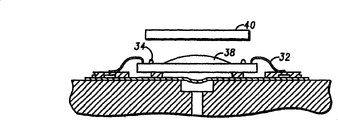
See figures.1.and.2, Fig. 1 is the enlarged side view according to image sensor devices 10 of the present invention, and Fig. 2 is the amplification decomposition figure of sensor component 10.Sensor component 10 comprises metal QFN (four limit flat no-leads) lead frame 12.Because the little form factor of QFN lead frame, low profile (profile) and low assembly cost are so it is preferred.Lead frame 12 has central die attach flag 14 and has the outer pad area 16 of a plurality of pads 18.Fixed head also has the annular element 20 on every side that forms the joint lining.The height of annular element 20 approximates the thickness of lead frame 12 greatly on every side.
Annular element 20 interior low stress low modulus chip fixed adhesives 24 were fixed on the fixed head 14 of lead frame 12 around sensor IC (IC) 22 preferably utilized and is arranged in fixed head.IC 22 has first surface, and this first surface has effective coverage 26 (Fig. 2) and peripheral pads zone 28.Peripheral pads zone 28 comprises pad 30.The cmos sensor device of the preferably as well known to those skilled in the art and type that on market, obtains easily of IC 22.IC 22 has the thickness or the height of about 15 mils.IC 22 also comprises circuit and logic except comprising optical receiving region (effective coverage 26), for example A/D converter and DSP or be used to carry out the logic region of type operation of counting.A plurality of leads 32 are arrived each IC pad 30 and each corresponding leadframe pad 18 by wire-bonded, thereby IC 22 and lead frame 12 are electrically connected.Lead 32 can for example well known to a person skilled in the art that the combination of conducting metal or metal forms by the combination of any conducting metal or metal.Suitable joint lining generally comprises the conducting metal such as copper or gold, and can be thin wire (diameter is less than 50 μ m) or heavy gauge wire (diameter is greater than 50 μ m).In a preferred embodiment, lead 32 is the thin wires that formed by gold.
Term " wire-bonded (wirebonding) " generally is meant the interconnection via lead formation of chip and substrate.The most frequently used method that connects the line on the pad is by hot acoustic pressure weldering (thermosonic bonding) or ultra-sonic welded.Ultrasonic leading wire engage to use rub interface between lead and the pad of the combination of vibration and pressure, causes that local temperature raises, and impels the cross-border diffusion of molecule.Heat is also used in hot acoustic pressure weldering except using vibration, this has further promoted the migration of material.
On the first surface of IC 22, form a plurality of column-shaped projections 34.In a preferred embodiment, column-shaped projection 34 is by forming with lead 32 identical materials, and is for example golden.Column-shaped projection 34 highly is about 3 mils, and its position is near IC effective coverage 26.The capillary that use is used to carry out the wire bonder of wire-bonded forms column-shaped projection 34 on IC 22.That is, except the do not circulate shaping (loop formation) and the second welding forming step, the technology that forms column-shaped projection 34 is very similar to common hot ultrasonic gold goal welding procedure.More specifically, form the free air ball that breaks away from and it is captured in the capillary, then on the surface of IC 22, form first solder joint by electric flame.After forming first solder joint, discharge tail length, and the execution afterbody is cut apart (breaking away from first solder joint).Each column-shaped projection is repeated this processing.
(Fig. 2) is arranged on the IC effective coverage 26 with transparency cover 36, and is shelved on the column-shaped projection 34.In present preferred embodiment, lid 36 comprise the transparent compound that is arranged on the IC effective coverage 26 and on cover transparent compound 38 and be shelved on window 40 on the column-shaped projection 34.Like this, column-shaped projection 34 is as 40 support of window.Lid 36 allows light to pass and arrive on the IC effective coverage 26.Window 40 is non-reflective optical grade glass preferably, and thickness is about 15 to 16 mils.Window 40 can apply various materials with filter light as required.Transparent compound 38 can be the transparent epoxy resin of liquid form before solidifying.Transparent compound 38 can be deposited on the transducer effective coverage 26 by any distribution system.Then, window 40 is placed on transparent compound 38 top of (with column-shaped projection 34).Then carry out hot curing and handle to solidify and hardening epoxy resin, like this, epoxy resin just is fixed to window 40 on the IC effective coverage 26.
In order to finish device 10, on the periphery of lead frame 12, wire bonds and lid 36, form mold compound 42.Column-shaped projection 34 supports as precise height, and maintenance window 40 is in the position between IC 22 and the mold compound 42.About 40 mils of image sensor devices 10 whole heights.
Referring now to Fig. 3, Fig. 3 shows the enlarged side view of image sensor devices 44 according to another embodiment of the invention.Except the sensor IC 45 of sensor component 44 has the bigger inactive area, sensor component 44 is similar to sensor component 10 (Fig. 1).That is, the top surface of sensor IC 45 has effective optical receiving region, the inactive area that does not comprise photoelectric cell and peripheral pads zone.Arrange transparent compound 38 on the IC effective coverage, lid 46 has the size that only covers the effective coverage, and covers 46 and adhere to the effective coverage via transparent compound 38.In the inactive area of lead frame 12, lead 32, IC 45 with cover on 46 the periphery and form mold compound 48.Because mold compound 48 covers the inactive area of IC 45, so have only the effective coverage of IC 45 to be exposed under the light.Thereby if IC 45 comprises photosensitive memory cell, then such unit is not subjected to the influence of light by the shielding of mold compound 48.
It should be noted that sensor component 44 does not comprise column-shaped projection, although can comprise column-shaped projection if desired.It should be appreciated by those skilled in the art that does not have column-shaped projection 34 can form first embodiment (device 10) yet.
Referring now to Fig. 4 A-4E, Fig. 4 A-4E shows the amplification profile of the step of the sensor component 10 that forms Fig. 1 and Fig. 2.Metal QFN lead frame 12 shown in Fig. 4 A has central die attach flag 14 and has the outer pad area of a plurality of pads.Fixed head 14 has annular element 20 on every side, and annular element 20 forms the thickness that engages lining and approximate lead frame 12 highly greatly on every side.In fixed head 14 surrounding annular elements 20, arranged die attach material 24.That is, fixed head 14 has the central opening that is used to receive bonding paste of low modulus or die attach adhesives.Die attach material 24 is known type, and is dispensed in a conventional manner on the fixed head 14.Sensor IC (IC) 22 is fixed to fixed head 14 by die attach material 24.Lead frame 12 can be equipped with molded mask tape (mold masking tape).Discuss with reference to Fig. 1 and 2 as the front, IC 22 has first surface, and this first surface has effective coverage and peripheral pads zone.The peripheral pads zone comprises pad.
Be fixed to the fixed head 14 of lead frame 12 at IC 22 after, assembly is transferred to segmentation and solidifies heating module 50, and the latter has vacuum hole 52.Shown in Fig. 4 B, assembly is positioned on the heating module 50, make fixed head 14 on hole 52.Apply vacuum power, make described band and die attach material 24 collapse in the vacuum hole.The action of subsiding is to be controlled by the size in the size of the vacuum power that applies and hole 52.Almost simultaneously, die attach material 24 is solidified.After finishing cure cycle, formed the projection 54 that stretches out from die attach layer.Projection 54 normally soft with plastic.As following further discussion, projection 54 is used for the altimetric compensation during the molded step.
With reference to Fig. 4 C, assembly moves to traditional wire bonder.Wire bonder comprises the heating module 56 with hole 58, and the size in hole 58 is bigger and allow assembly stably to place on the heating module 56 than projection 54.Carry out wire-bonded in a conventional manner, each IC pad and each corresponding leadframe pad are electrically connected to utilize many leads.And, utilize wire bonder capillary 60 on the first surface of IC 22, to form column-shaped projection 34.As discussed earlier, column-shaped projection 34 is by forming with lead 32 identical materials, that is, and and gold.In addition, the formation of column-shaped projection 34 does not need capillary 60 is made amendment.
With reference to Fig. 4 D, transparent compound or gel 38 are dispensed on the effective coverage 26 of sensor IC 22.The joint lining thickness of transparent compound 38 is by the height decision of column-shaped projection 34.According to the present invention, the height of column-shaped projection 34 is approximately 3 mils.Then, place window 40 on IC effective coverage 26, make window 40 be shelved on the column-shaped projection 34, window 40 is glass preferably.Transparent compound 38 is attached on the IC effective coverage 26 window 40, but window 40 is spaced apart by column-shaped projection 34 with IC 22.Total component thickness is controlled in very accurate tolerance.For example, the general height change of lead frame 12, IC 22, column-shaped projection 34 and window 40 is approximately+/-1.5 mils.Window 40 and transparent compound 38 allow light to pass and arrive on the IC effective coverage 26.
At last, shown in Fig. 4 E, on the periphery of lead frame 12, wire bonds and lid 40, form top mold compound (compound 42 among Fig. 1).Mold cavity depth A equals IC 22 and adds the thickness that cylindricality projection 34 adds window 40.The height of projection 54 equals total margin of tolerance of IC22, column-shaped projection 34 and window 40, is approximately 3 mils.Form after the mold compound on the periphery of lead frame 12, wire bonds and window 40, projection 54 subsides and is used to keep the power that window 40 contacts with molding cavity 62 with generation.That is, when assembly was enclosed in the mould, glass window 40 contacted with top molding cavity 62 by the very little power that subsiding of projection 54 produces.Because window leans against on the molding cavity 62, so the amount of resin of oozing out is restricted.Any a spot of resin that is seeped into glass surface can be cleaned by water spray subsequently and remove.In addition, even do not use boundary belt, also can avoid potential surface tear with the very little contact force of glass window 40 is also feasible.If form a plurality of devices simultaneously, then they form device shown in Figure 1 10 together.The height of the device of finishing is less than about 40 mils.
Here for example the purpose of illustration and description provided the explanation of the preferred embodiments of the present invention, but this explanation is not limit, neither limit the invention to disclosed form.It should be appreciated by those skilled in the art that and not depart from very wide inventive concept of the present invention and the foregoing description is made change.Thereby, should be appreciated that to the invention is not restricted to disclosed concrete form, but covered by the design of the present invention of claim definition and the modification in the scope.

Claims (12)

1. image sensor devices comprises:
Four limit flat no-lead type lead frames, this lead frame have central die attach flag and have the outer pad area of a plurality of pads;
Be fixed to the sensor IC on the described fixed head, described integrated circuit has first surface, and this first surface has effective coverage and peripheral pads zone, and described peripheral pads zone comprises pad;
A plurality of leads, it is arrived described each integrated circuit pad and corresponding described each leadframe pad by wire-bonded, thereby described integrated circuit and described lead frame are electrically connected;
A plurality of conducting metal column-shaped projections on the described first surface of described integrated circuit;
Transparency cover, it is set on the described integrated circuit effective coverage and is shelved on the described column-shaped projection, and described lid allows light to pass and arrive described integrated circuit effective coverage; With
Mold compound, it is formed on the periphery of described lead frame, wire bonds and described lid.
2. image sensor devices as claimed in claim 1, wherein said fixed head has annular element on every side, and annular element forms the joint lining of the thickness that approximates described lead frame highly greatly on every side.
3. image sensor devices as claimed in claim 2, wherein said integrated circuit is by being arranged in around the described fixed head low modulus adhesive in the annular element to described fixed head.
4. image sensor devices as claimed in claim 1, wherein said column-shaped projection is formed by gold.
5. image sensor devices as claimed in claim 4, the height of wherein said column-shaped projection is about 3 mils.
6. image sensor devices as claimed in claim 4, wherein said lead is formed by gold.
7. image sensor devices as claimed in claim 1 also comprises the transparent compound that is arranged between described integrated circuit effective coverage and the described lid.
8. image sensor devices as claimed in claim 7, wherein said lid is formed by glass.
9. image sensor devices as claimed in claim 1, wherein said column-shaped projection are formed on the described integrated circuit effective coverage.
10. image sensor devices as claimed in claim 1, the height of wherein said device is about 40 mils.
11. an image sensor devices comprises:
Four limit flat no-lead type lead frames, it has central die attach flag and has the outer pad area of a plurality of pads;
Be fixed to the sensor IC of described fixed head, described integrated circuit has first surface, and this first surface has effective coverage, inactive area and peripheral pads zone, and described peripheral pads zone comprises pad;
A plurality of leads, it is arrived described each integrated circuit pad and corresponding described each leadframe pad by wire-bonded, thereby described integrated circuit and described lead frame are electrically connected;
Be formed on a plurality of conducting metal column-shaped projections on the described first surface of described integrated circuit;
Be arranged in the transparent compound on the described integrated circuit effective coverage;
Transparent glass cover, it is arranged on the described transparent compound on the described integrated circuit effective coverage, and wherein light can pass described lid and described transparent compound arrives described integrated circuit effective coverage; With
Mold compound, it is formed on the periphery of described lead frame, wire bonds, leads of IC junction point, integrated circuit inactive area and described lid.
12. a method of making image sensor devices comprises the steps:
Four limit flat no-lead type lead frames are provided, it has central die attach flag and has the outer pad area of a plurality of pads, wherein said fixed head has annular element on every side, and annular element forms the joint lining of the thickness that approximates described lead frame highly greatly on every side;
The above arranges die attach material in the annular element on every side at described fixed head;
Utilize described die attach material that sensor IC is fixed on the described fixed head, described integrated circuit has first surface, and this first surface has effective coverage and peripheral pads zone, and described peripheral pads zone comprises pad;
Utilize a plurality of leads described each integrated circuit pad and corresponding described each leadframe pad to be electrically connected by wire-bonded;
On the described first surface of described integrated circuit, form a plurality of column-shaped projections;
Place transparency cover on described integrated circuit effective coverage, make described lid be shelved on the described column-shaped projection, wherein light can pass described lid and arrive described integrated circuit effective coverage; And
On the periphery of described lead frame, wire bonds and described lid, form mold compound.
CNB038246333A 2002-10-29 2003-09-30 Optical sensor package Expired - Fee Related CN100452441C (en)

Applications Claiming Priority (2)

Application Number Priority Date Filing Date Title
US10/282,537 2002-10-29
US10/282,537 US6667543B1 (en) 2002-10-29 2002-10-29 Optical sensor package

Publications (2)

Publication Number Publication Date
CN1692501A CN1692501A (en) 2005-11-02
CN100452441C true CN100452441C (en) 2009-01-14

Family

ID=29735714

Family Applications (1)

Application Number Title Priority Date Filing Date
CNB038246333A Expired - Fee Related CN100452441C (en) 2002-10-29 2003-09-30 Optical sensor package

Country Status (7)

Country Link
US (2) US6667543B1 (en)
JP (1) JP4705784B2 (en)
KR (1) KR101031394B1 (en)
CN (1) CN100452441C (en)
AU (1) AU2003275308A1 (en)
TW (1) TWI233685B (en)
WO (1) WO2004040660A1 (en)

Families Citing this family (63)

* Cited by examiner, † Cited by third party
Publication number Priority date Publication date Assignee Title
US7002241B1 (en) 2003-02-12 2006-02-21 National Semiconductor Corporation Packaging of semiconductor device with a non-opaque cover
US20060003483A1 (en) * 2003-07-07 2006-01-05 Wolff Larry L Optoelectronic packaging with embedded window
US20050009239A1 (en) * 2003-07-07 2005-01-13 Wolff Larry Lee Optoelectronic packaging with embedded window
US6995462B2 (en) 2003-09-17 2006-02-07 Micron Technology, Inc. Image sensor packages
US7138707B1 (en) * 2003-10-21 2006-11-21 Amkor Technology, Inc. Semiconductor package including leads and conductive posts for providing increased functionality
US6905910B1 (en) * 2004-01-06 2005-06-14 Freescale Semiconductor, Inc. Method of packaging an optical sensor
US7098529B1 (en) * 2004-01-07 2006-08-29 Credence Systems Corporation System and method for packaging a semiconductor device
KR100673950B1 (en) * 2004-02-20 2007-01-24 삼성테크윈 주식회사 Image sensor module and camera module package therewith
US7215018B2 (en) 2004-04-13 2007-05-08 Vertical Circuits, Inc. Stacked die BGA or LGA component assembly
US7705432B2 (en) 2004-04-13 2010-04-27 Vertical Circuits, Inc. Three dimensional six surface conformal die coating
JP4055762B2 (en) * 2004-05-25 2008-03-05 セイコーエプソン株式会社 Manufacturing method of electro-optical device
US20050266592A1 (en) * 2004-05-28 2005-12-01 Intersil Americas, Inc. Method of fabricating an encapsulated chip and chip produced thereby
US20050266602A1 (en) * 2004-05-28 2005-12-01 Intersil Americas, Inc. Encapsulated chip and method of fabrication thereof
TWI333249B (en) * 2004-08-24 2010-11-11 Himax Tech Inc Sensor package
US20060197201A1 (en) * 2005-02-23 2006-09-07 Hsin Chung H Image sensor structure
TW200707768A (en) * 2005-08-15 2007-02-16 Silicon Touch Tech Inc Sensing apparatus capable of easily selecting the light-sensing curve
US7897920B2 (en) * 2005-09-21 2011-03-01 Analog Devices, Inc. Radiation sensor device and method
TWI285417B (en) * 2005-10-17 2007-08-11 Taiwan Electronic Packaging Co Image chip package structure and packaging method thereof
CN101340884A (en) 2005-10-19 2009-01-07 曼尼·马纳舍·辛格尔 Methods for the treatment of hyperhidrosis
JP4382030B2 (en) * 2005-11-15 2009-12-09 富士通マイクロエレクトロニクス株式会社 Semiconductor device and manufacturing method thereof
JP4779614B2 (en) * 2005-12-08 2011-09-28 ヤマハ株式会社 Semiconductor device
WO2008082565A1 (en) * 2006-12-29 2008-07-10 Tessera, Inc. Microelectronic devices and methods of manufacturing such devices
US8723332B2 (en) * 2007-06-11 2014-05-13 Invensas Corporation Electrically interconnected stacked die assemblies
US7923349B2 (en) * 2007-06-19 2011-04-12 Vertical Circuits, Inc. Wafer level surface passivation of stackable integrated circuit chips
SG149724A1 (en) 2007-07-24 2009-02-27 Micron Technology Inc Semicoductor dies with recesses, associated leadframes, and associated systems and methods
SG149725A1 (en) * 2007-07-24 2009-02-27 Micron Technology Inc Thin semiconductor die packages and associated systems and methods
US8704379B2 (en) * 2007-09-10 2014-04-22 Invensas Corporation Semiconductor die mount by conformal die coating
US7911018B2 (en) * 2007-10-30 2011-03-22 Panasonic Corporation Optical device and method of manufacturing the same
JP2009124515A (en) * 2007-11-15 2009-06-04 Sharp Corp Imaging module and its manufacturing method, and electronic information device
KR101554761B1 (en) 2008-03-12 2015-09-21 인벤사스 코포레이션 Support mounted electrically interconnected die assembly
US9153517B2 (en) 2008-05-20 2015-10-06 Invensas Corporation Electrical connector between die pad and z-interconnect for stacked die assemblies
US7863159B2 (en) * 2008-06-19 2011-01-04 Vertical Circuits, Inc. Semiconductor die separation method
US8415203B2 (en) * 2008-09-29 2013-04-09 Freescale Semiconductor, Inc. Method of forming a semiconductor package including two devices
US7820485B2 (en) * 2008-09-29 2010-10-26 Freescale Semiconductor, Inc. Method of forming a package with exposed component surfaces
CN101740528B (en) * 2008-11-12 2011-12-28 力成科技股份有限公司 Radiating-enhanced outer pin-free semiconductor packaging structure and combination thereof
JP2010166021A (en) * 2008-12-18 2010-07-29 Panasonic Corp Semiconductor device, and manufacturing method thereof
JP5963671B2 (en) * 2009-06-26 2016-08-03 インヴェンサス・コーポレーション Electrical interconnection for stacked dies in zigzag configuration
US9147583B2 (en) 2009-10-27 2015-09-29 Invensas Corporation Selective die electrical insulation by additive process
TWI544604B (en) 2009-11-04 2016-08-01 英維瑟斯公司 Stacked die assembly having reduced stress electrical interconnects
US8492720B2 (en) 2010-06-08 2013-07-23 Avago Technologies General Ip (Singapore) Pte. Ltd. Small low-profile optical proximity sensor
US8742350B2 (en) 2010-06-08 2014-06-03 Avago Technologies General Ip (Singapore) Pte. Ltd. Proximity sensor
US8618620B2 (en) 2010-07-13 2013-12-31 Infineon Technologies Ag Pressure sensor package systems and methods
US8743207B2 (en) 2010-07-27 2014-06-03 Flir Systems Inc. Infrared camera architecture systems and methods
US20140175628A1 (en) * 2012-12-21 2014-06-26 Hua Pan Copper wire bonding structure in semiconductor device and fabrication method thereof
WO2014105989A1 (en) 2012-12-31 2014-07-03 Flir Systems, Inc. Wafer level packaging of microbolometer vacuum package assemblies
US9159852B2 (en) 2013-03-15 2015-10-13 Taiwan Semiconductor Manufacturing Company, Ltd. Image sensor device and method
US9368423B2 (en) 2013-06-28 2016-06-14 STATS ChipPAC Pte. Ltd. Semiconductor device and method of using substrate with conductive posts and protective layers to form embedded sensor die package
CN103996687A (en) * 2014-06-12 2014-08-20 中国电子科技集团公司第四十四研究所 Local-thinned backside illuminated type image sensor structure and packaging process thereof
US9871019B2 (en) 2015-07-17 2018-01-16 Invensas Corporation Flipped die stack assemblies with leadframe interconnects
US9490195B1 (en) 2015-07-17 2016-11-08 Invensas Corporation Wafer-level flipped die stacks with leadframes or metal foil interconnects
US9825002B2 (en) 2015-07-17 2017-11-21 Invensas Corporation Flipped die stack
WO2017049318A1 (en) 2015-09-18 2017-03-23 Synaptics Incorporated Optical fingerprint sensor package
US9508691B1 (en) 2015-12-16 2016-11-29 Invensas Corporation Flipped die stacks with multiple rows of leadframe interconnects
US10566310B2 (en) 2016-04-11 2020-02-18 Invensas Corporation Microelectronic packages having stacked die and wire bond interconnects
US9595511B1 (en) 2016-05-12 2017-03-14 Invensas Corporation Microelectronic packages and assemblies with improved flyby signaling operation
US9728524B1 (en) 2016-06-30 2017-08-08 Invensas Corporation Enhanced density assembly having microelectronic packages mounted at substantial angle to board
IT201700030588A1 (en) 2017-03-20 2018-09-20 Federica Livieri "COMPOSITION FOR USE IN THE TREATMENT OF HYPERIDROSIS PREPARING TO THE CUTANEOUS MYCOSIS OF THE FOOT"
EP3396329A1 (en) * 2017-04-28 2018-10-31 Sensirion AG Sensor package
US10177074B1 (en) 2017-10-04 2019-01-08 Semiconductor Components Industries, Llc Flexible semiconductor package
CN109346415B (en) * 2018-09-20 2020-04-28 江苏长电科技股份有限公司 Packaging method and packaging equipment for selectively packaging structure
CN111584529A (en) * 2020-05-18 2020-08-25 甬矽电子(宁波)股份有限公司 Sensor packaging structure and packaging method
US11747273B2 (en) * 2020-09-28 2023-09-05 Asahi Kasei Microdevices Corporation Gas sensor
US20220173256A1 (en) * 2020-12-02 2022-06-02 Texas Instruments Incorporated Optical sensor packages with glass members

Citations (4)

* Cited by examiner, † Cited by third party
Publication number Priority date Publication date Assignee Title
JPS5940566A (en) * 1982-08-30 1984-03-06 Canon Inc Manufacture of color solid-state image pick-up device
JPS61207062A (en) * 1985-03-12 1986-09-13 Seiko Epson Corp Solid-state image pickup device
JPS6269674A (en) * 1985-09-24 1987-03-30 Mitsubishi Electric Corp Solid-state image pickup device and manufacture of the same
US4957882A (en) * 1988-11-25 1990-09-18 Mitsubishi Denki Kabushiki Kaisha Method for manufacturing semiconductor device

Family Cites Families (17)

* Cited by examiner, † Cited by third party
Publication number Priority date Publication date Assignee Title
JPH0813107B2 (en) * 1986-09-05 1996-02-07 オリンパス光学工業株式会社 Solid-state imaging device
JPH0724287B2 (en) * 1987-02-12 1995-03-15 三菱電機株式会社 Semiconductor device having light transmitting window and method of manufacturing the same
US5264393A (en) * 1988-11-25 1993-11-23 Fuji Photo Film Co., Ltd. Solid state image pickup device and method of manufacturing the same
JPH0378617A (en) * 1989-08-22 1991-04-03 K G S Kk Position sensor
JPH065828A (en) * 1992-06-16 1994-01-14 Sony Corp Extra-small ccd module
JPH1197656A (en) 1997-09-22 1999-04-09 Fuji Electric Co Ltd Semiconductor photosensor device
WO2001015237A1 (en) 1999-08-20 2001-03-01 Amkor Technology, Inc. Chip-sized optical sensor package
US6266197B1 (en) 1999-12-08 2001-07-24 Amkor Technology, Inc. Molded window array for image sensor packages
JP2001203913A (en) * 2000-01-21 2001-07-27 Sony Corp Image pickup device, camera module, and camera system
US6384472B1 (en) 2000-03-24 2002-05-07 Siliconware Precision Industries Co., Ltd Leadless image sensor package structure and method for making the same
US6492699B1 (en) * 2000-05-22 2002-12-10 Amkor Technology, Inc. Image sensor package having sealed cavity over active area
JP3725012B2 (en) * 2000-08-17 2005-12-07 シャープ株式会社 Manufacturing method of lens-integrated solid-state imaging device
US6342406B1 (en) 2000-11-15 2002-01-29 Amkor Technology, Inc. Flip chip on glass image sensor package fabrication method
JP3078617U (en) * 2000-12-27 2001-07-10 汎太半導體股▲ふん▼有限公司 Image IC packaging structure
JP4637380B2 (en) * 2001-02-08 2011-02-23 ルネサスエレクトロニクス株式会社 Semiconductor device
US6661083B2 (en) * 2001-02-27 2003-12-09 Chippac, Inc Plastic semiconductor package
JP2002270803A (en) * 2001-03-14 2002-09-20 Ricoh Co Ltd Solid-state imaging device, image reading unit, and image forming device

Patent Citations (4)

* Cited by examiner, † Cited by third party
Publication number Priority date Publication date Assignee Title
JPS5940566A (en) * 1982-08-30 1984-03-06 Canon Inc Manufacture of color solid-state image pick-up device
JPS61207062A (en) * 1985-03-12 1986-09-13 Seiko Epson Corp Solid-state image pickup device
JPS6269674A (en) * 1985-09-24 1987-03-30 Mitsubishi Electric Corp Solid-state image pickup device and manufacture of the same
US4957882A (en) * 1988-11-25 1990-09-18 Mitsubishi Denki Kabushiki Kaisha Method for manufacturing semiconductor device

Also Published As

Publication number Publication date
TWI233685B (en) 2005-06-01
KR20050071637A (en) 2005-07-07
US20040080029A1 (en) 2004-04-29
CN1692501A (en) 2005-11-02
WO2004040660A1 (en) 2004-05-13
KR101031394B1 (en) 2011-04-26
US6667543B1 (en) 2003-12-23
JP2006505126A (en) 2006-02-09
TW200414476A (en) 2004-08-01
AU2003275308A1 (en) 2004-05-25
JP4705784B2 (en) 2011-06-22
US6958261B2 (en) 2005-10-25

Similar Documents

Publication Publication Date Title
CN100452441C (en) Optical sensor package
US6770163B1 (en) Mold and method for encapsulation of electronic device
US6384472B1 (en) Leadless image sensor package structure and method for making the same
KR100526844B1 (en) semiconductor package and its manufacturing method
US6767753B2 (en) Image sensor of a quad flat package
JP2843464B2 (en) Solid-state imaging device
JPH08306899A (en) Package for solid-state image pickup element and its preparation
JPH07221278A (en) Solid-state image pickup element and its preparation
JP2002118207A (en) Semiconductor package and method for manufacturing the same
US6372551B1 (en) Method of manufacturing an image-sensor integrated circuit package without resin flash on lead frame and with increased wire bondability
US7002257B2 (en) Optical component package and packaging including an optical component horizontally attached to a substrate
JP2003332542A (en) Semiconductor device and method of manufacturing the same
CN100495689C (en) Method of packaging an optical sensor and image sensor device
KR20070015014A (en) Method of making a stacked die package
KR940001333A (en) Resin-sealed solid state image pickup device package and manufacturing method thereof
US6864564B2 (en) Flash-preventing semiconductor package
US20030038358A1 (en) Semiconductor package without outer leads
US20040036151A1 (en) Double leadframe-based packaging structure and manufacturing process thereof
JPH0745655A (en) Sealing structure of semiconductor element
US5960261A (en) Method for manufacturing semiconductor package
KR100455698B1 (en) chip size package and its manufacturing method
JPH07169780A (en) Col semiconductor device and its lead frame
JPH07105408B2 (en) Method for manufacturing resin-encapsulated semiconductor device and molding die
KR0135889Y1 (en) Complex-type semiconductor package
KR19990058160A (en) BG package and manufacturing method thereof

Legal Events

Date Code Title Description
C06 Publication
PB01 Publication
C10 Entry into substantive examination
SE01 Entry into force of request for substantive examination
C14 Grant of patent or utility model
GR01 Patent grant
ASS Succession or assignment of patent right

Owner name: TANGCHUNG CO., LTD.

Free format text: FORMER OWNER: FISICAL SEMICONDUCTOR INC.

Effective date: 20100729

C41 Transfer of patent application or patent right or utility model
COR Change of bibliographic data

Free format text: CORRECT: ADDRESS; FROM: TEXAS, USA TO: DELAWARE STATE, USA

TR01 Transfer of patent right

Effective date of registration: 20100729

Address after: Delaware

Patentee after: Tong song Co.,Ltd.

Address before: Texas in the United States

Patentee before: FREESCALE SEMICONDUCTOR, Inc.

CF01 Termination of patent right due to non-payment of annual fee

Granted publication date: 20090114

CF01 Termination of patent right due to non-payment of annual fee