CN100371963C - Display - Google Patents
Display Download PDFInfo
- Publication number
- CN100371963C CN100371963C CNB2004100916781A CN200410091678A CN100371963C CN 100371963 C CN100371963 C CN 100371963C CN B2004100916781 A CNB2004100916781 A CN B2004100916781A CN 200410091678 A CN200410091678 A CN 200410091678A CN 100371963 C CN100371963 C CN 100371963C
- Authority
- CN
- China
- Prior art keywords
- signal
- aforementioned
- supply circuit
- circuit parts
- auxiliary capacitance
- Prior art date
- Legal status (The legal status is an assumption and is not a legal conclusion. Google has not performed a legal analysis and makes no representation as to the accuracy of the status listed.)
- Expired - Fee Related
Links
Images


Classifications
-
- G—PHYSICS
- G09—EDUCATION; CRYPTOGRAPHY; DISPLAY; ADVERTISING; SEALS
- G09G—ARRANGEMENTS OR CIRCUITS FOR CONTROL OF INDICATING DEVICES USING STATIC MEANS TO PRESENT VARIABLE INFORMATION
- G09G3/00—Control arrangements or circuits, of interest only in connection with visual indicators other than cathode-ray tubes
- G09G3/20—Control arrangements or circuits, of interest only in connection with visual indicators other than cathode-ray tubes for presentation of an assembly of a number of characters, e.g. a page, by composing the assembly by combination of individual elements arranged in a matrix no fixed position being assigned to or needed to be assigned to the individual characters or partial characters
- G09G3/34—Control arrangements or circuits, of interest only in connection with visual indicators other than cathode-ray tubes for presentation of an assembly of a number of characters, e.g. a page, by composing the assembly by combination of individual elements arranged in a matrix no fixed position being assigned to or needed to be assigned to the individual characters or partial characters by control of light from an independent source
- G09G3/36—Control arrangements or circuits, of interest only in connection with visual indicators other than cathode-ray tubes for presentation of an assembly of a number of characters, e.g. a page, by composing the assembly by combination of individual elements arranged in a matrix no fixed position being assigned to or needed to be assigned to the individual characters or partial characters by control of light from an independent source using liquid crystals
- G09G3/3611—Control of matrices with row and column drivers
- G09G3/3648—Control of matrices with row and column drivers using an active matrix
- G09G3/3655—Details of drivers for counter electrodes, e.g. common electrodes for pixel capacitors or supplementary storage capacitors
-
- G—PHYSICS
- G09—EDUCATION; CRYPTOGRAPHY; DISPLAY; ADVERTISING; SEALS
- G09G—ARRANGEMENTS OR CIRCUITS FOR CONTROL OF INDICATING DEVICES USING STATIC MEANS TO PRESENT VARIABLE INFORMATION
- G09G3/00—Control arrangements or circuits, of interest only in connection with visual indicators other than cathode-ray tubes
- G09G3/20—Control arrangements or circuits, of interest only in connection with visual indicators other than cathode-ray tubes for presentation of an assembly of a number of characters, e.g. a page, by composing the assembly by combination of individual elements arranged in a matrix no fixed position being assigned to or needed to be assigned to the individual characters or partial characters
-
- G—PHYSICS
- G09—EDUCATION; CRYPTOGRAPHY; DISPLAY; ADVERTISING; SEALS
- G09G—ARRANGEMENTS OR CIRCUITS FOR CONTROL OF INDICATING DEVICES USING STATIC MEANS TO PRESENT VARIABLE INFORMATION
- G09G2300/00—Aspects of the constitution of display devices
- G09G2300/08—Active matrix structure, i.e. with use of active elements, inclusive of non-linear two terminal elements, in the pixels together with light emitting or modulating elements
- G09G2300/0876—Supplementary capacities in pixels having special driving circuits and electrodes instead of being connected to common electrode or ground; Use of additional capacitively coupled compensation electrodes
-
- G—PHYSICS
- G09—EDUCATION; CRYPTOGRAPHY; DISPLAY; ADVERTISING; SEALS
- G09G—ARRANGEMENTS OR CIRCUITS FOR CONTROL OF INDICATING DEVICES USING STATIC MEANS TO PRESENT VARIABLE INFORMATION
- G09G2320/00—Control of display operating conditions
- G09G2320/02—Improving the quality of display appearance
- G09G2320/0219—Reducing feedthrough effects in active matrix panels, i.e. voltage changes on the scan electrode influencing the pixel voltage due to capacitive coupling
-
- G—PHYSICS
- G09—EDUCATION; CRYPTOGRAPHY; DISPLAY; ADVERTISING; SEALS
- G09G—ARRANGEMENTS OR CIRCUITS FOR CONTROL OF INDICATING DEVICES USING STATIC MEANS TO PRESENT VARIABLE INFORMATION
- G09G2320/00—Control of display operating conditions
- G09G2320/02—Improving the quality of display appearance
- G09G2320/0247—Flicker reduction other than flicker reduction circuits used for single beam cathode-ray tubes
-
- G—PHYSICS
- G09—EDUCATION; CRYPTOGRAPHY; DISPLAY; ADVERTISING; SEALS
- G09G—ARRANGEMENTS OR CIRCUITS FOR CONTROL OF INDICATING DEVICES USING STATIC MEANS TO PRESENT VARIABLE INFORMATION
- G09G2330/00—Aspects of power supply; Aspects of display protection and defect management
- G09G2330/02—Details of power systems and of start or stop of display operation
- G09G2330/021—Power management, e.g. power saving
-
- G—PHYSICS
- G09—EDUCATION; CRYPTOGRAPHY; DISPLAY; ADVERTISING; SEALS
- G09G—ARRANGEMENTS OR CIRCUITS FOR CONTROL OF INDICATING DEVICES USING STATIC MEANS TO PRESENT VARIABLE INFORMATION
- G09G3/00—Control arrangements or circuits, of interest only in connection with visual indicators other than cathode-ray tubes
- G09G3/20—Control arrangements or circuits, of interest only in connection with visual indicators other than cathode-ray tubes for presentation of an assembly of a number of characters, e.g. a page, by composing the assembly by combination of individual elements arranged in a matrix no fixed position being assigned to or needed to be assigned to the individual characters or partial characters
- G09G3/34—Control arrangements or circuits, of interest only in connection with visual indicators other than cathode-ray tubes for presentation of an assembly of a number of characters, e.g. a page, by composing the assembly by combination of individual elements arranged in a matrix no fixed position being assigned to or needed to be assigned to the individual characters or partial characters by control of light from an independent source
- G09G3/36—Control arrangements or circuits, of interest only in connection with visual indicators other than cathode-ray tubes for presentation of an assembly of a number of characters, e.g. a page, by composing the assembly by combination of individual elements arranged in a matrix no fixed position being assigned to or needed to be assigned to the individual characters or partial characters by control of light from an independent source using liquid crystals
- G09G3/3611—Control of matrices with row and column drivers
- G09G3/3614—Control of polarity reversal in general
Landscapes
- Engineering & Computer Science (AREA)
- Physics & Mathematics (AREA)
- Computer Hardware Design (AREA)
- General Physics & Mathematics (AREA)
- Theoretical Computer Science (AREA)
- Chemical & Material Sciences (AREA)
- Crystallography & Structural Chemistry (AREA)
- Power Engineering (AREA)
- Liquid Crystal Display Device Control (AREA)
- Liquid Crystal (AREA)
- Control Of Indicators Other Than Cathode Ray Tubes (AREA)
- Electroluminescent Light Sources (AREA)
Abstract
A display device capable of making a flicker hard to be visually recognized and reducing the power consumption is improved. The display device is comprised of pixel parts (3a) and (3b) each includes an auxiliary capacitance (33) having an electrode (36) connected to a pixel electrode (34) and an electrode (37), auxiliary capacitance lines (SC1-1) to (SC1-4) and (SC2-1) to (SC2-4) connected to the electrodes (37) of the auxiliary capacitances (33) of the pixel parts (3a) and (3b) respectively, and a signal supply circuit (7) includes signal supply circuit parts (7a) to (7d) for supplying either one of H side signal (VSCH) and L side signal (VSCL) and another one of the same to the auxiliary capacitance lines (SC1-1) to (SC1-4) of the pixel part (3a) and the auxiliary capacitance lines (SC2-1) to (SC2-4) of the pixel part (3b) respectively.
Description
Technical field
The present invention relates to display device, particularly relate to display device with pixel component.
Background technology
In existing display device, people have known and have possessed the liquid crystal indicator that the pixel component that comprises liquid crystal is arranged.Existing liquid crystal indicator comprises: the formation that the liquid crystal layer of pixel component is clipped in the middle by pixel electrode and counter electrode (common electrode).In addition, existing liquid crystal indicator changes the arrangement of liquid crystal molecule by the voltage (picture signal) that control puts on the pixel electrode of pixel component, and makes the image of corresponding image signals be shown in display unit.
In above-mentioned liquid crystal indicator, when for a long time DC voltage being put on the liquid crystal (pixel electrode) of pixel component, will produce so-called afterimage phenomena.Therefore, when driving liquid crystal indicator, the driving method that must use a kind of voltage (pixel voltage) that makes pixel electrode with the cycle of being scheduled to reverse with respect to the voltage of counter electrode.One example of the driving method of this liquid crystal indicator can exemplify a kind of direct drive method that DC voltage is put on counter electrode.In addition, the direct drive method is again because in each horizontal period, the line inversion driving method that makes pixel voltage and reverse with respect to the voltage of the counter electrode that is applied with DC voltage is known by people, and (reference example is as Suzuki 82 works " the LCD engineering is crossed the threshold ", Nikkan Kogyo Shimbun, on November 20th, 1998, the 101-103 page or leaf).A wherein so-called horizontal period is meant to be finished the time that writes picture signal in all pixel components that dispose along a gate line.
Oscillogram when Figure 14 drives liquid crystal indicator for using existing line inversion driving method.With reference to Figure 14, when using existing line inversion driving method to drive liquid crystal indicator,, make pixel voltage (picture signal) VIDEO with respect to the voltage COM of counter electrode and reverse in each horizontal period.In addition, in each pixel component A to F, pixel voltage (picture signal) VIDEO is changed according to image to display.
Yet, when using existing line inversion driving method shown in Figure 14 to carry out the driving of liquid crystal indicator,, have the problem of discovering flicker (flicker) easily if will reduce power consumption by driving with low frequency.Particularly, when carrying out the driving of liquid crystal indicator with low frequency, because of the time that keeps pixel voltage elongated, so the variation of pixel voltage can become big and this elongated corresponding deal.Like this, when the variation of pixel voltage became big, the brightness meeting of the light by pixel component A to F departed from desirable brightness, and produced flicker.In addition, in existing line inversion driving method, take place, discovered so the situation of flicker is very easy because of above-mentioned flicker is wire.
Therefore, prior art has disclosed a kind of liquid crystal indicator, and it utilizes in each pixel adjacent components A to F, the some inversion driving method that pixel voltage (picture signal) VIDEO is reversed with respect to the voltage COM of counter electrode.
Oscillogram when Figure 15 drives liquid crystal indicator for using existing some inversion driving method.With reference to Figure 15, when using existing some inversion driving method to drive liquid crystal indicator, the place that is different from existing line inversion driving method is at each pixel component A to F, make pixel voltage (picture signal) VIDEO, with respect to the voltage COM of counter electrode and reverse corresponding to the image that will show.When utilizing this existing some inversion driving method to carry out the driving of liquid crystal display,, discovered so the situation of flicker is difficult even, also take place because of this scintigram picture can not be wire because of driving with low frequency and causing flicker to produce.
Summary of the invention
Yet, in existing some inversion driving method shown in Figure 15, reverse with respect to the voltage COM of the counter electrode that is applied with DC voltage for making pixel voltage (picture signal) VIDEO, need have the picture signal of the double voltage of liquid crystal drive voltage.For example: in Figure 15, when liquid crystal drive voltage is made as V1, for making pixel voltage (picture signal) VIDEO all can obtain identical liquid crystal drive voltage V1 before and after reversing with respect to the voltage COM of counter electrode, must have the picture signal of the double voltage of liquid crystal drive voltage V1.Therefore, reduce power consumption, in the reduction of power consumption, still have its restriction even desire to drive liquid crystal indicator with low frequency.
For solving the above problems, the object of the present invention is to provide a kind ofly to be difficult for discovering flicker, and the display device that consumes of cpable of lowering power.
For achieving the above object, the display device according to a form of the present invention comprises: many drain lines and many gate lines of disposing in cross one another mode; First pixel component and second pixel component that comprise auxiliary capacitor respectively, this auxiliary capacitor have first electrode and second electrode that is connected with pixel electrode; First auxiliary capacitance line that is connected with second electrode of the aforementioned auxiliary capacitor of aforementioned first pixel component; Second auxiliary capacitance line that is connected with second electrode of the aforementioned auxiliary capacitor of aforementioned second pixel component; And the signal supply circuit that comprises a plurality of signal supply circuit parts, these signal supply circuit parts are supplied to first auxiliary capacitance line of first pixel component and second auxiliary capacitance line of second pixel component respectively in order to first signal that will have first voltage and the secondary signal with second voltage.
In the display device of above-mentioned form, by above-mentioned signal supply circuit is set, for example: when first voltage is that high level, second voltage are that the low level and first signal are when being supplied to first auxiliary capacitance line of first pixel component and second auxiliary capacitance line that secondary signal is supplied to second pixel component, because of first signal of high level is second electrode that is supplied to the auxiliary capacitor of first pixel component by first auxiliary capacitance line, therefore so that the voltage of the auxiliary capacitor of first pixel component rises to high level.In addition, low level secondary signal is second electrode that is supplied to the auxiliary capacitor of second pixel component by second auxiliary capacitance line, therefore gets so that the voltage of the auxiliary capacitor of second pixel component drops to low level.By this, finish after the writing of the picture signal of the high level of first pixel component, as long as first signal of high level is supplied to second electrode of the auxiliary capacitor of first pixel component, can make the voltage of the pixel electrode of first pixel component, be higher than and just finish picture signal and write fashionable state.In addition, finish after the writing of the low level picture signal of second pixel component, as long as low level secondary signal is supplied to second electrode of the auxiliary capacitor of second pixel component, the voltage of the pixel electrode of second pixel component is lower than just finish picture signal and writes fashionable state.Thus, owing to need not to increase the voltage of picture signal, can suppress to increase the increase of the power consumption that causes at an easy rate because of image signal voltage.As a result, the consumption of cpable of lowering power.In addition, in each pixel adjacent parts, when making the some inversion driving that pixel voltage (picture signal) reverses with respect to the voltage of common electrode, only need dispose first pixel component and second pixel component, can carry out an inversion driving easily by mode with adjacency.In addition, make pixel voltage (picture signal) and during the piece inversion driving of reversing in each of a plurality of pixel components with respect to the voltage of common electrode, by constituting a block (block) with a plurality of first pixel components, and constitute another block with a plurality of second pixel components, and dispose a block and another block in the mode of adjacency, can carry out the piece inversion driving easily.As mentioned above, by carrying out an inversion driving or piece inversion driving, be different from the line inversion driving that pixel voltage (picture signal) is reversed with respect to the voltage of common electrode, take place, be difficult for discovering so glimmer because flicker can not be wire.
In the display device of above-mentioned form, preferably each bar corresponding to many gate lines is provided with signal supply circuit parts respectively, and each signal supply circuit parts are supplied to first signal and secondary signal respectively first auxiliary capacitance line and second auxiliary capacitance line of pairing each bar gate line in regular turn.According to this formation, when each gate line disposes first pixel component and second pixel component, when picture signal is written into first pixel component of each gate line and second pixel component in regular turn, each signal supply circuit parts be can pass through, first auxiliary capacitance line and second auxiliary capacitance line in regular turn a side of first signal and secondary signal and the opposing party are supplied to easily corresponding to each gate line.
In the display device of above-mentioned form, preferably signal supply circuit parts are set respectively, and signal supply circuit parts are supplied to first signal and secondary signal first auxiliary capacitance line and second auxiliary capacitance line of pairing many gate lines respectively simultaneously corresponding to every many gate lines.By this formation, compared to the situation that disposes signal supply circuit parts corresponding to each bar of many gate lines, can reduce the quantity of signal supply circuit parts, therefore can when dwindling circuit scale, promote yield rate.
In the display device of above-mentioned form, preferably also possessing has: comprise the gate line drive circuit in order to first shift register that drives many gate lines in regular turn; And be provided with respectively with the gate line drive circuit that comprises first shift register, in order to drive second shift register of a plurality of signal supply circuit parts in regular turn.By this formation, can drive in regular turn by second shift register easily: with by the gate line drive circuit that comprises first shift register the corresponding signal supply circuit parts of gate line that drive in regular turn.
At this moment, preferred second shift register is driven with second pulse signal that has in order to two doubling times in cycle of first pulse signal that drives first shift register.By this formation, when respectively a side of first signal and secondary signal and the opposing party being supplied to simultaneously corresponding to first auxiliary capacitance line of two predetermined gate lines and second auxiliary capacitance line, the quantity that constitutes the shift-register circuit parts of second shift register can be lowered half for the quantity of the shift-register circuit parts that constitute first shift register, therefore, can when dwindling circuit scale, further promote yield rate.
In the display device of above-mentioned form, preferably also possessing has: comprise the gate line drive circuit in order to the shift register that drives many gate lines in regular turn, and a plurality of signal supply circuit parts are by the shift register institute driving in regular turn of gate line drive circuit.By this formation, owing to need not outside the shift register that drives many gate lines in regular turn, be provided with separately in order to drive the shift register of a plurality of signal supply circuit parts in regular turn, therefore, can when dwindling circuit scale, further promote yield rate.
At this moment, the shift register of preferred gate line drive circuit comprises a plurality of shift-register circuit parts, and the output signal of the later shift-register circuit parts of next section of this predetermined section of signal supply circuit unit response of predetermined section and export first signal and secondary signal.By this formation, because the output signal that the later shift-register circuit parts of next section of predetermined section are exported just is output after the output signal of output in order to the shift register of the gate line of driving predetermined section, therefore can be more easily after finishing picture signal to first pixel component that disposes along the gate line of predetermined section and second pixel component and writing, a side of first signal and secondary signal and the opposing party are supplied to first auxiliary capacitance line and second auxiliary capacitance line corresponding to the gate line of predetermined section respectively.
In the display device of above-mentioned form, preferred first pixel component and above-mentioned second pixel component dispose in the mode that adjoins each other.By this formation, can carry out easily making pixel voltage (picture signal) with respect to the voltage of common electrode and the some inversion driving of reversing at each pixel adjacent parts.
In the display device of above-mentioned form, preferred signals supply circuit parts are supplied to first auxiliary capacitance line and second auxiliary capacitance line respectively with first signal and secondary signal after finishing picture signal to all pixel components of disposing along at least one gate line and writing.By this formation, the pixel voltage of all pixel components that dispose along at least one gate line is higher or lower than just finish picture signal and writes fashionable state.
At this moment, preferred signals supply circuit parts each mode with mutual switching of (image duration) during finishing that picture signal to all pixel components writes is supplied to first auxiliary capacitance line and second auxiliary capacitance line respectively with first signal and secondary signal.By this formation, can be in each image duration, the image signal voltage of the pixel electrode by making the pixel electrode that writes first pixel component and second pixel component reverses with respect to the voltage of common electrode, and carries out an inversion driving or piece inversion driving easily.At this moment, also can suppress the generation of afterimage phenomena.
In the display device of above-mentioned form, preferred first pixel component and second pixel component dispose in the mode that adjoins each other, and the picture signal that is supplied to first electrode of first pixel component and second pixel component has the waveform of mutual counter-rotating.By this formation, can carry out an inversion driving easily.
In the display device of above-mentioned form, preferred only dispose in the mode that adjoins each other, and the signal that is supplied to a plurality of first pixel components that constitute first block and constitutes a plurality of second pixel components of second block has the waveform of mutual counter-rotating by a plurality of first pixel components first block that constitutes and second block that only constitutes by a plurality of second pixel components.By this formation, can carry out the piece inversion driving easily.
Description of drawings
Fig. 1 is the planimetric map according to the liquid crystal indicator of first embodiment of the invention.
Fig. 2 is the block scheme of the liquid crystal indicator of first embodiment shown in Figure 1.
Fig. 3 is the circuit diagram of signal supply circuit parts of the liquid crystal indicator of displayed map 1 and first embodiment shown in Figure 2.
Fig. 4 is the sequential chart in order to the action of V driver, signal supply circuit and the shift register of the liquid crystal indicator that first embodiment shown in Figure 2 is described.
Fig. 5 is the oscillogram in order to the action of the pixel component of the liquid crystal indicator that first embodiment shown in Figure 1 is described.
Fig. 6 is the oscillogram in order to the action of the pixel component of the liquid crystal indicator that first embodiment shown in Figure 1 is described.
Fig. 7 is the block scheme according to the liquid crystal indicator of second embodiment of the invention.
Fig. 8 is the circuit diagram of the signal supply circuit parts of the liquid crystal indicator of demonstration second embodiment shown in Figure 7.
Fig. 9 is the sequential chart in order to the action of V driver, signal supply circuit and the shift register of the liquid crystal indicator that second embodiment shown in Figure 7 is described.
Figure 10 is the block scheme according to the liquid crystal indicator of third embodiment of the invention.
Figure 11 is the sequential chart in order to the action of V driver, signal supply circuit and the shift register of the liquid crystal indicator that the 3rd embodiment shown in Figure 10 is described.
Figure 12 is the planimetric map according to the liquid crystal indicator of fourth embodiment of the invention.
Figure 13 is the block scheme of the liquid crystal indicator of the 4th embodiment shown in Figure 12.
Oscillogram when Figure 14 drives liquid crystal indicator for using existing line inversion driving method.
Oscillogram when Figure 15 drives liquid crystal indicator for using existing some inversion driving method.
Embodiment
Below in conjunction with the description of drawings specific embodiments of the invention.
Fig. 1 is the planimetric map according to the liquid crystal indicator of first embodiment of the invention, and Fig. 2 is the block scheme of the liquid crystal indicator of first embodiment shown in Figure 1.Fig. 3 is the circuit diagram of signal supply circuit parts of the liquid crystal indicator of displayed map 1 and first embodiment shown in Figure 2.
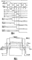
At first, in first embodiment, dispose display unit 2 on the substrate 1 with reference to Fig. 1.Dispose pixel component 3a and 3b in the display unit 2.In addition, in Fig. 1, be the simplification drawing, two drain line D1 that only show a gate lines G 1 and intersect with this gate lines G 1 and D2, and along the pixel component 3a and the 3b of gate lines G 1 configuration, dispose but be actually, and pixel component 3a and 3b are configured to rectangular in the mode that adjoins each other with many gate lines and many cross one another modes of drain line.In addition, pixel component 3a and 3b are respectively an example of " first pixel component " of the present invention and " second pixel component ".
In addition, the drain electrode of the n channel transistor 32 of pixel component 3a is connected to drain line D1, and the drain electrode of the n channel transistor 32 of pixel component 3b is connected to drain line D2.The source electrode of pixel component 3a and 3b is connected to pixel electrode 34 respectively.
In addition, an electrode 36 of the auxiliary capacitor 33 of pixel component 3a and 3b is connected to pixel electrode 34 respectively.Another electrode 37a of the auxiliary capacitor 33 of pixel component 3a is connected to auxiliary capacitance line SC1-1, and another electrode 37b of the auxiliary capacitor 33 of pixel component 3b then is connected to auxiliary capacitance line SC2-1.In addition, electrode 36 is an example of " first electrode " of the present invention, and electrode 37a and 37b are an example of " second electrode " of the present invention.In addition, auxiliary capacitance line SC1-1 is an example of " first auxiliary capacitance line " of the present invention, and auxiliary capacitance line SC2-1 then is an example of " second auxiliary capacitance line " of the present invention.
In addition, on substrate 1, dispose: in order to n channel transistor (H switch) 4a and the 4b that drives (scanning) drain line D1 and D2 and be not shown in three sections later drain lines among the figure; And H driver 5.In addition, be connected to image signal line VIDEO1, then be connected to image signal line VIDEO2 corresponding to the n channel transistor 4b of pixel component 3b (drain line D2) corresponding to the n channel transistor 4a of pixel component 3a (drain line D1).In addition, configuration on substrate 1: in order to gate lines G 1 that drives (scanning) first section and the V driver 6 that is not shown in second section later gate line among Fig. 1.In addition, V driver 6 is an example of " gate line drive circuit " of the present invention and " first shift register ".
In first embodiment, dispose signal supply circuit 7 and shift register 8 on the substrate 1.In addition, be connected to signal supply circuit 7 (signal supply circuit parts 7a) corresponding to the auxiliary capacitance line SC1-1 of pixel component 3a and corresponding to the auxiliary capacitance line SC2-1 of pixel component 3b.Signal supply circuit parts 7 had in each image duration, with the side of the signal VSCL of the signal VSCH of high-side and low level side and the function that an other side is supplied to auxiliary capacitance line SC1-1 and SC2-1 alternately.In addition, be meant a so-called image duration: to constituting all pixel component 3a and 3b of display unit 2, the time that writes of finishing picture element signal.In addition, shift register 8 has the function of drive signal supply circuit 7, makes the signal of signal supply circuit 7 be able in regular turn supplying with from a pair of auxiliary capacitance line SC1-1 that extends along first section gate lines G 1 and SC2-1 to a pair of auxiliary capacitance line (not being shown in the figure) that the gate line along terminal section extends.In addition, shift register 8 is an example of " second shift register " of the present invention.
In addition, the exterior arrangement at substrate 1 has drive IC.Positive level HVDD, negative level HVSS, activation signal STH and clock signal C KH system are supplied to H driver 5 by this drive IC 9.Positive level VVDD, negative level VVSS, activation signal STV, clock signal CKV and enable signal ENB then are supplied to V driver 6 by this drive IC 9.In addition, high level VSCH, low level VSCL and clock signal CKV SC are supplied to signal supply circuit 7 by drive IC 9.In addition, identical with the signal that is supplied to V driver 6 signal is supplied to shift register 8 by drive IC 9.
Below with reference to Fig. 2, illustrate that the inside of V driver 6, signal supply circuit 7 and shift register 8 constitutes.V driver 6 comprises shift-register circuit parts 61a to 61f.In addition, V driver 6 comprises the AND circuit block 62a to 62e with three input ends and an output terminal.
The output signal that is input as shift- register circuit parts 61a and 61b of the input end of AND circuit block 62a and enable signal ENB.And at the output signal that is input as shift- register circuit parts 61b and 61c and the enable signal ENB of the input end of AND circuit block 62b.By that analogy, AND circuit block 62c's is input as and interlace one section the output signal and the enable signal ENB of two sections shift-register circuit parts of AND circuit block.In addition, just export high level signal at AND circuit block 62a to 62e when three input signals are all high level, needing only one of them signal in three input signals is low level, i.e. the output low level signal.In addition, the output terminal of AND circuit block 62a to 62e is connected to gate lines G 1 respectively to G5.In addition, though do not show in the drawings, between AND circuit block and gate line, be connected with shift-register circuit.
In addition, signal supply circuit 7 comprises signal supply circuit parts 7a to 7d.In addition, signal supply circuit parts 7a to 7d is provided with in the mode that corresponds respectively to gate lines G 1 to G4.In addition, for simplifying drawing, do not show signal supply circuit parts among the figure corresponding to gate lines G 5.
In addition, the detailed circuit of relevant signal supply circuit parts 7a is formed as shown in Figure 3, and it is by phase inverter 71a to 71c; Time control phase inverter (clocked inverter) 72a and 72b; And switch 73a to 73d constitutes.In addition, switch 73a to 73d is made of n channel transistor and p channel transistor respectively.
The input end A of phase inverter 71a is input as the output signal of being exported by shift register 8 (with reference to Fig. 2).In addition, the input end B of time control phase inverter 72a is input as the output signal that shift register 8 is exported, and the input end C of time control phase inverter 72a is connected to the output terminal X of phase inverter 71a.The input end A of time control phase inverter 72a is input as clock signal CKV SC, and the input end X of time control phase inverter 72a is connected to the input end A of phase inverter 71b.In addition, the output terminal X of phase inverter 71b is connected to node ND1.The input end B of time control phase inverter 72b is connected to the output terminal X of phase inverter 71a in addition, and the input end C of time control phase inverter 72b is input as the output signal that shift register 8 is exported.The input end A of time control phase inverter 72b is connected to node ND1.In addition, the input end A of time control phase inverter 71c is connected to node ND1, and the output terminal X of phase inverter 71c is connected to node ND2.
In addition, the input end A of switch 73a and 73d, and the input end A of switch 73b and 73c, input has high level VSCH and low level VSCL respectively.The output terminal X of switch 73a and 73b and the output terminal X of switch 73c and 73d are connected to auxiliary capacitance line SC1-1 and SC2-1 respectively.The grid of the n channel transistor of switch 73a and 73c is connected to node ND1, and the grid of the p channel transistor of switch 73a and 73c is connected to node ND2.The grid of the n channel transistor of switch 73b and 73d is connected to node ND2, and the grid of the p channel transistor of switch 73b and 73d is connected to node ND1.
In addition, the circuit of signal supply circuit parts 7b to 7d shown in Figure 2 constitutes, and except that the auxiliary capacitance line that is connected, other is all identical with signal supply circuit parts 7a.
In addition, as shown in Figure 2, shift register 8 comprises shift-register circuit parts 81a to 81f.The shift-register circuit parts 61a to 61f with V driver 6 is identical respectively for the circuit formation of these shift-register circuit parts 81a to 81f.In addition, shift register 8 comprises the AND circuit block 82a to 82d with three input ends and an output terminal.
The output signal that is input as shift- register circuit parts 81b and 81c of the input end of AND circuit block 82a and enable signal ENB.Similarly, AND circuit block 82b's is input as and interlace one section the output signal and the enable signal ENB of two sections shift-register circuit parts of AND circuit block.In addition, the output terminal of AND circuit block 82a to 82d is connected to signal supply circuit parts 7a to 7d respectively.In addition, be different from V driver 6, the AND circuit block of the output signal that is input as shift- register circuit parts 81a and 81b is not set in shift register 8.That does like this reasons are as follows.That is, shift register 8 be input as activation signal STV, clock signal CKV and the enable signal ENB identical with V driver 6.Therefore, first section pixel component finished writing of picture signal after, for the change in voltage of first section auxiliary capacitor, must make the change in voltage of first section auxiliary capacitor according to the high level signal of second section AND circuit block.Therefore first section AND circuit block of the output signal that is input as shift- register circuit parts 81a, 81b need be set.
Fig. 4 is the sequential chart in order to the action of V driver, signal supply circuit and the shift register of the liquid crystal indicator that first embodiment shown in Figure 2 is described, Fig. 5 and Fig. 6 are the oscillogram in order to the action of the pixel component of the liquid crystal indicator that first embodiment shown in Figure 1 is described.Below, the action of the liquid crystal indicator of first embodiment is described referring to figs. 1 through Fig. 6.
At first, as shown in Figure 4, to the activation signal STV of V driver 6 shown in Figure 2 and shift register 8 input high levels.Then, in V driver 6, CKV1 becomes high level when the clock signal, and the signal of high level promptly inputs to AND circuit block 62a from shift-register circuit parts 61a (with reference to Fig. 2).Afterwards, CKV1 becomes low level when the clock signal, and clock signal CKV 2 becomes high level, and the signal of high level promptly inputs to AND circuit block 62a and 62b from shift-register circuit parts 61b.Then, ENB becomes high level when enable signal, three signals (signal of shift- register circuit parts 61a and 61b and enable signal ENB) of input AND circuit block 62a promptly all become high level, so the signal of high level promptly is supplied to gate lines G 1 from AND circuit block 62a.Afterwards, ENB becomes low level when enable signal, and low level signal promptly is supplied to gate lines G 1 from AND circuit block 62a, and this low level signal, keeps low level in an image duration.Afterwards, clock signal CKV 2 becomes low level.
Then, CKV1 becomes high level once more when the clock signal, and the signal of high level promptly inputs to AND circuit block 62b and 62c from shift-register circuit parts 61c.Afterwards, ENB becomes high level when enable signal, three signals (signal of shift- register circuit parts 61b and 61c and enable signal ENB) of input AND circuit block 62b promptly all become high level, and the signal of high level promptly is supplied to gate lines G 2 from AND circuit block 62b.Afterwards, ENB becomes low level when enable signal, and low level signal promptly is supplied to gate lines G 2 from AND circuit block 62b, and keeps low level in an image duration.Afterwards, this clock signal CKV 1 becomes low level.
Then, identical with above-mentioned AND circuit block 62a and 62b, synchronous with clock signal CKV 1 and CKV2, input to AND circuit block 62c to 62e in regular turn from the signal of the high level of shift-register circuit parts 61d to 61f output.By this, identical with above-mentioned gate lines G 1 and G2, ENB is synchronous with enable signal, is supplied to gate lines G 3 in regular turn to G5 from the signal of the high level of AND circuit block 62c to 62e output.Afterwards, ENB is synchronous with enable signal, and the low level signal of exporting from AND circuit block 62c to 62e is supplied to gate lines G 3 in regular turn to G5, and keeps low level in an image duration.In addition, as shown in Figure 4, enable signal ENB be low level during, because of gate lines G 1 to G5 is forced to become low level, so can't be overlapping between the high period of the gate line of adjacency.
In addition, in shift register 8 (AND circuit block 82a to 82d) (with reference to Fig. 2), identical with above-mentioned AND circuit block 62a to 62e, synchronous with clock signal CKV 1 and CKV2, the signal of the high level of output is supplied to AND circuit block 82a to 82d in regular turn from shift-register circuit parts 81b (81a) to 81f.Therefore, ENB is synchronous with enable signal, exports the signal of high level in regular turn from AND circuit block 82a to 82d.By the way, can export the signal of high level in regular turn from shift register 8.In addition, export in regular turn to be supplied to the identical sequential of the sequential of gate lines G 2 to G5 from the signal of the high level of shift register 8 output with signal with high level.
In addition, be imported into the signal supply circuit parts 7a to 7d (with reference to Fig. 2) of signal supply circuit 7 in regular turn from the signal of the high level of shift register 8 output.
Fig. 3 shows signal supply circuit parts 7a, behind the input signal of the high level that input shift register 8 is exported, time control phase inverter 72a promptly becomes conducting (ON) state.At this moment, because of the input end A of time control phase inverter 72a, input has the clock signal CKV SC of high level, therefore can be from the signal of the output terminal X output low level of time control phase inverter 72a.This low level signal is reversed to high level by phase inverter 71b.Thereby node ND1 becomes high level, and node ND2 then becomes low level by phase inverter 71c.By this, switch 73a and 73c can become conducting (ON) state, and switch 73b and 73d then become shutoff (OFF) state.As a result, the signal VSCH of high-side is supplied to auxiliary capacitance line SC1-1, and the signal VSCL of low level side then is supplied to auxiliary capacitance line SC2-1.
In addition, when the input signal that shift register 8 is exported became low level, though time control phase inverter 72a becomes shutoff (OFF) state, because time control phase inverter 72b becomes conducting state, therefore low level signal continued the input end A of input inverter 71b.Thus, ND1 remains on high level because of node, and node ND2 remains on low level, so the signal VSCH of high-side is continued to be supplied to auxiliary capacitance line SC1-1, the signal VSCL of low level side then continues to be supplied to auxiliary capacitance line SC2-1.In addition, in signal supply circuit parts 7b to 7d shown in Figure 2, also carry out identical action with signal supply circuit parts 7a.
As mentioned above, the signal VSCH of the high-side that signal supply circuit parts 7a to 7d is exported and the signal VSCL of low level side are supplied to auxiliary capacitance line SC1-1 to SC1-4 and auxiliary capacitance line SC2-1 to SC2-4 in regular turn to be supplied to the identical sequential of sequential of gate lines G 1 to G5 with the signal with high-side.In addition, auxiliary capacitance line SC1-2, SC1-3 and SC1-4 are an example of " first auxiliary capacitance line " of the present invention, and auxiliary capacitance line SC2-2, SC2-3 and SC2-4 are an example of " second auxiliary capacitance line " of the present invention.
In addition, the action below for example in display unit shown in Figure 12, carrying out.That is at first the picture signal with high-side is supplied to image signal line VIDEO1, and the picture signal with the low level side is supplied to image signal line VIDEO2 simultaneously.Be supplied to the grid of n channel transistor 4a and 4b in regular turn by the signal of high level that H driver 5 is exported, n channel transistor 4a and 4b become conducting state in regular turn.Thus, the picture signal of the high-side of image signal line VIDEO1 output is supplied to the drain line D1 of pixel component 3a, and the picture signal of the low level side of image signal line VIDEO2 output is supplied to the drain line D2 of pixel component 3a.Afterwards, as mentioned above, the signal of high level promptly is supplied to gate lines G 1.
At this moment, in pixel component 3a, n channel transistor 32 becomes conducting state, and the picture signal of high-side promptly writes pixel component 3a.That is as shown in Figure 5, pixel voltage Vp1 rises to the voltage of image signal line VIDEO1.Then, because of the signal that is supplied to gate lines G 1 becomes low level, so n channel transistor 32 becomes off state.By this, the picture signal that can finish the high level of pixel component 3a writes.At this moment, pixel voltage Vp1, because of the signal that is supplied to gate lines G 1 becomes low level, and decline Δ V1.In addition, the voltage COM of counter electrode 35, because of considering the pixel voltage Vp1 Δ V1 that can descend, thus be set in advance into: than the voltage of the intermediate level CL decline Δ V1 of the voltage of image signal line VIDEO1.
At this, in the present embodiment, after the signal that is supplied to gate lines G 1 becomes low level, be supplied to auxiliary capacitance line SC1-1 by signal VSCH with high-side, and the signal VSCH that makes high-side is supplied to another electrode 37a (with reference to Fig. 1) of auxiliary capacitor 33, makes the voltage of auxiliary capacitor 33 rise to high level simultaneously.So, because of can producing the reallocation of electric charge between liquid crystal layer 31 and the auxiliary capacitor 33, so as shown in Figure 5, the pixel voltage Vp1 Δ V2 that can rise.The pixel voltage Vp1 of rising Δ V2, will keep an image duration (to n channel transistor 32 become once more till the conducting state during).In addition, be subjected to the influence of leakage current etc., pixel voltage Vp1 can produce some variations along with the process of time.
In addition, in pixel component 3b (with reference to Fig. 1), n channel transistor 32 becomes conducting state, and the picture signal of low level side promptly writes pixel component 3b.That is as shown in Figure 6, pixel voltage Vp2 can drop to the voltage of image signal line VIDEO2.Then, because of the signal that is supplied to gate lines G 1 becomes low level, n channel transistor 32 becomes off state.By this, finish the writing of the low level picture signal of pixel component 3b, and the pixel voltage Vp2 Δ V1 that can descend.In addition, after the signal that is supplied to gate lines G 1 becomes low level, can be supplied to auxiliary capacitance line SC2-1 by signal VSCL with the low level side, and the signal that makes the low level side is supplied to another electrode 37b (with reference to Fig. 1) of auxiliary capacitor 33, makes the voltage of auxiliary capacitor 33 drop to the low level side simultaneously.Therefore, pixel voltage Vp2 decline Δ V2, and the pixel voltage Vp2 of decline Δ V2 will keep an image duration.
Along second section later gate lines G 2 to G5 (with reference to Fig. 2) and in the pixel component of configuration, also carry out with along first section gate lines G 1 and the pixel component 3a and the identical action of 3b of disposing.In addition, after the release of first frame, make the picture signal that is supplied to image signal line VIDEO1 with respect to the voltage COM of counter electrode 35 and be inverted to the low level side, and make the picture signal that is supplied to image signal line VIDEO2 with respect to the voltage COM of counter electrode 35 and be inverted to high-side.
Then, the clock signal CKV SC that is supplied to signal supply circuit 7 is switched to low level.At this moment, as shown in Figure 3, in signal supply circuit parts 7a, input end A because of low level clock signal CKV SC input time control phase inverter 72a, therefore, clock signal CKV SC can be opposite when being positioned at high level, and switch 73a and 73c become off state, and switch 73b and 73d become conducting state.As a result, the signal VSCL of low level side is supplied to auxiliary capacitance line SC1-1, and the signal VSCH of high-side is supplied to auxiliary capacitance line SC2-1.In addition, in signal supply circuit parts 7b to 7d (with reference to Fig. 2), also carry out identical action with signal supply circuit parts 7a.
By this,, in pixel component 3a, carry out action shown in Figure 6, and in pixel component 3b, carry out action shown in Figure 5 in second image duration.In addition, after the 3rd frame, can be in each image duration, the picture signal of image signal line VIDEO1 will be supplied to, switch to high-side and low level side alternately, and will be supplied to the picture signal of image signal line VIDEO2, switch to low level side and high-side alternately.In addition, by being supplied to the clock signal CKV SC of signal supply circuit 7, switch to high level and low level alternately, can switch a side and the opposing party of the signal VSCL of the signal VSCH of the high-side that is supplied to auxiliary capacitance line SC1-1 to 1-4 and SC2-1 to 2-4 respectively and low level side alternately.In this way, drive the liquid crystal indicator of first embodiment.
In first embodiment, as mentioned above, comprise the signal supply circuit parts 7 of signal supply circuit parts 7a to 7d that are supplied to the auxiliary capacitance line SC1-1 to SC1-4 of pixel component 3a in order to signal VSCL by setting, can be for example the voltage of the auxiliary capacitor 33 of pixel component be set in level arbitrarily the signal VSCH of high-side and low level side.In addition, finish after the writing of the picture signal of pixel component, as long as the electrode of the auxiliary capacitor 33 of pixel component is supplied with required signal, the pixel voltage that can make pixel component is from just finishing the state variation that picture signal writes.Thus, owing to do not need to increase the voltage of picture signal, so be minimized power consumption.In addition, because pixel component 3a and 3b dispose in the mode that adjoins each other, therefore be easier to carry out an inversion driving.At this moment, be different from the line inversion driving, do not take place, so flicker is difficult for discovering because of the scintigram picture can not be wire.
In addition, in first embodiment, to correspond respectively to the mode signalization supply circuit parts 7a to 7d of gate lines G 1 to G4, therefore when picture signal being write in regular turn the pixel component 3a of each gate lines G 1 to G5 and 3b, can pass through each signal supply circuit parts 7a to 7d, and, be supplied to auxiliary capacitance line SC1-1 to SC1-4 and SC2-1 to SC2-4 in regular turn corresponding to each gate lines G 1 to G4 respectively with a side and the opposing party of the signal VSCL of the signal VSCH of high-side and low level side.
In addition, in first embodiment, because in each image duration, mutual switching is supplied to a side and the opposing party of the signal VSCL of the signal VSCH of high-side of auxiliary capacitance line SC1-1 to SC1-4 and SC2-1 to SC2-4 and low level side respectively, therefore can pass through in each image duration, make of the voltage COM formation counter-rotating of the voltage of the picture signal that writes pixel component 3a and 3b, and more easily carry out an inversion driving with respect to counter electrode 35.At this moment, also be easier to control afterimage phenomena.
Fig. 7 is the block scheme of the liquid crystal indicator of second embodiment of the invention, and Fig. 8 is the circuit diagram of the signal supply circuit parts of the liquid crystal indicator of demonstration second embodiment shown in Figure 7.With reference to Fig. 7 and Fig. 8, second embodiment describes at the following situation that is different from above-mentioned first embodiment: just per two gate lines dispose signal supply circuit parts respectively, and a side of the signal of the signal of high-side and low level side and the opposing party are supplied to simultaneously two pairs of auxiliary capacitance lines corresponding to two gate lines respectively.
In the liquid crystal indicator of second embodiment, as shown in Figure 7, the circuit of V driver 6 constitutes identical with above-mentioned first embodiment.But in Fig. 7, figure marks eight shift-register circuit parts 61a to 61h, and seven AND circuit block 62a to 62g.
In a second embodiment, signal supply circuit 17 comprises signal supply circuit parts 17a to 17c, and these signal supply circuit parts 17a to 17c is disposed at two gate lines respectively.Particularly, be with signal supply circuit parts 17a corresponding to gate lines G 1 and G2, signal supply circuit parts 17b is corresponding to gate lines G 3 and G4, and signal supply circuit parts 17c disposes corresponding to the mode of gate lines G 5 and G6.In addition, corresponding to the signal supply circuit parts of gate lines G 7, then not shown in order to simplify drawing.
In addition, Fig. 8 shows that the detailed circuit of relevant signal supply circuit parts 17a constitutes, and the output terminal X of switch 73a and 73b is connected to two auxiliary capacitance line SC1-1, and the output terminal X of switch 73c and 73d then is connected to two sections auxiliary capacitance line SC2-1.In addition, other circuit of signal supply circuit parts 17a constitutes identical with the signal supply circuit parts 7a of first embodiment shown in Figure 3.In addition, except that the auxiliary capacitance line that connects, signal supply circuit parts 17b shown in Figure 7 and the circuit of 17c constitute all identical with signal supply circuit parts 17a.
In addition, as shown in Figure 7, shift register 18 comprises: shift-register circuit parts 181a to 181h.In addition, shift register 18 is an example of " second shift register " of the present invention.The shift-register circuit parts 61a to 61h with V driver 6 is identical respectively for the circuit formation of these shift-register circuit parts 181a to 181h.In addition, shift register 18 comprises the AND circuit block 182a to 182c with three input ends and an output terminal.
The output signal that is input as shift-register circuit parts 181a and 181d of the input end of AND circuit block 182a and enable signal ENB.The output signal that is input as shift-register circuit parts 181e and 181f of the input end of AND circuit block 182b and enable signal ENB.The output signal that is input as shift-register circuit parts 181g and 181h of the input end of AND circuit block 182c and enable signal ENB.In addition, the output terminal of AND circuit block 182a to 182c is connected to signal supply circuit parts 17a to 17c respectively.In addition, be different from V driver 6, the AND circuit block of the output signal that is input as shift-register circuit parts 181a and 181b and shift-register circuit parts 181b and 181c is not set in the shift register 18.The AND circuit block of the output signal that is input as shift-register circuit parts 181d and 181e and shift-register circuit parts 181f and 181g also is not set in addition.The reason of doing like this is identical with above-mentioned first embodiment, identical with V driver 6, since shift register 18 be input as activation signal STV, clock signal CKV and enable signal ENB, so need not to be input as first section AND circuit block of the output signal of shift-register circuit parts 181a and 181b.In addition, in a second embodiment, two auxiliary capacitance lines are connected to signal supply circuit parts, and therefore, the AND circuit block also only needs to connect one at two auxiliary capacitance lines and gets final product.Therefore, do not need to be provided with in addition the AND circuit block of the output signal that is input as shift-register circuit parts 181b and 181c, shift-register circuit parts 181d and 181e and shift-register circuit parts 181f and 181g.
Fig. 9 is in order to the sequential chart of the action of V driver, signal supply circuit and the shift register of liquid crystal indicator that second embodiment shown in Figure 7 is described.The action of the liquid crystal indicator of second embodiment then, is described with reference to Fig. 7 to Fig. 9.In addition, identical with first embodiment part is omitted its explanation.
At first, as shown in Figure 9, with the activation signal STV input V driver 6 and the shift register 18 shown in Figure 7 of high level.Then, in V driver 6, carry out the action identical with the V driver 6 of first embodiment shown in Figure 2.That is the signal with high level is supplied to gate lines G 1 to G7 in regular turn, in regular turn low level signal is supplied to gate lines G 1 to G7 again.In addition, the low level signal that is supplied to gate lines G 1 to G7 in regular turn keeps low level in an image duration.
In addition, in shift register 18 (with reference to Fig. 7), become high level, and drive shift-register circuit parts 181a by making clock signal CKV 1.Afterwards, clock signal CKV 1 can become low level.Then, again by making clock signal CKV 2 become high level, and drive shift-register circuit parts 181b.Afterwards, clock signal CKV 2 can become low level.
Then, after clock signal CKV1 became high level once more, the signal of high level promptly inputed to AND circuit block 182a from shift-register circuit parts 181c.Afterwards, CKV1 becomes low level when the clock signal, and clock signal CKV 2 becomes high level once more, and the signal of high level promptly inputs to AND circuit block 182a from shift-register circuit parts 181d.Then, after enable signal ENB became high level, the signal of high level was promptly exported from AND circuit block 182a.Afterwards, when enable signal ENB became low level, AND circuit block 182a was the signal of output low level, and this low level signal can keep low level in an image duration.Afterwards, clock signal CKV 2 becomes low level.
Similarly, after clock signal CKV1 becomes high level once more, the signal of high level promptly inputs to AND circuit block 182b from shift-register circuit parts 181e, then, CKV2 becomes high level once more when the clock signal, and the signal of high level promptly inputs to AND circuit block 182b from shift-register circuit parts 181f.Afterwards, ENB becomes high level when enable signal, and AND circuit block 182a promptly exports the signal of high level.Then, ENB becomes low level when enable signal, and AND circuit block 182b is the signal of output low level, and this low level signal can keep low level in an image duration.Afterwards, clock signal CKV 2 becomes low level.
Then, identical with above-mentioned AND circuit block 182a and 182b, synchronous with clock signal CKV 1 and CKV2, be imported into AND circuit block 182c from the signal of the high level of shift-register circuit parts 181g and 181h output, and synchronous with enable signal ENB, from the signal of AND circuit block 182c output high level.By the way, the signal of high level is output to two gate lines in regular turn from shift register 18.In addition, from the signal of the high level of shift register 18 output, from the signal of AND circuit block 182a to 182c output, to export the identical sequential of the sequential of gate lines G 3, G5 and G7 to signal and to export with high level.
In addition, the signal of the high level of exporting in regular turn from shift register 18 is imported into the signal supply circuit parts 17a to 17c (with reference to Fig. 7) of signal supply circuit 17 in regular turn.In addition, signal supply circuit parts 17a carries out the identical action of signal supply circuit 7a with first embodiment shown in Figure 3.That is, as shown in Figure 8,, switch 73a and 73c become off state when becoming conducting state and switch 73b and 73d, and the signal VSCH of high-side promptly is supplied to auxiliary capacitance line SC1-1, and the signal VSCL of low level side is supplied to auxiliary capacitance line SC2-1.In addition, signal supply circuit parts 17b to 17d shown in Figure 7 carries out the identical action with signal supply circuit parts 17a.
As mentioned above, to be supplied to the identical sequential of sequential of gate lines G 3, G5, G7, be supplied to two auxiliary capacitance line SC1-1 to SC1-3 and auxiliary capacitance line SC2-1 to SC2-3 from the signal VSCL of the signal VSCH of the high-side of signal supply circuit parts 17a to 17c output and low level side in regular turn with signal with high level.
In addition, the action carried out of the display unit of second embodiment (not being shown among the figure) is identical with the action that above-mentioned first embodiment is carried out.
As mentioned above, in a second embodiment, to correspond respectively to two gate lines G 1 and G2, article two, gate lines G 3 and G4, and the mode configuration signal supply circuit parts 17a to 17c of two gate lines G 5 and G6, corresponding to many gate lines configuration signal supply circuit parts one by one, this can reduce the quantity of signal supply circuit parts, so can promote yield rate when dwindling circuit scale relatively.
In addition, other effect of second embodiment is identical with above-mentioned first embodiment.
Figure 10 is the block scheme of the liquid crystal indicator of third embodiment of the invention.With reference to Figure 10, be different from above-mentioned first and second embodiment, the 3rd embodiment explanation will promote in order to the cycle of the pulse signal that drives shift register and be the situation in order to the twice in cycle of the pulse signal that drives the V driver.
As shown in figure 10, in the liquid crystal indicator of the 3rd embodiment, the circuit of V driver 6 and signal supply circuit 17 constitutes identical with above-mentioned second embodiment.In addition, identical in order to the cycle of the activation signal STV1, the clock signal CKV 1-1/CKV1-2 that drive V driver 6 and enable signal ENB1 with activation signal STV, clock signal CKV and the enable signal ENB of above-mentioned second embodiment.
In the 3rd embodiment, shift register 28 comprises: four shift-register circuit parts 281a to 281d.That is the quantity that constitutes the shift-register circuit parts (281a to 281d) of shift register 28 is half of quantity that constitutes the shift-register circuit parts (61a to 61h) of V driver 6.In addition, shift register 28 is an example of " second shift register " of the present invention.The shift-register circuit parts 61a to 61d with V driver 6 is identical respectively for the circuit formation of these shift-register circuit parts 281a to 281d.In addition, shift register 28 comprises: the AND circuit block 282a to 282c with three input ends and an output terminal.
The output signal that is input as shift-register circuit parts 281a and 281b of the input end of AND circuit block 282a and enable signal ENB2.The output signal that is input as shift-register circuit parts 281b and 281c of the input end of AND circuit block 282b and enable signal ENB2.The output signal that is input as shift-register circuit parts 281c and 281d of the input end of AND circuit block 282c and enable signal ENB2.In addition, the output terminal of AND circuit block 282a to 282c is connected to signal supply circuit parts 17a to 17c respectively.In addition, in order to activation signal STV2, the clock signal CKV 2-1/CKV2-2 of driving shift register 28 and the cycle of enable signal ENB2, be in order to activation signal STV1, the clock signal CKV 1-1/CKV1-2 of driving V driver 6 and the twice of enable signal ENB1.
Figure 11 illustrates the sequential chart of action of V driver, signal supply circuit and the shift register of the liquid crystal indicator of the 3rd embodiment shown in Figure 10.Then, with reference to Figure 10 and Figure 11, the action of the liquid crystal indicator of the 3rd embodiment is described.
At first, as shown in figure 11, activation signal STV1 and the STV2 with high level is input to V driver 6 shown in Figure 10 and shift register 28 respectively.Then, in V driver 6, carry out the action identical with the V driver 6 of first embodiment shown in Figure 2.That is, the signal of high level is supplied to gate lines G 1 in regular turn to G7, supply with low level signal more in regular turn, and keep low level in an image duration.
In addition, in the shift register 28 (with reference to Figure 10), CKV2-1 becomes high level when the clock signal, and the signal of high level promptly inputs to AND circuit block 282a from shift-register circuit parts 281a.Afterwards, clock signal CKV 2-1 becomes low level.Then, CKV2-2 becomes high level when the clock signal, and the signal of high level promptly exports AND circuit block 282a and 282b to from shift-register circuit parts 281b.Then, ENB2 becomes high level when enable signal, and the signal of high level is promptly exported from AND circuit block 282a.Afterwards, ENB2 becomes low level when enable signal, and AND circuit block 282a is the signal of output low level, and this low level signal can keep low level in an image duration.Afterwards, clock signal CKV 2-2 becomes low level.
Then, identical with above-mentioned AND circuit block 282a, synchronous with clock signal CKV 2-1 and CKV2-2, from the signal of AND circuit block 282b and 282c output high level.By the way, export the signal of high level in regular turn from shift register 28.In addition, from the signal of the high level of shift register 28 output, from the signal of AND circuit block 282a to 282c output to be supplied to the identical sequential output of sequential of gate lines G 3, G5, G7 with signal with high level.
In addition, the signal of the high level of exporting in regular turn from shift register 28 is input to the signal supply circuit parts 17a to 17c (with reference to Figure 10) of signal supply circuit 17 in regular turn.In addition, in signal supply circuit parts 17a, carry out the identical action of signal supply circuit 17a with second embodiment shown in Figure 8.That is, when becoming conducting state and switch 73b and 73d, switch 73a and 73c become off state, and the signal VSCH of high-side promptly is supplied to auxiliary capacitance line SC1-1, and the signal VSCL of low level side is supplied to auxiliary capacitance line SC2-1.In addition, among the signal supply circuit parts 17b to 17d shown in Figure 10, also carry out identical action with signal supply circuit parts 17a.
As mentioned above, identical with above-mentioned second embodiment, to be supplied to the identical sequential of sequential of gate lines G 3, G5, G7 with signal with high level, the signal VSCH of the high-side that signal supply circuit parts 17a to 17c is exported and the signal VSCL of low level side are supplied to two auxiliary capacitance line SC1-1 to SC1-3 and auxiliary capacitance line SC2-1 to SC2-3 in regular turn.
In addition, the action of being carried out in the display unit (not being shown among the figure) of the 3rd embodiment is identical with the action that above-mentioned first embodiment is carried out.
As mentioned above, in the 3rd embodiment, will be in order to drive the activation signal STV2 of shift register 28, the cycle of clock signal CKV 2-1/CKV2-2 and enable signal ENB2 is set in order to drive the activation signal STV1 of V driver 6, the twice of clock signal CKV 1-1/1-2 and enable signal ENB1, the quantity that constitutes the shift-register circuit parts (281a to 281d) of shift register 28 can be lowered half by this for the quantity of the shift-register circuit parts (61a to 61h) that constitute V driver 6, therefore compared to above-mentioned second embodiment, can reduce the quantity of shift-register circuit parts.By this, can when dwindling circuit scale, further promote yield rate.
In addition, other effect of the 3rd embodiment is identical with above-mentioned first embodiment.
Figure 12 is the planimetric map of the liquid crystal indicator of demonstration fourth embodiment of the invention, and Figure 13 is the block scheme of the liquid crystal indicator of the 4th embodiment shown in Figure 12.With reference to Figure 12 and Figure 13, be different from above-mentioned first to the 3rd embodiment, explanation will be built in the V driver in the signal supply circuit in the 4th embodiment, and utilizes the situation of coming the drive signal supply circuit in order to the signal that drives (scanning) gate line.
As shown in figure 12, in the 4th embodiment, have the V driver 46 of signal supply circuit 47 (with reference to Figure 13) on substrate 1, being provided with.In addition, build the signal supply circuit 47 of V driver 46 in all being connected to corresponding to the auxiliary capacitance line SC1-1 of pixel component 3a and corresponding to the auxiliary capacitance line SC2-1 of pixel component 3b in.In addition, V driver 46 is an example of " gate line drive circuit " of the present invention and " shift register ".In addition, the formation of other of the 4th embodiment is identical with first embodiment.
The inside that relevant V driver 46 is described below with reference to Figure 13 constitutes.V driver 46 comprises: shift-register circuit parts 461a to 461f.In addition, V driver 46 also comprises: the AND circuit block 462a to 462e with three input ends and an output terminal.
The output signal that is input as shift-register circuit parts 461a and 461b of the input end of AND circuit block 462a and enable signal ENB.Similarly, after the AND circuit block 462b, input and AND circuit block one section the output signal and the enable signal ENB of two sections shift-register circuit parts that interlace respectively.In addition, the output terminal of AND circuit block 462a to 462e is connected to gate lines G 1 respectively to G5.
As mentioned above, in the 4th embodiment, have signal supply circuit 47 in the V driver 46.This signal supply circuit 47 comprises signal supply circuit parts 47a to 47d.In addition, signal supply circuit parts 47a to 47d disposes in the mode of corresponding gate lines G 1 to G4 respectively.In addition, corresponding to the signal supply circuit parts of gate lines G 5, not shown in order to simplify drawing.
In addition, the circuit of signal supply circuit parts 47a constitutes identical with the signal supply circuit parts 7a of first embodiment shown in Figure 3.But as shown in figure 13, in the 4th embodiment, corresponding to the output signal that output terminal is connected in the AND circuit block 462b of gate lines G 2 that is input as of the signal supply circuit parts 47a of gate lines G 1.That is, in the 4th embodiment, corresponding to the output signal that output terminal is connected in the AND circuit block of next section gate line that is input as of the signal supply circuit parts that auxiliary capacitance line connected of the gate line of predetermined section.In addition, the circuit of signal supply circuit parts 47b to 47d constitutes identical with the formation of signal supply circuit parts 47a.
In addition, in the 4th embodiment, in have the V driver 46 of signal supply circuit 47, it is driven with the sequential identical with the sequential of V driver 6, signal supply circuit 7 and the shift register 8 of first embodiment shown in Figure 4.But be different from above-mentioned first embodiment, in the 4th embodiment, the signal of the high level that the AND circuit block 462b to 462e that second section later gate line supplied with signal is exported is imported into signal supply circuit parts 47a to 47d in regular turn.By this, signal supply circuit parts 47a to 47d can carry out the identical action of signal supply circuit parts 7a with above-mentioned first embodiment.
As mentioned above, in the 4th embodiment, by bist signal supply circuit 47 in V driver 46, and use in order to the signal of driving grid line G2 to G5 in regular turn and come drive signal supply circuit parts 47a to 47d in regular turn, thereby do not need to be independent of in order to the V driver 46 of driving grid line G1 to G5 in regular turn in order to the shift register of drive signal supply circuit parts 47a to 4d in regular turn and be provided with, so compared to the 3rd embodiment, can when further dwindling circuit scale, further promote yield rate.
In addition, in the 4th embodiment, the output signal of the AND circuit block by output terminal being connected in next section gate line inputs to the signal supply circuit parts corresponding to the gate line of predetermined section, and driving is corresponding to the signal supply circuit parts of the gate line of predetermined section, make from the output signal of the shift-register circuit parts output of next section of predetermined section, just output after in order to the output signal output of the shift-register circuit parts of the gate line that drives predetermined section, therefore, can be more easily finish, the side of the signal VSCL of the signal VSCH of high-side and low level side and the opposing party are being supplied to a pair of auxiliary capacitance line corresponding to the gate line of predetermined section respectively and after the picture signal of the pixel component that disposes writes along the gate line of predetermined section.
It should be understood that the above embodiment that discloses, wherein each point is illustration and should be considered as a kind of restriction.Scope of the present invention does not also lie in the explanation of the foregoing description, but puts down in writing as claim, and comprises with claim and have impartial meaning and all changes in the scope.
For example: in above-mentioned first to fourth embodiment, the circuit of signal supply circuit parts is constituted as Fig. 3 or circuit formation shown in Figure 8, but the present invention is not limited to this, as long as can be with a side of the signal of the signal of high-side and low level side and the auxiliary capacitance line that the opposing party supplies at least one pair of.In addition, can be in each image duration, a side and the opposing party of at least one pair of the signal of high-side of auxiliary capacitance line and the signal of low level side supplied with in switching respectively mutually.
In addition, in above-mentioned first to fourth embodiment, dispose pixel component 3a and 3b in the mode that adjoins each other and carry out an inversion driving, but the present invention is not limited to this, also available a plurality of pixel component 3a constitutes a side block, and constituting the opposing party's block with a plurality of pixel component 3b, the mode with adjacency disposes a side block and the opposing party's block again, and carries out the block inversion driving.
In addition, in above-mentioned first to fourth embodiment, to be configured to become in regular turn the formation of conducting state in order to the n channel transistor that drives drain line, but the present invention is not limited to this, and the present invention also can will be configured to become simultaneously the formation of conducting state in order to all n channel transistors that drive drain line.
In addition, in above-mentioned first to the 3rd embodiment, use includes the shift register that has the shift-register circuit parts of same circuits structure with the shift-register circuit parts of V driver, and drive a plurality of signal supply circuit parts in regular turn, but the present invention is not limited to this, as long as can drive a plurality of signal supply circuit parts in regular turn, also can use the shift register that comprises the shift-register circuit parts different with the circuit structure of the shift-register circuit parts of V driver.
In addition, in above-mentioned first to the 3rd embodiment, with with to along next section gate line of predetermined section and the pixel component that disposes carries out the identical sequential of sequential that picture signal writes, one side of the signal of the signal of high-side and low level side and the opposing party are supplied at least one pair of auxiliary capacitance line corresponding to the gate line of predetermined section respectively, but the present invention is not limited to this, prearranged signals is supplied to sequential corresponding at least one pair of auxiliary capacitance line of the gate line of predetermined section, needn't be defined as picture signal is write along the gate line of next section and the sequential of the pixel component that disposes.
In addition, in the above-mentioned second and the 3rd embodiment, to signal supply circuit parts of per two gate lines configuration, but the present invention is not limited to this, and the present invention also can dispose signal supply circuit parts respectively to per gate line more than three.
Claims (12)
1. display device, it comprises:
Many drain lines and many gate lines of disposing in cross one another mode;
First pixel component and second pixel component that comprise auxiliary capacitor respectively, this auxiliary capacitor have first electrode and second electrode that is connected with pixel electrode;
First auxiliary capacitance line that is connected with second electrode of the aforementioned auxiliary capacitor of aforementioned first pixel component;
Second auxiliary capacitance line that is connected with second electrode of the aforementioned auxiliary capacitor of aforementioned second pixel component; And
The signal supply circuit that comprises a plurality of signal supply circuit parts, these signal supply circuit parts are supplied to first auxiliary capacitance line of aforementioned first pixel component and second auxiliary capacitance line of aforementioned second pixel component respectively in order to first signal that will have first voltage and the secondary signal with second voltage.
2. display device as claimed in claim 1, wherein, aforementioned signal supply circuit parts are provided with one respectively corresponding to each bar of aforementioned many gate lines, and aforementioned each signal supply circuit parts are supplied to aforementioned first signal and secondary signal respectively first auxiliary capacitance line and second auxiliary capacitance line of pairing aforementioned each gate line in regular turn.
3. display device as claimed in claim 1, wherein, aforementioned signal supply circuit parts are provided with one respectively corresponding to every many aforementioned gate lines, and aforementioned signal supply circuit parts are supplied to aforementioned first signal and aforementioned secondary signal first auxiliary capacitance line and second auxiliary capacitance line of pairing aforementioned many gate lines respectively simultaneously.
4. as each described display device among the claim 1-3, it further comprises:
Comprise gate line drive circuit in order to first shift register that drives aforementioned many gate lines in regular turn; And
Be provided with respectively with the gate line drive circuit that comprises aforementioned first shift register, in order to drive second shift register of aforementioned a plurality of signal supply circuit parts in regular turn.
5. display device as claimed in claim 4, wherein, aforementioned second shift register is driven with second pulse signal that has in order to two doubling times in cycle of first pulse signal that drives aforementioned first shift register.
6. as each described display device among the claim 1-3, it further comprises:
Comprise gate line drive circuit in order to the shift register that drives aforementioned many gate lines in regular turn; And
Aforementioned a plurality of signal supply circuit parts are driven in regular turn by the shift register institute of aforementioned gate line drive circuit.
7. display device as claimed in claim 6, wherein the shift register of aforementioned gate line drive circuit comprises a plurality of shift-register circuit parts, the output signal of the shift-register circuit parts that next section of the aforementioned predetermined section of signal supply circuit unit response of predetermined section is later, and export aforementioned first signal and secondary signal.
8. as each described display device among the claim 1-3, wherein aforementioned first pixel component and second pixel component dispose in the mode that adjoins each other.
9. as each described display device among the claim 1-3, wherein aforementioned signal supply circuit parts are supplied to aforementioned first auxiliary capacitance line and second auxiliary capacitance line respectively with aforementioned first signal and secondary signal after finishing picture signal to all pixel components of disposing along at least one gate line and writing.
10. display device as claimed in claim 9, wherein, aforementioned signal supply circuit parts each finish that picture signal to all pixel components writes during, that is each image duration, mutual switching is supplied to aforementioned first signal and the secondary signal of aforementioned first auxiliary capacitance line and second auxiliary capacitance line respectively.
11. as each described display device among the claim 1-3, wherein aforementioned first pixel component and second pixel component dispose in the mode that adjoins each other, and the picture signal that is supplied to first electrode of aforementioned first pixel component and second pixel component has the waveform of mutual counter-rotating.
12. as each described display device among the claim 1-3, wherein, dispose in the mode that adjoins each other with a plurality of aforementioned first pixel components first block that constitutes and second block that constitutes with a plurality of aforementioned second pixel components, the signal that is supplied to a plurality of aforementioned first pixel component that constitutes aforementioned first block and constitutes a plurality of aforementioned second pixel component of aforementioned second block has the waveform of mutual counter-rotating.
Applications Claiming Priority (2)
| Application Number | Priority Date | Filing Date | Title |
|---|---|---|---|
| JP2003393285 | 2003-11-25 | ||
| JP2003393285A JP2005156764A (en) | 2003-11-25 | 2003-11-25 | Display device |
Publications (2)
| Publication Number | Publication Date |
|---|---|
| CN1622149A CN1622149A (en) | 2005-06-01 |
| CN100371963C true CN100371963C (en) | 2008-02-27 |
Family
ID=34463769
Family Applications (1)
| Application Number | Title | Priority Date | Filing Date |
|---|---|---|---|
| CNB2004100916781A Expired - Fee Related CN100371963C (en) | 2003-11-25 | 2004-11-24 | Display |
Country Status (6)
| Country | Link |
|---|---|
| US (1) | US7532189B2 (en) |
| EP (1) | EP1536408A3 (en) |
| JP (1) | JP2005156764A (en) |
| KR (1) | KR100701138B1 (en) |
| CN (1) | CN100371963C (en) |
| TW (1) | TWI253622B (en) |
Families Citing this family (24)
| Publication number | Priority date | Publication date | Assignee | Title |
|---|---|---|---|---|
| JP4794157B2 (en) * | 2004-11-22 | 2011-10-19 | 三洋電機株式会社 | Display device |
| JP4969043B2 (en) * | 2005-02-10 | 2012-07-04 | シャープ株式会社 | Active matrix display device and scanning side drive circuit thereof |
| KR100712118B1 (en) * | 2005-02-23 | 2007-04-27 | 삼성에스디아이 주식회사 | Liquid Crystal Display Device of performing Dot Inversion and Method of operating the same |
| TWI318717B (en) | 2005-05-18 | 2009-12-21 | Au Optronics Corp | Pixel structure and active device array substrate |
| CN100354739C (en) * | 2005-06-03 | 2007-12-12 | 友达光电股份有限公司 | Picture element structure and active component array substrate |
| WO2006134873A1 (en) * | 2005-06-14 | 2006-12-21 | Sharp Kabushiki Kaisha | Display apparatus driving circuit, display apparatus driving method, signal line driving method, and display apparatus |
| JP2007101900A (en) * | 2005-10-04 | 2007-04-19 | Sanyo Electric Co Ltd | Display device |
| KR20070060757A (en) * | 2005-12-09 | 2007-06-13 | 삼성전자주식회사 | Display device and driving apparatus thereof |
| KR101219043B1 (en) | 2006-01-26 | 2013-01-07 | 삼성디스플레이 주식회사 | Display device and driving apparatus thereof |
| KR101197058B1 (en) * | 2006-02-20 | 2012-11-06 | 삼성디스플레이 주식회사 | Driving apparatus of display device |
| KR101252002B1 (en) * | 2006-05-23 | 2013-04-08 | 삼성디스플레이 주식회사 | Liquid crystal display device |
| US7675498B2 (en) * | 2006-07-20 | 2010-03-09 | Tpo Displays Corp. | Dot-inversion display devices and driving method thereof with low power consumption |
| KR101206726B1 (en) * | 2006-09-14 | 2012-11-30 | 삼성디스플레이 주식회사 | Display apparatus |
| US8164562B2 (en) * | 2006-10-24 | 2012-04-24 | Samsung Electronics Co., Ltd. | Display device and driving method thereof |
| KR101393638B1 (en) * | 2006-10-24 | 2014-05-26 | 삼성디스플레이 주식회사 | Display device and driving method thereof |
| KR101352343B1 (en) | 2006-12-11 | 2014-01-15 | 삼성디스플레이 주식회사 | Liquid Crystal Display |
| US7928941B2 (en) * | 2007-03-20 | 2011-04-19 | Sony Corporation | Electro-optical device, driving circuit and electronic apparatus |
| JP5009373B2 (en) * | 2007-10-16 | 2012-08-22 | シャープ株式会社 | Driving circuit for liquid crystal display device, liquid crystal display device, and driving method for liquid crystal display device |
| US8933918B2 (en) * | 2009-06-17 | 2015-01-13 | Sharp Kabushiki Kaisha | Display driving circuit, display device and display driving method |
| US8890856B2 (en) * | 2009-06-17 | 2014-11-18 | Sharp Kabushiki Kaisha | Display driving circuit, display device and display driving method |
| BR112012008660A2 (en) | 2009-10-16 | 2016-04-19 | Sharp Kk | display trigger circuit, display device, and display trigger method |
| WO2011077925A1 (en) * | 2009-12-25 | 2011-06-30 | Semiconductor Energy Laboratory Co., Ltd. | Method for driving liquid crystal display device |
| JP2012168277A (en) * | 2011-02-10 | 2012-09-06 | Kyocera Display Corp | Driver of liquid-crystal display panel and liquid crystal display device |
| CN102103845A (en) * | 2011-03-18 | 2011-06-22 | 福州华映视讯有限公司 | Liquid crystal display (LCD) panel |
Citations (3)
| Publication number | Priority date | Publication date | Assignee | Title |
|---|---|---|---|---|
| EP0910062A2 (en) * | 1997-09-23 | 1999-04-21 | OIS Optical Imaging Systems, Inc. | Method and system for addressing LCD including thin film diodes |
| US20020084969A1 (en) * | 2000-12-22 | 2002-07-04 | Seiko Epson Corporation | Liquid crystal display device, driving circuit, driving method, and electronic devices |
| US6590552B1 (en) * | 1998-06-29 | 2003-07-08 | Sanyo Electric Co., Ltd. | Method of driving liquid crystal display device |
Family Cites Families (22)
| Publication number | Priority date | Publication date | Assignee | Title |
|---|---|---|---|---|
| JPH05216442A (en) * | 1991-10-07 | 1993-08-27 | Toshiba Corp | Liquid crystal display device |
| JP3292520B2 (en) * | 1991-10-11 | 2002-06-17 | 株式会社東芝 | Liquid crystal display |
| JP3381318B2 (en) * | 1993-07-13 | 2003-02-24 | ソニー株式会社 | Interlace driving method for active matrix liquid crystal display device |
| JP2671772B2 (en) * | 1993-09-06 | 1997-10-29 | 日本電気株式会社 | Liquid crystal display and its driving method |
| JPH0954299A (en) * | 1995-08-11 | 1997-02-25 | Toshiba Corp | Liquid crystal display device |
| JP3406772B2 (en) * | 1996-03-28 | 2003-05-12 | 株式会社東芝 | Active matrix type liquid crystal display |
| JP3155462B2 (en) * | 1996-04-19 | 2001-04-09 | 松下電器産業株式会社 | LCD panel driving method |
| JPH09325738A (en) * | 1996-06-03 | 1997-12-16 | Matsushita Electron Corp | Liquid crystal display device and its driving method |
| JPH1039841A (en) * | 1996-07-19 | 1998-02-13 | Nec Corp | Liquid crystal display device |
| JPH1039277A (en) * | 1996-07-26 | 1998-02-13 | Matsushita Electric Ind Co Ltd | Liquid crystal display device, and driving method therefor |
| JP3150628B2 (en) * | 1996-10-07 | 2001-03-26 | 松下電器産業株式会社 | Driving method of display device |
| JPH11109926A (en) * | 1997-10-02 | 1999-04-23 | Sanyo Electric Co Ltd | Liquid crystal display device |
| JPH11352464A (en) | 1998-06-08 | 1999-12-24 | Texas Instr Japan Ltd | Liquid crystal display device and liquid crystal panel |
| JP3437489B2 (en) * | 1999-05-14 | 2003-08-18 | シャープ株式会社 | Signal line drive circuit and image display device |
| JP2001282205A (en) * | 2000-03-31 | 2001-10-12 | Matsushita Electric Ind Co Ltd | Active matrix type liquid crystal display device and method for driving the same |
| JP3899817B2 (en) | 2000-12-28 | 2007-03-28 | セイコーエプソン株式会社 | Liquid crystal display device and electronic device |
| KR20020071995A (en) * | 2001-03-08 | 2002-09-14 | 삼성전자 주식회사 | liquid crystal device for compensating kick-back voltage |
| JP2003114651A (en) * | 2001-10-03 | 2003-04-18 | Matsushita Electric Ind Co Ltd | Liquid crystal display device and driving method |
| JP3960780B2 (en) * | 2001-11-15 | 2007-08-15 | 三洋電機株式会社 | Driving method of active matrix display device |
| JP3960781B2 (en) * | 2001-11-15 | 2007-08-15 | 三洋電機株式会社 | Active matrix display device |
| AU2003207910A1 (en) | 2002-03-28 | 2003-10-13 | Koninklijke Philips Electronics N.V. | Liquid crystal display driving with dot-inversion |
| JP2003295157A (en) * | 2002-03-29 | 2003-10-15 | Matsushita Electric Ind Co Ltd | Liquid crystal display device |
-
2003
- 2003-11-25 JP JP2003393285A patent/JP2005156764A/en active Pending
-
2004
- 2004-10-15 TW TW093131310A patent/TWI253622B/en not_active IP Right Cessation
- 2004-11-23 US US10/994,316 patent/US7532189B2/en active Active
- 2004-11-24 KR KR1020040096756A patent/KR100701138B1/en not_active IP Right Cessation
- 2004-11-24 EP EP04257329A patent/EP1536408A3/en not_active Withdrawn
- 2004-11-24 CN CNB2004100916781A patent/CN100371963C/en not_active Expired - Fee Related
Patent Citations (3)
| Publication number | Priority date | Publication date | Assignee | Title |
|---|---|---|---|---|
| EP0910062A2 (en) * | 1997-09-23 | 1999-04-21 | OIS Optical Imaging Systems, Inc. | Method and system for addressing LCD including thin film diodes |
| US6590552B1 (en) * | 1998-06-29 | 2003-07-08 | Sanyo Electric Co., Ltd. | Method of driving liquid crystal display device |
| US20020084969A1 (en) * | 2000-12-22 | 2002-07-04 | Seiko Epson Corporation | Liquid crystal display device, driving circuit, driving method, and electronic devices |
Also Published As
| Publication number | Publication date |
|---|---|
| US20050110734A1 (en) | 2005-05-26 |
| KR20050050564A (en) | 2005-05-31 |
| US7532189B2 (en) | 2009-05-12 |
| KR100701138B1 (en) | 2007-03-29 |
| JP2005156764A (en) | 2005-06-16 |
| EP1536408A3 (en) | 2006-09-06 |
| EP1536408A2 (en) | 2005-06-01 |
| CN1622149A (en) | 2005-06-01 |
| TWI253622B (en) | 2006-04-21 |
| TW200518029A (en) | 2005-06-01 |
Similar Documents
| Publication | Publication Date | Title |
|---|---|---|
| CN100371963C (en) | Display | |
| CN101861617B (en) | Display driving circuit, display device, and display driving method | |
| CN1795487B (en) | Display system with frame buffer and power saving sequence | |
| CN1782834B (en) | Display device | |
| US8890856B2 (en) | Display driving circuit, display device and display driving method | |
| US9218775B2 (en) | Display driving circuit, display device, and display driving method | |
| CN102460554B (en) | Display driving circuit, display device and display driving method | |
| CN100414413C (en) | Liquid crystal display device and controlling method thereof | |
| CN102956211B (en) | Liquid crystal display drive circuit | |
| CN102576516B (en) | Display driving circuit, display device, and display driving method | |
| CN102804254B (en) | Display driver circuit, display device and display drive method | |
| US8531443B2 (en) | Display driving circuit, display device, and display driving method | |
| JP2011128370A (en) | Pixel circuit, driving method of the pixel circuit, driving circuit and electrooptical device | |
| US20070188433A1 (en) | Display device | |
| CN102347008A (en) | Liquid crystal driving circuit | |
| CN118335011B (en) | Driving circuit, driving method and display device | |
| JP2011191773A (en) | Display device | |
| JP5670155B2 (en) | Display device and driving method of display device |
Legal Events
| Date | Code | Title | Description |
|---|---|---|---|
| C06 | Publication | ||
| PB01 | Publication | ||
| C10 | Entry into substantive examination | ||
| SE01 | Entry into force of request for substantive examination | ||
| C14 | Grant of patent or utility model | ||
| GR01 | Patent grant | ||
| C17 | Cessation of patent right | ||
| CF01 | Termination of patent right due to non-payment of annual fee |
Granted publication date: 20080227 Termination date: 20131124 |