BRPI0822291B1 - active matrix substrate and liquid crystal display device - Google Patents
active matrix substrate and liquid crystal display device Download PDFInfo
- Publication number
- BRPI0822291B1 BRPI0822291B1 BRPI0822291-6A BRPI0822291A BRPI0822291B1 BR PI0822291 B1 BRPI0822291 B1 BR PI0822291B1 BR PI0822291 A BRPI0822291 A BR PI0822291A BR PI0822291 B1 BRPI0822291 B1 BR PI0822291B1
- Authority
- BR
- Brazil
- Prior art keywords
- line
- pixel electrodes
- row
- active matrix
- matrix substrate
- Prior art date
Links
Images


Classifications
-
- G—PHYSICS
- G02—OPTICS
- G02F—OPTICAL DEVICES OR ARRANGEMENTS FOR THE CONTROL OF LIGHT BY MODIFICATION OF THE OPTICAL PROPERTIES OF THE MEDIA OF THE ELEMENTS INVOLVED THEREIN; NON-LINEAR OPTICS; FREQUENCY-CHANGING OF LIGHT; OPTICAL LOGIC ELEMENTS; OPTICAL ANALOGUE/DIGITAL CONVERTERS
- G02F1/00—Devices or arrangements for the control of the intensity, colour, phase, polarisation or direction of light arriving from an independent light source, e.g. switching, gating or modulating; Non-linear optics
- G02F1/01—Devices or arrangements for the control of the intensity, colour, phase, polarisation or direction of light arriving from an independent light source, e.g. switching, gating or modulating; Non-linear optics for the control of the intensity, phase, polarisation or colour
- G02F1/13—Devices or arrangements for the control of the intensity, colour, phase, polarisation or direction of light arriving from an independent light source, e.g. switching, gating or modulating; Non-linear optics for the control of the intensity, phase, polarisation or colour based on liquid crystals, e.g. single liquid crystal display cells
- G02F1/133—Constructional arrangements; Operation of liquid crystal cells; Circuit arrangements
- G02F1/136—Liquid crystal cells structurally associated with a semi-conducting layer or substrate, e.g. cells forming part of an integrated circuit
- G02F1/1362—Active matrix addressed cells
- G02F1/136213—Storage capacitors associated with the pixel electrode
-
- G—PHYSICS
- G02—OPTICS
- G02F—OPTICAL DEVICES OR ARRANGEMENTS FOR THE CONTROL OF LIGHT BY MODIFICATION OF THE OPTICAL PROPERTIES OF THE MEDIA OF THE ELEMENTS INVOLVED THEREIN; NON-LINEAR OPTICS; FREQUENCY-CHANGING OF LIGHT; OPTICAL LOGIC ELEMENTS; OPTICAL ANALOGUE/DIGITAL CONVERTERS
- G02F1/00—Devices or arrangements for the control of the intensity, colour, phase, polarisation or direction of light arriving from an independent light source, e.g. switching, gating or modulating; Non-linear optics
- G02F1/01—Devices or arrangements for the control of the intensity, colour, phase, polarisation or direction of light arriving from an independent light source, e.g. switching, gating or modulating; Non-linear optics for the control of the intensity, phase, polarisation or colour
- G02F1/13—Devices or arrangements for the control of the intensity, colour, phase, polarisation or direction of light arriving from an independent light source, e.g. switching, gating or modulating; Non-linear optics for the control of the intensity, phase, polarisation or colour based on liquid crystals, e.g. single liquid crystal display cells
- G02F1/133—Constructional arrangements; Operation of liquid crystal cells; Circuit arrangements
- G02F1/136—Liquid crystal cells structurally associated with a semi-conducting layer or substrate, e.g. cells forming part of an integrated circuit
- G02F1/1362—Active matrix addressed cells
- G02F1/136209—Light shielding layers, e.g. black matrix, incorporated in the active matrix substrate, e.g. structurally associated with the switching element
-
- G—PHYSICS
- G02—OPTICS
- G02F—OPTICAL DEVICES OR ARRANGEMENTS FOR THE CONTROL OF LIGHT BY MODIFICATION OF THE OPTICAL PROPERTIES OF THE MEDIA OF THE ELEMENTS INVOLVED THEREIN; NON-LINEAR OPTICS; FREQUENCY-CHANGING OF LIGHT; OPTICAL LOGIC ELEMENTS; OPTICAL ANALOGUE/DIGITAL CONVERTERS
- G02F1/00—Devices or arrangements for the control of the intensity, colour, phase, polarisation or direction of light arriving from an independent light source, e.g. switching, gating or modulating; Non-linear optics
- G02F1/01—Devices or arrangements for the control of the intensity, colour, phase, polarisation or direction of light arriving from an independent light source, e.g. switching, gating or modulating; Non-linear optics for the control of the intensity, phase, polarisation or colour
- G02F1/13—Devices or arrangements for the control of the intensity, colour, phase, polarisation or direction of light arriving from an independent light source, e.g. switching, gating or modulating; Non-linear optics for the control of the intensity, phase, polarisation or colour based on liquid crystals, e.g. single liquid crystal display cells
- G02F1/133—Constructional arrangements; Operation of liquid crystal cells; Circuit arrangements
- G02F1/136—Liquid crystal cells structurally associated with a semi-conducting layer or substrate, e.g. cells forming part of an integrated circuit
- G02F1/1362—Active matrix addressed cells
- G02F1/136286—Wiring, e.g. gate line, drain line
-
- G—PHYSICS
- G02—OPTICS
- G02F—OPTICAL DEVICES OR ARRANGEMENTS FOR THE CONTROL OF LIGHT BY MODIFICATION OF THE OPTICAL PROPERTIES OF THE MEDIA OF THE ELEMENTS INVOLVED THEREIN; NON-LINEAR OPTICS; FREQUENCY-CHANGING OF LIGHT; OPTICAL LOGIC ELEMENTS; OPTICAL ANALOGUE/DIGITAL CONVERTERS
- G02F1/00—Devices or arrangements for the control of the intensity, colour, phase, polarisation or direction of light arriving from an independent light source, e.g. switching, gating or modulating; Non-linear optics
- G02F1/01—Devices or arrangements for the control of the intensity, colour, phase, polarisation or direction of light arriving from an independent light source, e.g. switching, gating or modulating; Non-linear optics for the control of the intensity, phase, polarisation or colour
- G02F1/13—Devices or arrangements for the control of the intensity, colour, phase, polarisation or direction of light arriving from an independent light source, e.g. switching, gating or modulating; Non-linear optics for the control of the intensity, phase, polarisation or colour based on liquid crystals, e.g. single liquid crystal display cells
- G02F1/133—Constructional arrangements; Operation of liquid crystal cells; Circuit arrangements
- G02F1/136—Liquid crystal cells structurally associated with a semi-conducting layer or substrate, e.g. cells forming part of an integrated circuit
- G02F1/13606—Liquid crystal cells structurally associated with a semi-conducting layer or substrate, e.g. cells forming part of an integrated circuit having means for reducing parasitic capacitance
Abstract
SUBSTRATO DE MATRIZ ATIVA E DISPOSITIVO DE DISPLAY DE CRISTAL LÍQUIDO. A presente invenção refere-se a um dispositivo de display de cristal líquido incluindo um substrato de matriz ativa com características aperfeiçoadas e provendo alto contraste entre displays de preto e branco. O substrato de matriz ativo da presente invenção é um substrato de matriz ativa, incluindo: eletrodos de pixel dispostos em um padrão de matriz; uma linha de fonte que se estende em uma direção da coluna e que coincide com quaisquer dois dos eletrodos de pixel adjacentes em uma direção da fileira; e uma linha de capacitor de armazenamento que se estende na direção da fileira e intersectando com a linha de fonte, em que os eletrodos de pixel, a linha de fonte e a linha de capacitor de armazenamento são dispostos em diferentes camadas empilhadas com um filme isolante entre os mesmos, a linha de fonte tem pontos curvos abaixo de ambos dos adjacentes dois eletrodos de pixel da fileira e em uma porção de cruzamento que passa através de um espaço entre os dois eletrodos de pixel adjacentes da fileira, a linha de capacitor de armazenamento tem uma porção que se estende na direção da (...).ACTIVE MATRIX SUBSTRATE AND LIQUID CRYSTAL DISPLAY DEVICE. The present invention relates to a liquid crystal display device including an active matrix substrate with improved characteristics and providing high contrast between black and white displays. The active matrix substrate of the present invention is an active matrix substrate, including: pixel electrodes arranged in a matrix pattern; a source line that extends in one direction of the column and that matches any two of the adjacent pixel electrodes in a direction of the row; and a line of storage capacitor that extends towards the row and intersects with the source line, in which the pixel electrodes, the source line and the storage capacitor line are arranged in different layers stacked with an insulating film between them, the source line has curved points below both of the adjacent two pixel electrodes in the row and in a crossing portion that passes through a space between the two adjacent pixel electrodes in the row, the storage capacitor line there is a portion that extends towards (...).
Description
[001] A presente invenção refere-se aos substratos de matriz ati- va e dispositivos de LCD (display de cristal líquido). Mais particular- mente, a presente invenção refere-se ao dispositivo de LCD para uso no acionamento da matriz ativa, particularmente de modo apropriado no acionamento em polaridade inversa.[001] The present invention relates to active matrix substrates and LCD (liquid crystal display) devices. More particularly, the present invention relates to the LCD device for use in driving the active matrix, particularly suitably in driving in reverse polarity.
[002] Os dispositivos de LCD estão sendo amplamente usados em uma variedade de campos tais como televisões, computadores pessoais, fones celulares e câmeras digitais por causa de suas carac- terísticas tais como perfil fino, peso leve e baixo consumo de força. De acordo com os dispositivos de LCD, as propriedades óticas tais como birrefringência, rotação ótica, dicroísmo e dispersão rotatória ótica de luz usadas para display são ajustadas pelo controle da orientação de LC pela aplicação de voltagem. Os dispositivos de LCD são ainda classificados com base no tipo do sistema de controle de acionamento de LC. Nos dispositivos de display de matriz, por exemplo, eletrodos são dispostos em um padrão específico e os eletrodos independente- mente controlam o acionamento dos LCs, o que permite display de imagem de alta resolução.[002] LCD devices are being used widely in a variety of fields such as televisions, personal computers, cell phones and digital cameras because of their characteristics such as slim profile, light weight and low power consumption. According to LCD devices, optical properties such as birefringence, optical rotation, dichroism and optical rotational light scattering used for display are adjusted by controlling the LC orientation by applying voltage. LCD devices are further classified based on the type of LC drive control system. In matrix display devices, for example, electrodes are arranged in a specific pattern and the electrodes independently control the activation of the LCs, which allows a high resolution image display.
[003] Exemplos de dispositivos de display de matriz incluem dis- positivos de display de matriz passiva e dispositivos de display de ma- triz ativa. De acordo com os dispositivos de display de matriz ativa, os eletrodos são dispostos em um padrão de matriz e linhas são dispos- tas em duas direções mutuamente perpendiculares para circundarem cada um dos eletrodos. Ainda, um elemento comutador é disposto em cada uma das interseções e isto possibilita que os respectivos eletro- dos sejam separadamente controlados no acionamento pelas linhas. Assim, os dispositivos de display de matriz ativa podem prover display de alta qualidade quando forem dispositivos de grande capacidade.[003] Examples of matrix display devices include passive matrix display devices and active matrix display devices. According to the active matrix display devices, the electrodes are arranged in a matrix pattern and lines are arranged in two mutually perpendicular directions to surround each of the electrodes. In addition, a switching element is arranged at each of the intersections and this allows the respective electrodes to be separately controlled at the drive by the lines. Thus, active matrix display devices can provide high quality display when they are large capacity devices.
[004] Vários desenvolvimentos sobre os dispositivos de LCD de matriz ativa têm sido realizados a fim de melhorar as qualidades de display, como descrito nos Documentos de Patente 1 a 3, por exemplo.[004] Several developments on active matrix LCD devices have been made in order to improve the display qualities, as described in Patent Documents 1 to 3, for example.
[005] Um dispositivo de LCD do Documento de Patente l é um dispositivo de AMLCD (display de cristal líquido de matriz ativa) que é configurado para incluir, em sequência, um substrato de eletrodo de pixel, uma camada de cristal líquido e um substrato de contraeletrodo. O substrato de eletrodo de pixel é provido com eletrodos de pixel cada qual sendo circundado pelas linhas de barramento de porta mutua- mente perpendiculares e linhas de barramento de dreno. Ainda, o dis- positivo inclui eletrodos de capacitor de armazenamento como um fil- me de proteção contra luz no substrato de eletrodo de pixel para pre- venir o vazamento de luz dos espaços entre os eletrodos de pixel e linhas de barramento de dreno, deste modo minimizando a margem do filme de proteção contra luz. Como um resultado, o dispositivo de LCD possui uma razão de abertura melhorada. No documento de Patente l, uma voltagem de sinal é alimentada através da linha de barramento de dreno.[005] A patent document LCD device is an AMLCD (active matrix liquid crystal display) device that is configured to include, in sequence, a pixel electrode substrate, a liquid crystal layer and a substrate counter electrode. The pixel electrode substrate is provided with pixel electrodes each being surrounded by mutually perpendicular gate bus lines and drain bus lines. Furthermore, the device includes storage capacitor electrodes as a light protection film on the pixel electrode substrate to prevent light leakage from the spaces between the pixel electrodes and drain bus lines. minimizing the margin of the light protection film. As a result, the LCD device has an improved aperture ratio. In Patent Document 1, a signal voltage is fed through the drain bus line.
[006] Um elemento de LCD do Documento de Patente 2 é um elemento de AMLCD, e os eletrodos de pixel, linhas de eletrodo de varredura e linhas de eletrodo de sinal são dispostos em um substrato constituindo o elemento de LCD, as duas linhas sendo dispostas em um padrão reticulado para circundar cada um dos eletrodos de pixel. Um condutor de proteção contra luz estendido da linha de eletrodo de varredura é disposto para um transistor de filme fino ao longo da linha de eletrodo de sinal e este condutor é usado para prevenir o vazamen- to da luz dos espaços entre os eletrodos de pixel e linhas de eletrodo de varredura e também espaços entre os eletrodos de pixel e linhas de eletrodo de sinal. Assim, o vazamento de luz pode ser suprimido inde- pendente de uma matriz preta estar ou não precisamente posicionada com os espaços e a área da matriz preta também pode ser reduzida. Como resultado, o elemento de LCD tem uma razão de abertura me- lhorada.[006] An LCD element of
[007] Um dispositivo de LCD do Documento de Patente 3 é um dispositivo de AMLCD, e um dentre um eletrodo de pixel e uma linha de sinal possui uma parte curva e na parte curva, os eletrodos de pixel na direção da largura são cobertos. Assim, quando o eletrodo de pixel ou a linha de sinal possui a parte curva, uma variação em capacitância formada entre o eletrodo de pixel e a linha de sinal (linha da fonte), causada pelo desalinhamento entre as camadas, pode ser suprimida mesmo quando o dispositivo de LCD é acionado pelo acionamento re- verso de ponto em que uma polaridade de sinal de fonte é invertida com base em cada linha de porta. Como resultado, a não uniformidade de display chamada sombreamento, causada pela variação da capaci- tância, pode ser minimizada.[007] An LCD device of
[008] Os dispositivos de LCD estão hoje sendo rapidamente de- senvolvidos e, em adição ao melhoramento na razão de abertura, os aperfeiçoamentos no contraste de preto-branco para melhorar as qua- lidades de display e nas características de substratos de matriz ativa dos dispositivos de LCD são desejados para os dispositivos de LCD.[008] LCD devices are now being rapidly developed and, in addition to the improvement in the aperture ratio, the improvements in the black-white contrast to improve the display qualities and the characteristics of active matrix substrates of the LCD devices are desired for LCD devices.
[009] Publicação de Patente Japonesa aberta à inspeção pública n° 308533/1994[009] Japanese Patent Publication Open to Public Inspection No. 308533/1994
[0010] Publicação de Patente Japonesa aberta à inspeção pública n° 160451/1996[0010] Japanese Patent Publication Open to Public Inspection No. 160451/1996
[0011] Publicação de Patente Japonesa aberta à inspeção pública n° 281696/2001[0011] Japanese Patent Publication Open to Public Inspection No. 281696/2001
[0012] A presente invenção tem sido realizada em vista do estado da técnica acima mencionado. A presente invenção visa proporcionar um dispositivo de LCD incluindo um substrato de matriz ativa com aperfeiçoadas características e provendo alto contraste entre display de branco e preto.[0012] The present invention has been realized in view of the aforementioned state of the art. The present invention aims to provide an LCD device including an active matrix substrate with improved characteristics and providing high contrast between white and black displays.
[0013] Os inventores anteriores realizaram várias investigações sobre as configurações de aperfeiçoamento de características de um substrato de matriz ativa incluindo uma linha de fonte tendo um ponto curvo e também aperfeiçoamento de qualidades de display de um dis- positivo de LCD incluindo tal substrato de matriz ativa. Então, os inven- tores notaram locais de eletrodos de pixel e linhas de fonte. Os inven- tores constataram o seguinte. De acordo com as configurações con- vencionais, os eletrodos de pixel, cada qual tendo um formato retangu- lar, são dispostos em um padrão de matriz( retículo) e os espaços en- tre os eletrodos de pixel são protegidos contra a luz pelas linhas de porta e linhas de fonte mutuamente perpendiculares. Nesta configura- ção, a não uniformidade do display causada pelo desalinhamento no plano pode ser eliminada pela linha de fonte incluindo parte curva, po- rém neste caso, alguns espaços entre os eletrodos de pixel devem ser insuficientemente protegidos contra a luz para causar vazamento de luz daí no estado de display de preto. Os inventores também constata- ram que o vazamento de luz entre os eletrodos de pixel pode ser pre- venido pela disposição de alguma linha ou eletrodo na região de va- zamento de luz de modo a coincidir com os espaços entre os eletrodos de pixel, o que é permitido também nos dispositivos de AMLCD que acionam polaridade invertida.[0013] Previous inventors have carried out a number of investigations on the feature enhancement settings of an active matrix substrate including a source line having a curved dot and also enhancing the display qualities of an LCD device including such matrix substrate. active. Then, the inventors noticed pixel electrode locations and source lines. The inventors found the following. According to the conventional configurations, the pixel electrodes, each having a rectangular shape, are arranged in a matrix pattern (reticle) and the spaces between the pixel electrodes are protected against light by the lines doorways and mutually perpendicular source lines. In this configuration, the non-uniformity of the display caused by misalignment in the plane can be eliminated by the source line including the curved part, however in this case, some spaces between the pixel electrodes must be insufficiently protected against light to cause leakage of light from there in the black display state. The inventors also found that the leakage of light between the pixel electrodes can be prevented by the arrangement of some line or electrode in the region of light emission in order to coincide with the spaces between the pixel electrodes, the which is also allowed in AMLCD devices that trigger inverted polarity.
[0014] Os presentes inventores constataram que uma linha de ca- pacitor de armazenamento ou uma linha de porta incluída em um substrato de matriz ativa pode ser usada como linha ou eletrodo para proteção contra a luz e ainda constataram que uma linha de fonte é espaçada da linha de capacitor de armazenamento ou da linha de por- ta com uma certa distância entre as mesmas, de modo a não sobrepor entre si, minimizando deste modo uma capacitância parasítica formada entre as mesmas e, como um resultado, o retardo do sinal pode ser prevenido. Ainda, os inventores constataram que, de acordo com os dispositivos de LCD incluindo este substrato de matriz ativa, a geração de retardo de sinal pode ser prevenida e o vazamento da luz inibido entre os eletrodos de pixel contribui para um aperfeiçoamento no con- traste. Como um resultado, os problemas acima mencionados têm sido admiravelmente solucionados, conduzindo à completação da presente invenção.[0014] The present inventors have found that a line of storage capacitor or a port line included in an active matrix substrate can be used as a line or electrode for protection against light and they also found that a source line is spaced of the storage capacitor line or the port line with a certain distance between them, so as not to overlap, thereby minimizing a parasitic capacitance formed between them and, as a result, the signal delay can be prevented. Furthermore, the inventors found that, according to the LCD devices including this active matrix substrate, the generation of signal delay can be prevented and the inhibited light leakage between the pixel electrodes contributes to an improvement in the contrast. As a result, the problems mentioned above have been admirably solved, leading to the completion of the present invention.
[0015] A presente invenção é um substrato de matriz ativa incluin- do:[0015] The present invention is an active matrix substrate including:
[0016] eletrodos de pixel dispostos em um padrão de matriz;[0016] pixel electrodes arranged in a matrix pattern;
[0017] uma linha de fonte que se estende em uma direção da co- luna e coincide com qualquer um adjacente dos dois eletrodos de pixel em uma direção da fileira; e[0017] a source line that extends in one direction of the column and coincides with any adjacent of the two pixel electrodes in a direction of the row; and
[0018] uma linha de capacitor de armazenamento estendendo-se na direção da fileira e intersectando com a linha de fonte,[0018] a line of storage capacitor extending in the direction of the row and intersecting with the source line,
[0019] em que os eletrodos de pixel, a linha de fonte e a linha de capacitor de armazenamento são dispostos em diferentes camadas empilhadas com um filme isolante entre os mesmos,[0019] in which the pixel electrodes, the source line and the storage capacitor line are arranged in different layers stacked with an insulating film between them,
[0020] a linha de fonte tem pontos curvos abaixo de ambos os ad- jacentes dois eletrodos de pixel em fileira e possui uma porção de cru- zamento que passa através de um espaço entre os dois adjacentes eletrodos de pixel em fileira,[0020] the source line has curved points below both adjacent two pixel electrodes in a row and has a cross section that passes through a space between the two adjacent pixel electrodes in a row,
[0021] a linha de capacitor de armazenamento possui uma porção que se estende na direção da coluna e coincidindo com o espaço entre os dois adjacentes eletrodos de pixel em fileira, e[0021] the storage capacitor line has a portion that extends towards the column and coincides with the space between the two adjacent pixel electrodes in a row, and
[0022] a linha de fonte coincide com a linha de capacitor de arma- zenamento substancialmente apenas em uma sua interseção ( a se- guir, também referida como primeiro substrato de matriz ativa da pre- sente invenção).[0022] the source line coincides with the storage capacitor line substantially only at its intersection (hereinafter, also referred to as the first active matrix substrate of the present invention).
[0023] O primeiro substrato de matriz ativa da presente invenção é mencionado em maiores detalhes abaixo.[0023] The first active matrix substrate of the present invention is mentioned in more detail below.
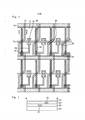
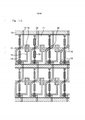
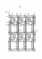
[0024] O primeiro substrato de matriz ativa da presente invenção inclui: os eletrodos de pixel dispostos em um padrão de matriz; uma linha de fonte estendendo-se em uma direção da coluna e coincidindo com qualquer um dos dois adjacentes eletrodos de pixel em uma dire- ção da fileira; e uma linha de capacitor de armazenamento estenden- do-se na direção da fileira e intersectando com a linha de fonte. O pri- meiro substrato de matriz ativa da presente invenção é provido com uma variedade de eletrodos e linhas para acionamento de LC tais co- mo eletrodos de pixel, linhas de fonte, linhas de porta e linhas de ca- pacitor de armazenamento. No substrato incluindo estes eletrodos e linhas, as linhas de porta são dispostas em uma direção da fileira, isto é, em uma direção do comprimento da linha de capacitor de armaze- namento para intersectar com as linhas de fonte e em cada interseção das duas linhas, um TFT ( transistor de filme fino), que é um elemento de comutação e similar é provido. Os eletrodos de pixel, cada qual, constituem uma unidade de pixel para aplicação de uma voltagem à camada de LC e funciona como um pixel para acionamento de LCs. As linhas de fonte, cada qual, fornecem um sinal de fonte ao eletrodo de pixel ou TFT. As linhas de capacitor de armazenamento, cada qual, formam uma capacitância juntamente com um outro eletrodo ou linha disposta com o filme isolante entre os mesmos para armazenar um potencial elétrico do eletrodo de pixel quando o TFT é desativado. As linhas de porta, cada qual, controlam uma regulação de tempo de apli- cação de dado de sinal ao eletrodo de pixel e ao TFT. Os TFTs são elementos comutadores de semicondutor de três terminais e cada qual pode controlar um sinal de porta alimentado da linha de porta e um sinal de fonte alimentado da linha de fonte. Os locais das linhas de porta, das linhas de fonte e dos TFTs permitem o acionamento se- quencial da linha em que a voltagem de sinal é aplicada em sequência aos eletrodos de pixel ao longo da linha de porta.[0024] The first active matrix substrate of the present invention includes: pixel electrodes arranged in a matrix pattern; a source line extending in one direction of the column and coinciding with any of the two adjacent pixel electrodes in one direction of the row; and a line of storage capacitor extending in the direction of the row and intersecting with the source line. The first active matrix substrate of the present invention is provided with a variety of electrodes and lines for driving LC such as pixel electrodes, source lines, port lines and storage capacitor lines. On the substrate including these electrodes and lines, the port lines are arranged in a direction of the row, that is, in a direction of the length of the storage capacitor line to intersect with the source lines and at each intersection of the two lines , a TFT (thin film transistor), which is a switching element and the like is provided. The pixel electrodes each constitute a pixel unit for applying a voltage to the LC layer and functions as a pixel for driving LCs. The source lines each provide a source signal to the pixel or TFT electrode. The storage capacitor lines each form a capacitance along with another electrode or line arranged with the insulating film between them to store an electrical potential of the pixel electrode when the TFT is deactivated. The door lines each control the timing of the application of signal data to the pixel electrode and the TFT. TFTs are three-terminal semiconductor switching elements and each can control a port signal powered from the port line and a source signal fed from the source line. The locations of the door lines, the source lines and the TFTs allow the sequential activation of the line where the signal voltage is applied in sequence to the pixel electrodes along the door line.
[0025] Os eletrodos de pixel, a linha de fonte e a linha de capacitor de armazenamento são dispostos em diferentes camadas empilhadas com um filme isolante entre os mesmos e a linha de fonte possui pon- tos curvos abaixo de ambos os adjacentes dois eletrodos de pixel em fileira e possui uma porção de cruzamento que passa através de um espaço entre os adjacentes dois eletrodos de pixel em fileira. De acor- do com a presente invenção, a linha de fonte é disposta em uma ca- mada diferente do eletrodo de pixel com um filme isolante entre os mesmos e uma certa capacitância é formada entre a linha de fonte e o eletrodo de pixel, como as linhas de capacitor de armazenamento fa- zem. A linha de fonte é disposta na direção da fileira no todo como acima mencionado, porém encurva-se pelo menos duas vezes nos respectivos pontos de curva e a porção de cruzamento, que é uma porção entre os pontos de curva, passa através de um espaço entre os dois eletrodos de pixel adjacentes. No ponto de curva, a linha de fonte encurva-se em um ângulo reto ou obliquamente à direção longitudinal da linha de fonte. Como um resultado, a linha de fonte pode coincidir com cada um dos dois eletrodos de pixel em fileira adjacentes.[0025] The pixel electrodes, the source line and the storage capacitor line are arranged in different layers stacked with an insulating film between them and the source line has curved points below both adjacent two electrodes. pixel in a row and has a crossing portion that passes through a space between adjacent two pixel electrodes in a row. According to the present invention, the source line is arranged in a different layer than the pixel electrode with an insulating film between them and a certain capacitance is formed between the source line and the pixel electrode, as the storage capacitor lines do. The source line is arranged in the direction of the whole row as mentioned above, however it curves at least twice at the respective curve points and the crossing portion, which is a portion between the curve points, passes through a space between the two adjacent pixel electrodes. At the curve point, the source line curves at a right angle or obliquely to the longitudinal direction of the source line. As a result, the source line can match each of the two adjacent row pixel electrodes.
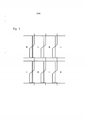
[0026] O significado da provisão da linha de fonte com os pontos curvos para coincidir com ambos os adjacentes dois eletrodos de pixel em fileira é abaixo mencionado. As figuras 15 e 16 são vistas em plan- ta, cada qual esquematicamente mostrando uma relação entre os lo- cais dos eletrodos de pixel e linhas de fonte e uma capacitância for- mada entre os mesmos. A figura 16 mostra uma concretização con- vencional em que as linhas de fonte não têm pontos curvos. A figura 15 mostra uma concretização da presente invenção em que as linhas de fonte, cada qual, têm pontos curvos. As figuras 15(a) e 16(a) mos- tram uma relação sem o desalinhamento. As figuras 15(b) e 16(b) mostram uma relação com o desalinhamento. As porções de sombra nas figuras 15 e 16, cada qual, mostram uma região de sobreposição da linha de fonte e do eletrodo de pixel. Como mostrado na figura 16, quando os eletrodos de pixel ( pix1 a pix3 ) são dispostos em um pa- drão de matriz, as linhas de fonte (S1 a S3) são usualmente dispostas para coincidirem com respectivos espaços entre os eletrodos de pixel. A camada incluindo os eletrodos de pixel e a camada incluindo as li- nhas de fonte são separadas, e um filme isolante é formado entre os mesmos. Assim, uma certa capacitância é formada entre um eletrodo de pixel e a linha de fonte. Todavia, a linha de fonte nem sempre está disposta para passar no centro do espaço entre os eletrodos de pixel como mostrado na figura 16(b), por exemplo, uma vez que os eletro- dos de pixel e as linhas de fonte são dispostos nas diferentes camadas. A quantidade da capacitância é proporcional a uma área de sobreposi- ção entre a linha de fonte e o eletrodo de pixel. Assim, uma grande variação na área causa os seguintes problemas, por exemplo, quando uma polaridade é invertida entre os eletrodos de pixel adjacentes.[0026] The significance of the provision of the source line with the curved points to coincide with both adjacent two pixel electrodes in a row is mentioned below. Figures 15 and 16 are seen in plan, each schematically showing a relationship between the locations of the pixel electrodes and source lines and a capacitance formed between them. Figure 16 shows a conventional embodiment in which the source lines have no curved points. Figure 15 shows an embodiment of the present invention in which the source lines each have curved points. Figures 15 (a) and 16 (a) show a relationship without misalignment. Figures 15 (b) and 16 (b) show a relationship with misalignment. The shadow portions in figures 15 and 16 each show a region of overlap between the source line and the pixel electrode. As shown in figure 16, when the pixel electrodes (pix1 to pix3) are arranged in a matrix pattern, the source lines (S1 to S3) are usually arranged to match the respective spaces between the pixel electrodes. The layer including the pixel electrodes and the layer including the source lines are separated, and an insulating film is formed between them. Thus, a certain capacitance is formed between a pixel electrode and the source line. However, the source line is not always willing to pass in the center of the space between the pixel electrodes as shown in figure 16 (b), for example, since the pixel electrodes and the source lines are arranged in the different layers. The amount of capacitance is proportional to an area of overlap between the source line and the pixel electrode. Thus, a large variation in the area causes the following problems, for example, when a polarity is reversed between the adjacent pixel electrodes.
[0027] Nos dispositivos de LCD, uma capacitância Cpix, que um eletrodo de pixel forma, é uma soma de Ccs formada com uma linha de capacitor de armazenamento, c1c formado em uma camada de LC, Csd formada com uma linha de fonte, Cgd formada entre as linhas de porta e dreno e similar, como mostrado na seguinte fórmula (1). Cpix= Ccs + Ccl + Csd + Cgd (1)[0027] In LCD devices, a Cpix capacitance, which a pixel electrode forms, is a sum of Ccs formed with a storage capacitor line, c1c formed in an LC layer, Csd formed with a source line, Cgd formed between the door and drain lines and similar, as shown in the following formula (1). Cpix = Ccs + Ccl + Csd + Cgd (1)
[0028] O potencial elétrico de pixel Vpixl pode ser representado pe- la seguinte fórmula (2): Vpixl = Vs1 — (( Csdl/ Cpixl x Vsipp) + (Csd2/ Cpixl x Vs2pp )) (2)[0028] The electrical potential of pixel Vpixl can be represented by the following formula (2): Vpixl = Vs1 - ((Csdl / Cpixl x Vsipp) + (Csd2 / Cpixl x Vs2pp)) (2)
[0029] em que Sl representa uma linha de fonte coincidindo com um lado do pix1 de eletrodo de pixel;[0029] where Sl represents a source line coinciding with a side of the pixel electrode pix1;
[0030] S2 representa linha de fonte coincidindo com um lado de pix1 de eletrodo de pixel;[0030] S2 represents source line coinciding with a pixel electrode pix1 side;
[0031] Vs1 e Vs2 representam potenciais elétricos de fonte aplica- dos por S1 e S2, respectivamente;[0031] Vs1 and Vs2 represent electrical potentials of sources applied by S1 and S2, respectively;
[0032] Cpixl representa capacitância, que pix1 forma;[0032] Cpixl represents capacitance, which forms pix1;
[0033] Csd1 e Csd2 representam capacitâncias formadas entre pix1 e Sl e entre pix1 e S2, respectivamente;[0033] Csd1 and Csd2 represent capacitances formed between pix1 and Sl and between pix1 and S2, respectively;
[0034] Pix1 recebe potencial elétrico de sinal de S1;[0034] Pix1 receives electrical potential from S1 signal;
[0035] Pix1 tem uma polaridade de "mais";[0035] Pix1 has a "more" polarity;
[0036] Pix2 tem uma polaridade de "menos".[0036] Pix2 has a "minus" polarity.
[0037] Vs2 = -Vs1 é satisfeita porque os pixels adjacentes são dife- rentes em polaridade. "(Csd1/Cpix1 x Vs1pp) + (Csd2/Cpix1 x Vs2pp)" mostra uma voltagem traçada por S1 e S2.[0037] Vs2 = -Vs1 is satisfied because the adjacent pixels are different in polarity. "(Csd1 / Cpix1 x Vs1pp) + (Csd2 / Cpix1 x Vs2pp)" shows a voltage drawn by S1 and S2.
[0038] Neste caso, a polaridade de um potencial elétrico de fonte aplicado ao eletrodo de pixel é invertida a cada período de 1H e então, as influências equivalentes a duas vezes o potencial elétrico de fonte atuam no eletrodo de pixel. Assim, os potenciais elétricos de fonte Vs1pp e Vs2pp equivalentes às voltagens do desenho satisfazem Vs1pp = 2 x Vs1 e Vs2pp = 2 x Vs2.[0038] In this case, the polarity of an electrical source potential applied to the pixel electrode is inverted every 1H period and then, the influences equivalent to twice the electrical source potential act on the pixel electrode. Thus, the electrical potentials of the Vs1pp and Vs2pp source equivalent to the drawing voltages satisfy Vs1pp = 2 x Vs1 and Vs2pp = 2 x Vs2.
[0039] Similarmente, o potencial elétrico Vpix2 pode ser representa- do pela seguinte fórmula (3). Vpix2 = Vs2 — ((Csd2/Cpix2 x Vs2pp) + (Csd3/Cpix2 X Vs3pp) (3)[0039] Similarly, the electric potential Vpix2 can be represented by the following formula (3). Vpix2 = Vs2 - ((Csd2 / Cpix2 x Vs2pp) + (Csd3 / Cpix2 X Vs3pp) (3)
[0040] em que S2 representa a linha de fonte que coincide com um lado do eletrodo de pixel pix2;[0040] where S2 represents the source line that coincides with one side of the pix2 pixel electrode;
[0041] S3 representa linha de fonte que coincide com um outro lado do eletrodo de pixel pix2;[0041] S3 represents source line that coincides with another side of the pix2 pixel electrode;
[0042] Vs2 e Vs3 representam potenciais elétricos de fonte aplica- dos por S2 e S3, respectivamente;[0042] Vs2 and Vs3 represent electrical potentials of sources applied by S2 and S3, respectively;
[0043] Cpix2 representa capacitância, que pix2 forma; formada em pix2;[0043] Cpix2 represents capacitance, which pix2 forms; formed in pix2;
[0044] Csd2 e Csd3 representam capacitâncias formadas entre pix2 e S2 e entre pix3 e S3, respectivamente;[0044] Csd2 and Csd3 represent capacitances formed between pix2 and S2 and between pix3 and S3, respectively;
[0045] Pix2 recebe potencial de sinal do S2; e[0045] Pix2 receives signal potential from S2; and
[0046] Pix3 adjacente a pix2 possui polaridade de mais.[0046] Pix3 adjacent to pix2 has more polarity.
[0047] Vs3=-Vs2 é satisfeita porque os pixels adjacentes são dife- rentes em polaridade. "(Csd2/Cpix2 x Vs2pp)+ (Csd3/Cpix2 x Vs3pp)" repre- senta uma voltagem estirada por S2 e S3.[0047] Vs3 = -Vs2 is satisfied because the adjacent pixels are different in polarity. "(Csd2 / Cpix2 x Vs2pp) + (Csd3 / Cpix2 x Vs3pp)" represents a voltage drawn by S2 and S3.
[0048] Em vista do acima, quando a polaridade é diferente entre os dois pixels adjacentes e quando uma área em que a linha de fonte coincide com o eletrodo de pixel é a mesma entre os dois pixels adja- centes, como mostrado na figura 16(a), Csd1 = Csd2 = Csd3 é satisfeita e as voltagens estiradas pelas linhas de fonte podem ser mutuamente canceladas entre os pixels e os adjacentes dois pixels são os mesmos em potencial elétrico (cujas polaridades podem ser diferentes). Toda- via, como mostrado na figura 16(b),quando a área de sobreposição é variada entre os pixels Csd1> Csd2 ou Csd1 < Csd2 é satisfeita ou Csd2 > Csd3 ou Csd2 < Csd3 é satisfeita e a voltagem estirada pela linha de fonte muda é também variada e os dois pixels adjacentes têm diferentes po- tenciais, resultando em display sem uniformidade.[0048] In view of the above, when the polarity is different between the two adjacent pixels and when an area where the source line coincides with the pixel electrode is the same between the two adjacent pixels, as shown in figure 16 (a), Csd1 = Csd2 = Csd3 is satisfied and the voltages drawn by the source lines can be mutually canceled between the pixels and the adjacent two pixels are the same in electrical potential (whose polarities can be different). However, as shown in figure 16 (b), when the overlap area is varied between pixels Csd1> Csd2 or Csd1 <Csd2 is satisfied or Csd2> Csd3 or Csd2 <Csd3 is satisfied and the voltage drawn by the source line changes are also varied and the two adjacent pixels have different potentials, resulting in a non-uniform display.
[0049] Na presente invenção, como mostrado nas figuras 15(a) e 15(b), a linha de fonte é provida com os pontos curvos para coincidir com cada um dos dois eletrodos de pixel adjacentes, o que facilmente possibilita que quase a linha de fonte toda coincida com os eletrodos de pixel. De acordo com isto, os dois pixels adjacentes têm o mesmo potencial, mesmo que um ligeiro desalinhamento ocorra como mostra- do na figura 15(b). Especificamente, valores quase equivalentes são facilmente dados a Csd1, Csd2, e Csd3 na concretização da presente in- venção.[0049] In the present invention, as shown in figures 15 (a) and 15 (b), the source line is provided with curved points to match each of the two adjacent pixel electrodes, which easily enables almost the entire source line coincides with the pixel electrodes. Accordingly, the two adjacent pixels have the same potential, even if a slight misalignment occurs as shown in figure 15 (b). Specifically, nearly equivalent values are easily given to Csd1, Csd2, and Csd3 in carrying out the present invention.
[0050] A linha de capacitor de armazenamento possui uma porção que se estende na direção da coluna e que coincide com o espaço en- tre os adjacentes dois eletrodos de pixel em fileira. Quando é projetado de modo que a linha de fonte seja curva e deste modo a linha de fonte toda coincida com os eletrodos de pixel, um espaço entre os eletrodos de pixel possui uma região livre do membro de proteção contra luz. Através desta região, a luz é vazada no estado de display preto e uma razão de contraste calculada por "luminância no estado de display branco/luminância no display preto" é reduzida. Na presente invenção, é projetado que a parte da linha de capacitor de armazenamento seja ramificada e então estendida para coincidir com um espaço entre os eletrodos de pixel e deste modo a luz através do espaço é bloqueada para reduzir o vazamento da luz no estado de display preto e a razão de contraste pode ser melhorada. A matriz de preto feita de resinas orgânicas e similares pode ser comumente usada como o membro de proteção contra a luz, porém a matriz de preto e a linha de fonte são tipicamente dispostas em diferentes substratos e suficientes efeitos de proteção contra a luz não devem ser obtidos se desalinhamento entre os dois substratos ocorrer. Em adição, a luz deve ser vazada através de um furo de pino possivelmente formado na matriz de preto. Em con- traste à matriz de preto, a linha de capacitor de armazenamento pode ser facilmente disposta no substrato incluindo a linha de fonte. Então, o uso da linha de capacitor de armazenamento como membro de pro- teção contra a luz pode minimizar as influências pelo desalinhamento. Ainda, os filmes de metal mostram muito maior propriedade de prote- ção contra a luz do que as resinas orgânicas. Consequentemente, es- tas linhas são mais apropriadas como membro de proteção contra a luz da presente invenção.[0050] The storage capacitor line has a portion that extends towards the column and that coincides with the space between the adjacent two pixel electrodes in a row. When it is designed so that the source line is curved and thus the entire source line coincides with the pixel electrodes, a space between the pixel electrodes has a free region of the light protection member. Through this region, the light is emitted in the black display state and a contrast ratio calculated by "luminance in the white display state / luminance in the black display" is reduced. In the present invention, the part of the storage capacitor line is designed to be branched and then extended to match a space between the pixel electrodes and thus the light through the space is blocked to reduce light leakage in the display state. black and the contrast ratio can be improved. The black matrix made of organic resins and the like can be commonly used as the light protection member, however the black matrix and the source line are typically arranged on different substrates and sufficient light protection effects should not be used. obtained if misalignment between the two substrates occurs. In addition, the light must be poured through a pin hole possibly formed in the black matrix. In contrast to the black matrix, the storage capacitor line can be easily arranged on the substrate including the source line. So, the use of the storage capacitor line as a light protection member can minimize the influences due to misalignment. In addition, metal films show much greater protection properties against light than organic resins. Consequently, these lines are more suitable as a light protection member of the present invention.
[0051] A linha de fonte coincide com a linha de capacitor de arma- zenamento substancialmente apenas em uma sua interseção. Na pre- sente invenção, a porção maior da linha de fonte fica distante da linha de capacitor de armazenamento, de modo a não coincidir com a mes- ma, a fim de evitar o retardo do sinal e similar possivelmente causado devido à capacitância parasítica formada com a mesma. Na presente invenção, a linha de capacitor de armazenamento e a linha de fonte são projetadas para serem intersectadas uma com a outra e, assim, as duas linhas são coincididas uma com a outra pelo menos em um ponto. De acordo com a concretização em que a linha de fonte coincide com a linha de capacitor de armazenamento substancialmente apenas na intersecção da mesma, como na presente invenção, a formação de capacitância parasítica pode ser suficientemente reduzida, conduzindo à supressão do retardo de sinal.[0051] The source line coincides with the storage capacitor line substantially only at its intersection. In the present invention, the largest portion of the source line is far from the storage capacitor line, so as not to coincide with the same, in order to avoid signal delay and similar possibly caused due to the parasitic capacitance formed with it. In the present invention, the storage capacitor line and the source line are designed to be intersected with each other and, thus, the two lines are coincided with each other at least at one point. According to the embodiment in which the source line coincides with the storage capacitor line substantially only at the intersection thereof, as in the present invention, the formation of parasitic capacitance can be sufficiently reduced, leading to the suppression of the signal delay.
[0052] A configuração do substrato de matriz ativa da presente invenção não está especialmente limitada. O substrato de matriz ativa pode ou não incluir outros componentes desde que essencialmente inclua os componentes acima mencionados.[0052] The configuration of the active matrix substrate of the present invention is not particularly limited. The active matrix substrate may or may not include other components as long as it essentially includes the above mentioned components.
[0053] O substrato de matriz ativa da presente invenção pode ser montado em uma variedade de dispositivos de display e sensores, por exemplo. Os exemplos dos dispositivos de display incluem dispositivos de LCD e displays de EL orgânicos. Exemplos dos sensores incluem sensores de foto, sensores magnéticos, sensores de temperatura e sensores químicos.[0053] The active matrix substrate of the present invention can be mounted on a variety of display devices and sensors, for example. Examples of display devices include LCD devices and organic EL displays. Examples of the sensors include photo sensors, magnetic sensors, temperature sensors and chemical sensors.
[0054] No primeiro substrato de matriz ativa da presente invenção, uma linha de porta pode ser usada como porção que se estende em vez da linha de capacitor de armazenamento. A presente invenção é um substrato de matriz ativa, incluindo:[0054] In the first active matrix substrate of the present invention, a port line can be used as an extending portion instead of the storage capacitor line. The present invention is an active matrix substrate, including:
[0055] eletrodos de pixel dispostos em um padrão de matriz;[0055] pixel electrodes arranged in a matrix pattern;
[0056] uma linha de fonte que se estende em uma direção de co- luna e coincidente com qualquer um dos adjacentes dois dos eletrodos de pixel em uma direção da fileira; e[0056] a source line that extends in a column direction and coincides with any of the adjacent two of the pixel electrodes in a direction of the row; and
[0057] uma linha de porta estendendo-se na direção da fileira e intersectando com a linha da fonte,[0057] a door line extending towards the row and intersecting with the source line,
[0058] em que os eletrodos de pixel, a linha de fonte e a linha de porta são dispostos em diferentes camadas empilhadas com um filme isolante entre os mesmos,[0058] in which the pixel electrodes, the source line and the door line are arranged in different layers stacked with an insulating film between them,
[0059] a linha de fonte possui pontos curvos abaixo de ambos os adjacentes dois eletrodos de pixel da fileira e possui uma porção de cruzamento que passa através de um espaço entre os adjacentes dois eletrodos de pixel da fileira,[0059] the source line has curved points below both adjacent two pixel electrodes in the row and has a crossing portion that passes through a space between the adjacent two pixel electrodes in the row,
[0060] a linha de porta possui uma porção que se estende na dire- ção da coluna e coincidindo com o espaço entre os dois eletrodos de pixel adjacentes da fileira, e[0060] the gate line has a portion that extends towards the column and coincides with the space between the two adjacent pixel electrodes in the row, and
[0061] a linha de fonte coincide com a linha de porta substancial- mente apenas em uma sua interseção ( a seguir, também referida co- mo um segundo substrato de matriz ativa da presente invenção).[0061] the source line coincides with the door line substantially only at its intersection (hereinafter also referred to as a second active matrix substrate of the present invention).
[0062] De acordo com esta concretização, em que a linha de porta é estendida, diferente da concretização em que a linha de capacitor de armazenamento é estendida, uma mudança de voltagem de um sinal de porta anterior momentaneamente proporciona uma influencia sobre a capacitância formada entre a linha de porta e o eletrodo de pixel, po- rém em vista da proteção contra a luz e do retardo de sinal, as mes- mas vantagens como no uso da linha de capacitor de armazenamento podem ser obtidas.[0062] According to this embodiment, in which the door line is extended, different from the embodiment in which the storage capacitor line is extended, a voltage change of a previous door signal momentarily provides an influence on the capacitance formed between the gate line and the pixel electrode, however, in view of the protection against light and signal delay, the same advantages as in the use of the storage capacitor line can be obtained.
[0063] No primeiro substrato de matriz ativa da presente invenção, um eletrodo flutuante pode ser usado em vez da linha de capacitor de armazenamento. A presente invenção é também um substrato de ma- triz ativa, incluindo:[0063] In the first active matrix substrate of the present invention, a floating electrode can be used instead of the storage capacitor line. The present invention is also an active matrix substrate, including:
[0064] eletrodos de pixel dispostos em um padrão de matriz; e[0064] pixel electrodes arranged in a matrix pattern; and
[0065] uma linha de fonte que se estende em uma direção da co- luna e coincidente com qualquer um dos adjacentes dois eletrodos de pixel em uma direção da fileira,[0065] a source line extending in a direction of the column and coinciding with any of the adjacent two pixel electrodes in a direction of the row,
[0066] em que os eletrodos de pixel e a linha de fonte são dispos- tos em diferentes camadas com um filme isolante entre os mesmos,[0066] in which the pixel electrodes and the source line are arranged in different layers with an insulating film between them,
[0067] a linha de fonte possui pontos curvos abaixo de ambos dos dois eletrodos de pixel adjacentes da fileira e possui uma porção transversal que passa através de um espaço entre os dois eletrodos de pixel adjacentes da fileira,e[0067] the source line has curved points below both of the two adjacent pixel electrodes in the row and has a transverse portion that passes through a space between the two adjacent pixel electrodes in the row, and
[0068] o substrato de matriz ativa inclui um eletrodo flutuante que se estende na direção da coluna e coincidente com o espaço entre os dois eletrodos de pixel adjacentes da fileira ( a seguir, também referido com terceiro substrato de matriz ativa da presente invenção). De acor- do com isto, as mesmas vantagens que no uso da linha de capacitor de armazenamento ou da linha de porta podem ser obtidas em vista da proteção contra a luz e retardo de sinal.[0068] the active matrix substrate includes a floating electrode that extends towards the column and coincides with the space between the two adjacent pixel electrodes in the row (hereinafter also referred to as the third active matrix substrate of the present invention). Accordingly, the same advantages as using the storage capacitor line or the door line can be obtained in view of the protection against light and signal delay.
[0069] O eletrodo flutuante é um eletrodo independente e não co- nectado a outras linhas tais como linha de capacitor de armazenamen- to e linha de porta. Os materiais para as linhas de capacitor de arma- zenamento ou linhas de porta podem ser usados para o eletrodo flutu- ante. Isto permite a simplificação das etapas de produção. Uma capa- citância parasítica formada entre a linha de fonte e o eletrodo flutuante possivelmente causa retardo de sinal, como ocorre com a capacitância formada entre a linha de fonte e a linha de capacitor ou linha de porta. Assim, é preferível que a linha de fonte coincida com o eletrodo flutu- ante substancialmente apenas em uma sua intersecção e é mais pre- ferível que a linha de fonte não coincida substancialmente com o ele- trodo flutuante.[0069] The floating electrode is an independent electrode and is not connected to other lines such as storage capacitor line and gate line. The materials for the storage capacitor lines or port lines can be used for the floating electrode. This allows for simplification of the production steps. A parasitic capacitance formed between the source line and the floating electrode possibly causes signal delay, as occurs with the capacitance formed between the source line and the capacitor line or gate line. Thus, it is preferable that the source line coincides with the floating electrode substantially only at its intersection and it is more preferable that the source line does not substantially coincide with the floating electrode.
[0070] As concretizações preferíveis do primeiro a terceiro substra- tos de matriz ativa da presente invenção são mencionadas em maiores detalhes abaixo.[0070] Preferred embodiments of the first to third active matrix substrates of the present invention are mentioned in more detail below.
[0071] É preferível que os adjacentes dois eletrodos de pixel da fileira sejam diferentes em polaridade. Especificamente, de acordo com a presente concretização, um dos dois eletrodos de pixel adjacen- tes possui uma polaridade de mais e o outro possui uma polaridade de menos e a linha de fonte coincide com cada um dos dois eletrodos de pixel com as diferentes polaridades através dos pontos de curva. O acionamento inverso de ponto pode ser empregado, por exemplo, co- mo este sistema de acionamento a fim de aplicar voltagens com dife- rentes polaridades aos respectivos dois eletrodos de pixel adjacentes. No acionamento inverso de ponto, os eletrodos de pixel são dispostos de modo que uma polaridade de mais e uma polaridade de menos se- jam alternadas em ambas as direções vertical e transversal na ordem de mais, menos, mais, menos. De acordo com a presente invenção, a polaridade é invertida entre os adjacentes dois eletrodos de pixel, e assim, por exemplo, pelo menos qualquer um dos dois eletrodos de pixel na direção da fileira e na direção da coluna é disposto, de modo que suas polaridades fiquem na ordem de mais, menos, menos, mais ou na ordem de menos, mais, mais, menos. Assim, quando os dois eletrodos de pixel adjacentes são diferentes em polaridade, a geração de tremulação pode ser efetivamente suprimida. As vantagens da pre- sente invenção são particularmente exibidas neste sistema de acio- namento em que as voltagens com diferentes polaridades são aplica- das aos respectivos dois eletrodos de pixel adjacentes. Mesmo quan- do ligeiro mau alinhamento ocorrer, os eletrodos de pixel podem mos- trar quase o mesmo potencial elétrico e deste modo a deterioração nas qualidades de display pode ser prevenida.[0071] It is preferable that the adjacent two pixel electrodes of the row are different in polarity. Specifically, according to the present embodiment, one of the two adjacent pixel electrodes has a polarity of more and the other has a polarity of less and the source line coincides with each of the two pixel electrodes with the different polarities across curve points. The reverse point activation can be used, for example, with this drive system in order to apply voltages with different polarities to the respective two adjacent pixel electrodes. In reverse point activation, the pixel electrodes are arranged so that a polarity of more and a polarity of less are alternated in both the vertical and transverse directions in the order of plus, minus, plus, minus. According to the present invention, the polarity is reversed between the adjacent two pixel electrodes, and so, for example, at least any one of the two pixel electrodes in the direction of the row and in the direction of the column is arranged, so that their polarities are in the order of more, less, less, more or in the order of less, more, more, less. Thus, when the two adjacent pixel electrodes are different in polarity, the jitter generation can be effectively suppressed. The advantages of the present invention are particularly shown in this drive system in which voltages with different polarities are applied to the respective two adjacent pixel electrodes. Even when slight misalignment occurs, the pixel electrodes can show almost the same electrical potential and in this way deterioration in the display qualities can be prevented.
[0072] Concretizações preferíveis do primeiro substrato de matriz ativa da presente invenção em que a linha de capacitor de armazena- mento é estendida são mencionadas abaixo. A seguir, são dadas as concretizações preferíveis do primeiro substrato de matriz ativa inclu- indo uma linha de porta que se estende na direção da fileira e intersec- tando com a linha de fonte.[0072] Preferred embodiments of the first active matrix substrate of the present invention in which the storage capacitor line is extended are mentioned below. In the following, the preferred embodiments of the first active matrix substrate are given, including a port line extending in the direction of the row and intersecting with the source line.
[0073] É preferível que a linha da porta tenha uma porção que se estende na direção da coluna e coincida com o espaço entre os adja- centes dois eletrodos de pixel da fileira. Especificamente, de acordo com a presente concretização, o espaço na direção da coluna entre os adjacentes dois eletrodos de pixel é sobreposto pelas respectivas por- ções de extensão da linha de capacitor de armazenamento e a linha de porta. Pelo uso de ambas, a linha de capacitor de armazenamento e a linha de porta, como membro de proteção contra luz, a região pro- tegida da luz pode ser suficientemente assegurada e uma capacitância de armazenamento em uma quantidade apropriada pode ser formada.[0073] It is preferable that the door line has a portion that extends towards the column and coincides with the space between the adjacent two pixel electrodes in the row. Specifically, according to the present embodiment, the space in the direction of the column between the adjacent two pixel electrodes is overlaid by the respective extension portions of the storage capacitor line and the door line. By using both the storage capacitor line and the door line, as a light protection member, the light-protected region can be sufficiently secured and a storage capacitance in an appropriate amount can be formed.
[0074] É preferível que a linha de porta e a linha de capacitor de armazenamento sejam dispostas na mesma camada. Como mencio- nado acima, a linha de capacitor de armazenamento e a linha de porta são providas com uma função como de um membro de proteção con- tra luz, em adição a seus papéis originais e os mesmos materiais po- dem ser usados para a linha de porta e a linha de capacitor de arma- zenamento. Assim, nesta concretização, a linha de capacitor de arma- zenamento e a linha de porta podem ser formadas a um tempo, o que simplifica as etapas de produção.[0074] It is preferable that the port line and the storage capacitor line are arranged on the same layer. As mentioned above, the storage capacitor line and the door line are provided with a function as a light protection member, in addition to their original papers and the same materials can be used for port line and storage capacitor line. Thus, in this embodiment, the storage capacitor line and the door line can be formed at the same time, which simplifies the production steps.
[0075] É preferível que a linha de porta e a linha de capacitor de armazenamento sejam dispostas em diferentes camadas com um filme isolante entre as mesmas. Geralmente, os defeitos de vazamento en- tre as linhas dispostas na mesma camada podem ocorrer. Esta con- cretização reduz a possibilidade da geração de tais defeitos de vaza- mento. De acordo com a concretização acima mencionada, é preferí- vel que o espaço entre os dois eletrodos de pixel adjacentes da fileira coincida com pelo menos uma linha de porta e linha de capacitor de armazenamento. De acordo com esta concretização, a linha de porta e a linha de capacitor de armazenamento podem ser dispostas de modo a coincidirem parcialmente entre si e cada espaço na direção da fileira entre aqueles adjacentes dos eletrodos de pixel pode ser protegido da luz ou pela linha de porta ou pelo capacitor de armazenamento. Assim, o vazamento da luz entre os eletrodos de pixel pode ser mais segura- mente prevenido. Por exemplo, os dispositivos de display incluindo o substrato de matriz ativa da presente concretização podem prover dis- play de contraste maior.[0075] It is preferable that the port line and the storage capacitor line are arranged in different layers with an insulating film between them. Generally, leakage defects between lines arranged on the same layer can occur. This materialization reduces the possibility of the generation of such leakage defects. According to the aforementioned embodiment, it is preferable that the space between the two adjacent pixel electrodes in the row coincides with at least one port line and storage capacitor line. According to this embodiment, the port line and the storage capacitor line can be arranged to partially coincide with each other and each space in the direction of the row between those adjacent to the pixel electrodes can be protected from light or by the line of port or storage capacitor. Thus, the leakage of light between the pixel electrodes can be more safely prevented. For example, display devices including the active matrix substrate of the present embodiment can provide greater contrast display.
[0076] É preferível que a linha de porta seja disposta para coincidir com um espaço entre aquele adjacente dos dois eletrodos de pixel na direção da coluna. De acordo com a presente concretização, não ape- nas os espaços na direção da fileira, mas também os espaços na dire- ção da coluna entre os adjacentes eletrodos de pixel podem ser prote- gidos da luz. Assim, o vazamento da luz entre os eletrodos de pixel pode ser mais seguramente prevenido. Por exemplo, dispositivos de display incluindo o substrato de matriz ativa da presente concretização podem prover display de contraste maior.[0076] It is preferable that the port line is arranged to coincide with a space between that adjacent to the two pixel electrodes in the direction of the column. According to the present embodiment, not only the spaces in the direction of the row, but also the spaces in the direction of the column between the adjacent pixel electrodes can be protected from light. Thus, the leakage of light between the pixel electrodes can be more safely prevented. For example, display devices including the active matrix substrate of the present embodiment can provide a higher contrast display.
[0077] É preferível que a linha de capacitor de armazenamento seja disposta para coincidir com um espaço entre quaisquer adjacen- tes dois dos eletrodos de pixel na direção da coluna. Por exemplo, quando a linha de porta é disposta para coincidir com os eletrodos de pixel, não no espaço entre os adjacentes dois eletrodos de pixel da coluna, esta concretização permite que o vazamento de luz entre os adjacentes dois eletrodos de pixel da coluna seja mais seguramente prevenido. Por exemplo, os dispositivos de display incluindo substrato de matriz ativa da presente concretização podem prover um display de contraste maior.[0077] It is preferable that the storage capacitor line is arranged to match a space between any adjacent two of the pixel electrodes in the column direction. For example, when the door line is arranged to match the pixel electrodes, not in the space between the adjacent two pixel electrodes of the column, this embodiment allows the light leakage between the adjacent two column electrodes to be more safely prevented. For example, display devices including active matrix substrate of the present embodiment can provide a higher contrast display.
[0078] Abaixo, são dadas as concretizações preferíveis do primei- ro substrato de matriz ativa da presente invenção ainda incluindo um eletrodo flutuante que coincide com o espaço entre os dois eletrodos de pixel adjacentes da fileira.[0078] Below, the preferred embodiments of the first active matrix substrate of the present invention are given, further including a floating electrode that matches the space between the two adjacent pixel electrodes of the row.
[0079] É preferível que o eletrodo flutuante e a linha de capacitor de armazenagem sejam dispostos na mesma camada. De acordo com esta concretização, a linha de capacitor de armazenamento e o eletro- do flutuante podem ser formados a um tempo, o que pode simplificar as etapas de produção.[0079] It is preferable that the floating electrode and the storage capacitor line are arranged in the same layer. According to this embodiment, the storage capacitor line and the floating electrode can be formed at the same time, which can simplify the production steps.
[0080] É preferível que o eletrodo flutuante e a linha de capacitor de armazenamento sejam dispostos em diferentes camadas com um filme isolante entre os mesmos e que o espaço entre os dois eletrodos de pixel adjacentes da fileira coincida com pelo menos um selecionado dentre eletrodo flutuante, linha de capacitor de armazenamento e linha de porta. De acordo com a presente concretização, cada espaço na direção da fileira entre os os eletrodos de pixel adjacentes pode ser protegido contra luz por qualquer eletrodo flutuante, pela linha de ca- pacitor de armazenamento e pela linha de porta. Como resultado, esta concretização permite que o vazamento de luz entre os dois eletrodos de pixel adjacentes da coluna seja mais seguramente prevenido. Por exemplo, os dispositivos de display incluindo o substrato de matriz ati- va da presente concretização podem prover display de contraste maior.[0080] It is preferable that the floating electrode and the storage capacitor line are arranged in different layers with an insulating film between them and that the space between the two adjacent pixel electrodes in the row coincides with at least one selected from the floating electrode. , storage capacitor line and port line. According to the present embodiment, each space in the direction of the row between the adjacent pixel electrodes can be protected against light by any floating electrode, the storage capacitor line and the door line. As a result, this embodiment allows the leakage of light between the two adjacent pixel electrodes of the column to be more safely prevented. For example, display devices including the active matrix substrate of the present embodiment can provide a higher contrast display.
[0081] Abaixo mencionadas são concretizações preferíveis do se- gundo substrato de matriz ativa em que a linha de porta é estendida. As concretizações preferíveis do segundo substrato de matriz ativa são as mesmas que no primeiro eletrodo de matriz ativa. A linha de capacitor de armazenamento do primeiro substrato de matriz ativa é substituída pela linha de porta. As concretizações em que o eletrodo flutuante é usado, mencionado no primeiro substrato de matriz ativa, podem ser também aplicadas ao segundo substrato da matriz ativa.[0081] Below mentioned are preferable embodiments of the second active matrix substrate in which the door line is extended. Preferable embodiments of the second active matrix substrate are the same as in the first active matrix electrode. The storage capacitor line of the first active matrix substrate is replaced by the port line. The embodiments in which the floating electrode is used, mentioned in the first active matrix substrate, can also be applied to the second active matrix substrate.
[0082] As seguintes concretizações são preferíveis quando o se- gundo substrato de matriz ativa ainda inclui uma linha de capacitor de armazenamento que se estende na direção da fileira e intersectando com a linha de fonte.[0082] The following embodiments are preferable when the second active matrix substrate still includes a line of storage capacitor that extends in the direction of the row and intersects with the source line.
[0083] É preferível que a linha de capacitor de armazenamento tenha uma porção que se estenda na direção da coluna coincidindo com o espaço entre os dois eletrodos de pixel adjacentes da fileira. De acordo com isto, ambas, a linha de porta e a linha de capacitor de ar- mazenamento podem ser usadas como membro de proteção contra a luz. A região protegida contra a luz pode ser suficientemente assegu- rada e uma capacitância de armazenamento em uma quantidade apropriada pode ser formada.[0083] It is preferable that the storage capacitor line has a portion that extends towards the column coinciding with the space between the two adjacent pixel electrodes in the row. Accordingly, both the port line and the storage capacitor line can be used as a light protection member. The light-protected region can be sufficiently secured and a storage capacitance in an appropriate amount can be formed.
[0084] É preferível que a linha de capacitor de armazenamento e a linha de porta sejam dispostas na mesma camada. De acordo com isto, a linha de porta e a linha de capacitor de armazenamento podem ser formadas a um tempo e assim as etapas de produção podem ser sim- plificadas.[0084] It is preferable that the storage capacitor line and the port line are arranged on the same layer. Accordingly, the port line and the storage capacitor line can be formed at the same time and thus the production steps can be simplified.
[0085] É preferível que a linha de capacitor de armazenamento e a linha de porta sejam dispostas nas diferentes camadas com um filme isolante entre as mesmas. Geralmente, os defeitos de vazamento en- tre as linhas dispostas na mesma camada podem ocorrer. Esta con- cretização reduz uma possibilidade de geração de tais defeitos de va- zamento. Na presente concretização, é preferível que o espaço entre os dois eletrodos de pixel adjacentes da fileira coincide com pelo me- nos uma da linha de capacitor de armazenamento e linha de porta. De acordo com isto, cada espaço nas direções da fileira e coluna entre dois eletrodos de pixel adjacentes pode ser protegido contra luz por linha de capacitor de armazenamento ou linha de porta. Assim, o va- zamento de luz entre os eletrodos de pixel pode ser mais seguramente prevenido. Por exemplo, os dispositivos de display incluindo o substra- to de matriz da presente concretização podem prover display de con- traste maior.[0085] It is preferable that the storage capacitor line and the door line are arranged on the different layers with an insulating film between them. Generally, leakage defects between lines arranged on the same layer can occur. This materialization reduces the possibility of generating such leakage defects. In the present embodiment, it is preferable that the space between the two adjacent pixel electrodes in the row coincides with at least one of the storage capacitor line and port line. Accordingly, each space in the row and column directions between two adjacent pixel electrodes can be protected from light by a storage capacitor line or door line. Thus, the leakage of light between the pixel electrodes can be more safely prevented. For example, display devices including the matrix substrate of the present embodiment can provide a larger contrast display.
[0086] É preferível que a linha de capacitor de armazenamento seja disposta para coincidir com um espaço entre quaisquer dois dos eletrodos de pixel adjacentes na direção da coluna. De acordo com isto, não apenas espaços na direção da fileira, mas também espaços na direção da coluna entre aqueles adjacentes dos eletrodos de pixel podem ser protegidos contra a luz. Assim, o vazamento da luz entre os eletrodos de pixel pode ser mais seguramente prevenido. Por exemplo, os dispositivos de display incluindo o substrato de matriz ativa da pre- sente concretização podem prover o display de contraste maior.[0086] It is preferable that the storage capacitor line is arranged to match a space between any two of the adjacent pixel electrodes in the column direction. Accordingly, not only spaces in the direction of the row, but also spaces in the direction of the column between those adjacent to the pixel electrodes can be protected from light. Thus, the leakage of light between the pixel electrodes can be more safely prevented. For example, display devices including the active matrix substrate of the present embodiment can provide the largest contrast display.
[0087] É preferível que a linha de porta seja disposta para coincidir com um espaço entre quaisquer dois dos eletrodos de pixel adjacentes na direção da coluna. Por exemplo, quando a linha de capacitor de armazenamento for disposta para coincidir com os eletrodos de pixel, não no espaço entre os adjacentes dois eletrodos de pixel da coluna, esta concretização permite que o vazamento de luz entre os dois ele- trodos de pixel adjacentes da coluna seja mais seguramente prevenido. Por exemplo, os dispositivos de display incluindo o substrato de matriz ativa da presente concretização podem prover um display de contraste maior.[0087] It is preferable that the port line is arranged to match a space between any two of the adjacent pixel electrodes in the direction of the column. For example, when the storage capacitor line is arranged to match the pixel electrodes, not in the space between adjacent two column pixel electrodes, this embodiment allows light leakage between the two adjacent pixel electrodes of the spine is more safely prevented. For example, display devices including the active matrix substrate of the present embodiment can provide a higher contrast display.
[0088] As seguintes concretizações são preferíveis quando o se- gundo substrato de matriz ativa ainda inclui um eletrodo flutuante coin- cidente com o espaço entre os adjacentes dois eletrodos de pixel da fileira.[0088] The following embodiments are preferable when the second active matrix substrate still includes a floating electrode matching the space between adjacent two pixel electrodes in the row.
[0089] É preferível que o eletrodo flutuante e a linha de porta se- jam dispostos na mesma camada. Como resultado, a linha da porta e o eletrodo flutuante podem ser formados a um tempo, o que pode sim- plificar as etapas de produção.[0089] It is preferable that the floating electrode and the port line are arranged in the same layer. As a result, the door line and the floating electrode can be formed at one time, which can simplify the production steps.
[0090] É preferível que o eletrodo flutuante e a linha de porta se- jam dispostos em diferentes camadas com um filme isolante entre os mesmos. Geralmente, os defeitos de vazamento entre linhas dispostas na mesma camada podem ocorrer. Esta concretização reduz uma possibilidade da geração de tais defeitos de vazamento. De acordo com a concretização acima mencionada, é preferível que o espaço en- tre os dois eletrodos de pixel adjacentes da fileira coincida com pelo menos um selecionado do eletrodo flutuante, linha de porta e linha de capacitor de armazenamento. De acordo com a presente concretiza- ção, cada espaço na direção da fileira entre aqueles dos eletrodos de pixel adjacentes pode ser protegido contra luz por qualquer um do ele- trodo flutuante, linha de porta e linha de capacitor de armazenamento. Como um resultado, esta concretização permite que o vazamento da luz entre os eletrodos de pixel seja mais seguramente prevenido. Por exemplo, os dispositivos de display incluindo o substrato de matriz ati- va da presente concretização podem prover display de contraste maior.[0090] It is preferable that the floating electrode and the port line are arranged in different layers with an insulating film between them. Generally, leakage defects between lines arranged on the same layer can occur. This embodiment reduces a possibility of the generation of such leakage defects. According to the aforementioned embodiment, it is preferable that the space between the two adjacent pixel electrodes in the row coincides with at least one selected from the floating electrode, port line and storage capacitor line. According to the present embodiment, each space in the direction of the row between those of the adjacent pixel electrodes can be protected from light by any of the floating electrode, port line and storage capacitor line. As a result, this embodiment allows the leakage of light between the pixel electrodes to be more safely prevented. For example, display devices including the active matrix substrate of the present embodiment can provide a higher contrast display.
[0091] Seguem abaixo as concretizações preferíveis do terceiro substrato de matriz ativa incluindo o eletrodo flutuante. As concretiza- ções preferíveis do terceiro substrato de matriz ativa são as mesmas que nos primeiro e segundo substratos de matriz ativa. A linha de ca- pacitor de armazenamento do primeiro substrato de matriz ativa e a linha de porta do segundo substrato de matriz ativa são substituídas com o eletrodo flutuante.[0091] Below are the preferred embodiments of the third active matrix substrate including the floating electrode. Preferred embodiments of the third active matrix substrate are the same as for the first and second active matrix substrates. The storage capacitor line of the first active matrix substrate and the port line of the second active matrix substrate are replaced with the floating electrode.
[0092] Preferíveis são as seguintes concretizações quando o ter- ceiro substrato de matriz ativa ainda inclui uma linha de capacitor de armazenamento que se estende na direção da coluna e que intersecta com a linha de fonte.[0092] Preferred are the following embodiments when the third active matrix substrate still includes a line of storage capacitor that extends towards the column and intersects with the source line.
[0093] É preferível que a linha de capacitor de armazenamento tenha uma porção que se estende na direção da coluna e que coincida com o espaço entre os dois eletrodos de pixel adjacentes da fileira. De acordo com isto, ambos o eletrodo flutuante e a linha de capacitor de armazenamento podem ser usados como membro de proteção contra a luz. Assim, a região protegida contra a luz pode ser suficientemente assegurada e uma capacitância de armazenamento em uma quantida- de apropriada pode ser formada.[0093] It is preferable that the storage capacitor line has a portion that extends towards the column and that matches the space between the two adjacent pixel electrodes in the row. Accordingly, both the floating electrode and the storage capacitor line can be used as a light protection member. Thus, the region protected against light can be sufficiently secured and a storage capacitance in an appropriate amount can be formed.
[0094] É preferível que a linha de capacitor de armazenamento e o eletrodo flutuante sejam dispostos na mesma camada. Como resultado, o eletrodo flutuante e a linha de capacitor de armazenamento podem ser formados a um tempo, o que pode simplificar as etapas de produ- ção.[0094] It is preferable that the storage capacitor line and the floating electrode are arranged in the same layer. As a result, the floating electrode and the storage capacitor line can be formed at the same time, which can simplify the production steps.
[0095] É preferível que a linha de capacitor de armazenamento e o eletrodo flutuante sejam dispostos em diferentes camadas com um fil- me isolante entre os mesmos. Geralmente, os defeitos de vazamento entre as linhas dispostas na mesma camada podem ocorrer. Esta con- cretização reduz uma possibilidade de geração de tais defeitos de va- zamento. Ainda, de acordo com a presente concretização, é preferível que o espaço entre os dois eletrodos de pixel adjacentes de fileira coincida com pelo menos uma linha de capacitor de armazenamento e eletrodo flutuante. De acordo com isto, cada espaço na direção da filei- ra entre aqueles eletrodos de pixel adjacentes pode ser protegido con- tra a luz na linha de capacitor de armazenamento ou no eletrodo flutu- ante. Como resultado, esta concretização permite que o vazamento da luz entre os eletrodos de pixel seja mais seguramente prevenido. Por exemplo, os dispositivos de display incluindo o substrato de matriz ati- va da presente concretização podem prover display de contraste maior.[0095] It is preferable that the storage capacitor line and the floating electrode are arranged in different layers with an insulating film between them. Generally, leakage defects between lines arranged on the same layer can occur. This materialization reduces the possibility of generating such leakage defects. Furthermore, according to the present embodiment, it is preferable that the space between the two adjacent row electrodes coincides with at least one line of storage capacitor and floating electrode. Accordingly, each space in the direction of the file between those adjacent pixel electrodes can be protected against light in the storage capacitor line or in the floating electrode. As a result, this embodiment allows the leakage of light between the pixel electrodes to be more safely prevented. For example, display devices including the active matrix substrate of the present embodiment can provide a higher contrast display.
[0096] É preferível que a linha de capacitor de armazenamento coincida com um espaço entre quaisquer dois dos eletrodos de pixel adjacentes na direção da coluna. De acordo com isto, não apenas os espaços na direção da fileira, mas também espaços na direção da co- luna entre aqueles adjacentes dos eletrodos de pixel podem ser prote- gidos contra a luz. Assim, o vazamento contra a luz entre os eletrodos de pixel pode ser mais seguramente prevenido. Por exemplo, os dis- positivos de display incluindo o substrato de matriz ativa da presente concretização podem prover display de contraste maior.[0096] It is preferable that the storage capacitor line coincides with a space between any two of the adjacent pixel electrodes in the column direction. Accordingly, not only the spaces towards the row, but also spaces towards the column between those adjacent to the pixel electrodes can be protected against light. Thus, light leakage between pixel electrodes can be more safely prevented. For example, display devices including the active matrix substrate of the present embodiment can provide a higher contrast display.
[0097] As seguintes concretizações são preferíveis quando o ter- ceiro substrato de matriz ativa da presente invenção ainda inclui uma linha de porta que se estende na direção da fileira e que intersecta com a linha de fonte.[0097] The following embodiments are preferable when the third active matrix substrate of the present invention still includes a gate line that extends in the direction of the row and intersects with the source line.
[0098] É preferível que a linha de porta tenha uma porção que se estende na direção da coluna e coincida com o espaço entre os dois eletrodos de pixel adjacentes da fileira. De acordo com isto, ambos o eletrodo flutuante e a linha de porta podem ser usados como membro de proteção contra a luz. Assim, a região protegida contra a luz pode ser suficientemente assegurada e a capacitância de armazenamento em uma quantidade apropriada pode ser formada.[0098] It is preferable that the port line has a portion that extends towards the column and coincides with the space between the two adjacent pixel electrodes in the row. Accordingly, both the floating electrode and the port line can be used as a light protection member. Thus, the light-protected region can be sufficiently secured and the storage capacitance in an appropriate amount can be formed.
[0099] É preferível que a linha de porta e o eletrodo flutuante se- jam dispostos na mesma camada. Como resultado, o eletrodo flutuan- te e a linha de capacitor de armazenamento podem ser formados a um tempo, o que pode simplificar as etapas de produção.[0099] It is preferable that the port line and the floating electrode are arranged in the same layer. As a result, the floating electrode and the storage capacitor line can be formed at the same time, which can simplify the production steps.
[00100] É preferível que a linha de porta e o eletrodo flutuante se- jam dispostos em diferentes camadas com um filme isolante entre os mesmos. Geralmente, os defeitos de vazamento entre as linhas dis- postas na mesma camada podem ocorrer. Esta concretização reduz uma possibilidade de geração de tais defeitos de vazamento. De acor- do com a presente concretização, é também preferível que o espaço entre os dois eletrodos de pixel adjacentes de fileira coincida com pelo menos um dentre linha de porta e eletrodo flutuante. De acordo com isto, cada espaço na fileira e nas direções da coluna entre os dois ele- trodos de pixel adjacentes pode ser protegido contra luz pela linha de porta ou eletrodo flutuante. Assim, o vazamento de luz entre os eletro- dos de pixel pode ser mais seguramente prevenido. Por exemplo, os dispositivos de display incluindo o substrato de matriz ativa da presen- te concretização podem prover display de contraste maior.[00100] It is preferable that the port line and the floating electrode are arranged in different layers with an insulating film between them. Generally, leakage defects between the lines arranged on the same layer can occur. This embodiment reduces the possibility of generating such leakage defects. According to the present embodiment, it is also preferable that the space between the two adjacent row electrodes coincides with at least one between the door line and the floating electrode. Accordingly, each space in the row and in the column directions between the two adjacent pixel electrodes can be protected against light by the door line or floating electrode. Thus, the leakage of light between pixel electrodes can be more safely prevented. For example, display devices including the active matrix substrate of this embodiment can provide a higher contrast display.
[00101] É preferível que a linha de porta coincida com um espaço entre quaisquer dois dos eletrodos de pixel adjacentes na direção da coluna. De acordo com isto, não apenas os espaços na direção da fi- leira, mas também espaços na direção da coluna entre aqueles adja- centes dos eletrodos de pixel podem ser protegidos contra luz. Assim, o vazamento da luz entre os eletrodos de pixel pode ser mais segura- mente prevenido. Por exemplo, os dispositivos de display incluindo o substrato de matriz ativa da presente concretização podem prover um display de contraste maior.[00101] It is preferable that the port line coincides with a space between any two of the adjacent pixel electrodes in the column direction. Accordingly, not only the spaces in the direction of the row, but also spaces in the direction of the column between those adjacent to the pixel electrodes can be protected from light. Thus, the leakage of light between the pixel electrodes can be more safely prevented. For example, display devices including the active matrix substrate of the present embodiment can provide a higher contrast display.
[00102] A presente invenção é também um dispositivo de display de cristal líquido incluindo o primeiro, segundo ou terceiro substrato, uma camada de cristal líquido e um contrassubstrato, empilhados nesta or- dem, em que o contrassubstrato inclui uma matriz preta coincidindo com um espaço entre quaisquer dois dos eletrodos de pixel adjacentes. Os dispositivos de display incluindo o primeiro, segundo ou terceiro substrato de matriz ativa podem prover um contraste maior entre os displays de preto e branco mesmo que for acionado em acionamento de polaridade inversa. O dispositivo de display particularmente preferí- vel é aquele que inclui uma matriz preta no dispositivo de LCD.[00102] The present invention is also a liquid crystal display device including the first, second or third substrate, a liquid crystal layer and a substrate, stacked in this order, wherein the substrate includes a black matrix coinciding with a space between any two of the adjacent pixel electrodes. Display devices including the first, second or third active matrix substrate can provide greater contrast between the black and white displays even if they are activated in reverse polarity drive. The particularly preferable display device is one that includes a black matrix on the LCD device.
[00103] Em adição às linhas acima mencionadas, uma matriz preta pode ser subsidiariamente usada como um membro para proteger con- tra a luz um espaço nas direções da fileira e/ou da coluna entre os ele- trodos de pixel adjacentes. Mesmo que uma variedade de linhas fosse usada para proteção contra a luz como acima mencionado, algumas linhas não devem ser apropriadamente usadas em vista do desenho da linha. Em tal caso, uma matriz preta é usada em vez disso, deste modo melhorando mais o contraste.[00103] In addition to the aforementioned lines, a black matrix can be used alternatively as a member to protect against light a space in the directions of the row and / or the column between the adjacent pixel electrodes. Even if a variety of lines were used for protection against light as mentioned above, some lines should not be used properly in view of the line design. In such a case, a black matrix is used instead, thereby further improving the contrast.
[00104] O dispositivo de display de cristal líquido da presente in- venção inclui uma camada de LC interposta entre um par de substra- tos, isto é, um substrato de matriz ativa e um contrassubstrato. O con- trassubstrato pode ser usado, por exemplo, como um substrato de fil- tro de cor incluindo uma camada de filtro de cor e uma matriz preta. Os dispositivos de LCD comumente incluem uma matriz preta para preve- nir o vazamento da luz entre os filtros de cor, mistura de cor e simila- res, porém na presente invenção, uma variedade de linhas serve como um membro de proteção contra a luz principal, e assim, o dispositivo de LCD da presente invenção inclui uma matriz preta mais fina do que aquela convencional e, portanto, mostra uma razão de abertura maior.[00104] The liquid crystal display device of the present invention includes an LC layer interposed between a pair of substrates, that is, an active matrix substrate and a counter substrate. The substrate can be used, for example, as a color filter substrate including a color filter layer and a black matrix. LCD devices commonly include a black matrix to prevent light leakage between color filters, color mixing and the like, however in the present invention, a variety of lines serve as a protective member against main light , and thus, the LCD device of the present invention includes a thinner black matrix than the conventional one and therefore shows a larger aperture ratio.
[00105] De acordo com o substrato de matriz ativa da presente in- venção, uma linha de capacitor de armazenamento / ou uma linha de porta é estendida para coincidir com um espaço entre dois eletrodos de pixel adjacentes e o vazamento da luz no estado preto através do espaço pode ser suprimido também quando uma linha de fonte tem pontos curvos. Assim, os dispositivos de display incluindo esse subs- trato de matriz ativa podem prover display de contraste melhorado. Ainda, a linha de capacitor de armazenamento estendida ou linha de porta é disposta de modo a não coincidir com a linha de fonte, exceto para a sua interseção, e assim a formação de uma capacitância para- sítica entre estas linhas pode ser prevenida e as influências de retardo de sinal podem ser minimizadas.[00105] According to the active matrix substrate of the present invention, a line of storage capacitor / or a line of door is extended to coincide with a space between two adjacent pixel electrodes and the light leak in the black state across space it can also be suppressed when a source line has curved points. Thus, display devices including this active matrix substrate can provide enhanced contrast display. In addition, the extended storage capacitor line or port line is arranged so that it does not coincide with the source line, except for its intersection, and thus the formation of a parasitic capacitance between these lines can be prevented and signal delay influences can be minimized.
[00106] A presente invenção é mencionada em maiores detalhes abaixo com referência aos desenhos mostrando as concretizações da presente invenção, porém não limitada apenas às mesmas.[00106] The present invention is mentioned in greater detail below with reference to the drawings showing the embodiments of the present invention, but not limited to them only.
[00107] A figura 1 é uma vista em planta mostrando esquematica- mente uma configuração de pixel de um dispositivo de LCD da concre- tização l. A figura 2 é uma vista em secção transversal esquemática tomada ao longo da linha A-B da figura 1. O dispositivo de LCD da concretização 1 inclui um par de substratos, isto é, um substrato de matriz ativa incluindo eletrodos de pixel e um substrato de filtro de cor incluindo camadas de filtro de cor, e uma camada de LC interposta en- tre estes substratos. De acordo com o substrato de matriz ativa do dis- positivo de LCD da concretização 1, os eletrodos de pixel 11 (mostra- dos por uma linha espessa) são dispostos em um padrão de matriz, e o acionamento dos LCs é controlado na base de cada eletrodo de pixel 11.[00107] Figure 1 is a plan view showing schematically a pixel configuration of an LCD device of concretization l. Figure 2 is a schematic cross-sectional view taken along line AB of figure 1. The LCD device of embodiment 1 includes a pair of substrates, that is, an active matrix substrate including pixel electrodes and a filter substrate. of color including color filter layers, and an LC layer interposed between these substrates. According to the active matrix substrate of the LCD device of embodiment 1, the pixel electrodes 11 (shown by a thick line) are arranged in a matrix pattern, and the activation of the LCs is controlled on the basis of each 11 pixel electrode.
[00108] De acordo com o substrato de matriz ativa da concretização 1, várias linhas tais como linhas de porta 12 e linhas de fonte 13 são dispostas em camadas separadas com um filme isolante entre as mesmas, separadamente da camada incluindo os eletrodos de pixel. As linhas de porta 12 estendem-se na direção da fileira ao longo de um lado dos eletrodos de pixel 11 na direção da fileira para coincidir com os espaços entre os dois eletrodos de pixel 11 adjacentes na di- reção da coluna. As linhas de fonte 13 estendem-se na direção da co- luna para intersectar com as fiações da porta 12 com um filme isolante entre as mesmas. A cada intersecção entre as linhas de porta 12 e as linhas de fonte 13, um TFT 14, que é um elemento de comutação de pixel, é disposto. O TFT 14 controla uma regulação de tempo de um sinal de fonte com base em um sinal de porta alimentado da fiação de porta 12 para enviar o sinal de fonte alimentado da linha de fonte 13 para o eletrodo de pixel 11.[00108] According to the active matrix substrate of embodiment 1, several lines such as
[00109] Especificamente, o TFT 14 é conectado em ambas as li- nhas, linha de porta 12 e linha de fonte 12, e uma linha de estiramento de dreno 15 é estendida de um eletrodo do TFT 14 para o centro do pixel. Um filme isolante coincidindo com a linha de estiramento de dre- no 15 é provido com um furo de contato 16, e através deste furo 16, a linha de estiramento de dreno 15 e o eletrodo de pixel 11 são eletrica- mente conectados entre si. Esta configuração é provida em cada pixel.[00109] Specifically,
[00110] De acordo com a concretização 1, as linhas de CS (linhas de capacitor de armazenamento ) 17 são dispostas para se estende- rem em uma direção da fileira entre as linhas de porta 12. Cada uma das linhas de CS 17 é disposta para coincidir com a linha de estira- mento de dreno l5 do TFT 14 com um filme isolante entre os mesmos no centro do pixel e forma uma certa capacitância de armazenamento junto com a linha de estiramento de dreno l5 do TFT 14. Exemplos de materiais para as várias linhas tais como linha de porta 12, linha de fonte 13, linha de CS 17, e a linha de estiramento de dreno 15 incluem alumínio (A1), prata (Ag), nitreto de tântalo (TaN), nitreto de titânio (TiN) e nitreto de molibdênio (MoN).[00110] According to embodiment 1, the lines of CS (storage capacitor lines) 17 are arranged to extend in a direction of the row between the door lines 12. Each of the lines of
[00111] Como mostrado na figura 2, o substrato de matriz ativa da concretização 1 inclui um substrato de vidro 21, as linhas de CS 17, um primeiro filme isolante 22, as linhas de fonte 13, um segundo filme isolante 23 e os eletrodos de pixel 11, empilhados nesta ordem para a camada de LC. As linhas de porta 12 e linhas de CS 17 são dispostas na mesma camada na concretização 1.[00111] As shown in figure 2, the active matrix substrate of embodiment 1 includes a
[00112] Na concretização 1, a linha de fonte 13 possui pontos cur- vos 18 abaixo de cada dois eletrodos de pixel 11 adjacentes na dire- ção da fileira e possui uma porção de cruzamento 20 entre os pontos curvos l8. Esta porção de cruzamento 20 passa através de um espaço entre os eletrodos de pixel 11 adjacentes da fileira. Assim, cada linha de fonte 13 é disposta para coincidir com ambos dos eletrodos de pixel 11 adjacentes da fileira. Mais especificamente, a porção de cruzamen- to 20 da linha de fonte 13 estende-se em uma direção oblíqua para ambos os lados nas direções da coluna e fileira constituindo a circun- ferência externa do eletrodo de pixel 11. De acordo com a concretiza- ção 1, a porção maior da linha de fonte 13 é coincidida com um eletro- do de pixel 11 e assim mesmo que ocorra desalinhamento, uma área da sobreposição entre o eletrodo de pixel 11 e a linha de fonte 13 é quase a mesma entre os eletrodos de pixel adjacentes 11.[00112] In embodiment 1, the
[00113] Na concretização 1, as linhas de fonte 13 têm o mesmo pa- drão que se estende na direção da coluna para coincidir com os dois eletrodos adjacentes de pixel 11 da fileira como mostrado na figura 1. Mais especificamente, de acordo com a concretização 1, cada uma das linhas de fonte 13 estende-se na direção da coluna, coincidindo com um direito dos adjacentes dois eletrodos de pixel 11 da fileira, e curva-se em um ponto de curva 18 para um esquerdo para passar através de um espaço entre os eletrodos de pixel 11 da fileira. Então, a linha de fonte 13 curva-se novamente em um ponto de curva 18 para se estender na direção da coluna, coincidindo com o eletrodo de pixel 11 esquerdo. A linha de fonte assim estendida 13 ainda curva-se em um ângulo reto em um ponto de curva l8 para o eletrodo de pixel 11 direito e passa através do espaço para estender-se na coluna. Então, a linha de fonte 13 curva-se novamente em um ponto de curva 18 para se estender na direção da coluna, coincidindo com o eletrodo de pixel 11 direito. Ainda, a linha de fonte 13 passa através de uma outra linha de porta 12 e estende-se para um par de eletrodos de pixel 11 em uma coluna seguinte. De acordo com isto, o padrão da linha de fonte 13 formado para coincidir com os adjacentes dois eletrodos de pixel 11 da fileira pode ser uniforme entre os pixels. Assim, os outros membros tais como TF 14 podem ser, cada qual, dispostos no mesmo local en- tre os pixels. Por exemplo, uma matriz preta para proteger contra a luz um canal do TFT 14 também pode ser localizada na mesma posição entre os pixels. Como um resultado, uma razão de abertura pode ser uniforme entre os pixels adjacentes nas direções da coluna, que po- dem suprimir a ocorrência de luminância irregular.[00113] In embodiment 1, the source lines 13 have the same pattern that extends towards the column to match the two
[00114] A configuração do local da concretização 1 é vantajosa par- ticularmente quando um eletrodo de pixel 11 tem uma polaridade in- versa àquela do eletrodo de pixel 11 adjacente. Quando a polaridade é diferente entre os dois eletrodos de pixel 11 adjacentes e quando uma área da sobreposição do eletrodo de pixel 11 e a linha de fonte 13 é largamente diferente entre os pixels, as voltagens extraídas dos ele- trodos de pixel 11 pelas adjacentes duas linhas de fonte 13 tornam-se diferentes. Assim, por assim dispor a porção de cruzamento, a área da sobreposição entre o eletrodo de pixel 11 e a linha de fonte 12 pode ser facilmente tornada quase uniforme entre os eletrodos de pixel ad- jacentes 11. Como resultado, a diferença na voltagem extraída é redu- zida e a ocorrência da luminância irregular é suprimida, mantendo des- te modo as qualidades de display em cada pixel.[00114] The configuration of the embodiment 1 is particularly advantageous when a
[00115] Na concretização 1, cada uma das linhas de porta 12 é dis- posta para coincidir com um espaço na direção da coluna entre os ele- trodos de pixel 11, isto é, um espaço entre aqueles dos eletrodos de pixel adjacentes na direção da coluna. Cada uma das linhas de fonte 13 é disposta para se estender na direção da coluna, porém coincide com os eletrodos de pixel 11. Assim, os espaços na direção da coluna entre os eletrodos de pixel 11, isto é, os espaços entre aqueles adja- centes dos eletrodos de pixel em uma direção da fileira, podem ter uma região transmissora de luz, porém na concretização 1, cada um dos espaços na direção da coluna é protegido contra luz por ser so- breposto por uma porção de extensão 19 ramificada da linha de CS 17. Assim, a configuração da concretização 1 provê um dispositivo de LCD que proporciona um display de contraste maior. As linhas de porta 12 e as linhas de CS 17 podem ser formadas configurando um filme de metal que tem sido formado por crepitação e similar no substrato todo por fotolitografia envolvendo a formação de "resist", exposição com máscara, revelação, causticação, remoção de "resist" e similares. A porção de extensão 19 pode ser também formada no momento da formação de padrão da linha de CS 17.[00115] In embodiment 1, each of the port lines 12 is arranged to coincide with a space in the direction of the column between the
[00116] De acordo com a concretização 1, a linha de fonte 13 e a linha de CS 17 são basicamente espaçadas de modo a não se sobre- por entre si quando visto na face de display. A linha de fonte 13 e a linhas de CS 17 coincidem entre si substancialmente apenas na sua intersecção. De acordo com isto, o retardo de sinal causado por uma capacitância parasítica formada entre a linha de fonte 13 e a linha de CS 17 pode ser suprimido, conduzindo à qualidade de display estável. A linha de fonte 13 e a linha de CS 17 são projetadas para coincidir uma com a outra nas mesmas regiões, porém o número destas regi- ões de sobreposição é aumentado tanto quanto possível, minimizando deste modo as influências sobre as qualidades de display.[00116] According to embodiment 1, the
[00117] Na concretização 1, as linhas de porta 12 e as linhas de CS 17 são dispostas na mesma camada. O mesmo material pode ser usado para as linhas de porta 12 e linhas de CS 17 e assim estas li- nhas podem ser formadas em um tempo na mesma camada, o que simplifica as etapas de produção. As linhas de porta 12 e as linhas de CS 17 não podem ser eletricamente conectadas entre si e dispostas a uma certa distância entre as mesmas devido às suas funções diferen- tes. Também em tal concretização, outras regiões, exceto para o es- paço entre a linha de porta 12 e a linha de CS podem ser suficiente- mente protegidas contra luz. Como resultado, os efeitos do aperfeiço- amento do contraste podem ser conseguidos.[00117] In embodiment 1, the door lines 12 and the CS lines 17 are arranged in the same layer. The same material can be used for
[00118] De acordo com a concretização 1, o substrato de filtro de cor pode ser provido com uma matriz de preto coincidindo com os es- paços entre os eletrodos de pixel 11. De acordo com isto, por exemplo, mesmo que o espaço entre os eletrodos de pixel tenha uma região que não seja coincidida com a linha de CS por causa do desenho da linha, a matriz preta pode proteger subsidiariamente contra a luz a região. Especificamente, a matriz preta fica parcialmente disposta para coinci- dir com o espaço entre a linha de porta 12. Assim, os efeitos proteto- res contra a luz são melhorados e o dispositivo de display pode prover um display de contraste melhorado. As matrizes pretas são tipicamen- te dispostas para o propósito de prevenir o vazamento de luz, mistura de cor entre os filtros de cor e similar. Em contraste a isto, o dispositivo de display da concretização 1 inclui a variedade de linhas como um membro de proteção contra luz principal e assim pode ser provido com uma matriz preta mais fina que usual. Como resultado, o dispositivo de display pode mostrar uma razão de abertura melhorada.[00118] According to embodiment 1, the color filter substrate can be provided with a black matrix coinciding with the spaces between the
[00119] A figura 3 é uma vista em plana mostrando esquematica- mente polaridades de eletrodos de pixel no dispositivo de LCD da con- cretização 1. Os eletrodos de pixel 11 são acionados por acionamento inverso de pontos na concretização 1. De acordo com o acionamento inverso de pontos, os sinais com polaridades inversas são aplicados em sequência aos dois respectivos eletrodos de pixel adjacentes nas fileiras e colunas. Consequentemente, os eletrodos de pixel da concre- tização 1 são dispostos de modo que as polaridades são invertidas na ordem de mais, menos, mais, menos, cada qual na direção da fileira e na direção da coluna, como mostrado na figura 3. A linha de fonte 3 curva-se para passar através de um espaço entre os eletrodos de pixel 11 com diferentes polaridades. As polaridades podem ser comutadas por um acionador de porta conectado nas linhas de porta 12 e um aci- onador de fonte conectado nas linhas de fonte 13. De acordo com aci- onamento inverso de pontos, a tremulação pode ser efetivamente su- primida. De acordo com a configuração da concretização 1, as quali- dades de display podem ser mantidas mesmo que a polaridade seja diferente entre adjacentes dois eletrodos de pixel 11. Como resultado, em adição à supressão de tremulação, a ocorrência de luminância ir- regular causada por uma diferença na luminância entre eletrodos de pixel adjacentes pode ser prevenida e, ainda, vazamento de luz entre eletrodos de pixel adjacentes pode ser prevenido para melhorar o con- traste. Assim, a redução nas qualidades de display, causada por retar- dos de sinal, pode ser suprimida e imagens de alta qualidade podem ser exibidas.[00119] Figure 3 is a plan view showing schematically the polarities of pixel electrodes in the LCD device of the rendering 1. The
[00120] A figura 4 é uma vista em planta mostrando esquematica- mente uma configuração de pixel de um dispositivo de LCD da concre- tização 2. A figura 5 é uma vista seccional transversal esquemática tomada ao longo da linha C-D na figura 4. O dispositivo de LCD da concretização 2 é o mesmo que na concretização 1, exceto que as li- nhas de porta 12 são usadas em vez das linhas de CS 17 como um membro para proteger contra luz os espaços entre os eletrodos de pixel 11. Cada uma das linhas de porta 12 da concretização 2 possui uma porção de extensão 29, que é parte da linha de porta 12 estendi- da na direção da coluna do eletrodo de pixel 11 e esta porção de ex- tensão 29 coincide com um espaço na direção da coluna do eletrodo de pixel 11, isto é, um espaço entre os dois pixels adjacentes da fileira. Como um resultado, o vazamento de luz no estado de display reto po- de ser prevenido e display de contraste melhorado pode ser provido. De acordo com a concretização 2, não as linhas de CS 17, mas as li- nhas de porta 12 são, cada qual, estendidas na direção da coluna do eletrodo de pixel 11 e, assim, as linhas de CS 17 são, cada qual, posi- cionadas não no centro do eletrodo de pixel 11, porém mais próximo à extremidade do eletrodo de pixel 11 a ser estendida na direção da filei- ra. A posição da sobreposição entre a linha de CS l7 e a linha de esti- ramento de dreno 15 não está especialmente limitada e, por exemplo, a linha de estiramento de dreno 15 pode ser, cada qual, estendida pa- ra coincidir uma com a outra próxima ao centro do eletrodo de pixel 11.[00120] Figure 4 is a plan view showing schematically a pixel configuration of an LCD device of
[00121] De acordo com a concretização 2, a linha de fonte 13 e a porção da extensão 29 da linha de porta 12 são basicamente espaça- das de modo a não coincidir uma com a outra quando vistas na face do display. A linha de fonte 13 e a linha de porta 12 coincidem entre si substancialmente apenas na sua interseção. Assim, o retardo de sinal causado por uma capacitância parasítica formada entre as linhas pode ser prevenido, conduzindo às qualidades de display estáveis.[00121] According to
[00122] Como mostrado na figura 5, o substrato de matriz ativa da concretização 2 inclui um substrato de vidro 21, linhas de porta 12, um primeiro filme isolante 22, linhas de fonte 13, um segundo filme isolan- te 23 e eletrodos de pixel 11, nesta ordem, para uma camada de LC.[00122] As shown in figure 5, the active matrix substrate of
[00123] Figura 6 é uma vista em planta mostrando esquematica- mente uma configuração de pixel de um dispositivo de LCD da concre- tização 3. A figura 7 é uma vista seccional transversal esquemática tomada ao longo da linha E-F da figura 6. O dispositivo de LCD da concretização 3 é o mesmo que o da concretização 1, exceto em que, em adição às linhas de CS 17, as linhas de porta 12 são também usa- das como o membro para proteger contra luz os espaços entre os dois eletrodos de pixel adjacentes da fileira. Consequentemente, também na concretização 3, a linha de CS 17 e a linha de porta 12 são, cada qual, estendida na direção da coluna do eletrodo de pixel 11 para coincidir com os espaços na direção da coluna entre os eletrodos de pixel 11 adjacentes na direção da fileira, isto é, os espaços entre os adjacentes dois eletrodos de pixel 11 da fileira. Como um resultado, o vazamento de luz no estado de display preto pode ser prevenido e display de contraste melhorado pode ser provido.[00123] Figure 6 is a plan view showing schematically a pixel configuration of an LCD device of
[00124] O substrato de matriz ativa da concretização 3 é provido com linhas de CS 17 e linhas de porta 12 dispostas em diferentes ca- madas com um primeiro filme isolante 22 entre os mesmos, como mostrado na figura 7. Especificamente, o substrato de matriz ativa da concretização 3 inclui, em uma região de sobreposição de uma linha de porta 12-linha de CS 17, um substrato de vidro 21, as linhas de CS 17, o primeiro filme isolante 22, as linhas de porta 12, um segundo fil- me isolante 23, as linhas de fonte 13, um terceiro filme isolante 24, e os eletrodos de pixel 11, nesta ordem, para uma camada de LC. Esta configuração elimina a necessidade de espaçamento da linha de CS 17 da linha de porta 12 com uma certa distância entre as mesmas para prevenir a conexão da linha de porta 12 na linha de CS 17. E como mostrado na figura 7, pelo menos uma dentre a linha de CS 17 e a li- nha de porta 12 pode ser disposta para coincidir com cada espaço en- tre os eletrodos de pixel 11.[00124] The active matrix substrate of
[00125] De acordo com a concretização 3, a linha de fonte 13 é ba- sicamente espaçada da linha de CS l7 e da linha de porta 12, de modo a não coincidir com a mesmas quando vista na face de display. Espe- cificamente, a linha de fonte 13 e a linha CS 17 coincidem uma com a outra substancialmente apenas na sua interseção e a linha de fonte 13 e a linha de porta 12 também apenas na interseção da mesma. Assim, o retardo de sinal causado por uma capacitância parasítica formada entre as linhas pode ser prevenido, conduzindo às qualidades de dis- play estáveis.[00125] According to
[00126] De acordo com a concretização 3, a porção de extensão 19 da linha de CS 17 e a porção de extensão 29 da linha de porta 12 são basicamente coincididas entre si, a fim de reduzir uma capacitância parasítica formada entre as mesmas. Todavia, apenas as extremida- des distais das respectivas porções de extensão são coincididas entre si para prover suficientes efeitos de proteção contra a luz. Consequen- temente, a porção de extensão 19 da linha de CS 17 coincide com a porção da extensão 29 da linha de porta 12 substancialmente apenas nas suas extremidades distais. Assim, o retardo de sinal pode ser pre- venido e as qualidades de display podem ser estabilizadas.[00126] According to
[00127] A figura 8 é uma vista em planta mostrando esquematica- mente uma configuração de pixel de um dispositivo de LCD da concre- tização 4. O dispositivo de LCD da concretização 4 é o mesmo que na concretização 1, exceto que as linhas de fonte 13, cada qual, têm uma simetria de padrão na direção da coluna para coincidir com eletrodos de pixel adjacentes 11 na direção da fileira. Mais especificamente, na concretização 4, cada uma das linhas de fonte 13 estende-se na dire- ção da coluna do eletrodo de pixel 11, coincidindo com aquele direito dos adjacentes dois eletrodos de pixel da fileira 11 e curva-se em um ponto de curva 18 para aquele esquerdo para passar através de um espaço entre os dois eletrodos de pixel da fileira 11. Então, a linha de fonte curva-se novamente em um ponto de curva 18 para se estender na direção da coluna, coincidindo com o eletrodo de pixel esquerdo 11. Ainda, a linha de fonte assim estendida 13 passa através da linha de porta 12 e estende-se para um par de eletrodos de pixel 11 em uma coluna seguinte. Então, a linha de fonte 13 estende-se na direção da coluna do eletrodo de pixel 11, coincidindo com o eletrodo de pixel es- querdo 11 e curva-se em um ponto de curva l8 para o eletrodo de pixel direito 11 para passar através do espaço novamente. Então, a linha de fonte 13 curva-se novamente em um ponto de curva l8 para se esten- der na direção da coluna do eletrodo de pixel 11, coincidindo com o eletrodo de pixel direito 11. De acordo com esta concretização, o nú- mero de porções de cruzamento da linha de fonte pode ser reduzido, encurtando deste modo a extensão total da linha de fonte. Como resul- tado, as influências de retardo de sinal podem ser minimizadas. A con- figuração da concretização 4 pode ser aplicada a qualquer uma das acima mencionadas ou abaixo mencionadas concretizações.[00127] Figure 8 is a plan view showing schematically a pixel configuration of an LCD device of embodiment 4. The LCD device of embodiment 4 is the same as in embodiment 1, except that the lines of
[00128] A figura 9 é uma vista em planta mostrando esquematica- mente uma configuração de pixel de um dispositivo de LCD da concre- tização 5. Como mostrado na figura 9, de acordo com o dispositivo de LCD da concretização 5, as linhas de CS 17, as linhas de porta 12 e as linhas de fonte 13 são dispostas em diferentes camadas. A exten- são da linha de CS 17 reduz a distância entre a linha de CS 17 e a li- nha de porta 12. Se o vazamento entre estas duas linhas 17 e 12 inesperadamente ocorrer, as duas linhas 17 e 12 não podem exibir as respectivas funções. Assim, no dispositivo de LCD da concretização 5, a linha de CS 17, a linha de porta 12, e a linha de fonte 13 são dispos- tas em diferentes camadas com um filme isolante entre as mesmas a fim de minimizar uma possibilidade de defeitos de vazamento.[00128] Figure 9 is a plan view showing schematically a pixel configuration of an LCD device of concretization 5. As shown in figure 9, according to the LCD device of embodiment 5, the lines of
[00129] A figura 10 é uma vista em planta mostrando esquematica- mente uma configuração de pixel de um LCD da concretização 6. Co- mo mostrado na figura 10, o dispositivo de LCD da concretização 6 é o mesmo que na concretização 1 e, exceto que as linhas de porta 12 são, cada qual, dispostas para passar através do centro de um eletro- do de pixel 11 e que as linhas de CS 17 coincidem com os respectivos espaços entre os adjacentes dois dos eletrodos de pixel 11 na direção da coluna. Uma porção que se estende 19 da linha de CS 17 é usada como um membro para proteger contra luz os espaços entre os adja- centes dois dos eletrodos de pixel 11 na direção da fileira. Na configu- ração da concretização 6, as vantagens equivalentes à concretização 1 pode ser obtida em vista da proteção contra luz entre os eletrodos de pixel e supressão do retardo de sinal. De acordo com a concretização 6, a linha de CS 17, que coincide com o espaço entre os dois eletrodos de pixel adjacentes da coluna 11, é estendida para o centro do eletro- do de pixel 11 para formar uma capacitância de armazenamento junto com uma linha de estiramento de dreno l5, que é conectada ao eletro- do de pixel 11 através do furo de contato 16.[00129] Figure 10 is a plan view showing schematically a pixel configuration of an LCD of embodiment 6. As shown in figure 10, the LCD device of embodiment 6 is the same as in embodiment 1 and, except that the port lines 12 are each arranged to pass through the center of a
[00130] As figuras 11-1 a 11-3 são vistas em planta, cada qual mos- trando esquematicamente uma configuração de pixel de um dispositivo de LCD da concretização 7. A figura 11-1 mostra uma concretização em que os eletrodos flutuantes 39, linhas de CS 17 e linhas de porta 12 são dispostos em uma camada e as linhas de fonte 13 são dispos- tas em uma outra camada. A figura 11-2 mostra uma concretização em que os eletrodos flutuantes 39 e linhas de fonte 13 são dispostos em uma camada e as linhas de porta 12 e linhas de CS 17 são dispostas em uma outra camada . A figura 11 - 3 mostra uma concretização na qual as linhas 17 e linhas de porta 12 são dispostas na mesma cama- da e os eletrodos flutuantes 39; as linhas de CS 17 e as linhas de por- ta 12; e as linhas de fonte 13 são dispostas em diferentes camadas.[00130] Figures 11-1 to 11-3 are seen in plan, each showing schematically a pixel configuration of an LCD device of embodiment 7. Figure 11-1 shows an embodiment in which the floating
[00131] Como mostrado nas figuras 11-1 a 11-3, o dispositivo de LCD da concretização 7 é o mesmo que na concretização 1, exceto que os eletrodos flutuantes 39, que não têm conexão com as linhas de CS 17 nem com as linhas de porta 12 são, cada qual, dispostos coin- cidentes com um espaço entre os dois adjacentes eletrodos de pixel de fileira 11 e que as linhas de CS 17 não têm porção de extensão. De acordo com a concretização 7, cada espaço entre dois eletrodos de pixel adjacentes 11 da fileira pode ser protegido contra luz sem esten- der respectivas partes da linha de CS 17 e a linha de porta 12. O ele- trodo flutuante 39 não coincide com a linha da fonte 13 e assim a for- mação de uma capacitância parasítica entre os mesmos pode ser su- primida, conduzindo à confiabilidade melhorada. De acordo com a concretização mostrada na figura 11-1, os eletrodos flutuantes 39, as linhas de CS 17 e as linhas de porta 12 são dispostos na mesma ca- mada e assim estes membros podem ser formados a um tempo usan- do o mesmo material, o que pode simplificar as etapas de produção. Ainda, a linha de fonte 13 é disposta em uma camada diferente da camada em que os eletrodos flutuantes 39, as linhas CS 17 e as linhas de porta 12 estão posicionados, e assim, uma possibilidade de gera- ção de defeitos de vazamento inesperados pode ser reduzida. De acordo com uma concretização mostrada na figura 11-2, os eletrodos flutuantes 39 e as linhas de fonte 13 são dispostos na mesma camada, e assim estes membros podem ser formados a um tempo usando o mesmo material, o que pode simplificar as etapas de produção. Ainda, as linhas de porta 12 e as linhas de CS 17 são dispostas na mesma camada, e assim, os membros podem ser formados a um tempo usando o mesmo material, o que pode simplificar as etapas de produ- ção. Em adição, os eletrodos flutuantes 39 e as linhas de fonte 13 são dispostos em uma camada diferente da camada em que as linhas de CS 17 e as linhas de porta são posicionadas, com uma camada isolan- te entre os mesmos. Como resultado, defeitos de vazamento inespe- rados podem ser suprimidos. De acordo com a concretização mostra- da na figura 11-3, as linhas de CS 17 e as linhas de porta 12 são dis- postas na mesma camada, e assim, estes membros podem ser forma- dos a um tempo usando o mesmo material, o que pode simplificar as etapas de produção. Ainda, os eletrodos flutuantes 39, a linha de CS 17, a linha de porta 12, e a linha de fonte 13 são dispostos em diferen- tes camadas. Como um resultado, uma possibilidade de geração de defeitos de vazamento inesperados pode ser mais eficazmente reduzi- da.[00131] As shown in figures 11-1 to 11-3, the LCD device of embodiment 7 is the same as in embodiment 1, except that the floating
[00132] A figura 12 é uma vista em planta mostrando esquematica- mente uma configuração de pixel de um dispositivo de LCD da concre- tização 8. Como mostrado na figura 12, o dispositivo de LCD da con- cretização 8 é o mesmo que na concretização 1, exceto para os se- guintes três pontos: linhas de CS 17 e linhas de porta 12, cada qual, estendem-se na direção da coluna e também coincidem com os espa- ços entre os dois eletrodos de pixel adjacentes da fileira 11; eletrodos flutuantes 39 são também dispostos para coincidir com os espaços entre os dois eletrodos de pixel adjacentes da fileira 11; e as linhas de CS 17 e as linhas de porta 12 são dispostas em uma camada e as li- nhas de fonte 13 e os eletrodos flutuantes 39 são dispostos em uma outra camada. De acordo com a concretização 8, cada uma das linhas de porta 12 é disposta em um espaço entre os dois eletrodos de pixel adjacentes 11 da fileira e, assim, similarmente a concretização 3, cada espaço em ambas as direções da coluna e da fileira entre os eletrodos de pixel adjacentes 11 pode ser protegido contra luz. Assim, o disposi- tivo de LCD nesta concretização pode prover um display de alto con- traste.[00132] Figure 12 is a plan view showing schematically a pixel configuration of an LCD device of concrete 8. As shown in figure 12, the LCD device of concrete 8 is the same as in embodiment 1, except for the following three points:
[00133] A figura 13 é uma vista em planta mostrando esquematica- mente uma configuração de pixel de um dispositivo de LCD da concre- tização 9. Como mostrado na figura 13, o dispositivo de LCD da con- cretização 9 é o mesmo que na concretização 1, exceto para os se- guintes dois pontos: linhas de fonte 13, cada qual, têm pontos de curva 18 não no centro de um eletrodo de pixel 11, porém em uma posição mais próxima de uma linha de porta 12; e uma porção de cruzamento 20 que passa através de um espaço entre os adjacentes dois eletro- dos de pixel 11 da fileira é posicionada também mais próxima à linha de porta 12. Também na concretização 9, a linha de fonte 13 coincide com a linha de CS 17 substancialmente apenas na sua interseção e, assim, as vantagens equivalentes àquela na concretização 1 podem ser obtidas em vista da supressão da capacitância formada entre a linha de fonte 13 e a linha de CS 17.[00133] Figure 13 is a plan view showing schematically a pixel configuration of an LCD device of concretization 9. As shown in figure 13, the LCD device of concretization 9 is the same as in embodiment 1, except for the following two points: source lines 13, each of which have curve points 18 not in the center of a
[00134] A figura 14 é uma vista em planta mostrando esquematica- mente uma configuração de pixel de um dispositivo de LCD da concre- tização 10. Como mostrado na figura 14, o dispositivo de LCD da con- cretização 10 é o mesmo que na concretização 1, exceto para os se- guintes quatro pontos: linhas de fonte 13, cada qual, não têm nenhuma coincidência com uma porção da extensão 19 de uma linha de CS 17, uma porção de extensão 29 de uma linha de porta 12 e um eletrodo flutuante 39; cada uma das linhas de fonte 13 possui pontos curvos não no centro de um eletrodo de pixel, mas em uma posição mais pró- xima à linha de porta 12 e assim possui uma porção de cruzamento, que passa através de um espaço entre os dois eletrodos de pixel 11 adjacentes da fileira, mais próximos à linha de porta 12; não a linha de porta 12, mas a linha de CS 17 é disposta para coincidir com um es- paço entre dois eletrodos de pixel 11 adjacentes da coluna; e cada uma da linha de CS 17 e linha de porta 12 tem uma porção de exten- são. Também na concretização 10, a linha de fonte 13 coincide com a linha CS 17 substancialmente apenas na sua interseção e também coincide com a linha de porta 12 substancialmente apenas na sua in- terseção. Assim, as mesmas vantagens que na concretização 1 po- dem ser obtidas em vista da supressão das capacitâncias parasíticas formadas entre a linha de fonte 13 e as linhas de CS 17 e entre a linha de fonte 13 e a linha de porta 12.[00134] Figure 14 is a plan view showing schematically a pixel configuration of an LCD device of concretization 10. As shown in figure 14, the LCD device of concretization 10 is the same as in Embodiment 1, except for the following four points: source lines 13, each of which have no coincidence with an
[00135] O presente pedido reivindica a prioridade para o Pedido de Patente n° 2008-040101 depositado no Japão em 21 de fevereiro de 2008 sob a Convenção de Paris e provisões de lei nacional em um es- tado designado, cuja totalidade de seus teores é aqui incorporada co- mo referência.[00135] The present application claims priority for Patent Application No. 2008-040101 filed in Japan on February 21, 2008 under the Paris Convention and provisions of national law in a designated state, the entire contents of which it is incorporated here as a reference.
[00136] A figura 1 é uma vista em planta mostrando esquematica- mente uma configuração de pixel de um dispositivo de LCD da concre- tização 1.[00136] Figure 1 is a plan view showing schematically a pixel configuration of a concretization 1 LCD device.
[00137] A figura 2 é uma vista seccional transversal esquemática tomada ao longo da linha A-B da figura 1.[00137] Figure 2 is a schematic cross-sectional view taken along line A-B of figure 1.
[00138] A figura 3 é uma vista em planta mostrando esquematica- mente as polaridades de eletrodos de pixel do dispositivo de LCD da concretização 1.[00138] Figure 3 is a plan view showing schematically the pixel electrode polarities of the LCD device of embodiment 1.
[00139] A figura 4 é uma vista em planta mostrando esquematica- mente uma configuração de pixel de um dispositivo de LCD da concre- tização 2.[00139] Figure 4 is a plan view showing schematically a pixel configuration of an LCD device of
[00140] A figura 5 é uma vista seccional esquemática tomada ao longo da linha C-D da figura 2.[00140] Figure 5 is a schematic sectional view taken along line C-D of figure 2.
[00141] A figura 6 é uma vista em planta mostrando esquematica- mente uma configuração de pixel de um dispositivo de LCD da concre- tização 3.[00141] Figure 6 is a plan view showing schematically a pixel configuration of a
[00142] A figura 7 é uma vista seccional transversal esquemática tomada ao longo da linha E-F da figura 6.[00142] Figure 7 is a schematic cross-sectional view taken along line E-F of figure 6.
[00143] A figura 8 é uma vista em planta mostrando esquematica- mente uma configuração de pixel de um dispositivo de LCD da concre- tização 4.[00143] Figure 8 is a plan view showing schematically a pixel configuration of a concretization 4 LCD device.
[00144] A figura 9 é uma vista em planta mostrando esquematica- mente uma configuração de pixel de um dispositivo de LCD da concre- tização 5.[00144] Figure 9 is a plan view showing schematically a pixel configuration of a realization 5 LCD device.
[00145] A figura 10 é uma vista em planta mostrando esquematica- mente uma configuração de pixel de um dispositivo de LCD da concre- tização 6.[00145] Figure 10 is a plan view showing schematically a pixel configuration of a concretization 6 LCD device.
[00146] A figura 11-1 é uma vista em planta mostrando esquemati- camente uma configuração de pixel de um dispositivo de LCD da con- cretização 7 e mostrando uma concretização em que um eletrodo flu- tuante, uma linha de CS e uma linha de porta são dispostos em uma camada e uma linha de fonte é disposta em uma outra camada.[00146] Figure 11-1 is a plan view showing schematically a pixel configuration of an LCD device of concretization 7 and showing an embodiment in which a floating electrode, a CS line and a line doors are arranged in one layer and a source line is arranged in another layer.
[00147] A figura 11-2 é uma vista em planta mostrando esquemati- camente uma configuração de pixel de um dispositivo de LCD da con- cretização 7 e mostrando uma concretização em que um eletrodo flu- tuante e uma linha de fonte são dispostos em uma camada e uma li- nha de porta e uma linha de CS são dispostas em uma outra camada.[00147] Figure 11-2 is a plan view showing schematically a pixel configuration of an LCD device of embodiment 7 and showing an embodiment in which a floating electrode and a source line are arranged in a layer and a door line and a CS line are arranged on another layer.
[00148] A figura 11-3 é uma vista em planta mostrando esquemati- camente uma configuração de pixel de um dispositivo de LCD da con- cretização 7 e uma linha de CS e uma linha de porta são dispostas na mesma camada; e um eletrodo flutuante; a linha de CS e a linha de porta; e uma linha de fonte são dispostos em diferentes camadas.[00148] Figure 11-3 is a plan view showing schematically a pixel configuration of an LCD device of rendering 7 and a CS line and a door line are arranged on the same layer; and a floating electrode; the CS line and the port line; and a source line are arranged in different layers.
[00149] A figura 12 é uma vista em planta mostrando esquematica- mente uma configuração de pixel de um dispositivo de LCD da concre- tização 8.[00149] Figure 12 is a plan view showing schematically a pixel configuration of a realization 8 LCD device.
[00150] A figura 13 é uma vista em planta mostrando esquematica- mente uma configuração de pixel de um dispositivo de LCD da concre- tização 9.[00150] Figure 13 is a plan view showing schematically a pixel configuration of an LCD device of concretization 9.
[00151] A figura 14 é uma vista em planta mostrando esquematica- mente uma configuração de pixel de um dispositivo de LCD da concre- tização 10.[00151] Figure 14 is a plan view showing schematically a pixel configuration of an LCD device of concretization 10.
[00152] A figura 15 é uma vista em planta mostrando esquematica- mente uma relação entre os locais de eletrodos de pixel e linhas de fonte e uma capacitância formada entre os mesmos e mostrando uma concretização da presente invenção em que a linha de fonte tem pon- tos curvos. A figura 15(a) mostra a relação sem desalinhamento. A fi- gura 15(b) mostra a relação com desalinhamento.[00152] Figure 15 is a plan view showing schematically a relationship between pixel electrode locations and source lines and a capacitance formed between them and showing an embodiment of the present invention in which the source line has points - curved. Figure 15 (a) shows the relationship without misalignment. Figure 15 (b) shows the relationship with misalignment.
[00153] A figura 16 é uma vista em planta mostrando esquematica- mente uma relação entre os locais de eletrodos de pixel e linhas de fonte e uma capacitância formada entre os mesmos e mostrando uma concretização convencional em que a linha de fonte não possui pontos curvos. A figura 16(a) mostra a relação sem desalinhamento. A figura 16(b) mostra a relação com desalinhamento. EXPLICAÇÃO DE NÚMEROS E SÍMBOLOS 11: eletrodo de pixel 12: linha de porta 13: linha de fonte 14: TFT 15: linha de estiramento de dreno 16: furo de contacto 17: linha de CS 18: ponto curvo 19: porção de extensão da linha de CS 20: porção de cruzamento 21: substrato de vidro 22: primeiro filme isolante 23: segundo filme isolante 24: terceiro filme isolante 29: porção de extensão da linha de porta 39: eletrodo flutuante S1 a S3:linha de fonte Pix1 a pix3:eletrodo de pixel[00153] Figure 16 is a plan view showing schematically a relationship between the locations of pixel electrodes and source lines and a capacitance formed between them and showing a conventional embodiment in which the source line has no curved points . Figure 16 (a) shows the relationship without misalignment. Figure 16 (b) shows the relationship with misalignment. EXPLANATION OF NUMBERS AND SYMBOLS 11: pixel electrode 12: gate line 13: source line 14: TFT 15: drain stretch line 16: contact hole 17: CS line 18: curved point 19: extension portion of the CS line 20: crossing portion 21: glass substrate 22: first insulating film 23: second insulating film 24: third insulating film 29: extension portion of port line 39: floating electrode S1 to S3: source line Pix1 a pix3: pixel electrode
Claims (48)
Applications Claiming Priority (3)
| Application Number | Priority Date | Filing Date | Title |
|---|---|---|---|
| JP2008-040101 | 2008-02-21 | ||
| JP2008040101 | 2008-02-21 | ||
| PCT/JP2008/073801 WO2009104346A1 (en) | 2008-02-21 | 2008-12-26 | Active matrix substrate, and liquid crystal display device |
Publications (2)
| Publication Number | Publication Date |
|---|---|
| BRPI0822291A2 BRPI0822291A2 (en) | 2015-06-30 |
| BRPI0822291B1 true BRPI0822291B1 (en) | 2021-01-05 |
Family
ID=40985236
Family Applications (1)
| Application Number | Title | Priority Date | Filing Date |
|---|---|---|---|
| BRPI0822291-6A BRPI0822291B1 (en) | 2008-02-21 | 2008-12-26 | active matrix substrate and liquid crystal display device |
Country Status (7)
| Country | Link |
|---|---|
| US (1) | US8217872B2 (en) |
| EP (1) | EP2244121B1 (en) |
| JP (2) | JP5102848B2 (en) |
| CN (1) | CN101868756B (en) |
| BR (1) | BRPI0822291B1 (en) |
| RU (1) | RU2439639C1 (en) |
| WO (1) | WO2009104346A1 (en) |
Families Citing this family (17)
| Publication number | Priority date | Publication date | Assignee | Title |
|---|---|---|---|---|
| EP2511760B1 (en) * | 2009-12-08 | 2015-11-04 | Sharp Kabushiki Kaisha | Active matrix substrate and display device |
| WO2011148664A1 (en) | 2010-05-24 | 2011-12-01 | シャープ株式会社 | Active matrix substrate and liquid crystal display device |
| KR20120065715A (en) * | 2010-12-13 | 2012-06-21 | 삼성모바일디스플레이주식회사 | Liquid crystal display |
| TWI480656B (en) * | 2011-07-19 | 2015-04-11 | Innolux Corp | Liquid crystal display and method for driving the same thereof |
| CN102253543B (en) * | 2011-07-29 | 2013-05-29 | 南京中电熊猫液晶显示科技有限公司 | Storage electrode connecting framework of liquid crystal display |
| JP5589018B2 (en) * | 2012-03-28 | 2014-09-10 | 株式会社ジャパンディスプレイ | Liquid crystal display |
| KR101969952B1 (en) * | 2012-06-05 | 2019-04-18 | 삼성디스플레이 주식회사 | Display device |
| JP6257259B2 (en) | 2013-10-18 | 2018-01-10 | 株式会社ジャパンディスプレイ | Display device |
| CN104299972B (en) * | 2014-09-12 | 2018-07-27 | 深圳市华星光电技术有限公司 | Thin-film transistor array base-plate and its manufacturing method, liquid crystal display |
| CN106647081B (en) * | 2017-02-22 | 2020-03-10 | 武汉华星光电技术有限公司 | Array substrate, liquid crystal display panel and liquid crystal display device |
| CN107272292B (en) | 2017-08-18 | 2020-02-18 | 京东方科技集团股份有限公司 | Display substrate, display panel and display device |
| TWI635343B (en) * | 2017-11-01 | 2018-09-11 | 友達光電股份有限公司 | Pixel structure and display panel using the same |
| JP6476269B2 (en) * | 2017-12-01 | 2019-02-27 | 株式会社ジャパンディスプレイ | Display device |
| JP2019117342A (en) * | 2017-12-27 | 2019-07-18 | シャープ株式会社 | Active matrix substrate, manufacturing method therefor, and liquid crystal display device |
| CN109656071B (en) * | 2018-12-29 | 2024-01-30 | 福建华佳彩有限公司 | Liquid crystal panel with high aperture ratio |
| CN111752056B (en) * | 2019-03-26 | 2023-05-30 | 和鑫光电股份有限公司 | Panel and pixel structure thereof |
| JP2022178523A (en) * | 2021-05-20 | 2022-12-02 | シャープディスプレイテクノロジー株式会社 | Active matrix substrate and liquid crystal display device |
Family Cites Families (15)
| Publication number | Priority date | Publication date | Assignee | Title |
|---|---|---|---|---|
| JPH06308533A (en) | 1993-04-22 | 1994-11-04 | Nec Corp | Liquid crystal display device |
| JP2777545B2 (en) | 1994-12-05 | 1998-07-16 | 株式会社フロンテック | Active matrix liquid crystal display |
| JP3792749B2 (en) * | 1995-06-02 | 2006-07-05 | 株式会社東芝 | Liquid crystal display |
| JP3685869B2 (en) * | 1996-05-08 | 2005-08-24 | 株式会社半導体エネルギー研究所 | Liquid crystal display device |
| JP4180690B2 (en) * | 1998-06-05 | 2008-11-12 | 東芝松下ディスプレイテクノロジー株式会社 | Liquid crystal display |
| JP2000122093A (en) * | 1998-10-20 | 2000-04-28 | Sharp Corp | Reflective liquid crystal display device |
| JP4065645B2 (en) | 2000-03-30 | 2008-03-26 | シャープ株式会社 | Active matrix liquid crystal display device |
| TWI299099B (en) * | 2000-03-30 | 2008-07-21 | Sharp Kk | Active matrix type liquid crystal display apparatus |
| JP4115649B2 (en) * | 2000-03-30 | 2008-07-09 | シャープ株式会社 | Active matrix liquid crystal display device |
| JP2002116712A (en) * | 2000-10-04 | 2002-04-19 | Advanced Display Inc | Display device and its manufacturing method |
| JP2005031552A (en) * | 2003-07-10 | 2005-02-03 | Sharp Corp | Liquid crystal display element and liquid crystal projector equipped with the same |
| JP3958306B2 (en) * | 2003-09-02 | 2007-08-15 | シャープ株式会社 | Liquid crystal display |
| TWI280448B (en) * | 2004-10-26 | 2007-05-01 | Au Optronics Corp | A liquid crystal display device |
| TWI325514B (en) * | 2006-06-22 | 2010-06-01 | Au Optronics Corp | Liquid crystal display and tft substrate therefor |
| JP4197016B2 (en) * | 2006-07-24 | 2008-12-17 | セイコーエプソン株式会社 | Electro-optical device substrate, electro-optical device, and electronic apparatus |
-
2008
- 2008-12-26 US US12/746,377 patent/US8217872B2/en active Active
- 2008-12-26 EP EP08872730.0A patent/EP2244121B1/en active Active
- 2008-12-26 RU RU2010138727/28A patent/RU2439639C1/en active
- 2008-12-26 WO PCT/JP2008/073801 patent/WO2009104346A1/en active Application Filing
- 2008-12-26 CN CN2008801172328A patent/CN101868756B/en active Active
- 2008-12-26 JP JP2009554206A patent/JP5102848B2/en active Active
- 2008-12-26 BR BRPI0822291-6A patent/BRPI0822291B1/en active IP Right Grant
-
2012
- 2012-08-08 JP JP2012176203A patent/JP5511911B2/en not_active Expired - Fee Related
Also Published As
| Publication number | Publication date |
|---|---|
| EP2244121A1 (en) | 2010-10-27 |
| JP5102848B2 (en) | 2012-12-19 |
| RU2439639C1 (en) | 2012-01-10 |
| BRPI0822291A2 (en) | 2015-06-30 |
| EP2244121B1 (en) | 2018-02-14 |
| US8217872B2 (en) | 2012-07-10 |
| US20100277447A1 (en) | 2010-11-04 |
| EP2244121A4 (en) | 2011-10-26 |
| JP5511911B2 (en) | 2014-06-04 |
| CN101868756A (en) | 2010-10-20 |
| WO2009104346A1 (en) | 2009-08-27 |
| JPWO2009104346A1 (en) | 2011-06-16 |
| JP2013015843A (en) | 2013-01-24 |
| CN101868756B (en) | 2012-01-18 |
Similar Documents
| Publication | Publication Date | Title |
|---|---|---|
| BRPI0822291B1 (en) | active matrix substrate and liquid crystal display device | |
| JP4914614B2 (en) | Thin film transistor array panel, liquid crystal display device including the same, and manufacturing method thereof | |
| US9213205B2 (en) | Liquid crystal display having multiple pixel regions for improved transmittance | |
| KR101327795B1 (en) | Liquid crystal display device | |
| JP5025129B2 (en) | Thin film transistor display panel | |
| JP4791099B2 (en) | Thin film transistor display panel | |
| JP4804106B2 (en) | Multi-domain thin film transistor display panel | |
| KR102083433B1 (en) | Liquid crystal display | |
| JP5132894B2 (en) | Display board and liquid crystal display device including the same | |
| KR100908357B1 (en) | Transverse electric field liquid crystal display panel | |
| JPS6280626A (en) | Liquid crystal display element | |
| JP4741209B2 (en) | Multi-domain liquid crystal display device and thin film transistor substrate thereof | |
| KR20060061490A (en) | Liquid crystal display | |
| KR101525806B1 (en) | Thin film transistor array panel | |
| KR101393634B1 (en) | Liquid crystal display device | |
| KR20050018520A (en) | Liquid crystal display having multi domain and panel for the same | |
| KR20090054572A (en) | Display device | |
| JP2004258652A (en) | Liquid crystal display | |
| KR101304417B1 (en) | Liquid crystal display | |
| KR20050031478A (en) | Ocb mode liquid crystal display | |
| JP5525506B2 (en) | Display board and liquid crystal display device including the same | |
| KR20060082318A (en) | Liquid crystal display | |
| KR20060060843A (en) | Thin film transistor array panel and manufacturing method thereof | |
| KR20070016567A (en) | Liquid crystal display | |
| KR20060020893A (en) | Multi-domain thin film transistor array panel |
Legal Events
| Date | Code | Title | Description |
|---|---|---|---|
| B25A | Requested transfer of rights approved |
Owner name: UNIFIED INNOVATIVE TECHNOLOGY, LLC (US) |
|
| B06T | Formal requirements before examination | ||
| B06F | Objections, documents and/or translations needed after an examination request according art. 34 industrial property law | ||
| B09A | Decision: intention to grant | ||
| B16A | Patent or certificate of addition of invention granted |
Free format text: PRAZO DE VALIDADE: 10 (DEZ) ANOS CONTADOS A PARTIR DE 05/01/2021, OBSERVADAS AS CONDICOES LEGAIS. |