BR112013008571B1 - METHOD OF MANUFACTURING ORGANIC ELECTRONIC DEVICES - Google Patents
METHOD OF MANUFACTURING ORGANIC ELECTRONIC DEVICES Download PDFInfo
- Publication number
- BR112013008571B1 BR112013008571B1 BR112013008571-1A BR112013008571A BR112013008571B1 BR 112013008571 B1 BR112013008571 B1 BR 112013008571B1 BR 112013008571 A BR112013008571 A BR 112013008571A BR 112013008571 B1 BR112013008571 B1 BR 112013008571B1
- Authority
- BR
- Brazil
- Prior art keywords
- organic
- encapsulation layer
- functional unit
- layer
- lui
- Prior art date
Links
Images

Classifications
-
- H—ELECTRICITY
- H10—SEMICONDUCTOR DEVICES; ELECTRIC SOLID-STATE DEVICES NOT OTHERWISE PROVIDED FOR
- H10K—ORGANIC ELECTRIC SOLID-STATE DEVICES
- H10K50/00—Organic light-emitting devices
- H10K50/80—Constructional details
- H10K50/84—Passivation; Containers; Encapsulations
- H10K50/844—Encapsulations
-
- H—ELECTRICITY
- H05—ELECTRIC TECHNIQUES NOT OTHERWISE PROVIDED FOR
- H05B—ELECTRIC HEATING; ELECTRIC LIGHT SOURCES NOT OTHERWISE PROVIDED FOR; CIRCUIT ARRANGEMENTS FOR ELECTRIC LIGHT SOURCES, IN GENERAL
- H05B33/00—Electroluminescent light sources
- H05B33/02—Details
- H05B33/04—Sealing arrangements, e.g. against humidity
-
- H—ELECTRICITY
- H10—SEMICONDUCTOR DEVICES; ELECTRIC SOLID-STATE DEVICES NOT OTHERWISE PROVIDED FOR
- H10K—ORGANIC ELECTRIC SOLID-STATE DEVICES
- H10K30/00—Organic devices sensitive to infrared radiation, light, electromagnetic radiation of shorter wavelength or corpuscular radiation
- H10K30/80—Constructional details
- H10K30/88—Passivation; Containers; Encapsulations
-
- H—ELECTRICITY
- H10—SEMICONDUCTOR DEVICES; ELECTRIC SOLID-STATE DEVICES NOT OTHERWISE PROVIDED FOR
- H10K—ORGANIC ELECTRIC SOLID-STATE DEVICES
- H10K59/00—Integrated devices, or assemblies of multiple devices, comprising at least one organic light-emitting element covered by group H10K50/00
- H10K59/10—OLED displays
-
- Y—GENERAL TAGGING OF NEW TECHNOLOGICAL DEVELOPMENTS; GENERAL TAGGING OF CROSS-SECTIONAL TECHNOLOGIES SPANNING OVER SEVERAL SECTIONS OF THE IPC; TECHNICAL SUBJECTS COVERED BY FORMER USPC CROSS-REFERENCE ART COLLECTIONS [XRACs] AND DIGESTS
- Y02—TECHNOLOGIES OR APPLICATIONS FOR MITIGATION OR ADAPTATION AGAINST CLIMATE CHANGE
- Y02E—REDUCTION OF GREENHOUSE GAS [GHG] EMISSIONS, RELATED TO ENERGY GENERATION, TRANSMISSION OR DISTRIBUTION
- Y02E10/00—Energy generation through renewable energy sources
- Y02E10/50—Photovoltaic [PV] energy
- Y02E10/549—Organic PV cells
-
- Y—GENERAL TAGGING OF NEW TECHNOLOGICAL DEVELOPMENTS; GENERAL TAGGING OF CROSS-SECTIONAL TECHNOLOGIES SPANNING OVER SEVERAL SECTIONS OF THE IPC; TECHNICAL SUBJECTS COVERED BY FORMER USPC CROSS-REFERENCE ART COLLECTIONS [XRACs] AND DIGESTS
- Y02—TECHNOLOGIES OR APPLICATIONS FOR MITIGATION OR ADAPTATION AGAINST CLIMATE CHANGE
- Y02P—CLIMATE CHANGE MITIGATION TECHNOLOGIES IN THE PRODUCTION OR PROCESSING OF GOODS
- Y02P70/00—Climate change mitigation technologies in the production process for final industrial or consumer products
- Y02P70/50—Manufacturing or production processes characterised by the final manufactured product
Landscapes
- Physics & Mathematics (AREA)
- Optics & Photonics (AREA)
- Electromagnetism (AREA)
- Electroluminescent Light Sources (AREA)
Abstract
MÉTODO DE FABRICAÇÃO DE DISPOSITIVOS ELETRÔNICOS ORGANICOS A presente invenção refere-se a um dispositivo eletrônico orgânico, particularmente um dispositivo de OLED (100), e a um método de sua fabricação. O dispositivo (100) compreende pelo menos uma unidade funcional (LUl, LU2, LU3) com uma camada orgânica (120). Sobre essa unidade funcional (LU1, LU2, LU3), são dispostas pelo menos uma camada de encapsulação orgânica (140, 141) e pelo menos uma camada de encapsulação orgânica (150, 151), nas quais é embutida pelo menos uma linha condutora (161, 162). Desta forma, pode ser fornecido um OLED com encapsulação de filme fino que pode ser contatado eletricamente em pontos de contato (CL) sobre o seu 15 lado traseiro.METHOD OF MANUFACTURING ORGANIC ELECTRONIC DEVICES The present invention relates to an organic electronic device, particularly an OLED device (100), and to a method of its manufacture. The device (100) comprises at least one functional unit (LU1, LU2, LU3) with an organic layer (120). On this functional unit (LU1, LU2, LU3), at least one layer of organic encapsulation (140, 141) and at least one layer of organic encapsulation (150, 151) are placed, in which at least one conductor line is embedded ( 161, 162). In this way, an OLED with thin film encapsulation can be supplied which can be contacted electrically at contact points (CL) on its rear side.
Description
A presente invenção refere-se a um dispositivo eletrônico orgânico, tal como um Diodo Emissor de Luz Orgânico (OLED), que compreende pelo menos uma unidade funcional que é encapsulada por camadas adicionais. Além disso, ela compreende um método de fabricação desse dispositivo.The present invention relates to an organic electronic device, such as an Organic Light Emitting Diode (OLED), which comprises at least one functional unit that is encapsulated by additional layers. In addition, it comprises a method of manufacturing that device.
Em WO 2004/32575 Al, é conhecido um visor emissor de luz que compreende um substrato transparente com uma camada de ânodos, sobre a qual é disposto um conjunto de unidades eletroluminescentes orgânicas com camadas de cátodos no topo. O conjunto é coberto por uma camada de SiN e uma camada fotorresistente que são estruturadas para fornecer aberturas para contato do ânodo e dos cátodos.In WO 2004/32575 A1, a light-emitting display is known which comprises a transparent substrate with an anode layer, on which is a set of organic electroluminescent units with cathode layers on top. The set is covered by a layer of SiN and a photoresist layer that are structured to provide openings for contacting the anode and cathodes.
Com base nesses antecedentes, foi objeto da presente invenção fornecer meios de fabricação alternativa de dispositivos eletrônicos orgânicos, particularmente meios que são flexíveis com relação ao formato bidimensional dos dispositivos.Based on this background, it was the object of the present invention to provide means of alternative manufacturing of organic electronic devices, particularly means that are flexible with respect to the two-dimensional shape of the devices.
Este objeto é atingido por um método de acordo com a reivindicação 1. As realizações preferidas são descritas nas reivindicações dependentes.This object is achieved by a method according to claim 1. Preferred embodiments are described in the dependent claims.
Um dispositivo eletrônico orgânico, tal como um dispositivo OLED que compreende pelo menos uma estrutura de Diodo Emissor de Luz Orgânico ("OLED") é descrito. O dispositivo eletrônico orgânico deverá compreender os componentes a seguir: a. Pelo menos uma unidade funcional que compreende uma camada orgânica. b. Uma "camada de encapsulação" orgânica que é disposta acima da unidade funcional mencionada acima, que a cobre ao menos parcialmente (com exceção, por exemplo, de aberturas específicas). A camada de encapsulação orgânica serve tipicamente de barreira de difusão de água que protege as camadas sensíveis (orgânicas) abaixo dela. Dever-se-á observar que o uso da expressão "acima de" para o local da camada de encapsulação orgânica indica uma convenção segundo a qual a direção da unidade funcional para a camada de encapsulação orgânica corresponde à direção de "baixo para cima" e define o significado das expressões relativas "abaixo de", "sobre" etc. c. Uma "camada de encapsulação" orgânica que é disposta sobre a camada de encapsulação inorgânica mencionada acima. Preferencialmente, as camadas de encapsulação inorgânica e orgânica apresentam estrutura lateral, ou seja, elas cobrem a unidade funcional completamente, com exceção de aberturas dedicadas. e. Pelo menos uma linha condutora que é ao menos parcialmente embutida nas camadas de encapsulação (orgânica e inorgânica) e que é acessível do lado externo do dispositivo em pelo menos um ponto de contato. Preferencialmente, a linha condutora estende-se ao menos parcialmente em uma das aberturas mencionadas acima nas camadas de encapsulação e entra em contato com a unidade funcional abaixo. A linha condutora pode, por exemplo, ser feita de metal ou um óxido condutor tal como ITO ou ZnO. Além disso, ele pode possuir qualquer formato, tal como o de uma linha, grade etc.An organic electronic device, such as an OLED device that comprises at least one Organic Light Emitting Diode ("OLED") structure is described. The organic electronic device must comprise the following components: a. At least one functional unit that comprises an organic layer. B. An organic "encapsulation layer" which is arranged above the functional unit mentioned above, which covers it at least partially (with the exception, for example, of specific openings). The organic encapsulation layer typically serves as a water diffusion barrier that protects the sensitive (organic) layers below it. It should be noted that the use of the expression "above" for the location of the organic encapsulation layer indicates a convention according to which the direction of the functional unit for the organic encapsulation layer corresponds to the "bottom up" direction and defines the meaning of the relative expressions "below", "about" etc. ç. An organic "encapsulation layer" that is arranged on top of the inorganic encapsulation layer mentioned above. Preferably, the inorganic and organic encapsulation layers have a lateral structure, that is, they cover the functional unit completely, with the exception of dedicated openings. and. At least one conductive line that is at least partially embedded in the encapsulation layers (organic and inorganic) and which is accessible from the outside of the device at at least one point of contact. Preferably, the conductive line extends at least partially in one of the openings mentioned above in the encapsulation layers and comes in contact with the functional unit below. The conductive line can, for example, be made of metal or a conductive oxide such as ITO or ZnO. In addition, it can have any shape, such as a line, grid, etc.
A presente invenção refere-se a um método de fabricação de dispositivos eletrônicos orgânicos, particularmente um dispositivo do tipo descrito acima. O método compreende as etapas a seguir: a. Produção de pelo menos uma unidade funcional com uma camada orgânica. b. Depósito de uma camada de encapsulação inorgânica acima da unidade funcional. c. Depósito de uma camada de encapsulação orgânica estruturada sobre a camada de encapsulação inorgânica. A estruturação dessa camada pode ser atingida de qualquer forma conhecida, tal como por meio de depósito através de uma máscara ou de corrosão. d. Corrosão da camada de encapsulação inorgânica para criar pelo menos uma abertura. e. Depósito de pelo menos uma linha condutora na mencionada abertura, de tal forma que ela seja ao menos parcialmente embutida nas camadas de encapsulação e acessível do lado externo em um ponto de contato.The present invention relates to a method of manufacturing organic electronic devices, particularly a device of the type described above. The method comprises the following steps: a. Production of at least one functional unit with an organic layer. B. Deposit of an inorganic encapsulation layer above the functional unit. ç. Deposit of a structured organic encapsulation layer on the inorganic encapsulation layer. The structuring of this layer can be achieved in any known way, such as through deposition through a mask or corrosion. d. Corrosion of the inorganic encapsulation layer to create at least one opening. and. Deposit of at least one conductive line in the said opening, in such a way that it is at least partially embedded in the encapsulation layers and accessible from the outside at a point of contact.
Dever-se-á observar que as etapas a) até e) acima podem ser executadas na ordem relacionada ou em qualquer outra ordem apropriada, incluindo tantas repetições de etapas quanto desejado.It should be noted that steps a) through e) above can be performed in the related order or in any other appropriate order, including as many repetitions of steps as desired.
O método pode ser particularmente utilizado para fabricar um dispositivo eletrônico orgânico do tipo descrito acima. Faz-se, portanto, referência à descrição acima desse dispositivo para mais informações sobre os detalhes do método. 0 dispositivo eletrônico orgânico e o método descrito acima possuem a vantagem de fornecerem um dispositivo com encapsulação das camadas sensíveis, em que a mencionada encapsulação embute simultaneamente linhas condutoras que são necessárias, por exemplo, para contato elétrico com a(s) unidade(s) funcional(is). Além disso, surge que o método de fabricação é particularmente apropriado para produção flexível de dispositivos (tais como OLEDs) com formas livres dos seus formatos bidimensionais.The method can be particularly used to manufacture an organic electronic device of the type described above. Therefore, reference is made to the above description of that device for more information on the details of the method. The organic electronic device and the method described above have the advantage of providing a device with encapsulation of the sensitive layers, in which the aforementioned encapsulation simultaneously incorporates conductive lines that are necessary, for example, for electrical contact with the unit (s) functional (s). In addition, it appears that the manufacturing method is particularly suitable for flexible production of devices (such as OLEDs) with forms free of their two-dimensional formats.
Serão descritas a seguir realizações preferidas da presente invenção que se referem ao dispositivo eletrônico orgânico no método descrito acima.Preferred embodiments of the present invention that relate to the organic electronic device in the method described above will be described below.
A unidade funcional do dispositivo eletrônico orgânico é preferencialmente disposta sobre um substrato que fornece estabilidade mecânica e proteção do lado inferior, em que as camadas de encapsulação (inorgânica e orgânica) encapsulam (vedam) a unidade funcional sobre o mencionado substrato. O substrato pode ser opcionalmente transparente, sendo composto, por exemplo, de vidro ou plástico transparente, para permitir a passagem de luz através do lado inferior (tal como no caso de um dispositivo OLED ou célula solar).The functional unit of the organic electronic device is preferably arranged on a substrate that provides mechanical stability and protection on the underside, in which the encapsulation layers (inorganic and organic) encapsulate (seal) the functional unit on the said substrate. The substrate can be optionally transparent, being composed, for example, of glass or transparent plastic, to allow the passage of light through the bottom side (as in the case of an OLED device or solar cell).
Em outra realização da presente invenção, diversas unidades funcionais são dispostas sobre um substrato comum. Desta forma, podem ser criadas diversas áreas funcionalmente ativas que podem, caso sejam colocadas em contato individualmente, ser controladas separadamente. De preferência superior, essa disposição pode constituir apenas um produto intermediário do qual podem ser obtidos dispositivos isolados por meio de corte do substrato comum entre as unidades funcionais. É possível, portanto, obter, por exemplo, OLEDs em forma livre substancialmente com qualquer formato que é desejado na aplicação em questão.In another embodiment of the present invention, several functional units are arranged on a common substrate. In this way, several functionally active areas can be created which can, if brought into contact individually, be controlled separately. Preferably higher, this arrangement can constitute only an intermediate product from which isolated devices can be obtained by cutting the common substrate between the functional units. It is therefore possible, for example, to obtain OLEDs in free form substantially with any format that is desired in the application in question.
O empilhamento de uma camada orgânica e inorgânica pode ser opcionalmente repetido da forma mais frequente desejada, gerando uma estrutura na qual pelo menos uma camada de encapsulação inorgânica adicional e uma camada de encapsulação orgânica adicional são dispostas sobre a (primeira) camada de encapsulação orgânica. As camadas de encapsulação adicionais podem também embutir a linha condutora ou podem ser posicionadas acima dela.The stacking of an organic and inorganic layer can optionally be repeated as often as desired, generating a structure in which at least one additional inorganic encapsulation layer and an additional organic encapsulation layer are arranged on top of the (first) organic encapsulation layer. The additional encapsulation layers can also embed the conductor line or can be positioned above it.
A camada de encapsulação inorgânica (ou camadas, caso sejam aplicadas várias delas), a(s) camada(s) de encapsulação orgânica e/ou a(s) linha(s) condutora(s) pode(m) ser opcionalmente depositada(s) por meio de métodos de deposição estruturada. Para camadas orgânicas, esses métodos podem compreender preferencialmente evaporação (particularmente evaporação através de uma máscara), impressão, plotagem e/ou revestimento de molde de fenda. Para camadas inorgânicas, esses métodos podem compreender preferencialmente evaporação, pulverização catódica, deposição de camadas atômicas e/ou PECVD (deposição de vapor químico amplificada por plasma). Além disso, etapas litográficas tais como exposição à luz (UV) e corrosão poderão ser utilizadas para estruturar a camada de encapsulação orgânica.The inorganic encapsulation layer (or layers, if several are applied), the organic encapsulation layer (s) and / or the conductive line (s) can optionally be deposited ( s) through structured deposition methods. For organic layers, these methods may preferably comprise evaporation (particularly evaporation through a mask), printing, plotting and / or slit mold coating. For inorganic layers, these methods may preferably comprise evaporation, sputtering, deposition of atomic layers and / or PECVD (deposition of chemical vapor amplified by plasma). In addition, lithographic steps such as exposure to light (UV) and corrosion can be used to structure the organic encapsulation layer.
A(s) camada(s) de encapsulação inorgânica pode(m) compreender particularmente nitreto de silício (SiN), oxinitreto de silício (SiON), SiC, A1O, SiCN, A12O3, SÍO2, TiO2 e/ou ZrO2 etc.The inorganic encapsulation layer (s) may comprise particularly silicon nitride (SiN), silicon oxynitride (SiON), SiC, A1O, SiCN, A12O3, SiO2, TiO2 and / or ZrO2 etc.
O material da(s) camada(s) de encapsulação orgânica pode compreender particularmente polímeros, tais como acrilatos, policarbonato e/ou póli-imidas. Além disso, ele pode compreender moléculas pequenas que podem ser reticuladas em seguida sobre o substrato.The material of the organic encapsulation layer (s) may comprise particularly polymers, such as acrylates, polycarbonate and / or polyimides. In addition, it can comprise small molecules which can then be cross-linked onto the substrate.
A fim de minimizar o tamanho e o peso do dispositivo eletrônico orgânico final e preservar o máximo possível de flexibilidade, a espessura das camadas que são dispostas acima da unidade funcional é preferencialmente de menos de 200 μm, de preferência superior menos de 50 μm. Neste caso, pode-se afirmar que as camadas de encapsulação fornecem uma "encapsulação de filme fino" para o dispositivo.In order to minimize the size and weight of the final organic electronic device and preserve as much flexibility as possible, the thickness of the layers that are arranged above the functional unit is preferably less than 200 μm, preferably greater than less than 50 μm. In this case, it can be said that the encapsulation layers provide a "thin film encapsulation" for the device.
Opcionalmente, uma camada orgânica adicional pode ser disposta entre a primeira camada de encapsulação inorgânica e a unidade funcional. O material da camada orgânica adicional pode, por exemplo, ser selecionado a partir de polímeros tais como acrilatos e/ou policarbonatos, A linha condutora deverá normalmente fornecer acesso elétrico aos componentes internos do dispositivo eletrônico orgânico. Com este propósito, a linha condutora possui o pelo menos um ponto de contato externo no qual pode ser contatado por um circuito externo (de controle e fornecimento de energia). Em uma realização da presente invenção, pelo menos um desses pontos de contato externos da linha condutora é disposto acima da unidade funcional.Optionally, an additional organic layer can be arranged between the first inorganic encapsulation layer and the functional unit. The material of the additional organic layer can, for example, be selected from polymers such as acrylates and / or polycarbonates. The conducting line should normally provide electrical access to the internal components of the organic electronic device. For this purpose, the conducting line has at least one external contact point at which it can be contacted by an external circuit (for control and power supply). In an embodiment of the present invention, at least one of these external contact points of the conductor line is arranged above the functional unit.
Em outra realização da presente invenção, a linha condutora (ou pelo menos uma dentre várias linhas condutoras, se aplicável) é coberta sobre o seu lado superior por uma camada de encapsulação orgânica. Neste caso, a linha condutora e a unidade funcional contatada por ela podem idealmente ser vedadas com relação ao ambiente.In another embodiment of the present invention, the conductive line (or at least one of several conductive lines, if applicable) is covered on its upper side by an organic encapsulation layer. In this case, the conductive line and the functional unit contacted by it can ideally be sealed with respect to the environment.
Pelo menos um dos pontos de contato da linha condutora pode ser opcionalmente disposto ao lado da unidade funcional. Essa disposição permite que as camadas de encapsulação cubram toda a área da unidade funcional, ou seja, sem o avanço de uma linha condutora. A realização fornece, portanto, encapsulação altamente robusta da unidade funcional.At least one of the contact points of the conductor line can be optionally arranged next to the functional unit. This arrangement allows the encapsulation layers to cover the entire area of the functional unit, that is, without the advance of a conductive line. The design therefore provides highly robust encapsulation of the functional unit.
Em um desenvolvimento adicional do método de fabricação de dispositivos eletrônicos orgânicos, a unidade funcional fornecida na etapa a) do método também é processada. Particularmente, a unidade funcional pode ser segmentada (ou seja, ao menos parcialmente dividida em duas ou mais partes) por meio da sua corrosão através da pelo menos uma abertura que foi criada na camada de encapsulação inorgânica na etapa d) do método. Após esta segmentação, a fabricação adicional pode proceder conforme habitual, ou seja, por meio do depósito de pelo menos uma linha condutora etc.In a further development of the method of manufacturing organic electronic devices, the functional unit provided in step a) of the method is also processed. In particular, the functional unit can be segmented (i.e., at least partially divided into two or more parts) through its corrosion through at least one opening that was created in the inorganic encapsulation layer in step d) of the method. After this segmentation, additional manufacturing can proceed as usual, that is, by depositing at least one conductor line, etc.
Como exemplo, a abordagem mencionada acima pode ser utilizada para fornecer uma telha de iluminação de OLED segmentada. Orgânicos emissores de azul, verde e vermelho poderão, por exemplo, ser evaporados em fitas, com um metal não estruturado no topo. Em seguida, a camada metálica pode ser estruturada com o método descrito no presente.As an example, the approach mentioned above can be used to provide a segmented OLED lighting tile. Blue, green and red organic emitters can, for example, be evaporated into tapes, with an unstructured metal on top. Then, the metallic layer can be structured with the method described herein.
A unidade funcional do dispositivo eletrônico orgânico pode ser particularmente uma unidade emissora de luz. Essa unidade emissora de luz pode possuir especialmente uma estrutura de OLED, que compreende a pilha de camadas a seguir: uma "camada de ânodos" (ou seja, uma camada condutora de eletricidade que é típica (mas não necessariamente) operada como um ânodo), uma camada eletroluminescente orgânica e uma "camada catódica" (ou seja, uma camada condutora de eletricidade que é típica (mas não necessariamente) operada como um cátodo). As próprias camadas mencionadas podem ser constituídas de diversas subcamadas e a pilha pode também compreender camadas adicionais. O projeto básico dessa unidade funcional corresponde, entretanto, ao de um OLED, como é bem conhecido dos técnicos no assunto.The functional unit of the organic electronic device can be particularly a light-emitting unit. This light-emitting unit may have an OLED structure in particular, which comprises the following stack of layers: an "anode layer" (ie an electrically conductive layer that is typical (but not necessarily) operated as an anode) , an organic electroluminescent layer and a "cathodic layer" (ie, an electrically conductive layer that is typical (but not necessarily) operated as a cathode). The mentioned layers themselves may consist of several sublayers and the stack may also comprise additional layers. The basic design of this functional unit corresponds, however, to that of an OLED, as is well known to technicians in the subject.
Além de um OLED, outras realizações específicas do dispositivo eletrônico compreendem uma célula solar ou memória orgânica.In addition to an OLED, other specific realizations of the electronic device comprise a solar cell or organic memory.
Estes e outros aspectos da presente invenção serão evidentes e elucidados com referência à(s) realização(ões) descrita(s) a seguir. Estas realizações serão descritas como forma de exemplo com o auxílio das figuras anexas, nas quais: as Figuras 1 a 7 ilustram etapas consecutivas da fabricação de um dispositivo de OLED de acordo com um primeiro método; as Figuras 8 a 10 ilustram em vistas em corte e uma vista superior uma realização alternativa que pode seguir-se à etapa exibida na Figura 5; e as Figuras 11 a 13 ilustram em vistas em corte uma modificação do primeiro método, que compreende uma segmentação da unidade emissora de luz por meio de corrosão.These and other aspects of the present invention will be evident and elucidated with reference to the embodiment (s) described below. These achievements will be described as an example with the aid of the attached figures, in which: Figures 1 to 7 illustrate consecutive steps of manufacturing an OLED device according to a first method; Figures 8 to 10 show in cross-sectional and top view an alternative embodiment that can follow the step shown in Figure 5; and Figures 11 to 13 illustrate in cross-sectional views a modification of the first method, which comprises a segmentation of the light-emitting unit by means of corrosion.
Algarismos de referência similares ou números diferentes em múltiplos inteiros de 100 designam nas Figuras componentes idênticos ou similares.Similar reference numerals or different numbers in integer multiples of 100 designate identical or similar components in the Figures.
A presente invenção será descrita a seguir com relação a Diodos Emissores de Luz Orgânicos (OLEDs) como exemplo de dispositivo eletrônico orgânico.The present invention will be described below with respect to Organic Light Emitting Diodes (OLEDs) as an example of an organic electronic device.
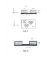
A Figura 1 exibe esquematicamente, na sua parte superior, uma seção através de um produto intermediário que pode servir de ponto de partida para o método de fabricação de acordo com a presente invenção. A parte inferior da Figura exibe uma vista superior sobre esse produto. O produto compreende um substrato plano 110, tal como uma placa de vidro ou plástico transparente, com uma camada de ânodos transparente 111 sobre ele (tal como ITO) . Além disso, duas pilhas localizadas estão dispostas sobre a camada de ânodos 111, em que as mencionadas pilhas compreendem uma camada eletroluminescente orgânica 120 e uma camada catódica 130 sobre ela. A camada de ânodos 111, a camada eletroluminescente orgânica 120 e a camada catódica 130 constituem "unidades funcionais", mais especificamente no presente unidades emissoras de luz LUI, LU2, LU3, que são dispostas sobre o substrato comum 110. Como exibe a vista superior da parte direita da Figura 1, as unidades emissoras de luz LUI, LU2 e LU3 podem ser moldadas livremente de acordo com as necessidades na sua aplicação pretendida. A forma das unidades emissoras de luz pode ser realizada, por exemplo, utilizando máscaras ou etapas de processo de corrosão de plasma.Figure 1 schematically shows, in its upper part, a section through an intermediate product that can serve as a starting point for the manufacturing method according to the present invention. The bottom part of the Figure shows a top view of this product. The product comprises a
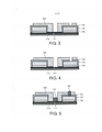
As etapas de processamento a seguir fornecem encapsulação de filme fino (TFE) do dispositivo de OLED da Figura 1. A Figura 2 exibe a primeira etapa neste particular, que é a deposição de uma camada de encapsulação inorgânica 140 (uma barreira de difusão de água), tal como SiN. Alternativamente, a TFE poderá começar com a deposição de uma camada orgânica, seguida pela camada inorgânica ilustrada.The following processing steps provide thin film encapsulation (TFE) of the OLED device of Figure 1. Figure 2 shows the first step in this particular, which is the deposition of an inorganic encapsulation layer 140 (a water diffusion barrier ), such as SiN. Alternatively, TFE may begin with the deposition of an organic layer, followed by the illustrated inorganic layer.
Segundo a Figura 3, isso é seguido pela deposição de uma camada orgânica 150, tal como um polímero com polímero com teor de água baixo ou inexistente. Para deposição estruturada da camada orgânica 150, pode ser utilizado um processo de impressão, tal como plotagem ou impressão a jato de tinta, ou um processo litográfico, tal como corrosão e exposição à luz (UV).According to Figure 3, this is followed by the deposition of an
Conforme exibido na Figura 4, a camada orgânica 150 pode ser utilizada como máscara para estruturar a camada inorgânica 140 abaixo e abrir contatos para a camada de ânodos 111 e a camada catódica 130 durante o processo de corrosão com plasma.As shown in Figure 4, the
A sequência de processo das Figuras 2 a 4 (deposição de camada inorgânica, deposição de camada orgânica, processo de corrosão) pode ser opcionalmente repetida diversas vezes (não exibido).The process sequence of Figures 2 to 4 (deposition of inorganic layer, deposition of organic layer, corrosion process) can optionally be repeated several times (not shown).
A Figura 5 exibe a etapa de processo seguinte (opcional), que é a aplicação de linhas de metais condutores 161 e 162 como barras terminais e/ou linhas de contato, tal como por meio de impressão ou evaporação. As barras de terminais podem ser também impressas no final da fabricação. Elas podem possuir formatos mais elaborados que as linhas de contato, tais como estruturas fechadas como uma grade.Figure 5 shows the next process step (optional), which is the application of
A Figura 6 exibe a aplicação de outra camada inorgânica 141 (tal como uma camada de SiN) e a Figura 7 exibe a aplicação de uma outra camada orgânica 151 como impressão de revestimento superior. Se necessário, pode seguir-se outra corrosão de SiN para abrir os pontos de contato CT para as linhas metálicas 161, 162, gerando o dispositivo de OLED final 100.Figure 6 shows the application of another inorganic layer 141 (such as a SiN layer) and Figure 7 shows the application of another
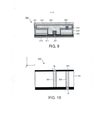
Nas Figuras 8, 9 e 10, um dispositivo de OLED alternativo 200 é exibido em vista em corte (Figuras 8 e 9) e uma vista superior (Figura 10) . Este dispositivo de OLED 200 compreende uma estrutura para embutir linhas de contato metálico e pode ser obtido por meio de etapas de processamento alternativas após o estágio da Figura 5. Particularmente, as linhas metálicas 261 e 262 podem ser completamente embutidas em primeiro lugar (além de em pontos de contato laterais CL) em uma camada de encapsulação orgânica 250, conforme ilustrado na vista em corte da Figura 8. Essa camada de encapsulação orgânica 250 pode ser adicionalmente coberta por uma camada inorgânica adicional 241 e uma camada orgânica adicional 251.In Figures 8, 9 and 10, an
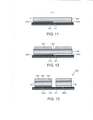
As Figuras 11 a 13 ilustram uma variante que pode substituir as etapas das Figuras 1 a 4. Segundo a Figura 10, esta variante começa com um substrato 310 que possui uma camada de ânodos (transparente) 311 e uma unidade emissora de luz LU no topo. A unidade emissora de luz LU é composta de duas fitas 320a e 320b de diferentes materiais eletroluminescentes orgânicos (por exemplo, emissores de vermelho e azul), que conduzem uma camada catódica 330 no topo. Naturalmente, poderão também ser utilizadas mais de duas fitas (com cores diferentes).Figures 11 to 13 illustrate a variant that can replace the steps in Figures 1 to 4. According to Figure 10, this variant starts with a
Segundo a Figura 12, uma camada inorgânica não estruturada 340 e uma camada orgânica estruturada 350 são depositadas em seguida sobre a unidade emissora de luz LU. Esta etapa é similar àquela exibida nas Figuras 2 e 3.According to Figure 12, an unstructured
Na etapa exibida na Figura 13, a camada inorgânica 340, a camada catódica 330 e as camadas eletroluminescentes orgânicas 320a, 320b foram corroídas, utilizando a camada orgânica superior 350 como máscara. Desta forma, diversos segmentos emissores de luz SI, S2 são gerados sobre o substrato 310. Naturalmente, podem também ser criadas aberturas adicionais desta forma (não exibida), particularmente para fornecer acesso às camadas de eletrodos. Além disso, o processamento adicional pode ocorrer conforme ilustrado nas Figuras 5 a 10, ou seja, por meio de conexão das camadas de eletrodos a linhas condutoras e de encapsulação dos segmentos SI, S2. Como resultado do procedimento descrito, é fornecida uma telha de iluminação de OLED segmentada 300.In the step shown in Figure 13, the
Em resumo, as realizações preferidas da presente invenção descritas acima compreendem as características a seguir: uma combinação de OLED de forma livre com encapsulação de filme fino de forma livre; contato com "lado traseiro" de um OLED encapsulado em filme fino (em que o termo "lado traseiro" designa o lado não emissor de luz do OLED); padrão de contato de forma livre por meio de corrosão com plasma de camadas inorgânicas; uso de intercamadas orgânicas como proteção contra a corrosão para as camadas inorgânicas; as camadas orgânicas ficam maiores em cada sequência de deposição, de forma a evitar vazamento lateral; fluxo de processo alternativo: encapsulação de filme fino mais confiável devido ao embutimento das linhas de contato na camada orgânica (ou seja, nenhum distúrbio da camada de SiN devido a extremidades etc.).In summary, the preferred embodiments of the present invention described above comprise the following characteristics: a combination of free-form OLED with free-form thin film encapsulation; contact with the "rear side" of an OLED encapsulated in thin film (where the term "rear side" designates the non-light emitting side of the OLED); free-form contact pattern by means of plasma corrosion of inorganic layers; use of organic interlayers as protection against corrosion for inorganic layers; the organic layers get bigger in each deposition sequence, in order to avoid lateral leakage; alternative process flow: more reliable thin film encapsulation due to the embedding of the contact lines in the organic layer (ie, no disturbance of the SiN layer due to ends etc.).
A presente invenção pode ser aplicada, por exemplo, em iluminação com OLED, fotovoltaicos orgânicos ou memórias orgânicas (MEMs).The present invention can be applied, for example, in lighting with OLED, organic photovoltaics or organic memories (MEMs).
Por fim, indica-se que, no presente pedido, a expressão "que compreende" não exclui outros elementos ou 5 etapas, "um” ou "uma" não exclui uma série e que um único processador ou outra unidade pode desempenhar as funções de diversos meios. A presente invenção reside em toda e qualquer função característica inovadora e toda e qualquer combinação de funções características. Além disso, os sinais de 10 referência nas reivindicações não deverão ser interpretados como limitadores do seu escopo.Finally, it is stated that, in the present application, the expression "which comprises" does not exclude other elements or 5 stages, "one" or "one" does not exclude a series and that a single processor or other unit can perform the functions of The present invention resides in each and every innovative characteristic function and any and all combination of characteristic functions In addition, the reference signs in the claims should not be interpreted as limiting its scope.
Claims (14)
Applications Claiming Priority (3)
| Application Number | Priority Date | Filing Date | Title |
|---|---|---|---|
| EP10187219.0 | 2010-10-12 | ||
| EP10187219 | 2010-10-12 | ||
| PCT/IB2011/054407 WO2012049594A1 (en) | 2010-10-12 | 2011-10-06 | Organic electronic device with encapsulation |
Publications (2)
| Publication Number | Publication Date |
|---|---|
| BR112013008571A2 BR112013008571A2 (en) | 2019-11-19 |
| BR112013008571B1 true BR112013008571B1 (en) | 2021-02-23 |
Family
ID=44860460
Family Applications (1)
| Application Number | Title | Priority Date | Filing Date |
|---|---|---|---|
| BR112013008571-1A BR112013008571B1 (en) | 2010-10-12 | 2011-10-06 | METHOD OF MANUFACTURING ORGANIC ELECTRONIC DEVICES |
Country Status (9)
| Country | Link |
|---|---|
| US (1) | US9219246B2 (en) |
| EP (1) | EP2628201B1 (en) |
| JP (1) | JP6014593B2 (en) |
| KR (1) | KR101843028B1 (en) |
| CN (1) | CN103155203B (en) |
| BR (1) | BR112013008571B1 (en) |
| RU (1) | RU2575938C2 (en) |
| TW (1) | TW201222914A (en) |
| WO (1) | WO2012049594A1 (en) |
Families Citing this family (12)
| Publication number | Priority date | Publication date | Assignee | Title |
|---|---|---|---|---|
| DE102012222772B4 (en) * | 2012-12-11 | 2021-09-16 | Pictiva Displays International Limited | Organic optoelectronic component |
| CN103904249B (en) * | 2012-12-25 | 2016-05-18 | 海洋王照明科技股份有限公司 | Organic electroluminescence device and preparation method thereof |
| KR102088203B1 (en) * | 2013-10-01 | 2020-03-12 | 엘지디스플레이 주식회사 | Organic light emitting diode display and manufacturing method thereof |
| DE102014101518A1 (en) * | 2014-02-07 | 2015-08-13 | Osram Oled Gmbh | Organic optoelectronic component and method for producing an organic optoelectronic component |
| FR3021460B1 (en) * | 2014-05-26 | 2017-03-10 | Astron Fiamm Safety | DEVICE COMPRISING AT LEAST TWO ORGANIC ELECTROLUMINESCENT DIODES |
| CN104241330B (en) | 2014-09-05 | 2017-05-03 | 京东方科技集团股份有限公司 | Organic light emitting diode display device and manufacturing method thereof |
| CN105206764A (en) * | 2015-08-20 | 2015-12-30 | 深圳市星火辉煌系统工程有限公司 | Sealing technology of OLED display device |
| US9812667B2 (en) | 2015-11-04 | 2017-11-07 | Microsoft Technology Licensing, Llc | Patterning of OLED display stacks |
| US10593908B2 (en) * | 2016-04-12 | 2020-03-17 | Lg Chem, Ltd. | Encapsulation film |
| CN109904341B (en) * | 2019-01-31 | 2020-08-04 | 武汉华星光电半导体显示技术有限公司 | O L ED display panel and preparation method thereof |
| CN110323358B (en) * | 2019-07-11 | 2021-12-24 | 京东方科技集团股份有限公司 | Light emitting diode, method of manufacturing the same, and light emitting device |
| CN110429064B (en) * | 2019-08-01 | 2020-11-10 | 武汉华星光电半导体显示技术有限公司 | Buffer structure, display panel and manufacturing method of buffer structure |
Family Cites Families (20)
| Publication number | Priority date | Publication date | Assignee | Title |
|---|---|---|---|---|
| JP3537591B2 (en) * | 1996-04-26 | 2004-06-14 | パイオニア株式会社 | Manufacturing method of organic EL display |
| US6274887B1 (en) * | 1998-11-02 | 2001-08-14 | Semiconductor Energy Laboratory Co., Ltd. | Semiconductor device and manufacturing method therefor |
| US6268695B1 (en) * | 1998-12-16 | 2001-07-31 | Battelle Memorial Institute | Environmental barrier material for organic light emitting device and method of making |
| BE1012802A3 (en) * | 1999-07-28 | 2001-03-06 | Cockerill Rech & Dev | Electroluminescent and device manufacturing method thereof. |
| TW546857B (en) * | 2001-07-03 | 2003-08-11 | Semiconductor Energy Lab | Light-emitting device, method of manufacturing a light-emitting device, and electronic equipment |
| JP3761843B2 (en) * | 2001-07-03 | 2006-03-29 | 株式会社半導体エネルギー研究所 | LIGHT EMITTING DEVICE AND ELECTRONIC DEVICE |
| JP3775499B2 (en) * | 2002-01-08 | 2006-05-17 | 株式会社リコー | Semiconductor device, manufacturing method thereof, and DC-DC converter |
| JP2004014447A (en) * | 2002-06-11 | 2004-01-15 | Sony Corp | Display device and manufacturing method therefor |
| AU2003256025A1 (en) * | 2002-10-07 | 2004-04-23 | Koninklijke Philips Electronics N.V. | Method for manufacturing a light emitting display |
| JP2006502539A (en) * | 2002-10-07 | 2006-01-19 | コーニンクレッカ フィリップス エレクトロニクス エヌ ヴィ | Manufacturing method of light emitting display |
| JP2005266616A (en) * | 2004-03-19 | 2005-09-29 | Hideki Matsumura | Optical display device and method for manufacturing the same |
| JP4708360B2 (en) * | 2004-10-29 | 2011-06-22 | パイオニア株式会社 | Organic electroluminescent display device and manufacturing method thereof |
| JP4696796B2 (en) * | 2005-09-07 | 2011-06-08 | 株式会社豊田自動織機 | Method for manufacturing organic electroluminescence device |
| JP2007080569A (en) * | 2005-09-12 | 2007-03-29 | Toyota Industries Corp | Method for manufacturing organic electroluminescence element |
| JP4795779B2 (en) * | 2005-11-09 | 2011-10-19 | 株式会社アルバック | Organic electroluminescence display panel |
| EP1804310B1 (en) * | 2005-12-30 | 2016-10-19 | Samsung Display Co., Ltd. | Organic light emiting device and method of manufacturing the same |
| JP2008071561A (en) * | 2006-09-13 | 2008-03-27 | Fuji Electric Holdings Co Ltd | Organic el element and manufacturing method of organic el element |
| JP2008270018A (en) * | 2007-04-23 | 2008-11-06 | Toyota Industries Corp | Manufacturing method of organic element sealing panel |
| EP2144290A1 (en) * | 2008-07-08 | 2010-01-13 | Nederlandse Organisatie voor toegepast- natuurwetenschappelijk onderzoek TNO | Electronic device and method of manufacturing the same |
| FR2936651B1 (en) * | 2008-09-30 | 2011-04-08 | Commissariat Energie Atomique | ORGANIC OPTOELECTRONIC DEVICE AND METHOD OF ENCAPSULATION |
-
2011
- 2011-10-06 BR BR112013008571-1A patent/BR112013008571B1/en active IP Right Grant
- 2011-10-06 CN CN201180049430.7A patent/CN103155203B/en active Active
- 2011-10-06 EP EP11773566.2A patent/EP2628201B1/en active Active
- 2011-10-06 RU RU2013121673/28A patent/RU2575938C2/en active
- 2011-10-06 JP JP2013533301A patent/JP6014593B2/en active Active
- 2011-10-06 KR KR1020137012212A patent/KR101843028B1/en active IP Right Grant
- 2011-10-06 WO PCT/IB2011/054407 patent/WO2012049594A1/en active Application Filing
- 2011-10-06 US US13/877,689 patent/US9219246B2/en active Active
- 2011-10-11 TW TW100136809A patent/TW201222914A/en unknown
Also Published As
| Publication number | Publication date |
|---|---|
| WO2012049594A1 (en) | 2012-04-19 |
| EP2628201A1 (en) | 2013-08-21 |
| KR101843028B1 (en) | 2018-05-14 |
| CN103155203B (en) | 2017-04-05 |
| CN103155203A (en) | 2013-06-12 |
| TW201222914A (en) | 2012-06-01 |
| RU2013121673A (en) | 2014-11-20 |
| RU2575938C2 (en) | 2016-02-27 |
| US9219246B2 (en) | 2015-12-22 |
| KR20130108388A (en) | 2013-10-02 |
| BR112013008571A2 (en) | 2019-11-19 |
| JP2013542569A (en) | 2013-11-21 |
| US20130217168A1 (en) | 2013-08-22 |
| JP6014593B2 (en) | 2016-10-25 |
| EP2628201B1 (en) | 2020-01-08 |
Similar Documents
| Publication | Publication Date | Title |
|---|---|---|
| BR112013008571B1 (en) | METHOD OF MANUFACTURING ORGANIC ELECTRONIC DEVICES | |
| JP7203763B2 (en) | DISPLAY SUBSTRATE AND MANUFACTURING METHOD THEREOF, DISPLAY DEVICE | |
| US10476029B2 (en) | Package structure of organic electroluminescent device and manufacturing method thereof, and display device | |
| US6952078B1 (en) | Encapsulation for organic LED device | |
| KR101727344B1 (en) | Encapsulated optoelectronic device and method for making the same | |
| JP5794915B2 (en) | Beam emitting device and method of manufacturing beam emitting device | |
| US20200203446A1 (en) | Display substrate and method of fabricating the same, and display device | |
| WO2016033931A1 (en) | Display panel and preparation method therefor, and display apparatus | |
| US7423375B2 (en) | Encapsulation for electroluminescent devices | |
| CN105374946B (en) | A kind of flexible display apparatus and preparation method thereof | |
| KR102105509B1 (en) | Encapsulation structure, display panel and manufacturing method thereof | |
| KR102612034B1 (en) | Flexible electronic device | |
| EP1317874A1 (en) | Patterning of electrodes in oled devices | |
| US10903444B2 (en) | OLED package substrate having a conductor attached to electrode on an array substrate | |
| EP2887397A1 (en) | Organic electroluminescence device and method for manufacturing the same | |
| US20150162564A1 (en) | Organic electroluminescence device | |
| KR20160083588A (en) | Organic light emitting display device and method for manufacturing thereof | |
| TW200427359A (en) | Organic electroluminescence display panel | |
| CN109686856A (en) | OLED device and preparation method thereof | |
| CN109148381B (en) | Array substrate, manufacturing method thereof, display panel and display device | |
| JP6817819B2 (en) | Organic EL element and manufacturing method of organic EL element | |
| CN108010941B (en) | Packaging structure and method for light-emitting element | |
| US20200235195A1 (en) | Display device, manufacturing method of display device, and exposure device | |
| CN109887974B (en) | Organic light emitting diode display and manufacturing method thereof | |
| US20230354648A1 (en) | Display device and method for manufacturing display device |
Legal Events
| Date | Code | Title | Description |
|---|---|---|---|
| B06F | Objections, documents and/or translations needed after an examination request according [chapter 6.6 patent gazette] | ||
| B25D | Requested change of name of applicant approved |
Owner name: KONINKLIJKE PHILIPS N.V. (NL) |
|
| B25G | Requested change of headquarter approved |
Owner name: KONINKLIJKE PHILIPS N.V. (NL) |
|
| B25A | Requested transfer of rights approved |
Owner name: BEIJING XIAOMI MOBILE SOFTWARE CO., LTD. (CN) |
|
| B06U | Preliminary requirement: requests with searches performed by other patent offices: procedure suspended [chapter 6.21 patent gazette] | ||
| B09A | Decision: intention to grant [chapter 9.1 patent gazette] | ||
| B16A | Patent or certificate of addition of invention granted [chapter 16.1 patent gazette] |
Free format text: PRAZO DE VALIDADE: 20 (VINTE) ANOS CONTADOS A PARTIR DE 06/10/2011, OBSERVADAS AS CONDICOES LEGAIS. |