KR20140039330A - Multiple bonding layers for thin-wafer handling - Google Patents
Multiple bonding layers for thin-wafer handling Download PDFInfo
- Publication number
- KR20140039330A KR20140039330A KR1020147003864A KR20147003864A KR20140039330A KR 20140039330 A KR20140039330 A KR 20140039330A KR 1020147003864 A KR1020147003864 A KR 1020147003864A KR 20147003864 A KR20147003864 A KR 20147003864A KR 20140039330 A KR20140039330 A KR 20140039330A
- Authority
- KR
- South Korea
- Prior art keywords
- layer
- bonding
- wafer
- substrate
- seconds
- Prior art date
Links
Images


Classifications
-
- H—ELECTRICITY
- H01—ELECTRIC ELEMENTS
- H01L—SEMICONDUCTOR DEVICES NOT COVERED BY CLASS H10
- H01L21/00—Processes or apparatus adapted for the manufacture or treatment of semiconductor or solid state devices or of parts thereof
- H01L21/67—Apparatus specially adapted for handling semiconductor or electric solid state devices during manufacture or treatment thereof; Apparatus specially adapted for handling wafers during manufacture or treatment of semiconductor or electric solid state devices or components ; Apparatus not specifically provided for elsewhere
- H01L21/683—Apparatus specially adapted for handling semiconductor or electric solid state devices during manufacture or treatment thereof; Apparatus specially adapted for handling wafers during manufacture or treatment of semiconductor or electric solid state devices or components ; Apparatus not specifically provided for elsewhere for supporting or gripping
- H01L21/6835—Apparatus specially adapted for handling semiconductor or electric solid state devices during manufacture or treatment thereof; Apparatus specially adapted for handling wafers during manufacture or treatment of semiconductor or electric solid state devices or components ; Apparatus not specifically provided for elsewhere for supporting or gripping using temporarily an auxiliary support
-
- B—PERFORMING OPERATIONS; TRANSPORTING
- B32—LAYERED PRODUCTS
- B32B—LAYERED PRODUCTS, i.e. PRODUCTS BUILT-UP OF STRATA OF FLAT OR NON-FLAT, e.g. CELLULAR OR HONEYCOMB, FORM
- B32B38/00—Ancillary operations in connection with laminating processes
- B32B38/0008—Electrical discharge treatment, e.g. corona, plasma treatment; wave energy or particle radiation
-
- B—PERFORMING OPERATIONS; TRANSPORTING
- B32—LAYERED PRODUCTS
- B32B—LAYERED PRODUCTS, i.e. PRODUCTS BUILT-UP OF STRATA OF FLAT OR NON-FLAT, e.g. CELLULAR OR HONEYCOMB, FORM
- B32B38/00—Ancillary operations in connection with laminating processes
- B32B38/10—Removing layers, or parts of layers, mechanically or chemically
-
- B—PERFORMING OPERATIONS; TRANSPORTING
- B32—LAYERED PRODUCTS
- B32B—LAYERED PRODUCTS, i.e. PRODUCTS BUILT-UP OF STRATA OF FLAT OR NON-FLAT, e.g. CELLULAR OR HONEYCOMB, FORM
- B32B43/00—Operations specially adapted for layered products and not otherwise provided for, e.g. repairing; Apparatus therefor
- B32B43/006—Delaminating
-
- H—ELECTRICITY
- H01—ELECTRIC ELEMENTS
- H01L—SEMICONDUCTOR DEVICES NOT COVERED BY CLASS H10
- H01L21/00—Processes or apparatus adapted for the manufacture or treatment of semiconductor or solid state devices or of parts thereof
- H01L21/02—Manufacture or treatment of semiconductor devices or of parts thereof
- H01L21/04—Manufacture or treatment of semiconductor devices or of parts thereof the devices having at least one potential-jump barrier or surface barrier, e.g. PN junction, depletion layer or carrier concentration layer
- H01L21/18—Manufacture or treatment of semiconductor devices or of parts thereof the devices having at least one potential-jump barrier or surface barrier, e.g. PN junction, depletion layer or carrier concentration layer the devices having semiconductor bodies comprising elements of Group IV of the Periodic System or AIIIBV compounds with or without impurities, e.g. doping materials
- H01L21/20—Deposition of semiconductor materials on a substrate, e.g. epitaxial growth solid phase epitaxy
- H01L21/2003—Deposition of semiconductor materials on a substrate, e.g. epitaxial growth solid phase epitaxy characterised by the substrate
- H01L21/2007—Bonding of semiconductor wafers to insulating substrates or to semiconducting substrates using an intermediate insulating layer
-
- H—ELECTRICITY
- H01—ELECTRIC ELEMENTS
- H01L—SEMICONDUCTOR DEVICES NOT COVERED BY CLASS H10
- H01L21/00—Processes or apparatus adapted for the manufacture or treatment of semiconductor or solid state devices or of parts thereof
- H01L21/67—Apparatus specially adapted for handling semiconductor or electric solid state devices during manufacture or treatment thereof; Apparatus specially adapted for handling wafers during manufacture or treatment of semiconductor or electric solid state devices or components ; Apparatus not specifically provided for elsewhere
- H01L21/683—Apparatus specially adapted for handling semiconductor or electric solid state devices during manufacture or treatment thereof; Apparatus specially adapted for handling wafers during manufacture or treatment of semiconductor or electric solid state devices or components ; Apparatus not specifically provided for elsewhere for supporting or gripping
- H01L21/6835—Apparatus specially adapted for handling semiconductor or electric solid state devices during manufacture or treatment thereof; Apparatus specially adapted for handling wafers during manufacture or treatment of semiconductor or electric solid state devices or components ; Apparatus not specifically provided for elsewhere for supporting or gripping using temporarily an auxiliary support
- H01L21/6836—Wafer tapes, e.g. grinding or dicing support tapes
-
- H—ELECTRICITY
- H01—ELECTRIC ELEMENTS
- H01L—SEMICONDUCTOR DEVICES NOT COVERED BY CLASS H10
- H01L24/00—Arrangements for connecting or disconnecting semiconductor or solid-state bodies; Methods or apparatus related thereto
- H01L24/80—Methods for connecting semiconductor or other solid state bodies using means for bonding being attached to, or being formed on, the surface to be connected
- H01L24/83—Methods for connecting semiconductor or other solid state bodies using means for bonding being attached to, or being formed on, the surface to be connected using a layer connector
-
- H—ELECTRICITY
- H01—ELECTRIC ELEMENTS
- H01L—SEMICONDUCTOR DEVICES NOT COVERED BY CLASS H10
- H01L2221/00—Processes or apparatus adapted for the manufacture or treatment of semiconductor or solid state devices or of parts thereof covered by H01L21/00
- H01L2221/67—Apparatus for handling semiconductor or electric solid state devices during manufacture or treatment thereof; Apparatus for handling wafers during manufacture or treatment of semiconductor or electric solid state devices or components; Apparatus not specifically provided for elsewhere
- H01L2221/683—Apparatus for handling semiconductor or electric solid state devices during manufacture or treatment thereof; Apparatus for handling wafers during manufacture or treatment of semiconductor or electric solid state devices or components; Apparatus not specifically provided for elsewhere for supporting or gripping
- H01L2221/68304—Apparatus for handling semiconductor or electric solid state devices during manufacture or treatment thereof; Apparatus for handling wafers during manufacture or treatment of semiconductor or electric solid state devices or components; Apparatus not specifically provided for elsewhere for supporting or gripping using temporarily an auxiliary support
- H01L2221/68318—Auxiliary support including means facilitating the separation of a device or wafer from the auxiliary support
-
- H—ELECTRICITY
- H01—ELECTRIC ELEMENTS
- H01L—SEMICONDUCTOR DEVICES NOT COVERED BY CLASS H10
- H01L2221/00—Processes or apparatus adapted for the manufacture or treatment of semiconductor or solid state devices or of parts thereof covered by H01L21/00
- H01L2221/67—Apparatus for handling semiconductor or electric solid state devices during manufacture or treatment thereof; Apparatus for handling wafers during manufacture or treatment of semiconductor or electric solid state devices or components; Apparatus not specifically provided for elsewhere
- H01L2221/683—Apparatus for handling semiconductor or electric solid state devices during manufacture or treatment thereof; Apparatus for handling wafers during manufacture or treatment of semiconductor or electric solid state devices or components; Apparatus not specifically provided for elsewhere for supporting or gripping
- H01L2221/68304—Apparatus for handling semiconductor or electric solid state devices during manufacture or treatment thereof; Apparatus for handling wafers during manufacture or treatment of semiconductor or electric solid state devices or components; Apparatus not specifically provided for elsewhere for supporting or gripping using temporarily an auxiliary support
- H01L2221/68327—Apparatus for handling semiconductor or electric solid state devices during manufacture or treatment thereof; Apparatus for handling wafers during manufacture or treatment of semiconductor or electric solid state devices or components; Apparatus not specifically provided for elsewhere for supporting or gripping using temporarily an auxiliary support used during dicing or grinding
-
- H—ELECTRICITY
- H01—ELECTRIC ELEMENTS
- H01L—SEMICONDUCTOR DEVICES NOT COVERED BY CLASS H10
- H01L2221/00—Processes or apparatus adapted for the manufacture or treatment of semiconductor or solid state devices or of parts thereof covered by H01L21/00
- H01L2221/67—Apparatus for handling semiconductor or electric solid state devices during manufacture or treatment thereof; Apparatus for handling wafers during manufacture or treatment of semiconductor or electric solid state devices or components; Apparatus not specifically provided for elsewhere
- H01L2221/683—Apparatus for handling semiconductor or electric solid state devices during manufacture or treatment thereof; Apparatus for handling wafers during manufacture or treatment of semiconductor or electric solid state devices or components; Apparatus not specifically provided for elsewhere for supporting or gripping
- H01L2221/68304—Apparatus for handling semiconductor or electric solid state devices during manufacture or treatment thereof; Apparatus for handling wafers during manufacture or treatment of semiconductor or electric solid state devices or components; Apparatus not specifically provided for elsewhere for supporting or gripping using temporarily an auxiliary support
- H01L2221/6834—Apparatus for handling semiconductor or electric solid state devices during manufacture or treatment thereof; Apparatus for handling wafers during manufacture or treatment of semiconductor or electric solid state devices or components; Apparatus not specifically provided for elsewhere for supporting or gripping using temporarily an auxiliary support used to protect an active side of a device or wafer
-
- H—ELECTRICITY
- H01—ELECTRIC ELEMENTS
- H01L—SEMICONDUCTOR DEVICES NOT COVERED BY CLASS H10
- H01L2221/00—Processes or apparatus adapted for the manufacture or treatment of semiconductor or solid state devices or of parts thereof covered by H01L21/00
- H01L2221/67—Apparatus for handling semiconductor or electric solid state devices during manufacture or treatment thereof; Apparatus for handling wafers during manufacture or treatment of semiconductor or electric solid state devices or components; Apparatus not specifically provided for elsewhere
- H01L2221/683—Apparatus for handling semiconductor or electric solid state devices during manufacture or treatment thereof; Apparatus for handling wafers during manufacture or treatment of semiconductor or electric solid state devices or components; Apparatus not specifically provided for elsewhere for supporting or gripping
- H01L2221/68304—Apparatus for handling semiconductor or electric solid state devices during manufacture or treatment thereof; Apparatus for handling wafers during manufacture or treatment of semiconductor or electric solid state devices or components; Apparatus not specifically provided for elsewhere for supporting or gripping using temporarily an auxiliary support
- H01L2221/68381—Details of chemical or physical process used for separating the auxiliary support from a device or wafer
-
- H—ELECTRICITY
- H01—ELECTRIC ELEMENTS
- H01L—SEMICONDUCTOR DEVICES NOT COVERED BY CLASS H10
- H01L2924/00—Indexing scheme for arrangements or methods for connecting or disconnecting semiconductor or solid-state bodies as covered by H01L24/00
- H01L2924/10—Details of semiconductor or other solid state devices to be connected
- H01L2924/11—Device type
- H01L2924/12—Passive devices, e.g. 2 terminal devices
- H01L2924/1204—Optical Diode
- H01L2924/12041—LED
-
- H—ELECTRICITY
- H01—ELECTRIC ELEMENTS
- H01L—SEMICONDUCTOR DEVICES NOT COVERED BY CLASS H10
- H01L2924/00—Indexing scheme for arrangements or methods for connecting or disconnecting semiconductor or solid-state bodies as covered by H01L24/00
- H01L2924/10—Details of semiconductor or other solid state devices to be connected
- H01L2924/11—Device type
- H01L2924/12—Passive devices, e.g. 2 terminal devices
- H01L2924/1204—Optical Diode
- H01L2924/12042—LASER
-
- H—ELECTRICITY
- H01—ELECTRIC ELEMENTS
- H01L—SEMICONDUCTOR DEVICES NOT COVERED BY CLASS H10
- H01L2924/00—Indexing scheme for arrangements or methods for connecting or disconnecting semiconductor or solid-state bodies as covered by H01L24/00
- H01L2924/10—Details of semiconductor or other solid state devices to be connected
- H01L2924/11—Device type
- H01L2924/14—Integrated circuits
-
- H—ELECTRICITY
- H01—ELECTRIC ELEMENTS
- H01L—SEMICONDUCTOR DEVICES NOT COVERED BY CLASS H10
- H01L2924/00—Indexing scheme for arrangements or methods for connecting or disconnecting semiconductor or solid-state bodies as covered by H01L24/00
- H01L2924/10—Details of semiconductor or other solid state devices to be connected
- H01L2924/146—Mixed devices
- H01L2924/1461—MEMS
-
- H—ELECTRICITY
- H01—ELECTRIC ELEMENTS
- H01L—SEMICONDUCTOR DEVICES NOT COVERED BY CLASS H10
- H01L2924/00—Indexing scheme for arrangements or methods for connecting or disconnecting semiconductor or solid-state bodies as covered by H01L24/00
- H01L2924/30—Technical effects
- H01L2924/35—Mechanical effects
- H01L2924/351—Thermal stress
-
- Y—GENERAL TAGGING OF NEW TECHNOLOGICAL DEVELOPMENTS; GENERAL TAGGING OF CROSS-SECTIONAL TECHNOLOGIES SPANNING OVER SEVERAL SECTIONS OF THE IPC; TECHNICAL SUBJECTS COVERED BY FORMER USPC CROSS-REFERENCE ART COLLECTIONS [XRACs] AND DIGESTS
- Y10—TECHNICAL SUBJECTS COVERED BY FORMER USPC
- Y10T—TECHNICAL SUBJECTS COVERED BY FORMER US CLASSIFICATION
- Y10T156/00—Adhesive bonding and miscellaneous chemical manufacture
- Y10T156/10—Methods of surface bonding and/or assembly therefor
-
- Y—GENERAL TAGGING OF NEW TECHNOLOGICAL DEVELOPMENTS; GENERAL TAGGING OF CROSS-SECTIONAL TECHNOLOGIES SPANNING OVER SEVERAL SECTIONS OF THE IPC; TECHNICAL SUBJECTS COVERED BY FORMER USPC CROSS-REFERENCE ART COLLECTIONS [XRACs] AND DIGESTS
- Y10—TECHNICAL SUBJECTS COVERED BY FORMER USPC
- Y10T—TECHNICAL SUBJECTS COVERED BY FORMER US CLASSIFICATION
- Y10T156/00—Adhesive bonding and miscellaneous chemical manufacture
- Y10T156/11—Methods of delaminating, per se; i.e., separating at bonding face
- Y10T156/1126—Using direct fluid current against work during delaminating
-
- Y—GENERAL TAGGING OF NEW TECHNOLOGICAL DEVELOPMENTS; GENERAL TAGGING OF CROSS-SECTIONAL TECHNOLOGIES SPANNING OVER SEVERAL SECTIONS OF THE IPC; TECHNICAL SUBJECTS COVERED BY FORMER USPC CROSS-REFERENCE ART COLLECTIONS [XRACs] AND DIGESTS
- Y10—TECHNICAL SUBJECTS COVERED BY FORMER USPC
- Y10T—TECHNICAL SUBJECTS COVERED BY FORMER US CLASSIFICATION
- Y10T428/00—Stock material or miscellaneous articles
- Y10T428/24—Structurally defined web or sheet [e.g., overall dimension, etc.]
- Y10T428/24942—Structurally defined web or sheet [e.g., overall dimension, etc.] including components having same physical characteristic in differing degree
-
- Y—GENERAL TAGGING OF NEW TECHNOLOGICAL DEVELOPMENTS; GENERAL TAGGING OF CROSS-SECTIONAL TECHNOLOGIES SPANNING OVER SEVERAL SECTIONS OF THE IPC; TECHNICAL SUBJECTS COVERED BY FORMER USPC CROSS-REFERENCE ART COLLECTIONS [XRACs] AND DIGESTS
- Y10—TECHNICAL SUBJECTS COVERED BY FORMER USPC
- Y10T—TECHNICAL SUBJECTS COVERED BY FORMER US CLASSIFICATION
- Y10T428/00—Stock material or miscellaneous articles
- Y10T428/26—Web or sheet containing structurally defined element or component, the element or component having a specified physical dimension
-
- Y—GENERAL TAGGING OF NEW TECHNOLOGICAL DEVELOPMENTS; GENERAL TAGGING OF CROSS-SECTIONAL TECHNOLOGIES SPANNING OVER SEVERAL SECTIONS OF THE IPC; TECHNICAL SUBJECTS COVERED BY FORMER USPC CROSS-REFERENCE ART COLLECTIONS [XRACs] AND DIGESTS
- Y10—TECHNICAL SUBJECTS COVERED BY FORMER USPC
- Y10T—TECHNICAL SUBJECTS COVERED BY FORMER US CLASSIFICATION
- Y10T428/00—Stock material or miscellaneous articles
- Y10T428/31504—Composite [nonstructural laminate]
- Y10T428/31511—Of epoxy ether
-
- Y—GENERAL TAGGING OF NEW TECHNOLOGICAL DEVELOPMENTS; GENERAL TAGGING OF CROSS-SECTIONAL TECHNOLOGIES SPANNING OVER SEVERAL SECTIONS OF THE IPC; TECHNICAL SUBJECTS COVERED BY FORMER USPC CROSS-REFERENCE ART COLLECTIONS [XRACs] AND DIGESTS
- Y10—TECHNICAL SUBJECTS COVERED BY FORMER USPC
- Y10T—TECHNICAL SUBJECTS COVERED BY FORMER US CLASSIFICATION
- Y10T428/00—Stock material or miscellaneous articles
- Y10T428/31504—Composite [nonstructural laminate]
- Y10T428/31551—Of polyamidoester [polyurethane, polyisocyanate, polycarbamate, etc.]
-
- Y—GENERAL TAGGING OF NEW TECHNOLOGICAL DEVELOPMENTS; GENERAL TAGGING OF CROSS-SECTIONAL TECHNOLOGIES SPANNING OVER SEVERAL SECTIONS OF THE IPC; TECHNICAL SUBJECTS COVERED BY FORMER USPC CROSS-REFERENCE ART COLLECTIONS [XRACs] AND DIGESTS
- Y10—TECHNICAL SUBJECTS COVERED BY FORMER USPC
- Y10T—TECHNICAL SUBJECTS COVERED BY FORMER US CLASSIFICATION
- Y10T428/00—Stock material or miscellaneous articles
- Y10T428/31504—Composite [nonstructural laminate]
- Y10T428/31652—Of asbestos
- Y10T428/31663—As siloxane, silicone or silane
-
- Y—GENERAL TAGGING OF NEW TECHNOLOGICAL DEVELOPMENTS; GENERAL TAGGING OF CROSS-SECTIONAL TECHNOLOGIES SPANNING OVER SEVERAL SECTIONS OF THE IPC; TECHNICAL SUBJECTS COVERED BY FORMER USPC CROSS-REFERENCE ART COLLECTIONS [XRACs] AND DIGESTS
- Y10—TECHNICAL SUBJECTS COVERED BY FORMER USPC
- Y10T—TECHNICAL SUBJECTS COVERED BY FORMER US CLASSIFICATION
- Y10T428/00—Stock material or miscellaneous articles
- Y10T428/31504—Composite [nonstructural laminate]
- Y10T428/31721—Of polyimide
-
- Y—GENERAL TAGGING OF NEW TECHNOLOGICAL DEVELOPMENTS; GENERAL TAGGING OF CROSS-SECTIONAL TECHNOLOGIES SPANNING OVER SEVERAL SECTIONS OF THE IPC; TECHNICAL SUBJECTS COVERED BY FORMER USPC CROSS-REFERENCE ART COLLECTIONS [XRACs] AND DIGESTS
- Y10—TECHNICAL SUBJECTS COVERED BY FORMER USPC
- Y10T—TECHNICAL SUBJECTS COVERED BY FORMER US CLASSIFICATION
- Y10T428/00—Stock material or miscellaneous articles
- Y10T428/31504—Composite [nonstructural laminate]
- Y10T428/31725—Of polyamide
-
- Y—GENERAL TAGGING OF NEW TECHNOLOGICAL DEVELOPMENTS; GENERAL TAGGING OF CROSS-SECTIONAL TECHNOLOGIES SPANNING OVER SEVERAL SECTIONS OF THE IPC; TECHNICAL SUBJECTS COVERED BY FORMER USPC CROSS-REFERENCE ART COLLECTIONS [XRACs] AND DIGESTS
- Y10—TECHNICAL SUBJECTS COVERED BY FORMER USPC
- Y10T—TECHNICAL SUBJECTS COVERED BY FORMER US CLASSIFICATION
- Y10T428/00—Stock material or miscellaneous articles
- Y10T428/31504—Composite [nonstructural laminate]
- Y10T428/31855—Of addition polymer from unsaturated monomers
- Y10T428/31935—Ester, halide or nitrile of addition polymer
-
- Y—GENERAL TAGGING OF NEW TECHNOLOGICAL DEVELOPMENTS; GENERAL TAGGING OF CROSS-SECTIONAL TECHNOLOGIES SPANNING OVER SEVERAL SECTIONS OF THE IPC; TECHNICAL SUBJECTS COVERED BY FORMER USPC CROSS-REFERENCE ART COLLECTIONS [XRACs] AND DIGESTS
- Y10—TECHNICAL SUBJECTS COVERED BY FORMER USPC
- Y10T—TECHNICAL SUBJECTS COVERED BY FORMER US CLASSIFICATION
- Y10T428/00—Stock material or miscellaneous articles
- Y10T428/31504—Composite [nonstructural laminate]
- Y10T428/31855—Of addition polymer from unsaturated monomers
- Y10T428/31938—Polymer of monoethylenically unsaturated hydrocarbon
Abstract
반도체 기판들을 임시로 접합하는 다중 본딩 층 스킴이 제공된다. 본 발명의 본딩 스킴에서, 층들 중 적어도 하나가 반도체 기판과 직접 접촉하며, 스킴 내 적어도 2개의 층은 서로 직접 접촉한다. 본 발명은 다층 구조물 내 서로 다른 층들이 특정 기능을 수행함에 따른 몇 가지 공정 옵션을 제공한다. 더 중요하게는, 이는 열적 안정성을 더 높이고, 거친(harsh) 후면 공정 단계와의 호환성을 더 높이며, 캡슐화에 의해 웨이퍼의 전면 상의 범프를 보호하고, 디본딩 공정의 응력을 더 낮추며, 전면 상의 결함을 감소시킴으로써, 박형 웨이퍼 핸들링 솔루션의 성능을 개선할 것이다. A multiple bonding layer scheme is provided for temporarily bonding semiconductor substrates. In the bonding scheme of the present invention, at least one of the layers is in direct contact with the semiconductor substrate and at least two layers in the scheme are in direct contact with each other. The present invention provides several process options as the different layers in the multilayer structure perform specific functions. More importantly, this results in higher thermal stability, greater compatibility with harsh backside processing steps, encapsulation to protect bumps on the front side of the wafer, lower stresses in the debonding process, and defects on the front side. By reducing this, the performance of the thin wafer handling solution will be improved.
Description
발명의 분야Field of invention
본 발명은 넓게는, 다중 층 본딩 시스템을 이용하는 신규한 임시 웨이퍼 본딩 방법에 관한 것이다. 본 발명의 방법은 웨이퍼 박층화(thinning) 공정 및 그 밖의 다른 후면 공정 동안 캐리어 기판 상에서 소자 웨이퍼를 지지할 수 있다. The present invention broadly relates to a novel temporary wafer bonding method using a multilayer bonding system. The method of the present invention may support device wafers on a carrier substrate during wafer thinning processes and other backside processes.
배경 기술의 설명Description of Background Art
집적 회로, 전력 반도체(power semiconductor), 발광 다이오드, 광자 회로(photonic circuit), 마이크로전자기계 시스템(MEMS: microelectromechanical system), 내장형 수동 어레이(embedded passive array), 패키징 인터포저(packaging interposer), 및 그 밖의 다른 실리콘계 및 화합물 반도체계 마이크로소자가 집합적으로 지름이 1-12인치인 웨이퍼 기판 상에서 어레이로 생산된다. 그 후, 상기 소자는 개별 소자 또는 다이로 분리되며, 상기 개별 소자 또는 다이는 패키징되어, 가령, 인쇄 배선 기판과의 인터커넥션에 의해, 거시적 환경과의 실제 인터페이싱을 가능하게 한다. 여전히 웨이퍼 어레이의 일부분이면서 다이 상에 또는 다이 부근에 소자 패키지를 구성하는 것이 점점 더 대중이 되고 있다. 이러한 실시는, 웨이퍼-레벨 패키징이라고 일컬어지며, 전체 패키징 비용을 낮추며, 일반적으로 실제 소자보다 수 배 더 큰 외부 치수를 갖는 종래 패키지를 이용하는 경우보다, 소자와 그 마이크로전자 환경 사이에 더 높은 인터커넥션 밀도가 얻어지게 한다.Integrated circuits, power semiconductors, light emitting diodes, photonic circuits, microelectromechanical systems (MEMS), embedded passive arrays, packaging interposers, and their Other silicon- and compound semiconductor-based microdevices outside are collectively produced in arrays on wafer substrates 1-12 inches in diameter. The devices are then separated into individual devices or dies, which are packaged to enable actual interfacing with the macroscopic environment, for example by interconnection with a printed wiring board. It is increasingly popular to configure device packages on or near the die while still being part of a wafer array. This practice, referred to as wafer-level packaging, lowers the overall packaging cost and generally results in higher interconnection between the device and its microelectronic environment than with conventional packages having external dimensions that are many times larger than actual devices. Allow density to be obtained.
지금까지, 인터커넥션 방식은 2개의 차원으로 한정되는 것이 일반적이었다. 즉, 소자와 상기 소자가 장착되는 대응 기판 또는 패키징 표면 간의 전기적 연결이 수평, 즉, x-y 평면으로 배치됨을 의미한다. 현재, 마이크로전자 산업에서, 소자를 수직으로, 즉, z-방향으로, 적층하고 인터커넥팅함으로써 소자 인터커넥션 밀도의 상당한 증가 및 이에 대응하는 신호 딜레이의 감소(전기 연결점들 간의 거리의 단축의 결과)가 얻어질 수 있음이 발견됐다. 소자 적층에 대한 다음의 두 가지 일반적인 요건이 있다: (1) 후면에서 소자를 웨이퍼 관통 방향으로 박층화하기, 및 (2) 그 후, 소자의 후면에서 종료되는 웨이퍼 관통 전기 연결을 형성하기(흔히, 관통형 실리콘 비아(TSV: through-silicon-vias)). 이를 위해, 소자가 적층된 구성으로 패키징되지 않을 때, 반도체 소자 박층화가, 컴팩트한 전자 제품, 가령, 셀룰러 전화기의 경우, 방열을 촉진하고, 훨씬 더 작은 폼 팩터(form factor)가 얻어질 수 있게 하기 때문에, 현재의 표준 실시법이 됐다. Until now, the interconnection scheme has generally been limited to two dimensions. That is, the electrical connection between the device and the corresponding substrate or packaging surface on which it is mounted is arranged horizontally, ie in the x-y plane. Currently, in the microelectronics industry, significant increases in device interconnect density and corresponding signal delays by stacking and interconnecting devices vertically, ie in the z-direction, as a result of shortening the distance between electrical connection points It was found that can be obtained. There are two general requirements for device stacking: (1) thinning the device in the wafer through direction at the backside, and (2) then forming a through-wafer electrical connection that terminates at the backside of the device (often , Through-silicon-vias (TSV). To this end, when the device is not packaged in a stacked configuration, semiconductor device thinning facilitates heat dissipation and enables a much smaller form factor to be obtained in compact electronics, such as cellular telephones. This is the current standard practice.
특히, 반도체 소자 또는 상기 반도체 소자가 위치하는 대응 패키지가 적층될 때, 반도체 소자의 프로파일(profile)을 감조시키기 위해, 그리고 소자의 후면 상의 전기 연결의 형성을 단순화시키기 위해, 100마이크론 미만으로 반도체 소자를 박층화하는 데에 대한 관심이 높아지고 있다. 고 체적 집적 회로 제품에서 사용되는 실리콘 웨이퍼는 통상적으로 200 또는 300mm 지름을 가지며, 약 750 마이크론의 웨이퍼 관통 두께를 가진다. 박층화 없이, 연결을 웨이퍼를 관통시킴으로써 전면 회로와 연결되는 후면 전기 접촉부를 형성하는 것은 거의 불가능할 것이다. 기계 연삭(후면 연삭(back-grinding)) 및 연마(polishing)뿐 아니라 화학적 에칭을 기반으로 하는 반도체-등급 실리콘 및 화합물 반도체에 대한 고효율 박층화 공정이 현재 상업적으로 사용되고 있다. 이들 공정에 의해, 웨이퍼 횡단(cross-wafer) 두께 균일성에 대한 정교한 제어를 유지하면서, 소자 웨이퍼 두께가 수 분 내에 100마이크론 미만으로 감소될 수 있다. In particular, when a semiconductor device or a corresponding package in which the semiconductor device is located is stacked, in order to reduce the profile of the semiconductor device and to simplify the formation of electrical connections on the back side of the device, the semiconductor device is less than 100 microns. There is a growing interest in thinning. Silicon wafers used in high volume integrated circuit products typically have a 200 or 300 mm diameter and have a wafer through thickness of about 750 microns. Without thinning, it would be nearly impossible to form a backside electrical contact to the front circuit by penetrating the wafer through the connection. High efficiency thinning processes for semiconductor-grade silicon and compound semiconductors based on mechanical etching (back-grinding) and polishing as well as chemical etching are currently commercially available. By these processes, the device wafer thickness can be reduced to less than 100 microns in minutes while maintaining fine control over wafer cross-wafer thickness uniformity.
100마이크론 미만으로 박층화된 소자 웨이퍼, 및 특히, 60마이크론 미만으로 박층화된 소자 웨이퍼는 극도로 부서지기 쉬우며, 균열과 파손을 막기 위해 그들의 전체 치수에서 지지되어야 한다. 초박(ultra-thin) 소자 웨이퍼를 이송하기 위해 다양한 웨이퍼 완드(wand) 및 척(chuck)이 개발되었지만, 화학-기계 연마(CMP), 리소그래피, 에칭, 증착, 어닐링, 및 세정 단계를 포함하는 후면 연삭 및 TSV-형성 공정 동안 웨이퍼를 지지하기 위한 방식에 대한 문제가 여전히 존재하는데, 왜냐하면 소자 웨이퍼가 박층화되는 중에 또는 박층화 후에, 상기 단계들이 높은 열적 및 기계적 응력을 소자 웨이퍼에 부가하기 때문이다. 초박 웨이퍼 핸들링에 대한 선호되는 방식은 폴리머 접착제를 이용해 전체 두께(full-thickness) 소자 웨이퍼를 뒤집어서 강성 캐리어에 장착하는 것을 포함한다. 그 후, 후면에서부터 박층화되고 가공된다. 그 후, 후면 가공이 완료된 후 열적, 열기계적, 또는 화학적 공정에 의해 완전 가공된 초박 웨이퍼가 캐리어로부터 제거되거나 디본딩(debond)된다.Device wafers thinned to less than 100 microns, and in particular device wafers thinned to less than 60 microns, are extremely brittle and must be supported in their overall dimensions to prevent cracking and breakage. Although various wafer wands and chucks have been developed for transferring ultra-thin device wafers, the backside includes chemical-mechanical polishing (CMP), lithography, etching, deposition, annealing, and cleaning steps. There is still a problem with the way to support the wafer during the grinding and TSV-forming process, since the steps add high thermal and mechanical stress to the device wafer while or after the device wafer is thinned. . Preferred approaches for ultra-thin wafer handling include inverting the full-thickness device wafer with a polymer adhesive and mounting it on a rigid carrier. Then, it is laminated and processed from the rear side. Thereafter, after the backside processing is completed, the ultrathin wafer, which is fully processed by a thermal, thermomechanical, or chemical process, is removed or debonded from the carrier.
일반적인 캐리어 물질은 실리콘(가령, 블랭크 소자 웨이퍼), 소다 석회 유리, 붕규산 유리, 사파이어, 및 다양한 금속 및 세라믹이 있다. 상기 캐리어는 정사각형 또는 직사각형일 수 있지만, 더 흔히는, 둥근형일 수 있고, 소자 웨이퍼와 일치하는 크기를 가져서, 본딩된 조립체가 종래의 공정 툴 및 카세트에서 취급될 수 있도록 할 수 있다. 이따금, 분리(release)를 위한 수단으로서 폴리머 접착제를 용해 또는 분해하기 위한 액체 화학제가 사용될 때 디본딩 공정의 속도를 높이기 위해, 캐리어는 천공가공(perforate)된다. 일반적으로 임시 웨이퍼 본딩을 위해 사용되는 폴리머 접착제는 용액으로부터의 스핀 코팅 또는 분사 코팅에 의해 또는 건식-필름 테이프로서 라미네이팅함으로써 도포된다. 스핀-도포 및 분사-도포된 접착제는 테이프가 제공할 수 있는 것보다 더 높은 두께 균일도(thickness uniformity)를 갖는 코팅을 형성하기 때문에 점점 더 선호되고 있다. 높은 두께 균일도일수록 박층화 이후 웨이퍼 횡단 두께 균일도에 대한 우수한 제어를 의미한다. 폴리머 접착제는 소자 웨이퍼와 캐리어에게 높은 본딩 강도(bonding strength)를 제공한다. Common carrier materials are silicon (eg, blank device wafers), soda lime glass, borosilicate glass, sapphire, and various metals and ceramics. The carrier may be square or rectangular, but more often it may be round and have a size consistent with the device wafer so that the bonded assembly can be handled in conventional process tools and cassettes. Occasionally, the carrier is perforated to speed up the debonding process when liquid chemicals are used to dissolve or dissolve the polymer adhesive as a means for release. Polymer adhesives generally used for temporary wafer bonding are applied by spin coating or spray coating from solution or by laminating as dry-film tape. Spin- and spray-coated adhesives are increasingly preferred because they form a coating with a higher thickness uniformity than the tape can provide. Higher thickness uniformity means better control of wafer thickness uniformity after thinning. Polymer adhesives provide high bonding strength for device wafers and carriers.
요구되는 두께 및 코팅 평탄도(coating planarity)(평탄한 정도)에 따라 폴리머 접착제는 소자 웨이퍼, 캐리어, 또는 둘 모두로 스핀-도포될 수 있다. 폴리머 접착제 층으로부터 코팅 용매 모두를 제거하기 위해 코팅된 웨이퍼가 베이킹된다. 그 후 코팅된 웨이퍼 및 캐리어가 본딩되기 위해 가열된 기계 프레스에 접촉하도록 배치된다. 접착제가 유동하고 소자 웨이퍼 구조 특징부 내부를 충전(fill)하며, 소자 웨이퍼 및 캐리어 표면의 모든 영역과의 친밀한 접촉을 이루도록 충분한 온도와 압력이 가해진다. Depending on the required thickness and coating planarity (flatness), the polymer adhesive can be spin-coated to the device wafer, carrier, or both. The coated wafer is baked to remove all of the coating solvent from the polymer adhesive layer. The coated wafer and carrier are then placed in contact with the heated mechanical press for bonding. Sufficient temperature and pressure are applied to allow the adhesive to flow and to fill the interior of the device wafer structural features and to make intimate contact with all areas of the device wafer and carrier surface.
후면 공정 이후 캐리어로부터 소자 웨이퍼를 디본딩하는 것이 다음의 네 가지 방식 중 하나로 수행되는 것이 일반적이다:It is common to debond the device wafer from the carrier after the backside process in one of four ways:
(1) 화학적 방식 - 폴리머 접착제를 용해 또는 분해하기 위해 용매 또는 화학제에 본딩된 웨이퍼 스택을 침지시키거나 상기 용매 또는 화학제를 상기 본딩된 웨이퍼 스택에 분사한다.(1) Chemical Mode-Immerse a wafer stack bonded to a solvent or chemical to dissolve or dissolve a polymer adhesive, or spray the solvent or chemical onto the bonded wafer stack.
(2) 광-분해(Photo-Decomposition) - 캐리어에 접하는 접착제 경계 층을 광-분해하기 위해 광원이, 투명 캐리어를 통해, 본딩된 웨이퍼 스택을 조사(irradiate)한다. 그 후 캐리어가 스택으로부터 분리될 수 있고, 폴리머 접착제의 잔여물이 척상에 고정된 소자 웨이퍼로부터 박리(peel)된다. (2) Photo-Decomposition—The light source irradiates the bonded wafer stack through the transparent carrier to photo-decompose the adhesive boundary layer in contact with the carrier. The carrier can then be separated from the stack and the remainder of the polymer adhesive is peeled from the device wafer fixed on the chuck.
(3) 열-기계적 방식 - 폴리머 접착제의 연화점 이상으로 본딩된 웨이퍼 스택이 가열되고, 그 후 소자 웨이퍼는 전체-웨이퍼 고정 척으로 지지되어 있는 캐리어로부터 미끄러지거나 당겨진다. (3) Thermo-mechanical Approach—The bonded wafer stack is heated above the softening point of the polymer adhesive, after which the device wafer is slid or pulled from the carrier supported by the full-wafer fixation chuck.
(4) 열 분해 - 폴리머 접착제의 분해 온도 이상으로 본딩된 웨이퍼 스택이 가열되며, 이로써, 소자 웨이퍼와 캐리어의 접착력이 휘발되고 상실되게 된다. (4) Pyrolysis—The wafer stack bonded above the decomposition temperature of the polymer adhesive is heated, thereby causing the adhesion between the device wafer and the carrier to be volatilized and lost.
이들 디본딩 방법 각각은 제조 환경에서 사용되는 것을 심각하게 제한하는 단점을 가진다. 예를 들면, 폴리머 접착제를 용해함으로써 이뤄지는 화학적 디본딩은 느린 공정인데, 왜냐하면 분리를 일으키기 위해 용매가 점성의 폴리머 매질을 통과하는 긴 거리에 걸쳐 분산되어야 하기 때문이다. 즉, 용매가 본딩된 기판의 변부로부터, 또는 캐리어 내 천공부(perforation)로부터, 접착제의 국부 영역 내부로 분산되어야 한다. 어느 경우라도, 용매 분산 및 침투에 필요한 최소 거리는, 접착제 층과의 용매 접촉을 증가시키기 위한 천공부가 있는 경우라도, 적어도 3-5mm이고, 훨씬 더 길 수도 있다. 디본딩이 발생하기 위해, 상승된 온도(> 60℃)에서라도 몇 시간의 처리 시간이 필요한 것이 일반적인데, 이는 웨이퍼 처리율이 낮을 것임을 의미한다. Each of these debonding methods has the disadvantage of severely limiting its use in a manufacturing environment. For example, chemical debonding by dissolving polymer adhesives is a slow process because the solvent must be dispersed over a long distance through the viscous polymer medium to cause separation. That is, the solvent must be dispersed into the localized region of the adhesive, either from the edge of the bonded substrate, or from a perforation in the carrier. In either case, the minimum distance required for solvent dispersion and penetration is at least 3-5 mm, even if there are perforations for increasing solvent contact with the adhesive layer, and may be much longer. For debonding to occur, it is common to require several hours of processing time even at elevated temperatures (> 60 ° C.), which means that wafer throughput will be low.
광-분해도 마찬가지로 느린 공정인데, 전체 본딩된 기판이 한 번에 노출될 수 없기 때문이다. 대신, 일반적으로 수 밀리미터의 빔 단면을 갖는 레이저인 노출 광원이, 접착제 본딩 라인의 분해가 발생하기에 충분한 에너지를 전달하기 위한 시간 동안 작은 영역으로 포커싱되어야 한다. 그 후 전체 표면을 디본딩하기 위해 상기 빔이 순차 방식으로 기판을 스캔(또는 주사(raster))하는데, 이는 긴 디본딩 시간을 초래한다. Photo-decomposition is likewise a slow process because the entire bonded substrate cannot be exposed at one time. Instead, an exposure light source, which is typically a laser with a beam cross section of a few millimeters, must be focused into a small area for a time to deliver sufficient energy for decomposition of the adhesive bonding line to occur. The beam then scans (or rasters) the substrate in a sequential manner to debond the entire surface, which results in a long debonding time.
열-기계적(TM) 디본딩은 일반적으로 수 분 내에 수행될 수 있지만, 소자 수율을 감소시킬 수 있다는 단점을 가진다. 임시 본딩된 소자 웨이퍼를 위한 후면 공정은 종종, 200℃ 또는 심지어 300℃ 초과의 작동 온도를 가진다. TM 디본딩을 위해 사용되는 폴리머 접착제는 작동 온도에서 또는 그 부근에서 분해되지도 않고 연화되지도 않아야 하며, 아니면, 디본딩이 너무 이르게 발생할 것이다. 따라서 접착제는 디본딩이 발생하기 위한 작동 온도보다 20-50 ℃ 더 높은 온도에서 충분히 연화되도록 설계되는 것이 일반적이다. 디본딩을 위해 요구되는 높은 온도가, 열 팽창의 결과로서 본딩된 쌍에 상당한 응력을 부가한다. 동시에, 슬라이딩, 리프팅, 또는 트위스팅 동작에 의해 소자 웨이퍼를 캐리어로부터 이격시키기 위해 필요한 높은 기계적 힘이 추가적인 응력을 만들고, 이러한 응력에 의해, 소자 웨이퍼가 파손되거나, 개별 소자의 미세 회로 내에 손상이 초래되고, 이는 소자 고장과 수율 손실을 초래한다. Thermo-mechanical (TM) debonding can generally be performed within minutes, but has the disadvantage of reducing device yield. Backside processes for temporarily bonded device wafers often have operating temperatures in excess of 200 ° C or even 300 ° C. The polymer adhesive used for TM debonding must neither decompose nor soften at or near operating temperature, or debonding will occur too early. Thus, the adhesive is generally designed to be sufficiently softened at temperatures 20-50 ° C. higher than the operating temperature for debonding to occur. The high temperature required for debonding adds significant stress to the bonded pair as a result of thermal expansion. At the same time, the high mechanical forces needed to separate the device wafers from the carrier by sliding, lifting, or twisting operations create additional stresses, which cause the device wafers to break or damage within the individual circuits of the individual devices. This results in device failure and yield loss.
열 분해(TD) 디본딩은 또한 웨이퍼 파손(wafer breakage)에 취약하다. 폴리머 접착제가 분해될 때 가스가 생성되며, 접착제의 벌크가 제거되기 전에, 이들 가스가 소자 웨이퍼와 캐리어 사이에 포착될 수 있다. 포착된 가스의 축적에 의해, 박형(thin) 소자 웨이퍼에 발포(blister) 및 균열(crack)이 생기거나 심지어 파열할 수 있다. TD 디본딩 공정의 또 다른 문제는 폴리머 분해가 종종, 보통의 세정 절차에 의해서는 소자 웨이퍼로부터 제거될 수 없는 성가신 탄화 잔여물의 형성을 동반한다는 것이다. Thermal decomposition (TD) debonding is also vulnerable to wafer breakage. Gases are produced when the polymer adhesive decomposes, and these gases may be trapped between the device wafer and the carrier before the bulk of the adhesive is removed. Accumulation of trapped gases can cause blisters and cracks or even rupture in thin device wafers. Another problem with TD debonding processes is that polymer degradation often involves the formation of cumbersome carbonization residues that cannot be removed from the device wafer by normal cleaning procedures.
이들 공지 기술 방법의 단점들로 인해, 높은 웨이퍼 처리율을 제공하고 소자 웨이퍼 파손 및 내부 소자 손상의 가능성을 낮추거나 제거하는 캐리어-보조식 박형 웨이퍼(thin wafer)를 핸들링하는 새로운 모드의 필요성이 존재하게 되었다. Due to the disadvantages of these known techniques, there is a need for a new mode of handling carrier-assisted thin wafers that provides high wafer throughput and reduces or eliminates the possibility of device wafer breakage and internal device damage. It became.
본 발명은 임시 본딩 방법을 제공함으로써 종래 기술의 문제점을 해결하는데, 상기 방법은, 후면(back surface)과 소자 표면(device surface)을 갖는 제 1 기판, 상기 소자 표면과 접하며 연화 온도(softening temperature)를 갖는 제 1 본딩 층, 상기 제 1 본딩 층에 접하며 연화 온도를 갖는 제 2 본딩 층(상기 제 1 본딩 층의 연화 온도는 상기 제 2 본딩 층의 연화 온도보다 약 20℃ 더 높음), 및 캐리어 표면을 갖는 제 2 기판(상기 제 2 본딩 층은 상기 캐리어 표면에 접함)을 포함하는 스택을 제공하는 단계를 포함한다. 그 후, 상기 제 1 기판과 제 2 기판은 분리된다. The present invention solves the problems of the prior art by providing a temporary bonding method, comprising: a first substrate having a back surface and a device surface, a softening temperature in contact with the device surface; A first bonding layer having a second bonding layer in contact with the first bonding layer and having a softening temperature (the softening temperature of the first bonding layer is about 20 ° C. higher than the softening temperature of the second bonding layer), and a carrier Providing a stack comprising a second substrate having a surface, wherein the second bonding layer abuts on the carrier surface. Thereafter, the first substrate and the second substrate are separated.
본 발명은 또한 후면과 소자 표면을 갖는 제 1 기판을 포함하는 물품을 제공한다. 상기 물품은 상기 소자 표면에 접하며 연화 온도을 갖는 제 1 본딩 층을 더 포함한다. 제 1 본딩 층에 접하고 연화 온도를 갖는 제 2 본딩 층이 있으며, 이때, 제 1 본딩 층의 연화 온도는 제 2 본딩 층의 연화 온도보다 적어도 약 20 ℃ 더 높다. 물품은 또한 캐리어 표면을 갖는 제 2 기판을 포함하며, 이때 상기 제 2 본딩 층은 캐리어 표면에 접한다. The invention also provides an article comprising a first substrate having a back side and an element surface. The article further comprises a first bonding layer in contact with the device surface and having a softening temperature. There is a second bonding layer in contact with the first bonding layer and having a softening temperature, wherein the softening temperature of the first bonding layer is at least about 20 ° C. higher than the softening temperature of the second bonding layer. The article also includes a second substrate having a carrier surface, wherein the second bonding layer abuts on the carrier surface.
본 발명의 추가 실시예에서, 임시 본딩 방법이 제공된다. 방법에서, 스택이 제공되며, 스택은 후면과 소자 표면을 갖는 제 1 기판과, 소자 표면에 접하는 제 1 강성 층과, 제 1 강성 층에 접하는 본딩 층과, 캐리어 표면을 갖는 제 2 기판(상기 본딩 층은 캐리어 표면에 접함)을 포함한다. 상기 스택은 다음의 것들 중 하나 또는 둘 모두를 더 포함한다: 소자 표면과 제 1 강성 층 사이의 리프트-오프 층, 또는 본딩 층과 캐리어 표면 사이의 제 1 강성 층. In a further embodiment of the present invention, a temporary bonding method is provided. In a method, a stack is provided, the stack comprising a first substrate having a back surface and an element surface, a first rigid layer in contact with the device surface, a bonding layer in contact with the first rigid layer, and a second substrate having a carrier surface (the Bonding layer abuts the carrier surface). The stack further includes one or both of the following: a lift-off layer between the device surface and the first rigid layer, or a first rigid layer between the bonding layer and the carrier surface.
그 후 제 1 기판과 제 2 기판은 분리된다 The first substrate and the second substrate are then separated
본 발명은 또한, 후면과 소자 표면을 갖는 제 1 기판을 포함하는 물품을 제공한다. 상기 물품은 소자 표면에 접하는 제 1 강성 층, 제 1 강성 층에 접하는 본딩 층, 및 캐리어 표면을 갖는 제 2 기판을 더 포함한다. 본딩 층은 캐리어 표면에 접하며, 상기 물품은 다음의 것들 중 하나 또는 둘 모두를 더 포함한다: 본딩 층과 제 1 강성 층 사이의 리프트-오프 층, 또는 본딩 층과 캐리어 표면 사이의 제 2 강성 층. The invention also provides an article comprising a first substrate having a back side and an element surface. The article further includes a second substrate having a first rigid layer in contact with the device surface, a bonding layer in contact with the first rigid layer, and a carrier surface. The bonding layer abuts the carrier surface and the article further comprises one or both of the following: a lift-off layer between the bonding layer and the first rigid layer, or a second rigid layer between the bonding layer and the carrier surface .
본 발명의 또 다른 실시예에서, 임시 본딩 방법이 제공되며, 여기서 상기 방법은 후면과 소자 표면을 갖는 제 1 기판(소자 표면은 주변 영역과 중심 영역을 가짐), 캐리어 표면을 갖는 제 2 기판, 주변 영역과 캐리어 표면에 접하는 변부 본드를 포함하고, 변부 본도와 소자 표면 사이의 리프트-오프 층, 변부 본드와 캐리어 표면 사이의 리프트-오프 층, 변부 본드와 캐리어 표면 사이의 접착 촉진 층, 상기 변부 본드와 상기 소자 표면 사이의 본딩 층, 및 상기 변부 본드와 상기 캐리어 표면 사이의 본딩 층으로 구성된 군 중에서 선택된 적어도 하나의 층을 더 포함하는 스택을 제공하는 단계를 포함한다. In another embodiment of the present invention, there is provided a temporary bonding method, wherein the method comprises a first substrate having a back surface and an element surface, the element surface having a peripheral region and a central region, a second substrate having a carrier surface, A edge bond in contact with the peripheral area and the carrier surface, the lift-off layer between the edge bond and the device surface, a lift-off layer between the edge bond and the carrier surface, an adhesion promoting layer between the edge bond and the carrier surface, the edge Providing a stack further comprising at least one layer selected from the group consisting of a bonding layer between a bond and the device surface, and a bonding layer between the edge bond and the carrier surface.
그 후 제 1 기판과 제 2 기판은 분리된다. Thereafter, the first substrate and the second substrate are separated.
본 발명의 최종 실시예에서, 물품이 제공된다. 상기 물품은 후면과 소자 표면을 갖는 제 1 기판을 포함하고, 상기 소자 표면은 주변 영역과 중심 영역을 가진다. 물품은 캐리어 표면을 포함하는 제 2 기판, 주변 영역과 캐리어 표면에 접하는 변부 본드를 더 포함하고, 변부 본드와 소자 표면 사이의 리프트-오프 층, 변부 본드와 캐리어 표면 사이의 리프트-오프 층, 변부 본드와 소자 표면 사이의 접착 촉진 층, 변부 본드와 캐리어 표면 사이의 접착 촉진 층, 상기 변부 본드와 상기 소자 표면 사이의 본딩 층, 및 상기 변부 본드와 상기 캐리어 표며 사이의 본딩 층으로 구성된 군 중에서 선택된 하나 이상을 더 포함한다. In a final embodiment of the present invention, an article is provided. The article includes a first substrate having a back side and an element surface, the element surface having a peripheral region and a central region. The article further comprises a second substrate comprising a carrier surface, edge bonds in contact with the peripheral area and the carrier surface, the lift-off layer between the edge bonds and the device surface, the lift-off layer between the edge bonds and the carrier surface, edges An adhesion promoting layer between the bond and the device surface, an adhesion promotion layer between the edge bond and the carrier surface, a bonding layer between the edge bond and the device surface, and a bonding layer between the edge bond and the carrier surface More than one.
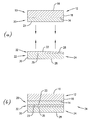
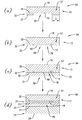
도 1은 예시 5-9에서 추가로 예로 들, 본 발명의 바람직한 실시예를 개략적으로 나타내는 단면도이다.
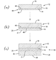
도 2는 두께가 결정되는 방식을 개략적으로 도시한 단면도이다.
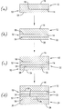
도 3은 예시 10-16에서 추가로 예로 들, 본 발명의 또 다른 실시예를 개략적으로 도시하는 단면도이다.
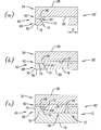
도 4는 예시 17에서 추가로 예로 들, 본 발명의 대안적 실시예를 개략적으로 도시하는 단면도이다.
도 5는 도 4에 도시된 본 발명의 실시예의 변형예를 개략적으로 도시하는 단면도이다.
도 6은 본 발명의 대안적 실시예를 개략적으로 도시하는 단면도이다.
도 7은 도 6에 도시된 실시예의 변형예를 개략적으로 도시하는 단면도이다.
도 8은 본 발명의 대안적 실시예를 개략적으로 도시하는 단면도이다.
도 9는 도 6에 도시된 실시예의 변형예를 개략적으로 도시한 단면도로서, 예시 18에서 예로 든 공정과 유사하다. 1 is a cross-sectional view schematically showing a preferred embodiment of the present invention further as an example in Example 5-9.
2 is a cross-sectional view schematically showing how the thickness is determined.
3 is a cross-sectional view schematically showing yet another embodiment of the present invention, for example, further shown in Examples 10-16.
4 is a cross-sectional view schematically showing an alternative embodiment of the present invention, as further illustrated in Example 17. FIG.
5 is a cross-sectional view schematically showing a modification of the embodiment of the present invention shown in FIG.
6 is a cross-sectional view schematically showing an alternative embodiment of the present invention.
FIG. 7 is a cross-sectional view schematically showing a modification of the embodiment shown in FIG. 6.
8 is a cross-sectional view schematically showing an alternative embodiment of the present invention.
FIG. 9 is a cross-sectional view schematically showing a variation of the embodiment shown in FIG. 6, similar to the process illustrated in Example 18. FIG.
더 구체적으로, 본 발명은 다층 본딩 스킴을 이용해 마이크로전자 구조물을 형성하는 방법을 제공한다. 본 발명의 특정 선호되는 실시예가 도면에 도시되고 명세서에 기재되지만, 이러한 개시는 예에 불과하다. 본 발명의 실시예는 본 발명의 이상적인 실시예를 개략적으로 도시하는 횡단면 도시를 참고하며 본원에 기재된다. 따라서 예를 들어 도시된 형태로부터의 제조 기법 및/또는 허용오차의 변동이 예상될 것이다. 본 발명의 원리를 개시된 특정 실시예로 한정하려 하는 것은 아니다. 예를 들어, 도면에서, 층과 영역의 크기와 상대적 크기가 명료성을 위해 과장될 수 있다. 덧붙여, 본 발명의 실시예는 본원에 설명된 영역의 특정 형태로 제한되는 것으로 이해되어서는 안되며, 예를 들어 제작의 결과로서 상기 형태에서 벗어난 것도 포함하는 것으로 이해되어야 한다. 예를 들어, 사각형으로 도시된 영역은 둥근형이거나 만곡형 특징부를 가질 수 있다. 따라서 도면에 도시된 영역은 개략적인 것이며, 이들의 형태는 소자의 영역 또는 토포그래피의 영역의 정확한 형태를 도시하려는 의도가 아니며 본 발명의 범위를 제한하려는 의도도 아니다.
More specifically, the present invention provides a method of forming a microelectronic structure using a multilayer bonding scheme. While certain preferred embodiments of the invention are shown in the drawings and described in the specification, this disclosure is merely an example. Embodiments of the present invention are described herein with reference to cross-sectional views that schematically illustrate ideal embodiments of the present invention. Thus, for example, variations in manufacturing techniques and / or tolerances from the depicted form would be expected. It is not intended to be exhaustive or to limit the principles of the invention to the specific embodiments disclosed. For example, in the figures, the size and relative size of layers and regions may be exaggerated for clarity. In addition, embodiments of the present invention should not be understood as being limited to the particular forms of the regions described herein, but are to be understood to include deviations from these forms, for example as a result of fabrication. For example, the regions shown as squares may have rounded or curved features. Accordingly, the regions shown in the figures are schematic, and their forms are not intended to depict the exact form of the regions of the device or the regions of the topography, nor are they intended to limit the scope of the invention.
1. 2층 본딩 스킴 Ⅰ (bilayer bonding scheme Ⅰ)1. Bilayer Bonding Scheme Ⅰ
도 1(a)를 참조하면, 전구 구조물(10)이 개략적인 횡단면도로 도시된다. 구조물(10)은 제 1 기판(12)을 포함한다. 기판(12)은 전면, 즉 소자 표면(14)과, 후면(16)과, 최외 변부(outermost edge)(18)를 가진다. 기판(12)은 임의의 형태를 가질 수 있지만, 통상적으로 원의 형태를 가질 것이다. 바람직한 제 1 기판(12)은 소자 웨이퍼, 가령, 집적 회로, MEMS, 마이크로센서, 전력 반도체, 발광 다이오드, 광자 회로, 인터포저, 내장형 수동 소자, 및 실리콘 및 그 밖의 다른 반도체 물질, 가령, 실리콘-게르마늄, 갈륨 비소, 및 갈륨 니트라이드로 제조된 그 밖의 다른 마이크로소자로 구성된 군 중에서 선택된 소자들의 어레이(도면에 도시되지 않음)를 포함하는 소자 표면을 갖는 소자 웨이퍼를 포함한다. 이들 소자의 표면은 이하의 물질 중 하나 이상으로부터 형성된 구조물(도면에 도시되지 않음)을 포함하는 것이 일반적이다: 실리콘, 폴리실리콘, 실리콘 디옥사이드, 실리콘 (옥시)니트라이드, 금속(가령, 구리, 알루미늄, 금, 텅스텐, 탄탈럼), 로우 k 유전체(low k dielectric), 폴리머 유전체, 및 다양한 금속 니트라이드 및 실리사이드. 소자 표면(14)은 또한, 솔더 범프, 금속 포스트(metal post), 금속 필러(metal pillar), 및 실리콘, 폴리실리콘, 실리콘 디옥사이드, 실리콘 (옥시)니트라이드, 금속, 로우 k 유전체, 폴리머 유전체, 금속 니트라이드, 및 금속 실리사이드로 구성된 군 중에서 선택된 물질로부터 형성된 구조물로 구성된 군 중에서 선택된 적어도 하나의 구조물을 포함할 수 있다. Referring to FIG. 1A, the
도 1(a)에 도시된 것처럼, 조성물이 제 1 기판(12)에 도포되어, 소자 표면(14) 상에 제 1 본딩 층(20)을 형성할 수 있다. 본딩 층(20)은 제 1 기판(12)으로부터 멀리 떨어진 상부 표면(21)을 가지며, 바람직하게는 제 1 본딩 층(20)이 소자 표면(14)에 바로 접하게 형성된다(즉, 제 1 본딩 층(20)과 기판(12) 사이에 어떠한 중간 층도 없다). 조성물은 임의의 공지된 도포 방법에 의해 도포될 수 있으며, 한 가지 바람직한 방법은 조성물을 약 5초 내지 약 120초 (바람직하게는 약 30초 내지 약 90초)의 시간 주기 동안 약 500rmp 내지 약 5,000rpm (바람직하게는 약 500rmp 내지 약 2,000rpm)으로 스핀-코팅하는 것이 있다. 조성물이 도포된 후, 약 60초 내지 약 8분 (바람직하게는, 약 90초 내지 약 6분) 동안, 약 80℃ 내지 약 250℃, 더 바람직하게는, 약 170℃ 내지 약 220℃의 온도까지 가열되는 것이 바람직하다. 제 1 본딩 층(20)을 형성하기 위해 사용되는 조성물에 따라, 층(20)을 경화하기 위해 베이킹 공정이 가교 반응을 개시할 수 있다. 일부 실시예에서, 사용되는 조성물에 따라, 층을 다단계 베이킹 공정을 겪도록 하는 것이 바람직하다. 또한 일부 경우, 복수의 단계로 제 1 본딩 층(20)이 제 1 기판(12)상에 "쌓아지도록(build)", 조성물의 추가 분취량에 상기의 도포 및 베이킹 공정이 반복될 수 있다. As shown in FIG. 1A, a composition may be applied to the
제 2 전구 구조물(22)이 또한 도 1(a)의 개략적인 횡단면도에 도시된다. 제 2 전구 구조물(22)이 제 2 기판(24)을 포함한다. 이 실시예에서, 제 2 기판(24)은 캐리어 웨이퍼이다. 즉, 제 2 기판(24)은 전면, 즉 캐리어 표면(26)과, 후면(28)과, 최외 변부(30)를 가진다. 제 2 기판(24)은 임의의 형태를 가질 수 있지만, 원의 형태를 가질 것이며 제 1 기판(12)과 유사한 크기를 가질 것이다. 바람직한 제 2 기판(24)은 실리콘, 사파이어, 석영, 금속(가령, 알루미늄, 구리, 강), 및 다양한 유리 및 세라믹을 포함한다. The
도 1(a)에 도시된 것처럼, 제 2 조성물이 제 2 기판(24)으로 도포되어, 캐리어 표면(26) 상에 제 2 본딩 층(32)을 형성할 수 있다. 제 2 본딩 층(32)은 제 2 기판(24)으로부터 멀리 떨어진 상부 표면(33)과, 제 2 기판(24)에 접하는 하부 표면(35)을 가진다. 바람직하게는, 제 2 본딩 층(32)은 캐리어 표면(26)에 직접 접하게 형성된다(즉, 제 2 본딩 층(32)과 제 2 기판(24) 사이에 어떠한 중간 층도 없음). 조성물은, 임의의 공지된 도포 방법에 의해 도포될 수 있고, 한 가지 바람직한 방법은 약 5초 내지 약 120초(바람직하게는, 약 30초 내지 약 90초)의 시간 주기 동안, 약 500rmp 내지 약 5,000rpm(바람직하게는, 약 500rmp 내지 약 2,000rpm)의 속도로 조성물을 스핀-코팅하는 것이다. 조성물이 도포된 후, 약 80 ℃ 내지 약 250 ℃, 더 바람직하게는, 약 170℃ 내지 약 220 ℃의 온도까지로, 약 60초 내지 약 8분 (바람직하게는, 약 90초 내지 약 6분)의 시간 주기 동안 가열되는 것이 바람직하다. 제 2 본딩 층(32)을 형성하기 위해 사용되는 조성물에 따라서, 층(32)을 경화시키기 위해 베이킹이 가교 반응을 개시할 수 있다. 일부 실시예에서, 사용되는 조성물에 따라, 층을 다단계 베이킹 공정을 겪게 하는 것이 바람직하다. As shown in FIG. 1A, a second composition may be applied to the
제 1 및 제 2 본딩 층(20 및 32)(및 본원에 기재되는 그 밖의 다른 층)의 두께는 도 2를 참조하여 최적으로 도시될 수 있으며, 여기서, 유사한 도면부호가 유사한 부분을 나타내기 위해 사용되었다. 상기에서 기재된 소자 뿐 아니라, 소자 표면(14) 상에 존재하거나 상기 소자 표면(14) 내에 존재하는 상승된 특징부, 접촉 홀(contact hole), 비아 홀(via hole), 라인(line), 트렌치(trench) 등의 존재로 인한 소자 표면(14) 상의 토포그래피의 변동을 개략적으로 도시하기 위해 소자 표면(14)이 도 2에 도시되어 있다. 다양한 특징부들 중에서, 최고 특징부(36)와 최저 특징부(38)가 소자 표면(14)상에서 발견된다. (본원에 기재될 때, "최고(highest)"은 기판(12)의 후면(16)으로부터 가장 멀리 뻗어 있는 특징부를 일컫고, "최저(lowest)"는 제 1 기판(12)의 후면(16)에 가장 가까운 최저점을 갖는 특징부를 일컫는다.) 최고 특징부(36)는 최상부 표면(36a)을 가지며, 최저 특징부(38)는 최하부 표면 또는 점(38a)을 가진다. 토포그래피적(즉, 비-평탄형) 표면에 도포된 층의 두께를 지칭할 때, 두 가지 두께가 참조될 수 있다. T1은 최하부 표면 또는 점(38a)에 의해 형성되는 하부 평면(40)으로부터 상부 표면(21)까지의 거리를 일컬으며, 도 2에 예가 나타나 있다. T2는 최상부 표면(36a) 상부에서 측정된 층의 두께를 지칭한다. 구체적으로, 그리고 도 2에 도시된 것처럼, 이 두께 T2는 상부 평면(42)으로부터 시작하여, 상부 표면(21)까지 뻗어 있다. 평탄한(또는 실질적으로 평탄한) 표면에 도포되는 층의 두께를 지칭할 때, 상기 두께는 도 2에서 T3으로 나타내어지고, 층(32)의 하부 표면(35)과 상부 표면(33) 사이의 거리이다. 마지막으로, 일부 경우, 두께 T4가 사용되고, 이는 하부 평면(40)에서부터 상부 평면(42)까지의 거리를 일컫는다. 모든 두께는 5회 측정에 걸쳐 취해진 평균 두께를 지칭한다. The thickness of the first and second bonding layers 20 and 32 (and other layers described herein) may be optimally shown with reference to FIG. 2, where like reference numerals designate similar parts. Was used. In addition to the devices described above, raised features, contact holes, via holes, lines, trenches present on or within the
본 발명의 실시예에서, 제 1 본딩 층(20)은, T4와 적어도 동일한, 바람직하게는 약 1.1T4 내지 약 1.5T4, 더 바람직하게는 약 1.2T4 내지 약 1.3T4인 두께 T1을 갖는 것이 바람직하다. 일반적으로 이는 적어도 약 24㎛, 더 바람직하게는 약 45㎛ 내지 약 200㎛, 더 더욱 바람직하게는 약 50㎛ 내지 약 150㎛인 두께 T1을 도출할 것이다. 덧붙이자면, 제 1 본딩 층(20)은 적어도 약 5㎛, 더 바람직하게는 약 5㎛ 내지 약 50㎛, 더 더욱 바람직하게는 약 10㎛ 내지 약 30㎛인 두께 T2를 갖는 것이 바람직하다. 제 2 본딩 층(32)은 약 35㎛ 미만, 바람직하게는 약 1㎛ 내지 약 35㎛, 더 바람직하게는 약 1㎛ 내지 약 25㎛, 더 더욱 바람직하게는 약 1㎛ 내지 약 15㎛의 두께 T3를 가진다.In an embodiment of the invention, the
제 1 본딩 층(20)은 제 2 본딩 층(32)의 연화 온도보다 적어도 약 20℃ 더 높은, 더 바람직하게는 약 20℃ 내지 약 200℃ 더 높은, 더 더욱 바람직하게는 약 20℃ 내지 약 100℃ 더 높은 연화점(softening point)(링 앤드 볼(ring and ball))을 갖는 것이 바람직하다. 이는 일반적으로, 적어도 약 100℃, 바람직하게는 약 150℃ 내지 약 400℃, 더 바람직하게는 약 200℃ 내지 약 300℃의 연화점을 갖는 제 1 본딩 층(20)을 도출할 것이다. 추가로, 제 2 본딩 층(32)의 통상적인 연화점은 약 220 ℃ 미만, 바람직하게는 약 50 ℃ 내지 약 220 ℃, 더 바람직하게는 약 100℃ 내지 약 150℃일 것이다. The
제 1 및 제 2 본딩 층(20 및 32)이 형성되는 물질은 각각 제 1 및 제 2 기판(12 및 24)과의 강력한 접착성 본드뿐 아니라 서로 간의 강력한 접착성 본드까지 형성할 수 있어야 한다. ASTM D4541/D7234에 의해 결정된 바와 같이, 약 50 psig 초과, 바람직하게는, 약 80 psig 내지 약 250 psig, 더 바람직하게는, 약 100 psig 내지 약 150 psig의 접착 강도를 갖는 것은 어느 것이나 제 1 및 제 2 본딩 층(20 및 32)으로서 사용되기에 바람직할 것이다. The material on which the first and second bonding layers 20 and 32 are formed should be able to form not only strong adhesive bonds with the first and
바람직하게는, 제 1 및 제 2 본딩 층(20 및 32)에서 사용되기 위한 조성물은, 상기의 속성을 갖는 층이 될 수 있을 상용화된 본딩 조성물로부터 선택될 수 있다. 일반적인 이러한 조성물은 유기물이며, 용매계에서 용해되거나 분산되는 폴리머 또는 올리고머를 포함할 것이다. 폴리머 또는 올리고머는, 고리형 올레핀, 에폭시, 아크릴류(acrylics), 실리콘류(silicones), 스티렌류(styrenics), 비닐 할라이드, 비닐 에스테르, 폴리아미드, 폴리이미드, 폴리술폰, 폴리에테르술폰, 고리형 올레핀, 폴리올레핀 고무, 및 폴리우레탄, 에틸렌-프로필렌 고무, 폴리아미드 에스테르, 폴리이미드 에스테르, 폴리아세탈, 및 폴리비닐 부티랄의 폴리머 및 올리고머로 구성된 군 중에서 선택되는 것이 일반적이다. 통상의 용매계는 폴리머 또는 올리고머 선택에 따라 달라질 것이다. 조성물의 일반적인 고체 함량은, 조성물의 총 중량을 100 중량%이라 하면, 약 1중량% 내지 약 60중량%, 바람직하게는 약 3중량% 내지 약 40중량%일 것이다. 일부 적합한 조성물이 미국 특허 공개 번호 2007/0185310, 2008/0173970, 2009/0038750, 및 2010/01 12305에 기재되어 있으며, 상기 미국 특허는 본원에서 참조로서 포함된다. Preferably, the composition for use in the first and second bonding layers 20 and 32 may be selected from commercially available bonding compositions which may be layers having the above properties. Typical such compositions are organic and will include polymers or oligomers that are dissolved or dispersed in the solvent system. Polymers or oligomers are cyclic olefins, epoxies, acrylics, silicones, styrenics, vinyl halides, vinyl esters, polyamides, polyimides, polysulfones, polyethersulfones, cyclics It is generally selected from the group consisting of polymers and oligomers of olefins, polyolefin rubbers and polyurethanes, ethylene-propylene rubbers, polyamide esters, polyimide esters, polyacetals, and polyvinyl butyral. Conventional solvent systems will depend on the polymer or oligomer selection. The general solids content of the composition will be from about 1% to about 60% by weight, preferably from about 3% to about 40% by weight, based on 100% by weight of the total weight of the composition. Some suitable compositions are described in US Patent Publication Nos. 2007/0185310, 2008/0173970, 2009/0038750, and 2010/01 12305, which are incorporated herein by reference.
그 후, 구조물(10 및 22)은 면대면(face-to-face) 관계로 함께 가압되어, 제 1 본딩 층(20)의 상부 표면(21)이 제 2 본딩 층(32)의 상부 표면(33)과 접촉하게 된다(도 1(b)). 가압 동안, 충분한 압력과 열이 충분한 시간 동안 적용되어, 2개의 구조물(10 및 22)의 본딩이 발생하여, 본딩된 스택(34)이 형성될 수 있다. 본딩 파라미터는 본딩 층(20 및 32)이 형성되는 조성물에 따라 달라질 것이지만, 이 단계 동안의 통상의 온도는 약 150℃ 내지 약 375 ℃, 바람직하게는, 약 160℃ 내지 약 350℃일 것이며, 약 30초 내지 약 5분, 더 바람직하게는, 약 2분 내지 약 4분의 시간 주기 동안의, 약 1,000N 내지 약 5,000N, 바람직하게는 약 2,000N 내지 약 4,000N의 통상의 압력이 있을 것이다. The
이 단계에서, 제 1 기판(12)은 안전하게 핸들링되고, 다른 경우라면 제 2 기판(24)으로 본딩되지 않고 제 1 기판(12)에 손상을 입힐 수 있을 추가 공정의 대상이 될 수 있다. 따라서 구조물은 안전하게, 후면 가공, 가령, 후면-연삭(back-grinding), CMP, 에칭, 금속 및 유전체 증착, 패터닝(가령, 포토리소그래피, 비아 에칭), 부동태화(passivation), 어닐링, 및 이들의 조합을 겪을 수 있으며, 이때, 이들 후속 공정 단계 동안 기판(12 및 24)의 분리가 발생하지 않고, 임의의 화학물의 침투(infiltration)에 직면하지 않는다. 제 1 본딩 층(20) 및 제 2 본딩 층(32)이 이들 공정을 견딜 수 있을 뿐 아니라, 최대 약 450 ℃, 바람직하게는 약 200℃ 내지 약 400℃, 더 바람직하게는, 약 200℃ 내지 약 350℃의 공정 온도를 견딜 수도 있다. In this step, the
공정이 완료되면, 기판(12 및 24)은 임의의 개수의 분리 방법(도시되지 않음)에 의해 분리될 수 있다. 한 가지 방법은 제 1 및 제 2 본딩 층(20, 32) 중 하나 또는 둘 모두를 용매(가령, 리모넨, 도데켄, 프로필렌 글리콜 모노메틸 에테르(PGME))에서 용해시키는 것과 관련된다. 또는, 먼저, 레이저 절삭, 플라스마 에칭, 수류 분사(water jetting), 또는 제 1 및 제 2 본딩 층(20, 32)을 효과적으로 에칭하거나 분해하는 그 밖의 다른 고에너지 기법을 이용해, 제 1 및 제 2 본딩 층(20, 32) 중 하나 또는 둘 모두의 주변부(periphery)를 기계적으로 분열(disrupt)하거나 파괴함으로써, 기판(12 및 24)이 분리될 수 있다. 제 1 및 제 2 본딩 층(20, 32)을 관통해 톱질(saw)하거나 절단하는 것, 또는 이와 동등한 수단에 의해 층(20, 32)을 둘로 쪼개는 것(cleave)도 적합하다. 상기의 수단들 중 어느 것이 사용되는지와 무관하게, 그 후, 기판(12 및 14)을 완전히 분리하기 위해 낮은 기계적 힘(가령, 손가락 압력, 부드럽게 쐐기박기(gentle wedging))이 가해질 수 있다. Once the process is complete, the
가장 선호되는 분리 방법은 본딩된 스택(34)을 적어도 약 100℃, 바람직하게는 약 150℃ 내지 약 220℃, 더 바람직하게는 약 180℃ 내지 약 200℃의 온도까지 가열하는 것을 포함한다. 이들 온도에서, 제 2 본딩 층(32)은 연화될 것이며, 이에 따라서, 기판(12 및 24)이 분리될 수 있음을 알 것이다(가령, 슬라이딩 디본딩 방법에 의해, 가령, 미국 특허 공개 번호 2008/0200011에 기재된 방법에 의해 분리될 수 있으며, 상기 미국 특허는 본원에서 참조로서 포함된다). 분리 후, 특정 층(20 또는 32)을 용해시킬 수 있는 용매에 의해, 임의의 남아 있는 제 1 또는 제 2 본딩 층(20 및 32)이 제거될 수 있다. 일부 실시예에서, 제 1 본딩 층(20)을 형성하기 위한 조성물은, 제 1 기판(12) 상에 상기 조성물의 일부 또는 전부가 영구적으로 남아 있기에 적합하도록 선택될 것이다. 이러한 경우, 제 1 본딩 층(20)은 후속하는 웨이퍼 공정 단계에서 일부 기능(가령, 갭 충전(gap fill))을 수행할 것이며, 이는 종래 기술 공정에는 없는 이점이다. Most preferred separation methods include heating the bonded
이 2층(bilayer) 실시예는 많은 이점을 제공함을 알 것이다. 본 발명에 의해, 본딩 온도 및 구조물의 전체 열 안정성이 제어될 수 있다. 즉, 본 발명에 의해, 본딩 및 디본딩을 더 낮은 온도에서 가능하게 하면서 동시에 더 높은 공정 온도의 사용이 가능해진다.
It will be appreciated that this bilayer embodiment provides many advantages. By the present invention, the bonding temperature and the overall thermal stability of the structure can be controlled. That is, the present invention enables bonding and debonding at lower temperatures and at the same time the use of higher process temperatures.
2. 2층 본딩 스킴 Ⅱ2. Two Layer Bonding Scheme Ⅱ
두 번째 2층 본딩 스킴이 도 3에 도시되어 있으며, 여기서 유사한 도면번호가 유사한 부분을 나타낸다. 이 실시예에서, 상부 표면(46)과 하부 표면(48)을 갖는 "세정(cleaning)" 또는 리프트-오프 층(lift-off layer)(44)이 소자 표면(14) 상에 형성된다. 리프트-오프 층(44)은 임의의 알려진 도포 방법에 의해 형성될 수 있으며, 한 가지 선호되는 방법이, 약 5초 내지 약 120초 (바람직하게는, 약 30초 내지 약 90초)의 시간 주기 동안, 약 500rmp 내지 약 5,000rpm (바람직하게는, 약 500rmp 내지 약 2,000rpm)의 속도로 층(44)을 형성하기 위해 사용되는 조성물을 스핀-코팅하는 것이다. 조성물이 도포된 후, 약 60초 내지 약 4분 (바람직하게는, 약 90초 내지 약 2분)의 시간 주기 동안, 상기 조성물은 약 60 ℃ 내지 약 250 ℃, 더 바람직하게는, 약 80 ℃ 내지 약 220 ℃의 온도까지로 가열되는 것이 바람직하다. 일부 실시예에서, 사용되는 조성물에 따라, 층이 다단계 베이킹 공정을 겪게하는 것이 바람직하다. 리프트-오프 층(44)을 형성하기 위해 사용되는 조성물에 따라, 층(44)을 경화하기 위해 베이킹이 가교 반응을 개시할 수도 있다. A second two layer bonding scheme is shown in FIG. 3, where like reference numerals refer to like parts. In this embodiment, a "cleaning" or lift-
리프트-오프 층(44)은 약 3㎛ 미만, 더 바람직하게는 약 0.5㎛ 내지 약 3㎛, 더 더욱 바람직하게는 약 1㎛ 내지 약 1.5㎛의 두께 T1를 갖는 것이 바람직하다. 또 다른 실시예에서, 리프트-오프 층(44)은 컨포멀 층(conformal layer)이며, 따라서 상기의 두께를 갖지 않을 것이다. The lift-
리프트-오프 층(44)을 형성하기 위해 사용되는 조성물은, 상기 층(44)이, 1 % 염산 수용액, 50% 아세트산 수용액, 이소프로판올, 1-도데켄, R-리모넨, 시클로펜타논, PGME, 및 테트라메틸암모늄 히드록사이드(TMAH)으로 구성된 군 중에서 선택된 용액에 가용성(soluble)이도록 선택되어야 한다. 더 구체적으로, 리프트-오프 층(44)은 특정 제거 용액과 약 4-5시간 접촉한 후, 적어도 약 95%, 바람직하게는 적어도 약 99%, 바람직하게는 100% 용해/제거될 것이다. The composition used to form the lift-
리프트-오프 층(44)을 형성하기 위한 바람직한 조성물은 상기의 속성을 갖는 상용화된 조성물 중에서 선택될 수 있다. 이러한 조성물의 예로는, 폴리(비닐 피리딘) 및 폴리아믹 산으로 구성된 군 중에서 선택된 것들이 있다. 이러한 바람직한 두 가지 조성물로는 습식-현상 가능한(wet-developable) 물질의 ProLIFT® 및 WGF 시리즈(Brewer Science, Inc. 제공)가 있다. 사용되기에 특히 바람직한 조성물이 미국 특허 공개 번호 2009/0035590에 기재되어 있으며, 상기 미국 특허는 본원에서 참조로서 포함된다. Preferred compositions for forming the lift-
그 후 본딩 층(20)이 리프트-오프 층(44) 상에 형성된다(도 3(b)). 본딩 층(20)은 도 1과 관련하여 기재된 두께 T1와, 적어도 약 5㎛, 더 바람직하게는, 약 5㎛ 내지 약 50㎛, 더 더욱 바람직하게는 약 10㎛ 내지 약 30㎛의 두께 T2를 갖는 것이 바람직하다. 그 후, 제 2 기판(24)이 앞서 기재된 것처럼 본딩 층(20)에 본딩되어, 본딩된 스택(50)을 형성할 수 있다. 그 후, 본딩된 스택(50)은 앞서 기재된 것과 같은 추가 공정의 대상이 될 수 있다. A
제 1 및 제 2 기판(12 및 24)이 분리될 준비가 되면, 본딩된 스택(50)은 상기의 제거 용액들 중 하나에 (바람직하게는 약 1분 내지 약 5시간, 더 바람직하게는 약 2분 내지 약 60분의 시간 주기 동안) 노출되어, 용액이 리프트-오프 층(44)을 용해할 것이며, 이로써, 기판(12 및 24)이 분리될 수 있다. 바람직하게는, 리프트-오프 층(44)이 "세정(cleaning)" 층으로서 기능하는 실시예에서, 기판(12 및 24)이 분리될 수 있기에 충분히 본딩 층(20)을 연화하도록 가열함으로써, 기판(12 및 24)은 분리될 수 있다. 기판(12 및 24)이 분리되면, 제거 용액에 의해 리프트-오프/세정 층(44)이 제거될 수 있고, 이는 본딩 층(20)의 임의의 잔여물도 역시 제거될 수 있도록 할 것이다.
Once the first and
3. 3층 본딩 스킴 Ⅰ(Trilayer Bonding Scheme Ⅰ)3. Trilayer Bonding Scheme I
첫 번째 3층 본딩 스킴이 도 4에 도시되며, 유사한 번호가 유사한 부분을 나타낸다. 도 3의 제 1 본딩 층(20)이 제 2 본딩 층(32)으로 변경됐고, "세정" 또는 리프트-오프 층(44)과 제 2 본딩 층(32) 사이에 추가 층이 추가된 것을 제외하고, 도 4에 도시된 실시예는 도 3에 도시된 것과 유사하다. 특히, (이전에 기재된 것처럼, 그리고 도 4(a)를 참조하라) 리프트-오프 층(44)이 소자 표면(14) 상에 형성된 후, 상부 표면(54)과 하부 표면(56)을 갖는 강성 층(rigid layer)(52)이 리프트-오프 층(44)의 상부 표면(46) 상에 형성된다(도 4(b)). 본원에서 사용될 때, "강성"은 유동계(rheometer)에 의해 판단될 때 적어도 1GPa의 높은 전단계수(shear modulus)를 갖는 층을 지칭한다. 덧붙이자면, "강성"은 공정 온도(일반적으로, 약 1500℃ 내지 약 400℃, 바람직하게는 약 200℃ 내지 약 300℃)에서 유동하지 않는 층을 지칭한다. The first three-layer bonding scheme is shown in FIG. 4, where like numbers refer to like parts. The
강성 층(52)을 형성하기 위해 사용되는 조성물은 제 1 본딩 층(20)과 관련해 앞서 언급된 것과 동일한 유형의 조성물일 것이다. 덧붙여, 강성 층(52)은 제 1 본딩 층(20)과 관련하여 앞서 기재된 것과 유사한 방식으로(가령, 리프트-오프 층(44)의 속성이 컨포멀한 경우, 도 1과 관련해 기재된 것과 유사한 두께로) 형성될 것이다. 강성 층(52)은 (리프트-오프 층(44)의 속성이 컨포멀하지 않은 경우) 약 1㎛ 내지 약 35㎛, 더 바람직하게는, 약 1㎛ 내지 약 25㎛, 더 더욱 바람직하게는, 약 1㎛ 내지 약 15㎛의 두께 T3를 갖는 것이 바람직하다.The composition used to form the
도 4(c)를 참조하면, 앞서 기재된 것과 동일한 도포 방법과 조성물의 유형을 이용해 제 2 본딩 층(32)이 강성 층(52)의 상부 표면(54) 상에 형성된다. 이 실시예에서, 제 2 본딩 층(32)의 두께 T3는 약 1㎛ 내지 약 35㎛, 더 바람직하게는, 약 1㎛ 내지 약 25㎛, 더 더욱 바람직하게는, 약 1㎛ 내지 약 15㎛이다. Referring to FIG. 4 (c), a
바람직하게는 강성 층(52)은 제 2 본딩 층(32)의 연화점보다 적어도 약 20℃ 더 높은, 더 바람직하게는 약 20℃ 내지 약 300℃ 더 높은, 더 더욱 바람직하게는 약 20 ℃ 내지 약 100℃ 더 높은 연화점을 가진다. 이는 일반적으로, 적어도 약 100℃, 바람직하게는 약 150℃ 내지 약 400℃, 더 바람직하게는 약 200℃ 내지 약 300℃의 연화점을 갖는 강성 층(52)을 도출할 것이다. Preferably the
앞서 기재된 바와 같이 제 2 기판(24)은 본딩 층(32)에 본딩되어, 본딩된 스택(58)을 형성할 수 있다(도 4(d)). 그 후, 본딩된 스택(58)은 앞서 기재된 바와 같이 추가 공정의 대상이 될 수 있다. 제 1 및 제 2 기판(12 및 24)이 분리될 준비가 되면, 본딩된 스택(58)은 앞서 기재된 제거 용액들 중 하나에 노출되어, 용액이 리프트-오프 층(44)을 용해하게 되어 따라서 기판(12 및 24)이 분리될 수 있다. 또는 앞서 기재된 바와 같이, 본딩 층(32)을 연화하도록 스택(58)을 가열함으로써, 분리가 개시될 수 있다. 이러한 후자의 경우, 리프트-오프 층(44)은 세정 층으로서 다시 기능하며, 제거 용액에 의해 층(44)을 제거함으로써 본딩 층 잔여물이 제거될 수 있다.
As described above, the
4. 3층 본딩 스킴 Ⅱ4. Three Layer Bonding Scheme Ⅱ
또 다른 3층 본딩 스킴이 도 5(a)-5(d)에서 나타나며, 여기서 유사한 번호는 유사한 부분을 나타낸다. 이 실시예는 상기의 실시예의 변형으로서, 여기서 다층 본딩 시스템이 2개의 강성 층(52)을 포함하며, 이때 제 2 본딩 층(32)이 2개의 층(52) 사이에 위치한다. 조성물 선택, 공정 파라미터 및 단계들 등은 대응하는 층에 대해 앞서 기재된 것과 동일하다. 나타나지 않더라도, 이 실시예는 강성 층(52) 중 하나와 본딩 층(32)을 반전시킴으로써, 수정될 수 있다.
Another three-layer bonding scheme is shown in Figures 5 (a) -5 (d), where like numerals indicate similar parts. This embodiment is a variation of the above embodiment wherein the multilayer bonding system comprises two
5. 기판 변부에 위치하는 복수 층5. Multiple layers located on the edge of the substrate
본 발명의 추가 실시예가 도 6 및 7에 도시되며, 유사한 부분들은 유사한 방식으로 번호 매겨진다. 이들 실시예의 경우, 미국 특허 공개 번호 2009/0218560를 참조하며, 상기 미국 특허는 본원에서 참조로서 포함된다. Further embodiments of the invention are shown in FIGS. 6 and 7, wherein like parts are numbered in a similar manner. For these examples, see US Patent Publication No. 2009/0218560, which is incorporated herein by reference.
도 6(a)를 참조하면, 이 실시예에서, 구조물(55)이 도시된다. 제 1 기판(12)의 소자 표면(14)은 주변 영역(57), 중심 영역(59), 및 상기 주변 영역(57)에 위치하는 2층 본딩 시스템(bilayer bonding system)(60)을 포함한다. 시스템(60)은, 상부 표면(64) 및 하부 표면(66)을 갖는 박형 층(박형 층)(62)과, 외부 표면(70), 내부 표면(72), 하부 표면(74) 및 본딩 표면(76)을 포함하는 본딩 세그먼트(68)를 포함한다. 박형 층(62)의 하부 표면(66)은 주변 영역(57)에서 제 1 기판(12)의 소자 표면(14)에 접하며, 본딩 세그먼트(68)의 하부 표면은 박형 층(62)에 접한다. 박형 층(62)은 리프트-오프 층(44)과 관련해 앞서 기재된 것과 유사한 리프트-오프 층이거나, 박형 층(62)은 접착 촉진 층(adhesion promoter layer)일 수 있다. 박형 층이 접착 촉진 층인 경우, 임의의 상용화된 접착 촉진 조성물이 이러한 목적으로 사용될 수 있다. 이러한 조성물의 이러한 예로는 유기 실란(가령, Brewer Science, Inc.가 제공하는 ProTEK® 프라이머(primer))이 있다.Referring to FIG. 6 (a), in this embodiment, the
박형 층(62)은 종래의 방법, 가령, 스핀-코팅하고, 그 후 특정 조성물에 대한 적합한 온도로 베이킹함으로써, 형성될 수 있다. 예를 들어, 앞서 기재된 바와 같이 리프트-오프 층(44)을 형성하기 위해 후속하는 방법이 사용되어 박형 층(62)을 형성할 수 있다. 덧붙여, 도 6(a)가 이러한 층을 주변 영역(58)에만 존재하는 것으로 도시하더라도, 중심 영역(59)에도 존재하도록 박형 층(62)은 소자 표면(14) 전체에 걸쳐 확장될 수 있다. 박형 층(62)은 주변 영역(57)에서, 약 1㎛ 내지 약 35㎛, 더 바람직하게는 약 1㎛ 내지 약 25㎛, 더 더욱 바람직하게는 약 1㎛ 내지 약 15㎛의 두께 T3를 갖는 것이 바람직하다. 박형 층(62)이 전체 소자 표면(14)에 걸쳐 뻗어 있는 경우, 박형 층(62)은 약 0.1㎛ 내지 약 20㎛, 바람직하게는, 약 0.25㎛ 내지 약 10㎛, 더 바람직하게는, 약 1㎛ 내지 약 3㎛의 두께 T1을 가질 것이다. 또 다른 예를 들면, 박형 층(62)은 컨포멀 층일 수 있고, 따라서 상기의 두께를 갖지 않을 것이다. The
본딩 세그먼트(68)가 임의의 상용화된 본딩 조성물, 가령, 제 1 및 제 2 본딩 층(20 및 32)과 관련해 앞서 기재된 것으로부터 형성될 수 있다. 본딩 세그먼트(68)는 일반적으로, 약 2mm 내지 약 15mm, 바람직하게는, 약 2mm 내지 약 10mm, 더 바람직하게는, 약 2mm 내지 약 5mm의 폭 "D"을 가질 것이다. 덧붙이자면, 본딩 세그먼트(68)는 바람직하게는 약 5㎛ 내지 약 100㎛, 더 바람직하게는 약 5㎛ 내지 약 50㎛, 더 더욱 바람직하게는, 약 10㎛ 내지 약 30㎛의 두께 T3을 가진다.
이때, 앞서 언급된 실시예와 관련해 기재된 것처럼 구조물(55)이 제 2 기판(24)에 본딩될 수 있거나, 도 6(b)에 도시된 것처럼, 충전 층(충전 층)(78)이 소자 표면(14)의 중심 영역에 형성될 수 있다. 충전 층(78)은, 본딩 세그먼트(68)와 관련해 앞서 기재된 것와 동일한 두께를 가질 것이다. 일반적으로 충전 층(78)은 용매계에 분산되거나 용해된 모노머, 올리고머, 및/또는 폴리머를 포함하는 물질로 형성된다. 충전 층(78)이 스핀-코팅에 의해 도포될 경우, 이 물질의 고체 함량은 바람직하게는 약 1중량% 내지 약 50중량%, 더 바람직하게는, 약 5중량% 내지 약 40중량%, 더 더욱 바람직하게는 약 10중량% 내지 약 30중량%이다. 적합한 모노머, 올리고머, 및/또는 폴리머의 예로는, 고리형 올레핀 폴리머 및 코폴리머 및 고 원자 불소 함량(약 30중량% 초과)을 갖는 비정질 플루오로폴리머, 가령, 불화 실록산 폴리머, 불화 에틸렌-프로필렌 코폴리머, 펜던트 퍼플루오로알콕시 기를 갖는 폴리머, 및 테트라플루오로에틸렌과 2,2-비스-트리플루오로메틸-4,5-디플루오로-1,3-디옥솔의 코폴리머(특히 선호됨)로 구성된 군 중에서 선택된 것이 있다. 이들 물질의 본딩 강도는 물질의 특정 화학적 구조와 상기 물질을 도포하는 데 사용되는 코팅 및 베이킹 조건에 따라 달라질 것이다. At this time, the
이 실시예에서, 충전 층(78)은 강력한 접착성 본드를 형성하지 않음으로써, 추후의 분리를 용이하게 하는 것이 바람직하다. 일반적으로, 비정질 폴리머 물질은, (1) 저 표면 자유 에너지(low surface free energy)를 갖고, (2) 무점착성(tack-free)이며 유리, 실리콘 및 금속 표면에 강하게 본딩하지 않는 것으로 알려져 있으며(즉, 일반적으로 히드록실 또는 카르복실산 기의 매우 낮은 농도를 가질 것, 바람직하게는 이러한 기를 갖지 않을 것), (3) 용액으로부터 캐스팅(cast)되거나 라미네이팅되기 위해 박형 필름으로 형성될 수 있으며, (4) 일반적인 본딩 조건 하에서, 기판들 사이에 보이드(void) 없는 본드 라인을 형성하면서, 소자 웨이퍼 표면 토포그래피를 충전(fill)하기 위해 유동할 것이고, (5) 고온 또는 고진공 상태에서 수행되는 것이 바람직할 때조차, 후면 가공 동안 발생되는 기계적 응력 하에서, 균열, 유동, 또는 재분배(redistribute)하지 않을 것이다. 본원에서 사용될 때, 저 표면 자유 에너지는 적어도 약 90°의 물과의 접촉각을 보이고, 접촉각 측정치에 의해 판단될 때 약 40 dynes/cm 미만, 바람직하게는 약 30 dynes/cm 미만, 더 바람직하게는 12 dynes/cm 내지 약 25 dynes/cm의 임계 표면 장력 을 보이는 폴리머 물질로서 정의된다. In this embodiment, the
낮은 본딩 강도는 기판에 붙어 있지 않거나 단지 약한 손 압력(가령, 접착성 노트 종이를 디본딩하기 위해 사용될 수 있는 것과 같은 손 압력)만으로 기판으로부터 박리될 수 있는 폴리머 물질을 일컫는다. 따라서 약 50psig 미만, 바람직하게는 약 35psig 미만, 더 바람직하게는 약 1psig 내지 약 30psig의 접착 강도를 갖는 임의의 것이 충전 층(22)으로서 사용되기에 바람직할 것이다. 상기의 속성을 보이는 적합한 폴리머 물질의 예로는, Mitsui사의 APEL®, Ticona사의 TOP AS®, 및 Zeon brands의 ZEONOR®로서 판매되는 일부 고리형 올레핀 폴리머 및 코폴리머, 및 용매-가용성 플루오로폴리머, 가령, Asahi Glass사가 판매하는 CYTOP® 폴리머, 및 DuPont사가 판매하는 TEFLON® AF 폴리머가 있다. 이들 물질의 본딩 강도는 상기 물질을 도포하기 위해 사용되는 코팅 및 베이킹 조건에 따라 달라질 것이다. Low bonding strength refers to a polymeric material that is not attached to the substrate or that can be peeled off from the substrate with only weak hand pressure (eg, hand pressure such as can be used to debond adhesive note paper). Therefore, anything having an adhesive strength of less than about 50 psig, preferably less than about 35 psig, more preferably about 1 psig to about 30 psig, will be preferred for use as the
이때, 도 6(c)에 도시된 본딩된 스택(82)을 형성하기 위해 이전 실시예에서 기재된 단계를 이용해 제 2 기판이 구조물(55)에 본딩될 수 있다. 스택(82)에 대한 바람직한 공정이 완료된 후, 제 1 기판(12)과 제 2 기판(24)이 쉽게 분리될 수 있다. 한 가지 분리 방법에서, 우선, 용매 또는 그 밖의 다른 화학제를 이용해 본딩 세그먼트(68)가 용해된다. 이는 용매에 침지(immersion)하거나, 용매의 제트(jet)를 본딩 세그먼트(68) 상으로 분사하여, 본딩 세그먼트를 용해시킴으로써, 이뤄질 수 있다. 용매 용해가 본딩 세그먼트(68)를 분열(disrupt)시키기 위해 사용될 경우 열가소성 물질의 사용이 특히 바람직하다. 이러한 제거 공정 동안 일반적으로 사용될 수 있는 용매로는, 에틸 락테이트, 시클로헥사논, -메틸 피롤리돈, 지방족 용매(가령, 헥산, 데칸, 도데칸, 및 도데켄), 및 이들의 혼합물로 구성된 군 중에서 선택된 것을 포함한다. At this time, the second substrate may be bonded to the
또한, 먼저, 레이저 절삭, 플라스마 에칭, 수류 분사, 또는 본딩 세그먼트(68)를 효과적으로 에칭하거나 분해하는 그 밖의 다른 고 에너지 기법을 이용해 본딩 세그먼트(68)의 연결성(continuity)을 기계적으로 분열하거나 파괴함으로써, 기판(12 및 24)은 분리될 수 있다. 먼저, 본딩 세그먼트(68)를 관통해 톱질(saw)하거나 절단하거나, 이와 동등한 임의의 수단에 의해 본딩 세그먼트(68)를 둘로 나누는 것이 적합하다. In addition, first by mechanically breaking or breaking the continuity of the
상기 수단들 중 어느 것이 사용되는지에 무관하게, 이 후에, 낮은 기계적 힘(가령, 손가락 압력, 부드럽게 쐐기박기)이 적용되어, 기판(12 및 24)을 완전히 분리할 수 있다. 바람직하게도, 분리는 충전 층(78)과 기판(12 또는 24) 사이의 강력한 접착성 본드를 극복해야 할 필요가 없다. 대신, 분리가 발생하기 위해서는, 주변 영역(57) 내 본딩 세그먼트(68)에서의 접착성 본드를 해제(release)할 필요만 있다. 그 후, 기판(12 및/또는 24)의 표면이 필요에 따라 적절한 용매에 의해 세정 헹굼되어, 임의의 잔여 물질을 제거할 수 있다 Regardless of which of the above means is used, a low mechanical force (eg finger pressure, smooth wedging) can then be applied to completely separate the
상기의 실시예와 관련해, 충전 층(78)의 형성 전에 본딩 세그먼트(68)가 형성되는 것은 한 가지 가능한 형성 순서에 불과함을 알아야 한다. 충전 층(78)을 먼저 형성하고, 그 후 본딩 시스템(60) 또는 본딩 세그먼트(68)를 형성하는 것이 또한 가능하다. 형성 순서는 본 발명에 있어서 핵심적인 것이 아니며, 해당업계 종사자에 의해 변경될 수 있다. In connection with the above embodiment, it should be understood that the
도 7을 참조하면, 본 발명의 또 다른 실시예가 도시되며, 여기서 유사한 번호는 유사한 부분을 나타낸다. 제 1 및 제 2 기판(12 및 24)이 서로 바뀐 것만 제외하고, 이 실시예는 도 6과 유사하다. 즉, 박형 층(62)이 제 1 기판(12)의 소자 표면(14)이 아니라 제 2 기판(24)의 캐리어 표면(26)과 접촉하고, 본딩 세그먼트(68)의 본딩 표면(76)이 제 1 기판(12)의 소자 표면(14)에 본딩된다. 따라서 특정 적용예의 필요 요건에 따라, 박형 층(62)은 본딩 세그먼트(68)의 하부 표면(74) 또는 본딩 표면(76) 또는 둘 모두와 접할 수 있다. 이 실시예에서, 박형 층(62)은 도 6과 관련해 기재된 두께 T3를 가질 것이며, 이들 두께는 전체 박형 층(62)에 걸쳐 유효할 것이다.
Referring to Fig. 7, another embodiment of the present invention is shown wherein like numerals indicate like parts. This embodiment is similar to FIG. 6 except that the first and
6. 기판 변부에 위치하는 존 영역을 갖는 다중 층 6. Multi-Layer with Zone Area Located at the Edge of Substrate
도 8은 본 발명의 추가 실시예를 도시하며, 여기서 유사한 번호는 유사한 부분을 나타낸다. 도 8(a)를 참조하면, 제 2 본딩 층(32)이 제 1 기판(12)의 주변 영역(57)에서만 형성된다. 도포 방법, 바람직한 속성(가령, 연화점), 및 제 2 본딩 층(32)으로서 사용되기 위한 가능한 조성물은 앞서 기재된 것과 같다. 도 8(b)를 참조하면, 상기에서 도 6 및 7과 관련된 기재된 것처럼, 충전 층(78)이 소자 표면(14)의 중심 영역(59)에서 형성된다. 8 shows a further embodiment of the invention, wherein like numerals refer to like parts. Referring to FIG. 8A, the
그 후, 도 8(c)에서 나타나는 것처럼, 제 1 본딩 층(20)은 제 2 본딩 층(32)의 상부 표면(33) 상에 형성되고, 충전 층(78)의 상부 표면(80) 상에 형성되어, 구조물(84)을 형성할 수 있다. 다시 말하자면, 도포 방법, 바람직한 속성, 및 제 1 본딩 층(20)으로서 사용되기 위한 가능한 조성물은 앞서 기재된 것과 같다. 앞서 언급된 실시예와 관련해 기재된 단계들을 이용해 제 2 기판(24)은 구조물(84)에 본딩되어, 도 8(d)에 도시된 것과 같은 본딩된 스택(86)을 형성할 수 있다. (또는, 예시 18에 기재된 것처럼, 도 1에 도시된 단계들의 순서와 유사하게, 제 1 본딩 층(20)이 제 2 기판(24)의 캐리어 표면(21) 상에 대신 형성되고, 그 후, 2개의 구조물이 서로 가압되어, 본딩된 스택(86)을 형성할 수 있다.)Thereafter, as shown in FIG. 8C, the
그 후, 본딩된 스택(86)은 상기에 기재된 추가 프로세싱의 대상이될 수 있다. 제 1 및 제 2 기판(12 및 24)이 분리될 준비가 되면, 본딩된 스택(86)은 제거 용액(가령, 리모넨, 도데켄, PGME)에 노출되어, 용액이 제 2 본딩 층(32)을 용해시켜, 기판(12 및 24)이 분리되게 할 수 있다. The bonded
또는, 앞서 기재된 것처럼 기판(12 및 24)이 분리될 수 있도록, 제 1 본딩 층(20)보다 낮은 연화점을 갖는 제 2 본딩 층(32)을 연화하기 위해 스택(86)을 가열시킴으로써, 분리가 개시될 수 있다. Alternatively, by heating the
도 9를 참조하면, 본 발명의 추가 실시예가 도시되며, 여기서 유사한 번호가 유사한 부분을 나타낸다. 제 1 및 제 2 기판(12 및 24)이 서로 바뀌는 것을 제외하고 이 실시예는 도 8의 실시예와 유사하다. 즉, 제 2 본딩 층(32)과 충전 층(78)은 제 1 기판(12)의 소자 표면(14)이 아니라 제 2 기판(24)의 캐리어 표면(26)과 접촉하고, 제 1 본딩 층(20)은 제 1 기판(12)의 소자 표면(14)에 본딩된다. 따라서, 특정 적용예의 필요 요건에 따라, 제 2 본딩 층(32) 및 충전 층(78)의 위치가 조절될 수 있다. Referring to Fig. 9, a further embodiment of the present invention is shown wherein like numerals indicate like parts. This embodiment is similar to the embodiment of FIG. 8 except that the first and
특정 기판 표면을 실질적으로, 그리고 완전히 덮기 위해 다양한 본딩, 리프트-오프, 및 강성 층이 제시되는 상기의 본딩 스킴 각각에 대하여, 이들 층 중 하나 이상이 (도시되지 않더라도) 특정 기판의 부분에만 뻗어 있도록 수정될 수 있음을 알 것이다. 즉, 특정 기판 표면의 일부분만 상기 특정 층과 접촉할 것이며, 이는 여전히 본 발명의 범위 내에 있을 것이다. For each of the above bonding schemes in which various bonding, lift-off, and rigid layers are presented to substantially and completely cover a particular substrate surface, one or more of these layers may extend only to portions of the particular substrate (not shown). It will be appreciated that it may be modified. That is, only a portion of a particular substrate surface will be in contact with the particular layer, which will still be within the scope of the present invention.
덧붙여, 제 1 기판(소자) 상에 수직 방식으로(one on top of another) 층들이 형성되고, 그 후 제 2 기판(캐리어)과 본딩되도록 나타난 경우라도, 이를 대신하여 모든 층이 제 2 기판 상에 수직 방식으로 형성되고, 그 후 제 1 기판과 본딩될 수 있다. 또는, 하나 이상의 층이 제 1 기판 상에 형성되고, 나머지 층들이 제 2 기판 상에 형성된 후, 두 기판이 서로 본딩될 수 있다. 최종 구조물이 본원에서도시 및/또는 기재된 층 시스템을 갖는 한 순서는 중요하지 않다.
In addition, even if layers are formed on the first substrate (device) one on top of another, and then appear to be bonded with the second substrate (carrier), instead all layers are on the second substrate. It can be formed in a manner perpendicular to and then bonded with the first substrate. Alternatively, after one or more layers are formed on the first substrate and the remaining layers are formed on the second substrate, the two substrates may be bonded to each other. The order is not critical as long as the final structure has the layer system shown and / or described herein.
예시들 Examples
이하의 예시들은 본 발명에 따라 바람직한 방법을 제공한다. 그러나 이들 예시는 설명을 위해 제공되며 상기 예시들의 어느 것도 본 발명의 전체 범위를 제한하는 것은 아님이 이해되어야 한다. The following examples provide a preferred method in accordance with the present invention. However, these examples are provided for illustrative purposes and it should be understood that none of the above examples limit the full scope of the invention.
예시 1 내지 9는 본 발명의 개선된 본딩 성능을 설명한다. 예시 10 내지 16은 디본딩 후 본딩 조성물의 개선된 세정력을 설명한다.
Examples 1-9 illustrate the improved bonding performance of the present invention. Examples 10-16 illustrate the improved cleaning power of the bonding composition after debonding.
예시 1 Example 1
고리형 올레핀 코폴리머(COC) 본딩 조성물 A의 조성Composition of Cyclic Olefin Copolymer (COC) Bonding Composition A
이 배합물에서, 250 그램(gram)의 에텐-노보넨 코폴리머(뉴욕, 라이 브룩에 소재하는 Mitsui Chemicals America, Inc.사가 제공하는 ALP 8008T) 및 3.125그램의 페놀계 항산화제(독일에 소재하는 BASF 사가 제공하는 IRGANOX 1010)가 373.45그램의 R-리모넨(플로리다, 윈터 하벤에 소재하는 Florida Chemical Co.사 제공)과 373.45그램의 시클로옥탄(미주리, 세인트 루이스에 소재하는 Sigma-Aldrich, Inc.사 제공) 내에서 용해되었다. 상기 혼합물은 이의 모든 성분이 용해될 때까지 실온에서 교반되었다. 최종 용액은 25.31%의 고체를 가졌다. In this formulation, 250 grams of ethene-norbornene copolymer (ALP 8008T from Mitsui Chemicals America, Inc., Livebrook, NY) and 3.125 grams of phenolic antioxidants (BASF, Germany) IRGANOX 1010 from the company offers 373.45 grams of R-limonene (provided by Florida Chemical Co. of Winter Haven, FL) and 373.45 grams of cyclooctane (Sigma-Aldrich, Inc. of St. Louis, Missouri) Dissolved in). The mixture was stirred at room temperature until all of its components dissolved. The final solution had 25.31% solids.
예시 2 Example 2
COC 본딩 조성물 B의 조성Composition of COC Bonding Composition B
210.31그램의 에탄-노보넨 코폴리머(켄터키, 플로렌스에 소재하는 Topas Advanced 폴리mers사가 제공하는 Topas 8007)와 62.4그램의 저-분자-중량 COC 폴리머(켄터키, 플로렌스의 Topas Advanced Polymers사가 제공하는 Topas TM)이, 2,800 달톤(Dalton)의 분자 중량을 갖는 4.0그램의 페놀계 항산화제 (Irganox 1010) 및 14.5그램의 폴리이소부틸렌(뉴욕, 온타리오에 소재하는 Scientific Polymer Products, Inc.사 제공)과 함께 706그램의 R-리모넨에서 용해되었다. 상기 혼합물은 모든 재료가 용액 내이도록 실온에서 교반되었다. 용액은 29%의 고체를 가졌다. 210.31 grams of ethane-norbornene copolymer (Topas 8007 from Topas Advanced Polymers, Florence, KY) and 62.4 grams of low-molecular-weight COC polymer (Topas TM from Topas Advanced Polymers, Florence, KY) ) With 4.0 grams of phenolic antioxidant (Irganox 1010) and 14.5 grams of polyisobutylene (provided by Scientific Polymer Products, Inc., Ontario, NY) having a molecular weight of 2,800 Daltons Dissolved in 706 grams of R-limonene. The mixture was stirred at room temperature so that all materials were in solution. The solution had 29% solids.
예시 3 Example 3
COC 본딩 조성물 C의 조성Composition of COC Bonding Composition C
이 배합물에서, 예시 2의 50그램의 COC 본딩 조성물 B가 50그램의 R-리모넨과 혼합되었다. 혼합물은 실온에서 교반되어 용액을 형성했다. 용액은 14.5% 고체를 가졌다. In this formulation, 50 grams of COC bonding composition B of Example 2 was mixed with 50 grams of R-limonene. The mixture was stirred at room temperature to form a solution. The solution had 14.5% solids.
예시 4 Example 4
본딩 조성물 D의 조성Composition of Bonding Composition D
이 배합물에서, 120그램의 웨이퍼BOND® HT-10.10 물질(Brewer Science, inc.사 제공)이 80그램의 1-도데켄(미주리, 세인트 루이스에 소재하는 Sigma-Aldrich)과 혼합되었다. 상기 혼합물은 실온에서 교반되어 용액을 형성했다. In this formulation, 120 grams of wafer BOND® HT-10.10 material (Brewer Science, Inc.) was mixed with 80 grams of 1-dodeken (Sigma-Aldrich, St. Louis, MO). The mixture was stirred at room temperature to form a solution.
예시 5 Example 5
소자 웨이퍼 상의 후막 COC 본딩 조성물 A 층과 캐리어 웨이퍼 상의 박막 COC 본딩 조성물 C 층Thick Film COC Bonding Composition A Layer on Device Wafer and Thin Film COC Bonding Composition C Layer on Carrier Wafer
이 절차에서, 코팅된 기판과 제 2 기판 사이의 효과적인 본딩을 얻기 위해, 270℃에서 충분히 유동하도록 설계된 고리형 올레핀 폴리머 코팅 층인 예시 1의 10mL의 COC 본딩 조성물 A가 200-mm 실리콘 웨이퍼 상에 스핀-코팅되고 베이킹되어(이하에서 기재될 스핀 및 베이킹 파라미터를 이용), COC 본딩 조성물 A의 필름을 형성하였다. 이 공정은 예시 1의 10mL의 COC 본딩 조성물 A의 제 2 분취량에 대해서도 정확히 반복되었으며, 이 제 2 분취량은 제 1 필름의 상부 상에 필름을 형성하기 위해 사용되었다. 두 도포 단계 모두 이후의 최종 필름 두께는 96㎛이었다. In this procedure, 10 mL of COC bonding composition A of Example 1, which is a cyclic olefin polymer coating layer designed to flow sufficiently at 270 ° C., to obtain effective bonding between the coated substrate and the second substrate, is spin on a 200-mm silicon wafer. -Coated and baked (using spin and baking parameters to be described below) to form a film of COC bonding composition A. This process was exactly repeated for the second aliquot of the 10 mL COC bonding composition A of Example 1, which was used to form a film on top of the first film. The final film thickness after both application steps was 96 μm.
코팅된 기판과 제 2 기판 사이에 효과적인 본딩을 얻기 위해 220℃에서 충분히 유동하도록 설계된 고리형 올레핀 폴리머 코팅 층인 예시 3의 COC 본딩 조성물 C가 또 다른 200-mm 실리콘 웨이퍼 상으로 스핀-코팅되었다. COC 본딩 조성물 C의 두께는 약 3㎛이었다. 스핀-코팅 및 베이킹 파라미터는 COC 본딩 조성물 A와 COC 본딩 조성물 C의 경우 서로 동일했으며, 다음과 같다:The COC bonding composition C of Example 3, a cyclic olefin polymer coating layer designed to flow sufficiently at 220 ° C. to obtain effective bonding between the coated substrate and the second substrate, was spin-coated onto another 200-mm silicon wafer. The thickness of the COC bonding composition C was about 3 μm. Spin-coating and baking parameters were the same for COC bonding composition A and COC bonding composition C, as follows:
·스핀-코팅 조건: 60초 동안 10,000rpm/sec의 가속도로 800rpm의 스핀-코팅Spin-coating condition: 800-rpm spin-coating at an acceleration of 10,000 rpm / sec for 60 seconds
·베이킹 조건, 순서대로: 2분 동안 80℃, 2분 동안 110℃, 2분 동안 160℃, 및 6분 동안 220℃.Baking conditions, in order: 80 ° C. for 2 minutes, 110 ° C. for 2 minutes, 160 ° C. for 2 minutes, and 220 ° C. for 6 minutes.
본딩 압력 5,800N을 갖는 압력 챔버 내 가열 진공(heated vacuum)에서, 3분 동안 220℃의 진공 상태에서 앞서 기재된 바와 같이 COC 본딩 조성물 A와 COC 본딩 조성물 C로 코팅된 두 개의 실리콘 웨이퍼는 서로 면대면(face-to-face relationship)으로 본딩되었다. 미국 특허 공개 번호 2010/0206479(미주리, 롤라에 소재하는 Brewer Science, Inc.에 의해 획득된 특허로서 본원에서 참조로서 포함됨)에 기재된 것과 유사한 슬라이딩(sliding) 공정을 이용하는 디본더(debonder)가 220℃에서 상기 본딩된 웨이퍼를 분리했다. In a heated vacuum in a pressure chamber with a bonding pressure of 5800 N, two silicon wafers coated with COC bonding composition A and COC bonding composition C were face-to-face with each other as described above in a vacuum of 220 ° C. for 3 minutes. bonded in a face-to-face relationship. A debonder using a sliding process similar to that described in US Patent Publication No. 2010/0206479 (patent obtained by Brewer Science, Inc., Rolla, Missouri, incorporated herein by reference) is 220 ° C. The bonded wafer was separated at.
예시 6 Example 6
후막 COC 본딩 조성물 A와 박막 COC 본딩 조성물 CThick Film COC Bonding Composition A and Thin Film COC Bonding Composition C
이 절차에서, 코팅된 기판과 제 2 기판 사이의 효과적인 본딩을 얻기 위해 270℃에서 충분히 유동하도록 설계된 고리형 올레핀 폴리머 코팅 층인 예시 1의 10mL의 COC 본딩 조성물 A가 200-mm 실리콘 웨이퍼 상에 스핀-코팅되고 베이킹되어(앞서 기재된 스핀 및 베이킹 파라미터를 이용), COC 본딩 조성물 A의 필름을 형성하였다. 이 공정은 예시 1의 10mL의 COC 본딩 조성물 A의 제 2 분취량에 대해서도 정확히 반복되었으며, 이 제 2 분취량은 제 1 필름의 상부 상에 필름을 형성하기 위해 사용되었다. 두 도포 단계 모두 이후의 최종 필름 두께는 93㎛이었다. In this procedure, 10 mL of COC bonding composition A of Example 1, which is a cyclic olefin polymer coating layer designed to flow sufficiently at 270 ° C. to obtain effective bonding between the coated substrate and the second substrate, was spun on a 200-mm silicon wafer. Coated and baked (using the spin and baking parameters described above) to form a film of COC bonding composition A. This process was exactly repeated for the second aliquot of the 10 mL COC bonding composition A of Example 1, which was used to form a film on top of the first film. The final film thickness after both application steps was 93 μm.
코팅된 기판과 제 2 기판 사이에 효과적인 본딩을 얻기 위해 220℃에서 충분히 유동하도록 설계된 고리형 올레핀 폴리머 코팅 층인 예시 3의 COC 본딩 조성물 C가 COC 본딩 조성물 A 필름의 상부 상으로 스핀-코팅되었다. COC 본딩 조성물 C의 두께는 약 8㎛이었다. 스핀-코팅 및 베이킹 파라미터는 COC 본딩 조성물 A와 COC 본딩 조성물 C의 경우 서로 동일했으며, 다음과 같다:The COC bonding composition C of Example 3, a cyclic olefin polymer coating layer designed to flow sufficiently at 220 ° C. to obtain effective bonding between the coated substrate and the second substrate, was spin-coated onto the top of the COC bonding composition A film. The thickness of the COC bonding composition C was about 8 μm. Spin-coating and baking parameters were the same for COC bonding composition A and COC bonding composition C, as follows:
·스핀-코팅 조건: 60초 동안 10,000rpm/sec의 가속도로 800rpm의 스핀-코팅,Spin-coating condition: 800-rpm spin-coating at an acceleration of 10,000 rpm / sec for 60 seconds,
·베이킹 조건, 순서대로: 4분 동안 110℃, 2분 동안 160℃, 6분 동안 220℃. Baking conditions, in that order: 110 ° C. for 4 minutes, 160 ° C. for 2 minutes, 220 ° C. for 6 minutes.
또 다른 200-mm 실리콘 웨이퍼의 중심이 불화 실란(헵타데카플루오로-1,1,2,2-테트라히드로데실 트리클로로실란)으로 코팅되었고, 반면에 웨이퍼의 외곽 변부를 따르는 3-mm 영역이 불화 실란없이 남겨졌다. 불화 실란을 코팅하기 위한 상세한 공정은 미국 특허 공개 번호 2009/10218560호의 예시 1에 기재되어 있으며, 상기 미국 특허는 본원에 참조로서 포함된다. The center of another 200-mm silicon wafer was coated with fluoride silane (heptadecafluoro-1,1,2,2-tetrahydrodecyl trichlorosilane), while the 3-mm area along the outer edge of the wafer was Leave without fluoride silane. Detailed processes for coating fluorinated silanes are described in Example 1 of US Patent Publication No. 2009/10218560, which is incorporated herein by reference.
가열 진공에서, 본딩 압력 5,800N의 압력 하에서, 3분 동안 220℃에서 앞서 기재된 웨이퍼 쌍이 면대면으로 본딩되었다. 상기 웨이퍼 쌍은 서로 강하게 본딩되었고, 소자 웨이퍼를 50㎛까지 박층화(thinning)하는 연삭 공정을 거쳤다. 본딩된 웨이퍼 쌍은 24시간 동안 R-리모넨에 담금처리(soak)되었고, 그 후, 박리 디본더(peel-off debonder)(미주리, 롤라에 소재하는 Brewer Science, Inc.사가 제공하는 ZoneBOND™ 분리 툴)를 이용하는 박리(peel-off) 공정에 의해 웨이퍼들은 디본딩되었다. 박리 디본딩 공정 동안, 소자 웨이퍼는 평탄한 표면 상에서 진공에 의해 고정되고, 캐리어 웨이퍼(실란화된(silanated) 웨이퍼)는 금속 클램프에 의해 단단하게 고정되었다. 그 후 상기 클램프를 박리함으로써, 소자 웨이퍼가 캐리어 웨이퍼로부터 분리되었다. In a heated vacuum, the pair of wafers previously described were bonded face-to-face at 220 ° C. for 3 minutes under a pressure of bonding pressure of 5800 N. The wafer pairs were strongly bonded to each other and were subjected to a grinding process of thinning the device wafers to 50 μm. The bonded wafer pairs were soaked in R-limonene for 24 hours and then peel-off debonder (ZeroBOND ™ separation tool from Brewer Science, Inc., Lola, Missouri). The wafers were debonded by a peel-off process using). During the delamination debonding process, the device wafer was fixed by vacuum on a flat surface and the carrier wafer (silanated wafer) was firmly fixed by a metal clamp. The device wafer was then separated from the carrier wafer by peeling off the clamp.
예시 7 Example 7
박막 본딩 조성물 D와 후막 폴리술폰Thin Film Bonding Composition D and Thick Polysulfone
이 배합물에서, 280그램의 폴리술폰 (뉴저지, 플로탐 파크에 소재하는 BASF의 Ultrason E2020P)이 520그램의 디메틸아세트아미드(미주리, 세인트 루이스에 소재하는 Sigma-Aldrich)에서 용해되었다. 상기 혼합물은, 폴리술폰이 용해되어 용액을 형성할 때까지 실온에서 교반되었다. 용액은 35%의 고체를 가졌다. In this formulation, 280 grams of polysulfone (Ultrason E2020P from BASF, Flotam Park, NJ) was dissolved in 520 grams of dimethylacetamide (Sigma-Aldrich, St. Louis, Missouri). The mixture was stirred at room temperature until the polysulfone dissolved to form a solution. The solution had 35% solids.
상기의 폴리술폰 용액은 60초 동안 600rpm의 스핀 속도로 200-mm 실리콘 웨이퍼 상으로 스핀-코팅되었다. 코팅된 웨이퍼는 2분동안 80℃에서, 그리고 그 후, 2분 동안 150℃에서, 그리고 그 후, 5분 동안 180℃에서 베이킹되었다. 최종 폴리술폰의 두께는 51.64㎛이었다. 그 후 60초 동안 1400rpm의 속도로 예시 4의 본딩 조성물 D가 폴리술폰 필름의 상부 상으로 스핀-코팅되었다. 웨이퍼는 80℃에서 2분 동안, 그 후 150℃에서 2분 동안, 그리고 그 후 180℃에서 5분 동안 베이킹되었다. 희석된 WaferBOND® HT-10.10 필름의 총 두께는 약 2㎛이었다. The polysulfone solution was spin-coated onto a 200-mm silicon wafer at a spin speed of 600 rpm for 60 seconds. The coated wafers were baked at 80 ° C. for 2 minutes, then at 150 ° C. for 2 minutes, and then at 180 ° C. for 5 minutes. The final polysulfone was 51.64 μm thick. Bonding composition D of Example 4 was then spin-coated onto the top of the polysulfone film at a speed of 1400 rpm for 60 seconds. The wafer was baked at 80 ° C. for 2 minutes, then at 150 ° C. for 2 minutes, and then at 180 ° C. for 5 minutes. The total thickness of the diluted WaferBOND® HT-10.10 film was about 2 μm.
웨이퍼 쌍은 실온에서 24시간 동안 R-리모넨에 담금처리되었고, 그 후, 웨이퍼들은 박리 디본더(ZoneBOND™ 분리 툴)를 이용해 분리되었다. Wafer pairs were immersed in R-limonene for 24 hours at room temperature, after which the wafers were separated using a peel debonder (ZoneBOND ™ separation tool).
예시 8 Example 8
박막 COC 본딩 조성물 C와 후막 폴리술폰Thin Film COC Bonding Composition C and Thick Film Polysulfone
이 배합물에서, 280그램의 폴리술폰 (Ultrason E2020P)이 520그램의 디메틸아세트아미드(미주리, 세인트 루이스의 Sigma-Aldrich)에 용해되었다. 상기 혼합물은 폴리술폰이 용해되어 용액을 형성할 때까지 교반되었다. In this formulation, 280 grams of polysulfone (Ultrason E2020P) was dissolved in 520 grams of dimethylacetamide (Sigma-Aldrich, St. Louis, Missouri). The mixture was stirred until the polysulfone dissolved to form a solution.
60초 동안 600rpm의 스핀 속도로 상기의 폴리술폰 용액이 200-mm 실리콘 웨이퍼 상으로 스핀-코팅되었고, 코팅된 웨이퍼는 80℃에서 2분 동안, 그리고 그 후, 150℃에서 2분 동안, 그리고 그 후, 180℃에서 5분 동안 베이킹되어, 캐스팅 용매를 완전히 제거하였다. The polysulfone solution was spin-coated onto a 200-mm silicon wafer at a spin rate of 600 rpm for 60 seconds, and the coated wafer was then dried at 80 ° C. for 2 minutes, and then at 150 ° C. for 2 minutes, and It was then baked at 180 ° C. for 5 minutes to completely remove the casting solvent.
폴리술폰 필름의 두께는 52.9㎛이었다. 그 후 예시 3의 COC 본딩 조성물 C는 60초 동안 1,400rpm의 스핀 속도로 폴리술폰 필름의 상부 상으로 스핀-코팅되었다. 상기 웨이퍼는 80℃에서 2분 동안, 그리고 그 후 150℃에서 2분 동안, 그리고 그 후 180℃에서 5분 동안 베이킹되었다. COC 본딩 조성물 C의 총 두께는 약 2㎛이었다. The thickness of the polysulfone film was 52.9 μm. The COC bonding composition C of Example 3 was then spin-coated onto the top of the polysulfone film at a spin rate of 1,400 rpm for 60 seconds. The wafer was baked at 80 ° C. for 2 minutes, then at 150 ° C. for 2 minutes, and then at 180 ° C. for 5 minutes. The total thickness of the COC bonding composition C was about 2 μm.
상기의 웨이퍼 쌍은 24시간 동안 실온에서 R-리모넨에 담금처리되었고, 그 후, 박리 디본더(ZoneBOND™ 분리 툴)를 이용해 분리되었다. The wafer pairs were immersed in R-limonene at room temperature for 24 hours and then separated using a peel debonder (ZoneBOND ™ separation tool).
예시 9 Example 9
슬라이딩 디본딩을 위한 후막 COC 본딩 조성물 A 및 of COC 본딩 조성물 B의 >20-㎛ 필름> 20-μm film of thick film COC bonding composition A and of COC bonding composition B for sliding debonding
이 예시에서, 예시 1의 COC 본딩 조성물 A, 즉, 코팅된 기판과 제 2 기판 간의 효과적인 본딩을 얻기 위해 270℃에서 충분히 유동하도록 설계된 고리형 올레핀 폴리머 코팅 층의 10mL 분취량이 200-mm 실리콘 웨이퍼 상에 2회 스핀-코팅되었다. 첫 번째 스핀-코팅은 60초 동안 600rpm으로 수행되었고, 두 번째 스핀-코팅은 60초 동안 800rpm으로 수행되었다. 각각의 코팅 후, 웨이퍼는 80℃에서 2분 동안, 그리고 그 후, 150℃에서 2분 동안, 그리고 그 후, 220℃에서 5분 동안 베이킹되었다. 최종 COC 본딩 조성물 A 필름의 두께는 99.14㎛이었다. In this example, a 10 mL aliquot of the COC bonding composition A of Example 1, ie, a cyclic olefin polymer coating layer designed to flow sufficiently at 270 ° C. to achieve effective bonding between the coated substrate and the second substrate, was placed on a 200-mm silicon wafer. Spin-coated twice. The first spin-coating was performed at 600 rpm for 60 seconds and the second spin-coating was performed at 800 rpm for 60 seconds. After each coating, the wafers were baked at 80 ° C. for 2 minutes, and then at 150 ° C. for 2 minutes, and then at 220 ° C. for 5 minutes. The thickness of the final COC bonding composition A film was 99.14 μm.
예시 2의 COC 본딩 조성물 B, 즉, 코팅된 기판과 제 2 기판 간의 효과적인 본딩을 얻기 위해 220℃에서 충분히 유동하도록 설계된 고리형 올레핀 폴리머 코팅 층이 COC 본딩 조성물 A로 코팅된 것과 동일한 웨이퍼 상으로 스핀-코팅되었다. COC 본딩 조성물 B는 60초 동안 1500rpm의 스핀 속도로 코팅되었다. 웨이퍼는 80℃에서 2분 동안, 그리고 그 후 150℃에서 2분 동안, 그리고 그 후 220℃에서 5분 동안 베이킹되었다. 최종 본딩 조성물 B 필름의 두께는 약 29㎛이었다. The COC bonding composition B of Example 2, ie, a cyclic olefin polymer coating layer designed to flow sufficiently at 220 ° C. to achieve effective bonding between the coated substrate and the second substrate, was spun onto the same wafer coated with the COC bonding composition A -Coated. COC bonding composition B was coated at a spin speed of 1500 rpm for 60 seconds. The wafer was baked at 80 ° C. for 2 minutes, then at 150 ° C. for 2 minutes, and then at 220 ° C. for 5 minutes. The thickness of the final bonding composition B film was about 29 μm.
본딩 압력 5,800N을 갖는 압력 챔버에서, 가열 진공 하에서 3분 동안 220℃에서 상기에 기재된 웨이퍼가 또 다른 200-mm 실리콘 웨이퍼와 면대면으로 본딩되었다. In a pressure chamber with a bonding pressure of 5800 N, the wafer described above was bonded face-to-face with another 200-mm silicon wafer at 220 ° C. for 3 minutes under heating vacuum.
슬라이드 디본더(Brewer Science, Inc. 제공)를 이용하는 슬라이드 디본딩 공정이 본딩된 웨이퍼 쌍을 분리하였다. 디본딩 공정은 2mm/초의 디본딩 속도로, 220℃의 온도에서, 수행되었다. A slide debonding process using a slide debonder (Brewer Science, Inc.) separated the bonded wafer pairs. The debonding process was performed at a temperature of 220 ° C., with a debonding rate of 2 mm / sec.
예시 10 Example 10
HCl 용액으로 세정된 폴리(비닐 피리딘) 및 COC 본딩 조성물 B Poly (vinyl pyridine) and COC bonding composition B washed with HCl solution
이 배합물에서, 2그램의 폴리(비닐 피리딘)(미주리, 세인트 루이스의 Sigma-Aldrich)이 시클로펜타논에 용해되었다. 상기 혼합물은 폴리머가 용해될 때까지 실온에서 교반되었다. 시클로펜타논 중 폴리(비닐 피리딘)의 총 중량 농도는 2%였다. 용액은 0.1-㎛ 필터를 통해 필터링되었다. In this formulation, 2 grams of poly (vinyl pyridine) (Sigma-Aldrich, St. Louis, MO) was dissolved in cyclopentanone. The mixture was stirred at room temperature until the polymer dissolved. The total weight concentration of poly (vinyl pyridine) in cyclopentanone was 2%. The solution was filtered through a 0.1-μm filter.
상기의 폴리(비닐 피리딘) 조성물은 60초 동안 2,000rpm의 스핀 속도로 100-mm 실리콘 웨이퍼 상으로 스핀-코팅되었다. 코팅된 웨이퍼는 80℃에서 2분 동안, 그리고 그 후 220℃에서 2분 동안 베이킹되었다. 최종 폴리(비닐 피리딘) 필름의 두께는 0.0579㎛(57.9nm)이었다. 그 후, COC 본딩 조성물 B가 60초 동안 1,100rpm의 스핀 속도로 폴리(비닐 피리딘) 필름의 상부 상으로 스핀-코팅되었다. 상기 웨이퍼는 80℃ for 2분, then at 160℃에서 2분 동안, 그리고 그 후 220℃에서 6분 동안 베이킹되었다. 최종 폴리머 필름의 총 두께는 약 22㎛이었다. The poly (vinyl pyridine) composition was spin-coated onto a 100-mm silicon wafer at a spin speed of 2,000 rpm for 60 seconds. The coated wafers were baked at 80 ° C. for 2 minutes and then at 220 ° C. for 2 minutes. The thickness of the final poly (vinyl pyridine) film was 0.0579 μm (57.9 nm). Thereafter, COC bonding composition B was spin-coated onto the top of the poly (vinyl pyridine) film at a spin rate of 1,100 rpm for 60 seconds. The wafer was baked at 80 ° C. for 2 minutes, then at 160 ° C. for 2 minutes, and then at 220 ° C. for 6 minutes. The total thickness of the final polymer film was about 22 μm.
COC 본딩 조성물 B 필름이 웨이퍼로부터 리프트 오프(lift off)될 때까지 코팅된 웨이퍼는 실온에서 약 4 내지 5시간 동안 1% 염산염(hydrochloride)(HCl) 수용액에 디핑(dipping)되었다. 상기 웨이퍼는 육안 관찰(visual observation)에 의하면 깨끗했지만, 현미경으로 관찰될 때 약간의 잔여물이 여전히 눈에 띄었다. The coated wafer was dipped in 1% aqueous hydrochloride (HCl) aqueous solution at room temperature for about 4-5 hours until the COC bonding composition B film was lifted off from the wafer. The wafer was clear by visual observation, but some residue was still visible when viewed under a microscope.
예시 11Example 11
아세트산 용액으로 세정된 폴리(비닐 피리딘) 및 COC 본딩 조성물 BPoly (vinyl pyridine) and COC bonding composition B washed with acetic acid solution
예시 10에서와 동일한 조성물과 동일한 방식으로 웨이퍼가 제작되었다. COC 본딩 조성물 B 필름이 웨이퍼로부터 리프트 오프될 때까지, 코팅된 웨이퍼가 4 내지 5 시간 동안 실온에서 50% 아세트산 수용액에 디핑되었다. The wafer was fabricated in the same manner as the composition as in Example 10. The coated wafer was dipped in an aqueous 50% acetic acid solution at room temperature for 4-5 hours until the COC bonding composition B film was lifted off from the wafer.
아세트산 용액에 의해 세정된 웨이퍼는 육안 관찰에 의해서는 깨끗했으나, 현미경에 의해 관찰할 때 약간의 잔여물이 여전히 눈에 띄었다. The wafer cleaned with acetic acid solution was clear by visual observation, but some residue was still noticeable when observed under a microscope.
예시 12 Example 12
R-리모넨, 시클로펜타논, 및 이소프로판올에 의해 세정된 폴리(비닐 피리딘) 및 COC 본딩 조성물 B Poly (vinyl pyridine) and COC bonding composition B washed with R-limonene, cyclopentanone, and isopropanol
예시 10의 것과 동일한 배합물 및 동일한 방식으로 코팅된 또 다른 웨이퍼가 900rpm의 속도로 실온에서 스핀되며, R-리모넨은 제 1 세정 용매로서 400초 동안 분사되어, COC 본딩 조성물 B 필름을 제거하였다. 그 후, 400초 동안 900rpm의 스핀 속도로 시클로펜타논을 분사함으로써 실온에서 추가 세정이 수행되어, 폴리(비닐 피리딘) 폴리머 필름을 제거하였다. 상기 웨이퍼는 120초 동안 900rpm의 스핀 속도로 이소프로판올에 의해 스핀 헹굼되었다. 60초 동안 1200rpm의 속도로 웨이퍼를 스핀함으로써, 최종 건조가 수행되었다. 이 공정에 의해 세정되는 웨이퍼는 육안 관찰에 의해서는 무-결함(defect-free)이었다. Another wafer coated in the same formulation and in the same manner as in Example 10 was spun at room temperature at a speed of 900 rpm, and R-limonene was sprayed for 400 seconds as the first cleaning solvent to remove the COC bonding composition B film. Thereafter, further cleaning was performed at room temperature by spraying cyclopentanone at a spin speed of 900 rpm for 400 seconds to remove the poly (vinyl pyridine) polymer film. The wafer was spin rinsed with isopropanol at a spin speed of 900 rpm for 120 seconds. Final drying was performed by spinning the wafer at 1200 rpm for 60 seconds. The wafer cleaned by this process was defect-free by visual observation.
예시 13 Example 13
R-리모넨 및 이소프로판올로 세정된 폴리(비닐 피리딘) 및 COC 본딩 조성물 B Poly (vinyl pyridine) and COC bonding composition B washed with R-limonene and isopropanol
예시 10의 것과 동일한 배합물과 동일한 방식으로 코팅된 또 다른 웨이퍼가 900rpm의 속도로 실온에서 스핀되었고, R-리모넨이 제 1 세정 용매로서 400초 동안 분사되어서, COC 본딩 조성물 B 필름을 제거하였다. 그 후 실온에서 900rpm의 스핀 속도로 이소프로판올을 분사함으로써 추가 세정이 수행되어, 폴리(비닐 피리딘) 폴리머 필름을 제거하였다. 60초 동안 1,200rpm의 속도로 웨이퍼를 스핀함으로써, 최종 건조가 수행되었다. 이 공정에 의해 세정되는 웨이퍼는 육안 관찰에 의하면 무-결함이었다 Another wafer coated in the same manner as the formulation of Example 10 was spun at room temperature at a speed of 900 rpm, and R-limonene was sprayed for 400 seconds as the first cleaning solvent to remove the COC bonding composition B film. Further cleaning was then performed by spraying isopropanol at room temperature at a spin rate of 900 rpm to remove the poly (vinyl pyridine) polymer film. Final drying was performed by spinning the wafer at a speed of 1,200 rpm for 60 seconds. The wafer cleaned by this process was visually defect free.
예시 14 Example 14
ProLIFT® 100-16 코팅 및 웨이퍼BOND® HT-10.10 물질ProLIFT ® 100-16 Coating and Wafer BOND® HT-10.10 Materials
ProLIFT® 100-16 코팅(미주리, 롤라에 소재하는 Brewer Science, Inc. 사 제공)이 90초 동안 3,000rpm으로 200-mm 실리콘 웨이퍼 상으로 스핀-코팅되었다. 코팅된 웨이퍼는 120℃에서 90초 동안, 그리고 그 후 205℃에서 90초 동안 베이킹되어, 약 약 1㎛ 두께의 층을 생성하였다. WaferBOND® HT- 10.10 물질이 30초 동안 1,500rpm으로 ProLIFT® 100-16 필름의 상부 상으로 스핀-코팅되었다. 상기 웨이퍼는 120℃에서 2분 동안, 그리고 그 후 160℃에서 2분 동안 베이킹되어, 약 16㎛ 두께의 층을 생성하였다. 3분 동안 220℃에서 1분 간의 15psi의 압력 하에서 또 다른 200-mm 실리콘 웨이퍼가 면대면(face-to-face relationship)으로 상기 코팅된 웨이퍼에 본딩되었다. 본딩된 웨이퍼 쌍은 1분 동안 160℃까지로 냉각되었고, 실온까지 점차적으로 냉각되었다. 200℃의 온도에서 2.00mm/초의 속도로 슬라이드 디본더를 이용하여 본딩된 웨이퍼 쌍은 분리되었다. A ProLIFT ® 100-16 coating (provided by Brewer Science, Inc., Rolla, Missouri) was spin-coated onto a 200-mm silicon wafer at 3,000 rpm for 90 seconds. The coated wafer was baked at 120 ° C. for 90 seconds, and then at 205 ° C. for 90 seconds, yielding a layer about 1 μm thick. WaferBOND® HT-10.10 material was spin-coated onto the top of the ProLIFT® 100-16 film at 1500 rpm for 30 seconds. The wafer was baked at 120 ° C. for 2 minutes and then at 160 ° C. for 2 minutes, yielding a layer about 16 μm thick. Another 200-mm silicon wafer was bonded to the coated wafer in a face-to-face relationship under pressure of 15 psi for 1 minute at 220 ° C. for 3 minutes. The bonded wafer pairs were cooled to 160 ° C. for 1 minute and gradually cooled to room temperature. Wafer pairs bonded using a slide debonder at a temperature of 200 ° C. at a rate of 2.00 mm / sec were separated.
먼저 WaferBOND® HT- 10.10 폴리머 필름을 제거하기 위해 60초 동안 250rpm의 스핀 속도로 1-도데켄을 분사하고, 그 후, ProLIFT® 필름을 제거하기 위해 10초 동안 300rpm의 스핀 속도로 ProLIFT® 제거제(미주리, 롤라에 소재하는 Brewer Science, Inc. 사 제공)를 분사함으로써, 디본딩된 웨이퍼 상의 코팅이 세정되었다. 15초 동안 1,400rpm의 속도로 스핀함으로써 상기 웨이퍼는 건조되었다. 세정 후 상기 웨이퍼는 시각적으로 무-결함이었다.First, spray 1-dodecene at a spin speed of 250 rpm for 60 seconds to remove the WaferBOND ® HT-10.10 polymer film, and then use a ProLIFT ® remover (at 300 rpm for 10 seconds to remove the ProLIFT ® film). The coating on the debonded wafer was cleaned by spraying Brewer Science, Inc., Rolla, Missouri. The wafer was dried by spinning at 1,400 rpm for 15 seconds. After cleaning, the wafer was visually defect free.
예시 15 Example 15
ProLIFT® 100 코팅 및 COC 본딩 조성물 B ProLIFT® 100 Coating and COC Bonding Composition B
ProLIFT® 100-16 코팅이 90초 동안 3,000rpm의 속도로 200-mm 실리콘 웨이퍼 상으로 스핀-코팅되었다. 코팅된 웨이퍼는 100℃에서 120초 동안, 그리고 그 후 245℃에서 60초 동안 베이킹되었다. 예시 2의 COC 본딩 조성물은 5초 동안 300rpm으로 ProLIFT® 100-16 필름의 상부 상으로 스핀-코팅되었다. 속도는 증가(ramp up)되었고, 웨이퍼는 60초 동안 1,200rpm으로 스핀되었다. 코팅된 웨이퍼는 60℃에서 60초 동안, 그리고 그 후 80℃에서 60초 동안, 그리고 그 후 220℃에서 120초 동안 베이킹되었다. ProLIFT® 100-16 coating was spin-coated onto a 200-mm silicon wafer at 3,000 rpm for 90 seconds. The coated wafers were baked at 100 ° C. for 120 seconds and then at 245 ° C. for 60 seconds. The COC bonding composition of Example 2 was spin-coated onto the top of a ProLIFT® 100-16 film at 300 rpm for 5 seconds. The speed ramped up and the wafer was spun at 1,200 rpm for 60 seconds. The coated wafer was baked at 60 ° C. for 60 seconds, then at 80 ° C. for 60 seconds, and then at 220 ° C. for 120 seconds.
먼저 R-리모넨을 이용해 COC 본딩 조성물 B 폴리머 필름을 제거하고, 그 후, PD523-AD 현상제(캘리포니아, 써니베일, JSR Microelectronics)를 분사해 ProLIFT® 100-16 필름을 제거함으로써, 웨이퍼가 세정되었다. 구체적인 세정 절차는 다음과 같았다:The wafer was cleaned by first removing the COC bonding composition B polymer film using R-limonene and then spraying the PD523-AD developer (California, Sunnyvale, JSR Microelectronics) to remove the ProLIFT® 100-16 film. . The specific cleaning procedure was as follows:
COC 본딩 조성물 B를 세정하기:To clean COC bonding composition B:
1. R-리모넨을 퍼들링(puddle)하기: 60초 동안 0rpm 1.Puddle R-limonene: 0 rpm for 60 seconds
2. 스핀 오프(Spin off): 5초 동안 2,000rpm 2. Spin off: 2,000 rpm for 5 seconds
3. R-리모넨을 수동으로 분사하기: 60초 동안 500rpm3. Manually spraying R-limonene: 500 rpm for 60 seconds
4. 스핀 오프(Spin off): 5초 동안 2,000rpm 4. Spin off: 2,000 rpm for 5 seconds
5. 헹굼을 위해 이소프로판올을 수동으로 분사하기: 30초 동안 500rpm5. Manually spraying isopropanol for rinsing: 500 rpm for 30 seconds
6. 스핀 건조: 15초 동안 2,000rpm
6. Spin dry: 2,000rpm for 15 seconds
ProLIFT® 100-16 코팅을 세정하기: To clean the ProLIFT® 100-16 coating:
1. PD523-AD 현상제를 퍼들링하기: 20초 동안 0rpm 1.Puddle the PD523-AD developer: 0 rpm for 20 seconds
2. 스핀 오프: 5초 동안 2,000rpm 2. Spin off: 2,000 rpm for 5 seconds
3. 탈이온수를 수동으로 분사하기: 20초 동안 500rpm3. Spraying deionized water manually: 500rpm for 20 seconds
4. 헹굼을 위해 이소프로판올을 수동으로 분사하기: 5초 동안 500rpm4. Manually inject isopropanol for rinsing: 500 rpm for 5 seconds
5. 스핀 건조: 15초 동안 2,000rpm
5. Spin dry: 2,000 rpm for 15 seconds
Candela CS20 툴(캘리포니아, 밀피타스에 소재하는 LA Tencor)을 이용한 결함 조사에 의해 상기 웨이퍼가 깨끗함이 확인되었다. Defect investigation with a Candela CS20 tool (LA Tencor, Milpitas, Calif.) Confirmed the wafer was clean.
예시 16 Example 16
WGF 300-310 물질 및 COC 본딩 조성물 BWGF 300-310 Material and COC Bonding Composition B
WGF 300-310 물질 (미주리, 롤라에 소재하는 Brewer Science, Inc. 사에 의해 제공되는 현상제 가용성 갭 충전 조성물)이 90초 동안 3,000rpm으로 200-mm 실리콘 웨이퍼 상으로 스핀-코팅되었다. 상기 코팅된 웨이퍼는 100℃에서 120초 동안, 그리고 그 후 245℃에서 60초 동안 베이킹되어, 약 720Å 두께의 필름을 생산했다. 예시 2의 COC 본딩 조성물 B는 5초 동안 300rpm에서 WGF 300-310 필름의 상부 상으로 스핀-코팅되었고, 그 후, 속도가 증가(ramp up)되고, 웨이퍼는 60초 동안 1,200rpm 으로 스핀되었다. 그 후 코팅된 웨이퍼는 60℃에서 60초 동안, 그리고 그 후 80℃에서 60초 동안, 그리고 그 후 220℃에서 120초 동안 베이킹되었다. WGF 300-310 material (developer soluble gap fill composition provided by Brewer Science, Inc., Rolla, Missouri) was spin-coated onto a 200-mm silicon wafer at 3,000 rpm for 90 seconds. The coated wafer was baked at 100 ° C. for 120 seconds and then at 245 ° C. for 60 seconds to produce a film about 720 mm thick. The COC bonding composition B of Example 2 was spin-coated onto the top of the WGF 300-310 film at 300 rpm for 5 seconds, then ramped up and the wafer was spun at 1,200 rpm for 60 seconds. The coated wafer was then baked at 60 ° C. for 60 seconds, then at 80 ° C. for 60 seconds, and then at 220 ° C. for 120 seconds.
먼저, R-리모넨을 이용해 COC 본딩 조성물 B 폴리머 필름을 제거하고, 그 후 PD523-AD 현상제를 분사하여 WGF 300-310 필름을 제거함으로써, 상기 웨이퍼는 세정되었다. 구체적인 세정 절차는 다음과 같다:The wafer was cleaned by first removing the COC bonding composition B polymer film using R-limonene and then spraying the PD523-AD developer to remove the WGF 300-310 film. Specific cleaning procedures are as follows:
COC 본딩 조성물 B를 세정하기Cleaning COC Bonding Composition B
1. R-리모넨을 퍼들링하기: 60초 동안 0rpm 1.Puddle R-limonene: 0rpm for 60 seconds
2. 스핀 오프: 5초 동안 1,500rpm2. Spin off: 1500 rpm for 5 seconds
3. R-리모넨을 수동으로 분사하기: 60초 동안 500rpm3. Manually spraying R-limonene: 500 rpm for 60 seconds
4. 스핀 오프: 5초 동안 1,500rpm 4. Spin off: 1500 rpm for 5 seconds
5. 헹굼을 위해 이소프로판올을 수동으로 분사하기: 0초 동안 500rpm 5. Manually spray isopropanol for rinsing: 500 rpm for 0 seconds
6. 스핀 건조: 15초 동안 2,000rpm
6. Spin dry: 2,000rpm for 15 seconds
WGF 300-310 코팅을 세정하기: To clean the WGF 300-310 coating:
1. PD523-AD 현상제를 퍼들링하기: 20초 동안 0rpm 1.Puddle the PD523-AD developer: 0 rpm for 20 seconds
2. 스핀 오프: 5초 동안 1,500rpm 2. Spin off: 1500 rpm for 5 seconds
3. 탈이온수를 수동으로 분사하기: 20초 동안 500rpm 3. Spraying deionized water manually: 500rpm for 20 seconds
4. 헹굼을 위해 이소프로판올을 수동으로 분사하기: 5초 동안 500rpm 4. Manually inject isopropanol for rinsing: 500 rpm for 5 seconds
5. 스핀 건조: 15초 동안 2,000rpm5. Spin dry: 2,000 rpm for 15 seconds
Candela CS20 툴을 이용한 결함 검사에 의해 웨이퍼가 깨끗함이 확인되었다.
Defect inspection using the Candela CS20 tool confirmed the wafer was clean.
예시 17 Example 17
WGF 300-310 물질, COC 본딩 조성물 A, 및 COC 본딩 조성물 B WGF 300-310 Material, COC Bonding Composition A, and COC Bonding Composition B
WGF 300-310 물질이 90초 동안 3,000rpm으로 100-mm 실리콘 웨이퍼 상으로 스핀-코팅되었다. 상기 웨이퍼는 100℃에서 120초 동안, 그리고 그 후 245℃에서 60초 동안 베이킹되었다. WGF 300-310 필름의 두께는 0.0632㎛(63.2nm)이었다. 예시 1의 COC 본딩 조성물 A가 60초 동안 600rpm의 속도로 WGF 300-310 필름의 상부 상으로 스핀-코팅되었다. 그 후, 웨이퍼는 80℃에서 2분 동안, 그리고 그 후 150℃에서 2분 동안, 그리고 그 후 220℃에서 5분 동안 베이킹되었다. COC 본딩 조성물 A 층의 두께는 41㎛이었다. 예시 2의 COC 본딩 조성물 B는 60초 동안 1,400rpm의 속도로 COC 본딩 조성물 A 필름의 상부 상으로 스핀-코팅되었다. 그 후 상기 웨이퍼는 80℃에서 2분 동안, 그리고 그 후 150℃에서 2분 동안, 그리고 그 후 220℃에서 5분 동안 베이킹되었다. COC 본딩 조성물 B 층의 두께는 8.2㎛이었다. WGF 300-310 material was spin-coated onto a 100-mm silicon wafer at 3,000 rpm for 90 seconds. The wafer was baked at 100 ° C. for 120 seconds and then at 245 ° C. for 60 seconds. The thickness of the WGF 300-310 film was 0.0632 μm (63.2 nm). The COC bonding composition A of Example 1 was spin-coated onto the top of the WGF 300-310 film at a speed of 600 rpm for 60 seconds. The wafer was then baked at 80 ° C. for 2 minutes, then at 150 ° C. for 2 minutes, and then at 220 ° C. for 5 minutes. The thickness of the COC bonding composition A layer was 41 μm. The COC bonding composition B of Example 2 was spin-coated onto the top of the COC bonding composition A film at a speed of 1,400 rpm for 60 seconds. The wafer was then baked at 80 ° C. for 2 minutes, then at 150 ° C. for 2 minutes, and then at 220 ° C. for 5 minutes. The thickness of the COC bonding composition B layer was 8.2 μm.
상기에 기재된 웨이퍼는 먼저 R-리모넨에 24시간 동안 침지(immersing)되어, COC 본딩 조성물 A 및 B 폴리머 층을 제거함으로써 세정되었다. 그 후, PD523-AD 현상제로 WGF 300-310 필름을 세정하기 위한 두 번째 단계가 다음과 같이 실시되었다:The wafer described above was first cleaned by immersing in R-limonene for 24 hours to remove the COC bonding compositions A and B polymer layers. Thereafter, a second step for cleaning the WGF 300-310 film with PD523-AD developer was carried out as follows:
1. PD523-AD 현상제를 퍼들링하기: 20초 동안 0rpm 1.Puddle the PD523-AD developer: 0 rpm for 20 seconds
2. 스핀 오프: 5초 동안 2,000rpm 2. Spin off: 2,000 rpm for 5 seconds
3. 탈이온수를 수동으로 분사하기: 20초 동안 500rpm 3. Spraying deionized water manually: 500rpm for 20 seconds
4. 헹굼을 위해 이소프로판올을 분사하기: 5초 동안 500rpm 4. Spray isopropanol for rinsing: 500 rpm for 5 seconds
5. 스핀 건조: 15초 동안 2,000rpm
5. Spin dry: 2,000 rpm for 15 seconds
상기 웨이퍼는 육안 관찰에 의해 깨끗했다.
The wafer was cleaned by visual observation.
예시 18 Example 18
ZoneBOND™ 변부 절단(Edge Cutting)을 보조하기 위해 다중 층을 이용하기Using Multiple Layers to Assist ZoneBOND ™ Edge Cutting
WaferBOND® HT-10.10의 대략 l-㎛의 후막 층(thick layer)이 200-mm 실리콘 캐리어 웨이퍼의 표면의 변부 둘레의 3-5-mm 폭의 고리 상으로 코팅되었다. 이 웨이퍼는 110℃에서 2분 동안 베이킹되었고, 그리고 그 후, 160℃에서 2분 동안 2차 베이킹되었다. 불화 실란((헵타데카플루오로-l,l,2,2-테트라히드라데실) 트리클로로실란, 3M사에 의해 상표명 Fluorinert로 판매되는 주로 C12를 포함하는 퍼플루오로 화합물)이 FC-40 용매(3M 제공)를 이용해 1% 용액으로 희석되었다. 상기 용액은 캐리어의 중심 섹션으로 스핀-코팅되었다. 캐리어는 열판(hotplate) 상에서 100℃에서 1분 동안 베이킹되었고, 스핀 코터(spin coater)에서 FC-40 용매로 헹굼처리되었고, 추가 1분 동안 100℃의 열판 상에서 베이킹되었다. An approximately l-μm thick layer of WaferBOND® HT-10.10 was coated onto a 3-5-mm wide ring around the edge of the surface of the 200-mm silicon carrier wafer. This wafer was baked at 110 ° C. for 2 minutes and then secondary baked at 160 ° C. for 2 minutes. Fluorinated silane ((heptadecafluoro-l, l, 2,2-tetrahydradecyl) trichlorosilane, a perfluoro compound comprising predominantly C 12 sold under the trade name Fluorinert by 3M) is an FC-40 solvent. (Provided 3M) with 1% solution. The solution was spin-coated into the central section of the carrier. The carrier was baked for 1 minute at 100 ° C. on a hotplate, rinsed with FC-40 solvent in a spin coater and baked on a hot plate at 100 ° C. for an additional 1 minute.
또 다른 200-mm 실리콘 소자 웨이퍼의 표면이 스핀-코팅에 의해, COC 본딩 조성물로 코팅되었다. 이 웨이퍼는 80℃에서 2분 동안, 그리고 그 후, 120℃에서 2분 동안, 그리고 마지막으로 220℃에서 2분 동안 베이킹되었다. 가열 진공 및 압력 챔버에서, 3분 동안 220℃의 진공 하에서 소자 웨이퍼와 캐리어 웨이퍼는 면대면으로 본딩되었다. The surface of another 200-mm silicon device wafer was coated with a COC bonding composition by spin-coating. This wafer was baked at 80 ° C. for 2 minutes, and then at 120 ° C. for 2 minutes, and finally at 220 ° C. for 2 minutes. In a heated vacuum and pressure chamber, the device wafer and the carrier wafer were bonded face to face under vacuum at 220 ° C. for 3 minutes.
조립체가 약 1시간 동안 1-도데켄에 담금처리되어, 캐리어의 변부에 위치하는 WaferBOND® HT-10.10의 박형 층이 연화되고 부분적으로 용해되었다. 1-도데켄은 실험용 본딩 접착제의 벌크에 영향을 미치지 않았고, WaferBOND® HT- 10.10에만 영향을 미쳤다. ZoneBOND™ 분리 툴을 이용해 캐리어가 조립체로부터 분리되었다.
The assembly was immersed in 1-dodecene for about 1 hour to soften and partially dissolve the thin layer of WaferBOND® HT-10.10 located on the edge of the carrier. 1-dodeken did not affect the bulk of the experimental bonding adhesives, only WaferBOND® HT-10.10. The carrier was separated from the assembly using the ZoneBOND ™ separation tool.
Claims (9)
리프트-오프 층(lift-off layer)을 제 1 기판의 소자 표면에 도포하는 단계,
상기 리프트-오프 층 상에 본딩 층(bonding layer)을 형성하는 단계,
상기 본딩 층에 제 2 기판을 본딩하여 본딩된 스택을 형성하는 단계
를 포함하는, 임시 본딩 방법. As a temporary bonding method,
Applying a lift-off layer to the device surface of the first substrate,
Forming a bonding layer on the lift-off layer,
Bonding a second substrate to the bonding layer to form a bonded stack
Including, the temporary bonding method.
The method of claim 8, wherein the thickness T1 is from about 1.0 μm to about 1.5 μm.
Applications Claiming Priority (5)
| Application Number | Priority Date | Filing Date | Title |
|---|---|---|---|
| US37151710P | 2010-08-06 | 2010-08-06 | |
| US61/371,517 | 2010-08-06 | ||
| US13/198,294 | 2011-08-04 | ||
| US13/198,294 US9263314B2 (en) | 2010-08-06 | 2011-08-04 | Multiple bonding layers for thin-wafer handling |
| PCT/US2011/046751 WO2012057893A2 (en) | 2010-08-06 | 2011-08-05 | Multiple bonding layers for thin-wafer handling |
Related Parent Applications (1)
| Application Number | Title | Priority Date | Filing Date |
|---|---|---|---|
| KR1020137005496A Division KR101900517B1 (en) | 2010-08-06 | 2011-08-05 | Multiple bonding layers for thin-wafer handling |
Related Child Applications (1)
| Application Number | Title | Priority Date | Filing Date |
|---|---|---|---|
| KR1020177011582A Division KR101913522B1 (en) | 2010-08-06 | 2011-08-05 | Multiple bonding layers for thin-wafer handling |
Publications (1)
| Publication Number | Publication Date |
|---|---|
| KR20140039330A true KR20140039330A (en) | 2014-04-01 |
Family
ID=45556370
Family Applications (3)
| Application Number | Title | Priority Date | Filing Date |
|---|---|---|---|
| KR1020147003864A KR20140039330A (en) | 2010-08-06 | 2011-08-05 | Multiple bonding layers for thin-wafer handling |
| KR1020137005496A KR101900517B1 (en) | 2010-08-06 | 2011-08-05 | Multiple bonding layers for thin-wafer handling |
| KR1020177011582A KR101913522B1 (en) | 2010-08-06 | 2011-08-05 | Multiple bonding layers for thin-wafer handling |
Family Applications After (2)
| Application Number | Title | Priority Date | Filing Date |
|---|---|---|---|
| KR1020137005496A KR101900517B1 (en) | 2010-08-06 | 2011-08-05 | Multiple bonding layers for thin-wafer handling |
| KR1020177011582A KR101913522B1 (en) | 2010-08-06 | 2011-08-05 | Multiple bonding layers for thin-wafer handling |
Country Status (8)
| Country | Link |
|---|---|
| US (4) | US9263314B2 (en) |
| EP (3) | EP2733734B1 (en) |
| JP (4) | JP5972874B2 (en) |
| KR (3) | KR20140039330A (en) |
| CN (2) | CN104022016B (en) |
| SG (4) | SG2014014922A (en) |
| TW (3) | TWI505347B (en) |
| WO (1) | WO2012057893A2 (en) |
Cited By (1)
| Publication number | Priority date | Publication date | Assignee | Title |
|---|---|---|---|---|
| KR101877897B1 (en) * | 2017-03-06 | 2018-07-12 | 엘비세미콘 주식회사 | Methods of fabricating bump structure |
Families Citing this family (89)
| Publication number | Priority date | Publication date | Assignee | Title |
|---|---|---|---|---|
| US9064686B2 (en) * | 2010-04-15 | 2015-06-23 | Suss Microtec Lithography, Gmbh | Method and apparatus for temporary bonding of ultra thin wafers |
| US9827757B2 (en) | 2011-07-07 | 2017-11-28 | Brewer Science Inc. | Methods of transferring device wafers or layers between carrier substrates and other surfaces |
| JP5958262B2 (en) * | 2011-10-28 | 2016-07-27 | 信越化学工業株式会社 | Wafer processing body, wafer processing member, wafer processing temporary adhesive, and thin wafer manufacturing method |
| WO2013116071A1 (en) * | 2012-01-30 | 2013-08-08 | 3M Innovative Properties Company | Apparatus, hybrid laminated body, method, and materials for temporary substrate support |
| US10543662B2 (en) | 2012-02-08 | 2020-01-28 | Corning Incorporated | Device modified substrate article and methods for making |
| US8999817B2 (en) * | 2012-02-28 | 2015-04-07 | Shin-Etsu Chemical Co., Ltd. | Wafer process body, wafer processing member, wafer processing temporary adhesive material, and method for manufacturing thin wafer |
| EP2828883B1 (en) * | 2012-03-20 | 2019-07-31 | 3M Innovative Properties Company | Laminate body and method of making the same for temporary substrate support |
| EP2657963B1 (en) | 2012-04-24 | 2017-09-06 | Shin-Etsu Chemical Co., Ltd. | Wafer-trilayer adhesive layer-support composite, wafer support with trilayer adhesive layer for use in wafer processing, trilayer adhesive layer for use in wafer processing, method of manufacturing said composite and method of manufacturing a thin wafer using said composite |
| US9127126B2 (en) | 2012-04-30 | 2015-09-08 | Brewer Science Inc. | Development of high-viscosity bonding layer through in-situ polymer chain extension |
| JP5360260B2 (en) * | 2012-05-08 | 2013-12-04 | Jsr株式会社 | SUBSTRATE PROCESSING METHOD, LAMINATE, AND SEMICONDUCTOR DEVICE |
| JP6031264B2 (en) * | 2012-06-13 | 2016-11-24 | 富士フイルム株式会社 | Temporary adhesive for manufacturing semiconductor device, adhesive support using the same, and method for manufacturing semiconductor device |
| US9450109B2 (en) | 2012-06-15 | 2016-09-20 | Taiwan Semiconductor Manufacturing Company, Ltd. | MEMS devices and fabrication methods thereof |
| US9452924B2 (en) | 2012-06-15 | 2016-09-27 | Taiwan Semiconductor Manufacturing Company, Ltd. | MEMS devices and fabrication methods thereof |
| US8963336B2 (en) | 2012-08-03 | 2015-02-24 | Samsung Electronics Co., Ltd. | Semiconductor packages, methods of manufacturing the same, and semiconductor package structures including the same |
| KR101970291B1 (en) | 2012-08-03 | 2019-04-18 | 삼성전자주식회사 | Methods of manufacturing semiconductor packages |
| US8888944B2 (en) | 2012-09-07 | 2014-11-18 | Erik G. de Jong | Affinity bond layer |
| JP5982248B2 (en) * | 2012-09-28 | 2016-08-31 | 富士フイルム株式会社 | A temporary bonding layer for manufacturing a semiconductor device, a laminate, and a method for manufacturing a semiconductor device. |
| US9269623B2 (en) * | 2012-10-25 | 2016-02-23 | Rohm And Haas Electronic Materials Llc | Ephemeral bonding |
| US20140127857A1 (en) * | 2012-11-07 | 2014-05-08 | Taiwan Semiconductor Manufacturing Company, Ltd. | Carrier Wafers, Methods of Manufacture Thereof, and Packaging Methods |
| US9636782B2 (en) | 2012-11-28 | 2017-05-02 | International Business Machines Corporation | Wafer debonding using mid-wavelength infrared radiation ablation |
| US20140144593A1 (en) | 2012-11-28 | 2014-05-29 | International Business Machiness Corporation | Wafer debonding using long-wavelength infrared radiation ablation |
| US9340443B2 (en) | 2012-12-13 | 2016-05-17 | Corning Incorporated | Bulk annealing of glass sheets |
| US10086584B2 (en) | 2012-12-13 | 2018-10-02 | Corning Incorporated | Glass articles and methods for controlled bonding of glass sheets with carriers |
| TWI617437B (en) | 2012-12-13 | 2018-03-11 | 康寧公司 | Facilitated processing for controlling bonding between sheet and carrier |
| US10014177B2 (en) | 2012-12-13 | 2018-07-03 | Corning Incorporated | Methods for processing electronic devices |
| KR102075635B1 (en) * | 2013-01-03 | 2020-03-02 | 삼성전자주식회사 | Wafer supporting structure, intermediate structure of a semiconductor package including the wafer supporting structure and method of manufacturing the semiconductor package using the intermediate structure |
| KR102077248B1 (en) | 2013-01-25 | 2020-02-13 | 삼성전자주식회사 | Methods for processing substrates |
| JP5610328B1 (en) * | 2013-03-14 | 2014-10-22 | 富士電機株式会社 | Manufacturing method of semiconductor device |
| US20140342148A1 (en) * | 2013-05-15 | 2014-11-20 | Corning Incorporated | Glass structures and methods of creating and processing glass structures |
| TWI581462B (en) * | 2013-06-03 | 2017-05-01 | 晶元光電股份有限公司 | Light-emitting device and method for manufacturing the same |
| CN104241491B (en) * | 2013-06-07 | 2018-12-28 | 晶元光电股份有限公司 | Light-emitting component and its manufacturing method |
| TWI610374B (en) | 2013-08-01 | 2018-01-01 | 格芯公司 | Adhesives for bonding handler wafers to device wafers and enabling mid-wavelength infrared laser ablation release |
| FR3009428B1 (en) * | 2013-08-05 | 2015-08-07 | Commissariat Energie Atomique | METHOD FOR MANUFACTURING SEMICONDUCTOR STRUCTURE WITH TEMPORARY COLLAGE VIA METAL LAYERS |
| US10103048B2 (en) | 2013-08-28 | 2018-10-16 | Brewer Science, Inc. | Dual-layer bonding material process for temporary bonding of microelectronic substrates to carrier substrates |
| JP6182491B2 (en) * | 2013-08-30 | 2017-08-16 | 富士フイルム株式会社 | Laminate and its application |
| JP6096085B2 (en) * | 2013-08-30 | 2017-03-15 | 富士フイルム株式会社 | Laminate and its application |
| US10510576B2 (en) | 2013-10-14 | 2019-12-17 | Corning Incorporated | Carrier-bonding methods and articles for semiconductor and interposer processing |
| CN103617944B (en) * | 2013-10-21 | 2016-04-27 | 中国电子科技集团公司第五十五研究所 | Based on photoresist interim bonding and go the method for bonding |
| US9315696B2 (en) | 2013-10-31 | 2016-04-19 | Dow Global Technologies Llc | Ephemeral bonding |
| EP3069388A1 (en) * | 2013-11-11 | 2016-09-21 | The Regents Of The University Of Michigan | Thermally-assisted cold-weld bonding for epitaxial lift-off process |
| CN103633004B (en) * | 2013-11-20 | 2016-05-25 | 中国电子科技集团公司第四十一研究所 | The method of photoetching etched film circuitous pattern on the ultra-thin quartz substrate of 30 μ m-50 μ m |
| US20150147850A1 (en) * | 2013-11-25 | 2015-05-28 | Infineon Technologies Ag | Methods for processing a semiconductor workpiece |
| CN103640096B (en) * | 2013-11-26 | 2015-12-02 | 浙江上城科技有限公司 | A kind of processing method of sapphire wafer |
| SG11201605469PA (en) * | 2014-01-07 | 2016-08-30 | Brewer Science Inc | Cyclic olefin polymer compositions and polysiloxane release layers for use in temporary wafer bonding processes |
| US9865490B2 (en) * | 2014-01-07 | 2018-01-09 | Brewer Science Inc. | Cyclic olefin polymer compositions and polysiloxane release layers for use in temporary wafer bonding processes |
| KR102353030B1 (en) | 2014-01-27 | 2022-01-19 | 코닝 인코포레이티드 | Articles and methods for controlled bonding of thin sheets with carriers |
| JP2015176958A (en) * | 2014-03-14 | 2015-10-05 | 株式会社東芝 | Semiconductor device and manufacturing method of the same |
| EP3129221A1 (en) | 2014-04-09 | 2017-02-15 | Corning Incorporated | Device modified substrate article and methods for making |
| JP6228508B2 (en) * | 2014-05-01 | 2017-11-08 | 東京エレクトロン株式会社 | Cleaning device, peeling system, cleaning method, program, and computer storage medium |
| JP6153886B2 (en) * | 2014-05-09 | 2017-06-28 | 東京エレクトロン株式会社 | Cleaning device, peeling system, cleaning method, program, and computer storage medium |
| US10759660B2 (en) * | 2014-05-13 | 2020-09-01 | Qorvo Us, Inc. | Method for processing product wafers using carrier substrates |
| USD785057S1 (en) * | 2014-05-21 | 2017-04-25 | Brewer Science Inc. | Bake plate |
| TWI661935B (en) | 2014-06-13 | 2019-06-11 | 日商富士軟片股份有限公司 | Laminated body temporarily, manufacturing method of laminated body temporarily, and laminated body with element wafer |
| TW201601918A (en) | 2014-06-13 | 2016-01-16 | Fujifilm Corp | Temporary adhesion laminate, temporary adhesion laminate manufacturing method, and laminate equipped with device wafer |
| TWI667311B (en) | 2014-06-13 | 2019-08-01 | 日商富士軟片股份有限公司 | Temporary fixing of the adhesive, adhesive film, adhesive support, laminate and adhesive kit |
| CN104157577B (en) * | 2014-08-26 | 2016-11-02 | 上海华虹宏力半导体制造有限公司 | The forming method of semiconductor device |
| JP2016076543A (en) * | 2014-10-03 | 2016-05-12 | 株式会社東芝 | Method of manufacturing solid state image sensor |
| US9991150B2 (en) | 2014-12-12 | 2018-06-05 | Micro Materials Inc. | Procedure of processing a workpiece and an apparatus designed for the procedure |
| CN104485294A (en) | 2014-12-12 | 2015-04-01 | 浙江中纳晶微电子科技有限公司 | Temporary bonding and separation method for wafers |
| JP6225894B2 (en) * | 2014-12-24 | 2017-11-08 | 信越化学工業株式会社 | Wafer temporary bonding method and thin wafer manufacturing method |
| JP2016146429A (en) * | 2015-02-09 | 2016-08-12 | トヨタ自動車株式会社 | Semiconductor device manufacturing method |
| US9644118B2 (en) | 2015-03-03 | 2017-05-09 | Dow Global Technologies Llc | Method of releasably attaching a semiconductor substrate to a carrier |
| WO2016153582A1 (en) * | 2015-03-20 | 2016-09-29 | Applied Materials, Inc. | Ceramic electrostatic chuck bonded with high temperature polymer bond to metal base |
| US9296915B1 (en) * | 2015-04-10 | 2016-03-29 | Dow Global Technologies Llc | Toughened arylcyclobutene polymers |
| JP6481050B2 (en) * | 2015-05-08 | 2019-03-13 | 富士フイルム株式会社 | Device substrate and semiconductor device manufacturing method |
| CN104979262B (en) * | 2015-05-14 | 2020-09-22 | 浙江中纳晶微电子科技有限公司 | Wafer separation method |
| EP3297824A1 (en) | 2015-05-19 | 2018-03-28 | Corning Incorporated | Articles and methods for bonding sheets with carriers |
| KR102524620B1 (en) | 2015-06-26 | 2023-04-21 | 코닝 인코포레이티드 | Methods and articles including sheets and carriers |
| CN105280541A (en) * | 2015-09-16 | 2016-01-27 | 中国电子科技集团公司第五十五研究所 | Temporary bonding method and bonding-removing method for ultrathin semiconductor wafer |
| US10050012B2 (en) * | 2015-11-25 | 2018-08-14 | International Business Machines Corporation | Method for semiconductor die removal rework |
| US9704820B1 (en) * | 2016-02-26 | 2017-07-11 | Taiwan Semiconductor Manufacturing Company Ltd. | Semiconductor manufacturing method and associated semiconductor manufacturing system |
| DE102016106351A1 (en) * | 2016-04-07 | 2017-10-12 | Ev Group E. Thallner Gmbh | Method and device for bonding two substrates |
| CN107481953B (en) * | 2016-06-08 | 2021-01-05 | 日本特殊陶业株式会社 | Laminated heating element |
| DE102016114949B4 (en) | 2016-08-11 | 2023-08-24 | Infineon Technologies Ag | Method of manufacturing a semiconductor device |
| TW202216444A (en) | 2016-08-30 | 2022-05-01 | 美商康寧公司 | Siloxane plasma polymers for sheet bonding |
| TWI810161B (en) | 2016-08-31 | 2023-08-01 | 美商康寧公司 | Articles of controllably bonded sheets and methods for making same |
| WO2018169762A1 (en) * | 2017-03-15 | 2018-09-20 | Didrew Technology (Bvi) Limited | Method and system for debonding temporarily adhesive-bonded carrier-workpiece pair |
| CN106847718A (en) * | 2017-03-28 | 2017-06-13 | 深圳市化讯半导体材料有限公司 | A kind of interim bonding of device wafers with tear bonding technology open |
| KR20180124198A (en) * | 2017-05-10 | 2018-11-21 | 코닝 인코포레이티드 | Methods for processing a substrate |
| US10403598B2 (en) | 2017-08-11 | 2019-09-03 | Micron Technology, Inc. | Methods and system for processing semiconductor device structures |
| US10910535B2 (en) * | 2017-11-08 | 2021-02-02 | SemiLEDs Optoelectronics Co., Ltd. | Method for making light emitting device LED arrays |
| US11331692B2 (en) | 2017-12-15 | 2022-05-17 | Corning Incorporated | Methods for treating a substrate and method for making articles comprising bonded sheets |
| KR102228537B1 (en) * | 2018-03-23 | 2021-03-15 | 주식회사 엘지화학 | Back-grinding tape |
| WO2019202067A1 (en) * | 2018-04-20 | 2019-10-24 | Aveni | Method for temporary or permanent wafer bonding |
| DE102020102876B4 (en) * | 2020-02-05 | 2023-08-10 | Infineon Technologies Ag | Electronic component, manufacturing method for it and method for manufacturing an electronic module having this by means of a sintering method with a sacrificial layer on the rear side metallization of a semiconductor die |
| US11502106B2 (en) | 2020-02-11 | 2022-11-15 | Globalfoundries U.S. Inc. | Multi-layered substrates of semiconductor devices |
| CN112689886B (en) * | 2020-06-16 | 2022-11-18 | 福建晶安光电有限公司 | Substrate processing method and semiconductor device manufacturing method |
| FR3113771B1 (en) * | 2020-08-27 | 2022-10-21 | Commissariat Energie Atomique | Process for the manufacture of a substrate-handle intended for the temporary bonding of a substrate. |
| CN113714650A (en) * | 2021-08-25 | 2021-11-30 | 大族激光科技产业集团股份有限公司 | Method for manufacturing wafer |
Family Cites Families (124)
| Publication number | Priority date | Publication date | Assignee | Title |
|---|---|---|---|---|
| US3970494A (en) | 1975-04-18 | 1976-07-20 | Western Electric Co., Inc. | Method for adhering one surface to another |
| US4474942A (en) | 1982-06-28 | 1984-10-02 | Takeda Chemical Industries, Ltd. | Cross-linked polyesteramide from bis(2-oxazoline) |
| GB8320270D0 (en) | 1983-07-27 | 1983-09-01 | Raychem Ltd | Polymer composition |
| DE3405540A1 (en) | 1984-02-16 | 1985-08-22 | Robert Bosch Gmbh, 7000 Stuttgart | SPEED REGULATOR FOR FUEL INJECTION PUMPS |
| US4558114A (en) | 1985-01-23 | 1985-12-10 | Ashland Oil, Inc. | Polymers derived from polyisocyanates, bicyclic amide acetals and oxazolines |
| US4692205A (en) | 1986-01-31 | 1987-09-08 | International Business Machines Corporation | Silicon-containing polyimides as oxygen etch stop and dual dielectric coatings |
| US4710542A (en) | 1986-05-16 | 1987-12-01 | American Cyanamid Company | Alkylcarbamylmethylated amino-triazine crosslinking agents and curable compositions containing the same |
| US4855170A (en) | 1986-08-21 | 1989-08-08 | Minnesota Mining And Manufacturing Company | Pressure-sensitive tape construction incorporating resilient polymeric microspheres |
| JPH0645436Y2 (en) | 1988-10-18 | 1994-11-24 | ダイハツデイーゼル株式会社 | Control device for marine engine |
| NL8902683A (en) | 1989-10-31 | 1991-05-16 | Stamicarbon | MULTIPLE COMPONENT SYSTEM BASED ON OXAZOLINE AND A PHOSPHORUS CONTAINING COMPOUND. |
| JPH0474794A (en) | 1990-07-12 | 1992-03-10 | Mitsui Mining & Smelting Co Ltd | Substrate holder and method for mounting substrate |
| US5043250A (en) | 1990-07-17 | 1991-08-27 | Eastman Kodak Company | Radiation-sensitive composition containing a poly (N-acyl-alkyleneimine) and use thereof in lithographic printing plates |
| US5195729A (en) | 1991-05-17 | 1993-03-23 | National Semiconductor Corporation | Wafer carrier |
| JPH0645436A (en) | 1992-07-22 | 1994-02-18 | Nec Corp | Bonding method for semiconductor substrate |
| JPH0697017A (en) | 1992-09-16 | 1994-04-08 | Fujitsu Ltd | Manufacture of semiconductor device |
| JP3656254B2 (en) | 1994-02-28 | 2005-06-08 | 三菱住友シリコン株式会社 | Method and apparatus for peeling adhesive wafer |
| US5654226A (en) | 1994-09-07 | 1997-08-05 | Harris Corporation | Wafer bonding for power devices |
| US6342434B1 (en) | 1995-12-04 | 2002-01-29 | Hitachi, Ltd. | Methods of processing semiconductor wafer, and producing IC card, and carrier |
| JPH09263500A (en) | 1996-01-22 | 1997-10-07 | Komatsu Electron Metals Co Ltd | Jig for stripping stuck soi wafer |
| DE19628393A1 (en) | 1996-07-13 | 1998-01-15 | Bosch Gmbh Robert | Device for protecting edge of wafer against etching liquid |
| US6054363A (en) | 1996-11-15 | 2000-04-25 | Canon Kabushiki Kaisha | Method of manufacturing semiconductor article |
| DE69728022T2 (en) | 1996-12-18 | 2004-08-12 | Canon K.K. | A method of manufacturing a semiconductor article using a substrate with a porous semiconductor layer |
| WO1998033861A1 (en) | 1997-01-30 | 1998-08-06 | Mitsui Chemicals, Inc. | Hot melt adhesive compositions |
| KR100536823B1 (en) | 1997-08-22 | 2005-12-16 | 큐빅 메모리, 인코포레이티드 | Vertical interconnect process for silicon segments with thermally conductive epoxy preform |
| US6110999A (en) | 1998-03-06 | 2000-08-29 | Denovus Llc | Reusable adhesive composition and method of making the same |
| KR100304197B1 (en) | 1998-03-30 | 2001-11-30 | 윤종용 | Method for manufacturing silicon on insulator |
| KR100509059B1 (en) | 1998-09-12 | 2005-11-22 | 엘지전자 주식회사 | Manufacturing Method of Flexible Printed Circuit Board and Flexible Printed Circuit Board Produced by the Method |
| FR2783970B1 (en) | 1998-09-25 | 2000-11-03 | Commissariat Energie Atomique | DEVICE AUTHORIZING THE PROCESSING OF A SUBSTRATE IN A MACHINE PROVIDED FOR PROCESSING LARGER SUBSTRATES AND SYSTEM FOR MOUNTING A SUBSTRATE IN THIS DEVICE |
| FR2785217B1 (en) | 1998-10-30 | 2001-01-19 | Soitec Silicon On Insulator | METHOD AND DEVICE FOR SEPARATING IN A TWO WAFERS A PLATE OF MATERIAL, PARTICULARLY A SEMICONDUCTOR |
| TW484184B (en) * | 1998-11-06 | 2002-04-21 | Canon Kk | Sample separating apparatus and method, and substrate manufacturing method |
| ATE389237T1 (en) | 1998-12-02 | 2008-03-15 | Newport Corp | ARM GRIP FOR SAMPLE HOLDER ROBOTS |
| JP2000208252A (en) | 1999-01-14 | 2000-07-28 | Tdk Corp | Organic electroluminescent element |
| KR20000019536U (en) | 1999-04-14 | 2000-11-15 | 민병락 | Fist ball with rubber balloon |
| FR2796491B1 (en) | 1999-07-12 | 2001-08-31 | Commissariat Energie Atomique | METHOD FOR TAKING OFF TWO ELEMENTS AND DEVICE FOR IMPLEMENTING SAME |
| US6350664B1 (en) | 1999-09-02 | 2002-02-26 | Matsushita Electric Industrial Co., Ltd. | Semiconductor device and method of manufacturing the same |
| US20020137859A1 (en) | 2000-04-13 | 2002-09-26 | Kiyohiko Yokota | Process for producing alpha-olefin/aromatic vinyl copolymer |
| JP3768069B2 (en) * | 2000-05-16 | 2006-04-19 | 信越半導体株式会社 | Thinning method of semiconductor wafer |
| KR20030042454A (en) | 2000-08-22 | 2003-05-28 | 제온 코포레이션 | Method of film laminating |
| JP2002237516A (en) | 2001-02-07 | 2002-08-23 | Seiko Epson Corp | Wafer protective case |
| US20020115263A1 (en) | 2001-02-16 | 2002-08-22 | Worth Thomas Michael | Method and related apparatus of processing a substrate |
| US6660330B2 (en) | 2001-04-10 | 2003-12-09 | International Business Machines Corporation | Method for depositing metal films onto substrate surfaces utilizing a chamfered ring support |
| FR2823596B1 (en) | 2001-04-13 | 2004-08-20 | Commissariat Energie Atomique | SUBSTRATE OR DISMOUNTABLE STRUCTURE AND METHOD OF MAKING SAME |
| DE10121115A1 (en) | 2001-04-28 | 2002-10-31 | Leica Microsystems | Holding device for wafers |
| US6543808B1 (en) | 2001-07-05 | 2003-04-08 | Translucent Technologies, Llc | Direct thermal printable pull tabs |
| DE10137375A1 (en) | 2001-07-31 | 2003-02-27 | Infineon Technologies Ag | Use of polybenzoxazole polymers for adhesive bonding, especially for bonding chips and-or wafers, e.g. silicon wafers with titanium nitride-coated silicon chips |
| EP1295926A1 (en) | 2001-09-19 | 2003-03-26 | ExxonMobil Chemical Patents Inc. | Components for adhesive compositions and process for manufacture |
| JP3957506B2 (en) | 2001-12-26 | 2007-08-15 | Necエレクトロニクス株式会社 | Substrate surface protection sheet affixing device and affixing method |
| US7186448B2 (en) | 2002-05-13 | 2007-03-06 | Jsr Corporation | Composition and method for temporarily fixing solid |
| CN1639869B (en) | 2002-05-20 | 2010-05-26 | 三菱住友硅晶株式会社 | Method of manufacturing the laminated substrate, and wafer outer periphery pressing jigs used for the method |
| US7534498B2 (en) * | 2002-06-03 | 2009-05-19 | 3M Innovative Properties Company | Laminate body, method, and apparatus for manufacturing ultrathin substrate using the laminate body |
| JP4565804B2 (en) | 2002-06-03 | 2010-10-20 | スリーエム イノベイティブ プロパティズ カンパニー | Laminate including ground substrate, method for producing the same, method for producing ultrathin substrate using laminate, and apparatus therefor |
| JP4074794B2 (en) | 2002-08-30 | 2008-04-09 | ソタジャパン有限会社 | Jewelery using a germanium alloy-silica composite |
| US7608336B2 (en) | 2002-11-28 | 2009-10-27 | Nippon Kayaku Kabushiki Kaisha | Flame-retardant epoxy resin composition and cured product obtained therefrom |
| WO2004051708A2 (en) * | 2002-11-29 | 2004-06-17 | Fraunhofer-Gesellschaft zur Förderung der angewandten Forschung e.V. | Method and device for machining a wafer, in addition to a wafer comprising a separation layer and a support layer |
| JP4593068B2 (en) | 2002-11-29 | 2010-12-08 | 古河電気工業株式会社 | Adhesive tape for fixing semiconductor wafers |
| US7187162B2 (en) | 2002-12-16 | 2007-03-06 | S.O.I.Tec Silicon On Insulator Technologies S.A. | Tools and methods for disuniting semiconductor wafers |
| US6869894B2 (en) | 2002-12-20 | 2005-03-22 | General Chemical Corporation | Spin-on adhesive for temporary wafer coating and mounting to support wafer thinning and backside processing |
| JP4514409B2 (en) | 2003-02-20 | 2010-07-28 | 日東電工株式会社 | Method for temporarily fixing semiconductor wafer, electronic component, and circuit board |
| JP4082242B2 (en) | 2003-03-06 | 2008-04-30 | ソニー株式会社 | Element transfer method |
| JP4171898B2 (en) | 2003-04-25 | 2008-10-29 | 信越化学工業株式会社 | Adhesive tape for dicing and die bonding |
| DE10320375B3 (en) | 2003-05-07 | 2004-12-16 | Süss Micro Tec Laboratory Equipment GmbH | Temporary, reversible fixing of 2 flat workpieces involves applying thin coating to sides to be joined, joining coated sides with adhesive, dissolving coatings in defined solvent to reverse connection |
| AU2003235243A1 (en) | 2003-05-13 | 2004-12-03 | Mimasu Semiconductor Industry Co., Ltd. | Wafer demounting method, wafer demounting device, and wafer demounting and transferring machine |
| JP4170839B2 (en) | 2003-07-11 | 2008-10-22 | 日東電工株式会社 | Laminated sheet |
| DE10334576B4 (en) | 2003-07-28 | 2007-04-05 | Infineon Technologies Ag | Method for producing a semiconductor component with a plastic housing |
| JP3912350B2 (en) * | 2003-09-22 | 2007-05-09 | 住友電気工業株式会社 | Manufacturing method of semiconductor device |
| JP4462997B2 (en) | 2003-09-26 | 2010-05-12 | 株式会社ディスコ | Wafer processing method |
| JP4447280B2 (en) * | 2003-10-16 | 2010-04-07 | リンテック株式会社 | Surface protection sheet and semiconductor wafer grinding method |
| US7084201B2 (en) | 2003-11-14 | 2006-08-01 | Wall-Guard Corporation Of Ohio | Non-flammable waterproofing composition |
| KR20060126674A (en) | 2003-11-27 | 2006-12-08 | 제이에스알 가부시끼가이샤 | Hot melt adhesive composition |
| JP2005191550A (en) * | 2003-12-01 | 2005-07-14 | Tokyo Ohka Kogyo Co Ltd | Method for sticking substrates |
| JP2006135272A (en) | 2003-12-01 | 2006-05-25 | Tokyo Ohka Kogyo Co Ltd | Substrate support plate and peeling method of support plate |
| US20050150597A1 (en) | 2004-01-09 | 2005-07-14 | Silicon Genesis Corporation | Apparatus and method for controlled cleaving |
| US7279063B2 (en) | 2004-01-16 | 2007-10-09 | Eastman Kodak Company | Method of making an OLED display device with enhanced optical and mechanical properties |
| RU2273075C2 (en) | 2004-01-28 | 2006-03-27 | Открытое акционерное общество "Научно-исследовательский институт полупроводникового машиностроения" (ОАО "НИИПМ") | Semiconductor wafer treatment device |
| KR100696287B1 (en) | 2004-01-28 | 2007-03-19 | 미쓰이 가가쿠 가부시키가이샤 | Method of protecting semiconductor wafer |
| DE102004007060B3 (en) | 2004-02-13 | 2005-07-07 | Thallner, Erich, Dipl.-Ing. | Semiconductor wafer bonding device using application of adhesive before alignment and contacting of corresponding surfaces of semiconductor wafers |
| FR2866983B1 (en) | 2004-03-01 | 2006-05-26 | Soitec Silicon On Insulator | REALIZING AN ENTITY IN SEMICONDUCTOR MATERIAL ON SUBSTRATE |
| JP2005268690A (en) | 2004-03-22 | 2005-09-29 | Sumitomo Bakelite Co Ltd | Manufacturing method of multi-layered circuit substrate |
| US7226812B2 (en) | 2004-03-31 | 2007-06-05 | Intel Corporation | Wafer support and release in wafer processing |
| DE102004018249B3 (en) | 2004-04-15 | 2006-03-16 | Infineon Technologies Ag | Method for processing a workpiece on a workpiece carrier |
| US7825006B2 (en) * | 2004-05-06 | 2010-11-02 | Cree, Inc. | Lift-off process for GaN films formed on SiC substrates and devices fabricated using the method |
| JP2006000361A (en) * | 2004-06-17 | 2006-01-05 | Osada Res Inst Ltd | Toothbrush for learning, and toothbrushing learning device |
| US7553684B2 (en) * | 2004-09-27 | 2009-06-30 | Idc, Llc | Method of fabricating interferometric devices using lift-off processing techniques |
| FR2878076B1 (en) | 2004-11-17 | 2007-02-23 | St Microelectronics Sa | SLIMMING A SEMICONDUCTOR WAFER |
| JP2006201332A (en) | 2005-01-19 | 2006-08-03 | Nippon Zeon Co Ltd | Resist removing agent composition for lift-off |
| JP4539368B2 (en) | 2005-02-24 | 2010-09-08 | ソニー株式会社 | Manufacturing method of display device |
| KR101278460B1 (en) | 2005-03-01 | 2013-07-02 | 다우 코닝 코포레이션 | Temporary wafer bonding method for semiconductor processing |
| JP4721828B2 (en) | 2005-08-31 | 2011-07-13 | 東京応化工業株式会社 | Support plate peeling method |
| US7545042B2 (en) | 2005-12-22 | 2009-06-09 | Princo Corp. | Structure combining an IC integrated substrate and a carrier, and method of manufacturing such structure |
| DE102006000687B4 (en) | 2006-01-03 | 2010-09-09 | Thallner, Erich, Dipl.-Ing. | Combination of a carrier and a wafer, device for separating the combination and methods for handling a carrier and a wafer |
| US8268449B2 (en) | 2006-02-06 | 2012-09-18 | Brewer Science Inc. | Thermal- and chemical-resistant acid protection coating material and spin-on thermoplastic adhesive |
| JP4682883B2 (en) | 2006-03-10 | 2011-05-11 | 株式会社豊田自動織機 | Method for dividing bonded substrates |
| JP5332120B2 (en) | 2006-03-15 | 2013-11-06 | 富士電機株式会社 | Manufacturing method of semiconductor device |
| JP2007311683A (en) * | 2006-05-22 | 2007-11-29 | Matsushita Electric Ind Co Ltd | Sticking method and apparatus therefor |
| US20070267972A1 (en) | 2006-05-22 | 2007-11-22 | Menegus Harry E | Method for forming a temporary hermetic seal for an OLED display device |
| US20070274871A1 (en) | 2006-05-23 | 2007-11-29 | Genetix Limited | Well plate |
| KR100992108B1 (en) | 2006-07-06 | 2010-11-04 | 레나 게엠베하 | Apparatus and method for the fanning, separation and transportation of disc shaped substrates |
| JP2008021929A (en) | 2006-07-14 | 2008-01-31 | Tokyo Ohka Kogyo Co Ltd | Support plate, carrying device, and peeling device and peeling method |
| JP5027460B2 (en) * | 2006-07-28 | 2012-09-19 | 東京応化工業株式会社 | Wafer bonding method, thinning method, and peeling method |
| JP4847255B2 (en) * | 2006-08-30 | 2011-12-28 | 株式会社テオス | Processing method of semiconductor wafer |
| JP2008060361A (en) | 2006-08-31 | 2008-03-13 | Nitto Denko Corp | Semiconductor wafer processing method and pressure sensitive adhesive sheet for processing semiconductor wafer used therefor |
| US7713835B2 (en) | 2006-10-06 | 2010-05-11 | Brewer Science Inc. | Thermally decomposable spin-on bonding compositions for temporary wafer bonding |
| US20080200011A1 (en) * | 2006-10-06 | 2008-08-21 | Pillalamarri Sunil K | High-temperature, spin-on, bonding compositions for temporary wafer bonding using sliding approach |
| US7795113B2 (en) | 2006-12-21 | 2010-09-14 | Imec | Method for bonding a die or substrate to a carrier |
| JP2008171934A (en) | 2007-01-10 | 2008-07-24 | Lintec Corp | Protective structure of fragile member, and processing method for fragile member |
| JP4125776B1 (en) | 2007-01-31 | 2008-07-30 | 信越エンジニアリング株式会社 | Adhesive chuck device |
| JP4729003B2 (en) | 2007-06-08 | 2011-07-20 | リンテック株式会社 | Processing method for brittle members |
| WO2009003029A2 (en) | 2007-06-25 | 2008-12-31 | Brewer Science Inc. | High-temperature spin-on temporary bonding compositions |
| US9482951B2 (en) | 2007-07-30 | 2016-11-01 | Brewer Science Inc. | Non-covalently crosslinkable materials for photolithography processes |
| JP2009154407A (en) | 2007-12-27 | 2009-07-16 | Tdk Corp | Peeling apparatus, peeling method, and information recording medium manufacturing method |
| JP2009168913A (en) | 2008-01-11 | 2009-07-30 | Canon Inc | Film pattern forming method |
| PT2238618E (en) | 2008-01-24 | 2015-09-03 | Brewer Science Inc | Method for reversibly mounting a device wafer to a carrier substrate |
| US9060419B2 (en) * | 2008-02-08 | 2015-06-16 | Carestream Health, Inc. | Substrate formed on carrier having retaining features and resultant electronic device |
| US7859000B2 (en) * | 2008-04-10 | 2010-12-28 | Cree, Inc. | LEDs using single crystalline phosphor and methods of fabricating same |
| US7727808B2 (en) | 2008-06-13 | 2010-06-01 | General Electric Company | Ultra thin die electronic package |
| JP2010010207A (en) | 2008-06-24 | 2010-01-14 | Tokyo Ohka Kogyo Co Ltd | Separating apparatus and separating method |
| JP5224111B2 (en) | 2008-08-29 | 2013-07-03 | 日立化成株式会社 | Adhesive film for semiconductor wafer processing |
| JP5476046B2 (en) | 2008-10-03 | 2014-04-23 | 東京応化工業株式会社 | Peeling method, substrate adhesive, and laminate including substrate |
| US8092628B2 (en) | 2008-10-31 | 2012-01-10 | Brewer Science Inc. | Cyclic olefin compositions for temporary wafer bonding |
| US7867876B2 (en) | 2008-12-23 | 2011-01-11 | International Business Machines Corporation | Method of thinning a semiconductor substrate |
| US8866018B2 (en) | 2009-01-12 | 2014-10-21 | Oak-Mitsui Technologies Llc | Passive electrical devices and methods of fabricating passive electrical devices |
| US7883991B1 (en) | 2010-02-18 | 2011-02-08 | Taiwan Semiconductor Manufacturing Company, Ltd. | Temporary carrier bonding and detaching processes |
| US8232117B2 (en) * | 2010-04-30 | 2012-07-31 | Koninklijke Philips Electronics N.V. | LED wafer with laminated phosphor layer |
| US8852391B2 (en) | 2010-06-21 | 2014-10-07 | Brewer Science Inc. | Method and apparatus for removing a reversibly mounted device wafer from a carrier substrate |
-
2011
- 2011-08-04 US US13/198,294 patent/US9263314B2/en active Active
- 2011-08-05 SG SG2014014922A patent/SG2014014922A/en unknown
- 2011-08-05 EP EP14154702.6A patent/EP2733734B1/en active Active
- 2011-08-05 CN CN201410147263.5A patent/CN104022016B/en active Active
- 2011-08-05 EP EP11836791.1A patent/EP2601676B1/en active Active
- 2011-08-05 SG SG10201506168WA patent/SG10201506168WA/en unknown
- 2011-08-05 KR KR1020147003864A patent/KR20140039330A/en active Search and Examination
- 2011-08-05 SG SG2013009121A patent/SG187739A1/en unknown
- 2011-08-05 KR KR1020137005496A patent/KR101900517B1/en active IP Right Grant
- 2011-08-05 KR KR1020177011582A patent/KR101913522B1/en active IP Right Grant
- 2011-08-05 CN CN201180047933.0A patent/CN103155100B/en active Active
- 2011-08-05 EP EP15190802.7A patent/EP2996140A3/en not_active Withdrawn
- 2011-08-05 SG SG10201509693YA patent/SG10201509693YA/en unknown
- 2011-08-05 JP JP2013523362A patent/JP5972874B2/en active Active
- 2011-08-05 WO PCT/US2011/046751 patent/WO2012057893A2/en active Application Filing
- 2011-08-08 TW TW103122762A patent/TWI505347B/en active
- 2011-08-08 TW TW104127546A patent/TW201545227A/en unknown
- 2011-08-08 TW TW100128146A patent/TWI604520B/en active
-
2014
- 2014-02-27 US US14/191,544 patent/US9224631B2/en active Active
- 2014-03-25 JP JP2014061971A patent/JP6066105B2/en active Active
- 2014-05-08 US US14/273,369 patent/US9472436B2/en active Active
- 2014-11-21 US US14/550,008 patent/US20150122426A1/en not_active Abandoned
-
2015
- 2015-12-28 JP JP2015256806A patent/JP2016106403A/en active Pending
-
2016
- 2016-10-03 JP JP2016195647A patent/JP2016225662A/en active Pending
Cited By (3)
| Publication number | Priority date | Publication date | Assignee | Title |
|---|---|---|---|---|
| KR101877897B1 (en) * | 2017-03-06 | 2018-07-12 | 엘비세미콘 주식회사 | Methods of fabricating bump structure |
| WO2018164359A1 (en) * | 2017-03-06 | 2018-09-13 | 엘비세미콘 주식회사 | Bump structure manufacturing method |
| US10937751B2 (en) | 2017-03-06 | 2021-03-02 | Lbsemicon Co., Ltd. | Bump structure manufacturing method |
Also Published As
Similar Documents
| Publication | Publication Date | Title |
|---|---|---|
| KR101913522B1 (en) | Multiple bonding layers for thin-wafer handling | |
| US11097306B2 (en) | Support for bonding a workpiece and method thereof | |
| KR101096142B1 (en) | Method for reversibly mounting a device wafer to a carrier substrate | |
| KR101239282B1 (en) | Method and apparatus for removing a reversibly mounted device wafer from a carrier substrate | |
| US9962919B2 (en) | Method of separating a carrier-workpiece bonded stack | |
| KR102351530B1 (en) | Cyclic olefin polymer compositions and polysiloxane release layers for use in temporary wafer bonding processes | |
| EP3093876A1 (en) | A method of separating a carrier-workpiece bonded stack |
Legal Events
| Date | Code | Title | Description |
|---|---|---|---|
| A107 | Divisional application of patent | ||
| AMND | Amendment | ||
| E902 | Notification of reason for refusal | ||
| AMND | Amendment | ||
| E601 | Decision to refuse application | ||
| AMND | Amendment |