JP4812192B2 - Flash memory device and method for merging data stored therein - Google Patents
Flash memory device and method for merging data stored therein Download PDFInfo
- Publication number
- JP4812192B2 JP4812192B2 JP2001228497A JP2001228497A JP4812192B2 JP 4812192 B2 JP4812192 B2 JP 4812192B2 JP 2001228497 A JP2001228497 A JP 2001228497A JP 2001228497 A JP2001228497 A JP 2001228497A JP 4812192 B2 JP4812192 B2 JP 4812192B2
- Authority
- JP
- Japan
- Prior art keywords
- data
- flash memory
- page
- physical block
- valid
- Prior art date
- Legal status (The legal status is an assumption and is not a legal conclusion. Google has not performed a legal analysis and makes no representation as to the accuracy of the status listed.)
- Expired - Fee Related
Links
Images


Classifications
-
- G—PHYSICS
- G11—INFORMATION STORAGE
- G11C—STATIC STORES
- G11C16/00—Erasable programmable read-only memories
- G11C16/02—Erasable programmable read-only memories electrically programmable
-
- G—PHYSICS
- G06—COMPUTING; CALCULATING OR COUNTING
- G06F—ELECTRIC DIGITAL DATA PROCESSING
- G06F12/00—Accessing, addressing or allocating within memory systems or architectures
- G06F12/02—Addressing or allocation; Relocation
- G06F12/0223—User address space allocation, e.g. contiguous or non contiguous base addressing
- G06F12/023—Free address space management
- G06F12/0238—Memory management in non-volatile memory, e.g. resistive RAM or ferroelectric memory
- G06F12/0246—Memory management in non-volatile memory, e.g. resistive RAM or ferroelectric memory in block erasable memory, e.g. flash memory
-
- G—PHYSICS
- G11—INFORMATION STORAGE
- G11C—STATIC STORES
- G11C16/00—Erasable programmable read-only memories
- G11C16/02—Erasable programmable read-only memories electrically programmable
- G11C16/06—Auxiliary circuits, e.g. for writing into memory
- G11C16/10—Programming or data input circuits
- G11C16/102—External programming circuits, e.g. EPROM programmers; In-circuit programming or reprogramming; EPROM emulators
-
- Y—GENERAL TAGGING OF NEW TECHNOLOGICAL DEVELOPMENTS; GENERAL TAGGING OF CROSS-SECTIONAL TECHNOLOGIES SPANNING OVER SEVERAL SECTIONS OF THE IPC; TECHNICAL SUBJECTS COVERED BY FORMER USPC CROSS-REFERENCE ART COLLECTIONS [XRACs] AND DIGESTS
- Y10—TECHNICAL SUBJECTS COVERED BY FORMER USPC
- Y10S—TECHNICAL SUBJECTS COVERED BY FORMER USPC CROSS-REFERENCE ART COLLECTIONS [XRACs] AND DIGESTS
- Y10S707/00—Data processing: database and file management or data structures
- Y10S707/99951—File or database maintenance
- Y10S707/99952—Coherency, e.g. same view to multiple users
- Y10S707/99953—Recoverability
-
- Y—GENERAL TAGGING OF NEW TECHNOLOGICAL DEVELOPMENTS; GENERAL TAGGING OF CROSS-SECTIONAL TECHNOLOGIES SPANNING OVER SEVERAL SECTIONS OF THE IPC; TECHNICAL SUBJECTS COVERED BY FORMER USPC CROSS-REFERENCE ART COLLECTIONS [XRACs] AND DIGESTS
- Y10—TECHNICAL SUBJECTS COVERED BY FORMER USPC
- Y10S—TECHNICAL SUBJECTS COVERED BY FORMER USPC CROSS-REFERENCE ART COLLECTIONS [XRACs] AND DIGESTS
- Y10S707/00—Data processing: database and file management or data structures
- Y10S707/99951—File or database maintenance
- Y10S707/99956—File allocation
Description
【0001】
【発明の属する技術分野】
本発明は、フラッシュメモリを有するフラッシュメモリ装置に関し、特に、それぞれのフラッシュメモリに記憶されたデータのマージ方法に関する。
【0002】
【従来の技術】
ノートパソコン、携帯情報端末(PDA)及びディジタルカメラ等の携帯型情報処理機器は、画像データ等の多量のディジタルデータを、内部の記録媒体に記録する。その記録媒体としては、大きな記録容量で、小型でかつ軽量であるものが望ましい。
特に、ディジタルビデオカメラ(DVC)又はオーディオプレーヤのような携帯型情報処理機器は、多量のデータをリアルタイムで記録媒体に記録し又は再生する。従って、上記の記録媒体としては、多量のデータを高速に処理できるものが望ましい。
更に、携帯型情報処理機器は長時間、電池等の内部電源だけで使用される。従って、上記の記録媒体としては、データの入出力及び保持時の消費電力を小さく抑えたものが望ましい。
その上、携帯型情報処理機器で扱われるデータは他の様々な情報処理機器間で交換される。例えば、ディジタルスチルカメラ(DSC)で撮影された画像データはプリンタで印刷され、パソコンでディジタル処理され、携帯電話で伝送され、又は、テレビ画面に映し出される。従って、上記の記録媒体としては、様々な情報処理機器間で共用できるものが望ましい。
【0003】
上記の要求に応える記録媒体として、従来のフレキシブルディスク、ハードディスク及び光ディスク等と共に、半導体メモリが多用されている。特に、PCカードのようにフラッシュメモリ内蔵のカード型記録媒体(以下、フラッシュメモリカードという)が代表的である。
フラッシュメモリカードは、情報処理機器の専用スロットに差し込まれ、その情報処理機器とデータを交換する。その専用スロットはフラッシュメモリカードについての所定の規格に従う。その専用スロットを持つ情報処理機器同士は、同一のフラッシュメモリカードを通してデータを交換できる。
【0004】
フラッシュメモリはRAMとは異なり、一旦記憶したデータを電力消費なしで長時間保持できる。更にROMとは異なり、電気的にデータを書き換えできる。それらの点で、フラッシュメモリはRAM及びROMに比べて、上記の記録媒体として有利である。
【0005】
フラッシュメモリは一般に、一定数のメモリセルごとに複数のページに分割され、更に、一定数のページごとに複数の物理ブロックに分割されている。メモリセルはそれぞれ「1」と「0」との二つの状態を取り得る。それにより、一つのメモリセルは1ビットのデータを記憶できる。
【0006】
フラッシュメモリのメモリセルは「1」と「0」との二つの状態間の遷移について、例えばNAND型フラッシュメモリでは次の特徴を有する: 「1」の状態のメモリセルは一つずつ「0」の状態へ遷移できる。一方、「0」の状態のメモリセルは、同じ物理ブロックに属するもの全てを一括してのみ、「1」の状態へ遷移できる。
それ故、フラッシュメモリに記憶されたデータは、物理ブロックごとに一括してのみ消去できる。ここで、データの消去とは、その物理ブロック内のメモリセルを全て「1」の状態に初期化することを意味する。
一方、フラッシュメモリへのデータの書き込みは、データを消去されたページに対してのみ可能である。ここで、データの書き込みとは、「1」の状態のメモリセルのいくつかを「0」の状態へ遷移させることを意味する。
【0007】
フラッシュメモリは、データを既に記憶しているページに対しては新たなデータを上書きできない。何故なら、例えばNAND型フラッシュメモリでは「0」の状態のメモリセルを個別に「1」の状態へ遷移できないからである。従って、同じページに別のデータを上書きする時、そのページを含む物理ブロック全体のデータを予め消去しなければならない。従って、フラッシュメモリへのデータの上書き時間はRAMに比べ、一般にデータの消去時間だけ長い。
【0008】
フラッシュメモリへのデータの書き込みを高速にした記憶装置は、例えば特開平6−301601号公報で開示されている。その記憶装置のように、従来のフラッシュメモリ装置は、複数のフラッシュメモリ又は複数の物理ブロックに対して並列にデータを書き込む。それにより、データの書き込み時間を短縮する。
【0009】
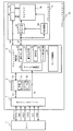
図10は、従来のフラッシュメモリカード100と情報処理機器(以下、ホストという)Hとによるデータ交換の一例を示すブロック図である。
フラッシュメモリカード100はホストHと、例えば、データラインDAT、クロックラインCLK、電源ラインVDD、グラウンドラインVSS及びコマンドラインCMDの5種類のラインで接続される。
【0010】
ホストインタフェース1はコマンドラインCMDを通じてホストHからコマンドを受信し、解読する。そのコマンドが例えばデータの書き込み命令である時、ホストインタフェース1は、データの書き込み先としてホストHにより指示された論理アドレスALをコマンドから解読し、フラッシュメモリ制御部30へ出力する。一方ホストインタフェース1は、書き込み対象のデータDaをデータラインDATから受信し、バッファ2へストアする。
【0011】
フラッシュメモリ制御部30では、アドレス変換部30aがデータDaの書き込み先の論理アドレスALをホストインタフェース1から入力する。
アドレス変換部30aは一つの論理アドレスに対して一般に、複数のエリアの物理アドレスを対応させる。ここで、一つのエリアは、フラッシュメモリ4のセルアレイ4b内の、例えば2ページに相当する。特に、同じエリアに属するページはそれぞれ異なる物理ブロックに属する。
【0012】
アドレス変換部30aは更に、同じ論理アドレスに対応する複数のエリアをそれぞれ、未記憶、有効及び無効の三つの状態に区別する。それぞれのエリアの状態に関する情報は、フラッシュメモリ4のそれぞれのページに付加された冗長領域に記憶される。ここで、冗長領域は一定数のメモリセルから成る。更に、同じエリアに属するページの冗長領域には、そのエリアの状態に関する共通の情報が記憶される。
未記憶の状態とは、データの消去後そのエリアにはまだデータが書き込まれていないことを表す。それに対して、有効と無効との状態は、データを書き込まれたエリアの状態である。有効又は無効の状態はそれぞれ、読み出し部30bによるそのエリアからのデータの読み出しが許可され又は禁止されていることを表す。
【0013】
データDaの書き込み先の論理アドレスALを入力した時、アドレス変換部30aはセルアレイ4b内から未記憶のエリアを選択し、データDaの書き込み先のエリアとして割り当てる。アドレス変換部30aは更に、そのエリアの物理アドレスAPを上記の論理アドレスALに対応させる。
【0014】
書き込み部30cは書き込み先のエリアの物理アドレスAPをフラッシュメモリ4のアドレスデコーダ4cへ出力する。それと共に、書き込み対象のデータDaをバッファ2からフラッシュメモリ4のページバッファ4aへ出力する。
フラッシュメモリ4はページバッファ4aを、例えば二つ有する。ページバッファ4aは一つ当たり1ページのデータをストアできる。つまり、二つのページバッファ4aは合わせて1エリアのデータをストアできる。従って、バッファ2から出力された書き込み対象のデータDaは1エリアずつ、ページバッファ4aへストアされる。
【0015】
二つのページバッファ4aにストアされた1エリアのデータは、アドレスデコーダ4cにより指定された2ページへ並列に書き込まれる。こうして、従来のフラッシュメモリカード100は、フラッシュメモリ4へのデータの書き込みを二つの物理ブロックに対して並列に実行する。それにより、データの書き込み時間を短縮する。
【0016】
データDaの書き込み先の論理アドレスALを入力した時、アドレス変換部30aは上記の動作と共に、その論理アドレスALに対応する物理アドレスの中から有効なエリアを探す。ホストにより指示されたデータの書き込みがデータの上書きである時、データDaの書き込み先の論理アドレスALに対応する物理アドレスのエリアの中に、有効なエリアが一般に存在する。その時、フラッシュメモリ制御部30内のページ無効化部30eがその有効なエリアを、次のように無効化する。それにより、読み出し部30bによるそのエリアへのアクセスが禁止される。
【0017】
ページ無効化部30eは、有効なページに対応する冗長領域内のデータを書き換え、それによりそのページを無効化する。例えば、冗長領域内の所定の1ビット(以下、フラグという)が「1」の時、そのページは有効であり、「0」の時無効である、と定義する。有効なページに対応するフラグは「1」であるので、ページ無効化部30eはそのフラグを「1」から「0」に遷移させる。すなわち、冗長領域のフラグに「0」を書き込む。それにより、そのページは無効化される。
【0018】
上記の通り、従来のフラッシュメモリカード100は、ホストからデータの上書きを指示された時、元のデータを消去せず、別のエリアへ新たなデータを書き込む。更に、新たなデータを書き込まれたエリアの物理アドレスをデータの書き込み先の論理アドレスに対応させる。その上、元のデータを記憶したエリアについて、その状態を無効にする。それにより、その論理アドレスを目標とするデータの読み出し命令をホストから受けた時、読み出し部30bはその論理アドレスに対応する複数のエリアの中で、最新のデータを記憶したエリアへアクセスする。こうして、同一の論理アドレスへのデータの上書きが、フラッシュメモリでのデータの消去を伴わずに実現される。それ故、データの上書き時間がデータの消去時間だけ短縮される。
【0019】
【発明が解決しようとする課題】
上記のような従来のフラッシュメモリ装置では、同一の論理アドレスへのデータの上書きごとに、元のデータを記憶した有効なエリアが無効化され、無効なエリアの数が増大した。従って、同一の論理アドレスへのデータの上書きが何度も繰り返される時、無効なエリアの数が有効なエリアに比べて著しく増大した。
【0020】
更に、フラッシュメモリでは物理ブロックごとに一括してのみ、データが消去される。それ故、従来のフラッシュメモリ装置では、消去目標の物理ブロック内に一つでも有効なエリアがあると、その物理ブロック内の多数の無効なエリアに対してデータの消去が実行され得なかった。従って、有効なエリアに対する無効なエリアの割合を低減できなかった。
以上の結果、従来のフラッシュメモリ装置では、データの上書きの繰り返しにより、フラッシュメモリへ記憶可能なデータ量がフラッシュメモリの記憶容量に比べて大きく減少した。
【0021】
本発明は、有効なページに対する無効なページの割合を低減し、それにより記憶可能なデータ量を増大したフラッシュメモリ装置、の提供を目的とする。
【0022】
【課題を解決するための手段】
本発明によるフラッシュメモリ装置は、
(A) (a) 一定の記憶容量、及び、(b) 未記憶と有効と無効との三つの状態、を持つページ、を複数含む物理ブロック、を複数有するフラッシュメモリ;
(B) 外部から入力した論理アドレスを、対応するページの物理アドレスの一つに変換するためのアドレス変換部;
(C) 有効なページからデータを読み出すための読み出し部;
(D) 未記憶のページごとにデータを書き込むための書き込み部;
(E) 物理ブロックごとに一括してデータを消去するための消去部;
(F) 有効なページを無効化するためのページ無効化部;並びに、
(G) (a) コピー元の物理ブロックを選択し、(b) 読み出し部と書き込み部とにより、コピー元の物理ブロックに属する所定数の有効なページのデータを未記憶のページへコピーする、ためのマージ制御部;
を具備する。
【0023】
ここで、ページの三つの状態はそれぞれ次のように定義される: 未記憶の状態とは、データの消去後そのページにはまだデータが書き込まれていないことを表す。それに対して、有効と無効との状態は、データを書き込まれたページの状態である。有効又は無効の状態はそれぞれ、読み出し部によるそのページからのデータの読み出しが許可され又は禁止されていることを表す。
【0024】
上記のフラッシュメモリ装置では特に、外部から入力した論理アドレスへのデータの上書きが、次のように実行される: データの書き込み時、アドレス変換部は上記の論理アドレスを未記憶のページの物理アドレスへ変換する。書き込み部はその物理アドレスのページへ、外部から入力した新たなデータを書き込む。一方、ページ無効化部が、元のデータを記憶した有効なページ、を無効化する。それにより、上記の論理アドレスからのデータの読み出し時、読み出し部は上記の無効化されたページに代えて、新たなデータを書き込まれたページへアクセスする。こうして、上記のフラッシュメモリ装置では、同一の論理アドレスへのデータの上書きが、データの消去を実行することなく実現される。それ故、データの消去に要する時間だけデータの上書き時間が短縮される。
【0025】
更に、上記のフラッシュメモリ装置では、マージ制御部が、所定の物理ブロックから有効なページのデータを読み出し部により読み出し、そのデータを別の未記憶のページへ書き込み部により書き込む。それにより、所定の物理ブロック内の有効なページのデータを他の物理ブロックへコピーできる。特に、所定の物理ブロック内の全ての有効なページのデータをコピーし終えた時、消去部によりその物理ブロックのデータを一括して消去する。以下、有効なページのデータのコピー、及び、それに続く物理ブロックのデータの消去を、マージ処理という。上記のフラッシュメモリ装置は従来の装置とは異なり、マージ処理により、有効なページを含む物理ブロックについて、その中の無効なページのデータを消去できる。従って、上記のフラッシュメモリ装置は、有効なページに対する無効なページの割合を低減できる。その結果、データの上書きの繰り返し時での記憶可能なデータ量が従来の装置より多い。
【0026】
上記のフラッシュメモリ装置は、次のことを特徴としても良い:
書き込み部による新たなデータの書き込み時、マージ制御部が、
(A) 未記憶のページのみを含む物理ブロック、の数をカウントし;
(B) 第一の閾値以下のカウント値を得た時、コピー元の物理ブロックを選択し;
(C) (a) コピー元の物理ブロックに属し、かつ、(b) 新たなデータを書き込まれるページの数と比べて少なくとも同数の有効なページ、をコピー元のページとして選択し;
(D) コピー元のページのデータを未記憶のページへコピーし;
(E) コピー元のページをページ無効化部により無効化し;
(F) 消去部により、有効なページを含まない物理ブロックについてデータの消去を実行する。
【0027】
もし新たなデータの書き込みごとにマージ処理を行うと、マージ処理の時間だけデータの書き込み時間が従来のフラッシュメモリ装置より長い。そこで、上記のフラッシュメモリ装置ではマージ制御部が、新たなデータの書き込み時、未記憶のページのみを含む物理ブロック(以下、消去済物理ブロックという)の数をカウントする。そのカウント値が第一の閾値より小さい時、すなわち、データの書き込み可能な領域が所定の大きさより狭い時、マージ制御部はマージ処理を実行する。こうして、マージ処理の実行時期の制限により、上記のフラッシュメモリ装置は、マージ処理によるデータの書き込み時間の延長を低減できる。
【0028】
更に、書き込み対象のデータ量は一般に、物理ブロックの整数倍程度の記憶容量に等しい。そこで、マージ制御部はコピー元のページの数を、新たなデータを書き込まれるページと比べて同数以上にする。それにより、同一の論理アドレスへのデータの上書き時、マージ処理により消去される物理ブロック数を、新たなデータの書き込みにより消費される消去済物理ブロック数と比べて同程度以上にできる。その結果、上記のフラッシュメモリ装置では、データの上書きの繰り返し時、有効なページに対する無効なページの割合の増大が回避される。
【0029】
上記のフラッシュメモリ装置は、次のことを特徴としても良い:
書き込み部による新たなデータの書き込み時、マージ制御部が、
(A) 未記憶のページのみを含む物理ブロック(消去済物理ブロック)の数をカウントし;
(B) 第二の閾値以下のカウント値を得た時、書き込み部に対して新たなデータの書き込みを禁止して、コピー元の物理ブロックを選択し;
(C) コピー元の物理ブロックに属する有効なページのデータを全て、コピー元の物理ブロックとは別の物理ブロックに属する未記憶のページへコピーし;
(D) 消去部により、コピー元の物理ブロックのデータを消去する。
【0030】
上記のフラッシュメモリ装置では、消去済物理ブロックの残数が第二の閾値以下である時、新たなデータの書き込みより優先してマージ処理が行われる。それにより、消去済物理ブロックの数を第二の閾値程度以上確保できるように、有効なページに対する無効なページの割合を低減する。その結果、上記のフラッシュメモリ装置では記憶可能なデータ量が増大し得る。
【0031】
消去済物理ブロックの残数が第一の閾値以下である時の上記の動作と、第二の閾値以下である時の上記の動作と、の両方を上記のフラッシュメモリ装置が行う時、第二の閾値は第一の閾値より小さい。それにより、新たなデータの書き込みができないほど消去済物理ブロックの数が少ない時に初めて、新たなデータの書き込みより優先してマージ処理が実行される。その結果、マージ処理によるデータの書き込み時間の延長を低減できる。
【0032】
上記のフラッシュメモリ装置が、物理ブロックのアドレスとその物理ブロックに属する無効なページの数とのリスト、を記憶するためのアドレスメモリ、を更に有しても良い。マージ制御部はコピー元の物理ブロックの選択時、アドレスメモリにアクセスし、上記のリストを参照する。それにより、無効なページを多く含む物理ブロックから順に、コピー元の物理ブロックを容易にかつ迅速に選択できる。その結果、データをコピーすべき有効なページの数が最小になるので、上記のマージ処理に要する時間を短縮できる。
【0033】
上記のフラッシュメモリ装置が、次のことを特徴としても良い:
(a) 異なる物理ブロックにそれぞれ属する所定数のページが一つのエリアに割り当てられ;
(b) 読み出し部が、同じエリアに属する複数の有効なページからデータをパラレルに読み出し;
(c) 書き込み部が、同じエリアに属する複数の未記憶のページへデータをパラレルに書き込み;かつ、
(d) ページ無効化部が、同じエリアに属する有効なページを全て無効化する。
【0034】
上記のフラッシュメモリ装置では、フラッシュメモリに対するデータの入出力が常に一つのエリアごとに、すなわち、複数のページずつ並列に実行される。従って、フラッシュメモリに対するデータの入出力を一つのページごとに行うフラッシュメモリ装置に比べて、処理速度が速い。
【0035】
上記のフラッシュメモリ装置が更に、次のことを特徴としても良い:
(a) そのフラッシュメモリ装置がフラッシュメモリを二つ以上有し;
(b) 読み出し部、書き込み部、消去部、ページ無効化部又はマージ制御部、の少なくとも二つが、それぞれ異なるフラッシュメモリに対して並列に動作する。
【0036】
上記のフラッシュメモリ装置では、例えば、一つのフラッシュメモリに対しては書き込み部が新たなデータの書き込みを行う。それと並行して、別のフラッシュメモリに対してはマージ制御部がマージ処理を行う。それにより、フラッシュメモリを一つだけ含むフラッシュメモリ装置に比べ、マージ処理によるデータの書き込み時間の延長を低減できる。
【0037】
本発明の一つの観点による、フラッシュメモリに記憶されたデータのマージ方法は、
(a) 一定の記憶容量、及び、(b) 未記憶と有効と無効との三つの状態、を持つページ、を複数含む物理ブロック、を複数有するフラッシュメモリ、に記憶されたデータのマージ方法であり、
(a) コピー元の物理ブロックを選択するステップ;
(b) コピー元の物理ブロックに属する所定数の有効なページのデータを、未記憶のページへコピーするステップ;及び、
(c) 物理ブロックごとにデータを消去するステップ;
を有する。
【0038】
上記のマージ方法では、所定の物理ブロック内の有効なページのデータを他の物理ブロックへコピーし、その物理ブロックのデータを一括して消去する。そのようなマージ処理により、有効なページを含む物理ブロックについて、その中の無効なページのデータを消去できる。それ故、上記のマージ方法では、有効なページに対する無効なページの割合を低減できる。その結果、フラッシュメモリへ記憶可能なデータ量が増大し得る。
【0039】
本発明の別の観点による、フラッシュメモリに記憶されたデータのマージ方法は、
(a) 一定の記憶容量、及び、(b) 未記憶と有効と無効との三つの状態、を持つページ、を複数含む物理ブロック、を複数有するフラッシュメモリ、に記憶されたデータのマージ方法であり、
(A) 未記憶のページのみを含む物理ブロック(消去済物理ブロック)、の数をカウントするステップ;
(B) そのカウント値を第一の閾値と比較するステップ;
(C) そのカウント値が第一の閾値以下である時、新たなデータの書き込みを実行し、その書き込み先のページの数を取得するステップ;
(D) コピー元の物理ブロックを選択するステップ;
(E) (a) コピー元の物理ブロックに属し、かつ、(b) 新たなデータの書き込み先のページの数と比べて少なくとも同数の有効なページ、をコピー元のページとして選択するステップ;
(F) コピー元のページのデータを、未記憶のページへコピーするステップ;
(G) コピー元のページを無効化するステップ;
(H) 有効なページを含まない物理ブロック、を消去目標物理ブロックとして選択するステップ;及び、
(I) 消去目標物理ブロックのデータを消去するステップ;
を有する。
【0040】
上記のマージ方法では、消去済物理ブロックの数が第一の閾値より小さい時、すなわち、データの書き込み可能な領域が所定の大きさより狭い時、マージ処理が実行される。従って、マージ処理の実行時期の制限により、マージ処理によるデータの書き込み時間の延長を低減できる。
【0041】
更に、書き込み対象のデータ量は一般に、物理ブロックの整数倍程度の記憶容量に等しい。上記のマージ方法では、コピー元のページの数が新たなデータの書き込み先のページと比べて同数以上である。従って、特に、同一の論理アドレスへのデータの上書き時、有効なページのデータのコピーにより消去可能となる物理ブロック数が、新たなデータの書き込みにより消費される消去済物理ブロック数と比べて同程度以上になり得る。その結果、上記のマージ方法では、データの上書きの繰り返し時、有効なページに対する無効なページの割合の増大を回避できる。
【0042】
本発明の更に別の観点による、フラッシュメモリに記憶されたデータのマージ方法は、
(a) 一定の記憶容量、及び、(b) 未記憶と有効と無効との三つの状態、を持つページ、を複数含む物理ブロック、を複数有するフラッシュメモリ、に記憶されたデータのマージ方法であり、
(A) 未記憶のページのみを含む物理ブロック(消去済物理ブロック)の数をカウントするステップ;
(B) そのカウント値を第二の閾値と比較するステップ;
(C) そのカウント値が第二の閾値以下である時、新たなデータの書き込みを禁止するステップ;
(D) コピー元の物理ブロックを選択するステップ;
(E) コピー元の物理ブロックに属する有効なページのデータを全て、コピー元のページとして選択するステップ;
(F) コピー元のページのデータを、コピー元の物理ブロックとは別の物理ブロックに属する未記憶のページへコピーするステップ;及び、
(G) コピー元の物理ブロックのデータを消去するステップ;
を有する。
【0043】
上記のマージ方法では、消去済物理ブロックの残数が第二の閾値以下である時、新たなデータの書き込みより優先してマージ処理が行われる。それにより、消去済物理ブロックの数を第二の閾値程度以上確保できるように、有効なページに対する無効なページの割合を低減する。その結果、上記のマージ方法では、フラッシュメモリへ記憶可能なデータ量が増大し得る。
【0044】
消去済物理ブロックの残数が第一の閾値以下である時の上記のマージ処理と、第二の閾値以下である時の上記のマージ処理と、の両方を上記のマージ方法が含む時、第二の閾値は第一の閾値より小さい。それにより、新たなデータの書き込みができないほど消去済物理ブロックの数が少ない時に初めて、新たなデータの書き込みよりマージ処理が優先して実行される。その結果、マージ処理によるデータの書き込み時間の延長を低減できる。
【0045】
上記のマージ方法では、コピー元の物理ブロックを選択するステップが、物理ブロックのアドレスとその物理ブロックに属する無効なページの数とのリスト、を参照するサブステップ、を有しても良い。それにより、無効なページを多く含む物理ブロックから順に、コピー元の物理ブロックを容易にかつ迅速に選択できる。その結果、データをコピーすべき有効なページの数が最小になるので、上記のマージ処理に要する時間を短縮できる。
【0046】
【発明の実施の形態】
以下、本発明の最適な実施の形態について、その好ましい実施例を挙げて、図面を参照しつつ説明する。
【0047】
《実施例1》
図1は、本発明の実施例1によるフラッシュメモリカード10とホストHとによるデータ交換を示すブロック図である。
フラッシュメモリカード10はホストHと、次の5種類のラインで接続される。それらのラインは、4本のデータラインDAT0〜3、クロックラインCLK、電源ラインVDD、2本のグラウンドラインVSS1、VSS2、及び、コマンドラインCMD、の合計9本から成る。
【0048】
ホストインタフェース1は、上記の9本のラインを通してホストHと直接通信を行うための回路である。ホストインタフェース1は、コマンドラインCMDを通じてホストHからのコマンドを受信し、解読する。その後、コマンドに応じて、例えば以下の処理を行う。
【0049】
ホストHからのコマンドがデータの読み出し命令である時、ホストインタフェース1は読み出し目標の論理アドレスALをコマンドから解読し、フラッシュメモリ制御部3へ出力する。
【0050】
ホストHからのコマンドがデータの書き込み命令である時、ホストインタフェース1は書き込み先の論理アドレスALをコマンドから解読し、フラッシュメモリ制御部3へ出力する。一方、ホストインタフェース1は、データラインDAT0〜3から書き込み対象のデータを、クロックラインCLKからの転送クロックに同期して読み出し、バッファ2へストアする。
【0051】
ホストHからのコマンドがデータの消去命令である時、ホストインタフェース1は消去目標の論理アドレスALをコマンドから解読し、フラッシュメモリ制御部3へ出力する。
【0052】
バッファ2は好ましくはSRAMであり、ホストインタフェース1とフラッシュメモリ制御部3との間で交換されるデータDaを一時記憶する。それにより、処理速度の相違、すなわち、ホストHからの転送クロックCLKとフラッシュメモリカード10の内部クロックとの周波数の相違に妨げられることなく、ホストインタフェース1とフラッシュメモリ制御部3とは互いにデータDaを交換できる。
その他に、バッファ2はホストインタフェース1とフラッシュメモリ制御部3とのそれぞれに対して、作業用メモリ領域を提供する。
【0053】
フラッシュメモリ4は好ましくはNAND型EEPROM(電気的消去及び書き込み可能不揮発性メモリ)であり、ページバッファ4a、セルアレイ4b、アドレスデコーダ4c及び消去回路4dを含む。
【0054】
図2はセルアレイ4bの構成を示す模式図である。
セルアレイ4bは複数の物理ブロックB0、B1、B2、・・・の集合である。それぞれの物理ブロックは多数のメモリセルを、次のように二次元的に配列したものである: NAND型に接続された8個のメモリセルを1列として、512列を1ページとする。更に、1ページごとに16列の冗長領域を付加する。1ページに冗長領域を付加した配列を1単位として、32単位を一つの物理ブロックとする。
例えば、第一の物理ブロックB0は32枚のページP0〜P31を含む。それぞれのページP0〜P31には16バイトの冗長領域Pr0〜Pr31が付加されている。同様に、第二の物理ブロックB1は32枚のページQ0〜Q31を含み、それぞれのページQ0〜Q31には冗長領域Qr0〜Qr31が付加されている。他の物理ブロックB2、B3、・・・についても同様である。
【0055】
一つのメモリセルは1ビットのデータを記憶するので、セルアレイ4bでは1列当たり8ビット=1バイト、1ページ当たり512バイト、1物理ブロック当たり512バイト×32=16KB、のデータがそれぞれ記憶される。更に、実施例1では、セルアレイ4bが物理ブロックを210=1024個だけ有するので、16KB×1024=16MBの記憶容量を有する。
【0056】
フラッシュメモリ4はページバッファ4aを、例えば二つ有する。ページバッファ4aは一つ当たり1ページのデータをストアできる。
セルアレイ4bへのデータの書き込み時、フラッシュメモリ制御部3からのデータDaは2×512バイトずつ二つのページバッファ4aへ一時記憶される。更に、それぞれのページバッファ4aからセルアレイ4b内の別々の2ページへ並列に書き込まれる。
セルアレイ4bからのデータの読み出し時、データがセルアレイ4b内の別々の2ページから並列に読み出され、二つのページバッファ4aのそれぞれへ一時記憶される。更に、二つのページバッファ4aから一連のデータDaとしてフラッシュメモリ制御部3へパラレルに転送される。
【0057】
データの書き込み先又は読み出し目標の2ページはそれぞれ、異なる物理ブロックから選択される。例えば、図2に斜線で示されている2ページ、すなわち、第一の物理ブロックB0と第二の物理ブロックB1とのそれぞれの第一のページPOとQ0とが選択される。同様に、奇数番目の物理ブロックと偶数番目の物理ブロックとのそれぞれ一つずつから、対応する位置のページが一つずつ選択される。その時の選択はアドレスデコーダ4cにより、フラッシュメモリ制御部3から入力した物理アドレスAPに従って行われる。以下、そのように選択されるセルアレイ4b内の2ページの対を1エリアという。
【0058】
消去回路4dは、フラッシュメモリ制御部3から入力した物理アドレスAPに対応する物理ブロックに高電圧を印加し、それにより、その物理ブロック内に記憶されているデータを一括して消去する。その時、物理ブロックごとにデータの消去が実行されるように、セルアレイ4b内の物理ブロックはそれぞれ互いに電気的に絶縁されている。
【0059】
フラッシュメモリ制御部3は、以下に述べる各構成要素により、フラッシュメモリ4に対するデータの入出力制御を行う。
アドレス変換部3aはホストインタフェース1から論理アドレスALを入力する。更に、フラッシュメモリ4のセルアレイ4bの中からその論理アドレスALに対応するエリアを選択し、論理アドレスALをそのエリアの物理アドレスAPへ変換する。
アドレス変換部3aは一つの論理アドレスALに対して一般に、複数のエリアの物理アドレスAPを対応させる。更に、同じ論理アドレスALに対応する複数のエリアをそれぞれ、未記憶、有効及び無効の三つの状態に区別し、それぞれの状態に応じてそのエリアの物理アドレスAPを選択する。
【0060】
未記憶の状態とは、データの消去後そのエリアにはまだデータが書き込まれていないことを表す。それに対して、有効と無効との状態は、データを書き込まれたエリアの状態である。有効又は無効の状態はそれぞれ、読み出し部3bによるそのエリアからのデータの読み出しが許可し又は禁止されていることを表す。
【0061】
それぞれのエリアの状態に関する情報は、フラッシュメモリ4のそれぞれのページに付加された冗長領域(例えば、ページP0に対応する冗長領域Pr0等)に記憶される。特に、同じエリアに属するページの冗長領域には、そのエリアの状態に関する共通の情報が記憶される。
【0062】
アドレス変換部3はフラッシュメモリカード10の起動時、フラッシュメモリ4のセルアレイ4b内の全エリアの状態をチェックする。更に、それぞれのエリアの状態についてのテーブル(以下、状態テーブルという)2aを、バッファ2内に作成する。状態テーブル2aは例えば、エリアの物理アドレス、そのエリアに対応する論理アドレス、及び、そのエリアの状態についての情報、のリストである。
【0063】
論理アドレスALがデータの読み出し目標を示す時、アドレス変換部3aは状態テーブル2aを参照し、その論理アドレスALに対応するセルアレイ4b内のエリアの中から、有効なエリアを選択する。読み出し部3bはその有効なエリアの物理アドレスAPをフラッシュメモリ4へ出力する。フラッシュメモリ4へ入力された物理アドレスAPは、アドレスデコーダ4cにより解読される。それにより、その物理アドレスAPに対応するセルアレイ4b内のエリアに属するそれぞれのページから二つのページバッファ4aへ、データが並列に読み出される。読み出し部3bはページバッファ4aからバッファ2へ、データDaを転送する。
【0064】
論理アドレスALがデータの書き込み先を示す時、アドレス変換部3aは状態テーブル2aを参照し、セルアレイ4b内から未記憶のエリアを選択する。更に、それらの未記憶のエリアの物理アドレスAPを、書き込み先の論理アドレスALに対応させる。書き込み部3cは書き込み対象のデータDaを、バッファ2からフラッシュメモリ4内のページバッファ4aへ、2×512バイトずつ転送する。それと共に、アドレス変換部3aにより選択された未記憶のエリアの物理アドレスAPをフラッシュメモリ4へ出力する。フラッシュメモリ4へ入力された物理アドレスAPはアドレスデコーダ4cにより解読される。それにより、その物理アドレスAPに対応するセルアレイ4b内のエリアに属するページのそれぞれへ、別々のページバッファ4aからデータが並列に書き込まれる。更に、データの書き込みの終了時、アドレス変換部3は状態テーブル2aを更新し、書き込み先のエリアの状態についての項目を未記憶から有効へと書き換える。
【0065】
上記の通り、フラッシュメモリ4に対するデータの書き込み及び読み出しは、二つのページバッファ4aを通して1エリアごとに、すなわち、異なる二つの物理ブロックの1ページずつへ並列に行われる。こうして、実施例1によるフラッシュメモリカード10は、フラッシュメモリ4に対するデータの書き込み時間及び読み出し時間を短縮する。
【0066】
論理アドレスALがデータの消去目標を示す時、アドレス変換部3aはその論理アドレスALに対応する物理ブロックの物理アドレスAPを特定する。消去部3dは、アドレス変換部3aにより特定された消去目標の物理アドレスAPを、フラッシュメモリ4内の消去回路4dへ出力する。消去回路4dはアドレスデコーダ4cを停止し、入力した物理アドレスAPに対応する物理ブロックへ所定の高電圧を印加する。それにより、その物理ブロックに対するデータの消去が実行される。更に、データの消去の終了時、アドレス変換部3は状態テーブル2aを更新し、消去目標の物理ブロック内の全エリアの状態についての項目を有効へ書き換える。
【0067】
データの書き込み時、アドレス変換部3aは上記の動作と共に状態テーブル2aを参照し、書き込み先の論理アドレスALに対応する物理アドレスのエリアの中から有効なエリアを探す。ホストHにより指示された書き込みがデータの上書きである時、論理アドレスALに対応する物理アドレスのエリアの中には、有効なエリアが一般に存在する。その時、ページ無効化部3eがその有効なエリアを次のように無効化する。更に、アドレス変換部3が状態テーブル2aを更新し、そのエリアの状態についての項目を有効から無効へと書き換える。それにより、読み出し部3bによるそのエリアへのアクセスが禁止される。
【0068】
ページ無効化部3eは、有効なページに対応する冗長領域内のデータを書き換える。それにより、そのページを無効化する。例えば、冗長領域内の所定の1ビット(フラグ)が「1」の時そのページは有効であり、「0」の時無効である、と定義する。有効なページに対応するフラグは「1」であるので、ページ無効化部3eはそのフラグを「1」から「0」に遷移させる。すなわち、冗長領域内のフラグに「0」を書き込む。それにより、そのページは無効化される。
【0069】
上記の通り、実施例1によるフラッシュメモリカード10は、ホストHからデータの上書きを指示された時、元のデータを消去せず、別のエリアへ新たなデータを書き込む。更に、新たなデータを書き込まれたエリアの物理アドレスをデータの書き込み先の論理アドレスに対応させる。その上、その論理アドレスに対応する他の物理アドレスのエリアについて、その状態を無効にする。それにより、その論理アドレスを目標とするデータの読み出し命令をホストから受けた時、読み出し部3bはその論理アドレスに対応する複数のエリアの中で、最新のデータを記憶したエリアへのみアクセスできる。こうして、同一の論理アドレスへのデータの上書きが、フラッシュメモリ4でのデータの消去を伴わずに実現される。それ故、データの上書き時間がデータの消去時間だけ短縮される。
【0070】
実施例1によるフラッシュメモリカード10はフラッシュメモリ制御部3内に更に、マージ制御部3fを有する。
上記の通り、データの上書きは無効なページを生成する。従って、データの上書きを繰り返すと、有効なエリアに対する無効なエリアの割合が増大する。マージ制御部3fは、読み出し部3b、書き込み部3c、消去部3d及びページ無効化部3eを以下に述べるように制御する。それにより、所定の物理ブロック内の有効なページのデータを別の物理ブロック内の未記憶のページへコピーする。更に、元の物理ブロックのデータを消去し、未記憶のページのみを含む物理ブロック(消去済物理ブロック)の数を増やす。その結果、有効なエリアに対する無効なエリアの割合を低減できる。
【0071】
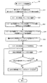
図3はマージ制御部3fの動作についてのフローチャートである。
マージ制御部3fはフラッシュメモリ4へのデータの書き込み時に起動する。
ステップS1:
マージ制御部3fはバッファ2内の状態テーブル2aを参照し、消去済物理ブロックの数Nをカウントする。
ステップS2:
ステップS1でカウントされた消去済物理ブロック数Nを、第一の閾値th1と第二の閾値th2とそれぞれ比較する。ここで、第一の閾値th1及び第二の閾値th2はそれぞれ、セルアレイ4b内の全物理ブロック数の、例えば、約50%及び約20%に等しい。
更に、上記の比較の結果に依存して、マージ制御部3fは以下のように処理を分岐する: (1) 消去済物理ブロック数Nが第一の閾値th1以上である時(N≧th1)、マージ制御部3fは停止する。(2) 消去済物理ブロック数Nが第一の閾値th1より小さく第二の閾値th2以上である時(th2≦N<th1)、マージ制御部3fは第一のマージ処理S3を実行する。(3) 消去済物理ブロック数Nが第二の閾値th2より小さい時(N<th2)、マージ制御部3fは第二のマージ処理S4を実行する。
【0072】
ステップS1及びステップS2により、消去済物理ブロック数Nが第一の閾値th1より小さい時のみ、すなわち、データの書き込み可能な領域が残り少ない時のみ、マージ制御部3fは以下のマージ処理を実行する。こうして、実施例1によるフラッシュメモリカード10では、マージ処理によるデータの書き込み時間の延長を制限する。
【0073】
<第一のマージ処理S3>
図4は第一のマージ処理S3についてのフローチャートである。
図5は第一のマージ処理S3時、セルアレイ4b内のページの状態の変化を示す模式図である。実施例1では、奇数番目の物理ブロックの一つと、偶数番目の物理ブロックの一つと、の対応するページ同士は同じエリアに属する。更に、データの入出力はエリアごとにパラレルに行われる。従って、ページの状態の変化は、奇数番目の物理ブロックと偶数番目の物理ブロックとで実質上共通である。それ故、図5では、セルアレイ4b内の奇数番目の物理ブロックだけが示されている。
【0074】
図5では、それぞれのエリアP0、P1、P2、・・・に記憶されたデータが、それぞれのエリアを示す四角形内に書かれた符号D0、D1、D2、・・・で表される。その上、それぞれのエリアの状態が、対応する冗長領域Pr0、Pr1、Pr2、・・・を示す四角形内に書かれた数字1又は0で表される。ここで、数字1又は0はそれぞれ有効又は無効の状態を示す。更に、それぞれのエリアを示す四角形が空白の時、そのエリアの状態は未記憶である。
【0075】
サブステップS31:
図5の(a)に示されているように、新たなデータ(例えばd1、d2及びd3)が未記憶のエリアに書き込まれる。その時、マージ制御部3fは、新たなデータを書き込まれた未記憶のエリアの数k(例えば3)を取得する。
【0076】
サブステップS32:
マージ制御部3fはバッファ2内のアドレステーブル2bを参照し、無効なエリアを最も多く含む物理ブロックから順に、コピー元の物理ブロックBLを選択する。ここで、アドレステーブル2bは、物理ブロックのアドレスとその物理ブロックに属する無効なページの数とのリストである。例えば、図5の(a)では先頭の物理ブロックBLがコピー元の物理ブロックとして選択されている。
【0077】
サブステップS33:
マージ制御部3fはバッファ2内の状態テーブル2aを参照し、コピー元の物理ブロックBLの先頭エリアP0から順に有効なエリアを、サブステップS31で取得したエリア数と同数、すなわち、kエリアだけ選択する。例えば、図5の(a)では、有効な3エリアP0、P1及びP3が選択される。
ここで、コピー元の物理ブロックBL内の有効なエリアの数がkより小さい時、サブステップS32を再実行して別の物理ブロックをコピー元の物理ブロックとして選択し、その物理ブロックから残りの有効なエリアを選択する。
【0078】
サブステップS34:
マージ制御部3fはバッファ2内の状態テーブル2aを参照し、コピー元の物理ブロックBLとは別の物理ブロックから未記憶のエリアを、サブステップS31で取得したエリア数と同数、すなわち、kエリアだけ選択する。例えば、図5の(a)では未記憶の3エリアCP0、CP1及びCP3が選択される。
【0079】
サブステップS35:
マージ制御部3fは読み出し部3bにより、サブステップS33で選択された有効なエリアからデータを読み出す。読み出されたデータは、バッファ2へ一時記憶する。更に、マージ制御部3fは書き込み部3cにより、バッファ2へ一時記憶したデータを、サブステップS34で選択された未記憶のエリアへそれぞれ書き込む。こうして、コピー元の物理ブロックBL内の有効なkエリアのデータが、別の物理ブロックの未記憶のエリアへそれぞれコピーされる。例えば、図5の(a)では、コピー元の物理ブロックBL内の有効な3エリアP0、P1及びP3のデータD0、D1及びD3がそれぞれ、未記憶の3エリアCP0、CP1及びCP3へコピーされる。
【0080】
サブステップS36:
マージ制御部3fはページ無効化部3eにより、コピー元の物理ブロックBL内の有効なkエリアを無効化する。例えば、図5の(b)では、コピー元の物理ブロックBL内の有効な3エリアP0、P1及びP3に対応する冗長領域Pr0、Pr1及びPr3のデータが「1」から「0」へ書き換えられる。
更に、マージ制御部3fはバッファ2内の状態テーブル2aを更新し、コピー元の物理ブロックBL内の有効なkエリアの状態についての項目を、有効から無効へ書き換える。それに加えて、マージ制御部3fは更新された状態テーブル2aに基づいて、バッファ2内のアドレステーブル2bを更新する。
【0081】
サブステップS37:
マージ制御部3fはバッファ2内の状態テーブル2aを参照し、無効なエリアのみ又は多数の無効なエリアと少数の未記憶のエリアとのみを含む物理ブロック、を選択し、消去目標物理ブロックBEとする。例えば、図5の(c)では、先頭の物理ブロックBE内の全エリアの状態が無効であるので、その物理ブロックBEが消去目標として選択される。
【0082】
サブステップS38:
サブステップS37で消去目標物理ブロックBEが選択できたかどうか、をチェックする。消去目標物理ブロックBEが有る時、マージ制御部3fは処理をサブステップS39へ分岐し、それ以外の時、第一のマージ処理S3を終了する。
【0083】
サブステップS39:
マージ制御部3fは消去部3dにより、消去目標物理ブロックBEに対してデータの消去を実行する。例えば、図5の(d)では、消去目標物理ブロックBE内のエリアを示す四角形が全て空白で描かれ、全エリアの状態が未記憶に遷移したことを表している。データの消去の終了後、マージ制御部3fはバッファ2内の状態テーブル2aを更新し、消去目標物理ブロックBE内の全エリアの状態についての項目を有効へ書き換える。それに加えて、マージ制御部3fは更新された状態テーブル2aに基づいて、バッファ2内のアドレステーブル2bを更新する。その上で、マージ制御部3fは処理をサブステップS37から繰り返す。
【0084】
上記の通り、消去済物理ブロック数Nが第一の閾値th1より小さい時、第一のマージ処理S3はデータの書き込みごとに実行される。書き込み対象のデータ量は一般に、物理ブロックの整数倍程度の記憶容量に等しい。一方、マージ制御部3fはサブステップS33で有効なエリアを、新たなデータを書き込まれるエリアと同数だけ選択する。従って、特に同一の論理アドレスへのデータの上書き時、第一のマージ処理S3により消去可能となる物理ブロック数を一般に、新たなデータの書き込みにより消費される消去済物理ブロック数と同程度にできる。その結果、実施例1によるフラッシュメモリカード10では、データの上書きの繰り返し時、有効なエリアに対する無効なエリアの割合の増大を抑制できる。
【0085】
<第二のマージ処理S4>
図6は第二のマージ処理S4についてのフローチャートである。
図7は第二のマージ処理S4時、セルアレイ4b内のページの状態の変化を示す模式図である。図7では図5と同様、セルアレイ4b内の奇数番目の物理ブロックだけが示されている。更に、エリアに記憶されたデータ及びエリアの状態は図5と同様な符号で表されている。
【0086】
サブステップS41:
マージ制御部3fは第一のマージ処理S3時とは異なり、書き込み部3cに対して新たなデータの書き込みを禁止する。
【0087】
サブステップS42:
マージ制御部3fは第一のマージ処理S3のサブステップS32と同様に、バッファ2内のアドレステーブル2bを参照し、無効なエリアを最も多く含む物理ブロックから順に、コピー元の物理ブロックBLを選択する。例えば、図7の(a)では先頭の物理ブロックBLがコピー元の物理ブロックとして選択されている。
【0088】
サブステップS43:
マージ制御部3fはバッファ2内の状態テーブル2aを参照し、コピー元の物理ブロックBL内の有効なエリアを全て選択する。例えば、図7の(a)では、物理ブロックBL内の全ての有効なエリアP0及びP3が選択される。
【0089】
サブステップS44:
マージ制御部3fはバッファ2内の状態テーブル2aを参照し、コピー元の物理ブロックBLとは別の物理ブロックから未記憶のエリアを、サブステップS43で選択された有効なエリアの数と同数だけ選択する。例えば、図7の(a)では消去済物理ブロックの一つBn内の先頭の2エリアCP0及びCP1が選択される。
【0090】
サブステップS45:
マージ制御部3fは読み出し部3bにより、サブステップS43で選択された有効なエリアからデータを読み出す。読み出されたデータは、バッファ2へ一時記憶する。更に、マージ制御部3fは書き込み部3cにより、バッファ2へ一時記憶したデータを、サブステップS44で選択された未記憶のエリアへそれぞれ書き込む。こうして、コピー元の物理ブロックBL内の全ての有効なエリアのデータが、別の物理ブロックの未記憶のエリアへそれぞれコピーされる。例えば、図7の(a)では、コピー元の物理ブロックBL内の有効なエリアP0及びP3のデータD0及びD3がそれぞれ、消去済物理ブロックBnの未記憶の2エリアCP0及びCP1へコピーされる。
【0091】
サブステップS46:
マージ制御部3fは図7の(b)に示されているように、コピー元の物理ブロックBLを消去目標物理ブロックBEとして選択する。更に、消去部3dにより、消去目標物理ブロックBEに対するデータの消去を実行する。例えば、図7の(c)では、消去目標物理ブロックBE内のエリアを示す四角形が全て空白で描かれ、全エリアの状態が未記憶に遷移したことを表している。
データの消去の終了後、マージ制御部3fはバッファ2内の状態テーブル2aを更新し、消去目標物理ブロックBE内の全エリアの状態についての項目を有効へ書き換える。それに加えて、マージ制御部3fは、更新された状態テーブル2aに基づいて、バッファ2内のアドレステーブル2bを更新する。
【0092】
上記の通り、消去済物理ブロック数Nが第二の閾値th2より小さい時、第二のマージ処理S4が実行される。その時、新たなデータの書き込みは禁止され、サブステップS42〜S46による消去済物理ブロック数Nの増加が優先的に行われる。それにより、第二の閾値th2以上の消去済物理ブロック数Nが確保されるように、有効なエリアに対する無効なエリアの割合が低減される。その結果、実施例1によるフラッシュメモリカード10では、記憶可能なデータ量が増大する。
【0093】
実施例1では、フラッシュメモリ4がページバッファ4aを二つ有した。その他に、フラッシュメモリはページバッファを一つだけ、又は、三つ以上有しても良い。
【0094】
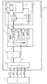
《実施例2》
図8は、本発明の実施例2によるフラッシュメモリカード10AとホストHとによるデータ交換を示すブロック図である。実施例2によるフラッシュメモリカード10Aは実施例1のもの10(図1)とは異なり、フラッシュメモリを二つ有する。図8では、実施例1と同様な構成要素については実施例1と同じ符号を付している。更に、それらの同様な構成要素についての説明は、実施例1のものを援用する。
【0095】
実施例2によるフラッシュメモリ制御部3A、及び、二つのフラッシュメモリ4Aと4Bとのそれぞれの内部構成は、図1に示されている実施例1のもの3及び4とそれぞれ全く同様であるので、それらについては図1を援用する。
【0096】
フラッシュメモリ制御部3Aとフラッシュメモリ4A又は4B内のページバッファ4aとの間でのデータ転送時間は数十nsec程度である。一方、ページバッファ4aからセルアレイ4bへのデータの書き込み時間は数百nsec程度である。それぞれの処理時間の違いを利用して、実施例2によるフラッシュメモリ制御部3Aは以下のように、一方のフラッシュメモリへのデータの書き込みと、他方のフラッシュメモリでのマージ処理と、を並列に実行する。それにより、マージ処理によるデータの書き込み時間の延長を、実施例1によるフラッシュメモリカード10に比べて低減できる。
【0097】
例えば、第一のフラッシュメモリ4Aへのデータの書き込み時、フラッシュメモリ制御部3A内の書き込み部3cは実施例1と同様に、第一のフラッシュメモリ4Aへ書き込み対象のデータDaを1エリアずつ転送する。その1エリアの転送ごとにフラッシュメモリ制御部3A内のマージ制御部3fが起動し、第二のフラッシュメモリ4Bに対して実施例1と同様に、ステップS1及びステップS2を実行する。マージ制御部3fは更に実施例1と同様に、ステップS2での比較の結果に応じて、第一のマージ処理S3又は第二のマージ処理S4を実行する。
【0098】
<第一のマージ処理S3>
実施例2による第一のマージ処理S3では実施例1とは異なり、サブステップS31でマージ制御部3fが、新たなデータを書き込まれた第一のフラッシュメモリ4A内のエリアの数を取得する。サブステップS33では、第二のフラッシュメモリ4B内のコピー元の物理ブロックから有効なエリアが、新たなデータを書き込まれた第一のフラッシュメモリ4A内のエリアの数と同数だけ選択される。それにより第一のフラッシュメモリ4Aへの1エリアのデータの書き込みと並列して、第二のフラッシュメモリ4Bの1エリアが別のエリアへコピーされる。更に、第一のフラッシュメモリ4Aでのデータの書き込み先のエリア数と、第二のフラッシュメモリ4Bで第一のマージ処理S3の対象となるエリア数と、が等しい。従って、第一のフラッシュメモリ4Aへのデータの書き込み時間と、第二のフラッシュメモリ4Bでの第一のマージ処理S3に要する時間と、がほぼ等しい。以上の結果、実施例2では実施例1と比べ、第一のマージ処理S3によるデータの書き込み時間の延長を低減できる。
【0099】
<第二のマージ処理S4>
実施例2による第二のマージ処理S4では実施例1とは異なり、マージ制御部3fが、第一のフラッシュメモリ4Aへのデータの書き込みを許可する。それにより第一のフラッシュメモリ4Aへのデータの書き込みと、第二のフラッシュメモリ4Bでの第二のマージ処理S4と、が並列して実行できる。それ故、実施例2では実施例1と比べ、第二のマージ処理S4によるデータの書き込み時間の延長を低減できる。
【0100】
《実施例3》
図9は、本発明の実施例3によるフラッシュメモリカード10BとホストHとによるデータ交換を示すブロック図である。実施例3によるフラッシュメモリカード10Bは実施例2のもの10A(図8)と同様に、フラッシュメモリを二つ有する。図9では、実施例1と同様な構成要素については実施例1と同じ符号を付している。更に、それらの同様な構成要素についての説明は、実施例1のものを援用する。
【0101】
実施例3による二つのフラッシュメモリ4Aと4Bとのそれぞれの内部構成は、図1に示されている実施例1のもの4とそれぞれ全く同様であるので、それらについては図1を援用する。
【0102】
実施例3によるフラッシュメモリ制御部3Bは、実施例1によるもの3と同様な内部構成を実質的に二重に含む。実施例1によるフラッシュメモリ制御部3と同様な内部構成の内、一方は第一のフラッシュメモリ4Aへ、他方は第二のフラッシュメモリ4Bへ、それぞれ別々に接続されている。更に、それぞれの内部構成とバッファ2Bとは別々のデータバスで接続されている。そのような構成により、実施例3によるフラッシュメモリカード10Bでは実施例2と同様に、二つのフラッシュメモリ4A及び4Bに対して、データの書き込みとマージ処理とを並列に実行できる。特に、実施例2とは異なり、バッファ2Bとフラッシュメモリ制御部3Bとの間でのデータ転送、及び、フラッシュメモリ制御部3Bとフラッシュメモリ4A又は4Bとの間でのデータ転送、も並列に実行される。従って、実施例2と比べてデータ転送時間だけ更に、データの書き込み時間を短縮できる。
【0103】
【発明の効果】
上記のように、本発明によるフラッシュメモリ装置は、所定の物理ブロック内の有効なページのデータを他の物理ブロックへコピーできる。更に、所定の物理ブロック内の全ての有効なページのデータをコピーし終えた時、その物理ブロックのデータを一括して消去できる。そのようなマージ処理により、本発明によるフラッシュメモリ装置は従来の装置とは異なり、有効なページを含む物理ブロックについて、その中の無効なページのデータを消去できる。従って、本発明によるフラッシュメモリ装置は、有効なページに対する無効なページの割合を低減できる。その結果、データの上書きの繰り返し時での記憶可能なデータ量が従来の装置より多い。
【0104】
本発明によるフラッシュメモリ装置は更に、新たなデータの書き込み時で、かつ、消去済物理ブロックの数が第一の閾値より小さい時、上記のマージ処理を実行しても良い。こうして、上記のフラッシュメモリ装置は、マージ処理の実行時期の制限により、データのコピーによるデータの書き込み時間の延長を低減できる。
【0105】
本発明によるフラッシュメモリ装置はコピー元のページの数を、新たなデータを書き込まれるページと比べて同数以上にしても良い。それにより、同一の論理アドレスへのデータの上書き時、上記のマージ処理により消去される物理ブロック数を、新たなデータの書き込みにより消費される消去済物理ブロック数と同程度以上にできる。その結果、データの上書きの繰り返し時、有効なページに対する無効なページの割合の増大を回避できる。それ故、記憶可能なデータ量を増大できる。
【0106】
本発明によるフラッシュメモリ装置では、消去済物理ブロックの数が第二の閾値以下である時、新たなデータの書き込みより優先して、上記のマージ処理が行われても良い。それにより、消去済物理ブロックの数を第二の閾値程度以上確保できるように、有効なページに対する無効なページの割合を低減できる。その結果、記憶可能なデータ量を増大できる。
【0107】
消去済物理ブロックの数が第一の閾値以下である時の動作と、第二の閾値以下である時の動作と、の両方を上記のフラッシュメモリ装置が行う時、第二の閾値は第一の閾値より小さい。それにより、新たなデータの書き込みができないほど消去済物理ブロックの数が少ない時に初めて、新たなデータの書き込みよりマージ処理が優先して実行される。その結果、マージ処理によるデータの書き込み時間の延長を低減できる。
【0108】
本発明によるフラッシュメモリ装置が、物理ブロックのアドレスとその物理ブロックに属する無効なページの数とのリストを有しても良い。上記のマージ処理では、コピー元の物理ブロックの選択時、上記のリストが参照される。それにより、コピー元の物理ブロックが、無効なページを最も多く含む物理ブロックから順に、容易にかつ迅速に選択される。その結果、上記のマージ処理の対象となる有効なページの数が最小になるので、上記のマージ処理に要する時間が短縮される。
【図面の簡単な説明】
【図1】本発明の実施例1によるフラッシュメモリカード10とホストHとによるデータ交換を示すブロック図である。
【図2】本発明の実施例1によるフラッシュメモリ4内のセルアレイ4bの構成を示す模式図である。
【図3】本発明の実施例1によるマージ制御部3fの動作についてのフローチャートである。
【図4】本発明の実施例1によるマージ制御部3fの動作の内、第一のマージ処理S3についてのフローチャートである。
【図5】本発明の実施例1による第一のマージ処理S3時、フラッシュメモリ4内のページの状態の変化を示す模式図である。
【図6】本発明の実施例1によるマージ制御部3fの動作の内、第二のマージ処理S4についてのフローチャートである。
【図7】本発明の実施例1による第二のマージ処理S4時、フラッシュメモリ4内のページの状態の変化を示す模式図である。
【図8】本発明の実施例2によるフラッシュメモリカード10AとホストHとによるデータ交換を示すブロック図である。
【図9】本発明の実施例3によるフラッシュメモリカード10BとホストHとによるデータ交換を示すブロック図である。
【図10】従来のフラッシュメモリカード100とホストHとによるデータ交換の一例を示すブロック図である。
【符号の説明】
10 フラッシュメモリカード
4a ページバッファ
Da フラッシュメモリ4に対して入出力されるデータ
AL ホストHから指示された論理アドレス
AP 論理アドレスALに対応する物理アドレス
DAT0〜3 データライン
CLK クロックライン
VDD 電源ライン
VSS1、2 グランドライン
CMD コマンドライン[0001]
BACKGROUND OF THE INVENTION
The present invention relates to a flash memory device having a flash memory, and more particularly to a method of merging data stored in each flash memory.
[0002]
[Prior art]
Portable information processing devices such as notebook personal computers, personal digital assistants (PDAs), and digital cameras record a large amount of digital data such as image data on an internal recording medium. The recording medium preferably has a large recording capacity, a small size and a light weight.
In particular, a portable information processing device such as a digital video camera (DVC) or an audio player records or reproduces a large amount of data on a recording medium in real time. Therefore, it is desirable that the recording medium is capable of processing a large amount of data at high speed.
Furthermore, the portable information processing device is used only for an extended time with an internal power source such as a battery. Accordingly, it is desirable that the recording medium has a low power consumption when inputting / outputting and holding data.
In addition, data handled by the portable information processing device is exchanged between various other information processing devices. For example, image data captured by a digital still camera (DSC) is printed by a printer, digitally processed by a personal computer, transmitted by a mobile phone, or displayed on a television screen. Therefore, it is desirable that the above recording medium can be shared among various information processing devices.
[0003]
As a recording medium that meets the above requirements, semiconductor memories are frequently used together with conventional flexible disks, hard disks, optical disks, and the like. In particular, a card-type recording medium with a built-in flash memory (hereinafter referred to as a flash memory card) such as a PC card is typical.
The flash memory card is inserted into a dedicated slot of the information processing device, and exchanges data with the information processing device. The dedicated slot follows a predetermined standard for flash memory cards. Information processing devices having the dedicated slot can exchange data through the same flash memory card.
[0004]
Unlike a RAM, a flash memory can hold data once stored for a long time without power consumption. Furthermore, unlike ROM, data can be rewritten electrically. In these respects, the flash memory is more advantageous as the recording medium than the RAM and ROM.
[0005]
In general, the flash memory is divided into a plurality of pages for each fixed number of memory cells, and further divided into a plurality of physical blocks for each fixed number of pages. Each memory cell can take two states, “1” and “0”. Thereby, one memory cell can store 1-bit data.
[0006]
A memory cell of a flash memory has the following characteristics regarding a transition between two states of “1” and “0”, for example, a NAND flash memory has the following characteristics: One memory cell in a “1” state is “0” one by one It is possible to transition to On the other hand, the memory cells in the “0” state can transition to the “1” state only when all the cells belonging to the same physical block are collectively displayed.
Therefore, the data stored in the flash memory can be erased only for each physical block. Here, erasing data means initializing all memory cells in the physical block to a state of “1”.
On the other hand, data can be written to the flash memory only for pages from which data has been erased. Here, the data writing means that some of the memory cells in the “1” state are changed to the “0” state.
[0007]
The flash memory cannot overwrite new data on a page that already stores data. This is because, for example, in a NAND flash memory, a memory cell in a “0” state cannot be individually transitioned to a “1” state. Therefore, when another data is overwritten on the same page, the data of the entire physical block including the page must be erased in advance. Therefore, the data overwrite time to the flash memory is generally longer than the RAM by the data erase time.
[0008]
For example, Japanese Patent Laid-Open No. 6-301601 discloses a storage device that writes data to a flash memory at high speed. Like the storage device, the conventional flash memory device writes data in parallel to a plurality of flash memories or a plurality of physical blocks. Thereby, the data writing time is shortened.
[0009]
FIG. 10 is a block diagram showing an example of data exchange between a conventional
The
[0010]
The
[0011]
In the flash
The
[0012]
The
The unstored state represents that data has not yet been written to the area after the data is erased. On the other hand, the valid and invalid states are states of the area where data is written. The valid or invalid state indicates that reading of data from the area by the reading unit 30b is permitted or prohibited.
[0013]
When the logical address AL of the data Da write destination is input, the
[0014]
The
The flash memory 4 has, for example, two
[0015]
The data of one area stored in the two
[0016]
When the logical address AL to which the data Da is written is input, the
[0017]
The
[0018]
As described above, the conventional
[0019]
[Problems to be solved by the invention]
In the conventional flash memory device as described above, every time data is overwritten to the same logical address, the valid area storing the original data is invalidated, and the number of invalid areas increases. Therefore, when overwriting data to the same logical address is repeated many times, the number of invalid areas is remarkably increased as compared with valid areas.
[0020]
Further, in the flash memory, data is erased only in batches for each physical block. Therefore, in the conventional flash memory device, if even one effective area exists in the physical block to be erased, data cannot be erased from a number of invalid areas in the physical block. Therefore, the ratio of the invalid area to the effective area cannot be reduced.
As a result, in the conventional flash memory device, the amount of data that can be stored in the flash memory is greatly reduced compared to the storage capacity of the flash memory due to repeated data overwriting.
[0021]
An object of the present invention is to provide a flash memory device that reduces the ratio of invalid pages to valid pages, thereby increasing the amount of data that can be stored.
[0022]
[Means for Solving the Problems]
A flash memory device according to the present invention comprises:
A flash memory having a plurality of physical blocks including: (A) (a) a fixed storage capacity; and (b) a page having a plurality of pages having three states of unstored, valid and invalid;
(B) An address conversion unit for converting an externally input logical address into one of the physical addresses of the corresponding page;
(C) Read section for reading data from a valid page;
(D) Write unit for writing data to each unstored page;
(E) Eraser for erasing data in batch for each physical block;
(F) Page invalidation part for invalidating valid pages; and
(G) (a) Select a copy-source physical block, and (b) copy a predetermined number of valid page data belonging to the copy-source physical block to an unstored page by the read unit and the write unit. Merge control for
It comprises.
[0023]
Here, each of the three states of the page is defined as follows: The unstored state indicates that data has not yet been written to the page after the data is erased. On the other hand, the valid and invalid states are the states of pages on which data is written. Each of the valid and invalid states represents that reading of data from the page by the reading unit is permitted or prohibited.
[0024]
In the above flash memory device, in particular, overwriting of data to an externally input logical address is executed as follows: When writing data, the address conversion unit converts the above logical address into the physical address of an unstored page. Convert to The writing unit writes new data input from the outside to the page of the physical address. On the other hand, the page invalidation unit invalidates the valid page storing the original data. Accordingly, when reading data from the logical address, the reading unit accesses a page in which new data has been written instead of the invalidated page. Thus, in the above flash memory device, overwriting of data to the same logical address is realized without executing data erasure. Therefore, the data overwrite time is shortened by the time required for erasing data.
[0025]
Further, in the above flash memory device, the merge control unit reads valid page data from a predetermined physical block by the reading unit, and writes the data to another unstored page by the writing unit. Thereby, valid page data in a predetermined physical block can be copied to another physical block. In particular, when the data of all valid pages in a predetermined physical block has been copied, the data in the physical block is erased collectively by the erasure unit. Hereinafter, copying of valid page data and subsequent erasure of physical block data are referred to as merge processing. Unlike the conventional device, the flash memory device described above can erase data of invalid pages in a physical block including valid pages by merge processing. Therefore, the flash memory device described above can reduce the ratio of invalid pages to valid pages. As a result, the amount of data that can be stored when data overwriting is repeated is larger than that of the conventional apparatus.
[0026]
The above flash memory device may be characterized by the following:
When writing new data by the writing unit, the merge control unit
(A) Count the number of physical blocks that contain only unstored pages;
(B) When the count value equal to or less than the first threshold is obtained, select the copy source physical block;
(C) (a) Select as the copy source page a copy source page that belongs to the physical block of the copy source and (b) is at least as many as the number of pages to which new data is written;
(D) Copy the source page data to an unstored page;
(E) Invalidate the copy source page by the page invalidation part;
(F) The erasure unit erases data for physical blocks that do not contain valid pages.
[0027]
If the merge process is performed every time new data is written, the data write time is longer than the conventional flash memory device by the time of the merge process. Therefore, in the above flash memory device, the merge control unit counts the number of physical blocks including only unstored pages (hereinafter referred to as erased physical blocks) when writing new data. When the count value is smaller than the first threshold value, that is, when the data writable area is smaller than a predetermined size, the merge control unit executes the merge process. Thus, the flash memory device can reduce the extension of the data write time due to the merge process due to the limitation of the execution time of the merge process.
[0028]
Furthermore, the amount of data to be written is generally equal to a storage capacity that is an integer multiple of the physical block. Therefore, the merge control unit makes the number of copy source pages equal to or greater than the number of pages to which new data is written. As a result, when data is overwritten to the same logical address, the number of physical blocks erased by the merge process can be made equal to or greater than the number of erased physical blocks consumed by writing new data. As a result, in the above flash memory device, an increase in the ratio of invalid pages to valid pages is avoided when data overwrite is repeated.
[0029]
The above flash memory device may be characterized by the following:
When writing new data by the writing unit, the merge control unit
(A) Count the number of physical blocks that contain only unstored pages (erased physical blocks);
(B) When a count value equal to or less than the second threshold is obtained, writing of new data to the writing unit is prohibited and a copy-source physical block is selected;
(C) Copy all valid page data belonging to the copy source physical block to an unstored page belonging to a physical block different from the copy source physical block;
(D) The copy source physical block data is erased by the erase unit.
[0030]
In the above flash memory device, when the remaining number of erased physical blocks is equal to or less than the second threshold value, the merge process is performed in preference to the writing of new data. Thereby, the ratio of invalid pages to valid pages is reduced so that the number of erased physical blocks can be secured about the second threshold value or more. As a result, the amount of data that can be stored in the flash memory device can be increased.
[0031]
When the flash memory device performs both the above operation when the remaining number of erased physical blocks is less than or equal to the first threshold and the above operation when it is less than or equal to the second threshold, Is less than the first threshold. As a result, merge processing is executed prior to writing new data only when the number of erased physical blocks is so small that new data cannot be written. As a result, the extension of the data writing time due to the merge process can be reduced.
[0032]
The flash memory device may further include an address memory for storing a list of physical block addresses and the number of invalid pages belonging to the physical block. When the copy source physical block is selected, the merge control unit accesses the address memory and refers to the above list. As a result, it is possible to easily and quickly select the copy source physical block in order from the physical block including many invalid pages. As a result, the number of valid pages to which data should be copied is minimized, so that the time required for the merge process can be shortened.
[0033]
The above flash memory device may be characterized by the following:
(a) A predetermined number of pages belonging to different physical blocks are allocated to one area;
(b) A reading unit reads data in parallel from a plurality of valid pages belonging to the same area;
(c) the writing unit writes data in parallel to a plurality of unstored pages belonging to the same area; and
(d) The page invalidation unit invalidates all valid pages belonging to the same area.
[0034]
In the above-described flash memory device, data input / output to / from the flash memory is always executed in parallel for each area, that is, a plurality of pages. Accordingly, the processing speed is higher than that of a flash memory device that inputs / outputs data to / from the flash memory for each page.
[0035]
The above flash memory device may be further characterized by the following:
(a) the flash memory device has two or more flash memories;
(b) At least two of the read unit, the write unit, the erase unit, the page invalidation unit, or the merge control unit operate in parallel with different flash memories.
[0036]
In the above flash memory device, for example, a writing unit writes new data to one flash memory. In parallel with this, the merge control unit performs merge processing for another flash memory. As a result, compared with a flash memory device including only one flash memory, it is possible to reduce the extension of data writing time due to the merge process.
[0037]
According to one aspect of the present invention, a method for merging data stored in a flash memory is as follows:
A method of merging data stored in a flash memory having a plurality of physical blocks including (a) a fixed storage capacity, and (b) a page having three states of unstored, valid and invalid. Yes,
(a) selecting a copy source physical block;
(b) copying a predetermined number of valid page data belonging to the copy source physical block to an unstored page; and
(c) erasing data for each physical block;
Have
[0038]
In the above merging method, valid page data in a predetermined physical block is copied to another physical block, and the data in the physical block is erased collectively. With such a merge process, it is possible to erase the invalid page data in the physical block including the valid page. Therefore, in the above merging method, the ratio of invalid pages to valid pages can be reduced. As a result, the amount of data that can be stored in the flash memory can be increased.
[0039]
According to another aspect of the present invention, a method for merging data stored in a flash memory includes:
A method of merging data stored in a flash memory having a plurality of physical blocks including (a) a fixed storage capacity, and (b) a page having three states of unstored, valid and invalid. Yes,
(A) Counting the number of physical blocks (erased physical blocks) containing only unstored pages;
(B) comparing the count value with a first threshold;
(C) When the count value is less than or equal to the first threshold value, a step of writing new data and obtaining the number of pages to which writing is performed;
(D) selecting a copy source physical block;
(E) (a) selecting a copy source page that belongs to the copy source physical block and (b) at least the same number of valid pages as the number of pages to which new data is written;
(F) copying the data of the copy source page to an unstored page;
(G) the step of invalidating the copy source page;
(H) selecting a physical block not including a valid page as an erasure target physical block; and
(I) a step of erasing the data of the erase target physical block;
Have
[0040]
In the above merging method, the merge process is executed when the number of erased physical blocks is smaller than the first threshold, that is, when the data writable area is smaller than a predetermined size. Therefore, the extension of the data writing time due to the merge process can be reduced due to the limitation of the execution time of the merge process.
[0041]
Furthermore, the amount of data to be written is generally equal to a storage capacity that is an integer multiple of the physical block. In the above merging method, the number of copy source pages is equal to or more than the number of pages to which new data is written. Therefore, especially when data is overwritten to the same logical address, the number of physical blocks that can be erased by copying valid page data is the same as the number of erased physical blocks consumed by writing new data. It can be more than about. As a result, in the above merging method, an increase in the ratio of invalid pages to valid pages can be avoided when data overwrite is repeated.
[0042]
According to still another aspect of the present invention, a method for merging data stored in a flash memory includes:
A method of merging data stored in a flash memory having a plurality of physical blocks including (a) a fixed storage capacity, and (b) a page having three states of unstored, valid and invalid. Yes,
(A) counting the number of physical blocks (erased physical blocks) including only unstored pages;
(B) comparing the count value with a second threshold;
(C) prohibiting writing of new data when the count value is less than or equal to the second threshold;
(D) selecting a copy source physical block;
(E) selecting all valid page data belonging to the copy source physical block as the copy source page;
(F) copying the data of the copy source page to an unstored page belonging to a physical block different from the copy source physical block; and
(G) erasing the data of the physical block of the copy source;
Have
[0043]
In the above merging method, when the remaining number of erased physical blocks is equal to or smaller than the second threshold value, the merge process is performed in preference to the writing of new data. Thereby, the ratio of invalid pages to valid pages is reduced so that the number of erased physical blocks can be secured about the second threshold value or more. As a result, in the merge method described above, the amount of data that can be stored in the flash memory can be increased.
[0044]
When the merge method includes both the merge process when the remaining number of erased physical blocks is less than or equal to the first threshold value and the merge process when the remaining number of erased physical blocks is less than or equal to the second threshold value, The second threshold is less than the first threshold. As a result, the merge process is performed prior to writing new data only when the number of erased physical blocks is so small that new data cannot be written. As a result, the extension of the data writing time due to the merge process can be reduced.
[0045]
In the merging method described above, the step of selecting a copy-source physical block may include a sub-step of referring to a list of physical block addresses and the number of invalid pages belonging to the physical block. As a result, it is possible to easily and quickly select the copy source physical block in order from the physical block including many invalid pages. As a result, the number of valid pages to which data should be copied is minimized, so that the time required for the merge process can be shortened.
[0046]
DETAILED DESCRIPTION OF THE INVENTION
Hereinafter, preferred embodiments of the present invention will be described with reference to the drawings, taking preferred examples.
[0047]
Example 1
FIG. 1 is a block diagram showing data exchange between the
The
[0048]
The
[0049]
When the command from the host H is a data read command, the
[0050]
When the command from the host H is a data write command, the
[0051]
When the command from the host H is a data erase command, the
[0052]
The
In addition, the
[0053]
The flash memory 4 is preferably a NAND-type EEPROM (electrically erasable and writable nonvolatile memory), and includes a
[0054]
FIG. 2 is a schematic diagram showing the configuration of the
The
For example, the first physical block B0 includes 32 pages P0 to P31. Redundant areas Pr0 to Pr31 of 16 bytes are added to each page P0 to P31. Similarly, the second physical block B1 includes 32 pages Q0 to Q31, and redundant areas Qr0 to Qr31 are added to the respective pages Q0 to Q31. The same applies to the other physical blocks B2, B3,.
[0055]
One memory cell stores 1-bit data, so in
[0056]
The flash memory 4 has, for example, two
When writing data to the
When reading data from the
[0057]
The data write destination or read target two pages are each selected from different physical blocks. For example, two pages indicated by diagonal lines in FIG. 2, that is, the first pages PO and Q0 of the first physical block B0 and the second physical block B1, respectively, are selected. Similarly, one page at a corresponding position is selected from each of odd-numbered physical blocks and even-numbered physical blocks. The selection at that time is performed by the
[0058]
The erasing
[0059]
The flash
The address conversion unit 3a receives the logical address AL from the
The address conversion unit 3a generally associates physical addresses AP of a plurality of areas with one logical address AL. Further, a plurality of areas corresponding to the same logical address AL are classified into three states of unstored, valid and invalid, and the physical address AP of the area is selected according to each state.
[0060]
The unstored state represents that data has not yet been written to the area after the data is erased. On the other hand, the valid and invalid states are states of the area where data is written. Each of the valid and invalid states indicates that reading of data from the area by the
[0061]
Information regarding the state of each area is stored in a redundant area (for example, a redundant area Pr0 corresponding to page P0) added to each page of the flash memory 4. In particular, common information regarding the state of the area is stored in redundant areas of pages belonging to the same area.
[0062]
The
[0063]
When the logical address AL indicates a data read target, the address conversion unit 3a refers to the state table 2a and selects an effective area from the areas in the
[0064]
When the logical address AL indicates the data write destination, the address conversion unit 3a refers to the state table 2a and selects an unstored area from the
[0065]
As described above, writing and reading of data with respect to the flash memory 4 are performed in parallel for each area, that is, for each page of two different physical blocks through the two
[0066]
When the logical address AL indicates a data erasure target, the address conversion unit 3a specifies the physical address AP of the physical block corresponding to the logical address AL. The erasing
[0067]
At the time of data writing, the address conversion unit 3a refers to the state table 2a together with the above operation, and searches for an effective area from the physical address area corresponding to the logical address AL of the write destination. When the write instructed by the host H is data overwrite, a valid area generally exists in the area of the physical address corresponding to the logical address AL. At that time, the
[0068]
The
[0069]
As described above, when the host H is instructed to overwrite data, the
[0070]
The
As described above, overwriting data generates invalid pages. Therefore, when data overwrite is repeated, the ratio of the invalid area to the valid area increases. The
[0071]
FIG. 3 is a flowchart of the operation of the
The
Step S1:
The
Step S2:
The number N of erased physical blocks counted in step S1 is compared with the first threshold th1 and the second threshold th2. Here, the first threshold th1 and the second threshold th2 are respectively equal to, for example, about 50% and about 20% of the total number of physical blocks in the
Further, depending on the result of the comparison, the
[0072]
Only when the number of erased physical blocks N is smaller than the first threshold th1 in steps S1 and S2, that is, only when the remaining area in which data can be written is small, the
[0073]
<First merge process S3>
FIG. 4 is a flowchart for the first merge process S3.
FIG. 5 is a schematic diagram showing changes in the state of pages in the
[0074]
In FIG. 5, the data stored in the respective areas P0, P1, P2,... Are represented by symbols D0, D1, D2,. In addition, the state of each area is represented by the
[0075]
Substep S31:
As shown in (a) of FIG. 5, new data (for example, d1, d2, and d3) is written in an unstored area. At that time, the
[0076]
Substep S32:
The
[0077]
Substep S33:
The
When the number of valid areas in the copy source physical block BL is smaller than k, sub-step S32 is re-executed to select another physical block as the copy source physical block, and the remaining physical blocks Select a valid area.
[0078]
Substep S34:
The
[0079]
Substep S35:
The
[0080]
Substep S36:
The
Further, the
[0081]
Substep S37:
The
[0082]
Substep S38:
In sub-step S37, it is checked whether or not the erase target physical block BE has been selected. When there is an erase target physical block BE, the
[0083]
Substep S39:
The
[0084]
As described above, when the erased physical block number N is smaller than the first threshold th1, the first merge process S3 is executed every time data is written. The amount of data to be written is generally equal to a storage capacity that is an integer multiple of the physical block. On the other hand, the
[0085]
<Second merge process S4>
FIG. 6 is a flowchart for the second merge process S4.
FIG. 7 is a schematic diagram showing changes in the state of pages in the
[0086]
Substep S41:
Unlike the first merge process S3, the
[0087]
Substep S42:
The
[0088]
Substep S43:
The
[0089]
Substep S44:
The
[0090]
Substep S45:
The
[0091]
Substep S46:
As shown in FIG. 7B, the
After erasing the data, the
[0092]
As described above, when the erased physical block number N is smaller than the second threshold th2, the second merge process S4 is executed. At that time, writing of new data is prohibited, and the increase in the number N of erased physical blocks in sub-steps S42 to S46 is preferentially performed. Thereby, the ratio of the invalid area to the valid area is reduced so that the number N of erased physical blocks equal to or greater than the second threshold th2 is secured. As a result, the
[0093]
In the first embodiment, the flash memory 4 has two
[0094]
Example 2
FIG. 8 is a block diagram showing data exchange between the
[0095]
The internal configurations of the flash memory control unit 3A and the two
[0096]
The data transfer time between the flash memory control unit 3A and the
[0097]
For example, when writing data to the
[0098]
<First merge process S3>
In the first merge process S3 according to the second embodiment, unlike the first embodiment, the
[0099]
<Second merge process S4>
In the second merge process S4 according to the second embodiment, unlike the first embodiment, the
[0100]
Example 3
FIG. 9 is a block diagram showing data exchange between the
[0101]
The internal structures of the two
[0102]
The flash
[0103]
【The invention's effect】
As described above, the flash memory device according to the present invention can copy valid page data in a predetermined physical block to another physical block. Furthermore, when all the valid page data in a given physical block has been copied, the data in that physical block can be erased collectively. By such merge processing, the flash memory device according to the present invention can erase data of invalid pages in a physical block including valid pages, unlike a conventional device. Therefore, the flash memory device according to the present invention can reduce the ratio of invalid pages to valid pages. As a result, the amount of data that can be stored when data overwriting is repeated is larger than that of the conventional apparatus.
[0104]
The flash memory device according to the present invention may further execute the merge process when new data is written and when the number of erased physical blocks is smaller than the first threshold. Thus, the flash memory device described above can reduce the extension of the data write time due to the data copy due to the limitation of the execution time of the merge process.
[0105]
In the flash memory device according to the present invention, the number of copy source pages may be equal to or more than the number of pages to which new data is written. Thereby, when data is overwritten to the same logical address, the number of physical blocks erased by the merge process can be made equal to or more than the number of erased physical blocks consumed by writing new data. As a result, it is possible to avoid an increase in the ratio of invalid pages to valid pages when data overwrite is repeated. Therefore, the amount of data that can be stored can be increased.
[0106]
In the flash memory device according to the present invention, when the number of erased physical blocks is equal to or smaller than the second threshold, the merge process may be performed in preference to the writing of new data. Accordingly, the ratio of invalid pages to valid pages can be reduced so that the number of erased physical blocks can be secured about the second threshold value or more. As a result, the amount of data that can be stored can be increased.
[0107]
When the flash memory device performs both the operation when the number of erased physical blocks is less than or equal to the first threshold and the operation when it is less than or equal to the second threshold, the second threshold is the first threshold Is smaller than the threshold value. As a result, the merge process is performed prior to writing new data only when the number of erased physical blocks is so small that new data cannot be written. As a result, the extension of the data writing time due to the merge process can be reduced.
[0108]
A flash memory device according to the present invention may have a list of physical block addresses and the number of invalid pages belonging to the physical block. In the above merge processing, the above list is referred to when the copy source physical block is selected. As a result, the copy source physical block is easily and quickly selected in order from the physical block including the most invalid pages. As a result, the number of valid pages to be merged is minimized, so that the time required for the merge process is shortened.
[Brief description of the drawings]
FIG. 1 is a block diagram showing data exchange between a
FIG. 2 is a schematic diagram showing a configuration of a
FIG. 3 is a flowchart showing the operation of a
FIG. 4 is a flowchart for a first merge process S3 in the operation of the
FIG. 5 is a schematic diagram showing a change in the state of a page in the flash memory 4 during the first merge process S3 according to the first embodiment of the invention.
FIG. 6 is a flowchart for a second merge process S4 in the operation of the
7 is a schematic diagram showing a change in the state of a page in the flash memory 4 during the second merge process S4 according to the first embodiment of the invention. FIG.
FIG. 8 is a block diagram showing data exchange between a
FIG. 9 is a block diagram showing data exchange between a
10 is a block diagram showing an example of data exchange between a conventional
[Explanation of symbols]
10 Flash memory card
4a Page buffer
Data input / output to / from flash memory 4
AL Logical address specified by host H
AP physical address corresponding to logical address AL
DAT0 to 3 data lines
CLK clock line
VDD power line
VSS1, 2 Ground line
CMD command line
Claims (3)
有効な前記ページからデータを読み出すための読み出し部と、
未記憶の前記ページごとにデータを書き込むための書き込み部と、
有効な前記ページを無効化するためのページ無効化部と、
入力されるデータの前記フラッシュメモリへの書き込み時に、該入力されたデータを前記フラッシュメモリに記録するとともに、コピー元物理ブロックを選択し、該コピー元物理ブロックに属する有効なページであるコピー元ページを、該データ書き込み時のデータ書き込み量に応じて選択し、選択されたコピー元ページのデータを、前記読み出し部と前記書き込み部とにより、該コピー元物理ブロックとは異なる物理ブロックの未記憶のページへコピーし、前記コピー元ページを前記ページ無効化部により無効化するマージ制御部と
を備えるフラッシュメモリ装置。A flash memory having a plurality of physical blocks including a plurality of pages having a certain storage capacity, and three states of unstored, valid and invalid,
A reading unit for reading data from the valid page;
A writing unit for writing data for each unstored page;
A page invalidation unit for invalidating the valid page;
During the writing to the flash memory of the input data, copying records the data that has been said input to the flash memory, to select the copy Motobutsu physical block is a valid page belonging to the copy Motobutsu physical block the original page, selected according to the data writing amount during the data writing, the data of the copy source page selected by said reading section and the writing section, different physical blocks with the copy Motobutsu physical block and copied to unstored page, the copy Motope over di merge controller that turn into disabled by the page invalidation unit
Flash memory device Ru equipped with.
請求項1に記載のフラッシュメモリ装置。 The merge control unit selects, as the copy source page, the number of pages equal to or more than the number of pages required for data writing at the time of data writing;
The flash memory device according to claim 1.
前記マージ制御部は、前記ページ無効化部により前記コピー元ページを無効化した後に、前記コピー元物理ブロックが有効なページを有しなくなった場合、前記消去部により該コピー元物理ブロックを消去する、
請求項1に記載のフラッシュメモリ装置。 Further comprising an erasing unit for erasing data together for each prior Symbol physical block,
The merge control unit erases the copy source physical block by the erasure unit when the copy source physical block no longer has a valid page after the copy invalidation unit is invalidated by the page invalidation unit. ,
The flash memory device according to claim 1.
Priority Applications (8)
| Application Number | Priority Date | Filing Date | Title |
|---|---|---|---|
| JP2001228497A JP4812192B2 (en) | 2001-07-27 | 2001-07-27 | Flash memory device and method for merging data stored therein |
| KR10-2004-7000299A KR20040023643A (en) | 2001-07-27 | 2002-07-23 | Flash memory apparatus and method for merging data stored in the same |
| PCT/JP2002/007456 WO2003012647A1 (en) | 2001-07-27 | 2002-07-23 | Flash memory apparatus and method for merging data stored in the same |
| CNB028149815A CN1278243C (en) | 2001-07-27 | 2002-07-23 | Flash memory apparatus and method for merging data stored in the same |
| CA002452441A CA2452441A1 (en) | 2001-07-27 | 2002-07-23 | Flash memory system and method for merging the stored data items |
| US10/481,921 US7039781B2 (en) | 2001-07-27 | 2002-07-23 | Flash memory apparatus and method for merging stored data items |
| EP02749352A EP1413959A4 (en) | 2001-07-27 | 2002-07-23 | Flash memory apparatus and method for merging data stored in the same |
| TW091116758A TW573250B (en) | 2001-07-27 | 2002-07-26 | Flash memory system and method of merge of storage data |
Applications Claiming Priority (1)
| Application Number | Priority Date | Filing Date | Title |
|---|---|---|---|
| JP2001228497A JP4812192B2 (en) | 2001-07-27 | 2001-07-27 | Flash memory device and method for merging data stored therein |
Publications (3)
| Publication Number | Publication Date |
|---|---|
| JP2003044351A JP2003044351A (en) | 2003-02-14 |
| JP2003044351A5 JP2003044351A5 (en) | 2008-09-04 |
| JP4812192B2 true JP4812192B2 (en) | 2011-11-09 |
Family
ID=19060999
Family Applications (1)
| Application Number | Title | Priority Date | Filing Date |
|---|---|---|---|
| JP2001228497A Expired - Fee Related JP4812192B2 (en) | 2001-07-27 | 2001-07-27 | Flash memory device and method for merging data stored therein |
Country Status (8)
| Country | Link |
|---|---|
| US (1) | US7039781B2 (en) |
| EP (1) | EP1413959A4 (en) |
| JP (1) | JP4812192B2 (en) |
| KR (1) | KR20040023643A (en) |
| CN (1) | CN1278243C (en) |
| CA (1) | CA2452441A1 (en) |
| TW (1) | TW573250B (en) |
| WO (1) | WO2003012647A1 (en) |
Cited By (1)
| Publication number | Priority date | Publication date | Assignee | Title |
|---|---|---|---|---|
| US8825946B2 (en) | 2012-02-23 | 2014-09-02 | Kabushiki Kaisha Toshiba | Memory system and data writing method |
Families Citing this family (78)
| Publication number | Priority date | Publication date | Assignee | Title |
|---|---|---|---|---|
| JP4257824B2 (en) * | 2002-07-03 | 2009-04-22 | シャープ株式会社 | Semiconductor memory device |
| US7571287B2 (en) | 2003-03-13 | 2009-08-04 | Marvell World Trade Ltd. | Multiport memory architecture, devices and systems including the same, and methods of using the same |
| JP4563715B2 (en) * | 2003-04-29 | 2010-10-13 | 三星電子株式会社 | Flash memory device having partial copyback operation mode |
| KR100749298B1 (en) * | 2003-08-06 | 2007-08-14 | 마쯔시다덴기산교 가부시키가이샤 | Semiconductor memory card, and accessing device and method |
| CN100349138C (en) * | 2003-08-08 | 2007-11-14 | 倚天资讯股份有限公司 | Non-volatility memory access system and its cycling usage method of access space |
| CN100371873C (en) * | 2003-09-18 | 2008-02-27 | 松下电器产业株式会社 | Semiconductor memory card, semiconductor memory control apparatus, and semiconductor memory control method |
| US7350044B2 (en) * | 2004-01-30 | 2008-03-25 | Micron Technology, Inc. | Data move method and apparatus |
| US7490283B2 (en) | 2004-05-13 | 2009-02-10 | Sandisk Corporation | Pipelined data relocation and improved chip architectures |
| KR100568115B1 (en) | 2004-06-30 | 2006-04-05 | 삼성전자주식회사 | Incremental merge method and memory system using the same |
| DE102004040296B3 (en) | 2004-08-19 | 2006-03-02 | Giesecke & Devrient Gmbh | Write data to a nonvolatile memory of a portable data carrier |
| JP4192129B2 (en) * | 2004-09-13 | 2008-12-03 | 株式会社東芝 | Memory management device |
| KR100664933B1 (en) * | 2004-12-15 | 2007-01-04 | 삼성전자주식회사 | Method and apparatus for storing multimedia data to nonvolatile storage by block unit |
| US7409473B2 (en) * | 2004-12-21 | 2008-08-05 | Sandisk Corporation | Off-chip data relocation |
| KR100684887B1 (en) * | 2005-02-04 | 2007-02-20 | 삼성전자주식회사 | Data storing device including flash memory and merge method of thereof |
| US7849381B2 (en) * | 2004-12-21 | 2010-12-07 | Sandisk Corporation | Method for copying data in reprogrammable non-volatile memory |
| US8122193B2 (en) | 2004-12-21 | 2012-02-21 | Samsung Electronics Co., Ltd. | Storage device and user device including the same |
| JP2006252137A (en) * | 2005-03-10 | 2006-09-21 | Matsushita Electric Ind Co Ltd | Optimization method for nonvolatile storage device |
| EP1712985A1 (en) * | 2005-04-15 | 2006-10-18 | Deutsche Thomson-Brandt Gmbh | Method and system for storing logical data blocks into flash-blocks in multiple non-volatile memories which are connected to at least one common data I/O bus |
| JP5617873B2 (en) * | 2005-06-06 | 2014-11-05 | ソニー株式会社 | Storage device |
| US7242623B2 (en) * | 2005-07-12 | 2007-07-10 | Infineon Technologies Flash Gmbh & Co. Kg | Non-volatile memory cell device, programming element and method for programming data into a plurality of non-volatile memory cells |
| US7409489B2 (en) * | 2005-08-03 | 2008-08-05 | Sandisk Corporation | Scheduling of reclaim operations in non-volatile memory |
| JP2007188552A (en) * | 2006-01-11 | 2007-07-26 | Sharp Corp | Semiconductor memory device |
| KR100849221B1 (en) | 2006-10-19 | 2008-07-31 | 삼성전자주식회사 | Method for managing non-volatile memory, and memory-based apparatus including the non-volatile memory |
| KR100825802B1 (en) | 2007-02-13 | 2008-04-29 | 삼성전자주식회사 | Data write method of non-volatile memory device copying data having logical pages prior to logical page of write data from data block |
| JPWO2008102610A1 (en) * | 2007-02-23 | 2010-05-27 | パナソニック株式会社 | MEMORY CONTROLLER, NONVOLATILE STORAGE DEVICE, AND NONVOLATILE STORAGE SYSTEM |
| CN101281492B (en) * | 2007-04-04 | 2011-02-02 | 扬智科技股份有限公司 | Method for recovering comparison table of flash memory |
| EP1988548B1 (en) * | 2007-05-02 | 2010-08-25 | Stmicroelectronics Sa | Non-volatile memory with quick writing |
| KR101336258B1 (en) | 2007-05-29 | 2013-12-03 | 삼성전자 주식회사 | Apparatus and method of processing data of non-volatile memory |
| JPWO2009001514A1 (en) * | 2007-06-22 | 2010-08-26 | パナソニック株式会社 | MEMORY CONTROLLER, NONVOLATILE STORAGE DEVICE, FILE SYSTEM, NONVOLATILE STORAGE SYSTEM, DATA WRITE METHOD, AND DATA WRITE PROGRAM |
| US8234425B1 (en) | 2007-06-27 | 2012-07-31 | Marvell International Ltd. | Arbiter module |
| US7949817B1 (en) | 2007-07-31 | 2011-05-24 | Marvell International Ltd. | Adaptive bus profiler |
| TWI381383B (en) * | 2007-11-14 | 2013-01-01 | Netac Technology Co Ltd | Method for storing data in a flash memory medium |
| JP4675985B2 (en) | 2008-03-01 | 2011-04-27 | 株式会社東芝 | Memory system |
| US8131915B1 (en) | 2008-04-11 | 2012-03-06 | Marvell Intentional Ltd. | Modifying or overwriting data stored in flash memory |
| US8683085B1 (en) | 2008-05-06 | 2014-03-25 | Marvell International Ltd. | USB interface configurable for host or device mode |
| JP4461187B1 (en) * | 2008-12-24 | 2010-05-12 | 株式会社東芝 | Nonvolatile semiconductor memory drive device, information processing device, and storage area management method in nonvolatile semiconductor memory drive device |
| TWI402747B (en) * | 2009-02-17 | 2013-07-21 | E Ten Information Sys Co Ltd | Method for combining data and electronic apparatus and computer program product using the method thereof |
| JP2010211618A (en) * | 2009-03-11 | 2010-09-24 | Toshiba Corp | Semiconductor storage device |
| US8423710B1 (en) | 2009-03-23 | 2013-04-16 | Marvell International Ltd. | Sequential writes to flash memory |
| US8213236B1 (en) | 2009-04-21 | 2012-07-03 | Marvell International Ltd. | Flash memory |
| TWI455133B (en) * | 2009-05-26 | 2014-10-01 | Silicon Motion Inc | Method for managing a plurality of blocks of a flash memory, and associated memory device and controller thereof |
| US8102705B2 (en) | 2009-06-05 | 2012-01-24 | Sandisk Technologies Inc. | Structure and method for shuffling data within non-volatile memory devices |
| US8027195B2 (en) * | 2009-06-05 | 2011-09-27 | SanDisk Technologies, Inc. | Folding data stored in binary format into multi-state format within non-volatile memory devices |
| US20110002169A1 (en) | 2009-07-06 | 2011-01-06 | Yan Li | Bad Column Management with Bit Information in Non-Volatile Memory Systems |
| US8468294B2 (en) * | 2009-12-18 | 2013-06-18 | Sandisk Technologies Inc. | Non-volatile memory with multi-gear control using on-chip folding of data |
| US8144512B2 (en) * | 2009-12-18 | 2012-03-27 | Sandisk Technologies Inc. | Data transfer flows for on-chip folding |
| US8725935B2 (en) | 2009-12-18 | 2014-05-13 | Sandisk Technologies Inc. | Balanced performance for on-chip folding of non-volatile memories |
| US8688922B1 (en) | 2010-03-11 | 2014-04-01 | Marvell International Ltd | Hardware-supported memory management |
| JP5404483B2 (en) * | 2010-03-17 | 2014-01-29 | 株式会社東芝 | Memory system |
| US8756394B1 (en) | 2010-07-07 | 2014-06-17 | Marvell International Ltd. | Multi-dimension memory timing tuner |
| KR101734200B1 (en) * | 2010-12-03 | 2017-05-11 | 삼성전자주식회사 | Memory system performing incremental merge operation and data write method thereof |
| TWI553654B (en) * | 2010-12-16 | 2016-10-11 | 群聯電子股份有限公司 | Data management method, memory controller and memory storage apparatus |
| US9342446B2 (en) | 2011-03-29 | 2016-05-17 | SanDisk Technologies, Inc. | Non-volatile memory system allowing reverse eviction of data updates to non-volatile binary cache |
| US9396106B2 (en) * | 2011-05-12 | 2016-07-19 | Avago Technologies General Ip (Singapore) Pte. Ltd. | Advanced management of a non-volatile memory |
| JP5801158B2 (en) * | 2011-10-21 | 2015-10-28 | ラピスセミコンダクタ株式会社 | RAM storage device |
| TWI447646B (en) * | 2011-11-18 | 2014-08-01 | Asmedia Technology Inc | Data transmission device and method for merging multiple instruction |
| US8924636B2 (en) | 2012-02-23 | 2014-12-30 | Kabushiki Kaisha Toshiba | Management information generating method, logical block constructing method, and semiconductor memory device |
| US8842473B2 (en) | 2012-03-15 | 2014-09-23 | Sandisk Technologies Inc. | Techniques for accessing column selecting shift register with skipped entries in non-volatile memories |
| US8681548B2 (en) | 2012-05-03 | 2014-03-25 | Sandisk Technologies Inc. | Column redundancy circuitry for non-volatile memory |
| US9116792B2 (en) * | 2012-05-18 | 2015-08-25 | Silicon Motion, Inc. | Data storage device and method for flash block management |
| KR101997572B1 (en) * | 2012-06-01 | 2019-07-09 | 삼성전자주식회사 | Storage device having nonvolatile memory device and write method tererof |
| KR102147359B1 (en) | 2012-06-29 | 2020-08-24 | 삼성전자 주식회사 | Method for managing non-volatile memory device, and non-volatile memory device |
| US8897080B2 (en) | 2012-09-28 | 2014-11-25 | Sandisk Technologies Inc. | Variable rate serial to parallel shift register |
| US9076506B2 (en) | 2012-09-28 | 2015-07-07 | Sandisk Technologies Inc. | Variable rate parallel to serial shift register |
| US9490035B2 (en) | 2012-09-28 | 2016-11-08 | SanDisk Technologies, Inc. | Centralized variable rate serializer and deserializer for bad column management |
| CN105573661B (en) * | 2014-10-15 | 2018-11-09 | 群联电子股份有限公司 | Method for writing data, memory storage apparatus and memorizer control circuit unit |
| CN104331266B (en) * | 2014-10-22 | 2018-04-27 | 安徽皖通邮电股份有限公司 | A kind of method and apparatus for realizing arbitrary data bit width conversion |
| US9934872B2 (en) | 2014-10-30 | 2018-04-03 | Sandisk Technologies Llc | Erase stress and delta erase loop count methods for various fail modes in non-volatile memory |
| KR102282952B1 (en) | 2014-12-15 | 2021-07-30 | 삼성전자주식회사 | Operating method of storage device |
| KR102211868B1 (en) | 2014-12-15 | 2021-02-04 | 삼성전자주식회사 | Storage device and operating method of storage device |
| US9224502B1 (en) | 2015-01-14 | 2015-12-29 | Sandisk Technologies Inc. | Techniques for detection and treating memory hole to local interconnect marginality defects |
| US10032524B2 (en) | 2015-02-09 | 2018-07-24 | Sandisk Technologies Llc | Techniques for determining local interconnect defects |
| US9564219B2 (en) | 2015-04-08 | 2017-02-07 | Sandisk Technologies Llc | Current based detection and recording of memory hole-interconnect spacing defects |
| US9269446B1 (en) | 2015-04-08 | 2016-02-23 | Sandisk Technologies Inc. | Methods to improve programming of slow cells |
| TWI620115B (en) * | 2015-06-17 | 2018-04-01 | 旺宏電子股份有限公司 | Method, apparatus, and storage medium for writing data |
| CN106648443B (en) * | 2015-10-30 | 2019-06-25 | 群联电子股份有限公司 | Valid data merging method, Memory Controller and memory storage apparatus |
| US10546644B2 (en) * | 2017-12-29 | 2020-01-28 | Gigadevice Semiconductor (Beijing) Inc. | NAND flash memory and method for destroying information from the NAND flash memory |
| US11747978B2 (en) | 2019-07-23 | 2023-09-05 | International Business Machines Corporation | Data compaction in distributed storage system |
Family Cites Families (14)
| Publication number | Priority date | Publication date | Assignee | Title |
|---|---|---|---|---|
| JP3407317B2 (en) * | 1991-11-28 | 2003-05-19 | 株式会社日立製作所 | Storage device using flash memory |
| JPH06222985A (en) * | 1993-01-26 | 1994-08-12 | Oki Electric Ind Co Ltd | Memory controller |
| JPH06301601A (en) | 1993-04-16 | 1994-10-28 | Sony Corp | Information recorder and information transfer equipment |
| DE69430891T2 (en) * | 1993-04-16 | 2003-03-13 | Sony Corp | DEVICE FOR RECORDING AND TRANSMITTING INFORMATION. |
| JPH07219720A (en) * | 1993-10-01 | 1995-08-18 | Hitachi Maxell Ltd | Semiconductor memory device and its control method |
| JP3215237B2 (en) * | 1993-10-01 | 2001-10-02 | 富士通株式会社 | Storage device and method for writing / erasing storage device |
| JPH0997207A (en) * | 1995-09-28 | 1997-04-08 | Canon Inc | Method, device for managing flash rom and computer control equipment |
| US5933847A (en) * | 1995-09-28 | 1999-08-03 | Canon Kabushiki Kaisha | Selecting erase method based on type of power supply for flash EEPROM |
| JP3702515B2 (en) * | 1995-12-04 | 2005-10-05 | 富士通株式会社 | Flash memory control method and flash memory control unit |
| JPH10124384A (en) * | 1996-08-28 | 1998-05-15 | Toshiba Corp | Method for controlling non-volatile semiconductor memory |
| US6418506B1 (en) * | 1996-12-31 | 2002-07-09 | Intel Corporation | Integrated circuit memory and method for transferring data using a volatile memory to buffer data for a nonvolatile memory array |
| JP4079506B2 (en) * | 1997-08-08 | 2008-04-23 | 株式会社東芝 | Method for controlling nonvolatile semiconductor memory system |
| JP3534585B2 (en) * | 1997-10-21 | 2004-06-07 | 株式会社日立製作所 | Data storage control method and apparatus for external storage device using a plurality of flash memories |
| US6622199B1 (en) * | 1999-07-02 | 2003-09-16 | Qualcomm Incorporated | Method for minimizing data relocation overhead in flash based file systems |
-
2001
- 2001-07-27 JP JP2001228497A patent/JP4812192B2/en not_active Expired - Fee Related
-
2002
- 2002-07-23 WO PCT/JP2002/007456 patent/WO2003012647A1/en active Application Filing
- 2002-07-23 KR KR10-2004-7000299A patent/KR20040023643A/en not_active Application Discontinuation
- 2002-07-23 EP EP02749352A patent/EP1413959A4/en not_active Withdrawn
- 2002-07-23 US US10/481,921 patent/US7039781B2/en not_active Expired - Fee Related
- 2002-07-23 CA CA002452441A patent/CA2452441A1/en not_active Abandoned
- 2002-07-23 CN CNB028149815A patent/CN1278243C/en not_active Expired - Fee Related
- 2002-07-26 TW TW091116758A patent/TW573250B/en not_active IP Right Cessation
Cited By (1)
| Publication number | Priority date | Publication date | Assignee | Title |
|---|---|---|---|---|
| US8825946B2 (en) | 2012-02-23 | 2014-09-02 | Kabushiki Kaisha Toshiba | Memory system and data writing method |
Also Published As
| Publication number | Publication date |
|---|---|
| WO2003012647A1 (en) | 2003-02-13 |
| EP1413959A1 (en) | 2004-04-28 |
| TW573250B (en) | 2004-01-21 |
| KR20040023643A (en) | 2004-03-18 |
| JP2003044351A (en) | 2003-02-14 |
| US7039781B2 (en) | 2006-05-02 |
| US20040193774A1 (en) | 2004-09-30 |
| EP1413959A4 (en) | 2007-10-10 |
| CA2452441A1 (en) | 2003-02-13 |
| CN1278243C (en) | 2006-10-04 |
| CN1537277A (en) | 2004-10-13 |
Similar Documents
| Publication | Publication Date | Title |
|---|---|---|
| JP4812192B2 (en) | Flash memory device and method for merging data stored therein | |
| US8037232B2 (en) | Data protection method for power failure and controller using the same | |
| US8583860B2 (en) | Block management method for flash memory and controller and storage system using the same | |
| US6996660B1 (en) | Memory device and method for storing and reading data in a write-once memory array | |
| US7404031B2 (en) | Memory card, nonvolatile semiconductor memory, and method of controlling semiconductor memory | |
| US10657048B2 (en) | Garbage collection method for data storage device | |
| US7649794B2 (en) | Wear leveling method and controller using the same | |
| US20090198875A1 (en) | Data writing method for flash memory, and controller and system using the same | |
| US8516184B2 (en) | Data updating using mark count threshold in non-volatile memory | |
| JP2006031696A (en) | Flash memory system including bad block management part | |
| JP4874588B2 (en) | Storage device and host device | |
| US8127072B2 (en) | Data storage device and method for accessing flash memory | |
| JP2006039966A (en) | Memory card, card controller installed in memory card, and processing unit of memory card | |
| US8745312B2 (en) | Storage device and method of mapping a nonvolatile memory based on a map history | |
| US6347355B1 (en) | Non-volatile storage, the controlling method, and information memory medium | |
| KR100522006B1 (en) | Non-volatile storage device and control method thereof | |
| JP4661497B2 (en) | Memory controller, flash memory system, and flash memory control method | |
| CN108062278A (en) | A kind of cold and hot data-analyzing machine of flash memory and analysis method | |
| JP2005092677A (en) | Memory device | |
| JP4177292B2 (en) | MEMORY CONTROLLER, FLASH MEMORY SYSTEM, AND FLASH MEMORY CONTROL METHOD | |
| JP4177301B2 (en) | Memory controller, flash memory system, and flash memory control method | |
| CN113096713B (en) | Memory management method, memory control circuit unit and memory storage device | |
| JP4792062B2 (en) | Memory card and controller mounted on the memory card | |
| CN109446109B (en) | Method for hybrid recording entity mapping table | |
| JP2008300018A (en) | Nonvolatile memory and method of rewriting the same |
Legal Events
| Date | Code | Title | Description |
|---|---|---|---|
| RD02 | Notification of acceptance of power of attorney |
Free format text: JAPANESE INTERMEDIATE CODE: A7422 Effective date: 20050524 |
|
| RD03 | Notification of appointment of power of attorney |
Free format text: JAPANESE INTERMEDIATE CODE: A7423 Effective date: 20061129 |
|
| A521 | Request for written amendment filed |
Free format text: JAPANESE INTERMEDIATE CODE: A523 Effective date: 20080723 |
|
| A621 | Written request for application examination |
Free format text: JAPANESE INTERMEDIATE CODE: A621 Effective date: 20080723 |
|
| A131 | Notification of reasons for refusal |
Free format text: JAPANESE INTERMEDIATE CODE: A131 Effective date: 20110510 |
|
| A521 | Request for written amendment filed |
Free format text: JAPANESE INTERMEDIATE CODE: A523 Effective date: 20110707 |
|
| TRDD | Decision of grant or rejection written | ||
| A01 | Written decision to grant a patent or to grant a registration (utility model) |
Free format text: JAPANESE INTERMEDIATE CODE: A01 Effective date: 20110726 |
|
| A01 | Written decision to grant a patent or to grant a registration (utility model) |
Free format text: JAPANESE INTERMEDIATE CODE: A01 |
|
| A61 | First payment of annual fees (during grant procedure) |
Free format text: JAPANESE INTERMEDIATE CODE: A61 Effective date: 20110823 |
|
| R150 | Certificate of patent or registration of utility model |
Free format text: JAPANESE INTERMEDIATE CODE: R150 |
|
| FPAY | Renewal fee payment (event date is renewal date of database) |
Free format text: PAYMENT UNTIL: 20140902 Year of fee payment: 3 |
|
| S111 | Request for change of ownership or part of ownership |
Free format text: JAPANESE INTERMEDIATE CODE: R313113 |
|
| R350 | Written notification of registration of transfer |
Free format text: JAPANESE INTERMEDIATE CODE: R350 |
|
| LAPS | Cancellation because of no payment of annual fees |