JP4874588B2 - Storage device and host device - Google Patents
Storage device and host device Download PDFInfo
- Publication number
- JP4874588B2 JP4874588B2 JP2005198969A JP2005198969A JP4874588B2 JP 4874588 B2 JP4874588 B2 JP 4874588B2 JP 2005198969 A JP2005198969 A JP 2005198969A JP 2005198969 A JP2005198969 A JP 2005198969A JP 4874588 B2 JP4874588 B2 JP 4874588B2
- Authority
- JP
- Japan
- Prior art keywords
- performance
- data
- storage device
- write
- host device
- Prior art date
- Legal status (The legal status is an assumption and is not a legal conclusion. Google has not performed a legal analysis and makes no representation as to the accuracy of the status listed.)
- Active
Links
Images


Landscapes
- Memory System (AREA)
Description
本発明は、記憶デバイスおよび記憶デバイスを用いるホスト機器(電子機器)に関するものであり、特に不揮発性半導体記憶装置、それを用いたメモリカード等の記憶デバイス、さらに、その記憶デバイスを実装して使用するデジタルスチルカメラ、デジタルビデオカメラ等の録画装置などの電子機器に関する。また、たとえばUSB(Universal Serial Bus)フラッシュ等の記憶デバイス、および、PC(Personal Computer)、PDA(Personal Digital Assistant)などの電子機器も本発明の範疇に含まれる。 The present invention relates to a storage device and a host device (electronic device) using the storage device, and in particular, a non-volatile semiconductor storage device, a storage device such as a memory card using the non-volatile semiconductor storage device, and further mounting and using the storage device The present invention relates to an electronic device such as a recording device such as a digital still camera or a digital video camera. In addition, a storage device such as a USB (Universal Serial Bus) flash, and an electronic device such as a PC (Personal Computer) and a PDA (Personal Digital Assistant) are also included in the scope of the present invention.
近年、画像データや音楽データに代表される種々のデジタル情報を保存する記憶装置として、不揮発性半導体メモリを搭載したメモリカードが広まってきている。不揮発性半導体メモリのデータは、電源がオフされても消失する虞がなく、また、書き換えが可能である。不揮発性メモリとしては、NAND型などのフラッシュメモリが多用されている(例えば、特開2003−30993号公報(特許文献1))。 In recent years, memory cards equipped with a nonvolatile semiconductor memory have become widespread as storage devices that store various digital information typified by image data and music data. The data in the non-volatile semiconductor memory is not likely to be lost even when the power is turned off, and can be rewritten. As a non-volatile memory, a flash memory such as a NAND type is frequently used (for example, Japanese Patent Laid-Open No. 2003-30993 (Patent Document 1)).
最近は、半導体製造技術の進歩によりフラッシュメモリの記憶容量は増加しており、GB単位のフラッシュメモリも出現している。 Recently, the storage capacity of flash memory has increased due to advances in semiconductor manufacturing technology, and flash memory in GB units has also appeared.
ところで、例えばフラッシュメモリを内蔵した、メモリカード等の記憶デバイスをホスト機器で使用する場合、従来は、ホスト機器が記憶デバイス内のフラッシュメモリを直接制御していた(例えば、特開2002−73409号公報(特許文献2))。このため、フラッシュメモリのプログラム時間をホスト機器が把握でき、これから、ある程度は記憶性能や記憶可能時間などを予測可能であった。 By the way, when a storage device such as a memory card having a built-in flash memory is used in a host device, conventionally, the host device directly controls the flash memory in the storage device (for example, JP 2002-73409 A). Publication (Patent Document 2)). For this reason, the host device can grasp the program time of the flash memory, and from this, it is possible to predict the storage performance and the storable time to some extent.
しかしながら、近年、記憶デバイスがコントローラを内蔵することが多くなり、制御方法が複雑化してきたため、単純な計算では記憶性能が求められなくなった。また、ホスト機器と記憶デバイスを接続するバスの転送速度パラメータは定義されているが、これはホスト機器が記憶デバイスへ書き込む現実の速度ではないため、性能を識別する手段とはなり得なかった。 However, in recent years, storage devices often have a built-in controller, and the control method has become complicated, so that storage performance is no longer required for simple calculations. In addition, although the transfer speed parameter of the bus connecting the host device and the storage device is defined, this is not the actual speed at which the host device writes to the storage device, so it could not be a means for identifying the performance.
また、NANDフラッシュTMメモリ等を格納した記憶デバイスの性能を求めるには、ホスト機器によるブロックの処理方法と合わせた計算が必要である。このため、記憶デバイス側だけで性能を決めることはできなかった。
そこで、大容量の記憶デバイスをコントローラを介して制御する場合でも記憶デバイス性能をある程度推測できる簡便な方法を持った電子機器、性能予測方法、記憶デバイスが望まれている。 Therefore, there is a demand for an electronic device, a performance prediction method, and a storage device having a simple method that can estimate the storage device performance to some extent even when a large-capacity storage device is controlled via a controller.
本発明の第1の視点による記憶デバイスは、データを記憶する半導体メモリと、外部からの要求に応じて前記半導体メモリにデータを書き込む指示を行うコントローラと、前記コントローラ内に設けられ、性能に応じて分類された複数の性能クラスのうちの1つの性能クラスの情報および前記半導体メモリおよび前記コントローラの性能に関する性能パラメータ情報を保持するレジスタと、を具備し、外部からの命令に応答して、前記1つの性能クラスの情報を外部に出力するように構成されている記憶デバイスであって、前記1つの性能クラスは、前記複数の性能クラス毎に規定されている最小性能を前記記憶デバイスが満足していることを示し、前記性能パラメータ情報は、前記記憶デバイスを用いるホスト機器が用いる管理単位領域の大きさを含み、前記管理単位領域は、複数の書き込み単位からなり、前記半導体メモリの記憶空間中の境界に依存し、前記書き込み単位は、外部からのデータ書き込み指示において用いられる単位である、ことを特徴とする。 A storage device according to a first aspect of the present invention is provided with a semiconductor memory that stores data, a controller that instructs to write data to the semiconductor memory in response to a request from the outside, and a controller that is provided in the controller according to performance. And a register for holding performance parameter information related to the performance of the semiconductor memory and the controller, and in response to an instruction from the outside, A storage device configured to output information of one performance class to the outside, wherein the one performance class satisfies the minimum performance defined for each of the plurality of performance classes. indicates that is, the performance parameter information, the management unit area by the host apparatus using the storage device is used Comprises of come, the management unit area is comprised of a plurality of write unit, depending on the boundary in storage space of the semiconductor memory, the write unit is a unit used in the data write instruction from the outside, it It is characterized by.
本発明の第2の視点によるホスト機器は、ビットレートが相違する複数の書き込みモードを具備しかつ記憶デバイスにデータを転送するアプリケーションを具備するホスト機器であって、前記記憶デバイスは、前記記憶デバイスに関する性能パラメータを保持し、前記性能パラメータは、性能クラス情報を含み、前記性能クラス情報によって前記記憶デバイスの最小のビットレートが定まっており、前記複数の書き込みモードから少なくとも1つの書き込みモードが、選択された書き込みモードのビットレートが前記記憶デバイスの前記最小のビットレート以下となるように、選択可能である、ことを特徴とする。 A host device according to a second aspect of the present invention is a host device having a plurality of write modes having different bit rates and an application for transferring data to a storage device, wherein the storage device is the storage device maintains performance parameters related to the performance parameters include sexual performance class information, said has definite minimum bit rate of the storage device by the performance class information, the at least one write mode from said plurality of write modes, The bit rate of the selected write mode is selectable so as to be equal to or lower than the minimum bit rate of the storage device .
本発明によれば大容量の記憶デバイスをコントローラを介して制御する場合でも記憶デバイス性能をある程度推測できる簡便な方法を持った記憶デバイスおよびホスト機器を提供することができる。 According to the present invention, it is possible to provide a storage device and a host device having a simple method capable of estimating storage device performance to some extent even when a large-capacity storage device is controlled via a controller.
以下、図面を参照して、本発明に係る実施形態を説明する。これらの実施形態は、本発明を限定するものではない。 Embodiments according to the present invention will be described below with reference to the drawings. These embodiments do not limit the present invention.
(第1実施形態)
第1実施形態は、不揮発性半導体記憶装置を内蔵する記憶デバイス、および記憶デバイスを用いるホスト機器に関する。
(First embodiment)
The first embodiment relates to a storage device incorporating a nonvolatile semiconductor memory device and a host device using the storage device.
[1]記憶デバイスおよびホスト機器の構成
本発明の第1実施形態に係るホスト機器に用いられる記憶デバイスに内蔵された不揮発性半導体記憶装置として、NANDフラッシュTMメモリが用いられた場合を例にとって説明する。
[1] Configuration of Storage Device and Host Device A case where a NAND flash TM memory is used as an example of a nonvolatile semiconductor memory device built in a storage device used in the host device according to the first embodiment of the present invention will be described. To do.
図1は、本実施形態に係る半導体記憶装置をNANDフラッシュTMメモリで実現した場合の、半導体記憶装置(半導体メモリ)全体の構成を示すブロック図である。 FIG. 1 is a block diagram showing the overall configuration of a semiconductor memory device (semiconductor memory) when the semiconductor memory device according to the present embodiment is realized by a NAND flash TM memory.
図1において、11はメモリセルアレイである。メモリセルアレイ11内には、複数のワード線、選択ゲート線およびビット線が設けられている(図示せぬ)。また複数のワード線とビット線には複数のメモリセル(図示せぬ)が接続されている。複数のメモリセルは、後述のように、複数のブロックへと分割されている。
In FIG. 1,
メモリセルアレイ11には、データ保持回路12およびロウデコーダ回路13とが接続されている。データ保持回路12は、複数のラッチ回路からなる。ロウデコーダ回路13は、複数のワード線および選択ゲート線を選択的に駆動する。
A
データ保持回路12は、メモリセルアレイ11からのデータ読み出し時にはビット線を介して読み出されるデータを一時的に保持し、メモリセルアレイ11に対するデータ書き込み時には書き込みデータを一時的に保持しビット線を介してメモリセルアレイ11に供給する。
The
データ保持回路12には入出力バッファ(I/Oバッファ)14およびカラムデコーダ回路15が接続されている。データ読み出し時に、データ保持回路12で保持されている読み出しデータのうち、カラムデコーダ回路15の出力に応じて選択されたデータのみが入出力バッファ14を介して半導体記憶装置外部に読み出される。また、データ書き込み時には、入出力バッファ14を介して半導体記憶装置外部から供給される書き込みデータが、カラムデコーダ回路15の出力に応じて選択されたデータ保持回路12内のラッチ回路で保持される。
An input / output buffer (I / O buffer) 14 and a
ロウデコーダ回路13は、データの読み出し時および書き込み時に、メモリセルアレイ11内のワード線および選択ゲート線を選択的に駆動し、メモリセルアレイ11内の1ページ分のメモリセルが同時に選択されるようにする。
The
アドレスラッチ16は、アドレス入力をラッチし、ロウアドレスをロウデコーダ回路13に供給し、カラムアドレスをカラムデコーダ回路15に供給する。
The address latch 16 latches an address input, supplies a row address to the
コマンドラッチ17は、コマンド入力を受ける。コマンドラッチ17には、コマンドデコーダ18が接続されている。コマンドデコーダ18は、コマンドをデコードして各種制御信号を出力する。そして、コマンドデコーダ18から出力される制御信号に基づいて、データ保持回路12、ロウデコーダ回路13、入出力バッファ14、カラムデコーダ回路15、アドレスラッチ16などの動作が制御される。
The
NANDフラッシュTMメモリの場合、アドレスラッチやコマンドラッチが入出力バッファ14に接続されており(図示せず)、NANDフラッシュTMメモリの入出力ピンからアドレスやコマンドが供給される。
For NAND flash TM memory, (not shown) connected to and the address latch and the command latch in the
なお、この半導体記憶装置には上記した各回路の他に、高電圧・中間電圧発生回路(図示せず)などが設けられる。高電圧・中間電圧発生回路は、データの書き込み時および消去時にロウデコーダ回路13やメモリセルアレイ11に供給される高電圧および中間電圧を発生する。
This semiconductor memory device is provided with a high voltage / intermediate voltage generation circuit (not shown) in addition to the above-described circuits. The high voltage / intermediate voltage generation circuit generates a high voltage and an intermediate voltage supplied to the
図2に、図1のメモリが内蔵された記憶デバイスの一例、およびその記憶デバイスを用いるホスト機器の一例を図示する。この記憶デバイス19は、例えばメモリカードである。このメモリカードの一例として、例えば、SDTMメモリカードが考えられる。SDTMメモリカードを用いた場合の詳細については後述する。
FIG. 2 illustrates an example of a storage device incorporating the memory of FIG. 1 and an example of a host device using the storage device. The
メモリカードには、図2に示すようにフラッシュメモリ(図中の記憶領域21)、および、フラッシュメモリをコントロールするデバイスコントローラ22が内蔵されている。フラッシュメモリは図1の構成を有する。
デバイスコントローラ22は、バージョン情報レジスタ23、性能識別コードレジスタ24、性能パラメータレジスタ25を具備している。バージョン情報レジスタ23は、バージョン情報を保持し、バージョン情報は、メモリカードのバージョンを識別するために用いられる。性能識別コードレジスタ24は、性能識別コードは保持し、性能識別コードは、性能区分(性能クラス)を識別するために用いられる。性能パラメータレジスタ25は、記憶デバイスの性能パラメータ(後に詳述)を保持する。
As shown in FIG. 2, the memory card includes a flash memory (a
The
この記憶デバイス19がホスト機器20に接続された場合、ホスト機器20は、内蔵のプロセッサ28により内蔵のホストコントローラ26を制御し、記憶デバイス19との間でデータの授受を行う。
When the
ホスト機器20からデータを送り出す場合には、まず、内蔵のホストバッファ(バッファメモリ)27にデータを一時保存し、ホストコントローラ26を介して記憶デバイス19にデータを送り出す。ホストバッファ27により、記憶デバイスの時間による性能の変動をある程度は吸収することができる。
When sending data from the
なお、ホストバッファ27は、システムメモリ29の一部を利用して実現されても良い。こうすることにより、ホストバッファ27としての特別なメモリを持つ必要がなく、また、通常、大きなホストバッファ27が必要なので、システムメモリ29上に確保することは効率的である。
The
ホスト機器20は、1回のマルチブロック書き込みコマンド(連続した複数のブロックを1つの書き込みコマンドで書き込むためのコマンド)でデータを書き込むことができる。
The
[2]カード規格の性能定義
ホスト機器20が記憶デバイス19の性能を知得できるように、記憶デバイス19は、自身の性能に応じた性能のクラス、および各種の性能パラメ−タの情報を保持している。以下、性能パラメータの定義について説明する。なお、以下、記憶デバイス19としてメモリカード、特にSDTMメモリカードを例に取り説明する。
[2] Performance Definition of Card Standard In order for the
ホスト機器20から記憶デバイス(メモリカード)19へのデータ伝送性能は制御バス上の伝送速度であると仮定する。ここで、制御バス30は、図2中のホストコントローラ26とデバイスコントローラ22を双方向に結ぶ太い矢印に対応する。なお、この伝送速度はホスト機器20が最適な状態で書き込みをした場合を仮定している。
It is assumed that the data transmission performance from the
[2−1]パフォーマンスカーブの定義
[2−1−1]記憶領域の分割
まず、性能クラスの規定に用いられるパフォーマンスカーブの説明に必要な、ホスト機器20および記憶デバイス19による記憶領域の分割について説明する。
[2-1] Definition of Performance Curve [2-1-1] Storage Area Division First, storage area division by the
ホスト機器20は、記憶領域21を例えば16kBの記録ユニット(RU)と呼ばれる単位に分け、RUごとに動画データ等の書き込みを行う。すなわち、RU(書き込み単位領域)は、1回のマルチブロック書き込みコマンドで書き込まれる単位に相当する。
The
RUは例えばSDTMファイルシステムで定義されるクラスタと同じ、またはその整数倍の大きさであると考えればよい。 The RU may be considered to be the same as the cluster defined in the SD ™ file system or an integer multiple thereof.
RUの単位は、32kB、64kB、128kB等、任意である。ホスト機器20は、後述のように、動画データ等を記録可能なRUの数を数えることにより、残存記録時間を計算することができる。
The unit of RU is arbitrary, such as 32 kB, 64 kB, and 128 kB. As will be described later, the
図3は、ホスト機器20から見た場合の記憶領域21の分割の概要、およびメモリカード19が実際に行う記憶領域21の分割の概要を示している。図3の左側は、ホスト機器20が想定している記憶領域21の分割に対応し、図3の右側は、記憶デバイス19での実際の記憶領域21の分割に対応する。
FIG. 3 shows an outline of the division of the
図3に示すように、ホスト機器20から見た場合、RU32が記憶単位であり、アロケーションユニット(AU)31が、複数のRU32の集合として定義される。AU(管理単位領域)は、管理単位であり、記憶デバイス19の全ての記憶領域21をAU寸法SAUに分けるものとして規定される。
As shown in FIG. 3, when viewed from the
RU32とAU31との関係は図3に示した、記憶デバイス19(デバイスコントローラ22)側から記憶領域21を見た場合のページ34とブロック33の関係に類似している。ページ34はデバイスコントローラ22が記憶領域21に対して書き込みまたは読み出しする際のアクセス単位である。ブロック33は、複数のページ34からなり、デバイスコントローラ22が記憶領域21を消去する際の単位である。
The relationship between the
例えば記憶領域21として東芝のNANDフラッシュTMメモリTC58512FTを使用した場合、ページ34のサイズは512Bであり、ブロック33のサイズは16kBである(なお、ここでは簡便のため冗長部の容量は無視している)。また、これ以外に、ページサイズが2kB、4kBなどのNANDフラッシュTMメモリを使用することも可能である。
For example when using the NAND flash TM memory TC58512FT Toshiba as a
ページ34とRU32とは一致する必要はなく、RU32はページ34の整数倍にすることができる。同様に、AU寸法SAUはRU寸法の整数倍である。AU31はブロック33の整数倍にすることができる。以下の説明では、RU32、AU31を基本単位として説明する。
[2−1−2]パフォーマンスカーブの求め方
ホスト機器20によりRU単位のデータがメモリ領域21内のAの場所からBの場所まで順次記入される場合を例に取って、パフォーマンスカーブについて、図4を用いて説明する。
[2-1-2] Method for Determining Performance Curve For example, when the
典型例としては、AからBまでの領域は、AU31に対応する。使用済みのRU31を含んだAU31に新規にデータを記入する場合について検討する。図4に示すように、このAU31の論理アドレスをLAとする。このAU31中の各RU32に新規にデータを書き込む場合、実際には、データが書き込まれていた物理ブロックPAA内の既にデータが書き込まれている(使用済みの)RU(図中Used)32のデータを別の物理ブロックPAB内のRU32に書き写し、さらに新規に書き込むデータを書き込む作業が必要になる。この作業の終了後に新規に物理ブロックPABを論理アドレスLAに対応付ける。
As a typical example, the area from A to B corresponds to AU31. Consider a case where data is newly entered in the
この作業の実施に際して、当初データが記入されていない(図中Free)RU32に新規にデータを書き込む時間は、単純に書き込み時間に対応する。この時間を書き込みパフォーマンスPwとする。
When this operation is performed, the time for newly writing data in the
一方、既に書き込まれているデータを別のRU32に書き写す場合、新規の物理ブロックPAB内のRU32(例えばRU32b)にデータを書き込む時間に加え、元のRU32(例えばRU32a)からデータを読み出す時間がかかる。
On the other hand, when copying already written data to another
さらに、旧物理ブロックPAAに使用済みのRU32がある場合、それをスキップして空いているRU(例えば図中Data3の付されたRU)32に書き込む。また、新規のデータを書き込む前に、使用済みのRU32のデータの移動先のRU32(例えばRU32b)に書き込む必要がある。その使用済みのRUのデータの移動処理の間、新規のデータの書き込みは停止される。これらに要する時間をデータの移動パフォーマンスPmとする。新規データ記入の合計の所要時間は、書き込み時間の総計と、移動時間の総計の合計時間になる。
Further, when there is a used
以上の説明から平均パフォーマンスP(Nu)を数式化すると[数式1]のようになる。 From the above description, the average performance P (Nu) is expressed as [Expression 1].
[数式1]
平均パフォーマンス:P(Nu)
=[Sc×(Nt−Nu)]/[Sc×(Nt−Nu)/Pw+Sc×Nu/Pm]
=[(Nt−Nu)×Pm×Pw]/[(Nt−Nu)×Pm+Nu×Pw]
ここで、
Sc:RUの寸法
Nt:AからBに順次書き込むRU数の合計(AUを構成するRU数)
Nu:AからBの間の使用済みRU数(AU中の使用済みRU数)
Pw:書き込みパフォーマンス(MB/sec単位)
Pm:移動パフォーマンス(MB/sec単位)
である。
[Formula 1]
Average performance: P (Nu)
= [Sc × (Nt−Nu)] / [Sc × (Nt−Nu) / Pw + Sc × Nu / Pm]
= [(Nt−Nu) × Pm × Pw] / [(Nt−Nu) × Pm + Nu × Pw]
here,
Sc: RU size Nt: Total number of RUs sequentially written from A to B (number of RUs constituting AU)
Nu: Number of used RUs between A and B (number of used RUs in AU)
Pw: Write performance (MB / sec unit)
Pm: Movement performance (MB / sec unit)
It is.
この式は、書き込みパフォーマンスPwと移動パフォーマンスPmによりパフォーマンスが決定されることを前提にしている。 This equation assumes that the performance is determined by the write performance Pw and the movement performance Pm.
書き込みパフォーマンスPwは、メモリカード19(フラッシュメモリ(記憶領域21))のプログラム時間によって変わる。また、書き込みパフォーマンスPwは、あるAU31内の全てのRU32が未使用の状態で、AU31中の全RU32に連続書き込みした場合の、パフォーマンスの平均の最小値として定義される。
The write performance Pw varies depending on the program time of the memory card 19 (flash memory (storage area 21)). The write performance Pw is defined as the average minimum value of performance when all
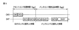
なお、書き込みパフォーマンスは、フロントエンド側の処理時間によっても変動する。そして、フロントエンド処理時間は、SDTMメモリカードを例に取れば、SDクロック周波数(SD clock frequency)に依存する。以下、このことについて説明する。図5は、マルチブロック書き込みコマンドを用いたときの書き込み動作タイミングの一例を示している。書き込み動作の第1段階では、バックエンド側は、フロントエンド側から書き込みデータが到着するまで待つ。第2段階ではバックエンド側、フロントエンド側とも動作する。したがって、マルチブロック書き込み時の書き込み時間は、フロントエンド、バックエンドに分けて考察する必要がある。なお、第2段階では、バックエンド側の書き込み時間がフロントエンド側のそれよりも主要となる。 Note that the write performance varies depending on the processing time on the front end side. The front-end processing time depends on the SD clock frequency, taking an SD ™ memory card as an example. This will be described below. FIG. 5 shows an example of the write operation timing when the multi-block write command is used. In the first stage of the write operation, the back end side waits until write data arrives from the front end side. In the second stage, both the back end side and the front end side operate. Therefore, it is necessary to consider the writing time for multi-block writing separately for the front end and the back end. In the second stage, the write time on the back end side is more dominant than that on the front end side.
バックエンド書き込み時間tWBはフラッシュメモリ(記憶領域21)への書き込みが開始されてから、全ての書き込みが完了するまでの時間の合計になる。 The back-end write time t WB is the total time from the start of writing to the flash memory (storage area 21) to the completion of all writing.
他方のフロントエンド処理時間tWFは、マルチブロック書き込みコマンドの開始からフラッシュメモリの書き込み開始までの合計時間になる。また、上記のように、SDTMメモリカードを例に取れば、フロントエンド処理時間tWFはSDクロック周波数に依存する。したがって、フロントエンド処理時間tWFは、係数CSDとSDクロック周期fSDによって表記できる。このため、SDTMメモリカードでは、tWFを[数式2]のように表記できる。 The other front-end processing time t WF is the total time from the start of the multi-block write command to the start of writing to the flash memory. Further, as described above, when an SD ™ memory card is taken as an example, the front-end processing time t WF depends on the SD clock frequency. Therefore, the front end processing time t WF can be expressed by the coefficient C SD and the SD clock period f SD . For this reason, in the SD ™ memory card, t WF can be expressed as [Equation 2].
[数式2]
フロントエンド処理時間:tWF=CSD/fSD
また、1つのAU31に記録する場合を考えると、フロントエンド処理時間tWFは書き込みコマンドの数に比例する。書き込みコマンドの数は、上述したRU32の数NRUと等価である。NRUが多くなると、すなわちRU寸法SRUが小さくなると、書き込み効率は低下する。
[Formula 2]
Front-end processing time: t WF = C SD / f SD
Further, considering the case of recording in one
移動パフォーマンスPmは、最低移動パフォーマンスの平均の最低値として定義される。これは連続したRU32を移動操作して1つの完全なAU31とするときの最低値として計算できる。移動操作の時間はバックエンド側で定義され、SDクロック周波数には左右されない。もしもメモリカード19が必ずしもRU32を移動する必要がないときには、移動パフォーマンスPmは無限大と考えてよい。これは「1/Pm=0」を意味する。
The movement performance Pm is defined as the average minimum value of the minimum movement performance. This can be calculated as the minimum value when moving
また、移動パフォーマンスPmはフラッシュメモリのプログラム時間に加え、後述の読み出し時間、およびデータ移動方法にも依存して変化する。なお、データ移動は、メモリカード19内部で処理されるものであるため、ホスト機器20が直接制御するものではない。
Further, the movement performance Pm varies depending on the read time described later and the data movement method in addition to the program time of the flash memory. The data movement is processed inside the
読み出し性能については、次の2つが定義される。 The following two are defined for the read performance.
1) データに対する読み出しパフォーマンス
データに対する読み出しパフォーマンス(読み出しパフォーマンスと称してもよい)Prは、RU32単位の読み出しをランダムに行った場合の読み出しパフォーマンスの平均値の最低値として定義される。平均は、RU32単位の読み出しを256回ランダムに行うことで計算することができる。また、各ブロック33に対するECC(Error Correcting Code)訂正に要する時間は最悪ケースを考慮しておくべきである。読み出しパフォーマンスPrは書き込みパフォーマンスPwよりも大きいか、少なくとも同等である必要がある。
1) Read performance for data Read performance for data (may be referred to as read performance) Pr is defined as the lowest value of the average value of read performance when reading is performed in units of
2) ファイルシステム(FAT)読み出し時間
FAT(ファイルアロケーションテーブル)等のファイルシステムの読み出し時間TFR(4kB)は、4kBのFATを読む最大時間として定義される。これは、書き込みの間にFAT読み出しが可能であるという条件を満足していることが必要である。リアルタイム記録の場合を考慮すれば、ホスト機器20は、RU書き込みの相互間にFAT読み出しを行うしかないからである。また、各ブロック33に対するECC訂正時間は最悪ケースを考慮しておくべきである。ファイルシステム寸法(FR寸法)SFRに対するFAT読み出し時間はシール関数(CEIL関数)を用いて、以下のように記載できる。
2) File system (FAT) read time The read time T FR (4 kB) of a file system such as FAT (file allocation table) is defined as the maximum time for reading a 4 kB FAT. This requires satisfying the condition that FAT reading is possible during writing. This is because in consideration of the case of real-time recording, the
ファイルシステム寸法SFR[kB]に対するFAT読み出し時間:TFR(SFR)

図6は、[数式1]に従って求められた、メモリカード19のパフォーマンスを示す。図6は、AU31を構成するRU32の数Ntを16としたときのパフォーマンスである。
FIG. 6 shows the performance of the
図6に示すように、使用済みRU比r(横軸)ごとのパフォーマンス(縦軸)を求め、各使用済みRU比rのパフォーマンスを結ぶとパフォーマンスカーブが得られる。パフォーマンスカーブはホスト機器メーカーにとって重要な情報になる。 As shown in FIG. 6, a performance curve is obtained by obtaining the performance (vertical axis) for each used RU ratio r (horizontal axis) and connecting the performance of each used RU ratio r. Performance curves are important information for host equipment manufacturers.
パフォーマンスカーブは書き込みパフォーマンスPwと移動パフォーマンスPmで規定される。書き込みパフォーマンスPwは使用済みRU比r=0の場合、すなわちフルパフォーマンスと等価である。 The performance curve is defined by the writing performance Pw and the movement performance Pm. The write performance Pw is equivalent to the full performance when the used RU ratio r = 0.
ここで、使用済みRU比rは、AU31中のRU32の数Ntと、使用済みRU32の数Nuを用いると、
r=Nu/Nt
と記載できる。
Here, the used RU ratio r is obtained by using the number Nt of
r = Nu / Nt
Can be described.
これは、
Nu=r×Nt
とも記載できる。
this is,
Nu = r × Nt
Can also be described.
使用済みRU比rは0から1の範囲で可変である。r=0はすべてのRU32が未使用であることを意味し、r=1はすべてのRU32が使用済みであること、すなわちパフォーマンスが0であることを意味する。言い換えれば、P(1)=0である。
The used RU ratio r is variable in the range of 0 to 1. r = 0 means that all
このことから、いかなるパフォーマンスカーブも点(1,0)を通ることがわかる。[数式1]をrを使って書き直すと、[数式3]となる。 This shows that any performance curve passes through the point (1, 0). When [Formula 1] is rewritten using r, [Formula 3] is obtained.
[数式3]
平均パフォーマンスカーブ:P(r)
=[(1−r)×Pw×Pm]/[r×Pw+(1−r)×Pm]
ただし、0≦r≦1である。この式を利用してプロットされたのが図6である。
[Formula 3]
Average performance curve: P (r)
= [(1-r) * Pw * Pm] / [r * Pw + (1-r) * Pm]
However, 0 ≦ r ≦ 1. FIG. 6 is plotted using this equation.
[2−1−3]記憶エリアの位置とパフォーマンス精度
データを書き込むRU32の開始アドレスが記憶領域21のブロック33の境界でない場合、書き込み開始位置がブロック33の境界と一致するように書き込み済みのデータを移動する時間が必要である。このため、このような場合、実際のパフォーマンスは期待パフォーマンスよりも劣る。したがって、正確なパフォーマンスを測定するためには、AとBのアドレスが消去単位(ブロック33)の境界と一致していることが要件となる。アロケーションユニットを規定するのはこの理由からである。
[2-1-3] Storage Area Position and Performance Accuracy When the start address of the
[2−2]記録中のファイルシステムの更新に関するパラメータ
ファイルシステムの更新が書き込みシーケンスに挿入されることによって、書き込み時の総合的な(実際に得られる)パフォーマンスは低下する。このため、ホスト機器20が、後述のようにメモリカード19のパフォーマンスを計算する際、ファイルシステムの更新に関するパラメータを必要とする。そして、ホスト機器20は、このパラメータを用いて、ファイルシステムの更新が書き込みシーケンスに挿入されることによる、実際のパフォーマンスの低下を計算することができる。
[2-2] Parameters related to file system update during recording When the file system update is inserted into the write sequence, the overall (actually obtained) performance at the time of writing decreases. For this reason, when the
図7はリアルタイム記録中のファイルシステムの更新の典型的なシーケンスを示している。以下、ファイルシステムの典型例としてFATが用いられた場合を例に取り説明する。 FIG. 7 shows a typical sequence of file system updates during real-time recording. Hereinafter, a case where FAT is used as a typical example of a file system will be described as an example.
ファイルシステム(FAT)の更新はどのRU32に対する書き込みの間にも起こり得る。FATの更新は定期的に行われ、あるファイルシステム更新と次のファイルシステム更新の間に書き込まれるRU32の数はファイルシステム更新間隔TFUによって規定される。このファイルシステム更新の間に書き込まれるRU32の数は、Ndである。
File system (FAT) updates can occur during writes to any
FAT書き込みサイクルは3つの書き込み動作からなる。FAT1およびFAT2は1のマルチブロック書き込みコマンドを用いたFAT1およびFAT2それぞれへのFAT情報書き込みである。ファイルシステム(FAT)の書き込みは任意のバイトアドレスから開始可能であり、16kBまでの任意の長さまでの書き込みとして定義可能である。 The FAT write cycle consists of three write operations. FAT1 and FAT2 are FAT information writes to FAT1 and FAT2, respectively, using one multi-block write command. File system (FAT) writing can start from any byte address and can be defined as writing to any length up to 16 kB.
図中DIRはディレクトリエントリ(Directry Entry)であり、これは記録に先立って生成され、ディレクトリエントリの変更した部分の512Bのみ書き込まれる。ファイルシステム書き込み時間TFWは、ファイルシステム書き込みサイクルの合計時間、すなわち、上記のFAT1、FAT2、DIRの合計書き込み時間として規定される。ファイルシステム書き込み時間TFWはデバイスコントローラ22の仕様によって変わる。
In the figure, DIR is a directory entry, which is generated prior to recording, and only the changed
[2−2−1]ファイルシステム書き込み時間TFWの平均の測定条件
ファイルシステム書き込み時間TFWは、数個の測定値の平均によって得られた値として定義される。[数式4]は平均ファイルシステム書き込み時間TFW(ave.)を規定する式である。[数式4]から分かるように、平均ファイルシステム書き込み時間TFW(ave.)として、例えば、任意の8回のファイルシステム書き込みサイクルの平均値の最悪値が用いられる。
[2-2-1] File system write measurement condition file system write time T FW average time T FW is defined as a value obtained by the average of several measurements. [Formula 4] is an expression that defines the average file system write time T FW (ave.). As can be seen from [Formula 4], for example, the worst value of the average value of any eight file system write cycles is used as the average file system write time T FW (ave.).
[数式4]
平均ファイルシステム書き込み時間:(TFW(ave.))
=[max(TFW(1)+TFW(2)+・・・+TFW(7)+TFW(8))]/8
[2−2−2]最大ファイルシステム書き込み時間
後述のように、ホスト機器20は、ファイルシステムの更新の間に、ホストバッファ27によってデータを一時保存する。このため、ホストバッファ27のサイズを決める時には、最大ファイルシステム更新時間を考慮する必要がある。ホストバッファ27のサイズに対する要求に関しては、[4−5]でさらに説明する。
[Formula 4]
Average file system write time: (T FW (ave.))
= [Max (T FW (1) + T FW (2) +... + T FW (7) + T FW (8))] / 8
[2-2-2] Maximum File System Write Time As described later, the
[数式5]はファイルシステム(FAT)書き込み時間の最悪値を規定する式である。 [Formula 5] is an expression that defines the worst value of the file system (FAT) writing time.
[数式5]
ファイルシステム(FAT)書き込み時間の最悪値:(TFW(max))≦750[ms]
[2−2−3]データ書き込みとファイルシステム書き込みの独立
ファイルシステム書き込みは、リアルタイム記録中の任意のRU間あるいはAU間に挿入可能である。デバイスコントローラ22は、ファイルシステム書き込みが、データの書き込みパフォーマンスPwそのものに影響しないように制御できる必要がある。
[Formula 5]
Worst value of file system (FAT) writing time: (T FW (max)) ≦ 750 [ms]
[2-2-3] Independent of data writing and file system writing File system writing can be inserted between any RUs or AUs during real-time recording. The
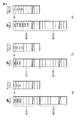
書き込みパフォーマンスPwへのファイルシステム書き込みの影響を排除するには、例えば、ファイルシステムの書き込みにより中断されたデータ書き込みの再開時の書き込みを、中断前の最後に書き込まれた物理領域の続きの領域に行うことにより実現できる。 In order to eliminate the influence of the file system write on the write performance Pw, for example, the write at the restart of the data write interrupted by the file system write is changed to the area following the physical area written last before the interruption. It can be realized by doing.
これを実現するために、例えば、ファイルシステム書き込み用のキャッシュブロックを設け、デバイスコントローラ22が、以下に示す制御を行うことができる。図8(a)に示すように、記憶領域21は、通常物理ブロック領域とキャッシュブロックとを含んでいる。図8(a)に示すように、通常物理ブロックに連続的なデータをシーケンシャルに書き込んでいる最中に、ファイルシステムの書き込み要求が来た場合、図8(b)に示すように、ファイル管理情報は、キャッシュブロックの空き領域(ページ34)に順次書き込まれる。この後、図8(c)に示すように、中断前の最後に書き込まれた領域の続きの領域(ページ34)からデータの書き込みを再開する。
In order to realize this, for example, a cache block for writing a file system is provided, and the
従来のようにデータ書き込み再開時の書き込み位置を再開前の最後に書き込まれた物理領域の続きではない物理領域(例えば、新たなブロック(BLOCK2等)内の領域)とすると、引越し書き込みが発生し、書き込みパフォーマンスPwそのものがファイルシステム書き込みにより変動する。 If the writing position when resuming data writing is a physical area that is not a continuation of the last written physical area (for example, an area in a new block (such as BLOCK2)) as in the prior art, moving writing occurs. The write performance Pw itself varies depending on the file system write.
なお、通常のデータとファイル管理情報との選別は、例えば、アドレス、サイズ、シーケンスを調べることによって実現できる。 Note that selection between normal data and file management information can be realized, for example, by examining addresses, sizes, and sequences.
[3]メモリカードの分類
メモリカード19のパフォーマンスとホスト機器20が要求する性能との整合を取ることを容易にするために、メモリカード19は、カードパフォーマンスに応じて複数のクラス(性能クラス)に分類される。各クラスは、例えば、上記のパフォーマンスカーブおよびファイルシステム書き込み時間TFW等の性能パラメータに応じて分類される。そして、クラスの情報は、メモリカード19の性能識別コード24として、デバイスコントローラにおいて保持される。
[3] Classification of Memory Cards In order to facilitate matching between the performance of the
メモリカード19は、目視によって認識可能な方法で、自身のクラスを表示する。図9は、クラス表示を示すラベルを例示している。この図は、記憶デバイス19が、SDTMメモリカードである場合を例示している。
The
例えば、図9に示すように、メモリカード19は、記憶領域21、デバイスコントローラ22の少なくとも一部を覆う外囲部71を有し、外囲部71上にクラスを表示するラベル72を有する。
For example, as shown in FIG. 9, the
また、ホスト機器20にも、クラスが設定されている。この場合、同じクラスのメモリカード19を用いると最大性能が出せることを意味する。下位クラスのメモリカード19を用いた場合でも最大性能は出せないが記録は可能である。ホストのクラス表示は必須ではないが、図9では、ホスト機器20の外囲部73に、クラスを表示するラベル74が設けられる例を示す。
A class is also set in the
[3−1]アプリケーションからの要求
ホスト機器20のアプリケーションは、アプリケーションが用いるメモリカード19に高性能のパフォーマンスを求めている。以下に代表例を記す。
[3-1] Request from Application The application of the
(1)デジタルビデオ録画
MPEG2やMotionJPEGではメモリカード19への直接記録が求められている。標準的なテレビ画像の品質、解像度を得るには、約2MB/secカード性能が求められる。また、高品質の画像記録には、約4MB/secのカード性能が求められる。
(1) Digital video recording In MPEG2 and Motion JPEG, direct recording to the
(2)連写機能を有するデジタルスチルカメラ
デジタルスチルカメラメーカーは連写機能を実現するために高性能のメモリカード19を必要としている。デジタルスチルカメラメーカーは使用者に可能な連写レートを明示する場合は、カードパフォーマンスとホスト機器20の制御方法から計算することができる。
(2) Digital Still Camera Having Continuous Shooting Function Digital still camera manufacturers need a high-
[3−2]クラス分け
図10は、パフォーマンスカーブとクラスとの関係を示している。図10は、2本のパフォーマンスカーブで区分した場合の3つの領域を示す。図10に示すように、クラス2およびクラス4のパフォーマンスカーブで、縦軸P(r)と横軸rからなる領域は3領域に区分されている。なお。縦軸P(r)はパフォーマンスを、横軸rは使用済みRU比を示している。
[3-2] Classification FIG. 10 shows the relationship between the performance curve and the class. FIG. 10 shows three regions when divided by two performance curves. As shown in FIG. 10, in the performance curves of
従来のカードは、この3領域のうち、もっとも原点に近い領域、クラス0(図中Class 0)に属する。図中では最も性能の劣った区分である。
The conventional card belongs to the class 0 (
クラス1のパフォーマンスカーブはクラス2カードの最低性能を意味する。このカーブは2つのパラメータPw1(クラス2パフォーマンスカーブとY軸の交点)とPm1で規定される。
A
同様に、クラス4のパフォーマンスカーブはクラス4カードの最低性能を意味する。このカーブは2つのパラメータPw2(クラス4パフォーマンスカーブとY軸の交点)とPm2で規定される。
Similarly, a
アプリケーションの要求がさらに高まればさらに高レベルのクラス8、クラス10のパフォーマンスカーブを規定する必要が出てくるが、基本的な考え方は変更する必要はない。クラス8のパフォーマンスカーブが定義された場合、このクラス8のパフォーマンスカーブよりも性能が低く、クラス6のパフォーマンスカーブ以上の性能の領域がクラス6の領域となり、クラス8のパフォーマンスカーブ以上の性能の領域がクラス8の領域となる。
If the application requirements are further increased, it will be necessary to define higher-
図11は、各クラスに要求される特性の例を示している。クラス2(CLASS2)カード、クラス4(CLASS4)、クラス6(CLASS6)、カードで必要とされるパフォーマンスパラメータの例は、下記および図11のようになっている。 FIG. 11 shows an example of characteristics required for each class. Examples of performance parameters required for a class 2 (CLASS2) card, class 4 (CLASS4), class 6 (CLASS6), and card are as shown below and FIG.
CLASS2:Pw=2[MB/sec]、Pm=1[MB/sec]、Pr=2[MB/sec]
CLASS4:Pw=4[MB/sec]、Pm=2[MB/sec]、Pr=4[MB/sec]
CLASS6:Pw=6[MB/sec]、Pm=3[MB/sec]、Pr=6[MB/sec]
また、平均ファイルシステム書き込み時間TFW(ave.)、最大ファイルシステム書き込み時間TFW(max)、ファイルシステム読み出し時間TFR(4kB)は、各クラスとも同じで、それぞれ、例えば100[ms]、750[ms]、4[ms]である。
CLASS2: Pw = 2 [MB / sec], Pm = 1 [MB / sec], Pr = 2 [MB / sec]
CLASS4: Pw = 4 [MB / sec], Pm = 2 [MB / sec], Pr = 4 [MB / sec]
CLASS6: Pw = 6 [MB / sec], Pm = 3 [MB / sec], Pr = 6 [MB / sec]
The average file system write time T FW (ave.), The maximum file system write time T FW (max), and the file system read time T FR (4 kB) are the same for each class, for example, 100 [ms], 750 [ms] and 4 [ms].
図11の例によれば、クラス2のカードのパフォーマンスカーブは、Y軸と2[MB/sec]の点で交わり、X軸と1の点で交わり、途中で原点側によった曲線になる。その曲線以上の性能の領域で、後述のクラス4カードのパフォーマンスカーブまでの第1象限領域がクラス2カードの領域になる。
According to the example of FIG. 11, the performance curve of the
同様にクラス4カードのパフォーマンスカーブはY軸と4[MB/sec]の点で交わり、X軸と1の点で交わり、クラス2カードのパフォーマンスカーブよりもさらに原点から離れた領域に存在する。このクラス4カードのパフォーマンスカーブの原点と逆の側の領域がクラス4カードの領域になる。
Similarly, the performance curve of the
同様に、Y軸と6[MB/sec]の点で交わる、クラス6のパフォーマンスカーブが定義できる。
Similarly, a
図11に例示した各クラスのカード要求特性の測定条件の例を図12に示す。上記のように、書き込みパフォーマンスPwは、フロントエンド処理時間tWFおよびRU寸法SRUによって影響され、フロントエンド処理時間tWFは、SDクロック周波数fSDによって影響される。そして、SDクロック周波数fSDとRU寸法SRUを図12に示す値に設定して、各クラスの要求特性を測定条件している。なお、パフォーマンスをより高くするためには、ホストは大きなRU寸法でアクセスすることが望ましい。 FIG. 12 shows an example of measurement conditions for the card requirement characteristics of each class illustrated in FIG. As described above, the write performance Pw is affected by the front end processing time t WF and the RU dimension S RU , and the front end processing time t WF is affected by the SD clock frequency f SD . The SD clock frequency f SD and the RU dimension S RU are set to the values shown in FIG. 12, and the required characteristics of each class are measured. In order to improve performance, it is desirable for the host to access with a large RU size.
[3−3]容量とAU最大寸法との関係
ブロックサイズに関係してホスト機器20から別のパラメータが要求される。メモリカード19の物理規格によりAU寸法SAUを送出するレジスタを規定することによって、ホスト機器20に対して、メモリカード19にとって最適なAU寸法SAUを明示することができる。この結果、ホスト機器20は、AU31を効率的に利用できる。なお、後述のように、AU31の最大値によって、ホストバッファ27の必要なサイズが規定される。
[3-3] Relationship between Capacity and AU Maximum Size Another parameter is requested from the
メモリカード19の容量に応じた最大AU寸法の例をあげる。
An example of the maximum AU dimension corresponding to the capacity of the
カード容量/最大AU寸法=16乃至128MB/128kB、256MB/256kB、512MB/512kB、1GB/1MB、2GB/2MB、4乃至32GB/4MB
[3−4]読み出しパフォーマンス要求
クラス2、クラス4、クラス6のカードはRU32単位の読み出しを行った場合、それぞれ最低2[MB/sec]、4[MB/sec]、6[MB/sec]の読み出し性能が規定されている。ただし、これはホスト機器からの読み出し能力を保証するものではない。上記にはホスト機器の環境を考慮していないからである。
Card capacity / maximum AU size = 16 to 128MB / 128kB, 256MB / 256kB, 512MB / 512kB, 1GB / 1MB, 2GB / 2MB, 4 to 32GB / 4MB
[3-4] Read Performance Request When the
[3−5]カードの物理規格を規定する要件
以上述べたクラスおよび各種のパラメータにより規定されるパフォーマンスを規格化する際、このパフォーマンス規格が、現行規格と将来規格を包含する必要がある。これらの規格に加えて将来のメモリカードも包含できる必要がある。このため、たとえば現在のSDTMメモリカードでは、書き込みパフォーマンスPw、移動パフォーマンスPm、フィルシステム書き込み時間TFW等のパラメータは物理規格1.01、1.10に合うように規定される必要がある。
[3-5] Requirements for Defining Physical Standards of Cards When standardizing the performance defined by the classes and various parameters described above, this performance standard needs to include the current standard and the future standard. In addition to these standards, future memory cards need to be included. For this reason, for example, in the current SD ™ memory card, parameters such as the write performance Pw, the movement performance Pm, and the fill system write time T FW need to be defined so as to meet the physical standards 1.01 and 1.10.
あるクラス(例えば、将来定義されるであろう高クラス)のメモリカード19は、このクラスを定義するのに必要な条件(例えば、SDクロック周波数等)の制約から、ある物理規格(例えば、物理規格1.01)に則って製造することができない。このようなクラスのメモリカード19は、より高度の物理規格に則って製造される必要がある。例えば、クラス6カードは、ハイスピードモード(High Speed Mode)を必要とするため、物理規格1.01では製造することができない。物理規格1.10以上である必要がある。
A
[3−6]クラスおよび各種パラメータ等のデータの保持
新規規格では、例えば、クラス、AU寸法SAU、移動パフォーマンスPm、係数CSDをメモリカードのステータス情報としてレジスタに保持することができる。より具体的には、例えば、クラスは、性能識別コードレジスタ24に格納されている。AU寸法SAU、移動パフォーマンスPm、係数CSDは、性能パラメータレジスタ25に格納されている。
[3-6] Retention of data such as class and various parameters In the new standard, for example, class, AU dimension S AU , movement performance Pm, coefficient C SD can be retained in the register as status information of the memory card. More specifically, for example, the class is stored in the performance
このように、クラスおよび各種パラメータを、メモリカード19が保持することによって、クラスを識別可能なホスト機器20が、パフォーマンスをさらに正確に計算することを可能とし、さらに効率よくメモリカード19を利用できる。
As described above, the
図13に、SDTMメモリカードの場合の、レジスタ情報のビット幅の例を記載する。SDTMメモリカードの場合、AU寸法SAU、移動パフォーマンスPm、係数CSD、を、例えば、レジスタ内のSDカードステータスなどに規定することができる。これらのデータは別に用意されているレジスタに記入しても良い。本性能規格をサポートしないカードでは、これらのフィールドを0に設定しておけばよい。そのようなメモリカードはクラス0カードと認識される。
FIG. 13 shows an example of the bit width of the register information in the case of the SD ™ memory card. In the case of the SD ™ memory card, the AU dimension S AU , the movement performance Pm, and the coefficient C SD can be defined in, for example, the SD card status in the register. These data may be entered in a separately prepared register. For cards that do not support this performance standard, these fields may be set to zero. Such a memory card is recognized as a
また、クラスの情報は、従来の記憶デバイスの、例えば固定値が読み出される(例えば0)ところに定義されることができる。これにより、本実施形態に対応できていない従来デバイスを性能分類の対象外であるクラス0カードと識別することもできる。
The class information can be defined in a conventional storage device where, for example, a fixed value is read (for example, 0). Thereby, a conventional device that is not compatible with the present embodiment can be identified as a
なお、書き込みパフォーマンスPwは、各クラスに応じて決定されている(クラスが要求する書き込みパフォーマンスが決定されている)。このため、ホスト機器20は、クラスを読み取ることにより、書き込みパフォーマンスPwを知得することができる。
The write performance Pw is determined for each class (the write performance required by the class is determined). For this reason, the
性能識別コードレジスタ24および性能パラメータレジスタ25内の情報は、例えば、ホスト機器20からの所定のコマンドを受けた際に、ホスト機器20に対して出力するようにすることができる。
Information in the performance
性能識別コードレジスタ24および性能パラメータレジスタ25に設定される値は、製造時にあらかじめ計算された値を書き込むことも、メモリカード19自体が初期化時に決定することもできる。
The values set in the performance
また、現在のSDTMメモリカードは、具体的な性能パラメータを示す手段(専用レジスタ)を持たないので、プログラム可能なレジスタのリザーブ領域に性能コードと性能パラメータを追加することにより、ホストは性能コードを見ればカードの性能が分かるようにできる。これにより現在のカードコントローラを変更することなく流用できる。 In addition, since the current SD ™ memory card does not have a means (dedicated register) for indicating a specific performance parameter, the performance code and the performance parameter are added to the reserved area of the programmable register so that the host Can see the performance of the card. As a result, the current card controller can be used without being changed.
[4]リアルタイム記録を行う際のホスト機器の動作シーケンスおよび要件
[4−1]リアルタイム記録を行う際のホスト機器の動作シーケンス
リアルタイム記録を行う際のホスト機器20は、上記のパフォーマンスカーブ、クラス、各種パラメータを用いて以下に述べるシーケンスによって計算を行いながら、書き込みを行うことができる。そして、ホスト機器20は、リアルタイム記録の際に、以下に述べるシーケンスを取ることが望ましい。
[4] Operation sequence and requirements of host device when performing real-time recording [4-1] Operation sequence of host device when performing real-time recording The
(1)ホスト機器20に搭載されているアプリケーションから要求されるパフォーマンス(以下、アプリケーションパフォーマンス)Paを決定する。
(1) A performance (hereinafter referred to as application performance) Pa requested from an application installed in the
(2)適当な、ファイルシステム更新間の書き込みRU数Ndを選ぶ。 (2) Select an appropriate number Nd of write RUs between file system updates.
(3)ファイルシステム更新を考慮して、アプリケーションパフォーマンスPaを実現するために必要なカードパフォーマンスPcを決定する。 (3) The card performance Pc necessary for realizing the application performance Pa is determined in consideration of the file system update.
(4)最大使用済みRU比r(Pc)を決定する。 (4) The maximum used RU ratio r (Pc) is determined.
(5)各AU31をAUfastとAUslowに区分する。
(5) Each
(6)記録可能時間Trecを推定する。 (6) The recordable time T rec is estimated.
(7)ファイルシステム更新間の書き込みRU数Ndを調整する。ファイルシステム更新間の書き込みRU数Ndが大きければパフォーマンスは改善される。 (7) Adjust the number of write RUs Nd between file system updates. If the number Nd of write RUs between file system updates is large, the performance is improved.
(8)計算の結果、充分なパフォーマンス、充分な記録可能時間が得られなければ、カードの消去が必要になる。 (8) If sufficient performance and sufficient recordable time are not obtained as a result of the calculation, the card needs to be erased.
以下、動作(1)乃至(8)を行うための具体的な方法およびホスト機器20の要件について説明する。
Hereinafter, a specific method for performing the operations (1) to (8) and requirements of the
[4−2]ファイルシステム更新に伴うパフォーマンス計算方法
リアルタイム記録時の典型的なファイルシステム(FAT)更新サイクルのシーケンスは、図7に示した通りである。ホスト機器20は、ファイルシステム更新時に、このシーケンスを取ることが望ましい。
[4-2] Performance Calculation Method Associated with File System Update A typical file system (FAT) update cycle sequence during real-time recording is as shown in FIG. The
[4−2−1]ファイルシステム更新を考慮したカードパフォーマンス条件
ホスト機器20は、Paを満足するために必要なカードパフォーマンスPcを、アプリケーションパフォーマンスPa、および平均ファイルシステム書き込み時間TFWから決定する。上記のように、ファイルシステム書き込みシーケンスが挿入されることにより、書き込み時の総合的なパフォーマンスは低下する。よって、ホスト機器20は、一般に、アプリケーションパフォーマンスPaよりも高いカードパフォーマンスPcを有するカードを必要とする。
[4-2-1] Card Performance Condition Considering File System Update The
また、ホスト機器20によっては、アプリケーションの種類に応じて数種類の異なったビットレートのモードに対応していることがある。ホスト機器20は、この場合、利用者が選んだモードに応じて、アプリケーションパフォーマンスPaを決める。
Depending on the type of application, some
なお、ホスト機器20は、アプリケーションパフォーマンスPaに合わないメモリカード19を拒絶するのではなく、メモリカード19のクラスに合わせて、ホスト機器20のパフォーマンスを整合するようにすることが望ましい。
It is desirable that the
例えば、あるメモリカード19のカードパフォーマンスがアプリケーションパフォーマンスPaに対して不足しているときは、ホスト機器20は、より小さなアプリケーションパフォーマンスPaを要求するモードに切り替えることが望ましい。例えば、データの圧縮率を上げたり、画像の解像度を下げたり、フレームレートを下げたりすることにより、ホスト機器20は、より低いアプリケーションパフォーマンスPaに適合することができる。この手法を実現できるように、ホスト機器20はパフォーマンスの低いメモリカード19を利用可能とするために数種類の書き込みモードを持つことが望ましい。
For example, when the card performance of a
また、ホスト機器20が、異なる記録性能を持つ複数のモードを持つことにより、異常事態が発生した場合でもより低速なモードにすることで記録を可能にすることができる。これは、例えば、クラス0カードの場合、ホスト機器20は、カード性能がわからないため、実際にあるモードで試してみなければ、そのモードが動作するかわからないためである。
In addition, since the
アプリケーションパフォーマンスPa、Paを満足するために必要なカードパフォーマンス(以下、カードパフォーマンス)Pcを[数式6]、[数式7]にそれぞれ示す。 Card performance (hereinafter referred to as card performance) Pc necessary to satisfy the application performances Pa and Pa is shown in [Formula 6] and [Formula 7], respectively.
[数式6]
アプリケーションが要求するパフォーマンス:Pa
=(Sc×Nd)/(Sc×Nd/Pc+TFW)
[数式7]
Paを満足するために必要なカードパフォーマンス:Pc
=(Sc×Nd×Pa)/(Sc×Nd−Pa×TFW)
カードパフォーマンスPcは、ファイルシステム更新間の書き込みRU数Ndによって変化し、図7からも分かるように、ファイルシステム更新間の書き込みRU数Ndは、ファイルシステム更新の頻度によって変化する。よって、カードパフォーマンスPcは、ファイルシステムの更新の頻度によって影響される。ファイルシステムの更新の頻度の決定の仕方は、次の[4−2−2]で述べる。
[Formula 6]
Performance required by application: Pa
= (Sc × Nd) / (Sc × Nd / Pc + T FW )
[Formula 7]
Card performance required to satisfy Pa: Pc
= (Sc × Nd × Pa) / (Sc × Nd−Pa × T FW )
The card performance Pc varies depending on the number of write RUs Nd between file system updates. As can be seen from FIG. 7, the number of write RUs Nd between file system updates varies depending on the frequency of file system updates. Therefore, the card performance Pc is affected by the frequency of updating the file system. The method of determining the frequency of updating the file system will be described in [4-2-2] below.
[4−2−2]ファイルシステム更新期間の条件
ファイルシステム(FAT)更新期間(ファイルシステム更新から次のファイルシステム更新までの期間)は、ファイルシステム書き込みシーケンスを各データ転送の間に挿入することにより決定される。したがって、ファイルシステム更新期間は、書き込み速度に依存するが、期間の精度は重要ではない。ホスト機器20がファイルシステム更新期間を簡単に計算できるように、簡単な方法をとってよい。
[4-2-2] Conditions for file system update period In the file system (FAT) update period (period from the file system update to the next file system update), a file system write sequence is inserted between each data transfer. Determined by. Therefore, the file system update period depends on the writing speed, but the accuracy of the period is not important. A simple method may be adopted so that the
ファイルシステム更新期間の算出式を[数式8]に示す。 A formula for calculating the file system update period is shown in [Formula 8].
[数式8]
ファイルシステム更新期間:TPF
=Sc×Nd/Pa
=Sc×Nd/Pc+TFW(ave.)
ホスト機器20は、ファイルシステム書き込みによるカードパフォーマンスの低下の程度を考慮して、ファイルシステム更新の間に書き込まれるRU数Ndを適切な値に調整してよい。ただし、ファイルシステム更新期間TPFは1秒以上が望ましい。
[Formula 8]
File system update period: T PF
= Sc x Nd / Pa
= Sc × Nd / Pc + T FW (ave.)
The
より大きなRU数Ndが選択されたとき、カードパフォーマンスPcはアプリケーションパフォーマンスPaに近づく。こうすることにより、低性能のメモリカード19でもアプリケーションパフォーマンスPaを満足しうるようになり得る。
When a larger RU number Nd is selected, the card performance Pc approaches the application performance Pa. As a result, the low
ファイルシステム更新期間の決め方の別の方法として、ファイルシステム更新間隔TFU(TPFと等価なもの)をホスト機器20のタイマーを用いて決めることができる。この場合、TFUは一定である。ファイルシステム更新はRU書き込みの間に挿入される。このため、ファイルシステム更新間の書き込みRU数Ndは、ファイルシステム更新間隔TFUによって変動する。
As another method of determining the file system update period, the file system update interval T FU (equivalent to T PF ) can be determined using the timer of the
この場合、ファイルシステム更新間隔TFUの間のデータ量は、[数式9]のようになる。 In this case, the amount of data during the file system update interval TFU is represented by [Formula 9].
[数式9]
TFUの間のデータ量:Pa×TFU
=Pc×(TFU−TFW(ave.))
[数式9]を変形することにより、カードパフォーマンスPcが、[数式10]のように表現される。
[Formula 9]
Data volume during TFU : Pa x TFU
= Pc × (T FU −T FW (ave.))
By modifying [Formula 9], the card performance Pc is expressed as [Formula 10].
[数式10]
Paを満足するためのカードパフォーマンス:Pc
=(Pa×TFU)/(TFU−TFW(ave.))
[4−3]アロケーションユニット(AU)の分類
ホスト機器20は、どのAU31がリアルタイム記録に使用可能かを判定する。すなわち、各AU31が、求められたカードパフォーマンスPcを満たすかを判定する。各AU31のパフォーマンスは、図6から分かるように、使用済みRU比rによって変化するので、各AU31が、使用済みRU比rを閾値として用いて判定される。
[Formula 10]
Card performance to satisfy Pa: Pc
= (Pa × T FU ) / (T FU −T FW (ave.))
[4-3] Classification of allocation unit (AU) The
[4−3−1]最大使用済みRU比
図4に示したように、書き込み開始位置Aおよび終了位置BがそれぞれAU31の境界と一致しているとすれば、[数式3]によりAU31のパフォーマンスの計算を求めることができる。
[4-3-1] Maximum Used RU Ratio As shown in FIG. 4, assuming that the write start position A and the end position B coincide with the boundary of the
そして、カードパフォーマンスPcから、最大使用済みRU比r(Pc)が導ける。すなわち、最大使用済みRU比r(Pc)は、[数式3]の逆関数として求められる。 The maximum used RU ratio r (Pc) can be derived from the card performance Pc. That is, the maximum used RU ratio r (Pc) is obtained as an inverse function of [Formula 3].
最大使用済みRU比r(Pc)以下の使用済みRU比rを有するAU31は、カードパフォーマンスPcを満たすAUである。そして、使用済みRU比rが小さいほどリアルタイム記録に適したAUであり、最大使用済みRU比r(Pc)を境界として、後述のように、AU31がAUfastとAUslowに分類される。
An
[数式11]に最大使用済みRU比r(Pc)の計算式を示す。 [Formula 11] shows a formula for calculating the maximum used RU ratio r (Pc).
[数式11]
最大使用済みRU比:r(Pc)
=[(Pw−Pc)×Pm]/[(Pw−Pm)×Pc+Pw×Pm]
[4−3−2]2つのカテゴリへのAUの分類
ホスト機器20は、AU31を2つのカテゴリに分類する。ひとつはAUfast(適合管理単位領域)であり、これはカードパフォーマンスPcでリアルタイム記録を行うのに充分対応できる速さを有する。他方はAUslow(不適管理単位領域)であり、これはメモリ領域が断片化し過ぎているためにリアルタイム記録に適さないものである。
[Formula 11]
Maximum used RU ratio: r (Pc)
= [(Pw−Pc) × Pm] / [(Pw−Pm) × Pc + Pw × Pm]
[4-3-2] Classification of AU into two categories The
ホスト機器20は、AU31ごとに使用済みRU数Nuを数え、使用済みRU数Nuから使用済みRU比rを計算する。AUfastかAUslowかは[数式12]により判定できる。
The
[数式12]
Nu/Nt<r(Pc)であればAUはAUfast
Nu/Nt≧r(Pc)であればAUはAUslow
すなわち、(使用済みRU数Nu)/(AU中の全RU数Nt)が最大使用済みRU比r(Pc)未満のときはAUはAUfastに分類され、最大使用済みRU比r(Pc)以上のときはAUslowに分類される。
[Formula 12]
If Nu / Nt <r (Pc), AU is AU fast
If Nu / Nt ≧ r (Pc), AU is AU slow
That is, when (used Ru number Nu) / (total RU number Nt in AU) is less than the maximum used RU ratio r (Pc), the AU is classified as AU fast , and the maximum used RU ratio r (Pc) In the above case, it is classified as AU slow .
図14は、記憶領域21におけるAU31の割り当てを示しており、上記で説明したAU31の2種類の記憶領域21内での分布の一例を示している。先頭のAU31は、ファイルシステムを含むため、リアルタイム記録には適さない領域であり、AUslowに割り当てられる。また、ディレクトリエントリはデータを記録するAU31と同じAU31に作成してはならない。
FIG. 14 shows allocation of
AU1およびAU4は、ファイルシステムを含むものではないが、(使用済みRU数Nu)/(AU中の全RU数Nt)が最大使用済みRU比r(Pc)以上となっているため断片化していると判断され、AUslowと分類されている。 Although AU1 and AU4 do not include a file system, they are fragmented because (used Ru number Nu) / (total RU number Nt in AU) is equal to or greater than the maximum used RU ratio r (Pc). Is classified as AU slow .
[4−4]記録可能時間
ホスト機器20は、リアルタイム記録が可能な時間を[数式13]により計算できる。[数式13]において、Nrは、AUfastと判定された全てのAU31内の書き込み可能なRU32の数Nrである。充分な記録可能時間が準備できないときは、ホスト機器20は、例えばユーザに記録したデータを別のところに移動するように指示するか、メモリカード19を再フォーマットするように指示する必要がある。
[4-4] Recordable Time The
[数式13]
記録可能時間:TREC
=Sc×Nr/Pa
または、ホスト機器20は、ファイルシステム更新間の書き込みRU数Ndを大きくした場合、すなわち、ファイルシステム更新期間TPFを大きくした場合、記録時間を再度計算する。ファイルシステム更新間の書き込みRU数Ndを大きくすることにより、パフォーマンスが改善されるからである。すなわち、最大使用済みRU比r(Pc)の値が大きくなり、AUfastの数が増えるため、記録時間が増加する。
[Formula 13]
Recordable time: T REC
= Sc x Nr / Pa
Alternatively, when the
[4−5]ホスト機器のバッファに必要とされる要件
ホストバッファ27は、データを一時的に保存するために十分な大きさを有する必要がある。ホストバッファ27には下記の要件が求められる。
[4-5] Requirements Necessary for Buffer of Host Device The
[4−5−1]ホスト機器バッファの寸法要件
ホストバッファ27は、以下に示す要求を満たす大きさを有している必要がある。
[4-5-1] Dimensional Requirements for Host Device Buffer The
(1)ファイルシステム(FAT)更新に応じた要求
ホスト機器20がファイルシステムを更新するとき、ホストバッファ27は、ファイルシステム書き込み中に本来書き込むべきデータを一時的に保存するために用いられる。このため、大きなバッファの大きさが必要とされる。上記のファイルシステム書き込み時間の最悪値TFW(max)として規定される。ファイルシステム書き込み時間の最悪値TFW(max)は、例えば、[数式5]に示すように、750[ms]である。なお、バッファの大きさは、一般的に、一定時間の記録データを保存可能な領域として記録時間に換算して記述される。
(1) Request according to file system (FAT) update When the
(2)誤り(エラー)訂正に応じた要求
ホストバッファ27は、書き込みデータの誤りを訂正しているときの遅延を補完するときにも用いられる。書き込みの誤りが発生したとき、メモリカード19はCRCステータスを返さないか、エラーを表示してマルチブロック書き込みを停止する。ホストバッファ27は、誤りが発生した場合に再書き込みを行うことができるように、書き込みが完了するまでデータを保持する必要がある。
(2) Request according to error (error) correction The
エラーが発生してもホスト機器20がリアルタイム記録を継続できるようにするため、ホストバッファ27は、例えば、250[ms]分の大きさを有することが必要である。これは、メモリカード19の書き込み完了時間の最大値として250[ms]が規定されていることに対応している。したがって、上記のファイルシステム書き込み時間の最悪値TFW(max)に要する時間と合わせた大きさが必要である。ファイルシステム書き込み時間の最悪値TFW(max)が例えば750[ms]の場合、合わせて1[s]分のデータを貯めるバッファが必要である。
In order to allow the
(3)AUの書き込み遅延補償に応じた要求
使用済みRU32がAU31の上部に集まったときも含めてAU31内に書き込み済みのRU32がある場合、使用済みRU32に格納されているデータが他のRU32へ移動されない限り、書き込みデータを書き込むことができない。したがって、書き込み済みRU32を移動している間、書き込みデータはホストバッファ27に保管されなければならない。
(3) Request according to AU write delay compensation When there is a written
図15にホストバッファ27の概念を示す。図15に示すように、ホスト機器20からホストバッファ27に一定のレートPaで連続的にデータが入力されていると仮定する。また、ホスト機器20はホストバッファ27に蓄積されたデータを読んでそれをAU31に書き込むものとする。
FIG. 15 shows the concept of the
一方、ホストバッファ27から出力されるデータのレートは、AU31の断片化の状態に依存する。すなわち、上記のように、AU31内に書き込み済みのRU32がある場合、書き込みデータは、ホストバッファ27において保持され、出力されない。そして、AU31内に書き込み済みRU32が無い場合、またはRU32の移動が終了すると、ホストバッファ27は、データをレートPwで出力する。
On the other hand, the rate of data output from the
以上より、ホストバッファ27の必要な寸法はAU31中の全使用済みRU32の移動が行われる時間から求められる。
From the above, the necessary size of the
なお、ホストバッファ27のサイズが十分でなくなったときは、AUfast内でのデータの断片化状態に依存してホストバッファ27のオーバーフロー(バッファの不足)が起こることがある。このため、ホストバッファ27のサイズと、AUfastの断片化状態とに応じてさらに更なる検討が必要になる場合がある。
Note that when the size of the
(4)書き込みデータの準備
ホスト機器20が書き込みデータを準備するにはある程度の時間がかかり、書き込みデータの生成は離散的になってしまう。このデータを一旦ホストバッファ27を介して、ホストコントローラ26からデータを書き込むようにすることができる。こうすることにより、空き時間なく転送ができるため、効率の良い転送が可能になる。
(4) Preparation of write data It takes a certain amount of time for the
特に、リアルタイム記録の場合、リアルタイムデータをFIFOとしてのホストバッファ27に一旦蓄積してからメモリカード19に書き込みを行うことにより、リアルタイムデータの準備(計算)時間を見えなくすることができる。すなわち、効率良くメモリカード19にデータを記録できる。
In particular, in the case of real-time recording, the real-time data preparation (calculation) time can be made invisible by temporarily storing the real-time data in the
なお、システムメモリ上で計算してデータをメモリカード19に直接書き込む場合は、処理がシーケンシャルとなる。このため、データの計算と書き込みを交互に行う必要がある。テータの計算と書き込みを交互に行うと、データ計算中はメモリカード19には何も書き込まれず無駄な時間となるため、メモリカード19が示すクラスよりも低い性能しか引き出すことができなくなってしまう。
In addition, when calculating in the system memory and writing the data directly to the
必要なバッファサイズはアプリケーションパフォーマンスPa、移動パフォーマンスPm、最大使用済みRU比r(Pc)、AU寸法SAUの関数として記述できる。 The necessary buffer size can be described as a function of application performance Pa, movement performance Pm, maximum used RU ratio r (Pc), and AU dimension S AU .
[数式14]に必要とされるバッファサイズSBUFを示す。ただし、この式の右辺の第1項(Pa)は、上記の(1)、(2)の記載内容に対応し、右辺の第2項は上記の(3)の記載内容に対応するが、上記の(4)については、[数式14]に含まれていない。また、ホスト機器20の規格によってはさらに付加的なバッファが必要になる。
[Equation 14] shows the buffer size S BUF required. However, the first term (Pa) on the right side of this equation corresponds to the description of (1) and (2) above, and the second term on the right side corresponds to the description of (3) above. The above (4) is not included in [Formula 14]. Further, depending on the standard of the
[数式14]
必要なバッファサイズ:SBUF>Pa+[r(Pc)×SAU×Pa]/Pm
もしもアプリケーションパフォーマンスPaが移動パフォーマンスPmよりも小さく、ホストバッファ27が、Pa+SAUを上回る充分な大きさを有しているとき、[数式14]は常に満足される。
[Formula 14]
Required buffer size: S BUF > Pa + [r (Pc) × S AU × Pa] / Pm
If the application performance Pa is smaller than the movement performance Pm and the
[4−5−2]ホストバッファサイズが小さい場合の取り扱い
以下は、上述の議論とは独立して、ホストバッファ27の大きさが不十分な場合に、断片化度合いが小さいAUfastを見つける方法について述べる。ただし、ここに述べる方法を取るよりも、ホストバッファ27が十分な大きさを持つことが好ましい。
[4-5-2] Handling when the host buffer size is small The following is a method of finding an AU fast with a small degree of fragmentation when the size of the
図16は、全ての使用済みRU32がAU31の上部に集積している場合を示している。最大使用済みRU比r(Pc)は使用済みRU32cと未使用RU32dで分けられる場所を示している。ホスト機器20が、最初の未使用RU32dにデータを書き込むとき、メモリカード19は全ての使用済みRU32cの移動が完了するまで長いビジーを出す。この間、書き込みデータはホストバッファ27に蓄えられる。このとき、AU31中の全ての使用済みRU32cの移動に要する時間は、(r(Pc)×SAU)/Pmである。よって、ホストバッファ27に求められる大きさを[数式15]に示す。
FIG. 16 shows a case where all the used
[数式15]
ホストバッファサイズ:SBUF>Pa×[(r(Pc)×SAU)/Pm]
[数式15]より、[数式16]が得られる。
[Formula 15]
Host buffer size: S BUF > Pa × [(r (Pc) × S AU ) / Pm]
From [Formula 15], [Formula 16] is obtained.
[数式16]
ホストバッファサイズによって限定される使用済みRU比
=r(Pc)<[(Pm×SBUF)/(Pa×SAU)]
[数式16]から分かるように、ホストバッファ27のサイズが小さい場合、最大使用済みRU比r(Pc)が、ホストバッファ27の大きさによって制限される。そして、この場合、ホストバッファ27の大きさによって制限された最大使用済みRU比r(Pc)を[数式12]内のr(Pc)として用いてAU31を分類する必要がある。
[Formula 16]
Used RU ratio limited by the host buffer size = r (Pc) <[(Pm × S BUF ) / (Pa × S AU )]
As can be seen from [Equation 16], when the size of the
また、ホストバッファ27のサイズが小さい場合、リアルタイムデータ記録中にホストバッファ27に蓄積されたデータの大きさを観測し、その結果に応じて、データのビットレートを一時的に小さく制御するか、ファイルシステムの更新間隔を制御して事前にバッファオーバーフローを回避することができる。ホストバッファ27がオーバーフローしてデータを喪失してしまうのは問題があるため、データの品質を落としてでもデータ喪失を防ぐことが必要である。
If the size of the
また、記憶デバイス19の性能情報(性能パラメータ)に基づいて予測した書き込み性能で記録をしたとき、ホスト機器20は、バッファオーバーフローの発生や記憶デバイス19のアクセス中にエラーが頻発した際、記憶デバイス19の性能情報に基づいた速度よりも低速のモードに切り替えることができる。
When recording is performed with the write performance predicted based on the performance information (performance parameter) of the
[4−6]その他
ホスト機器20は、メモリカード19の性能情報(クラス、性能パラメータ等の情報)と自身の性能情報(クラス、性能パラメータ等の情報)とを比較する手段を有することができる。
[4-6] Others The
メモリカード19から読み出した性能情報と自身の性能情報とを比較する比較手段をホスト機器20に備える。これは、メモリカード19とホスト機器20との関係において、一方がどんなに高性能であっても、他方の性能がそれに見合っていない場合には、ホスト機器20とメモリカード19とのデータ転送は、結局、遅い方の性能によって律速されてしまうからである。
The
より低クラスのメモリカード19を使用するとユーザが期待する性能を得ることができない虞がある。そこで、ホスト機器20がメモリカード19から読み出した性能情報と自身の性能情報とを比較し、その結果を画面表示等によりユーザに通知するようにする。
If a lower
例えば、メモリカード19がホスト機器20に挿入された後に、「本機器はクラスMですが、挿入されたメモリカードのクラスはN(N<M)であるため、クラスNでの動作となります。」と画面に表示する。これによりクラスNのメモリカードを使用しているのに期待した動作速度を何故得られないのかをユーザが把握することができる。この画面表示は、メモリカード19がホスト機器20に挿入された後に、自動的になされるものであっても良いし、ユーザが所定の操作をすることにより画面に表示されるようにしても良い。
For example, after the
なお、ここで説明した性能情報の比較機能は、性能情報を格納したメモリカード19を使用するホスト機器20に必須の機能ではない。
The performance information comparison function described here is not an essential function for the
(第2実施形態)
次に上記の第1実施形態を適用することが出来るSDTMメモリカードについて詳細に説明する。
(Second Embodiment)
Next, an SD ™ memory card to which the first embodiment can be applied will be described in detail.
図17は、第2実施形態のSDTMメモリカードの構成を示す概略図である。SDTMメモリカード(以下、単にメモリカードと記載する)41は、ホスト機器20とバスインタフェース45を介して情報の授受を行う。メモリカード41は、NANDフラッシュTMメモリ(以下、単にフラッシュメモリと記載する)チップ42、このフラッシュメモリチップ42を制御するカードコントローラ43、および複数の信号ピン(第1ピン乃至第9ピン)44を備えている。45は、バスインタフェースである。
FIG. 17 is a schematic diagram showing the configuration of the SD ™ memory card of the second embodiment. An SD ™ memory card (hereinafter simply referred to as a memory card) 41 exchanges information with the
カードコントローラ43は、第1実施形態(図2)のデバイスコントローラ22に相当する。フラッシュメモリ42は、図2の記憶領域21に相当する。
The
複数の信号ピン44は、カードコントローラ43と電気的に接続されている。複数の信号ピン44における第1ピン乃至第9ピンに対する信号の割り当ては、例えば図18に示すようになっている。
The plurality of signal pins 44 are electrically connected to the
データ0乃至データ3は、第7ピン、第8ピン、第9ピン、および第1ピンにそれぞれ割り当てられている。第1ピンは、また、カード検出信号に対しても割り当てられている。さらに、第2ピンはコマンドに割り当てられ、第3ピンおよび第6ピンは接地電位Vssに、第4ピンは電源電位Vddに、第5ピンはクロック信号に割り当てられている。
また、メモリカード41は、ホスト機器20に設けられたスロットに対して挿抜可能なように形成されている。ホスト機器20に設けられたホストコントローラ26(図示せず)は、これら第1ピン乃至第9ピンを介してメモリカード41内のカードコントローラ43と各種信号およびデータを通信する。例えば、メモリカード41にデータが書き込まれる際には、ホストコントローラ26は、書き込みコマンドを、第2ピンを介してカードコントローラ43にシリアルな信号として送出する。このとき、カードコントローラ43は、第5ピンに供給されているクロック信号に応答して、第2ピンに与えられる書き込みコマンドを取り込む。
The
ここで、前述したように、書き込みコマンドは、第2ピンのみを利用してカードコントローラ43にシリアルに入力される。コマンドの入力に割り当てられている第2ピンは、図18に示すように、データ3用の第1ピンと接地電位Vss用の第3ピンとの間に配置されている。複数の信号ピン44とそれに対するバスインタフェース45は、ホスト機器20内のホストコントローラ26とメモリカード41とが通信するのに使用される。
Here, as described above, the write command is serially input to the
これに対し、フラッシュメモリ42とカードコントローラ43との間の通信は、NANDフラッシュTMメモリ用のインタフェースによって行われる。したがって、ここでは図示しないが、フラッシュメモリ42とカードコントローラ43とは8ビットの入出力(I/O)線により接続されている。
On the other hand, communication between the
例えば、カードコントローラ43がフラッシュメモリ42にデータを書き込む際には、カードコントローラ43は、これらI/O線を介してデータ入力コマンド80H、カラムアドレス、ページアドレス、データ、およびプログラムコマンド10Hをフラッシュメモリ42に順次入力する。ここで、コマンド80Hの“H”は16進数を示すものであり、実際には“10000000”という8ビットの信号が、8ビットのI/O線にパラレルに与えられる。つまり、このNANDフラッシュTMメモリ用のインタフェースでは、複数ビットのコマンドがパラレルに与えられる。
For example, when the
また、NANDフラッシュTMメモリ用のインタフェースでは、フラッシュメモリ42に対するコマンドとデータが同じI/O線を共用して通信されている。このように、ホスト機器20内のホストコントローラ26とメモリカード41とが通信するインタフェースと、フラッシュメモリ42とカードコントローラ43とが通信するインタフェースとは異なる。
Further, the interface for NAND flash TM memory, commands and data to the
図19は、第2実施形態のメモリカードのハード構成を示すブロック図である。 FIG. 19 is a block diagram illustrating a hardware configuration of the memory card according to the second embodiment.
ホスト機器20は、バスインタフェース45を介して接続されるメモリカード41に対しアクセスを行うためのハードウェアおよびソフトウェアを備えている。メモリカード41は、ホスト機器20に接続された時に電源供給を受けて動作し、ホスト機器20からのアクセスに応じた処理を行う。
The
メモリカード41は、前述したように、フラッシュメモリ42およびカードコントローラ43を含む。フラッシュメモリ42は、消去時の消去ブロックサイズ(消去単位のブロックサイズ)が所定サイズ(例えば、256kB)に定められている。また、このフラッシュメモリ42に対して、ページと称する単位(例えば、2kB)でデータの書き込みおよび読み出しが行われる。
As described above, the
カードコントローラ43は、フラッシュメモリ42内部の物理状態(例えば、何処の物理ブロックアドレスに、何番目の論理セクタアドレスデータが含まれているか、あるいは、何処のブロックが消去状態であるか)を管理する。カードコントローラ43は、ホストインタフェースモジュール53、MPU(Micro processing unit)54、フラッシュコントローラ55、ROM(Read-only memory)56、RAM(Random access memory)57、およびバッファ58を有する。
The
ホストインタフェースモジュール53は、カードコントローラ43とホスト機器20との間のインタフェース処理を行い、レジスタ部59を含む。図20に、レジスタ部59の詳細な構成を示す。レジスタ部59は、カードステータスレジスタ、およびCID、RCA、DSR、CSD、SCR、OCRの各種レジスタを有する。
The
これらレジスタは、以下のように定義されている。カードステータスレジスタは、通常動作において使用され、例えば後述するエラー情報が記憶される。CID、RCA、DSR、CSD、SCR、およびOCRは、主にメモリカードの初期化時に使用される。 These registers are defined as follows: The card status register is used in normal operation, and stores, for example, error information described later. CID, RCA, DSR, CSD, SCR, and OCR are mainly used when the memory card is initialized.
CID(Card identification number)には、メモリカード41の個体番号が記憶される。RCA(Relative card address)には、相対カードアドレス(初期化時にホスト機器が動的に決める)が記憶される。DSR(Driver stage register)には、メモリカード41のバス駆動力等が記憶される。
In the CID (Card identification number), the individual number of the
CSD(Card specific data)には、メモリカード41の特性パラメータ値が記憶され、第1実施形態の、バージョン情報、性能識別コード、性能パラメータを保持する。
A characteristic parameter value of the
SCR(SD configuration data register)には、メモリカード41のデータ配置が記憶される。OCR(Operation condition resister)には、動作範囲電圧に制限のあるメモリカードの場合の動作電圧が記憶される。
The data arrangement of the
MPU54は、メモリカード41全体の動作を制御する。MPU54は、例えばメモリカード41が電源供給を受けたときに、ROM56に格納されているファームウェア(制御プログラム)をRAM57上に読み出して所定の処理を実行することにより、各種のテーブルをRAM57上に作成する。
The
MPU54は、また、ホスト機器20から書き込みコマンド、読み出しコマンド、消去コマンドを受け取り、フラッシュメモリ42に対して所定の処理を実行したり、バッファ58を通じたデータ転送処理を制御したりする。
The
ROM56は、MPU54により制御される制御プログラムなどを格納する。RAM57は、MPU54の作業エリアとして使用され、制御プログラムや各種のテーブルを記憶する。フラッシュコントローラ55は、カードコントローラ43とフラッシュメモリ42との間のインタフェース処理を行う。
The
バッファ58は、ホスト機器20から送られてくるデータをフラッシュメモリ42へ書き込む際に、一定量のデータ(例えば、1ページ分)を一時的に記憶したり、フラッシュメモリ42から読み出されるデータをホスト機器20へ送り出す際に、一定量のデータを一時的に記憶したりする。
The
図21は、メモリカード41内のフラッシュメモリ42におけるデータ配置を示している。フラッシュメモリ42の各ページは、2112B(512B分のデータ記憶部×4+10B分の冗長部×4+24B分の管理データ記憶部)を有しており、128ページ分が1つの消去単位(256kB+8kB(ここで、kは1024))である。なお、以下の説明においては、便宜上、このフラッシュメモリ42の消去単位を256kBとする。
FIG. 21 shows the data arrangement in the
また、フラッシュメモリ42は、フラッシュメモリ42へのデータ入出力を行うためのページバッファ42Aを備えている。ページバッファ42Aの記憶容量は、2112B(2048B+64B)である。データ書き込みなどの際、ページバッファ42Aは、フラッシュメモリ42に対するデータ入出力処理を、自身の記憶容量に相当する1ページ分の単位で実行する。
Further, the
フラッシュメモリ42の記憶容量が例えば1Gビットである場合、256kBブロック(消去単位)の数は、512個となる。
When the storage capacity of the
また、図21においては消去単位が256kBブロックである場合を例示しているが、消去単位が例えば16kBブロックとなるように構築することも実用上有効である。この場合、各ページは528B(512B分のデータ記憶部+16B分の冗長部)を有しており、32ページ分が1つの消去単位(16kB+0.5kB)である。 FIG. 21 illustrates the case where the erase unit is a 256 kB block, but it is also practically effective to construct the erase unit to be, for example, a 16 kB block. In this case, each page has 528B (512B worth of data storage part + 16B redundant part), and 32 pages are one erase unit (16kB + 0.5kB).
フラッシュメモリ42のデータが書き込まれる領域(データ記憶領域)は、図19に示すように、保存されるデータに応じて複数の領域に区分けされている。フラッシュメモリ42は、データ記憶領域として、管理データ領域61と、機密データ領域62と、保護データ領域63と、ユーザデータ領域64と、を備えている。
As shown in FIG. 19, an area (data storage area) in which data in the
管理データ領域61は、主にメモリカードに関する管理情報を格納し、すなわち、メモリカード41のセキュリティ情報やメディアIDなどのカード情報を格納する。
The
機密データ領域62は、暗号化に用いる鍵情報や認証時に使用する機密データを格納し、ホスト機器20からはアクセス不可能な領域である。
The
保護データ領域63は、重要なデータを格納し、メモリカード41に接続されたホスト機器20との相互認証によりホスト機器20の正当性が証明された場合にのみアクセスが可能となる領域である。
The protected
ユーザデータ領域64は、ユーザデータを格納し、メモリカード41を使用するユーザが自由にアクセスおよび使用することが可能な領域である。
The
また、第2実施形態では、メモリカード41の動作モードがSD4bitモードである場合を例に説明するが、SD1bitモード、SPIモードである場合にも適用できる。図22に、SD4bitモード、SD1bitモード、およびSPIモードにおける信号ピンに対する信号割り当てを示す。
In the second embodiment, the case where the operation mode of the
メモリカード41の動作モードは、SDモードとSPIモードに大別される。SDモードにおいては、メモリカード41はホスト機器20からのバス幅変更コマンドによって、SD4bitモードまたはSD1bitモードに設定される。
The operation mode of the
ここで、4つのデータ0ピン(DAT0)乃至データ3ピン(DAT3)に着目すると、4ビット幅単位でデータ転送を行うSD4bitモードでは、4つのデータ0ピン乃至データ3ピンが全てデータ転送に用いられる。
Here, paying attention to four
1ビット幅単位でデータ転送を行うSD1bitモードでは、データ0ピン(DAT0)のみがデータ転送に使用され、データ1ピン(DAT1)、データ2ピン(DAT2)は全く使用されない。また、データ3ピン(DAT3)は、例えばメモリカード19からホスト機器20への非同期割り込み等のために使用される。
In the SD1 bit mode in which data transfer is performed in units of 1-bit width, only the
SPIモードでは、データ0ピン(DAT0)が、メモリカード19からホスト機器20へのデータ信号線(DATA OUT)に用いられる。コマンドピン(CMD)はホスト機器20からメモリカード19へのデータ信号線(DATA IN)に用いられる。データ1ピン(DAT1)、データ2ピン(DAT2)は全く使用されない。また、SPIモードでは、データ3ピン(DAT3)は、ホスト機器20からメモリカード19へのチップセレクト信号CSの送信に用いられる。
In the SPI mode, the
フラッシュメモリ42が1チップで構成されている場合、このメモリカード19は、それほど高速の動作が求められない場合に用いられ、例えばクラスM(Mはゼロまたは正の整数)に分類される。
When the
フラッシュメモリ42が1チップのメモリカード19よりも高速なクラスN(NはMよりも大きい正の整数)のメモリカード19においては、例えば、複数のフラッシュメモリチップ42が複数のチップで構成される。このようにすれば、カードコントローラ43は、一方のフラッシュメモリチップにデータを書き込んでいる間に、他のフラッシュメモリチップにデータを転送することができる。よって、カードコントローラ43とフラッシュメモリ42との間の見かけ上のデータ転送レートが向上する。
In the
あるいは、ページコピー(あるいはコピーバック)機能を備えたフラッシュメモリチップを採用することで、フラッシュメモリチップ内のあるページに格納されたデータを同一のフラッシュメモリチップ内の別のページにコピーすることができる。これによって移動パフォーマンスPmを改善することができる。 Alternatively, by adopting a flash memory chip having a page copy (or copy back) function, data stored in one page in the flash memory chip can be copied to another page in the same flash memory chip. it can. As a result, the movement performance Pm can be improved.
なお、本発明を第1実施形態、第2実施形態に沿って説明したが、本発明はこの範囲に限定されるものではない。本発明を適用可能なホスト機器としては、デジタルスチルカメラ、デジタルビデオカメラ、PC(パーソナルコンピュータ)、およびPDAが考えられる。 In addition, although this invention was demonstrated along 1st Embodiment and 2nd Embodiment, this invention is not limited to this range. As a host device to which the present invention can be applied, a digital still camera, a digital video camera, a PC (personal computer), and a PDA can be considered.
第1実施形態、第2実施形態の記憶デバイス19として使用される半導体メモリとしては、NANDフラッシュTMメモリの他にANDフラッシュメモリ、NORフラッシュTMメモリなど、同様にフローティングゲートを電荷蓄積層として持つメモリでも良い。あるいは,MONOS型など絶縁層を電荷蓄積層として持つものでも良い。さらに、MRAM(Magnetic Random Access Memory)、FeRAM(Ferromagnetic Random Access Memory)などの不揮発性半導体メモリでもよい。
As a semiconductor memory used as the
19…記憶デバイス、20…ホスト機器、21…記憶領域、22…デバイスコントローラ、23…バージョン情報レジスタ、24…性能識別コードレジスタ、25…性能パラメータレジスタ、26…ホストコントローラ、27…ホストバッファ、28…プロセッサ、29…システムメモリ。
DESCRIPTION OF
Claims (13)
外部からの要求に応じて前記半導体メモリにデータを書き込む指示を行うコントローラと、
前記コントローラ内に設けられ、性能に応じて分類された複数の性能クラスのうちの1つの性能クラスの情報および前記半導体メモリおよび前記コントローラの性能に関する性能パラメータ情報を保持するレジスタと、
を具備し、
外部からの命令に応答して、前記1つの性能クラスの情報を外部に出力するように構成されている記憶デバイスであって、
前記1つの性能クラスは、前記複数の性能クラス毎に規定されている最小性能を前記記憶デバイスが満足していることを示し、
前記性能パラメータ情報は、前記記憶デバイスを用いるホスト機器が用いる管理単位領域の大きさを含み、
前記管理単位領域は、複数の書き込み単位からなり、前記半導体メモリの記憶空間中の境界に依存し、
前記書き込み単位は、外部からのデータ書き込み指示において用いられる単位である、
ことを特徴とする記憶デバイス。 A semiconductor memory for storing data;
A controller that issues an instruction to write data to the semiconductor memory in response to an external request;
A register that is provided in the controller and holds information on one performance class among a plurality of performance classes classified according to performance, and performance parameter information on the performance of the semiconductor memory and the controller ;
Comprising
A storage device configured to output information of the one performance class to the outside in response to an instruction from the outside;
Wherein one performance class indicates that the minimum performance is defined for each of the plurality of performance classes said storage device is satisfied,
The performance parameter information includes a size of a management unit area used by a host device that uses the storage device,
The management unit area consists of a plurality of write units, and depends on boundaries in the storage space of the semiconductor memory,
The write unit is a unit used in an external data write instruction.
A storage device characterized by that.
前記書き込み性能は、予め定められた条件下で測定された前記記憶デバイスの平均の最悪値の書き込み性能であり、
前記1つの性能クラスは、前記記憶デバイスが、前記1つの性能クラスにより定まる最小の書き込み性能を有することを示す、
ことを特徴とする請求項1に記載の記憶デバイス。 Comprehensive performance including update of file information is managed by the host, and the write performance is maintained before and after the update even if the file information is updated so that the overall performance can be calculated .
The write performance is an average worst-case write performance of the storage device measured under predetermined conditions;
The one performance class indicates that the storage device has a minimum write performance determined by the one performance class;
The storage device according to claim 1.
前記外囲器上に設けられ、前記性能クラスを表示する表示部と、
をさらに具備することを特徴とする請求項1に記載の記憶デバイス。 An envelope covering the semiconductor memory and the controller;
A display unit provided on the envelope and displaying the performance class;
The storage device according to claim 1, further comprising:
前記記憶デバイスは、前記記憶デバイスに関する性能パラメータを保持し、
前記性能パラメータは、性能クラス情報を含み、
前記性能クラス情報によって前記記憶デバイスの最小のビットレートが定まっており、
前記複数の書き込みモードから少なくとも1つの書き込みモードが、選択された書き込みモードのビットレートが前記記憶デバイスの前記最小のビットレート以下となるように、選択可能である、
ことを特徴とするホスト機器。 A host device having a plurality of write modes with different bit rates and having an application for transferring data to a storage device,
The storage device holds performance parameters for the storage device;
The performance parameters include sexual performance class information,
A minimum bit rate of the storage device is determined by the performance class information;
At least one write mode from the plurality of write modes is selectable such that the bit rate of the selected write mode is less than or equal to the minimum bit rate of the storage device ;
A host device characterized by that.
複数の前記管理単位領域内の使用状態に応じて、複数の前記管理単位領域を、前記性能パラメータを用いて、要求される性能でのデータの書き込みが可能な適合管理単位領域と不可能な不適管理単位領域とに分類する、
ことを特徴とする請求項6に記載のホスト機器。 Managing the memory area of the semiconductor memory in the storage device by a plurality of management unit areas each consisting of a plurality of write unit areas;
Depending on the usage state in the plurality of management unit areas, the plurality of management unit areas can be classified as conformable management unit areas where data can be written with the required performance using the performance parameters and impossible improper Categorized as management unit area,
The host device according to claim 6 .
前記外囲器上に設けられ、ホスト機器に設定された前記性能クラスを表示する表示部と、
をさらに具備することを特徴とする請求項5に記載のホスト機器。 An envelope,
A display unit provided on the envelope and displaying the performance class set in the host device;
The host device according to claim 5 , further comprising:
Priority Applications (1)
| Application Number | Priority Date | Filing Date | Title |
|---|---|---|---|
| JP2005198969A JP4874588B2 (en) | 2004-07-12 | 2005-07-07 | Storage device and host device |
Applications Claiming Priority (5)
| Application Number | Priority Date | Filing Date | Title |
|---|---|---|---|
| JP2004204028 | 2004-07-12 | ||
| JP2004204028 | 2004-07-12 | ||
| JP2004342275 | 2004-11-26 | ||
| JP2004342275 | 2004-11-26 | ||
| JP2005198969A JP4874588B2 (en) | 2004-07-12 | 2005-07-07 | Storage device and host device |
Publications (3)
| Publication Number | Publication Date |
|---|---|
| JP2006178923A JP2006178923A (en) | 2006-07-06 |
| JP2006178923A5 JP2006178923A5 (en) | 2007-06-07 |
| JP4874588B2 true JP4874588B2 (en) | 2012-02-15 |
Family
ID=36732967
Family Applications (1)
| Application Number | Title | Priority Date | Filing Date |
|---|---|---|---|
| JP2005198969A Active JP4874588B2 (en) | 2004-07-12 | 2005-07-07 | Storage device and host device |
Country Status (1)
| Country | Link |
|---|---|
| JP (1) | JP4874588B2 (en) |
Families Citing this family (11)
| Publication number | Priority date | Publication date | Assignee | Title |
|---|---|---|---|---|
| WO2008013227A1 (en) * | 2006-07-26 | 2008-01-31 | Panasonic Corporation | Nonvolatile storage device, access device, and nonvolatile storage system |
| JP2008152464A (en) | 2006-12-15 | 2008-07-03 | Toshiba Corp | Storage device |
| JP5166118B2 (en) | 2008-05-21 | 2013-03-21 | 株式会社東芝 | Method for controlling semiconductor memory |
| JP5443998B2 (en) | 2008-07-30 | 2014-03-19 | パナソニック株式会社 | Nonvolatile storage device, host device, nonvolatile storage system, data recording method, and program |
| JP5175703B2 (en) | 2008-12-11 | 2013-04-03 | 株式会社東芝 | Memory device |
| KR20110032606A (en) | 2009-09-23 | 2011-03-30 | 삼성전자주식회사 | Electronic device controller for improving performance of the electronic device |
| WO2014024350A1 (en) * | 2012-08-07 | 2014-02-13 | パナソニック株式会社 | Recording device, access device, recording system, and recording method |
| JP5976608B2 (en) | 2012-10-30 | 2016-08-23 | 株式会社東芝 | Memory device |
| JP7263017B2 (en) * | 2019-01-15 | 2023-04-24 | キヤノン株式会社 | Recording control device and its control method |
| JP7042461B2 (en) * | 2019-03-05 | 2022-03-28 | パナソニックIpマネジメント株式会社 | Recording control system, control device, recording control method and recording medium |
| JP7252821B2 (en) * | 2019-04-17 | 2023-04-05 | キヤノン株式会社 | Recording device, recording method, program, and memory card |
Family Cites Families (6)
| Publication number | Priority date | Publication date | Assignee | Title |
|---|---|---|---|---|
| JPH06350907A (en) * | 1993-06-07 | 1994-12-22 | Fuji Photo Film Co Ltd | Electronic still camera |
| JP2002190000A (en) * | 2000-12-22 | 2002-07-05 | Fuji Photo Film Co Ltd | Recording medium and electronic equipment |
| JP4206688B2 (en) * | 2002-04-15 | 2009-01-14 | ソニー株式会社 | Data processing apparatus and data processing method |
| JP2004023235A (en) * | 2002-06-13 | 2004-01-22 | Fuji Photo Film Co Ltd | Image recorder |
| JP2004158953A (en) * | 2002-11-05 | 2004-06-03 | Matsushita Electric Ind Co Ltd | Video and audio signal recording apparatus |
| CN100422956C (en) * | 2003-08-06 | 2008-10-01 | 松下电器产业株式会社 | Semiconductor memory card, and accessing device and method |
-
2005
- 2005-07-07 JP JP2005198969A patent/JP4874588B2/en active Active
Also Published As
| Publication number | Publication date |
|---|---|
| JP2006178923A (en) | 2006-07-06 |
Similar Documents
| Publication | Publication Date | Title |
|---|---|---|
| KR100858756B1 (en) | Storage device and host apparatus | |
| JP4874588B2 (en) | Storage device and host device | |
| US6434658B1 (en) | Memory device operable with a small-capacity buffer memory and having a flash memory | |
| US7450420B2 (en) | Reclaiming data storage capacity in flash memories | |
| EP1920335B1 (en) | Reclaiming data storage capacity in flash memory systems | |
| JP4812192B2 (en) | Flash memory device and method for merging data stored therein | |
| US8880483B2 (en) | System and method for implementing extensions to intelligently manage resources of a mass storage system | |
| US8046522B2 (en) | Use of a direct data file system with a continuous logical address space interface and control of file address storage in logical blocks | |
| CN111158579B (en) | Solid state disk and data access method thereof | |
| TW200915072A (en) | Managing housekeeping operations in flash memory | |
| CN114253461A (en) | Mixed channel memory device | |
| CN114253462A (en) | Method for providing mixed channel memory device | |
| CN100437458C (en) | Storage device and host apparatus | |
| TWI724483B (en) | Data storage device and control method for non-volatile memory | |
| EP4220374A1 (en) | Storage device and operating method of storage device | |
| WO2020082455A1 (en) | Hybrid recording method for logical-to-physical mapping table | |
| CN115576497A (en) | Data reading method, memory storage device and memory control circuit unit |
Legal Events
| Date | Code | Title | Description |
|---|---|---|---|
| A521 | Written amendment |
Free format text: JAPANESE INTERMEDIATE CODE: A523 Effective date: 20070413 |
|
| A621 | Written request for application examination |
Free format text: JAPANESE INTERMEDIATE CODE: A621 Effective date: 20080610 |
|
| A131 | Notification of reasons for refusal |
Free format text: JAPANESE INTERMEDIATE CODE: A131 Effective date: 20110802 |
|
| A521 | Written amendment |
Free format text: JAPANESE INTERMEDIATE CODE: A523 Effective date: 20111003 |
|
| TRDD | Decision of grant or rejection written | ||
| A01 | Written decision to grant a patent or to grant a registration (utility model) |
Free format text: JAPANESE INTERMEDIATE CODE: A01 Effective date: 20111101 |
|
| A01 | Written decision to grant a patent or to grant a registration (utility model) |
Free format text: JAPANESE INTERMEDIATE CODE: A01 |
|
| A61 | First payment of annual fees (during grant procedure) |
Free format text: JAPANESE INTERMEDIATE CODE: A61 Effective date: 20111124 |
|
| FPAY | Renewal fee payment (event date is renewal date of database) |
Free format text: PAYMENT UNTIL: 20141202 Year of fee payment: 3 |
|
| R151 | Written notification of patent or utility model registration |
Ref document number: 4874588 Country of ref document: JP Free format text: JAPANESE INTERMEDIATE CODE: R151 |
|
| FPAY | Renewal fee payment (event date is renewal date of database) |
Free format text: PAYMENT UNTIL: 20141202 Year of fee payment: 3 |
|
| S111 | Request for change of ownership or part of ownership |
Free format text: JAPANESE INTERMEDIATE CODE: R313111 |
|
| R350 | Written notification of registration of transfer |
Free format text: JAPANESE INTERMEDIATE CODE: R350 |
|
| S111 | Request for change of ownership or part of ownership |
Free format text: JAPANESE INTERMEDIATE CODE: R313111 |
|
| R350 | Written notification of registration of transfer |
Free format text: JAPANESE INTERMEDIATE CODE: R350 |