CN100422956C - Semiconductor memory card, and accessing device and method - Google Patents
Semiconductor memory card, and accessing device and method Download PDFInfo
- Publication number
- CN100422956C CN100422956C CNB2004800225315A CN200480022531A CN100422956C CN 100422956 C CN100422956 C CN 100422956C CN B2004800225315 A CNB2004800225315 A CN B2004800225315A CN 200480022531 A CN200480022531 A CN 200480022531A CN 100422956 C CN100422956 C CN 100422956C
- Authority
- CN
- China
- Prior art keywords
- access
- semiconductor memory
- memory card
- information
- condition
- Prior art date
- Legal status (The legal status is an assumption and is not a legal conclusion. Google has not performed a legal analysis and makes no representation as to the accuracy of the status listed.)
- Active
Links
- 239000004065 semiconductor Substances 0.000 title claims abstract description 348
- 238000000034 method Methods 0.000 title claims abstract description 251
- 238000012545 processing Methods 0.000 claims abstract description 174
- 238000003860 storage Methods 0.000 claims description 115
- 230000015654 memory Effects 0.000 claims description 97
- 230000005540 biological transmission Effects 0.000 claims description 12
- 230000004044 response Effects 0.000 claims description 10
- 238000007726 management method Methods 0.000 abstract description 34
- 230000008569 process Effects 0.000 description 60
- 238000010586 diagram Methods 0.000 description 49
- 238000012546 transfer Methods 0.000 description 10
- 230000008859 change Effects 0.000 description 7
- 230000015572 biosynthetic process Effects 0.000 description 5
- 238000013500 data storage Methods 0.000 description 5
- 241001269238 Data Species 0.000 description 3
- 230000006870 function Effects 0.000 description 3
- 230000001174 ascending effect Effects 0.000 description 2
- 239000004020 conductor Substances 0.000 description 2
- 238000009826 distribution Methods 0.000 description 2
- 238000012423 maintenance Methods 0.000 description 2
- 230000005055 memory storage Effects 0.000 description 2
- 238000005457 optimization Methods 0.000 description 2
- 102100038804 FK506-binding protein-like Human genes 0.000 description 1
- 101001031402 Homo sapiens FK506-binding protein-like Proteins 0.000 description 1
- 102100039506 Organic solute transporter subunit alpha Human genes 0.000 description 1
- 230000009471 action Effects 0.000 description 1
- 238000013459 approach Methods 0.000 description 1
- 230000006399 behavior Effects 0.000 description 1
- 239000000969 carrier Substances 0.000 description 1
- 238000005520 cutting process Methods 0.000 description 1
- 230000000694 effects Effects 0.000 description 1
- 230000005039 memory span Effects 0.000 description 1
- 230000001575 pathological effect Effects 0.000 description 1
- 238000003825 pressing Methods 0.000 description 1
- 230000009467 reduction Effects 0.000 description 1
- 239000000523 sample Substances 0.000 description 1
- 230000011218 segmentation Effects 0.000 description 1
- 101150101156 slc51a gene Proteins 0.000 description 1
- 210000000352 storage cell Anatomy 0.000 description 1
- 230000001052 transient effect Effects 0.000 description 1
Images


Classifications
-
- G—PHYSICS
- G06—COMPUTING; CALCULATING OR COUNTING
- G06F—ELECTRIC DIGITAL DATA PROCESSING
- G06F12/00—Accessing, addressing or allocating within memory systems or architectures
- G06F12/02—Addressing or allocation; Relocation
-
- G—PHYSICS
- G06—COMPUTING; CALCULATING OR COUNTING
- G06F—ELECTRIC DIGITAL DATA PROCESSING
- G06F3/00—Input arrangements for transferring data to be processed into a form capable of being handled by the computer; Output arrangements for transferring data from processing unit to output unit, e.g. interface arrangements
- G06F3/06—Digital input from, or digital output to, record carriers, e.g. RAID, emulated record carriers or networked record carriers
- G06F3/0601—Interfaces specially adapted for storage systems
- G06F3/0628—Interfaces specially adapted for storage systems making use of a particular technique
- G06F3/0655—Vertical data movement, i.e. input-output transfer; data movement between one or more hosts and one or more storage devices
- G06F3/0659—Command handling arrangements, e.g. command buffers, queues, command scheduling
-
- G—PHYSICS
- G06—COMPUTING; CALCULATING OR COUNTING
- G06F—ELECTRIC DIGITAL DATA PROCESSING
- G06F3/00—Input arrangements for transferring data to be processed into a form capable of being handled by the computer; Output arrangements for transferring data from processing unit to output unit, e.g. interface arrangements
- G06F3/06—Digital input from, or digital output to, record carriers, e.g. RAID, emulated record carriers or networked record carriers
- G06F3/0601—Interfaces specially adapted for storage systems
- G06F3/0602—Interfaces specially adapted for storage systems specifically adapted to achieve a particular effect
- G06F3/061—Improving I/O performance
-
- G—PHYSICS
- G06—COMPUTING; CALCULATING OR COUNTING
- G06F—ELECTRIC DIGITAL DATA PROCESSING
- G06F3/00—Input arrangements for transferring data to be processed into a form capable of being handled by the computer; Output arrangements for transferring data from processing unit to output unit, e.g. interface arrangements
- G06F3/06—Digital input from, or digital output to, record carriers, e.g. RAID, emulated record carriers or networked record carriers
- G06F3/0601—Interfaces specially adapted for storage systems
- G06F3/0628—Interfaces specially adapted for storage systems making use of a particular technique
- G06F3/0629—Configuration or reconfiguration of storage systems
- G06F3/0632—Configuration or reconfiguration of storage systems by initialisation or re-initialisation of storage systems
-
- G—PHYSICS
- G06—COMPUTING; CALCULATING OR COUNTING
- G06F—ELECTRIC DIGITAL DATA PROCESSING
- G06F3/00—Input arrangements for transferring data to be processed into a form capable of being handled by the computer; Output arrangements for transferring data from processing unit to output unit, e.g. interface arrangements
- G06F3/06—Digital input from, or digital output to, record carriers, e.g. RAID, emulated record carriers or networked record carriers
- G06F3/0601—Interfaces specially adapted for storage systems
- G06F3/0668—Interfaces specially adapted for storage systems adopting a particular infrastructure
- G06F3/0671—In-line storage system
- G06F3/0673—Single storage device
- G06F3/0679—Non-volatile semiconductor memory device, e.g. flash memory, one time programmable memory [OTP]
Landscapes
- Engineering & Computer Science (AREA)
- Theoretical Computer Science (AREA)
- Physics & Mathematics (AREA)
- General Engineering & Computer Science (AREA)
- General Physics & Mathematics (AREA)
- Human Computer Interaction (AREA)
- Information Retrieval, Db Structures And Fs Structures Therefor (AREA)
- Read Only Memory (AREA)
- Storage Device Security (AREA)
- Credit Cards Or The Like (AREA)
Abstract
The invention provides a semiconductor memory card, an access device, and an access method. A card information-storing portion is provided in a semiconductor memory card, and information relating to access performance such as access condition and access rate is held in the storing portion. Further, an access device acquires the held information from the semiconductor memory card to make it possible that the information can be used for control of a file system. This optimizes processing of the access device and the semiconductor memory card independent of differences in characteristics of semiconductor memory cards and management methods used, realizing high-rate access from the access device to a semiconductor memory card.
Description
Technical field
The access device and the access method that the present invention relates to a kind of semiconductor memory card and semiconductor memory card is carried out access.
Background technology
In recording musical, perhaps in the recording medium of numerical data such as Image Data, there are various medium such as disk, CD, magneto-optic disk.Use semiconductor memory such as flash ROM as recording element as the semiconductor memory card of one of these recording mediums, seek the miniaturization of recording medium, thereby be that the center is popularized rapidly with miniature portable equipment such as digital camera or mobile telephones.
Be stored in the interior data of semiconductor memory card by file system management, the user can handle the data of storage easily as file.As previously used file system, the FAT file system that ISO/IEC9293, " Information Technology-Volume and file structure of diskcartridges for Information " are arranged, illustrated in 1994.In addition, also there are the UDF (Universal Disk Format) of OSTA Universua Disk Format Specification Revision 1.50,1997 record or NTFS (New TechnologyFile System) etc.Come the semiconductor memory card of management data because can be by these file system in the equipment room shared file of explaining same filesystem, so can be in the equipment room Data transmission.
In file system, the information recording area of record data is divided into as the sector of least unit with as bunch the managing of sets of sectors, more than one bunch is managed as file.From dummy section, come memory allocated to be contained in the zone of the data in the file by bunch unit, be contained in the data in the file and not necessarily be stored in the continuum.Be not stored under the situation of the file in the continuum in read-write, during reading and writing, can seek the rail operation, so existence is compared with the file in being stored in the continuum, the problem of read or write speed reduction.
In the past, in real time semiconductor recording medium being carried out data at main equipment, for example dynamic image record video camera etc. writes under the situation of processing, owing to the user mode of semiconductor recording medium, be the state difference of internal data posting field, data rewriting is handled can't trace data be taken into processing.As a result, can not rewrite data, produce faults such as dynamic image stream is interrupted.
In the past, as the method that addresses this is that, for example open the spy and propose following method in the 2002-29101 communique, promptly control data writes in image processing apparatus, and the data storage that makes 1 page of size of original copy is in the continuum.In this existing method,, can guarantee when reading in data, to finish processing in the time in predetermined process by write fashionable data must being write in the continuum of regular length in data.
In addition, open in clear 63-228281 number, with regard to storage card, disclose main equipment can be obtained the kind of storer or memory span, memory speed from storage card storage card the spy.In addition, the spy opens flat 1-76316 number, spy and opens in the flat 7-320018 communique, discloses in the inside of storage card to keep a plurality of transmission speeds, corresponding to the storage card that switches transmission speed from the indication of main frame.
But there are the following problems in the above-mentioned prior art.In existing control method, will be as the data size of 1 page of size of original copy of the processing unit of image processing apparatus unit as the continuum.That is, application program is determined the unit of continuum according to the size that is suitable for deal with data.This method is for can not be owing to produce the recording medium of difference in writing speed effective to the unit of writing of recording medium is different.But, in semiconductor memory card, the unit of writing is big to the influence of writing speed, and, the unit of writing is different and different because of the characteristic or the management method of employed semiconductor memory with the relation of writing speed, so with regard to whole semiconductor memory cards, can not uniquely determine optimal access method, even if fixed data size as existing example can not be carried out zero access to whole semiconductor memory cards.
Summary of the invention
The present invention is characterized in that in view of the above problems, keeps the information relevant with the access performance of semiconductor memory card in semiconductor memory card, and can obtain at least a portion of this information from access device.Access device comes the contents processing of change file system by the information that obtains according to this, realizes the zero access to semiconductor memory card.
Semiconductor memory card of the present invention is to be connected to the semiconductor memory card that uses on the access device, it is characterized in that: comprising: main interface portion, transmit control signal and data to access device, and receive signal from access device; Nonvolatile memory is grouped into erase block as the least unit of data erase with a plurality of continuous sectors, comprises address administration information area and user data area; Memory Controller, control to the data erase of described nonvolatile memory, write, read; Storer is used in the card information storage, comprises the card information storage part of storage about the information of the access performance of described nonvolatile memory; And control part, according to through the resulting control signal of described interface portion, control each one, simultaneously, read information about the access performance of described card information storage part, be transferred to described access device.
A kind of access device that semiconductor memory card is carried out access of the present invention, this semiconductor memory card is grouped into piece as the least unit of data erase with a plurality of continuous sectors, come the data of managed storage by file system, it is characterized in that, comprise: the card information obtaining section, obtain information about the access performance of the described semiconductor memory card installed from described semiconductor memory card; Card service condition storage part, the information of spendable access condition and about information when storage is carried out access about described access device to described semiconductor memory card to the desired access speed of semiconductor memory card; The access condition determination portion according to the information of the access performance of the described semiconductor memory card of obtaining about described card information obtaining section be stored in information in the described card service condition storage part, is determined access condition; File system control unit obtains the access condition that described access condition determination portion is determined, carries out the file access that is applicable to described access condition; With access control portion,, described semiconductor memory card is carried out access corresponding to access request from described file system control unit.
In addition, a kind of access method of semiconductor memory card being carried out access of the present invention, this semiconductor memory card is grouped into piece as the least unit of data erase with a plurality of continuous sectors, come the data of managed storage by file system, it is characterized in that, comprise: the information of card service condition storing step, storage spendable access condition when described semiconductor memory card is carried out access and about information to the desired access speed of semiconductor memory card; Card information is obtained step, obtains information about the access performance of the described semiconductor memory card installed from described semiconductor memory card; The access condition determining step, according to the information of the access performance of obtaining the described semiconductor memory card that step obtains about described card information and in described card service condition storing step canned data, determine access condition; With the file system controlled step, obtain the access condition that described access condition determining step is determined, the file of described semiconductor memory card is carried out access, to be applicable to described access condition.
According to the present invention, with regard to utilize file system come managed storage data semiconductor memory card and semiconductor memory card is carried out with regard to the access device of access, in semiconductor memory card, keep the information relevant with the access performance of semiconductor memory card, and according to this information, one of optimization access device side, semiconductor memory card side or both processing, thus can realize zero access to semiconductor memory card.
Description of drawings
Fig. 1 is the semiconductor memory card of the expression embodiment of the invention 1 and the key diagram of access device.
Fig. 2 is the erase block of the expression embodiment of the invention 1 and the key diagram that concerns example of sector.
Fig. 3 is the process flow diagram that the data that write erase block multiple length to semiconductor memory card of the expression embodiment of the invention 1 write processing.
Fig. 4 is the process flow diagram that the data that write 1 sector-size to semiconductor memory card of the expression embodiment of the invention 1 write processing.
Fig. 5 is the key diagram of configuration example of semiconductor memory card of two flash memories of use of the expression embodiment of the invention 1.
Fig. 6 is the access key diagram of example regularly of semiconductor memory card of two flash memories of use of the expression embodiment of the invention 1.
Fig. 7 is the key diagram that is stored in the information in the card information storage part of the expression embodiment of the invention 1.
Fig. 8 is the process flow diagram about the access device inter-process of the 1st method of the expression embodiment of the invention 1.
Fig. 9 is the part about the process flow diagram of the semiconductor memory card inter-process of the 1st method of the expression embodiment of the invention 1.
Figure 10 is another part about the process flow diagram of the semiconductor memory card inter-process of the 1st method of the expression embodiment of the invention 1.
Figure 11 is the access condition about the 1st method of the expression embodiment of the invention 1, the key diagram that access speed is worth an example.
Figure 12 is the process flow diagram about the access device inter-process of the 2nd method of the expression embodiment of the invention 1.
Figure 13 is the process flow diagram about the semiconductor memory card inter-process of the 2nd method of the expression embodiment of the invention 1.
Figure 14 is the access condition about the 2nd method of the expression embodiment of the invention 1, the key diagram that access speed is worth an example.
Figure 15 is the process flow diagram about the access device inter-process of the 3rd method of the expression embodiment of the invention 1.
Figure 16 is the process flow diagram about the semiconductor memory card inter-process of the 3rd method of the expression embodiment of the invention 1.
Figure 17 is the process flow diagram about the access device inter-process of the 4th method of the expression embodiment of the invention 1.
Figure 18 is the process flow diagram about the semiconductor memory card inter-process of the 4th method of the expression embodiment of the invention 1.
Figure 19 is the key diagram about the speed ability grade determinating reference example of the 5th method of the expression embodiment of the invention 1.
Figure 20 is the process flow diagram about the semiconductor memory card inter-process of the 6th method of the expression embodiment of the invention 1.
Figure 21 is the process flow diagram about the access device inter-process of the 7th method of the expression embodiment of the invention 1.
Figure 22 is the process flow diagram about the semiconductor memory card inter-process of the 7th method of the expression embodiment of the invention 1.
Figure 23 is the key diagram about the access performance Back ground Information table example of the 7th method of the expression embodiment of the invention 1.
Figure 24 be the expression embodiment of the invention 1 about the regularly routine key diagram of access between the reading processings, write in the processing of the 7th method, access device and the semiconductor memory card.
Figure 25 be the expression embodiment of the invention 1 about the 7th method wipe in the processing, access between access device and the semiconductor memory card key diagram of example regularly.
Figure 26 is the key diagram about access performance table example the 8th method, the accessible data size of use time per unit of the expression embodiment of the invention 1.
Figure 27 is the key diagram about the access performance table example of required time of data processing the 8th method, the applying unit size of the expression embodiment of the invention 1.
Figure 28 is the key diagram about the access performance table example of the 8th method of the expression embodiment of the invention 1.
Figure 29 is the process flow diagram about the access device inter-process of the 8th method of the expression embodiment of the invention 1.
Figure 30 is the process flow diagram about the semiconductor memory card inter-process of the 8th method of the expression embodiment of the invention 1.
Figure 31 is the key diagram of formation of the FAT file system of the expression embodiment of the invention 2.
Figure 32 is the key diagram of data storage example of the FAT file system of the expression embodiment of the invention 2.
Figure 33 is the process flow diagram that the data of the FAT file system of the expression embodiment of the invention 2 write processing.
Figure 34 is the key diagram of the state before the data of the FAT file system of the expression embodiment of the invention 2 write.
Figure 35 is the key diagram of the state after the data of the FAT file system of the expression embodiment of the invention 2 write.
Figure 36 is the process flow diagram that the FS access unit of the expression embodiment of the invention 2 obtains processing.
Figure 37 is the key diagram about the configuration example of the file system after the format the 1st method, that use FS access unit of the expression embodiment of the invention 2.
Figure 38 be the expression embodiment of the invention 2 write the process flow diagram of processing about file data the 2nd method, that use FS access unit.
Figure 39 is the key diagram about the data configuration example of the 2nd method of the expression embodiment of the invention 2.
Figure 40 is the process flow diagram about directory area allocation process the 3rd method, use FS access unit of the expression embodiment of the invention 2.
Figure 41 is the process flow diagram about directory area allocation process the 3rd method, use FS access unit of the expression embodiment of the invention 2.
Figure 42 is the key diagram about the data configuration example of the 3rd method of the expression embodiment of the invention 2.
Figure 43 be the expression embodiment of the invention 2 about the key diagram that goes to indicate the data configuration example before handling the 4th method, that use FS access unit.
Figure 44 be the expression embodiment of the invention 2 about the 4th method, going of using FS access unit indicate the key diagram of the data configuration example after the processing.
Figure 45 be the expression embodiment of the invention 2 obtain the process flow diagram of processing about residue dummy section length the 5th method, that use FS access unit.
Figure 46 is the key diagram about the data configuration example of the 5th method of the expression embodiment of the invention 2.
Figure 47 is the key diagram of other example of the access device expression embodiment of the invention 2, that use semiconductor storage card control LSI.
Embodiment
Below, the embodiment of semiconductor memory card of the present invention, access device and access method is described with reference to accompanying drawing.
(embodiment 1)
Fig. 1 is the semiconductor memory card of the expression embodiment of the invention 1 and the block diagram of access device.Among Fig. 1, access device 100 comprises CPU101, RAM102, slot 103, ROM104.In ROM104, store the program of control access device 100.CPU101 is according to this program, RAM102 is used as the control part that operate in the territory, temporary storage aera.Slot 103 is connecting portions of semiconductor memory card 111 and access device 100.Control signal and data send between access device 100 and semiconductor memory card 111 via slot 103 and receive.In addition, ROM104 comprises the condition storage part 110 of application program 105, file system control unit 106, access condition determination portion 107, card information obtaining section 108, access control portion 109, storage card service condition.
On the other hand, semiconductor memory card 111 comprises main interface (I/F) portion 112, CPU113, RAM114, ROM115, Memory Controller 116, nonvolatile memory the 117, the 1st storer the 118, the 2nd storer 119.Main interface portion 112 sends the interface that receives control signal and data with access device 100.In ROM115, store the program of control semiconductor memory card 111, RAM114 is used as the territory, temporary storage aera, at the enterprising line operate of CPU113.Memory Controller 116 is elements that control is generated as the nonvolatile memory 117 of the data storage areas in the semiconductor memory card 111.Nonvolatile memory 117 comprises address administration information 130 and user data 131.Address administration information 130 is tables of the corresponding relation of the logical address used in access of physical address in the managing non-volatile memory 117 and access device 100.User data 131 is user record data in semiconductor memory card 111.The 1st storer 118 is renewable nonvolatile memories, comprises the card information storage part 132 in order to the storage information relevant with the access performance of semiconductor memory card 111.The 1st storer 118 is used as the card information memory.The 2nd storer 119 is renewable nonvolatile memories, comprises the main information storage part 133 in order to the storage information relevant with the access device 100 that semiconductor memory card 111 carried out access.
Below, the feature of employed semiconductor memory in as the nonvolatile memory 117 of the data recording element of semiconductor memory card 111 is described.Employed semiconductor memory will be called the nonvolatile memory (below be called flash memory) of EEPROM or flash ROM as information record element in the nonvolatile memory 117.It is characterized in that, in the nand type memory that in most carriers, uses, must before writing data, wipe the data of placeholder record in writing object, write data behind the recording status not returning.
Here, the unit of obliterated data is called erase block, manages as the piece that compiles a plurality of sectors (for example 512 bytes) as the access least unit.Each erase block is usually with 2
i(i is the integer more than or equal to 0) consecutive group areas in individual a plurality of sectors turns to the erase block as the least unit of data erase.
Fig. 2 is the erase block among the expression flash memory FM and the figure that concerns an example of sector.In the example of Fig. 2, erase block EB is made of 0~(N-1) this N piece, and 1 erase block for example is 128KB.1 erase block is made of 256 sectors, a series of physical sector sequence number PSN till additional PSN=0~(N-1) * 256+255.Though access can be undertaken by sector unit, required data erase is handled and is undertaken by erase block (128KB) unit before writing.
Data erase in this semiconductor memory card 111 is described, writes the example of processing with Fig. 3, Fig. 4.Among Fig. 3, as an example that writes processing, the internal processes of the semiconductor memory card 111 when being illustrated in the data that write erase block multiple length.
In the data recording and processing of Fig. 3, at first, receive order and the independent variable (S301) that sends from access device 100 through main interface portion 112.Afterwards, with reference to the order that receives, judge whether be the improper order (S302) that self can't discern.Under the situation that is improper order, make mistakes to access device 100 notices, and end process (S303).Under the situation that is discernible order, judge whether this order is write command (S304).Under the situation beyond the write command, implement other processing (S305) corresponding to each order.Under the situation that is write command,, determine the actual physical address (S306) that data is write the erase block in the flash memory according to being stored in writing position in the independent variable, writing the information of size.Afterwards, before writing,, wipe the data (S307) that are present in the erase block existing in the flash memory, that in S306, determine through Memory Controller 116.Afterwards, receive the data (S308) of 1 sector-size from access device 100 through main interface portion 112.If finish Data Receiving,, the data of 1 sector-size receiving are write (S309) in the flash memory then through Memory Controller 116.Like this, repeat to implement S308, S309 Data Receiving, write processing, write up to the data of 1 erase block sizes and finish (S310).The data that repeat to implement 1 erase block sizes of S306 to S310 write processing, write up to the data that write size from access device 100 appointments and finish (S311).Write when finishing end process in the data that write size from access device 100 appointments.
The internal processes of the semiconductor memory card 111 when then, Fig. 4 represents to write 1 sectors of data.In the data recording and processing of Fig. 4, be with the difference of the processing of Fig. 3, in S410, the data in the data that are contained in the erase block that writes, beyond 1 sector of access device 100 reception data are written in the erase block of determining the S406.In nand type memory, must be before data write temporary transient obliterated data, this is wiped processing and only carries out by erasure block unit.Therefore,, also must wipe the data of 1 erase block sizes, and as the processing of S410, the data with existing that is contained in the same erase block be write back in the new erase block even if under the situation that writes 1 sectors of data.
As shown in Figure 3, Figure 4, in data recording and processing, roughly exist command interpretation processing, data erase processing, data to write and handle these 3 processing.For example, suppose in flash memory that the expense of command interpretation (overhead) spends 3m second, cost 200 microseconds are handled in writing of 1 sector, and wiping of 1 erase block (for example 128KB) handled cost 2m second.For this flash memory, in the data of 1 erase block (128KB) size write, carry out processing shown in Figure 3.Command interpretation cost 3m second, wipe and handle cost 2m second, write and handle cost 256 * 200 microseconds, amount to 56.2m second.Equally, in the data of 1 sector (512B) size write, carries out processing shown in Figure 4, command interpretation cost 3m second wipe and handle cost 2m second, write and handle cost 200 microseconds+255 * 200 microseconds, altogether 56.2m second.That is,, spend the identical time writing the 128KB data conditions and writing under the 512B data conditions.In this example, illustrated and do not considered data transmission period etc., the very large situation of poor performance, but in the flash memory of reality, carried out with erasure block unit under the situation about writing that the write time shortens.
In addition, in semiconductor memory card 111, sometimes a plurality of flash memories are used as recording element.Fig. 5 is the figure that is illustrated in the configuration example of the semiconductor memory card 111 that uses two flash memory FM0, FM1 in the nonvolatile memory 117.In two flash memories shown in Figure 5, each erase block of 0_0~1_ (N-1) is made of 256 sectors, the physical sector sequence number PSN of ascending order is given in each sector in being present in two flash memories, and two flash memories are replaced under 256 sector units alternately.Under the situation of semiconductor memory card 111,, can realize zero access by a plurality of flash memory executed in parallel read-writes are handled with the nonvolatile memory 117 that constitutes by a plurality of flash memories.For example in the example of Fig. 5, in the time of in data being write 512 sectors of physical sector sequence number from PSN0 to PSN511,, can write data at a high speed by these two erase blocks of erase block EB0_0, EB1_0 are written in parallel to data.
Fig. 6 is that expression is write fashionable sequential chart to semiconductor memory card 111.Timing one example when Fig. 6 (a) expression writes 1 erase block, when Fig. 6 (b) expression is written in parallel to 2 erase blocks.Among Fig. 6, T1 represents that writing of 1 erase block handle institute's time spent.In addition, T1 '+being written in parallel to of 2 erase blocks of T2 ' expression handled institute's time spent.That is, the processing time that writes when each erase block writes data at twice is T1 * 2, and the processing time that writes when carrying out being written in parallel to of 2 erase blocks is T1 '+T2 '.T1 ' does not handle institute's time spent writing of flash memory for not following, and is the extremely limited time.In addition, T2 ' is the processing institute's time spent that is written in parallel to 2 flash memories, and is some more although time ratio writes 1 T1 processing in the flash memory, less than 2 times of times of T1.Therefore, in the example of Fig. 6, in that with 2 erase blocks to be that unit is write semiconductor memory card 111 fashionable, the write time is the shortest.
That is, not only depend on the size of erase block, but also depend on the number of the flash memory that uses in the semiconductor memory card 111, the management method of flash memory etc. to the write time of semiconductor memory card 111.In addition, because the generation of semiconductor memory card 111 or fabricator's difference, the access performance of semiconductor memory card 111 is also different.
Therefore, in the present embodiment, keep the information about memory property all different to each semiconductor memory card 111 in semiconductor memory card 111, access device 100 can be obtained this information.Thus, access device 100 can be discerned the access method of the most suitable each semiconductor memory card 111, and semiconductor memory card 111 is carried out zero access.
Below, describe the card information storage part 132 in the present embodiment in detail.Card information storage part 132 is storage storage parts about the information of the access performance of semiconductor memory card 111.Fig. 7 is that expression is stored in the figure of information one example in the card information storage part 132, store in the 1st~the 5th information one of at least.Below, by each kind of information projects are described.
The 1st information in the card information of being contained in is the information about semiconductor memory card 111 internal physical characteristics.In this information, for example comprise in the semiconductor memory card 111 kind, the storer of the flash memory that uses the use number, have undirected storer the erase block size, the management piece size in the semiconductor memory card 111, temperature conditions, amount of power consumption, current value, magnitude of voltage, card type category information etc. of management method, the flash memory of semiconductor memory such as to be written in parallel to.The card type category information is the kinds of information that the Standard Edition of 111 foundations of semiconductor memory card or the command group of support etc. are used to differentiate card.These information comprise influence based on the number of the flash memory of the treatment effeciencyization that is written in parallel to, influence to the erase block size of the most suitable processing unit sizes of semiconductor memory card 111 etc., as the information on the basis of the access performance of determining semiconductor memory card 111.Management piece size is as shown in Figure 2, and is measure-alike with erase block under situation about being made of 1 flash memory, as shown in Figure 5, and under situation about constituting, for because of wiping fastest size simultaneously, being 2 times of erase block size by two flash memories.In addition, under the parallel situation of using a plurality of flash memories, for and line number * erase block size.In addition, as the 1st information, as long as comprise at least one information in these information.
The 2nd information in the card information of being contained in is the information about the access condition when 100 pairs of semiconductor memory cards of access device 111 carry out access.In this information, comprise treatment types, processing unit sizes, handle unit-boundary, the minimum continuum size when handling unit interval, access method, consecutive access (abbreviating SA among the figure as), input clock frequency, bit width etc.So-called treatment types is represented the kind to the processing of semiconductor memory card 111, and existence is read to handle, writes processing, wiped processing etc.In addition, in writing processing, exist and requiredly when writing data again on the position be included in written data to wipe data were handled and only write to writing of processing on the position that does not have data two kinds of processing.Handling unit sizes is the size of semiconductor memory card 111 being carried out 1 processing.Handling unit-boundary is the information that the starting position is handled in expression.Handle that unit-boundary is represented owing to handle the processing in the unit sizes, fastest border, comprise the situation consistent and the situation of the processing that also allows to begin etc. from its middle place with the border of handling unit sizes.Handle unit-boundary and for example handling under the situation that unit sizes is 128KB, under the situation consistent, showing as 128KB, under the situation of the processing that begin in the middle of also can be, show as 64KB from it with its processing unit sizes.As mentioned above, to the most suitable processing unit sizes of semiconductor memory card 111 or handle unit-boundary and depend on number or management method, erase block size etc. at the flash memory of semiconductor memory card 111 inner parallel processings.That is, in semiconductor memory card 111 inside not under the situation of parallel processing flash memory, the erase block size of flash memory is with to handle unit sizes identical.At this moment, handling under unit-boundary and these the measure-alike situations, can be to semiconductor memory card 111 efficient accesses.On the other hand, under the situation of a plurality of flash memories of parallel processing, when the management piece size of parallel processing and handle unit sizes, handle unit-boundary when identical, efficiently access.In addition, under the situation of the processing unit-boundary that is suitable for most semiconductor memory card 111, also can omit the processing unit-boundary, and use the processing unit sizes to determine the border for the multiple length of processing unit sizes.
Handling the unit interval is the information of the unit interval of the mensuration benchmark of formation performance number when representing the performance access performance.Address specified requirements when access method represents that 100 pairs of semiconductor memory cards of access device 111 carry out access exists the continuum is carried out the consecutive access (SA) of access, discontinuity zone carried out the random access (RA) of access etc.With regard to the semiconductor memory card 111 of parallel processing flash memory, but even if be divided under the situations that more subsection is handled such as erasure block unit handling not according to the management piece dimensional units of parallel processing, as long as continuous zone is handled continuously, then can utilize the management method of flash memory, carry out high speed processing to a certain degree.Therefore, the size of the required minimum continuum of zero access during the minimum continuum size Expressing consecutive access during consecutive access.Input clock frequency is the information that order between expression access device 100 and the semiconductor memory card 111 or data send the frequency of the fundamental clock in the reception.Bit width is the information of signal wire bit number used in the data transmission that is illustrated between access device 100 and the semiconductor memory card 111, for example is that 1 bit, 4 compares top grade.In addition, as the 2nd information, as long as comprise at least one information in these information.
The 3rd information in the card information of being contained in is the information about the access speed of semiconductor memory card 111.In this information, comprise the processing time of the accessible data size of speed ability grade, unit interval of semiconductor memory card 111, processing institute's time spent time of carrying out unit sizes, transfer rate, card inside etc.The speed ability grade is for example used high speed, middling speed, low speed to wait to indicate the speed control that shows flash memory cards.In addition, processing institute's time spent time of carrying out unit sizes is for example reading to handle, is writing processing, is wiping in each processing time such as processing and all can comprise mean value or worst-case value.The processing time of accessible data size of unit interval, per unit size also can be used as access performance table described later and keeps data.In addition, transfer rate can comprise and read to handle, write processing, wipes processing mean value or worst-case value separately as described later.In addition, the card inter-process time can be used as access performance Back ground Information table and stores as described later.These information all are the information of the access speed of performance semiconductor memory card 111, only technique of expression difference.In addition, these are about 1st information, the 2nd information close ties of the information of access speed with explanation formerly.For example, under the low situation of input clock frequency, input and output are to the transmission speed step-down of the data of semiconductor memory card, result, the access performance step-down of semiconductor memory card 111.In addition, little as if the processing unit sizes of semiconductor memory card 111 being carried out access, then or not carry out access, or make the access speed step-down of semiconductor memory card 111 owing to the effect that can not get parallel processing by erasure block unit.Like this, the information that is associated with the 1st information, the 2nd information as the information stores about access speed of the 3rd information.In addition, as the 3rd information, as long as comprise at least one information in these information.
The 4th information that is contained in the card information is the information of handling about the pathological system of semiconductor memory card 111.Comprise each errors in processing probability of happening such as reading and writing in this information, from access device 100 to the give an order worst-case value of the time till the notice of makeing mistakes to reception of semiconductor memory card 111.These information are used when the estimation of the required buffer size of access device 100 execute exception system handles etc.In addition, as the 4th information, as long as comprise at least one information in these information.
The 5th information in the card information of being contained in is the out of Memory about the access performance of semiconductor memory card 111.In this information, comprise speed ability grade determinating reference, speed ability grade, amount of power consumption grade.As the 5th information, as long as comprise at least one information in these information.The following describes the details of these information.
Among Fig. 7, enumerate above 5 kinds of information as the information that might be contained in the card information storage part 132.Card information storage part 132 also can be stored all these information.Perhaps, card information storage part 132 also can be selected to be stored in and carry out the required information of optimal access between access device 100 and the semiconductor memory card 111.Wherein, be the 3rd information that is associated with the 2nd information of access condition and is associated with access speed especially as the card information of the application's feature.
The main points of embodiment 1 are, in the inner information that keeps access performance about semiconductor memory card 111 shown in Figure 7 of semiconductor memory card 111, access device 100 can be obtained part or all of this information, carries out optimal access from 100 pairs of semiconductor memory cards of access device 111.Below, illustrate for double conductor storage card 111 and carry out optimal access that access device 100 is understood 1-the 8th method of the access performance of semiconductor memory card 111.
The 1st method is in response to the request from access device 100, and semiconductor memory card 111 returns the method for semiconductor memory card 111 being carried out the information of access condition that the most suitable access uses, access speed, with Fig. 8-Figure 11 this method is described.Fig. 8 is the figure that obtains step of access device 100 sides in this method of expression, Fig. 9, Figure 10 are the figure of the treatment step of expression semiconductor memory card 111 sides, Figure 11 represents that as a result of semiconductor memory card 111 returns to the access condition of access device 100, the figure of access speed information one example.
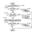
The treatment step of access device 100 sides at first, is described with Fig. 8.Among Fig. 8, at first, access device 100 sends the card type class to semiconductor memory card 111 and obtains order (S801) in order to obtain the card type category information of semiconductor memory card 111.Afterwards, utilize the order of sending, can judgement obtain card type category information (S802) from semiconductor memory card 111.Obtaining under the situation of failure, be judged as the generation mistake, end process (S803).Under the situation of achieving success, according to the information that obtains, judge whether to be and semiconductor memory card 111 is carried out access condition that the most suitable access uses and order (the most suitable access information is obtained order) the corresponding semiconductor memory card 111 (S804) of obtaining the access speed value of this moment from semiconductor memory card 111.If not corresponding semiconductor memory card 111 is then ended obtaining of access condition, access speed value, end process (S805).If corresponding semiconductor memory card 111 then sends the most suitable access information to semiconductor memory card 111 and obtains order (S806).Afterwards, utilize the order of sending to judge and to obtain access condition, access speed value (S807) from semiconductor memory card 111.Obtaining under the situation of failure, be judged as the generation mistake, end process (S808).Under the situation of achieving success, normal termination is handled.
Below, the treatment step of semiconductor memory card 111 sides is described with Fig. 9, Figure 10.The figure of the processing of semiconductor memory card 111 sides that Fig. 9 is expression when access device 100 sends card type class Fig. 8 explanation and obtains order.In the processing of semiconductor memory card 111 sides of Fig. 9, at first, semiconductor memory card 111 receives order (S901) from access device 100.Afterwards, with reference to the order that receives, judge whether be the improper order (S902) that self can't discern.Under the situation that is improper order, to access device 100 notification errors, end process (S903).Under the situation that is discernible order, judge whether this order is that the card type class obtains order (S904).Being that the card type class obtains under the situation of order order in addition, implement other processing (S905) corresponding to each order.Being that the card type class obtains under the situation of order, from card information storage part 132, read card type category information (S906).At last, the card type category information of reading is sent to access device 100, end process (S907).
The figure of the processing of semiconductor memory card 111 sides that Figure 10 is expression when access device 100 sends the most suitable access information Fig. 8 explanation and obtains order.In the processing of Figure 10, semiconductor memory card 111 receives order (S1001) from access device 100.Afterwards, with reference to the order that receives, judge whether be the improper order (S1002) that self can't discern.Under the situation that is improper order, to access device 100 notification errors, end process (S1003).Under the situation that is discernible order, judge whether this order is that the most suitable access information is obtained order (S1004).If not the most suitable access obtains order, then implement other processing (S1005), under the situation that is this order,, from card information storage part 132, read semiconductor memory card 111 is carried out the access condition and access speed value at this moment that the most suitable access is used at S1006.Afterwards, in S1007, access condition, the access speed value of reading sent to access device 100.
Like this, by the treatment step of Fig. 8-Figure 10 record, access device 100 can be obtained from semiconductor memory card 111 semiconductor memory card 111 is carried out the access condition and access speed value at this moment that the most suitable access is used.Figure 11 (a) is the figure of this access condition of expression, and Figure 11 (b) is the figure that the expression access speed is worth an example.Access condition is to handle unit sizes or handle the condition that the most suitable access, access device 100 should foundation is carried out in unit-boundary, access method, input clock frequency, bit amplitudes etc., expression for double conductor storage card 111 information shown in Figure 11 (a).Here, for example establishing and handling unit sizes is the multiple length of 128KB, and handling unit-boundary is the multiple length of 128KB, and access method is to the continuum consecutive access more than the 256KB, and input clock frequency is more than the 25MHz, and bit amplitudes is 4 bits.In addition, the access speed value is reading and writing, the information of the handling property when mean value, worst-case value etc., the expression access device 100 of wiping each transfer rate in handling carried out according to the access of formerly access condition shown in Figure 11 (b).By obtaining these information from semiconductor memory card 111, how access was better or obtain the access performance of which kind of degree this moment when access device 100 can be identified in this semiconductor memory card 111 carried out the most suitable access.Thus, can realize the most suitable access corresponding to the performance of semiconductor memory card 111.
Afterwards, as the 2nd method, illustrate that with reference to Figure 12, Figure 13, Figure 14 access device 100 returns the method for access speed value to semiconductor memory card 111 input access conditions, semiconductor memory card 111.Figure 12 is the figure of the processing of access device 100 sides in this method of expression.In the treatment step of access device shown in Figure 12 100 sides, the same with the situation of the 1st method shown in Figure 8, send the card type class and obtain order (S1201), if it is unsuccessful to give an order, the end that then makes mistakes (S1202, S1203).If success then in S1204, judges whether it is the correspondence card that the access speed value obtains order.If do not correspond to this order, then end obtain (S1205) of access speed value, if corresponding to this order, then in step S1206, send the access speed value and obtain order.Judge the whether success (step S1207) that obtains of access speed value, if unsuccessful, ends (S1208) that then make mistakes is as if obtaining then normal termination.In the method, because access device 100 becomes the order that has access condition in the independent variable to semiconductor memory card 111 input access conditions so the access speed value obtains order.
Below, the treatment step of semiconductor memory card 111 sides is described with Figure 13.The figure of the processing of semiconductor memory card 111 sides that Figure 13 is expression when access device 100 sends access speed value the explanation of Figure 12 and obtains order.If the processing of beginning Figure 13 then at S1301, receives order, judge whether it is improper order, if improper order, the end that then makes mistakes (S1302, S1303).If not improper order then judges whether be that the access speed value obtains order (S1304),, then implement other processing (S1305) if not should order.If the access speed value obtains order, then semiconductor memory card 111 is read access condition, access speed value (S1306) from card information storage part 132.Afterwards, with reference to access condition of reading and corresponding with it access speed value, access device 100 is judged the specified consistent access speed value (S1307) of access condition of independent variable that whether exists with order.Under non-existent situation, to access device 100 notification errors, end process (S1308, S1309).Under situation about existing, this access speed value is sent to access device 100, end process (S1310).
Like this, by the processing procedure of putting down in writing among Figure 12, Figure 13, access device 100 can be obtained the access speed value corresponding to this condition to semiconductor memory card 111 input access conditions.
Figure 14 (a) is the figure of the access condition of expression access device 100 input semiconductor memory cards 111, and Figure 14 (b) is the figure that access speed that expression semiconductor memory card 111 returns access device 100 is worth an example.The access condition of access device 100 input semiconductor memory cards 111 is shown in Figure 14 (a), be to establish that to handle unit sizes be 128KB, the processing unit-boundary is 128KB, access method is as coming consecutive access in the 256KB continuum, input clock frequency is more than the 25MHz, bit amplitudes is 4 than top grade, the information of the condition when expression is carried out access to semiconductor memory card 111.In addition, the access speed value shown in Figure 14 (b) is and the same information of Figure 11 (b) that expression is corresponding to the access speed value of the access condition of access device 100 inputs.Like this, the condition when semiconductor memory card 111 being carried out access by input, and obtain access speed value corresponding to this condition from semiconductor memory card 111, access device 100 can utilize the access method of supposition, judges the access performance that whether obtains expecting.
Below, the 3rd method is that access device 100 is imported the access speed values to semiconductor memory card 111, semiconductor memory card 111 returns the method for access condition.With Figure 15, Figure 16 this method is described.
Figure 15 is the figure of the treatment step of access device 100 sides in this method of expression.The processing of access device side is the same substantially with the action of the access device of above-mentioned the 2nd method, in the method, at step S1506, sends access condition and obtains order, replaces the access speed value among the step S1206 to obtain sending of order.
Figure 16 is the figure of the treatment step of semiconductor memory card 111 sides in expression this method.In the treatment step of Figure 16, be with the difference of the 2nd method that formerly illustrates, confirm whether be that access condition is obtained order at step S1604, afterwards, if should order, then from card information storage part 132, read access speed value (step S1606), replace the access speed value of step S1304 to obtain order.In addition, at step S1607,, judge whether there be the access condition consistent with the access speed value of access device appointment according to the access condition of reading.At S1608, if there is not this access condition, the end (S1609) that then makes mistakes if exist, then sends to access condition access device (S1610), end process.
By the processing procedure of putting down in writing among Figure 15, Figure 16, access device 100 can be imported the access speed values to semiconductor memory card 111, and obtains the access condition corresponding to this velocity amplitude.Access condition in this method, access speed value for example are the information shown in Figure 11 (b).In the method, desired performance number when so input is carried out access to semiconductor memory card 111 is obtained from semiconductor memory card 111 in order to satisfy the access condition that this performance number, access device 100 should foundations.Therefore, access device 100 can discern for meet the desired access performance, how semiconductor memory card 111 to be carried out access better, can realize expecting the access under the access performance.
Below, the 4th method is an access device 100 to semiconductor memory card 111 input access conditions, access speed value, can semiconductor memory card 111 return the method that satisfy the access speed value that is transfused under the situation with the access condition access of input.With Figure 17, Figure 18 this method is described.
Figure 17 is the figure of the treatment step of access device 100 sides in this method of expression.Among Figure 17, the same with the 1st method of explanation formerly, send the card type class and obtain order, if this achieves success, then judge it whether is card (S1704) corresponding to could the most suitable access decision order.If not should card, then ending could the most suitable access decision (S1705), if corresponding card, then in step S1706, sending could the most suitable access decision order.In the method, because access device 100 is to semiconductor memory card 111 input access condition and access speed values, so could the most suitable access decision order become the order that has access condition and access speed value in independent variable.Judge the whether success (S1707) that obtains of result of determination, if failure, if ends (S1708) that then make mistakes is success, then end.As the result of this order, the information that obtains from semiconductor memory card 111 under the situation of access under the access condition of appointment, whether satisfy the result of determination of the access speed value of appointment.
Below, the treatment step of semiconductor memory card shown in Figure 180 111 sides is described.The same with the 1st method, in this method, access device 100 also sends the card type class and obtains order, but the processing of semiconductor memory card 111 sides is the same with processing shown in Figure 9.Figure 18 be expression from access device 100 send the explanation of Figure 17 could be the most suitable the figure of processing of semiconductor memory card 111 sides during the access decision order.If the processing of beginning Figure 18 then receives order at S1801, judge whether it is improper order, if improper order, the end that then makes mistakes (S1802, S1803).If not improper order, then judge it whether is could the most suitable access decision order (S1804), if not should order, then implement other processing (S1805).If could the most suitable access decision order, then semiconductor memory card 111 be read access condition, access speed value (S1806) from card information storage part 132.Afterwards, with reference to the access condition read and corresponding with it access speed value, judge when access device 100 carries out access under the independent variable appointment access condition by order, whether satisfy the access speed value (S1807, S1808) of access device 100 appointments.Under the situation that satisfies the access speed value, satisfy access speed value, end process (S1809) to access device 100 notices.Under the situation that does not satisfy the access speed value, do not satisfy access speed value, end process (S1810) to access device 100 notices.
Like this, according to the treatment step of putting down in writing among Figure 17, Figure 18, access device 100 can be to semiconductor memory card 111 input storage condition and access speed values, and are identified under this condition whether to satisfy the access speed value when semiconductor memory card 111 carried out access.Access condition in this method, access speed the value for example information with shown in Figure 14 are the same.By this method, access device 100 can be identified under the access method of supposition whether meet the desired access performance before access.
Below, as the 5th method, the situation of performance about the sign of the speed ability grade in the information of the access speed of semiconductor memory card 111 of using is described.Both the access speed value of putting down in writing in this sign replacement the 1st method-the 4th method also can be contained in the access speed value as shown in Figure 7.The processing of one of processing of putting down in writing in the 1st method-the 4th method is used in memory storage 100 in this method, the processing between the semiconductor memory card 111.
Figure 19 (a) is the figure of an example of the speed ability grade determinating reference in this method of expression, and Figure 19 (b) is the figure of expression result of determination one example.The 5th information that speed ability grade determinating reference shown in Figure 19 (a) is used as in the card information storage part 132 is stored.Under the speed ability grade determinating reference shown in Figure 19 (a), the value of using during the mean value of use reading and writing, wiping each transfer rate in handling is used as judging, according to this determinating reference, corresponding to the access speed value, distribute the speed ability grade of one of " at a high speed ", " middling speed ", " low speed ".Equally, with regard to the worst-case value of transfer rate, also there is speed ability grade determinating reference.In the example of Figure 19 (b), distribute the speed ability grade of " at a high speed " to each access speed value.
In the method, so not only the access performance with semiconductor memory card 111 is divided into numerical value, also is categorized into objective grade, and memory storage 100 can be obtained grade from semiconductor memory card 111.Therefore, access device 100 can easily be discerned the access performance of semiconductor memory card 111.
Then, as the 6th method, the situation of the sign that uses the amount of power consumption grade in the information that shows the physical characteristics that is associated with semiconductor memory card 111 is described.Access device 100 is described to these signs of semiconductor memory card 111 input, obtains the access condition of correspondence and the method for access speed value with it.In the method, corresponding with the amount of power consumption grade in card information storage part 132, there is information about a plurality of access conditions and access speed value.
The processing of one of processing of putting down in writing in the 1st method-the 4th method is used in access device 100 in this method, the processing between the semiconductor memory card 111.Here, as an example, the situation that is applicable to the 1st method is described.The processing of access device 100 sides in this method is the same with treatment step shown in Figure 8.But difference is the amount of power consumption grade of additional performance amount of power consumption grade, and the most suitable access information that sends to semiconductor memory card 111 as access device among the S806 100 is obtained the independent variable of order.The amount of power consumption grade is taked following method, is about to watt level that semiconductor memory card 111 consumes and is divided into a plurality of grades and shows, and for example uses 3 stages such as " power consumption is big ", " in the power consumption ", " power consumption is little " to show etc.
Below, the treatment step of semiconductor memory card shown in Figure 20 111 sides is described.In this method, the processing of S2001-2005 is the same with the processing of the S1001-S1005 of semiconductor memory card shown in Figure 10 111 sides.If the most suitable access information is obtained order, then in S2006, judge that being appointed as the most suitable access information that sends from access device 100 obtains whether the amount of power consumption grade of the independent variable of order is effective value.If not effective value, then error process (S2007).If effectively, then in S2008, from card information storage part 132, read out under the amount of power consumption grade of appointment and carry out access condition, the access speed value that the most suitable access is used.Afterwards, the information of reading is sent to access device 100, end process (S2009).That is, in the method, suppose to have a plurality of information that are stored in the card information storage part 132, select to send to access device 100 corresponding to information from the amount of power consumption grade of access device 100 appointments corresponding to the amount of power consumption grade.
In the method, so when semiconductor memory card 111 is obtained information about access speed, the information of the access speed of access device 100 when semiconductor memory card 111 specifies the value of the amount of power consumption grade of performance hypothesis, access device 100 to obtain to operate under the amount of power consumption of appointment about semiconductor memory card 111.Thus, for example want to drive under the situation of semiconductor memory card 111, can discern the access speed value of essential access condition or this moment with low-power consumption at access device 100.
In addition, the same with the 1st method here, with the sign input semiconductor memory card 111 of power, obtain corresponding with it access condition and access speed value, but shown in the 2nd method, except that access condition, the grade of amount of power consumption also is shown to storage card, obtains corresponding with it access speed.In addition, shown in the 3rd method, except that access speed, also, obtain corresponding with it access condition to the sign of semiconductor memory card 111 input expression amount of power consumption grades.In addition, shown in the 4th method, except that access condition, access speed, the sign of input expression amount of power consumption, whether people's semiconductor memory card 111 is satisfied the result of this condition.
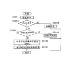
Below, the 7th method is in response to the request of access device 100, and semiconductor memory card 111 returns the method for the MIN information essential in order to calculate the access speed value to access device 100.With Figure 21-Figure 25 this method is described.At this moment, the content of the access performance Back ground Information table (APBIL) that shows under also can in the card inter-process time shown in Figure 7 of card information storage part 132 shown in Figure 7, keeping.
Figure 21 is the figure of the treatment step of access device 100 sides in expression this method, and Figure 22 is the figure of the treatment step of expression semiconductor memory card 111 sides.In the treatment step of access device shown in Figure 21 100 sides, at first to send the card type class and obtain order (S2101), judgement obtains whether success (S2102).If unsuccessful, then carry out the end (S2103) that makes mistakes, if success then at S2104, judges whether it is the card of obtaining order corresponding to access performance Back ground Information table.If not should the correspondence card, then S2105 ends obtaining of access performance Back ground Information table.If corresponding card then sends access performance Back ground Information table at S2106 and obtains order.In addition, judge the whether success (S2107) that obtains of this information table,, then carry out the end (S2108) that makes mistakes if obtain failure.If achieving success of this information table, then S2109 calculates the access speed value according to this information table.In the step of S2010,, calculate in order to satisfy the required required access condition of access speed of this access device 100 according to the access speed value of calculating.After the treatment step of semiconductor memory card 111 sides in explanation this method, this two steps are described with accompanying drawing.
Below, the treatment step of semiconductor memory card shown in Figure 22 111 sides is described.The same with the 1st method, in the method, access device 100 also sends the card type class and obtains order, but the processing of semiconductor memory card 111 sides is the same with processing shown in Figure 9.The figure of the processing of semiconductor memory card 111 sides that Figure 22 is expression when access device 100 sends access performance Back ground Information table the explanation of Figure 21 and obtains order.In the processing of Figure 22, receive order (S2201), if improper order, the end that then makes mistakes (S2202, S2203).If not improper order then checks whether be that access performance Back ground Information table is obtained order in S2204.If not should order, then implement other processing (S2205), from card information storage part 132, read access performance Back ground Information table and obtain order (S2206, S2207).
Below, illustrate that with Figure 23, Figure 24, Figure 25 access performance Back ground Information table obtains order and use this to show to calculate the method for access speed value.Figure 23 is the figure that expression semiconductor memory card 111 returns to access performance Back ground Information table (PABIL) example of access device 100.Figure 24, Figure 25 are the order between expression access device 100 and the semiconductor memory card 111, the figure of response timing one example.As the numerical value of access performance of expression semiconductor memory card 111, transfer rate etc. for example.But, the factor of determining the transfer rate between access device 100, the semiconductor memory card 111 does not exist only in the semiconductor memory card 111, also be present in access device 100 sides, so in order to derive actual transfer rate, the essential condition that increases access device 100 sides.In the method, access device 100 can be obtained about the access performance of the semiconductor memory card 111 sides information of determining cause element really, adds the factor of access device 100 sides, and access device 100 can be calculated access speed.
Figure 23 is the figure of expression conduct about access performance Back ground Information table (PABIL) example of the information of the factor of semiconductor memory card 111 sides of definite access performance.As shown in the figure, each reading and writing and wipe processing form 1-A, 1-B, 1-C are all arranged.Holding time when per 512 byte datas transmission in the processing is write in Figure 23 (b) expression.In this information table,, the table that changes owing to the variation of handling unit sizes, consecutive access (SA) or random access (RA) is shown as the factor that the processing time changes.
Below, the method for calculating the access speed value according to access performance Back ground Information table shown in Figure 23 is described.Figure 24, Figure 25 are the order between expression access device 100 and the semiconductor memory card 111, the figure of response timing one example.Figure 24 (a) handles corresponding to reading, and Figure 24 (b) is corresponding to writing processing, and Figure 25 is corresponding to wiping processing.The total of sending processing time RT1, card inter-process time RT2, data transmission period RT3 according to order is calculated the access speed value in handling read of Figure 24 (a).Here, RT1, RT3 depend on the clock frequency of access device 100 input semiconductor memory cards 111 and definite time, and access device 100 sides can be calculated the time.On the other hand, RT2 is card inter-process institute's time spent, depends on that semiconductor memory card 111 is definite.Therefore, the access performance Back ground Information table of obtaining from semiconductor memory card 111, the required information of this RT2 is determined in storage.
Equally, the total of sending processing time WT1, card inter-process time WT2, data transmission period WT3 according to order is calculated the access speed value in the processing write of Figure 24 (b).Therefore, and read to handle the same, in access performance Back ground Information table, storage determines to block the required information of inter-process time WT2.
Equally, the total of sending processing time ET1, card inter-process time ET2 according to order is calculated the access speed value in the processing of wiping of Figure 25.Therefore, and read to handle the same, in access performance Back ground Information table, storage determines to block the required information of inter-process time ET2.
Here, will write processing, the example of calculating of access speed value will be described as an example.Calculate unit sizes data processing institute's time spent (write the time entirely: WT_A), as the access speed value.WT A can be obtained by following formula (1).
WT_A=WT1+∑WT2+∑WT3…(1)
Here, obtain from the input command to the response that to finish required volume of transmitted data be 160 bits establishing, input clock frequency is under the situation of sMHz, and order is sent processing time WT1 and can be obtained by following formula (2).
WT1=160/(s×POW(10,6))…(2)
Here, POW (X, Y) the Y power of expression X.
Below, ∑ WT2 is a card inter-process institute time spent summation, and the holding time of record is t (second) in establishing Figure 24 (b), and the processing unit sizes is under the situation of n (byte), can be obtained by following formula (3).
∑WT2=t×n/512…(3)
Below, ∑ WT3 is the summation of data transmission period, use 4 bits to be used as bit amplitudes, will for the legitimacy of confirming to transmit data and the total transfer clock number during the data addition of additional CRC and 512 bytes be made as under the situation of 1049 clocks, can obtain by following formula (4).
∑WT3=(1049×n/512)/(s×POW(10,6))
…(4)
Therefore, as an example of calculating, be that 25MHz, processing unit sizes are under the situation of 128KB, consecutive access at the hypothesis input clock frequency, t is 9.2 microseconds, WT_A calculates and is 13.1ms.
In the method, so obtain information about the factor of semiconductor memory card 111 sides of determining access speed, the access performance that output is corresponding with it from access device 100.Therefore, access device 100 factor that can increase access device 100 sides is calculated access speed.
Below, the 8th method is that the guide look of the access speed value under the various access conditions is remained in the card information storage part 132, in response to request from access device 100, and the method that semiconductor memory card 111 returns.With Figure 26-Figure 28 this method is described.
Figure 26, Figure 27, Figure 28 are the figure of an example of the access performance table of maintenance in the expression semiconductor memory card 111.Figure 26 (a) illustrates the accessible data size of time per unit to each input clock, and Figure 26 (b) by each access unit, is shown specifically standard value and worst-case value to consecutive access and random access to its part.In addition, Figure 27 (a) is by to reading to handle, write processing, wiping and handle the required time of data processing that each different input clocks illustrates unit sizes.Figure 27 (b) is writing processing and then to the required time of the data processing of unit sizes, by each processing unit sizes, consecutive access and random access being shown specifically standard value and worst-case value of 25MHz to its a part of input clock.Processing speed when Figure 28 (a) shows as access performance with the unit sizes access to each input clock, illustrates and reads to handle, write processing, wipes the form under handling.In addition, Figure 28 (b) is a part of for it, is 25MHz at input clock, writes under the situation of processing, handles unit sizes by each, and consecutive access and random access are shown specifically standard value and worst-case value.These information are the technique of expression difference of access performance only, but is the information of the access speed of performance semiconductor memory card 111.
Figure 29 is the figure of the treatment step of access device 100 sides in expression this method, and Figure 30 is the figure of the treatment step of expression semiconductor memory card 111 sides.Access device 100 at first sends the card type class and obtains order (S2901) as shown in figure 29, judges the whether success (S2902) that obtains of this card type class.If this is wrong in obtaining, the end (S2903) that then makes mistakes if achieve success, then in S2904, judges whether it is the correspondence card that the access performance table is obtained order.If not should the correspondence card, then end obtain (S2905) of access performance table, if corresponding card then sends the access performance table and obtains order (S2906).In addition, in S2907, judge whether obtaining of access performance table be successful, if mistake, end (S2908) then makes mistakes.If achieving success of access performance table then in S2909, according to the access performance table, determined access condition, end process.
If semiconductor memory card 111 receives order, as shown in figure 30 improper order, then error process (S301-S3003).Judge whether it is that the access performance table is obtained order (S3004).If not should order, then end obtain (S3005) of access performance table, if should order, then from card information storage part 132, read access performance table (S3006).In addition, in S3007, send access performance table, end process to access device.
That is, the difference of this method and the 7th method is, access device 100 is obtained information about access speed from semiconductor memory card 111, so access device 100 sides needn't be calculated access speed.In the method, access device 100 is so obtained these access performance tables, can discern to the guide look of the access condition of semiconductor memory card 111 and under each access condition the access speed value during access.Thus, access device 100 can be identified under the access condition of self hypothesis the access speed value during access for what or in order to satisfy self required access speed value, to be preferably in to carry out access under what access condition.
As mentioned above, keep access performance when 100 pairs of semiconductor memory cards of access device 111 carry out access in the card information storage part 132 of the semiconductor memory card 111 of present embodiment in semiconductor memory card 111.Semiconductor memory card 111 is in response to the request from access device 100, and part or all of this information sent to access device 100.Thus, access device 100 is known the access performance of semiconductor memory card 111.Therefore, access device 100 can optimal access method come semiconductor memory card 111 is carried out access, can bring into play the peak performance of semiconductor memory card 111.
In addition, the information that is stored in the card information storage part 132 is renewable respectively.For example, by from speed ability grade determinating reference and the renewal shown in outside input Figure 19 (a) of semiconductor memory card 111, can change determinating reference subsequently.In addition, as other example, because the internal state change of semiconductor memory card 111, under situation about the information change of access performance, monitors internal state in semiconductor memory card 111, corresponding to the variation of internal state, change is about the information of access performance.In addition, in the present embodiment, put down in writing whole processing of access device 100 sides begin carry out the example that the kind of semiconductor memory card 111 is judged, judge but also can when at first semiconductor memory card 111 being carried out access, only carry out a kind.In addition, needn't use the full detail shown in Fig. 7, and only use a part, also a part and the out of Memory combination of the information shown in Fig. 7 can be used afterwards about access performance.In addition,, put down in writing the example that is divided into 3 kinds of grades respectively, but also may be partitioned into multiple beyond 3 kinds as speed ability grade, amount of power consumption grade.In addition,, 3 kinds of examples of Figure 26, Figure 27, Figure 28 are shown, but so long as the information of the access performance of expression semiconductor memory card 111 then also can be used other form of expression, in addition, these a plurality of forms of expression also capable of being combined are used as the access performance table.In addition, the 1st storer 118 of storage card information is illustrated as renewable nonvolatile memory, but under news more, also can uses nonupdatable nonvolatile memories such as ROM.In addition, also can be not at the 1st storer 118 and at nonvolatile memory 117 stored card informations.
(embodiment 2)
In embodiments of the invention 2, illustrate from the semiconductor memory card that possesses the card information storage part and obtain information, and be used for the access device of the file system control of access device about the access performance of semiconductor memory card.
Semiconductor memory card in the present embodiment is the same with formation shown in Figure 1 with the formation of access device.In the present embodiment, especially describe file system control unit 106, access condition determination portion 107, card information obtaining section 108, card service condition storage part 110 among the ROM104 in the access device 100 in detail.
Before the detailed description in carrying out present embodiment,, be that example describes with the FAT file system as being used for the file system of managed storage in the data of semiconductor memory card 111.Figure 31 illustrates the formation of FAT file system.The file system management of Figure 31 zone 117-A is meant the zone by the file system management in the nonvolatile memory 117 in the semiconductor memory card 111, is equivalent to be recited as among Fig. 1 the Zone Full or the subregion in the zone of user data 131.In addition, among Figure 31, LA presentation logic address.In the FAT file system, in the beginning of file system management zone 117-A, there is the management information areas 3001 of the integral body that is used for managing file system management area 117-A, there is the data area 3002 of data in the storage file etc. afterwards.Management information areas 3001 by Main Boot Record allocation table (below be called MBR.PT) 3003, distribute boot sector (below be called PBS) 3004, document alignment table (below be called FAT) 3005,3006, root directory item (below be called RDE) 3007 to constitute.
MBR.PT3003 is that storage becomes a plurality of parts that assigned region is managed the information of usefulness that are called with the file system management Region Segmentation.PBS3004 is the part of the management information in 1 distribution of storage.FAT3005, the 3006th, expression is contained in the part of the physical storage locations of the data in the file.RDE3007 is the part that is present in the information of file under the root directory, catalogue.In addition, FAT3005, the 3006th, expression is contained in the important area of physical storage locations of the data in the file, thus usually at the file system management region memory at two FAT3005,3006 with identical information, carry out dualization.
Below, with Figure 32 data storage example in the FAT file system is described.Data area 3002 is managed by the regular length block unit that is called bunch, gives bunch sequence number since 2 ascending order to each bunch.The behaviour in service of FAT3005,3006 each bunches of management, represent to constitute the link information of the contact between each bunch by FAT item corresponding to each bunch sequence number.The FAT item is because the kind difference of FAT file system, is arbitrary size in each bunch 12 bits, 16 bits, 32 bits 3 kinds.In the example of Figure 32, illustrate and show 1 situation with 16 bits.In the FAT item, storage connect down bunch bunch sequence number, represent this bunch be dummy section 0x0000, represent that this bunch is the value that links one of 0xFFFF of terminal.Part shown in the enlarged drawing middle probe 2-7 of Figure 32 is represented the FAT item at bunch sequence number 2-7.In this example, in the FAT item corresponding to bunch sequence number 2,5,7, storage 0x0000 represents that these 3 bunches is dummy section.In addition, in FAT item corresponding to bunch sequence number 3, storage 0x0004, in FAT item corresponding to bunch sequence number 4, storage 0x0006, in FAT item corresponding to bunch sequence number 6, storage 0xFFFF, expression is cut apart the storage data for 3 bunches to bunch sequence number 3,4,6 etc.
Below, the example that writes of file data in the FAT file system is described with Figure 33, Figure 34, Figure 35.Figure 33 is the process flow diagram that expression writes processing, and Figure 34 is the figure that expression writes an example of handling preceding directory entry 3301, FAT3005,3006, data area 3002.Figure 35 is the figure that expression writes an example of directory entry 3301 after the processing, FAT3005,3006, data area 3002.In the FAT file system, in the part of root directory item 3007 or data area 3002, store storage the directory entry 3301 of filename or information such as document size, file attribute.Figure 34 (a) illustrates an example of directory entry 3301.The file of the file shown in this directory entry 3301 is called FILE1.TXT, from the data of a bunch sequence number (C1.NO.) 10 beginning storage files.Document size is 60000 bytes.The FAT data instance of the corresponding bunch sequence number 9-14 of Figure 34 (b) expression.In addition, Figure 34 (c) is assumed to be 16384 bytes with 1 bunch size, in 4 bunches of bunch 10-13, and the data of storage file FILE.TXT.
Figure 33 is the figure of the treatment step that writes of the file data in the expression FAT file system.Come the supporting paper data to write processing with Figure 33.Write in the processing at file data, at first read in the directory entry 3301 (S3301) of obj ect file.Afterwards, obtain the file that is stored in the directory entry 3301 that reads in and begin a bunch sequence number, confirm the beginning position (S3302) of file data.Afterwards, read in FAT3005,3006, the position of the switch of the file data of obtaining from S3002, order links on FAT3005,3006, obtains bunch sequence number (S3303) of writing position.Afterwards, whether when writing data, judging needs to redistribute dummy section (S3304) to file.Under the situation that needn't distribute dummy section, advance to the processing of S3306.Distribute at needs under the situation of dummy section, on FAT3005,3006, retrieve dummy section, 1 bunch dummy section is distributed to the end (S3305) of file.Afterwards, with only write current reference bunch in data write data area 3002 (S3306).Afterwards, judge write (S3307) that whether finishes total data.In addition, under the situation of remaining data, return the processing of S3304.Finish under the situation about writing of total data, updating stored in document size in the directory entry 3301 or time tag etc., writing (S3308) in the semiconductor memory card 111.At last, FAT3005,3006 is write in the semiconductor memory card 111, finish processing (S3309).
Write processing by this document data, under situation the about further data of 1000 bytes being write among the file FILE1.TXT with 60000 byte datas shown in Figure 34, as shown in figure 35, in bunch sequence number C1.No14, write new data, be changed to file with 70000 byte datas.
Like this, in the FAT file system,, carry out region allocation, the storage data with a bunch unit as the storage area of file data.In addition, a plurality of bunches that distribute to 1 file needn't be continuous, might distribute discontinuous zone.Under the poorest situation, in cutting apart the discontinuity zone of cluster unit, write file data.At this moment, 1 access size of semiconductor memory card 111 is become size below 1 bunch, for semiconductor memory card 111 being carried out under the required access unit of the access situation bigger than bunch size, can not come access with the peak performance of semiconductor memory card 111 with the most at a high speed.
In the present embodiment, provide following method, promptly obtain information, be used for the processing of file system, thus, come semiconductor memory card 111 is carried out file access with optimal access method about access performance from semiconductor memory card 111.
Below, definite processing of the file-system access unit in the present embodiment is described.Called file system access unit (below be called FS access unit) and management unit bunch different of carrying out district management usually as file system are newly-installed management units in the present embodiment.Bunch size be provided with higher limit owing to the interchangeability of the equipment room that uses file system, can not easily change size.But, in order semiconductor memory card 111 to be carried out the high limit of size that the required access unit of the most suitable access is not limited to bunch with interior size.Therefore, in the present embodiment, except that bunch, also be provided with according to information new district management unit that set, that be called FS access unit about the access performance obtained from semiconductor memory card 111, be used for the processing of file system.Like this, can in the interchangeability of maintenance and existing file system, realize access corresponding to the characteristic of semiconductor memory card 111.
Definite processing of the FS access unit in the present embodiment is described with Figure 36.Figure 36 is expression file system control unit 106 obtains treatment step one example of FS access unit from access condition determination portion 107 figure.Among Figure 36, at first obtain FS access unit (S3601) to 107 requests of access condition determination portion from file system control unit 106.Afterwards, obtain card information (S3602) from access condition determination portion 107 to 108 requests of card information obtaining section.Afterwards, use arbitrary method of explanation among the embodiment 1, card information obtaining section 108 obtains card information (S3603) from semiconductor memory card 111.Under the situation that obtains failure of card information, from card information obtaining section 108 via access condition determination portion 107 to file system control unit 106 notification errors, end process (S3604, S3605).Under the situation of achieving success, send card information (S3606) to access condition determination portion 107 from card information obtaining section 108.Afterwards, the access condition of access condition determination portion 107 when card service condition storage part 110 is obtained 100 pairs of semiconductor memory cards of access device 111 and carried out access or the card service condition (S3607) of the information such as access speed value of expectation.Afterwards, relatively card information, card service condition judge whether there is the processing unit sizes (S3608) that is suitable for the card service condition.Can not satisfy situation of the access speed value shown in the card service condition etc. at semiconductor memory card 111, not exist under the situation of suitable processing unit sizes, to file system control unit 106 notification errors, end process (S3609, S3610).Under the situation that has suitable processing unit sizes, should handle unit sizes and be defined as FS access unit, send to file system control unit 106 from access condition determination portion 107, end process (S3611).
Like this, in the present embodiment, relatively card information and card service condition are determined FS access unit, as the most suitable access unit that semiconductor memory card 111 is carried out access.For example shown in Figure 28 (b), supposing following semiconductor memory card 111, is 25MHz at input clock, when writing in the processing consecutive access, in the access of 16KB unit, the access performance of 6MB/s becomes standard value, and in the access of 128KB unit, the access performance of 10MB/s becomes standard value.Here, need at access device 100 under the situation of access performance of 8MB/s FS access unit to be defined as 128KB.In addition, by coming semiconductor memory card 111 to be carried out access, the access performance that can obtain expecting by each FS access unit.
In addition, as an example of card service condition, enumerate access condition shown in Figure 14 and access speed value.Promptly, the access condition of Figure 14 (a) is the information of expression about the condition of the access method of 100 pairs of semiconductor memory cards of access device 111 hypothesis, and the access speed value shown in Figure 14 (b) is the value of the access performance obtained when under this condition semiconductor memory card 111 being carried out access.Keep these information about access performance by access device 100, decidable semiconductor memory card 111 can satisfy the access performance that oneself requires.
In addition, treatment step shown in Figure 36 be shown in embodiment 1 the 1st method like that, access device 100 for input the treatment step during about the information of access condition, access speed value.Shown in the 2nd method shown in embodiment 1, under the situation of access device 100 essential input access conditions, in the processing of Figure 36, between step S3601 and S3602, the condition storage part 110 that additional access condition determination portion 107 is used from card is obtained the card service condition and is notified to the step of card information obtaining section 108.
Below, explanation will be used for the SOME METHODS of the processing of file system by the FS access unit that treatment step shown in Figure 36 is determined.
As the 1st method, the method for utilizing FS access unit to come the formatted file system is described.Configuration example when Figure 37 represents to come the formatted file system according to FS access unit.FS access unit is 128KB here, is set at the multiple length of bunch size.Here, be made as 16KB with 1 bunch.In Figure 37, management information areas 3001 is MBR.PT3003, FAT3005,3006, RDE3007.In the present embodiment, set the size of adjusting management information areas 3001 for, with the M multiple length (M is an integer) that becomes FS access unit.Here, management information areas 3001 is crossed over two FSAU-S0 of FS access unit, FSAU-S1 and is used 512 sectors (S) as shown in the figure.
Thus, the beginning of data area 3002 is consistent with FS access unit-boundary, and the district management of later data area 3002 can be realized by FS access unit without difficultyly.In addition, be the multiple length of bunch size because FS access unit is set at, so can in the district management in pressing FS access unit multiple length execution data area 3002, integrate with the district management of bunch unit.
Below, as the 2nd method, the file data wiring method according to FS access unit is described.Figure 38 is the figure that the file data in expression this method writes treatment step.Write in the processing at file data, at first judge whether exist the above residue of FS access unit length to write data length (S3801).Under the situation of not enough FS access unit length, advance to the processing of S3808.Being under the situation more than the FS access unit length, before writing semiconductor memory card 111, generate the data (S3802) of FS access unit length.Afterwards, each FS access unit length is retrieved dummy section on FAT3005,3006, obtaining the zone that is contained in the FS access unit all is the zone (S3803) of dummy section.Under the situation that does not have dummy section, notification error, end process (S3804, S3805).Exist under the situation of dummy section, the data of FS access unit length are being write (S3806) in the dummy section of obtaining together.Afterwards, judge write (S3807) that whether finishes total data.Do not finish under the situation about writing, returning the processing of S3801.Finish under the situation about writing end process.In addition, in S3801, be judged to be under the situation of remaining data curtailment FS access unit, generate the remaining data (S3808) of not enough FS access unit.Afterwards, the same with the step of S3803, obtaining the zone that is contained in the FS access unit all is the zone (S3809) of dummy section.Under the situation that does not have dummy section, notification error, end process (S3810, S3811).Exist under the situation of dummy section, remaining data is being write together in the dummy section of obtaining, end process (S3812).
Here, write in the processing, under the situation of the dummy section that does not have FS access unit, will write processing and be made as mistake, but also can obtain the following dummy section of FS access unit, and write data at file data.
Figure 39 is the figure of user mode one example of expression data area.In this example, in the FSAU-0 of FS access unit, write the data of file FILE1, in the FSAU-1 of FS access unit, write the information of catalogue DIR1.Becoming under the situation of this data configuration, in the method, selecting the zone (bunch sequence number is from the zone of C1.No18 to 25) of the FS FSAU-2 of access unit, writing the zone as file data.That is, even there is 1 bunch, file data write area territory also need not be done in the zone of existing FS FSAU-0 of access unit or FS storage cell FSAU-1 to the information of file data or catalogue in FS access unit.Therefore, have the to a certain degree file data of the document size of size relatively, the continuum that must guarantee FS access unit is so can optimal access unit carry out zero access to semiconductor memory card 111.
Below, as the 3rd method, the directory area distribution method according to FS access unit is described.Figure 40, Figure 41 are the procedure charts of the directory area allocation process in expression this method.In the directory area allocation process, at first current reference position (S4001) is set in beginning in the data area.Afterwards, judge in the FS of current reference access unit, whether there is directory area (S4002).Under non-existent situation, advance to the processing of S4005.Under situation about existing, judge in the FS access unit of current reference whether have empty bunch (S4003).Not existing under empty bunch the situation, advance to the processing of S4005.Exist under empty bunch the situation, should sky bunch distributing to directory area, end process (S4004).In S4002, S4003, judge under the situation do not have the zone, whether judge data zone 3002 whole have been finished affirmation (S4005).Under uncompleted situation, current reference position is set at next FS access unit (S4006), return the processing of S4002.
Under situation about finishing, among Figure 41, obtain the zone that is contained in the FS access unit from total data zone 302 and all be empty bunch zone (S4007) to the affirmation of Zone Full.Exist under the situation of dummy section, a sky that is contained in the zone of obtaining bunch is being distributed to directory area, end process (S4008, S4009).Under the situation that does not have dummy section, from the total data zone, obtain empty bunch (S4010).There are not under empty bunch the situation notification error, end process (S4011, S4012).Exist under the situation of dummy section, the sky obtained bunch is being distributed to directory area, end process (S4013).
Figure 42 is the figure of user mode one example of expression data area.As shown in figure 42, data configuration comprises directory area for to comprise data in the FSAU-0 of FS access unit in bunch sequence number 10,11 of the FSAU-1 of FS access unit.At this moment, in the method, the sky in being contained in the FSAU-1 of FS access unit bunch, promptly bunch sequence number 12-17 distributes catalogue.Like this, by distributing directory area, directory area preferentially is stored in the same FS access unit, the result is easy to generate the dummy section of FS access unit length.Thus, effectively guaranteed continuum based on the file data of the 2nd method.
Afterwards, as the 4th method, the denotation approach of carrying out according to FS access unit of going is described.It is following processing that what is called is removed sign, promptly the file data of decentralized configuration in recording medium is disposed again, to make it to be configured in the continuum, file data is carried out zero access.In the method, go in the sign processing, carry out the sign that goes according to FS access unit at this.Figure 43 is the figure that expression goes to indicate data configuration one example before handling.In this example, in any of 3 FSAU-0 of FS access unit, FSAU-1, FSAU-2, all store file data or catalogue.Therefore, in the dummy section of the FS of the 2nd method access unit is obtained, can not obtain dummy section.Here, utilize the sign that goes of having considered FS access unit to handle, the directory area that is contained among the FSAU-2 of FS access unit is moved in the sky bunch zone of the FSAU-1 of FS access unit, directory area is pooled to the FSAU-1 of FS access unit.Represent this processing by (1).In addition, the data of the file (FILE2) of the FSAU-2 of FS access unit are moved in the sky bunch zone of the FSAU-0 of FS access unit, file data is pooled to the FSAU-0 of FS access unit.Represent this processing by (2).As a result, change to data configuration shown in Figure 44, the FSAU-2 of FS access unit all becomes dummy section, can utilize the dummy section of the FS access unit in the 2nd method to obtain, and is assigned as the dummy section that file data is used.
That is, in the method, going during sign handles, directory area is being pooled in the same FS access unit, again the file data of not enough FS access unit sizes is being pooled in the same FS access unit, generating the dummy section of FS access unit multiple length thus as far as possible.Thereby, can effectively guarantee continuum based on the file data of the 2nd method.In addition, the Zone Full that is used for file data storage etc. in will recording medium merges to a continuum, dummy section integral body is made as the continuum, carries out all the time and remove to indicate the dummy section of processing, can shorten sign and handle institute's time spent with generation FS access unit multiple length.
Afterwards, as the 5th method, explanation obtains the method for the residue dummy section length of FS access unit.Figure 45 is the figure that the residue dummy section length in this method of expression obtains processing procedure.Obtain in the processing in residue dummy section length, at first empty FS access units is made as 0 (S4501).Afterwards, current reference position is set at data area beginning (S4502).Afterwards, judge in the FS access unit of current reference whether all be empty bunch (S4503).All being under empty bunch the situation, make sky FS access units add 1 (S4504).Judge the affirmation of whether finishing Zone Full (S4505) afterwards.Under uncompleted situation, current reference position is set at next FS access unit, and returns the processing (S4506) of S4503.Under situation about finishing, the numerical value that is stored in the sky FS access units is converted into byte number, be notified to application program 105, end process (S4507).
Here, obtain in the processing, illustrate residue dummy section length is converted into the example of notifying behind the byte number, but if can correctly discern residue dummy section length, notify after also can be converted into sector number or number of clusters in residue dummy section length.
Figure 46 is the figure of data configuration state of expression data area 3002, in representing to use with shade bunch.Under the situation that constitutes such data configuration, obtain in the processing in the residue dummy section length of this method, as shown in the figure, there are 3 empty continuums (SEE).Therefore, the Zone Full in the FS access unit is judged to be dummy section for empty bunch 3 FSAU-1 of FS access unit, FSAU-3, FSAU-5.
In the method, the number of the dummy section by so calculating FS access unit length also is notified to application program 105, and application program 105 can be discerned the residue dummy section length of FS access unit.Thus, each FS access unit is carried out when satisfying the access of required access performance, can utilize this access performance only to write or discern remaining data at access device 100.
As mentioned above, the access device 100 among the embodiment 2 is obtained information about access performance from semiconductor memory card 111, determines optimal access unit, uses this access unit in the processing of file system.Thus, access device 100 can optimal access method carry out access to semiconductor memory card 111, can bring into play the peak performance of semiconductor memory card 111.
In addition, in embodiment 2, put down in writing all and realized the example of file system control unit below 106, but also all or part of hardwareization of these functions can be additional on the access device 100 by the program on the ROM104 of access device 100.For example shown in Figure 47, in ROM104, only there is application program 105, hardware file system control unit 106, access condition determination portion 107, card information obtaining section 108, access control portion 109, condition storage part 110, as semiconductor storage card control LSI4701, be additional on the access device 100.The example that constitutes shown in Figure 47, also only hardwareization by semiconductor memory card control LSI4701 being set FS access unit, making later data transmission to semiconductor memory card 111 carry out the part of the function that illustrates in function that data send etc., the present embodiment automatically according to FS access unit.In addition, in the present embodiment the FAT file system is illustrated as an example of file system, but so long as management unit's size of each regulation is carried out the file system of district management, then also can use other file system such as UDF.
Utilizability on the industry
Semiconductor memory card of the present invention, access device and access method are by optimization access dress Put one of side, semiconductor memory card side or both processing, can realize semiconductor memory card Zero access. This semiconductor memory card, access device or method can be used for semiconductor storage Card is as among the digital AV equipment of recording medium or mobile telephone, digital camera, the PC etc. In addition, at the recording medium and the equipment that are used for the high high-quality AV data of record transfer rate Situation under, the most suitable utilization.
Claims (18)
1. one kind is connected to the semiconductor memory card that uses on the access device, it is characterized in that, comprising:
Main interface portion transmits control signal and data to access device, and receives the signal from access device;
Nonvolatile memory is grouped into erase block as the least unit of data erase with a plurality of continuous sectors;
Memory Controller, control to the data erase of described nonvolatile memory, write, read;
Card information storage storer, comprise the information relevant of storage at least, access condition and about the card information storage part of the information of access performance with described semiconductor memory card internal physical characteristic, wherein said access condition is the condition when described access device carries out access to described semiconductor memory card, and described access performance is the access performance of described semiconductor memory card performance when described access device is carried out access according to described access condition; With
According to the control part of controlling each one through the resulting control signal of described main interface portion, described control part is corresponding to the information relevant with the access speed of described access device appointment, from described card information storage part, read access condition to the described semiconductor memory card relevant information required, and send it to described access device with satisfying described access speed.
2. one kind is connected to the semiconductor memory card that uses on the access device, it is characterized in that, comprising:
Main interface portion transmits control signal and data to access device, and receives the signal from access device;
Nonvolatile memory is grouped into erase block as the least unit of data erase with a plurality of continuous sectors;
Memory Controller, control to the data erase of described nonvolatile memory, write, read;
Card information storage storer, the card information storage part of the information that the access speed that described semiconductor memory card is brought into play when comprising the information relevant with described semiconductor memory card internal physical characteristic of storage at least, access condition and carrying out access according to described access condition with described access device is relevant, wherein said access condition are the conditions when described access device carries out access to described semiconductor memory card; With
According to the control part of controlling each one through the resulting control signal of described main interface portion, when described control part carries out access to described semiconductor memory card read information and information relevant with the access condition of described access device appointment from described card information storage part after, under described access condition about access speed, judge whether satisfy described access speed, and result of determination is sent to described access device.
3. one kind is connected to the semiconductor memory card that uses on the access device, it is characterized in that, comprising:
Main interface portion transmits control signal and data to access device, and receives the signal from access device;
Nonvolatile memory is grouped into erase block as the least unit of data erase with a plurality of continuous sectors;
Memory Controller, control to the data erase of described nonvolatile memory, write, read;
Card information storage storer, comprise storage and the relevant information of described semiconductor memory card internal physical characteristic at least, access condition and as about the information of access performance, the card information storage part of the information relevant with the access speed of described nonvolatile memory, wherein said access condition is the condition when described access device carries out access to described semiconductor memory card, described access performance is the access performance of described semiconductor memory card performance when described access device is carried out the access of the described access condition of foundation, and described access speed is the access speed of described nonvolatile memory under a plurality of grades of the amount of power consumption of described semiconductor memory card; With
According to the control part of controlling each one through the resulting control signal of described main interface portion, described control part is in response to from the request of described access device and the appointment of amount of power consumption grade, from described card information storage part, read and be used for that described semiconductor memory card is carried out relevant information of the access condition of access and the relevant information of access speed when under described access condition semiconductor memory card being carried out access, and send it to described access device.
4. one kind is connected to the semiconductor memory card that uses on the access device, it is characterized in that, comprising:
Main interface portion transmits control signal and data to access device, and receives the signal from access device;
Nonvolatile memory is grouped into erase block as the least unit of data erase with a plurality of continuous sectors;
Memory Controller, control to the data erase of described nonvolatile memory, write, read;
Card information storage storer, comprise storage and the relevant information of described semiconductor memory card internal physical characteristic at least, access condition and as about the information of access performance, the card information storage part of the information relevant with the access speed of described nonvolatile memory, wherein said access condition is the condition when described access device carries out access to described semiconductor memory card, described access performance is the access performance of described semiconductor memory card performance when described access device is carried out the access of the described access condition of foundation, and described access speed is the access speed of described nonvolatile memory under a plurality of grades of the amount of power consumption of described semiconductor memory card; With
According to the control part of controlling each one through the resulting control signal of described main interface portion, described control part is corresponding to the appointment of information and the amount of power consumption grade relevant with the access condition of described access device appointment, from described card information storage part, read with at described access condition with specify under the amount of power consumption grade the relevant information of access speed when described semiconductor memory card carried out access, and send it to described access device.
5. one kind is connected to the semiconductor memory card that uses on the access device, it is characterized in that, comprising:
Main interface portion transmits control signal and data to access device, and receives the signal from access device;
Nonvolatile memory is grouped into erase block as the least unit of data erase with a plurality of continuous sectors;
Memory Controller, control to the data erase of described nonvolatile memory, write, read;
Card information storage storer, comprise storage and the relevant information of described semiconductor memory card internal physical characteristic at least, access condition and as about the information of access performance, the card information storage part of the information relevant with the access speed of described nonvolatile memory, wherein said access condition is the condition when described access device carries out access to described semiconductor memory card, described access performance is the access performance of described semiconductor memory card performance when described access device is carried out the access of the described access condition of foundation, and described access speed is the access speed of described nonvolatile memory under a plurality of grades of the amount of power consumption of described semiconductor memory card; With
According to the control part of controlling each one through the resulting control signal of described main interface portion, described control part corresponding to the access speed of described access device appointment and the relevant information of appointment of amount of power consumption grade, from described card information storage part, read and satisfy required, relevant to the access condition of the described semiconductor memory card information of described access speed, and send it to described access device.
6. one kind is connected to the semiconductor memory card that uses on the access device, it is characterized in that, comprising:
Main interface portion transmits control signal and data to access device, and receives the signal from access device;
Nonvolatile memory is grouped into erase block as the least unit of data erase with a plurality of continuous sectors;
Memory Controller, control to the data erase of described nonvolatile memory, write, read;
Card information storage storer, comprise storage and the relevant information of described semiconductor memory card internal physical characteristic at least, access condition and as about the information of access performance, the card information storage part of the information relevant with the access speed of described nonvolatile memory, wherein said access condition is the condition when described access device carries out access to described semiconductor memory card, described access performance is the access performance of described semiconductor memory card performance when described access device is carried out the access of the described access condition of foundation, and described access speed is the access speed of described nonvolatile memory under a plurality of grades of the amount of power consumption of described semiconductor memory card; With
According to the control part of controlling each one through the resulting control signal of described main interface portion, described control part from described card information storage part, read the information relevant with the access condition of described access device appointment and with the appointment and the relevant information of access speed of amount of power consumption grade, when under the amount of power consumption grade of described access condition and appointment, described semiconductor memory card being carried out access, judge whether satisfy described access speed, and result of determination is sent to described access device.
7. one kind is connected to the semiconductor memory card that uses on the access device, it is characterized in that, comprising:
Main interface portion transmits control signal and data to access device, and receives the signal from access device;
Nonvolatile memory is grouped into erase block as the least unit of data erase with a plurality of continuous sectors;
Memory Controller, control to the data erase of described nonvolatile memory, write, read;
Card information storage storer, comprise memory access condition at least and about the card information storage part of the information of access speed, wherein said access condition is the condition when described access device carries out access to described semiconductor memory card, and described access speed is to comprise processing unit-sized, access method and the contents processing access speed when interior access condition changes of described semiconductor memory card; With
According to the control part of controlling each one through the resulting control signal of described main interface portion, described control part is in response to the request from described access device, to the information of described access device transmission about this access speed.
8. access device that semiconductor memory card is carried out access, this semiconductor memory card is grouped into piece as the least unit of data erase with a plurality of continuous sectors, comes the data of administrative institute's storage by file system, it is characterized in that, comprising:
The card information obtaining section, obtain access condition and about the information of access performance from described semiconductor memory card, wherein said access condition is the condition when described access device carries out access to described semiconductor memory card, and described access performance is the access performance of described semiconductor memory card performance when described access device is carried out access according to described access condition;
Card service condition storage part, when storage is carried out access with described access device to described semiconductor memory card the relevant information of spendable access condition and with to the relevant information of the desired access speed of semiconductor memory card;
The access condition determination portion according to described card information obtaining section information that obtains and the information that is stored in the described card service condition storage part, is determined access condition;
File system control unit obtains the access condition that described access condition determination portion is determined, and the file access that adapts of execution and described access condition; With
Access control portion in response to the access request from described file system control unit, carries out access to described semiconductor memory card.
9. access device according to claim 8 is characterized in that:
The described access condition of described access condition determination portion foundation based on the information relevant with the access performance of obtaining from described semiconductor memory card, is determined file-system access unit, is FS access unit,
Described file system control unit according to the management information of the file system of constructing, is determined the continuous dummy section of the multiple length of described FS access unit on described semiconductor memory card to described semiconductor memory card log file data the time,
Log file data in described definite continuous dummy section.
10. access device according to claim 8 is characterized in that:
The described access condition of described access condition determination portion foundation based on the information relevant with the access performance of obtaining from described semiconductor memory card, is determined file-system access unit, is FS access unit,
Described file system control unit is when writing down new directory area to described semiconductor memory card, management information according to the file system of on described semiconductor memory card, constructing, judge whether in the zone of described FS access unit, to have recorded other directory area and the existence dummy section that writes new directory area, under situation about existing, described dummy section is defined as the writing position of directory area, and in described definite dummy section, writes down directory area.
11. access device according to claim 9 is characterized in that:
Described file system control unit is according to the management information of the file system of constructing on described semiconductor memory card, use in part under the situation in zone of described a plurality of FS access unit, make the data in the use zone of the FS access unit that is partly used move to the not use zone of other FS access unit.
12. access device according to claim 9 is characterized in that:
Described file system control unit is according to the management information of the file system of constructing on described semiconductor memory card, and the zone of calculating described FS access unit all is the regional number of dummy section.
13. the access method that semiconductor memory card is carried out access, this semiconductor memory card is grouped into piece as the least unit of data erase with a plurality of continuous sectors, comes the data of administrative institute's storage by file system, it is characterized in that, comprising:
Card service condition storing step, in the condition storage part the relevant information of storage spendable access condition when described semiconductor memory card is carried out access and with to the relevant information of the desired access performance of semiconductor memory card;
Card information is obtained step, obtain access condition and about the information of access performance from described semiconductor memory card, wherein said access condition is the condition during from the described semiconductor memory card of access device access that described semiconductor memory card is carried out access, and described access performance is the access performance of described semiconductor memory card performance when described access device is carried out access according to described access condition;
The access condition determining step, according to obtain information that step obtains at described card information and in described card service condition storing step canned data, determine access condition; With
The file system controlled step obtains the access condition that described access condition determining step is determined, the file of described semiconductor memory card is carried out access, to be suitable for described access condition.
14. access method according to claim 13 is characterized in that:
In described access condition determining step, corresponding to described access condition, determine file-system access unit, be FS access unit that described file-system access unit is a size used when described semiconductor memory card is carried out access.
15. access method according to claim 14 is characterized in that:
In described file system controlled step, to described semiconductor memory card log file data the time,, determine the continuous dummy section of the multiple length of described FS access unit according to the management information of the file system of on described semiconductor memory card, constructing,
Log file data in described definite continuous dummy section.
16. access method according to claim 14 is characterized in that:
In described file system controlled step, when described semiconductor memory card is write down new directory area, management information according to the file system of on described semiconductor memory card, constructing, judge whether in the zone of described FS access unit, to have recorded other directory area and the existence dummy section that writes new directory area
Under situation about existing, described dummy section is defined as the writing position of directory area, and in described definite dummy section, writes down directory area.
17. access method according to claim 14 is characterized in that:
In described file system controlled step, management information according to the file system of on described semiconductor memory card, constructing, use in part under the situation in zone of described a plurality of FS access unit, make the data in the use zone of the FS access unit that is partly used move to the not use zone of other FS access unit.
18. access method according to claim 14 is characterized in that:
In described file system controlled step, according to the management information of the file system of constructing on described semiconductor memory card, the zone of calculating described access unit all is the size in the zone of dummy section,
With the value calculated dummy section length, be notified to application program as described semiconductor memory card.
Applications Claiming Priority (5)
| Application Number | Priority Date | Filing Date | Title |
|---|---|---|---|
| JP2003287914 | 2003-08-06 | ||
| JP287914/2003 | 2003-08-06 | ||
| JP325811/2003 | 2003-09-18 | ||
| JP2003325811 | 2003-09-18 | ||
| PCT/JP2004/011427 WO2005015406A1 (en) | 2003-08-06 | 2004-08-03 | Semiconductor memory card, and accessing device and method |
Publications (2)
| Publication Number | Publication Date |
|---|---|
| CN1833229A CN1833229A (en) | 2006-09-13 |
| CN100422956C true CN100422956C (en) | 2008-10-01 |
Family
ID=34137917
Family Applications (1)
| Application Number | Title | Priority Date | Filing Date |
|---|---|---|---|
| CNB2004800225315A Active CN100422956C (en) | 2003-08-06 | 2004-08-03 | Semiconductor memory card, and accessing device and method |
Country Status (7)
| Country | Link |
|---|---|
| US (1) | US8161225B2 (en) |
| EP (1) | EP1653362B1 (en) |
| JP (1) | JP4647492B2 (en) |
| KR (1) | KR100749298B1 (en) |
| CN (1) | CN100422956C (en) |
| TW (1) | TW200525353A (en) |
| WO (1) | WO2005015406A1 (en) |
Families Citing this family (43)
| Publication number | Priority date | Publication date | Assignee | Title |
|---|---|---|---|---|
| BRPI0510494B8 (en) | 2004-07-12 | 2022-06-28 | Kk Toshiba Toshiba Corporation | STORAGE DEVICE AND HOST DEVICE |
| JP4874588B2 (en) * | 2004-07-12 | 2012-02-15 | 株式会社東芝 | Storage device and host device |
| JP2006085380A (en) * | 2004-09-15 | 2006-03-30 | Toshiba Corp | File storage device, program and writing method for non-volatile semiconductor memory |
| JP4806183B2 (en) * | 2004-12-24 | 2011-11-02 | 富士通セミコンダクター株式会社 | File information writing processing method and program |
| JP2006252137A (en) * | 2005-03-10 | 2006-09-21 | Matsushita Electric Ind Co Ltd | Optimization method for nonvolatile storage device |
| JP2006285669A (en) | 2005-03-31 | 2006-10-19 | Toshiba Corp | Host apparatus |
| US7702935B2 (en) * | 2006-01-25 | 2010-04-20 | Apple Inc. | Reporting flash memory operating voltages |
| US20070180186A1 (en) * | 2006-01-27 | 2007-08-02 | Cornwell Michael J | Non-volatile memory management |
| US7861122B2 (en) * | 2006-01-27 | 2010-12-28 | Apple Inc. | Monitoring health of non-volatile memory |
| JP4802791B2 (en) * | 2006-03-20 | 2011-10-26 | ソニー株式会社 | Data storage device and data access method |
| DE102006025133A1 (en) * | 2006-05-30 | 2007-12-06 | Infineon Technologies Ag | Storage and storage communication system |
| WO2008013227A1 (en) | 2006-07-26 | 2008-01-31 | Panasonic Corporation | Nonvolatile storage device, access device, and nonvolatile storage system |
| KR100758301B1 (en) * | 2006-08-04 | 2007-09-12 | 삼성전자주식회사 | Memory card and method storing data thereof |
| JP5014344B2 (en) | 2006-08-08 | 2012-08-29 | パナソニック株式会社 | MEMORY CONTROLLER, NONVOLATILE STORAGE DEVICE, ACCESS DEVICE, AND NONVOLATILE STORAGE SYSTEM |
| US7904639B2 (en) * | 2006-08-22 | 2011-03-08 | Mosaid Technologies Incorporated | Modular command structure for memory and memory system |
| EP2487794A3 (en) | 2006-08-22 | 2013-02-13 | Mosaid Technologies Incorporated | Modular command structure for memory and memory system |
| JP5031304B2 (en) * | 2006-09-11 | 2012-09-19 | キヤノン株式会社 | Information processing device |
| KR100845527B1 (en) * | 2006-12-06 | 2008-07-10 | 삼성전자주식회사 | Memory device and method of contolling clock cycle of Memory Controller |
| JP4970078B2 (en) * | 2007-02-21 | 2012-07-04 | 株式会社東芝 | Nonvolatile memory system |
| US20080288712A1 (en) | 2007-04-25 | 2008-11-20 | Cornwell Michael J | Accessing metadata with an external host |
| US7913032B1 (en) | 2007-04-25 | 2011-03-22 | Apple Inc. | Initiating memory wear leveling |
| EP2176766A2 (en) * | 2007-08-01 | 2010-04-21 | Nxp B.V. | Mobile communication device and method for defragging mifare memory |
| US9495116B2 (en) * | 2007-12-26 | 2016-11-15 | Sandisk Il Ltd. | Storage device coordinator and a host device that includes the same |
| JPWO2010001606A1 (en) * | 2008-07-02 | 2011-12-15 | パナソニック株式会社 | Controller, information recording device, access device, information recording system, and information recording method |
| KR101541442B1 (en) * | 2008-11-04 | 2015-08-03 | 삼성전자주식회사 | Computing system including memory and processor |
| US8392687B2 (en) | 2009-01-21 | 2013-03-05 | Micron Technology, Inc. | Solid state memory formatting |
| US8230239B2 (en) * | 2009-04-02 | 2012-07-24 | Qualcomm Incorporated | Multiple power mode system and method for memory |
| GB2469118A (en) * | 2009-04-03 | 2010-10-06 | Nec Corp | Power negotiation in a communication device |
| US20120016506A1 (en) * | 2009-04-15 | 2012-01-19 | Masahiro Yokogawa | Manufacturing method and manufacturing system for product |
| KR20110032606A (en) * | 2009-09-23 | 2011-03-30 | 삼성전자주식회사 | Electronic device controller for improving performance of the electronic device |
| JP2011227626A (en) * | 2010-04-16 | 2011-11-10 | Panasonic Corp | Recording/reproducing device |
| JP2012173814A (en) * | 2011-02-17 | 2012-09-10 | Canon Inc | Information processing device and control method for controlling the same |
| JP5653259B2 (en) * | 2011-03-08 | 2015-01-14 | クラリオン株式会社 | Update difference data creation device, data update system, and update difference data creation program |
| JP6260407B2 (en) * | 2014-03-28 | 2018-01-17 | 富士通株式会社 | Storage management device, performance adjustment method, and performance adjustment program |
| TWI557556B (en) * | 2015-11-20 | 2016-11-11 | 宇帷國際股份有限公司 | Electronic device |
| JP6832116B2 (en) * | 2016-10-04 | 2021-02-24 | 富士通コネクテッドテクノロジーズ株式会社 | Memory control device, information processing device, and memory control method |
| CN110534151B (en) * | 2018-05-24 | 2021-06-08 | 深圳忆联信息系统有限公司 | Method and device for realizing erasing before writing, computer equipment and storage medium |
| CN108984330B (en) * | 2018-05-31 | 2021-05-11 | 深圳市江波龙电子股份有限公司 | Method and device for controlling storage equipment and electronic equipment |
| JP7278083B2 (en) * | 2019-01-24 | 2023-05-19 | 凸版印刷株式会社 | Semiconductor device, control method, and program |
| US11249648B2 (en) | 2019-07-26 | 2022-02-15 | Kioxia Corporation | Transfer and processing unit for IOD SSD |
| JP2022110852A (en) * | 2021-01-19 | 2022-07-29 | キオクシア株式会社 | removable memory device |
| CN114063906B (en) * | 2021-10-15 | 2022-05-17 | 北京得瑞领新科技有限公司 | Management method and device for physical blocks in NAND flash memory and SSD (solid State disk) equipment |
| WO2023176177A1 (en) * | 2022-03-16 | 2023-09-21 | パナソニックIpマネジメント株式会社 | Memory card and host device |
Citations (5)
| Publication number | Priority date | Publication date | Assignee | Title |
|---|---|---|---|---|
| US5434618A (en) * | 1993-06-07 | 1995-07-18 | Fuji Photo Film Co., Ltd. | Electronic still camera operable with a removably mounted storage medium |
| CN1163431A (en) * | 1994-10-07 | 1997-10-29 | 邵通 | Method and device for controlling read and write of hard disc in computer |
| US6094693A (en) * | 1996-08-29 | 2000-07-25 | Sony Corporation | Information recording apparatus using erasure units |
| JP2001036904A (en) * | 1999-07-16 | 2001-02-09 | Fuji Photo Film Co Ltd | Signal processor |
| CN1335953A (en) * | 1999-10-12 | 2002-02-13 | 索尼计算机娱乐公司 | Entertainment device, information processor, and portable recorder |
Family Cites Families (19)
| Publication number | Priority date | Publication date | Assignee | Title |
|---|---|---|---|---|
| JPS63228281A (en) | 1987-03-17 | 1988-09-22 | Nec Corp | Memory card |
| JP2579170B2 (en) | 1987-09-18 | 1997-02-05 | 日立マクセル株式会社 | Memory card |
| JP2768618B2 (en) * | 1992-08-28 | 1998-06-25 | シャープ株式会社 | Semiconductor disk device |
| US5329491A (en) * | 1993-06-30 | 1994-07-12 | Intel Corporation | Nonvolatile memory card with automatic power supply configuration |
| JPH07320018A (en) | 1994-05-26 | 1995-12-08 | Canon Inc | Memory card, electronic equipment using memory card, and method for setting access speed of memory card |
| CN1095164C (en) * | 1994-06-07 | 2002-11-27 | 株式会社日立制作所 | Information storing device and method for controlling same to record/reproduce information by selecting one of working modes |
| JP2000122923A (en) * | 1998-07-13 | 2000-04-28 | Sony Corp | Recording device and method, reproducing device and method, recording medium, and program recording medium |
| US6438086B1 (en) * | 1998-07-13 | 2002-08-20 | Sony Corporation | Recording apparatus and method, reproducing apparatus and method, and recording medium |
| US6442682B1 (en) * | 1999-02-18 | 2002-08-27 | Auspex Systems, Inc. | Characterization of data access using file system |
| EP1209568A1 (en) * | 1999-02-22 | 2002-05-29 | Hitachi, Ltd. | Memory card, method for allotting logical address, and method for writing data |
| JP2001029101A (en) | 1999-07-21 | 2001-02-06 | Fujiki Tatsuo | Rubber boots with backing cloth and manufacture thereof |
| JP2001231001A (en) | 2000-02-16 | 2001-08-24 | Olympus Optical Co Ltd | Electronic camera system |
| JP2001245249A (en) * | 2000-02-28 | 2001-09-07 | Minolta Co Ltd | Digital camera |
| JP4665299B2 (en) * | 2000-08-29 | 2011-04-06 | 株式会社ニコン | Electronic camera |
| JP2002091806A (en) | 2000-09-20 | 2002-03-29 | Olympus Optical Co Ltd | Filing system |
| JP3992960B2 (en) * | 2000-10-26 | 2007-10-17 | 松下電器産業株式会社 | Recording apparatus and program |
| JP4812192B2 (en) * | 2001-07-27 | 2011-11-09 | パナソニック株式会社 | Flash memory device and method for merging data stored therein |
| JP2003058417A (en) * | 2001-08-21 | 2003-02-28 | Matsushita Electric Ind Co Ltd | Storage device |
| JP4238514B2 (en) * | 2002-04-15 | 2009-03-18 | ソニー株式会社 | Data storage device |
-
2004
- 2004-08-03 CN CNB2004800225315A patent/CN100422956C/en active Active
- 2004-08-03 JP JP2005512984A patent/JP4647492B2/en active Active
- 2004-08-03 US US10/567,241 patent/US8161225B2/en active Active
- 2004-08-03 WO PCT/JP2004/011427 patent/WO2005015406A1/en active Application Filing
- 2004-08-03 EP EP04771414.2A patent/EP1653362B1/en active Active
- 2004-08-03 KR KR1020067001319A patent/KR100749298B1/en active IP Right Grant
- 2004-08-06 TW TW093123670A patent/TW200525353A/en unknown
Patent Citations (5)
| Publication number | Priority date | Publication date | Assignee | Title |
|---|---|---|---|---|
| US5434618A (en) * | 1993-06-07 | 1995-07-18 | Fuji Photo Film Co., Ltd. | Electronic still camera operable with a removably mounted storage medium |
| CN1163431A (en) * | 1994-10-07 | 1997-10-29 | 邵通 | Method and device for controlling read and write of hard disc in computer |
| US6094693A (en) * | 1996-08-29 | 2000-07-25 | Sony Corporation | Information recording apparatus using erasure units |
| JP2001036904A (en) * | 1999-07-16 | 2001-02-09 | Fuji Photo Film Co Ltd | Signal processor |
| CN1335953A (en) * | 1999-10-12 | 2002-02-13 | 索尼计算机娱乐公司 | Entertainment device, information processor, and portable recorder |
Also Published As
| Publication number | Publication date |
|---|---|
| JP4647492B2 (en) | 2011-03-09 |
| TW200525353A (en) | 2005-08-01 |
| US20070183179A1 (en) | 2007-08-09 |
| KR100749298B1 (en) | 2007-08-14 |
| JPWO2005015406A1 (en) | 2006-11-02 |
| WO2005015406A1 (en) | 2005-02-17 |
| EP1653362B1 (en) | 2015-09-30 |
| EP1653362A4 (en) | 2008-06-04 |
| CN1833229A (en) | 2006-09-13 |
| KR20060055518A (en) | 2006-05-23 |
| TWI359360B (en) | 2012-03-01 |
| US8161225B2 (en) | 2012-04-17 |
| EP1653362A1 (en) | 2006-05-03 |
Similar Documents
| Publication | Publication Date | Title |
|---|---|---|
| CN100422956C (en) | Semiconductor memory card, and accessing device and method | |
| CN100543702C (en) | File recording device and control method thereof and manner of execution | |
| US6321237B1 (en) | Recording and reproducing apparatus and method for accessing data stored on a randomly accessible recording medium, and for managing data thereon | |
| EP2096546B1 (en) | Write once recording device | |
| EP2555118B1 (en) | File server apparatus, method of controlling storage system, and program | |
| CN100481024C (en) | Information recording medium | |
| US20080288738A1 (en) | Systems and methods of data storage management, such as pre-allocation of storage space | |
| US20030065617A1 (en) | Method of billing for utilization of a data storage array, and an array controller therefor | |
| CN100559373C (en) | The data management of semiconductor flash memory and control system and semiconductor flush memory accommodation apparatus | |
| CN103635900A (en) | Time-based data partitioning | |
| JP4722704B2 (en) | INFORMATION RECORDING MEDIUM, ACCESS DEVICE AND ACCESS METHOD FOR INFORMATION RECORDING MEDIUM | |
| KR20110070992A (en) | Method for optimizing cleaning of maps in flashcopy cascades containing incremental maps | |
| CN103562914A (en) | Resource efficient scale-out file systems | |
| US20100211620A1 (en) | Storage system, volume management method, and management computer | |
| CN102122284B (en) | Compound document storage and read-write method and compound document storage and read-write device | |
| CN100378818C (en) | Recording and reproducing apparatus | |
| CN101237547B (en) | Recording apparatus and recording method for data and file system information | |
| CN101808243B (en) | Data processing method and device based on snapshot | |
| CN102792281B (en) | Memory device | |
| CN100555243C (en) | Signal conditioning package, image-pickup device and information processing method | |
| JP2005293224A (en) | Backup system and backup method | |
| US8639676B2 (en) | Data library optimization | |
| JPH04289931A (en) | Variable length file managing system | |
| JP2003140838A (en) | Array storage device | |
| JP3779429B2 (en) | CD-R / CD-RW archive system |
Legal Events
| Date | Code | Title | Description |
|---|---|---|---|
| C06 | Publication | ||
| PB01 | Publication | ||
| C10 | Entry into substantive examination | ||
| SE01 | Entry into force of request for substantive examination | ||
| CI02 | Correction of invention patent application |
Correction item: Priority Correct: 2003.09.18 JP 325811/2003 False: Lack of priority second Number: 37 Page: The title page Volume: 22 |
|
| COR | Change of bibliographic data |
Free format text: CORRECT: PRIORITY; FROM: MISSING THE SECOND ARTICLE OF PRIORITY TO: 2003.9.18 JP 325811/2003 |
|
| C14 | Grant of patent or utility model | ||
| GR01 | Patent grant |